Embed Size (px)
Citation preview
PoS(TWEPP2018)023
Investigation of Single Event Latch-up effects in theALICE SAMPA ASIC
Sohail Musa Mahmood*University of Oslo (NO)
E-mail: [email protected]
Ketil RøedUniversity of Oslo (NO)E-mail: [email protected]
for the ALICE Collaboration
During RUN 3 and RUN 4 at the Large Hadron Collider (LHC), the SAMPA chip will be used inthe upgraded front end electronics of the ALICE (A Large Ion Collider Experiment) Time Projec-tion Chamber (TPC) and Muon Chambers (MCH). Previously, it was reported that the SAMPAV2 prototypes were susceptible to the high energy proton induced Single Event Latch-up (SEL)events. Further irradiation campaigns were required to find the source of SEL events in SAMPAV2 prototypes, and to verify that the SEL sensitivity of final versions (V3 and V4) of the SAMPAchip was reduced or even completely removed. The irradiation campaigns were performed us-ing the Heavy-Ion Facility (HIF) at UCL (Universitè Catholique de Louvain) in Belgium and theSingle-Photon laser facility at IES (Institute of Electronics and Systems), Montpellier-France.
Topical Workshop on Electronics for Particle Physics (TWEPP2018)17-21 September 2018Antwerp, Belgium
*Speaker.
© Copyright owned by the author(s) under the terms of the Creative CommonsAttribution-NonCommercial-NoDerivatives 4.0 International License (CC BY-NC-ND 4.0). https://pos.sissa.it/

PoS(TWEPP2018)023
Investigation of Single Event Latch-up effects in the ALICE SAMPA ASIC Sohail Musa Mahmood
1. IntroductionThe ALICE experiment is one of the four major experiments at LHC which studies particle produc-tion in heavy-ion (Pb-Pb), p-Pb and pp collisions. After the second long shutdown (LS2) ending in2021, the expected interaction rate for Pb–Pb collisions in the ALICE experiment will be increasedfrom 8 kHz to 50 kHz [1]. The present readout electronics of the Time Projection Chamber (TPC)and Muon Chambers (MCH) are not capable of handling the higher collision rates. Thus, a newcommon custom-made readout chip named SAMPA has been designed to replace the current read-out chips in both sub-detectors [1]. The SAMPA chip includes 32 data processing channels, eachcontaining a charge-sensitive pre-amplifier (CSA), a pulse shaper, a 10-bit 10 MHz Analog to Dig-ital Converter (ADC), and a Digital Signal Processor (DSP) module [2]. For the data storage in theDSP, both the registers and the Static Random Access Memory (SRAM) IPs are implemented inthe SAMPA chip.
High Energy Hadrons (HEH) are the primary source of radiation induced Single Event Effects(SEEs) through indirect ionization in the readout electronics [1]. SEEs are caused by the passageof a single energetic particle through the sensitive regions of the digital circuits, disrupting theircorrect operations. They are mainly classified into soft errors (Single Event Upset, Single EventTransient) and hard errors (Single Event Latchup). SEEs are the primary concern for the SAMPAdigital design as the expected HEH flux for the SAMPA chip will increase up to 3.4 kHz cm−2 forboth the TPC and the MCH after LS2 [1].
Single Event Latchup (SEL) forms an abnormal high-current state in the CMOS device whichcan lead to catastrophic failure from excessive heating in the active region of the device, metalliza-tion, or bond wires. This may result in the permanent damage of the CMOS device. Therefore,SEL is always considered as a major concern with high severity level for the LHC electronics.
2. SAMPA V2 Heavy-ion SEL campaign
It was previously reported that the SAMPA V2 prototypes were susceptible to the high energy pro-ton induced SEL events [3]. The measured SEL cross section for SAMPA V2 was 3.1×10⁻¹¹cm2
per device. Considering worst HEH flux locations and the number of SAMPA chips for both theTPC and the MCH sub-detectors in the ALICE experiment, the expected Mean Time BetweenFailure (MTBF) for SEL events were 10 minutes and 5 minutes, respectively.
In May 2017, a heavy-ion irradiation campaign was conducted on SAMPA V2 prototypes atthe Universitè Catholique de Louvain (UCL) in Belgium. The purpose of this campaign was tofully characterize the SEL sensitivity for the SAMPA V2 prototypes by determining the energy andion dependency of the SEL cross-section and to find the source of SEL events. The test setup forthe irradiation campaign at UCL is illustrated in Figure 1a where both the SAMPA carrier boardand FPGA-based DAQ board were placed inside the vacuum chamber. Communication with theboards was done through custom made cables, which were connected to a programmable powersupply and the current controlling system outside the chamber.
The SAMPA V2 irradiation measurements were accomplished with different beams of ionswith a broad range of Linear Energy Transfer (LET) from 3.3 to 32.4 MeV cm2 mg−1 presented inthe table in Figure 1b. The particles flux was varied from 5×101 to 1.5×10⁴ particles cm−2 s−1 withrespect to the LET values of the ions, the number of SEL events were counted for each LET value,and a SEL cross-section curve is extracted, as presented in Figure 1b. The points are fitted with a
1

PoS(TWEPP2018)023
Investigation of Single Event Latch-up effects in the ALICE SAMPA ASIC Sohail Musa Mahmood
(a) Test setup at UCL. (b) SEL cross-section as a function of the LET values.
Figure 1: SAMPA V2 SEL test setup and results from UCL.
Weibull function, that is commonly used to model this quantity. The extracted results demonstratethat SEL cross-section curve saturates between 10–32.4 MeV cm2 mg−1 LET range, and falls offrapidly between the LET range of 5.7 and 10 MeV cm2 mg−1. In contrast, the point at a LET valueof 3.3 MeV cm2 mg−1 does not fit the expected fall-off from the Weibull fit, which believes to bedue to the indirect energy deposition events, as compared to the direct ionization mechanism fromthe ions with larger LET values [4]. At a LET value of 10 MeV cm2 mg−1, the reduction of powersupply voltage VDD confirmed a linear correlation with the SEL sensitivity of the chip, as indicatedin the plot.
3. Experimental methods to localize the origin of SEL in SAMPA V2 digital coreHeavy-ion tests indicated current jumps (SEL events) only in the digital power domain. The spikesin the digital current domain were correlated with the burst of SEUs observed in the pedestal SRAMIPs. It is worth noting that in the SAMPA V2 prototypes, the pedestal SRAM IPs were single portwhereas the other SRAMS IPs were dual port. Two different experimental methods were adoptedto inspect the SEL sensitivity for SAMPA V2 memory IPs, as shown in Figure 2.
(a) Backside IR camera visualization of SAMPA V2through silicon substrate during laser campaign.
(b) Topside accessible SRAM IPs with collimators during H-I campaign.
Figure 2: Experimental methods to localize the source of SEL events in SAMPA V2.
2

PoS(TWEPP2018)023
Investigation of Single Event Latch-up effects in the ALICE SAMPA ASIC Sohail Musa Mahmood
3.1 Heavy-ion tests with collimatorsTwo aluminium collimators of thickness 2 mm were prepared and are indicated in Figure 2b. Thedual collimator had two rectangular openings of 4.1×1.6 mm2 which were sufficient to irradiate80% of the dual port SRAM IPs in the V2 digital core. Another single collimator had an openingof 1×2.1 mm2 to irradiate 70% of the single port SRAM IPs in the V2 digital core. A lot of currentspikes were detected in the digital power domain using the single collimator. At the same LETvalue of 10 MeV cm2 mg−1, no current spike was detected using the dual collimator.
3.2 Pulsed laser backside irradiationIn January 2018, a pulsed-laser [5] campaign with PULSCAN system was conducted at IES (Insti-tute of Electronics and Systems) in Montpellier. The laser has a pulse duration of 30 ps, wavelengthof 1064 nm and spot size of 1.2 µm, which makes it compatible for SEE testing in semiconductordevices [5]. As presented in Figure 2a, special carrier boards were designed to access the sensitiveregions of the SAMPA chips from the backside through the silicon substrate, since the laser sourcecan not penetrate through several metal layers on the top side of the chip.
After determining the laser energy threshold between 117 pJ and 124 pJ for SEL events on thesingle port memory region, automated scans were performed on an area of ∼ 40×21 µm2 insideboth single and dual port memory arrays. During the scan, the laser was injected with a frequencyof 10 Hz at an x-y interval of 0.5 µm. At each position, the current monitoring system checkedfor SEL events in real time, and sent a trigger signal to an oscilloscope. Further, the laser systemacquired the waveform from the oscilloscope in order to know whether a SEL event occurred. Atthe end of the scan, the laser system built a sensitivity map (x-y coordinates of the SEL events),and superimposed the map on the actual layout of the chip.
1.7E+03 1.71E+03 1.72E+03 1.73E+03351
360
370
372
0
1
2
3
3.7
Trig
ger Le
vel (V
)
(a) Single port memory with 131 pJ of laser energy.
0
1
2
3
3.7
Trig
ger Le
vel (V
)
281 290 300 310 320 326
-48
-45
-40
-35
-30
-26.2
(b) Dual port memory with 690 pJ of laser energy.
Figure 3: SEL sensitive areas during the automated laser scan on SAMPA V2 SRAM IPs.
The results from both laser scans are presented in Figure 3, where the x and y axes representthe coordinates inside both SRAM IPs, and the colour represents the trigger level. By default, thetrigger signal was high (red points), and in case of SEL detection, the trigger signal changed fromhigh to low (blue points). The blue points in Figure 3a indicate all the SEL sensitive regions insidethe scanned area of the single port IP. A repetitive pattern is observed for the SEL sensitive regionsinside the single port memory array which is probably due to the matrix architecture of the memoryarray. This is believed to be due to the significantly larger distance between the n-well and substratecontacts to the P+ and N+ implants in the memory cells [6]. During the laser scan on the dual portmemory array, the trigger signal was constantly high, concluding that no SEL events were detectedas presented in Figure 3b.
3
PoS(TWEPP2018)023
Investigation of Single Event Latch-up effects in the ALICE SAMPA ASIC Sohail Musa Mahmood
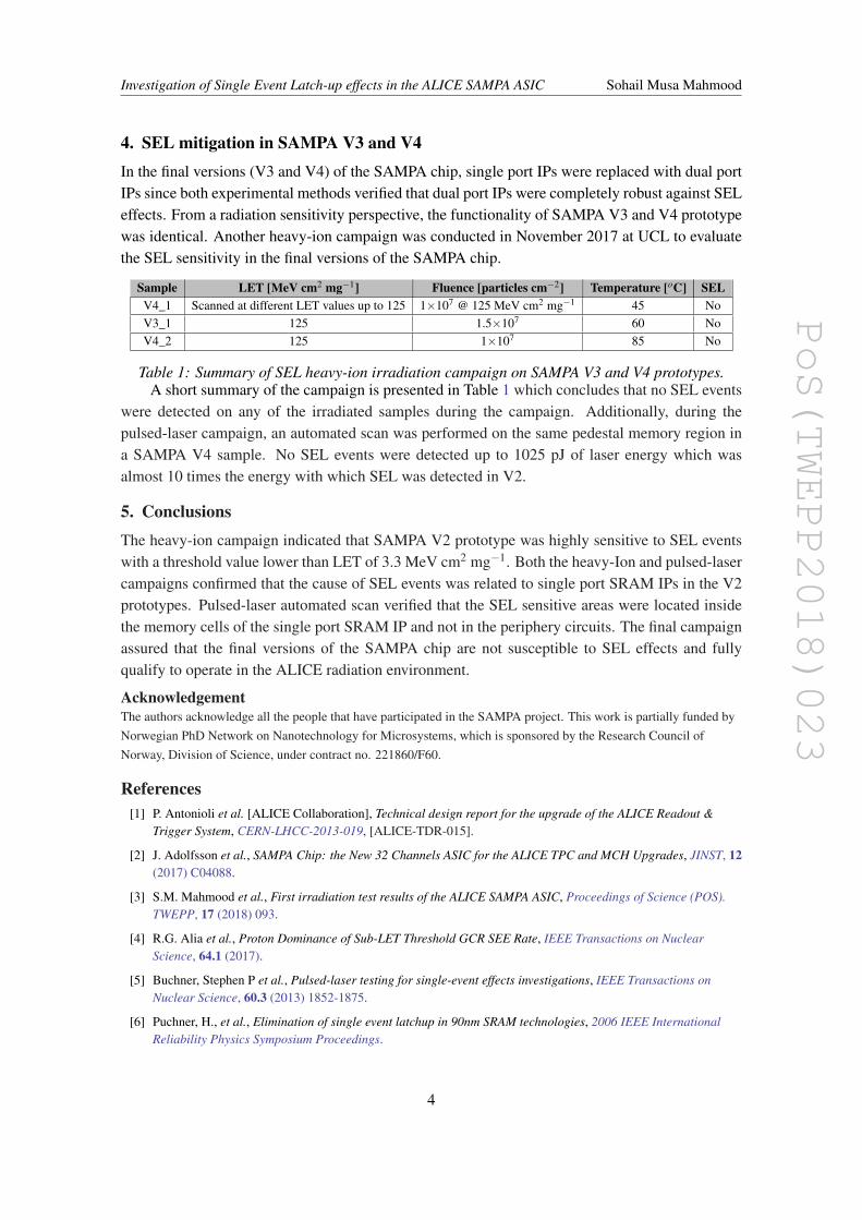
4. SEL mitigation in SAMPA V3 and V4In the final versions (V3 and V4) of the SAMPA chip, single port IPs were replaced with dual portIPs since both experimental methods verified that dual port IPs were completely robust against SELeffects. From a radiation sensitivity perspective, the functionality of SAMPA V3 and V4 prototypewas identical. Another heavy-ion campaign was conducted in November 2017 at UCL to evaluatethe SEL sensitivity in the final versions of the SAMPA chip.
Sample LET [MeV cm2 mg−1] Fluence [particles cm−2] Temperature [oC] SELV4_1 Scanned at different LET values up to 125 1×10⁷ @ 125 MeV cm2 mg−1 45 NoV3_1 125 1.5×10⁷ 60 NoV4_2 125 1×10⁷ 85 No
Table 1: Summary of SEL heavy-ion irradiation campaign on SAMPA V3 and V4 prototypes.A short summary of the campaign is presented in Table 1 which concludes that no SEL events
were detected on any of the irradiated samples during the campaign. Additionally, during thepulsed-laser campaign, an automated scan was performed on the same pedestal memory region ina SAMPA V4 sample. No SEL events were detected up to 1025 pJ of laser energy which wasalmost 10 times the energy with which SEL was detected in V2.
5. ConclusionsThe heavy-ion campaign indicated that SAMPA V2 prototype was highly sensitive to SEL eventswith a threshold value lower than LET of 3.3 MeV cm2 mg−1. Both the heavy-Ion and pulsed-lasercampaigns confirmed that the cause of SEL events was related to single port SRAM IPs in the V2prototypes. Pulsed-laser automated scan verified that the SEL sensitive areas were located insidethe memory cells of the single port SRAM IP and not in the periphery circuits. The final campaignassured that the final versions of the SAMPA chip are not susceptible to SEL effects and fullyqualify to operate in the ALICE radiation environment.
AcknowledgementThe authors acknowledge all the people that have participated in the SAMPA project. This work is partially funded byNorwegian PhD Network on Nanotechnology for Microsystems, which is sponsored by the Research Council ofNorway, Division of Science, under contract no. 221860/F60.
References[1] P. Antonioli et al. [ALICE Collaboration], Technical design report for the upgrade of the ALICE Readout &
Trigger System, CERN-LHCC-2013-019, [ALICE-TDR-015].
[2] J. Adolfsson et al., SAMPA Chip: the New 32 Channels ASIC for the ALICE TPC and MCH Upgrades, JINST, 12(2017) C04088.
[3] S.M. Mahmood et al., First irradiation test results of the ALICE SAMPA ASIC, Proceedings of Science (POS).TWEPP, 17 (2018) 093.
[4] R.G. Alia et al., Proton Dominance of Sub-LET Threshold GCR SEE Rate, IEEE Transactions on NuclearScience, 64.1 (2017).
[5] Buchner, Stephen P et al., Pulsed-laser testing for single-event effects investigations, IEEE Transactions onNuclear Science, 60.3 (2013) 1852-1875.
[6] Puchner, H., et al., Elimination of single event latchup in 90nm SRAM technologies, 2006 IEEE InternationalReliability Physics Symposium Proceedings.
4