Embed Size (px)
Citation preview

POLITECNICO DI TORINO
Collegio di Ingegneria Chimica e dei Materiali
Master of Science Course
in Materials Engineering
Master of Science Thesis
“Optimization of process parameters for
Directed Energy Deposition of IN718 nickel-
based superalloy.”
Thesis Supervisor
Prof. Sara Biamino
Thesis Advisors
Dr. Abdollah Saboori
Dr. Giulio Marchese
October 2019
Candidate
Stefano Di Falco

2

3
Contents 1. Introduction………………………………………………………………………………….1
2. Metal Additive Manufacturing………………………………………………………………3
2.1 Introduction………………………………………………………………………...3
2.2 Brief AM “Pre-History” and “History” …………………………………………...4
2.3 Additive Manufacturing Technologies and Standards……………………………10
2.4 Additive Manufacturing Advantages and Disadvantages………………………...10
2.5 The Additive Manufacturing “Approach” ……………………………………….12
2.6 Metal AM Categories…………………………………………………………….14
2.6.1 Powder Bed Fusion (PBF)……………………………………………...15
2.6.1.1 Selective Laser Melting (SLM)……………………………….16
2.6.1.2 Electron Beam Melting (EBM)……………………………….17
2.6.2 Direct Energy Deposition (DED)……………………………………….19
2.6.2.1 DED Wire feeding……………………………………………20
2.6.2.2 DED Powder feeding…………………………………………22
2.6.2.2.1 Process parameters in LBMD………………………23
2.6.2.2.2 Parameters correlation………………………………26
2.6.3 DED and PBF comparison……………………………………………...29
2.7 Metal AM Applications………………………………………………………….30
2.7.1 DED Aerospace/Aviation applications…………………………………31
2.7.2 Design philosophies and repairing……………………………………...33
2.7.3 Hybrid Additive-Subtractive Manufacturing systems for repairing
operations……………………………………………………………………………………..35
2.8 Ni Superalloys and AM………………………………………………………….38
2.8.1 Microstructure description and Phases…………………………………39
2.8.2 Strengthening by Solid Solution………………………………………..41
2.8.3 Hardening by Precipitation……………………………………………..41
2.8.4 Alloying elements………………………………………………………43
3. IN718 and DED……………………………………………………………………………45
3.1 Melt Pool…………………………………………………………………………45
3.1.1 Chemical-Physical aspects……………………………………………...45
3.1.2 Dynamic Melt Pool and grains morphology……………………………46
3.1.3 Melt-pool cross-section morphology…………………………………...47
3.2 Single Wall…………………………………………………………………………48

4
3.2.1 Grains morphology………………………………………………….….48
3.2.2 Microstructure and phases……………………………………………...50
3.3 SEM / EBSD Analysis in “as-deposited conditions.”……………………………..52
3.3.1 SEM / EBSD: Morphology & Texture in “as-deposited conditions”……52
3.3.2 SEM / EBSD: Phases and chemical composition in “as-deposited”……56
4. Materials and Methods……………………………………………………………………..61
4.1 Feedstock particles………………………………………………………………..61
4.2 DED Machine…………………………………………………………………….62
4.3 Stereomicroscope…………………………………………………………………63
4.4 Cutting…………………………………………………………………………….64
4.4.1 Sampling……………………………………………………………………65
4.5 Mounting………………………………………………………………………….67
4.6 Polishing…………………………………………………………………………..68
4.7 Chemical etching………………………………………………………………….69
4.8 Optical Microscope……………………………………………………………….70
4.9 SEM………………………………………………………………………………70
5. Results and Discussion…………………………………………………………………….71
5.1 Purposes…………………………………………………………………………..71
5.1.1 Features specifications and themes of analysis…………………………... 71
5.2 Single Scan Tracks characterization……………………………………………...72
5.2.1 Single Scan Tracks morphology…………………………………………..73
5.2.2 SSTs and Heat Affected Zone (HAZ) regularity………………………….76
5.2.3 SSTs etched Melt Pools HAZ……………………………………………..80
5.2.4 SSTs etched Melt Pools Morphology……………………………………..80
5.2.5 SSTs etched Melt Pools coherence with the substrate……………………81
5.2.5.1 Melt Pool’s Width, Fusion depth and Bead height……………..82
5.2.6 SST n⁰ 37 - etched Melt Pool’s SEM/EDS
analysis………………………88
5.3 Layers characterization…………………………………………………………...90
5.3.1 Substrate 2 – Inclusions…………………………………………………...90
5.3.1.1 Inclusions Percentage area……………………………………...93
5.3.1.2 Inclusions Average size………………………………………...94
5.3.1.4 Inclusions discussion……………………………………………95
5.3.2 Substrates 1 and 2 – etched layers morphology…………………………...98
5.4 Bulks/Cubes Characterization…………………………………………………...102

5
5.4.1 Defects analysis of the Cubes……………………………………………102
5.4.2 Optical analysis of the etched Cubes…………………………………….104
5.4.2.1 Top of the Cubes………………………………………………106
5.4.2.2 Core of the Cubes……………………………………………...108
5.4.2.3 Bottom of the Cubes…………………………………………..110
5.5 SEM/EDS Cubes’ analysis………………………………………………………112
5.5.1 Laves phases EDS analysis………………………………………………116
5.5.2 δ-phases – EDS analysis…………………………………………………117
5.5.3 Carbides – EDS analysis…………………………………………………117
5.5.4 Oxide layer – EDS analysis……………………………………………...120
5.6 SEM/EDS Substrate……………………………………………………………...122
5.6.1 Carbides………………………………………………………………….122
5.6.2 Laves-phases……………………………………………………………..123
5.6.3 δ-phases…………………………………………………………………..124
6.Conclusions………………………………………………………………………………..127
6.1 SSTs………………………………………………………………………………127
6.2 Layers……………………………………………………………………………..128
6.3 Bulks……………………………………………………………………………...128
7.References…………………………………………………………………………………130
8.Thanks……………………………………………………………………………………..134

Sommario italiano
1. Introduzione
Definita da "McKensey & Company" come uno dei co-protagonisti della "Ops 4.0 Revolution",
l’“Additive Manufacturing” (AM), allo stesso modo della scienza dei Big Data, dell'analisi
avanzata, della robotica e dell'intelligenza artificiale, si propone di essere uno dei settori leader
che, nel prossimo futuro, aumenteranno la produttività industriale del 20% (McKinsey &
Company, 2018). Grazie alle sue caratteristiche di flessibilità, versatilità e ai suoi numerosi
vantaggi, questa recente tecnologia, ha già infatti trovato terreno fertile nei campi più
tecnologicamente avanzati, come quello dell’Aviazione e dell’Automotive, in cui il suo impatto
è stato definito da tecnici ed esperti come "Disruptive"! In particolar modo, l’AM ha attirato un
notevole interesse da parte delle divisioni di ricerca e sviluppo di società leader di molteplici
settori industriali dell’Hi-tech, come l’Aviazione, l’Aerospazio, l’Automotive e il Biomedicale,
grazie alle sue capacità di: produrre componenti dotati di alte performances, ridurre il time to
market, ridurre il peso delle parti, semplificare la supply chain, fornire alta versatilità di
progetto, garantire una produzione On-demand di componenti personalizzati e decentralizzare
la produzione . In particolar modo, fra tutte le famiglie di AM presenti ad oggi sul mercato, la
Metal AM è spesso considerata di primo rilievo quando a richiedersi sono componenti con
performances e proprietà meccaniche superiori, altresì dotati di ottime proprietà di conducibilità
termica ed elettrica. Più nello specifico la Metal AM può essere distinta in due categorie
principali: la Powder Bed Fusion (PBF) e la Directed Energy Deposition (DED). La prima
sfrutta una sorgente laser focalizzata su un letto di polvere al fine di fondere selettivamente le
particelle di feedstock subito prima compattate in un sottile strato (layer) da un rullo/recoater
sulla piattaforma di costruzione. Con la progressiva ritrazione verso il basso di quest’ultima, il
processo viene iterato strato per strato realizzando così una parte 3D. Diversamente, la
tecnologia a deposizione diretta impiega un equipaggiamento composto da un braccio robotico
principale che movimenta spazialmente una testa di deposizione comprensiva nel suo corpo di
un sistema di alimentazione e una sorgente laser passante con asse coincidente a quello della
testa. Nel caso specifico di un’alimentazione a polvere, il materiale particolato fluisce
all’interno degli appositi canali di approvvigionamento sospinto da un gas vettore, che ne
convoglia il particolato in direzione del raggio laser. Spesso inoltre la zona di fusione è
schermata da un gas protettivo (N2 o Ar). Dunque, il processo di deposizione avviene per
fusione locale del substrato (su cui la sorgente energetica è focalizzata) per formazione di una
piscina di fusione “Melt Pool”, dentro la quale vengono intrappolate le particelle del materiale
d’apporto. Tale processo avviene inoltre in modo dinamico, in conseguenza dello spostamento
della testa di deposizione a date velocità trasversale e direzione. La solidificazione del sistema
fisico così composto, corrisponde allora a uno spessore di materiale adeso al substrato di
partenza quasi a significare un cordone di saldatura. Iterando il processo di deposizione è quindi
possibile fabbricare o riparare componenti in tre dimensioni.
Sebbene entrambe le tecnologie perseguano la stessa finalità di ottenimento di parti funzionali
e performanti, fra le due, si evidenziano sostanziali differenze in termini di volumi producibili,
rate di produzione, precisione dimensionale e tolleranze perseguibili, proprietà meccaniche e
finitura superficiale ottenibili. In particolar modo, la tecnologia PBF consente l’ottenimento di
parti funzionali, nel rispetto di ottime tolleranze geometriche e dimensionali (± 005-0,1 mm),
ridotta rugosità superficiale (4-11 µm), e con microstrutture generalmente molto fini che si
traducono in proprietà meccaniche elevate. Differentemente, rispetto alla tecnologia PBF, la
deposizione diretta DED fornisce accuratezza geometrica delle parti inferiore (di ± 25 mm) e

ii
una rugosità superficiale maggiore (di circa 25 µm). Inoltre, la microstruttura derivante dal
processo a deposizione diretta, se paragonata a quella ottenibile via LPBF, risulta essere più
grossolana e marcatamente anisotropa. Tuttavia, i maggiori vantaggi forniti dalla tecnologia
DED sono da riconoscersi nella capacità di produrre componenti massivi aventi volumi non
egualmente ottenibili con altre tecnologie AM, poiché limitate dagli ingombri delle camere di
stampa. Non di meno, l’alto grado di mobilità spaziale del braccio robotico, insieme alla
possibilità di movimentare il piatto di stampa nelle tre dimensioni, fornisce fino a 9 gradi di
libertà che consentono quindi un enorme flessibilità produttiva. In ragione di tale confronto,
appare dunque evidente che la scelta di una famiglia rispetto all’altra sia dettata, più che da
valori di merito, dalle esigenze dei differenti casi applicativi.
Tuttavia, uno dei limiti più costrittivi che accomuna ambedue, sono i costi di produzione quando
volumi medio-grandi di componenti sono richiesti. Infatti, il vantaggio economico nel produrre
componenti via AM, surrogando i processi produttivi convenzionali, è tutt’oggi fortemente
limitato a settori industriali di nicchia e alla produzione di tirature limitate dove si richiede un
elevata complessità delle parti. Piuttosto, in molti casi si ricerca la coesistenza della produzione
additiva con i processi di manufacturing tradizionali al fine di sfruttare i vantaggi di
complementarietà di entrambe le tecnologie.
Un esempio di coerenza fra processi produttivi convenzionali e Metal AM, è rappresentato dalla
possibilità di utilizzare sistemi ibridi DED-CNC (Figura 1), per riparare stampi o componenti
funzionali danneggiati e precedentemente costruiti tramite processi convenzionali. Con tali
apparati, è infatti possibile depositare nuovo materiale in corrispondenza delle aree difettate,
rifinendo poi forma tolleranze e superfici tramite operazioni sottrattive, riducendo così a
obsoleta la necessità di fabbricare ex novo altri componenti. In modo particolare, quest’ultimo
caso applicativo è preso in analisi nel presente incarico di tesi.
Figura 1: Apparato ibrido DED-CNC di fabbricazione additiva e sottrattiva (Villeneuve et al., 2018)
Inoltre, la possibilità di questi apparati di riparare i componenti danneggiati non richiedendo
complesse attrezzature e in modo versatile, per esecuzione di processo e impiego di materiali,
risponde perfettamente alle esigenze manifestate dall’Aviazione. Infatti, la gran parte dei

iii
componenti avionici è progettata secondo una filosofia di design “Damage tolerance” che
prevede di tracciare lo stato di vita del componente, in relazione allo stato di avanzamento delle
cricche o dei danneggiamenti all’interno di esso, stabilendo aprioristicamente un punto di
ispezione e ripristino dello stesso (Figura 2). Proprio in questa istanza un apparato ibrido DED-
CNC risulterebbe adatto a compiere operazioni di riparazione estendendo la vita del
componente.
Figura 2: Diagramma resistenza-tempo di vita di un componente avionico progettato “Damage tolerant” e riparato
(Alderliesten, 2018).
Riconducendosi almeno in prima approssimazione allo scenario appena esposto, nel presente
incarico di tesi si riportano i risultati di una campagna sperimentale volta a identificare i
parametri di processo ottimali con cui settare un apparato DED alimentato a polveri di IN718.
Ipotizzando che tale apparato possa essere integrato in uno ibrido DED-Laser ablation-milling,
tali parametri di processo potrebbero essere dunque impiegati per compiere deposizioni additive
e riparative di componenti avionici danneggiati in IN718.
A tale fine, tre differenti tipologie di “caratteristiche” in IN718 costruite a differenti valori di
potenza laser P e velocità di deposizione F su un substrato di IN718 non preriscaldato, sono
state analizzate sotto molteplici aspetti.
Più nel dettaglio le caratteristiche prese in analisi sono:
40 Singole tracce uniche fra loro (Single Scan Tracks-SSTs)
20 Singoli Layers unici fra loro (SLs) suddivisi nei due differenti substrati 1 e 2
3 Cubi depositati impiegando i medesimi parametri di processo (Cubes)
1.1 Ulteriori specifiche e temi di analisi:
- Le SSTs sono state realizzate impiegando:
8 livelli di Feed rate, F [mm/min]: 300, 450, 600, 750, 900, 1050, 1200, 1350
5 livelli di Laser Power, P [W]: 300, 400, 500, 600, 700.
e caratterizzate nella loro:
morfologia
regolarità della loro zona termicamente alterata (ZTA)
morfologia e regolarità dei “Melt Pools” osservati lungo le cross-sections delle
SSTs dopo attacco chimico.
coerenza con il substrato

iv
- I SLs del “Substarto 1” sono stati realizzati impiegando:
un’unica Potenza laser, P [W]: 600
2 velocità di deposizione, F [mm/min]: 750, 900
2 Hatching distances, Hd [mm]: 0,3, 0,4
mentre quelli del “Substrato 2” utilizzando:
un’unica Potenza laser, P [W]: 400
2 velocità di deposizione, F [mm/min]: 750, 900
2 Hatching distances, Hd [mm]: 0,3, 0,4.
Inoltre, I SLs di ogni substrato sono stati caratterizzati in:
area percentuale di defettologie
morfologia delle deposizioni dopo attacco chimico
- I Cubi sono stati realizzati impiegando:
un’unica Potenza laser, P [W]: 750
un’unica velocità di deposizione, F [mm/min]: 900
un’unica Hatching distance H [mm]: 0,3
layer thickness dz [mm]: 0,2
la strategia di hatching “Raster”: 0⁰ /90⁰ /45⁰ /135⁰ /60⁰ /120⁰
e caratterizzati in:
area percentuale di defettologie
morfologia della microstruttura
area percentuale delle fasi laviche
tipologia delle fasi presenti
dimensioni e composizione dello strato di ossido sopra formatosi.
2. Materiali e Metodi
2.1 Polveri
Il feed-stock che è stato utilizzato per alimentare l’apparato DED è costituito da polveri sferiche
di IN718, ottenute tramite processo di atomizzazione a gas, aventi taglia media grossolana
compresa fra 44 e 106 µm. L’analisi morfologica superficiale condotta tramite microscopia
ottica a scansione, ha inoltre permesso di rivelare la non uniformità di forma delle particelle
evidenziando la presenza di particelle satellitari adese alla superficie di quelle principali.
L’analisi EDS di composizione di superficie, ha invece rivelato la presenza di Ni, Cr, Fe,O e
Nb oltre a una modesta percentuale di Ti e Al (Figura 3), elementi potenziali formatori di
composti e ossidi non desiderati.

v
Figura 3: Analisi EDS composizionale della superficie delle polveri
Volendo approfondire l’aspetto composizionale, l’analisi EDS è stata applicata anche alle
cross-sections delle particelle evidenziando la presenza non trascurabile di porosità interne e di
ossidi di alluminio (Figura 4). La genesi di queste defettologie è stata imputata alla scelta di
eseguire il processo di atomizzazione in un’ atmosfera non inerte.
Figura 4: Analisi SEM delle cross-sections delle polveri di feedstock.
2.2 Stereomicroscopio
Le caratteristiche in oggetto di analisi in questa campagna sono state dapprima analizzate nella
loro morfologia superficiale tramite un’analisi ottica allo stereomicroscopio LEICA EZ4W.
Tale metodologia di ispezione ha permesso dunque di determinare le regolarità o irregolarità di
forma delle caratteristiche e quindi valutare macroscopicamente la conformità di deposizione
delle stesse.
2.3 Taglio dei campioni e inglobamento
I substrati contenenti le caratteristiche da essere analizzate sono stati tagliati tramite la Cutting
Machine “Remet TR 100s”, equipaggiata con una lama CERMET al carburo di silicio,
campionando dunque le stesse nei volumi minimi di materiale che le potessero contenere.

vi
Ulteriormente, ogni campione, è stato sezionato lungo il piano di sezione trasversale delle
caratteristiche. I campionamenti così ottenuti, sono stati successivamente inglobati in una
matrice polimerica termoindurente a costituire una montatura adatta alla corretta e agile
manipolazione del campione nelle successive operazioni di lucidatura.
2.4 Lucidatura e attacco chimico
La lucidatura delle caratteristiche, operazione indispensabile da eseguirsi per permettere
l’osservazione microscopica, è stata eseguita tramite una polishing machine “Presi Mecatech
234” utilizzando un set di carte abrasive rispettivamente indicizzate: #FEPA 320, 600, 800,
1200, 2400 e 4000. Infine, è stata eseguita una lucidatura più spinta atta a portare la rugosità
media superficiale prima a 3 e poi 1 µm tramite l’ausilio di due panni in feltro cosparsi di una
soluzione di lubrificante e pasta diamantata. A titolo di esempio, si riportano le immagini delle
superfici così lucidate delle SSTs, ossevate a microscopio ottico in Figura 5.
Figura 5: Sezioni trasversali delle SSTs dopo lucidatura osservate a 50X per microscopia ottica.
Dopo la loro lucidatura, i campioni sono stati attaccati chimicamente con la soluzione Kalling’s
n⁰ 2 di composizione:
- CuCl2 10 gr
- Hydrocloridic acid 200 ml
- Ethanol absolute 200 ml
I provini sono stati pertanto immersi nella soluzione per un tempo medio di 15s prima di essere
spenti in acqua distillata. Tale trattamento di incisione chimica metallografica, ha permesso ai
processi corrosivi di prendere luogo con rates di corrosione differenti a seconda che
interessassero fasi e microstrutture diverse. La superficie così preparata e la sua microstruttura
sono state successivamente osservate tramite il microscopio ottico LEICA DMI 5000 agli
ingrandimenti 50X e 100X.

vii
2.6 Microscopia a scansione SEM ed analisi EDS
L’osservazione delle fasi microstrutturali e l’analisi di composizione sono state eseguite tramite
un microscopio SEM da banco “Phenom XL”, equipaggiato con rivelatore di RX per l’analisi
EDS. Al fine di rendere possibile l’analisi mediante irraggiamento elettronico i campioni
metallici sono stati liberati dalla loro montatura plastica permettendo dunque la piena
funzionalità delle loro proprietà di conduzione elettrica.
3. Risultati sperimentali
Al fine di individuare la migliore combinazione di potenza laser e di velocità di deposizione, la
conformità delle singole 40 coppie di valori di F e P è stata valutata analizzando le deposizioni
rispettivamente ottenute. Tramite un primo processo ad esclusione, si sono considerati come
conformi i parametri di processo che fornissero deposizioni regolari, omogenee, la cui ZTA
avesse valori contenuti, e che esibissero Melt Pools simmetrici e con dimensioni caratteristiche
funzionali a garantire un corretto processo di sovrapposizione degli stessi. In base all’analisi
delle cross-sections dei SLs, è stato scelto invece il valore di Hd ottimale, riscontrato in
corrispondenza dei layers più densi e aventi migliore regolarità superficiale. I risultati ottenuti
hanno dunque indicato i parametri di processo P 600W, F 750 mm/min e Hd 0.3 mm, come
ottimali per eseguire operazioni di riparazione funzionali nel rispetto del miglior compromesso
fra minimizzazione dei tempi di processo e risparmio di materiale. In ultimo luogo un’analisi
più approfondita ha riguardato la detezione delle defettologie e l’osservazione delle
caratteristiche microstrutturali nelle cross-sections dei 3 cubi costruiti impiegando i parametri
di ottimizzazione appena riportati.
3.1 Morfologia delle SSTs
Tramite stereo-microscopia è stata condotta un’analisi on-top delle SSTs all’ ingrandimento
10X, ottenendo una prima mappa di ottimizzazione nella quale distinguere le zone di processo
non conformi da quelle conformi (Figura 6).
Dunque, la conformità morfologica delle SSTs è stata valutata secondo i due parametri di
giudizio principali di:
Omogeneità delle deposizioni
Regolarità del profilo
Pertanto, dall’analisi dei risultati raccolti:
a) si evidenziano due instabilità di processo in corrispondenza delle deposizioni 21 e
25 (contornate in blu) ottenute rispettivamente tramite le due coppie di parametri P
500W, F 900 mm/min e P 400W, F 3000 mm/min.
b) si riconosce una finestra di non conformità in corrispondenza di valori medio bassi
di velocità di scansione e alti valori di potenza laser impiegata. La stessa è stata
contornata in colore rosso.
Le cause delle suddette defettologie sono state rispettivamente riconosciute in:
viii
a) – una probabile improvvisa accelerazione della testa di deposizione e/o in un non
corretto approvvigionamento di polveri della zona di fusione da parte dei feeders.
– una scarsa potenza laser non sufficiente a fondere le particelle di polvere flussate
nell’unità di tempo resa disponibile dalla velocità di scansione.
b) una troppo alta energia specifica che ha comportato un’interazione troppo severa
con il substrato, dunque causando una alta ZTA e disomogeneità di deposizione in
conseguenza di una troppo alta bagnabilità del materiale fuso.
Figura 6: SSTs all’ ingrandimento 10X: conformi se contornate in verde (omogeneità di deposizione) non
conformi se contornate in rosso (disomogeneità di deposizione).
ix
3.2 ZTA delle SSTs
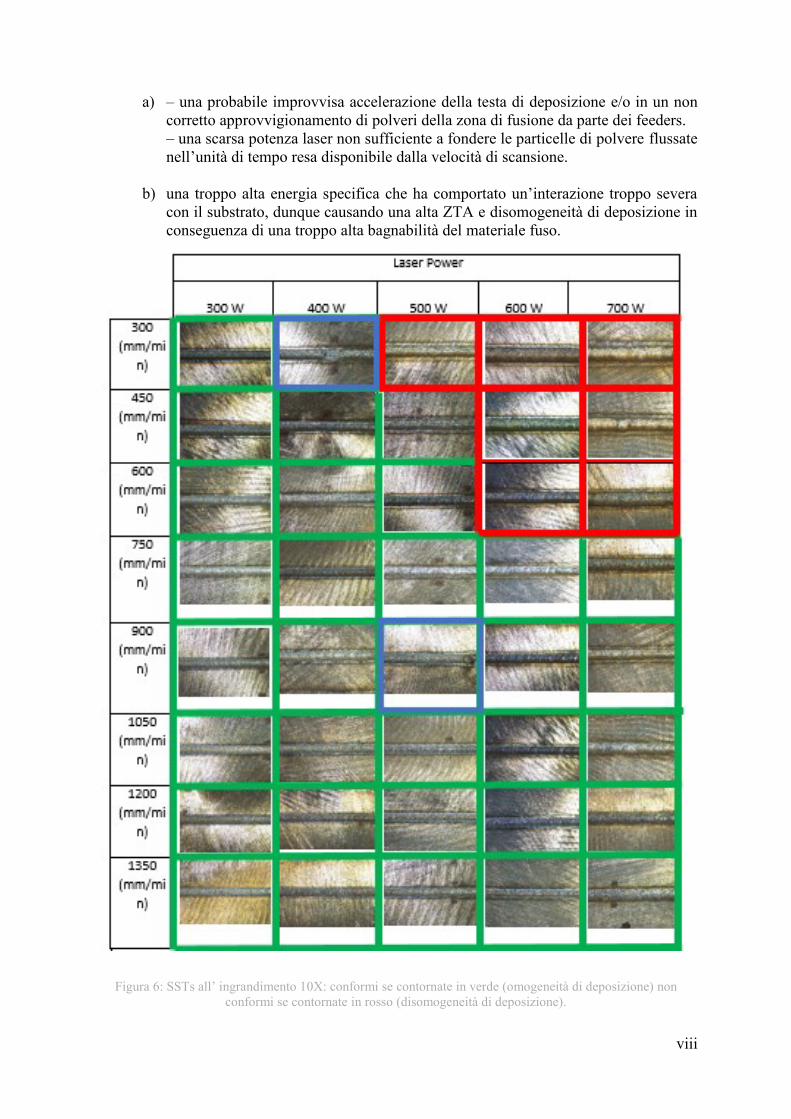
Volendo inoltre valutare l’omogeneità e la regolarità dell’interazione laser con il substrato, la
zona termicamente alterata è stata misurata nella sua larghezza e quindi nella sua deviazione
standard lungo il profilo delle tracce.
Più precisamente, non è stato possibile riferirsi a precisi valori soglia della ZTA su cui basare
un’analisi di conformità ad esclusione.
Tuttavia, è stato possibile osservare che:
- la larghezza della zona termicamente alterata diminuisce con l’incremento della velocità
di scansione a parità di potenza laser impiegata.
- la larghezza della zona termicamente alterata aumenta con l’incremento della potenza laser a parità di velocità di scansione.
- le SSTs
I risultati ottenuti sono stati dunque riportati:
- in Figura 7 ove indicati i valori della larghezza media della ZTA e delle relative
deviazioni standard
Figura 7: Media aritmetica "A" e Deviazione Standard "SD" della larghezza della ZTA in funzione della potenza
laser P e della velocità di deposizione F
3.3 Analisi microscopica ottica dei “Melt Pools” attaccati chimicamente
L’analisi microscopica ottica delle cross-sections ha permesso di analizzare i pozzetti di fusione
considerando come parametro chiave per ottenere una corretta sovrapposizione laterale e
HAZ

x
trasversale delle tracce, la loro simmetria. Ulteriormente, sono state valutate le dimensioni
principali dei “Melt Pools” al fine di valutare il grado di penetrazione e coerenza delle
deposizioni con il substrato, oltre all’eventuale presenza di defettologie come il “Key holes”
(difetto dovuto a interazioni troppo severe della sorgente laser con il substrato).
I parametri chiave di giudizio utilizzati in questo campo di analisi sono stati dunque:
- la simmetria dei pozzetti di fusione
- la valutazione delle dimensioni caratteristiche “Width”, “Bead Height” e “Fusion
Depth” (Figura 8).
Figura 8: SST "37" e le sue dimensioni principali: Melt Pool Width, Bead Height, Fusion Depth e HAZ
I risultati dell’analisi geometrica di simmetria hanno dunque evidenziato (Figura 9):
- la non conformità di utilizzo della potenza laser 400W in corrispondenza della quale i
Melt Pools delle SSTs 26, 27, 28, 29, 30, 31 e 32 mostrano evidenti asimmetrie
geometriche.
- la parziale non conformità di utilizzo della potenza laser 300 W in corrispondenza della
quale i Melt Pools delle SSTs 10, 11, 12, 13 mostrano asimmetrie geometriche.
- un'unica defettologia è stata riscontrata a 500W nel Melt Pool della SST 22.
La misura invece delle dimensioni caratteristiche ha evidenziato gli andamenti generali (Figure
10,11,12,13):
- la Bead height diminuisce a parità di P se il feed rate cresce
- la Width e la Fusion Depth aumentano se P aumenta a parità di F
- tutte e tre le caratteristiche diminuiscono all’aumento della velocità di scansione
- un insufficiente decrescita del rapporto “Width” / “Fusion Depth” a causa di un troppo
modesto valore di feed rate, che ha comportato melt pools aciculari e non
geometricamente bilanciati
- un insufficiente decrescita del rapporto “Width/Bead Height” a causa di un troppo
modesto valore di feed rate, che ha comportato melt pools con bassi bead height e non
geometricamente bilanciati.

xi
Tuttavia, sebbene gli andamenti sopra citati risultano essere generalmente validi, diverse
eccezioni sono state rilevate:
- le SSTs 8, 23, 33 e 37 mostrano una Width inferiore di quella attesa rispetto ai parametri
impiegati
- le SSTs 1 e 21 mostrano una Fusion Depth inferiore di quella attesa.
- le SSTs 22, 23 e 28 mostrano valori sottostimati del loro rapporto Bead Height/Width a
causa dell’alta velocità trasversale che fa decrescere il valore di Powder Density.
Figura 9: cross-sections dei“Melt Pools” attaccati chimicamente – Analisi ottica a 50X

xii
Figura 10: SSTs – Melt Pools’ Width in funzione della potenza laser
Figura 11: SSTs- Fusion Depth e Bead Height in funzione della potenza laser
Fusion
Depth
Bead
Height
t

xiii
Figura 12: SSTs – rapporto fra Melt Pool width e Fusion Depth in funzione della potenza laser
Figura 13: SSTs – rapporto fra Melt Pool width e Fusion Depth in funzione della potenza laser
Al fine di riassumere tutti i risultati di analisi ottenuti, si presenta in Tabella 1 una raccolta delle
conformità e non conformità delle SSTs relativamente ai parametri di processo con cui le stesse
sono state ottenute.

xiv
Tabella 1: Raccolta delle conformità e non conformità delle SSTs
Cross sectional
analysis
Las
er P
ow
er (
W)
Fee
d R
ate
(mm
/min
)
SS
T n
um
ber
Pro
cess
sta
bil
ity
SS
T r
egu
lari
ty
Mel
t P
oo
l
sym
met
ry
Melt Pool
coherence
with the
substrate
Wid
th
F.
Dep
th
B.
Hei
gh
t
600
300 1
450 2
600 3
750 4
900 5
1050 6
1200 7
1350 8
300
300 9
450 10
600 11
750 12
900 13
1050 14
1200 15
1350 16
500
300 17
450 18
600 19
750 20
900 21
1050 22
1200 23
1350 24
400
300 25
450 26
600 27
750 28
900 29
1050 30
1200 31
1350 32
700
300 33
450 34
600 35
750 36
900 37
1050 38
1200 39
1350 40

xv
In ultima istanza si evince dunque che:
- la potenza laser di 700W comporta un’interazione troppo severa con il substrato (quindi
estesa ZTA ed inomogeneità di deposizione), dovuta a valori di energia specifica troppo
alti e non opportunamente bilanciati con le velocità di deposizione considerate.
- la potenza laser di 400W produce deposizioni asimmetriche con pronunciata e irregolare
ZTA.
- la migliore soluzione in termini di minimizzazione delle defettologie è rappresentata
dalla scelta di velocità di scansione medio-alte che compensino l’energia specifica
fornita e quindi minimizzino le inomogeneità e le irregolarità deposizionali.
- la migliore soluzione in termini di massimizzazione delle dimensioni caratteristiche è
rappresentata dalla scelta di velocità di scansione basse, unitamente all’aumento del
valore di feed rate (quantità di polvere flussata in unità di tempo).
Pertanto, si è riconosciuto per valori intermedi di velocità di deposizione e potenza laser, il
miglior compromesso fra massimizzazione delle dimensioni dei Melt Pools e minimizzazione
delle defettologie.
In ragione di quanto detto sono stati preselezionati come ottimali le coppie di valori
- P: 400W e 600W
- F: 750 mm/min e 900 mm/min
3.4 Analisi microscopica ottica dei “Layers” – Detezione delle defettologie
Le due coppie di valori identificati come ottimali dall’analisi delle SSTs, sono state impiegate
per realizzare:
- 12 Layers impiegando P 600W e F 750/900 mm/min (Substrato 1) * - * 4 di questi non sono stati analizzati poiché difettati
- 12 Layer impiegando P 400W e F 750/950 mm/min (Substrato 2)
L’analisi per microscopia ottica delle sezioni trasversali (non attaccate chimicamente) del
Substrato 2 ha rivelato:
- il valore massimo di area percentuale delle defettologie dello 0.06%, in corrispondenza
dei layers ottenuti impiegando F 750 mm/min.
- la dimensione media massima delle defettologie di 41,7 µm, in corrispondenza dei
layers ottenuti impiegando F 900 mm/min.
- defettologie di forma prevalentemente circolare, in prima assunzione riferibili a una
presenza promiscua di porosità e ossidi.
Le possibili cause che possono aver portato alla genesi di tali defettologie, sono state imputate:
- alla non adozione di “Shielding gas”, la quale ha permesso all’ossigeno presente in
atmosfera di formare ossidi
- all’intrappolamento di “Carrier gas” nel metallo fuso che ha così formato pori circolari
- alla presenza di porosità e ossidi nel feedstock di partenza che, una volta fuso, ha
trasferito le sue defettologie alla parte.

xvi
Tuttavia, potendo considerare la presenza percentuale di difetti come modesta, gli stessi non
sono stati considerati come uno dei parametri chiave su cui basare l’analisi di conformità delle
deposizioni. Per questa ragione, la medesima analisi non è stata intrapresa anche per il Substrato
1.
3.5 Analisi microscopica ottica dei “Layers” – Analisi di coerenza delle deposizioni con il
substrato.
La coerenza dei layers con il substrato è stata valutata osservando le cross-sections dei layers
(attaccate chimicamente) nella loro morfologia. In particolare, sono stati valutati il grado di
sovrapposizione laterale delle tracce e l’omogeneità di deposizione, in relazione ai valori di P
ed F impiegati e in base alle due “Hatching distance” adottate di 0,3 mm e 0,4 mm.
Al fine di selezionare la migliore combinazione di parametri, la migliore deposizione del
Substrato 1 e del Substrato 2, ottenute rispettivamente a 600W (e 900 mm/min, 0,4 mm) e a
400W (e 750 mm/min, 0,3 mm), sono state confrontate (Figura 9).
Figura 9: a) SLs 9 del Substrato 1 e b) 6 del Substrato 2 (a destra)
I risultati dell’analisi morfologica di confronto hanno pertanto rivelato:
- dimensioni caratteristiche dei melt pools superiori negli strati depositati a 600W
- superiore sovrapposizione laterale delle singole tracce depositate a 600W
- notevole disomogeneità morfologica delle deposizioni ottenute a 400W
In ragione di tali risultati, la potenza laser di 600 W è stata selezionata come ottimale da
impiegarsi per realizzare le caratteristiche in esame nella seguente campagna.
Infine, volendo massimizzare l’omogeneità deposizionale e la stabilità di processo, si sono
scelti come parametri ottimali la velocità di deposizione F 750 mm/min e la distanza di
Hatching di 0,3 mm. Infatti, sebbene tale scelta sia in contro tendenza con la ricerca della
massimizzazione di produttività, si è scelto di porre l’enfasi sull’affidabilità di processo e
minimizzazione delle defettologie vista la natura dell’applicazione e dei componenti da
ripararsi. A parità di potenza laser infatti, più modeste velocità di deposizione comportano
Substrato
Strato depositato
Interfaccia
a) b)

xvii
aumento della Width dei Melt Pools la quale, unitamente a Hd ridotte, permette una più marcata
giunzione laterale delle SSTs senza formazione di pori.
3.6 Analisi microscopica ottica dei “Cubes” – Detezione delle defettologie A conclusione della campagna sperimentale, sono state analizzate le cross-sections di tre cubi depositati con i parametri di ottimizzazione precedentemente selezionati. Similarmente all’analisi delle defettologie intrapresa per gli strati, i cubi sono stati osservati per microscopia ottica potendo così quantificare la loro area percentuale e dimensione media rispettivamente in 0,04% e 14,8 µm. Si è notato inoltre che tali valori si dimostrano essere pur inferiori a quelli trovati nei Layers (del Substrato 2) costruiti con gli stessi parametri di processo, fornendo dunque un ulteriore conferma che la potenza laser di 600W rappresenti la migliore scelta. In aggiunta, nessuna particolare defettologia come Keyholes o Lacks of fusion è stata riscontrata.
3.7 Analisi microscopica ottica dei “Cubes” – Morfologia della microstruttura Tramite microscopia ottica, è stato inoltre possibile osservare la morfologia microstrutturale delle parti agli ingrandimenti 50X e 100X. Più precisamente l’analisi ha preso in esame le tre zone differenti del cubo: “Top”, “Core” e “Bottom”. I risultati dell’analisi hanno pertanto fornito le seguenti osservazioni “Bottom”
- dalla zona inferiore si estende verso il centro della parte una microstruttura dendritica colonnare e fine.
- la zona di interfaccia fra la parte e la base risulta essere omogenea, coerente e con una modesta ZTA (a differenza di quanto rilevato per la SST 4 ottenuta impiegando i medesimi parametri)
Figura 10: Crescita epitassiale e colonnare dendritica dal substrato verso il core della parte – Micrografia
ottica a 50X

xviii
“Core”
- nel centro dei cubi non è stata rilevata presenza di defettologie come Lack of fusions o Key Holes
- una crescita colonnare dendritica attraversa coerentemente gli strati e le singole tracce sovrapposte suggerendo così una crescita epitassiale
- la strategia di deposizione insieme al forte carattere direzionale di solidificazione tipico del processo DED, hanno comportato una forte anisotropia microstrutturale testimoniata anche dall’effetto “stair-case” (Figura 11).
Figura 11: Effetto "stair case" in cui si distingue un netto cambio di direzionalità della microstruttura da un SL
all'altro
“Top”
- nella zona in prossimità della superficie si è osservata una zona di transizione a demarcare la struttura colonnare proveniente dal centro del cubo e una microstruttura cellulare equiassiale situata in prossimità dei bordi. Tale variazione morfologica è in accordo con la diminuzione locale del rapporto G/R (Figura 12).
Figura 12: Micrograph of the etched Cube 6 top acquired at 100X (optical microscope) - transition from
columnar to equiaxed microstructure.

xix
3.8 Analisi microscopica a scansione ed EDS dei “Cubes”
Al fine di ispezionare più approfonditamente la microstruttura è stata eseguita un’analisi di
microscopia a scansione nelle medesime aree analizzate tramite microscopia ottica. Eseguendo
una mappatura dei campioni ai tre ingrandimenti 1000X, 2000X e 3000X, è stato possibile
evidenziare:
- una rilevante presenza percentuale di fasi “Laves” inter-dendritiche seppur non
quantificabile tramite i metodi di analisi utilizzati
- inattesa presenza di fasi “Laves” nelle aree prossime ai bordi delle caratteristiche,
nonostante il basso gradiente termico locale.
Pertanto, la rimarcata anisotropia microstrutturale evidenziata dapprima dalla microscopia
ottica e qui rimarcata dalla microscopia a scansione, indica una forte discontinuità delle
proprietà del materiale. Per tale motivo, le caratteristiche “as-deposited” non possono costituire
una soluzione pronta all’ uso, ma piuttosto, prima della loro messa in opera si deve prevedere
un trattamento termico al fine di dissolvere le fasi laviche e le spesso presenti fasi delta. Inoltre,
al fine di identificare le fasi presenti all’interno delle parti, è stata condotta un’analisi EDS, la
quale ha dimostrato la presenza di:
- Carburi dispersi nella matrice γ
- Ossidi di Ti e Al
- Fasi “Laves”
- Fasi delta
- Ossidi di Ti e Al all’interno dello strato di ossido che ricopre la superficie della parte.
4. Conclusioni
IN questo incarico di tesi è stata presentata una campagna sperimentale che ha interessato la
caratterizzazione di tre caratteristiche: (SSTs, SLs e Cubes), realizzate in superlega a base Ni
IN718 e fabbricate tramite la tecnologia di produzione additiva “Directed Energy Deposition”
(DED) con alimentazione a polvere. Più nel dettaglio, 40 singole tracce sono state analizzate
nel loro aspetto morfologico e nelle loro caratteristiche microstrutturali identificando così una
prima finestra di conformità del processo. Successivamente, la caratterizzazione ha interessato
le due più massive caratteristiche “SLs” e “Cubes”. Dai risultati ottenuti in laboratorio e dalle
analisi eseguite si possono trarre le seguenti conclusioni:
6.1 SSTs
L’analisi on-top delle SSTs ha riportato:
- che tutte le SSTs mostrano regolarità del loro profile eccetto le tracce no. 1, 2, 3, 17,
33, 34, and 35.
- che le SSTs 21 e 25 sono state depositate non conformemente poiché testimoni di
instabilità di processo
- la Potenza laser di 700W causa una troppo severa interazione col substrato
comportando quindi lo sviluppo di una ZTA troppo pronunciata
L’analisi delle sezioni trasversali attaccate chimicamente delle SSTs ha riportato:
- l’assenza di defettologie “Key hole”

xx
- la notevole asimmetria dei pozzetti di fusione delle SSTs:
no. 26,27,28,29,30,31 and 32 (ottenute a 400W)
no. 10,11,12,13 (ottenute a 300W)
no. 22
L’analisi delle dimensioni principali dei melt pools ha evidenziato:
- la progressiva diminuzione della “Fusion depth”, “Width” e “Bead Height” dei melt
pools all’incremento della velocità di scansione a parità di potenza laser impiegata
- la “Width” e la “Fusion Depth” crescono se la potenza laser power P cresce a parità
della velocità di scansione
- la “Bead Height”, quindi la “layer thickness” diminuisce a parità di P se la velocità
di scansione cresce
- un valore di feed rate non conforme per alimentare la testa di deposizione che ha
comportato valori dei rapporti “Fusion Depth/Width” e “Bead Height Width
notevolmente scostati dal valore ideale “1” e quindi indicanti melt pools non bilanciati
nelle loro dimensioni principali.
Tutte le non conformità rilevate delle SSTs sono state riassunte in Tabella 1
In conseguenza dell’analisi delle non conformità si è dunque dedotto che:
-i valori medi di velocità di scansione 750,900 mm/min e I valori medi di potenza
laser,600W sono da considerarsi nel caso applicativo considerato come ottimali
-la miglior soluzione in termini di minimizzazione delle defettologie è perseguibile
tramite l’adozione di valori di velocità di scansione medio alti che ben compensino
l’energia specifica fornita nell’unità di tempo
-la miglior soluzione in termini fi massimizzazione delle dimensioni caratteristiche dei
melt ools è perseguibile tramite l’adozione di basse velocità di scansione e un magggiore
feed rate di quello adottato.
6.2 SLs
L’analisi ottica delle cross-sections dei “SLs” non attaccati chimicamente ha rivelato:
- La presenza di due tipi di defettologie: “ossidi” e “pori”, tuttavia non distinguibili nelle
loro quantità relative tramite le metodologie di analisi usate
- La massima area percentuale dei difetti di 0,06%, rilevata in corrispondenza dei “SLs”
costruiti con F 750 mm/min (Substrato 2)
- La massima taglia media dei difetti di 41,7 µm, rilevata in corrispondenza dei “SLs”
costruiti con F 900 mm/min (Substrato 2)
- Considerando la modesta presenza di defettologie, non si è ritenuto necessario replicare
la stessa analisi per il Substrato 1
L’analisi ottica delle cross-sections attaccate chimicamente ha evidenziato:
- superiorità di caratteristiche microstrutturali e morfologiche dei “SLs” costruiti a 600W
- superiorità di sovrapposizione laterale delle single trace costituenti i “SLs” costruiti a
600W

xxi
- forte inomogeneità delle deposizioni ottenute a 400W
- la Potenza laser di 600W rappresenta il valore di P ottimale da adottarsi nel caso
applicativo considerato
- la “hatching distance” Hd di 0,3 mm e la velocità di scansione F of 750 mm/min come
coppia di parametri adatta a minimizzare le defettologie e massimizzare la produttività.
6.3 Cubes
L’analisi ottica delle “cross-sections” attaccate chimicamente ha rivelato:
“Bottom”
- una crescita dendritica colonnare che si protende a partire dal substrato fino al centro
della parte
- che l’interfaccia compresa fra il substrato e la parte è omogenea e coerente mostrando
una ZTA ridotta
Core
- l’assenza di defettologie tipiche quali “Key hole” e “Lack of fusion”
- che la crescita dendritica attraversa le diverse trace e strati all’interno della parte a
suggerire una crescita epitassiale
- che la strategia di scansione unitamente al forte carattere di solidificazione direzionale
tipico del DED, hanno comportato una forte anisotropia microstrutturale.
Top
- una zona di transizione nelle vicinanze dei bordi delle parti, a ripartire una crescita
cellulare equiassica da una dendritica e colonnare
L’analisi SEM/EDS ha invece riportato:
- una considerevole presenza di fasi “Laves” nelle regioni interdendritiche non
direttamente quantificabili mediante le metodologie di analisi utilizzate
- presenza di fasi di “Laves” in prossimità della superficie nonostante questa in
costruzione fosse interessata da modesti gradienti termici locali
- presenza di carburi ricchi in Nb e Ti dispersi nella matrice γ
- presenza di ossidi di Ti e Al
- fasi “delta”
- ossidi di Ti e Al nello strato di ossido ricoprente la parte; di spessore 72µm e
15µm rispettivamente sulla sommità e sulle pareti.
Per concludere, i parametri di ottimizzazione scelti al fine di massimizzare l’efficienza del
processo DED sono: potenza laser P di 600W, velocità di scansione F di 750 mm/min e
Hatching distance di 0,3 mm.

xxii
Abstract
In this Thesis assignment, the goal was to find the optimum process parameters to produce
Inconel 718 alloy via Directed Energy Deposition (DED). Therefore, for this purpose, the
experimental analysis considered three different steps in which the optimum process parameters
are achieved step by step. More in detail, the characterisation regarded: 40 “Single Scan Tracks”
(SSTs), 24 “Single Layers” (SLs) and 3 “Cubes”. Indeed, the laser-related parameters like laser
power (P), laser scan speed (SS) were selected according to the SSTs analysis, whereas the
optimum hatching distance (Hd) was estimated according to the SLs. The best melt pool in
terms of residual defect and geometrical regularity was chosen as the best-deposited melt pool,
and accordingly, the process parameters associated with that melt pool were selected as the
optimum parameters. Thereafter, the best Hd were considered according to the cross-section
analysis of SLs in which the densest SLs with the most surface regularity revealed the optimal
Hd. The outcomes show that P 600W, F 750 mm/min and Hd 0.3 mm, are the optimum DED
process parameters to fabricate In718 parts. All in all, it can be concluded that this method of
optimisation of process parameters is very promising to be implemented for optimisation of
process parameters. It means, through the SSTs and SLs analyses, it would be possible to
develop the process parameter of IN718 in a short and economical way without wasting time
and material.

1
1. Introduction
Defined by “McKensey &Company” as one of the co-protagonist of the “Ops 4.0 Revolution”,
Additive Manufacturing (AM), in the same way as Big Data science, advanced analytics,
robotics and artificial intelligence, proposes itself as one of the leader sectors that will boost the
productivity by the 20% in the next years (McKinsey&Company, 2018). AM thanks to its
features of flexibility, versatility and its various advantages, has found fertile soil in varied and
countless technological fields in which its impact has been defined by several authority figures
“Disruptive”!
In the face of all the different types of AM families, Metal Additive Manufacturing is one of
the most promising technologies that attracted considerable interest from the R&D divisions of
some most essential Leaders companies in the Aviation field such as “GE” and “Siemens”.
This Master Thesis assignment concerns about the broad and ambitious framework of the
European Project “4DHybrid”, which aims to “develop a new concept of Hybrid Additive
Manufacturing based on the modular integration of compact, low-cost modules including laser
source, deposition head, sensors and control”. Also, in cooperation with “GE”, “Siemens” and
“Globotics Industries”, the solutions will be tested (European Project ‘4D Hybrid’, 2019).
The contribute here provided, pursues the goal to provide a process parameters optimisation
concerning a campaign dealing with the Nickel-based Superalloy IN718. The features in
question are IN718 Single Scan Tracks (SSTs), Single Layers (SLs) and Bulks (Blks) deposited
on a not-preheated IN718 substrate as well, by Direct Energy Deposition (DED). The “SUPSI”
Swiss University has furthermore performed the deposition operations.
First of all, is presented bibliographic research so that it was possible to introduce the overall
framework highlighting the main issues related to the Metal AM for what concerns its
employment within the Aviation-Aerospace field. Pursuing this purpose, a comparison between
the two leading Metal AM families, Powder Bed (PB) and Direct Energy Deposition (DED),
has also been provided. More specifically, the two different types of technology, have been
compared in their advantages and disadvantage as well as in their process hallmarks and
parameters.
Secondly, it has been taken into account also a deepening on the Ni-based Superalloys
concerning their chemical composition through their history and distinguishable features that
make them so fundamental for the applications in this Thesis considered. Finally, the Ni-based
Superalloys have been studied explicitly regarding their IN718 class when manufactured by
DED.
Thirdly, “Materials and Methods” employed during the characterisation, have been discussed
and detailed, wanting to explain better how practically it has been possible to get hold of the
results obtained.
Finally, the results concerning the different features characterisation, just above mentioned,
have been widely discussed in terms of their Defectology as well as their Morphological,
Microstructural aspects.
More in detail, for the SSTs a porosity detection as well as a regularity and a microstructural
analysis, has been accomplished. Besides, the Single Layers, have been characterised in their
superficial roughness, porosity content and morphology and microstructure. Finally, a porosity
analysis and a microstructural study have been figured out.

2
3
2. Metal Additive Manufacturing
2.1 Introduction
In the face of all the manufacturing technologies developed nowadays available in the market,
the Additive Manufacturing seems to represent one of the most promising productive
technology that will have a disruptive impact in the manufacturing world in the next years.
Unlikely from the Subtractive Manufacturing, the AM is a manufacturing process based on the
assumption of adding material only where needed, instead of subtracting it from a raw or a bulk
material as well, to realise complex parts. More specifically, the ASTM F2792 – 12, defines the
AM as “a process of joining materials to make objects from 3D model data, usually layer upon
layer, as opposed to subtractive manufacturing methodologies” (Gibson, Rosen and Stucker,
2013).
According to this definition, it is possible to guess the AM innovativeness and how this process
can lead to breaking the mould mindset in design.
In a more and more demanding market characterised by a fierce competition to provide
performant and ecofriendly solutions, costs minimising, time-saving, reliability and on-demand
production, are only a few of the requirements requested by retailers and customers. At this
purpose, the AM also known as 3Dprinting thanks to its varied hallmarks, propose a wide range
of techniques and technical solutions times to fulfil these expectations in several fields.
Wanting to mention only two of all the relevant fields in which AM has been successfully
employed so far, there is no doubt that the Aviation and the Aerospace sectors have offered to
this technology fertile soil to play its cards.
Although not yet arrived in its maturity, the 3Dprinting seems to be more than willing to face
with hard challenges where, aside from the already mentioned, smart production, weight-saving
and tailored manufacturing are pivotal points.
Another critical parameter that makes this manufacturing process noteworthy is its attitude to
smartly process varied materials classes thanks to its diversification in a variety of apparatus.
Although the material availability for AM is still an open field, up to seven different types of
AM apparatus capable of manufacturing components in polymeric, composites, ceramic and
metallic materials as well, are nowadays recognised by the ASTM F2792 – 12 (Gibson, Rosen
and Stucker, 2013).
As an example, in the Aviation field just mentioned before, a climax opportunity for AM is
represented by the exigency to optimise the Ni Superalloys based components in weight,
performances, damage tolerance and assembly simplification. In this chapter, a brief history
of AM and Ni Superalloys as well will be at first reported as a starting point to introduce the
basic principles on which this technology and material specialised. Secondly, the main AM
categories will be briefly listed and detailed in their features according to the ASTM
Standards. Finally, a typical Additive Manufacturing process will be illustrated and explained
since the 3D CAD designing up to the part realisation.

4
2.2 Brief AM “Pre-History” and “History”
As widely known, the Charles W. Hull patent filed in 1984 conventionally marked the
Additive Manufacturing birth.
More specifically, according to what reported by Michael Molitch-Hou, Mr Chuck Hull was
recognized as the inventor of AM after that GE France and CILAS abandoned the patent
deposited by their workers Alain Le Méhauté, Olivier de Witte, and Jean Claude André just
three weeks before that Mr Chuck did it (Molitch-Hou, 2018).
However, these events and patents refer to the AM birth and to how this technology is nowadays
conceived, but not to its more atavic roots!
According to Joseph J. Beaman, the Solid Freeform Fabrication (SFF), more widely known as
Rapid Prototyping (RP) and as a subcategory of AM, has its roots in Topography and Photo
sculpture (Beaman, 2001),(Bourell et al., 2009).
In 1892 J.E. Blanther filed a patent of a manufacturing process times to realise layered wax
moulds employable to report reliefs on topographical maps. Recreating the 3D profile desired
by jointing wax layers appropriately shaped and dimensioned, J.E. Blanther was able to create
two halves wax mould respectively split into a “negative” and “positive” shape. After the mould
backing, it was so possible to realise raised relief maps by squeezing a map sheet between the
two mould halves (Figure 2.1) (Beaman, 2001).
Figure 2.1: J.E. Blanther patent No. 473,901(J.E. Blanther, 1892)

5
Carlo Baese’s invention concerning Photo sculpture constitutes another climax example of
rapid prototyping insight. In 1904 Baese filed its patent of the “Photographic Process for the
reproduction of plastic objects” (Figure 2.2). The purpose of this invention was to realise a
faithful reproduction of an object irradiating it and impressing layers of a photosensitive gelatin
mixture, which expanded underneath the deflected light effect whether treated with water. The
overlapping of the several layers realised, provided a 3D reproduction of the object to be copied
(Beaman, 2001),(Carlo Baese, 1902).
Figure 2.2: C. Baese patent No 774,549 (Carlo Baese, 1902)
After around seventy years from Baese’s invention, Wyn Kelly Swainson proposed a new way
of conceiving the “Additive” approach. In 1968 [5] (patent filed in 1977) Swainson invented a
new technology dedicated to producing 3D parts thanks to a complex system equipped with
sophisticated tools such as interferometers, lasers and a computer unit (Figure 2.3). In this
instance, the object to be reproduced was subjected by a laser scan actuated by one or multiple
interferometers. Thereby, employing conductors and sensors, was possible to forward
electronic signals to a double laser system hence able to reproduce a path following the original

6
object to be copied. Furthermore, the two laser beams controlled by galvanometer-mirror
systems were projected through a photosensitive bi-component means generally polymeric. The
new object was therefore built with a layer by layer approach by either degradation or curing
[8].
Despite the advancement in technology, what seems to mark the line with the two previous
inventions mentioned, are the purposes expressed by Swainson in its patent. In the face of all
the objectives for which this technology should have been suitable for, could be remarkable
notice his purpose to “provide a three-dimensional optical memory store for computer
applications with the advantage of rapid operation and large volume data capacity.”
(Swainson, 1971).
Despite the advancement in technology, what seems to mark the line with the two previous
inventions mentioned, are the purposes expressed by Swainson in its patent. In the face of all
the objectives for which this technology should have been suitable for, could be remarkable
notice his purpose to “provide a three-dimensional optical memory store for computer
applications with the advantage of rapid operation and large volume data capacity”
(Swainson, 1971).
Therefore, although according to J.J. Beaman, no commercial solutions were available at that
time, it can be nevertheless recognised in Swainson’s words, the intention to dedicate his
discoveries to a manufacturing finality (Beaman, 2001).
Figure 6.3: Swainson's patent No. 4,041,476 (Swainson, 1971)

7
In 1971 (Beaman, 2001) (patent field in December 1972), Pierre Alfred Leon Ciraud proposed
a new type of SFF technology that unlikely from his predecessors mentioned, expected to use
a powder material to be melted, hence jointed, thanks to one or more laser sources. Almost all
weldable materials were, therefore, employable to realise complex shapes with a layer by layer
approach, as shown in Figure 2.4 (Pierre Alfred Leon Ciraud, 1972). Furthermore, from the
equipment described in Ciraud’s patent, unmistakable signs of commonality with the modern
Direct Energy Deposition (DED) process can be recognised.
Figure 2.4: Ciraud's Invention scheme (Pierre Alfred Leon Ciraud, 1972)
Figure 2.5: Ciraud's layer by layer approach (Pierre Alfred Leon Ciraud, 1972)

8
After Ciraud, several authority figures and inventors such as Housholder (1979), Kodama
(1981) and Herbert (1982) filed their patents. Housholder conceived a sort of SLS apparatus
equipped with a laser source and a mirrors system which deflecting the laser spot onto a powder
bad selectively sintered the granules. On the other hand, Kodama provided a new apparatus
times to cure photosensitive polymers by UV exposure. Three were the different approaches
exploited to pursue a layer by layer vat photopolymerization (Beaman, 2001). The first two
procedures, expected to cure the polymer thanks to a UV source projected through a mask
placed respectively either on the top or at the bottom of the tank collecting the liquid resin
(Beaman, 2001). With this shrewdness, it was so possible to cure the polymer and realise 3D
objects by the overlapping of different dense polymer sections. Otherwise, the third approach
considered to exploit an optical fibre animated on a plan to cure polymer layers successively
(Beaman, 2001).
Finally, also Herbert realised his vat polymerisation apparatus in the same period. However, in
this instance, the energy source was a laser beam conveyed from the top downwards into the
resin vat, controlled by a computer device as it happens in a today SL apparatus even though in
this case the new resin was added time after time (Bourell et al., 2009).
Completing the circle, as just mentioned before, in 1984 Alain Le Méhauté, Olivier de Witte,
and Jean Claude André and just three weeks after Chuck Hull filed their vat polymerisation
patents. Is in 1986 that Chuck Hull founded the worldwide known 3D Systems company
(Molitch-Hou, 2018) which first introduced in 1987 the “.STL” format file nowadays broadly
employed as communication language between 3D CAD software and almost all AM devices
(Wong and Hernandez, 2012).
Entering in the “modern era”, a plethora of new AM machines based on varied concepts have
been invented, that quickly caught on the market scene.
In 1992 “Stratasys” was founded and thanks to S. Scott Crump the market knew the Fusion
Deposition Modeling (FDM) technology. Based on the extrusion of thermoplastic materials,
this technology allowed to realise 3D plastic parts by deposition of a melted polymeric cord
thanks to a nozzle displaced through a 3D axis path. In the same year, before being acquired by
“3D Systems” in 2001, “DTM Corporation” spread out on the market its SLS technology times
to selectively sinter layers into a polymeric powder bad. In 1994, “Electronic Optical Systems”
(EOS) launched into the market its SLS machines early becoming one of the most significant
Additive Manufacturing company in the world. Two years later was the turn of the Binding Jet
technology (BJ), first invented by the MIT and then made commercially available by “Z
Corporation” these machines were capable to build 3D parts releasing binder as well as ink
droplets into a gypsum powder bad consolidating the object layer by layer (Molitch-Hou, 2018).
Wanting to mention the commercialisation of metal AM machines directly, it results
preliminary to mention the availability on the market of the Powder Bed (PB) technologies. In
1995, “EOS” was the first to provide the manufacturing world of a powder bed metal
technology termed as Direct Metal Laser Sintering (DMLS). In the same period, also the
“Fraunhofer Institute for Laser Technology” provided a usable metal AM technology: The
Selective Laser Melting (SLM). Unlikely from DMLS, the SLM apparatus melted the particles
together instead of leads them to be joined by sintering phenomena due to laser exposure. As a
result, the parts built did not need post-processing to aim for higher material densification
(Molitch-Hou, 2018).
Not much later, in 1997 was founded the “Arcam EBM” company which already in early 1993
filed a patent describing a technological process able to melt metal particles using an electron
beam source. However, the birth of the Electron Beam Technology (EBM), a subset of the PB
technology, is imputable to the company cooperation with the “Chalmers University of
Technology” in Gothenburg. The company released the first production model in 2002 (Arcam
EBM, 2019).

9
In the same 1997, F. G. Arcella developed the Direct Energy Deposition (DED) at “Johns
Hopkins University” and then commercialised his new apparatus through “AeroMet” (Molitch-
Hou, 2018).
To conclude, thanks to J.J. Beaman and wanting to j£summarise the events just mentioned, it
has been reported a tree charts to better display their temporal collocation in Figure 2.6.
Figure 2.6: Some chronological events of AM Pre-History and History (Beaman, 2001)

10
2.3 Additive Manufacturing Technologies and Standards
So that is possible to communicate worldwide about materials, products, systems and services
avoiding misunderstandings and communicating with a universal technical language, it results
somewhat important to adopt conventions and standards. In the interest of individuals and
collective, the ASTM International (one of the largest not-for-profit developing standards
organization in the world) defines and spread shared conventions in cooperation with suppliers,
companies, several institutions and more, in general, all the stakeholders (ASTM International,
2019a). Wanting to introduce the main AM technologies classes nowadays available, are
therefore reported in this paragraph the ASTM standards regarding the Additive Manufacturing
distinction in seven different processes classes described in the ISO/ASTM 52900:2015 (ASTM
International, 2019b):
Binder Jetting: AM process in which a liquid bonding agent is selectively deposited to
join powder materials
Directed Energy Deposition: AM process in which focused thermal energy* is used to
fuse materials by melting as they are being deposited.
* “Focused thermal energy” means that an energy source (e.g. laser, electron beam, or
plasma arc) is focused to melt the materials being deposited.
Material extrusion: AM process in which material is selectively dispensed through a
nozzle or orifice.
Material Jetting: AM process in which droplets of build material* are selectively
deposited.
*materials include photopolymer and wax.
Powder Bed Fusion: additive manufacturing process in which thermal energy
selectively fuses regions of a powder bed.
Sheet lamination: AM process in which sheets of material are bonded to form a part.
Vat photopolymerization: AM process in which liquid photopolymer in a vat is
selectively cured by light-activated polymerization (ASTM International, 2019b).
2.4 Additive Manufacturing Advantages and Disadvantages
Since this new technology entered in the Hi-Tech field, and then into the market, it has
introduced great opportunities and opened new horizons so representing a more efficient and
sophisticated way to manufacture goods. Nevertheless, the A.M. great potential can be insight
by the fact that its equipment embeds in synergy, a relevant bunch of the most advanced
technologies and systems nowadays available to achieve the most advanced manufacturing
performances possible. In support of what just said, almost all the A.M. apparatus own
sophisticated technologies such as laser sources, vacuum or inert gas systems, piezoelectric
actuators, thermal sensors. Furthermore, another significant part of hallmarks and benefits
derives from the AM nature based on the composition of those as mentioned earlier “hard”
technologies with the digital world. The alignment of the two provides an enormous versatility.
According to that, it found, therefore, explain the reason why of its branched development
tapping into a manifold and so different sectors such as the Aviation, Aerospace, Automotive
and Biomedical ones.
Since its young birth, the industrial and scientific community broadly shared the forecast of the
exponential growth of AM By 2023, thanks to essential and substantial investments undertaken
by the 3D apparatus suppliers companies to overcome the building volume and production

11
speed constraints, a production saving of around 50% on the built parts in conjunction with a
production speed increase of 400% are expected (Figure 2.7) (Attaran, 2017).
However, despite its remarkable innovativeness and efficiency, several studies highlight quiet
clearly that the AM potential is not appointed to either replace or subtract domains to the
traditional manufacturing, but rather to affirm itself in very specialised and demanding realms.
A climax example of how AM can make feasible to adopt applications never supposed before,
can be represented by the study carried out by NASA on zero gravity AM aiming to provide
the astronauts with on-demand manufacturing when in mission (Attaran, 2017).
Wanting to directly and specifically address the reader to the main overall advantages and
disadvantages (or else constraints), is here just below presented a summary of the most
important aspects to be considered while assessing the AM employability.
Figure 2.7: Production savings and speed forecast by Siemens (Attaran, 2017)
Advantages (Attaran, 2017), (Thompson et al., 2015), (Singh and Singh, 2017)
Reduction of time to market
Reduction of repairing times
Reduction of investments in tooling
Mass customisation is possible
Production of very complex parts at low cost
Relatively inexpensive production of small lots
Supply chain simplification
Improved parts quality
Manufacturing in remote locations and goods delivery is no longer a restriction
Elimination of penalties for a redesign (Attaran, 2017)
Manufacturing decentralisation
Assembly parts realisable as integral components (Thompson et al., 2015)
Possibility to quickly change the design
Products optimisation for function (embedded features such as cooling channels)
(Singh and Singh, 2017)

12
Damaged components repairing possible with some AM apparatus
Process flexibility
Material utilisation close to 90-100%
On-demand production
Coupling with a CNC apparatus or a laser cutting system is possible
Topologic optimisation and software simulations adoptable
Disadvantages (Attaran, 2017)
Building volume limited by the AM apparatus sizes (PBF, BJ)
Sometimes it is necessary to produce parts in their fractions hence assembling them
successively
Production often still advantageous only for limited editions in terms of costs
Material for AM are generally expansive
Not very large availability of materials employable
Expansive equipment (Attaran, 2017)
Sometimes post processing and subtractive operations as well, are required for the
allowances control
Sometimes post-processing heat treatment is preliminary to achieve the functionality
and the component reliability desired.
Weldability issues can occur
The adoption of an inert atmosphere or keeping a vacuum regime within the chamber
is somewhat expensive.
2.5 The Additive Manufacturing “Approach”
Although the great variety of diversified AM apparatus existence, it is possible to recognise the
main process chain that unites all of them. However, varied adjunctive design and process
variations can be adopted relative to the specific application.
Wanting to better detail the main steps followed by a designer starting from the first digital
conceiving of the components to be manufactured up to its realisation, the following chart
(Figure 2.8) represents a reliable benchmark. However, it is necessary to premise that the
process steps illustrated as follows, are specifically referred to the PBF technology and therefore
the flow chart presented has just the intention to provide the main idea on which an AM process
could be based.

13
Figure 2.8: Main part design and realisation steps via Additive Manufacturing (I. Gibson, D.W. Rosen, 2010)
(Flowchart description)
1. Design phase:
In general, to realise the 3D CAD file, two main design approaches are pursuable: a “Forward
Engineering” or a “Reverse Engineering” (Michael Ashby, Hugh Shercliff, 2009).
In the former case, the component is realised from zero starting from “Blueprints” and technical
data left to be read by the designer who, also thanks to his creativity, practically interprets them
into a digital 3DCAD model. In this case, it may be possible that does not exist specific
knowhow to realise the specific part in question.
On the other hand, a product launched into the market could not fulfil the customer expectation
or else it could be not aligned with fundamental requirements such as profit margin and
competitiveness on the market. In this instance, a product reverse engineered could represent
the best choice to realign its design, exploiting an already existing and specific know-how
(Michael Ashby, Hugh Shercliff, 2009).
At this purpose, thanks to appropriate 3D scan software, it is possible to obtain a digital
representation of already existing components, which can be modified and implemented by the
designer. As an example, the software “PoliWorks|Modeler” is capable of extracting CAD data
from 3D models, allowing to successively modify their shape and specifics by a conventional
3DCAD tool (innovametric, 2019).

14
2. .STL conversion
Successively to the digital 3D part design, the 3DCAD file is converted (or exported) into a
“.STL” file. In this passage, is performed an object meshing so that it will be further possible
interpreting the part geometry and hence the slicing planes. The meshing setup is customizable
accordingly the designer accuracy needs.
3. Printing set up
Thanks to appropriate slicers software, is possible to report the 3D part previously designed
into a virtual printing chamber. In this step, it is possible to handle essential process parameters
such as the number of replicas, their disposition within the machine chamber, their spatial
orientation and all matters related to the possible setbacks occurring because of the building
process.
4. Machine set up
Concluding the pre-processing phase, are implemented all the process parameters in the virtual
machine interface. Depending on the different nature of the A.M. apparatus, some process
parameters can vary, although, the major part of them is shared at least in concept.
5. Building process
The A.M. building process is generally wholly automatized. However, the supervision of an
operator is anyhow needed to oversee (and eventually stop in case of drawbacks occurring such
as re-coater crashing or part collapsing) the process.
6. Part removing
The part(s) removing, and cleaning always requires manual intervention. As an example, in the
case of a PBF building process end, the exceeding powder, still sticking in the parts’ cavities,
is usually sucked by an aspirator to be recycled, and the building plate extracted from the
printing chamber by a specialised technician. Furthermore, manual intervention is also
fundamental to remove the expendable supports still part of the as-built component at the end
of the additive process.
7. Post-processing
Once that the component is cleaned and released by the redundant building supports, the part
can be treated with post-processing operations whether required. Not always a 3D part after its
removing is ready to use, but somewhat further subtractive CNC operations, as well as heat
treatments, can be needed so that the part matches the functionality requirements. Is in this
process step that, where appropriate, allowances, surface finishing and part densification are
improved.
2.6 Metal AM categories
In the face of all the AM families, one of the most promising is the Metal AM According to the
2019 Whoolers Associates report, the metallic materials for AM are yearly marking a revenue
growth of more than the 40%, so making hope that the metal AM applications are still
increasing in the next years (Digital Engineering, 2019). The merge of peerless freedom of
manufacturability provided by AM, and the metals thermo-physical properties can provide very

15
complex parts capable of withstanding in severe conditions of loads and thermal phenomena,
endowed of essential functionalities such thermal and electrical conductivity (Ngo et al., 2018).
Furthermore, metal AM counts among its advantages the capability to produce unique parts,
embedding a large amount of very sophisticated features making so obsolete the need to build
several components to be respectively assembled. As a result, pursuing this route is possible to
realise parts (as well as assemblies) less expensive, lightweight and with performing physical-
mechanical properties (Zhang et al., 2017). Nevertheless, thanks to the remarkable hallmarks
just described, this type of technology is nowadays broadly employed in very demanding fields
such as aviation, aerospace and automotive, where costs and weight reduction as well as
performances optimisation and power density improvement, represent some of the critical
factors on which is based the today research. In the overall, the part realisation is performed
starting from a feedstock material generally in powder or wire form, then melted (or in some
instances sintered) by either a laser or an electron beam source and made solidifying in
overlapped layers successively deposited. More precisely, this manufacturing approach is
shared by the two main AM Metal categories: The Direct Energy Deposition (DED) and The
Powder Bed Fusion (PBF). However, more recent techniques such as Binding Jet (BJ), Cold
Spraying (CS), Friction stir Welding, Direct metal writing and diode-based processes exploit
different way to consolidate the object (Ngo et al., 2018).
Wanting to clarify better and categorise the different Metal AM technologies, their main classes
and most common nomenclature, are reported as follows (Table 1) (Najmon, Raeisi and Tovar,
2019).
Table 1 Metal AM classification (Najmon, Raeisi and Tovar, 2019)
2.6.1 Powder Bed Fusion (PBF)
The Powder Bed Fusion process (PBF), exploits either a laser or an electron beam which is
focalised into a powder bad to melt the particles selectively. In the former case, the particles
are melted and then jointed via photoabsorption whereas, in the latter instance, the powders
melt because of the electrons kinetic energy transfer to the particles. In particular, these are the
two principles on which, the Selective Laser Melting (SLM) and the Electron Beam Melting
(EBM) processes are based (Zenou and Grainger, 2018).
Direct Energy Deposition (DED) Powder Bed Fusion (PBF) Others Metal AM processes
Laser Metal Deposition (LMD),
Laser Beam Metal Deposition
(LBMD)
Laser Engineering Net-shaping
(LENS)
Electron Beam Welding (EBW)
Electron Beam Freeform
fabrication (EBF)
Wire Arc Additive
Manufacturing (WAAM)
Direct Metal Laser
Sintering (DMLS)
Selective Laser
Melting (SLM)
Electron Beam
Melting (EBM)
Binding Jet (BJ)
Cold Spraying (CS)
Friction Stir Welding
(FSW)
Sheet Lamination (SL*) (
(Molitch-Hou, 2018) )
(* The nomenclature “SL” is also
commonly employed as the
acronym of “Stereolithography)
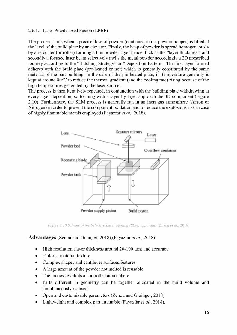
16
2.6.1.1 Laser Powder Bed Fusion (LPBF)
The process starts when a precise dose of powder (contained into a powder hopper) is lifted at
the level of the build plate by an elevator. Firstly, the heap of powder is spread homogeneously
by a re-coater (or roller) forming a thin powder layer hence thick as the “layer thickness”, and
secondly a focused laser beam selectively melts the metal powder accordingly a 2D prescribed
journey according to the “Hatching Strategy” or “Deposition Pattern”. The first layer formed
adheres with the build plate (pre-heated or not) which is generally constituted by the same
material of the part building. In the case of the pre-heated plate, its temperature generally is
kept at around 80°C to reduce the thermal gradient (and the cooling rate) rising because of the
high temperatures generated by the laser source.
The process is then iteratively repeated, in conjunction with the building plate withdrawing at
every layer deposition, so forming with a layer by layer approach the 3D component (Figure
2.10). Furthermore, the SLM process is generally run in an inert gas atmosphere (Argon or
Nitrogen) in order to prevent the component oxidation and to reduce the explosions risk in case
of highly flammable metals employed (Fayazfar et al., 2018).
Figure 2.10 Scheme of the Selective Laser Melting (SLM) apparatus (Zhang et al., 2018)
Advantages (Zenou and Grainger, 2018),(Fayazfar et al., 2018)
High resolution (layer thickness around 20-100 µm) and accuracy
Tailored material texture
Complex shapes and cantilever surfaces/features
A large amount of the powder not melted is reusable
The process exploits a controlled atmosphere
Parts different in geometry can be together allocated in the build volume and
simultaneously realised.
Open and customizable parameters (Zenou and Grainger, 2018)
Lightweight and complex part attainable (Fayazfar et al., 2018).
17
Disadvantages (Zenou and Grainger, 2018),(Fayazfar et al., 2018)
High part residual stresses due to the high thermal gradients generated the process
Relatively slow process in the face of the other AM techniques
Risky user exposure to carcinogenic metal powders (Zenou and Grainger, 2018).
Low build rate
Cavities cleaning is needed to remove the exceeding powder (Fayazfar et al., 2018).
Defectology (Fayazfar et al., 2018),(Debroy et al., 2018)
Over-melting as well as under-melting cause porosity which can promote cracks
initiation (Fayazfar et al., 2018)
Residual porosity due to gas entrapment
Lack of fusion due to an inappropriate source energy set resulting in an insufficient
molten pool penetration of the underlying layer
Cracking and delamination due to the different cooling parameters of the new layer
deposited and the overlaying material already solidified.
Residual stresses and thermal distortions affect the as-built parts (Debroy et al., 2018).
2.6.1.2 Electron Beam Melting (EBM)
The approach used by the EBM apparatus to 3D realise the parts is similar to that exploited in
the SLM technique, although in this case, the primary energy source focalised on the powder-
bed is an electron beam instead of a laser source. Before selectively melting the particles, the
electron beam is de-focalised and made scanning the powder bed with a low energy regime to
pre-sintering the powder. Furthermore, thanks to this adjunctive step, is so possible minimise
the support generation needs conferring a preliminary strength to the pre-consolidated layer
times to sustain it during the forming phase (Zenou and Grainger, 2018).
The process is generally run in low pressure or vacuum conditions with only a small amount of
helium to avoid undesired beam scattering phenomena (Zenou and Grainger, 2018).
The temperatures involved are sensitively higher than that occurring in the SLM. For instance,
during the building process, depending on the type of metal alloy processed, the bed can easily
reach temperatures up to 1000°C. These thermal conditions, due to the high electron energy
source, lead moreover to a medium-low cooling rate, therefore, to modest residual stresses
within the parts.

18
Figure 2.11: Scheme of the Electron Beam Melting (EBM) apparatus (Zhang et al., 2018)
Figure 2.12: Main EBM forming steps (Galati and Iuliano, 2018).

19
Advantages (Zenou and Grainger, 2018)
Modest residual stresses due to the high temperatures involved
Faster than SLM because of thicker layer melted
Suitable to build relatively large components
Reduced need of support generation thanks to the pre-sintering phase giving more
stability to the overhanging surfaces (Zenou and Grainger, 2018).
Disadvantages (Zenou and Grainger, 2018)
Only conductive powders are processable
The necessity to treat residual powder to make it reusable because heat-treated
Alloying elements evaporation can occur because of too meagre vapour tension (Zenou
and Grainger, 2018).
Defectology (Villeneuve et al., 2018)
Tolerances errors and surface defects:
Staircase defect due to layer thickness and part orientation
Not compliant beam positioning
Error in platform positioning
Overhang surfaces warping and curling
Loss of thickness and loss of edge (Villeneuve et al., 2018).
2.6.2 Directed Energy Deposition (DED)
Unlike PBF technologies, the Direct Energy Deposition technique enables to build
functional parts, directly on the base plate, melting the material when it is depositing so
realising in-situ dense parts thanks to the high cooling rate involved which allows a rapid
material solidification (Gibson, Rosen and Stucker, 2014).
More in general, two different subsets of DED technology can be distinguished: the
“Blown Powder” DED system (Powder Feeding), and the “Wire” DED system (Wire
Feeding). These two, differ for the feedstock material form employed to be melted and
welded with the substrate or with the already solidified deposited layers (Gibson, Rosen
and Stucker, 2014). For a more detailed classification of the DED processes, the reader is
reported to Table 1.
.

20
Figure 2.13: Scheme of the Laser Engineered Net-Shaping technique (Zhang et al., 2018)
2.6.2.1 DED-Wire Feeding
The WAAM technique, as a subset of the DED processes, can be furtherly categorised in
three main classes distinguished on the type of energy source that they exploit: “Gas
Tungsten Arc Welding” (GTAW), “Gas Metal Arc Welding” (GMAW) and “Plasma Arc
Welding” (PAW) (Wu et al., 2018).
Similarly to the Blown Powder systems, the deposition by WAAM can occur either in a
sealed chamber with a controlled atmosphere or in the atmosphere employing a shielding
gas system. Furthermore, keeping the parallelism, in both cases, the deposition tools are
driven by robotic arms which guarantee high building freedom. Furthermore, to control the
process performances and the process parameters such as the involved temperatures, the
bead regularity and the material behaviour, the apparatus is equipped with sophisticated
transductors and sensors (Wu et al., 2018).
More specifically, the deposition starts when a laser or an electron beam source melts the
wire feedstock to the substrate realising the first layer (or Single Scan Track as well).
Therefore, the part is realised for successive layers over positions forming a 3D
component. Thanks to the fully dense feedstock material, following an appropriate
deposition strategy, the WAAM technique is generally caple of realising not too complex
3D parts, with no porosity imputable to the process and with a material utilisation of about
100%. For this reason, this technique is broadly used to realise structural and functional
parts as well as for cladding operations. However, even though the lack of porosity within
the part built represents a remarkable advantage in terms of structural performances and
part functionality, the dimensional accuracy and the surface finishing result to be very
meagre. As a result, post-process subtractive operations are fundamental before
implementing the component in its application (Gibson, Rosen and Stucker, 2014).

21
Figure 2.15: General scheme of the Wire Arc Additive Manufacturing (WAAM) technique (Molitch-Hou, 2018)
Advantages (Cunningham et al., 2018), (Gibson, Rosen and Stucker, 2014)
Material utilisation close to 100%
Generally, very meagre porosity (also depending on the material type and the process
parameters)
Possibility to build structural components (Gibson, Rosen and Stucker, 2014)
No powder recovery system required
Cheaper than Blown Powder DED
Capability to process a great variety of materials
Relatively low capital investment for the equipment
Reduced health risk compared to that promote by powder usage
High deposition rate 1-10 Kg/h (Cunningham et al., 2018).
Disadvantages (Gibson, Rosen and Stucker, 2014), (Cunningham et al., 2018), (Greer et al.,
2019)
Inadequacy to realise too complicated parts
Not suitable to implement features with layer thickness transitions
Dimensional and surface finishing inaccuracy (Gibson, Rosen and Stucker, 2014)
Large grains’ growth undesired for room temperature applications
Difficulty in monitoring the “inter-pass temperature” to reduce the heat storage within
the part
Difficulties in obtaining fine microstructure (Cunningham et al., 2018)
Machining always needed to release support structures (Greer et al., 2019)

22
Defectology (Wu et al., 2018), (Cunningham et al., 2018)
High residual stresses and cracking whether a poor deposition pattern is
implemented
Thermal deformation due to high heat storage within the part
High-temperature fatigue
Severe oxidation fo Ti-alloys
High residual porosity for Al-alloys
Low surface finishing and dimensional distortions for Steel (Wu et al., 2018)
Micro fissures
High anisotropy
Surface waviness (Cunningham et al., 2018)
2.6.2.2 DED-Powder Feeding-LBMD
The apparatus typically consists of the main nozzle mounted into a two- or three-axis
mechanic arm system, in which is embedded the primary energy source; this latter is either
an Nd-YAG or CO2 laser, or an electron beam. The building plate is tight to a separate
mechanic system which makes its motion viable in two- or three-axis and independent to
the nozzle’s motion. Therefore, the high mobility of the primary mechanic arm and the
base plate, allow in the overall to build the part with up to nine freedom degrees (Zenou
and Grainger, 2018).
Besides, in order to monitor and optimise the deposition, the system is equipped with an
“integrated feedback system” recording and analysing the data of the ongoing deposition
process. Through apposite sensors detecting the light in the deposition zone (infrared
cameras or pyrometers (Thompson et al., 2015) ), the open parameters, such as laser power
and scan speed, can be retroactively handled to optimise the deposition (Mazumder, 2017).
Furthermore, it is also possible to couple the DED technology with a CNC apparatus,
therefore, creating a hybrid system able to perform additive and subtractive operations
simultaneously [31].
Thanks to this latter capability, this type of technology allow repairing damaged parts
adding material to an already existing part and subtracting the exceeding one in order to
control the dimensional allowances and the surface finishing. Is moreover possible, to
realise surface coatings employing a multicomponent feedstock.

23
Figure 2.14: Scheme of the Laser Beam Metal Deposition (LBMD) technique - a) coaxial nozzle feeding, b)
single nozzle feeding (Gibson, Rosen and Stucker, 2014)
More in detail, the layers deposition is performed by a “deposition head” embedding a
feeding system composed by one or multiple channels, fluxing a mixture of metal powder
and carrier gas in conjunction with shielding gas. This latter is fundamental to prevent the
impurities embedding, as well as the material oxidation, whether the deposition is
performed in the atmosphere. The channels just described face to the centre of the tool
conveying the blend of powder and gas towards the laser beam focused in the central zone
of the head.
When the laser source interacts with the plate, the substrate melts creating a “Melt Pool”
in which the fluxing particles become entrapped. Depending on the “open” process
parameters set, the particles can be either melted in flight before they reach the Melt Pool
or else when they enter within the melt pool itself. Commonly, this later instance is that
one typically adopted (Gibson, Rosen and Stucker, 2014).
However, not all the powder fluxed towards the building zone is exploitable by the process
since part of it ricochets on the substrate without interacting with the molten material.
2.6.2.2.1 Process parameters - LBMD (Powder Feeding)
Since the LBMD process is at open parameters, it is possible to effectively and accurately
manage the same to optimise the deposition, so manufacturing complex parts endowed
with particular mechanical, geometrical and functional properties.
As a matter of the fact that the as-built part’s properties are tightly related to the process
parameters setting, the “Transverse Speed”, “Laser Power”, “Feed Rate”, “Powder
Stream” and “Hatching strategy” play a fundamental role influencing the cooling rate, the
part geometry and the surface finish, besides the mechanical properties hence, the
microstructure.

24
(Transverse speed)
As the process starts, the primary energy source melts the substrate, so creating the Melt
Pool, semicircularly shaped in its cross-section, with dimensions in the range of 0,25-1mm
in diameter and 0,1-0,5 mm in depth (Gibson, Rosen and Stucker, 2014).
From a physical perspective, as the deposition head is spatially displaced, the dynamic
deposition of the material can be interpreted as the Melt Pool’s elliptical trailing, moving
at a velocity set. Therefore, it appears clear that the transverse speed, or else the deposition
head velocity (typically ranging between 1-20 mm/s), directly affect the tracks’ profile and
width, beside the productivity rate. Nevertheless, selecting the appropriate Trasverse speed
value, it must also be considered its correlation with the cooling rate, which as already said
influences the microstructure (Thompson et al., 2015).
Furthermore, in order to achieve a homogeneous deposition, the Laser Power “P” must be
increased together with the deposition speed, to properly melt the amount of flowing
particles fluxed in the unit of time. As a result, a severe increase of these two parameters
entails to very high-temperature gradients spread out in a heat-treated zone, in conjunction
with a very brief time given to the molten material to cool down.
Therefore, the transverse speed directly affects the Melt Pool’s cooling rate (generally
ranging in 103 – 105 °C/s) hence the microstructure’s morphology and properties (Gibson,
Rosen and Stucker, 2014).
For instance, a high transverse speed leads to high cooling rates promoting a fine and
columnar grains’ growth, whereas, modest transverse speed values produce low cooling
rates responsible for a coarse microstructure (Shamsaei et al., 2015).
(Laser Power)
Aside from the transverse speed, the cooling rate is also affected by the molten metal
superheating as a consequence of the Laser Power level employed (generally it varies in
the range of 100 – 5000 W (Thompson et al., 2015)). Inversely to the Transverse speed, a
high Laser Power level promotes a coarse microstructure whereas modest laser energy
leads to fine and columnar microstructures. However, to undertake an accurate analysis of
the deposition performances, the nominal P-value it is not sufficient to accurately define
the fusion results. It is indeed necessary to consider the real energy absorbed by the
material, not taking into account the radiation reflected by the substrate or by the deposited
material as well (Shamsaei et al., 2015). A deepening on this point is provided in section
2.6.2.2.1 when dealth with the “Specific Energy”.
(Flow rate)
Definable as the mass of powder fluxed by the nozzle(s) in the unit of time, the powder
feed rate (g/min), directly influences the deposition homogeneity and compliance
(Mahamood and Akinlabi, 2018).
Since its conception, when the laser cladding technologies have been introduced, it
represents one of the most challenging parameters to be handled because of the difficulty
to make this parameter predictable. Although the major part of studies and applications
consider the feed rate as a constant variable, according to Lie Tang et al. a better strategy
to achieve a uniform and homogeneous deposition, is to consider the flow rate as a dynamic
parameter. According to that, it is indeed possible to take into account the deposition head
accelerations and deceleration occurring during the deposition process, thanks to a control

25
system termed “Variable powder flow rate control” (VPRC) based on optoelectronic
sensors (Tang et al., 2008). In particular, high flow rate (generally ranging between 1 – 10
g/min) values result in an increased melt pool density due to the significant amount of
particle mass fluxed in the same unit of time besides providing an enhanced layer
thickness. However, the flow rate effectively influences the deposition accordingly to what
just stated only at relatively low Laser Power levels, whereas, for high energy values
employed, its effect is meagerly recordable (Thompson et al., 2015),(Shamsaei et al.,
2015).
Furthermore, it results important also to optimise the relationship existing between flow
rate and transverse speed, for instance, running custom software analysis before the
deposition process in order to avoid feeding breaks or else drawbacks.
(Laser beam and powder stream)
Together with the influence of the singles exposure parameters, it must be considered their
dynamic coupling. In fact, since the powder stream and the laser beam coupling can be not
considered as fixed, the nominal values do not represent unique data to optimise the
deposition. Nevertheless, different head deposition orientations affect the powder stream
percentage effectively interacting with the laser beam and then with the dynamic Melt
Pool. Different Laser Beam - Powder Stream coupling configurations can indeed arise
during the process depending on the 3D path that the deposition head follows to realise the
component and on the equipment settings(Figure 2.15). For instance, if the deposition head
is inclined to the horizontal, the powder stream can be subjected to the gravity effect and
easily be deflected downwards decoupling in part from the area of laser interaction.
Therefore, as a consequence of an optimised interaction or not between laser source and
powder stream direction, different layers’ height and boundary conditions are achieved at
the deposition end (Shamsaei et al., 2015).
Figure 2.15: laser beam and powder stream dynamic configurations.
(Hatching Strategy)
With “Hatching Strategy” it is intended the repetitive pattern followed by the nozzle when
depositing the material in a 2D area. How the layers are successively deposited and overlapped,
largely influences the residual stresses, the thermal distortions, the eventual part deflection and
the porosity morphology and percentage within the final part. According to that, the Hatching

26
strategy must be designed with the intent to minimise and avoid these drawbacks as more as
possible (Shamsaei et al., 2015).
Although a great variety of them exists seeing its “open” nature, the scan patterns to choose
from and broadly employed are commonly four: “Raster”, “Bi-directional”, “Off-set” and
“Fractal”. The scan pattern often preferred among these, thanks to its easiness to be
implemented and its high adaptability to be employed independently from the part’s shape, is
the Raster pattern. However, the “Off-set” and the “Fractal” patterns, even though generally
less exploited, ensure an enhanced geometrical accuracy in conjunction with an energy
consumption saving. Furthermore, these latter have been found to provide the lower substrate
deformations after the part’s cooling (Shamsaei et al., 2015).
Figure 2.16: Different scanning strategies: a) Raster, b) Bi-directional, c) Off-set out, d) Off-set in, e) Fractal
(Shamsaei et al., 2015)
2.6.2.2.2 Parameters correlation
According to what just reported in the description of the specific parameters, it is
fundamental to notice how they are interrelated one to each other. Therefore, to pursue an
optimal and homogeneous deposition, it results necessary to rationalise the mutual
influences of Laser Power, Feed Rate and Transverse speed in combined parameters. The
two here deemed as essential and as the starting point on which base a deposition
optimisation are: the “Specific Energy” and the “Powder Feed Density” (Shim et al., 2016).
(Specific Energy)
Wanting to determine the optimal process parameters value, so that is possible to ensure a
proper material melting beside a prediction of the layer height/width ratio, it has to be
considered the “Specific Energy E” (J/mm2). This latter, correlates the Laser Power P (W),
the laser spot diameter d (mm) and the transverse speed v (mm/s) as reported just below in
the Equation (2.1)
𝐸 =𝑃
𝑑𝑣 (2.1)

27
This parameter defines the optimal energy value, thresholding in its lower limit, a lack of
fusion and in its upper limit a too high dissolution (Shim et al., 2016).
(Powder feed density)
Otherwise, the powder feed density correlates the Feed/Flow Rate with the laser spot
diameter and the transverse speed, instead of the laser power. The Powder feed density F
(g/mm2) is defined as follows in Equation (2.2) where G is the Powder Flow Rate (g/min),
d the laser spot diameter (mm) and v the Transverse speed (mm/min) (Shim et al., 2016).
𝐹 =𝐺
𝑑𝑣 (2.2)
(Layer thickness calculation)
As already mentioned, it is possible to highlight a direct correlation respectively between
the laser power and the feed rate with the layer thickness. As a consequence, it can also be
noticed the direct relationship with the layer thickness and the Specific Energy and the
Powder feed density as well. Therefore, is finally possible correlate all the exposure
parameters previously analyzed with the layer thickness “t” (mm) as parameter
representative of the crucial and primary feature of an optimal deposition, thanks to the
implementation of the two combined parameters “E” and “F” respectively in the two
experimental equations (2.3) and (2.4) (Shim et al., 2016).
𝑡 = 12.64 + 2.55𝐸 (2.3)
𝑡 = 22.85 + 2.75𝐹 (2.4)
(Deposition optimisation Map)
To complete the framework of the process parameters correlation, is here just below drafted a
typical process map considering the Laser Power and the Scan velocity as reference
parameters. These maps intend to display a safety region in which run the deposition to avoid
the defectology occurring.
Figure 2.17: Deposition optimisation map for a DED process, safety window and main defectology categories
(Sames et al., 2016).

28
Advantages (Molitch-Hou, 2018), (Zenou and Grainger, 2018), (Zhong et al., 2019),
(Gibson, Rosen and Stucker, 2014)
Possibility to repair damaged components
Very high productive rate compared to that of PBF
It is possible to dispose of hybrid DED – CNC apparatus (Zenou and Grainger,
2018).
Employable for surface modification and laser cladding
Very fine microstructure due to the high cooling rate (Zhong et al., 2019)
Possibility to build very large components
The deposition is performable with multiple degrees of freedom, thanks to the
multi-axis motion of the deposition head as well as of the build plate (Molitch-Hou,
2018).
Capability to deposit multi-component materials (in-situ composites)
Microstructural control thanks to the mixture and cooling rate handleability
Solidification direction control and monocrystal manufacturability (Gibson, Rosen
and Stucker, 2014)
Disadvantages (Najmon, Raeisi and Tovar, 2019), (Zenou and Grainger, 2018), (Zhong
et al., 2019), (Gibson, Rosen and Stucker, 2014)
High residual stresses in the as-built part
Whether the apparatus includes a sealable chamber, a large amount of inert gas
(Nitrogen or Argon) is required in conjunction with an appropriate lead time to
reach the oxygen level desired.
Poor resolution and surface finish
Accuracy not better than 0.25mm and surface finish at least of 25 µm
Supports removal needed (Gibson, Rosen and Stucker, 2014)
Anisotropy especially employing the WAAM technology (Najmon, Raeisi and
Tovar, 2019)
Are often required further finishing operations such as machining, in order to
control the dimensional allowances and the surfaces features (Zenou and Grainger,
2018).
Generally limited deposition rate in the range of 0.5 Kg/h (Zhong et al., 2019)
Defectlogy (Gibson, Rosen and Stucker, 2014), (Thompson et al., 2015)
Cooling rate changing can occur especially in thin-walled structures
Cracking due to residual thermal stresses
Cracking and delamination occurring as a consequence of repeated thermal cycles
Porosity and balling effect in case of not optimised process parameters (Gibson,
Rosen and Stucker, 2014).
Porosity due to gas entrapment
Irregular deposition due to powder stream not correctly aligned
Lack of fusion in case of not optimised process parameters (Thompson et al., 2015).

29
2.6.3 DED and PBF comparison The two primary metal A.M. categories are compared in their main hallmarks as follows, taking into considerations their three main LMD, SLM and EBM subcategories.
Table 2: General differences of process parameters and equipment capabilities between LMD, SLM and EBM
(Zenou and Grainger, 2018),(Thompson et al., 2015),(Gibson, Rosen and Stucker, 2014) (Zhong et al., 2019).
LMD SLM EBM
Nd-YAG or CO2 laser
(100 – 5000W)
Ar/He shielding gas
Powder preheating not
necessary
Base plate preheating
No build size limitations
Melt Pool size width
0,25-1mm
Layer thickness 100-
200µm
Surface finish > 25µm
Geometric tolerance ±
25 mm
Building rate ~ 0,5Kg/h
Repairing
Generally lower
mechanical properties
than SLM and EBM
(coarser microstructure)
One or more fibre laser
(200-1000W)
Ar/N2 atmosphere
Powder preheating at
100-200⁰ C
Base plate preheating
Build size limited by the
chamber volume (ex.
500x350x300 mm3)
Melt Pool size width 0,1-
0,5
Layer thickness 20-
100µm
Surface finish 4-11 µm
Geometric tolerance ±
005-0,1 mm
Building rate ~ 20/35
cm3/h
No repairing
High power electron
beam source (up to
3000W)
Vacuum/He
atmosphere
Powder pre-
sintering at 700-
900⁰ C
Base plate preheating
Build size limited by the
chamber volume
Melt Pool size width 0,2-
1,2
Layer thickness 50-
200µm
Surface finish 25-35
µm
Geometric tolerance ± 0,2
mm
Building rate ~ 80 cm3/h
No repairing

30
2.7 Metal AM Applications
Although the Additive Manufacturing has been mainly tought as a Rapid Prototyping
technique so far, a clear trend to turn this technology into a convenient and sustainable
manufacturing process is nowadays evident.
In the face of all the markets branches, the Aerospace/Aviation, the Automotive and the
Bio-medical fields, are indeed the main sectors driving the AM advancement in
conjunction with specialised companies and the academia.
(Aerospace/Aviation)
Dealing with the Aviation and the Aerospace field, the AM finds a role in manufacturing
functional and structural components, for rapid tooling and rapid prototyping, and for
repairing operations as well.
The AM success in this field is imputable to its remarkable flexibility and its capability to
break down several constraints affecting the traditional manufacturing processes.
Furthermore, complementarity between the aerospace components requirements and the
AM distinguishable features can be recognised. To clarify this perspective, a parallelism
between the aviation components needs and the AM hallmarks acts to satisfy them is
reported in Table 3 (Liu et al., 2016).
(Automotive)
Likewise, in the Automotive field, the costs and weight reduction, represent the most
modern binding challenge that all automotive companies are facing.
At this purpose, these are applying and extending the number of AM applications seeing
the 3D printing capability to manufacture sophisticated, light-weight and functional parts
(Singh and Singh, 2017).
Relatively to short production runs, is in this way possible cut off costs and lead times.
Also, the freeform fabrication techniques allow a without precedents parts customisation;
this latter feature critical to differentiate the product in a full field, where the competition
is fierce.
(Bio-Medical)
The main AM distinguishable feature of which the Bio-Medical sector benefits, is the
capability to conceive and realise tailored components. Is indeed possible, to realise
prosthesis as well as scaffolds, in multi-material and with variegated textures in the same
object. Nevertheless, the studies concerning the possibility to employ metallic materials
appointed to be used in the Bio-Medical sector, have led to outstanding results. Nowadays
it is not unexpected realise 3D parts in a great variety of metals and alloys such as titanium
alloys (such as Ti–6Al–4V), Co-Cr alloys, Inconel, stainless steels, aluminium, hard and
amorphous metals, copper, niobium and beryllium (Singh and Singh, 2017).

31
Table 3: Aerospace components requirements vs Additive Manufacturing contextual hallmarks
2.7.1 DED Aerospace/Aviation Applications
The DED system can process varied types of metallic materials of Aerospace/Aviation interest,
such as titanium, Inconel, stainless steel, aluminium and their alloys. Furthermore, it is also
possible to produce functional components or coatings as well, with graded materials, charging
different powder types in the separate hoppers; hence, fluxing them by different nozzles.
Furthermore, since the DED apparatus can be coupled with a CNC unit in a hybrid machine, it
is possible to realise parts in multiple exploiting different axis of work, performing additive and
Avio - Aero requirements
AM contextual hallmarks
Complex geometries and high
envelope to volume ratio (Liu et al.,
2016)
Freeform fabrication capability (Liu et
al., 2016)
Difficult machinability & buy-to-fly
ratio (Liu et al., 2016)
Capability to process advanced and
hard materials such as Ni-, Ti-, special
steel- alloys with very high material
utilisation (Liu et al., 2016)
Small production runs (Liu et al.,
2016)
No tools need resulting in cost-saving
and high process competitiveness for
small quantitative (Liu et al., 2016)
Quick turnaround parts (Liu et al.,
2016) and lead time reduction
Fust on-demand production
High strength-to-weight ratio,
resistance at high temperatures,
fatigue loads and aggressive
environments (Liu et al., 2016)
High parts customisation (Liu et al.,
2016) and parts topologically
optimizable to reduce weight
Generally improved mechanical and
microstructural properties respect to
wrought components
Real-time cooperation with the
decentralised manufacturing plant
Remote manufacturing capability

32
subtractive operations as well. Thanks to this versatility, hollow and complex parts embedding
functional features, such as channels times to create a cooling system or thin wall structures as
well, can be built without supports generation. The CNC unit can be moreover used to control
the surface finish and the dimensional allowances spending an overall process time, ten times
lower than that required from a PBF process with subsequent finishing operations. Finally, only
the DED technology can overhaul damaged components otherwise from PBF and all the other
metal AMTs (Liu et al., 2016).
(DED Applications examples)
Wanting to report some applicative examples, a thin-walled helicopter engine combustion
chamber (300 x 90mm) built of IN718 by LMD, is indicated in Figure 18. More specifically,
the component has been realised with a 0.9 Kg/h deposition rate achieving a 99.5% of density
throughout the part in remarkably short time-lapse of around 7.5 hours rather than in months.
Furthermore, two Ti-6Al-4V airfoils embedding cooling channels (Figure 2.19) have been
successfully realised by LMD at the International Institute of the National Research of Council
in Canada (Liu et al., 2016).
Finally, the main repairing steps of a turbine housing realisation employing a hybrid system has
been reported as follows (Figure 2.20). As the sequence of the shots depicts, is possible to 3D
print the component and then milling its surface to achieve the desired roughness value besides
performing precision subtractive operations to control the dimensional allowances and to
introduce new features. Noteworthy, are also the large component dimensions (180x150 mm)
and the total realisation time of around 5 hours to obtain the finished part (Liu et al., 2016).
Figure 2.18: Helicopter engine combustion chamber built by LMD (Liu et al., 2016)
Figure 2.19: Ti-6Al-4V airfoils built by LMD (Liu et al., 2016)

33
Figure 2.20: Turbine housing building employing a hybrid Additive - Subtractive apparatus (Liu et al., 2016)
2.7.2 Design philosophies and Repairing
As for most of the technological fields, the advancement of the air/space-craft structural
safety has been pursued and Implemented throughout the years, thanks to a trial and error
learning approach. Unfortunately, some remarkable improvements in this ambit have been
promoted by air incidents that have led the engineers to understand the causes and to adopt
the appropriate countermeasures (Alderliesten, 2018).
“Safe life”
The first and more ancient perhaps design philosophy adopted by the aircraft designers is
the “Safe-life”. According to this approach, it was assumed that a structure maintains its
integrity throughout its life independently from the environmental conditions, fatigue
phenomena, accidental bumps and all related matters. Therefore, designing accordingly
such philosophy meant to run a load analysis and over-dimensioning the components, only
considering an appropriate “safety factor” (enlarging the part life), (Figure 2.21) fixing a
retiring point in which the aircraft was decommissioned to be restored. However, this
approach did not guarantee a costs optimisation and a lowering in the buy to fly ratio.
Therefore, as the service life was increased aiming to reduce flights cost, the risk of failures
dramatically increased because of not considering the deleterious effects of the fatigue and
corrosion phenomena besides the presence of defects within the components (every time
present after their manufacturing) potential cracks sites and initiators. (Alderliesten, 2018)
“Life-Safe”
As a consequence of repeated aircraft incidents, new design philosophy was developed.
Wanting to increase the safety of the structure, was adopted the principle for which the
primary structural components were made redundant so that possible damage or excessive
load could be redistributed in the other counterparts. Therefore, a range of tolerance in
terms of operational time in which the aircraft could continue to fly was introduced.
Otherwise, from the Safe-life design philosophy, the new “Life-safe” concept, considered
to keep in flight the plane before its restore even when partial damage or failure occurred
(Alderliesten, 2018).
However, also this second design philosophy presented applicative constraints. Even
though the loads' repartition provided advantages in the overall, it was not taken into
account the Multiple Site Damage (MSD) occurring. This eventuality occurred indeed

34
when the first “homologue” feature failed; hence, the whole load amount was divided
among the other ones. When the features did not sustain the load left, the fatal component
failure, speedily occurred (Alderliesten, 2018).
Figure 2.21: Safe-Life design philosophy (Alderliesten, 2018)
“Damage Tolerance”
As a response to the Safe-life and Fail-Safe philosophy lacks, was introduced a new design
concept considering the strength of both of them so representing a trade-off between the
same.
Since 1978, the FAR/JAR adopted the “Damage Tolerance” as design philosophy (Figure
2.22). This latter takes into account that, the manufactured components, owned
unavoidable impurities and defects as a result of the process-induced chemical-physical
phenomena. Also, it considers at the same time the operational, environmental and
incidental conditions in which the parts have to withstand when in operation, so expecting
the occurring of failure. With this perspective, a program scheduling the maintenance and
repairing operations to restore the damaged parts was adopted (Alderliesten, 2018).
More specifically, a component is designed “damage tolerant” whether it is capable of
sustain loads in conjunction with fatigue, accidental bumps/damages, corrosion and all
related matters, before a scheduled inspection and eventually a repairing operation. In the
case of damaged overhauled parts, repairing operations are run recovering the initial
component strength and extending their operational life (Alderliesten, 2018).
Figure 2.22: Damage Tolerance design philosophy (Alderliesten, 2018), Dark blue line: addition of a Repairing
scenario.
According to the importance of restore wore and damaged parts, in the next paragraph will
be described what the Additive Manufacturing role in this framework is, how it proposes
itself as an excellent alternative to the conventional repairing processes and what are the
main operational steps to be followed. Some applicative examples will also be provided to
the reader.
35
2.7.3 Hybrid Additive and Subtractive Manufacturing systems for repair
As widely known, one of the primary AM constraints is represented by the expensiveness
of the components built. The economic advantages achievable replacing traditional
manufacturing with AM, are mainly limited to some specific applications. More in general,
the AM represents an optimal trade-off between costs and complexity of parts built, when
short runs or limited editions as well, are required.
Another preliminary requirement for which AM could be deemed as suitable to be
employed is the need to create parts for very demanding fields where mechanical
properties, part durability and accuracy are essentials. According to this scenario, is,
therefore, reasonable to think that this type of processes is overlying to frontiers very hard
to be overcome.
However, is nowadays possible to perform parts repairing by Hybrid LMD-CNC apparatus
extending the components life conceiving a productive chain that considers building new
functional components by DED, as well as by PBF, and repair them with hybrid DED-
CNC equipment when damaged. Thereby, with this conception of 3D manufacturing-
repair chain, is hence possible to repair very costly damaged components instead of
replacing them, so sensitively reducing costs and lead time (Liu et al., 2016). Furthermore,
according to some studies run “3D repairing” would also lead to lowered emissions and
modest environmental impact (Najmon, Raeisi and Tovar, 2019).
Otherwise from others repairing conventional processes, such as tungsten inert gas
welding, plasma transferred arc welding, electron beam and plasma spraying, these DED
based Hybrid machines allow to induce less component distortion and more deposition
control with unique simpler equipment. (Liu et al., 2016). More in detail, the best
advantages in terms of deposition precision and material flexibility are recognisable to the
DED Blown Powder technologies which overpass the Wire feeding DEDTs for what
concerns the repairing operations and the implementation of new features in already
existing parts (Gasman, 2019). Besides, the resulting Heat Affected Zone induced by a
DED process such as LMD is remarkably lower compared to that generated in the others
processes aforementioned due to the low energy input heat provided by the AMTs (Liu et
al., 2016).
Repairing Process:
According to R.Liu et al., three different steps of the repairing process are distinguishable
(Figure 2.23). Firstly, a “Repair preparation stage” is run in order to analyse and define the
damage morphology and entity. Therefore, since it is possible to interpret the defect as a
digital file finally, the damage is measured by either contact tools (feelers or touch-trigger
probes) or by non-contact instruments (camera, laser sensors). As a consequence, the
defect “negative” area is extrapolated comparing the data acquired to the first component
area included in its 3D file. In this step, some evaluations on the repairing process
feasibility in order to prevent nozzle collisions, blind areas and so on, are moreover made.
Secondly, the material deposition by AM and the subtractive operations to control the
dimensional and geometric allowances, are performed. Finally, in the third step is taken
into account an analysis of the allowances and compliance, besides, perform
microstructural characterisations and fatigue tests (Liu et al., 2016).

36
Figure 2.23: AM-CNC Hybrid repairing process main steps (Liu et al., 2016).
Figure 2.24: Hybrid AM-CNC apparatus (Liu et al., 2016).

37
(Case studies)
Referring to paragraph 2.7.2 is preliminary to say that not all the aerospace or aviation
components as well, are designed a damage tollerance philosophy accordingly. Parts not
subjected to critical environmental conditions, repetitive loads or not exposed to incidents
can be easily designed following either a safe-life or a fail-safe approach. The same design
strategy is adopted for components not easily attainable from the maintenance operators;
therefore in these instances, an appropriate safety factor and controlled primary and
secondary manufacturing operations are essentials.
However, in this paragraph are presented some representative examples of aviation
components underlying to a damage tolerant design due to their operational functions and
conditions.
A climax example for which the technology just described could be suitable for, is the
turbine blades repairing. Metaphorically, we could also extend this application to turbine
rotors repairing which embed a single blades row, otherwise termed “blisks”. As a turbine
blade is damaged, it releases debris that affects the other blades and the whole component
integrity. An example of blades leading edge repairing by LENS of a compromised Ti64
blisk, is depicted in Figure 2.25 (Liu et al., 2016).
Another example of Avio component restore is reported according to the study run by Xue
and Islam work, in which it has been possible to repair an IN738 turbine blade presenting
a relevant lacking portion of its tip by LMD (Figure 2.26) (L. Xue, 2006).
Figure 2.25: T700 blisk repaired by Optomec LENS (deposition) and by CNC (finishing) (Liu et al., 2016).
Figure 2.26: IN738 Turbine blade repaired by LMD (L. Xue, 2006).
38
2.8 Ni Superalloys and AM
Commonly, the Ni-“Superalloys” are defined as a subset of the metallic alloys, that according
to a general classification provided by Kevin Minet et al., can be formulated as Iron-Nickel
based or Cobalt-based or Nickel-based (Minet et al., 2019).
Their first introduction to the market dates to the ’40s during World War II, where this new
class of advanced materials were employed to manufacture jet engines as well as military gas
turbine components. Successively, in the ‘50s – ‘60s the superalloys development and usage in
fields such as high-temperature helium reactors, heat exchangers, furnaces, sour gas implants
and obviously in aero engines and gas turbines, soared. Otherwise, the superalloys
manufacturing processes improvement caught on lately in the 70s–80s. As a result, the new
manufacturing techniques, led to the new possibility of the alloys chemical design, besides
several productive advantages. For instance, thanks to the introduction of new processes to
manufacture single-crystal components, the employment of Mo, W and Ta to promote carbides
formation resulted obsolete. Their presence times to strengthen the material acting as pinning
particles for the dislocations at the grain boundaries was in this instance inutile (Sims, 1984).
Although new manufacturing processes allowed to influence the Superalloys chemical
composition, their microstructure is still very complex and characterised by varied elements
and phases. Nevertheless, this complexity of phases and microstructures is what makes these
types of materials so outstanding.
More precisely, the most significant Superalloys’ hallmarks that in the overall made them so
precious and suitable to fulfil the design needs of very demanding sectors, as the Aviation and
Aerospace are, can be listed as (Minet et al., 2019):
their capability to withstand under very high temperature keeping their mechanical
resistance untouched up to around 80% of their melting temperature
their enhanced oxidation and corrosion resistance (Minet et al., 2019).
Wanting to address better the main issues related to the synergy intercurrent between material
and process, it must be considered that even though the “new” casting processes introduced
around the ’80s brought essential advantages, the today market needs present in some instances
obstacles hardly surmountable by them. Conversely, the metal AMTs are nowadays the driving
force pushing forward the manufacturing, when highly performant, tailored and sophisticated
components are demanded. About the materials availability, even though initially the Ni-
Superalloys have been formulated accordingly casting needs, it is nowadays possible to dispose
of a significant variety of superalloys for AM to produce and repair complex components such
as turbine blades in IN738 or MAR-M247 by A.M (Minet et al., 2019).
Furthermore, as the Ni-Superalloys born and developed relatively to the gas/Jet turbines, Figure
2.27 shows the various components for which these advanced materials can be used.
However, before describing how the metal AM comes into play processing the Ni-Superalloy
and with what results, is reported in the paragraphs as follow a summary of the main phases
and microstructural elements characterising a Ni-based superalloy.

39
Figure 2.27: Jet Turbine engine section depicting some fundamental components and indexing the materials
with which they are manufactured (Minet et al., 2019)
2.8.1 Microstructure description and Phases
Although, the superalloys chemical composition is variegated and complicated because of the
large number of chemical elements present, it can be said that all Superalloys Ni-based share a
primary Face Cubic Centered (FCC) ɤ phase. Otherwise, the Iron and Cobalt-based Superalloys
commonly owns a body-centred Cubic (BCC) lattice at room temperature. However, also, this
latter can preserve an Austenitic FCC phase in the case of Ni- is present within the alloy’s
chemical composition (Minet et al., 2019).
Starting from the first thirty years of the 20th century, several studies have been run on the
Superalloys’ microstructure in order to optimise and better understand their chemical
composition.
In the years 1929-1930, adding aluminium and titanium the new “age hardening”, the cubical
and coherent phase ɤ’ Ni3(Al, Ti) was discovered (Figure 2.28). Thus, firstly introduced in the
“Nimonic 80”, in the “Tinidur” and in the “A-286” Ni-based Superalloys, presented an FCC
austenitic structure providing a strengthening effect when in coexistence with the ɤ matrix.
However, it was early discovered that the strengthening effect could be achieved only whether
the Ti and the Al adding happened simultaneously. Otherwise, in the presence of only Ti added,
a deleterious plates structure to strength was generated. Successively, in the late ‘50s, the further
strengthening FCC two cubes stacked secondary phase ɤ’’, was discovered by “Eislestein”
during its compositional experiments concerning the IN718 Superalloy (Sims, 1984).
Nevertheless, ɤ’ and ɤ’’ was not the only peculiar phases discovered and of which the
metallurgists benefitted. It was also taken advantage from M23C6, M6C and MC carbides
formation, which provided strengthening either by heat treatment or by the formation of
adjunctive ɤ’ thanks to the MC interaction with the ɤ matrix, the former acting as sumps

40
providing carbon for the phase transformation. As the representative of this latter case, is here
just below reported the reaction expression (5) (Sims, 1984).
MC + ɤ MC23C6 + ɤ’ (5) (Sims, 1984)
Furthermore, in the same ‘50s, the M23C6 were also discovered to be as dispersed phases within
the gamma matrix, acting like bonding agents between different grains, therefore, creating a
further strengthening configuration. However, around 1970 was discovered the far better
Hafnium strengthening effect. The Hafnium addition, promoted indeed a contort grain
formation hence, generating a grains interrelated network that physically made obstruction to
the displacement of the components (Sims, 1984).
With the advent of the ’60s, the Oxides dispersion strengthening (ODS) were introduced as
promoters of improved creep resistance. With the oxides insertion of ThO2 and Y2O3, was hence
possible to keep the superalloy’s mechanical properties unchanged up to approximately 80-
90% of the material’s melting temperature. Another method adoptable wanting to improve the
superalloys mechanical properties, instead of modifying its chemical composition, is to promote
a rapid and directional solidification. In this way, it was indeed possible to create fibrous
eutectic phases starting from TaC, M23C6 and δ-phase reserves. Moreover, a rapid cooling was
discovered to be an optimal means to suppress deleterious phases such as σ-phase, µ-phase and
Laves-phase besides to induce a directional grain growth. These, have been indeed dreaded
from the metallurgists because of their brittleness and plate shape, inducing cracks formation
whenever the component was subjected to creep conditions (Sims, 1984).
Figure 2.28: Main Ni-based superalloy phases throughout their years of discovery (Sims, 1984).

41
Figure 2.29: ɤ’- FCC Bravais lattice (Minet et al., 2019).
(Superalloys strengthening mechanism and classification)
Generally, the remarkable Superalloys capability to withstand at high temperatures and hostile
environments, preserving their mechanical properties is mainly due to two strengthening
mechanisms (Minet et al., 2019):
Strengthening by solid solution of the ɤ matrix
Hardening by precipitation of the ɤ’ Ni3(Al, Ti) and the ɤ’’ Ni3(Nb) phases (Minet et
al., 2019)
2.8.2 Strengthening by Solid Solution
As reported in Table 4, a great variety of alloying elements can be present in Ni-based
superalloys. According to that, a substitutional solution can occur, leading some chemical
elements to substitute the matrix atoms in their lattice position. As a result, around these lattice
positions, because of the mismatch between the “hosts” atoms and the matrix atoms radii, a
strain field interacting and making obstruction to that of the passing dislocations during plastic
deformation, is generated. Furthermore, a further strengthening effect is also provided when the
substitutional elements have a higher Young’s modulus respect to that of the matrix. This
strengthening phenomenon generally concerns the ɤ matrix rather than the ɤ’ phase because of
its highly ordered microstructure (Goodfellow, 2018).
2.8.3 Hardening by Precipitation
Another strengthening mechanism is the ɤ’ phase precipitation. While the dislocations
displacement quite easily deforms the disordered ɤ matrix, higher energy is required to them in
order to alter the ordered ɤ’ precipitates lattice. Depending on the precipitated particles’ size,
two different phenomena occur (Goodfellow, 2018).
In the case of small ɤ’ particles, the same are traversed in two different moments by a couple
of two different shearing dislocations: a “leading” and a “trailing” dislocation. As the first
interacts with the ɤ’ lattice, the Al atoms replace the Ni ones in their lattice positions, entailing
to an energy increase as a result of a bridging zone between the two dislocations (termed as
Anti-phase region), creation. After that, the first is passed, the trailing dislocation traverses the
Anti-phase region restoring the initial lattice order. This phenomenon responds to the name of
“Weak pair coupling” (Goodfellow, 2018). Otherwise, because of the higher Anti-phase

42
boundary energy (APBE) present in large particles subjected to shearing forces, the trailing
dislocation interacts with the precipitates Anti-phase before that the leading one leaves. This
latter phenomenon is defined as “Strong pair coupling” (Goodfellow, 2018). However, it is not
unambiguous to determine which mechanism offers a higher strengthening effect. For instance,
in the case of the supersolvus IN100 alloy, small precipitates entail to higher yield strength than
that achievable with larger ones.
On the other hand, the trend is reversed in the instance of subsolvus IN100, where the presence
of large ɤ’ particles provides a strengthening effect superior to the supersolvus case. Finally,
concerning overaged alloys, therefore characterised by very large particles (around 1 µm), an
Orowan strengthening mechanism is also possible even though rarely present in Ni-based
superalloys because of meager values of mismatch intercurrent between the precipitates and the
matrix (Goodfellow, 2018). Finally, it is essential to specify that the two mechanisms just
exposed are only the two considered as owning a most relevant impact on the superalloy
properties. Several further mechanisms such as stacking faults, modulus and chemical
strengthening, grain boundary strengthening and coherency strengthening provide their
contributions to increase the yield strength. However, in the instance of Ni-based superalloys,
the contribution of the stacking faults and the chemical-modulus strengthening can be
considered negligible, whereas the coherency and grain boundary action are considered not as
efficient as the two main mechanisms just reported (Goodfellow, 2018).
2.8.4 Alloying elements
The abundance of varied alloying elements promotes the complex superalloys’ microstructure
and the great variety of different phases. For each of them is here just below listed their effects
and influence on the alloy.

43
Table 4: Alloying elements typically present in Ni-based superalloys
Alloying Element and its typical percentage
concentration
Microstructural effect and influence on the
superalloy’s properties
Co (2-15%)
C (0.05%)
Rh
(0-9%)
Re (0,3,6%)
Cr (10-20%)
increases the microstructure stability
reduces the ɤ’ solvus temperature
reduces the stacking fault energy (ɤSFE)
partitions the dendrites core (Tapia, 2006)
Increases the microstructure stability
Increases rupture strength at high
temperatures
Increases the low angle grain boundaries
tolerance
Induces refractory elements to the
dendrites core partitioning it (Tapia, 2006)
Solid solution strengthener
Increases the liquidus temperature
It partitions to the dendrites core (Tapia,
2006)
It retards ɤ’ coarsening ((Minet et al.,
2019))
Solid solution strengthener
Increases creep resistance, thermal
capability and liquidus temperature
although affecting the microstructural
stability
Can lead to deleterious phases growth in
the dendritic zone (Tapia, 2006)
It forms M7C3 ((Minet et al., 2019)) improves hot corrosion and oxidation
resistance (Cr2O3)
reduces the ɤ’ solvus temperature and the
antiphase boundary energy of the ɤ’ phase
(ɤAPB)
must be remarkably reduced in 2nd and 3rd
generation alloys in order to increase the
microstructural stability (Tapia, 2006)

44
Al (3-6%)
Ti
(0-5%)
Al/Ti
Ta (4,12%)
W (5-8%)
Ta/W
Mo (0-3%)
Nb
Hf (0-0.2%)
primary ɤ’ former
improves material castability
improves oxidation resistance (Al2O3)
partitions to the inter-dendritic region
(Tapia, 2006)
can promote ŋ-phase formation ((Sims,
1984))
It forms MC ((Minet et al., 2019))
ɤ’ former
ɤ’ strengthener
Decreases the oxidation resistance
Increases the hot corrosion resistance
(Tapia, 2006)
can promote ŋ-phase formation ((Sims,
1984))
High oxidation resistance whether the ratio
increases
High hot corrosion resistance whether the
ratio decreases
The vice versa are both valid (Tapia,
2006)
It forms MC ((Minet et al., 2019))
ɤ’ former
Strong solid solution strengthener
Increases the (ɤAPB)
improves material castability (Tapia, 2006)
It forms MC ((Minet et al., 2019))
ɤ solid solution strengthener in synergy
with Re
increase hot corrosion susceptibility
decreases material castability
decreases microstructural stability (Tapia,
2006)
High castability whether the ratio increases
The vice versa is valid (Tapia, 2006)
It forms MC ((Minet et al., 2019))
ɤ’ solid solution strengthener
decreases microstructural stability
it partitions to the dendrites core (Tapia,
2006)
It forms hardening precipitates and or
intermetallics ((Minet et al., 2019))
It forms MC and M6C carbides (Tapia,
2006)
It forms MC ((Minet et al., 2019))
Increases the adherence of the oxide to the
metal substrate
promotes contort grain growth (Tapia,
2006)

45
3. IN 718 and DED
As just reported in the previous section, the Ni-based superalloys present a complex and
miscellaneous microstructure. Although several studies concerning the microstructure
achievable in an IN718 part built by DED have been run so far, it is still a hard job to understand
the complete microstructural framework and how the features are related to the process
parameters. What seems to be clear, is that because of the high cooling rates, temperature
gradients, and high temperatures involved during the deposition, the microstructure obtained is
directly related to the part’s thermal history, which is influenced by the process parameters as
well as plenty of other factors. For instance, the component geometry and the thickness
transitions, directly influence the heating storage (or dissipation as well) within the part
(Shamsaei et al., 2015). Therefore, depending on the parameters set and on the boundary
conditions, various microstructural features are achievable with their consequent translation in
specific mechanical properties. In fact, according to particular grain size, grain type, texture,
and phases, the part’s mechanical properties vary (Akram et al., 2018).
3.1 “Melt Pool”
The primary feature to be considered in order to understand the AM microstructural
morphology is the “Melt Pool,” or else, the region melted by the laser source composed by
molten substrate and supply material or by supply material and a layer previously deposited.
As the deposition starts, the laser source employed in the LBMD process is focalised thanks to
a focusing optics system, in a narrow region on the substrate. The maximum energy density is
then verifiable in correspondence to the minimum laser spot size, which resides in the focal
plane. However, it exists an energy range sanctioned by the “Buried spot region” and the
“Exposed spot region,” within which the laser can melt the substrate and the fluxing particles
so generating the Melt Pool (Figure 3.1). Whether the substrate distance deviates too far from
the focal plane overcoming either the upper or lower limit, the energy density results to be not
enough to create the Melt Pool (Gibson, Rosen and Stucker, 2014).
Typically, the focal plane is set around 1 mm below the substrate surface, so creating a hot zone
partly composed by the melted substrate and partly by the melted powder particles. However,
depending on the specific application, a higher or a lower amount of the substrate material is
desired to be melted. For instance, when the supply material and the substrate are composed of
two different material, and it is desired to minimize their mixing which could entail to
deleterious intermetallic phases, it is possible to reduce the substrate melting, limiting its
exposure by setting the focal plane out of the substrate surface (Gibson, Rosen and Stucker,
2014).
Therefore, once that the first requirement of appropriate energy density is respected, the Melt
Pool is generated and then regulated in its main features and morphology accordingly to the
process parameters set (described in section 2.6.2.2.1).
3.1.1 Chemical-Physical aspects
The Melt Pool can be moreover defined as a thermodynamically unstable zone because of the
various physical phenomena that arise due to the high inner energy involved. More specifically,
this high energy value is due to the heat transfer (convective) and the interactions between the
liquid and the solid walls as well as the continuing entering powder particles (Thompson et al.,
2015). More in general, from a physical perspective, three main aspects must be considered:
“the local solidification rate within the Melt Pool”, “the ratio between the cooling rate and the
thermal gradient R” and “the temperature gradient at the solidus-liquidus interface G”
(Shamsaei et al., 2015).

46
Figure 3.1: Melting energy density range in relation to the laser beam focalization (Gibson, Rosen and Stucker,
2014).
As a result of these aspects understanding, an insight of the microstructure morphology can be
deduced. The ratio G/R influences the solidus-liquidus interface shape, whereas the cooling rate
GxR the grain dimension. More in detail, an increase in the cooling rate GxR (generally 200-
6000 K/s) leads to a finer microstructure while more modest values promote a microstructural
coarsening. Otherwise, increasing the ratio G/R, the microstructural morphology tends to result
in a columnar shape instead of an equiaxed one (Shamsaei et al., 2015).
Because of the strict dependence of the microstructure to several boundary conditions, it would
be too onerous in terms of time and set experimental tests to correlate the microscopical analysis
with the process parameters iteratively. At this purpose, dynamic software simulations can be
run, since their enough reliability predicting the grain growth, the texture and the morphology
of the grains as well (Akram et al., 2018).
3.1.2 Dynamic Melt Pool and grains morphology
The main features that characterise the melt pool geometry are width, length, fusion depth and
fusion zone profile. While the deposition head is moving, hence depositing the supply material,
the melt pool geometry results to be elliptically shaped in the X-Y plane, in response to the
dynamic trailing effect. At the same time, in the Y-Z plane, the external surface results to be
curved shaped because of the powder particles accumulation in the narrow region of the laser
interaction (Figure 3.2). This latter feature is usually termed “Bead” (Wei et al., 2019).
A crucial aspect that must be considered in order to understand the Melt Pool-Layer
morphology is the heat transfer occurring during the cooling/solidification. The heat generated
during the deposition is mainly dissipated accordingly conductive phenomena throughout the
substrate (or the already solid material as well) and through the convective flow present within
the molten metal. Because of the very high-speed flow generated within the Melt Pool (on the
order of 300 mm/s), it can also be said that this latter mechanism is the primary factor governing
the thermal exchange and the fusion zone profile hence, the geometry achieved after cooling.

47
As an example, a convective flow with a pronounced z-axis flow motion component entails a
deep melt pool (Wei et al., 2019).
Figure 3.2: Dynamic Melt Pool (on the left) and dynamic columnar growth (on the right) (Wei et al., 2019).
As the deposition starts, the Melt Pool dimensions are not precisely defined before a time-lapse
of around a half-second. After this short time, the quasi-steady regime is reached, and fusion
depth, melt-pool length and width, remain constant along with the deposition speed (Wei et al.,
2019). Also, since the “G” and “R” are locally constant, according to their values, it is,
therefore, possible to locally predict whether the grain morphology is columnar or equiaxial.
Furthermore, the software simulations highlight that the grain growth occurs according to the
maximum heat flow direction thus defined by the respective G local values. More specifically,
the grain growth detected within a DED melt-pool takes place starting from the partially melted
overlaying grains, from which the new grains grow epitaxially. The direction of the new
solidified grains is perpendicular to the melt-pool boundary and directed towards the melt-pool
centre (Figure 3.2). Nevertheless, also the scanning direction directly affects the grain
morphology since, according to the laser displacement, the grains bend their axis (Figure 3.4)
(Wei et al., 2019).
3.1.3 Melt-pool cross-section morphology
Analysing a melt pool cross-section (Y-Z plane), the results mentioned above find
confirmation. Thanks to H.L. Wei et al. it is possible to observe an etched melt-pool analysis,
where predicted and experimental results are juxtaposed and compared (Figure 3.3). According
to what already stated, it is here possible to easily recognise in both the instances, a fine and
columnar microstructure at the melt-pool boundary and coarse equiaxial grains in
correspondence of the central zones. Furthermore, just below the Melt Pool top, the
microstructure is generally composed of fine equiaxed grains. It is also meaningful, to consider
that the grains developing from the boundary line, reside in the Y-Z plane whereas that located
in the inner and upper zones, result to be sectioned along the Y-Z plane since bent towards the
scanning direction; hence sticking out of the plane (Wei et al., 2019).

48
Figure 3.3: Melt Pool grains morphology – a) grains morphology simulation, b) grains morphology
experimental results (Wei et al., 2019)
3.2 Single Wall
Wanting to analyse a more complex feature as a single wall it is, further aspects must be
considered to describe its microstructural morphology. Since the grain morphology is
dependent on the thermal history, some remarkable grains modifications occur when the
deposition process is iterated by overlapping new layers upon the previous ones. When the
second layer is deposited on the first, part of the heat appointed to the deposition is transferred
to the underlying layer so causing metallurgical alterations (Wei et al., 2019).
3.2.1 Grains morphology
More specifically, the grains residing on the upper zone of the first layer, experience a
coarsening as severe as the transferred heat amount is relevant. Furthermore, an out-and-out
boundary is established between the grains of the first layer, acting as nuclei sites, and the grains
growing within the second one hence, giving rise to epitaxial growth. Because of this
microstructural jointing mechanism, during the wall building the curvature of the grain, (as
described in the previous paragraph) is progressively transposed upwards. As a new layer is
deposited, the part of the grain of the overlying layer is straightened to a certain residual tilt
angle whereas, the grains of the new layer present the curvature in question (Figure 3.4).
According to what just described, the resulting core grains exhibit a columnar growth which is
bent according to the deposition direction (Figure 3.4) (Wei et al., 2019).
Furthermore, due to the cyclic heating/cooling to whom the grains are progressively subjected,
they experience the as named “solid-state growth”. In fact, according to the Gibbs Free Energy
minimisation principle, the grains tend to enlarge/reduce their size depending on their surface
energy in order to institute a new physical equilibrium. The results obtained by H.L. Wei et al.
are reported in Figure 3.5.

49
Figure 3.4: Single wall X-Z section depicting the grain morphology after 2,6,10 overlapped depositions (Wei et
al., 2019).
Figure 3.5: Punctual analysis in an XY cross-section, of the grain coarsening as a consequence of the thermal
cycling induced by the deposition of successive layers – a) after deposition of the fourth layer, b) after deposition
of the fifth layer, c) after deposition of the sixth layer (Wei et al., 2019).

50
3.2.2 Microstructure and phases
As already mentioned, about the grain morphology obtained by DED, the grains grow
accordingly to either a columnar or equiaxed shape. About a compositional perspective, the ɤ
phase is predominantly detectable in the dendritic structure and, more precisely, in the dendritic
core. The explanation for that is verifiable in the cooling phenomenon (Kumara et al., 2019).
As the deposited material cools down, some elements such as Nb, Mo and Ti segregate in the
inter-dendritic zones because of their low solubility within the ɤ matrix. As the cooling process
proceeds and the ɤ phase solidifies, these elements are progressively relegated to the liquid
phase because of their chemical incompatibility with the ɤ-Fe phase. As a result, these elements
promote the formation of deleterious phases such as Laves- and δ- phases, NbC and TiN at the
grain boundaries. These, are potential cracks promoters (Kumara et al., 2019).
From a thermodynamic perspective, is moreover relevant the effect induced by the Nb, Mo and
Ti, appointed to alter the TTT and the CCT curves of the ɤ’ and ɤ’’ phases in the inter-dendritic
zones. In fact, as the content of alloying elements increases, the TTT and CCT curves result to
be displaced towards lower precipitation time at the parity of applied temperature respect to
that associated to the dendritic core zones (Figure 3.8,3.9). Therefore, this effect entails to the
confirmation of the remarkable increase of the ɤ’ and ɤ’’ density in the inter-dendritic zones, as
opposed to the dendritic core mainly rich in ɤ phase after the cooling (Kumara et al., 2019).
Another critical aspect of being considered, as already done for the grains’ morphology, is the
effect of the thermal cycling on the phases. At this purpose, C.Kumara et al. performed a
thermal simulation addressing the possibility that in the first deposited layer the ɤ’ and ɤ’’
phases could change because of the thermal cycling effect induced by the progressively further
layers deposition.
However, in the case studied presented in Figure 3.6, even though the first layer can experience
temperatures moving throughout the ɤ’ / ɤ’’ precipitation window manifold times, the time in
charge of these transitions seems to be too meagre to promote a relevant ɤ’ / ɤ’’ phases
coarsening. These considerations are indeed indirectly found, by performing hardness tests
which substantially reveals very close hardness values to that of a single layer cooled.
Therefore, this result is per a not preponderantly austenitic phase increase. Finally, referring to
the results reported in Figure 3.6, also the Laves phases do not show any form of alteration in
consequence of the repeated heating. The second cycle does not provide enough thermal energy
to overcome the 1000°C; the temperature at which diffusion and Laves dissolution can occur
(Kumara et al., 2019).
Figure 3.6: Thermal cycling effect of the first layers deposited (Kumara et al., 2019).

51
However, more, in general, it is assumed that the layers interested by metallurgical alteration
because of their re-heating, are the first 5-6 deposited (Figure 3.7)(Sames et al., 2016). These
experience a temperature major than around 900/1000 °C with consequent precipitation of
hardening phases.
Figure 3.7: Thermal history of a single point in a depositing part built by DED (powder feeding) (Sames et al., 2016).
Figure 3.8: ɤ’, ɤ’’ and δ phases TTT curves respectively related to the inter-dendritic zones (dashed lines) and the core zones (continuous line)

52
Figure 3.9: ɤ’ and ɤ’’ phases CCT curves respectively related to the inter-dendritic zones (dashed lines) and the
core zones (continuous line)
3.3 SEM / EBSD Analysis in “as-deposited conditions.”
The microstructural results just exposed and supported by software simulations analysis, find
confirmation also in the experimental tests. The more accurate and reliable method to analyse
the effects exerted by the process parameters on the microstructure is still the experimental
characterisation which generally confirms and better specifies the simulations results.
3.3.1 SEM / EBSD: Morphology & Texture in “as-deposited conditions”
At this purpose, some results achieved in different studies, are reported as representative of
some notable cases. It is possible to directly validate the microstructural morphology as well as
the presence of eventual defectology, employing a microscopic SEM analysis. Nevertheless,
this characterisation method can be easily coupled with EDS and EBSD analysis. The former
considers the compositional aspects of tracking and measuring the percentage of the chemical
elements present; the latter otherwise is times to provide structural data such as grains
morphology/orientation and related matters (BRUKER, 2019).
Zhang Qun-li et al. reports his study about a parameter optimisation run on an IN 718 “Layer”
deposited on an IN718 substrate by LMD. The exposure parameters used are reported as
follows: Laser Power 650W, Scan speed 6.7 mm/s, Spot size 1 mm and specific energy of 6.45
g/min (Zhang, Yao and Mazumder, 2011).
Referring to a specific case study are here presented some micrographs highlighting the most
remarkable features in terms of microstructure and grains morphology. In figure 3.10 is reported
a micrograph acquired by SEM, depicting the matching zone between the as-deposited layer
and the substrate. The as-deposited material microstructure evolves epitaxially accordingly a
directional solidification, promoted by the high-temperature gradient intercurrent between the
upper and the lower zones. As a result, the grain morphology results to be dendritic and
columnar shaped. Besides, considering the alloy composition considered and to the process
parameters set, no HAZ has been detected in the substrate region nearby at the bonding zone
(Zhang, Yao and Mazumder, 2011).
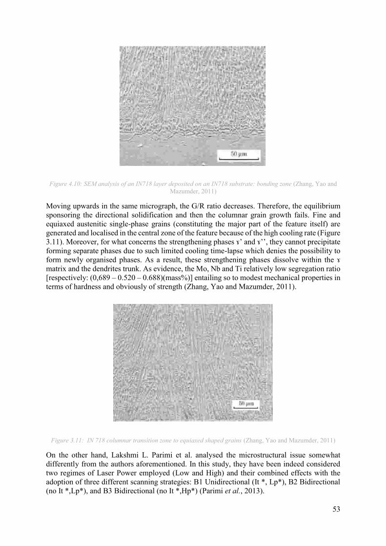
53
Figure 4.10: SEM analysis of an IN718 layer deposited on an IN718 substrate: bonding zone (Zhang, Yao and
Mazumder, 2011)
Moving upwards in the same micrograph, the G/R ratio decreases. Therefore, the equilibrium
sponsoring the directional solidification and then the columnar grain growth fails. Fine and
equiaxed austenitic single-phase grains (constituting the major part of the feature itself) are
generated and localised in the central zone of the feature because of the high cooling rate (Figure
3.11). Moreover, for what concerns the strengthening phases ɤ’ and ɤ’’, they cannot precipitate
forming separate phases due to such limited cooling time-lapse which denies the possibility to
form newly organised phases. As a result, these strengthening phases dissolve within the ɤ
matrix and the dendrites trunk. As evidence, the Mo, Nb and Ti relatively low segregation ratio
[respectively: (0,689 – 0.520 – 0.688)(mass%)] entailing so to modest mechanical properties in
terms of hardness and obviously of strength (Zhang, Yao and Mazumder, 2011).
Figure 3.11: IN 718 columnar transition zone to equiaxed shaped grains (Zhang, Yao and Mazumder, 2011)
On the other hand, Lakshmi L. Parimi et al. analysed the microstructural issue somewhat
differently from the authors aforementioned. In this study, they have been indeed considered
two regimes of Laser Power employed (Low and High) and their combined effects with the
adoption of three different scanning strategies: B1 Unidirectional (It *, Lp*), B2 Bidirectional
(no It *,Lp*), and B3 Bidirectional (no It *,Hp*) (Parimi et al., 2013).

54
According to that what just mentioned, is therefore here directly addressed the thermal history
issue, as not only dependent on the specific component geometry or the features thickness
transitions, but rather primary related to the scan strategy (and to the exposure parameters as
well).
In B1 and B2, the grains result to grow inclined accordingly to the scanning direction of a draft
angle, respectively of 50-60⁰ and 75-85⁰ (Figure 3.12 a,b). However, because of the different
choice of scan strategy, the results remarkably defer in terms of grains orientation. The
bidirectional deposition in B2 entails to grains growth towards opposite directions and
intersecting each other at 90⁰ -100⁰ when two different layers are overlapped. On the other
hand, in B1, the grains tend to grow slightly bent towards the deposition direction, although it
is not recognisable a continuous growth of grains belonging to different layers. Also, another
essential feature to be highlighted is the interposition of a “fine grain band” between two
successive deposited layers with the B1 approach. This particular feature is due to the low laser
power adopted then not sufficiently effective to re-melt the overlaying grains and joint them to
that depositing (Figure 3.12d). Otherwise, an epitaxial grain growth, coherent throughout the
layers, is detectable in the samples B3 where columnar grains 2-3 mm long develop at 50⁰ -
60⁰ (Figure 3.12c) (Parimi et al., 2013).
Figure 3.12: SEM micrographs of multiple layers deposition accordingly to different scan strategy and exposure parameters values: a) B1 Unidirectional deposition with Lp*, b) B2 Bidirectional deposition with Lp*, c) B3 Bidirectional deposition with
Hp* and d) Detail of the Fine-grain zone present in a (Parimi et al., 2013).
It *: Idle time of around 6s deriving from the laser source switch off as the current track is deposited and the time required to displace the
deposition head at the track start. During the deposition head motion, the powder stream is kept fluxing so that to force more the previous
track cooling. Lp: (Low Laser Power) 390W of laser power employed in conjunction with a laser scan speed of 200 mm/min and a powder flow rate of 18
g/min.
Hp: (High Laser power) 910W of laser power employed in conjunction with a laser scan speed of 200 mm/min and a powder flow rate of 18
g/min.

55
Thanks to an EBSD analysis, Lakshmi L. Parimi et al. deeply investigated the three builds
texture. Taking into consideration a more substantial zone of study is possible to address the
microstructural continuity issue directly. As aforementioned, in B1, a fine-grains band
generated interposing between two successive layers is evident. More explanations related to
this feature are provided in Figure 3.13a, where, in the B1 EBSD micrograph are recognisable
alternating bands constituted by fine-grains structure randomly distributed. Furthermore,
moving towards the build top, the band thickness considerably decreases because of the higher
heat storage as a consequence of a lower and lower substrate chilling effect. Although the B2
sample is characterised by higher temperatures involved during the deposition as previously
detailed, the same band is present between the alternating oriented layers, albeit with a more
modest thickness and smaller grains size (Figure 3.13b). The fine-grain band is indeed caused
by the high thermal conductivity of the IN718. Otherwise, in B3, no parting bands are
detectable. In fact, the fine equiaxed grains generated at each layer Melt Pool top, are re-melted
and they take part of the epitaxially growing grains leading to a continuous columnar structure
parallel to (001) direction (as FCC), interrupted only when the last layer is deposited in short
and independent columnar grains because of the high cooling rate promoted by the deposition
atmosphere and by the meagre heat storage in the just below surface zone (Figure 3.13c) (Parimi
et al., 2013).
Figure 3.13: EBDS micrograph and texture a) B1, b) B2, c) B3 (Parimi et al., 2013).

56
3.3.2 SEM / EBSD: Phases and chemical composition in “as-deposited conditions.”
The SEM analysis of the specimens, B1 and B2 reveals a heterogeneous microstructure in terms
of phases present. In the inter-dendritic zones, irregular, circular and squared features are
detected. These, thanks to an EDS analysis coupling, are then found as Laves phases and
Carbides.
The formers are typically rich in Nb, Mo and Ti and mainly formed because of the Nb
segregation leading to a composite interaction with other elements such as Ni, Cr and Fe. More
precisely, the laves phase composition and stoichiometry are (Ni, Fe, Cr)2(Mo, Nb, Ti) instead
of that of ɤ’’ which is (Ni3Nb). Because of the Laves’ detrimental effect on the mechanical
properties, is generally performed a solution heat treatment to dissolve them within the matrix.
Furthermore, it has been found a sort of correlation between the laser power employed and the
laves particles size. According to that, more massive particles in size range of 20-30µm and
around 100µm long, are found at high laser power (as for B3) hence, entailing a higher part
cracking risk when in operation (Parimi et al., 2013).
For what concerns the precipitates found ranging in size between 200-300nm and rich in Mo
and Nb, it is reasonable to assume that are carbides. Nevertheless, as reported in Figure 3.14,
finer carbides can be included within laves phases, whereas the coarser ones can be dispersed
in the ɤ matrix (Parimi et al., 2013).
Furthermore, observing Figure 3.15, it results clear how manifold phases generated from the
elements mentioned above segregation, coexist in the same area. At high Laser Power employed
as for B3, is not unusual to detect nearby laves phases (besides carbides), δ-phases needles
shaped. Even though usually the δ-phases are generated by high temperatures applied for a
relevant time-lapse (100h at 750-1000 ⁰ C), they can anyhow rise in such fast and dynamic
process, because of the large amount of heat stored during the deposition between the layers.
Nevertheless, the δ-phase precipitation is sponsored by the stacking-faults sites that lower the
minimum temperature necessary to make them nucleate. The reason why these phases are so
monitored and undesired is due to their relevant brittleness that in conjunction with their
acicular shape act as optimal crack initiators candidates.
On the other hand, it is also somewhat relevant to mention their strengthening effect at the grain
boundary when the material in operation is subjected to creep conditions. However, the reader
is reminded to consider that, as for the Laves and the ɤ’ / ɤ’’ phases, the thermal cycling induced
by the successive deposition, generally does not cause relevant further coarsening of δ-phases
as well. Assuming the thermal layer history previously reported in Figures 3.6 and 3.7, and
considering that the δ-phase precipitation lapse it ranges between 750-1000 ⁰ C with a
maximum at 900 ⁰ C, the temperatures in play and the time lapses dedicated to the precipitation,
seem to be inefficient (Parimi et al., 2013).
Also, it could be noteworthy, to analyse the same issue from an opposite perspective according
to which, wanting to minimise the percentage of detrimental phases as the just listed are, an
effective measure to adopt is to increase the cooling rate by appropriate process parameters set.
To conclude, it can be said that at the parity of scan speed and feed rate as well, higher Laser
Power entails to a remarkably homogeneous and columnar microstructure. This microstructure
is moreover deemed stronger than that achievable at lower Lp, even though detrimental phases
such as Laves and δ-phases or carbides as well, are present. Commonly δ-phases are not
included in samples built at modest Lp; however, they exhibit a heterogeneous microstructure
indeed composed by columnar grains mixed to equiaxed ones, that in the overall show lower
mechanical properties respect to that exhibited by samples B3 like (Parimi et al., 2013).

57
Figure 3.14: SEM micrographs reporting the Laves, Carbides and ɤ’ phases in a B2 sample like (Parimi et al.,
2013)
Figure 3.15: SEM micrographs reporting the Laves, Carbides and δ-phases in a B3 sample like (Parimi et al., 2013).

58
Finally, in Table 7 are reported the EDS scan results in terms of different chemical elements
percentage which has been detected in different areas of the B2 sample. These have been then
pertinently indexed concerning the specific phase that they may represent (Parimi et al., 2013).
At this purpose, to index the features depending on their chemical composition detected by
EDS, it results of primary importance to analyse the Nb content. This parameter can be indeed
assumed as threshold factor on which distinguishing the different phases. Table 5 provides some
Nb content ranges to be intended as a general benchmark, whereas Table 6 details the alloying
elements present about the different carbides types detectable in Ni superalloys.
Table 5: Typical Nb content of the phases present in the Ni superalloys
Phase Nb content range
(%)
ɤ Matrix ~ 4*
Carbides ~10 (also rich in Ti)
Laves >17
δ phase ~5-8
*Note: During the EDS detection it can happen to record Nb values sensitively lower than the 4%. In this case, one of the
most probable explanation is a depletion of Nb from the matrix, times to create Laves, carbides or δ-phases as well, in the
neighbouring areas.
Table 6: Typical Ni superalloy carbides types and their alloying elements markers (Minet et al., 2019).
Carbide type
Typical alloying elements
MC W, Ta, Ti, Mo, Nb, Hf
M7C3 Cr
M23C6 Cr, Mo, W
M6C Mo, W, Nb

59
Table 7: EDS compositional results provided by Lakshmi L. Parimi et al., indexed with the phases they represent
(Parimi et al., 2013)

60

61
4. Materials and Methods
In this experimental campaign, have been analysed three different types of features: 40
“Single Scan Tracks” (SSTs), 24 “Single Layers” (SLs) and 3 “Cubes”. Indeed, the laser-
related parameters like laser power (P) and laser scan speed (SS) were selected according
to the SSTs analysis, whereas the optimum hatching distance (Hd) was estimated according
to the SLs. Nevertheless, the Cubes (realised with the optimal parameters chosen P 600W,
F 750 mm/min and Hd 0.3 mm) have been analysed in their microstructural morphology,
defectology presence and phases.
In this section are briefly detailed the operative procedures adopted in order to prepare the
specimens for the different characterisation tests.
Furthermore, the equipment employed will be briefly introduced in conjunction with the
tools and the expandable materials used such as polishing cards and pads, chemical etchant
and lubricants.
4.1 Feedstock particles
The feedstock used to realise the features characterised in this campaign is constituted by
gas atomised particles sphere-shaped with a coarse average size ranging between 44 and
106 µm.
Table 7, thanks to the courtesy of 4DHybrid group, reports the particles chemical
composition investigated by EDS. The same result to be rich in Ni, Cr, Fe and Nb aside
from with a not negligible Ti and Al presence.
Further specifications about the feedstock particles morphology and hallmarks will be
morevoer detailed in paragraph 4.3.1.3 pertinently to their influence on the deposition
performances.
Figure 4.1: SEM Powder particles analysis

62
Table 7: Powder particles’ feedstock chemical composition
4.2 DED Machine
Figure 4.2: Laserdyne 430 - DED Machine (Laserdyne 430 | Primapower, no date).
Machine specifications (Laserdyne 430 | Primapower, no date)
Work area
3-4 axes:
X 585 mm, Y 400 mm, Z 500 mm, Rotary 360° (optional)
5-6 axes:
X 585 mm, Y 400 mm, Z 500 mm, C 900°, D 300°, Rotary 360° (optional)
Axis speed
3-4 axes:
X, Y, Z: 15 m/min; Rotary: various options
5-6 axes:
X, Y, Z: 15 m/min; C, D: 90 rpm; Rotary: various options
Accuracy
3-4 axes:
X,Y,Z: 12.5 µm; Rotary: various options
5-6 axes
X,Y,Z: 12.5 µm; C, D: +/- 6 arc-sec; Rotary: various options
Laser source: CW, QCW, pulsed fibre laser
Element Atomic concentration Weight concentration
Nickel 52.67±0.53 55.79±1.91
Chromium 18.76±0.77 17.67±0.20
Iron 19.04±1.59 16.15±0.29
Niobium 3.42±0.86 6.67±0.22
Molybdenum 2.09±0.05 3.88±0.11
Titanium 1.05±0.24 1.10±0.10
Aluminum 1.28±0.16 0.64±0.13

63
4.3 Stereomicroscope
The “On top” characterisation dedicated to observing the external surface of the features in question, it has been run employing a LEICA EZ4W Stereomicroscope. More specifically, thanks to this equipment it has been possible observing the SSTs from the top, at the two magnification of 10X and 12,5X, to evaluate their regularity and homogeneity of deposition.
Figure 4.3: LEICA EZ4W Stereomicroscope
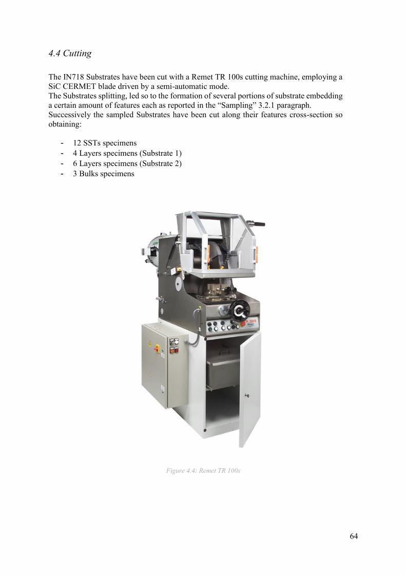
64
4.4 Cutting
The IN718 Substrates have been cut with a Remet TR 100s cutting machine, employing a
SiC CERMET blade driven by a semi-automatic mode.
The Substrates splitting, led so to the formation of several portions of substrate embedding
a certain amount of features each as reported in the “Sampling” 3.2.1 paragraph.
Successively the sampled Substrates have been cut along their features cross-section so
obtaining:
- 12 SSTs specimens
- 4 Layers specimens (Substrate 1)
- 6 Layers specimens (Substrate 2)
- 3 Bulks specimens
Figure 4.4: Remet TR 100s

65
4.4.1 Sampling
Figure 4.5: SSTs Substrate 1 - Sampling
Figure 4.6: Layers Substrate 1 - Sampling

66
Figure 4.7: Layers Substrate 2 – Sampling
Figure 4.8: Bulks 4, 5 and 6 - Sampling

67
4.5 Mounting
After the cutting operations, the twelve SSTs samples have been then embedded in
epoxydic resin made curing within plastic moulds for around 30 minutes Figure 65.
This procedure resulted indeed necessary in order to make more accessible and more
accurate the further polishing procedures so enabling to keep the cross-section surface
parallel to the rotating card/pad. Thanks to a larger area in contact with the abrasive unit,
it has been possible to ensure a more robust and reliable coupling between the two corps
constituting the tribosystem limiting the samples oscillation and their good grabbing from
the operator.
Figure 4.9: Plastic mould containing a curing epoxydic resin embedding the SSTs specimens
Otherwise from the SSTs, the Layers and the Bulks samples have been not “mounted” as just
discussed above, since owning to enough adjunctive areas surrounding the feature’s cross-
section, ensuring a compliant handleability of the sample in polishing.

68
4.6 Polishing
The polishing operations have been run employing a Presi Mecatech 234 polishing
machine reaching a final Ra value of around 1 µm.
More in detail, this target roughness has been reached employing a set of abrasive cards
respectively of #FEPA:
- 300
- 600
- 800
- 1200
- 2000
- 2400
Moreover, two pads bearing a mixture of diamond particles of 3 and 1 µm in an average
size and a lubricant solution alcohol-based.
Figure 4.10: Presi Mecatech 234
More precisely, the samples have been polished changing their orientation at ± 90⁰
(respect to the polishing tangential direction) each time a different abrasive power
polishing card has been changed. This shrewdness allowed indeed to attach the samples’s
superficial peaks more effectively.
Otherwise, the samples have been rotated from the same angle range aforementioned while
they have been polished with the pads at 3 and 1 µm in order to achieve a more isotropic
and homogeneous surface.

69
Finally, between each polishing step, the surface of the sample has been cleaned with soap
and water with the intent to remove eventual debris or residual diamond particles as well,
still leaning on the surface.
Moreover, as adjunctive cleaning step, the samples have been drowned in a backer
containing ethanol absolute and placed in an ultrasonic bath for around 3-5 minutes.
In Figure 67 are reported the SSTs cross-sections as polished at 1 µm observed with a
LEICA DMI 5000 optical microscope at 50X.
Figure 4.11: SSTs cross-section polished at 1 µm - Optical microscope
4.7 Chemical etching
After the samples surface check regarding the absence of superficial scratches due to the
eventual non-compliant polishing, the same has been chemically etched with the
metallographic etchant Kalling’s No.2 whose composition is reported as it follows:
- CuCl2 10 gr
- Hydrochloric acid 200 ml
- Ethanol absolute 200 ml
More specifically the samples have been drowned for around 15-17 seconds in the
Kalling’s No.2 solution and quenched in distilled water before being cleaned with soap
and water and then dried with compressed airflow.
Furthermore, in order to remove eventual undesired halos as a consequence of a not
optimal etching, the samples have been successfully cleaned with ethanol absolute before
their observation at the Optical microscope.

70
4.8 Optical Microscope
Employing a LEICA DMI 5000 the SSTs, the Layers and the Cubes’ cross-sections, have
been analysed respectively in their etched and as polished surfaces at 50X and 100X.
Figure 4.12: LEICA DMI 5000 Optical Microscope.
4.9 SEM
Thanks to the SEM equipment “Phenom XL” endowed of an RX detector, it has been possible
analysing the Cubes cross-sections observing the microstructure as well as detecting the phases
present through a surface compositional analysis.
Figure 4.13: SEM equipment "Phenom XL."
71
5. Results and Discussion
5.1 Purposes
The intent of this experimental campaign is to identify the optimal process parameters
dedicated to perform manufacturing and remanufacturing operations of IN718 components
by DED.
Pursuing this goal, some basics features have been at first deposited on IN718 substrates
which can also be intended as the bulk material of the component to be repaired. The
features in object (detailed as follows), have been realized by “SUPSI” on respectively
three different IN718 alloy, using not preheated substrates.
Features analyzed in “as-deposited” conditions:
- 40 IN718 Single Scan Tracks (SSTs) with no repetition.
- 20 Single Layers (SLs) with no repetition in their deposition parameters.
- Three Cubes (Blks or Cbs) built with the best process parameters.
Successively, the samples (as reported in Chapter 3) have been prepared for the
characterization process, on which the several features have been analyzed from different
perspectives aiming to verify their coherence with the substrate and their compliancy with
functional applications.
5.1.1 Features specifications and themes of analysis
The SSTs have been realized employing:
8 Feed rate levels, F [mm/min]: 300, 450, 600, 750, 900, 1050, 1200, 1350
5 Laser Power levels, P [W]: 300, 400, 500, 600, 700
and characterized in:
Tracks morphology and regularity
Heat Affected Zone (HAZ) width
Melt Pool morphology and regularity after etching
Coherence with the substrate
Having collected and critically assessed the results obtained, some specific sets of process
parameters have been recognized as appointed to generally provide an optimal deposition*.
Successively, having identified the best process areas, the deposition compliancy issue has
been then reported to a larger scale analyzing different depositions of Layers and Cubes.
*At this purpose, it must be noted that the results successively reported have not the intention to validate a
depositional compliancy relatively to all the applicative cases. In fact, as mentioned in Chapter 2, the part
thermal history it is not only related to the process parameters set but rather, to a vaster number of variables
as for instance the part’s shape, the powder chemical composition and the process environment.
The SLs of Substrate 1 have been realized employing:
A unique Laser Power level, P [W]: 600
2 Feed rate levels, F [mm/min]: 750, 900
2 Hatching distance, H [mm]: 0,3, 0,4
and that of the Substrate 2 adopting:
A unique Laser Power level, P [W]: 400

72
2 Feed rate levels, F [mm/min]: 750, 900
2 Hatching distance, H [mm]: 0,3, 0,4.
Furthermore, the SLs of both substrates have been characterized in:
Regularity
Porosity/Oxides percentage area
Etched morphology
The 3D Bulks analyzed have been realized employing:
A unique Laser Power level, P [W]: 750
A unique Feed rate level, F [mm/min]: 900
A unique Hatching distance H [mm]: 0,3
Layer thickness dz [mm]: 0,2
Hatching Raster strategy: 0⁰ /90⁰ /45⁰ /135⁰ /60⁰ /120⁰
and characterized in:
Porosity/Oxides percentage area
Microstructure
Laves phases percentage area
Finally, an overview of the results obtained has been reported pertinently to some summary
maps and a process software simulation of a simple feature has been attempt.

73
5.2 Single Scan Tracks characterization
Figure 5.1: SSTs-Substrate 1
Table 8: Exposure parameters and SSTs indexing.
5.2.1 Single Scan Tracks morphology
To analyze the as-deposited SSTs morphology, an “On Top” inspection at a magnification of
10X has been performed by a LEICA EZ4W stereomicroscope.
Focusing the SSTs at 10X, it has been possible to consider enough large shot of the features
considered, which enclosed all the relevant hallmarks and the eventual deposition defects on
which base the further morphology compliance evaluations.
FEED RATE [mm/min]
LASER
POWER
[W]
300 450 600 750 900 1050 1200 1350
300 9 10 11 12 13 14 15 16
400 25 26 27 28 29 30 31 32
500 17 18 19 20 21 22 23 24
600 1 2 3 4 5 6 7 8
700 33 34 35 36 37 38 39 40

74
Each featured image has been then collected in Figure 5.2 pertinently to the process parameters
employed with which they have been realized and classified accordingly a stable or not stable
deposition. This first distinction had the intent to distinguish eventual uncompliant tracks which
presented unacceptable defectology of deposition, such as lacks of deposition, therefore
considered as evidence of not reliable process parameters set.
Figure 5.2 SSTs “On top” analysis: red outline whether homogeneous deposition, red outline whether
inhomogeneous deposition and blue outline labelling process instabilities

75
More in detail, all the SSTs depositions have been deemed stable except for the SSTs 21 (P
500W and F 900 mm/min) and 25 (P 400W and F 300 mm/min) as highlighted in Figure 5.2
(blue outline).
However, it is necessary to specify that no evaluations about the depositions repeatability can
be provided pertinently to this campaign since the same have been uniquely realized. Therefore,
the possibility to obtain compliant results at the same process parameters, cannot be neglected
in further evaluations.
The defectology detected in SST 21 (Figure 5.3) could be likely caused by an equipment
instability (like a sudden deposition head acceleration) or by a shutter time in which the
deposition head has been not properly fed. However, to properly validate this theory, it would
be suggestable to repeat the deposition for a larger number of times properly setting the
equipment, so verifying whether the defectology occurs again or not.
Figure 5.3: Process instability - SST n⁰ 21.
Another defectology representative of an unstable deposition has also been detected in SST 25
(Figure 5.4). Likely due to the modest transverse speed and the low laser power level employed,
it can be assumed that in this instance the resulting specific energy was not high enough to
accomplish a right material melting (see section 1.1.5.2.1.2). As a result, the deposition obtained
exhibits an evident discontinuity in its middle with an apparent lack of material. Since the
energy source used resulted to be insufficient to homogeneously melt the mass of the particle
fluxed, the track’s profile moreover consistently deviates from a straight path, thus suggesting
a not uniform/stable dynamic melt pool generation during the deposition.
Finally, it can be added that the rounded protuberances observable on the SST’s profiles, could
be likely due to a week wettability of the melt pools which cannot properly joint together
creating smooth edges because of the values of the parameters set.

76
Figure 5.4: Process instability - SST 25.
Furthermore, the present analysis has been deepened (excluding the two just analyzed tracks)
evaluating the SSTs deposition profile regularity or irregularity, considering the eventual
linearity deviation of the edges.
According to that, each SST has been assessed in its morphology appearance and labelled with
either a green or a red outline, whether the deposition was considered compliant or not-
compliant accordingly an obvious criterion of homogeneity Figure 5.2.
The outcomes obtained, revealed that setting the equipment at low scan speed F and medium-
high laser power P, the interaction between the deposited material and the substrate is
remarkably severe. Therefore, this phenomenon entails an inhomogeneous deposition besides
a pronounced HAZ. This latter feature will be successively analyzed separately.
Specifically, three SSTs (four considering also the not stable 25th deposition) out of five
deposited at scan speed of 300 mm/min and at laser power of 500W, 600W and 700W
respectively, resulted to be not-regular. In addition, also the SSTs 2 (450mm/min, 600W), 3
(600mm/min, 600W), 34 (450mm/min, 700W) and 35 (600mm/min, 700W) resulted not
compliant Figure 5.2. As a result, a not compliancy process zone has been detected, therefore
the coupling of the respective process parameters creating it have been deemed as not optimal
to perform reliable repairing features.
5.2.2 SSTs and Heat Affected Zone (HAZ) regularity
The first analysis run wanting to deepen the interaction between the as-deposited material and
the substrate; took into consideration the Heat Affected Zone as appeared on the substrate
surface. Because of its importance in terms of supply material adhesion and coherency with the
substrate, this parameter has been so considered as a key feature on which furtherly assess the
tracks compliancy. Therefore, so that were possible to measure the HAZ width, further images
of the SSTs, considering have been acquired at a magnification of 12,5X. More in detail,
considering a precautionary approach, for each feature have been considered the images which
included the larger number of defects and irregularities. The HAZ width has been then sampled
and measured, by means of the software “ImageJ”, five times at the two magnification of 10X
and 12,5X for a total amount of ten measurements for each SST. With the data obtained
(reported in table 9), they have been calculated the Arithmetic Mean “A” and the Standard

77
Deviation “SD”, then plotted in their trends pertinently to the laser power and Feed rate levels
from which they derived (Figure 5.5).
Table 9: HAZ “A” and “SD” values at different Laser Power and Feed Rate levels.
Figure 5.5- Figure 63 (shadowed): HAZ Arithmetic Mean “A” and Standard deviation “SD” as a function of
Laser Power and Feed rate levels – representative SST in which the HAZ Width has been displayed.
Laser Power
vs Feed Rate
Laser Power P [W]
300 400 500 600 700
Feed Rate F [mm/min]
A [μm]
SD A
[μm] SD
A [μm]
SD A
[μm] SD
A [μm]
SD
300 216 16.9 303.5 40 433.1 39 353.5 33.8 628.4 104
450 218.5 43.9 221.8 57.9 341 80 279.8 19.4 459.5 55.7
600 200 21.2 236.6 39.1 253.3 50 326.6 32.5 246.2 50.2
750 138.6 17.3 163.3 27.3 180 41.9 308.2 25.6 310.2 40.3
900 117.8 28.5 218.2 56.2 194.2 62.9 244 40.8 335.7 67.8
1050 98.8 28.9 192.7 36.5 141.3 28.2 210.9 27.8 251.2 28.4
1200 76.4 8.6 95.4 23.8 144 30.4 197.2 33.4 201.5 28.8
1350 56.4 16.4 76.4 25.4 149.8 42.3 199.5 28.2 169.5 36.2

78
In the overall, the HAZ Arithmetic Mean width decreases at parity of laser power level as the
feed rate and the scan speed increase. This phenomenon finds moreover confirmation in the
literature, according to which increasing the scan velocity at parity of laser power value, the
specific energy provided to the substrate on unit of area, decreases (see section 2.6.2.2.2,
Equation 2.1). Therefore, in the case in point the interaction with the substrate is less severe
and then the interface thickness in which the two phases institute an equilibrium boundary.
However, in Figure 5.3 can be noticed some incongruences with this theory. In particular the
SSTs “28” (P 400 W, F 750 mm/min), “20” (P 500 W, F 750 mm/min), “2” (P 600 W, F 450
mm/min) and “35” (P 700 W, F 600 mm/min) shown HAZ widths respectively higher than that
of the SSTs deposited at the same P level but at a lower F value. Furthermore, each “A” value
bar, has been coupled with an error bar representing the respective SST’s Standard deviation.
Unlikely from the Arithmetic Mean, it has been not possible to highlight a common trend for
the SD values. In fact, the SD floatability seems to be unpredictable since, is moreover directly
susceptible to defectology (lack of fusions, balling and so on) which locally alter the HAZ
width, aside from a great variety of process parameters and eventual setbacks of equipment
instability. According to the results just reported, the HAZ Standard deviation has been
considered an essential parameter on which base the HAZ and hence the deposition regularity
assessment.
However, was not possible to establish a threshold value on which base a compliancy
assessment by exclusion. Therefore, from the data collected was only possible to recognize the
general dependency of the HAZ’s width values with the laser power and the feed rate levels.
More precisely, it was possible to find that a direct relationship between the laser power increase
and the HAZ’s width rising exists. Furthermore, it was possible to state that the HAZ’s width
decreases with the scan speed and the feed rates increment.
5.2.3 SSTs etched Melt Pools HAZ
Referring to the HAZ width discussion just started in the previous paragraph, it can be said that
in order to assess to which extent the HAZ width can affect the SSTs deposition compliancy a
cross sectional analysis results to be fundamental.
In fact, it was not possible to find in literature a specific values range which indicated a
threshold distinguishing compliant or not deposition. Rather, the HAZ evaluations as in
accordance with LI,Y et al., are generally made in relation to the liquid cracking phenomenon
and to the hardness variation since the substrate, throughout the HAZ, to the deposition itself
(Li, Chen and Tamura, 2018). Therefore, in order to verify the eventual liquid cracking
occurring, the single SSTs have been etched and observed in their cross sections by means of
an optical microscope at a magnification of 100X. From the analysis run, no presence of cracks
within the Melt Pools has been detected, also in correspondence of the SSTs which exhibited
the most pronounced HAZ. However, even though no liquid cracking phenomena have been
detected (also at the most pronounced HAZs), it has been recognized that a too large interaction
with the substrate in this sense, must be avoided. In fact, large HAZ widths values mean high
areas overlaying the depositing layer metallurgically altered. As a consequence, bringing these
considerations to a macroscale perspective, because of the layering approach, parts built with
process parameters responsible of a pronounced HAZ show a remarkable microstructural
inhomogeneity because of the repeated layers annealing. Moreover, the homogeneity and
continuity issues take fundamental importance dealing with repairing operations where the
substrate cannot be considered as expendable material since it is part of the functional

79
component. According to these considerations, an effective way with which quantify the HAZ
width effect could be run hardness tests in order to verify the hardness variation between the
substrate, the HAZ and the part. However, this last topic of analysis was not considered in this
assignment.
5.2.4 SSTs etched Melt Pools Morphology
Similarly to the criterion employed in the morphologic Top view analysis, assessing the Melt
Pools morphology, has been adopted a symmetry criterion.
This geometrical aspect, in its simplicity at first defines the effectiveness of the process
parameters employed and whether deposition results uniformly coherent with the substrate
along its dimensions. Otherwise, a lack of Melt Pool symmetry can prejudice the coherence
leading to interposed porosities and lack of fusion between the further overlapped (and
juxtaposed) tracks.
Therefore, according to the assumptions just made, a remarkable morphologic incompliancy
has been detected at the low Laser Power levels 300W and 400W. Respectively, the SSTs “10”,
“11”,”12”,”13” and “26”, “27”, “28”, “29”, “30”, “31”,”32” exhibited an irregular Melt Pool
profile due to the low Specific Energy used which resulted inefficient to properly melt the
substrate in the unit of time dictated by the transverse speed.
The aforementioned SSTs have been so deemed non-compliant and outlined in red as reported
in Table 10.

80
Table 20: SSTs etched Melt Pools - 50X optical microscope

81
5.2.5 SSTs etched Melt Pools coherence with the substrate
Thanks to the different substrate and deposited material corrosion rates, it has been possible to
accurately recognize the Melt Pool’s main features: “Bead Height”, “Melt Pool Width” and
“Fusion Depth” (Figure 5.6). Therefore, the etched Melt Pools images (reported in table 11),
have been acquired at a magnitude of 50X and the features measured by the software ImageJ.
From the data collected (Table 12), it is possible to state that the “Bead Height’s” steadily
decreases as the feed rate value increases at fixed P (Figure 5.10). In addition, a remarkable
“Melt Pool’s Width” and “Fusion Depth’s” growth has been recorded when the Laser Power is
incremented at constant Feed rate (Figure 5.5 and 5.10). These three general trends, respectively
as a consequence of an upgraded transverse speed at parity of specific energy and, for both the
latter, of an increased energy supply at constant feed rate, find moreover confirmation in
literature as reported in section 2.6.2.2.1 However, so that were possible to better understand
the relationship between the three main parameters in the case in point, they have been furtherly
discussed and cross-referenced as follows.
Figure 5.6: SST "37" and its main features: Melt Pool Width, Bead Height, Fusion Depth and HAZ
5.2.5.1 Melt Pool’s Width, Fusion depth and Bead height
Generally, the melt pool’s width increases with the laser power rising (Figure 5.7), however
some deviations from this general trend have been found at the SSTs: SSTs “33” (300mm/min,
700W), “37” (900mm/min, 700W), “8” (1350mm/min, 600W) and “23” (1200mm/min, 500W).
These show a melt pool’s width respectively lower than that of the melt pools obtained adopting
the same feed rate and a lower laser power. At this purpose, in order to investigate the reason
of the just described discrepancies, the 33rd and the 1st (300mm/min, 600W) tracks have been
selected as representative example seeing their evident non-compliancy with this general
theory. The two SSTs reported in Figure 5.7, have been obtained employing the same feed rate
(300mm/min) value but different laser power respectively of 700W and 600W, respectively for
the SST 33 (on the left) and for the SST 1 (on the right). As the quotes report, the latter own a
higher melt pool’s width than the former of around 80µm (even though created with a more

82
modest P). On the other hand, the SST 33 exhibits a more pronounced Fusion Depth zone,
deeper than that of the counterpart for more than 200 µm due to a higher P adopted as expected
from the general trend reported in Figure 5.10. Nevertheless, the same melt pool’s morphologic
traits of the example presented of an unexpected low melt pool’s width in favor of a remarkably
high Fusion depth, have been also recognized in the SSTs 33, 37 and 23. This counterintuitive
observation find explanation from a thermodynamic perspective, in the heat transfer modes
rising within the Dynamic Melt Pool during the deposition. As reported in section 3.1.2, the
heat generated within the molten material is transferred to the substrate and towards the outside
world, by a conductive and a convective manner. Comparing the two phenomena relevancy, it
can be said that seeing the remarkably high molten material speed flow, the convective heat
transfer mode is definitely the prominent one. Therefore, since the heat flow states the
solidification direction hence, the 3D melt pool’s shape (section 3.1.2, 3.1.3, 3.2), it is possible
to assume that in the SST 33, the convective flow had a predominant z-axis component because
of the high P level and the modest feed rate. As a consequence of the “directional” high specific
energy used, the melt pool so resulted with a deep Fusion depth (surrounded by an evident HAZ
as mark of a too severe depositional interaction with the substrate) rose more respect to the melt
pool’s width. Nevertheless, this trend is confirmed by the experimental data reported in Figure
5.11 according to which at parity of feed rate levels the ratio between melt pool’s width and
fusion depth decreases for increased laser power values. Furthermore, the ratio just mentioned
it represents the first key parameter on which base the melt pool’s geometric homogeneity.
More in detail, at the ideal ratio “Width/Fusion depth” value of “1”, the melt pool’s geometry
results to be rounded shape with a good melt pool’s penetration within the substrate. From the
data collected it appears also clear that this benchmark valued can be pursued increasing the
laser power (Figure 5.11). However, the experimental data reported, show a not sufficient
decreasing of the aforementioned ratio (pertinently to the laser power raising) to achieve the
ideal melt pools’ shape. At this purpose, it was recognized that the balance between the feed
rate and the laser power levels employed was not optimized. As a matter of fact, the low feed
rate used entailed to a too severe laser interaction with the substrate that created deep and
acicular melt pools. More specifically, it can be said that the specific energy supplied by the
equipment, was so mainly appointed to melt the substrate, rather than the supplied material.
Otherwise, in SST 1 have been found more proportionate features dimensions respect to the
previous case. However, also in this instance a not optimized set of process parameters has
been found because of the still existing eccentricity of the melt pool. This issue is likely
imputable to a laser power slightly meagre and not able to provide the right balance between
fusion depth and melt pool’s width. To conclude, as a result of the comparisons made and from
the data displayed in Table 10, it is reasonable to think that wanting to keep the same melt
pool’s width in SST 33 pursuing a compliant and uniform deposition, it would be suggestable
to increase the feed rate value so lowering the severe laser interaction with the substrate. On the
other hand, in order to optimize the “1st” deposition at parity of F, it would be recommendable
to slightly increase the laser power up to an intermediate value between 600W and 700W.

83
Figure 5.7: Etched melt pools of the SSTs 33(on the left) and 1 (on the right) respectively indexed in their main
feature dimensions.
About the Fusion Depth analysis, a further unexpected result has been recorded. The SST 21
(900mm/min, 500W) shows at parity of feed rate a fusion depth sensitively higher than that
obtained for the 5th SST (900mm/min, 600W) even though at the same time this latter has a
larger melt pool’s width. Therefore, in this case the second trend just previously discussed
seems to be reversed suggesting a width growth at first, instead of the fusion depth, as a
consequence of the P increased. However, this particular deposition it has been intended as not
reliable at first, since the “On top” analysis revealed a remarkable defectology besides a high
HAZ SD, so witnesses of a not stable deposition.
For the avoidance of doubt, the specimens sampling has been double checked and also the SST
second half has been polished and then etched (Figure 5.8). The result has been still unvaried.
Figure 5.8: 21th SST etched Melt Pool and its not compliant Fusion Depth
About the Bead height, the measurements performed show a general increase of this feature
when the laser power rises at a constant feeding rate (Figure 5.10). Furthermore, the whether
the feed rate increases at parity of laser power the Bead height decreases. As reported in
Equation 2.2 of section 2.6.2.2.2, the Powder density is defined as the ratio between the flow
rate G (intended as mass of particles fluxed in the unit of time [g/min]) and the spot size (d)

84
times the transverse speed v. Furthermore, as reported in the experimental equation 2.4 of
section 2.6.2.2.2, the powder density directly affects the layer thickness (t) which increases or
decreases according to the powder density trend. Therefore, it can be said that in general the
layer thickness decreases according to the scan speed growth.
In Figure 5.12 is reported the “Width/Bead Height” ratio in dependence on the laser power and
the feed rate levels. More in detail, when this ratio tends to “one” the bead height results to be
perfectly balanced with the melt pool’s width exhibiting compliancy geometrical properties
appointed to obtain a good side and transversal overlapping between the tracks. However, from
the data collected in this experimental campaign it is noticeable that also at the lower scan speed
considered, the bead height shows very modest values, hence, low layer thickness. As reported
in Figure 5.12 also at the lowest scan speed value (300 mm/min), the bead height/width ratio is
about “5”, so suggesting a remarkable deviancy from the ideal value. Therefore, it was noticed
that probably the fixed feed rate value employed to supply the deposition head was to modest
for the laser power levels employed so entailing to a not compliant layer thickness and melt
pools geometry.
Finally, it can also be stated that according to the experimental data acquired in this campaign,
all the three main melt pool’s features diminish in their dimensions increasing the transverse
speed at a constant laser power.
Figure 5.9: SSTs Melt Pool width as a function of the Laser Power – red outline (process instability)
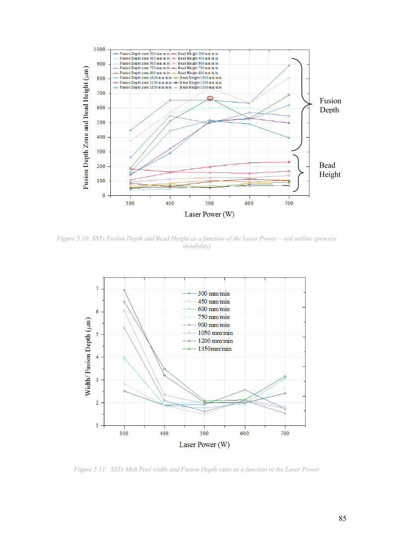
85
Figure 5.10: SSTs Fusion Depth and Bead Height as a function of the Laser Power – red outline (process
instability)
Figure 5.11: SSTs Melt Pool width and Fusion Depth ratio as a function of the Laser Power
Fusion
Depth
Bead
Height
t

86
Figure 5.12: SSTs Melt Pool width and Bead Height ratio as a function of the Laser Power.

87
Table 11: Melt Pool Width, Fusion Depth and Bead Height measurements at different Laser Power and Feed
Rate values
Laser Power [W] Feed
Rate
[mm/min]
Melt pool width [μm] Fusion Depth [μm] Bead Height
[μm]
300
300 1125 447 183
450 1065 375 108
600 1053 264 93
750 1017 261 84
900 1002 189 63
1050 981 162 54
1200 980 141 51
1350 948 147 39
400
300 1239 654 162
450 1074 570 159
600 1071 567 114
750 1054 546 63
900 1070 511 85
1050 1041 444 75
1200 1029 321 60
1350 1017 291 46
500
300 1263 656 198
450 1101 741 159
600 1068 603 123
750 1029 495 96
900 1080 666 105
1050 1017 516 56
1200 1014 504 54
1350 1068 513 69
600
300 1629 633 225
450 1359 636 153
600 1191 603 123
750 1077 570 114
900 1107 528 93
1050 1095 522 84
1200 1062 531 72
1350 1048 491 62
700
300 1545 891 231
450 1488 807 168
600 1653 537 138
750 1455 546 102
900 1062 690 108
1050 1086 621 90
1200 1206 498 69
1350 1254 396 72

88
5.2.6 SST n⁰ 37 - etched Melt Pool’s SEM/EDS analysis
Figure 5.13is reported an SEM image of the 37th SST acquired at 310x, representing the field
of analysis on which an EDS analysis has been run with the intent to identify the phases present
in the aforementioned feature.
For this purpose, in the next paragraphs the main phases detected will be listed and briefly
detailed pertinently to the results provided by the EDS analysis run, in terms of chemical
composition and XRD peaks recorded.
Figure 5.13: SST's 37 Melt Pool image acquired at 310x by SEM
(Nb/Cr based Carbide)
In Figure 5.14 is reported a Nb/Cr carbide-based, dispersed within the ɤ matrix, analyzed in its
chemical composition found by an EDS analysis as reported in Table 12.
However, referring to the alloying elements mentioned in paragraph 2.8.4 and to the carbide
types reported in Table 6, it is reasonable to think that seeing the relevant presence of Nb and
Cr, the carbide in object can be respectively related to either a MC / M6C, or to the M7C3 /
M23C6 species depending on whether the Nb or Cr local content is prominent.
Figure 5.14: Nb/Cr based carbide detected within the 37th SST Melt Pool

89
Table 12: Nb/Cr based carbide chemical composition
(Nb/Ti based Carbide)
Figure 5.15: Nb/Ti based carbide detected within the 37th SST Melt Pool

90
5.3 Layers characterization
Figure 5.16: a) Layer Substrate 1and b) Substrate 2 (on the right)
Table 13: Exposure parameters and Layers indexing.
Feed rate F (mm/min)
750 900
Laser
Power P
(W)
Hatching distance Hd (mm)
0,3 0,4 0,3 0,4
Sub 1
600
7
8
9
10
11
12
1
2
3
4
5
6
Sub 2
400
7
8
9
10
11
12
1
2
3
4
5
6
5.3.1 Substrate 2 – Inclusions
The Layers features embedded in Substrate 2 have been realised employing the same process
parameters used to deposit the SSTs 28 and 29. More in detail, the Layers 1-6 have been built
with the same P and F levels with which the SST 28 has been deposited. Also, the Layers 7-12
have been built with the same process parameters used to realise the SST 29.
Analysing the results provided in the sections 5.2.2, 5.2.3 and 5.2.4, are pertinent to the two
features just mentioned, several aspects of depositional non-compliancy can be highlighted.

91
The SST no. 28 (750mm/min, 400W) even though presents a regular deposition, seeing its
HAZ’s standard deviation lower than the 30% and its HAZ width inferior to 200µm, it reports
a remarkable melt pool asymmetry (Figures 5.17).
Figure 5.17: SST 28: regular deposition on the left and not symmetric Melt Pool on the right
Furthermore, a Melt Pool asymmetry has been detected also in the SST no. 29
(900mm/min,400W): deposition considered as non-optimal because of its HAZ width value,
and its HAZ standard deviation (Figure 5.18).
Figure 5.18: SST 29: irregular deposition on the left and not symmetric Melt Pool on the right.
However, it has been recognised in the adoption of the “modest” laser power 400W an
advantage in terms of energy consumption. Therefore, the Substrate’s two layers have been
analysed in order to verify whether a proper side overlapping of the SSTs could be obtained
despite the melt pools’ geometrical irregularity.
Therefore, with the intent to verify whether a tradeoff between the melt pools asymmetry and
an appropriate hatching distance selection would have led to a compliant deposition, it has been
run an optical analysis to assess the morphology and regularity of the etched layers as detailed
in the section 5.3.2.
Furthermore, in order to verify the feasibility of the repairing operations in relation to the
process parameters in object, the specimens obtained at two different hatching distances (of 0,3
and 0,4mm), have been optically observed in their cross-sections and analyzed pertinently to
the eventual presence of defects or inclusions as well (Table 17). Further specifications at this
purpose are provided in section 5.3.1.1 and 5.3.1.2.

92
Table 14: Substrate 2 Layers as polished at 1µm and photographed at 50X utilizing an Optical microscope.

93
In general, two types of defects can be revealed the cross-section of IN718 alloy; porosity and
oxides. However, these two different types of defects can be not quantitatively distinguished
one from each other, but instead, they can be counted as a unique feature in consequence of
optical analysis. However, it should be noticed that according to the literature, the presence of
their defects together is very detrimental for the final performance of the alloy.
Ultimately, a qualitative analysis of the oxides has been carried out in the SSTs and Cubes EDS
sections, in conjunction with their compositional specification.
5.3.1.1 Inclusions Percentage area
Each layer has been photographed around 24 times along its length and their most critical areas
in terms of residual defects, have been analysed employing the “ImageJ” software thresholding
the defects form the background considering a minimum detection size of 2 µm and a minimum
circularity of 0,5.
According to the experimental data obtained, the most relevant defect content has been detected
at the lower feed rate value of 750mm/min where the defect appears more than doubled respect

94
to that characterising the 1-6 layers. More, in particular, the higher percentage area of
inclusions/pores has been recorded for the hatching distance value of 0,3mm at F=750mm/min,
the 0,4 instead (Figure 5.19).
On the other hand, referring to the F level of 900 mm/min, this latter trend results to be reversed
since the highest area percentage has been recorded at Hd of 0,4 mm, 0,3 mm instead. The
highest A% at Hd 0,3 (repetition 1) does not overcome the lowest A% value at Hd 0,4 found in
repetition number 5 (Figure 5.19).
5.3.1.2 Inclusions Average size
For what concerns the defect’s average size, the differences observed relative to the
measurements performed on the Layers 1-6 and 7-12 cross-sections, are not substantial.
However, at F 900mm/min, it is possible to recognise a slightly higher average size respect to
that recordable in layers 7-12.
Besides, the data displayed suggest a progressive decrease in defects’ dimensions towards
successive repetitions at a constant feed rate, and the most important, towards higher hatching
distances (Figure 5.20).
Figure 5.19: Defects Percentage area as a function of the Hatching distance and Feed rate

95
Figure 5.20: Inclusions Average size as a function of the Hatching distance and the Feed rate
5.3.1.3 Inclusions discussion
According to T. DebRoy et al., three main phenomena can lead to porosity formation (Zhang
et al., 2017):
Keyhole
Gas induced porosity
Process induced porosity
However, from the optical analysis run at 50X and 100X, no Keyhole formation has been
detected. Probably due to the relatively low laser energy density levels adopted in this
campaign, none formation of irregular porosities as a consequence of the material evaporation
has been noticed.
Furthermore, analysing the single etched layers as reported in Table 16, at the boundary zone
between the melt pool and the substrate, no lack of fusions or voids have been observed as well.
On the other hand, as reported in Figure 5.17, some small circular voids spread out the layers
cross-sections can probably represent pores generated to the carrier gas entrapment.

96
Figure 5.21: Layer 7 (750mm/min, 400W, Hd of 0,3mm) cross-section – defects detected at 50X through an
optical microscope.
Also, it can be noticed that the presence of porosity found within the sample could be due to
the already existent porosity present in the feedstock powder particles. A possible pores genesis
within the part built can find the explanation in the transferred free volume from the melting
particles to the melt pool.
Therefore, this theory finds a solid base in the SEM analysis of the feedstock particles run by
4DHybrid, which reports evidence of (not yet quantified) porosity inside the gas atomised
particles (Figure 5.22).
Figure 5.22: the cross-section of the starting powder used in this work.
However, as already stated, it is not possible to quantify the porosity content with respect to
that of the oxides since the two species promiscuity and the optical inspection nature.
At this purpose, indeed, an EDS analysis would be more effective in order to precisely identify
the oxides and their composition even though the quantification uncertainty would persist.
Furthermore, it has to be also recognised that even though it was possible to quantify the
porosity percentage area, this last datum would be not so meaningful in terms of reliability.
Seeing the local nature of the cross-sectional analysis run would be not possible to verify the
results reliability relatively all the deposition dimensions.
At this purpose, would be more effective run a 3D pores distribution analysis with a
tomographic approach (analysis method not adopted in this experimental work).

97
As already introduced, the presence of oxides has been detected. Investigating the causes that
led to the formation of the oxide and embedding within the part, it has to be at first considered
the non-adoption of shielding gas during the material deposition. In fact, due to this process
choice, the environmental conditions have likely induced the formation of the oxide because of
the interaction between the oxygen present in the deposition environment and the overheated
depositing material.
Nevertheless, in the oxides’ genesis, the impurities and the oxides pre-existing within the
feedstock particles played an important role. In fact, according to the 4DHybrid EDS analysis
the particles exhibit, in conjunction with satellites and partially melted particles on their surface
(Figure 5.23), partially oxidised particles Al and O rich that can be embedded in the melt pools
during the deposition (Figure 5.24).
Figure 5.23: IN718 feedstock particles bearing satellites, partially melted particles and oxides on their surfaces
– Coarse size distribution ranging between 44 and 106 µm.
Figure 5.24: IN718 feedstock EDS analysis and chemical elements mapping
To conclude, the layers defects analysis revealed a miscellaneous presence of pores and oxides
not directly distinguishable in terms of relative quantity.

98
Also, referring to these two types of defect the most probable causes have been recognised as
deriving from equipment setbacks as carrier gas entrapment leading to circular pores or oxides
generation because of the non-adoption of shielding gas flow rate.
For both of these defects, it has been moreover detected a direct influence of the feedstock
particles composition and morphology seeing the spheres including of pores and oxides
generated during their atomization process. Furthermore, the EDS analysis of the feedstock,
suggests the presence of aluminium oxides even though further compositional details are left to
the next Cubes’ EDS analysis. The residual defects analysis showed that the level of this defect
at 750 mm/min is higher than that recorded at 900 mm/min for the modest value of 0,06%
whereas the maximum average size recorded in the first layer repetition is of 41,7 µm.
Therefore, it can be concluded that independently from the relative quantity, the defect quantity
and average size can be assessed as generally low.
5.3.2 Substrates 1 and 2 – etched layers morphology 98
Wanting to establish what set of process parameters entailed to the most homogeneous (and
compliant for repairing) deposition, the layers of the substrates 1 and 2 were compared in their
morphology.
At this purpose, the etched cross-sections (Tables 17 and 18) were optically analyzed at a
magnification of 50X and 10X, noticing at what results of coherence with the substrate and
depositional homogeneity led the respective melt pools features analyzed in section 5.2.5 (Table
15 and 16) and their morphological aspects (section 5.2.4), as a consequence of their
overlapping.
Table 15: Melt Pool's main features dimensions obtained at P 400W and respectively F of 750 and 900 mm/min.
Table 16: Melt Pool's main features dimensions obtained at P 600W and respectively F of 750 and 900 mm/min.
Analysing the best layers repetitions obtained at 400W in comparison to that obtained at 600W
at a constant feed rate and hatching distance, a substantial difference of coherence and
homogeneity has been noticed in the overall. In fact, the depositions performed at 600W, show
a better inter SSTs overlapping besides a higher fusion depth and coherence with the substrate.
In order to demonstrate the superior compliancy of the Substrate’s 1 depositions compared to
that of the Substrate 2, it has been considered as representative example the comparison
between the layers 9 (Sub. 2) and 6 (Sub. 1).
As reported in Table 14, the layer 9 of the Substrate 2 has been deposited with the lower values
of Feed rate and hatching distance considered in the layers campaign. On the other hand, the
layer 6 has been built adopting the higher scan speed and hatching distance with a 600W laser
power level.
Laser
Power
P (W)
Feed rate
F
(mm/min)
Melt Pool’s width (µm) Fusion depth (µm) Bead Height
(µm)
400
750 1054 546 63
900 1070 511 85
Laser
Power
P (W)
Feed rate
F
(mm/min)
Melt Pool’s width (µm) Fusion depth (µm) Bead Height
(µm)
600
750 1077 570 114
900 1107 528 93

99
Therefore, since an increase in feed rate generally entails a lowering of the melt pool size, it
can be said that the worst-case in terms of SSTs lateral overlapping it has been chosen referring
to Substrate 1. On the other hand, the best condition to maximise the SSTs overlapping, hence
low F and Hd, have been considered selecting the layer of comparison in Substrate 2.
As shown in Figure 5.25, even adopting a low scan speed and hatching distance, the melt pools
overlapping result to be unstable and inhomogeneous along the layer’s width. Even though the
Melt Pools seem to be acceptably overlapped side to side, their relative fusion depth varies
remarkably showing a not homogeneous coherence between the layer and the substrate.
Moreover, the micrograph revealed for the layer 6 of the substrate 1 shows a more stable and
homogeneous deposition compared to that of its counterpart considered. Regardless of a
significant hatching distance and scan speed adopted, the 6th deposition at 600W shows a very
good SSTs overlapping besides a constant fusion depth.
Figure 5.25: Micrograph of the etched layers a) 9 of the Substrate 2 and b) 6 of the Substrate 1 respectively
acquired at 50X and 100X.
Therefore, according to the assumptions just made and seeing the results discussed in section
4.2.4 relatively to the SSTs morphologic compliancy, the 600W laser power level has been
recognised to be as the optimal choice. Besides, the layers bead heights are in this case,
sensitively higher than that achieved at 400W. Therefore, adopting the 600W as the laser power
level is possible to increase the repairing rate at the expenses of lower dimensional accuracy.
Furthermore, in order to guarantee a higher deposition coherence and process stability, the
hatching distance of 0,3 and the Feed rate of 750 mm/min has been selected as preferred.
Although these latter choices entail a slight loss of process productivity, the advantages just
mentioned have been considered prominent: mostly considering the assumed purposes to which
the process is dedicated.

100
Table 17: Micrographs of the Substrate’s 2 layers etched cross sections acquired at 50X (optical microscope)

101
Table 18: Micrographs of the Substrate’s 1 layers etched cross sections acquired at 100X (optical microscope)

102
5.4 Bulks/Cubes Characterization
Figure 5.26: Unique Substrate – Bulks characterized: 4, 5 and 6
Table 19: Exposure parameters and Cubes indexing.
Feed rate F (mm/min)
750
Laser Power P (W) Hatching distance Hd (mm)
0,3
600
4
5
6
5.4.1 Defects analysis of the Cubes
Similar to the residual defect analysis in the SLs, an optical inspection concerning the Cubes
have been run at 50X of magnification.
In fact, following the assumptions made at the end of section 5.3.1.3, it has been deemed
noteworthy deepening the analysis of more large parts realised at the laser power level 600W
and feed rate level 750 mm/min.
Although the limited potentialities of this inspection method were already evident, it has been
anyway choosing to pursue this way in order to verify whether inclusions were present and to
what extent generally. Furthermore, the feature’s dimensions have also allowed verifying the
eventual presence of defects, such as lack of fusion and keyholes, on a vaster scale than that
granted from layers.
As reported in Figure 5.27 and 5.28, the maximum inclusions content and the average size
detected was respectively of around 0,04% and 14,8µm. These latter are noticeably lower than
that detected in the Substrate’s 2 layers 7,8 and 9 obtained at a constant feed rate and Hatching
distance but with a P of 400W. The reader is reminded of sections 5.3.1.1 and 5.3.1.2.
Although, it is prior stating that because of the respective different areas inspected the two
results have not the same grade of accuracy and reliability, the mismatch in values induces to

103
think that the higher Laser Power level has contributed to lower the porosity percentage and
size thanks to an enhanced Melt Pool wettability. However, in the analysis in point, this
assumption has to be intended as indicative since the porosity morphology is not distinguishable
from that of oxides.
Furthermore, also in this instance, no keyhole or lack of fusion phenomena were detected
throughout the whole Bulks’ cross-section.
Figure 5.27: Inclusions average size analysis performed at 50X by means of an optical microscope
Figure 5.28: Inclusions percentage area analysis performed at 50X by means of an optical microscope

104
Figure 5.29: Pores and oxides inspected in the middle of Bulk 4 – Micrograph acquired at 50X
5.4.2 Optical analysis of the etched Cubes
After the defects evaluations, in order to study the microstructure of the cubes, the Kalling no.2
solution was used to chemically etched the cubes.
The following optical analysis has the intent to inspect the microstructure’s morphology and
recognise the main grains growth phenomena ascribable to the DED process.
Furthermore, with this method of inspection, it was possible to observe the microstructural
transitions and anisotropy correlating them to particular areas of the three built (Figures 30, 31
and 32) such as the interface of substrate/deposited material, the build top/edges and core.
Figure 5.30: Etched Bulk 4 - Optical analysis performed at 50X

105
Figure 5.31: Etched Bulk 5 - Optical analysis performed at 50X
Figure 5.32: Etched Bulk 6 - Optical analysis performed at 50X

106
5.4.2.1 Top of the Cubes
Analysing the Cube 6 in its middle top, it is possible to notice a remarkable microstructural
transition from the core to the top. As can be seen in Figure 5.33, a large columnar grain growth
towards the top side is evident, and this grain growth stopped just some hundreds of microns
before the part's surface where the microstructure turns equiaxed. The explanation of this
microstructural transition funds its roots in the thermodynamic of solidification which, as
reported in section 3.1.1, is governed by two main factors: the ratio “G/R” and cooling rate
“GxR” where R is the solidification rate and G the temperature gradient. These two parameters
respectively define the shape and size of the microstructural feature within the solidifying part
according to the G and R local values. More in detail, when the ratio G/R increases, the
solidifying dendrites tend to be more and more directional so promoting an epitaxial grain
growth. On the contrary, as a consequence of a thermal gradient diminishing, the microstructure
equixially solidifies. Therefore, since in the part the temperature diminishes from the bottom
(where during the deposition much more heat is stored) to the top, the respective local thermal
gradient values decrease together with the G/R ratio upwards. As a result, when the G value
decreases under a specific threshold band, the microstructure starts changing its solidification
morphology creating a transition zone where columnar and equiaxed cells are partially
distinguishable at first, and then the microstructure becomes a homogeneous band of equiaxed
grains (Figure 5.34). Finally, because of the very high cooling rate peculiar of the DED
processes, ranging between 200-6000 K/s, the overall microstructure results to be very fine.
Figure 5.33: Micrograph of the etched Cube’s 6 top acquired at 50X (optical microscope)
Figure 5.34: Micrograph of the etched Cube 6 top acquired at 100X (optical microscope) - transition from columnar to
equiaxed microstructure.

107
Figure 5.35: Cube's 4 micrograph acquired at 100X (Optical microscope) - Columnar grains just under the Top
zone
Figure 5.36: Cube's 6 micrograph acquired at 100X (Optical microscope) - Columnar grains just under the Top
zone
Figure 5.37: Cube's 5 micrograph acquired at 100X (Optical microscope) - Equiaxial grains at the right corner
edge just under the Top zone.

108
5.4.2.2 Core of the Cubes
As can be seen from the following images, the cores’ microstructural analysis revealed a
prominent columnar microstructural morphology instead of equiaxial one. In fact, due to the
high heat stored from the part in these zones and because of the high thermal gradient value, it
is possible to state that the local G/R ratio was remarkably high during the solidification.
Moreover, the dendrites solidification directionality it has been not lost during the same’s
growing through the successive layers.
However, what it seems fundamental to be reported, is the remarkably high microstructural
anisotropy spread out all over the Cubes’ cross-section.
First, among all, the adoption of a “Raster” scanning strategy (0/90/45/135/60/120⁰ ) led to
sudden local variations of the microstructure’s directionality within the part. As a matter of fact,
following the EBSD assumptions made by Lakshmi L. Parimi et al. (3.3), a visible and repeated
“staircase” effect as a result of the scanning direction variations, was detected in the Cube’s 5
core (Figure 5.39). However, it is necessary to specify that it was possible to detect this
phenomenon in specific areas only. In fact, because of the numerous scanning variations
peculiar of the Raster strategy, the here reported micrographic results are different from that
obtained by the authors mentioned above.
More in detail, Lakshmi L. Parimi et al. addressed this issue referring to a unidirectional and a
bi-directional scanning strategy, then demonstrating the successive dendritic cells changing in
orientation detectable in the sectioning plane parallel to the deposition direction.
Otherwise, in the case in point, it is not possible to locate a plane where the “staircase” effect
is homogeneously present throughout a different cross-section, due to its 3D-1 distribution
manner.
In addition, the composition of the epitaxial growth phenomena because of the heat stored
within the part, the grain coarsening as a consequence of the induced thermal cycling, the grains'
trend to grow according to the maximum heat's flux direction and the formation of inter-
dendritic phases altering the lattice locally, led to an unpredictable morphology.
The reader is reminded of the sections of 3.1, 3.1.2 and 3.1.3 for further descriptions about the
phenomena just mentioned.
Figure 5.38: Micrograph acquired at 50X of Cube 5 (optical microscope) – Oxide

109
Figure 5.39: Micrograph acquired at 50X of Cube 5 (optical microscope) – Staircase effect
Figure 5.40: Micrograph acquired at 50X of Cube 6 (optical microscope) – Layering
Figure 5.41: Columnar inter-Melt Pool grain growth in Cube 6 – Micrograph acquired at 100x

110
Figure 5.42: Columnar inter-Melt Pool grain growth in Cube 6 – Micrograph acquired at 100x
5.4.2.3 Bottom of the Cubes
Taking into account that one of the purposes of this thesis is to evaluate the capability of the
DED process to be used as a method to repair the high-value metallic parts and thus, for this
reason in this section, the interface of “as-deposited” material and the substrate are analysed.
Interestingly, it is found that no liquid cracking phenomena or lack of fusion, were detected,
whereas sometimes a noticeable (even though very thin) melt pools’ penetrations of the
substrate can be easily recognised as shown in Figure 5.48. Also, considering the excellent melt
pools’ coherence with the substrate and between themselves, and a substantial lack of porosity
at the boundary zone, it can be said that from a morphological perspective a functional
coherence between the substrate and deposited material was achieved. The grains size detected
in the regions near the interface of deposited part/substrate is very fine because of the chilling
effect exerted by the base plate which contributes to institute a very high local temperature
gradient hence resulting in a high “GxR” cooling rate during solidification. Wanting to deal
with the morphology of the grains, an overall epitaxial and columnar growth were found in the
first layer as a result of the high “G/R” values. However, from few microns over the substrate,
the microstructure starts changing in its morphology because of the G/R value local decrease
which leads to an equiaxed grains growth sharing a transition zone with the columnar one.
Therefore, in order to better understanding these topological changes of microstructural features
within the part independence of their location, what it seems to be priory fundamental is to
consider the growth of the grains as a consequence of the scanning strategy in conjunction with
the dynamic melt pools’ characteristics.
Figure 5.43: Substrate and deposition boundary zone in Cube 4 – Micrograph acquired at 50x.

111
Figure 5.44: Substrate and deposition boundary zone and “staircase” effect in Cube 4 – Micrograph acquired
at 100x.
Figure 5.45: Substrate - deposition boundary zone and epitaxial columnar growth in Cube 5 – Micrograph
acquired at 50x.
Figure 5.46: Substrate - deposition boundary zone in Cube 5 – Micrograph acquired at 100x.

112
Figure 5.47: Substrate - deposition boundary zone in Cube 6 – Micrograph acquired at 50x.
Figure 5.48: Substrate - deposition boundary zone in Cube 6 and Melt Pools’ base plate penetration –
Micrograph acquired at 100x.
5.5 SEM/EDS Cubes’ analysis
As a consequence of the morphologic analysis, a more in-depth inspection of Cube 5 was
performed aiming to analyse the deposition in its microstructural phases and inclusions
presence.
At this purpose, new maps reporting images acquired at magnifications of 1000x, 2000x and
3000x respectively, have been reported in Figures 5.50, 5.51, 5.52 with the intent to report the
overall framework of the microstructural features. In fact, because of the limitations in the
magnification, the optical images were not suitable to be employed for analysing the
microstructure in detail. Furthermore, the EDS analysis allowed to finally validate the nature
of the detected phases and inclusions, and also be recognised by their chemical composition.
More, in particular, these latter will be separately discussed in the following paragraphs also in
conjunction with showing how the EDS tool has been exploited. Finally, an SEM analysis of
the substrates has been performed.

113
Figure 5.49: Cube’s 5 SEM analysis at 5000x – Laves-phases and oxides
Figure 5.50: SEM mapping of Cube 5 at 1000x.

114
Figure 5.51: SEM mapping of Cube 5 at 2000x.

115
Figure 5.52: SEM mapping of Cube 5 at 3000x.

116
5.5.1 Laves phases – EDS analysis
Figure 5.53: Laves phases EDS mapping and their chemical elements
A careful analysis of the phases mapped in their chemical composition, as reported in Figure
5.53, has been run positioning the analysis pointer in the region of interest..
Thanks to the X-Ray characteristic peaks emitted by the sample when stimulated by the electron
source, it has been so possible to analyze the chemical elements present in the datum region
quantitatively. As a result, the data displayed in Figure 5.49 provide an “Nb” content of 19,86%
in weight, representing the typical major of 17% Nb concentration which is peculiar of Laves
phases. Nevertheless, the Nb matrix depletion has been detected in the Laves phases
neighbouring areas, at confirmation of the Nb segregation in the inter-dendritic areas at the
matrix expenses..

117
5.5.2 δ-phases – EDS analysis
Since the δ-phases are usually generated in the Laves neighbouring areas, and because of their
needle shape, the Laves phases have been inspected along their edges with the intent to reveal
the presence of acicular phases. Even though the DED process generally does not allow to such
phases being generated because of the low temperature involved within the part and the high
cooling rates, it has been anyway possible to recognise the same (Paragraph 3.3.1).
At this purpose, the EDS inspection has been run according to a straight scan line with the intent
to highlight the difference in chemical composition between the matrix and the target phase, so
creating a linear chemical profile Figure 5.56.
As a result of the chemical profiles trends, an Nb peak at 12,49% in weight, therefore, included
in the δ-phase Nb composition range, has been recorded.
5.5.3 Carbides – EDS analysis
Besides the Laves and the δ-phases generation, the Nb segregation can also promote carbides
formation. In Figure 5.57, is reported an Nb based carbide analysed in its chemical composition
by EDS which revealed to be Nb and Ti-rich.
As aforementioned in the section 5.2.6, it is not possible to precisely state what exact species
of carbides the feature analysed belong with. However, referring to paragraph 2.8.4 and Table
4, it can be said that the feature analysed could be representative of three main species NbC,
Nb6C or TiC.
Figure 5.54: Laves phases detection in Cube 5 by the EDS analysis and their chemical composition.

118
Figure 5.55: EDS matrix “Nb” depletion in the dendritic core areas.

119
Figure 5.56: EDS scan line and δ-phases chemical composition.
Figure 5.57: SEM/EDS analysis of a Nb based carbide.

120
5.5.4 Oxide layer – EDS analysis
As reported in the representative Figure 5.58, the Cubes analysed to present an oxide layer not
homogeneous in its thickness along with the feature’s profile. At this purpose, the average
thickness and the standard deviation of the layered oxide, have been calculated respectively to
the Cube’s top and the side walls. More in detail, the oxide layer’s average thickness measured
at the top of the built amounted to 72 µm with a standard deviation “SD” of 11,97%. Besides,
the oxide layer’s inhomogeneity is also constituted by its irregular morphology because of the
embedding of non-melted particles within it. Furthermore, analysing the oxide layer’s thickness
at the side walls of the Cube 5, a relevant oxide layer thickness difference respect to that
detected at the top, has been detected. The average thickness measured at the side walls is of
19 µm with a standard deviation of 2,5%, hence differing of around 50 µm from that was
revealed in the Cube’s top.
Figure 5.58: Oxide layer SEM images - Cube 5
Nevertheless, the oxide layer inhomogeneity is also findable in its chemical composition. In
fact, as a consequence of the EDS analysis, two different types of oxides have been detected.
More precisely, in the following SEM images have been highlighted the spots in which the
layer has been analysed, and the chemical composition of the Al and Ti/Cr rich oxides detected.
Figure 5.59: Oxide layer average thickness at the Top of Cube 5

121
Figure 5.60: Oxide layer average thickness at the side walls of Cube 5
Figure 5.61: SEM/EDS analysis of the oxide layer- Aluminum oxide

122
Figure 5.62: SEM/EDS analysis of the oxide layer- Titanium oxide.
5.6 SEM/EDS Substrate
In order to appreciate the microstructural differences between an additively built part a casted
one instead, the Substrate has been analysed by SEM and EDS as well. The first findable
difference between the substrate’s matrix with the part’s one is the absence of dendritic
structures in the core. The low cooling rate (compared to that of AM) present in the casted part
solidification, leads to a more homogeneous and isotropic microstructure’s morphology of γ
matrix. Nevertheless, the phases detected and previously detailed in the SEM/EDS part’s
analysis (such as Laves-phases, carbides and δ-phases), have been found in the substrates as
well. However, because of the different manufacturing process characteristics, some of them
result to be different respect to that achieved in the DED built apart from a morphologic
perspective.
5.6.1 Carbides
As reported in Figure 5.63, the carbides’ composition result to be approximately the same
than that detected in the DED manufactured part with a prominent presence of Nb and Ti.
Also, in this instance, it is not possible to locally define the carbides stichometry even though
it is possible to venture the hypothesis of the species present according to the findable in
literature. For further specification, the reader is reminded of paragraph 5.5.4.

123
Figure 5.63: SEM/EDS analysis of a Nb based carbide.
5.6.2 Laves-phases
Otherwise from the Laves-phases detected within the part, the same generated in the substrate
appear remarkably different in their morphology. The substrate’s Laves does not exhibit a
preferential directionality unlikely from the Cube’s ones, which are directly influenced in their
morphology by the deposition direction and by the G/R ratio. Furthermore, the Laves presence
within the substrate is remarkably lower than that detected within the part in terms of percentage
area, so marking a relevant discontinuity in microstructural features hence mechanical
properties between the substrate and the deposited part.

124
Figure 5.64: EDS analysis of Laves phases.
5.6.3 δ-phases
Another remarkable difference between the part and the Substrate’s microstructure is the δ-
phases morphology. In fact, because of the lower cooling rate that characterises the casted parts
respect to that peculiar of the A.M., during the Substrate’s solidification the δ-phases result to
be coarser. Furthermore, the same is often detectable in the Laves neighbouring areas, in the
form of needle-shaped phases intersected. With the intent to more reliably qualify the species
of the needles shaped phases reported in Figure 5.59, an EDS scan line analysis has been run
wanting to analyse the variation of the chemical elements along a straight line.
As a consequence of the line scan analysis, the elements percentage profiles have been acquired
and analysed (Figure 5.65) in conjunction with their chemical composition. Therefore, from
Figure 5.65 it can be concluded that the two Nb peaks with an average value major than 5-8%
(12,1%) in weight concentration, are representative of the δ-phases crossing during the
beamline scanning.

125
Figure 5.65: EDS scan line analysis of δ-phases detected within the Substrate.
Figure 5.66: EDS line-scan analysis – chemical elements percentage profile along a straight line crossing two δ
-phases embedded in the substrate.

126

127
6.Conclusions
In this thesis assignment, it has been presented a characterisation campaign of three different
features (SSTs, Layers, and Cubes), realised in the Ni-based superalloy IN718 by Directed
Energy Deposition (powder fed) with the intent to identify the optimal process parameters with
which execute manufacturing and repairing operations of damaged aeronautic components.
More in detail, 40 Single Scan Tracks deposited at different Laser Power and Feed rate values
have been analysed in their morphologic appearance and microstructural features, so
identifying a first deposition compliancy window. Successively, the characterisation has been
extended to the two more massive features Layers and Cubes, analysing them in their
morphological and microstructural traits as well as in their presence of defectology. According
to the findings of this work, the following conclusions can be drawn;
6.1 SSTs
The “On top” analysis of SSTs depicted:
- that all the SSTs are regular in their profile and shape except no. 1, 2, 3, 17, 33, 34,
and 35.
- that at the SSTs 21 and 25 were present two process instability
- the 700W laser power level causes a severe interaction with the substrate leading to a
pronounced HAZ width.
The etched cross-section of the SSTs showed:
- the absence of “Key hole” phenomena
- the remarkable melt pools’ asymmetry of the SSTs:
no. 26,27,28,29,30,31 and 32 (obtained at 400W)
no. 10,11,12,13 (obtained at 300W)
no. 22
The analysis of the melt pools’ main features dimensions concerning the process
parameters employed showed:
- the diminishing of the Fusion depth, melt pool’s width and bead height for scan speed
increasing at the parity of P.
- the melt pool’s width and fusion depth increase whether the laser power P increases
at the parity of F
- the bead height, hence the layer thickness diminishes at a parity of P whether the scan
speed increases.
- a not compliant feed rate value utilized to supply the deposition head which entailed
to “Fusion Depth/Width” and “Bead Height Width” ratios, far from the ideal value of
“1” so entailing to melt pools generally not balanced in their geometry
All the non-compliancy of the SSTs has been summarised in Table 6.1
In response to the SSTs’ results analysis, the medium F values of 750,900 mm/min and
the medium P levels of 400,600W have been considered as optimal.
the best solution in terms of defects minimization is represented by the choice of
medium-high scan speed to compensate the high specific energy supplied.
the best solution in terms of melt pools’ features maximization is pursuable adopting
low scan speed and increasing the feed rate (amount of powder fluxed in the unit of
time).
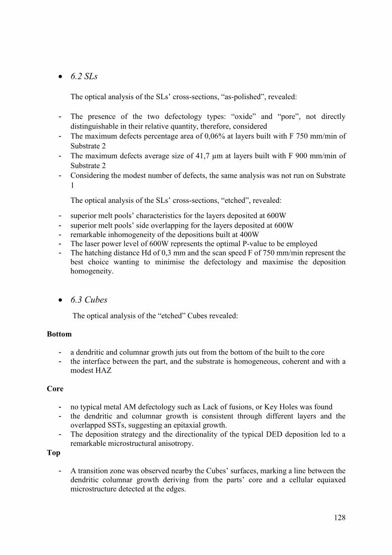
128
6.2 SLs
The optical analysis of the SLs’ cross-sections, “as-polished”, revealed:
- The presence of the two defectology types: “oxide” and “pore”, not directly
distinguishable in their relative quantity, therefore, considered
- The maximum defects percentage area of 0,06% at layers built with F 750 mm/min of
Substrate 2
- The maximum defects average size of 41,7 µm at layers built with F 900 mm/min of
Substrate 2
- Considering the modest number of defects, the same analysis was not run on Substrate
1
The optical analysis of the SLs’ cross-sections, “etched”, revealed:
- superior melt pools’ characteristics for the layers deposited at 600W
- superior melt pools’ side overlapping for the layers deposited at 600W
- remarkable inhomogeneity of the depositions built at 400W
- The laser power level of 600W represents the optimal P-value to be employed
- The hatching distance Hd of 0,3 mm and the scan speed F of 750 mm/min represent the
best choice wanting to minimise the defectology and maximise the deposition
homogeneity.
6.3 Cubes
The optical analysis of the “etched” Cubes revealed:
Bottom
- a dendritic and columnar growth juts out from the bottom of the built to the core
- the interface between the part, and the substrate is homogeneous, coherent and with a
modest HAZ
Core
- no typical metal AM defectology such as Lack of fusions, or Key Holes was found
- the dendritic and columnar growth is consistent through different layers and the
overlapped SSTs, suggesting an epitaxial growth.
- The deposition strategy and the directionality of the typical DED deposition led to a
remarkable microstructural anisotropy.
Top
- A transition zone was observed nearby the Cubes’ surfaces, marking a line between the
dendritic columnar growth deriving from the parts’ core and a cellular equiaxed
microstructure detected at the edges.

129
The SEM/EDS analysis reported:
- a remarkably high inter-dendritic Laves presence (not directly quantified
because of the optical nature of the analysis method adopted), and
- Laves presence noticed in the top neighbouring areas despite the generally low
local thermal gradient that characterises this zone
- presence of carbides Nb and Ti-rich dispersed in the γ matrix
- presence of Ti and Al oxides
- Laves phases
- Delta phases
- Ti and Al oxides dispersed in the oxide layer covering the Cubes’ surfaces
To conclude, the optimal solution in terms of process parameters employed in the
characterisation campaign considered has been identified in the adoption of P 600W, F 750
mm/min and HD 0,3 mm.

130
7. References
Akram, J. et al. (2018) ‘Understanding grain evolution in additive manufacturing through
modeling’, Additive Manufacturing. Elsevier, 21(September 2017), pp. 255–268. doi:
10.1016/j.addma.2018.03.021.
Alderliesten, R. C. (2018) ‘Introduction to Aerospace Structures and Materials’, TU Delft-EDX
online course.
Arcam EBM (2019) History - Arcam AB. Available at: http://www.arcam.com/company/about-
arcam/history/ (Accessed: 7 February 2019).
ASTM International (2019a) ASTM International - Standards Worldwide. Available at:
https://www.astm.org/ (Accessed: 7 February 2019).
ASTM International (2019b) ISO/ASTM 52900:2015(en), Additive manufacturing — General
principles — Terminology. Available at: https://www.iso.org/obp/ui/#iso:std:iso-
astm:52900:ed-1:v1:en (Accessed: 2 January 2019).
Attaran, M. (2017) ‘The rise of 3-D printing : The advantages of additive manufacturing over
traditional manufacturing’, Business Horizons. ‘Kelley School of Business, Indiana
University’, 60(5), pp. 677–688. doi: 10.1016/j.bushor.2017.05.011.
Beaman, J. J. (2001) ‘Solid Freeform Fabrication : An Historical Perspective’, SFF - Solid
Freeform Fabrication Symposium (2009), pp. 584–595. doi: 10.1007/978-1-4615-6327-3.
Bourell, D. L. D. et al. (2009) ‘A brief history of additive manufacturing and the 2009 roadmap
for additive manufacturing: looking back and looking ahead’, US-Turkey Workshop on Rapid
Technologies (RapidTech2009), (2), pp. 5–11. doi: 10.1089/3dp.2013.0002.
BRUKER (2019) Combined EBSD and EDS Analysis on SEM - Webinars | Bruker. Available
at: https://www.bruker.com/events/webinars/combined-ebsd-and-eds-analysis-on-sem.html
(Accessed: 24 May 2019).
Carlo Baese (1902) ‘Photographic process for the reproduction of plastic objects.’, US774549A
patent. Available at: https://patents.google.com/patent/US774549A/en (Accessed: 5 February
2019).
Cunningham, C. R. et al. (2018) ‘Invited review article: Strategies and processes for high
quality wire arc additive manufacturing’, Additive Manufacturing. Elsevier, 22(June), pp. 672–
686. doi: 10.1016/j.addma.2018.06.020.
Debroy, T. et al. (2018) ‘Progress in Materials Science Additive manufacturing of metallic
components – Process , structure and properties’, 92, pp. 112–224. doi:
10.1016/j.pmatsci.2017.10.001.
Digital Engineering (2019) Wohlers Report 2019: Record Growth in Additive Manufacturing
Materials - Digital Engineering 24/7. Available at:
https://www.digitalengineering247.com/article/wohlers-report-2019-record-growth-in-
additive-manufacturing-materials/design (Accessed: 30 April 2019).
European Project ‘4D Hybrid’ (2019) Objectives – 4D Hybrid. Available at:
http://4dhybrid.eu/objectives/ (Accessed: 3 February 2019).
Fayazfar, H. et al. (2018) ‘A critical review of powder-based additive manufacturing of ferrous
alloys: Process parameters, microstructure and mechanical properties’, Materials and Design.
Elsevier Ltd, 144, pp. 98–128. doi: 10.1016/j.matdes.2018.02.018.

131
Galati, M. and Iuliano, L. (2018) ‘A literature review of powder-based electron beam melting
focusing on numerical simulations’, Additive Manufacturing. Elsevier B.V., 19, pp. 1–20. doi:
10.1016/j.addma.2017.11.001.
Gasman, L. (2019) Additive aerospace considered as a business. SmarTech M, Additive
Manufacturing for the Aerospace Industry. SmarTech M. Virginia, United States: Elsevier Inc.
doi: 10.1016/B978-0-12-814062-8.00017-0.
Gibson, I., Rosen, D. and Stucker, B. (2013) ‘Standard Terminology for Additive
Manufacturing Technologies’, Rapid Manufacturing Association, pp. 10–12. doi:
10.1520/F2792-12A.2.
Gibson, I., Rosen, D. and Stucker, B. (2014) ‘Directed Energy Deposition Processes’, in
Additive Manufacturing Technologies, pp. 245–268. doi: 10.1007/978-1-4939-2113-3_10.
Goodfellow, A. J. (2018) ‘Strengthening mechanisms in polycrystalline nickel-based
superalloys’, Materials Science and Technology (United Kingdom). Taylor & Francis, 34(15),
pp. 1793–1808. doi: 10.1080/02670836.2018.1461594.
Greer, C. et al. (2019) ‘Introduction to the design rules for Metal Big Area Additive
Manufacturing’, Additive Manufacturing. Elsevier B.V., 27, pp. 159–166. doi:
10.1016/j.addma.2019.02.016.
I. Gibson, D.W. Rosen, B. S. (2010) ‘Rapid Prototyping to Direct Digital Manufacturing’,
Additive Manufacturing Technologies.
innovametric (2019) PolyWorks Modeler | InnovMetric Software. Available at:
https://www.innovmetric.com/en/products/polyworks-
modeler?gclid=Cj0KCQjw5J_mBRDVARIsAGqGLZBZcHD-
8KVmUa2USe2kiRBpkQ5xUcIuFUk0pSpytffr6CtYnKNDWCwaAgzeEALw_wcB
(Accessed: 30 April 2019).
Kumara, C. et al. (2019) ‘Microstructure modelling of laser metal powder directed energy
deposition of alloy 718’. Elsevier, 25(November 2018), pp. 357–364. doi:
10.1016/j.addma.2018.11.024.
L. Xue, M. U. I. (2006) ‘Laser consolidation-a novel one-step manufacturing process for
making net-shape functional components Processing’, Cost Effective Manufacture via Net-
Shape, (Neuilly-sur-Seine, France.).
Laserdyne 430 | Primapower (no date). Available at:
https://www.primapower.com/us/laserdyne-430/#1448982719858-0eaae0f8-b51dfc72-
a00fae4f-fbacb154-86055a6d-1b9e (Accessed: 8 July 2019).
Li, Y., Chen, K. and Tamura, N. (2018) ‘Mechanism of heat affected zone cracking in Ni-based
superalloy DZ125L fabricated by laser 3D printing technique’, Materials and Design. Elsevier
Ltd, 150, pp. 171–181. doi: 10.1016/j.matdes.2018.04.032.
Liu, R. et al. (2016) Aerospace applications of laser additive manufacturing, Laser Additive
Manufacturing: Materials, Design, Technologies, and Applications. Elsevier Ltd. doi:
10.1016/B978-0-08-100433-3.00013-0.
Mahamood, R. M. and Akinlabi, E. T. (2018) ‘Effect of Powder Flow Rate on Surface Finish
in Laser Additive Manufacturing Process’, IOP Conference Series: Materials Science and
Engineering, 391(1). doi: 10.1088/1757-899X/391/1/012005.
Mazumder, J. (2017) ‘Laser-aided direct metal deposition of metals and alloys’, in Laser
Additive Manufacturing. Elsevier, pp. 21–53. doi: 10.1016/B978-0-08-100433-3.00001-4.

132
McKinsey&Company (2018) Ops 4.0: The Human Factor--Recognizing the capability
challenge | McKinsey & Company. Available at: https://www.mckinsey.com/business-
functions/operations/our-insights/operations-blog/ops-40-the-human-factor-recognizing-the-
capability-challenge (Accessed: 3 January 2019).
MIchael Ashby, Hugh Shercliff, D. C. (2009) Materiali-Dalla scienza alla progettazione
ingegneristica.
Minet, K. et al. (2019) 8. Superalloys, powders, process monitoring in additive manufacturing,
Additive Manufacturing for the Aerospace Industry. Elsevier Inc. doi: 10.1016/B978-0-12-
814062-8.00009-1.
Molitch-Hou, M. (2018) ‘Overview of additive manufacturing process’, Additive
Manufacturing. Butterworth-Heinemann, pp. 1–38. doi: 10.1016/B978-0-12-812155-9.00001-
3.
Najmon, J. C., Raeisi, S. and Tovar, A. (2019) Review of additive manufacturing technologies
and applications in the aerospace industry, Additive Manufacturing for the Aerospace Industry.
Elsevier Inc. doi: 10.1016/B978-0-12-814062-8.00002-9.
Ngo, T. D. et al. (2018) ‘Additive manufacturing (3D printing): A review of materials, methods,
applications and challenges’, Composites Part B: Engineering. Elsevier, 143(December 2017),
pp. 172–196. doi: 10.1016/j.compositesb.2018.02.012.
Parimi, L. L. et al. (2013) ‘Microstructural and texture development in direct laser fabricated
IN718 ☆’, Materials Characterization. The Authors, 89, pp. 102–111. doi:
10.1016/j.matchar.2013.12.012.
Pierre Alfred Leon Ciraud (1972) ‘A method and apparatus for manufacturing objects made of
any arbitrary material meltable’, DE2263777A1 Patent. Available at:
https://patents.google.com/patent/DE2263777A1/en (Accessed: 6 February 2019).
Sames, W. J. et al. (2016) ‘The metallurgy and processing science of metal additive
manufacturing’, International Materials Reviews. Taylor & Francis, 61(5), pp. 315–360. doi:
10.1080/09506608.2015.1116649.
Shamsaei, N. et al. (2015) ‘An overview of Direct Laser Deposition for additive manufacturing;
Part II: Mechanical behavior, process parameter optimization and control’, Additive
Manufacturing. Elsevier B.V., 8, pp. 12–35. doi: 10.1016/j.addma.2015.07.002.
Shim, D. S. et al. (2016) ‘Effect of layer thickness setting on deposition characteristics in direct
energy deposition (DED) process’, Optics and Laser Technology. Elsevier, 86, pp. 69–78. doi:
10.1016/j.optlastec.2016.07.001.
Sims, C. T. (1984) ‘A History of Superalloy Metallurgy for Superalloy Metallurgists’,
Superalloys 1984 (Fifth International Symposium), pp. 399–419. doi:
10.7449/1984/Superalloys_1984_399_419.
Singh, R. and Singh, S. (2017) ‘Additive Manufacturing: An Overview’, Reference Module in
Materials Science and Materials Engineering, pp. 1–12. doi: 10.1016/B978-0-12-803581-
8.04165-5.
Swainson, W. K. (1971) ‘Method, medium and apparatus for producing three-dimensional
figure product’, US4041476A. Available at: https://patents.google.com/patent/US4041476A/en
(Accessed: 5 February 2019).
Tang, L. et al. (2008) ‘Variable Powder Flow Rate Control in Laser Metal Deposition
Processes’, Journal of Manufacturing Science and Engineering, 130(4), p. 041016. doi:

133
10.1115/1.2953074.
Tapia, A. S. (2006) ‘COMPUTATIONAL DESIGN OF NICKEL BASED SUPERALLOYS
FOR INDUSTRIAL GAS TURBINE COMPONENTS’, A THESIS PRESENTED TO THE
GRADUATE SCHOOL OF THE UNIVERSITY OF FLORIDA IN PARTIAL FULFILLMENT
OF THE REQUIREMENTS FOR THE DEGREE OF MASTER OF SCIENCE UNIVERSITY
OF FLORIDA.
Thompson, S. M. et al. (2015) ‘An overview of Direct Laser Deposition for additive
manufacturing; Part I: Transport phenomena, modeling and diagnostics’, Additive
Manufacturing. Elsevier B.V., 8, pp. 36–62. doi: 10.1016/j.addma.2015.07.001.
Villeneuve, F. et al. (2018) ‘Typology of geometrical defects in Electron Beam Melting’,
Procedia CIRP, 75, pp. 92–97. doi: 10.1016/j.procir.2018.04.033.
Wei, H. L. et al. (2019) ‘Three-dimensional grain growth during multi-layer printing of a
nickel- based alloy Inconel 718’. Elsevier, 25(October 2018), pp. 448–459. doi:
10.1016/j.addma.2018.11.028.
Wong, K. V and Hernandez, A. (2012) ‘A Review of Additive Manufacturing’, 2012. doi:
10.5402/2012/208760.
Wu, B. et al. (2018) ‘A review of the wire arc additive manufacturing of metals: properties,
defects and quality improvement’, Journal of Manufacturing Processes. Elsevier, 35(August),
pp. 127–139. doi: 10.1016/j.jmapro.2018.08.001.
Zenou, M. and Grainger, L. (2018) 3 - Additive manufacturing of metallic materials, Additive
Manufacturing: Materials, Processes, Quantifications and Applications. Elsevier Inc. doi:
10.1016/B978-0-12-812155-9/00003-7.
Zhang, Q. li, Yao, J. hua and Mazumder, J. (2011) ‘Laser Direct Metal Deposition Technology
and Microstructure and Composition Segregation of Inconel 718 Superalloy’, Journal of Iron
and Steel Research International. Central Iron and Steel Research Institute, 18(4), pp. 73–78.
doi: 10.1016/S1006-706X(11)60054-X.
Zhang, W. et al. (2017) ‘Additive manufacturing of metallic components – Process, structure
and properties’, Progress in Materials Science, 92, pp. 112–224. doi:
10.1016/j.pmatsci.2017.10.001.
Zhang, Y. et al. (2018) 2 - Additive manufacturing processes and equipment, Additive
Manufacturing: Materials, Processes, Quantifications and Applications. Elsevier Inc. doi:
10.1016/B978-0-12-812155-9/00002-5.
Zhong, C. et al. (2019) ‘Study of nickel-based super-alloys Inconel 718 and Inconel 625 in
high- deposition-rate laser metal deposition’, Optics and Laser Technology. Elsevier Ltd,
109(January 2018), pp. 352–360. doi: 10.1016/j.optlastec.2018.08.003.

134
8.Thanks
Ringrazio la mia famiglia e miei vecchi amici che soprattutto nell’ultimo periodo di maggiore
difficoltà non si sono risparmiati a tendermi una mano di aiuto e conforto sincero. Ringrazio la
Prof.ssa Biamino e il suo team di dottorandi e ricercatori da cui nel corso dei mesi ho potuto
imparare molto a livello professionale ed umano. Ringrazio in particolar modo il Dr. Saboori,
uomo di intelligenza, comprensione, comunicazione ed empatia; mi arrogherei il diritto di
definirlo uomo di insegnamento. Non so, io l’ho sempre chiamato “Mr. Professor”! Ringrazio
infine tutto il corpo docenti del corso di Ingegneria dei Materiali del Politecnico di Torino in
cui nel corso degli anni ho sempre riconosciuto professionalità e attenzione alla formazione, in
aula e nei corridoi.