Embed Size (px)
Citation preview
Freescale SemiconductorData Sheet: Product Preview
Document Number: MC33493Rev. 1.7, 03/2007
MC33493
DATA
GND
XTAL0
REXT CFSK
VCC
RFOUT
GNDRF
VCC
ENABLE
1
2
3
7
4
5
6
8
13
12
11
10
9
14
XTAL1
DATACLK MODE
BAND
PIN CONNECTIONS
PLL Tuned UHF Transmitter for Data Transfer
Ordering Information
DeviceAmbient
Temperature Range
Package
MC33493DTB –40°C to 125°C TSSOP14
MC3493DTBE –40°C to 125°C TSSOP14 (ROHS)
• Selectable frequency bands:315—434 MHz and 868—928 MHz
• OOK and FSK modulation• Adjustable output power range• Fully integrated voltage control oscillator (VCO)• Supply voltage range: 1.9—3.6 V• Very low standby current: 0.1 nA @ TA= 25 °C• Low-supply voltage shutdown• Data clock output for microcontroller• Extended temperature range: –40 to 125 °C• Low external component count• Typical application compliant with European
Telecommunications Standards Institute (ETSI) standard
Applications
© Freescale Semiconductor, Inc., 2007. All rights reserved.
This document contains information on a product under development. Freescale reserves the right to change or discontinue this product without notice.

PLL Tuned UHF Transmitter for Data Transfer Applications, Rev. 1.7
Freescale Semiconductor2
1 Transmitter Functional Description . . . . . . . . . . . . . . . . . . . . . .42 Phase Locked Loop and Local Oscillator . . . . . . . . . . . . . . . . .43 Radio Frequency (RF) Output Stage . . . . . . . . . . . . . . . . . . . .44 Modulation . . . . . . . . . . . . . . . . . . . . . . . . . . . . . . . . . . . . . . . .45 Microcontroller Interface . . . . . . . . . . . . . . . . . . . . . . . . . . . . . .56 State Machine. . . . . . . . . . . . . . . . . . . . . . . . . . . . . . . . . . . . . .57 Power Management . . . . . . . . . . . . . . . . . . . . . . . . . . . . . . . . .78 Data Clock . . . . . . . . . . . . . . . . . . . . . . . . . . . . . . . . . . . . . . . .79 Electrical Characteristics . . . . . . . . . . . . . . . . . . . . . . . . . . . . .710 RF Output Spectrum. . . . . . . . . . . . . . . . . . . . . . . . . . . . . . . .1111 Output Power Measurement . . . . . . . . . . . . . . . . . . . . . . . . . .1412 Complete Application Schematic and
PCB for OOK Modulation . . . . . . . . . . . . . . . . . . . . . . . . . . . .1513 Complete Application Schematic and
PCB for FSK Modulation. . . . . . . . . . . . . . . . . . . . . . . . . . . . .1714 Recommendations for FSK Modulation . . . . . . . . . . . . . . . . .1915 Case Outline Dimensions . . . . . . . . . . . . . . . . . . . . . . . . . . . .21
List of FiguresFigure 1.Simplified Block Diagram . . . . . . . . . . . . . . . . . . . . . . . 3Figure 2.Crystal Pulling Configurations. . . . . . . . . . . . . . . . . . . . 5Figure 3.State machine . . . . . . . . . . . . . . . . . . . . . . . . . . . . . . . . 6Figure 4.Signals Waveform and Timing Definition . . . . . . . . . . . 7Figure 5.RF Spectrum at 434 MHz Frequency Band
Displayed with a 5 MHz Span . . . . . . . . . . . . . . . . . . . 11Figure 6.RF Spectrum at 434 MHz Frequency Band
Displayed with a 50 MHz Span . . . . . . . . . . . . . . . . . . 11Figure 7.RF Spectrum at 434 MHz Frequency Band
Displayed with a 1.5 GHz Span . . . . . . . . . . . . . . . . . 12Figure 8.RF Spectrum at 434 MHz Band
for a 70 kHz FSK Deviation at 4.8 kbit/s . . . . . . . . . . . 12
Figure 9.Output Power Measurement Configurations . . . . . . . . 13Figure 10.Output Model and Matching Network
for 434 MHz Band . . . . . . . . . . . . . . . . . . . . . . . . . . . . 13Figure 11.Output Power at 434 MHz Band vs Rext Value . . . . . 14Figure 12.Application Schematic for OOK Modulation,
434 MHz Frequency Band . . . . . . . . . . . . . . . . . . . . . . 15Figure 13.Two-Button Keyfob Board Layout . . . . . . . . . . . . . . . . 16Figure 14.Application Schematic for FSK Modulation,
Serial Configuration, 434 MHz Frequency Band . . . . . 17Figure 15.Application PCB Layout for FSK Modulation,
Serial Configuration, 434 MHz Frequency Band . . . . . 18Figure 16.Crystal Load Capacitance Contributors Schematic . . 19Figure 17.Case Outline Dimensions . . . . . . . . . . . . . . . . . . . . . 20
List of TablesTable 1. Pin Function Description . . . . . . . . . . . . . . . . . . . . . . . . 3Table 2. Absolute Maximum Ratings. . . . . . . . . . . . . . . . . . . . . . 3Table 3. Band Selection and Associated Divider Ratios . . . . . . . 4Table 4. DATACLK Frequency vs Crystal Oscillator Frequency. . 5Table 5. Electrical Characteristics . . . . . . . . . . . . . . . . . . . . . . . . 8Table 6. External Components Description for OOK. . . . . . . . . 15Table 7. Typical Crystal Characteristics (SMD Package) . . . . . 16Table 8. External Components Description for FSK . . . . . . . . . 17Table 9. Crystal Pulling Capacitor Values vs
Carrier Frequency Total Deviation -1- . . . . . . . . . . . . . 18Table 10.Crystal Pulling Capacitor Values vs
Carrier Frequency Total Deviation -2- . . . . . . . . . . . . . 18Table 11.Pads and Tracks Parasitic Values . . . . . . . . . . . . . . . . 19

Figure 1. Simplified Block Diagram
Table 1. Pin Function DescriptionPin Name Description
1 DATACLK Clock output to the microcontroller2 DATA Data input3 BAND Frequency band selection4 GND Ground5 XTAL1 Reference oscillator input6 XTAL0 Reference oscillator output7 REXT Power amplifier output current setting input8 CFSK FSK switch output9 VCC Power supply
10 RFOUT Power amplifier output11 GNDRF Power amplifier ground12 VCC Power supply13 ENABLE Enable input14 MODE Modulation type selection input
Table 2. Absolute Maximum Ratings
Parameter Symbol Value Unit
Supply voltage VCC VGND – 0.3 to 3.7 V
Voltage allowed on each pin VGND – 0.3to VCC + 0.3
V
ESD HBM voltage capability on each pin 1(note 1)
1 Human Body model, AEC-Q100-002 Rev. C.
±2000 V
ESD MM voltage capability on each pin2 (note 2)
2 Machine Model, AEC-Q100-003 Rev. E.
±150 V
Storage temperature Ts –65 to +150 °C
Junction temperature Tj +150 °C
PLL Tuned UHF Transmitter for Data Transfer Applications, Rev. 1.7
Freescale Semiconductor 3

Transmitter Functional Description
1 Transmitter Functional DescriptionMC33493 is a PLL-tuned low-power UHF transmitter. The different modes of operation are controlled by the microcontroller through several digital input pins. The power supply voltage ranges from 1.9 V to 3.6 V, allowing operation with a single lithium cell.
2 Phase Locked Loop and Local OscillatorThe VCO is a completely integrated relaxation oscillator. The phase frequency detector (PFD) and the loop filter are fully integrated. The exact output frequency is equal to: fRFOUT = fXTAL × [PLL divider ratio]. The frequency band of operation is selected through the BAND pin.
Table 3 shows details for each frequency band selection.Table 3. Band Selection and Associated Divider Ratios
An out-of-lock function is performed by monitoring the PFD output voltage. When it exceeds defined limits, the RF output stage is disabled.
3 Radio Frequency (RF) Output StageThe radio frequentcy (RF) output stage source is a single-ended square-wave switched current. Harmonics are present in the output current drive. Their radiated absolute level depends on the antenna characteristics and output power. Typical application demonstrates compliance to ETSI standard.
A resistor, Rext, connected to the REXT pin controls the output power allowing a trade-off between radiated power and current consumption.
The output voltage is internally clamped to Vcc ± 2 Vbe (typ. Vcc ± 1.5 V @ TA=25 °C).
4 ModulationTo select the On Off Keying (OOK) modulation, a low-logic level must be applied on the MODE pin. This modulation is performed by switching the RF output stage on or off. The logic level applied on the DATA pin controls the output stage state:
DATA = 0 → output stage off,DATA = 1 → output stage on.
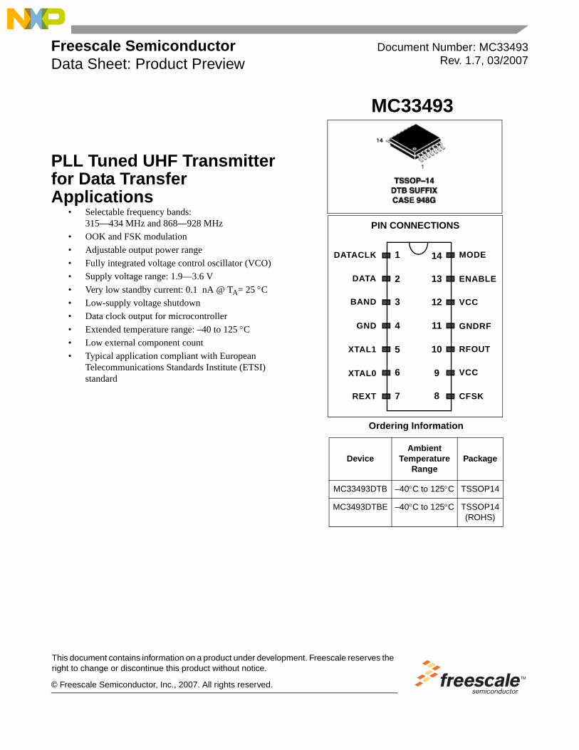
Applying a high-logic level on the MODE pin selects Frequency Shift Keying (FSK) modulation. This modulation is achieved by crystal pulling. An internal switch connected to the CFSK pin enables switching the external crystal load capacitors. Figure 2 shows the possible configurations: serial and parallel.
The logic level applied on pin DATA controls the state of this internal switch:DATA=0 → switch off,DATA=1 → switch on.
DATA input is internally re-synchronized by the crystal reference signal. The corresponding jitter on the data duty cycle cannot exceed ±1 reference period (±75 ns for a 13.56 MHz crystal).
This crystal pulling solution implies that the RF output frequency deviation equals the crystal frequency deviation multiplied by the PLL Divider ratio (see Table 3).
BAND Input LevelFrequency Band
(MHz)PLL Divider Ratio
Crystal OscillatorFrequency (MHz)
High 31532
9.84
43413.56
Low 868 64
PLL Tuned UHF Transmitter for Data Transfer Applications, Rev. 1.7
Freescale Semiconductor4
Microcontroller Interface
Figure 2. Crystal Pulling Configurations
5 Microcontroller InterfaceFour digital input pins (ENABLE, DATA, BAND, and MODE) enable the circuit to be controlled by a microcontroller. The band frequency and the modulation type should be configured before enabling the circuit.
One digital output pin, DATACLK, provides the microcontroller with a reference frequency for data clocking. This frequency is equal to the crystal oscillator frequency divided by 64 (see Table 4).
Table 4. DATACLK Frequency vs Crystal Oscillator Frequency
Crystal Oscillator Frequency (MHz) DATACLK Frequency (kHz)
9.84 15413.56 212
PLL Tuned UHF Transmitter for Data Transfer Applications, Rev. 1.7
Freescale Semiconductor 5
State Machine
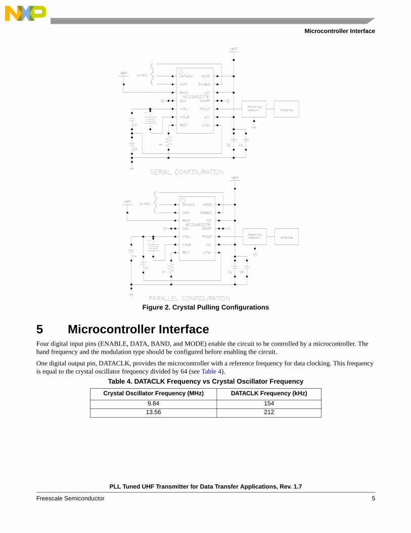
6 State MachineFigure 3 details the state machine.
Figure 3. State machine
State 1: The circuit is in standby mode and draws only a leakage current from the power supply.
State 2: In this state, the PLL is out of the lock-in range; therefore, the RF output stage is switched off, preventing RF transmission. Data clock is available on the DATACLK pin. Each time the device is enabled, the state machine passes through this state.
State 3: In this state, the PLL is within the lock-in range. If t < tPLL_lock_in, the PLL may be in acquisition mode. If t≥tPLL_lock_in, then the PLL is locked. Data entered on the DATA pin are output on the RFOUT pin according to the modulation selected by the level applied on the MODE pin.
State 4: When the supply voltage falls below the shutdown voltage threshold (VSDWN,) the entire circuit switches off. After this shutdown, applying a low level on the ENABLE pin unlatches the circuit.
Figure 4 shows the waveforms of the main signals for a typical application cycle.
State 2PLL out of lock-in range
No RF output
State 1Standby mode
ENABLE=1
PLL inlock-in range
Vbattery < Vshutdown
ENABLE=0
Power ONAND ENABLE=0
State 3Transmission mode
ENABLE=0
State 4Shutdown mode
PLL out oflock-in range
PLL Tuned UHF Transmitter for Data Transfer Applications, Rev. 1.7
Freescale Semiconductor6

Power Management
Figure 4. Signals Waveform and Timing Definition
7 Power ManagementWhen the battery voltage falls below the shutdown voltage threshold (VSDWN) the entire circuit switches off. After this shutdown, the circuit is latched until a low level is applied on pin ENABLE (see State 4 of the state machine).
8 Data ClockAt start-up, data clock timing is valid after the data clock settling time. Because the clock is switched off asynchronously, the last period duration cannot be guaranteed.
9 Electrical CharacteristicsUnless otherwise specified, voltage range Vcc=[Vshutdown;3.6 V], temperature range TA=[–40 °C;+ 125 °C], Rext=12 kΩ ± 5%, RF output frequency fcarrier = 433.92 MHz, reference frequency freference = 13.560 MHz, output load RL = 50 Ω ±1% (Figure 9). Values refer to the circuit shown in the recommended application schematics: Figure 12 shows OOK modulation and Figure 14 shows FSK modulation. Typical values reflect average measurement at VCC =3 V, TA = 25 °C.
ENABLE
DATACLK
DATA
State 1 State 2 State 3
tDATACLK_settling > tPLL_lock_in
tPLL_lock_in
MODE=0 (OOK)
MODE=1 (FSK)
State 1
fcarrierfcarrier
fhighflow fhighflow
: PLL locked
fhigh
RFOUT
PLL Tuned UHF Transmitter for Data Transfer Applications, Rev. 1.7
Freescale Semiconductor 7

Electrical Characteristics
Table 5. Electrical Characteristics
Parameter Test Conditions, CommentsLimits
UnitMin. Typ. Max.
1 General Parameters
1.1 Supply current instandby mode
TA ≤ 25 °C — 0.1 5 nA
1.2 TA = 60 °C — 7 30 nA
1.3 TA = 85 °C — 40 100 nA
1.4 TA = 125 °C — 800 1700 nA
1.5Supply current in
transmission mode315 and 434 bands,
OOK and FSK modulation,continuous wave, TA = 25 °C
— 11.6 13.5 mA
1.6 315 and 434 bands,DATA=0, –40 °C ≤ TA ≤ 125 °C
— 4.4 6.0 mA
1.7 868 MHz band,DATA=0, –40 °C ≤ TA ≤ 125 °C
— 4.6 6.2 mA
1.8315 and 434 bands,
OOK and FSK modulation,continuous wave, –40 °C ≤ TA ≤125 °C
— 11.6 14.9 mA
1.9868 MHz band,
OOK and FSK modulation,continuous wave, –40 °C ≤T A ≤ 125 °C
— 11.8 15.1 mA
1.10 Supply voltage — 3 3.6 V
1.11 Shutdown voltage threshold TA = –40 °C — 2.04 2.11 V
1.12 TA = –20 °C — 1.99 2.06 V
1.13 TA = 25 °C — 1.86 1.95 V
1.14 TA = 60 °C — 1.76 1.84 V
1.15 TA = 85 °C — 1.68 1.78 V
1.16 TA = 125 °C — 1.56 1.67 V
2 RF Parameters
2.1 Rext value 12 — 21 kΩ
2.2 Output power 315 and 434 MHz bands,with 50 Ω matching network
— 5 — dBm
2.3 868 MHz band,with 50 Ω matching network
— 1 — dBm
2.4 315 and 434 MHz bands,–40 °C ≤ TA ≤ 125 °C
–3 0 3 dBm
2.8 868 MHz band,–40 °C ≤TA ≤ 125 °C
–7 –3 0 dBm
2.12 Current and output powervariation vs. Rext value
315 and 434 MHz bands,with 50 Ω matching network
— –0.35–0.25
— dB/kΩmA/kΩ
PLL Tuned UHF Transmitter for Data Transfer Applications, Rev. 1.7
Freescale Semiconductor8

Electrical Characteristics
2.13 Harmonic 2 level 315 and 434 MHz bands,with 50 Ω matching network
— –34 — dBc
2.14 868 MHz band,with 50 Ω matching network
— –49 — dBc
2.15 315 and 434 MHz bands — –23 -17 dBc
2.16 868 MHz band — –38 -27 dBc
2.17 Harmonic 3 level 315 and 434 MHz bands,with 50 Ω matching network
— –32 — dBc
2.18 868 MHz band,with 50 Ω matching network
— –57 — dBc
2.19 315 and 434 MHz bands — –21 –15 dBc
2.20 868 MHz band — –48 –39 dBc
2.21 Spurious level @ fcarrier ± fDATACLK
315 and 434 MHz bands — –36 –24 dBc
2.22 868 MHz band — –29 –17 dBc
2.23 Spurious level @ fcarrier ± freference
315 MHz band — –37 –30 dBc
2.24 434 MHz band — –44 –34 dBc
2.25 868 MHz band — –37 –27 dBc
2.41 Spurious level @ fcarrier/2
315 MHz band — –62 –53 dBc
2.26 434 MHz band — –80 –60 dBc
2.27 868 MHz band — –45 –39 dBc
2.30 Phase noise 315 and 434 MHz bands,±175 kHz from fcarrier
— –75 –68 dBc/Hz
2.31 868 MHz band,±175 kHz from fcarrier
— –73 –66 dBc/Hz
2.32 PLL lock-in time,tPLL_lock_in
fcarrier within 30 kHz from the final value,crystal series resistor = 150 Ω
— 400 1600 µs
2.33 XTAL1 input capacitance — 1 — pF
2.34 Crystal resistance OOK modulation — 20 200 W
2.44 FSK modulation 20 50
2.35 OOK modulation depth 75 90 — dBc
2.36 FSK modulationcarrier frequency
total deviation
315 and 434 MHz bands, see note Note: — — 100 kHz
2.37 868 MHz band, see note Note: — — 200 kHz
2.38 CFSK output resistance MODE = 0, DATA = xMODE = 1, DATA = 0
50 70 — kΩ
2.39 MODE = 1, DATA = 1 — 90 300 W
2.43 CFSK output capacitance — 1 — pF
2.40 Data rate Manchester coding — — 10 kbit/s
Table 5. Electrical Characteristics (continued)
Parameter Test Conditions, CommentsLimits
UnitMin. Typ. Max.
PLL Tuned UHF Transmitter for Data Transfer Applications, Rev. 1.7
Freescale Semiconductor 9
RF Output Spectrum
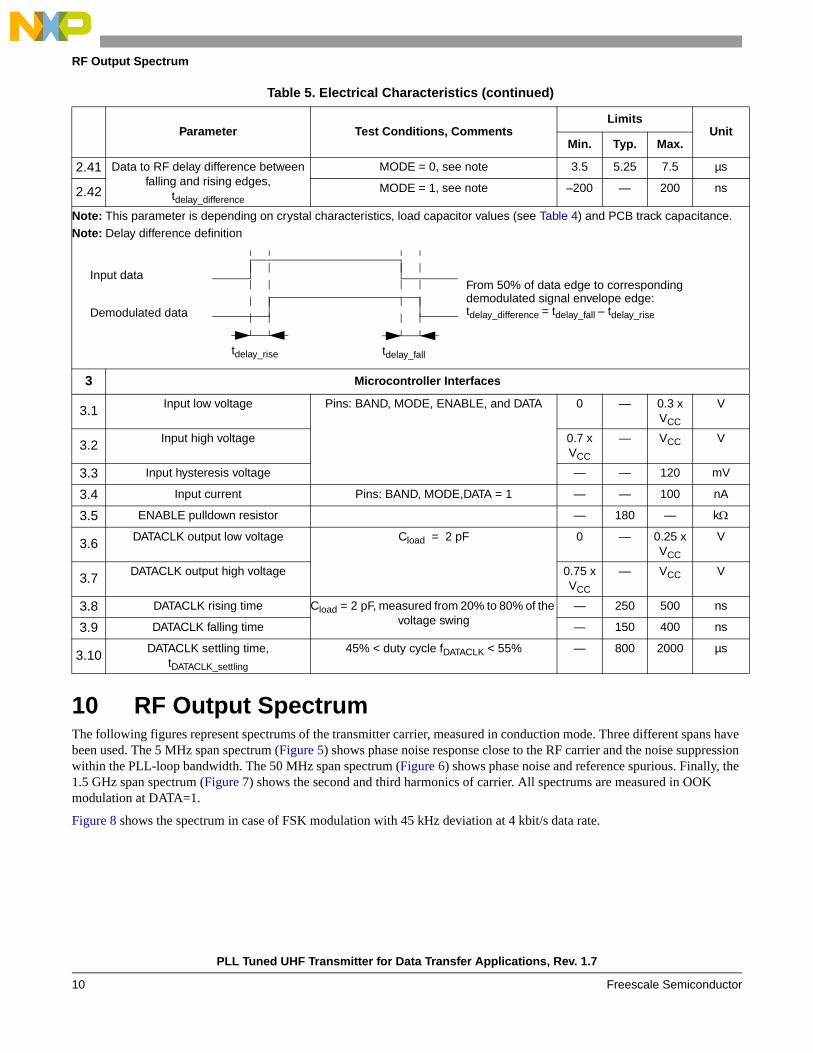
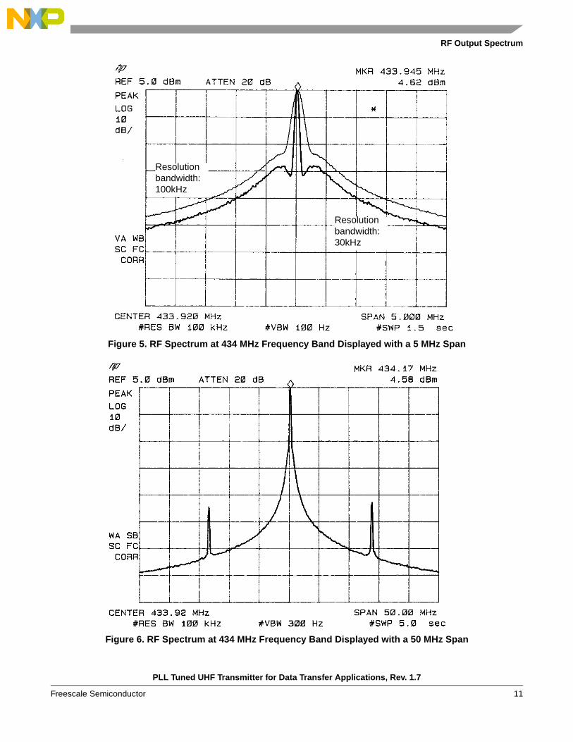
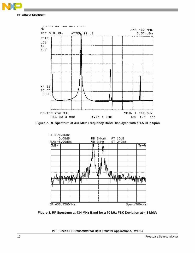
10 RF Output SpectrumThe following figures represent spectrums of the transmitter carrier, measured in conduction mode. Three different spans have been used. The 5 MHz span spectrum (Figure 5) shows phase noise response close to the RF carrier and the noise suppression within the PLL-loop bandwidth. The 50 MHz span spectrum (Figure 6) shows phase noise and reference spurious. Finally, the 1.5 GHz span spectrum (Figure 7) shows the second and third harmonics of carrier. All spectrums are measured in OOK modulation at DATA=1.
Figure 8 shows the spectrum in case of FSK modulation with 45 kHz deviation at 4 kbit/s data rate.
2.41 Data to RF delay difference between falling and rising edges,
tdelay_difference
MODE = 0, see note 3.5 5.25 7.5 µs
2.42 MODE = 1, see note –200 — 200 ns
Note: This parameter is depending on crystal characteristics, load capacitor values (see Table 4) and PCB track capacitance.
Note: Delay difference definition
3 Microcontroller Interfaces
3.1 Input low voltage Pins: BAND, MODE, ENABLE, and DATA 0 — 0.3 x VCC
V
3.2 Input high voltage 0.7 x VCC
— VCC V
3.3 Input hysteresis voltage — — 120 mV
3.4 Input current Pins: BAND, MODE,DATA = 1 — — 100 nA
3.5 ENABLE pulldown resistor — 180 — kΩ
3.6 DATACLK output low voltage Cload = 2 pF 0 — 0.25 x VCC
V
3.7 DATACLK output high voltage 0.75 x VCC
— VCC V
3.8 DATACLK rising time Cload = 2 pF, measured from 20% to 80% of the voltage swing
— 250 500 ns
3.9 DATACLK falling time — 150 400 ns
3.10 DATACLK settling time,tDATACLK_settling
45% < duty cycle fDATACLK < 55% — 800 2000 µs
Table 5. Electrical Characteristics (continued)
Parameter Test Conditions, CommentsLimits
UnitMin. Typ. Max.
Input data
Demodulated data
tdelay_rise tdelay_fall
From 50% of data edge to corresponding
tdelay_difference = tdelay_fall – tdelay_rise
demodulated signal envelope edge:
PLL Tuned UHF Transmitter for Data Transfer Applications, Rev. 1.7
Freescale Semiconductor10
RF Output Spectrum
Figure 5. RF Spectrum at 434 MHz Frequency Band Displayed with a 5 MHz Span
Figure 6. RF Spectrum at 434 MHz Frequency Band Displayed with a 50 MHz Span
Resolutionbandwidth:100kHz
Resolutionbandwidth:30kHz
PLL Tuned UHF Transmitter for Data Transfer Applications, Rev. 1.7
Freescale Semiconductor 11
RF Output Spectrum
Figure 7. RF Spectrum at 434 MHz Frequency Band Displayed with a 1.5 GHz Span
Figure 8. RF Spectrum at 434 MHz Band for a 70 kHz FSK Deviation at 4.8 kbit/s
PLL Tuned UHF Transmitter for Data Transfer Applications, Rev. 1.7
Freescale Semiconductor12

Output Power Measurement
11 Output Power MeasurementThe RF output levels given in Section 9, “Electrical Characteristics,” are measured with a 50 Ω load directly connected to the RFOUT pin, as shown below in Figure 9. This wideband coupling method gives results independent of the application.
Figure 9. Output Power Measurement Configurations
The configuration shown in Figure 10(a) provides better efficiency in terms of output power and harmonics rejection. The schematic on Figure 10(b) gives the equivalent circuit of the RFOUT pin and the DC bias impeder as well as matching network components for 434 MHz frequency band.
Figure 10. Output Model and Matching Network for 434 MHz Band
RFOUT RF output
RL= 50 W100 pF
Impeder: TDK MMZ1608Y102CTA00
VCC
RFOUT RF output
RL=50 Ω
Impeder: TDK MMZ1608Y102CTA00
VCC
MatchingNetwork
C0 R0 RL
L1
1.5 pF 250 Ω
3 kΩ 50 Ω
Matching
330pF
C3
39 nH
RFOUT pinLoadImpeder
(a)
(b)
Network
Ri
PLL Tuned UHF Transmitter for Data Transfer Applications, Rev. 1.7
Freescale Semiconductor 13

Complete Application Schematic and PCB for OOK Modulation
Figure 11 shows the output power versus the Rext resistor value with 50 Ω load and with matching network.
Figure 11. Output Power at 434 MHz Band vs Rext Value
The 50 Ω matching network used for the 868 MHz band is similar to the 434 MHz, excepting components values: L1 is changed to 8.2 nH and C3 to 470 pF in Figure 11. The typical gain of this 868 MHz matching network is 4 dB compared to unmatched configuration.
12 Complete Application Schematic and PCB for OOK Modulation
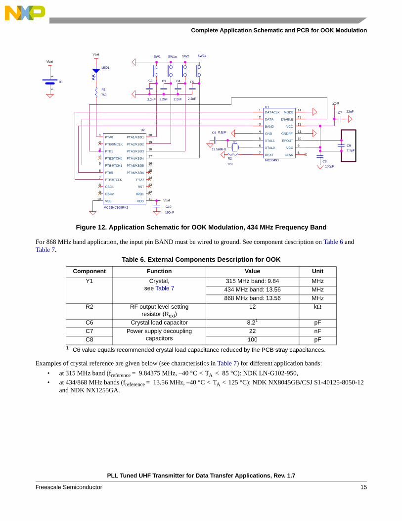
Figure 12 shows a complete application schematic using a MC68HC908RK2 microcontroller. OOK modulation is selected, fcarrier = 433.92 MHz. The C2 to C5 capacitors can be removed if switch debounce is done by software.
Output power measurement in typical conditions (434MHz - Vcc=3V - 25°C)
Output power when matched (dBm)
-0.35dB/kΩΩΩΩ # -0.35mA/kΩΩΩΩ
Output power on 50ΩΩΩΩ load (dBm)
-6
-4
-2
0
2
4
6
8
6 9 12 15 18 21 24
Rext (kΩΩΩΩ)
RFOUT
Level (dBm)
REXT SPECIFIED RANGE
PLL Tuned UHF Transmitter for Data Transfer Applications, Rev. 1.7
Freescale Semiconductor14
Complete Application Schematic and PCB for OOK Modulation
Figure 12. Application Schematic for OOK Modulation, 434 MHz Frequency Band
For 868 MHz band application, the input pin BAND must be wired to ground. See component description on Table 6 and Table 7.
Table 6. External Components Description for OOK
Examples of crystal reference are given below (see characteristics in Table 7) for different application bands:• at 315 MHz band (freference = 9.84375 MHz, –40 °C < TA < 85 °C): NDK LN-G102-950,• at 434/868 MHz bands (freference = 13.56 MHz, –40 °C < TA < 125 °C): NDK NX8045GB/CSJ S1-40125-8050-12
and NDK NX1255GA.
Component Function Value Unit
Y1 Crystal,see Table 7
315 MHz band: 9.84 MHz
434 MHz band: 13.56 MHz868 MHz band: 13.56 MHz
R2 RF output level settingresistor (Rext)
12 kΩ
C6 Crystal load capacitor 8.21
1 C6 value equals recommended crystal load capacitance reduced by the PCB stray capacitances.
pF
C7 Power supply decoupling capacitors
22 nFC8 100 pF
Vbat
Vbat
Vbat
Vbat
SW1 SW2 SW2aSW1a
C6 8.2pF
C3
2.2nF
C2
2.2nF
C5
2.2nF
C4
2.2nF
C7 22nF
R1
750
Y1
13.56MHz
LED1
C9
2.2pF
C8
100pF
R2
12K
B1
12
U2
MC68HC908RK2
PTA01
PTB0/MCLK2
PTB13
PTB2/TCH04
PTB4/TCH15
PTB56
PTB3/TCLK7
OSC18
OSC29
VSS10
VDD11
IRQ112
RST13
PTA714
PTA6/KBD615
PTA5/KBD516
PTA4/KBD417
PTA3/KBD318
PTA2/KBD219
PTA1/KBD120
C10
100nF
U1
MC33493
DATACLK1
DATA2
BAND3
GND4
XTAL15
XTAL06
REXT7
CFSK8
VCC9
RFOUT10
GNDRF11
VCC12
ENABLE13
MODE14
PLL Tuned UHF Transmitter for Data Transfer Applications, Rev. 1.7
Freescale Semiconductor 15

Complete Application Schematic and PCB for FSK Modulation
)
Figure 13 shows a two-button keyfob board. Size is 30 × 45 millimeters.
Figure 13. Two-Button Keyfob Board Layout
13 Complete Application Schematic and PCB for FSK Modulation
Figure 14 shows a complete application schematic using a MC68HC908RK2 microcontroller. FSK modulation is selected, fcarrier= 433.92 MHz. C1 capacitor can be removed if switch debounce is done by software.
Table 7. Typical Crystal Characteristics (SMD Package)
ParameterNDK LN-G102-950
(for 315 MHz)
NDK NX8045GB/CSJS1-40125-8050-12
(for 434 MHz and 868 MHz)
NDK NX1255GA(for 434 MHz and 868 MHz)
Unit
Load capacitance 12 12 12 pF
Motional capacitance 3.33 4.4 10.5 fF
Static capacitance 1.05 1.5 2.46 pF
Loss resistance 28 18.5 10 Ω
PLL Tuned UHF Transmitter for Data Transfer Applications, Rev. 1.7
Freescale Semiconductor16

Complete Application Schematic and PCB for FSK Modulation
Figure 14. Application Schematic for FSK Modulation, Serial Configuration, 434 MHz Frequency Band
For 868 MHz band application, the input pin BAND must be wired to ground. See component description in Table 8.
Figure 15 shows the corresponding PCB layout.
Table 8. External Components Description for FSK
Component Function Value Unit
Y1 Crystal 315 MHz band: 9.84,See Table 7
MHz
434 MHz band: 13.56,see Table 7
MHz
868 MHz band: 13.56,see Table 7
MHz
R1 RF output level settingresistor (Rext)
12 kΩ
C3 Crystal load capacitor See Table 9 pF
C4 pF
C2 Power supply decoupling capacitor 22 nF
C6 100 pF
PLL Tuned UHF Transmitter for Data Transfer Applications, Rev. 1.7
Freescale Semiconductor 17

Recommendations for FSK Modulation
Figure 15. Application PCB Layout for FSK Modulation, Serial Configuration, 434 MHz Frequency Band
Table 9 gives the measured FSK deviations respective to C3 and C4 capacitor values for three deviations. Crystal reference is NDK NX8045GB/CSJ S1-40125-8050-12.
Another crystal reference, NDK NX1255GA (see Table 7), is enabled to reach higher deviation as mentioned on Table 10. These results are due to the higher crystal motional capacitor.
14 Recommendations for FSK ModulationFSK deviation is function of total load capacitance presented to the crystal. This load capacitance is constituted by various contributors:
• the crystal characteristic, especially its static capacitance• the external load capacitors (C3, C4 as defined in Figure 14 and Table 9)• the device internal capacitance of pins XTAL0, XTAL1, CFSK• the PCB track capacitance
The schematic given in Figure 16 shows a typical FSK application using serial capacitor configuration, where device pads and PCB track capacitances are mentioned.
Table 9. Crystal Pulling Capacitor Values vs Carrier Frequency Total Deviation -1-
Carrier frequency(MHz)
Carrier frequency total deviation (kHz)
C3 capacitor (pF) C4 capacitor (pF)Recommended R_off value (kΩ)
434 45 4.7 6.8 10
70 2.2 10 —
100 1 15 22
868 90 4.7 6.8 10
140 2.2 10 —
200 1 15 22
Table 10. Crystal Pulling Capacitor Values vs Carrier Frequency Total Deviation -2-
Carrier frequency(MHz)
Carrier frequency total deviation (kHz)
C3 capacitor value (pF)
C4 capacitor value (pF)
Recommended R_off value (kΩ)
434 150 1 27 —
868 300 1 27 —
PLL Tuned UHF Transmitter for Data Transfer Applications, Rev. 1.7
Freescale Semiconductor18

Recommendations for FSK Modulation
Device pad capacitance is defined by the package capacitance and by the internal circuitry. Typical capacitance values for these pads are given in Table 11.
Some realistic assumptions and measurements have been made concerning track parasitic capacitances for a 0.8 mm FR4 double side application PCB. They are given in Table 11 and the corresponding PCB layout is shown in figure Figure 17.
To achieve large deviations, this total load capacitance must be lowered. For a given crystal, the PCB must be carefully laid out to reduce the capacitance of the tracks wired to XTAL0, XTAL1, and CFSK pins.
Recommendation: a R_off resistor can be added in parallel with the FSK switch to optimize the transient response of demodulated signal. Table 11 gives the optimized R_off values for two deviations. There is no footprint for R_off resistor on the layout in Figure 16. When used, this component can be soldered on top of C3.
Figure 16. Crystal Load Capacitance Contributors Schematic
Table 11. Pads and Tracks Parasitic Values
Capacitance Value Unit
C_pad_XTAL0 1 pF
C_pad_XTAL1 1 pF
C_pad_CFSK 1 pF
C_track_XTAL0 1.5 pF
C_track_XTAL1 1.5 pF
C_track_CFSK 1.5 pF
PLL Tuned UHF Transmitter for Data Transfer Applications, Rev. 1.7
Freescale Semiconductor 19

Case Outline Dimensions
15 Case Outline Dimensions
Figure 17. Case Outline Dimensions
CASE 948G-01ISSUE O
DIM MIN MAX MIN MAXINCHESMILLIMETERS
A 4.90 5.10 0.193 0.200B 4.30 4.50 0.169 0.177C --- 1.20 --- 0.047D 0.05 0.15 0.002 0.006F 0.50 0.75 0.020 0.030G 0.65 BSC 0.026 BSCH 0.50 0.60 0.020 0.024J 0.09 0.20 0.004 0.008
J1 0.09 0.16 0.004 0.006K 0.19 0.30 0.007 0.012
K1 0.19 0.25 0.007 0.010L 6.40 BSC 0.252 BSCM 0 8 0 8
NOTES:1. DIMENSIONING AND TOLERANCING PER
ANSI Y14.5M, 1982.2. CONTROLLING DIMENSION: MILLIMETER.3. DIMENSION A DOES NOT INCLUDE MOLD
FLASH, PROTRUSIONS OR GATE BURRS. MOLD FLASH OR GATE BURRS SHALL NOT EXCEED 0.15 (0.006) PER SIDE.
4. DIMENSION B DOES NOT INCLUDE INTERLEAD FLASH OR PROTRUSION. INTERLEAD FLASH OR PROTRUSION SHALL NOT EXCEED0.25 (0.010) PER SIDE.
5. DIMENSION K DOES NOT INCLUDE DAMBAR PROTRUSION. ALLOWABLE DAMBAR PROTRUSION SHALL BE 0.08 (0.003) TOTAL IN EXCESS OF THE K DIMENSION AT MAXIMUM MATERIAL CONDITION.
6. TERMINAL NUMBERS ARE SHOWN FOR REFERENCE ONLY.
7. DIMENSION A AND B ARE TO BE
° ° ° °
SU0.15 (0.006)T
2X L/2
SUM0.10 (0.004) V ST
L-U-
SEATINGPLANE
0.10 (0.004)-T-
SECTION N-N
DETAIL E
J J1
KK1
DETAIL E
F
M
-W-
0.25 (0.010)814
71
PIN 1IDENT.
HG
A
D
C
B
SU0.15 (0.006)T
-V-
14X REFK
N
N
PLL Tuned UHF Transmitter for Data Transfer Applications, Rev. 1.7
Freescale Semiconductor20
THIS PAGE INTENTIONALLY BLANK
PLL Tuned UHF Transmitter for Data Transfer Applications, Rev. 1.7
Freescale Semiconductor 21

Document Number: MC33493Rev. 1.703/2007
How to Reach Us:
Home Page:www.freescale.com
Web Support:http://www.freescale.com/support
USA/Europe or Locations Not Listed:Freescale Semiconductor, Inc.Technical Information Center, EL5162100 East Elliot RoadTempe, Arizona 85284+1-800-521-6274 or +1-480-768-2130www.freescale.com/support
Europe, Middle East, and Africa:Freescale Halbleiter Deutschland GmbHTechnical Information CenterSchatzbogen 781829 Muenchen, Germany+44 1296 380 456 (English)+46 8 52200080 (English)+49 89 92103 559 (German)+33 1 69 35 48 48 (French)www.freescale.com/support
Japan:Freescale Semiconductor Japan Ltd.HeadquartersARCO Tower 15F1-8-1, Shimo-Meguro, Meguro-ku,Tokyo 153-0064Japan0120 191014 or +81 3 5437 [email protected]
Asia/Pacific:Freescale Semiconductor Hong Kong Ltd.Technical Information Center2 Dai King StreetTai Po Industrial EstateTai Po, N.T., Hong Kong+800 2666 [email protected]
For Literature Requests Only:Freescale Semiconductor Literature Distribution CenterP.O. Box 5405Denver, Colorado 802171-800-441-2447 or 303-675-2140Fax: [email protected]
Information in this document is provided solely to enable system and software implementers to use Freescale Semiconductor products. There are no express or implied copyright licenses granted hereunder to design or fabricate any integrated circuits or integrated circuits based on the information in this document.
Freescale Semiconductor reserves the right to make changes without further notice to any products herein. Freescale Semiconductor makes no warranty, representation or guarantee regarding the suitability of its products for any particular purpose, nor does Freescale Semiconductor assume any liability arising out of the application or use of any product or circuit, and specifically disclaims any and all liability, including without limitation consequential or incidental damages. “Typical” parameters that may be provided in Freescale Semiconductor data sheets and/or specifications can and do vary in different applications and actual performance may vary over time. All operating parameters, including “Typicals”, must be validated for each customer application by customer’s technical experts. Freescale Semiconductor does not convey any license under its patent rights nor the rights of others. Freescale Semiconductor products are not designed, intended, or authorized for use as components in systems intended for surgical implant into the body, or other applications intended to support or sustain life, or for any other application in which the failure of the Freescale Semiconductor product could create a situation where personal injury or death may occur. Should Buyer purchase or use Freescale Semiconductor products for any such unintended or unauthorized application, Buyer shall indemnify and hold Freescale Semiconductor and its officers, employees, subsidiaries, affiliates, and distributors harmless against all claims, costs, damages, and expenses, and reasonable attorney fees arising out of, directly or indirectly, any claim of personal injury or death associated with such unintended or unauthorized use, even if such claim alleges that Freescale Semiconductor was negligent regarding the design or manufacture of the part.
RoHS-compliant and/or Pb-free versions of Freescale products have the functionality and electrical characteristics as their non-RoHS-compliant and/or non-Pb-free counterparts. For further information, see http://www.freescale.com or contact your Freescale sales representative.
For information on Freescale’s Environmental Products program, go to http://www.freescale.com/epp.
Freescale™ and the Freescale logo are trademarks of Freescale Semiconductor, Inc. All other product or service names are the property of their respective owners.The Power Architecture and Power.org word marks and the Power and Power.org logos and related marks are trademarks and service marks licensed by Power.org
© Freescale Semiconductor, Inc. 2007. All rights reserved.


![EC0804-PLL [Modo de compatibilidad]€¦ · (PLL) 1 Capítulo 4 Lazos enganchados en fase. PLL Aplicaciones de los PLL Síntesis de frecuencia Partiendo de un oscilador patrón (f0),](https://img.dokumen.tips/doc/110x75/5e8e438d8741af3761030a0b/ec0804-pll-modo-de-compatibilidad-pll-1-captulo-4-lazos-enganchados-en-fase.jpg)