Embed Size (px)
Citation preview

M. Krishna Kumar MAM/M1/LU4/V1/2004 1
Pin Diagram of 8085
20
19181716
1514
13
1211
1
2345678
910
21
2223
242526272829
30
403938373635343332
31
8085 A
VSS
AD7
AD6
AD5
X1X2
OUTSODSIDTRAPRST 7.5RST 6.5RST 5.5INTR_____
INTAAD0
AD1
AD2
AD3
AD4
RESET
A8
VccHOLDHLDACLK ( OUT) _________________
RESET IN
S1___
RD
ALES0
READY __
IO / M
___
WR
A9
A10
A11
A15
A14
A13
A12
Serial i/p, o/p signals
DMA

M. Krishna Kumar MAM/M1/LU4/V1/2004 2
Signal Groups of 8085
Multiplexed address / data bus
GND
VssVcc
+ 5 V
X1 X2
XTAL
4
5
SOD
SID
RESET OUT CLK OUT
____
WR
____
RD
___
IO / M
S0
S1
ALE
A8
A15High order Address bus
AD0
AD7
HLDA______
INTA
READYHOLD ______________
RESET IN
INTRRESET 5.5RESET 6.5RESET 7.5
TRAP

M. Krishna Kumar MAM/M1/LU4/V1/2004 3
GND
+5V
X1
X2
TIMING AND CONTROLCLK
GEN
CLK OUT READY
CONTROL
RD
ALE
S0 S1 RESET OUT
IO / M HOLD HLDA
DMASTATUS
RESET IN
ARITHEMETIC LOGIC UNIT ( ALU)
(8)
ACCUMULATOR TEMP REG(8)
(8)
FLAG ( 5)
FLIP FLOPS
INTERRUPT CONTROL SERIAL I / O CONTROL
SID SIOTRAP
INTR
INTA RES
5 . 5
RES
6 . 5
RES
7 . 5
8 BIT INTERNAL DATA BUS
INSTRUCTION REGISTER ( 8 )
MULTIPLXER
R
E
G.
S
E
L
E
C
T
ADDRESS BUFFER ( 8 )
DATA / ADDRESS BUFFER ( 8 )
INSTRUCTION DECODER AND MACHINE ENCODING
W ( 8 )
TEMP . REG.B REG ( 8 )
D REG ( 8 )H REG ( 8 )
STACK POINTERPROGRAM COUNTER ( 16 )INCREAMENT / DECREAMENT
ADDRESS LATCH ( 16 )
( 16 )
AD7 – AD0 ADDRESS / BUFFER BUS
A 15 – A8 ADDRESS BUS
C REG ( 8 )
E REG ( 8 )L REG ( 8 )
WR

M. Krishna Kumar MAM/M1/LU4/V1/2004 4
CYPACS Z
D0D1D2D3D4D5D6D7
Flag Registers
General Purpose RegistersINDIVIDUAL
COMBININATON
B, C, D, E, H, L
B & C, D & E, H & L

M. Krishna Kumar MAM/M1/LU4/V1/2004 5
AH AL
BH BL
CH CL
DH DL
SP
BP
SI
DI
ES
CS
SS
DS
IP
1
∑ADDRESS BUS
( 20 ) BITS
DATA BUS
( 16 ) BITS
BUS
CONTROL LOGIC
8
0
8
6
BUS
2 3 4 65
INSTRUCTION QUEUE
8 BIT
Q BUS
EU CONTROL SYSTEM
ALU DATA BUS
16 BITS
TEMPORARY REGISTERS
ALU
FLAGS
GENERAL REGISTERS
EXECUTION UNIT ( EU )
BUS INTERFACE UNIT ( BIU)
Fig:

M. Krishna Kumar MAM/M1/LU4/V1/2004 6
20
19181716
1514
13
1211
1
2345678
910
21
2223
242526272829
30
403938373635343332
31
8086
CPU
GND
CLK
INTR
NMI
GNDAD14
AD13
AD12
AD11
AD10
AD9AD8AD7
AD6
AD5
AD4
AD3
AD2
AD1
AD0
RESET
VCC
AD15
A16 / S3
A17 / S4
____
MN/MX___
RD
_______
LOCK
A19/S6
___
(WR)
READY
______
TEST
QS1
____
S2___
S1 _____
(DEN)(ALE)
A18 / S5
_____
BHE / S7
_____ _____
RQ / GT0 ( HOLD)___ _____
RQ / GT1 ( HLDA)____
(M / IO )___
(DT / R)___
S0 QS0 ________
(INTA)
Pin Diagram of 8086
M. Krishna Kumar MAM/M1/LU4/V1/2004 7
CLK
GNDVCC
8086
MPU
INTR_____
INTA
______
TEST
NMI
RESET
HOLD
HLDA
VCC
____
MN / MX
INTERRUPT
INTERFACE
DMA
INTERFACE
MODE SELECT READY
_____
DEN
_____
WR
____
RD
__
DT / R
__
M / IO
ALE___
BHE / S7
MEMORY I / O
CONTROLS
D0 - D15
A0 - A15, A16 / S3 – A19/S6
ADDRESS / DATA BUS
M. Krishna Kumar MAM/M1/LU4/V1/2004 8
Signal Description of 8086
• The Microprocessor 8086 is a 16-bit CPU available in different clock rates and packaged in a 40 pin CERDIP or plastic package.
• The 8086 operates in single processor or multiprocessor configuration to achieve high performance. The pins serve a particular function in minimum mode (single processor mode ) and other function in maximum mode configuration (multiprocessor mode ).
• The 8086 signals can be categorised in three groups. The first are the signal having common functions in minimum as well as maximum mode.

M. Krishna Kumar MAM/M1/LU4/V1/2004 9
• The second are the signals which have special functions for minimum mode and third are the signals having special functions for maximum mode.
• The following signal descriptions are common for both modes.• AD15-AD0 : These are the time multiplexed memory I/O
address and data lines.• Address remains on the lines during T1 state, while the data is
available on the data bus during T2, T3, Tw and T4.• These lines are active high and float to a tristate during
interrupt acknowledge and local bus hold acknowledge cycles.
Signal Description of 8086 (cont..)

M. Krishna Kumar MAM/M1/LU4/V1/2004 10
• A19/S6,A18/S5,A17/S4,A16/S3 : These are the time multiplexed address and status lines.
• During T1 these are the most significant address lines for memory operations.
• During I/O operations, these lines are low. During memory or I/O operations, status information is available on those lines for T2,T3,Tw and T4.
• The status of the interrupt enable flag bit is updated at the beginning of each clock cycle.
Signal Description of 8086 (cont..)

M. Krishna Kumar MAM/M1/LU4/V1/2004 11
• The S4 and S3 combinedly indicate which segment register is presently being used for memory accesses as in below fig.
• These lines float to tri-state off during the local bus hold acknowledge. The status line S6 is always low .
• The address bit are separated from the status bit using latches controlled by the ALE signal.
Alternate DataStack
Code or noneData
Indication S4 S3
0011
0
01
1
Signal Description of 8086 (cont..)

M. Krishna Kumar MAM/M1/LU4/V1/2004 12
• BHE/S7 : The bus high enable is used to indicate the transfer of data over the higher order ( D15-D8 ) data bus as shown in table. It goes low for the data transfer over D15-D8 and is used to derive chip selects of odd address memory bank or peripherals. BHE is low during T1 for read, write and interrupt acknowledge cycles, whenever a byte is to be transferred on higher byte of data bus. The status information is available during T2, T3 and T4. The signal is active low and tristated during hold. It is low during T1 for the first pulse of the interrupt acknowledge cycle.
Upper byte from or to odd addressWhole word0
01
0
01
Lower byte from or to even addressUpper byte from or to even address
None
Indication BHE A0
1 1
Signal Description of 8086 (cont..)

M. Krishna Kumar MAM/M1/LU4/V1/2004 13
• RD – Read : This signal on low indicates the peripheral that the processor is performing s memory or I/O read operation. RD is active low and shows the state for T2, T3, Tw of any read cycle. The signal remains tristated during the hold acknowledge.
• READY : This is the acknowledgement from the slow device or memory that they have completed the data transfer. The signal made available by the devices is synchronized by the 8284A clock generator to provide ready input to the 8086. the signal is active high.
Signal Description of 8086 (cont..)

M. Krishna Kumar MAM/M1/LU4/V1/2004 14
• INTR-Interrupt Request : This is a triggered input. This is sampled during the last clock cycles of each instruction to determine the availability of the request. If any interrupt request is pending, the processor enters the interrupt acknowledge cycle.
• This can be internally masked by resulting the interrupt enable flag. This signal is active high and internally synchronized.
• TEST : This input is examined by a ‘WAIT’ instruction. If the TEST pin goes low, execution will continue, else the processor remains in an idle state. The input is synchronized internally during each clock cycle on leading edge of clock.
Signal Description of 8086 (cont..)

M. Krishna Kumar MAM/M1/LU4/V1/2004 15
• NMI- Nonmaskable interrupt : This is an edge triggered input which causes a Type 2 interrupt. The NMI is not maskable internally by software. A transition from low to high initiates the interrupt response at the end of the current instruction. This input is internally synchronized.
• RESET : This input causes the processor to terminate the current activity and start execution from FFF0H. The signal is active high and must be active for at least four clock cycles. It restarts execution when the RESET returns low. RESET is also internally synchronized.
• Vcc +5V power supply for the operation of the internal circuit.• GND ground for internal circuit.
Signal Description of 8086 (cont..)

M. Krishna Kumar MAM/M1/LU4/V1/2004 16
• CLK- Clock Input : The clock input provides the basic timing for processor operation and bus control activity. Its an asymmetric square wave with 33% duty cycle.
• MN/MX : The logic level at this pin decides whether the processor is to operate in either minimum or maximum mode.
• The following pin functions are for the minimum modeoperation of 8086.
• M/IO – Memory/IO : This is a status line logically equivalent to S2 in maximum mode. When it is low, it indicates the CPU is having an I/O operation, and when it is high, it indicates that the CPU is having a memory operation. This line becomes active high in the previous T4 and remains active till final T4 of the current cycle. It is tristated during local bus “hold acknowledge “.
Signal Description of 8086 (cont..)

M. Krishna Kumar MAM/M1/LU4/V1/2004 17
• INTA – Interrupt Acknowledge : This signal is used as a read strobe for interrupt acknowledge cycles. i.e. when it goes low, the processor has accepted the interrupt.
• ALE – Address Latch Enable : This output signal indicates the availability of the valid address on the address/data lines,and is connected to latch enable input of latches. This signal is active high and is never tristated.
• DT/R – Data Transmit/Receive: This output is used to decide the direction of data flow through the transreceivers (bidirectional buffers). When the processor sends out data, thissignal is high and when the processor is receiving data, this signal is low.
Signal Description of 8086 (cont..)

M. Krishna Kumar MAM/M1/LU4/V1/2004 18
• DEN – Data Enable : This signal indicates the availability of valid data over the address/data lines. It is used to enable thetransreceivers ( bidirectional buffers ) to separate the data from the multiplexed address/data signal. It is active from the middle of T2 until the middle of T4. This is tristated during ‘hold acknowledge’ cycle.
• HOLD, HLDA- Acknowledge : When the HOLD line goes high, it indicates to the processor that another master is requesting the bus access.
• The processor, after receiving the HOLD request, issues the hold acknowledge signal on HLDA pin, in the middle of the next clock cycle after completing the current bus cycle.
Signal Description of 8086 (cont..)

M. Krishna Kumar MAM/M1/LU4/V1/2004 19
• At the same time, the processor floats the local bus and control lines. When the processor detects the HOLD line low, it lowers the HLDA signal. HOLD is an asynchronous input, and is should be externally synchronized.
• If the DMA request is made while the CPU is performing a memory or I/O cycle, it will release the local bus during T4provided :
1. The request occurs on or before T2 state of the current cycle.2. The current cycle is not operating over the lower byte of a
word. 3. The current cycle is not the first acknowledge of an interrupt
acknowledge sequence.
Signal Description of 8086 (cont..)

M. Krishna Kumar MAM/M1/LU4/V1/2004 20
4. A Lock instruction is not being executed.• The following pin function are applicable for maximum
mode operation of 8086.• S2, S1, S0 – Status Lines : These are the status lines which
reflect the type of operation, being carried out by the processor. These become activity during T4 of the previous cycle and active during T1 and T2 of the current bus cycles.
1 1
S2 S1 S0 Indication0
1
000
111
1
11
1
1
1
00 0
0
0
000
Interrupt AcknowledgeRead I/O portWrite I/O portHaltCode Access
PassiveWrite memoryRead memory
1 1
Signal Description of 8086 (cont..)

M. Krishna Kumar MAM/M1/LU4/V1/2004 21
• LOCK : This output pin indicates that other system bus master will be prevented from gaining the system bus, while the LOCK signal is low.
• The LOCK signal is activated by the ‘LOCK’ prefix instruction and remains active until the completion of the next instruction. When the CPU is executing a critical instruction which requires the system bus, the LOCK prefix instruction ensures that other processors connected in the system will not gain the control of the bus.
• The 8086, while executing the prefixed instruction, asserts thebus lock signal output, which may be connected to an external bus controller.
Signal Description of 8086 (cont..)

M. Krishna Kumar MAM/M1/LU4/V1/2004 22
• QS1, QS0 – Queue Status: These lines give information about the status of the code-prefetch queue. These are active during the CLK cycle after while the queue operation is performed.
• This modification in a simple fetch and execute architecture of a conventional microprocessor offers an added advantage of pipelined processing of the instructions.
• The 8086 architecture has 6-byte instruction prefetch queue. Thus even the largest (6-bytes) instruction can be prefetched from the memory and stored in the prefetch. This results in a faster execution of the instructions.
• In 8085 an instruction is fetched, decoded and executed and only after the execution of this instruction, the next one is fetched.
Signal Description of 8086 (cont..)

M. Krishna Kumar MAM/M1/LU4/V1/2004 23
• By prefetching the instruction, there is a considerable speedingup in instruction execution in 8086. This is known as instruction pipelining.
• At the starting the CS:IP is loaded with the required address from which the execution is to be started. Initially, the queue will be empty an the microprocessor starts a fetch operation to bring one byte (the first byte) of instruction code, if the CS:IP address is odd or two bytes at a time, if the CS:IP address is even.
• The first byte is a complete opcode in case of some instruction (one byte opcode instruction) and is a part of opcode, in case of some instructions ( two byte opcode instructions), the remaining part of code lie in second byte.
Signal Description of 8086 (cont..)

M. Krishna Kumar MAM/M1/LU4/V1/2004 24
• But the first byte of an instruction is an opcode. When the first byte from the queue goes for decoding and interpretation, one byte in the queue becomes empty and subsequently the queue is updated.
• The microprocessor does not perform the next fetch operation till at least two bytes of instruction queue are emptied. The instruction execution cycle is never broken for fetch operation.After decoding the first byte, the decoding circuit decides whether the instruction is of single opcode byte or double opcode byte.
• If it is single opcode byte, the next bytes are treated as data bytes depending upon the decoded instruction length, otherwise, the next byte in the queue is treated as the second byte of the instruction opcode.
Signal Description of 8086 (cont..)

M. Krishna Kumar MAM/M1/LU4/V1/2004 25
• The second byte is then decoded in continuation with the first byte to decide the instruction length and the number of subsequent bytes to be treated as instruction data.
• The queue is updated after every byte is read from the queue but the fetch cycle is initiated by BIU only if at least two bytes of the queue are empty and the EU may be concurrently executing the fetched instructions.
• The next byte after the instruction is completed is again the first opcode byte of the next instruction. A similar procedure is repeated till the complete execution of the program.
Signal Description of 8086 (cont..)

M. Krishna Kumar MAM/M1/LU4/V1/2004 26
• The fetch operation of the next instruction is overlapped with the execution of the current instruction. As in the architecture, there are two separate units, namely Execution unit and Bus interface unit.
• While the execution unit is busy in executing an instruction, after it is completely decoded, the bus interface unit may be fetching the bytes of the next instruction from memory, depending upon the queue status.
QS1 QS0 Indication0
1 11
10
00
No operationFirst byte of the opcode from the queueEmpty queueSubsequent byte from the queue
Signal Description of 8086 (cont..)

M. Krishna Kumar MAM/M1/LU4/V1/2004 27
• RQ/GT0, RQ/GT1 – Request/Grant : These pins are used by the other local bus master in maximum mode, to force the processor to release the local bus at the end of the processor current bus cycle.
• Each of the pin is bidirectional with RQ/GT0 having higher priority than RQ/GT1.
• RQ/GT pins have internal pull-up resistors and may be left unconnected.
• Request/Grant sequence is as follows:1. A pulse of one clock wide from another bus master requests
the bus access to 8086.
Signal Description of 8086 (cont..)

M. Krishna Kumar MAM/M1/LU4/V1/2004 28
2. During T4(current) or T1(next) clock cycle, a pulse one clock wide from 8086 to the requesting master, indicates that the 8086 has allowed the local bus to float and that it will enter the ‘hold acknowledge’ state at next cycle. The CPU bus interface unit is likely to be disconnected from the local bus of the system.
3. A one clock wide pulse from the another master indicates to the 8086 that the hold request is about to end and the 8086 may regain control of the local bus at the next clock cycle. Thus each master to master exchange of the local bus is a sequence of 3 pulses. There must be at least one dead clock cycle after each bus exchange.
Signal Description of 8086 (cont..)

M. Krishna Kumar MAM/M1/LU4/V1/2004 29
• The request and grant pulses are active low.• For the bus request those are received while 8086 is
performing memory or I/O cycle, the granting of the bus is governed by the rules as in case of HOLD and HLDA in minimum mode.
Signal Description of 8086

M. Krishna Kumar MAM/M1/LU4/V1/2004 30
General Bus Operation
• The 8086 has a combined address and data bus commonly referred as a time multiplexed address and data bus.
• The main reason behind multiplexing address and data over the same pins is the maximum utilisation of processor pins and it facilitates the use of 40 pin standard DIP package.
• The bus can be demultiplexed using a few latches and transreceivers, when ever required.
• Basically, all the processor bus cycles consist of at least fourclock cycles. These are referred to as T1, T2, T3, T4. The address is transmitted by the processor during T1. It is present on the bus only for one cycle.

M. Krishna Kumar MAM/M1/LU4/V1/2004 31
• During T2, i.e. the next cycle, the bus is tristated for changing the direction of bus for the following data read cycle. The datatransfer takes place during T3, T4.
• In case, an address device is slow ‘NOT READY’ status the wait status Tw are inserted between T3 and T4. These clock states during wait period are called idle states (Ti), wait states(Tw) or inactive states. The processor used these cycles for internal housekeeping.
• The address latch enable (ALE) signal is emitted during T1 by the processor (minimum mode) or the bus controller (maximum mode) depending upon the status of the MN/MX input.
General Bus Operation ( cont..)
M. Krishna Kumar MAM/M1/LU4/V1/2004 32
• The negative edge of this ALE pulse is used to separate the address and the data or status information. In maximum mode, the status lines S0, S1 and S2 are used to indicate the type of operation.
• Status bits S3 to S7 are multiplexed with higher order address bits and the BHE signal. Address is valid during T1 while status bits S3 to S7 are valid during T2 through T4.
General Bus Operation ( cont..)
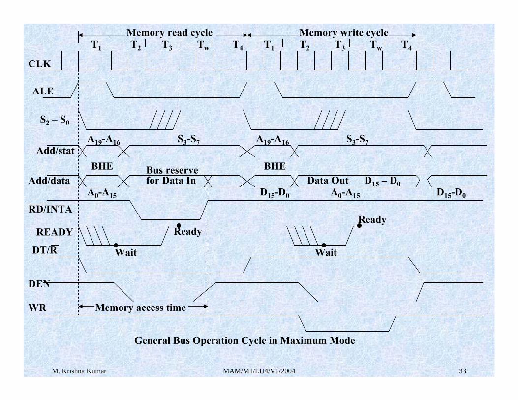
M. Krishna Kumar MAM/M1/LU4/V1/2004 33
General Bus Operation Cycle in Maximum Mode
CLK
Memory read cycle Memory write cycleT1 T2 T3 Tw T4 T1 T2 T3 Tw T4
ALE
S2 – S0
Add/stat
WR
DEN
DT/R
READY
RD/INTA
Add/data
A19-A16 S3-S7 A19-A16 S3-S7
BHE BHE
A0-A15 D15-D0 A0-A15 D15-D0
Bus reserveData Out D15 – D0
Wait Wait
ReadyReady
Memory access time
for Data In


![Wireless Starter Kit Mainboard - Silicon Labs · vcom_enable pti0[0..2] vmcu gnd gnd gnd gnd vmcu vrf 5v 3v3 gnd vrf gnd gnd gnd gnd gnd usb_vbus usb_vreg usb_vbus 5v 5v_dbg …](https://img.dokumen.tips/doc/110x75/5ac0fbea7f8b9a4e7c8c7c14/wireless-starter-kit-mainboard-silicon-labs-pti002-vmcu-gnd-gnd-gnd-gnd-vmcu.jpg)


![V^d]JdZV AD13 -10 PRO THAILAND J `:oJhwUZJdwZsJU](https://img.dokumen.tips/doc/110x75/61c04bff30b83a783127d6bc/vdjdzv-ad13-10-pro-thailand-j-ojhwuzjdwzsju.jpg)