Embed Size (px)
Citation preview

ARTICLE IN PRESS+ModelNANTOD-344; No. of Pages 24
Nano Today (2014) xxx, xxx—xxx
Available online at www.sciencedirect.com
ScienceDirect
j our na l ho me pag e: www.elsev ier .com/ locate /nanotoday
REVIEW
Piezotronics and piezo-phototronics — Fromsingle nanodevices to array of devices andthen to integrated functional system
Wenzhuo Wua, Caofeng Pana,b, Yan Zhanga,b, Xiaonan Wena,Zhong Lin Wanga,b,∗
a School of Materials Science and Engineering, Georgia Institute of Technology, Atlanta, GA 30332-0245,United Statesb Beijing Institute of Nanoenergy and Nanosystems, Chinese Academy of Sciences, China
Received 4 October 2013; received in revised form 19 November 2013; accepted 28 November 2013
KEYWORDSPiezopotential;Piezotronics;Piezo-phototronics;LED;Sensors
Summary Due to the polarization of ions in a crystal that has non-central symmetry inpiezoelectric-semiconductors such as ZnO, GaN and InN, piezoelectric polarization charges arecreated at the interface region by applying a strain, which created a potential (piezopotential)in the crystal. Piezotronics is about the devices fabricated using the piezopotential as a ‘‘gate’’voltage to tune/control charge carrier transport at a contact or junction. The piezo-phototroniceffect is to use the piezopotential to control the carrier generation, transport, separationand/or recombination for improving the performance of optoelectronic devices, such as solarcell and LED. Starting from the fundamental physics principles, this article gives an updated
review about the fabrication of array of piezotronic devices so that they can be integratedinto a system for achieving specific functions as sensors and MEMS. This first demonstration offabricating array of piezotronic devices and integrated them into a system is a major milestonein nanotechnology, and it represents one of the promising directions of nanoelectronics.ts re
© 2013 Elsevier Ltd. All righPlease cite this article in press as: W. Wu, et al., Nano Today (
∗ Corresponding author at: School of Materials Science and Engi-neering, Georgia Institute of Technology, Atlanta, GA 30332-0245,United States.
E-mail addresses: [email protected],[email protected] (Z.L. Wang).
I
Eacciems
1748-0132/$ — see front matter © 2013 Elsevier Ltd. All rights reserved.http://dx.doi.org/10.1016/j.nantod.2013.11.002
served.
ntroduction
nabling technologies for developing electronics with tun-ble functionalities are critical to emerging applications inonsumer electronics, prosthetic devices, robotics, surgi-al instruments and biomedical therapy/treatments [1—7],
2014), http://dx.doi.org/10.1016/j.nantod.2013.11.002
n which the active and adaptive interactions betweenlectronic devices and stimuli from the ambient environ-ent/host (e.g. human body) are essential. Mechanical
timuli are ubiquitous and abundant in the environment

IN PRESS+ModelN
2 W. Wu et al.
fmdtsclitsNpdnicbGpuroitli[sthfiotptaOssn
F
P
Zrodsoanfspnob
Figure 1 Strain-induced polarization in piezoelectric semi-conductor. (a) Left, distribution of piezopotential along aZnO NW under axial strain calculated by numerical meth-ods. (Reprinted with permission from [15]. Copyright 2009AIP Publishing LLC.) (b) Numerical calculation results of thepiezopotential distribution in an n-type ZnO NW consider-ing finite doping with donor concentration of 1 × 1017 cm−3.(Reprinted with permission from [17]. Copyright 2009 Ameri-can Chemical Society.). (c) Numerical calculation results of thepiezopotential distribution when the acceptor concentration inthe ZnO NW is 1 × 1017 cm−3. (Reprinted with permission from[20]. Copyright 2009 American Chemical Society.) The color gra-dient represents the distribution of piezopotential in which redindicates positive piezopotential and blue indicates negativepiezopotential. The growth direction of the NW is along c-axis.(e
dw
tpAecTttisoet
ARTICLEANTOD-344; No. of Pages 24
or interacting with or controlling the electronics inicro/nano-systems [8—10]. It is, however, not facile toirectly interface mechanical actuations using silicon elec-ronics, nor is it straightforward to utilize these mechanicalources to control electronic devices. Producing polarizationharges in response to mechanical deformation due to theinear coupling between mechanical and electrical statesn materials which lack inversion symmetry, piezoelec-ric effect has been widely utilized for electromechanicalensing, actuating and mechanical energy harvesting [11].evertheless, conventional piezoelectric materials such aserovskite-structured Pb(ZrxTi1−x)O3 (PZT) and polyvinyli-ene fluoride (PVDF) are electrically insulating and henceot feasible for constructing functional electronics. Thenfluence of mechanically induced polarization charges onharge carriers in piezoelectric materials has consequentlyeen long overlooked. Semiconductor materials such as ZnO,aN and CdS with wurtzite or zinc blende structure alsoossess piezoelectric properties but are not as extensivelytilized in piezoelectric sensors and actuators due to theirelatively small piezoelectric coefficients [12]. The couplingf piezoelectric polarization with semiconductor propertiesn these materials has resulted in both novel fundamen-al phenomenon and unprecedented device applications,eading to the increasing research interests in the emerg-ng field of piezotronics since its first introduction in 20068,9,13,14]. The core of piezotronics lies in the fact thattrain-induced polarization charges at interface can effec-ively modulate the local interfacial band structure andence the charge carrier transport across junction/contactormed in piezoelectric semiconductor devices, by exert-ng substantial influence on the concentration/distributionf free carriers and interfacial electronic charged states inhe device. The fundamental of piezotronics was reviewedreviously [12]. This paper intends to provide a review onhe fundamental physics involved, recent progress achievednd application prospects in the research of piezotronics.ur specific emphasis is on the paradigm shift of fabricatingingle devices to an array of devices for building integratedystem. This is a milestone progress in the field of nanotech-ology.
undamental physics of piezotronics
iezoelectric polarization in strained ZnO
inc oxide is used as the modular material system to elabo-ate the fundamental effect in piezotronics. It is chosen notnly because it is a representative piezoelectric semicon-uctor material, but also for its easy, low-cost and controlledynthesis at low temperature. The same principle applies tother piezoelectric semiconductors, such as GaN, InN, CdSnd more. The absence of inversion symmetry gives rise toon-mobile piezoelectric polarization charges at the inter-aces in wurtzite-structured ZnO crystal upon mechanicaltraining. The effect of piezoelectric polarization can be
Please cite this article in press as: W. Wu, et al., Nano Today (
artially screened by the moderate-level doping, but can-ot be completely diminished due to the dielectric propertyf the material. These interfacial ionic charges are capa-le of inducing considerable modulation to charge carrier
natt
For interpretation of the references to color in this figure leg-nd, the reader is referred to the web version of the article.)
istribution in ZnO and the adjacent semiconductor/metalhich forms junction/contact with ZnO [8].
Theoretical investigation has been performed on the dis-ribution of electric field (i.e. piezopotential) induced by theiezoelectric polarization in strained ZnO nanowire (NW).xially strained NW with its two ends in contact with metallectrodes on the flexible substrate constitutes the mostommon configuration for ZnO NW based piezotronic device.he dimension of NWs is orders of magnitude smaller thanhat of the substrates so that the mechanical behavior ofhe entire device is dictated by the substrate. By ignor-ng the body force and free charge carriers in the NW forimplicity, the piezopotential is found to distribute continu-usly in the NW along the straining direction, indicating thatlectron energy also varies monotonically from one end ofhe NW to the other [15] (Fig. 1a). The as-synthesized ZnO
2014), http://dx.doi.org/10.1016/j.nantod.2013.11.002
anostructures are, however, intrinsically n-type doped with typical donor concentration ∼1017 cm−3 [16]. Consideringhe statistical electron distribution, the electrical field dis-ribution in a strained ZnO NW with moderate charge carrier

IN+Model
iMcaoto
aeestod
J
weitddptipwSda
J
wespwpb
J
aio[
EAoe
ARTICLENANTOD-344; No. of Pages 24
Piezotronics and piezo-phototronics
density can be calculated, indicating that free electronstend to accumulate at the positive piezoelectric polarizationside and partially screen the effect of the positive polariza-tion charges at thermal equilibrium [17] (Fig. 1b), whichis consistent with the experimental observation [18,19].Recent efforts also demonstrate stable p-type doping is fea-sible for ZnO nanostructures due to the dislocation-freevolume and the presence of high concentration of vacan-cies near the surface of the NWs [20—24]. With finite p-typedoping, the holes tend to accumulate at the negative piezo-electric polarization side and partially screen the effect ofthe negative polarization charges at thermal equilibrium[20] (Fig. 1c).
Piezotronic effect
Piezotronic effect describes the modulation of charge car-rier transport across metal-semiconductor (M-S) barrier orp—n junction by mechanical deformation, which resultsfrom the redistribution of free carriers and alterationof band structure near the interface due to the exist-ence of strain-induced polarization charges [8,9,12,25—27].Electronic devices fabricated by utilizing these interfacialpiezoelectric polarization charges as ‘‘gate’’ controlling sig-nal is piezotronics, which is fundamentally different fromelectrically gated field effect transistor (FET). Intensiveefforts have been devoted to derive analytical expressionsfor unveiling the underlying principle of piezotronics andthe electromechanical properties of piezoelectric NWs havealso been investigated in details [28,29]. The piezotroniceffect in M-S contacts and p—n junctions is to be discussedin details and brief overview of the corresponding analyti-cal results will be provided as well to facilitate quantitativeunderstanding of the effect.
Effect of piezoelectric polarization on M-S contactM-S contact is a fundamental structure in semiconductorelectronics and optoelectronics [30]. When metal and semi-conductor come into contact, a significant redistributionof charge takes place due to the overlap of wave func-tions from both the metal and semiconductor [31,32]. Thealignment of Fermi levels on either side of the interfaceresults in a net charge transfer and an abrupt discontinu-ity or energy barrier is induced at the interface, which isthe Schottky barrier with barrier height of e�Bn. Schottkybarrier height (SBH) is a measure of the mismatch ofenergy levels for majority carriers, which dictates thetransport of charge carriers across M-S interface and iscritical for operation of related semiconductor device. ForSchottky barrier formed between piezoelectric semiconduc-tor and metal, the strain-induced negative piezoelectricpolarization charges induced at the semiconductor side nearthe barrier interface can repel the electrons away fromthe interface, resulting in further depleted interface andincreased local barrier heights (Fig. 2a); while the positivepiezoelectric polarization charges created at the semicon-ductor side can attract the electrons toward the interface,
Please cite this article in press as: W. Wu, et al., Nano Today (
giving rise to less depleted/accumulated interface andhence decreased local barrier heights (Fig. 2b) [12,33].The strain-induced polarization charges can hence directlyaffect the local contacts at the metal-semiconductor
ocpd
PRESS3
nterfaces and the transport of charge carriers across the-S contact by exerting substantial influences on the con-entration/distribution of free carriers in semiconductorsnd on modulation of electronic charge in interface statesr metal, depending on the crystallographic orientation ofhe piezoelectric semiconductor material and the polarityf the applied strain [9,12,8].
By ignoring the surface states and other anomalies, char-cteristics of M-S contact (i.e. space charges distribution,lectric field and energy band) with the presence of piezo-lectric polarization charges at thermal equilibrium arehown in Fig. 2. The strain-induced polarization charges athe interface change not only the SBH but also the widthf depletion region. The carriers transport in M-S contact isominated by the following expression [34],
n ≈ JD ·[
exp
(qV
kT
)− 1
]
here JDv ≈ q2DnNC · (kT)−1 ·√
[2qND( bi − V) · ε−1s ] ·
xp[−q�Bn · (kT)−1] is the saturation current density, εs
s the permittivity of the semiconductor material, Dn ishe diffusion coefficient for electrons, NC is the effectiveensity of states in the conduction band and ND is theonor concentration in the semiconductor. The effect ofiezoelectric charge can be considered as perturbation tohe conduction-band edge and corresponding effective SBHs then derived as �Bn = �Bn0 − q2�piezoWpiezo
2(2εs)−1, whereiezoelectric polarization charges distribute in the regionith width of Wpiezo near the barrier interface, �Bn0 is theBH without the polarization charges [28]. The currentensity across the Schottky barrier can hence be rewrittens
n ≈ JD0 · exp[q2�piezo W2piezo(2kTεs)
−1] · exp[qV · (kT)−1 − 1].
here JD0 is the saturation current density when no piezo-lectric polarization charge is introduced. If the inducedtrain is s33 along the c-axis of ZnO NW, the piezoelectricolarization can be obtained from Pz = e33s33 = q�piezoWpiezo,here �piezo represents the density of induced piezoelectricolarization charges. Consequently, the current density cane expressed as
≈ JD0 · exp[qe33s33Wpiezo · (2kTεs)−1] · exp[qV · (kT)−1 − 1].
This manifests the dependence of current transportedcross the M-S interface on both the magnitude and polar-ty of induced strain, which is the fundamental mechanismf piezotronic devices such as strain-gated transistors6,35,36].
ffect of piezoelectric polarization on p—n junction p—n junction consists of two semiconductor materials withpposite doping type is another critical component in mod-rn electronics and optoelectronics [37]. The inter-diffusion
2014), http://dx.doi.org/10.1016/j.nantod.2013.11.002
f holes/electrons when forming the junction creates theharge depletion zone which is void of mobile carriers. Aser previous discussions, the presence of such a carrierepletion zone can significantly enhance the electrostatic

ARTICLE IN PRESS+ModelNANTOD-344; No. of Pages 24
4 W. Wu et al.
Figure 2 Schematic of energy diagram, space charges distribution and electric field illustrating the effect of piezoelectric polar-ization on modulating the M-S contact characteristics. (a) With tensile strain applied, the negative piezoelectric polarization chargesinduced near the interface (symbols with ‘‘−’’) increases the local SBH. (b) With compressive strain applied, the positive piezo-electric polarization charges induced near the interface (symbols with ‘‘+’’) decreases the local SBH. The band diagrams for theM arged or.
et[nsiaeodCccit[cjtN
wtwsusmaip
J
woco
-S contact with and without the presence of piezoelectric chots represent the free charge carriers in the bulk semiconduct
ffect of the piezoelectric polarization charges due tohe negligible screening by regional residual free carriers12]. For simplicity, the case for p—n homojunction with-type material piezoelectric is discussed here (Fig. 3). Thetrain-induced positive piezoelectric polarization chargesn the n-type region adjacent to the junction interfacettract the negatively charged screening charges (e.g.lectrons) toward the interface, resulting in the trappingr accumulation of electrons close to the interface and theownward bending in the local band profile (Fig. 3a) [12].onversely, the negative piezoelectric polarization chargesreated in the n-type region close to the junction interfacean repel the electrons away from the interface, resultingn the depletion of electrons adjacent to the interface andhe upward bending in the local band structure (Fig. 3b)12]. To quantitatively understand this effect on the I—Vharacteristics of piezoelectric p—n junctions, an abruptunction model is used here, in which the impurity concen-
Please cite this article in press as: W. Wu, et al., Nano Today (
ration in a p—n junction changes abruptly from acceptorA to donor ND [37]. The built-in potential is given by
bi = q · (2εs)−1 · (NAW 2
Dp + �piezoW2piezo + NDW
2Dn),
wsatm
s are shown using solid and dashed curves, respectively. Black
here ND(x) is the donor concentration, NA(x) is the accep-or concentration, WDp and WDn are the depletion layeridths in the p-side and the n-side, respectively [28]. This
uggests that the change in built-in potential can be mod-lated by the strain-induced piezoelectric charges. For aimple case in which locally pn0 � np0, where pn0 is the ther-al equilibrium hole concentration in n-type semiconductor
nd np0 is the thermal equilibrium electron concentrationn p-type semiconductor, the total current density of the—n junction based piezotronic transistor is given by
= JC0 · exp[q2�piezoW2piezo(2kTεs)
−1] · exp[qV × (kT)−1 − 1],
here JC0 is the saturation current density with the absencef piezoelectric polarization [28]. This shows that theurrent transported across the p—n junction dependsn the density of strain-induced polarization charges asell as the polarity of applied strain. More complicated
2014), http://dx.doi.org/10.1016/j.nantod.2013.11.002
ituations involving p—n heterojunctions can be discussedccordingly. Similar discussions can also be extendedo cases including p-type piezoelectric semiconductoraterials.

ARTICLE IN PRESS+ModelNANTOD-344; No. of Pages 24
Piezotronics and piezo-phototronics 5
Figure 3 Schematic of energy diagram, space charges distribution and electric field illustrating the effect of piezoelectric polar-ization on modulating the p—n junction characteristics. With strain applied, the piezoelectric polarization ionic charges are inducednear the junction interface. The color gradients in (a) and (b) indicate the distribution of piezopotential, with red representingpositive piezopotential and blue representing negative piezopotential. The band diagrams for the p—n junction with and withoutthe presence of piezoelectric charges are shown using solid and dashed curves, respectively. Black dots and empty circles represent
’’ repnd, t
cd
gdngNNVaAtpfbici
the free charge carriers in semiconductor. Symbols ‘‘+’’ and ‘‘−(For interpretation of the references to color in this figure lege
Piezotronic device based on n-typenanomaterials
Mechanical straining of ZnO NWs can induce the piezoelec-tric polarization, which may act as the controlling signal forgating the charge carriers transport in piezotronic devicessuch as strain-gated electromechanical switch and diode[38—40]. Following these preliminary demonstrations, morecomplex functionalities have been subsequently achievedby coupling the piezoelectric polarization with electricaltransport in semiconductors. The strain-induced polariza-tion can also tune the sensitivity of Schottky-barrier basednanostructured sensors.
Strain-gated piezotronic logic devices
By replacing the external gating voltage with the piezo-electric polarization charges for controlling the charge
Please cite this article in press as: W. Wu, et al., Nano Today (
transport, the fundamental principle and implementa-tion of two-terminal strain-gated piezotronic transistorshave been presented [6,35,41]. The strain-induced polar-ization charges are also capable of modulating channel
cSir
resent the ionized donors and acceptors in respective regions.he reader is referred to the web version of the article.)
onductivity of electronics heterogeneous to the piezotronicevice [42].
A strain-gated transistor (SGT) can be made of a sin-le ZnO NW with its two ends being fixed by source andrain electrodes on a flexible substrate (Fig. 4a). The exter-al mechanical perturbation induced strain (εg) acts as theate input for controlling the ‘‘on’’/‘‘off’’ state of theW SGT. The positive/negative strain is created when theW is stretched/compressed. The IDS—εg curves at a fixedDS show that IDS increases as the gate strain εg increasesnd the threshold gate strain εT is around 0.08% (Fig. 4b).n externally applied mechanical strain (εg) results in bothhe strain induced band structure change and piezoelectricolarization charges at reversely biased Schottky contactormed between ZnO NW and electrode. The change inand structure leads to the piezoresistive effect, whichs non-polar and symmetric at both the source and drainontacts. Since ZnO is a polar structure along c-axis, strain-ng in axial direction (c-axis) induces the polarization of
2014), http://dx.doi.org/10.1016/j.nantod.2013.11.002
ations and anions and the asymmetric modulations on theBHs at the drain and source electrodes. As the strain εg
s swept from compressive to tensile regions, the IDS cur-ent can be effectively modulated from ‘‘on’’ to ‘‘off’’.

ARTICLE IN+ModelNANTOD-344; No. of Pages 24
6
Figure 4 Single ZnO NW strain-gated transistor (SGT). (a)IDS—VDS output characteristic for a ZnO SGT device. (b) IDS—εgtransfer characteristic for the same ZnO SGT device under threedifferent VDS bias values: 1 V, 0.75 V and 0.5 V.RV
AsoPbblblMtsopbp
P
Tbpoc
pirbte
aItstwtaafrtPfoFVciTbbcdttidttcftiiwtppcsfhtaictbsP
eprinted with permission from [35]. Copyright 2010 WILEY-VCHerlag GmbH & Co. KGaA, Weinheim.
better illustration of the basic concept of piezotronics ishown in Fig. 5 by comparing SGT with conventional metal-xide-semiconductor-field-effect transistor (MOSFET) [43].iezotronic strain-gated complementary logic gates can thene built by packaging two n-type ZnO NW SGTs on top andottom surfaces of the same flexible substrate. Universalogic units such as inverters, NAND, NOR, XOR gates haveeen demonstrated for performing piezotronic logic calcu-ations, which possess the potential for integration withEMS technology to achieve advanced and complex func-
ional actions [35]. More complex piezotronic computationuch as one-bit binary addition by half-adder, which operatesver the input mechanical strains with corresponding com-utation results provided in electrical domain, has recentlyeen demonstrated using GaN nanobelt-based strain-gatediezotronic logic devices [43].
iezotronic electromechanical memories
he piezoelectrically modulated resistive switching device
Please cite this article in press as: W. Wu, et al., Nano Today (
ased on ZnO NW has been demonstrated utilizingiezotronic effect, through which the write/read accessf the memory cell can be programmed via electrome-hanical modulation [34]. Adjusted by the piezoelectric
ioos
PRESSW. Wu et al.
olarization charges created at the semiconductor/metalnterface under externally mechanical deformation, theesistive switching characteristics of the memory cane controllably modulated, and the logic levels ofhe mechanical strain can be recorded and read outlectrically.
The external mechanical perturbation induced strain (εg)cts as the programming input for modulating the hysteretic—V characteristics of the piezoelectrically modulated resis-ive memory (PRM) cell. When the PRM cell was tensiletretched (ε = 1.17%), the hysteretic switching curve shiftedoward lower voltage side by 1.49 V (red line in Fig. 6a);hen the cell was compressively deformed (ε = −0.76%),
he hysteretic switching curve shifted toward higher volt-ge side by 1.18 V (blue line in Fig. 6a). Vth,S+, Vth,S0, Vth,S-
nd Vth,D+, Vth,D0, Vth,D- are the threshold switching voltagesor the PRM cell under tensile, zero and compressive strains,espectively. The ratios of conductance between low resis-ance state (LRS) and high resistance state (HRS) for theRM cell remain steady at high values (∼105) under dif-erent strains. The changes in threshold switching voltagesf the PRM cell with different strains have been plotted inig. 6b. It can be seen that the change in both the Vth,S andth,D almost linearly depends on strain applied to the PRMell, while the width of the HRS window (Vth,Si—Vth,Di, where
= +0, −) remains almost constant for different strain values.he modulation effect of strain on the hysteric switchingehavior of the PRM cell can then be explained using theand-diagram of the working device (Fig. 6c). If the PRMell is under tensile strain with the Schottky barrier atrain side being forward-biased (V > 0 in Fig. 6a), the posi-ive strain-induced polarization charges reduced the SBH athe reverse-biased source barrier; while the negative polar-zation charges increased the SBH at the forward-biasedrain barrier (red line in Fig. 6c1). Since the I—V charac-eristic is dictated by the reversely biased source barrier,he existence of strain-induced piezoelectric polarizationharges results in the shift of switching threshold voltagerom Vth,S0 to Vth,S+, indicating only a smaller bias is requiredo switch the PRM cell from HRS to LRS state. Conversely,f the Schottky barrier at drain side is reverse-biased (V < 0n Fig. 6a), the SBH is still reduced at the source barrierhile it is increased at the drain barrier (Fig. 6c2) since
he polarity of the strain did not change, and hence theiezoelectric polarization charges remained negative andositive at source and drain barriers, respectively. The I—Vharacteristic is now dictated by the reversely biased drainide in this case, and a shift of switching threshold voltagerom Vth,D0 to Vth,D+ was observed, indicating a larger biasas to be applied in order to switch the PRM cell from HRSo LRS state. By the same token, in the case of applying
compressive strain to the PRM cell, the shift of switch-ng threshold voltage from Vth,S0 to Vth,S and Vth,D0 to Vth,D
an be explained. The PRM can further function as an elec-romechanical memory, in which the write/read access cane programmed via mechanical actuation. A pulse train con-isting of several write/read/erase pulses is applied to theRM cell to record and read out the logic levels of the strainn the cell, by monitoring the characteristic patterns in theutput current. A quantitative analysis of the magnitudes
2014), http://dx.doi.org/10.1016/j.nantod.2013.11.002
f the output currents can give the absolute values of thetrains stored in the PRM cells [44].

Please cite this article in press as: W. Wu, et al., Nano Today (2014), http://dx.doi.org/10.1016/j.nantod.2013.11.002
ARTICLE IN PRESS+ModelNANTOD-344; No. of Pages 24
Piezotronics and piezo-phototronics 7
Figure 5 Comparison between traditional FET and strain-gated transistor (SGT).Reprinted with permission from [43]. Copyright 2013 American Chemical Society.
Figure 6 Stain-modulated hysteretic switching of PRM cell. (a) I—V characteristics of ZnO PRM cells under tensile, zero andcompressive strains respectively. (b) Dependence of threshold voltages on applied strains. (c) Schematic of band-diagram of PRMcell under tensile strain. (c1) Schottky barrier at drain side is forward biased. (c2) Schottky barrier at drain side is reversely biased.Red solid lines represent band-diagrams after tensile strain is applied. Black dashed lines represent band-diagrams under strainfree condition. (For interpretation of the references to color in this figure legend, the reader is referred to the web version of thearticle.)Reprinted with permission from [44]. Copyright 2011 American Chemical Society.

ARTICLE IN PRESS+ModelNANTOD-344; No. of Pages 24
8 W. Wu et al.
Figure 7 (a) Top, working principle of the traditional NW sensor, which detects the species under the conrol of a ‘‘floatinggate’’ introduced by the adsorption and desorption of the detected species. Bottom, working principle of the ZnO micro/nanowireSchottky-contacted sensor with the signal current enhanced by piezotronic effect. (Reprinted with permission from [49]. Copyright2013 American Chemical Society). (b) 3D surface graph indicating the current response of the ZnO NW glucose sensor under differentstrains and glucose concentrations. (Reprinted with permission from [48]. Copyright 2013 WILEY-VCH Verlag GmbH & Co. KGaA,W ZnO Na 1]. C
Bp
Sletsnsasbasibpftme
g−n2i[ptspdmslm[tb
einheim.) (c) 3D graph depicting the current response of the
t a bias voltage equal to 1 V. (Reprinted with permission from [5
iochemical and gas sensors enhanced byiezotronic effect
chottky-contact based nanodevices have recently been uti-ized for ultra-violet (UV), gas, and biochemical sensing withnhanced sensitivity and improved response time comparedo Ohmic-contact devices [45—47]. Unlike Ohmic-contactedensors, in which the sensitivity is dictated by bulk chan-el modulation due to adsorbed species, Schottky-contactedensors are implemented by tuning local SBH at interface viadsorption of surface charged/polar species (Fig. 7a). Theensitivity of the sensor relies on the optimization of SBH,ecause too large SBH blocks the current to flow throughnd hence renders the measurement difficult (e.g. lowignal-to-noise ratio), while too small SBH makes the devicensensitive to variation of adsorbed species. In devicesuilt from piezoelectric semiconductors, the strain-inducedolarization can also modulate the SBH at the local inter-
Please cite this article in press as: W. Wu, et al., Nano Today (
ace effectively [8,9]. It has been recently demonstratedhat the sensitivity of the Schottky-contacted sensors can beodulated by piezoelectric polarization via the piezotronic
ffect [48—51]. The performance of the ZnO NW based
tast
W oxygen sensor under different strains and oxygen pressuresopyright 2013 WILEY-VCH Verlag GmbH & Co. KGaA, Weinheim).
lucose sensor was generally enhanced when applying a0.79% compressive strain on the device, and the mag-itude of the output signal was increased by more than00%; the sensing resolution and sensitivity of sensors weremproved by more than 200% and 300%, respectively (Fig. 7b)48]. Similar principle has been applied to improve theerformance of a ZnO NW protein sensor in which the sensi-ivity is increased by more than 50 times under compressivetrain (approx. −0.82%). Furthermore, the piezoelectricolarization in the micro/nanowire leads to a non-uniformistribution of the target species (e.g. biomolecules and gasolecules) at the micro/nanowire surface owing to electro-
tatic interaction, which may further improve the detectionimit of the sensors. Although gigantically enhanced perfor-ance has been achieved in Schottky-contact gas sensors
47], these sensors still need to work at elevated tempera-ure (175—300 ◦C) which limits their utilizations in portableiomedical applications. The modulation and optimiza-
2014), http://dx.doi.org/10.1016/j.nantod.2013.11.002
ion of SBH via strain-induced polarization offers alternatepproach for engineering sensing capability of NW based gasensor at room temperature[51]. Under the positive bias,he relative current change at oxygen pressures from 16 to

ARTICLE IN PRESS+ModelNANTOD-344; No. of Pages 24
Piezotronics and piezo-phototronics 9
Figure 8 Observation of the piezotronic effect in a 0.2% Sb doped NWs. (a) I—V curves of the wire under different levels ofstrain show modulation of device conductivity by mechanical strain. Inset shows the measured current and calculated change inSchottky barrier height as a function of strain at two fixed drain biases. (b) Positive drain bias on the NW causes the source and drainquasi-Fermi levels (EFS and EFD) to shift based on the level of the applied voltage. Tensile strain will induce negative piezoelectricpolarization charges (blue ‘‘−‘‘) near the interface of drain contact, attracting free holes, lowering the local Schottky barrier height,and increasing current. Compressive strain will induce positive piezoelectric polarization charges (red ‘‘+’’) near the interface ofthe drain contact, depleting free holes, increasing the local Schottky barrier height, and decreasing current. (For interpretation of
red tChem
ctfitiotjFbipuCuscdcccZep
the references to color in this figure legend, the reader is referReprinted with permission from [23]. Copyright 2013 American
700 Torr enhances from −55.4% to −75.4%, respectively, asthe applied tensile strain increases from 0 to 0.2% (Fig. 7c).Under the negative bias, the relative current change at oxy-gen pressures from 16 to 700 Torr increases from −87.3% to−93%, respectively, as the applied tensile strain increasesfrom 0 to 0.2%. This enhancement of sensitivity is mainlydue to the changed SBH by piezoelectric polarization. Theprinciple shown here can also be extended to other sensingapplications for improving the sensitivity, sensing resolutionand the performance.
Piezotronic device based on p-typenanomaterials
Almost all the existing piezotronic devices were fabricatedusing intrinsically n-type ZnO and few studies of piezotron-ics based on p-type materials, especially p-type ZnO, havebeen done. In order to develop a full understanding ofthe piezotronics theory and enable novel piezotronic appli-cations in electronics and optoelectronics, it is essentialto investigate the feasibility of p-type piezoelectric semi-conductors for piezotronics.
The successful growth of ultra-long Sb-doped p-type ZnO
Please cite this article in press as: W. Wu, et al., Nano Today (
NWs was recently demonstrated using a low-temperaturesolution growth method [23]. Electrical transport mea-surement confirmed clear p-type characteristics for both0.2% and 1% Sb-doped ZnO NWs. The electrical transport
bttI
o the web version of the article.)ical Society.
haracteristic of 0.2% doped sample was re-measured afterwo months, demonstrating stable p-type behavior. Therst p-type ZnO NWs based piezotronic transistors werehen developed, which extends the concept of piezotron-cs and its potential applications in flexible electronics andptoelectronics. I—V characterization of the as-fabricatedwo-terminal device was obtained when the device was sub-ect to different strains. Corresponding results shown inig. 8a indicate that transport properties of the devices cane modulated by the applied mechanical strain. The polar-ty of the applied bias is with respect to drain electrode. Forositive drain bias, the current through the device increasednder tensile strain, and decreased with compressive strain.onversely, under negative drain bias, the current increasednder compressive strain and decreased with increased ten-ion. The ‘‘gating’’ effect of external strain on chargearrier transport in p-type ZnO NW piezotronic devices isemonstrated more explicitly in the inset of Fig. 8a. Theorresponding strain-induced change in SBH demonstrates ahange of 53 meV in SBH at drain contact with an appliedompressive strain of 0.68%. The band diagrams of p-typenO NW piezotronic device are shown in Fig. 8b to betterxplain the underlying working mechanism. For the case ofositive drain bias (Fig. 8b), the drain contact is reversely
2014), http://dx.doi.org/10.1016/j.nantod.2013.11.002
iased, so �˚d dictates the charge carrier transport. Whenensile strain is applied to the device, negative piezoelec-ric polarization charges are induced at the drain contact.f the doping level inside the NW is finite, these immobile

IN PRESS+ModelN
1 W. Wu et al.
iti(irWoit(tSIstt
Ps
Aftab[alMaamatwtpvatesutbm
RZRtcamwofipsi
Figure 9 (a) I—V curves under different strains were obtainedfrom a thin-film piezotronic device with Schottky contact elec-trodes. (Reprinted with permission from [62]. Copyright 2013WILEY-VCH Verlag GmbH & Co. KGaA, Weinheim.) (b) Strain-modulated photovoltaic performance of ZnO thin film/P3HThR2
dmpiflcrtcbcsdZs
ARTICLEANTOD-344; No. of Pages 24
0
onic charges will only be partially screened and can attracthe majority charge carriers (i.e. holes) toward the M-Snterface, which decreases the SBH at the drain contact˚′
d < ˚d). At the same time, positive piezoelectric polar-zation charges are induced at the source contact, whichesults in an increased SBH at the source contact (˚′
s > ˚s).hen compressive strain is applied to the device, on the
ther hand, positive piezoelectric polarization charges arenduced at the drain contact, which depletes holes nearhe M-S interface and increases the SBH at drain contact˚′′
d > ˚d). Simultaneously, negative piezoelectric polariza-ion charges are induced at source contact, lowering theBH at source contact (˚′′
s < ˚s). This leads to the observed—V curves shown here, in which the applied mechanicaltrain functions as the controlling gate signal to modulatehe carrier transport in p-type ZnO NWs based piezotronicransistors.
iezotronic effect in thin films basedtructures
lthough 1D nanostructures are promising building blocksor future electronics, technical difficulties in implemen-ing 1D nanostructures based devices hinder their immediatepplications. Despite the numerous techniques reported forottom-up synthesis of 1D semiconductor nanostructures52—56], the lack of uniformity in as-synthesized materi-ls, in terms of dimensions, morphologies and doping levels,eads to performance inconsistency from device to device.oreover, the techniques currently available for positioning,ligning and integrating as-synthesized 1D nanostructuresre either cumbersome or incompatible with state-of-articrofabrication technologies. Specifically for piezotronic
pplications, determination and engineering control ofhe polar axis orientation in as-synthesized nanomaterials,hich still remains elusive, is of pivotal importance for fur-
her integration. On the other hand, piezotronic effect isrospected to be a pervasive effect [8] and also exists inarious semiconductor nanomaterials such as GaN, ZnSnO3
nd CdS [41,57—61]. Moreover, the success of semiconductorechnology is enabled by thin-film processing that providesngineering control over material properties as well ascalable integrated fabrication processes. Investigating andtilizing piezotronic effect in thin film based material sys-ems can hence potentially circumvent the limitations posedy 1D nanostructures and fully appreciate the state-of-articrofabrication technologies.The first attempt to investigate piezotronic effect in
F-sputtered ZnO thin films was recently performed [62].nO thin film with controllable property was grown viaF sputtering on flexible substrates. The characteriza-ion result indicates that 〈0 0 0 1〉, corresponding to the-axis of wurtzite ZnO, is the preferred growth directionnd suggests that the as-grown film consists of multipleesoscopic columnar grains. The alignment of the c-axesithin these columnar grains gives rise to macroscopicallybserved piezoelectricity of the ZnO polycrystalline thin
Please cite this article in press as: W. Wu, et al., Nano Today (
lm. Piezoelectric tests were performed to determine theolarity of the film and it is found that properties of theubstrates are crucial in dictating the piezoelectric polar-ty of the RF-sputtered ZnO thin film [62]. To explicitly
wIas
ybrid solar cell.eprinted from [63], with permission from Elsevier. Copyright013 Elsevier Ltd.
emonstrate the ‘‘gating’’ effect of external strain onodulating the charge carrier transport in ZnO thin filmiezotronic device, current values (I) in device under var-ous strains were monitored at fixed bias. I0 was the currentowing through the device when no strain was applied. Theonductivity of the entire thin film device is dictated by theeversely biased contact and the effective conductivity ofhe device is sensitive to the change in SBH at that spe-ific contact. Different from previous piezotronic devicesased on 1D nanomaterials in which metal-semiconductorontacts are formed at the two opposite polar surfaces, bothource and drain electrodes in the ZnO thin film piezotronicevices are in contact with the same surface of as-depositednO film, and hence piezoelectric polarization charges withame polarity will be induced at both Schottky contacts
2014), http://dx.doi.org/10.1016/j.nantod.2013.11.002
hen external strain is applied. This leads to the observed—V curves (Fig. 9a) in which same modulation trend ofpplied strain on conductivity can be observed when eitherource or drain side is reversely biased. As pointed out
IN+Model
hedeeaftsoaaptAitorfdFsnio
apsimUMpatoTspccstiifibepSaspwsi
ARTICLENANTOD-344; No. of Pages 24
Piezotronics and piezo-phototronics
earlier, this may help circumvent the difficult and elusivepredetermination of c-axis orientation for 1D nanostruc-tures and significantly simplify the further integration. Itis also demonstrated that UV sensing capability of as-fabricated thin film based piezotronic device can be tunedby piezoelectric polarization charges, showing significantlyenhanced sensitivity and improved reset time under tensilestrain [62]. More recently, the influence of strain-inducedpolarization in thin-film ZnO/P3HT solar cell system hasbeen investigated in details study, showing that the overallsolar cell performance can be controllably tuned by varyingthe applied strain (Fig. 9b) [63]. Considering the techno-logical compatibility, piezoelectric semiconductor thin filmscould be the excellent alternative to 1D counterpart for real-izing piezotronic applications. and broadening the scope ofpiezotronics to extend its potential applications in sensors[38,49,50,57—59], electronics [35,36,44], optoelectronics[60,61,63—69] and human—machine interfacing [6].
System integration of large-scale arraypiezotronic devices
The rapid advancement in micro/nanotechnology is gradu-ally shifting the focus from demonstrating discrete devicesto developing integrated system of certain complexity viastate-of-art micro/nano-fabrication technologies. Design-ing, fabricating and integrating arrays of nanodevices intoa functional system is the key for transferring nano-scalescience into applicable nanotechnology. In the following sec-tion, we will review the recent breakthroughs in systemintegration of large-scale array piezotronic devices for appli-cations in strain/pressure imaging and human-electronicsinterfacing.
3D vertical nanowire piezotronic transistors arrayfor active/adaptive interfacing
The large-array three-dimensional (3D) circuitry integra-tion of piezotronic transistors based on vertical ZnO NWsas active taxel-addressable pressure/force-sensor matrixfor tactile imaging has been recently reported [6], pre-senting the promises in implementing self-powered artificialskin for active/adaptive interfacing in applications suchas human-machine interfacing, prosthetic devices, novelsurgical instruments and biomedical therapy/treatments.The demand for restoring mobility and independence fromthe growing population of amputees and paralyzed peoplesuch as wounded soldiers, accident victims and diabetesdrives the technological advance and bolsters the pros-thetics market growth. It is reported that 1.9 millionpeople live in the U.S. with limb loss, a number thatis expected to double by 2050, and the total amount ofamputations performed in the U.S. each year is 185,000[70]. In all the incidences, patients suffer most fromthe loss of touch sense. Restoring touch sensation viaelectronic means, which is of pivotal importance, hasnevertheless been challenging in prosthetics and biomedi-
Please cite this article in press as: W. Wu, et al., Nano Today (
cal therapy/treatment. Unlike other senses, touch sensingcapability of human skin remains stubbornly difficult to bemimicked, which necessitates the development of large-scale pressure sensor arrays with high spatial-resolution,
deiS
PRESS11
igh-sensitivity, fast response and conformability. Currentfforts utilize electrically controlled components like tra-itional planar field-effect-transistors (FETs) as read-outlements for passively detecting pressure-induced prop-rty change in pressure-sensitive media [71—75]. Effortsre devoted to minimize effect of substrate strain on per-ormance of these electronic components while preservinghe deformability of the substrate. This scheme of pressureensing not only requires complicated system integrationf heterogeneous components, but also lacks direct andctive interfacing between electronics and mechanical actu-tions. Moreover, the sizes of as-fabricated taxels (tactileixels) are of hundreds of microns to even tens of millime-ers, severely limiting device density and spatial resolution.lthough novel architectures like three-dimensional (3D)
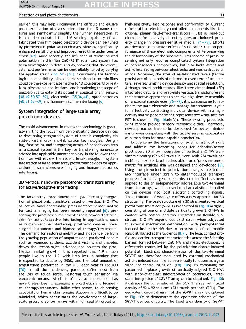
ntegrated circuits and wrap-gate vertical transistor presenthe attractive approaches to achieve high-density assemblyf functional nanodevices [76—79], it is cumbersome to fab-icate the gate electrode and manage interconnect layoutor effectively controlling individual device within a high-ensity matrix (schematic of a representative wrap-gate NWET is shown in Fig. 10a(left)). These existing prosthetickins cannot provide sensory feedback either. Therefore,ew approaches have to be developed for better mimick-ng or even competing with the tactile sensing capabilitiesf human skins for more capable prosthetics.
To overcome the limitations of existing artificial skinsnd address the increasing needs for adaptive/activerostheses, 3D array integration of vertical ZnO NW tran-istors circuitry (92 × 92 taxels in 1 cm2 with 234 taxels pernch) as flexible taxel-addressable force/pressure-sensoratrix for artificial skin was designed and developed [6].sing the piezoelectric polarization charges created at-S interface under strain to gate/modulate transportrocess of local charge carriers, piezotronic effect has beenpplied to design independently addressable two-terminalransistor arrays, which convert mechanical stimuli appliedn the devices into local electronic controlling signals.he elimination of wrap gate offers a new approach for 3Dtructuring. The basic structure of a 3D strain-gated verticaliezotronic transistor (SGVPT) is depicted in Fig. 10a(right),onsisting of one or multiple vertically grown ZnO NWs inontact with bottom and top electrodes on flexible sub-trates. ZnO NW experiences axial strain when subjectedo external mechanical deformation, with piezopotentialnduced inside the NW due to polarization of non-mobileons distributed at the two ends [8,9]. The local contact pro-le and carrier transport characteristics across the Schottkyarrier, formed between ZnO NW and metal electrodes, isffectively controlled by the polarization-charge-inducedotential. Electrical characteristics of the two-terminalGVPT are therefore modulated by external mechanicalctions induced strain, which essentially functions as a gateignal for controlling SGVPT (Fig. 10b). By combining theatterned in-place growth of vertically aligned ZnO NWsith state-of-the-art microfabrication techniques, large-
cale integration of SGVPT array can be obtained. Fig. 10bllustrates the schematic of the SGVPT array with taxel
2014), http://dx.doi.org/10.1016/j.nantod.2013.11.002
ensity of 92 × 92 in 1 cm2 (234 taxels per inch (TPI)). Thequivalent circuit diagram of the SGVPT array is displayedn Fig. 10c to demonstrate the operation scheme of theGVPT devices circuitry. The taxel area density of SGVPT

ARTICLE IN PRESS+ModelNANTOD-344; No. of Pages 24
12 W. Wu et al.
Figure 10 (a) Comparison between three-terminal voltage-gated NW FET (left) and two-terminal strain-gated vertical piezotronictransistor (right). ZnO NWs in SGVPT grow along the c axis, as indicated by the red arrow. (b) Schematic illustration of a 3D SGVPTarray with taxel density of 92 × 92 and scheme for spatial profile imaging of local stress (indicated by the downwards blue arrowhead)by the array (zoom-in schematic). (c) Equivalent circuit diagram of the 3D SGVPT array. The region highlighted by black dashedlines is the unit SGVPT device, in which εg represents the mechanical strain gate signal and the vertical dotted line between thetwo terminals of SGVPT presents the modulation effect of εg on the conducting characteristics of the device. (d) Topological profileimage of the SGVPT array (top view). Inset, 3D perspective view of the topological profile image reveals the vertical hierarchy ofthe SGVPT assembly in which the color gradient represents different heights. (e) Transparency and flexibility of SGVPT array device.( nd, tR an As
atasfaaaoNS(as[a
ettZnrapsaip
For interpretation of the references to color in this figure legeeprinted with permission from [6]. Copyright 2013 the Americ
rray is 8464 cm—2, which is higher than the number ofactile sensors in recent reports (∼6—27 cm—2) [71—73,80]nd mechanoreceptors embedded in the human fingertipkins (∼240 cm—2) [81]. A detailed description of the deviceabrication process is elaborated in Ref [6]. Briefly, thective array of SGVPTs is sandwiched between the topnd bottom Indium Tin Oxide (ITO) electrodes, which areligned in orthogonal cross-bar configurations. A thin layerf Au is deposited between the top/bottom surfaces of ZnOWs and top/bottom ITO electrodes, respectively, formingchottky contacts with ZnO NWs. A thin layer of Parylene C1 �m thickness) is conformally coated on the SGVPT device
Please cite this article in press as: W. Wu, et al., Nano Today (
s the moisture/corrosion barrier. Well-aligned ZnO NWs,ynthesized by a low-temperature hydrothermal method52], function as the active channel material of SGVPTnd help reduce the stochastic taxel-to-taxel variation to
tcle
he reader is referred to the web version of the article.)sociation for the Advancement of Science.
nsure uniform device performance Fig. 10d(inset) showshe SGVPT after etching-back the SU 8 layer and exposingop portions (∼20 �m) of the ZnO NWs. The as-synthesizednO NWs show single-crystallinity. The three-dimensionalature and vertical hierarchy of the SGVPT assembly isevealed by topological profile imaging (Fig. 10d) usingn optical noncontact profilometer, which measures thehase change of light reflected from various heights in thetructure by interferometry. The high degree in alignmentnd uniformity of SGVPT array in three dimensions (∼30 �mn height and 20 �m × 20 �m in taxel size) is enabled byrocess control in both the bottom-up synthesis of NWs and
2014), http://dx.doi.org/10.1016/j.nantod.2013.11.002
op-down fabrication of circuitry. The use of a two-terminalonfiguration based on piezotronic effect simplifies theayout design and circuitry fabrication while maintainsffective control over individual devices. Transparency and

ARTICLE IN PRESS+ModelNANTOD-344; No. of Pages 24
Piezotronics and piezo-phototronics 13
Figure 11 (a) Topological profile images (top view) of 23 selected taxels in a 1 × 92 SGVPT array (single channel) (top frame) andtheir corresponding current responses (middle and bottom frames) under 1 V bias with and without external stress (20 kPa) appliedto certain localized region (around taxels 45 and 46). (b) Single-channel conductance measurement in temporal domain illustratingthe dynamic response of the 23 selected SGVPT devices in this channel, with and without pressure applied. (c) Current responsesfor taxel 46 under different pressures, presenting the gate modulation effect of applied pressure on the electrical characteristicsof SGVPT. Top right inset, current variations (red squares) are plotted versus the applied pressures, clearly showing the saturationof current change when applied pressure is above ∼30 kPa. Bottom left inset, schematic band-diagram illustrating the change inSchottky barrier height of the reversed biased top contact due to the modulation effect of strain-induced piezopotential. Colorgradient represents the distribution of piezopotential field, in which red indicates the positive piezopotential and blue indicatesthe negative piezopotential. The original band-edges at the reversed biased Schottky contact for the SGVPT device without stressapplied are shown in the black solid lines. The band-edges bending at the reversed biased Schottky contact for the SGVPT devicewith stress applied are shown in the blue dashed lines. (For interpretation of the references to color in this figure legend, the reader
an As
(4dp(opc
is referred to the web version of the article.)Reprinted with permission from [6]. Copyright 2013 the Americ
flexibility of SGVPT array devices are also demonstrated(Fig. 10e).
Cross-bar electrodes have been configured for multi-plexed data acquisition and spatial profiles of applied stresscan be imaged. The output signal is current response sothat it is easy to integrate SGVPT array with back-end inter-face circuits for fast data processing. Representative datafrom 23 taxels in a typical single-channel line-scan (1 × 92)
Please cite this article in press as: W. Wu, et al., Nano Today (
measurement is shown in Fig. 11. The corresponding topo-logical profile images (top view) of the selected taxels aredisplayed at the top of Fig. 11a. Current response from eachtaxel under 1 V bias, with and without external pressure
dics
sociation for the Advancement of Science.
20 kPa) applied to a localized region (around taxels 45 and6), is recorded. Dynamic response show distinctive con-uctance changes for taxels before and after applying theressure (Fig. 11b). Although the measured response timerise time) of ∼0.15 s for SGVPT taxel is larger than thatf human fingertips (∼30—50 ms) [6], it is comparable toreviously reported values of 0.1 s [71]. These results indi-ate that SGVPT array can respond to both static and some
2014), http://dx.doi.org/10.1016/j.nantod.2013.11.002
ynamic stimuli. The response time can be further improvedn future design by integrating local on-site signal-processingircuits with SGVPT array [82]. It can be seen that for thisingle-channel array of SGVPTs, pressure variations can be

IN+ModelN
1
dtfrfividcmpafw[atsSTbasarcdttTatbaiotrSt
a3rudrpaweototaosoait
fc
ipsrwassssptalckooett2faTra
adicobtett∼aabbbTbatmSitFiS
ARTICLEANTOD-344; No. of Pages 24
4
istinguished with both high sensitivity and spatial resolu-ion (taxel periodicity ∼100 �m). The dominant mechanismor the transport property of SGVPT is piezotronic effectather than piezoresistive effect, as experimentally con-rmed and elaborated in details [6]. From the measuredariations in current responses by consecutively increas-ng the pressure load applied at fixed location, the SGVPTevice demonstrates high sensitivity for detecting pressurehange, particularly in low-pressure regions (<10 kPa). Theodulation effect of applied pressure is shown from thelot of current variations against pressure changes (Fig. 11c)nd the observed sensing range of a few kPa to ∼30 kPaor SGVPT array is well matched to the 10—40 kPa rangehich a human finger applies to sense texture and shape
83]. The sensitivity for SGVPT, defined as S = dGSGVPT/dP, isround 2.1 �S kPa−1, which arises from the change in carrierransport of the SGVPT by applied pressure due to corre-ponding modulation of barrier height at the reversed biasedchottky contact by strain-induced piezopotential [8,9,28].he conductance of SGVPT device is dictated by the reversediased Schottky contact, which is formed between ZnO NWsnd top electrodes in this case. Upon applying the normaltress, negative piezoelectric polarization charges inducedt the reversed biased top Schottky contact raise the bar-ier height at that contact and hence decrease the transportonductance of the SGVPT taxel. The operation of SGVPTevice is therefore based on barrier-interface-modulationhat enables enhanced sensitivity and efficiency comparedo the channel-modulation operation in conventional FETs.he quality of the Schottky contacts has been characterizeds well [6]. The SBHs and ideality factors of the formed con-acts for devices without extra oxygen plasma treatmentefore depositing the top electrode are 0.419 ± 0.011 eVnd 5.84 ± 1.29 respectively, while the SBHs and ideal-ty factors of the formed contacts for devices with extraxygen plasma treatment before depositing the top elec-rode are found to be 0.575 ± 0.013 eV and 2.17 ± 0.33espectively, indicating that the qualities of as-fabricatedchottky contacts have been improved by the oxygen plasmareatment [44].
The successful fabrication of the 92 × 92-taxel SGVPTrray enables a 15—25-fold increase in number of taxels and00—1000-fold increase in taxel area density compared toecent reports [71—73]. The output current of each individ-al SGVPT taxel is measured and averaged within a shorturation window of 10 ms. By monitoring the output cur-ent of each independently functioning SGVPT taxel, spatialrofile of applied pressure can be imaged by multiplexed-ddressing all of the taxels. Metrology mapping performedithout applying pressure demonstrates good uniformity inlectrical characteristics among all of the taxels, with allf the 8464 SGVPTs within the array functioning and 95% ofhe SGVPTs possessing current values in the narrow rangef 13.7 ± 2.73 �A under 1 V bias (Fig. 12a). Fig. 12b presentshe difference between current values for each taxel beforend after applying the normal stress, confirming that profilef applied stress can be spatially imaged. SGVPT devices aretill operational and capable of imaging the spatial profile
Please cite this article in press as: W. Wu, et al., Nano Today (
f applied pressure after 24-h immersion in 23 ◦C DI waternd 37 ◦C 0.9% saline solution as well as after 6-h immersionn 65 ◦C DI water and 65 ◦C 0.9% saline solution, indicatinghe good stability and feasibility of SGVPT array operation
svtw
PRESSW. Wu et al.
or future applications like in vivo physiological sensing inomplex environments [6].
The device matrix has also been demonstrated for achiev-ng multi-dimensional active sensing, which demonstrate theotential of utilizing SGVPT array for future applicationsuch as multi-dimensional signature recognition by not onlyecording the calligraphy or signature patterns, when peoplerite, but also registering the corresponding pressure/forcepplied at each location/taxel and writing speed by the per-on. Normal stresses with well-determined values as well aspatial locations are applied to the device using the 3-axistage and force gauge. The first group of six normal localtresses, each around 8.1 kPa, are applied to the array atre-programmed locations in the sequence indexed from 1o 6, with the corresponding contours imaged and organized,s shown in Fig. 12c1, to emulate the writing calligraphy ofetter ‘‘A’’ (outlined by the white dashed lines). This pro-ess is achieved by varying the x and y coordinates whileeeping the z coordinate constant in the control interfacef the 3-axis stage. It can be seen that spatial profiles of allf the six applied stresses can be distinguished and mappedlectronically. The second group of six normal stresses withhe same locations are subsequently applied to the array inhe same sequence, except that the stresses applied at sites
and 3 are increased to ∼20 kPa with stresses at the restour sites unchanged. The corresponding mapped contoursre again recorded and organized, as shown in Fig. 12c2.his augmented capability can essentially provide means forealizing personal signature recognition with unique identitynd enhanced security.
The SGVPT array has also shown capability of shape-daptive high-resolution tactile imaging. The real timeetection of shape changes caused by stretching or twistings a desirable feature for sensors embedded in an artifi-ial tissue or prosthetic device. A rectangular supportingbject is fixed to the platen of probe station, directlyeneath the central region of SGVPT array (Fig. 13). Afterhe probe pins are in contact with the pads at the periph-ral of SGVPT devices, the platen is further raised up sohat SGVPT device is hunched by the underneath suppor-ing object (Fig. 13, bottom) with the radius of curvature79.63 mm. The measured difference in taxel currents withnd without the underneath supporting object is mappednd plotted in Fig. 13b1, illustrating a good agreementetween the detected shape change of SGVPT array (darklue regions) and the physical shape of the supporting objecteneath the SGVPT device (outlined by white dashed lines).he shape-adaptive sensing capability is further examinedy applying an additional localized stress to the bent SGVPTrray, using the same setup in Fig. 12, as depicted byhe 3D schematic drawing in Fig. 13b (bottom right). Theeasured variations in taxel current values between bent
GVPT array with extra stress and unstrained SGVPT arrays imaged and plotted in Fig. 13b2. A clearer demonstra-ion of the data can be obtained by numerically subtractingig. 13b1 from Fig. 13b2, which gives rise to spatial imag-ng of the additionally applied stress when the shape of theGVPT device changes (Fig. 13b2—b1). Such shape-adaptive
2014), http://dx.doi.org/10.1016/j.nantod.2013.11.002
ensing has also been investigated for other radii of cur-atures [6]. Because of the relatively large thickness ofhe SGVPT device (mainly contributed by the PET substratehich is 500 �m thick), the saturation of SGVPT response

ARTICLE IN PRESS+ModelNANTOD-344; No. of Pages 24
Piezotronics and piezo-phototronics 15
Figure 12 (a) Metrology mapping (inset) and statistic investigation of the fully integrated SGVPT array without applying stress.(b) Current responses contour plot illustrating the capability of SGVPT array for imaging the spatial profile of applied stress. Colorbar represents the current differences for each taxel before and after applying the normal stress. The physical shape of the appliedstress is highlighted by the white dashed lines. (c) Multi-dimensional sensing by SGVPT array exhibits the potential of realizingapplications like personal signature recognition with maximum security and unique identity. The calligraphy of written letter ‘‘A’’
an As
1a
pstoaaaa3stt
is highlighted by the white dashed lines.Reprinted with permission from [6]. Copyright 2013 the Americ
under large pressure (as shown in Fig. 11c) and the con-straints of measurement set up (probes on probe card havelimited movement in vertical direction), the SGVPT arrayis unable to sense the change in device shape and furtherdistinguish the applied pressure when radii of curvature issmaller than 30—35 mm (Fig. 13c). The detectable range ofshape deformation as well as corresponding shape-adaptivesensing can be improved by engineering the device into morecompliant form to reduce the strain induced in SGVPT dueto change in device shape. Cyclic bending has been furtherperformed on SGVPT array for investigating the reliabilityand stability of device operations. In order to acceleratethe aging process, SGVPT array has been repeatedly bent toa very small radius of curvature (15 mm) with 2-Hz cyclefrequency. Metrology mapping has then been performed
Please cite this article in press as: W. Wu, et al., Nano Today (
on SGVPT array and plotted for comparison with that ofdevice before the cyclic bending. No significant degrada-tion can be observed in operation of SGVPT array even after
aai
sociation for the Advancement of Science.
000-cycle bending, suggesting good stability in device oper-tion.
Moreover, the SGVPT devices can also function as self-owered active tactile sensors by converting mechanicaltimulations into electrical signals utilizing the piezopoten-ial without applied bias, which emulates the physiologicalperations of mechanoreceptors in biological entities, suchs human hair follicles and hair cells in the cochlea. Thebove technology is the first instance demonstrating 3Drray integration of vertical NW piezotronic transistors forctive/adaptive tactile imaging. It is also by far the largestD array integration of functional nanomaterials for artificialkin by combining the bottom-up synthesis of nanoma-erials with state-of-art top-down micro-fabrications. Theechnology of 3D piezotronic transistor array offers immedi-
2014), http://dx.doi.org/10.1016/j.nantod.2013.11.002
te opportunities to meet needs from research, consumernd clinical sectors (e.g. in the fast-growing prosthet-cs market). The SGVPT array based technology for the

ARTICLE IN PRESS+ModelNANTOD-344; No. of Pages 24
16 W. Wu et al.
Figure 13 (a) Optical photographs of the experimental setup for investigating the feasibility of SGVPT array for shape-adaptivesensing. The top one is the top view of the setup. The bottom one is the side-view of the setup, with the device deformed. (b)Shape-adaptive sensing of the SGVPT array. (b1) The measured difference in taxel currents for SGVPT array with and withoutunderneath supporting object. The detected shape change of SGVPT array is illustrated by the dark blue regions and the physicalshape of the supporting object beneath the SGVPT device is outlined by the white dashed lines. (b2) The measured variations intaxel current values between bent SGVPT array with extra stress and unstrained SGVPT array. The location/shape of the extra stressis outlined by the red dashed lines. (b2—b1) A clearer demonstration of the data is obtained by numerically subtracting Fig. 4b1from Fig. 4b2, giving rise to spatial imaging of the additionally applied stress when the shape of the SGVPT device is changed. The3D schematic drawing at the bottom right illustrates the process for shape-adaptive sensing. (c) Experimental results showing thelimit for shape-adaptable sensing by SGVPT array with current design. (For interpretation of the references to color in this figurel .)R an As
fittauwii
Pi
Ttoe
tesfodmiisd
g
egend, the reader is referred to the web version of the articleeprinted with permission from [6]. Copyright 2013 the Americ
rst time allows us to directly control large-scale func-ional electronics by mechanical stimulations and enableshe active/adaptive interfacing between electronics andmbient. These capabilities emerge directly from theniqueness of the technology in ways that are impossibleith existing approaches. It also exhibits the potential to be
ntegrated with silicon-based CMOS technology and hencets potential and impact is broad.
iezoelectric NW LED array for electroluminescentmaging of pressure distribution
Please cite this article in press as: W. Wu, et al., Nano Today (
he piezoelectric polarization charges can also tune/controlhe charge separation, transport and/or recombination inptoelectronic processes [9,25,8], which has been used tonhance the performance of photocells [63,66,69,84—86],
ipLw
sociation for the Advancement of Science.
he sensitivity of photodetectors [87—90] and the externalfficiency of an LED [64,67]. It has been recently demon-trated that strain-controlled LED emission can be used toabricate a rapidly responding, optically based pixel arrayf strain sensors to directly ‘image’ the force/pressureistribution on the device at a resolution of only a fewicrometers [91]. The design principle makes use of strain-
nduced polarization charges to tune the local light-emittingntensity of individual NW-LEDs. The two-dimensional inten-ity distribution then becomes a map of the pressureistribution on the surface.
The device was based on a patterned array of n-ZnO NWsrown on a p-GaN thin-film substrate, with the c-axis point-
2014), http://dx.doi.org/10.1016/j.nantod.2013.11.002
ng upwards from the film (Fig. 14a) [52], forming an array ofixelled light emitters. Details about the fabrication of thisED array device can be found in Ref. [91]. Briefly, The NWsere fabricated by combining photolithography patterning

ARTICLE IN PRESS+ModelNANTOD-344; No. of Pages 24
Piezotronics and piezo-phototronics 17
Figure 14 (a) Design of the NW-LED-based pressure sensor array before applying a compressive strain. Insets: top, SEM images ofthe as-grown ZnO NW arrays on the p-GaN film; bottom: an ITO layer is deposited as a common electrode on top of the n-ZnO NWs.(b) Optical image of a NW-LED array when electrically emitting light. Insets: Five typical NW LEDs (marked with a red rectangle ina) and a corresponding line profile of the emission intensity from which the possible spatial resolution achieved by the sensor canbe estimated. (c) Corresponding optical spectra of emitted light at bias voltages of 6, 7, 8, 9 and 10 V. Inset: dependence of peakposition on applied voltage. (d) Optical image of a fabricated device and corresponding image when the device was electrically litup at a bias voltage of 5 V, showing blue-white light emission from the NW-LED array. Scale bar is 5 mm. (For interpretation of the
to thblish
rmtrcaTvftdb
oc
references to color in this figure legend, the reader is referred
Reprinted with permission from [91]. Copyright 2013 Nature Pu
and low-temperature wet chemical growth. Ordered arraysof vertical n-type ZnO NWs were fabricated by uniform epi-taxial growth on a p-GaN film to form the basic pixels ofthe sensors (Fig. 14a, inset). Scanning electron microscopy(SEM) images clearly show that all the NWs are wrappedby PMMA, and that the heads of the nanowires are exposedfollowing oxygen plasma etching (Fig. 14a, inset). A Ni/Auelectrode was used to form Ohmic contact with the bot-tom p-GaN, and an ITO layer was deposited in direct contactwith the ZnO NWs on top, thereby serving as common elec-trodes for the entire NW array. The NW-LED array can beuniformly lit up under a bias of 5 V. An optical image of alit LED array is shown in Fig. 14b, where each MW is a sin-gle light emitter and also a pixel unit. The center-to-centerdistance between two adjacent spots is 4 �m, correspond-
Please cite this article in press as: W. Wu, et al., Nano Today (
ing to a pixel resolution of 6350 dpi. Five typical NW-LEDsmarked with a red rectangle in Fig. 14b are enlarged anddisplayed together with their intensity line profile. Thereis little crosstalk between adjacent pixels, and the actual
osea
e web version of the article.)ing Group.
esolution is 2.7 �m, as defined by the full-width at halfaximum (FWHM) of the emission pixels. The emission spec-
ra obtained at different bias voltages (6, 7, 8, 9, 10 V) atoom temperature are shown in Fig. 14c. Electrolumines-ence intensity increases with an increase in bias voltage,s expected from the band-bending model of a p—n junction.he major emission peak located at 406 nm is identified asiolet-blue emission, which can be associated with the inter-ace emission [92] and does not show any obvious shift whenhe bias voltage is increased. Corresponding image when theevice was electrically lit up at a bias voltage of 5 V showslue-white light emission from the NW-LED array (Fig. 14d).
Straining the basic unit cell of ZnO results in polarizationf the cations and anions in the crystal because of its non-entrally symmetric structure. A schematic band diagram
2014), http://dx.doi.org/10.1016/j.nantod.2013.11.002
f a p-GaN/n-ZnO p—n junction composed of NW-LEDs, ashown in Fig. 15a, can be used to illustrate the piezotronicffect on the device before (black line) and after (red line)pplying a strain. When the ZnO NW is under compressive

ARTICLE IN PRESS+ModelNANTOD-344; No. of Pages 24
18 W. Wu et al.
Figure 15 (a) Schematic band diagram of a p-GaN/n-ZnO p—n junction before (black line) and after (red line) applying a com-pressive strain, where the dip created at the interface is due to the non-mobile, positive ionic charges. (b) Fast response andrecovery of the NW-LED pressure sensors. Inset: enlarged image of one cycle, showing response and recovery times of ∼90 ms. (c)Enhancement factor E of a NW-LED as a function of an applied compressive strain of up to −0.15%, together with the correspondingemitting light images. (For interpretation of the references to color in this figure legend, the reader is referred to the web versionoR blish
sitpNtrtzptiFNa
tlcptttpatpl
f the article.)eprinted with permission from [91]. Copyright 2013 Nature Pu
train, the strain inside the NW is much larger than thatn the GaN film because of the low coverage of NWs onhe substrate surface (small contact cross-section), so aiezopotential is created in the NW. If the c-axis of the ZnOWs is pointing away from the GaN film, the presence ofhe non-mobile, positive ionic charges at the p—n junctionegion may result in a local dip in the band if the concen-ration of free carriers is low within the charge-depletionone of the junction. The distorted band tends to tem-orarily trap holes near the GaN—ZnO interface, increasinghe carrier injection rates toward the junction region, andncreasing the recombination rate of electrons and holes.
Please cite this article in press as: W. Wu, et al., Nano Today (
urthermore, the presence of the piezopotential along theW is equivalent to applying an extra forward-biased volt-ge on the device. The depletion width and internal field are
ini
ing Group.
herefore reduced, and the injection current and emittingight intensity subsequently increased, when the device isompressed [8,9,12]. The results are supported by a theoryroposed in relation to the photon emission at a p—n junc-ion in the presence of local piezoelectric charges. In thisheoretical work, analytical results under simplified condi-ions are presented with the aim of understanding the corehysics of the piezotronic devices, and numerical modelsre developed to illustrate the photon emission process andhe carrier transport characteristics of a practical exam-le of the piezoelectric LED [93]. Under forward bias, theight emitting intensity of the NWs under compressive strain
2014), http://dx.doi.org/10.1016/j.nantod.2013.11.002
s increased significantly, while the remaining NWs undero strain show barely any change in electroluminescencentensity. Based on the intensity change of the emitting

IN+Model
−pml(toar
uc[eadtsTmtpftrzooitaisufZdanacaogpdq
osslgahsot
ARTICLENANTOD-344; No. of Pages 24
Piezotronics and piezo-phototronics
nano-LEDs, the pressure/strain distribution across the entirearray can be mapped at a resolution of a few micrometers.This is the principle of our sensor array.
The NW-LED pressure sensor has a fast response and fastrecovery. Fig. 15b shows current versus time for five cyclesof applied pressure. Response an relaxation times of lessthan 0.1 s were measured, which was largely determined bythe period of time needed to apply/retract the mechanicalforce. Indeed, the true response of our device is expectedto be much faster than 0.1 s. The emission intensity of asingle-pixel NW-LED can be largely tuned/controlled by themagnitude of the applied strain. An image taken by a charge-coupled device (CCD) at zero applied strain is taken as thebackground signal, denoted Io. An image of the LEDs takenunder strain ε is denoted Iε. Fig. 15c shows enhancementfactor E of a single representative NW-LED (E = (Iε − Io)/Io)as a function of applied strain up to ε = −0.15%. E is approx-imately linearly dependent on strain, and reaches 300% ata strain of −0.15%, in agreement with theoretical results aslong as the deformation of the ZnO nanowire is limited tothe elastic range. The sensor sensitivity S in terms of rel-ative light intensity enhancement as a function of appliedpressure could be defined as [71]
S = �I/I
�= �I/I
140(GPa)|ε| = E
140|ε| GPa−1
where E is the enhancement factor, � the applied pressure,ε the strain in ZnO NWs and 140 GPa is the Young’s mod-ulus for ZnO NWs. The sensitivity S is hence found to be∼12.88 GPa−1.
The two-dimensional mapping of strain was demon-strated using a convex character pattern of ‘PIEZO’ moldedon a sapphire substrate, which was directly applied onto theLED arrays as a seal (Fig. 16a). Fig. 16b presents an opticalimage of the device with an SU-8 convex mound on top. Eachblack dot is a pixel comprising a single ZnO NW-LED with4 �m pitch. Light-emitting images of the device at appliedstrains of 0, −0.06% and −0.15% were recorded by a CCD,as shown in Fig. 16c—e, respectively. The images unambigu-ously show that the change in LED intensity occurred at thepixels that were being compressed by the molded pattern,while those not affected by the molded characters showedalmost no change in LED intensity. There was little crosstalkbetween adjacent pixels in the device. The spatial strain dis-tribution can be extracted from the LED intensity images. Bycarefully aligning the two images in Fig. 16c and e, an imagefor the enhancement factor E(x, y) = [Iε(x, y) − Io(x, y)]/Io(x,y) was obtained in Fig. 16f, where (x,y) are the coordinatesof the CCD pixels in the plane. The E image provides a spa-tial mapping of pressure applied to the entire array, andclearly shows the word ‘PIEZO’, originating from the mold.The color code indicates that the average enhancement fac-tor E is ∼200%. The signal-to-noise ratio of the E factor canbe derived using the line profile data, as indicated for twopositions in Fig. 16e — one on the molded pattern (verticalpink line) and the other off the pattern (horizontal red line).
Please cite this article in press as: W. Wu, et al., Nano Today (
The results are presented in Fig. 16g and h, respectively.The crosstalk is completely negligible. The E factor for theseven NW-LED pixels on the mold increased by a factor of4—5 (up to 750%) when the applied strain increased from
cZcf
PRESS19
0.06% to −0.15% (Fig. 16g). In contrast, the 36 NW-LEDixels that were off the mold pattern showed no enhance-ent at all, instead having a random variation at the noise
evel when the strain was increased from −0.06% to −0.15%Fig. 16h). This unambiguously shows the gigantic effect ofhe piezoelectricity on LED emission. It proves the principlef using the piezotronic effect for mapping pressure/straint high spatial resolution, with high sensitivity and even higheliability.
The piezoelectric NW-LED-based approach offers a fewnique advantages for imaging strain distribution. First, inontrast to other approaches such as cross-bar electrodes71,72,74], where the pixels are the matrix defined by thelectrodes so that the signal is measured and recorded in
sequential scanning mode, our pixels are defined by theistribution of NWs on the substrate, all of which sharewo common electrodes. In this way, mapping is carried outimultaneously for all pixels at a time resolution of ∼90 ms.he above parallel detection technology offers a much fasterapping rate for creating pressure distribution maps, and
he time resolution is almost dictated by the relaxationrocess in applying/retracting the strain. Furthermore, ourabrication procedure could be simpler and cheaper than forhe cross-bar electrode arrangement. Second, the spatialesolution is much higher and can be improved by optimi-ing the size and distribution of nanowires. The diameterf our nanowires was ∼1.5 �m, the estimated resolution forur devices is given by R(�m) = D + 1.2(�m), where D (�m)s the diameter of the NWs. If the diameter were reducedo 100 nm, we could obtain a resolution of 1.3 �m. Third,lthough our current study is based on a hard substrate, its possible to extend the current approach to a soft sub-trate by directly cutting the current device into smallernits and then transferring these onto a soft substrate toollow a certain pattern. Alternatively, we could fabricatenO p—n homojunction arrays on any substrate (such as poly-imethylsiloxane (PDMS) or fiber). Finally, although therere some variations in the lighting intensity in differentanowires before strain is applied, possibly due to fluctu-tions in junction quality, such ‘background’ informationan be removed using a signal-processing technique, suchs defining an enhancement factor with a relative changef NW intensity before and after straining. Furthermore,rowing high-quality NWs using high-temperature vaporhase techniques, such as metal-organic chemical vaporeposition (MOCVD), may also help to improve mappinguality.
The above approach is scientifically new because it reliesn the piezoelectric polarization charges for designing atable, fast response, as well as parallel-detection strain-ensor arrays. The output signal is electroluminescenceight, which is easy to integrate with photonic technolo-ies for fast data transmission, processing and recording,nd may enable the development of highly intelligentuman-machine interfaces. This may represent a majortep toward on-chip recording of mechanical signals byptical means, with potential applications in touchpadechnology, personalized signatures, bio-imaging and opti-
2014), http://dx.doi.org/10.1016/j.nantod.2013.11.002
al MEMS. Furthermore, with the feasibility of fabricatingnO nanowires on flexible substrates, the current approachould be extended to smart skin, which will have a greatuture in biological sciences, human—machine interfacing,

ARTICLE IN PRESS+ModelNANTOD-344; No. of Pages 24
20 W. Wu et al.
Figure 16 (a) Illustration showing the working process of pressure distribution imaging. (b) Optical image of the device with aconvex mold on top. (c—e) Electroluminescence images of the device at strains of 0, −0.06% and −0.15%, respectively. The imagesclearly show that a change in LED intensity occurred at the pixels that were compressed, while those away from the molded patternshowed almost no change. (f) Two-dimensional contour map of the E(x,y) factor derived from the LED intensity images shown in (c)and (e). It directly presents the word ‘PIEZO’, as given on the mold. (g and h) Line profile data showing the signal-to noise ratio ofthe E factor for two typical positions-one on the molded pattern (vertical pink line, g) and one off the pattern (horizontal red line,( e reftR blish
st
A
Ptaretogmde[a
otsta
pptpestcI
h) showing unambiguous differences. (For interpretation of thhe web version of the article.)eprinted with permission from [91]. Copyright 2013 Nature Pu
mart sensor and processor systems, and even defenseechnology.
pplication prospects
iezoelectric semiconductors has been widely utilized inhe GaN/AlGaN high electron mobility transistors (HEMTs)nd similar effect of piezoelectric polarization on car-ier properties, such as formation of two-dimensionallectron gas (2DEG) with extremely high carrier concentra-ion at the heterojunction interface, has been previouslybserved in HEMT device [94—96]. Theoretical investi-ation also reveals that appreciable piezoelectric fielday be induced inside the nanowire heterostructures
Please cite this article in press as: W. Wu, et al., Nano Today (
ue to lattice mismatch, which can introduce significantffects on the charge carrier transport and confinement86,97]. These piezoelectric fields, whereas, are fixeds introduced by interface strain and remain unchanged
sput
erences to color in this figure legend, the reader is referred to
ing Group.
nce the heterojunction devices are fabricated. In con-rast, the mechanical flexibility of piezoelectric compoundtructures on soft substrates enables more versatile utiliza-ion of piezotronic effect in semiconductors for functionalpplications.
The essence of the emerging research and applications iniezotronics relies on the coupling between strain-inducedolarization and semiconductor properties in piezoelec-ric semiconductor materials. Fundamental research ofiezotronics as well as applications utilizing piezotronicffect introduce new concepts/understandings to classicemiconductor physics by taking into account the con-ributions from piezoelectric polarization to the chargearrier distribution and band structure adjustment (Fig. 17).n addition to the electronics and sensing applications
2014), http://dx.doi.org/10.1016/j.nantod.2013.11.002
hown here in this review, the presence of localizediezoelectric polarization charges can significantly mod-late/control the charge carrier generation, separation,ransport and/or recombination at an interface/junction

ARTICLE IN PRESS+ModelNANTOD-344; No. of Pages 24
Piezotronics and piezo-phototronics 21
zing
for im othe
hn
A
TncpHW
R
Figure 17 Schematic diagram showing the prospects of utiliducting properties of piezoelectric semiconductor materials,
optoelectronics, spintronics, artificial photosynthesis and many
in optoelectronic processes [8,9,67,98,99]. The strain-induced electric fields have been demonstrated to besufficiently large to impose a significant change in theconfined energy states of strained-layer quantum wells[100—102], which may enable novel piezotronic devicesbased on heterogeneous nanostructures (e.g. core/shellor axial p—n junctions). Interfacial strain-induced polar-ization charges can also assist the catalytic process andmodulate the electrochemical activity of related materialsby adjusting the difference between the electrochemi-cal potentials in the systems, which could give rise topiezo-enhanced catalysis or photosynthesis [103—106]. Con-trollable modulation of M-S contact or p—n junction bystrain-induced polarization offers unprecedented method inaddition to the conventional electrical controlling for imple-menting novel electronics, optoelectronics or even spininjection/transport in spintronics applications [107—110]which possess tunable operation characteristics adaptiveto the ambient these devices are deployed. Piezotronicsenables the novel approach for modulating device charac-teristics by tuning the junction/contact properties, whichhas been unavailable in conventional technologies withoutmodifying the interface structure or chemistry. We havedemonstrated here the advances from single piezotronic
Please cite this article in press as: W. Wu, et al., Nano Today (
nanodevices to an array of devices and eventually to an inte-grated functional piezotronic system, which is a landmarkprogress in the field of nanotechnology. It is prospected thatpiezotronics will enable technology advances in sensing,
piezotronic effect, which couples piezoelectric and semicon-plementing many novel applications in tunable electronics,
r areas.
uman—electronics interfacing, robotics, biomedical diag-osis/therapy and prosthetics.
cknowledgements
he authors thank the support of NSF, DARPA, NIH and Chi-ese Academy of Sciences. We sincerely thank the followingolleagues who made significant contributions to the workresented here: (not in particular order): Jun Zhou, Youfanu, Xudong Wang, Qing Yang, Ying Liu, Jr-Hau He, Yifan Gao,eihua Han, Yusheng Zhou, Simiao Niu and many others.
eferences
[1] H.C. Ko, M.P. Stoykovich, J.Z. Song, V. Malyarchuk, W.M. Choi,C.J. Yu, J.B. Geddes, J.L. Xiao, S.D. Wang, Y.G. Huang, J.A.Rogers, Nature 454 (2008) 748—753.
[2] B.Z. Tian, J. Liu, T. Dvir, L.H. Jin, J.H. Tsui, Q. Qing, Z.G. Suo,R. Langer, D.S. Kohane, C.M. Lieber, Nat. Mater. 11 (2012)986—994.
[3] C. Wang, D. Hwang, Z. Yu, K. Takei, J. Park, T. Chen, B. Ma,A. Javey, Nat. Mater. 12 (2013) 899—904.
[4] C. Keplinger, J.-Y. Sun, C.C. Foo, P. Rothemund, G.M. White-sides, Z. Suo, Science 341 (2013) 984—987.
2014), http://dx.doi.org/10.1016/j.nantod.2013.11.002
[5] T. Dvir, B.P. Timko, M.D. Brigham, S.R. Naik, S.S. Karajanagi,O. Levy, H.W. Jin, K.K. Parker, R. Langer, D.S. Kohane, Nat.Nanotechnol. 6 (2011) 720—725.
[6] W.Z. Wu, X.N. Wen, Z.L. Wang, Science 340 (2013) 952—957.

IN+ModelN
2
ARTICLEANTOD-344; No. of Pages 24
2
[7] A.P. Alivisatos, A.M. Andrews, E.S. Boyden, M. Chun,G.M. Church, K. Deisseroth, J.P. Donoghue, S.E. Fraser, J.Lippincott-Schwartz, L.L. Looger, S. Masmanidis, P.L. McEuen,A.V. Nurmikko, H. Park, D.S. Peterka, C. Reid, M.L. Roukes, A.Scherer, M. Schnitzer, T.J. Sejnowski, K.L. Shepard, D. Tsao,G. Turrigiano, P.S. Weiss, C. Xu, R. Yuste, X.W. Zhuang, ACSNano 7 (2013) 1850—1866.
[8] Z.L. Wang, Adv. Mater. 24 (2012) 4632—4646.[9] Z.L. Wang, Piezotronics and Piezo-Phototronics, Springer,
Berlin, Heidelberg, 2013.[10] Z.L. Wang, W.Z. Wu, Angew. Chem. Int. Ed. 51 (2012)
11700—11721.[11] G. Gautschi, Piezoelectric Sensorics: Force, Strain, Pressure,
Acceleration and Acoustic Emission Sensors, Materials andAmplifiers, Springer, Berlin, Heidelberg, 2002.
[12] Z.L. Wang, Nano Today 5 (2010) 540—552.[13] Z.L. Wang, Adv. Mater. 19 (2007) 889—892.[14] X.D. Wang, J. Zhou, J.H. Song, J. Liu, N.S. Xu, Z.L. Wang,
Nano Lett. 6 (2006) 2768—2772.[15] Z.Y. Gao, J. Zhou, Y.D. Gu, P. Fei, Y. Hao, G. Bao, Z.L. Wang,
J. Appl. Phys. 105 (2009) 113707.[16] L. Schmidt-Mende, J.L. MacManus-Driscoll, Mater. Today 10
(2007) 40—48.[17] Y. Gao, Z.L. Wang, Nano Lett. 9 (2009) 1103—1110.[18] Z.L. Wang, J.H. Song, Science 312 (2006) 242—246.[19] D.J. Bayerl, X.D. Wang, Adv. Funct. Mater. 22 (2012)
652—660.[20] M.P. Lu, J. Song, M.Y. Lu, M.T. Chen, Y. Gao, L.J. Chen, Z.L.
Wang, Nano Lett. 9 (2009) 1223—1227.[21] G.D. Yuan, W.J. Zhang, J.S. Jie, X. Fan, J.A. Zapien, Y.H.
Leung, L.B. Luo, P.F. Wang, C.S. Lee, S.T. Lee, Nano Lett. 8(2008) 2591—2597.
[22] F. Wang, J.H. Seo, D. Bayerl, J.A. Shi, H.Y. Mi, Z.Q. Ma, D.Y.Zhao, Y.C. Shuai, W.D. Zhou, X.D. Wang, Nanotechnology 22(2011) 225602.
[23] K.C. Pradel, W.Z. Wu, Y.S. Zhou, X.N. Wen, Y. Ding, Z.L. Wang,Nano Lett. 13 (2013) 2647—2653.
[24] A.B. Yankovich, B. Puchala, F. Wang, J.H. Seo, D. Morgan, X.D.Wang, Z.Q. Ma, A.V. Kvit, P.M. Voyles, Nano Lett. 12 (2012)1311—1316.
[25] Z.L. Wang, MRS Bull. 37 (2012) 814—827.[26] X.D. Wang, Am. Ceram. Soc. Bull. 92 (2013) 18—23.[27] J. Shi, M.B. Starr, X.D. Wang, Adv. Mater. 24 (2012)
4683—4691.[28] Y. Zhang, Y. Liu, Z.L. Wang, Adv. Mater. 23 (2011) 3004—3013.[29] H.D. Espinosa, R.A. Bernal, M. Minary-Jolandan, Adv. Mater.
24 (2012) 4656—4675.[30] R.T. Tung, Mater. Sci. Eng. R 35 (2001) 1—138.[31] E.H. Rhoderick, R.H. Williams, Metal—Semiconductor Con-
tacts, 2nd ed., Clarendon Press, Oxford, 1988.[32] L.J. Brillson, Y.C. Lu, J. Appl. Phys. 109 (2011) 121301.[33] Z.L. Wang, Adv. Mater. 24 (2012) 4630—4631.[34] C.R. Crowell, S.M. Sze, Solid State Electron. 9 (1966)
1035.[35] W.Z. Wu, Y.G. Wei, Z.L. Wang, Adv. Mater. 22 (2010) 4711.[36] W.H. Han, Y.S. Zhou, Y. Zhang, C.Y. Chen, L. Lin, X. Wang,
S.H. Wang, Z.L. Wang, ACS Nano 6 (2012) 3760—3766.[37] R.S. Muller, T.I. Kamins, M. Chan, Device Electronics for Inte-
grated Circuits, 3rd ed., John Wiley & Sons, Inc., New York,NY, 2003.
[38] J. Zhou, Y.D. Gu, P. Fei, W.J. Mai, Y.F. Gao, R.S. Yang, G. Bao,Z.L. Wang, Nano Lett. 8 (2008) 3035—3040.
[39] J. Zhou, P. Fei, Y.D. Gu, W.J. Mai, Y.F. Gao, R. Yang, G. Bao,Z.L. Wang, Nano Lett. 8 (2008) 3973—3977.
Please cite this article in press as: W. Wu, et al., Nano Today (
[40] P. Fei, P.H. Yeh, J. Zhou, S. Xu, Y.F. Gao, J.H. Song, Y.D. Gu,Y.Y. Huang, Z.L. Wang, Nano Lett. 9 (2009) 3435—3439.
PRESSW. Wu et al.
[41] Y.S. Zhou, K. Wang, W.H. Han, S.C. Rai, Y. Zhang, Y. Ding,C.F. Pan, F. Zhang, W.L. Zhou, Z.L. Wang, ACS Nano 6 (2012)6478—6482.
[42] W.H. Liu, M. Lee, L. Ding, J. Liu, Z.L. Wang, Nano Lett. 10(2010) 3084—3089.
[43] R.M. Yu, W.Z. Wu, Y. Ding, Z.L. Wang, ACS Nano 7 (2013)6403—6409.
[44] W.Z. Wu, Z.L. Wang, Nano Lett. 11 (2011) 2779—2785.[45] J. Zhou, Y.D. Gu, Y.F. Hu, W.J. Mai, P.H. Yeh, G. Bao,
A.K. Sood, D.L. Polla, Z.L. Wang, Appl. Phys. Lett. 94(2009) 191103.
[46] P.H. Yeh, Z. Li, Z.L. Wang, Adv. Mater. 21 (2009) 4975—4978.[47] T.Y. Wei, P.H. Yeh, S.Y. Lu, Z. Lin-Wang, J. Am. Chem. Soc.
131 (2009) 17690—17695.[48] R. Yu, C. Pan, J. Chen, G. Zhu, Z.L. Wang, Adv. Funct. Mater.
23 (2013) 5868—5874.[49] C.F. Pan, R.M. Yu, S.M. Niu, G. Zhu, Z.L. Wang, ACS Nano 7
(2013) 1803—1810.[50] R.M. Yu, C.F. Pan, Z.L. Wang, Energ. Environ. Sci. 6 (2013)
494—499.[51] S. Niu, Y. Hu, X. Wen, Y. Zhou, F. Zhang, L. Lin, S. Wang, Z.L.
Wang, Adv. Mater. 25 (2013) 3701—3706.[52] Y.G. Wei, W.Z. Wu, R. Guo, D.J. Yuan, S.M. Das, Z.L. Wang,
Nano Lett. 10 (2010) 3414—3419.[53] Y. Huang, X.F. Duan, Q.Q. Wei, C.M. Lieber, Science 291 (2001)
630—633.[54] J. Wallentin, N. Anttu, D. Asoli, M. Huffman, I. Aberg, M.H.
Magnusson, G. Siefer, P. Fuss-Kailuweit, F. Dimroth, B. Witzig-mann, H.Q. Xu, L. Samuelson, K. Deppert, M.T. Borgstrom,Science 339 (2013) 1057—1060.
[55] D.J. Yuan, R. Guo, Y.G. Wei, W.Z. Wu, Y. Ding, Z.L. Wang, S.M.Das, Adv. Funct. Mater. 20 (2010) 3484—3489.
[56] X.N. Wen, W.Z. Wu, Y. Ding, Z.L. Wang, J. Mater. Chem. 22(2012) 9469—9476.
[57] Y.S. Zhou, R. Hinchet, Y. Yang, G. Ardila, R. Songmuang, F.Zhang, Y. Zhang, W.H. Han, K. Pradel, L. Montes, M. Mouis,Z.L. Wang, Adv. Mater. 25 (2013) 883—888.
[58] R.M. Yu, L. Dong, C.F. Pan, S.M. Niu, H.F. Liu, W. Liu, S. Chua,D.Z. Chi, Z.L. Wang, Adv. Mater. 24 (2012) 3532—3537.
[59] J.M. Wu, C.Y. Chen, Y. Zhang, K.H. Chen, Y. Yang, Y.F. Hu, J.H.He, Z.L. Wang, ACS Nano 6 (2012) 4369—4374.
[60] L. Dong, S.M. Niu, C.F. Pan, R.M. Yu, Y. Zhang, Z.L. Wang, Adv.Mater. 24 (2012) 5470—5475.
[61] Y.F. Hu, Y. Zhang, L. Lin, Y. Ding, G. Zhu, Z.L. Wang, NanoLett. 12 (2012) 3851—3856.
[62] X.N. Wen, W.Z. Wu, Y. Ding, Z.L. Wang, Adv. Mater. 25 (2013)3371—3379.
[63] X.N. Wen, W.Z. Wu, Z.L. Wang, Nano Energy 2 (2013)1093—1100.
[64] Q. Yang, Y. Liu, C.F. Pan, J. Chen, X.N. Wen, Z.L. Wang, NanoLett. 13 (2013) 607—613.
[65] F. Zhang, Y. Ding, Y. Zhang, X.L. Zhang, Z.L. Wang, ACS Nano6 (2012) 9229—9236.
[66] C.F. Pan, S.M. Niu, Y. Ding, L. Dong, R.M. Yu, Y. Liu, G. Zhu,Z.L. Wang, Nano Lett. 12 (2012) 3302—3307.
[67] Q. Yang, W.H. Wang, S. Xu, Z.L. Wang, Nano Lett. 11 (2011)4012—4017.
[68] Q. Yang, X. Guo, W.H. Wang, Y. Zhang, S. Xu, D.H. Lien, Z.L.Wang, ACS Nano 4 (2010) 6285—6291.
[69] Y.F. Hu, Y. Zhang, Y.L. Chang, R.L. Snyder, Z.L. Wang, ACSNano 4 (2010) 4220—4224.
[70] K. Ziegler-Graham, E.J. MacKenzie, P.L. Ephraim, T.G. Trav-ison, R. Brookmeyer, Arch. Phys. Med. Rehabil. 89 (2008)422—429.
2014), http://dx.doi.org/10.1016/j.nantod.2013.11.002
[71] K. Takei, T. Takahashi, J.C. Ho, H. Ko, A.G. Gillies, P.W. Leu,R.S. Fearing, A. Javey, Nat. Mater. 9 (2010) 821—826.

IN+Model
[
[
[[
[
[
[
fvI2aaop
i(nf
ARTICLENANTOD-344; No. of Pages 24
Piezotronics and piezo-phototronics
[72] S.C.B. Mannsfeld, B.C.K. Tee, R.M. Stoltenberg, C.V.H.H.Chen, S. Barman, B.V.O. Muir, A.N. Sokolov, C. Reese, Z.N.Bao, Nat. Mater. 9 (2010) 859—864.
[73] T. Someya, T. Sekitani, S. Iba, Y. Kato, H. Kawaguchi, T. Saku-rai, Proc. Natl. Acad. Sci. U.S.A. 101 (2004) 9966—9970.
[74] D.J. Lipomi, M. Vosgueritchian, B.C.K. Tee, S.L. Hellstrom,J.A. Lee, C.H. Fox, Z.N. Bao, Nat. Nanotechnol. 6 (2011)788—792.
[75] D.H. Kim, N.S. Lu, R. Ma, Y.S. Kim, R.H. Kim, S.D. Wang, J. Wu,S.M. Won, H. Tao, A. Islam, K.J. Yu, T.I. Kim, R. Chowdhury,M. Ying, L.Z. Xu, M. Li, H.J. Chung, H. Keum, M. McCormick,P. Liu, Y.W. Zhang, F.G. Omenetto, Y.G. Huang, T. Coleman,J.A. Rogers, Science 333 (2011) 838—843.
[76] A. Javey, S. Nam, R.S. Friedman, H. Yan, C.M. Lieber, NanoLett. 7 (2007) 773—777.
[77] J.H. Ahn, H.S. Kim, K.J. Lee, S. Jeon, S.J. Kang, Y.G. Sun,R.G. Nuzzo, J.A. Rogers, Science 314 (2006) 1754—1757.
[78] S. Nam, X.C. Jiang, Q.H. Xiong, D. Ham, C.M. Lieber, Proc.Natl. Acad. Sci. U.S.A. 106 (2009) 21035—21038.
[79] T. Bryllert, L.E. Wernersson, L.E. Froberg, L. Samuelson, IEEEElectron. Device Lett. 27 (2006) 323—325.
[80] T. Sekitani, T. Yokota, U. Zschieschang, H. Klauk, S. Bauer,K. Takeuchi, M. Takamiya, T. Sakurai, T. Someya, Science 326(2009) 1516—1519.
[81] R.S. Johansson, A.B. Vallbo, J. Physiol. (Lond.) 286 (1979)283—300.
[82] B. Nemeth, M.D. Symes, A.G. Boulay, C. Busche, G.J.T.Cooper, D.R.S. Cumming, L. Cronin, Adv. Mater. 24 (2012)1238—1242.
[83] S.A. Mascaro, H.H. Asada, IEEE Trans. Robot. Autom. 17 (2001)698—708.
[84] Y. Yang, W.X. Guo, Y. Zhang, Y. Ding, X. Wang, Z.L. Wang, NanoLett. 11 (2011) 4812—4817.
[85] J. Shi, P. Zhao, X.D. Wang, Adv. Mater. 25 (2013) 916—921.[86] F. Boxberg, N. Sondergaard, H.Q. Xu, Nano Lett. 10 (2010)
1108—1112.[87] S.Z. Yang, L.F. Wang, X.Z. Tian, Z. Xu, W.L. Wang, X.D. Bai,
E.G. Wang, Adv. Mater. 24 (2012) 4676—4682.[88] P. Gao, Z.Z. Wang, K.H. Liu, Z. Xu, W.L. Wang, X.D. Bai, E.G.
Wang, J. Mater. Chem. 19 (2009) 1002—1005.[89] X.B. Han, L.Z. Kou, Z.H. Zhang, Z.Y. Zhang, X.L. Zhu, J. Xu,
Z.M. Liao, W.L. Guo, D.P. Yu, Adv. Mater. 24 (2012) 4707—4711.[90] S.G. Xu, W.H. Guo, S.W. Du, M.M.T. Loy, N. Wang, Nano Lett.
12 (2012) 5802—5807.[91] C.F. Pan, L. Dong, G. Zhu, S.M. Niu, R.M. Yu, Q. Yang, Y. Liu,
Z.L. Wang, Nat. Photon. 7 (2013) 752—758.[92] D.K. Hwang, S.H. Kang, J.H. Lim, E.J. Yang, J.Y. Oh, J.H.
Yang, S.J. Park, Appl. Phys. Lett. 86 (2005) 222101.[93] Y. Zhang, Z.L. Wang, Adv. Mater. 24 (2012) 4712—4718.[94] L. Hsu, W. Walukiewicz, J. Appl. Phys. 89 (2001) 1783—1789.[95] E.T. Yu, X.Z. Dang, P.M. Asbeck, S.S. Lau, G.J. Sullivan, J. Vac.
Sci. Technol. B 17 (1999) 1742—1749.[96] O. Ambacher, J. Smart, J.R. Shealy, N.G. Weimann, K. Chu, M.
Murphy, W.J. Schaff, L.F. Eastman, R. Dimitrov, L. Wittmer, M.Stutzmann, W. Rieger, J. Hilsenbeck, J. Appl. Phys. 85 (1999)3222—3233.
[97] F. Boxberg, N. Sondergaard, H.Q. Xu, Adv. Mater. 24 (2012)4692—4706.
[98] Y. Zhang, Y. Yang, Z.L. Wang, Energ. Environ. Sci. 5 (2012)6850—6856.
[99] Y. Liu, Q. Yang, Y. Zhang, Z.Y. Yang, Z.L. Wang, Adv. Mater. 24(2012) 1410—1417.
[100] C. Mailhiot, D.L. Smith, Phys. Rev. B 37 (1988) 10415—10418.[101] D.L. Smith, C. Mailhiot, Phys. Rev. Lett. 58 (1987) 1264—1267.
Please cite this article in press as: W. Wu, et al., Nano Today (
[102] V.C. Stergiou, N.T. Pelekanos, Y.S. Raptis, Phys. Rev. B 67(2003) 165304.
[103] M.B. Starr, J. Shi, X.D. Wang, Angew. Chem. Int. Ed. 51 (2012)5962—5966.
d
PRESS23
104] X.B. Chen, S.H. Shen, L.J. Guo, S.S. Mao, Chem. Rev. 110(2010) 6503—6570.
105] D. Gust, T.A. Moore, A.L. Moore, Acc. Chem. Res. 34 (2001)40—48.
106] A.J. Bard, M.A. Fox, Acc. Chem. Res. 28 (1995) 141—145.107] J.R. Chen, P.M. Odenthal, A.G. Swartz, G.C. Floyd, H.
Wen, K.Y. Luo, R.K. Kawakami, Nano Lett. 13 (2013) 3106—3110.
108] V. Garcia, M. Bibes, L. Bocher, S. Valencia, F. Kro-nast, A. Crassous, X. Moya, S. Enouz-Vedrenne, A.Gloter, D. Imhoff, C. Deranlot, N.D. Mathur, S. Fusil, K.Bouzehouane, A. Barthelemy, Science 327 (2010) 1106—1110.
109] S.A. Wolf, D.D. Awschalom, R.A. Buhrman, J.M. Daughton,S. von Molnar, M.L. Roukes, A.Y. Chtchelkanova, D.M. Treger,Science 294 (2001) 1488—1495.
110] I. Zutic, J. Fabian, S. Das Sarma, Rev. Mod. Phys. 76 (2004)323—410.
Dr. Wenzhuo Wu is the postdoctoral fellowin School of Materials Science and Engineer-ing at Georgia Institute of Technology. Hereceived his B.S. in Electronic InformationScience and Technology in 2005 from the Uni-versity of Science and Technology of China(USTC), Hefei and his M.E. in Electrical andComputer Engineering from the National Uni-versity of Singapore (NUS) in 2008. Afterworking at Chartered Semiconductor Manu-facturing (now GlobalFoundries) in Singapore
rom 2007 to 2008, he began the doctoral research under the super-ision of Prof. Zhong Lin Wang and received his Ph.D. from Georgianstitute of Technology in Materials Science and Engineering in013. Wenzhuo’s research interests include synthesis, fabricationnd integration of nanomaterials/devices; nanotechnology-enabledpplications in energy harvesting/conversion/storage, electronics,ptoelectronics, sensing and interfacing; piezotronics/piezo-hototronics; self-powered micro/nano-systems.
Caofeng Pan received his B.S. degree (2005)and his Ph.D. (2010) in Materials Science andEngineering from Tsinghua University, China.He then joined in the group of Professor ZhongLin Wang at the Georgia Institute of Technol-ogy as a postdoctal fellow. He is currentlya professor and a group leader at BeijingInstitute of Nanoenergy and Nanosystems,Chinese Academy of Sciences since 2013. Hismain research interests focus on the fields ofpiezotronics/piezo-phototronics for fabricat-
ng new electronic and optoelectronic devices, nano-power sourcesuch as nanofuel cell, nano biofuel cell and nanogenerator), hybridanogenerators, and self-powered nanosystems. Details can beound at http://124.16.153.201:8000/index%20en.php.
Yan Zhang received his degree (1995) andPh.D degree in Theoretical Physics (2004)from Lanzhou University. Then, he workedas a lecturer and associate Professor (2007)of Institute of Theoretical Physics in LanzhouUniversity. In 2009 he worked as research sci-entist in the group of Professor Zhong LinWang at Georgia Institute of Technology. Hismain research interest and activities are:
2014), http://dx.doi.org/10.1016/j.nantod.2013.11.002
self-powered nano/micro system, theoreticalcalculation of piezotronic, dynamics of time-
elay systems and complex networks.

IN+ModelN
2
t
d
tcpiepabcbcifWoiAlWC2
ARTICLEANTOD-344; No. of Pages 24
4
Xiaonan Wen received his B.S. degree inPhysics from Peking University, China in 2010.He is currently a Ph.D. student in the Schoolof Materials Science & Engineering, GeorgiaInstitute of Technology. His research interestsinclude synthesis of functional nanomate-rials, energy harvesting using piezoelectricand triboelectric generators, self-powerednanosystems, piezo-electronics and piezo-optoelectronics based on ZnO, GaN etc. fornovel transistors, devices and integration of
hem into functional systems.
Dr. Zhong Lin Wang received his PhD fromArizona State University in 1987. He now isthe Hightower Chair in Materials Science andEngineering and Regents’ Professor at GeorgiaTech. Dr. Wang has made original and innova-tive contributions to the synthesis, discovery,characterization and understanding of funda-mental physical properties of oxide nanobelts
Please cite this article in press as: W. Wu, et al., Nano Today (
and nanowires, as well as applications ofnanowires in energy sciences, electronics,optoelectronics and biological science. His
iscovery and breakthroughs in developing nanogenerators establish
LeBf
PRESSW. Wu et al.
he principle and technological road map for harvesting mechani-al energy from environment and biological systems for powering aersonal electronics. His research on self-powered nanosystems hasnspired the worldwide effort in academia and industry for studyingnergy for micro—nano-systems, which is now a distinct disci-linary in energy research and future sensor networks. He coinednd pioneered the field of piezotronics and piezo-phototronicsy introducing piezoelectric potential gated charge transport pro-ess in fabricating new electronic and optoelectronic devices. Thisreakthrough by redesign CMOS transistor has important appli-ations in smart MEMS/NEMS, nanorobotics, human-electronicsnterface and sensors. Dr. Wang’s publications have been citedor over 62,000 times. The H-index of his citations is 122. Dr.ang was elected as a foreign member of the Chinese Academyf Sciences in 2009, member of European Academy of Sciencesn 2002, fellow of American Physical Society in 2005, fellow ofAAS in 2006, fellow of Materials Research Society in 2008, fel-
ow of Microscopy Society of America in 2010, and fellow of theorld Innovation Foundation in 2002. He received 2014 the James. McGroddy Prize for New Materials from America Physical Society,013 ACS Nano Lectureship award, 2012 Edward Orton Memorial
2014), http://dx.doi.org/10.1016/j.nantod.2013.11.002
ecture Award and 2009 Purdy Award from American Ceramic Soci-ty, 2011 MRS Medal from the Materials Research Society, 1999urton Medal from Microscopy Society of America. Details can beound at: http://www.nanoscience.gatech.edu.