Embed Size (px)
Citation preview
Piezotronic Transistor Based on TopologicalInsulatorsGongwei Hu,† Yan Zhang,*,†,‡ Lijie Li,§ and Zhong Lin Wang*,‡,#
†School of Physics, School of Physical Electronics, University of Electronic Science and Technology of China, Chengdu 610054,China‡Beijing Institute of Nanoenergy and Nanosystems, Chinese Academy of Sciences, National Center for Nanoscience and Technology(NCNST), Beijing 100083, China§Multidisciplinary Nanotechnology Centre, College of Engineering, Swansea University, Swansea, SA1 8EN, U.K.#School of Material Science and Engineering, Georgia Institute of Technology, Atlanta, Georgia 30332, United States
ABSTRACT: Piezotronics and piezophototronics are emerging fieldsby coupling piezoelectric, semiconductor, and photon excitation effectsfor achieving high-performance strain-gated sensors, LEDs, and solarcells. The built-in piezoelectric potential effectively controls carriertransport characteristics in piezoelectric semiconductor materials, suchas ZnO, GaN, InN, CdS, and monolayer MoS2. In this paper, atopological insulator piezotronic transistor is investigated theoreticallybased on a HgTe/CdTe quantum well. The conductance, ON/OFFratio, and density of states have been studied at various strains for thetopological insulator piezotronic transistor. The ON/OFF ratio ofconductance can reach up to 1010 with applied strain. The properties ofthe topological insulator are modulated by piezoelectric potential,which is the result of the piezotronic effect on quantum states. Theprinciple provides a method for developing high-performancepiezotronic devices based on a topological insulator.
KEYWORDS: piezotronics, topological insulator, quantum state, piezotronic switch, piezotronic logical unit
Piezoelectric semiconductors have the coupling propertiesof a piezoelectric excitation and a semiconductor, suchas ZnO, GaN, InN, and CdS. The emerging fields of
piezotronics and piezophototronics have attracted muchattention for flexible energy-harvesting and sensor applica-tions.1,2 A series of multifunctional electromechanical deviceshave been developed by a nanostructured piezoelectricsemiconductor, such as a nanogenerator,3−5 a piezoelectricfield effect transistor,6 a high-sensitivity strain sensor,7 a piezo-phototronic photocell,8 and an LED.9 Piezotronic logic devicesbased on strain-gated transistors can convert a mechanicalstimulus to a digital signal for logical computation.10−12 Taxel-addressable matrices13 and photon-strain sensor arrays14 havebeen fabricated for integrated chips. Furthermore, nano-generators and piezotronic transistors have been developedby single-atomic-layer MoS2.
15,16
For high sensitivity of piezotronic and piezophototronicdevices, strain-induced piezoelectric potential plays a key roleby controlling carrier generation, transport, and recombina-tion.17−19 The width of the piezoelectric charge distribution isan important parameter for improving performance of apiezotronic transistor. By using density functional theory, ourprevious theoretical studies have calculated the width of
piezoelectric charge distribution in piezotronic transistorsbased on different metals and semiconductors.20,21 Further-more, piezoelectric charges change wavelength and enhanceluminescence in quantum devices, such as ZnO nanowires,single-atomic-layer MoS2, and CdTe quantum dot devices.22−25
Topological insulators have been revealed theoretically andexperimentally based on HgTe/CdTe quantum well struc-tures,26−28 which have potential applications for low-energyconsumption and quantum computing.29,30 The static straincan create or destroy topological insulator states, such as HgTeand Bi2Se3 topological insulators.
31,32 Recent theoretical resultsshow that the coupling of a strong electric field and strain cancreate topological insulator states in a GaN/InN/GaN quantumwell.33
In this paper, a topological insulator piezotronic transistor isproposed based on a HgTe/CdTe quantum well structure. Athin HgTe layer is sandwiched between two CdTe layers toform a quantum well that has an inverted band. The strain-induced piezoelectric field modulates the electron transport in
Received: November 11, 2017Accepted: December 24, 2017Published: December 24, 2017
Artic
lewww.acsnano.orgCite This: ACS Nano XXXX, XXX, XXX−XXX
© XXXX American Chemical Society A DOI: 10.1021/acsnano.7b07996ACS Nano XXXX, XXX, XXX−XXX
the HgTe quantum wells. Therefore, the piezotronic transistorbased on a topological insulator is a mechanically manipulatingdevice using the piezotronic effect. The ON/OFF conductanceratio can reach up to 1010. A piezotronic transistor based on atopological insulator can be used for a high-performance andultra-low-power consumption switch, logical unit, and strainsensor.To illustrate the piezotronic transistor based on a topological
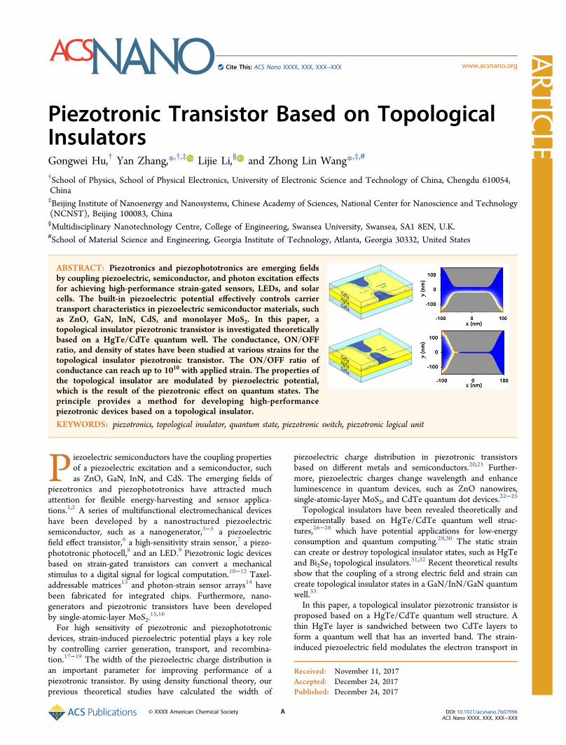
insulator, Figure 1 shows the HgTe/CdTe quantum wellstructure with a split gate on the side of HgTe. The constrictionbetween the left and right gates acts as a quantum point contact(QPC).34 The width of the quantum point contact can beturned by the piezoelectric potential. Figure 1(a) shows agapless band structure in quantum point contact without apiezoelectric potential, which is a typical topological insulatorbased on the HgTe/CdTe quantum well structure. The currentcan flow across the quantum point contact region without apiezoelectric potential. This state is the “ON” state of thisdevice. The width of the quantum point contact decreases whilethe piezoelectric potential increases. While the band gap isformed by applied strain, the conducting channel closes, asshown in Figure 1(b). Therefore, the electrons will be blockedand reflected back, resulting in an “OFF” state.A piezotronic transistor based on topological insulator is a
quantum piezotronic device, which uses a piezoelectric field tocontrol the conductance of a topological insulator. The initialstate is a topological insulator state without applied strain. Theenergy band structure of the topological insulator state changesfrom gapless to having a gap by applying strain. In the case ofthe HgTe/CdTe quantum well structure, the strain-inducedpiezoelectric field is parallel to the surface of the topologicalinsulator. The direction of the piezoelectric field also can beperpendicular to the surface of the topological insulator. Forexample, in the case of the GaN/InN/GaN quantum well
structure, the band gap becomes smaller while the strain-induced piezoelectric field increases.33 Thus, topologicalinsulator states are formed by a strain-induced piezoelectricfield.Besides the above two types of topological insulator based
piezotronic transistor, possible structures using a piezoelectricfield to control the topological insulator states are a GaAs/Ge/GaAs quantum well35 and two-dimensional transition metaldichalcogenides,36 such as MoS2, MoSe2, and WSe2.Electronic transport in the quantum well can be described by
the Schrodinger equation:
ψ ψ=H E (1)
where H is a Hamiltonian, ψ is a wave function, and E is aneigenvalue. By solving the Schrodinger equation under theboundary condition, the wave function can be obtained tocalculate the transport properties, including the density of states(DOS), the transmission, and the conductance.Taking a typical HgTe/CdTe quantum well topological
insulator as an example, the electronic properties are describedby the four-band Hamiltonian of the Bernevig−Hughes−Zhang(BHZ) model:26
ε
ε
ε
ε
=
+
−
+ −
− −
−
+
+
−
⎡
⎣
⎢⎢⎢⎢⎢⎢
⎤
⎦
⎥⎥⎥⎥⎥⎥
H k
M Ak
Ak M
M Ak
Ak M
( )
0 00 0
0 00 0
k k
k k
k k
k k (2)
where k = (kx, ky) is the in-plane momentum of electrons, εk =C + V(x) − Dk2,Mk =M − Bk2, k± = kx ± iky, k
2 = kx2 + ky
2, andV(x) is the confinement potential of the quantum well. A, B, C,D, and M are the expansion parameters describing the bandstructure of the HgTe/CdTe quantum well. The topological
Figure 1. Schematics of electronic transport and energy band controlled by the QPC in the HgTe/CdTe topological insulator. The spin-up(green line) and spin-down (purple line) electrons travel along the boundary. (a) Gapless Dirac cone for the wide QPC and (b) energy gap Egemerging for the narrow QPC.
ACS Nano Article
DOI: 10.1021/acsnano.7b07996ACS Nano XXXX, XXX, XXX−XXX
B
property of the HgTe/CdTe quantum well depends on thethickness of the HgTe layer, which has the critical value dc.
26
While the thickness is less than the critical thickness dc, thequantum well is the normal insulator state. When the thicknessis larger than dc, the band energy of the quantum well is thetopological insulator state. In this study, the thickness of HgTeis set at 7 nm (>dc = 6.3 nm), a typical value for a topologicalinsulator state of the device. The material parameters used inthis study are A = 364.5 meV nm, B = −686 meV nm2, C = 0, D= −512 meV nm2, and M = −10 meV.26
The conductance is given from Landauer−Buttiker for-mula:37,38
∑= | |G G tm n
nm0,
2
(3)
where tnm is the transmission coefficient for an electron fromthe nth input mode to the mth output mode and G0 is theconductance quantum, which is defined as e2/h.For a small uniform mechanical strain S, the polarization
vector P is given by39
=P e S( ) ( ) ( )i ijk jk (4)
where eijk the third-order tensor is the piezoelectric tensor.According to piezoelectric theory, the constituting equations
can be given by17,40
σ = −
= +
⎪
⎪
⎧⎨⎩
c S e E
D eS kE
TE
(5)
where σ and cE are the stress and elasticity tensor, E and D arethe electric field and displacement, and k is the dielectric tensor.Thus, piezoelectric potential induced by applied strain can be
obtained as
ε ε=V
PLpiezo
piezo
r 0 (6)
where Lpiezo is the length of the piezoelectric material, εr is therelative dielectric constant, and ε0 is the vacuum dielectricconstant.Considering zinc-blende structure CdTe grown along the
[111] direction41 with shear strain s23 of the y−z plane, thepiezoelectric potential is given by
ε ε=V
e s Lpiezo
14 23 CdTe
r 0 (7)
where e14 is the piezoelectric coefficient of CdTe and LCdTe isthe length of CdTe in topological insulator.For the wurtzite structure GaN42 with strain s11, s22, and s33
along the x, y, and z directions, the piezoelectric potential canbe given by
ε ε=
+ +V
e s e s e s L( )piezo
33 33 31 11 31 22 GaN
r 0 (8)
where LGaN is the length of GaN in the topological insulator.
RESULTS AND DISCUSSIONPiezotronic Transistor Based on a Topological
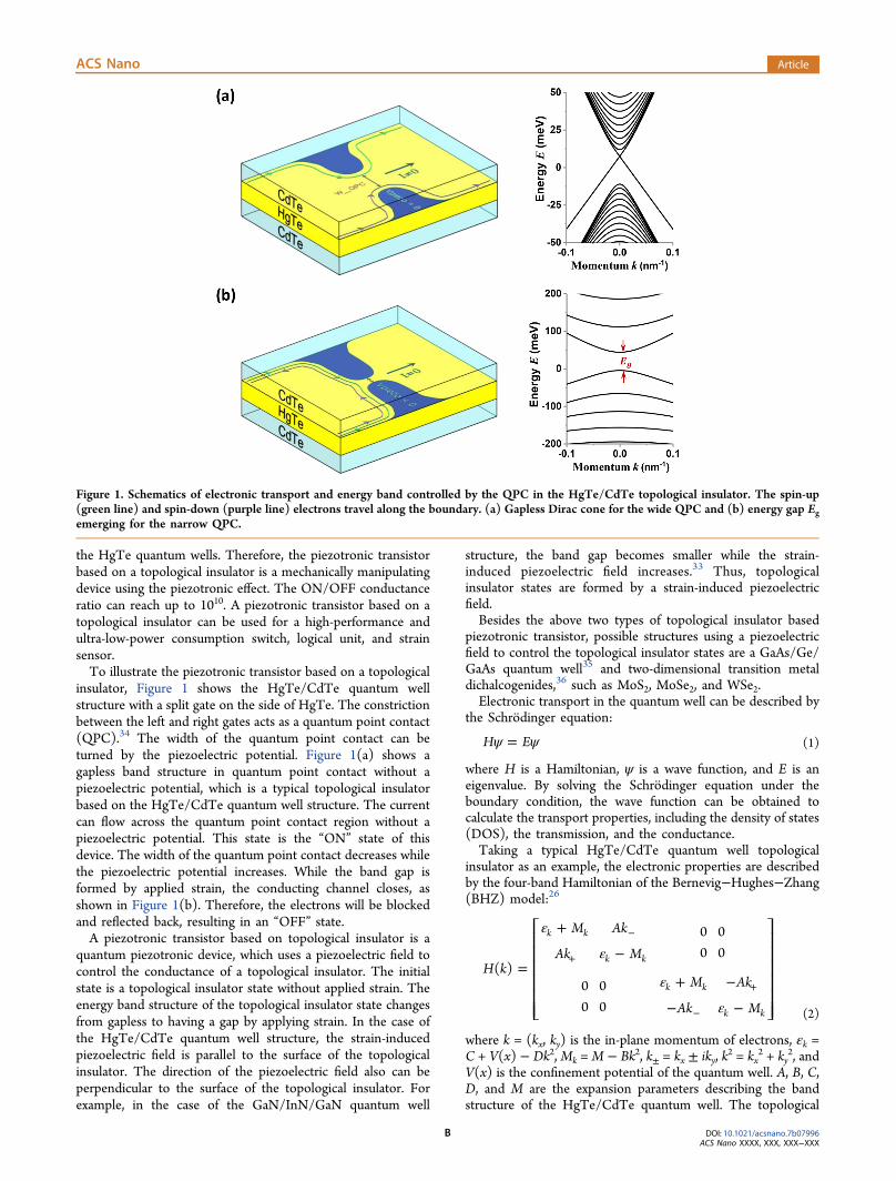
Insulator. Figure 2(a) shows a schematic of the strainmodulation of electron transport in a quantum well. Thestrain-induced piezoelectric potential is applied on the left andright gate, which is located on the top of the HgTe/CdTequantum well.43 The split gate can affect the extension of thedepletion regions of the quantum well,44 which can restrictelectrons traveling through the system. In HgTe/CdTequantum well structure topological insulator based piezotronicdevices, the split gate voltage is supplied by the piezoelectricpotential and bias voltage.
Figure 2. (a) Schematic of controlling the width of the QPC by left and right gate voltage on the top CdTe layer. (b) Piezoelectric potential asa function of strain under different piezoelectric semiconductor materials (CdTe, GaAs, GaP, InSb, and InAs). (c) Width of the QPC as afunction of strain. (d) Conductance as a function of strain at fixed Fermi energy EF = 10 meV.
ACS Nano Article
DOI: 10.1021/acsnano.7b07996ACS Nano XXXX, XXX, XXX−XXX
C
For wurtzite structure GaN/InN/GaN quantum well, tensile,and compressive strain can induce piezoelectric charges in theinterface, and a perpendicular piezoelectric field is created inthe quantum well. The piezoelectric field will change thenormal insulator state to a topological insulator state in theGaN/InN/GaN quantum well.The HgTe/CdTe quantum well is a good candidate for a
topological insulator for a quantum piezotronic device. Thesubstrate of the HgTe/CdTe quantum well can be designed byzinc-blende structure piezoelectric semiconductors, such asGaAs, GaP, InSb, and InAs. According to the piezoelectricequation, the polarization charges can be obtained from eqs 4and 5. The piezoelectric coefficient e14 and relative dielectricconstant εs are listed in Table 1.45
In the case of a piezoelectric field parallel to the surface of thetopological insulator, the width of the QPC can be effectivelycontrolled by applied strain on the piezoelectric semiconductor.Previous experiments showed that the width of the QPC(WQPC) is approximately linearly dependent on the split-gatevoltage.46 Therefore, WQPC is proportional to piezoelectricpotential in the QPC region, which is given by
α= + +W V V W( )QPC piezo 0 0 (9)
where α is the parameter depending on the topologicalinsulator material and device structure, V0 is the bias voltagebetween the left and right gate, andW0 is the width of the QPCwithout piezoelectric potential. The parameters used in thecalculation are α = 225 nm V−1, V0 = 0.87 V, and W0 = 300nm.46
The piezoelectric potential is a linear function of shear strains23 with different piezoeletric semiconductors, as shown inFigure 2(b). The piezoelectric potential increases with appliedstrain for CdTe. Due to the opposite sign of the piezoelectriccoefficient, the piezoelectric potential decreases with strain forGaAs, GaP, InSb, and InAs. Figure 2(c) shows the width of theQPC at various strain from −2.0% to 2.0%.In our simulation, the Fermi energy is EF = 10 meV. At this
condition, the system has one topological edge channel. Figure2(d) shows that the conductance G changes with external strains23. The conductance changes from “ON” to “OFF” state at astrain of −1.5% in the case of CdTe. While applied strain islarger than the switching point, the band gap Eg appears. As aresult, the electrons are blocked. In addition, the energy bandshows a gapless structure of a topological insulator, whileapplied strain is less than the switching point. For GaAs, GaP,InSb, and InAs, the strain switching point is 0.36%, 0.54%,1.21%, and 1.75%, respectively. Thus, the conductance can beeffectively controlled by strain. This is the piezotronic effect onthe topological insulator. The ON/OFF ratio of theconductance is up to1010. Therefore, the strain-gatedpiezotronic transistor offers a high-performance and low-power consumption strain-gated switch, which can act as astrain-gated logic unit.The design of a topological insulator piezotronic switch is
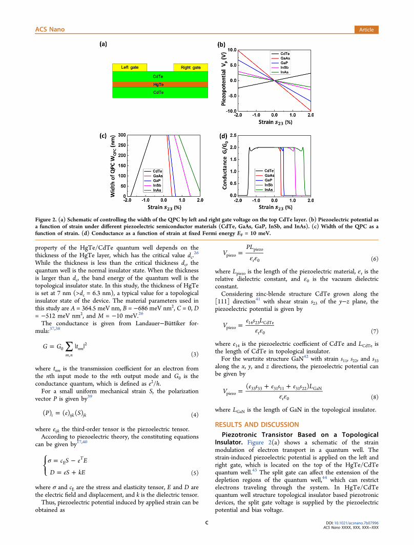
shown in Figure 3(a). The piezoelectric potential and biasvoltage are applied to the gate. The strain applied on thepiezoelectric semiconductor CdTe is plotted as a function oftime in Figure 3(b). The strain varies from −1.6% to −1.0%.
Table 1. Piezoelectric Coefficient and Relative DielectricConstant for the Crystals of Cubic Symmetry
materialpiezoelectric coefficient e14
(C/m2)relative dielectric
constant, εr ref
CdTe 0.035 9.8 41GaAs −0.16 11 45GaP −0.1 10 45InSb −0.071 16 45InAs −0.045 14.5 45
Figure 3. (a) Schematic of a piezotronic switch based on a topological insulator. The output signal 1 is the “ON” state and 0 is the “OFF”state. (b) Applied strain, conductance, and output signals change with time. (c) Maximum value of sensitivity for different piezoelectricsemiconductor materials. (d) Sensitivity versus strain.
ACS Nano Article
DOI: 10.1021/acsnano.7b07996ACS Nano XXXX, XXX, XXX−XXX
D
The conductance changes from near zero to 2G0, correspond-ing to the “OFF” and “ON” state, respectively.The sensitivity of the piezotronic strain sensor can be
calculated by
=RG G
sd( / )
d0
23 (10)
The maximum values of sensitivity and corresponding strain areshown in Figure 3(c). It clearly shows that the maximumsensitivity is larger than 103, For GaAs and GaP, the maximumvalue of sensitivity can reach over 104. Figure 3(d) shows theswitch and strain sensor region divided by the sensitivity. Theamplitude of the sensitivity sharply changes at the sensorregion.Piezotronic Effect on Surface States of a Topological
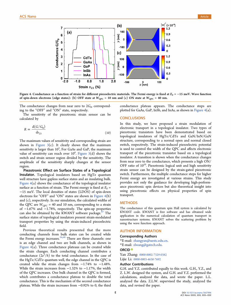
Insulator. Topological insulators based on HgTe quantumwell structure have gapless surface states and an insulating bulk.Figure 4(a) shows the conductance of the topological insulatorsurface as a function of strain. The Fermi energy is fixed at EF =−15 meV. The local densities of states (LDOS) of spin-downelectrons for “OFF” and “ON” states are shown in Figure 4(b)and (c), respectively. In our simulation, the calculated widths ofthe QPC are WQPC = 40 and 10 nm, corresponding to a strainof −1.67% and −1.78%, respectively. The spin-up propertiescan also be obtained by the KWANT software package.47 Thesurface states of topological insulators present strain-modulatedtransport properties by using the strain-induced piezoelectricfield.Previous theoretical results presented that the more
conducting channels from bulk states can be created whilethe Fermi energy increases.34,48 There are three channels: oneis an edge channel and two are bulk channels, as shown inFigure 4(a). Three conductance plateaus can be created whilethe strain changes. Each conducting channel contributes aconductance (2e2/h) to the total conductance. In the case ofthe HgTe/CdTe quantum well, the edge channel in the QPC iscreated while the strain changes from −1.74% to −1.48%.While the strain increases from −1.32% to −1.17%, the widthof the QPC increases. One bulk channel in the QPC is formed,which contributes a conductance plateau to double the totalconductance. This is the mechanism of the second conductanceplateau. While the strain increases from −0.92% to 0, the third
conductance plateau appears. The conductance steps areplotted for GaAs, GaP, InSb, and InAs, as shown in Figure 4(a).
CONCLUSIONSIn this study, we have proposed a strain modulation ofelectronic transport in a topological insulator. Two types ofpiezotronic transistors have been demonstrated based ontopological insulators of HgTe/CdTe and GaN/InN/GaNstructure, corresponding to a normal open and normal closedswitch, respectively. The strain-induced piezoelectric potentialis used to control the width of the QPC and affects electronictransport of the piezotronic transistor based on a topologicalinsulator. A transition is shown when the conductance changesfrom near zero to the conductance, which presents a high ON/OFF ratio of 1010. Piezotronic logical unit and high sensitivitystrain sensor can be designed by the strain-gated piezotronicswitch. Furthermore, the multiple conductance steps for higherFermi energy are investigated at various strains. This studyprovides not only the guidance for developing high-perform-ance piezotronic spin devices but also theoretical insight intousing piezotronic effects on physical properties of spintransport.
METHODSThe conductance of this quantum spin Hall system is calculated byKWANT code. KWANT is free software and has obtained wideapplication in the numerical calculation of quantum transport innanostructure systems. KWANT solves the scattering problem byusing the wave function approach.
AUTHOR INFORMATIONCorresponding Authors*E-mail: [email protected].*E-mail: [email protected] Zhang: 0000-0002-7329-0382Lijie Li: 0000-0003-4630-7692Author ContributionsG.H. and Y.Z. contributed equally to this work. G.H., Y.Z., andZ. L.W. designed the system, and G.H. and Y.Z. performed thecalculations, analyzed the data, and wrote the paper. L.L.analyzed the data. Z.L.W. supervised the study, analyzed thedata, and revised the paper.
Figure 4. Conductance as a function of strain for different piezoelectric materials. The Fermi energy is fixed at EF = −15 meV. Wave functionof spin-down electrons (edge states): (b) OFF state at WQPC = 10 nm and (c) ON state at WQPC = 40 nm.
ACS Nano Article
DOI: 10.1021/acsnano.7b07996ACS Nano XXXX, XXX, XXX−XXX
E
NotesThe authors declare no competing financial interest.
ACKNOWLEDGMENTS
The authors are thankful for the support from University ofElectronic Science and Technology of China (ZYGX2015-KYQD063), Swansea University, the SPARC II project, theAgorIP project, the Innovate UK, and Thousand TalentsProgram for a Pioneer Researcher and His Innovation Team,China.
REFERENCES(1) Wang, Z. L. Progress in Piezotronics and Piezo-phototronics.Adv. Mater. 2012, 24, 4632−4646.(2) Wu, W.; Wang, Z. L. Piezotronics and Piezo-phototronics forAdaptive Electronics and Optoelectronics. Nat. Rev. Mater. 2016, 1,16031.(3) Wang, Z. L.; Song, J. Piezoelectric Nanogenerators Based on ZincOxide Nanowire Arrays. Science 2006, 312, 242−246.(4) Qin, Y.; Wang, X.; Wang, Z. L. Microfibre−nanowire HybridStructure for Energy Scavenging. Nature 2008, 451, 809−813.(5) Wang, X.; Song, J.; Liu, J.; Wang, Z. L. Direct-currentNanogenerator Driven by Ultrasonic Waves. Science 2007, 316,102−105.(6) Wang, X.; Zhou, J.; Song, J.; Liu, J.; Xu, N.; Wang, Z. L.Piezoelectric Field Effect Transistor and Nanoforce Sensor Based on aSingle ZnO Nanowire. Nano Lett. 2006, 6, 2768−2772.(7) Zhou, J.; Gu, Y.; Fei, P.; Mai, W.; Gao, Y.; Yang, R.; Bao, G.;Wang, Z. L. Flexible Piezotronic Strain Sensor. Nano Lett. 2008, 8,3035−3040.(8) Hu, Y.; Zhang, Y.; Chang, Y.; Snyder, R. L.; Wang, Z. L.Optimizing the Power Output of a ZnO Photocell by Piezopotential.ACS Nano 2010, 4, 4220−4224.(9) Yang, Q.; Wang, W.; Xu, S.; Wang, Z. L. Enhancing LightEmission of ZnO Microwire-based Diodes by Piezo-phototronicEffect. Nano Lett. 2011, 11, 4012−4017.(10) Wu, W.; Wei, Y.; Wang, Z. L. Strain-gated Piezotronic LogicNanodevices. Adv. Mater. 2010, 22, 4711−4715.(11) Yu, R.; Wu, W.; Ding, Y.; Wang, Z. L. GaN Nanobelt-basedStrain-gated Piezotronic Logic Devices and Computation. ACS Nano2013, 7, 6403−6409.(12) Yu, R. M.; Wu, W. Z.; Pan, C. F.; Wang, Z. N.; Ding, Y.; Wang,Z. L. Piezo-phototronic Boolean Logic and Computation UsingPhoton and Strain Dual-gated Nanowire Transistors. Adv. Mater.2015, 27, 940−947.(13) Wu, W.; Pan, C.; Zhang, Y.; Wen, X.; Wang, Z. L. Piezotronicsand Piezo-phototronics: From Single Nanodevices to Array of Devicesand Then to Integrated Functional System. Nano Today 2013, 8, 619−642.(14) Pan, C. F.; Dong, L.; Zhu, G.; Niu, S. M.; Yu, R. M.; Yang, Q.;Liu, Y.; Wang, Z. L. High-resolution Electroluminescent Imaging ofPressure Distribution Using a Piezoelectric Nanowire LED Array. Nat.Photonics 2013, 7, 752−758.(15) Wu, W.; Wang, L.; Li, Y.; Zhang, F.; Lin, L.; Niu, S.; Chenet, D.;Zhang, X.; Hao, Y.; Heinz, T. F.; et al. Piezoelectricity of Single-atomic-layer MoS2 for Energy Conversion and Piezotronics. Nature2014, 514, 470−474.(16) Liu, W.; Zhang, A.; Zhang, Y.; Wang, Z. L. Density FunctionalStudies on Edge-contacted Single-layer MoS2 Piezotronic Transistors.Appl. Phys. Lett. 2015, 107, 083105.(17) Zhang, Y.; Liu, Y.; Wang, Z. L. Fundamental Theory ofPiezotronics. Adv. Mater. 2011, 23, 3004−3013.(18) Zhang, Y.; Wang, Z. L. Theory of Piezo-phototronics for Light-emitting Diodes. Adv. Mater. 2012, 24, 4712−4718.(19) Zhang, Y.; Yang, Y.; Wang, Z. L. Piezo-phototronics Effect onNano/Microwire Solar Cells. Energy Environ. Sci. 2012, 5, 6850−6856.
(20) Liu, W.; Zhang, A. H.; Zhang, Y.; Wang, Z. L. First PrincipleSimulations of Piezotronic Transistors. Nano Energy 2015, 14, 355−363.(21) Liu, W.; Zhang, A.; Zhang, Y.; Wang, Z. L. Density FunctionalStudies on Wurtzite Piezotronic Transistors: Influence of DifferentSemiconductors and Metals on Piezoelectric Charge Distribution andSchottky Barrier. Nanotechnology 2016, 27, 205204.(22) Zhang, Y.; Li, L. Piezophototronic Effect EnhancedLuminescence of Zinc Oxide Nanowires. Nano Energy 2016, 22,533−538.(23) Li, L.; Zhang, Y. Simulation of Wavelength Selection Using ZnONanowires Array. J. Appl. Phys. 2017, 121, 214302.(24) Li, L.; Zhang, Y. Controlling the Luminescence of MonolayerMoS2 Based on the Piezoelectric Effect. Nano Res. 2017, 10, 2527−2534.(25) Zhang, Y.; Nie, J.; Li, L. Piezotronic Effect on the Luminescenceof Quantum Dots for Micro/Nano-newton Force Measurement. NanoRes. 2017, DOI: 10.1007/s12274-017-1814-x.(26) Bernevig, B. A.; Hughes, T. L.; Zhang, S. C. Quantum Spin HallEffect and Topological Phase Transition in HgTe Quantum Wells.Science 2006, 314, 1757−1761.(27) Konig, M.; Wiedmann, S.; Brune, C.; Roth, A.; Buhmann, H.;Molenkamp, L. W.; Qi, X. L.; Zhang, S. C. Quantum Spin HallInsulator State in HgTe Quantum Wells. Science 2007, 318, 766−770.(28) Chang, C.-Z.; Zhang, J.; Feng, X.; Shen, J.; Zhang, Z.; Guo, M.;Li, K.; Ou, Y.; Wei, P.; Wang, L.-L.; et al. Experimental Observation ofthe Quantum Anomalous Hall Effect in a Magnetic TopologicalInsulator. Science 2013, 340, 167−170.(29) Murakami, S.; Nagaosa, N.; Zhang, S. C. DissipationlessQuantum Spin Current at Room Temperature. Science 2003, 301,1348−1351.(30) Qi, X.-L.; Zhang, S.-C. Topological Insulators and Super-conductors. Rev. Mod. Phys. 2011, 83, 1057−1110.(31) Liu, Y.; Li, Y. Y.; Rajput, S.; Gilks, D.; Lari, L.; Galindo, P. L.;Weinert, M.; Lazarov, V. K.; Li, L. Tuning Dirac States by Strain in theTopological Insulator Bi2Se3. Nat. Phys. 2014, 10, 294−299.(32) Brune, C.; Liu, C. X.; Novik, E. G.; Hankiewicz, E. M.;Buhmann, H.; Chen, Y. L.; Qi, X. L.; Shen, Z. X.; Zhang, S. C.;Molenkamp, L. W. Quantum Hall Effect from the Topological SurfaceStates of Strained Bulk HgTe. Phys. Rev. Lett. 2011, 106, 126803.(33) Miao, M. S.; Yan, Q.; Van de Walle, C. G.; Lou, W. K.; Li, L. L.;Chang, K. Polarization-driven Topological Insulator Transition in aGaN/InN/GaN Quantum Well. Phys. Rev. Lett. 2012, 109, 186803.(34) Zhang, L. B.; Cheng, F.; Zhai, F.; Chang, K. Electrical Switchingof the Edge Channel Transport in HgTe Quantum Wells with anInverted Band Structure. Phys. Rev. B: Condens. Matter Mater. Phys.2011, 83, 081402.(35) Zhang, D.; Lou, W.; Miao, M.; Zhang, S. C.; Chang, K.Interface-induced Topological Insulator Transition in GaAs/Ge/GaAsQuantum Wells. Phys. Rev. Lett. 2013, 111, 156402.(36) Qian, X.; Liu, J.; Fu, L.; Li, J. Solid state theory. Quantum SpinHall Effect in Two-dimensional Transition Metal Dichalcogenides.Science 2014, 346, 1344−1347.(37) Landauer, R. Spatial Variation of Currents and Fields Due toLocalized Scatterers in Metallic Conduction. IBM J. Res. Dev. 1957, 1,223−231.(38) Landauer, R. Electrical Transport in Open and Closed Systems.Z. Phys. B: Condens. Matter 1987, 68, 217−228.(39) Maugin, G. A. Continuum Mechanics of Electromagnetic Solids;North-Holland: Amsterdam, 1998.(40) Ikeda, T. Fundamentals of Piezoelectricity; Oxford UniversityPress: UK, 1990; p 158.(41) Andre, R.; Cibert, J.; Dang, L. S.; Zeman, J.; Zigone, M.Nonlinear Piezoelectricity: The Effect of Pressure on CdTe. Phys. Rev.B: Condens. Matter Mater. Phys. 1996, 53, 6951−6954.(42) Bernardini, F.; Fiorentini, V.; Vanderbilt, D. SpontaneousPolarization and Piezoelectric Constants of III-V Nitrides. Phys. Rev. B:Condens. Matter Mater. Phys. 1997, 56, 10024−10027.
ACS Nano Article
DOI: 10.1021/acsnano.7b07996ACS Nano XXXX, XXX, XXX−XXX
F
(43) Wu, Z. H.; Lin, L. Z.; Yang, W.; Zhang, D.; Shen, C.; Lou, W.;Yin, H.; Chang, K. Spin-polarized Charge Trapping Cell Based on aTopological Insulator Quantum Dot. RSC Adv. 2017, 7, 30963−30969.(44) Bird, J. P. Electron Transport in Quantum Dots; Kluwer: Boston,2003.(45) Bright, V. M.; Hunt, W. D. Bleustein−Gulyaev Waves inGallium Arsenide and Other Piezoelectric Cubic Crystals. J. Appl. Phys.1989, 66, 1556−1564.(46) van Wees, B. J.; van Houten, H.; Beenakker, C. W.; Williamson,J. G.; Kouwenhoven, L. P.; van der Marel, D.; Foxon, C. T. QuantizedConductance of Point contacts in a Two-dimensional Electron Gas.Phys. Rev. Lett. 1988, 60, 848−850.(47) Groth, C. W.; Wimmer, M.; Akhmerov, A. R.; Waintal, X.Kwant: A Software Package for Quantum Transport. New J. Phys.2014, 16, 063065.(48) Krueckl, V.; Richter, K. Switching Spin and Charge betweenEdge States in Topological Insulator Constrictions. Phys. Rev. Lett.2011, 107, 086803.
ACS Nano Article
DOI: 10.1021/acsnano.7b07996ACS Nano XXXX, XXX, XXX−XXX
G