Embed Size (px)
Citation preview

JOURNAL OF LIGHTWAVE TECHNOLOGY, VOL. 21, NO. 12, DECEMBER 2003 3085
Photonic Time-Stretched Analog-to-DigitalConverter: Fundamental Concepts and
Practical ConsiderationsYan Han and Bahram Jalali, Fellow, IEEE
Invited Paper
Abstract—Ultra-wide-band analog-to-digital (A/D) conversionis one of the most critical problems faced in communication, instru-mentation, and radar systems. This paper presents a comprehen-sive analysis of the recently proposed time-stretched A/D converter.By reducing the signal bandwidth prior to digitization, this tech-nique offers revolutionary enhancements in the performance ofelectronic converters. The paper starts with a fundamental-physicsanalysis of the time–wavelength transformation and the implica-tion of time dilation on the signal-to-noise ratio. A detailed mathe-matical description of the time-stretch process is then constructed.It elucidates the influence of linear and nonlinear optical disper-sion on the fidelity of the electrical signal. Design issues of a single-sideband time-stretch system, as they relate to broad-band opera-tion, are examined. Problems arising from the nonuniform opticalpower spectral density are explained, and two methods for over-coming them are described. As proof of the concept, 120 GSa/sreal-time digitization of a 20-GHz signal is demonstrated. Finally,design issues and performance features of a continuous-time time-stretch system are discussed.
Index Terms—Analog-to-digital (A/D) conversion, microwavephotonics, optical signal processing, single-sideband (SSB) mod-ulation, time stretch.
I. INTRODUCTION
D IGITAL signal processing (DSP) has revolutionizedmodern communication and radar systems by offering
unprecedented performance and adaptivity. For broad-bandsystems, however, the application of DSP is hindered bydifficulty in capturing the wide-band signal [1]. A samplingoscilloscope is not an option because it requires the signal tobe repetitive in time. It only provides information about theaverage signal behavior; hence, it does not operate in real time.The real-time capture of ultrafast electrical signals is a difficultproblem that requires wide-band analog-to-digital converters(ADCs).
Manuscript received April 15, 2003; revised July 29, 2003. This work wassupported by the Defense Advanced Research Project Agency (DARPA) underthe Photonic Analog-to-Digital Converter (PACT) program.
The authors are with Optoelectronic Circuits and Systems Laboratory, De-partment of Electrical Engineering, University of California at Los Angeles,Los Angeles, CA 90095 USA (e-mail: [email protected]).
Digital Object Identifier 10.1109/JLT.2003.821731
Fig. 1. Conventional sample-interleaved ADC architecture. The signal iscaptured by a parallel array of slow digitizer, each clocked at a fraction ofthe Nyquist rate. The Nyquist criterion is only satisfied when the signal isreconstructed, sample-by-sample, in the digital domain.
A detailed discussion on the limits of electronic ADCs is be-yond the scope of this paper [2]. Simply stated, the performanceis limited by one or more of the following problems:
1) jitter in the sampling clock;2) settling time of the sample-and-hold circuit;3) speed of the comparator (comparator ambiguity);4) mismatches in the transistor thresholds and passive com-
ponent values.The limitations imposed by all these factors become more severeat higher frequencies.
The standard approach to deal with this problem is to em-ploy parallelism through the use of the time-interleaved ADCarchitecture, shown in Fig. 1 [3], [4]. Here, the signal is cap-tured by a parallel array of slow digitizers, each clocked at afraction of the Nyquist rate. The Nyquist criterion is only satis-fied when the signal is reconstructed, sample-by-sample, in thedigital domain. In this paper, we use the term “sample-inter-leaved” to refer to this architecture. It is well known that mis-matches between digitizers limit the dynamic range and, hence,the resolution of sample-interleaved ADC systems [3], [4]. Astate-of-the-art electronic ADC, embodied by real-time digi-tizing oscilloscopes (Tektronix TDS7404, or Agilent 54 854A)boasts 20 GSa/s 4-GHz analog bandwidth. Depending on the
0733-8724/03$17.00 © 2003 IEEE

3086 JOURNAL OF LIGHTWAVE TECHNOLOGY, VOL. 21, NO. 12, DECEMBER 2003
(a)
(b)
Fig. 2. Conceptual block diagram for the time-stretched ADC. (a)Single-channel system for capturing a time-limited signal. (b) Multichannelsystem for capturing a continuous-time signal. In contrast to thesample-interleaved system (Fig. 1), each channel here is sampled at orabove the Nyquist rate.
input signal amplitude, these instruments exhibit an effectivenumber-of-bits (ENOB) of approximately 4–5.5 b, measuredover the full bandwidth.
An entirely new A/D architecture is the so-calledtime-stretchedADC, shown in Fig. 2[5]–[7]. Here, the analogsignal is slowed down prior to sampling and quantization by anelectronic digitizer. For a time-limited input, a single channel,shown in Fig. 2(a), suffices. A continuous-time input can becaptured with a multichannel system, as shown in Fig. 2(b).The partitioning of the continuous signal into parallel segmentsdoes not necessarily require electronic switches. As discussedsubsequently in this paper, it can be performed passively in theoptical domain.
Slowing down the signal prior to digitization has several ad-vantages. For a stretch factor of, the effective sampling rateof the electronic digitizer is increased to . The effectiveinput bandwidth of the electronic digitizer is also increased by
. The error associated with the jitter in the sampling clock ofthe digitizer is reduced due to a reduction in the signal slew rate,a key feature not shared by the conventional sample-interleavedarchitecture. For a time-limited input, only a single digitizeris needed [Fig. 2(a)]. Hence, interchannel mismatch problemsare avoided as there is no need to use multiple digitizers. Forthe continuous-time system [Fig. 2(b)], one would expect thesimilar interchannel mismatches; however, it has recently beenshown that mismatch errors can be corrected using the infor-mation available in the signal [8]. This is another advantage ofthetime-stretchedADC (TS-ADC) over thesample-interleavedADC. It exploits a fundamental difference between the two sys-tems: in the former, the signal at each channel is sampled at orabove the Nyquist rate, whereas in the latter, it is sampled at afraction of the Nyquist rate.
A practical method for implementing the time-stretch func-tion is to use the photonic technique shown in Fig. 3 [7], [9].
A linearly chirped optical pulse is generated by propagatingthe broad-band (nearly transform-limited) pulses generated bya SC source [10] in a chromatic dispersive medium, such asthe single-mode fiber (SMF). The electrical input signal modu-lates the intensity of the chirped optical pulses in an electroopticmodulator (EOM). The envelope is subsequently stretched in asecond spool of fiber before photodetection and digitization bya moderate-speed electronic ADC.
This paper discusses fundamental and practical considera-tions of time-stretched ADC. Section II explains the validityof the linear time–wavelength mapping, a central assumptionin the time-stretch technique. The influence of time stretchingon an electrical signal-to-noise ratio (SNR) is discussed in thenext section. Section IV describes a detailed analytical modelfor the time-stretch process that reveals the effects of linear andnonlinear fiber dispersion on the fidelity of the time-stretchedsignal. Section V provides an explanation of the time–band-width product (TBP), and its dependence on physical system pa-rameters. It identifies the limit on the TBP set by dispersion andidentifies single-sideband (SSB) modulation as a means to mit-igate it. In Section VI, practical limitation of SSB modulationis discussed, and it is shown that an ultra-wide-band system canbe constructed using commercially available components. Sec-tion VII describes the differential time-stretch technique and itsability to remove distortion caused by spectral nonuniformityand pulse-to-pulse variations of the optical source. Finally, Sec-tion VIII discusses the fundamental and practical considerationsfor continuous-time operation of the time-stretch ADC.
II. TIME–WAVELENGTH MAPPING
An intuitive approach to understanding the time-stretchprocess is through the time–wavelength mapping represen-tation. The stretch process consists of two steps. Step 1 isthe time-to-wavelength (-to- ) mapping performed by thecombination of the chirped optical pulse and the EOM. Asshown in the subset of Fig. 3, 1-ps pulses generated by apassively mode-locked fiber laser at 1560 nm are used togenerate broad-band supercontinuum (SC) in three stages offibers after the amplification [10]. An optical bandpass filteris placed after SC generation to slice a suitable portion fortime stretching. The so-obtained nearly transform-limitedoptical pulse is chirped after propagating through a dispersivemedium. When this chirped pulse is modulated by an intensitymodulator, the time-domain signal is mapped into wavelengthdomain. Step 2 is the wavelength-to-time (-to- ) mappingperformed by the second fiber. The modulated chirped pulsepropagates through a second dispersive medium. As a result,the signal modulated onto the chirp pulse is stretched in thetime as the pulse is further chirped.
The validity of time–wavelength representation can be under-stood through the following argument. Suppose that the chirpedpulse is obtained by linearly dispersing a transform-limitedpulse of the width . This represents the system’s timeresolution; in other words, time cannot be localized beyond
. Hence, the wavelength-to-time mapping picture is onlyvalid when the time scale of interest is sufficiently larger thanthis time ambiguity. The time scale of interest depends on

HAN AND JALALI: PHOTONIC TIME-STRETCHED A/D CONVERTER: FUNDAMENTAL CONCEPTS AND PRACTICAL CONSIDERATIONS 3087
Fig. 3. Functional block diagram for the photonic time-stretch preprocessor. A linearly chirped optical pulse is obtained by dispersing an ultra-shortultra-wide-band pulse (the SC). Time-to-wavelength mapping is achieved when this pulse is intensity-modulated by the electrical signal. The insetis the diagramof a three-stage SC generation. SC: Supercontinuum. PD: Photodetector.
the speed of the electrical signal. The well-known Nyquistsampling theorem states that it is enough to sample a band-lim-ited signal with the maximum frequency at the sampleinterval of , without the loss of information.To map the time scale of an electrical signal with frequency
to optical wavelength, it is required that .Fundamentally, is related to the optical bandwidthby the uncertainty principle . Relating opticaland electrical bandwidths, the combination of uncertainty andNyquist principles imply that the time–wavelength mappingrepresentation is valid as long as . Typically,
is in the terahertz range, whereas is in the gigahertzrange. Therefore, the assumption is readily justified.
The time-stretch system, as described previously, relies onthe linear group-velocity dispersion (GVD) characterized by theGVD parameter to linearly stretch the radio-frequency (RF)waveform in time. However, it is well known that the opticalfiber possesses nonlinear GVD, i.e., GVD is a function of wave-length. The wavelength dependence of GVD is characterizedby the higher order terms in the expansion ofas a functionof frequency, namely, , , etc. Wavelength-dependent GVDmay distort the RF signal since different time segments may bestretched by different amounts. In other words, the stretch factorcan be time dependent. In this section, we analyze this phenom-enon and demonstrate that the nonlinear dispersion has no effecton the stretch factor in the time-stretch system. This fortuitouseffect occurs because the effect in the two fibers counteract.
The GVD in optical fibers is conveniently described interms of the dispersion parameter . As an example,we consider for the SMF-28 fiber, which in units ofpicoseconds/kilometers/nanometers is given by (according tothe Corning SMF-28 product information sheet)
(1)
where is the zero-dispersion wavelength andis dispersionslope at . After traveling through a unit length of fiber, thetime–wavelength transformation is governed by the GVD. Thegroup delay per unit length is described by
where represents the reference wavelength. Then, at theinput to the modulator, the input time scale is related to thewavelength as
(2)
where is the length of the first fiber and is the forthe fiber 1. At the output of fiber 2, the output time scale andwavelength are related by
(3)
where is the second fiber length and is the for thefiber 2. It can be clearly seen that as long as the two fibers haveidentical dispersion characteristics ( ), the time trans-formation from the input to output is linear and can be simplydescribed by
(4)
where we define the magnification factor (or the stretch factor). The wavelength dependence of GVD (de-
scribed by and higher order terms) are cancelled and, hence,do not cause a nonuniform stretch.

3088 JOURNAL OF LIGHTWAVE TECHNOLOGY, VOL. 21, NO. 12, DECEMBER 2003
Fig. 4. Graphical description of the time–wavelength transformation. (a) Input signal. (b) Time–wavelength transfer function associated with nonlinear dispersionin fiber 1. (c) Input signal after time-to-wavelength mapping. (d) Wavelength–time transfer function after fiber 2. (e) Output time-stretched signal. The stretchprocess is linear (uniform) despite the nonlinear fiber dispersion.
A physical understanding can be obtained from Fig. 4, whichshows the evolution of the signal through the system. To high-light the effect of wavelength-dependent GVD, we use a value
1 ps km which is an order of magnitude higher than thatin the SMF (SMF 28). For simplicity, we consider a linear rampfor the input signal, shown in Fig. 4(a). It corresponds to the RFsignal at the modulator input in Fig. 3. Assuming operation inthe anomalous dispersion regime of the fiber, the-to- map-ping is not linear and, in particular, has positive concavity, asshown in Fig. 4(b). This results in an apparent distortion of thesignal when the time-domain signal is mapped into the wave-length domain by modulating the ramp signal on the chirpedpulse, as shown in Fig. 4(c). However, the-to- mapping in thesecond fiber has the opposite curvature, as shown in Fig. 4(d),resulting in a linear (and stretched) output after the photodetec-tion, shown in Fig. 4(e). As shown previously, this property is in-dependent of length of fibers (hence, independent of the stretchfactor) as long as the two fibers have identical dispersion behav-iors. As will be shown by a more detailed model in Section IV,
does cause another form of distortion through its interactionwith the optical modulator. In addition, small differences in thedispersion property (GVD per unit length) of the two fibers willresult in a finite amount of wavelength-dependent (and, hence,time-dependent) stretch factor.
We now summarize the key parameters of the TS-ADC: thestretch factor, time aperture, and electrical bandwidth. Through(1)–(4), it was shown that the stretch factor is given by
, or more generally, , whereand represent the total dispersion in each dispersive
element. The time aperture in a single-channel system, or thesegment length in the case of continuous-time operation (seeFig. 2), is equal to the chirped pulse duration at the modulatorinput. This is given by , where is the dis-persion parameter of fiber 1, and is the optical bandwidth.Here, it is assumed that the chirped pulsewidth is much larger
Fig. 5. Conceptual diagram of time-lens system exploiting the analogybetween paraxial diffraction and temporal dispersion. In contrast, in thetime-stretch system, the input signal is not dispersed prior to receiving thelinear chirp (or quadratic phase) due to the lack of low-loss wide-band electricaldispersive devices. The time-stretch system with the application of magnifyingan electrical signal is different than the time lens with the application ofmagnifying an optical signal.
than initial nearly transform-limited pulsewidth. As an example,assuming 20-nm optical bandwidth and 500-ps/nm dispersion(roughly equivalent to a spool of dispersion-compensating fiber(DCF) with a 3-dB total loss), the time aperture is 10 ns. An-other important system parameter is the 3-dB electrical band-width. As will be shown in Section IV, in the case of double-sideband intensity modulation, dispersion limits the 3-dB band-width to .
Finally, we point out the difference between the time-stretchsystem described here and the time-lens concept [5], [11].Shown in Fig. 5, the latter exploits the analogy betweenparaxial diffraction and temporal dispersion to magnify anoptical waveform. The input signal is first dispersed, thenlinearly chirped (quadratic phase shifted) and finally dispersedagain. For applications to A/D conversion, the input signal iselectrical. The lack of low-loss wide-band electrical dispersivedevices renders the time lens inapplicable to A/D conversion.In the time-stretch system, a linear chirp is imposed onto thesignal by the combination of the chirped optical pulse and theEOM. The input signal is not dispersed prior to receiving thelinear chirp. Hence, the system is not a time lens. The mainconsequence of this deviation from an ideal time lens is thelimitation on bandwidth of signal that can be stretched. Thistopic is discussed in Section IV.
HAN AND JALALI: PHOTONIC TIME-STRETCHED A/D CONVERTER: FUNDAMENTAL CONCEPTS AND PRACTICAL CONSIDERATIONS 3089
III. I MPACT OF TIME-STRETCH ONSNR
Intuitively, one would expect a reduction in the signal powerupon time stretching. This would be rather undesirable if it im-pacts the SNR. In this section, we analyze this phenomenonand show that, serendipitously, there is no impact on the shot-and thermal-noise-limited SNR. In addition, we show that timestretching alleviates the SNR reduction due to the jitter in thesampling clock. We also explain the impact of optical ampli-fiers when used to mitigate losses in the time-stretch system.
The shot-noise-limited SNR in a given electrical bandwidthcan be written as
(5)
where is the average photocurrent, andis the electroncharge. For a lossless system, when the signal is stretched bythe factor of , the average signal power and, hence,arereduced by in order to preserve the total energy. At the sametime, since the signal is slowed down, the required receiverbandwidth is reduced by . In other words, both the numer-ator and the denominator in (5) are reduced by the same amountfactor, rendering the unchanged.
With respect to thermal noise, the corresponding SNR isgiven by
(6)
where is the Boltzman constant, is the temperature,and are the equivalent input resistance and the total inputcapacitance of the optical-to-electrical (O/E) receiver. Aftertime stretching, both and are reduced by ; hence, thethermal-noise-limited SNR also remains unchanged.
When the analog signal is sampled prior to quantization, anadditional noise is produced by the jitter in the sampling clock.This so-called aperture uncertainty error is the main obstacle toachieving a high resolution in a high-speed A/D converter [2].The resulting SNR is related to the root-mean-square (rms) jitter
as
(7)
where is the maximum input RF signal frequency [2]. Sincetime stretch reduces into . it renders the ADC lesssensitive to jitter-induced noise in the digitizer. Quantitatively,the jitter-limited SNR improves by 6 dB per octave of timestretch. This is an important distinguishing property of the timestretch compared with time-interleaved architectures (Fig. 1).
It should be noted that in the time-stretch system, there existtwo potential types of timing jitters: optical jitter from pulsedlaser and electronic jitter from digitizer’s sampling clock. In thetime-limited application where a single digitizer is sufficient,optical jitter does not influence the system in that only a singleoptical pulse is used; therefore, the RF signal is not influencedby the jitter between optical pulses. Optical jitter does changethe absolute-time instant of samples. In a parallel time-stretchsystem where multiple segments are concatenated, optical pulse
jitter is important. The influences of interpulse timing errors onthe RF signal fidelity are discussed in detail in [8] and [12].
Since the shot- and thermal-noise-limited SNR is unaffectedby the time-stretch process, the system, from the SNR point ofview, can be treated as an RF fiber-optic link [13]. The lossesin a link generally consist of electrical-to-optical (E/O) and O/Econversion losses and insertion loss of optical components. Apractical time-stretch system uses optical amplifiers to compen-sate for the optical losses. Similar to an amplified optical link,the amplified spontaneous emission (ASE) noise is a concern.
The signal-ASE beat-noise-limited SNR can be expressed as
(8)
where is the optical signal power, is the ASE powerspectral density, and is responsivity of the PD. In addition,
is the modulation index defined as , andand are the RF voltage amplitude and the half-wave voltage,respectively. After time stretching, both and are reducedby the same factor ; hence, the signal-ASE beat-noise-limitedSNR remains unchanged.
Assuming a single optical amplifier is used, (8) can berewritten in terms of the input power of optical amplifier
(9)
where is Planck’s constant, is the optical frequency, isthe gain of the optical amplifier, and is the population in-version parameter with a value close to 2 for a typical amplifier.Compared with the thermal noise in (6), plays a sim-ilar role of . In a typical situation, 300 K, ,
1.55 m, 150 dBm Hz. This is much largerthan 168 dBm Hz and, hence, the signal-ASE beatnoise will limit the SNR of the time-stretch preprocessor. Asan example, in our current setup, the power spectral density ofSC source at the input of the first erbium-doped fiber ampli-fier (EDFA) is around 18 dBm nm with the repetition rateof 20 MHz. Assuming an optical bandwidth of 15 nm, the av-erage input power is 0.24 mW. With 40 , ,
1.58 m, 2 GHz (after stretching), the calculatedsignal-ASE beat-noise-limited SNR is 39.7, or 6.3 SNR-bits.Here, the stretched signal is assumed to occupy the pulse repeti-tion period and, hence, the signal power is equal to the averagepower. The effective bandwidth of TS-ADC will be 2 GHz timesthe stretch factor. Clearly, a SC source with a higher power spec-tral density is important to achieve a higher resolution. Every 12dB increase in power spectral density will increase the ASE-lim-ited resolution by 2 b.
The SNR analysis can be extended to the case where mul-tiple optical amplifiers are present. The treatment and conclu-sions will be similar to those in long-haul optical links with cas-caded optical amplifiers [14]. Since accumulates after cas-cading, this suggests that proper location and gain of amplifiersis critical in maximizing the SNR. This noise should become thelimiting factor if a large fiber propagating loss needs to be com-pensated. One can conclude that future development of low-loss
3090 JOURNAL OF LIGHTWAVE TECHNOLOGY, VOL. 21, NO. 12, DECEMBER 2003
highly dispersive devices will be highly valuable to the TS-ADCsystem.
IV. EFFECT OFOPTICAL DISPERSION ONFIDELITY OF THE
TIME-STRETCHEDELECTRICAL SIGNAL
While dispersion performs the desired function of timestretch, it has other influences on the electrical signals; ithas other, potentially adverse, effects as well. It is thereforeimperative to fully understand and be able to quantify theinfluence of dispersion on electrical signal fidelity. In Sec-tion IV-A below, we present the mathematical framework forthis purpose. Section IV-B investigates dispersion penalty andharmonic distortion caused by dispersion. Section IV-C revealsthe higher order effects, which we term “residual phase errors.”Finally, time stretching using SSB modulation is discussed andcompared with the DSB-modulated case.
A. Mathematical Framework
In this subsection, we develop a comprehensive mathematicalmodel for the time-stretch systems. The model is capable of pre-dicting fundamental and higher order phenomena that modifythe electrical signal during the time-stretch process.
We assume the optical SC pulse is transform-limited and hasa Gaussian envelope. In frequency domain, its electric field canbe represented as
(10)
where is the pulse half-width and is the pulse amplitude.indicates the electrical field at the output of the SC source
in Fig. 3. After propagating through the first spool of fiber, thefield becomes [15]
(11)
where and are the second-order and third-order GVD,respectively. indicates the electrical field before the modu-lator in Fig. 3. Assuming a push–pull Mach–Zehnder modulator(MZM) biased at the quadrature point, after modulation by thesinusoid RF signal of angular frequency , the field can berepresented (in time domain) as
(12)
is the electrical field at the output of modulator in Fig. 3.After propagation through the second fiber, the field becomes
(13)
is the electrical field in the PD in Fig. 3. Finally, the pho-tocurrent is given by
(14)
where , is the detector respon-sivity, is the refractive index, is the speed of light, is thevacuum permittivity, and is the fiber-effective-mode area.
Next, we analyze the signal in the electrical domain usinganalytical approximations to the previously described modeland verify their accuracy by comparison with numerical simu-lations. In Section IV-B, we consider the influence of the lineardispersion on spectrum of the electrical system. We show thatlinear dispersion will result in a frequency-dependent attenua-tion as well as frequency-dependent harmonic distortion in thetime-stretched electrical signal. In Section IV-C, we considerthe influence of nonlinear dispersion and describe the resultingresidual phase error.
B. Dispersion Penalty and Harmonic Distortion
In this subsection, we describe and quantify dispersion-in-duced power penalty and harmonic distortion in the time-stretchsystem. Since this effect originates from the linear dispersion
, we temporarily neglect the nonlinear dispersion term.Using Bessel functions, (12) can be expanded as
(15)
where evenodd .
Combining (15) with (10), (11), and (13), the electricalfield entering the PD can be written as (16), shown at thebottom of the page, where the envelope functioncorresponds to the electrical field when , and
is the dispersion-induced phase(DIP). As will be shown in this paper, DIP plays a central roleon the distortion in the stretched signal, whether in the DSB or
(16)

HAN AND JALALI: PHOTONIC TIME-STRETCHED A/D CONVERTER: FUNDAMENTAL CONCEPTS AND PRACTICAL CONSIDERATIONS 3091
SSB modulation. In obtaining (16), the following relation wasused:
In the expression for , terms related to are neglected.This is equivalent to assuming an infinite optical bandwidth or,more precisely, . This approximation is removedin the next section, and it is shown that having a finite opticalbandwidth results in a subtle phenomenon, which we term the“aperture effect.”
We now invoke the following property of Bessel func-tions: . Hence,
. We substitute (16) into (14) and for eachharmonic, we keep terms with the lowest ( ). For example,for the dc term, this requires .The photocurrent, so obtained, can be expressed as
(17)
where
is the static ( ) photocurrent, and is thedispersion length. In the case when the modulation indexissmall, (17) can be simplified into
(18)
The second term in (18) is the desired time-stretched signal,and the following terms describe undesired harmonics of it. Thedesired signal contains a frequency-dependent attenuation de-scribed by the term. For baseband signals, the systemhas a low-pass transfer function where high RF frequencies areattenuated. This is caused by interference between the beating
of carrier with the upper and the lower sidebands [7]. Qualita-tively, this penalty is similar to that observed in a conventionalRF fiber-optic link [16]. However, its magnitude is reduced bythe stretch factor appearing in [7]. The reduction in thedispersion penalty occurs because as the signal travels along thelength of the fiber, its modulation frequency is reduced, hence,a reduction in dispersion penalty. Based on the similarity of thiseffect to that in an analog optical link, SSB modulation has beenproposed as a means to mitigate this effect [17].
These results were obtained for a zero-chirp modulationachievable with a push–pull MZM, as described in (12). TheRF bandwidth will be higher when chirped modulation is em-ployed. When the chirp introduced by the modulator is oppositeto that introduced by fiber dispersion, the dispersion penaltycan be mitigated. Chirped modulation can be achieved using asingle-arm MZM biased at the quadrature point. In this case,the in (18) should be replaced by ,where the sign depends on the polarity of the bias. Whenthe sign of the first term is opposite to the second term, the3-dB RF bandwidth of the time-stretch system is equal to
, which is 41.4% larger thanthe zero-chirp case [18].
The third and forth terms in (18) are responsible for second-and third-order harmonic distortion, respectively. The ampli-tudes are for the second harmonicand for the third harmonic.Fig. 6(a) shows the fundamental and second harmonic powerin the time-stretch system with a stretch factor (dashedline) as well as the same for a conventional fiber-optic link (solidline). The latter describes a case where the RF signal is modu-lated onto a single-wavelength carrier and travels through a fiberof length . For an MZM biased at the quadrature bias point,the second harmonic is suppressed. This occurs because thesecond harmonics in the optical field spectrum are cancelled inthe PD by those arising from the beating of the upper and lowerfundamental sidebands. As the RF frequency is increased, thephase shift induced by dispersion renders this cancellation in-complete, resulting in residual second harmonic tones in the RFspectrum. The frequency dependence is periodic, as suggestedby (18). Second-order distortion is not a concern in systems op-erating in the sub-octave bandwidth regime. In addition, whilethe dispersion-induced phase shift results in second-order dis-tortion in the time-stretch system, its magnitude is far less thanthat in a conventional RF fiber-optic link.
Fig. 6(b) shows the same for the third harmonic distortion. Atvery low frequency, the third harmonic is due to the nonlineartransfer function of the modulator (biased at quadrature). Dis-persion-induced phase shift results in a periodic behavior for thethird-order distortion, as predicted by (18).
We note that in the limit of approaching infinity, the time-stretch system reduces to a conventional RF fiber-optic link,consisting of an externally modulated narrow-band source (e.g.,distributed feedback laser) that propagates over a fiber of length
. In this situation, over the limited system time aperture, thesource in the time-stretch system appears to be narrow band as inthe conventional RF fiber-optic link. Mathematically, the stretchfactor approaches unity with . Equa-tion (18) then becomes the same as the results obtained for the

3092 JOURNAL OF LIGHTWAVE TECHNOLOGY, VOL. 21, NO. 12, DECEMBER 2003
(a)
(b)
Fig. 6. (a) Electrical power transfer function for the fundamental frequencyand second harmonic distortion. (b) Same for fundamental frequency and thirdharmonic distortion. The dashed line is for the time-stretched system, andthe solid-line is for a conventional RF fiber-optic link. Calculations are forzero-chirp modulation.L = 5 km,M = 5,m = 5%.
dispersion penalty in a conventional RF fiber-optic link [16],[19].
C. Residual Phase Errors
In this subsection, we remove two assumptions made in thederivation of (18), i.e., ignoring third-order dispersion andalso terms related to in the expression for . At the sametime, the modulation is assumed linear to simplify the mathe-matical analysis.
Under the assumption of linear modulation, (12) can be sim-plified into
(19)
where is given by (11). Combining (19) with (10), (11),and (13), the signal entering the PD can be written as
(20)
where the envelope function is
Compared with the same name function in (16),terms areincluded here. As shown in (20), the optical field spectrum con-sists of DSBs at the stretched RF frequency. This is the desiredtime-stretch signal. The nonideal effects, caused by dispersion,are contained in the phase of the upper and lower stretched side-bands. For the lower ( ) and upper ( ) sidebands
(21)
where is optical bandwidth (half-width atintensity point).
The phase in (21) is composed of three terms. Thefirst term is the phase distortion due to linear dispersion,which causes attenuation at high frequencies, discussed in theprevious section. The second term is the phase distortion causedby , which combined with the first term, creates a wavelength-dependent (and, hence, time-dependent) attenuation for a givenfrequency. The third term is error caused by the finite opticalbandwidth.
The photocurrent in time domain can be expressed as (seeAppendix)
(22)
(23)
(24)
Equations (23) and (24) are the errors due toand finiteoptical bandwidth, respectively.
We now show the individual effects of these sourcesof error on a single-tone RF signal. Fig. 7(a) is a plot of
and shows the influenceof on the stretched signal, in time domain. To highlightthe impact, we use a value 10 ps km that is twoorders of magnitude higher than that in the SMF (SMF-28).As suggested by (23), this introduces a deleterious linearamplitude modulation. In the previous section, it is shownthat introduces attenuation at high RF frequencies. The

HAN AND JALALI: PHOTONIC TIME-STRETCHED A/D CONVERTER: FUNDAMENTAL CONCEPTS AND PRACTICAL CONSIDERATIONS 3093
(a)
(b)
Fig. 7. (a) Influence of nonlinear GVD, characterized by� , on thetime-stretched signal. A 100� larger� than SMF-28 is used. The behaviorcan be understood in terms of a wavelength-dependent dispersion penalty,causing higher attenuation at longer wavelengths. (b) Time-stretched outputsignal when the effect of finite optical bandwidth is included.! = 10 GHz,M = 10, � = �20 ps =km,� = 10 ps = km,L = 50 km,�� = 0.5 nm.
influence of is to make wavelength sensitive and, hence,via wavelength-to-time mapping, cause a time-dependentattenuation. To verify the validity of approximations made andconclusion of the analytical model, numerical simulations wereperformed. Fig. 8 shows the error introduced by includinginthe simulations. The functional dependence is in full agreementwith (23), verifying the validity of the approximations made inthe derivation.
Fig. 7(b) is a plot ofand shows the effect of the error introduced by the finite opticalbandwidth. For the purpose of illustration, an unusually smalloptical bandwidth of 0.5 nm is used to accentuate this effect.The envelope of this function behaves as . In an idealsituation where the optical bandwidth is much larger than theRF bandwidth ( ), this error will diminish, assuggested by (24). Typically, these errors are relatively smallto be observed in experiments as they are masked by othersources of noise and distortion, such as the quantization noiseof a wide-band electronic digitizer, the ASE noise of opticalamplifiers, and spectral nonuniformity and pulse-to-pulsevariations of the SC source.
Fig. 8. Numerical simulation result showing the error caused by nonlinearGVD. The functional dependence is in full agreement with (23), verifying thevalidity of the approximations made in the analytical model.
Fig. 9. Block diagram of the SSB-modulated photonic time-stretched A/Dconverter. The hybrid coupler provides 90RF phase shift between its twooutput ports. MZM: Mach–Zehnder modulator. SC: Supercontinuum.
D. SSB Modulation
In this subsection, we provide a complete analysis of the dis-persion-induced impairments in the case of SSB modulation.It extends the analysis reported in [17] by including the har-monic distortion (as in Section IV-B), the residual phase errors,including third-order dispersion and finite optical bandwidth (asin Section IV-C). SSB modulation can be achieved by usinga dual-arm modulator biased at the quadrature point with the
phase-shifted RF signals applied to the two arms [20]. AnSSB-modulated time-stretch system is shown in Fig. 9. Underthis modulation scheme, (12) is replaced by
(25)
Harmonic distortions in the SSB system can be obtainedthrough the same procedure as in Section IV-B by replacing(15) with
(26)

3094 JOURNAL OF LIGHTWAVE TECHNOLOGY, VOL. 21, NO. 12, DECEMBER 2003
If is small, the photocurrent can be expressed as
(27)
The first two terms describe the results reported in [17].The remaining terms are the harmonic distortion in the SSBmodulation, reported here for the first time. Clearly, thereis no -induced attenuation in the SSB system. However,a nonlinear phase distortion is introduced through the term
. In the context of TS-ADC, the phase distortion couldbe removed in the digital domain using the known dispersionbehavior of the fiber. This process is facilitated by the fact that,because interference of the sidebands is avoided, signal powerat the ADC input is preserved and, hence, this side effect istolerable. Therefore, the usefulness of the SSB technique willlargely depend on the effectiveness of digital correction of thephase distortion. In addition, harmonics distortion observed inthe DSB modulation also appears in SSB modulation.
Similarly, the residual phase distortions in the SSB systemcan be obtained through the same procedure as in Section IV-Cby replacing (19) with
(28)The photocurrent is then given by
(29)
(30)
(31)
Although the attenuation of the fundamental frequency dueto is eliminated, the errors due to and due to the finiteoptical bandwidth remain. In fact, the amplitude of these er-rors are larger in SSB modulation, by the factor com-pared with DSB modulation. This is because, in the DSB mod-ulation, the interference between two carrier-sideband beatingterms partially cancels such a distortion. In the SSB modulation,the error could also be visualized as a weak dependence of thestretch factor on the electrical signal frequency. From a disper-sion-penalty point of view, the SSB may be the preferred modu-lation method. However, the merits of DSB and SSB should becarefully examined in a particular system and for specific appli-cations.
Fig. 10. Maximum achievable TBP for a given 3-dB bandwidth, in aDSB-modulated time-stretched system. Zero-chirp modulation, achieved witha push–pull MZM, is assumed.
V. TIME–BANDWIDTH PRODUCT
A photonic time-stretch system could be describedby the following three parameters: the stretch factor,time aperture, and RF bandwidth. The stretch factoris given by . The time aperture isgiven by , where
is the optical bandwidth. The 3-dBRF bandwidth in the case of DSB modulation is equal to
for . Naturally, it is highlydesirable to maximize the time aperture. For a fixed opticalbandwidth, it is possible to do so and maintain a constantstretch factor by increasing while keeping the ratioconstant. However, a larger increases the dispersion penaltyand reduces the RF bandwidth. This tradeoff renders neitherthe time aperture nor the bandwidth capable of assessing theperformance alone. In this section, the product of time apertureand RF bandwidth is identified as an optimum metric toevaluate the overall performance and is analyzed for both DSB-and SSB-modulated time-stretch systems. This product alsohas profound significance as it reflects amounts of informationcontained in a segment. In addition, the limiting factor on thestretch factor is also discussed.
A. TBP for DSB Intensity Modulation
Using the previous expressions of time aperture and RF band-width, the TBP of the DSB-modulated system can be obtained
(32)
In (32), the TBP only depends on the ratio of the optical to elec-trical bandwidth, and this puts the fundamental limits on theachievable TBP. Fig. 10 shows the calculated TBP for a centerwavelength of 1.55 m and optical bandwidths of 10, 20, and40 nm, respectively. Clearly, there is a tradeoff between TBPand RF bandwidth, while a broad-band DSB modulation is rel-atively easy to accomplish.
In a DSB-modulated time-stretch system, the TBP could be41.4% larger than the one in (32) if chirped modulation with

HAN AND JALALI: PHOTONIC TIME-STRETCHED A/D CONVERTER: FUNDAMENTAL CONCEPTS AND PRACTICAL CONSIDERATIONS 3095
proper bias, which is discussed in Section IV, is used. In ad-dition, for passband RF signals, one may be able to operate atone of the high-frequency lobes of the transfer function. Hence,a longer could be used while maintaining a low dispersionpenalty, and the time aperture of the system could be increasedfor a given operation frequency. However, this comes at the ex-pense of RF bandwidth. A detailed analysis demonstrates that itdoes not render a larger TBP. [18]
Equation (32) indicates that a larger optical bandwidth is re-quired to obtain a larger TBP in a DSB modulation system. Inpractice, the maximum SC bandwidth that can be used will de-pend on the wavelength response of the optical modulator. Forexample, in an MZM, deviation from the center wavelength re-sults in a bias shift away from the quadrature point and a con-comitant increase in second-order distortion [21]. In the multi-octave system, this effect can limit the spur-free dynamic range(SFDR). As an example, for an 80 dB, the opticalbandwidth is approximately 24 nm for an internally biased mod-ulator. By properly choosing the physical path length mismatchand external bias, the first-order wavelength dependence of themodulator can be eliminated, removing the limitation on the op-tical bandwidth [21]. The wavelength dependence of the PD re-sponse is of lesser concern as it can be accurately characterizedand calibrated.
B. TBP for SSB Intensity Modulation
The dispersion penalty in a DSB-modulated system arises dueto dispersion-induced destructive interference between the car-rier-sideband beat terms related to two sidebands. The beatingoccurs due to the square-law nature of the PD. As discussed inSection IV, SSB modulation could be employed for mitigatingthis penalty. In the context of the TBP, SSB modulation elimi-nates the tradeoff between the large time aperture and the largebandwidth if the nonlinear phase distortion is not concernedin the specific application. Otherwise, the same result as DSBmodulation applies. The length of fiber 1 or, equivalently, thetime-aperture could be freely optimized without sacrificing theRF bandwidth, assuming SSB modulation can be achieved overthe entire bandwidth.
With SSB modulation, fiber dispersion will no longer limitthe system bandwidth. Instead, the bandwidth of components,such as the RF hybrid coupler, will become important. In gen-eral, since the bandwidth limit is alleviated in SSB modulation,propagation loss of the fiber may become the dominant limit toTBP. The loss is proportional to the fiber length and, hence, willbe proportional to the total amount of dispersion needed in thesystem. Using the definition of time aperture and TBP, the totalfiber loss that is required for a given stretch factor, TBP,and RF bandwidth is given by
(33)
for . Here, is the dispersion param-eter and is the fiber loss per unit length. As an example, fora stretch factor , an RF bandwidth 50 GHz,an optical bandwidth 40 nm and , thetotal fiber loss will be 29.4 dB if standard SMF (SMF-28) is
Fig. 11. Total fiber loss for a given TBP in an SSB-modulated time-stretchedsystem.M = 10, f = 50 GHz. DCF is assumed.
used ( 17 ps km m, 0.2 dB km). A better perfor-mance can be obtained if DCF is used ( 90 ps km nm,
0.6 dB km). With the DCF fiber, the loss is reduced to 16.7dB. The tradeoff between TBP and fiber loss is shown in Fig. 11.According to (33), the loss of the dispersive elements is also themain limitation in obtaining very larger stretch factors.
We have shown that the dispersion-penalty limits the ca-pability of a DSB-modulated TS-ADC system, by creatinga tradeoff between the time aperture and RF bandwidth. Asingle-channel system with DSB modulation will be limitedto a TBP of around 100 for a bandwidth around 10 GHz. Inthe application where the nonlinear phase distortion is notconcerned, SSB modulation removes the tradeoff betweentime aperture and RF bandwidth, thus offering the potential toobtain large TBP. However, there are two practical challengesthat will have to be addressed. First, as predicted by (33), thetotal fiber loss is proportional to the TBP and stretch factor.This will create a tradeoff between SNR and the TBP and/orstretch factor. From this point of view, dispersive devices witha superior dispersion-to-loss ratio than that obtainable withDCF will be highly desirable. Since optical amplifiers will beneeded to compensate the loss, proper design of an amplifiedphotonic time-stretched system is important. SC sources withhigh-power spectral densities are also desired. The secondpractical challenge is the ability to perform SSB modulationover a large RF bandwidth. Because the optical carrier inthe time-stretched system is broad-band, traditional filteringtechniques [22], [23] for SSB modulation cannot be used.Phase discrimination methods for SSB modulation require a90 RF phase shifter. Such devices exhibit amplitude and phaseripples over a broad bandwidth [24]. This and other practicalconsiderations are discussed in the next two sections.
VI. PRACTICAL CONSIDERATION REGARDING
SB MODULATION
As discussed in previous sections, in the DSB-modulatedTS-ADC system, the dispersion penalty results in a fre-quency-dependent attenuation in the electrical domain, which

3096 JOURNAL OF LIGHTWAVE TECHNOLOGY, VOL. 21, NO. 12, DECEMBER 2003
arises due to destructive interference between the two car-rier-sideband beat terms in the PD. Hence, SSB modulation isa potential solution. In a practical broad-band SSB modulator,only finite suppression of one of the sidebands can be accom-plished. The quality of SSB modulation can be quantified bythe sideband field suppression ratio, which is defined here asthe ratio of amplitudes of the two sidebands. Assuming that theSSB modulator shown in Fig. 9 is used, the output optical field
can be related to the input optical field by
(34)
where the modulator is biased at the quadrature point,is theinter-electrode signal amplitude ratio (ideally equal to unity),and is the deviation of inter-electrode phase difference from90 . The quality of hybrid coupler and symmetry of dual-elec-trode modulator are the main factors that determineand .
From (34), the sideband field suppression ratiocan be ex-pressed as,
(35)
where the approximation is valid when the modulation indexis small. Equation (35) shows that for small modulation depths,
is independent of the modulation depth and depends only onthe phase and amplitude imbalances between two arms. Overits operating bandwidth, typical imbalance parameters for acommercially available hybrid coupler are 0.6 dB and
7 (Anaren 90 hybrid coupler, Model# 10 029–3).Substituting these values into (35), we obtain 10.4 dB.
The interference between the two sideband-car-rier beat signals results in the PD current of the form
. A detailedderivation could follow Section IV-B by replacing (15) with(34). For a DSB-modulated system where , it reducesto the dispersion-penalty equation, which suggests that the RFpower is attentuated by (as in Section IV). Moregenerally, however, the power transfer function will depend on
based on this interference equation and will be given by
(36)
When , the dispersion penalty reaches its max-imum value . Fig. 12(a) shows the disper-sion penalty for different sideband amplitude suppression ratios,
for a system with 50 km and . It is evident thateven with an imperfect SSB modulation, i.e., one with modest
(a)
(b)
Fig. 12. (a) Dispersion-penalty curves for DSB and SSB modulation, withdifferent sideband suppression ratiosR. (b) Contour map of the maximumdispersion penalty (marker values) as a function of amplitude and phaseimbalances in the SSB modulator.
SSB suppression ratio greatly reduces the dispersion penalty. Asan example, when 10.4 dB, the maximum power penaltyis 1.6 dB, which is acceptable for most applications.
An important consideration is the sensitivity of the disper-sion penalty to physical system parameters. The contour plotin Fig. 12(b) shows the maximum power penalty as a functionof amplitude and phase imbalances in the dual-arm SSB mod-ulator. As can be observed, to obtain a power penalty of lessthan 3 dB, the maximum amplitude imbalance of 1.5 dB, or amaximum phase imbalance of 19can be tolerated. This infor-mation is of critical importance in the design of the SSB-mod-ulated TS-ADC system. Further, with , the expressionfor the dispersion-induced-phase term reduces to the samefor an analog optical link of length . Therefore, the analyticalmodel developed here is equally applicable to RF fiber-opticallinks with the same modulation.
To investigate the performance of the SSB modulator used inthe TS-ADC (Fig. 9), an external-cavity diode laser was usedas the carrier so that the modulation sidebands can be examineddirectly in the optical spectrum analyzer. The typical modulatedoptical spectrum is shown in Fig. 13(a). Fig. 13(b) shows thesideband power suppression ratio ( ), obtained from

HAN AND JALALI: PHOTONIC TIME-STRETCHED A/D CONVERTER: FUNDAMENTAL CONCEPTS AND PRACTICAL CONSIDERATIONS 3097
(a)
(b)
Fig. 13. (a) Measured optical spectrum of the SSB-modulated signal. TheSPSR denotes the sideband power suppression ratio. (b) Measured frequencydependence of SPSR (solid line) and the corresponding maximum powerpenalty (dash line).
the measured optical spectrum. Results show that a minimumsuppression of 18.8 dB is achieved across the bandwidth 8–18GHz. Based on the worst-case amplitude and phase imbalancesof the hybrid coupler (0.6 dB and 7across 4–18 GHz), we cal-culate an 20.8 dB. The difference betweenthis and the measured value can be attributed to the imbalancein the modulator and cables, which is not considered in the the-oretical value.
Also shown in Fig. 13(b) is the maximum dispersion penaltycorresponding to the measured SPSR based on (36). Results in-dicated that the penalty can be kept below 2.5 dB, from 8–20GHz. The lowest frequency that could be measured was limitedto 8 GHz by the optical spectrum analyzer. However, since thehybrid coupler maintains the specified amplitude and phase im-balance down to 4 GHz, we conclude that the maximum penaltywill be 2.5 dB across 4–20 GHz.
Fig. 14 shows a 20-GHz signal captured at 120 GSa/s with theSSB TS-ADC and the corresponding sine-wave-curve fit test.The noise bandwidth was limited to 4 GHz around 20 GHz.DCF was used as the dispersive element. The stretch factor ismeasured to be 5.94, the optical modulation index is 18.6%, andthe input aperture is 2.9 ns. The electronic ADC is the TektronixTDS7404 digital oscilloscope with 4-GHz input bandwidth and
Fig. 14. 120-GSa/s real-time capture of a 20-GHz RF signal by the SSBTS-ADC system. Measured data (symbols) and fitted sine curve (solid line) ofa time-stretched ADC. Effective-noise bandwidth is 4 GHz.
20 GSa/s sample rate. Therefore, the effective input samplingrate is approximately 120 GSa/s.
VII. REMOVAL OF DISTORTION CAUSED BY SPECTRAL
NONUNIFORMITIES OF THEOPTICAL SOURCE
Another challenge in the TS-ADC system is the nonuniformspectral density of the SC source and its pulse-to-pulse varia-tion. The flatness is determined primarily by that of the source aswell as the influence from optical filters and the EDFA gain pro-file. Owing to the wavelength-to-time mapping occurring in thefirst fiber, spectral nonuniformities appear as a temporal mod-ulation of the chirped pulse entering the modulator and, hence,mix with and distort the desired electrical signal. Moreover, thespectral nonuniformity is not static due to pulse-to-pulse varia-tion of the SC source [25], [26]. To correct for these, a dynamiccalibration method that is able to track the pulse-to-pulse vari-ation is needed. In this section, a technique using a dual-outputdifferential MZM is discussed [27]. As will be shown, this is aneffective method for removing this form of distortion.
In a differential modulated system, the RF signal is ob-tained by performing the operation
(37)
where and. Here, is the intensity of the
chirped carrier that contains unwanted temporal variations andrepresents the input of modulator, and and arethe differential outputs of the MZM. One of the differentialoutputs follows the typical modulation equation, such as (12),with the small signal linear approximation. The other com-plement output could be easily obtained by the law of powerconservation. Unwanted temporal variations arise whenthe nonuniform spectrum of the SC source and ripples in theoptical filter are mapped into time through wavelength-to-timemapping. The subtraction and division operation remove theadditive and multiplicative distortion, respectively. Since thecorrection is performed for each pulse, the system is immune
3098 JOURNAL OF LIGHTWAVE TECHNOLOGY, VOL. 21, NO. 12, DECEMBER 2003
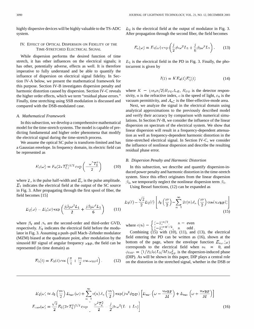
Fig. 15. Block diagram of the differential photonic time-stretched A/D converter. Repetition rate of the optical source isT . One of the outputs is delayed byT=2before it is combined with the other output. Both outputs can now be captured with a single digitizer. MZM: Mach–Zehnder modulator. SC: Supercontinuum.
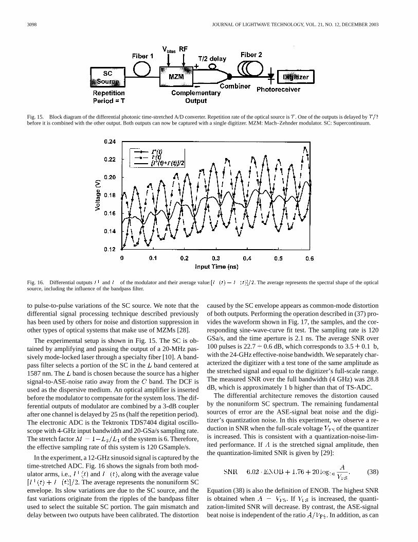
Fig. 16. Differential outputsI andI of the modulator and their average value:[I (t) + I (t)]=2. The average represents the spectral shape of the opticalsource, including the influence of the bandpass filter.
to pulse-to-pulse variations of the SC source. We note that thedifferential signal processing technique described previouslyhas been used by others for noise and distortion suppression inother types of optical systems that make use of MZMs [28].
The experimental setup is shown in Fig. 15. The SC is ob-tained by amplifying and passing the output of a 20-MHz pas-sively mode-locked laser through a specialty fiber [10]. A band-pass filter selects a portion of the SC in theband centered at1587 nm. The band is chosen because the source has a highersignal-to-ASE-noise ratio away from the band. The DCF isused as the dispersive medium. An optical amplifier is insertedbefore the modulator to compensate for the system loss. The dif-ferential outputs of modulator are combined by a 3-dB couplerafter one channel is delayed by 25 ns (half the repetition period).The electronic ADC is the Tektronix TDS7404 digital oscillo-scope with 4-GHz input bandwidth and 20-GSa/s sampling rate.The stretch factor of the system is 6. Therefore,the effective sampling rate of this system is 120 GSample/s.
In the experiment, a 12-GHz sinusoid signal is captured by thetime-stretched ADC. Fig. 16 shows the signals from both mod-ulator arms, i.e., and , along with the average value
. The average represents the nonuniform SCenvelope. Its slow variations are due to the SC source, and thefast variations originate from the ripples of the bandpass filterused to select the suitable SC portion. The gain mismatch anddelay between two outputs have been calibrated. The distortion
caused by the SC envelope appears as common-mode distortionof both outputs. Performing the operation described in (37) pro-vides the waveform shown in Fig. 17, the samples, and the cor-responding sine-wave-curve fit test. The sampling rate is 120GSa/s, and the time aperture is 2.1 ns. The average SNR over100 pulses is 22.7 0.6 dB, which corresponds to 3.50.1 b,with the 24-GHz effective-noise bandwidth. We separately char-acterized the digitizer with a test tone of the same amplitude asthe stretched signal and equal to the digitizer’s full-scale range.The measured SNR over the full bandwidth (4 GHz) was 28.8dB, which is approximately 1 b higher than that of TS-ADC.
The differential architecture removes the distortion causedby the nonuniform SC spectrum. The remaining fundamentalsources of error are the ASE-signal beat noise and the digi-tizer’s quantization noise. In this experiment, we observe a re-duction in SNR when the full-scale voltage of the quantizeris increased. This is consistent with a quantization-noise-lim-ited performance. If is the stretched signal amplitude, thenthe quantization-limited SNR is given by [29]:
(38)
Equation (38) is also the definition of ENOB. The highest SNRis obtained when . If is increased, the quanti-zation-limited SNR will decrease. By contrast, the ASE-signalbeat noise is independent of the ratio . In addition, as can

HAN AND JALALI: PHOTONIC TIME-STRETCHED A/D CONVERTER: FUNDAMENTAL CONCEPTS AND PRACTICAL CONSIDERATIONS 3099
Fig. 17. 120-GSa/s real-time capture of a 12-GHz RF signal by the differential TS-ADC system. The nonuniform envelope is removed by using (37).Effective-noise bandwidth is 24 GHz.
be seen in Fig. 16, due to the nonuniform SC envelope, signalsand could not occupy the full scale of the digitizer
over the entire time aperture. Hence, in the experi-ment, resulting in a reduction in the SNR due to the increaseof the quantization noise. This is the part of reason for the 1-bdifference between the measured ENOB of TS-ADC and theback-to-back experiment. The fact that the SNR is not limited bythe ASE represents an improvement over our previous work [9].This has been achieved by reducing the system losses (hence, areduction in the number of optical amplifiers) and by operatingin the -band portion of the SC where the ASE noise level islower.
The following explanation is necessary with respect to systembandwidth in this particular experiment. In an SSB-modulatedsystem [17], [18], the effective input bandwidth would be
GHz. In the above experiments, because of the unavail-ability of a dual-output SSB modulator, the experiments wereperformed with DSB modulation. The dispersion penalty in thissystem limits the input 3-dB bandwidth to 19.3 GHz. However,for quantization noise and ASE noise, the effective bandwidth is24 GHz, independent of the modulation format (DSB or SSB).
The differential technique is one method for removing the dis-tortion caused by spectral nonuniformities. Another method isfiltering in the digital domain. If the variation caused by distor-tion is slow compared with the RF input signal, it can be sepa-rated from the signal in the frequency domain by low-pass fil-tering. The envelope so obtained can then be used to correct forthe distortion. This method will place a low-frequency cutoffon the system but otherwise is able to compensate the spectralnonuniformity and its pulse-to-pulse dependence. It was em-ployed in the SSB experiment described in Section VI.
The observation that spectral variations are mapped to similarvariations in time (after dispersion) has led us to propose a newmethod for generating ultra wide-band electrical waveformswith arbitrary modulation [30], [31]. In this approach, the spec-trum of a broad-band optical pulse is shaped according to the
Fig. 18. Two adjacent channels of the input signal. By allowing for a finiteoverlap of the two channels, interchannel mismatch errors can be estimated andcorrected.
waveform of interest. Following dispersion, this spectral wave-form is directly transformed into an identical time waveform,which is subsequently converted to electronic domain using aPD. In a recent demonstration, intelligent digital control of thespectrum has been used to render the system insensitive to thenonuniform power spectral density of the optical source [31].The system directly converts digital data to ultra-wide-bandanalog waveforms.
VIII. C ONTINUOUS-TIME OPERATION
To fully understand the operation of the continuous-timetime-stretch ADC, shown in Fig. 2(b), it is instructive to com-pare it with the conventional sample-interleaved ADC shownin Fig. 1. The sample-interleaved approach is the standardapproach for achieving high sampling rate and is used in allsuch electronic digitizers. The input analog signal is simulta-neously applied to a bank on digitizers. Digitizers are thensequentially clocked at a rate of , where is the desiredaggregate sampling rate. The signal is then reconstructed in thedigital domain by combining sequential samples from the arrayof digitizers.
There are two important differences between this architectureand the continuous-time time-stretch system shown in Fig. 2(b).

3100 JOURNAL OF LIGHTWAVE TECHNOLOGY, VOL. 21, NO. 12, DECEMBER 2003
(a)
(b)
Fig. 19. Conceptual block diagrams for two possible implementations of the continuous-time time-stretch ADC. Segmentation is performed (a) using apassivesplitter and time gating and (b) using a passive optical filter.
First is the fact that each digitizer in Fig. 1 sees the input signalat its full bandwidth. Although the requirement on the samplingrate for each digitizer is reduced from to , there is nosuch reduction on the required input bandwidth. Therefore, theinput bandwidth of the system is not improved in this architec-ture. In contrast, the signal is slowed down before it enters thedigitizers in the time-stretched ADC.
The second important difference between the two systemsis the relative (to input frequency) sampling rate of each digi-tizer. In the sample-interleaved system, sampling by each digi-tizer is done at a fraction of the required Nyquist rate. The orig-inal signal can only be recoveredaftersample-by-sample recon-struction in the digital domain. In contrast, because the signalis slowed down prior to digitization, each digitizer samples thesignal at or above the Nyquist rate in the time-stretched ADC. Inother words, a time segment of the input signal is available fromeach digitizerbeforereconstruction. This is a significant featureof the time-stretched ADC and permits real-time cancellation ofmismatch errors, as discussed subsequently.
It is well established that the performance of a sample-in-terleaved ADC is limited by the mismatches between differentchannels [3]. Interchannel gain, offset, and clock skew createspurious tones in the frequency domain and limit the dynamicrange. Owing to its parallel architecture, the time-stretchedADC will also suffer from interchannel mismatch, becausedifferent segments will have to be combined to reconstruct theoriginal signal. However, the fact that sampling in each channelmeets the Nyquist criteria can be used to correct the mismatcherrors. This can be achieved by allowing a finite overlapbetween adjacent segments, as shown in Fig. 18. By comparingsignals from two adjacent digitizers in the overlap region,mismatch errors can be calculated and corrected in the digitaldomain [8]. Because the error is obtained from the signal itself,not from a test signal, one is able to perform real-time errorcorrection, addressing amplitude and frequency dependenciesand dynamic variations of the error. The overhead associatedwith the overlap will decrease with the increase in segmentlength and will not be significant [8].

HAN AND JALALI: PHOTONIC TIME-STRETCHED A/D CONVERTER: FUNDAMENTAL CONCEPTS AND PRACTICAL CONSIDERATIONS 3101
Fig. 20. Physical implementation of the continuous-time time-stretched ADC. The important feature of this design is that signals in all four channels are stretchedin a single fiber, assuring identical stretch factors.
An interesting mode of operation for the continuous-timetime-stretched ADC is one in which reconstruction of the signalfrom different segments is entirely avoided. If the segmentlength is sufficiently long, each segment can provide the neces-sary spectral information. The minimum segment length is thendetermined by the required resolution bandwidth. In this modeof operation, subsequent segments simply update the capturedsignal spectrum at the segment arrival rate. Offset mismatchmanifests itself as uncertainty in the dc component betweeneach segment. Gain mismatch affects the signal amplituderesulting in an uncertainty in the absolute value of the powerspectrum. However, this does not affect the relative power ofthe spectral components, which is the quantity of interest inmost applications. Clock (segment-to-segment timing) skewhas no impact on the resulting spectrum—it will introducea time offset. Since the segment length might not always bean integer multiple of the RF signal period, the segmentationmight introduce errors similar to the leakage errors in digitalsignal processing. However, the error can be minimized withwindowing and/or sufficiently long segments.
A central function in the continuous-time time-stretch ADCis the segmentation of the analog signal into multiple channels.Fig. 19(a) and (b) show block diagrams for two possible ap-proaches to this function. In Fig. 19(a), the signal is split intochannels and then gated prior to the time-stretch block in eachpath. Segmentation is achieved by triggering the switches witha multiphase clock. In Fig. 19(b), the segmentation is performedin a completely passive method using time-to-wavelength map-ping inherent in a chirped optical carrier. The RF signal is firstmodulated onto the chirped optical carrier, in a similar mannerto that shown in Fig. 3. A passive optical filter then performs
wavelength segmentation which, owing to the time-to-wave-length mapping, corresponds to the desired time segmentation.Fig. 20 shows the physical block diagram of a continuous-timetime-stretched ADC, under development in our laboratory. It ex-ploits wavelength–time mapping to perform the segmentationusing passive optical filters. A key design feature of this systemis the use of a single fiber (fiber 2) to stretch all four channels.
IX. CONCLUSION
Time-stretch preprocessing prior to digitization can mitigatemany of the problems that plague ultra-wide-band A/D con-version. Currently, photonics represent the most promising ap-proach to manipulating the time scale of an electrical signal.Since the digitization is performed in the electronic domain,this approach does not compete with electronics; it enhances it.Enhancements include an increase in the sampling rate and theinput bandwidth, reduction in the digitizer sampling jitter noise,and interchannel mismatch errors.
A detailed analytical model that predicts the fidelity of theelectrical output signal has been developed, and its accuracy hasbeen verified by comparing its results with those obtained usingnumerical simulations. The model suggests that the fundamentalperformance improves with a larger optical-to-electrical-band-width ratio. The TBP has been identified as the proper figureof merit for comparing different architectures. With the presenttechnology, TBP is limited to a few hundred when DSB mod-ulation is employed. Because this limit is set by dispersion inthe fiber, one can overcome it with SSB modulation if the re-maining phase distortion can be corrected by an equalization

3102 JOURNAL OF LIGHTWAVE TECHNOLOGY, VOL. 21, NO. 12, DECEMBER 2003
filter in the digital domain. Such a system will become loss-lim-ited, and TBP values of several thousand can be achieved formoderated loss values (see Fig. 11). Assuming the quantizationnoise of the electronic digitizer is sufficiently low, the SNR of anamplified time-stretch system will be limited by the ASE-signalbeat noise. To maximize the SNR, a proper design with optimumamplifier gains and locations and an SC source with high powerspectral density are critical.
An important practical challenge is the nonuniform powerspectral density, and pulse-to-pulse variations of the broad-bandoptical source used for time-to-wavelength transformation. Wehave presented two techniques for overcoming these challenges,both of which rely on a modest amount of signal processing inthe digital domain.
To capture a continuous-time input signal, a multichanneltime-stretch system is required. This architecture overcomes theTBP limitation detailed here. In principle, however, it can sufferfrom interchannel mismatch problems that degrade the perfor-mance of conventional sample-interleaved converters. However,there exists a fundamental difference between a parallel time-stretched array and a sample-interleaved converter array. In thelatter, the signal in each channel is sampled at a fraction of therequired Nyquist rate, whereas in the former, it is sampled at,or above, the Nyquist rate. This permits an effective online cal-ibration of the mismatch errors.
APPENDIX
Here, we describe the derivation for (22)–(24).Using (21), when the distortion is relatively small, the expo-
nential terms in (20) can be written in a linear formas
(A1)
Use (A1) and transform (20) into the time domain. The lowersideband signal can be obtained as
(A2)
In (A2), the second and third terms correspond to thedis-tortion and the limited optical bandwidth, respectively. To fur-ther simplify the derivative term in (A2), the third-order disper-sion term in the envelope is ignored and we obtain
(A3)
Using (A3), it can be proven that
holds. The upper sideband can be similarly handled. Substi-tuting all the results into (14), the photocurrent can be obtained
(A4)
(A5)
(A6)
ACKNOWLEDGMENT
The authors would like to thank Dr. J. Murphy andDr. R. Leheny for their support as well as Prof. H. Fetterman,Dr. A. S. Bhushan, Dr. O. Boyraz, A. Nuruzzaman, and J. Hanfor helpful discussions.
REFERENCES
[1] J. A. Wepman, “Analog-to-digital converters and their applications inradio receivers,”IEEE Commun. Mag., vol. 33, pp. 39–45, May 1995.
[2] R. H. Walden, “Analog-to-digital converter survey and analysis,”IEEEJ. Select. Areas Commun., vol. 17, pp. 539–550, Apr. 1999.
[3] W. C. Black and D. A. Hodges, “Time interleaved converter arrays,”IEEE J. Solid-State Circuits, vol. SC-15, pp. 1022–1029, Dec. 1980.
[4] A. Montijo and K. Rush, “Accuracy in interleaved ADC systems,”Hewlett-Packard J., vol. 44, no. 5, pp. 38–46, Oct. 1993.
[5] W. J. Caputi, “Stretch: A time-transformation technique,”IEEE Trans.Aerosp. Electron. Syst., vol. AES-7, pp. 269–278, Mar. 1971.
[6] B. Jalali and F. Coppinger, “Data conversion using time manipulation,”U.S. Patent 6 288 659, Sept. 11, 2001.
[7] F. Coppinger, A. S. Bhushan, and B. Jalali, “Photonic time stretch andits application to analog-to-digital conversion,”IEEE Trans. MicrowaveTheory Tech., vol. 47, pp. 1309–1314, July 1999.
[8] Y. Han, B. Rezaei, V. P. Roychowdhury, and B. Jalali, “Adaptive on-line calibration in time stretched ADC arrays,” inProc. InstrumentationMeasurement Technology Conf., vol. 2, 2003, pp. 1212–1216.
[9] A. S. Bhushan, P. V. Kelkar, B. Jalali, O. Boyraz, and M. Islam,“130 GSa/s photonic analog-to-digital converter with time stretchpreprocessor,”IEEE Photon. Technol. Lett., vol. 14, pp. 684–686, May2002.
[10] O. Boyraz, J. Kim, M. N. Islam, F. Coppinger, and B. Jalali, “Broadband,high-brightness 10-Gbit/s supercontinuum source for A/D conversion,”in Proc. Lasers Electro-Optics Conf., 2000, pp. 489–490.
[11] B. H. Kolner and M. Nazarathy, “Temporal imaging with a time lens,”Opt. Lett., vol. 14, no. 12, pp. 630–632, June 1989.
[12] B. Asuri, Y. Han, and B. Jalali, “Time-stretched ADC arrays,”IEEETrans. Circuits Syst. II, vol. 49, pp. 521–524, July 2002.
[13] E. I. Ackerman and C. H. Cox, “RF fiber-optic link performance,”IEEEMicrowave, vol. 2, pp. 50–58, Dec. 2001.
[14] R. Ramaswami and K. N. Sivarajan,Optical Networks, 2nd ed. SanMateo, CA: Morgan Kaufmann, 2002.
[15] G. P. Agrawal,Nonlinear Fiber Optics, 3rd ed. San Diego, CA: Aca-demic, 2001, ch. 3.
[16] H. Schmuck, “Comparison of optical millimeter-wave system conceptswith regard to chromatic dispersion,”Electron. Lett., vol. 31, no. 21, pp.1848–1849, Oct. 1995.
[17] J. M. Fuster, D. Novak, A. Nirmalathas, and J. Marti, “Single-sidebandmodulation in photonic time-stretch analogue-to-digital conversion,”Electron. Lett., vol. 37, no. 1, pp. 67–68, Jan. 2001.

HAN AND JALALI: PHOTONIC TIME-STRETCHED A/D CONVERTER: FUNDAMENTAL CONCEPTS AND PRACTICAL CONSIDERATIONS 3103
[18] Y. Han and B. Jalali, “Time-bandwidth product of the photonic time-stretched analog-to-digital converter,”IEEE Trans. Microwave TheoryTech., vol. 51, pp. 1886–1892, July 2003.
[19] A. Hilt, “Microwave harmonic generation in fiber-optical links,” inProc.13th Int. Conf. Microwaves, Radar Wireless Communications, vol. 2,2000, pp. 693–698.
[20] G. H. Smith, D. Novak, and Z. Ahmed, “Technique for optical SSB gen-eration to overcome dispersion penalties in fiber-radio systems,”Elec-tron. Lett., vol. 33, no. 1, pp. 74–75, Jan. 1997.
[21] S. Dubovitsky, W. H. Steier, S. Yegnanarayanan, and B. Jalali, “Analysisand improvement of Mach–Zehnder modulator linearity performancefor chirped and tunable optical carriers,”J. Lightwave Technol., vol. 20,pp. 886–891, May 2002.
[22] K. Yonenaga and N. Takachio, “A fiber chromatic dispersion compen-sation technique with an optical SSB transmission in optical homodynedetection systems,”IEEE Photon. Technol. Lett., vol. 5, pp. 949–951,Aug. 1993.
[23] J. Park, W. V. Sorin, and K. Y. Lau, “Elimination of the fiber chromaticdispersion penalty on 1550 nm millimeter-wave optical transmission,”Electron. Lett., vol. 33, no. 6, pp. 512–513, Mar. 1997.
[24] K. Chang, I. Bahl, and V. Nair,RF and Microwave Circuit and Compo-nent Design for Wireless Systems. New York: Wiley, 2002.
[25] M. Nakazawa, K. Tamura, H. Kubota, and E. Yoshida, “Coherencedegradation in the process of supercontinuum generation in an opticalfiber,” Optical Fiber Technology, vol. 4, no. 2, pp. 215–223, 1998.
[26] O. Boyraz, J. Kim, M. N. Islam, F. Coppinger, and B. Jalali, “10 Gb/smultiple wavelength, coherent short pulse source based on spectralcarving of supercontinuum generated in fibers,”J. Lightwave Technol.,vol. 18, pp. 2167–2175, Dec. 2000.
[27] Y. Han and B. Jalali, “Differential photonic time stretch analog-to-digitalconverter,” presented at the Lasers and Electro-Optics Conf., Baltimore,MD, June 1–6, 2003, Paper CWH2.
[28] J. C. Twichell and R. Helkey, “Phase-encoded optical sampling foranalog-to-digital converters,”IEEE Photon. Technol. Lett., vol. 12, pp.1237–1239, Sept. 2000.
[29] J. G. Proakis and D. G. Manolakis,Digital Signal Processing: Prin-ciples, Algorithms, and Applications, 3rd ed. Englewood Cliffs, NJ:Prentice-Hall, 1996.
[30] B. Jalali, P. Kelkar, and V. Saxena, “Photonic arbitrary waveform gener-ator,” in Proc. 14th Annu. Meeting IEEE Lasers Electro-Optics Society,vol. 1, 2001, pp. 253–254.
[31] J. Chou, Y. Han, and B. Jalali, “Adaptive RF-photonic arbitrarywaveform generator,” inProc. Microwave Photonics Conf., 2002, PaperT2–1, pp. 93–96.
Yan Han received the B.S. and M.S. degrees inelectronic engineering from the Tsinghua University,Beijing, China, in 1998 and 2000, respectively. Heis currently working toward the Ph.D. degree withthe Department of Electrical Engineering at theUniversity of California, Los Angeles (UCLA).
His research interests include the areas of mi-crowave photonics, optical communications, opticalamplifiers, and fiber optics.
Bahram Jalali (S’86–M’89–SM’97–F’03) was aMember of Technical Staff at the Physics ResearchDivision of AT&T Bell Laboratories, Murray Hill,NJ, from 1988 to 1992, where he conducted researchon ultrafast electronics and optoelectronics. In 1992,he was responsible for successful development anddelivery of 10-Gb/s lightwave circuits to the U.S.Air Force. He is currently a Professor of ElectricalEngineering, the Director of the DARPA Center forOptical A/D System Technology (COAST), and theDirector of the Optoelectronic Circuits and System
Laboratory at the Universeity of California, Los Angeles (UCLA). While onleave from UCLA between 1999 and 2001, he founded Cognet Microsystems,a Los Angeles, CA-based fiber-optic component company that was acquiredby Intel Corporation in 2001. He has more than 120 publications and holds fiveU.S. patents. He currently serves as a Consultant for the Wireless NetworkingGroup (WNG) of Intel Corporation. His current research interests are inmicrowave photonics, integrated optics, and fiber-optic integrated circuits.
Dr. Jalali is a Member of the California Nano Sciences Institute (CNSI) andis the Chair of the Los Angeles Chapter of the IEEE Lasers & Electro-OpticsSociety (LEOS). He was the General Chair for the IEEE international confer-ence on Microwave Photonics (MWP) in 2001 and its Steering Committee chairfrom 2001–present, and he serves on the Board of Trustees of the California Sci-ence Center. He received the BridgeGate 20 Award in 2001 in recognition of hiscontributions to the Southern California hi-tech economy.


![Broadband SOI mode order converter based on topology ... · 1 converter by topology optimization [2] is designed in photonic crystal operation regime with a narrow bandgap, which](https://img.dokumen.tips/doc/110x75/5f2f2e836dd4801ba82eb4d6/broadband-soi-mode-order-converter-based-on-topology-1-converter-by-topology.jpg)