Embed Size (px)
Citation preview
Photonic Integrated Circuits Using III-V Nanopillars Grownon Silicon
Wai Son Ko
Electrical Engineering and Computer SciencesUniversity of California at Berkeley
Technical Report No. UCB/EECS-2016-172http://www2.eecs.berkeley.edu/Pubs/TechRpts/2016/EECS-2016-172.html
December 1, 2016

Copyright © 2016, by the author(s).All rights reserved.
Permission to make digital or hard copies of all or part of this work forpersonal or classroom use is granted without fee provided that copies arenot made or distributed for profit or commercial advantage and that copiesbear this notice and the full citation on the first page. To copy otherwise, torepublish, to post on servers or to redistribute to lists, requires priorspecific permission.
Photonic Integrated Circuits Using III-V Nanopillars Grown on Silicon
by
Wai Son Ko
A dissertation submitted in partial satisfaction of the
requirements for the degree of
Doctor of Philosophy
in
Engineering – Electrical Engineering and Computer Sciences
and the Designated Emphasis
in
Nanoscale Science and Engineering
in the
Graduate Division
of the
University of California, Berkeley
Committee in charge:
Professor Connie J. Chang-Hasnain
Professor Ming C. Wu
Professor Oscar Dubon
Fall 2014

Nanopillar Photonic Integrated Circuits Built on Silicon
Copyright © 2014
by
Wai Son Ko
1
Abstract
Photonic Integrated Circuits Using III-V Nanopillars Grown on Silicon
by
Wai Son Ko
Doctor of Philosophy in Engineering – Electrical Engineering and Computer Sciences
And the Designated Emphasis in Nanoscale Science and Engineering
University of California, Berkeley
Professor Connie J. Chang-Hasnain, Chair
Advancement in transistor scaling and integration technology has given electronics tremendous
amount of computational power. Yet, extending integration to include photonics can augment
computation with the ability to create and manipulate light. Such tight electronic-photonic
integration can create exciting new opportunities, such as high speed, low energy on-chip optical
interconnects, advanced optical sensors, and other unforeseen applications.
Electronic-photonic integration using traditional integration methods happens to be a difficult task,
however. Photonic components, such as lasers and light emitting diodes, are typically made with
III-V semiconductors since silicon, the material that electronics are built on, lacks light generation
ability due to its indirect band gap. Simply combining III-V materials with silicon using
conventional thin film growth technique often results in nonfunctional or subpar devices because
the lattice spacing mismatch between III-V and silicon creates performance degrading defects.
This problem, nevertheless, can be mitigated with nanostructure growth. Thanks to the nanoscale
footprint, strain from lattice mismatch can fully relax, allowing monolithic integration of high
quality III-V materials onto silicon as building blocks for high performance optoelectronic devices.
In this dissertation, a variety of optoelectronic devices integrated onto silicon using InGaAs and
InP nanopillars will be presented. High speed nano light emitting diode (nano-LED) capable of
generating stimulated emission is demonstrated. Observing stimulated emission from such a nano-
LED marks a great milestone towards realizing electrically driven laser on silicon. And when the
nano-LED is under reverse bias, the device acts as a highly efficient avalanche photodiode yielding
100x gain at as little as 1 V reverse bias. Under solar illumination, the device shows angle
insensitive response and high photovoltaic efficiency of 19.6%, the highest ever reported for an
InP nanostructure solar cell grown on low cost silicon substrate. Furthermore, a more sophisticated,
highly sensitive bipolar junction phototransistor is made on silicon as an integrated detector to
enable low energy photonic interface to logic circuit. And to validate nanopillar as viable means
to building photonic integrated circuit, a proof of concept photonic data link is built and
demonstrated on silicon. With nanopillar optoelectronics, tight electronic-photonic integration is
becoming a reality, opening the door to a new generation of convergent electronic devices with
far-reaching photonic capabilities.

To my beloved family

i
Table of Contents
Table of Contents ...........................................................................................................................1
List of Figures .................................................................................................................................3
Acknowledgement ........................................................................................................................11
Chapter 1 Introduction..................................................................................................................1
Chapter 2 III-V Integration with Silicon .....................................................................................4
2.1 Growth of (In)GaAs Nanopillars ............................................................................................7
2.2 Growth of InP Nanopillars ...................................................................................................15
Chapter 3 Site Control Growth of Nanopillars .........................................................................17
3.1 Site Controlled Growth of InGaAs Nanopillars ...................................................................17
3.2 Site Controlled Growth of InP Nanopillars ..........................................................................21
Chapter 4 Resonant Nanopillar Light Emitting Diode ............................................................28
4.1 Introduction to Electrically Driven Nano Light Emitters .....................................................28
4.2 Fabricating Nanopillar into Electrical Device ......................................................................29
4.3 InGaAs Nanopillar Diode Electroluminescence ..................................................................33
4.4 High Speed Operation of Nanopillar LED ...........................................................................35
4.5 Towards Nanolaser on Silicon .............................................................................................36
4.6 Silicon Transparent Emission ...............................................................................................39
Chapter 5 Nanopillar Avalanche Photodiode............................................................................42
5.1 The Need for Ultra-Sensitive Detector .................................................................................42
5.2 Huge Current Gain at Small Bias Voltage ...........................................................................44
5.3 Low Voltage GaAs Nanoneedle Avalanche Photodiodes ....................................................47
5.4 Low Voltage InGaAs Nanopillar Avalanche Photodiodes ..................................................51
5.5 Giant Gain from InP Photodiodes ........................................................................................52
Chapter 6 Nanopillar Phototransistor .......................................................................................57
6.1 Phototransistor to Reduce Energy/Bit Further .....................................................................57
6.2 Nanopillar Phototransistor Design and Operation ...............................................................58
6.3 Regrowth on InP Nanopillar – Achieving Record Low Dark Current in Nanowire
Devices .................................................................................................................................60
6.4 Bipolar Junction Phototransistor in Action ..........................................................................64

ii
Chapter 7 Illumination Angle Insensitive, High Efficiency Solar Cell using Single
Indium Phosphide Nanopillar ..................................................................................66
7.1 Introduction to Nanowire/Nanopillar Solar Cells ................................................................66
7.2 Material Growth and Fabrication .........................................................................................67
7.3 Photovoltaic Performance ....................................................................................................68
7.4 Temperature Dependence .....................................................................................................69
7.5 External Quantum Efficiency ...............................................................................................70
7.6 Dielectric Antenna Effect and Angle Insensitivity ..............................................................73
Chapter 8 On-Chip Optical Data Link ......................................................................................76
8.1 Interconnecting Nanopillars with Waveguides ....................................................................76
8.2 Optical Link Operation .........................................................................................................78
Chapter 9 Conclusion ..................................................................................................................80
References .....................................................................................................................................82

iii
List of Figures
Figure 2.1 Elastic strain relaxation in III-V nanostructures grown on silicon. a, Strain
from lattice mismatch causes dislocations in thin film growth. b, The small footprints of
nanostructures allow elastic strain relaxation despite the large lattice mismatch. ..................... 5
Figure 2.2 Poor optical mode overlap with conventional nanowires that are subjected to
the critical diameter of < 300 nm. ........................................................................................... 6
Figure 2.3 As grown InGaAs nanopillars passivated with in situ GaAs shell. ....................... 7
Figure 2.4 Growth of nanopillar. From nanocluster to layer-by-layer core-shell growth to
nanopillar. An in situ surface passivation layer can be added as well. ..................................... 7
Figure 2.5 Core-shell growth of nanopillar. The nanopillar starts as a nanocluster, and
grow bigger and bigger in a core-shell manner. ......................................................................... 8
Figure 2.6 Transmission electron microscope images confirm the tiny root of InGaAs
nanopillars. a, Schematic of the InGaAs nanopillar lamella shown in b. b, Transmission
electron micrograph image of a thin slice of an InGaAs nanopillar. c, High magnification
image of the root of the nanopillar in b. d, High resolution transmission electron
microscope image of the body of the nanopillar in b, showing the single crystalline wurtzite
structure of the nanopillar. ......................................................................................................... 9
Figure 2.7 Size scaling with growth time. ................................................................................ 10
Figure 2.8 Controlling the size of GaAs nanoneedles. 30° tilt SEM images of (a) a GaAs
nanoneedle grown continuously for 30 min at 395°C, (b) half-length GaAs nanopillars
achieved by stopping group-III precursor flow for 1 min after a 15 min growth, followed
by another 15 min growth, and (c) a GaAs nanoneedle grown with a 1 min pause of group-
V precursor after a 15 min growth, followed by another 15 min growth. For all three cases,
the diameters are the same at ~ 300 nm. d, Average lengths and diameter growth rates for
GaAs nanoneedles grown for 30 min under various growth conditions. The growth
condition changes that stop the [0001] growth happened 15 min into the growth. ................ 11
Figure 2.9 Controlling the size of InGaAs nanoneedles. 30° tilt SEM images of (a) An
InGaAs nanoneedle grown continuously for 30 min at 400°C, (b) InGaAs nanoneedles with
random lengths grown by introducing a 2 min 425°C thermal shock between a 10 min and
20 min growth, and (c) one-third height InGaAs nanopillars were acheived by introducing
a 2 min 450°C thermal shock between a 10 min and 20 min growth. For all three cases,
the diameters are all the same at ~ 300 nm. d, Average lengths and diameter growth rates
for InGaAs nanoneedles grown for 30 min under various growth conditions. The growth
condition changes that stop the [0001] growth happened 15 min into the growth. ................ 12
Figure 2.10 [𝟏𝟐𝟏𝟎] zone axis high resolution transmission electron microscope images
of the tip of length controlled nanopillars. Zinc-blende lattice structure can be seen at
the tip of the GaAs (a) and InGaAs (b) nanopillars that had the growth in the [0001] direction stopped via growth condition change. ...................................................................... 12

iv
Figure 2.11 Nanopillar laser grown on silicon. a, Lasing spectra of as grown nanopillar.
b, Light input versus light output curve (L-L) of the lasing nanopillar showing the
characteristic S shaped dependence. ........................................................................................ 13
Figure 2.12 Nanopillars grown on MOSFETs. a, A schematic showing nanopillars
growing on anywhere there is silicon. b, A scanning electron micrograph showing a
nanopillar grown on the gate of a MOSFET. c, A scanning electron micrograph showing
a nanopillar grown on the source of a MOSFET. .................................................................... 14
Figure 2.13 Laser characteristics for a nanopillar grown on a MOSFET. a, L-L curve
showing a laser characteristic S-shape dependence. b, Lasing spectrum of the nanopillar
showing the narrow linewidth. ................................................................................................. 14
Figure 2.14 MOSFET performance remains unchanged after nanopillar growth. a,
Transistor transfer characteristic before and after growth. b, Transistor output
characteristic also remains unchanged. .................................................................................... 15
Figure 2.15 Growth evolution of InP nanopillars (courtesy of Fan Ren of reference [51]).
Core-shell growth allows the size of InP nanopillars to scale with growth time. .................... 15
Figure 2.16 Transmission electron microscope studies show the single crystalline quality
of InP nanopillars (from reference [51]). a, High resolution transmission electron
microscope image showing the wurtzite crystal structure of an InP nanopillar. b,
Diffraction pattern of a showing the perfect wurtzite crystal diffraction pattern. ................... 16
Figure 2.17 Lasing from as grown InP nanopillars (from reference [51]). a, Lasing
spectrum of an InP nanopillar. b, S shaped light input versus light output curve from the
InP nanolaser in a. .................................................................................................................... 16
Figure 3.1 Processing steps to prepare for selective area growth. a, Thermal oxidation to
create growth control mask on silicon substrate. b, Deep ultra-violet lithography is used
to create hole patterns on the growth mask. c, Nanopillar growth takes place only at the
mask openings. ......................................................................................................................... 17
Figure 3.2 Atomic force microscope image of fabricated silicon dioxide site control mask. The holes here are 400 nm in diameter and spaced 800 nm apart. The image is scaled so
that the holes are at a height of 0 nm. ...................................................................................... 18
Figure 3.3 Site controlled growth of In0.2Ga0.8As nanopillars. a, Scanning electron
microscope image showing the regular array of nanopillars. b, Zoomed in scanning
electron microscope image taken at 30° angle. c, Scanning electron microscope image
taken from the top. ................................................................................................................... 19
Figure 3.4 Increasing nucleation of site controlled growth by decreasing indium
precursor flow. This scanning electron micrograph shows that every single hole has
nucleation when indium precursor flow is reduced from 7 sccm to 4 sccm. ........................... 20
Figure 3.5 Influence of hole dimension on InGaAs nanopillar nucleation. The top-view
scanning electron microscope images above show site controlled nanopillars after just five
minutes of growth. When the holes are too small (< 60 nm diameter), nanopillars do not
nucleate. But when the wholes are too big (> 90 nm diameter), multiple nanopillars start
to nucleate from the same hole. ............................................................................................... 20
v
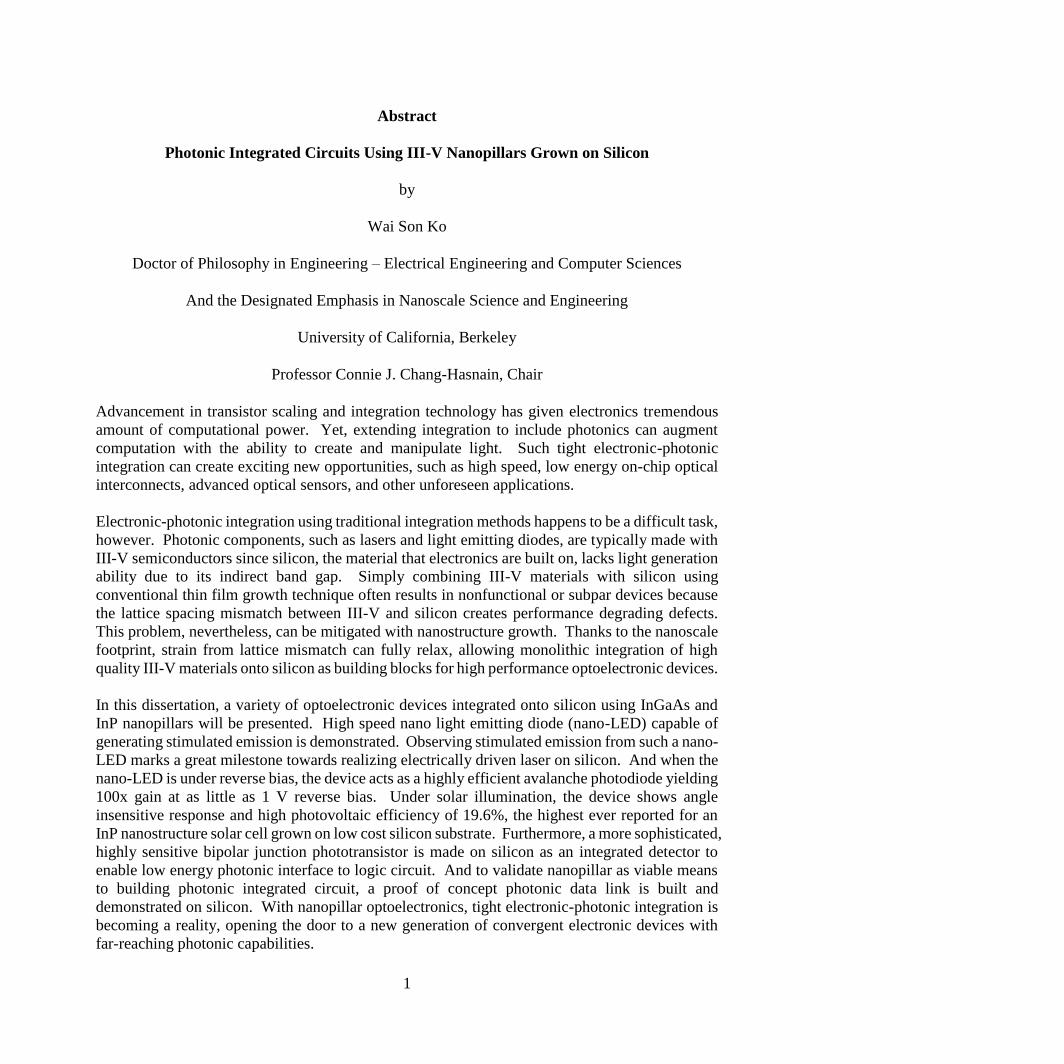
Figure 3.6 Lasing characteristics of site controlled InGaAs nanopillar. a, Lasing
emission from a site controlled InGaAs nanopillar. The inset shows the microscope image
of the speckle pattern observed when the nanopillar is lasing. b, A clear threshold of 40
µJ/cm2 pumping fluence can be seen on the light output as a function of pump fluence
curve (L-L curve). .................................................................................................................... 21
Figure 3.7 Site controlled growth of InP nanopillars. a, Scanning electron micrograph
image of InP nanopillars in a regular array. The holes are 380 nm wide and spaced 10 µm
apart. b, Close-up view of InP nanopillars grown in an array of holes that are 380 nm wide
and spaced 6 µm apart. ............................................................................................................. 22
Figure 3.8 Influence of hole diameter on site controlled growth of InP nanopillars. When
the holes are too small, the percentage of holes filled drops. .................................................. 23
Figure 3.9 Influence of hole spacing on site controlled growth of InP nanopillars. Optimal hole spacing is found to be between 3 – 10 µm. ........................................................ 24
Figure 3.10 Varying V/III ratio to improve yield of InP nanopillar site controlled growth. But yield is found to be quite near optimum at standard growth condition. At -20% and
+20% of standard V/III ratio for InP nanopillar growth, yield for site controlled growth
drops significantly. ................................................................................................................... 25
Figure 3.11 Transmission electron microscope images of an InP nanopillar grown with
site controlled growth. The images show that the nanopillar base completely fills the hole
used for site control, and it makes direct contact to the silicon substrate. The nanopillar
also has excellent material quality with only a few stacking faults running horizontally, but
largely confined to the base of the nanopillar. ......................................................................... 26
Figure 3.12 Site controlled growth provides natural electrical isolation for p-n junctions. Here, the n-doped shell is electrically isolated from the silicon substrate because of the
overgrowth and silicon dioxide mask used for site controlled growth. ................................... 27
Figure 4.1 InGaAs Nanopillar and LED devices. a, 60° tilt SEM image of as-grown
nanopillar with radial p-i-n layers. b, 45° tilt SEM image of a fabricated LED device. c,
Schematic illustrating a nanopillar device embedded inside a metal cavity as a step toward
electrically driven diode laser on silicon. ................................................................................. 29
Figure 4.2 Scanning electron image of a nanopillar sample with alignment marks laid
down to help locate the position of the nanopillars. The exact position of the nanopillars
can be computed by triangulating from the known positions of the alignment marks. ........... 30
Figure 4.3 Process flow of nanopillar device. a, Nanopillar structure after growth. The red
arrow denotes the current leakage path to be eliminated during fabrication. b, Alignment
marks are laid down just after growth using electron beam lithography to help locate the
nanopillars. c, Alignment marks metal evaporation and nanopillar location registration. d,
Silicon dioxide, which is later used as an etch mask, is deposited everywhere via plasma
enhanced chemical vapor deposition. e, Electron beam lithography is used to define an
etch mask that is the size of the nanopillar. f, Unwanted silicon dioxide is etched away in
buffered hydrofluoric acid, leaving a silicon dioxide etch mask over the nanopillar. g,
Polycrystalline layer that is deposited during growth is etched away by dry etching in
silicon tetrachloride. The p-doped shell of the nanopillar is also wet etched away in piranha.
h, A second layer of silicon dioxide is deposited via plasma enhanced chemical vapor
vi
deposition. This silicon dioxide layer electrically isolates the substrate from the top contact
metal that is to be deposited. i, j, A photoresist etch back process is used to expose the tip
of the nanopillar. k, Electron beam lithography to define contact to individual nanopillar.
l, Metal is deposited to both top and bottom of the wafer to complete the fabrication............ 32
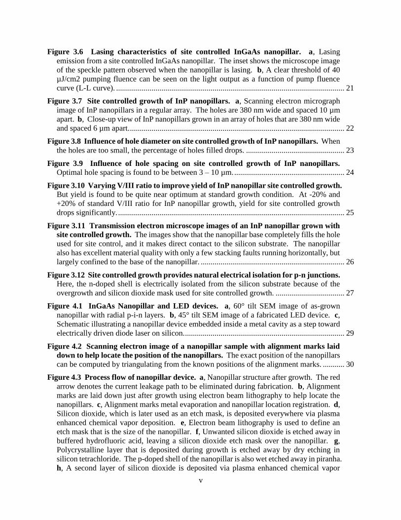
Figure 4.4 Device characteristics of a nanopillar LED. a, IV curve of a typical nanopillar
LED. Dark current is low at 150 fA and 2 nA at 0 V and -1 V, respectively. The ideality
factor is near ideal at ~ 2.3. b, Electroluminescence spectra of a nanopillar LED showing
prominent stimulated emission peak under continuous wave current injection at 4 K. The
inset shows an optical image of the stimulated emission with an apparent mode pattern. c,
Linewidth of nanopillar LED. .................................................................................................. 34
Figure 4.5 Temperature and polarization dependence data of a LED device. a, The
temperature dependence spectra show red shifting of the emission wavelengths as
temperature is increased. When the smaller sub peaks (highlighted by colored arrows) and
the overall spontaneous emissions are fitted and plotted against temperature as shown in
the inset, the sub peaks are revealed to shift at a slower rate than the spontaneous emission
peaks. In fact, the sub peaks shift at a rate expected for the refractive index, while the
spontaneous emission peaks shift according to the Varshni model for band gap energies.
For this experiment, 20 ns current pulses were used to minimize heating effects. b,
Although the photoluminescence of an as-grown nanopillar (black) shows no polarization
dependence, the LED emission at 1.1 µm in Figure 4.4b shows large polarization
dependence (red). The grey hexagon in the center depicts the crystal orientation of the
nanopillar.................................................................................................................................. 35
Figure 4.6 High speed measurement of nanopillar LED. a, Time resolved emission of a
LED when excited with 80 ns pulse. The rise time and fall time of the LED is found to be
140 ps and 300 ps, respectively. This suggests that the nanopillar LED is capable of > 1
GHz operation. b, Direct modulation of a nanopillar LED at 2.5 GHz. ................................. 36
Figure 4.7 Carrier lifetime measurement of InP nanopillars (courtesy of Kun Li of
reference [85]). The data shows a fast radiative recombination lifetime of around 300 ps
at 4 K, and a lack of measurable non-radiative recombination. ............................................... 37
Figure 4.8 Evidence of indium composition inhomogeneity in InGaAs nanopillars. a,
Broad emission spectrum (~ 400 nm) is usually observed from InGaAs nanopillar
electroluminescence. b, SEM image of an In0.2Ga0.8As nanopillar (capped with 120 nm of
GaAs) after being etched in C6H8O7:H2O2 in 2:1 ratio. The image shows a hexagonal pizza
pattern that is left behind at the core of the nanopillar. Since this acid etches indium rich
InGaAs faster, the result indicates a lack of indium concentration uniformity at the core of
the InGaAs nanopillar. This indium inhomogeneity contributes to the broad
electroluminescence spectrum observed in (a). ....................................................................... 38
Figure 4.9 Schematic and sketch showing how improved cavity design may lead to
electrically driven lasing in nanopillars on silicon. a, Schematic pointing out the silicon
dioxide spacer. b, Sketch showing the tradeoff between optical confinement and metal
absorption loss as the silicon dioxide spacer thickness is changed. ......................................... 39
Figure 4.10 Electroluminescence of an InGaAs nanopillar LED with silicon transparent
emission. InGaAs nanopillars typically emits at 900 – 1100 nm. But due to indium

vii
composition incorporation fluctuation, the emission from this nanopillar peaks at 1.35 µm.
There is also no detectable emission below 1.2 µm for this nanopillar. .................................. 39
Figure 4.11 InP nanopillar with an InGaAs layer grown within the body (from reference
[51]). a, Schematic of an InP nanopillar with InGaAs layer grown inside. b, SEM image
of an InP nanopillar with InGaAs layer grown inside. c, Cross-section SEM image of an
InP nanopillar with InGaAs inner layer after it has been etched with an etchant that
selectively etches away InGaAs. The etched InGaAs layer shows that there is indeed an
InGaAs layer within the InP nanopillar. .................................................................................. 40
Figure 5.1 Schematic of an optical interconnect. .................................................................... 43
Figure 5.2 Band diagram illustrating impact ionization. Under low electric field, carriers
that undergo collision lose their energy through thermalization. But under high electric
field, carriers undergoing collision may have enough energy to cause bound carriers to
become unbound. These newly created carriers may undertake the same process to create
more free carriers, creating what is known as avalanche breakdown in a diode. .................... 44
Figure 5.3 GaAs nanopillar APD device structure used in Sentaurus device simulation
to study the electric field concentration effect inside a curved p-n junction. ................... 46
Figure 5.4 Electric field distribution inside a GaAs nanopillar photodiode at 8 V reverse
bias. Regions with electric field beyond the critical field (4.5 × 10⁵ V/cm) for impact
ionization can be clearly seen. With impact ionization, carrier multiplication gives rise to
avalanche gain in photocurrent. ............................................................................................... 46
Figure 5.5 Fabrication process flow for GaAs avalanche photodiodes. a, Growth of GaAs
nanoneedles with built-in core-shell p-n junctions. b, Photoresist etch-back process to
expose the tips of nanoneedles. c, Gold evaporation at 30° angle to serve as an etch mask
to half of the p-type GaAs shell. d, Part of the p-GaAs shell is removed in piranha to
prevent leakage current from the p-GaAs shell to the substrate. e, Spin-on-glass is spun on
to planarize the sample and to insulate the n-GaAs core. f, Contact pads are defined using
conventional contact photolithography. Then, metal is evaporated at 30° to form the p-
type contact. N-type contact is established through the backside of the silicon substrate. ..... 47
Figure 5.6 SEM image of a fabricated GaAs APD device. ..................................................... 48
Figure 5.7 GaAs nanopillar APD device performance. a, Current-voltage (IV)
characteristics of a GaAs nanopillar APD tested under dark and illuminated condition. The
photocurrent of the device increases as bias voltage increases, which is a sign of gain in
the device. b, Lower bound multiplication factor for device shown in (a). ............................ 49
Figure 5.8 Photocurrent measured when the laser spot is moved away from the
nanoneedles. The photocurrent measured shows an exponential drop off as the
illumination distance is moved away from the nanoneedles. The photodiode is biased at -
10 V throughout this measurement. This measurement is also taken with a 980 nm laser
spot, which is below the band gap of the GaAs nanoneedle. So any photocurrent measured
comes from absorption in the silicon substrate. ....................................................................... 50
Figure 5.9 A schematic (a) and a scanning electron micrograph (b) of an avalanche
photodiode made with a single InGaAs nanopillar. Only one side of the nanopillar is
coated with metal, leaving the other side exposed for light detection. .................................... 51
viii
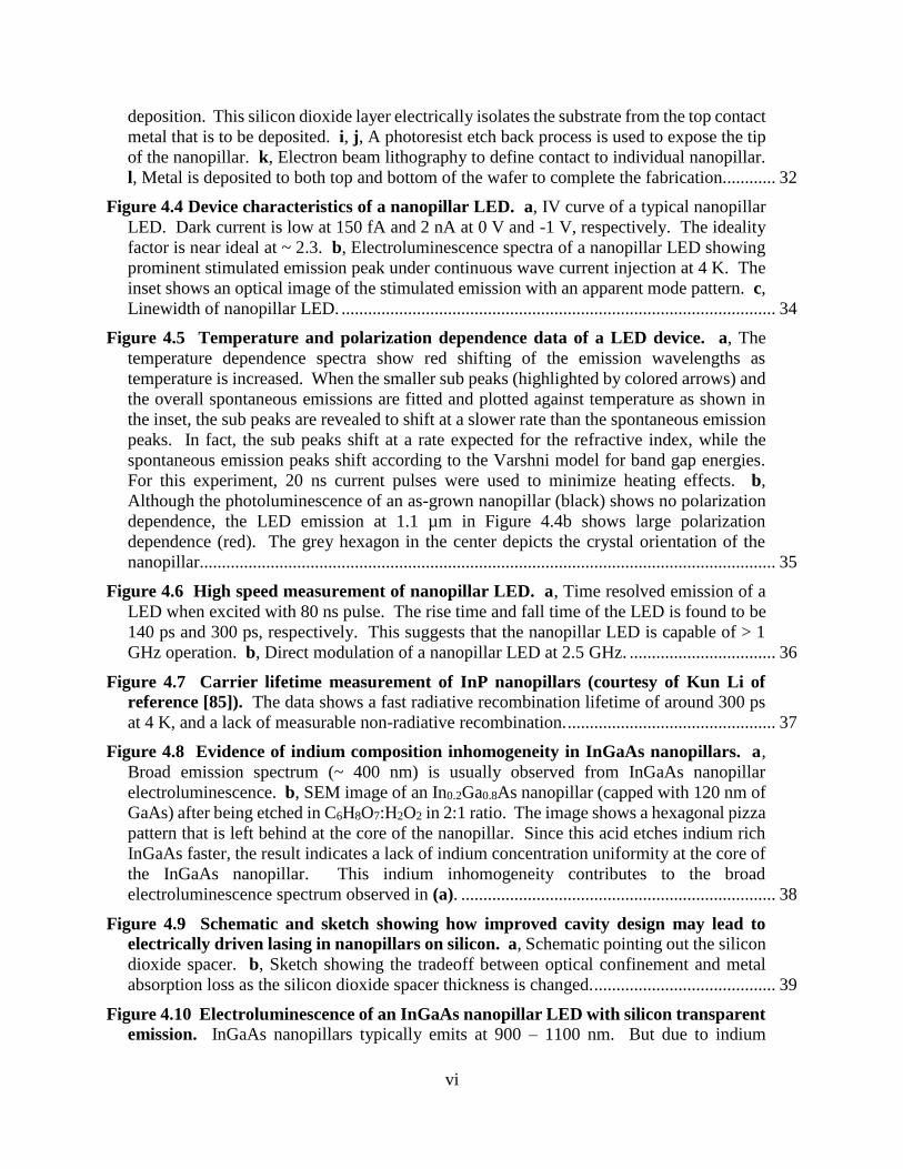
Figure 5.10 InGaAs nanopillar avalanche photodiode device characteristics. a, Current-
voltage (IV) behavior. b, Photocurrent and gain of the device. .............................................. 52
Figure 5.11 Frequency response of InGaAs avalanche photodiode. The device has a 3 dB
bandwidth of 3.1 GHz. ............................................................................................................. 52
Figure 5.12 Fabrication process for InP nanopillar devices. a, Nanopillar structure after
growth. b, Alignment marks are laid down just after growth using electron beam
lithography to help locate the nanopillars. c, Alignment marks metal evaporation and
nanopillar location registration. d, Silicon dioxide is deposited via plasma enhanced
chemical vapor deposition. This silicon dioxide layer electrically isolates the substrate
from the top contact metal that is to be deposited. e, f, A photoresist etch back process is
used to expose the tip of the nanopillar. g, Electron beam lithography to define contact to
individual nanopillar. h, Metal is deposited to both top and bottom of the wafer to complete
the fabrication........................................................................................................................... 53
Figure 5.13 Schematic (a) and SEM (b) of InP nanopillar avalanche photodiode. ............. 54
Figure 5.14 InP nanopillar avalanche photodiode device characteristics. a, IV curves of
InP nanowire APD under dark and 1.6 nW laser excitation at 660 nm wavelength. b,
Photocurrent/gain as a function of bias voltage for the APD. With just 1 V bias, the InP
nanowire APD is able to reach a gain of 100. .......................................................................... 55
Figure 5.15 InP nanopillar avalanche photodiode shows no photocurrent when the laser
spot is moved away from the center of the nanopillar device. In fact, the photocurrent
drops off to 0 A as soon as the laser spot is moved 3 µm away, which is consistent with a
5 µm laser spot size. The schematic on the right shows how the distance in the plot on the
right is defined.......................................................................................................................... 56
Figure 6.1 Schematics and scanning electron micrograph of single InP nanopillar
bipolar junction phototransistor fabricated on silicon substrate. a, 3-D schematic of
the device. b, Cross-section schematic. The device consists of p-doped emitter outer shell,
n-doped base in the middle, and p-doped collector core. c, Scanning electron micrograph
of a fabricated device. .............................................................................................................. 58
Figure 6.2 Band structure inside a bipolar junction phototransistor. a, Band diagram of
a bipolar junction phototransistor without light illumination, but under a slight emitter-
collector bias. b, Band diagram of a bipolar junction phototransistor under light
illumination. Under illumination, electrons (blue dots) accumulate at the base, causing a
rise in the Fermi energy with the base. This effectively lowers the potential barrier so that
thermally excited holes can get injected into the base more easily. Most of these injected
holes end up making across to the collector side, thus, increasing the collector current. c,
Schematic illustrating the emitter-collector bias. ..................................................................... 59
Figure 6.3 The problem without regrowth. Schematic showing the problem of shunt
current path when the layers of a bipolar junction phototransistor is grown in one
continuous growth. Since the p-doped emitter is touching the p-doped silicon substrate
directly, current always flows between the emitter and collector contacts. ............................. 61
Figure 6.4 Regrowth on nanopillar. Schematics of a nanopillar before and after regrowth. .. 62
ix
Figure 6.5 Regrowth on nanopillar. a, Scanning electron micrographs of a nanopillar
before and after the regrowth. The regrown layers only grow on the top portion of the
nanopillar because the bottom half of the nanopillar is masked with an amorphous silicon
(a-Si) and SiO2 mask. The zoomed in image on the right shows the smooth sidewalls of
the regrown layers, suggesting that the regrown layers have excellent material quality. b,
Bright field tunneling electron micrographs of a nanopillar taken at different locations
along the nanopillar showing the junction between the regrown layers and the original
nanopillar core. The image was taken at slightly off axis along the [0001] direction to
show stacking dislocation more clearly. As shown in the images, the regrown layers are
of excellent quality and are virtually stacking dislocation free................................................ 62
Figure 6.6 Comparison of current-voltage characteristics of devices with and without
regrowth. Device with regrowth shows 6 orders of magnitude dark current improvement.
.................................................................................................................................................. 63
Figure 6.7 InP nanopillar phototransistor device characteristics. a, Photo-BJT collector
current versus collector voltage at different 785 nm laser excitation. b, Photo-BJT collector
current versus 785 nm laser excitation power curve showing linear photo response from
photo-BJT. ................................................................................................................................ 64
Figure 6.8 Responsivity versus collector bias sheds light on device performance. Responsivity rises as emitter-collector voltage increases until reaching forward active
mode, and eventually peaks at 0.5 V emitter-collector bias. ................................................... 65
Figure 7.1 Single InP nanopillar solar cell. Schematic (a) and scanning electron
micrograph (b) of single InP nanopillar solar cell fabricated on silicon substrate. ................. 68
Figure 7.2 Single nanopillar solar cell electrical characteristics. a, b, Room-temperature
dark and 1 sun (AM 1.5 G) IV characteristics of a single InP nanopillar solar cell in linear
(a) and log (b) scale. c, VOC as a function of temperature showing that the VOC can reach
0.7 V at -100°C. ....................................................................................................................... 69
Figure 7.3 Solar cell performance under different testing temperatures. a, IV
characteristics at different temperatures. b, Open circuit voltage (blue) and short circuit
current (red) as a function of temperature. The plot shows that the open circuit voltage can
reach 0.7 V at -100°C. The open circuit voltage increases at a rate of 1.4 mV/°C as
temperature decreases. This rate of change is much faster than k/q since the band gap of
the material increases also as temperature cools. The short circuit current maxes at 96 pA
at 25°C. Then, the short circuit current drops at a rate of 0.5 pA/°C as temperature
decreases. c, Efficiency as a function of temperature. The efficiency maxes out at 19.6%
at 25°C. ..................................................................................................................................... 70
Figure 7.4 Schematic of external quantum efficiency measurement setup.
Monochromatic light is created by filtering an arc lamp with a monochromator. The
monochromatic light is then shone onto the device under test and its power monitored at
the same time by a power meter. The photocurrent is measured with a lock-in amplifier
setup to reduce measurement noise. ......................................................................................... 71
Figure 7.5 Single nanopillar solar cell external quantum efficiency. EQE of InP
nanopillar solar cell with top-down illumination showing an enhanced EQE of 2-4 for most
wavelengths. ............................................................................................................................. 72
x
Figure 7.6 Photocurrent map of the single InP nanopillar solar cell generated by
scannning a 660 nm laser beam that was focused to a 2.4 µm spot. The blue trace
highlights the half-maximum data in the photocurrent map. The full-width at half-
maximum of the photocurrent spot is 2.3 µm wide, indicating that photocurrent was
collected only when the laser spot was directly shone onto the nanopillar solar cell.
Therefore, photogenerated carriers are collected from within the InP nanopillar only. .......... 72
Figure 7.7 Single nanopillar solar cell angular response. a, Device open circuit voltage
VOC as a function of illumination angle in polar coordinate. The inset shows how the
illumination angle θ is defined with the respect to the nanopillar. b, Device short circuit
current ISC. Even though the device area increases by a factor of 33 when the illumination
angle is changed from 0° to 80°, the short circuit current increases by only a factor of 3 due
to an antenna enhancement effect. c, Normalized capture area of the solar cell and
measured antenna enhancement effect at different illumination angles. The enhancement
effect is greatest near 0°. This compensates for the reduced capture area of the solar cell.
These two counteracting effects give rise to the angle insensitivity of the device. ................. 73
Figure 7.8 Simulated angular response of a single nanopillar solar cell and simulated
absorption from a nanopillar array. a, Simulated short circuit current ISC (red) also
shows angle insensitive response that scales very differently from the change in the capture
area of the solar cell (blue). b, Simulated short circuit current density JSC confirms the
directional antenna enhancement effect compensating for the change in capture cross-
section as the illumination angle is changed. c, Simulated absorption spectra of two
nanopillar arrays showing greater than 90% absorption despite having only 17% volume
fill ratio. The red curve shows the absorption spectrum of an array of 510 nm wide non-
tapered nanopillars that are spaced 1 µm apart. The blue curve shows the absorption
spectrum of a nanopillar array with tapered sidewalls. The array with tapered nanopillars
is able to absorb 95% of the light, compared to absorbing 90% of the light by the array of
non-tapered nanopillars. To keep the volume fill ratio the same at 17%, the tapered
nanopillars have upper and lower diameters of 325 nm and 650 nm, respectively, and are
6 µm tall. The tapered nanopillars in this array are also spaced 1 µm apart. .......................... 74
Figure 8.1 Nanopillar optical link built on silicon. a, Schematic of a nanopillar optical
link. b, Scanning electron micrograph of a fabricated optical link. The inset shows the
microscope images of a nanopillar light emitting diode with metal coated only on one side,
and its crescent shape light emission. ...................................................................................... 76
Figure 8.2 Light propagation through a polymer waveguide. a, Microscope image of a
20 µm long polymer waveguide with a nanopillar on one end, and a second order grating
on the other end. b, Microscope image of the same polymer waveguide with the nanopillar
lit up by optical pumping. Light can be seen coming out from both the nanopillar and the
second order grating, suggesting that light does indeed couple into and propagate through
the polymer waveguide. ........................................................................................................... 77
Figure 8.3 Optical link data transmission demonstration. a, IV curves of the photodiode
when the LED is switched on (red) and off (blue). b, Photocurrent detected by the
photodiode when the LED is turned on and off. c, Signal received by the photodiode when
a 100 Hz signal is sent by the LED. ......................................................................................... 78

xi
Acknowledgement
My Ph.D. career really began with my summer undergraduate research in Prof. Connie Chang-
Hasnain’s group in 2006. I am extremely thankful and grateful that Prof. Connie Chang-Hasnain
offered me the opportunity, and gave me my first exposure to scientific and engineering research.
I am also very grateful to have Dr. Bala Pesala and Dr. Wendy Xiaoxue Zhao serving as my great
mentors. Together, they taught me what research is all about, trained me to become a well-
organized and prolific researcher, yet, at the same time, gave me one of the most joyful summers
of my life. This experience made me fall in love with research, and set me on a head-on course to
pursue a Ph.D. degree.
Prof. Connie Chang-Hasnain eventually became my Ph.D. advisor, which I am forever grateful
for. Not only did she give me invaluable advice, guidance and support, but she also nurtured me
to become a better person academically and personally. She also gave me the opportunity to work
on all aspects of nanomaterial research from growth to device fabrication to characterization,
allowing me to grow into a multifaceted researcher. I would also like to thank Prof. Ming Wu,
Prof. Eli Yablonovitch and Prof. Oscar Dubon for serving on my qualifying exam and dissertation
committee. Their insightful advice and stimulating discussions have shaped and inspired my
research and dissertation enormously.
Being in Prof. Connie Chang-Hasnain’s research group, I have never felt alone or lost in my quest
to succeed. Prof. Connie Chang-Hasnain is always available whenever I want to discuss. She has
also built a team of tightly knit, highly cooperative and supportive researchers, many of whom I
became close friends with, learned a lot from and am truly grateful to have worked with. First and
foremost, I have to especially thank my buddy Dr. Kar Wei (Billy) Ng for being such a great
research partner with his remarkable insights, as well as providing me with emotional support
during some of the bitterest time of my life. I would not have made it through the Ph.D. program
without him. I also owe much to my great mentors Dr. Roger Chen, Dr. Linus Chih-Wei Chuang,
Dr. Chris Chase, Dr. Forrest Sedgwick and Dr. Michael Moewe. Without their guidance and
training, I would not have accomplished as much as I have today. At the same time, it has been a
great pleasure to have worked with Dr. Fan (Stephon) Ren, Dr. Thai-Truong D. Tran, Fanglu Lu,
Kun (Linda) Li, Hao (April) Sun and Indrasen Bhattacharya. Many results came from our fruitful
discussions and collaborative work. Finally, I would like to extend my gratitude to the rest of Prof.
Connie Chang-Hasnain’s group members for their intellectual support and friendship, particularly
James Ferrara who brought me endless joyfulness, and Stephen Adair Gerke for his encouragement
during my dissertation writing with the “penguin” challenge.
I would also like to thank my collaborators outside UC Berkeley. I thank Prof. Vladimir
Dubrovskii and Dr. Maxim Nazarenko for developing the core-shell nanopillar growth model and
the thoughtful discussions on nanopillar growth mechanisms. I also thank Prof. Gerhard Abstreiter,
Dr. Gregor Koblmüller and Dr. Simon Hertenberger for the collaborative work on InGaAs
nanopillar site controlled growth and hosting my visit to Technical University of Munich in
Germany. I also thank Prof. David Zubia and Dr. Brandon Aguirre for the productive summer of
collaboration. While short, the collaboration has resulted in InP nanopillar site controlled growth
with high yield.

xii
I also thank the staff and fellow lab members of Marvell Nanofabrication Laboratory. Many of
the staff members, especially Dr. Bill Flounders, Bob Hamilton, Sia Parsa, Kim Chan, Joe
Donnelly, Jeff Clarkson, Evan Stateler and Brian McNeil, were immensely helpful in supporting
my research needs. I would also like to thank the fellow lab members who spent their precious
time to train me and qualify me on the many pieces of equipment in the lab so that I could jump
right into research.
The thought of surrendering to the gargantuan pressure of the Ph.D. program certainly came
through my mind during my study as a graduate student, so I really appreciate the emotional
support and friendship that my friends offered me to keep me going. I thank Alexis He for
convincing me to apply to graduate school and encouraging me to finish. I also thank Kar Wei
(Billy) Ng, Kun (Linda) Li and James Ferrara for lending me a hand especially during the roughest
part of my Ph.D. study. Their reaching out to me, listening to my stories, sharing of their
experience, and keeping me company definitely helped me enormously while I coped with my
difficulties. They, together with the great members of Prof. Connie Chang-Hasnain’s group, gave
me the courage to complete my journey.
I would also like to thank the financial support from MARCO IFC, DARPA NACHOS, DoD
NSSEFF, DoE Sunshot (DE-EE0005316) and the Center for Energy Efficient Electronics Science
(NSF Award 0939514).
Last but not least, I thank my family for their tremendous support, patience and love throughout
my life. My parents worked really hard their entire lives to give me everything that I ever needed
to succeed. They even gave up their stable lives and jobs in Hong Kong to bring me to the United
States, where they knew little of the language and culture, in hope to bring me more opportunities.
I especially thank my late father for always encouraging me to pursue what I love to do, and
supporting me along the way. His kind words and encouragement are always and forever will be
with me every step of the way. I still remember the day when my parents told me that they would
love to see me get a college degree. This degree is not only my degree, but also my parents’ hard
earned degree as well. I also thank my uncles, aunts and cousins, especially Neil Lau and Kenny
Lau, for helping my family assimilate quickly to America. Without their incredible help and
support, I may not have been able to get into college, let alone completing a graduate degree.
1
Chapter 1
Introduction
Throughout human history, humans have been mixing and combining matters together to form
something more powerful and more capable than any of the individual parts. For example, Stone
Age workers learned to tie a stone on the end of a wooden stick to make a hammer. The Romans
mixed water, rocks, ceramic tiles and brick rubbles together to form concrete. This super strong
building material enabled the building of many architecturally complex and intriguing structures,
such as the Pantheon dome in Rome, which is still standing today in its original form since 126
AD. And fast forward to the modern era, engineers from just decades ago added trace amount of
dopant atoms to silicon to alter its electronic behavior, and created the modern transistor and
integrated circuit that completely revolutionized our everyday life with ease of access to
information, communication and computing power.
The technology behind integrated circuit, complementary metal-oxide-semiconductor, or simply
CMOS, has enjoyed a revolution of its own. Improvement in process technology allows more and
more transistors to be crammed onto a single chip [1]. This in turn lets more powerful chip to be
made at a much reduced cost. This continuous cost reduction and performance enhancement has
made CMOS electronics low cost, ubiquitous and mighty powerful.
Yet, the mighty powerful and scalable CMOS technology do not play well with light. Silicon, the
basis of modern CMOS electronics, has an electronic property called indirect band gap that
prevents it from generating, detecting and controlling light efficiently. This has left electronics
built with silicon CMOS largely inadequate for photonics applications. If optically active material
can be added onto silicon, photonic components will be able to make their way onto silicon CMOS.
And if photonics can be integrated in large scale, photonic integrated circuits will finally be able
to coexist with electronic circuits. Such tightly integrated photonic-electronic system will no doubt
enable many exciting new applications that require close interaction of light and computation in
an ultra-compact design. Sure enough, this has already sparked great research interest in the
building of next generation, high performance yet low energy communication and computing
technologies [2], [3]. Other applications, for example, include compact light detection and ranging
(LIDAR) [4], optofluidics [5], and many others. Even if we do not dream of any other new
applications, putting photonics onto silicon alone will allow photonics to scale much quicker by
leveraging the relatively more mature CMOS process technology.
However, converging photonics with electronics is nontrivial. Exploring how to accomplish this
will be the main focus of this dissertation. Chapter 2 begins by discussing the major challenges
and approaches in adding optically active materials onto silicon. This includes various bonding
and growth techniques to integrate optically active thin films onto silicon. We then propose a new
approach, monolithic synthesis of III-V nanopillars, as building blocks for photonic devices on

2
silicon. Like conventional III-V compounds, these III-V nanopillars exhibit outstanding optical
properties. But unlike III-V thin films, these nanopillars have tiny footings that circumvent the
major roadblock of lattice mismatch. The synthesis process is also CMOS compatible, allowing
nanopillars to bring photonic devices to silicon electronics.
Nanostructure synthesis is not entirely straightforward. For example, how can we control the
location of the nanopillar growth? Chapter 3 addresses this issue with site controlled growth. We
first summarize our efforts, and then discuss the challenges of site controlled growth and steps to
mitigate them. Nevertheless, nanopillars grown with site controlled growth show great optical
quality and great promise in simplifying device fabrication and integration complexity.
Now that we have materials with exceptional optical quality on silicon, we begin building an array
of optoelectronic devices out of them. In many photonics applications, light source is an
indispensable component. Chapter 4 tackles this foremost problem with the demonstration of high
speed nanopillar light emitting diodes (LEDs) integrated on silicon. These nano LEDs give off
stimulated emission, which represents a great milestone towards achieving nano lasers integrated
on silicon.
In many photonics systems, detecting photons is often as equally important as generating photons.
Devices made with III-V nanopillars, as they turn out, can do this equally well in many different
ways. Chapter 5 details the operation of nanopillar avalanche photodiodes. These photodiodes
have high built-in gain at single digit bias voltages, which is achieved by exploiting the unique
radial geometry of the nanopillar. The low voltage gain dramatically reduces the static energy
dissipation of the device, making them ideal for use in low energy applications. And in some other
instances, direct, efficient conversion of photons into voltages is preferred. Chapter 6 presents a
nano-phototransistor design that does exactly this. The direct voltage output makes it the perfect
bridge between photonics and voltage controlled logic circuits.
Electronics need power to operate, and nanopillars happen to be very efficient on-chip power plant
as well. Chapter 7 shows a single InP nanopillar solar cell operating with 19.6% apparent
efficiency, the highest ever reported for an InP nanostructure solar cell grown and operated on
silicon. The solar cell also shows angle insensitive response, making its output relatively stable
even when the sun is moving constantly moving.
Before closing, we come back to the theme of combining things together to enable something far
more capable than any of the individual elements alone. So in Chapter 8, we connect an LED and
a photodiode together with a waveguide to show a proof-of-concept optical data link built entirely
out of nanopillars. This demonstration is first of its kind, and provides proof that nanostructures
are indeed viable means for the building of photonic integrated circuits on silicon.
With a full array of photonic components built, and even a demonstration of an optical data link
as a primitive photonic integrated circuit, nanopillars grown on silicon are destined to bridge the
integration gap between photonics and silicon electronics. Like any other previous inventions that
mixed and matched matters to create something far more powerful and capable, the convergence
of photonics and silicon electronics will certainly do the same. And since we are only at the
beginning of all this, applications currently being pursued with such converged device concept are

3
undoubtedly just the beginning. Just like how the original inventors of computer had probably
never thought a machine created for cracking wartime communication codes has transformed
practically every aspect of our lives today, so perhaps there are yet many other previously
unforeseen applications of converged photonic-electronic device that are still awaiting our
discovery. Sky will be the only limit to such tightly integrated photonic-electronic technology.

4
Chapter 2
III-V Integration with Silicon
Integrating photonics with electronics can offer tremendous amount of exciting new capabilities
in microprocessors, communications and sensing. But silicon, the workhorse of electronics, lacks
the ability to generate and manipulate light due to its indirect band gap. This lack of light
interaction makes building of photonic devices with silicon difficult. On the other hand, the
superior optical properties of III-V materials make them an ideal choice for building photonic
devices. Integrating III-V materials onto silicon will no doubt allow photonics to be built on silicon
alongside electronics.
Directly growing III-V materials onto silicon, however, proved to be extremely difficult. Silicon
and III-V materials have different lattice constants and thermal coefficients of expansion, which
leave III-V thin films grown directly on silicon filled with performance limiting defects [6]–[8].
The non-polar nature of silicon also makes III-V film grown on silicon susceptible to the formation
of anti-phase domains [8], [9]. Although progress has been made to address some of these
problems [10]–[12], researchers are actively looking into better alternatives to incorporate III-V
materials onto silicon.
Over the years, researchers have developed many different techniques to bond III-V materials onto
silicon [13]–[22]. These techniques typically use an intermediate layer, usually metal, epoxy,
dielectric layer or solder balls, to glue the III-V epitaxial layer onto a silicon substrate. Devices,
such as lasers, built on silicon using bonding techniques have also been reported [17], [19]–[21],
[23]–[26]. But the complex terrain of finished complementary metal-oxide-semiconductor
(CMOS) circuits makes large scale bonding difficult, thus, limiting scalability with this approach.
A more scalable approach, yet suitable way of integrating III-V compounds onto silicon is to grow
lattice matched, direct band gap III-V compounds on silicon. Recent work on growing Ga(NAsP)
on silicon substrate works on this exact principle [27]–[29]. Of all the III-V compounds, GaP has
the closest lattice constant to silicon, but it has an indirect band gap. This indirect band gap,
fortunately, can be altered to become direct band gap and light emitting by mixing a high
concentration of arsenic into GaP. And to bring the lattice constant close to that of silicon, a dilute
nitrogen concentration is mixed into Ga(AsP) to form the lattice matched, direct band gap
Ga(NAsP) compound. Using this compound, researchers have recently shown laser operation on
silicon [30]. Though, the high growth temperature of the compound makes this process
incompatible with CMOS as a back-end-of-line (BEOL) process [31]. Growing this compound
before the CMOS is done, as in front-end-of-line (FEOL) process, exposes CMOS foundries to
III-V materials. Such FEOL process necessitates expensive retooling at CMOS foundries to avoid
III-V contaminants to the CMOS process lines.
5
Another approach in bringing light onto silicon is to use heavily strained and doped germanium
on silicon. Using selective area growth or rapid melt growth, high quality germanium has been
incorporated onto silicon despite the lattice mismatch [32]–[34]. Normally, germanium has an
indirect band gap. But by introducing tensile strain and heavy doping, the band structure of
germanium can be altered to give off light [34]–[39]. While electrically pumped laser has been
achieved on silicon using this method [34], light emission efficiency remains low is no match to
the superior optical properties of III-V compounds. Thus, to achieve high efficiency and low
energy consumption, new methods of integrating light interacting and generating materials are still
needed.
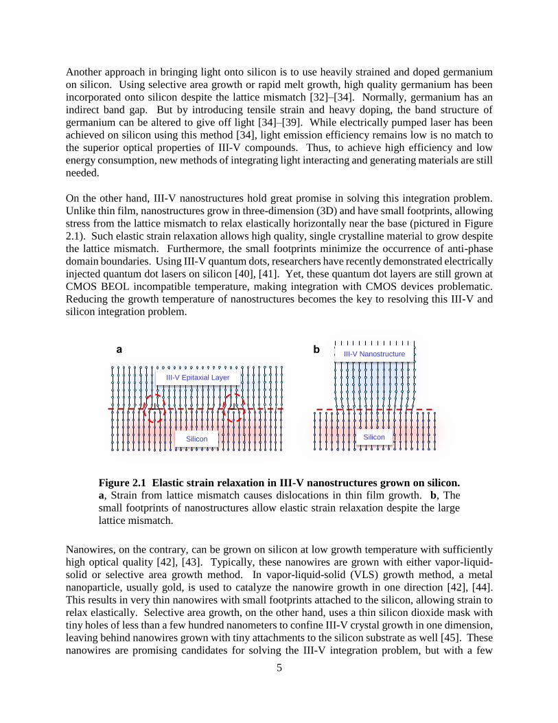
On the other hand, III-V nanostructures hold great promise in solving this integration problem.
Unlike thin film, nanostructures grow in three-dimension (3D) and have small footprints, allowing
stress from the lattice mismatch to relax elastically horizontally near the base (pictured in Figure
2.1). Such elastic strain relaxation allows high quality, single crystalline material to grow despite
the lattice mismatch. Furthermore, the small footprints minimize the occurrence of anti-phase
domain boundaries. Using III-V quantum dots, researchers have recently demonstrated electrically
injected quantum dot lasers on silicon [40], [41]. Yet, these quantum dot layers are still grown at
CMOS BEOL incompatible temperature, making integration with CMOS devices problematic.
Reducing the growth temperature of nanostructures becomes the key to resolving this III-V and
silicon integration problem.
Figure 2.1 Elastic strain relaxation in III-V nanostructures grown on silicon. a, Strain from lattice mismatch causes dislocations in thin film growth. b, The
small footprints of nanostructures allow elastic strain relaxation despite the large
lattice mismatch.
Nanowires, on the contrary, can be grown on silicon at low growth temperature with sufficiently
high optical quality [42], [43]. Typically, these nanowires are grown with either vapor-liquid-
solid or selective area growth method. In vapor-liquid-solid (VLS) growth method, a metal
nanoparticle, usually gold, is used to catalyze the nanowire growth in one direction [42], [44].
This results in very thin nanowires with small footprints attached to the silicon, allowing strain to
relax elastically. Selective area growth, on the other hand, uses a thin silicon dioxide mask with
tiny holes of less than a few hundred nanometers to confine III-V crystal growth in one dimension,
leaving behind nanowires grown with tiny attachments to the silicon substrate as well [45]. These
nanowires are promising candidates for solving the III-V integration problem, but with a few
┴ ┴
Silicon
III-V Epitaxial Layer
Silicon
III-V Nanostructure a b
6
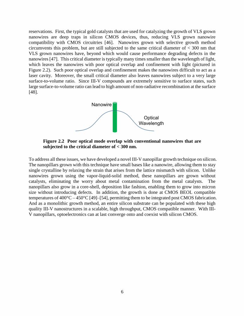
reservations. First, the typical gold catalysts that are used for catalyzing the growth of VLS grown
nanowires are deep traps in silicon CMOS devices, thus, reducing VLS grown nanowire
compatibility with CMOS circuitries [46]. Nanowires grown with selective growth method
circumvents this problem, but are still subjected to the same critical diameter of < 300 nm that
VLS grown nanowires have, beyond which would cause performance degrading defects in the
nanowires [47]. This critical diameter is typically many times smaller than the wavelength of light,
which leaves the nanowires with poor optical overlap and confinement with light (pictured in
Figure 2.2). Such poor optical overlap and confinement makes the nanowires difficult to act as a
laser cavity. Moreover, the small critical diameter also leaves nanowires subject to a very large
surface-to-volume ratio. Since III-V compounds are extremely sensitive to surface states, such
large surface-to-volume ratio can lead to high amount of non-radiative recombination at the surface
[48].
Figure 2.2 Poor optical mode overlap with conventional nanowires that are
subjected to the critical diameter of < 300 nm.
To address all these issues, we have developed a novel III-V nanopillar growth technique on silicon.
The nanopillars grown with this technique have small bases like a nanowire, allowing them to stay
single crystalline by relaxing the strain that arises from the lattice mismatch with silicon. Unlike
nanowires grown using the vapor-liquid-solid method, these nanopillars are grown without
catalysts, eliminating the worry about metal contamination from the metal catalysts. The
nanopillars also grow in a core-shell, deposition like fashion, enabling them to grow into micron
size without introducing defects. In addition, the growth is done at CMOS BEOL compatible
temperatures of 400°C – 450°C [49]–[54], permitting them to be integrated post CMOS fabrication.
And as a monolithic growth method, an entire silicon substrate can be populated with these high
quality III-V nanostructures in a scalable, high throughput, CMOS compatible manner. With III-
V nanopillars, optoelectronics can at last converge onto and coexist with silicon CMOS.
Nanowire
Optical Wavelength

7
2.1 Growth of (In)GaAs Nanopillars
Figure 2.3 As grown InGaAs nanopillars passivated with in situ GaAs shell.
To bridge the integration gap between III-V and silicon, we have developed a novel nanopillar
growth technique to integrate III-V onto silicon. This novel growth technique allows the growth
of single crystalline (In)GaAs [50] and InP nanopillars [51] onto silicon via metal-organic
chemical vapor deposition (MOCVD). Figure 2.3 shows some example scanning electron
micrographs (SEMs) of as-grown InGaAs nanopillars on silicon substrate. Although the growth
of (In)GaAs and InP nanopillars are very similar, we defer the discussion of InP nanopillar growth
until the next section. For (In)GaAs nanopillars, the growth took place on a deoxidized silicon
substrate that had been mechanically roughened just prior to growth. The growth then occurred
inside the MOCVD chamber at a relative low temperature of 400°C, well within the thermal budget
of contemporary CMOS [31]. Since the growth occurred at such a low temperature, precursor
gases tertiarybutylarsine (TBAs) and triethylgallium (TEGe) were used for their relatively low
decomposition temperatures of 380°C and 300°C, respectively. The mole fraction used are kept
constant during growth at 1.12 × 10⁻⁵ for TEGa and 5.42 × 10⁻⁴ for TBAs. Indium could also be
added to the growth chamber via trimethylindium (TMIn) to form InGaAs nanopillars. The mole
fractions of TMIn used for growing In0.12Ga0.88As is 9.86 × 10⁻⁷, and In0.2Ga0.8As is 1.73 × 10⁻⁶.
Figure 2.4 Growth of nanopillar. From nanocluster to layer-by-layer core-shell
growth to nanopillar. An in situ surface passivation layer can be added as well.
500 nm
Top View
Cluster Nucleation
Core-Shell Growth
Surface Passivation

8
Figure 2.5 Core-shell growth of nanopillar. The nanopillar starts as a
nanocluster, and grow bigger and bigger in a core-shell manner.
Once the precursor gases started flowing, nanoclusters would form spontaneously on the
roughened silicon substrate. These nanoclusters then grew bigger and bigger in a layer-by-layer
deposition like process along the [0001] crystal direction that results in a core-shell mode. This
core-shell growth process is better described schematically in Figure 2.4 and Figure 2.5. Because
of the core-shell growth, the anchorage point of the nanopillar is actually just the tiny nanocluster
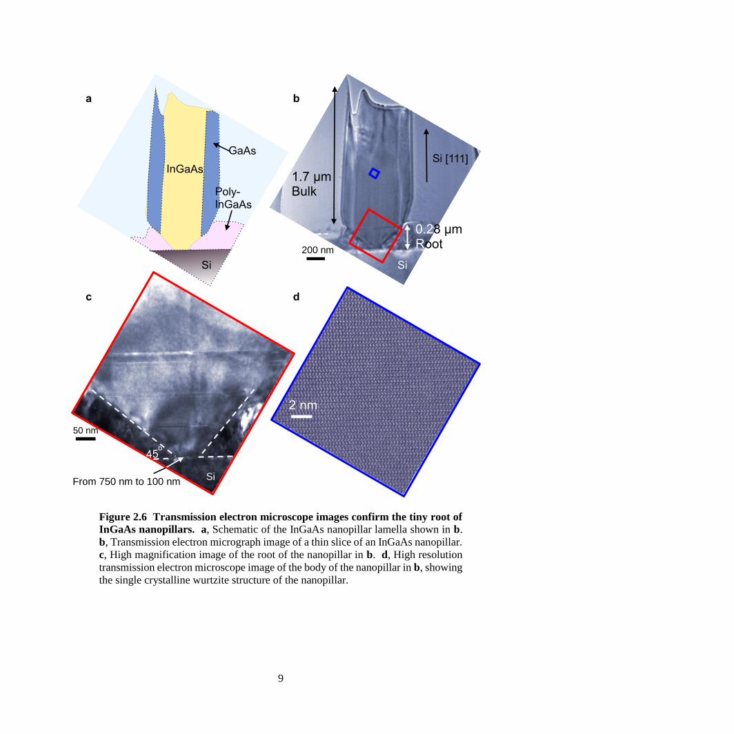
(see transmission electron microscope images in Figure 2.6) [52]. The tiny base allows the
nanopillar to grow well beyond the critical diameter of nanowire of < 300 nm [47] and into micron
size, as shown in Figure 2.3, by enlarging with this deposition like core-shell growth while
tolerating the 4% lattice mismatch from the substrate. The ability to grow into micron size
dimension dramatically reduces the effect of surface recombination by reducing the surface-to-
volume ratio. The core-shell growth also forces any dislocations that formed to extend horizontally,
leaving the body of the nanopillar remain single crystalline (Figure 2.6d). In fact, similarly grown
nanopillars have been shown to remain single crystalline even when grown on a sapphire substrate
with a whopping 46% lattice mismatch [55]. As we shall see later, the high crystal can be attested
to the bright photoluminescence emissions observed from these nanopillars. And since the
nanocluster origin favors wurtzite formation, the nanopillars remain in wurtzite form during the
subsequent metastable growth. This is unlike arsenide based thin film grown conventionally,
which typically take the zinc blende crystal phase [56]. Furthermore, the core-shell growth also
facilitates easy in-situ surface passivation via higher band gap cladding layers, as we can easily
switch precursor gases during growth to form an outer shell covering the entire nanopillar [57],
[58]. Typically when pure GaAs material is grown, the structure is shaped as an atomically sharp
needle [50]. Thus, we typically call these needle shaped GaAs nanostructures as “nanoneedles”.
But when indium is added and the nanoneedles are grown for longer than 60 minutes, indium
accumulation at the tips causes the structures to lose the needle shape and form flat tops, hence,
the name “nanopillar” for these truncated InGaAs nanocrystals [52]. InGaAs nanopillars with flat
tops are shown in the SEM images in Figure 2.7.
9
Figure 2.6 Transmission electron microscope images confirm the tiny root of
InGaAs nanopillars. a, Schematic of the InGaAs nanopillar lamella shown in b.
b, Transmission electron micrograph image of a thin slice of an InGaAs nanopillar.
c, High magnification image of the root of the nanopillar in b. d, High resolution
transmission electron microscope image of the body of the nanopillar in b, showing
the single crystalline wurtzite structure of the nanopillar.
Si
1.7 μm Bulk
0.28 μm Root
Si
200 nm
50 nm
Si From 750 nm to 100 nm
2 nm
a b
c d
10
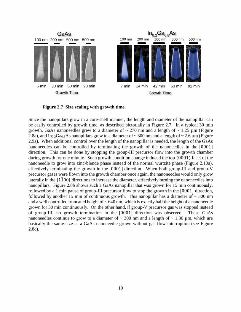
Figure 2.7 Size scaling with growth time.
Since the nanopillars grow in a core-shell manner, the length and diameter of the nanopillar can
be easily controlled by growth time, as described pictorially in Figure 2.7. In a typical 30 min
growth, GaAs nanoneedles grew to a diameter of ~ 270 nm and a length of ~ 1.25 µm (Figure
2.8a), and In0.2Ga0.8As nanopillars grew to a diameter of ~ 300 nm and a length of ~ 2.6 µm (Figure
2.9a). When additional control over the length of the nanopillar is needed, the length of the GaAs
nanoneedles can be controlled by terminating the growth of the nanoneedles in the [0001] direction. This can be done by stopping the group-III precursor flow into the growth chamber
during growth for one minute. Such growth condition change induced the top (0001) facet of the
nanoneedle to grow into zinc-blende phase instead of the normal wurtzite phase (Figure 2.10a),
effectively terminating the growth in the [0001] direction. When both group-III and group-V
precursor gases were flown into the growth chamber once again, the nanoneedles would only grow
laterally in the [1100] directions to increase the diameter, effectively turning the nanoneedles into
nanopillars. Figure 2.8b shows such a GaAs nanopillar that was grown for 15 min continuously,
followed by a 1 min pause of group-III precursor flow to stop the growth in the [0001] direction,
followed by another 15 min of continuous growth. This nanopillar has a diameter of ~ 300 nm
and a well controlled truncated height of ~ 640 nm, which is exactly half the height of a nanoneedle
grown for 30 min continuously. On the other hand, if group-V precursor gas was stopped instead
of group-III, no growth termination in the [0001] direction was observed. These GaAs
nanoneedles continue to grow to a diameter of ~ 300 nm and a length of ~ 1.36 µm, which are
basically the same size as a GaAs nanoneedle grown without gas flow interruption (see Figure
2.8c).
60 min 6 min 30 min 90 min
500 nm 500 nm 200 nm 100 nm
Growth Time
GaAs
Growth Time
500 nm 500 nm 500 nm 200 nm 100 nm
42 min 7 min 14 min 63 min 92 min
In0.2
Ga0.8
As

11
Figure 2.8 Controlling the size of GaAs nanoneedles. 30° tilt SEM images of
(a) a GaAs nanoneedle grown continuously for 30 min at 395°C, (b) half-length
GaAs nanopillars achieved by stopping group-III precursor flow for 1 min after a
15 min growth, followed by another 15 min growth, and (c) a GaAs nanoneedle
grown with a 1 min pause of group-V precursor after a 15 min growth, followed by
another 15 min growth. For all three cases, the diameters are the same at ~ 300 nm.
d, Average lengths and diameter growth rates for GaAs nanoneedles grown for 30
min under various growth conditions. The growth condition changes that stop the
[0001] growth happened 15 min into the growth.
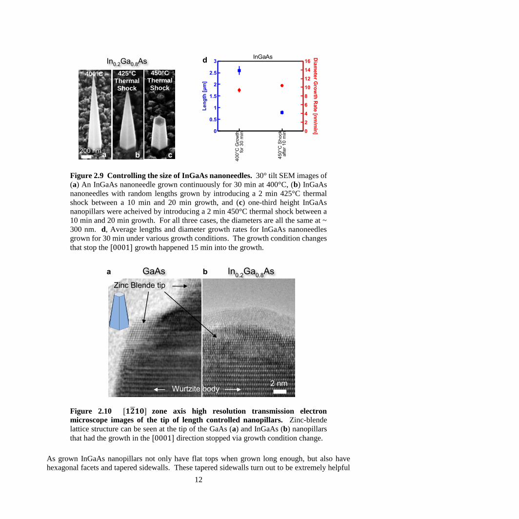
Similarly, the length of In0.2Ga0.8As nanoneedles can also be controlled by terminating the growth
in the [0001] direction with a similar change in growth condition. But instead of solely pausing
the group-III gas flow, the growth temperature was also raised rapidly from 400°C to 450°C under
only group-V gas flow for 2 min to stop the [0001] growth. Such growth condition change also
caused the top (0001) facet of the wurtzite InGaAs nanoneedle to grow into zinc-blende phase,
which then terminates the growth of the nanoneedle in the [0001] direction, such as shown in
Figure 2.10b. When the growth temperature was lowered back down to the typical growth
temperature of 400°C, the nanoneedles would only continue to grow laterally to form nanopillars.
Figure 2.9c shows an example of such nanopillar grown at 400°C for 10 min, followed by a 2 min
450°C thermal shock, followed by another 20 min of growth at 400°C. Nanopillars grown this
way have an average diameter of 310 nm and a height of 790 nm, which are about the same
diameter as nanoneedles grown continuously at 400°C, but at only about a third as tall. It is
interesting to note that if the thermal shock temperature was reduced from 450°C to 425°C, only
some of the nanoneedles showed truncated growth (see Figure 2.9b).
100 nm
GaAs
Continuous Stopping Group-III
Stopping Group-V
a b c
d
12
Figure 2.9 Controlling the size of InGaAs nanoneedles. 30° tilt SEM images of
(a) An InGaAs nanoneedle grown continuously for 30 min at 400°C, (b) InGaAs
nanoneedles with random lengths grown by introducing a 2 min 425°C thermal
shock between a 10 min and 20 min growth, and (c) one-third height InGaAs
nanopillars were acheived by introducing a 2 min 450°C thermal shock between a
10 min and 20 min growth. For all three cases, the diameters are all the same at ~
300 nm. d, Average lengths and diameter growth rates for InGaAs nanoneedles
grown for 30 min under various growth conditions. The growth condition changes
that stop the [0001] growth happened 15 min into the growth.
Figure 2.10 [𝟏��𝟏𝟎] zone axis high resolution transmission electron
microscope images of the tip of length controlled nanopillars. Zinc-blende
lattice structure can be seen at the tip of the GaAs (a) and InGaAs (b) nanopillars
that had the growth in the [0001] direction stopped via growth condition change.
As grown InGaAs nanopillars not only have flat tops when grown long enough, but also have
hexagonal facets and tapered sidewalls. These tapered sidewalls turn out to be extremely helpful
200 nm
In0.2Ga0.8As
400°C 425°C Thermal Shock
450°C Thermal Shock
a b c
d
2 nm Wurtzite body
Zinc Blende tip
In0.2
Ga0.8
As GaAs a b

13
in resonator design. Because of the tapered sidewalls, light trapped inside a nanopillar actually
bounces around in a helically propagating mode, allowing high quality factor (Q) resonance within
the nanopillar without detaching the pillar from the silicon substrate. Together with bright
photoluminescence, as grown InGaAs nanopillars can easily become lasers on silicon. Indeed,
under optical pumping, as grown nanopillars have been shown to lase while freestanding on the
silicon substrate [59]. Figure 2.11 below shows the narrow lasing spectra and characteristic S
shaped light input versus light output (L-L) dependence of a nanopillar laser under optical pumping
by a Ti:sapphire pulsed laser at low temperature of 4 K. Lasing under room temperature and
continuous wave operation have also been shown. Therefore, InGaAs nanopillars are the perfect
candidates in bringing laser light onto silicon substrates.
Figure 2.11 Nanopillar laser grown on silicon. a, Lasing spectra of as grown
nanopillar. b, Light input versus light output curve (L-L) of the lasing nanopillar
showing the characteristic S shaped dependence.
To show CMOS compatibility, we grew InGaAs nanopillar lasers on a chip with non-metalized
metal-oxide-semiconductor field effect transistors (MOSFETs) [54]. The nanopillars were grown
on places where silicon was exposed, such as the source, drain and gate of the MOSFETs. Figure
2.12 shows how the nanopillars are positioned on the MOSFETs. The resulting as-grown
nanopillars lased under optical pumping, as the L-L curve and narrow lasing spectrum in Figure
2.13 show. To establish CMOS compatibility, we compare the performance of the MOSFETs
before and after the nanopillar synthesis. Figure 2.14 displays the electrical characteristics of an
example MOSFET before and after growth. Here, both the transfer and output characteristics
remained largely unchanged. In fact, of the 60 MOSFETs tested, 59 MOSFETs characteristics
remained unchanged. Thus, this experiment establishes the CMOS compatibility of our nanopillar
synthesis process.
850 900 950 1000
0
100
200
300
Inte
ns
ity (
a.u
.)
Wavelength (nm)
1.8 Pth
1.0 Pth
0.8 Pth
0.3 Pth
0.1 Pth
Q~200 β~0.01
T=4K
Pth=22 µJ/cm2
Nth~1x10¹⁸
cm-3
1 10 100 1000 1E-6
1E-5
1E-4
1E-3
0.01
0.1
1
Pe
ak P
ow
er
(W)
Pump fluence (mJ/cm2)
a b
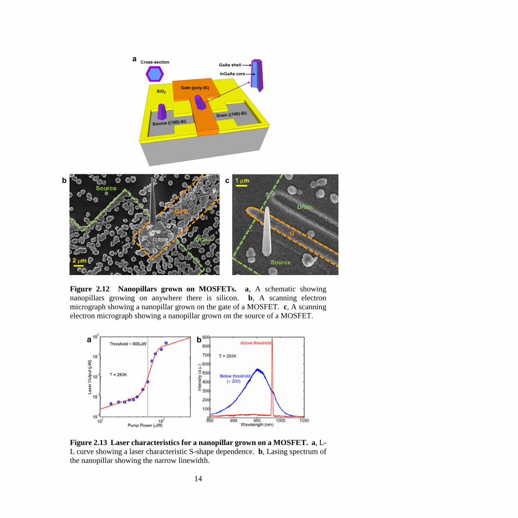
14
Figure 2.12 Nanopillars grown on MOSFETs. a, A schematic showing
nanopillars growing on anywhere there is silicon. b, A scanning electron
micrograph showing a nanopillar grown on the gate of a MOSFET. c, A scanning
electron micrograph showing a nanopillar grown on the source of a MOSFET.
Figure 2.13 Laser characteristics for a nanopillar grown on a MOSFET. a, L-
L curve showing a laser characteristic S-shape dependence. b, Lasing spectrum of
the nanopillar showing the narrow linewidth.
a
b c

15
Figure 2.14 MOSFET performance remains unchanged after nanopillar
growth. a, Transistor transfer characteristic before and after growth. b, Transistor
output characteristic also remains unchanged.
2.2 Growth of InP Nanopillars
High quality InP nanopillars can also be grown on silicon substrate in a similar manner. Using
MOCVD on deoxidized and mechanically roughened silicon substrates, single crystalline wurtzite
phase InP nanopillars were grown at CMOS BEOL compatible temperature of 450°C with
trimethylindium (TMIn) and tertiarybutylphosphine at mole fractions 4.73 × 10⁻⁶ and 5.9 × 10⁻⁴,
respectively [51]. These InP nanopillars also grew in a core-shell manner, allowing them to grow
into micron scale with growth time. Such time scaling features is displayed in Figure 2.15. As
shown in Figure 2.16, the core-shell growth also confines defects from lattice mismatch to the
roots, leaving the bodies of the nanopillars defect free.
Figure 2.15 Growth evolution of InP nanopillars (courtesy of Fan Ren of
reference [51]). Core-shell growth allows the size of InP nanopillars to scale with
growth time.
15 min
500 nm
22.5 min 30 min 37.5 min 45 min
Growth Time

16
Figure 2.16 Transmission electron microscope studies show the single
crystalline quality of InP nanopillars (from reference [51]). a, High resolution
transmission electron microscope image showing the wurtzite crystal structure of
an InP nanopillar. b, Diffraction pattern of a showing the perfect wurtzite crystal
diffraction pattern.
These InP nanopillars also show bright photoluminescence. In addition, InP material has one of
the best surface recombination characteristics among III-V compounds [60]. This makes InP
nanopillars very promising for achieving laser operation. Indeed, under pulse optical pumping
from a Ti:sapphire laser at 4 K, InP nanopillars lased while free-standing on silicon substrate [51].
The narrow lasing spectrum and light output versus light input (L-L) curve are shown in Figure
2.17. As a result, we now have two very promising material platforms that can possibly bring light
interaction to silicon CMOS.
Figure 2.17 Lasing from as grown InP nanopillars (from reference [51]). a,
Lasing spectrum of an InP nanopillar. b, S shaped light input versus light output
curve from the InP nanolaser in a.
a b
a b

17
Chapter 3
Site Control Growth of Nanopillars
The nanopillar growth presented in Chapter 2 provides a promising pathway towards integrating
high quality, optically active III-V materials onto silicon substrate, which opens up new
opportunities in converging photonics and electronics towards a common platform. While
remarkable, nanopillars grown with previously discussed techniques nucleate at random locations.
In many practical applications, however, precise control over the growth locations of the
nanopillars is crucial to interfacing devices built with nanopillars to the rest of the circuit. This
has led to many research groups to develop techniques, such as selective area growth [45], [61]–
[67] and metal catalyst patterning [68]–[71], to precisely control the growth locations of nanowires.
Since our nanopillars grow without catalysts, we adopt the former nucleation control technique.
In this Chapter, we discuss our research progress into developing site controlled growth of III-V
nanopillars.
3.1 Site Controlled Growth of InGaAs Nanopillars
Figure 3.1 Processing steps to prepare for selective area growth. a, Thermal
oxidation to create growth control mask on silicon substrate. b, Deep ultra-violet
lithography is used to create hole patterns on the growth mask. c, Nanopillar
growth takes place only at the mask openings.
The nucleation locations of nanopillars can be controlled by masking away regions on the silicon
substrate where growth is unwanted, hence, the name selective area growth. To do this, we used
silicon dioxide as a mask, and leave behind holes where we wanted nanopillars to growth. The
mask we used is 20 nm of thermally grown silicon dioxide. This silicon dioxide layer was
Silicon Silicon Silicon
a b c
Thermal Oxidation Lithography and Etching Selective Area Growth
SiO2 SiO2 SiO2

18
patterned with deep ultra-violet (DUV) lithography to generate holes that were 260 – 400 nm in
diameter, and spaced 0.8 – 10 µm apart. Unlike other approaches that require electron beam
lithography, our use of DUV lithography allows low cost, high throughput patterning throughout
the entire wafer. After lithography, we used buffered hydrofluoric (BHF) to etch the lithography
pattern into the silicon dioxide mask. The photoresist was subsequently removed in PRS-3000,
followed by a quick oxygen plasma de-scum. Before the substrate was loaded into the MOCVD,
the substrate was submerged in diluted (100:1) BHF one more time to get rid of any contaminants
on the oxide surface, and to ensure that the patterned holes were oxide free. This final de-oxidation
step reduced the oxide thickness to ~ 14 nm. Figure 3.1 below summarizes the fabrication steps.
Figure 3.2 shows an atomic force microscope image of the fabricated silicon dioxide growth mask.
Figure 3.2 Atomic force microscope image of fabricated silicon dioxide site
control mask. The holes here are 400 nm in diameter and spaced 800 nm apart.
The image is scaled so that the holes are at a height of 0 nm.
During growth, the nanopillars initiated by spontaneous clustering within the patterned holes and
subsequently formed by a deposition-like process that results in a core-shell growth mode. The
core-shell growth mode allows easy cladding of the nanopillars with a GaAs shell for surface
passivation. Unlike typical InGaAs material, the nanopillars are in pure Wurtzite phase, growing
along the [0001] direction. The size of the pillars can be scaled easily by growth time and indium
composition [52]. Figure 3.3 below shows the preliminary result of the patterned growth. The
percentage of holes filled is modest at 19% for an array of holes that are 400 nm wide and 6 µm
apart. The low yield can be attributed to the presence of the silicon dioxide mask altering the
nucleation and growth condition. In fact, it has been shown that the silicon dioxide mask used in
selective area growth significantly enhances the diffusion lengths of the indium and gallium
adatoms [45], [72]. The enhanced diffusion lengths likely allow too much indium and gallium
adatoms to accumulate within the openings, disrupting the harmonious balance between group III
and group V adatoms that is crucial to the nucleation and growth of the nanopillars [52]. We hope
to improve the yield with further optimization in growth conditions and mask preparation.
500 nm

19
Figure 3.3 Site controlled growth of In0.2Ga0.8As nanopillars. a, Scanning
electron microscope image showing the regular array of nanopillars. b, Zoomed
in scanning electron microscope image taken at 30° angle. c, Scanning electron
microscope image taken from the top.
For example, one optimization that can be done to improve the yield is to reduce the indium flow
to compensate for the extra indium adatoms diffused from the silicon dioxide mask. By reducing
the indium precursor flow from 7 sccm to 4 sccm while keeping everything else the same,
nucleation took place in almost every single hole (see Figure 3.4). Although this is a marked
improvement over the previous result, however, nucleated nanoclusters failed to continue to grow
in the vertical direction to form the usual micron long nanopillars. As Figure 3.4 shows, even after
15 minute of growth, the nucleated seeds grew to a height of around 300 nm, as opposed to the
expected 2 µm height. This truncated growth is likely a result of an imbalance between the gallium
and indium precursors during growth, which can disrupt nanopillar growth in the vertical direction
as previously discussed in Section 2.1 and Reference [52].
Another optimization that can be done to improve yield is to use smaller patterned holes to avoid
having multiple nanopillars per hole. As depicted in Figure 3.4, nucleation happens along the edge
of the hole opening. When the hole is too big, more than one nucleation event can happen within
the same hole. Since the DUV tool available to us has a resolution limit of 250 nm, we turned to
electron beam lithography to pattern smaller holes. Figure 3.5 shows the result of site controlled
growth with the smaller holes. When the holes are smaller than 60 nm, no nanopillar nucleation
took place. Nanopillars only nucleated when the holes are about 80 nm big. But when the holes
are bigger than 90 nm, multiple nanopillars started to emerge from the same hole. Therefore, for
InGaAs nanopillars, the optimal hole dimension to get one nanopillar per hole is around 80 nm.
10 μm
2 μm
30 tilt SEM
Top view SEM
1 μm
a
b
c
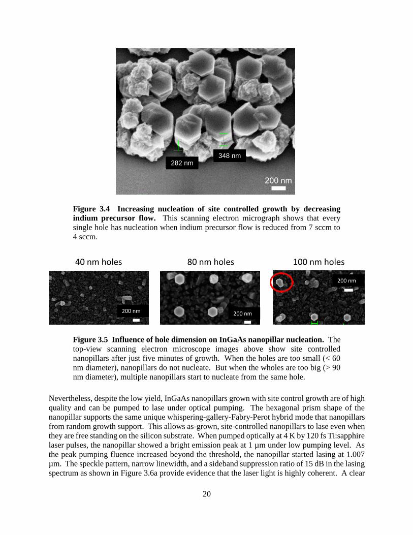
20
Figure 3.4 Increasing nucleation of site controlled growth by decreasing
indium precursor flow. This scanning electron micrograph shows that every
single hole has nucleation when indium precursor flow is reduced from 7 sccm to
4 sccm.
Figure 3.5 Influence of hole dimension on InGaAs nanopillar nucleation. The
top-view scanning electron microscope images above show site controlled
nanopillars after just five minutes of growth. When the holes are too small (< 60
nm diameter), nanopillars do not nucleate. But when the wholes are too big (> 90
nm diameter), multiple nanopillars start to nucleate from the same hole.
Nevertheless, despite the low yield, InGaAs nanopillars grown with site control growth are of high
quality and can be pumped to lase under optical pumping. The hexagonal prism shape of the
nanopillar supports the same unique whispering-gallery-Fabry-Perot hybrid mode that nanopillars
from random growth support. This allows as-grown, site-controlled nanopillars to lase even when
they are free standing on the silicon substrate. When pumped optically at 4 K by 120 fs Ti:sapphire
laser pulses, the nanopillar showed a bright emission peak at 1 µm under low pumping level. As
the peak pumping fluence increased beyond the threshold, the nanopillar started lasing at 1.007
µm. The speckle pattern, narrow linewidth, and a sideband suppression ratio of 15 dB in the lasing
spectrum as shown in Figure 3.6a provide evidence that the laser light is highly coherent. A clear
200 nm
282 nm 348 nm
200 nm
200 nm
200 nm
80 nm holes 40 nm holes 100 nm holes

21
threshold of 40 µJ/cm2 pumping fluence can also be seen on the light output as a function of pump
fluence curve (L-L curve) as shown in Figure 3.6b. Since the nanopillar dimension is scalable
with growth time, resonance can be tuned easily by changing growth time. The emission
wavelength can also be adjusted to match the resonance peak by incorporating more indium into
the nanopillar during growth. With further optimization, it is possible to create site-controlled
nanolasers that emit at silicon transparent wavelengths. For the nanopillar lasers used in this study,
they are typically 4 µm tall and 700 nm wide in base diameter after 28 minutes of growth.
Figure 3.6 Lasing characteristics of site controlled InGaAs nanopillar. a,
Lasing emission from a site controlled InGaAs nanopillar. The inset shows the
microscope image of the speckle pattern observed when the nanopillar is lasing. b,
A clear threshold of 40 µJ/cm2 pumping fluence can be seen on the light output as
a function of pump fluence curve (L-L curve).
3.2 Site Controlled Growth of InP Nanopillars
Similarly, the location of InP nanopillars can also be controlled by using a silicon dioxide mask to
confine growth to predefined locations. The process of preparing this silicon dioxide mask is very
similar to the one used for InGaAs nanopillars, but with a few notable exceptions. For InP
nanopillars, instead of using a thermally grown silicon dioxide layer as the growth mask, we used
a 135 nm thick silicon dioxide that was deposited with plasma enhanced chemical vapor deposition
(PECVD). The reason for this change is that the growth mask for InP nanopillars needs to be
roughened mechanically before growth, and silicon dioxide deposited by PECVD allows this to
happen much more easily than the high quality, smooth silicon dioxide grown by oxidation. The
silicon dioxide mask was then patterned with the same DUV mask that was used in the InGaAs
nanopillar experiment, with hole diameters ranging from 260 – 400 nm, and spacings of 0.8 – 10
µm. The hole openings were transferred onto the silicon dioxide with plasma etching in CF4. After
removal of the photoresist, the silicon substrate was etched and roughened in heated
tetramethylammonium hydroxide. The surface of the silicon dioxide mask was also mechanically
roughened before growth. We found that these roughening steps significantly improve nucleation.

22
A final de-oxidation step in 10:1 BHF was added just before growth. This reduced the thickness
of the patterned mask to about 100 nm.
Figure 3.7 Site controlled growth of InP nanopillars. a, Scanning electron
micrograph image of InP nanopillars in a regular array. The holes are 380 nm wide
and spaced 10 µm apart. b, Close-up view of InP nanopillars grown in an array of
holes that are 380 nm wide and spaced 6 µm apart.
The patterned substrate was grown in the MOCVD using standard InP nanopillar growth recipe.
Figure 3.7 shows the results from the site controlled growth. Regular arrays of InP nanopillars
with 10 and 6 µm spacings can be easily seen. Here, we found that the number of upright
nanopillars over the number of patterned holes, or simply called yield, is as high as 66% for holes
that are 400 nm wide and spaced 10 µm apart. This is a remarkable improvement over the 19%
yield that we got with InGaAs nanopillars. We attribute the much higher success rate of InP to the
relatively simpler binary composition, which cuts down on the complexity and optimization
needed to balance the flow of the precursor gases.
We also found that the hole diameter and spacing influence the percentage of holes filled with
nanopillars considerably. Figure 3.8 shows the influence of hole diameter on nucleation
percentage. When the hole diameter is less than 300 nm, we found the filling ratio to be rather
poor. This is likely due to smaller holes being ineffective at capturing the precursor adatoms, thus,
reducing the probability of nanopillar nucleation. But when the hole diameter is too large, multiple
nanopillars start to nucleate from within the same hole. Thus, an optimal hole diameter is found
to be somewhere between 340 – 400 nm. There is also an optimal range of spacing between holes.
The yield is found to drop significantly when the holes are too closely packed, especially for holes
spaced below 1 µm. Although the 1 µm spacing SEM image shown in Figure 3.9 looks to be very
densely populated, however, the yield is merely 20%, far lower than the 66% yield with 10 µm
spacing. We believe the closely packed condition creates competition and scarcity of precursor
adatoms among the nanopillars, which ultimately leads to poor nucleation. Though, we believe
the yield can be further improved through mask design and growth condition optimization.
10 µm
a
2 µm
b

23
Figure 3.8 Influence of hole diameter on site controlled growth of InP
nanopillars. When the holes are too small, the percentage of holes filled drops.
260 nm hole, 1 µm spacing 280 nm hole, 1 µm spacing
10 µm 10 µm
300 nm hole, 1 µm spacing
10 µm
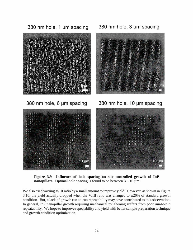
24
Figure 3.9 Influence of hole spacing on site controlled growth of InP
nanopillars. Optimal hole spacing is found to be between 3 – 10 µm.
We also tried varying V/III ratio by a small amount to improve yield. However, as shown in Figure
3.10, the yield actually dropped when the V/III ratio was changed to ±20% of standard growth
condition. But, a lack of growth run-to-run repeatability may have contributed to this observation.
In general, InP nanopillar growth requiring mechanical roughening suffers from poor run-to-run
repeatability. We hope to improve repeatability and yield with better sample preparation technique
and growth condition optimization.
380 nm hole, 1 µm spacing
10 µm
380 nm hole, 3 µm spacing
10 µm
380 nm hole, 6 µm spacing
10 µm
380 nm hole, 10 µm spacing
10 µm

25
Figure 3.10 Varying V/III ratio to improve yield of InP nanopillar site
controlled growth. But yield is found to be quite near optimum at standard growth
condition. At -20% and +20% of standard V/III ratio for InP nanopillar growth,
yield for site controlled growth drops significantly.
Nevertheless, the quality of InP nanopillars grown with site controlled growth are excellent. To
examine the quality of InP nanopillars grown by site controlled growth, we used focus ion beam
to cut open a cross section of the nanopillar and examined it under a transmission electron
microscope (TEM). This cross section was made through the center of the silicon dioxide opening,
and ran along the length of the nanopillar. Figure 3.11 shows the results of the TEM investigation.
As shown in Figure 3.11, the InP nanopillar grown with site control growth has high material
quality. There are only a few stack faults running horizontally across the nanopillar, and these
stacking faults are largely confined to the base of the nanopillar. The nanopillar also makes direct
contact to the silicon substrate, which makes device electrical contact through the substrate
possible. And more importantly, the nanopillar actually completely filled and overgrew the silicon
dioxide mask opening. Since the nanopillars grow in a core-shell manner, we can use this
overgrowth method to grow p-n junctions that are naturally electrically insulated from the silicon
substrate. Take Figure 3.12 as an example. If we grow a p-doped nanopillar to a size bigger than
the mask opening and overgrow the opening with an n-doped shell, the n-doped shell will be
electrically insulated from the substrate by the silicon dioxide mask. This makes device fabrication
as simple as simply putting on a pair of top and bottom contacts. Together with the ability to
precisely control the location of nanopillars, site controlled growth makes electronic-photonic
integration with nanopillars one step closer.
2 µm 2 µm
-20% V/III Ratio +20% V/III Ratio

26
Figure 3.11 Transmission electron microscope images of an InP nanopillar
grown with site controlled growth. The images show that the nanopillar base
completely fills the hole used for site control, and it makes direct contact to the
silicon substrate. The nanopillar also has excellent material quality with only a few
stacking faults running horizontally, but largely confined to the base of the
nanopillar.
Cross-sectional TEM
SiO2 mask
Si substrate
Mask opening
50 nm
5 nm
Si substrate
InP
InP
InP
Si substrate
Mask opening

27
Figure 3.12 Site controlled growth provides natural electrical isolation for p-
n junctions. Here, the n-doped shell is electrically isolated from the silicon
substrate because of the overgrowth and silicon dioxide mask used for site
controlled growth.
Si (111)
Mask opening
p
n

28
Chapter 4
Resonant Nanopillar Light Emitting Diode
Light source is an essential component to almost any photonic systems. And in many applications,
electrically driven laser is a necessary component. In Chapter 2, we show that nanopillars grown
on silicon lase under optical pumping owing to its natural support of strong resonance. In this
chapter, we show that by embedding the nanopillars within a metal-optic cavity that doubles as
metal contact, nanopillars can be fabricated into light emitting diodes (LEDs) that produce
stimulated emission under electrical control. Although the devices failed to reach condition
necessary for lasing, however, achieving stimulated emission from a nanoscale device on silicon
is a remarkable achievement that also serves as a great milestone and monumental leap towards
realizing nanolaser on silicon. And for some applications that do not require strictly coherent light
source, such an LED may suffice. With further optimization on design and processing, electrically
driven lasing from nanopillar on silicon may become possible.
4.1 Introduction to Electrically Driven Nano Light
Emitters
Integrating light emitters on-chip alongside electronics can enable many exciting new applications.
In some applications requiring dense array of light emitters, such as the case in on-chip optical
interconnects, sub-wavelength nano light emitters are highly desirable since conventional light
emitters are gargantuan compared to transistors. With nano light emitters, the tiny footprints allow
tight integration with electronics without sacrificing much on die area that could have used for
memory or logic operations. In addition, nano light emitters have less volume to pump, making
low energy operation possible.
Recently, there has been intense research interest in electrically driven nanolasers. This includes
demonstration of electrically driven nanolasers using wiped down cadmium sulphide nanowires
[73], free-standing III-V nanowires and nanopillars enclosed in metal cavities [74]–[78], nanosize
III-V waveguides embedded in metal cavities [75], and metal cavity surface emitting microlasers
[79], [80]. In almost all of these demonstrations, a metal-optic cavity is used to confine light into
a piece of semiconductor smaller than the wavelength of light. Though, introducing metal cavity
to nanolaser is of no easy task since metal is very lossy optically. Nevertheless, through careful
optical cavity design and high gain semiconductor materials, the loss of the metal cavity can be
overcome and, thus, lasing can be achieved. With this, pulsed [75], [79], [80], and even continuous
wave lasing [74], [77], [78] have been attained. And recently, with further optimization, room
temperature electrically driven lasing is also achieved with these metal cavity nanolasers [75], [77].

29
Although room temperature, electrically controlled continuous wave lasing operation has been
accomplished with nanolasers, these demonstrations are either done on the III-V semiconductor
native substrates, or through transfer methods to get the lasers onto silicon substrates. Therefore,
these demonstrations still suffer from the difficulties in integrating with electronics as described
in Chapter 2. Here, we propose to build nanolasers on silicon using nanopillars by exploiting the
natural resonance and high optical gain of nanopillars.
4.2 Fabricating Nanopillar into Electrical Device
In Chapter 2, we discuss the awesome optical properties of nanopillars. Here we show how we
can turn these nanopillars into electrical devices with excellent optical properties. For this section,
we limit our discussion on fabrication steps to InGaAs based nanopillars. We discuss fabrication
steps for InP based nanopillar in the next chapter. But before we can discuss the fabrication process,
we need to discuss growth briefly to explain how we dope the nanopillars to create useful electrical
junctions. A nice consequence of the core-shell growth mode as discussed in Chapter 2 is that the
nanopillar can be doped in situ during growth by flowing zinc (p-type) or tellurium (n-type)
dopants into the growth chamber to create p-i-n junctions in the radial direction of the nanopillars.
Such radial p-i-n junction is schematically shown in Figure 4.1c and Figure 4.3a. A scanning
electron microscope (SEM) image of an as-grown nanopillar featuring such p-i-n junction is shown
in Figure 4.1a. Typical indium composition used in our InGaAs nanopillars is around 20%, which
yields luminescence at around 980 nm.
Figure 4.1 InGaAs Nanopillar and LED devices. a, 60° tilt SEM image of as-
grown nanopillar with radial p-i-n layers. b, 45° tilt SEM image of a fabricated
LED device. c, Schematic illustrating a nanopillar device embedded inside a metal
cavity as a step toward electrically driven diode laser on silicon.
After growth, gold or silver metal contact, which also serves as a metal-optic cavity, was fabricated
over individual nanopillars without detaching them from the silicon substrate. Figure 4.3 below
summarizes the fabrication process flow as a flow chart. The processing steps are quite involved
actually for two main reasons: 1) lack of site controlled growth yield, and 2) parasitic growth of a
polycrystalline layer that shorts the p-doped shell to the substrate (depicted in Figure 2.5 and Figure
a b c
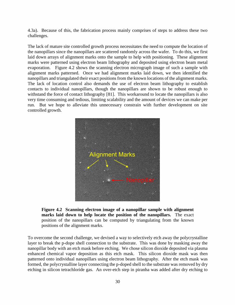
30
4.3a). Because of this, the fabrication process mainly comprises of steps to address these two
challenges.
The lack of mature site controlled growth process necessitates the need to compute the location of
the nanopillars since the nanopillars are scattered randomly across the wafer. To do this, we first
laid down arrays of alignment marks onto the sample to help with positioning. These alignment
marks were patterned using electron beam lithography and deposited using electron beam metal
evaporation. Figure 4.2 shows the scanning electron micrograph image of such a sample with
alignment marks patterned. Once we had alignment marks laid down, we then identified the
nanopillars and triangulated their exact positions from the known locations of the alignment marks.
The lack of location control also demands the use of electron beam lithography to establish
contacts to individual nanopillars, though the nanopillars are shown to be robust enough to
withstand the force of contact lithography [81]. This workaround to locate the nanopillars is also
very time consuming and tedious, limiting scalability and the amount of devices we can make per
run. But we hope to alleviate this unnecessary constrain with further development on site
controlled growth.
Figure 4.2 Scanning electron image of a nanopillar sample with alignment
marks laid down to help locate the position of the nanopillars. The exact
position of the nanopillars can be computed by triangulating from the known
positions of the alignment marks.
To overcome the second challenge, we devised a way to selectively etch away the polycrystalline
layer to break the p-dope shell connection to the substrate. This was done by masking away the
nanopillar body with an etch mask before etching. We chose silicon dioxide deposited via plasma
enhanced chemical vapor deposition as this etch mask. This silicon dioxide mask was then
patterned onto individual nanopillars using electron beam lithography. After the etch mask was
formed, the polycrystalline layer connecting the p-doped shell to the substrate was removed by dry
etching in silicon tetrachloride gas. An over-etch step in piranha was added after dry etching to
Nanopillar
Alignment Marks

31
ensure that the connection from the p-doped shell to the substrate was completely removed. The
resulting structure is schematized in Figure 4.3g.
After solving the two main hurdles, the nanopillars were electrically isolated with 200 nm of silicon
dioxide. This silicon dioxide layer also serves as a spacer separating the optical mode from the
lossy metal contacts. Therefore, the thickness of this silicon dioxide layer directly affects the
quality factor and confinement factor of the metal cavity.
Before contact metal was deposited, the silicon dioxide on the top portion of the nanopillar was
removed for electrical contact (Figure 4.3h). This was done with a photoresist etch-back process
to expose the nanopillar tips. This involved spinning photoresist onto the sample, and then etching
away the photoresist on the nanopillar tips with oxygen plasma. The result after this step is
schematized in Figure 4.3i. Now with photoresist protecting the bottom part of the nanopillars,
we etched away the silicon dioxide on the nanopillar tips with a simple wet etch in hydrofluoric
acid.
At this stage, the nanopillars were ready for metal contacts. Here we used electron beam
lithography and evaporation to put metal contacts to single nanopillars. Since this metal contact
doubles as a metal-optic cavity, the smoothness, quality and thickness of this metal contact are
rather important as these parameters directly affect the quality factor of the cavity. Also, to ensure
that the optical mode can be well confined within the nanopillar, a rather thick, 400 nm of metal
was used as contact. We initially used gold as the contact metal since it does not oxidize and it
makes good contact to GaAs based materials. But we later moved onto using silver as the contact
metal hoping to reduce the metal optical loss. Indeed, our experimental data showed much better
cavity performance from the silver encapsulated devices. Figure 4.1b shows a SEM image of a
fabricated device, along with the stylized schematics in Figure 4.1c.

32
Figure 4.3 Process flow of nanopillar device. a, Nanopillar structure after growth.
The red arrow denotes the current leakage path to be eliminated during fabrication.
b, Alignment marks are laid down just after growth using electron beam lithography
to help locate the nanopillars. c, Alignment marks metal evaporation and nanopillar
location registration. d, Silicon dioxide, which is later used as an etch mask, is
deposited everywhere via plasma enhanced chemical vapor deposition. e, Electron
Polycrystalline layer
n+ Si(111)
n+ Si(111)
p-contact
n-contact
n+ Si(111)
Nanopillar Growth
n+ Si(111)
n+ Si(111) n+ Si(111)
n+ Si(111)
n+ Si(111)
n+ Si(111)
SiO2 Etch Mask Deposition Etch Mask Definition SiO
2 Etch Mask Etch
Dry + Wet Etch of Poly-Layer SiO2 Electrical Isolation Photoresist Etch Back
Expose Tip for Contact Metal Contact Deposition
a b c
g h i
j k l
n+ Si(111)
Alignment Mark Lithography p-GaAs – 42 nm i-GaAs – 42 nm i-In
0.20Ga
0.80As – 170 nm
n-In0.12
Ga0.88
As – 400 nm i-In
0.12Ga
0.88As – 70 nm
n+ Si(111)
Alignment Mark Evaporation
d e f
n+ Si(111)
Contact Pad Lithography
Leakage path
Photoresist
Photoresist
SiO2
Photoresist
Alignment mark
Photoresist
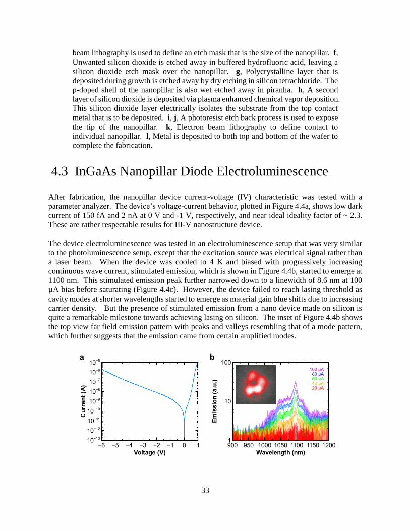
33
beam lithography is used to define an etch mask that is the size of the nanopillar. f,
Unwanted silicon dioxide is etched away in buffered hydrofluoric acid, leaving a
silicon dioxide etch mask over the nanopillar. g, Polycrystalline layer that is
deposited during growth is etched away by dry etching in silicon tetrachloride. The
p-doped shell of the nanopillar is also wet etched away in piranha. h, A second
layer of silicon dioxide is deposited via plasma enhanced chemical vapor deposition.
This silicon dioxide layer electrically isolates the substrate from the top contact
metal that is to be deposited. i, j, A photoresist etch back process is used to expose
the tip of the nanopillar. k, Electron beam lithography to define contact to
individual nanopillar. l, Metal is deposited to both top and bottom of the wafer to
complete the fabrication.
4.3 InGaAs Nanopillar Diode Electroluminescence
After fabrication, the nanopillar device current-voltage (IV) characteristic was tested with a
parameter analyzer. The device’s voltage-current behavior, plotted in Figure 4.4a, shows low dark
current of 150 fA and 2 nA at 0 V and -1 V, respectively, and near ideal ideality factor of ~ 2.3.
These are rather respectable results for III-V nanostructure device.
The device electroluminescence was tested in an electroluminescence setup that was very similar
to the photoluminescence setup, except that the excitation source was electrical signal rather than
a laser beam. When the device was cooled to 4 K and biased with progressively increasing
continuous wave current, stimulated emission, which is shown in Figure 4.4b, started to emerge at
1100 nm. This stimulated emission peak further narrowed down to a linewidth of 8.6 nm at 100
µA bias before saturating (Figure 4.4c). However, the device failed to reach lasing threshold as
cavity modes at shorter wavelengths started to emerge as material gain blue shifts due to increasing
carrier density. But the presence of stimulated emission from a nano device made on silicon is
quite a remarkable milestone towards achieving lasing on silicon. The inset of Figure 4.4b shows
the top view far field emission pattern with peaks and valleys resembling that of a mode pattern,
which further suggests that the emission came from certain amplified modes.
a b
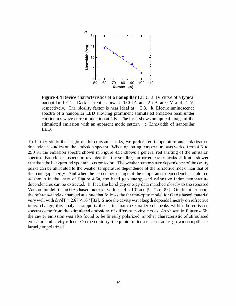
34
Figure 4.4 Device characteristics of a nanopillar LED. a, IV curve of a typical
nanopillar LED. Dark current is low at 150 fA and 2 nA at 0 V and -1 V,
respectively. The ideality factor is near ideal at ~ 2.3. b, Electroluminescence
spectra of a nanopillar LED showing prominent stimulated emission peak under
continuous wave current injection at 4 K. The inset shows an optical image of the
stimulated emission with an apparent mode pattern. c, Linewidth of nanopillar
LED.
To further study the origin of the emission peaks, we performed temperature and polarization
dependence studies on the emission spectra. When operating temperature was varied from 4 K to
250 K, the emission spectra shown in Figure 4.5a shows a general red shifting of the emission
spectra. But closer inspection revealed that the smaller, purported cavity peaks shift at a slower
rate than the background spontaneous emission. The weaker temperature dependence of the cavity
peaks can be attributed to the weaker temperature dependence of the refractive index than that of
the band gap energy. And when the percentage change of the temperature dependencies is plotted
as shown in the inset of Figure 4.5a, the band gap energy and refractive index temperature
dependencies can be extracted. In fact, the band gap energy data matched closely to the reported
Varshni model for InGaAs based material with α = 4 × 10⁴ and β = 226 [82]. On the other hand,
the refractive index changed at a rate that follows the thermo-optic model for GaAs based material
very well with dn/dT = 2.67 × 10⁻⁴ [83]. Since the cavity wavelength depends linearly on refractive
index change, this analysis supports the claim that the smaller sub peaks within the emission
spectra came from the stimulated emissions of different cavity modes. As shown in Figure 4.5b,
the cavity emission was also found to be linearly polarized, another characteristic of stimulated
emission and cavity effect. On the contrary, the photoluminescence of an as-grown nanopillar is
largely unpolarized.
c

35
Figure 4.5 Temperature and polarization dependence data of a LED device. a, The temperature dependence spectra show red shifting of the emission
wavelengths as temperature is increased. When the smaller sub peaks (highlighted
by colored arrows) and the overall spontaneous emissions are fitted and plotted
against temperature as shown in the inset, the sub peaks are revealed to shift at a
slower rate than the spontaneous emission peaks. In fact, the sub peaks shift at a
rate expected for the refractive index, while the spontaneous emission peaks shift
according to the Varshni model for band gap energies. For this experiment, 20 ns
current pulses were used to minimize heating effects. b, Although the
photoluminescence of an as-grown nanopillar (black) shows no polarization
dependence, the LED emission at 1.1 µm in Figure 4.4b shows large polarization
dependence (red). The grey hexagon in the center depicts the crystal orientation of
the nanopillar.
4.4 High Speed Operation of Nanopillar LED
For the LED to be useful for on-chip communication, the LED needs to be capable of operating at
high speed. Certainly, the impulse response in Figure 4.6a shows that such nano LED can indeed
be modulated at high speed. When a 0.8 ns pulse was sent to the LED, the LED responded quickly
with a rise time of 140 ps and a decay time of 300 ps. This suggests that the LED can potentially
be modulated at > 1 GHz. In fact, when a 2.5 GHz signal was directly sent to the LED, the LED
switched on and off quickly enough to show a clear modulated signal at 2.5 GHz (shown in Figure
4.6b). We believe that the small size of the nanopillar lends itself very well for high speed
operation because of the small capacitance. However, thus far, our device structure design
neglected the parasitic effects of the metal contacts. With further optimization, we expect the LED
to have even greater bandwidth.
4 K 20 K
40 K
80 K
120 K
150 K
200 K 250 K
0 50 100 150 200
0
1
2
3
Pe
rce
nt sh
ift
Temperature (K)
a
0O
30O
60O
90O
120O
150O
180O
210O
240O
270O
300O
330O
b
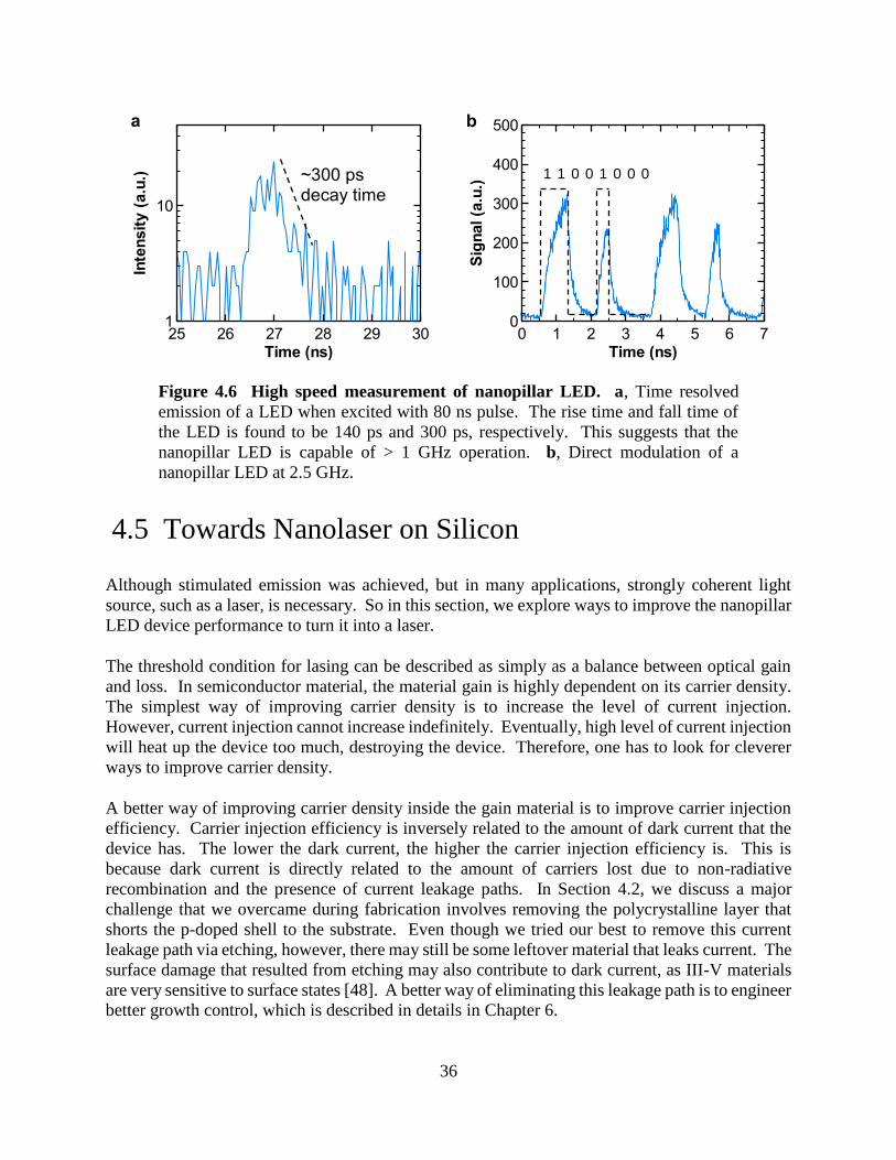
36
Figure 4.6 High speed measurement of nanopillar LED. a, Time resolved
emission of a LED when excited with 80 ns pulse. The rise time and fall time of
the LED is found to be 140 ps and 300 ps, respectively. This suggests that the
nanopillar LED is capable of > 1 GHz operation. b, Direct modulation of a
nanopillar LED at 2.5 GHz.
4.5 Towards Nanolaser on Silicon
Although stimulated emission was achieved, but in many applications, strongly coherent light
source, such as a laser, is necessary. So in this section, we explore ways to improve the nanopillar
LED device performance to turn it into a laser.
The threshold condition for lasing can be described as simply as a balance between optical gain
and loss. In semiconductor material, the material gain is highly dependent on its carrier density.
The simplest way of improving carrier density is to increase the level of current injection.
However, current injection cannot increase indefinitely. Eventually, high level of current injection
will heat up the device too much, destroying the device. Therefore, one has to look for cleverer
ways to improve carrier density.
A better way of improving carrier density inside the gain material is to improve carrier injection
efficiency. Carrier injection efficiency is inversely related to the amount of dark current that the
device has. The lower the dark current, the higher the carrier injection efficiency is. This is
because dark current is directly related to the amount of carriers lost due to non-radiative
recombination and the presence of current leakage paths. In Section 4.2, we discuss a major
challenge that we overcame during fabrication involves removing the polycrystalline layer that
shorts the p-doped shell to the substrate. Even though we tried our best to remove this current
leakage path via etching, however, there may still be some leftover material that leaks current. The
surface damage that resulted from etching may also contribute to dark current, as III-V materials
are very sensitive to surface states [48]. A better way of eliminating this leakage path is to engineer
better growth control, which is described in details in Chapter 6.
~300 ps decay time
a
1 1 0 0 1 0 0 0
b

37
Another way of improving carrier density inside the gain material is to reduce non-radiative
recombination. This can be done by improving the material quality, introducing surface
passivation, and heterostructure [57], [58], [84]. In our previous experiments, we passivated the
InGaAs nanopillars with a thick, 120 nm of GaAs material. Although this did a decent job at
surface passivation, such passivation layer can be further improved with the use of higher band
gap passivation materials, such as AlGaAs. Alternatively, we can also reduce non-radiative
surface recombination by using InP based nanopillars. InP material is known to have one of the
lowest surface recombination velocity among III-V family of materials [60], making it an excellent
choice for optoelectronics. As shown in the lifetime measurement in reference [85], replotted in
Figure 4.7, these InP nanopillars show excellent radiative recombination lifetime of around 300 ps
at 4 K, as well as a lack of measurable non-radiative recombination. The InP nanopillars also show
bright photoluminescence [51]. Thus, switching to InP based nanopillars is a promising pathway
towards achieving electrically controlled nanolaser on silicon.
Figure 4.7 Carrier lifetime measurement of InP nanopillars (courtesy of Kun
Li of reference [85]). The data shows a fast radiative recombination lifetime of
around 300 ps at 4 K, and a lack of measurable non-radiative recombination.
One other factor that limits the gain of the InGaAs nanopillar is the indium composition
inhomogeneity in the InGaAs material. This indium composition inhomogeneity spreads the gain
over a broad spectrum, leaving the peak gain available for pumping the laser cavity not as strong
as necessary for lasing. This gain smearing effect is best illustrated from the broad
electroluminescence signal observed from most of the InGaAs nanopillar LEDs. As shown in
Figure 4.8a, over 400 nm of electroluminescence signal ranging from 950 nm to 1350 nm can be
seen from a typical InGaAs nanopillar LED. The indium inhomogeneity can also be seen from a
SEM image of an In0.2Ga0.8As nanopillar (capped with 120 nm of GaAs) that was etched in
C6H8O7:H2O2 in 2:1 ratio. This acid concentration ratio etches In0.2Ga0.8As 17 times faster than
GaAs, so any indium inhomogeneity within the nanopillar will show up as lumps of etched
materials. As seen in Figure 4.8b, the etching result shows a hexagonal pizza like pattern being
left behind at the nanopillar core, suggesting that the indium composition in the bulk of InGaAs
nanopillar to be somewhat non-uniform. This observation, together with that of a broad

38
electroluminescence spectrum, suggests that further development in growth control may benefit
material gain tremendously.
Figure 4.8 Evidence of indium composition inhomogeneity in InGaAs
nanopillars. a, Broad emission spectrum (~ 400 nm) is usually observed from
InGaAs nanopillar electroluminescence. b, SEM image of an In0.2Ga0.8As
nanopillar (capped with 120 nm of GaAs) after being etched in C6H8O7:H2O2 in 2:1
ratio. The image shows a hexagonal pizza pattern that is left behind at the core of
the nanopillar. Since this acid etches indium rich InGaAs faster, the result indicates
a lack of indium concentration uniformity at the core of the InGaAs nanopillar.
This indium inhomogeneity contributes to the broad electroluminescence spectrum
observed in (a).
So far, the discussion has been centered on improving optical gain to help reach lasing threshold.
Besides optical gain improvement, reducing optical loss can also bring lasing closer. During the
discussion of the fabrication process in Section 4.2, we briefly mention that the silicon dioxide
spacer thickness, shown in Figure 4.9a, is critical to achieving lasing. In fact, if this layer is too
thin, much of the optical mode would overlap with the metal contact, reducing the quality factor
of the cavity, a factor that characterizes the amount of optical loss. But if this layer is too thick,
the optical mode would mainly reside in the silicon dioxide. This leaves poor optical mode overlap
to gain material, thus, reducing the optical confinement factor. This situation is best illustrated in
Figure 4.9b. Therefore, an optimal thickness exists that optimizes the tradeoff between quality
factor and confinement factor. Future work on cavity optimization, which may include new novel
cavity design, may eventually lead to electrically driven lasing in nanopillars on silicon.
900 1000 1100 1200 1300 1400
0
100
200
300
400
500
600
Inte
nsit
y (
cp
s)
Wavelength (nm)
CW 300 uA 2.1 mA
a
500 nm
Low indium InGaAs left behind
GaAs shell
High indium InGaAs etched away
Metallic top
b

39
Figure 4.9 Schematic and sketch showing how improved cavity design may
lead to electrically driven lasing in nanopillars on silicon. a, Schematic pointing
out the silicon dioxide spacer. b, Sketch showing the tradeoff between optical
confinement and metal absorption loss as the silicon dioxide spacer thickness is
changed.
4.6 Silicon Transparent Emission
Figure 4.10 Electroluminescence of an InGaAs nanopillar LED with silicon
transparent emission. InGaAs nanopillars typically emits at 900 – 1100 nm. But
due to indium composition incorporation fluctuation, the emission from this
nanopillar peaks at 1.35 µm. There is also no detectable emission below 1.2 µm
for this nanopillar.
In on-chip optical interconnect application, silicon transparent light emission can greatly simplify
the optical waveguide design as silicon can be used as the wave guiding material. Emissions from
InGaAs nanopillars typically range from 920 – 1100 nm, falling just shy of the silicon band gap
n+ Si(111)
p-contact
n-contact
SiO2 spacer
a
ΓEQ
SiO2 spacer thickness
metal absorption loss
optical confinement
b
Overall ΓEQ
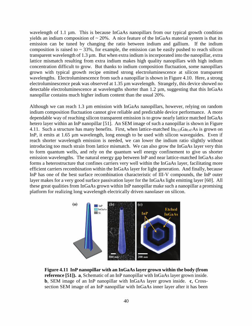
40
wavelength of 1.1 µm. This is because InGaAs nanopillars from our typical growth condition
yields an indium composition of ~ 20%. A nice feature of the InGaAs material system is that its
emission can be tuned by changing the ratio between indium and gallium. If the indium
composition is raised to ~ 33%, for example, the emission can be easily pushed to reach silicon
transparent wavelength of 1.3 µm. But when extra indium is incorporated into the nanopillar, extra
lattice mismatch resulting from extra indium makes high quality nanopillars with high indium
concentration difficult to grow. But thanks to indium composition fluctuation, some nanopillars
grown with typical growth recipe emitted strong electroluminescence at silicon transparent
wavelengths. Electroluminescence from such a nanopillar is shown in Figure 4.10. Here, a strong
electroluminescence peak was observed at 1.35 µm wavelength. Strangely, this device showed no
detectable electroluminescence at wavelengths shorter than 1.2 µm, suggesting that this InGaAs
nanopillar contains much higher indium content than the usual 20%.
Although we can reach 1.3 µm emission with InGaAs nanopillars, however, relying on random
indium composition fluctuation cannot give reliable and predictable device performance. A more
dependable way of reaching silicon transparent emission is to grow nearly lattice matched InGaAs
hetero layer within an InP nanopillar [51]. An SEM image of such a nanopillar is shown in Figure
4.11. Such a structure has many benefits. First, when lattice-matched In0.53Ga0.47As is grown on
InP, it emits at 1.65 µm wavelength, long enough to be used with silicon waveguides. Even if
reach shorter wavelength emission is needed, we can lower the indium ratio slightly without
introducing too much strain from lattice mismatch. We can also grow the InGaAs layer very thin
to form quantum wells, and rely on the quantum well energy confinement to give us shorter
emission wavelengths. The natural energy gap between InP and near lattice-matched InGaAs also
forms a heterostructure that confines carriers very well within the InGaAs layer, facilitating more
efficient carriers recombination within the InGaAs layer for light generation. And finally, because
InP has one of the best surface recombination characteristic of III-V compounds, the InP outer
layer makes for a very good surface passivation layer for the InGaAs light emitting layer [60]. All
these great qualities from InGaAs grown within InP nanopillar make such a nanopillar a promising
platform for realizing long wavelength electrically driven nanolaser on silicon.
Figure 4.11 InP nanopillar with an InGaAs layer grown within the body (from
reference [51]). a, Schematic of an InP nanopillar with InGaAs layer grown inside.
b, SEM image of an InP nanopillar with InGaAs layer grown inside. c, Cross-
section SEM image of an InP nanopillar with InGaAs inner layer after it has been

41
etched with an etchant that selectively etches away InGaAs. The etched InGaAs
layer shows that there is indeed an InGaAs layer within the InP nanopillar.
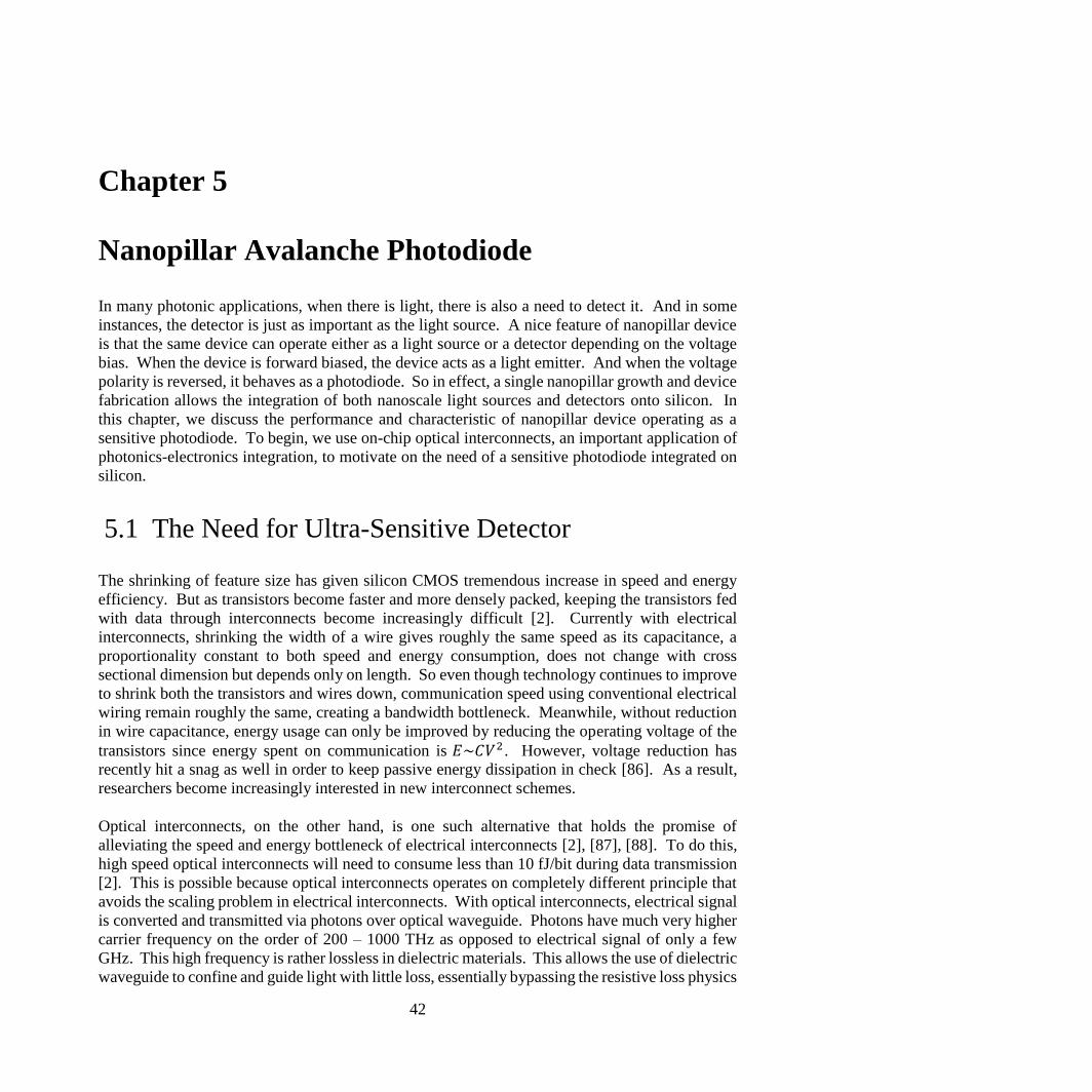
42
Chapter 5
Nanopillar Avalanche Photodiode
In many photonic applications, when there is light, there is also a need to detect it. And in some
instances, the detector is just as important as the light source. A nice feature of nanopillar device
is that the same device can operate either as a light source or a detector depending on the voltage
bias. When the device is forward biased, the device acts as a light emitter. And when the voltage
polarity is reversed, it behaves as a photodiode. So in effect, a single nanopillar growth and device
fabrication allows the integration of both nanoscale light sources and detectors onto silicon. In
this chapter, we discuss the performance and characteristic of nanopillar device operating as a
sensitive photodiode. To begin, we use on-chip optical interconnects, an important application of
photonics-electronics integration, to motivate on the need of a sensitive photodiode integrated on
silicon.
5.1 The Need for Ultra-Sensitive Detector
The shrinking of feature size has given silicon CMOS tremendous increase in speed and energy
efficiency. But as transistors become faster and more densely packed, keeping the transistors fed
with data through interconnects become increasingly difficult [2]. Currently with electrical
interconnects, shrinking the width of a wire gives roughly the same speed as its capacitance, a
proportionality constant to both speed and energy consumption, does not change with cross
sectional dimension but depends only on length. So even though technology continues to improve
to shrink both the transistors and wires down, communication speed using conventional electrical
wiring remain roughly the same, creating a bandwidth bottleneck. Meanwhile, without reduction
in wire capacitance, energy usage can only be improved by reducing the operating voltage of the
transistors since energy spent on communication is 𝐸~𝐶𝑉2 . However, voltage reduction has
recently hit a snag as well in order to keep passive energy dissipation in check [86]. As a result,
researchers become increasingly interested in new interconnect schemes.
Optical interconnects, on the other hand, is one such alternative that holds the promise of
alleviating the speed and energy bottleneck of electrical interconnects [2], [87], [88]. To do this,
high speed optical interconnects will need to consume less than 10 fJ/bit during data transmission
[2]. This is possible because optical interconnects operates on completely different principle that
avoids the scaling problem in electrical interconnects. With optical interconnects, electrical signal
is converted and transmitted via photons over optical waveguide. Photons have much very higher
carrier frequency on the order of 200 – 1000 THz as opposed to electrical signal of only a few
GHz. This high frequency is rather lossless in dielectric materials. This allows the use of dielectric
waveguide to confine and guide light with little loss, essentially bypassing the resistive loss physics

43
that metal wire has. The high carrier frequency of photons also allows signal modulation speed
much faster than electrical signal without introducing much signal distortion. And since photons
are detected quantum mechanically, a voltage close to the photon energy can be recovered at the
receiver even with just a few femto joules of optical pulse [2]. Such high voltage recovery from
such low energy signal is rather important since operating voltage down scaling of CMOS
transistors is ceasing [86]. As such, it is this attribute that allows optical interconnects to beat the
energy usage of electrical interconnects.
Figure 5.1 Schematic of an optical interconnect.
The key to low energy per bit operation in optical interconnects lies within the photo-detector.
When photons arrive at the detector, the photons are converted into electron-hole pairs. These
carriers charge up the photo-detector and input transistor capacitors, giving rise to a photo-voltage.
Since the amount of voltage depends inversely to the capacitance (𝑉~𝑄
𝐶), making the detector
faster and more sensitive means reducing the capacitance of the detector and input transistor.
Currently, CMOS technology at the 32 nm node has input capacitance of 380 aF [2]. Couple this
to a micron size photo-detector, the total capacitance would only be a few femto farads. Therefore,
assuming that every photon is absorbed, a ~ 1 V signal, which is the full logic voltage swing in
CMOS transistor, can be recovered at the input transistor with just a few femto joules of 1 eV
optical signal (equivalent to a few thousands photons).
The exciting new possibilities of optical interconnects have led researchers on a quest to build
photo-detectors for this very purpose. Some build detectors completely out of CMOS transistors
and diodes [89]. But such detectors can only detect light that is absorbable in silicon, making the
use of silicon waveguides impossible. Others circumvent this limitation by using germanium as
the absorbing material [90]–[103]. With optimization, germanium detectors with capacitance in
the range of 1-10 pF have even been integrated onto silicon waveguides [91], [93], [95], [96], [99],
[100].
Often times, reducing capacitance means reducing the size of the detector. But at the same time,
the detector cannot be made too small, or else the detector may not be able to absorb all the light.
For this reason, even though germanium detectors have been shown to have capacitance in the
range of 1-10 pF, however, these detectors are several microns big and have trouble scaling to sub-
pico farad capacitance range. While the use of antennae certainly helps enhancing light absorption
and miniaturizing the detector area and capacitance [103], [104], the detector should be made with
material that has the highest absorption coefficient possible, such as III-V compounds, so that the
detector can be made as small as possible. However, for reasons mentioned in Chapter 2, III-V
compounds have incompatibilities with silicon, which makes using III-V compounds as optical
Driver
Waveguide
Cpd
Receiver
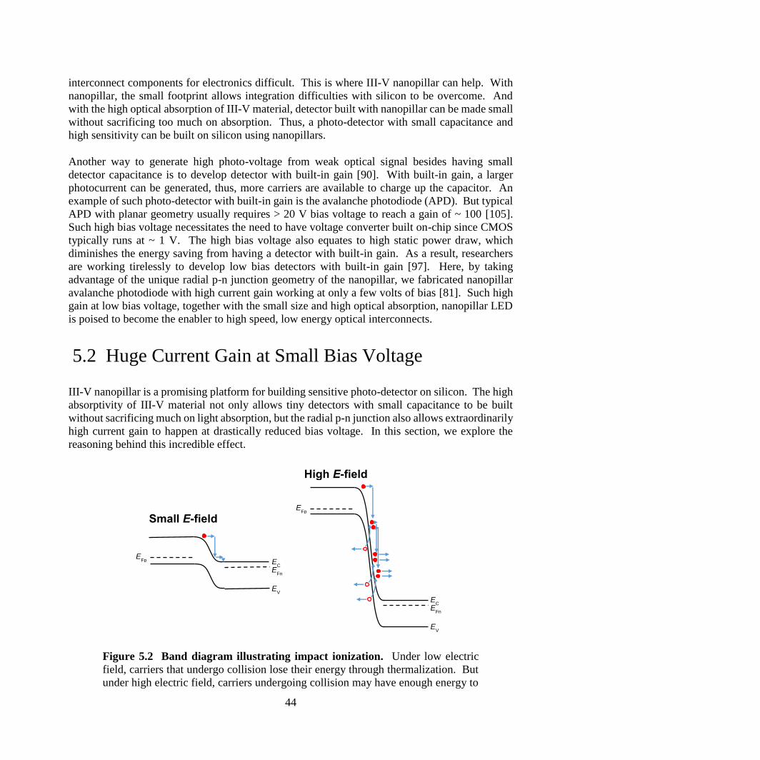
44
interconnect components for electronics difficult. This is where III-V nanopillar can help. With
nanopillar, the small footprint allows integration difficulties with silicon to be overcome. And
with the high optical absorption of III-V material, detector built with nanopillar can be made small
without sacrificing too much on absorption. Thus, a photo-detector with small capacitance and
high sensitivity can be built on silicon using nanopillars.
Another way to generate high photo-voltage from weak optical signal besides having small
detector capacitance is to develop detector with built-in gain [90]. With built-in gain, a larger
photocurrent can be generated, thus, more carriers are available to charge up the capacitor. An
example of such photo-detector with built-in gain is the avalanche photodiode (APD). But typical
APD with planar geometry usually requires > 20 V bias voltage to reach a gain of ~ 100 [105].
Such high bias voltage necessitates the need to have voltage converter built on-chip since CMOS
typically runs at ~ 1 V. The high bias voltage also equates to high static power draw, which
diminishes the energy saving from having a detector with built-in gain. As a result, researchers
are working tirelessly to develop low bias detectors with built-in gain [97]. Here, by taking
advantage of the unique radial p-n junction geometry of the nanopillar, we fabricated nanopillar
avalanche photodiode with high current gain working at only a few volts of bias [81]. Such high
gain at low bias voltage, together with the small size and high optical absorption, nanopillar LED
is poised to become the enabler to high speed, low energy optical interconnects.
5.2 Huge Current Gain at Small Bias Voltage
III-V nanopillar is a promising platform for building sensitive photo-detector on silicon. The high
absorptivity of III-V material not only allows tiny detectors with small capacitance to be built
without sacrificing much on light absorption, but the radial p-n junction also allows extraordinarily
high current gain to happen at drastically reduced bias voltage. In this section, we explore the
reasoning behind this incredible effect.
Figure 5.2 Band diagram illustrating impact ionization. Under low electric
field, carriers that undergo collision lose their energy through thermalization. But
under high electric field, carriers undergoing collision may have enough energy to
EC
EFn
EV
EFp
High E-field
EC
EFn
EV
EFp
Small E-field

45
cause bound carriers to become unbound. These newly created carriers may
undertake the same process to create more free carriers, creating what is known as
avalanche breakdown in a diode.
When a diode is under low reverse bias, there is usually very little current flowing through the
device. But under high reverse bias voltage, the electric field inside depletion region of the device
may become large enough to accelerate carriers to an extremely high speed. For example, when
an electron traveling at high speed collide with another electron at a bound state, the high speed
collision may have enough energy to promote the bound electron to the unbound state in the
conduction band, leaving behind an electron-hole pair. Such a process is illustrated in Figure 5.2
and it is called impact ionization. The newly created electron and hole may also get accelerated
by the high electric field to acquire high enough energy to cause further impact ionization. Such
cascading effect is what leads to avalanche breakdown in the diode.
When used as a detector, the avalanche breakdown effect creates a cascading carrier multiplication
effect, turning tiny photocurrent into much larger one to improve detector responsivity. Avalanche
breakdown in planar geometry typically happens at > 20 V reverse bias [105]. But when the p-n
junction is wrapped in a cylindrical geometry, such as that found in a nanopillar device, the
curvature of the junction enhances electric field within the depletion region, allowing avalanche
breakdown to happen at a drastically reduced bias voltage [106]. Baliga and Ghandhi in reference
[106] found that the amount of breakdown voltage reduction largely depends on the ratio between
junction radius of curvature and depletion width. Since our nanopillar has radius of curvature
ranging from 3 to 300 nm and a calculated depletion width of ~ 1 µm, the breakdown voltage in
nanopillar is expected to be around 5% to 50% of that in planar geometry. The natural core-shell
formation of nanopillar offers a controllable way to design and fabricate cylindrical p-n junction
for APD with much reduced bias voltage.
To verify that nanopillar can indeed have concentrated electric field greater than required for
avalanche to happen, we used commercial 3-D multi-physics device simulation tool Sentaurus to
find out. Figure 5.3 shows the GaAs nanopillar device structure that was simulated. The metal
contacts were set up as voltage boundary conditions in the simulation. The n- and p- layers had
doping concentration of 1.2 × 1017 cm-3 and 1018 cm-3, respectively. The spin-on-glass (SOG)
layer was treated as silicon dioxide in the simulation tool. Electric field calculation was then
performed by solving Poisson’s equation iteratively.
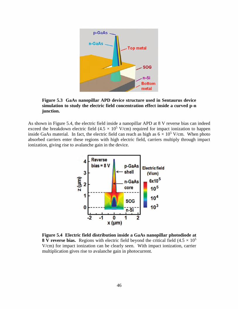
46
Figure 5.3 GaAs nanopillar APD device structure used in Sentaurus device
simulation to study the electric field concentration effect inside a curved p-n
junction.
As shown in Figure 5.4, the electric field inside a nanopillar APD at 8 V reverse bias can indeed
exceed the breakdown electric field (4.5 × 10⁵ V/cm) required for impact ionization to happen
inside GaAs material. In fact, the electric field can reach as high as 6 × 10⁵ V/cm. When photo
absorbed carriers enter these regions with high electric field, carriers multiply through impact
ionization, giving rise to avalanche gain in the device.
Figure 5.4 Electric field distribution inside a GaAs nanopillar photodiode at
8 V reverse bias. Regions with electric field beyond the critical field (4.5 × 10⁵
V/cm) for impact ionization can be clearly seen. With impact ionization, carrier
multiplication gives rise to avalanche gain in photocurrent.
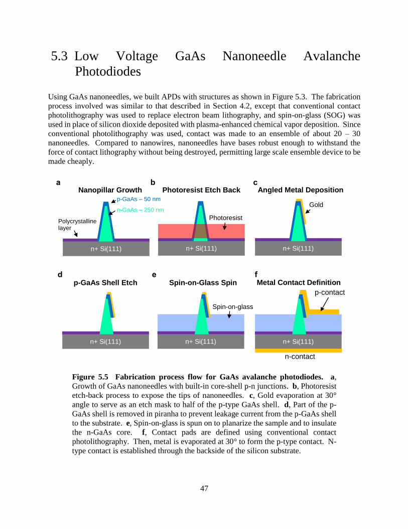
47
5.3 Low Voltage GaAs Nanoneedle Avalanche
Photodiodes
Using GaAs nanoneedles, we built APDs with structures as shown in Figure 5.3. The fabrication
process involved was similar to that described in Section 4.2, except that conventional contact
photolithography was used to replace electron beam lithography, and spin-on-glass (SOG) was
used in place of silicon dioxide deposited with plasma-enhanced chemical vapor deposition. Since
conventional photolithography was used, contact was made to an ensemble of about 20 – 30
nanoneedles. Compared to nanowires, nanoneedles have bases robust enough to withstand the
force of contact lithography without being destroyed, permitting large scale ensemble device to be
made cheaply.
Figure 5.5 Fabrication process flow for GaAs avalanche photodiodes. a,
Growth of GaAs nanoneedles with built-in core-shell p-n junctions. b, Photoresist
etch-back process to expose the tips of nanoneedles. c, Gold evaporation at 30°
angle to serve as an etch mask to half of the p-type GaAs shell. d, Part of the p-
GaAs shell is removed in piranha to prevent leakage current from the p-GaAs shell
to the substrate. e, Spin-on-glass is spun on to planarize the sample and to insulate
the n-GaAs core. f, Contact pads are defined using conventional contact
photolithography. Then, metal is evaporated at 30° to form the p-type contact. N-
type contact is established through the backside of the silicon substrate.
Polycrystalline layer
n+ Si(111)
p-GaAs – 50 nm
n+ Si(111)
Nanopillar Growth
n+ Si(111)
n+ Si(111)
Photoresist Etch Back Angled Metal Deposition
p-GaAs Shell Etch Spin-on-Glass Spin Metal Contact Definition
n-GaAs – 250 nm
a b c
d e f
n+ Si(111) n+ Si(111)
p-contact
n-contact
Photoresist
Spin-on-glass
Gold
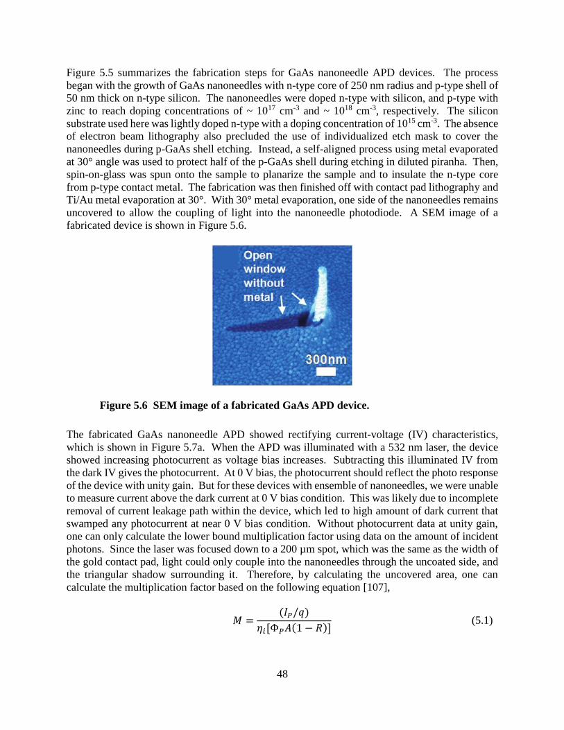
48
Figure 5.5 summarizes the fabrication steps for GaAs nanoneedle APD devices. The process
began with the growth of GaAs nanoneedles with n-type core of 250 nm radius and p-type shell of
50 nm thick on n-type silicon. The nanoneedles were doped n-type with silicon, and p-type with
zinc to reach doping concentrations of ~ 1017 cm-3 and ~ 1018 cm-3, respectively. The silicon
substrate used here was lightly doped n-type with a doping concentration of 1015 cm-3. The absence
of electron beam lithography also precluded the use of individualized etch mask to cover the
nanoneedles during p-GaAs shell etching. Instead, a self-aligned process using metal evaporated
at 30° angle was used to protect half of the p-GaAs shell during etching in diluted piranha. Then,
spin-on-glass was spun onto the sample to planarize the sample and to insulate the n-type core
from p-type contact metal. The fabrication was then finished off with contact pad lithography and
Ti/Au metal evaporation at 30°. With 30° metal evaporation, one side of the nanoneedles remains
uncovered to allow the coupling of light into the nanoneedle photodiode. A SEM image of a
fabricated device is shown in Figure 5.6.
Figure 5.6 SEM image of a fabricated GaAs APD device.
The fabricated GaAs nanoneedle APD showed rectifying current-voltage (IV) characteristics,
which is shown in Figure 5.7a. When the APD was illuminated with a 532 nm laser, the device
showed increasing photocurrent as voltage bias increases. Subtracting this illuminated IV from
the dark IV gives the photocurrent. At 0 V bias, the photocurrent should reflect the photo response
of the device with unity gain. But for these devices with ensemble of nanoneedles, we were unable
to measure current above the dark current at 0 V bias condition. This was likely due to incomplete
removal of current leakage path within the device, which led to high amount of dark current that
swamped any photocurrent at near 0 V bias condition. Without photocurrent data at unity gain,
one can only calculate the lower bound multiplication factor using data on the amount of incident
photons. Since the laser was focused down to a 200 µm spot, which was the same as the width of
the gold contact pad, light could only couple into the nanoneedles through the uncoated side, and
the triangular shadow surrounding it. Therefore, by calculating the uncovered area, one can
calculate the multiplication factor based on the following equation [107],
𝑀 =
(𝐼𝑃/𝑞)
𝜂𝑖[Φ𝑃𝐴(1 − 𝑅)] (5.1)

49
where 𝐼𝑃 , 𝑞 , ηi , Φ𝑃 , 𝐴 and 𝑅 are photocurrent, electron charge, internal quantum efficiency,
incident photon flux (estimated from exposed area) and device reflectivity, respectively. The
numerator, 𝐼𝑃/𝑞 , is simply the number of electrons output by the APD per unit time. The
denominator, 𝜂𝑖[Φ𝑃𝐴(1 − 𝑅)], is the number of collected photons per unit time. So by dividing
the two, we get the ratio of output electrons versus input photons, which is the multiplication factor.
Assuming 100% internal quantum efficiency, we can calculate the lower bound of multiplication
factor experimentally observed with equation (5.1 by plugging in the measured photocurrent and
calculated reflectivity from the SOG/silicon interface. The experimental lower bound
multiplication factor is plotted in Figure 5.7b. As shown, the multiplication factor can be as high
as 100 with only 4 V reverse bias, and can reach ~ 263 at 8 V bias. In contrast, it takes a planar
InGaAs/silicon APD 24 V to reach a gain of 100 [105]. The much reduced bias voltage to reach
sizeable avalanche gain is especially compelling for low energy optical interconnects application
as it can drastically reduce the static power draw necessary to bias the detector. In addition, the
observed gain has a much more linear relationship with bias voltage, as opposed to the exponential
relationship typically found in conventional APD [107]. This rather linear behavior is
advantageous in achieving stable device operation and avoiding device burn-out.
Figure 5.7 GaAs nanopillar APD device performance. a, Current-voltage (IV)
characteristics of a GaAs nanopillar APD tested under dark and illuminated
condition. The photocurrent of the device increases as bias voltage increases,
which is a sign of gain in the device. b, Lower bound multiplication factor for
device shown in (a).
Another interesting effect that arises from the nanoneedle geometry is the collection of carriers
generated in silicon even when the illumination is far away from the p-n junction. The
photocurrent data shown in Figure 5.7 tells the story. With the photodiode biased at -10 V and
illuminated with a 980 nm laser, we continued to measure photocurrent even when the laser light
is below the band gap of the GaAs nanoneedle. This observation suggests that the silicon substrate
also participates in photon absorption. As the incident laser beam was moved away from the
nanoneedle photodiodes contacts and into the silicon substrate, as stylized in Figure 5.8, we
continue to observe measurable amount of photocurrent. Since there are no connected nanoneedles
a b
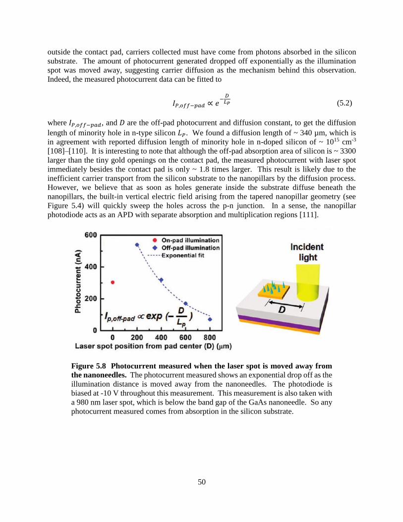
50
outside the contact pad, carriers collected must have come from photons absorbed in the silicon
substrate. The amount of photocurrent generated dropped off exponentially as the illumination
spot was moved away, suggesting carrier diffusion as the mechanism behind this observation.
Indeed, the measured photocurrent data can be fitted to
𝐼𝑃,𝑜𝑓𝑓−𝑝𝑎𝑑 ∝ 𝑒
−𝐷𝐿𝑃 (5.2)
where 𝐼𝑃,𝑜𝑓𝑓−𝑝𝑎𝑑, and 𝐷 are the off-pad photocurrent and diffusion constant, to get the diffusion
length of minority hole in n-type silicon 𝐿𝑃. We found a diffusion length of ~ 340 µm, which is
in agreement with reported diffusion length of minority hole in n-doped silicon of ~ 1015 cm-3
[108]–[110]. It is interesting to note that although the off-pad absorption area of silicon is ~ 3300
larger than the tiny gold openings on the contact pad, the measured photocurrent with laser spot
immediately besides the contact pad is only ~ 1.8 times larger. This result is likely due to the
inefficient carrier transport from the silicon substrate to the nanopillars by the diffusion process.
However, we believe that as soon as holes generate inside the substrate diffuse beneath the
nanopillars, the built-in vertical electric field arising from the tapered nanopillar geometry (see
Figure 5.4) will quickly sweep the holes across the p-n junction. In a sense, the nanopillar
photodiode acts as an APD with separate absorption and multiplication regions [111].
Figure 5.8 Photocurrent measured when the laser spot is moved away from
the nanoneedles. The photocurrent measured shows an exponential drop off as the
illumination distance is moved away from the nanoneedles. The photodiode is
biased at -10 V throughout this measurement. This measurement is also taken with
a 980 nm laser spot, which is below the band gap of the GaAs nanoneedle. So any
photocurrent measured comes from absorption in the silicon substrate.
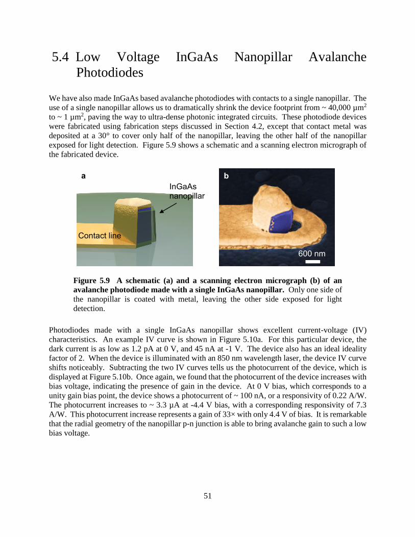
51
5.4 Low Voltage InGaAs Nanopillar Avalanche
Photodiodes
We have also made InGaAs based avalanche photodiodes with contacts to a single nanopillar. The
use of a single nanopillar allows us to dramatically shrink the device footprint from ~ 40,000 µm2
to ~ 1 µm2, paving the way to ultra-dense photonic integrated circuits. These photodiode devices
were fabricated using fabrication steps discussed in Section 4.2, except that contact metal was
deposited at a 30° to cover only half of the nanopillar, leaving the other half of the nanopillar
exposed for light detection. Figure 5.9 shows a schematic and a scanning electron micrograph of
the fabricated device.
Figure 5.9 A schematic (a) and a scanning electron micrograph (b) of an
avalanche photodiode made with a single InGaAs nanopillar. Only one side of
the nanopillar is coated with metal, leaving the other side exposed for light
detection.
Photodiodes made with a single InGaAs nanopillar shows excellent current-voltage (IV)
characteristics. An example IV curve is shown in Figure 5.10a. For this particular device, the
dark current is as low as 1.2 pA at 0 V, and 45 nA at -1 V. The device also has an ideal ideality
factor of 2. When the device is illuminated with an 850 nm wavelength laser, the device IV curve
shifts noticeably. Subtracting the two IV curves tells us the photocurrent of the device, which is
displayed at Figure 5.10b. Once again, we found that the photocurrent of the device increases with
bias voltage, indicating the presence of gain in the device. At 0 V bias, which corresponds to a
unity gain bias point, the device shows a photocurrent of ~ 100 nA, or a responsivity of 0.22 A/W.
The photocurrent increases to ~ 3.3 µA at -4.4 V bias, with a corresponding responsivity of 7.3
A/W. This photocurrent increase represents a gain of 33× with only 4.4 V of bias. It is remarkable
that the radial geometry of the nanopillar p-n junction is able to bring avalanche gain to such a low
bias voltage.
InGaAs nanopillar
Contact line
a
600 nm
b

52
Figure 5.10 InGaAs nanopillar avalanche photodiode device characteristics.
a, Current-voltage (IV) behavior. b, Photocurrent and gain of the device.
The avalanche photodiode is also capable of high speed operation. Figure 5.11 displays the S21
response curve of the device taken at 4.4 V bias. The response curve shows a 3 dB bandwidth of
3.1 GHz, suggesting that a gain-bandwidth product as much as 102 GHz is achieved. Although
the high speed performance of the device is still some distance away from the state-of-the-art
planar counterparts [90], [97], our current generation devices are not optimized for electrical
parasitic capacitance from the device contacts. We believe performance on par with state-of-the-
art devices is entirely achievable through further design and optimization.
Figure 5.11 Frequency response of InGaAs avalanche photodiode. The device
has a 3 dB bandwidth of 3.1 GHz.
5.5 Giant Gain from InP Photodiodes
Sensitive photodiode can also be built using InP nanopillar to take advantage of its low surface
recombination characteristics. The fabrication process is actually much simpler with InP as InP
0.1 1 5
-6
-4
-2
0
2
Resp
on
se (
dB
)
Frequency (GHz)
-4 -2 0 21E-13
1E-12
1E-11
1E-10
1E-9
1E-8
1E-7
1E-6
1E-5
Cu
rren
t (A
)
Voltage (V)
a
Dark
Illuminated
b

53
nanopillar growth does not produce parasitic polycrystalline layer during growth, so the steps
dedicated to the removal of the polycrystalline layer described in Section 4.2 can be skipped.
Figure 5.12 describes the fabrication of InP nanopillar photodiode in details.
Figure 5.12 Fabrication process for InP nanopillar devices. a, Nanopillar
structure after growth. b, Alignment marks are laid down just after growth using
electron beam lithography to help locate the nanopillars. c, Alignment marks metal
evaporation and nanopillar location registration. d, Silicon dioxide is deposited via
plasma enhanced chemical vapor deposition. This silicon dioxide layer electrically
isolates the substrate from the top contact metal that is to be deposited. e, f, A
photoresist etch back process is used to expose the tip of the nanopillar. g, Electron
beam lithography to define contact to individual nanopillar. h, Metal is deposited
to both top and bottom of the wafer to complete the fabrication.
p+ Si(111)
n-InP – 70 nm
p+ Si(111)
Nanopillar Growth
p+ Si(111)
p+ Si(111)
Alignment Mark Lithography Alignment Mark Evaporation
SiO2 Electrical Isolation Photoresist Etch Back Expose Tip for Contact
p-InP – 330 nm
a b c
d e f
p+ Si(111) p+ Si(111)
p+ Si(111)
Contact Pad Lithography Metal Contact Deposition g h
p+ Si(111)
Photoresist
Photoresist
SiO2
Alignment mark
Photoresist n-contact
p-contact
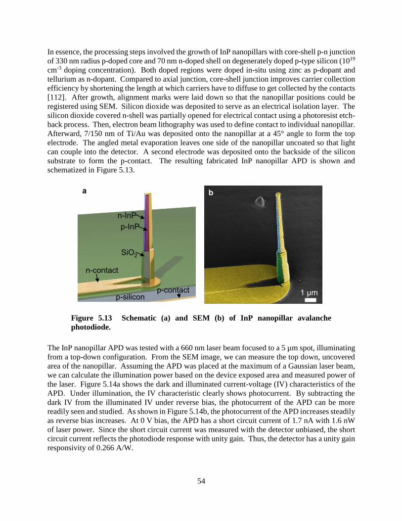
54
In essence, the processing steps involved the growth of InP nanopillars with core-shell p-n junction
of 330 nm radius p-doped core and 70 nm n-doped shell on degenerately doped p-type silicon (1019
cm-3 doping concentration). Both doped regions were doped in-situ using zinc as p-dopant and
tellurium as n-dopant. Compared to axial junction, core-shell junction improves carrier collection
efficiency by shortening the length at which carriers have to diffuse to get collected by the contacts
[112]. After growth, alignment marks were laid down so that the nanopillar positions could be
registered using SEM. Silicon dioxide was deposited to serve as an electrical isolation layer. The
silicon dioxide covered n-shell was partially opened for electrical contact using a photoresist etch-
back process. Then, electron beam lithography was used to define contact to individual nanopillar.
Afterward, 7/150 nm of Ti/Au was deposited onto the nanopillar at a 45° angle to form the top
electrode. The angled metal evaporation leaves one side of the nanopillar uncoated so that light
can couple into the detector. A second electrode was deposited onto the backside of the silicon
substrate to form the p-contact. The resulting fabricated InP nanopillar APD is shown and
schematized in Figure 5.13.
Figure 5.13 Schematic (a) and SEM (b) of InP nanopillar avalanche
photodiode.
The InP nanopillar APD was tested with a 660 nm laser beam focused to a 5 µm spot, illuminating
from a top-down configuration. From the SEM image, we can measure the top down, uncovered
area of the nanopillar. Assuming the APD was placed at the maximum of a Gaussian laser beam,
we can calculate the illumination power based on the device exposed area and measured power of
the laser. Figure 5.14a shows the dark and illuminated current-voltage (IV) characteristics of the
APD. Under illumination, the IV characteristic clearly shows photocurrent. By subtracting the
dark IV from the illuminated IV under reverse bias, the photocurrent of the APD can be more
readily seen and studied. As shown in Figure 5.14b, the photocurrent of the APD increases steadily
as reverse bias increases. At 0 V bias, the APD has a short circuit current of 1.7 nA with 1.6 nW
of laser power. Since the short circuit current was measured with the detector unbiased, the short
circuit current reflects the photodiode response with unity gain. Thus, the detector has a unity gain
responsivity of 0.266 A/W.
n-InP
p-InP
p-contact
n-contact
p-silicon
SiO2
a
1 µm
b

55
As shown in Figure 5.14b, as the bias voltage increases, the measured photocurrent increases
rapidly. At 1 V bias, the photocurrent increases to ~ 170 nA, and the responsivity reaches 26.6
A/W. Dividing this photocurrent by the short circuit current gives the gain of the detector at 100.
This is much higher than the gain of 9.3 at 1.5 V bias observed in the state-of-the-art germanium
nano APD integrated onto silicon [97]. Such high gain at such low bias voltage is achievable only
through the core-shell, radial p-n junction of the APD. With a radial p-n junction, the circular
geometry concentrates electric field to the junction area, allowing the device to reach avalanche
condition at a much lower bias voltage [106]. With such high responsivity at such low bias, InP
nanowire APD can potentially enable optical interconnects with extremely low photo/bit energy
operation.
Figure 5.14 InP nanopillar avalanche photodiode device characteristics. a, IV
curves of InP nanowire APD under dark and 1.6 nW laser excitation at 660 nm
wavelength. b, Photocurrent/gain as a function of bias voltage for the APD. With
just 1 V bias, the InP nanowire APD is able to reach a gain of 100.
Unlike APDs made with GaAs, we observed no photocurrent contribution from the silicon
substrate. When we illuminated the device with a 980 nm laser light of significant power, we
measured no detectable photocurrent. Since 980 nm is only absorbable in silicon, the lack
photocurrent shows that silicon does not participate in photo carrier generation. Another proof for
the lack of silicon substrate contribution is the lack of photo response when the 660 nm laser spot
was moved away from the detector. As shown in Figure 5.15, the photocurrent drops to nothing
as soon as the laser spot was moved away from the nanopillar detector by ~ 3 µm. Such
observation is consistent with a 5 µm big laser spot size. Therefore, our assumption of absorption
happening solely within the uncovered portion of the nanopillar is valid. We believe the lack of
silicon contribution here is due two reasons. First, the silicon substrate that was used in the InP
APD experiment was doped to a doping concentration of 1019 cm-3, as opposed to a doping
concentration of 1015 cm-3 for the silicon substrate used in the GaAs APDs. This much higher
doping concentration shortens the diffusion length of minority electron in the degenerately p-
doped silicon substrate a great deal. At a doping concentration of 1019 cm-3, the diffusion length
of minority electron is only ~ 3 µm [113], [114], which pales in comparison to the ~ 340 µm
diffusion length of minority hole observed with the lightly doped silicon substrate used in the GaAs
a b

56
APDs. Such shortened diffusion length likely makes capturing of generated carriers in silicon
much harder. Second, during GaAs nanoneedle growth, there is also a polycrystalline GaAs layer
that was deposited onto the silicon substrate. But for InP nanopillar growth, this layer does not
exist. The presence of this polycrystalline GaAs layer may have contributed to the photocurrent
measurement when the laser spot was moved away from the nanoneedles.
Figure 5.15 InP nanopillar avalanche photodiode shows no photocurrent
when the laser spot is moved away from the center of the nanopillar device. In
fact, the photocurrent drops off to 0 A as soon as the laser spot is moved 3 µm away,
which is consistent with a 5 µm laser spot size. The schematic on the right shows
how the distance in the plot on the right is defined.
Distance
Laser spot
57
Chapter 6
Nanopillar Phototransistor
In Chapter 5, we present three sensitive nanopillar photodiodes with built-in gain. These
photodiodes show high current gain at bias voltage of only a few volts. The high current allows
detection of small signal while the low voltage bias cuts down on static power draw. Although
these attributes are great for low energy on-chip optical interconnects application, but we can do
better. In this chapter, we discuss a new type of detector based on nanopillar that is even better
suited for low energy optical interconnects application. This detector is nanopillar phototransistor.
In the following sections, we first motivate on the phototransistor design. Then, we discuss a novel
growth technique that we developed to make such a phototransistor design possible. We then
show device characteristics, and close the chapter by discussing on ways to improve the
phototransistor design.
6.1 Phototransistor to Reduce Energy/Bit Further
As discussed in detail in Section 5.1, optical interconnects can potentially solve the energy and
bandwidth bottleneck of electrical interconnects. Optical interconnects solves these bottlenecks
by communicating through photons to bypass the resistive loss physics that prevents energy and
bandwidth scaling in electrical interconnects. With photons, even at energy per bit as low as a few
femto joules, a voltage close to the CMOS operating voltage can be recovered [2]. This miraculous
phenomenon essentially forms the basis for optical interconnects.
To recover as high voltage as possible from a small optical signal, the detector needs to be
extremely sensitive. This means the detector needs to have small capacitance and high
photocurrent output since the photo-voltage recovered is 𝑉~𝑄
𝐶. In Chapter 5, we present three
avalanche photodiodes that produce high photocurrent gain with very small bias voltage. The high
current gain helps boost voltage by increasing the amount of coulomb charges available to charge
the capacitors at the photodiode, transistor and wire. While such photodiode design may suffice,
however, we can do better. With photodiode and transistor capacitance at femto and sub-femto
farads, even the ~ 0.2 fF/µm capacitance of the wire connecting the photodiode and transistor starts
becoming significant [2]. And especially since wire capacitance does not benefit from process
technology scaling, this connecting wire should be eliminated as much as possible. One possible
way of eliminating this wire altogether is to integrate the photodiode and transistor together, hence,
giving rise the design of a phototransistor.
58
In fact, researchers have been looking for ways to use such phototransistor design for optical
interconnects purpose [94], [100], [102], [115]. Here we present our phototransistor
implementation using InP nanopillars grown on silicon. With InP nanopillars, the small footprint
and high absorption coefficient makes it a likely candidate for realizing low capacitance, highly
sensitive phototransitor for on-chip optical interconnects application.
6.2 Nanopillar Phototransistor Design and Operation
Turning nanopillar into phototransistor is of no easy task. One must balance design tradeoffs in
fabrication and device characteristics to achieve the best performance possible. Of the two most
common transistor designs, field effect transistor (FET) and bipolar junction transistor (BJT), we
chose to use the BJT design for its relative ease of fabrication and the possibility of using hetero-
junction to further improve device performance. Figure 6.1a and Figure 6.1b shows the schematic
and SEM image of a bipolar junction phototransistor (photo-BJT) made with InP nanopillar. In
this design, the nanopillar has core-shell layers of heavily p-doped shell, moderately n-doped inner
layer, and lightly p-doped core. These three layers form the emitter (shell), base and collector
(core) of a BJT device. Normally in a purely electrically driven BJT, all three layers would have
to be electrically contacted. But since we would like our device to behave as a photo actuated
transistor, the base is left floating and unconnected. Therefore, only the emitter shell and collector
core need to be electrically contacted. With this design, the fabrication process boils down to the
same set of processing steps as the single nanopillar avalanche photodiode, which is described in
detail in Section 5.5. This elegant design dramatically cut down on time and resources spent on
process development.
Figure 6.1 Schematics and scanning electron micrograph of single InP
nanopillar bipolar junction phototransistor fabricated on silicon substrate. a,
3-D schematic of the device. b, Cross-section schematic. The device consists of
p-doped emitter outer shell, n-doped base in the middle, and p-doped collector core.
c, Scanning electron micrograph of a fabricated device.
To understand how a floating base BJT work, consider the band diagrams for a 1-D photo-BJT
shown in Figure 6.2. Figure 6.2a shows a sketch of the band structure when the photo-BJT is not
collector contact
n-base p-emitter
p-collector
SiO2
emitter contact
p-silicon
a
SiO2 Collector: p-InP, 500 nm
Silicon
Base: n-InP, 150 nm
Emitter: p-InP, 100 nm
Emitter Contact
Collector Contact
b
1 µm
c
59
illuminated, but under slight voltage bias across the emitter-collector terminals, defined as shown
in Figure 6.2c. Since the collector is usually very lightly doped compared to the other two regions,
much of the bias voltage is dropped across the base-collector junction [110]. The doping profile
of the device also forms a potential barrier for holes and electrons to move across the base. As a
result, there is very little collector current. When the device is illuminated with a light source,
because of the presence of the electronic barrier, electrons starts accumulating at the base. This
accumulation of electrons causes the base region Fermi energy to rise, effectively raising the bands
within the base region [116], [117]. This results in a band structure resembling to the one shown
in Figure 6.2b. When this happens, the potential barrier at the base shrinks, allowing thermally
excited holes to diffuse into the base more easily. Since the base is typically sized very thin such
that the quasi-neutral base thickness is less than the diffusion length for holes, most of these
injected holes end up making across to the collector side, where they become majority carriers
again and get collected by the collector contact. Thus, collector current increases under the
actuation of light illumination.
Figure 6.2 Band structure inside a bipolar junction phototransistor. a, Band
diagram of a bipolar junction phototransistor without light illumination, but under
a slight emitter-collector bias. b, Band diagram of a bipolar junction
phototransistor under light illumination. Under illumination, electrons (blue dots)
accumulate at the base, causing a rise in the Fermi energy with the base. This
effectively lowers the potential barrier so that thermally excited holes can get
injected into the base more easily. Most of these injected holes end up making
across to the collector side, thus, increasing the collector current. c, Schematic
illustrating the emitter-collector bias.
Another way to understand the operation of a homo-junction photo-BJT is to think of light
absorption in the base-collection region as creating a base bias current from the photo absorbed
carriers. These absorbed carriers create a base-emitter voltage equivalent to,
𝑉𝐵𝐸 ≈
𝑛𝑘𝑇
𝑞ln (
𝑃𝑖𝑛𝑐𝐼𝑆
𝜂𝑞
ℏ𝜔) (6.1)
where 𝑛, 𝑘, 𝑇, 𝑞, 𝑃𝑖𝑛𝑐, 𝐼𝑆, 𝜂 and ℏ𝜔 are ideality factor, Boltzmann constant, temperature, electron
charge, incident light power, dark current of the emitter-base junction, quantum efficiency and
photon energy, respectively. The term 𝑃𝑖𝑛𝑐𝜂𝑞
ℏ𝜔 is essentially the photocurrent generated by photon
emitter base
collector
p-InP
n-InP
p-InP
No Light
a
emitter base
collector
p-InP
n-InP
p-InP
With Light
b
+ -
emitter base collector
c

60
absorption inside the base-collector region. This photo generated 𝑉𝐵𝐸 biases the base-emitter
region, allowing normal BJT action to happen. Thus, when there is light illumination, collector
current flows.
Visualizing the operation of a photo-BJT as a conventional BJT is a rather powerful insight in
guiding design decision. Equation (6.1 basically tells us that, in order to reach high base-emitter
bias, dark current must be minimized. This leads us to develop a new growth method to regrow
the emitter and base regions only on the top portion of an already grown collector core. This
regrowth method cuts down on dark current drastically, allowing phototransistor action to happen.
In fact, photo-BJT made without this regrowth method shows no transistor action. Thus, regrowth
is absolutely necessary, and it is the enabler to realizing nanopillar photo-BJT. More on the
regrowth process is described in the next section.
Typically in a BJT, the emitter is doped more heavily than the base. This means more hole
diffusion from the emitter to the base happens than electron diffusion from the base to the emitter
[110]. This asymmetry carrier injection is what gives rise to transistor gain. The emitter region
is typically made very thin also, so most of the light absorption can take place across the base-
collector region. This is crucial because the base-collector junction has the biggest depletion
region that collects and redirects carriers into the base to create a potential change. Another
important decision made to the design is placing the collector region at the core of the nanopillar.
This is done because the collector has the lightest doping concentration. If we put it at the shell,
there may not be enough volume for the depletion region to form, which may lead to degraded
device performance.
6.3 Regrowth on InP Nanopillar – Achieving Record Low
Dark Current in Nanowire Devices
As previously mentioned, regrowth is the enabler to realizing nanopillar photo-BJT. But before
we begin describing the regrowth process, let us take a look at the problem without regrowth. If
we just grow the collector, base and emitter layers in a continuous core-shell growth, as shown in
Figure 6.3, the p-doped emitter shell will be directly connected to the p-doped substrate. This
means there will always be a current flowing from the emitter to the collector contact at the
substrate no matter what. To get rid of this shunt current path, one can use the etching technique
described in Section 4.2. We tried that, but photo-BJT devices made with shunt path etching
technique shows no collector current change when light illumination is changed! This is because
it is extremely difficult to completely etch away the entire shunt path without uprooting the
nanopillar. Even if we succeed in etching away the entire shunt path at the bottom, surface states
left behind from etching still leaves a somewhat large amount of dark current, as III-V compounds
are extremely sensitive to surface conditions [48]. In fact, typical dark current of devices made
with shunt path etching technique is still quite high at ~ 100 pA. Under standard testing
illumination power of ~ 1 nW, only ~ 0.1 V is generated at 𝑉𝐵𝐸 (calculated with Equation (6.1).
This is nowhere near enough to bias the photo-BJT. As a result, photo-BJT made made with shunt
path etching technique shows no photo dependent collector current.
61
Figure 6.3 The problem without regrowth. Schematic showing the problem of
shunt current path when the layers of a bipolar junction phototransistor is grown in
one continuous growth. Since the p-doped emitter is touching the p-doped silicon
substrate directly, current always flows between the emitter and collector contacts.
The problem of dark current leads us to the development of regrowth. Instead of growing all the
layers in one single growth, we grew only the light p-doped collector first. Then, we took the
sample out of the MOCVD chamber, and mask the bottom portion of the nanopillar with silicon
dioxide (SiO2) and amorphous silicon prior to regrowth. The two mask layers were deposit in a
plasma-enhanced chemical vapor deposition tool. Amorphous silicon was found to be critical to
aid the regrowth process by shortening the diffusion lengths of the growth precursor adatoms.
Then, photoresist was spun onto the sample and later etched back in O2 plasma to expose the top
portion of the nanopillar. The amorphous silicon and SiO2 on top are etched away in heated
tetramethylammonium hydroxide and 10:1 buffered hydrofluoric acid, respectively. After etching,
the photoresist was removed in heated acetone. Prior to putting the sample back into the MOCVD
for regrowth, the sample was deoxidized in diluted piranha and hydrochloric acid. At this state,
the sample was ready for regrowth in the MOCVD at 450°C to complete the n-doped base and p-
doped emitter shell. Figure 6.4 shows schematically how the regrowth process works.
With regrowth, the size and location of the p-i-n junction can be controlled precisely along the
length of the nanopillar. This added control allows us to lift the emitter and base layers away from
the substrate, cutting off the current leakage path entirely. Figure 6.5 shows the before and after
regrowth scanning electron micrographs, showing the smooth sidewalls of a regrown nanopillar
as a sign of excellent regrowth material quality. Indeed, when examined under transmission
electron microscope (Figure 6.5b), the regrown junction exhibits high crystal quality with no
stacking dislocation throughout large sections of the nanopillars. This shows that the regrown
region is virtually stacking dislocation free.
Collector: p-InP
Base: n-InP
Emitter: p-InP
p-Silicon
Shunt path from p-InP to substrate

62
Figure 6.4 Regrowth on nanopillar. Schematics of a nanopillar before and after
regrowth.
Figure 6.5 Regrowth on nanopillar. a, Scanning electron micrographs of a
nanopillar before and after the regrowth. The regrown layers only grow on the top
portion of the nanopillar because the bottom half of the nanopillar is masked with
an amorphous silicon (a-Si) and SiO2 mask. The zoomed in image on the right
shows the smooth sidewalls of the regrown layers, suggesting that the regrown
1 µm
Before Regrowth After Regrowth
p-InPRegrown
i- and n-
layers
a-Si &
SiO2
500 nm1 µm
Regrown Original core
50 nm
BF-TEM – off-axis along [0001]
50 nm
Regrown Original core
50 nm
Regrown Original corea
b
SiO2
a-Si
p-Silicon
SiO2
After Regrowth
p-InP
n-InP
p-InP
SiO2
a-Si
p-Silicon
SiO2
p-InP
Before Regrowth
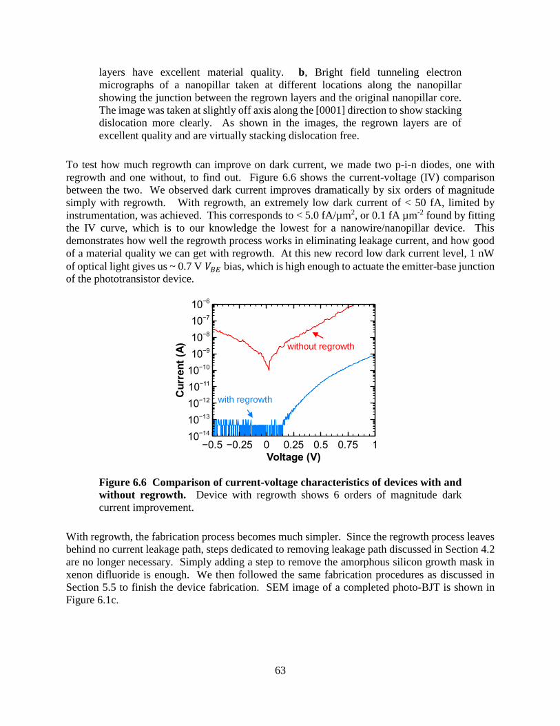
63
layers have excellent material quality. b, Bright field tunneling electron
micrographs of a nanopillar taken at different locations along the nanopillar
showing the junction between the regrown layers and the original nanopillar core.
The image was taken at slightly off axis along the [0001] direction to show stacking
dislocation more clearly. As shown in the images, the regrown layers are of
excellent quality and are virtually stacking dislocation free.
To test how much regrowth can improve on dark current, we made two p-i-n diodes, one with
regrowth and one without, to find out. Figure 6.6 shows the current-voltage (IV) comparison
between the two. We observed dark current improves dramatically by six orders of magnitude
simply with regrowth. With regrowth, an extremely low dark current of < 50 fA, limited by
instrumentation, was achieved. This corresponds to < 5.0 fA/µm2, or 0.1 fA µm-2 found by fitting
the IV curve, which is to our knowledge the lowest for a nanowire/nanopillar device. This
demonstrates how well the regrowth process works in eliminating leakage current, and how good
of a material quality we can get with regrowth. At this new record low dark current level, 1 nW
of optical light gives us ~ 0.7 V 𝑉𝐵𝐸 bias, which is high enough to actuate the emitter-base junction
of the phototransistor device.
Figure 6.6 Comparison of current-voltage characteristics of devices with and
without regrowth. Device with regrowth shows 6 orders of magnitude dark
current improvement.
With regrowth, the fabrication process becomes much simpler. Since the regrowth process leaves
behind no current leakage path, steps dedicated to removing leakage path discussed in Section 4.2
are no longer necessary. Simply adding a step to remove the amorphous silicon growth mask in
xenon difluoride is enough. We then followed the same fabrication procedures as discussed in
Section 5.5 to finish the device fabrication. SEM image of a completed photo-BJT is shown in
Figure 6.1c.
with regrowth
without regrowth

64
6.4 Bipolar Junction Phototransistor in Action
The photo-BJT was tested with 785 nm laser illumination from the side at a 30° angle through a
multi-mode fiber with numerical aperture of 0.27. The fiber was placed 350-400 µm away from
the device, creating a laser spot size of ~ 100 µm wide. By assuming a Gaussian beam profile and
using the photo-BJT dimension measured from SEM, we calibrated the amount of optical power
incident onto the nanopillar photo-BJT. Since the photo-BJT carriers a floating base design, the
photo-BJT is actuated by the photocurrent generated from photon absorption in the base and
collector regions. When not illuminated, the device showed minor collector current for much of
the collector-emitter bias since the p-n junctions inside are reverse biased. But when the device
was illuminated, the photocurrent generated inside the device biases the base in a similar way as
applying a base bias current in a conventional BJT. As a result of this base bias current, the
potential barrier at the emitter-base junction lowers, allowing a finite amount of carriers to flow
freely from the emitter to the collector to form a constant collector current. In a way, this photo-
BJT behaves just like a conventional BJT, except that the base is biased solely through photons.
As such, a characteristic BJT current-voltage (IV) behavior can be clearly seen in Figure 6.7a.
When biased in forward active mode, the photo-BJT shows linear photo response with responsivity
approaching 4 A/W, or a gain of 6.3. Figure 6.7b shows such linear photo response from the
photo-BJT when it is biased with 0.5 V collector bias (Note: collector bias is defined to be the
negative voltage bias on the collector with the respect to the emitter voltage since this is a p-n-p
photo-BJT. Hence, collector bias is equal to the voltage across the emitter-collector junction).
Such linear and sensitive photo-BJT is a promising device in bringing low energy optical
interconnects to silicon electronics.
Figure 6.7 InP nanopillar phototransistor device characteristics. a, Photo-BJT
collector current versus collector voltage at different 785 nm laser excitation. b,
Photo-BJT collector current versus 785 nm laser excitation power curve showing
linear photo response from photo-BJT.
To better understand the device performance, we took the family of collector current versus
collector bias curves and re-plotted it as responsivity versus collector bias. As shown in Figure
a b

65
6.8, responsivity of the device increases with collector bias under saturation regime (between 0 to
0.4 V collector bias), and eventually saturates at 4 A/W at 0.5 V collector bias in forward active
mode. As collector bias continues to increase, responsivity dips. This dip in responsivity is likely
caused by the large amount of Early effect observed in the device since Early effect is known to
reduce gain in conventional BJT devices [110]. We also observed base punch-through at around
0.8 V collector bias, which is a little low. The large amount of Early effect and rather low punch-
through voltage indicate that base width, or base doping concentration, is not quite high enough.
To improve, we can either increase the base width or base doping concentration, but at the cost of
reducing the gain. Though, neither the doping concentration nor thickness of the layers were
optimized in current generation devices. We believe through more thorough device simulation
and design, we will be able to better optimize the design to reach even higher device performance.
Figure 6.8 Responsivity versus collector bias sheds light on device
performance. Responsivity rises as emitter-collector voltage increases until
reaching forward active mode, and eventually peaks at 0.5 V emitter-collector bias.

66
Chapter 7
Illumination Angle Insensitive, High Efficiency
Solar Cell using Single Indium Phosphide
Nanopillar
Lowering the cost of solar energy may accelerate the adoption of solar energy by making it cost
competitive to conventional energy sources. Though, low cost solar cell modules alone cannot
make solar energy cheap enough as module cost accounts for merely half the entire system cost.
The second half of the system cost, which includes installation and infrastructure costs, is actually
shown to be inversely proportional to the efficiency of the solar cell [118]. Therefore, a more
effective approach in reducing the cost of solar energy involves low cost solar cell design that also
boost photovoltaic conversion efficiency. Nanowire or nanopillar based solar cell, as it turns out,
is a promising candidate as it can be made highly efficient and low cost.
7.1 Introduction to Nanowire/Nanopillar Solar Cells
High efficiency solar cells have typically been made with III-V materials because of their high
absorption coefficients and the ability to passivate the surface with hetero-junctions [119]. But
typical growth methods of III-V materials require the use of expensive III-V substrates, which
makes III-V solar cells too costly for widespread adoption. One way of lowering cost while
maintaining the III-V advantages is to make III-V nanowire solar cells [57], [120]–[122] directly
on cheaper foreign substrates, such as silicon. Unlike thin films grown directly on silicon that tend
to be full of efficiency and reliability degrading defects, high quality nanowires can be grown
directly on silicon despite of large lattice mismatches [47], [123] because their small footprints can
relax strain caused by lattice mismatch. In addition, the high absorption coefficient further
enhanced by antenna and resonant effects can boost absorptivity beyond the physical dimension
of the nanowire [122], [124], [125], allowing near full absorption of the solar spectrum with array
of moderate nanowire density [126]–[132]. This helps decrease cost further by saving on material
use.
Recently, there has been tremendous progress made in increasing the efficiency of nanowire solar
cells by means of absorption enhancement [122], [126], surface passivation [57], [58], [133] and
surface cleaning [84], [126]. However, the nanowires used in most of these solar cells are still
grown on costly, native III-V substrates [58], [84], [126], [133]. Here, we move away from
nanowire on native substrate to demonstrate that a single indium phosphide (InP) nanopillar grown
and fabricated on silicon substrate can achieve a power conversion efficiency of 19.6% and an

67
open circuit voltage (VOC) of 0.534 V under Air Mass 1.5 Global (AM 1.5 G) illumination at room
temperature. To our knowledge, this is the highest efficiency and VOC ever achieved for InP
nanowire or nanopillar solar cell grown on any foreign substrate [121], [126], [134]. This high
efficiency and VOC can be attributed to high-quality single-crystalline InP nanopillars grown using
a novel regrowth technique to drastically reduce the dark current by six orders of magnitude, and
an interesting dielectric antenna effect [122], [124]. In fact, with dielectric antenna effect, the
output current of the solar cell shows a very weak dependence on incident light angle. This makes
the solar cell insensitive to the position of the sun throughout the day and seasonal changes.
Together with cheaper growth substrate, less material usage, high efficiency and angle
insensitivity, InP nanopillar solar cell is a promising pathway in making solar energy more
affordable than conventional energy sources.
7.2 Material Growth and Fabrication
The efficiency of a solar cell depends strongly on its open circuit voltage, VOC, which in turn
depends on the ratio of short circuit current ISC to dark current ID. The former depends on the
product of optical absorption (converting photons to electron-hole pairs) and the capability of
collecting the electrons and holes at the contacts as current. The dark current, on the other hand, is
proportional to defect density and surface recombination rate. Here, excellent material quality
using a regrowth core-shell p-i-n junction leads to a drastically increased ISC/ID.
The fabrication of the solar cell began with the catalyst-free synthesis of wurtzite phase InP
nanopillars via metal-organic chemical vapor deposition (MOCVD) on (111) silicon substrate at a
low growth temperature of 450°C [51], [52], [85]. The nanopillars grew in a unique core-shell
growth mode, allowing us to demonstrate the growth of single crystalline phase, high quality
material with size scalable to microns without being subjected to the nanowire critical diameter
limit [47]. This allows the use of micron size nanopillars, as opposed to nanosize nanowires, to
reduce the impact of surface recombination by reducing the surface-to-volume-ratio. As the
growth is in core-shell mode, radial p-i-n junction is easily formed by flowing dopants during the
growth sequence. Compared to axial junction, core-shell p-i-n junction has two advantages: (1) a
much reduced air-exposed surface area of the junction, which minimizes dark current due to
defects or surface states, and (2) carrier extraction is more efficient with a reduced length at which
carriers have to travel to get to the contacts [112]. However, p-i-n junction formed by this method
using one continuous growth still suffers from significant dark current due to a shunt path to the
substrate, as previously discussed in Section 6.3. To circumvent this problem, we performed a
secondary growth of p-i-n junction on the top part of a p-doped nanopillar and, hence, eliminating
the shunt path. More details on how this was done can be found in Section 6.3.
After regrowth, the amorphous silicon mask was first removed. An extra layer of SiO2 was
deposited onto the bottom part of the nanopillar to insulate the p-core from the n-type contact. The
top electrical contact to a single nanopillar was formed by lithography and angled Ti/Au
(7nm/150nm) metal evaporation to connect to the n-doped outer shell layer. The p-contact to the
p-core was formed on the p-doped silicon substrate. The schematic and SEM image of such a
fabricated device are shown in Figure 7.1. In this case, less than half of the nanopillar is exposed
for light capturing since we used a relatively thick metal as the n-contact on the nanopillar. The
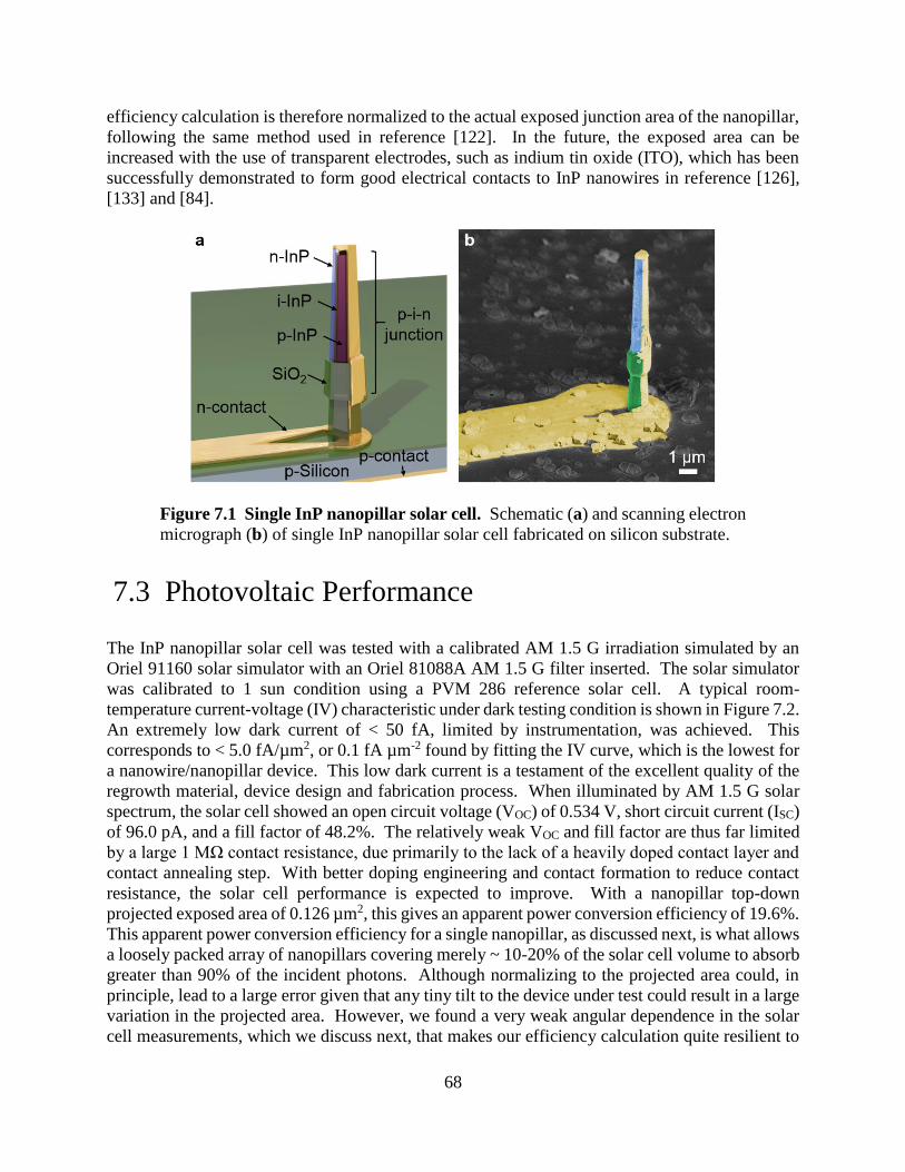
68
efficiency calculation is therefore normalized to the actual exposed junction area of the nanopillar,
following the same method used in reference [122]. In the future, the exposed area can be
increased with the use of transparent electrodes, such as indium tin oxide (ITO), which has been
successfully demonstrated to form good electrical contacts to InP nanowires in reference [126],
[133] and [84].
Figure 7.1 Single InP nanopillar solar cell. Schematic (a) and scanning electron
micrograph (b) of single InP nanopillar solar cell fabricated on silicon substrate.
7.3 Photovoltaic Performance
The InP nanopillar solar cell was tested with a calibrated AM 1.5 G irradiation simulated by an
Oriel 91160 solar simulator with an Oriel 81088A AM 1.5 G filter inserted. The solar simulator
was calibrated to 1 sun condition using a PVM 286 reference solar cell. A typical room-
temperature current-voltage (IV) characteristic under dark testing condition is shown in Figure 7.2.
An extremely low dark current of < 50 fA, limited by instrumentation, was achieved. This
corresponds to < 5.0 fA/µm2, or 0.1 fA µm-2 found by fitting the IV curve, which is the lowest for
a nanowire/nanopillar device. This low dark current is a testament of the excellent quality of the
regrowth material, device design and fabrication process. When illuminated by AM 1.5 G solar
spectrum, the solar cell showed an open circuit voltage (VOC) of 0.534 V, short circuit current (ISC)
of 96.0 pA, and a fill factor of 48.2%. The relatively weak VOC and fill factor are thus far limited
by a large 1 MΩ contact resistance, due primarily to the lack of a heavily doped contact layer and
contact annealing step. With better doping engineering and contact formation to reduce contact
resistance, the solar cell performance is expected to improve. With a nanopillar top-down
projected exposed area of 0.126 µm2, this gives an apparent power conversion efficiency of 19.6%.
This apparent power conversion efficiency for a single nanopillar, as discussed next, is what allows
a loosely packed array of nanopillars covering merely ~ 10-20% of the solar cell volume to absorb
greater than 90% of the incident photons. Although normalizing to the projected area could, in
principle, lead to a large error given that any tiny tilt to the device under test could result in a large
variation in the projected area. However, we found a very weak angular dependence in the solar
cell measurements, which we discuss next, that makes our efficiency calculation quite resilient to

69
error as a 5° deviation of solar incident angle results in merely a 1.1% change in the ISC.
Normalizing ISC to the projected exposed area yields a short circuit current density (JSC) of 76.3
mA/cm2. This is more than a factor of two higher than the JSC of 32.2 mA cm-2 predicted by
Shockley-Queisser limit for a planar solar cell. This more than twice higher JSC is a result of the
nanopillar antenna effect that makes the effective optical capture cross section larger than the
physical cross section of the nanopillar.
Figure 7.2 Single nanopillar solar cell electrical characteristics. a, b, Room-
temperature dark and 1 sun (AM 1.5 G) IV characteristics of a single InP nanopillar
solar cell in linear (a) and log (b) scale. c, VOC as a function of temperature showing
that the VOC can reach 0.7 V at -100°C.
7.4 Temperature Dependence
With a lower operating temperature, the open circuit voltage VOC is expected to improve since
lower operating temperature reduces dark current, while widening the band gap of the material at
the same time. Here we observed VOC increased monotonically at a rate of 1.4 mV/°C when the
device was cooled, and eventually reached 0.7 V at -100°C, as shown in Figure 7.3. This rate of
change for VOC is much faster than k/q because the band gap energy increases at lower temperature.
As for the short circuit current, it drops 0.5 pA every °C because of the widening of the band gap
reduces the amount of photons absorbed. In the end, we observed that the efficiency of the solar
cell peaks at 19.6% at 25°C. This observation is most likely due to the deterioration of the fill
factor as the operating temperature cools.
Dark
1 Sun
Voc
= 0.534 V
Isc
= 96.0 pA
FF = 48.2% Dark
1 Sun
a b
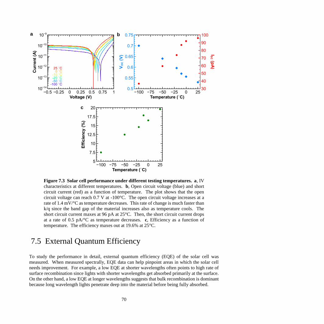
70
Figure 7.3 Solar cell performance under different testing temperatures. a, IV
characteristics at different temperatures. b, Open circuit voltage (blue) and short
circuit current (red) as a function of temperature. The plot shows that the open
circuit voltage can reach 0.7 V at -100°C. The open circuit voltage increases at a
rate of 1.4 mV/°C as temperature decreases. This rate of change is much faster than
k/q since the band gap of the material increases also as temperature cools. The
short circuit current maxes at 96 pA at 25°C. Then, the short circuit current drops
at a rate of 0.5 pA/°C as temperature decreases. c, Efficiency as a function of
temperature. The efficiency maxes out at 19.6% at 25°C.
7.5 External Quantum Efficiency
To study the performance in detail, external quantum efficiency (EQE) of the solar cell was
measured. When measured spectrally, EQE data can help pinpoint areas in which the solar cell
needs improvement. For example, a low EQE at shorter wavelengths often points to high rate of
surface recombination since lights with shorter wavelengths get absorbed primarily at the surface.
On the other hand, a low EQE at longer wavelengths suggests that bulk recombination is dominant
because long wavelength lights penetrate deep into the material before being fully absorbed.
a b
c
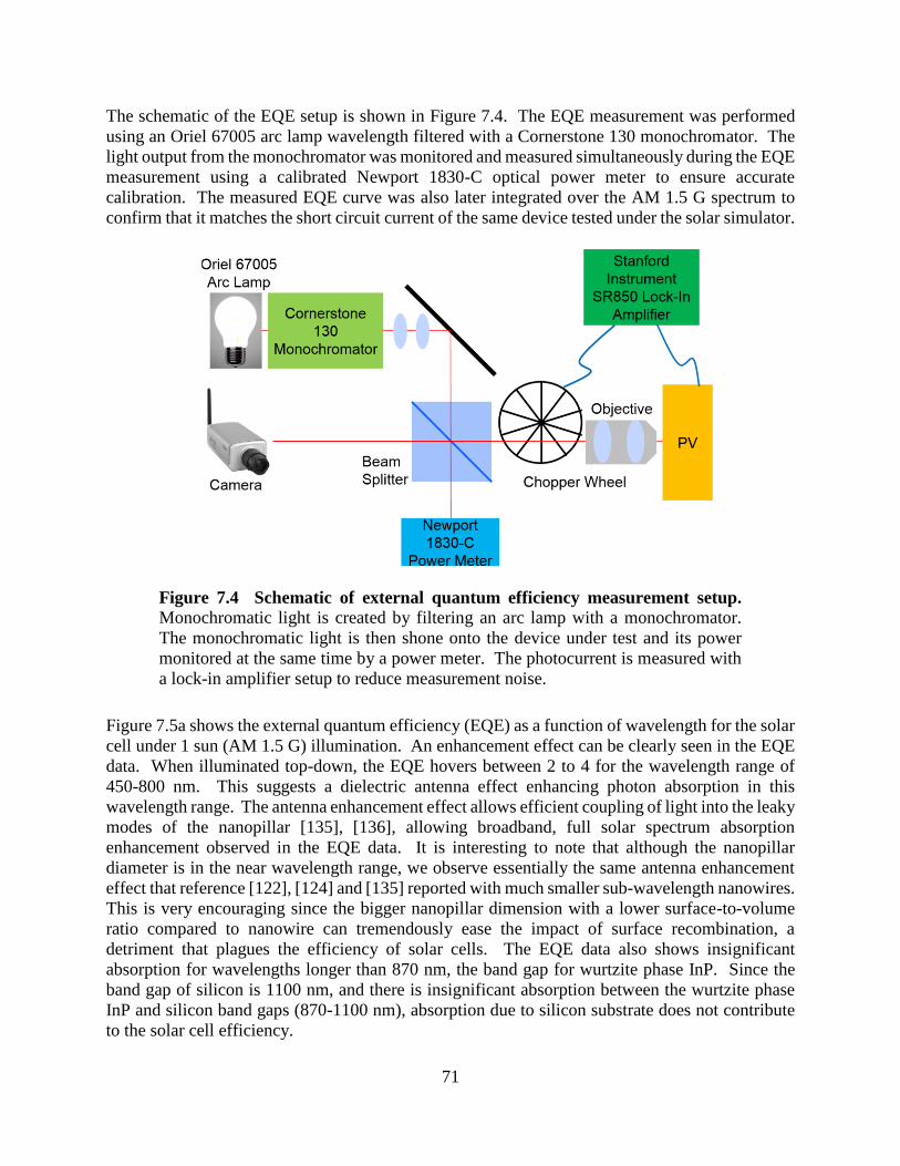
71
The schematic of the EQE setup is shown in Figure 7.4. The EQE measurement was performed
using an Oriel 67005 arc lamp wavelength filtered with a Cornerstone 130 monochromator. The
light output from the monochromator was monitored and measured simultaneously during the EQE
measurement using a calibrated Newport 1830-C optical power meter to ensure accurate
calibration. The measured EQE curve was also later integrated over the AM 1.5 G spectrum to
confirm that it matches the short circuit current of the same device tested under the solar simulator.
Figure 7.4 Schematic of external quantum efficiency measurement setup.
Monochromatic light is created by filtering an arc lamp with a monochromator.
The monochromatic light is then shone onto the device under test and its power
monitored at the same time by a power meter. The photocurrent is measured with
a lock-in amplifier setup to reduce measurement noise.
Figure 7.5a shows the external quantum efficiency (EQE) as a function of wavelength for the solar
cell under 1 sun (AM 1.5 G) illumination. An enhancement effect can be clearly seen in the EQE
data. When illuminated top-down, the EQE hovers between 2 to 4 for the wavelength range of
450-800 nm. This suggests a dielectric antenna effect enhancing photon absorption in this
wavelength range. The antenna enhancement effect allows efficient coupling of light into the leaky
modes of the nanopillar [135], [136], allowing broadband, full solar spectrum absorption
enhancement observed in the EQE data. It is interesting to note that although the nanopillar
diameter is in the near wavelength range, we observe essentially the same antenna enhancement
effect that reference [122], [124] and [135] reported with much smaller sub-wavelength nanowires.
This is very encouraging since the bigger nanopillar dimension with a lower surface-to-volume
ratio compared to nanowire can tremendously ease the impact of surface recombination, a
detriment that plagues the efficiency of solar cells. The EQE data also shows insignificant
absorption for wavelengths longer than 870 nm, the band gap for wurtzite phase InP. Since the
band gap of silicon is 1100 nm, and there is insignificant absorption between the wurtzite phase
InP and silicon band gaps (870-1100 nm), absorption due to silicon substrate does not contribute
to the solar cell efficiency.

72
Figure 7.5 Single nanopillar solar cell external quantum efficiency. EQE of
InP nanopillar solar cell with top-down illumination showing an enhanced EQE of
2-4 for most wavelengths.
The photocurrent map displayed in Figure 7.6, generated by scanning a 2.4 µm wide 660 nm laser
beam across the nanopillar solar cell, also reveals negligible photocurrent contribution from the
silicon substrate. As highlighted by the blue outline in Fig. 4b, the resulting photocurrent spot has
a full-width at half-maximum of 2.3 µm, which is simply the width of the excitation laser beam.
This result further proves that the photocurrent measured indeed comes solely from carriers
generated within the InP nanopillar, as photocurrent was collected only when the laser spot was
shone directly onto the nanopillar solar cell.
Figure 7.6 Photocurrent map of the single InP nanopillar solar cell generated
by scannning a 660 nm laser beam that was focused to a 2.4 µm spot. The blue
trace highlights the half-maximum data in the photocurrent map. The full-width at
half-maximum of the photocurrent spot is 2.3 µm wide, indicating that photocurrent
0 5 10 15 20
15
10
5
20 1.0
0.8
0.6
0.4
0.2
0
X-Displacement (µm)
Y-D
isp
lace
men
t (µ
m)
Photocurrent (a.u.)
X Displacement (m)
Y D
ispl
acem
ent (
m
)
0 5 10 15 200
5
10
15
20
0
0.2
0.4
0.6
0.8
1.0

73
was collected only when the laser spot was directly shone onto the nanopillar solar
cell. Therefore, photogenerated carriers are collected from within the InP
nanopillar only.
7.6 Dielectric Antenna Effect and Angle Insensitivity
As alluded in the previous sections, the single InP nanopillar solar cell receives some kind of
performance enhancement due to dielectric antenna effect. This dielectric antenna effect is evident
in the IV measurements of the solar cell for different illumination angles. The open circuit voltage
and short circuit current both increase with incidence angle as shown in Figure 7.7a and Figure
7.7b, respectively. Open circuit voltage and short circuit current are both expected to increase
since the capture cross-section of the nanopillar solar cell increases with illumination angle. But
the surprising part is the amount of increase. Instead of simply scaling proportionally to the capture
area of the solar cell, the ISC was found to increase by only a factor of 2.9 despite a calculated 33
times increase in solar cell exposed capture area. This rather angle insensitive photovoltaic output
is the result of the dielectric antenna effect enhancing optical absorption for near on-axis
illumination [136], which can be clearly seen in the JSC plot in Figure 7.7b. The tapered sidewalls
of the nanopillar also create a much stronger and tighter focusing effect for near on-axis
illumination compared to non-tapered nanopillars, allowing for much greater absorption
enhancement for near on-axis illumination that would not have otherwise experienced with non-
tapered nanopillars [137]. Thus, the resulting much more pronounced enhancement effect for near
on-axis illumination and the subsequent leveling off of this enhancement effect at higher incident
angles counterbalance nicely for the change in the physical capture cross-section of the nanopillar
solar cell, giving rise to its angle insensitive response. With further optimization on the taper angle
and dimensions of the nanopillar, it is possible to create a nanopillar solar cell that is completely
angle insensitive. Hence, it is clear that the antenna effect not only improves the solar cell
performance but also enables illumination angle insensitive response. This allows solar cells made
with tapered nanopillars to have reliable and steady power output without the need of expensive
solar tracking system to adjust for sun light angle of illumination changes during the day and
throughout seasons.
Figure 7.7 Single nanopillar solar cell angular response. a, Device open circuit
voltage VOC as a function of illumination angle in polar coordinate. The inset shows
b
Figure 6 – Measured angular dependence
Open Circuit Voltage (V)
0.4 0.5
θ
0.6
0.6
0.5
0.4
Short Circuit Current (pA)
10 20 50 100 200 500
Are
a (
µm
2)
0.125
0.25
0.625
2.5
6.25
1.25
a
c
Area
ISC
1 10 100
Short Circuit Current Density (mA cm-2)
2 5 20 50
3.1
1.55
0.62
0.31
0.155
0.062
0.031
Ex
tern
al Q
ua
ntu
m E
ffic
ien
cy
b
Figure 6 – Measured angular dependence
Open Circuit Voltage (V)
0.4 0.5
θ
0.6
0.6
0.5
0.4
Short Circuit Current (pA)
10 20 50 100 200 500
Are
a (
µm
2)
0.125
0.25
0.625
2.5
6.25
1.25
a
c
Area
ISC
1 10 100
Short Circuit Current Density (mA cm-2)
2 5 20 50
3.1
1.55
0.62
0.31
0.155
0.062
0.031
Ex
tern
al Q
uan
tum
Eff
icie
ncy

74
how the illumination angle θ is defined with the respect to the nanopillar. b, Device
short circuit current ISC. Even though the device area increases by a factor of 33
when the illumination angle is changed from 0° to 80°, the short circuit current
increases by only a factor of 3 due to an antenna enhancement effect. c, Normalized
capture area of the solar cell and measured antenna enhancement effect at different
illumination angles. The enhancement effect is greatest near 0°. This compensates
for the reduced capture area of the solar cell. These two counteracting effects give
rise to the angle insensitivity of the device.
Simulation of the solar cell structure with finite-difference time-domain confirms our experimental
results of enhancement due to dielectric antenna. Figure 7.8a shows the simulated ISC as a function
of incident angle, co-plotted against the change in capture area. Again, the simulated ISC changes
much slowly and differently than the capture area of the solar cell. The simulated JSC plot
displayed in Figure 7.8b also confirms the antenna enhancement effect favoring near on-axis
illumination as the source of the insensitive angular response. Although the enhancement effect
for the micron-sized nanopillars is somewhat smaller compared to that of nanowires with deep
sub-wavelength diameter [122], the resulting lower surface-to-volume ratio reduces the impact of
surface recombination, which is especially detrimental to the efficiency of III-V nanowire solar
cells [58], [84]. The antenna enhancement effect also makes the absorption cross-section appear
bigger than the physical capture cross-section, allowing sparsely populated nanopillar array to
absorb almost all of the incident sunlight. The simulation data plotted in Figure 7.8c clearly
supports this claim with two InP nanopillar arrays absorbing 90% of the solar spectrum with
merely 17% of the solar cell volume filled with nanopillars. And with the tapered sidewalls of the
nanopillar creating more leaky resonator modes compared to non-tapered nanopillar [59], light can
be more readily coupled into the nanopillar body [137]. Thus, compared to nanopillar arrays with
vertical sidewalls (red trace in Figure 7.8c), tapered nanopillar arrays (blue trace in Figure 7.8c)
display higher light absorption at 95% (versus 90% by the non-tapered nanopillar arrays), even
when both arrays have the same 17% volume fill ratio. Therefore, solar cell efficiency can be
further improved with tapered nanopillars.
Figure 7.8 Simulated angular response of a single nanopillar solar cell and
simulated absorption from a nanopillar array. a, Simulated short circuit current
ISC (red) also shows angle insensitive response that scales very differently from the
change in the capture area of the solar cell (blue). b, Simulated short circuit current
density JSC confirms the directional antenna enhancement effect compensating for
Short Circuit Current (nA)
0.05 0.1 0.25 1 2.5 5
Are
a (
µm
2)
1
10
0.1
0.2
0.5
2
5
0.5
θ
a b
c
Area
ISC
Ex
tern
al Q
ua
ntu
m E
ffic
ien
cy
0.132 160
0.2
0.5
1
2
5
10
Short Circuit Current Density (mA cm-2)64 320166.43.2
Short Circuit Current (nA)
0.05 0.1 0.25 1 2.5 5
Are
a (
µm
2)
1
10
0.1
0.2
0.5
2
5
0.5
θ
a b
c
Area
ISC
Ex
tern
al Q
ua
ntu
m E
ffic
ien
cy
0.132 160
0.2
0.5
1
2
5
10
Short Circuit Current Density (mA cm-2)64 320166.43.2
b
Figure 6 – Measured angular dependence
Open Circuit Voltage (V)
0.4 0.5
θ
0.6
0.6
0.5
0.4
Short Circuit Current (pA)
10 20 50 100 200 500
Are
a (
µm
2)
0.125
0.25
0.625
2.5
6.25
1.25
a
c
Area
ISC
1 10 100
Short Circuit Current Density (mA cm-2)
2 5 20 50
3.1
1.55
0.62
0.31
0.155
0.062
0.031
Ex
tern
al Q
ua
ntu
m E
ffic
ien
cy
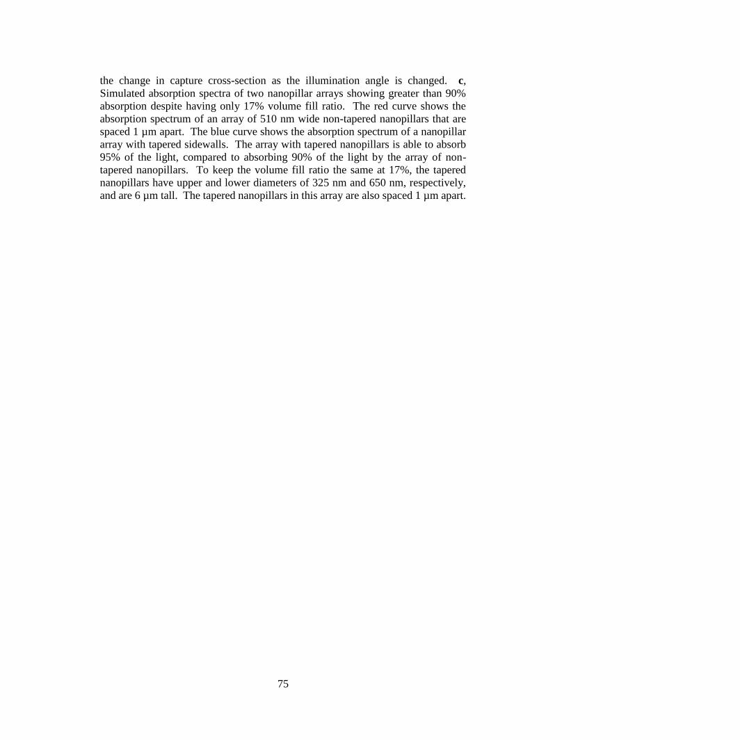
75
the change in capture cross-section as the illumination angle is changed. c,
Simulated absorption spectra of two nanopillar arrays showing greater than 90%
absorption despite having only 17% volume fill ratio. The red curve shows the
absorption spectrum of an array of 510 nm wide non-tapered nanopillars that are
spaced 1 µm apart. The blue curve shows the absorption spectrum of a nanopillar
array with tapered sidewalls. The array with tapered nanopillars is able to absorb
95% of the light, compared to absorbing 90% of the light by the array of non-
tapered nanopillars. To keep the volume fill ratio the same at 17%, the tapered
nanopillars have upper and lower diameters of 325 nm and 650 nm, respectively,
and are 6 µm tall. The tapered nanopillars in this array are also spaced 1 µm apart.

76
Chapter 8
On-Chip Optical Data Link
Light emitters and detectors discussed in previous chapters are paramount to realizing chip scale
photonic integrated circuits, so is finding a way to interconnect them. Already, massively
integrating photonic components and interconnecting them has given photonic integrated circuits
tremendous amount of new capabilities that no single component can replicate [3], [138]. Here,
we present an interconnect scheme using waveguides fabricated top-down, and demonstrate a
complete on-chip optical data link built entirely out of nanopillars. And with the radically reduced
footprints of nanopillars compared to conventional optical devices, optical components can be
packed much more densely to extend the Moore’s Law equivalent in photonics [139]. This
demonstration will no doubt lay the pathway towards a future generation of large scale, densely
populated photonic integrated circuits built alongside silicon electronics.
8.1 Interconnecting Nanopillars with Waveguides
Figure 8.1 Nanopillar optical link built on silicon. a, Schematic of a nanopillar
optical link. b, Scanning electron micrograph of a fabricated optical link. The inset
shows the microscope images of a nanopillar light emitting diode with metal coated
only on one side, and its crescent shape light emission.
Waveguides are essential to photonic systems. Although silicon waveguide has been developed
[140], integration scheme with nanopillar devices has yet to be realized. An alternative to silicon
waveguide that is compatible to silicon photonics, yet easy to integrate with nanopillar devices is
polymer waveguide. When well designed, these polymer waveguides can support single optical
mode with low loss [141]. Using negative tone electron beam photoresist, we fabricated polymer
a
10 µm
b
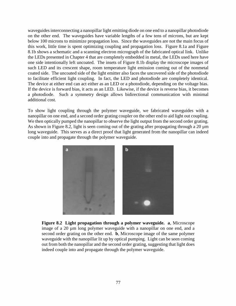
77
waveguides interconnecting a nanopillar light emitting diode on one end to a nanopillar photodiode
on the other end. The waveguides have variable lengths of a few tens of microns, but are kept
below 100 microns to minimize propagation loss. Since the waveguides are not the main focus of
this work, little time is spent optimizing coupling and propagation loss. Figure 8.1a and Figure
8.1b shows a schematic and a scanning electron micrograph of the fabricated optical link. Unlike
the LEDs presented in Chapter 4 that are completely embedded in metal, the LEDs used here have
one side intentionally left uncoated. The insets of Figure 8.1b display the microscope images of
such LED and its crescent shape, room temperature light emission coming out of the nonmetal
coated side. The uncoated side of the light emitter also faces the uncovered side of the photodiode
to facilitate efficient light coupling. In fact, the LED and photodiode are completely identical.
The device at either end can act either as an LED or a photodiode, depending on the voltage bias.
If the device is forward bias, it acts as an LED. Likewise, if the device is reverse bias, it becomes
a photodiode. Such a symmetry design allows bidirectional communication with minimal
additional cost.
To show light coupling through the polymer waveguide, we fabricated waveguides with a
nanopillar on one end, and a second order grating coupler on the other end to aid light out coupling.
We then optically pumped the nanopillar to observe the light output from the second order grating.
As shown in Figure 8.2, light is seen coming out of the grating after propagating through a 20 µm
long waveguide. This serves as a direct proof that light generated from the nanopillar can indeed
couple into and propagate through the polymer waveguide.
Figure 8.2 Light propagation through a polymer waveguide. a, Microscope
image of a 20 µm long polymer waveguide with a nanopillar on one end, and a
second order grating on the other end. b, Microscope image of the same polymer
waveguide with the nanopillar lit up by optical pumping. Light can be seen coming
out from both the nanopillar and the second order grating, suggesting that light does
indeed couple into and propagate through the polymer waveguide.
a b

78
8.2 Optical Link Operation
The optical links were tested under both direct current (DC) and alternating current (AC)
conditions. When the LED was pumped with 400 µA of current, a shift in IV behavior, which
indicates photocurrent, can be clearly seen from the photodiode IVs shown in Figure 8.3a. An on-
off signal of approximately 300 pA, which is displayed at Figure 8.3b, can also be seen at the
photodiode when the LED is turned on and off. Although the detected signal is nice and clear, it
is a far cry from the input current level. However, little work went into the design and optimization
of the waveguide for this proof-of-concept. Therefore, coupling and propagation loss are likely
extremely high, which leads to the high amount of signal loss observed.
Figure 8.3 Optical link data transmission demonstration. a, IV curves of the
photodiode when the LED is switched on (red) and off (blue). b, Photocurrent
detected by the photodiode when the LED is turned on and off. c, Signal received
by the photodiode when a 100 Hz signal is sent by the LED.
Practical data links do not only communicate with DC signals, but also with AC signals that require
constant modulation of optical pulses. As such, we tested the optical links with AC signals. Figure
8.3b shows the clear signal received by the photodiode when a 100 Hz sinusoidal AC signal is sent
by the LED, providing direct evidence that the optical links are capable of transmitting data. While
100 Hz is modest at best, this is a first of a kind demonstration of an optical data link built entirely
out of nanostructures on silicon. With nanostructures, the combined footprints of the light emitter
and detector total to less than 10 µm2. This represents an order of magnitude savings in chip area
compared to the well over 200 µm2 space required with conventional light emitter and detector
technologies [142], [143]. Such impressive space savings open the door to a new generation of
densely packed, on-chip optical data links. Although only 100 Hz transmission is shown, higher
data rate should also be possible, as both the LED and photodiode can operate at speeds in the GHz
range. It is only because equipment limitations limited our ability to show higher speed operation.
0 50 100 150
-0.4
-0.2
0.0
Curr
en
t (n
A)
Time (s)
0 10 20 30 40
0
2
4
Sig
na
l (a
.u.)
Time (ms)
a
b
c LED On
LED Off

79
At speeds beyond 1 kHz, radio frequency coupling noise between adjacent probes used for biasing
drowns out the received photocurrent signal, which makes data recovery impossible.
80
Chapter 9
Conclusion
Mixing and matching dissimilar items to create something more useful is undeniably a very
powerful concept. Humans have applied this concept throughout history to bring us many of the
life changing inventions that we enjoy today. And with today’s largely disjoint electronic and
photonic integrated circuits, it would only be sensible to try to integrate the two to create a new,
more capable combined photonic-electronic platform.
This dissertation showed the pathway and viability towards such a combined photonic-electronic
platform with III-V nanopillars. We used a newly discovered growth technique to synthesize
virtually single crystalline (In)GaAs and InP nanopillars on silicon substrates at CMOS compatible
temperatures. These nanopillars show excellent optical qualities, allowing them to become on-
chip, optically pump nano lasers. The growth of the nanopillar is also highly controllable. For
example, the size and shape of these nanopillars can be controlled by changing the growth time
and growth condition. The growth location of the nanopillar, though preliminary, can also be
controlled with high precision using a silicon dioxide mask to define nucleation sites.
Having good optical material on silicon alone is not enough to prove success. So we worked to
demonstrate a full array of electrically controlled photonic devices built using nanopillars grown
on silcon. We first demonstrated the operation of high speed light emitting diodes (LEDs). When
put into a metal cavity, the LED emitted stimulated emission at 1.1 µm wavelength. The LED was
also capable of operating at ~ 2.5 GHz speed. With further optimization on the cavity design,
material synthesis and processing techniques, we expect the nano LED can be made into a high
speed nano laser.
We also showed nanopillars as efficient detectors as well. We demonstrated avalanche
photodiodes (APDs) and bipolar junction phototransistor (photo-BJT) built on silicon substrates
using nanopillars. Thanks to the unique core-shell junction, the APD was able to reach a gain of
100 at a low bias voltage of only 1 V. And to enable even tighter integration and lower energy
consumption, we integrated a sensitive photodiode into a receiver circuit to create a photo-BJT
with 4 A/W responsivity. These two sensitive photo-detector devices can certainly help pave the
way to low energy applications, such as optical interconnects.
Nanopillars are also great on-chip energy scavenger devices. We demonstrated a record breaking
single InP nanopillar solar cell grown on silicon substrate with 19.6% power conversion efficiency.
The solar cell displayed absorption enhancement factor of 2~4 when illuminated top-down due to
the presence of dielectric antenna effect. As a result of the enhancement and antenna effect, the
solar cell output exhibit an interesting angle insensitive characteristic, making it well-suited for
low cost or no tracking system to adjust for sun ray directionality during the day and seasonal

81
shifts. As a high efficiency, angle insensitive solar cell grown on low cost silicon substrate, InP
nanopillar solar cell can potentially be a game changer in making solar energy more affordable
and widely deployed, and can possible be used as an on-chip power generator to power the
electronic circuitries.
The nanopillar based light emitting diodes, avalanche photodiodes and phototransistors discuss
represented components paramount to the realization of full photonics integration with electronics.
But we wanted to demonstrate that they can actually work together as a photonic integrated circuit.
As a demonstration, we connected a LED and a photodiode to create a fully functional on-chip
optical data link.
With all these multifaceted photonic device demonstrations on silicon, III-V nanopillars truly
establish themselves feasible in bridging the gap between photonics and electronics. Not only are
nanopillars highly capable, the small footprints of nanopillars also dramatically reduce the amount
of real estate needed when compared to conventional photonic devices. So perhaps with further
development, nanopillars will one day become the enabler in the building of next generation, ultra-
dense photonic integrated circuits living alongside silicon electronic integrated circuits. And when
paired with the capability, scalability and flexibility of CMOS, these photonic capable integrated
circuits will undeniably bring unparalleled performance and opportunities, many of which are
likely yet to be discovered.

82
References
[1] G. E. Moore, “Cramming more components onto integrated circuits,” Electronics, vol. 38,
no. 8, pp. 114–117, 1965.
[2] D. A. B. Miller, “Device Requirements for Optical Interconnects to Silicon Chips,” Proc.
IEEE, vol. 97, no. 7, pp. 1166–1185, Jul. 2009.
[3] R. Nagarajan, C. H. Joyner, R. P. Schneider, J. S. Bostak, T. Butrie, A. G. Dentai, V. G.
Dominic, P. W. Evans, M. Kato, M. Kauffman, D. J. H. Lambert, S. K. Mathis, A.
Mathur, R. H. Miles, M. L. Mitchell, M. J. Missey, S. Murthy, A. C. Nilsson, F. H. Peters,
S. C. Pennypacker, J. L. Pleumeekers, R. A. Salvatore, R. K. Schlenker, R. B. Taylor, M.
F. Van Leeuwen, J. Webjorn, M. Ziari, D. Perkins, J. Singh, S. G. Grubb, M. S. Reffle, D.
G. Mehuys, F. A. Kish, and D. F. Welch, “Large-scale photonic integrated circuits,” IEEE
J. Sel. Top. Quantum Electron., vol. 11, no. 1, pp. 50–65, Jan. 2005.
[4] J. Sun, E. Timurdogan, A. Yaacobi, E. S. Hosseini, and M. R. Watts, “Large-scale
nanophotonic phased array.,” Nature, vol. 493, no. 7431, pp. 195–199, Jan. 2013.
[5] H. Schmidt and A. R. Hawkins, “The photonic integration of non-solid media using
optofluidics,” Nat. Photonics, vol. 5, no. 10, pp. 598–604, Aug. 2011.
[6] R. M. Lum, J. K. Klingert, R. B. Bylsma, a. M. Glass, a. T. Macrander, T. D. Harris, and
M. G. Lamont, “Effects of misfit dislocations and thermally induced strain on the film
properties of heteroepitaxial GaAs on Si,” J. Appl. Phys., vol. 64, no. 12, p. 6727, 1988.
[7] J. W. Matthews and A. E. Blakeslee, “Defects in epitaxial multilayers,” J. Cryst. Growth,
vol. 27, pp. 118–125, Dec. 1974.
[8] S. F. Fang, K. Adomi, S. Iyer, H. Morkoc, H. Zabel, C. Choi, and N. Otsuka, “Gallium
arsenide and other compound semiconductors on silicon,” J. Appl. Phys., vol. 68, no. 7, p.
R31, 1990.
[9] D. K. Biegelsen, F. a. Ponce, a. J. Smith, and J. C. Tramontana, “Initial stages of epitaxial
growth of GaAs on (100) silicon,” J. Appl. Phys., vol. 61, no. 5, p. 1856, 1987.
[10] A. Krost, R. F. Schnabel, F. Heinrichsdorff, U. Rossow, D. Bimberg, and H. Cerva,
“Defect reduction in GaAs and InP grown on planar Si(111) and on patterned Si(001)
substrates,” J. Cryst. Growth, vol. 145, no. 1–4, pp. 314–320, Dec. 1994.
[11] G. Wang, M. R. Leys, R. Loo, O. Richard, H. Bender, N. Waldron, G. Brammertz, J.
Dekoster, W. Wang, M. Seefeldt, M. Caymax, and M. M. Heyns, “Selective area growth
of high quality InP on Si (001) substrates,” Appl. Phys. Lett., vol. 97, no. 12, p. 121913,
2010.

83
[12] M. E. Groenert, C. W. Leitz, A. J. Pitera, V. Yang, H. Lee, R. J. Ram, and E. a. Fitzgerald,
“Monolithic integration of room-temperature cw GaAs/AlGaAs lasers on Si substrates via
relaxed graded GeSi buffer layers,” J. Appl. Phys., vol. 93, no. 1, p. 362, 2003.
[13] G. S. Matijasevic, C. Y. Wang, and C. C. Lee, “Void free bonding of large silicon dice
using gold-tin alloys,” IEEE Trans. Components, Hybrids, Manuf. Technol., vol. 13, no. 4,
pp. 1128–1134, 1990.
[14] A. Fan, “Copper Wafer Bonding,” Electrochem. Solid-State Lett., vol. 2, no. 10, p. 534,
1999.
[15] M. a. Schmidt, “Wafer-to-wafer bonding for microstructure formation,” Proc. IEEE, vol.
86, no. 8, pp. 1575–1585, 1998.
[16] C. H. Tsau, S. M. Spearing, and M. A. Schmidt, “Fabrication of wafer-level
thermocompression bonds,” J. Microelectromechanical Syst., vol. 11, no. 6, pp. 641–647,
Dec. 2002.
[17] K. Goossen and J. Walker, “GaAs MQW modulators integrated with silicon CMOS,”
IEEE Photonics Technol. Lett., vol. 7, no. 4, pp. 360–362, 1995.
[18] K. Tanabe, K. Watanabe, and Y. Arakawa, “III-V/Si hybrid photonic devices by direct
fusion bonding.,” Sci. Rep., vol. 2, p. 349, Jan. 2012.
[19] K. Tanabe, D. Guimard, D. Bordel, S. Iwamoto, and Y. Arakawa, “InAs / GaAs quantum
dot lasers on Si substrates by metal-mediated wafer bonding and layer transfer,” Opt.
Express, vol. 18, no. 10, pp. 10604–10608, 2010.
[20] T. Okumura, T. Maruyama, M. Kanemaru, S. Sakamoto, and S. Arai, “Single-Mode
Operation of GaInAsP/InP-Membrane Distributed Feedback Lasers Bonded on Silicon-
on-Insulator Substrate with Rib-Waveguide Structure,” Jpn. J. Appl. Phys., vol. 46, no.
No. 48, pp. L1206–L1208, Dec. 2007.
[21] T. Maruyama, T. Okumura, S. Sakamoto, K. Miura, Y. Nishimoto, and S. Arai,
“GaInAsP/InP membrane BH-DFB lasers directly bonded on SOI substrate.,” Opt.
Express, vol. 14, no. 18, pp. 8184–8, Sep. 2006.
[22] K. Matsumoto, X. Zhang, Y. Kanaya, and K. Shimomura, “Selective MOVPE growth of
GaInAs/InP MQW on directly-bonded InP/Si substrate,” Phys. Status Solidi, vol. 10, no.
11, pp. 1357–1360, Nov. 2013.
[23] A. W. Fang, H. Park, O. Cohen, R. Jones, M. J. Paniccia, and J. E. Bowers, “Electrically
pumped hybrid AlGaInAs-silicon evanescent laser.,” Opt. Express, vol. 14, no. 20, pp.
9203–9210, Oct. 2006.
84
[24] C. Camperi-Ginestet, Y. W. Kim, N. M. Jokerst, M. G. Allen, and M. a. Brooke, “Vertical
electrical interconnection of compound semiconductor thin-film devices to underlying
silicon circuitry,” IEEE Photonics Technol. Lett., vol. 4, no. 9, pp. 1003–1006, Sep. 1992.
[25] J. Nah, H. Fang, C. Wang, K. Takei, M. H. Lee, E. Plis, S. Krishna, and A. Javey, “III-V
complementary metal-oxide-semiconductor electronics on silicon substrates.,” Nano Lett.,
vol. 12, no. 7, pp. 3592–3595, Jul. 2012.
[26] H. Yang, D. Zhao, S. Chuwongin, J. Seo, W. Yang, Y. Shuai, J. Berggren, M. Hammar, Z.
Ma, and W. Zhou, “Transfer-printed stacked nanomembrane lasers on silicon,” Nat.
Photonics, vol. 6, no. 9, pp. 617–622, Jul. 2012.
[27] B. Kunert, J. Koch, T. Torunski, K. Volz, and W. Stolz, “MOVPE growth experiments of
the novel (GaIn)(NP)/GaP material system,” J. Cryst. Growth, vol. 272, no. 1–4, pp. 753–
759, Dec. 2004.
[28] B. Kunert, K. Volz, J. Koch, and W. Stolz, “Direct-band-gap Ga(NAsP)-material system
pseudomorphically grown on GaP substrate,” Appl. Phys. Lett., vol. 88, no. 18, p. 182108,
2006.
[29] B. Kunert, K. Volz, and W. Stolz, Dilute III-V Nitride Semiconductors and Material
Systems, vol. 105. Berlin, Heidelberg: Springer Berlin Heidelberg, 2008.
[30] S. Liebich, M. Zimprich, a. Beyer, C. Lange, D. J. Franzbach, S. Chatterjee, N. Hossain,
S. J. Sweeney, K. Volz, B. Kunert, and W. Stolz, “Laser operation of Ga(NAsP) lattice-
matched to (001) silicon substrate,” Appl. Phys. Lett., vol. 99, no. 7, p. 071109, 2011.
[31] H. Takeuchi, A. Wung, X. Sun, R. T. Howe, and T.-J. King, “Thermal Budget Limits of
Quarter-Micrometer Foundry CMOS for Post-Processing MEMS Devices,” IEEE Trans.
Electron Devices, vol. 52, no. 9, pp. 2081–2086, Sep. 2005.
[32] Y. Liu, M. D. Deal, and J. D. Plummer, “Rapid Melt Growth of Germanium Crystals with
Self-Aligned Microcrucibles on Si Substrates,” J. Electrochem. Soc., vol. 152, no. 8, p.
G688, 2005.
[33] M. Miyao, K. Toko, T. Tanaka, and T. Sadoh, “High-quality single-crystal Ge stripes on
quartz substrate by rapid-melting-growth,” Appl. Phys. Lett., vol. 95, no. 2, p. 022115,
2009.
[34] R. E. Camacho-Aguilera, Y. Cai, N. Patel, J. T. Bessette, M. Romagnoli, L. C. Kimerling,
and J. Michel, “An electrically pumped germanium laser.,” Opt. Express, vol. 20, no. 10,
pp. 11316–11320, May 2012.
[35] J. R. Jain, A. Hryciw, T. M. Baer, D. A. B. Miller, M. L. Brongersma, and R. T. Howe, “A
micromachining-based technology for enhancing germanium light emission via tensile
strain,” Nat. Photonics, vol. 6, no. 6, pp. 398–405, May 2012.
85
[36] J. R. Sánchez-Pérez, C. Boztug, F. Chen, F. F. Sudradjat, D. M. Paskiewicz, R. B.
Jacobson, M. G. Lagally, and R. Paiella, “Direct-bandgap light-emitting germanium in
tensilely strained nanomembranes.,” Proc. Natl. Acad. Sci. U. S. A., vol. 108, no. 47, pp.
18893–18898, Nov. 2011.
[37] X. Sun, J. Liu, L. C. Kimerling, and J. Michel, “Room-temperature direct bandgap
electroluminesence from Ge-on-Si light-emitting diodes.,” Opt. Lett., vol. 34, no. 8, pp.
1198–1200, Apr. 2009.
[38] J. Liu, X. Sun, L. C. Kimerling, and J. Michel, “Direct-gap optical gain of Ge on Si at
room temperature.,” Opt. Lett., vol. 34, no. 11, pp. 1738–1740, Jun. 2009.
[39] J. Liu, X. Sun, Y. Bai, K. E. Lee, E. A. Fitzgerald, L. C. Kimerling, and J. Michel,
“Efficient above-band-gap light emission in germanium,” Chinese Opt. Lett., vol. 7, no. 4,
pp. 271–273, 2009.
[40] T. Wang, H. Liu, A. Lee, F. Pozzi, and A. Seeds, “1.3-μm InAs/GaAs quantum-dot lasers
monolithically grown on Si substrates,” Opt. Express, vol. 19, no. 12, pp. 11381–11386,
2011.
[41] A. Lee, Q. Jiang, M. Tang, A. Seeds, and H. Liu, “Continuous-wave InAs/GaAs quantum-
dot laser diodes monolithically grown on Si substrate with low threshold current
densities.,” Opt. Express, vol. 20, no. 20, pp. 22181–7, Sep. 2012.
[42] L. C. Chuang, M. Moewe, S. Crankshaw, and C. Chang-Hasnain, “Optical properties of
InP nanowires on Si substrates with varied synthesis parameters,” Appl. Phys. Lett., vol.
92, no. 1, p. 013121, 2008.
[43] N. P. Dasgupta, J. Sun, C. Liu, S. Brittman, S. C. Andrews, J. Lim, H. Gao, R. Yan, and P.
Yang, “25th anniversary article: semiconductor nanowires - synthesis, characterization,
and applications.,” Adv. Mater., vol. 26, no. 14, pp. 2137–2184, Apr. 2014.
[44] R. S. Wagner and W. C. Ellis, “Vapor-Liquid-Solid Mechanism of Single Crystal
Growth,” Appl. Phys. Lett., vol. 4, no. 5, p. 89, 1964.
[45] S. Hertenberger, D. Rudolph, M. Bichler, J. J. Finley, G. Abstreiter, and G. Koblmuller,
“Growth kinetics in position-controlled and catalyst-free InAs nanowire arrays on Si(111)
grown by selective area molecular beam epitaxy,” J. Appl. Phys., vol. 108, no. 11, p.
114316, 2010.
[46] V. T. Renard, M. Jublot, P. Gergaud, P. Cherns, D. Rouchon, A. Chabli, and V.
Jousseaume, “Catalyst preparation for CMOS-compatible silicon nanowire synthesis.,”
Nat. Nanotechnol., vol. 4, no. 10, pp. 654–657, Oct. 2009.

86
[47] L. C. Chuang, M. Moewe, C. Chase, N. P. Kobayashi, C. Chang-Hasnain, and S.
Crankshaw, “Critical diameter for III-V nanowires grown on lattice-mismatched
substrates,” Appl. Phys. Lett., vol. 90, no. 4, p. 043115, 2007.
[48] L. A. Coldren, S. W. Corzine, and M. L. Mashanovitch, Diode Lasers and Photonic
Integrated Circuits, 2nd ed. New York, NY: Wiley, 2012, p. 744.
[49] M. Moewe, L. C. Chuang, S. Crankshaw, K. W. Ng, and C. Chang-Hasnain, “Core-shell
InGaAs/GaAs quantum well nanoneedles grown on silicon with silicon-transparent
emission.,” Opt. Express, vol. 17, no. 10, pp. 7831–7836, May 2009.
[50] M. Moewe, L. C. Chuang, S. Crankshaw, C. Chase, and C. Chang-Hasnain, “Atomically
sharp catalyst-free wurtzite GaAs∕AlGaAs nanoneedles grown on silicon,” Appl. Phys.
Lett., vol. 93, no. 2, p. 023116, 2008.
[51] F. Ren, K. Wei Ng, K. Li, H. Sun, and C. J. Chang-Hasnain, “High-quality InP
nanoneedles grown on silicon,” Appl. Phys. Lett., vol. 102, no. 1, p. 012115, 2013.
[52] K. W. Ng, W. S. Ko, T.-T. D. Tran, R. Chen, M. V Nazarenko, F. Lu, V. G. Dubrovskii,
M. Kamp, A. Forchel, and C. J. Chang-Hasnain, “Unconventional growth mechanism for
monolithic integration of III-V on silicon.,” ACS Nano, vol. 7, no. 1, pp. 100–107, Jan.
2013.
[53] K. W. Ng, T.-T. D. Tran, W. S. Ko, R. Chen, F. Lu, and C. J. Chang-Hasnain, “Single
crystalline InGaAs nanopillar grown on polysilicon with dimensions beyond the substrate
grain size limit.,” Nano Lett., vol. 13, no. 12, pp. 5931–5937, Dec. 2013.
[54] F. Lu, T.-T. D. Tran, W. S. Ko, K. W. Ng, R. Chen, and C. Chang-Hasnain, “Nanolasers
grown on silicon-based MOSFETs.,” Opt. Express, vol. 20, no. 11, pp. 12171–12176,
May 2012.
[55] V. G. Dubrovskii, M. V. Nazarenko, L. C. Chuang, W. S. Ko, K. W. Ng, and C. Chang-
Hasnain, “Growth kinetics of GaAs nanoneedles on silicon and sapphire substrates,” Appl.
Phys. Lett., vol. 98, no. 15, p. 153113, 2011.
[56] M. Moewe, L. C. Chuang, V. G. Dubrovskii, and C. Chang-Hasnain, “Growth
mechanisms and crystallographic structure of InP nanowires on lattice-mismatched
substrates,” J. Appl. Phys., vol. 104, no. 4, p. 044313, 2008.
[57] J. V Holm, H. I. Jørgensen, P. Krogstrup, J. Nygård, H. Liu, and M. Aagesen, “Surface-
passivated GaAsP single-nanowire solar cells exceeding 10% efficiency grown on
silicon.,” Nat. Commun., vol. 4, p. 1498, Jan. 2013.
[58] G. Mariani, A. C. Scofield, C.-H. Hung, and D. L. Huffaker, “GaAs nanopillar-array solar
cells employing in situ surface passivation.,” Nat. Commun., vol. 4, p. 1497, Jan. 2013.
87
[59] R. Chen, T.-T. D. Tran, K. W. Ng, W. S. Ko, L. C. Chuang, F. G. Sedgwick, and C.
Chang-Hasnain, “Nanolasers grown on silicon,” Nat. Photonics, vol. 5, no. 3, pp. 170–
175, 2011.
[60] L. M. Smith, H. E. Jackson, J. M. Yarrison-Rice, and C. Jagadish, “Insights into single
semiconductor nanowire heterostructures using time-resolved photoluminescence,”
Semicond. Sci. Technol., vol. 25, no. 2, p. 024010, Feb. 2010.
[61] H. Goto, K. Nosaki, K. Tomioka, S. Hara, K. Hiruma, J. Motohisa, and T. Fukui, “Growth
of Core–Shell InP Nanowires for Photovoltaic Application by Selective-Area Metal
Organic Vapor Phase Epitaxy,” Appl. Phys. Express, vol. 2, p. 035004, Feb. 2009.
[62] P. Mohan, J. Motohisa, and T. Fukui, “Fabrication of InP∕InAs∕InP core-multishell
heterostructure nanowires by selective area metalorganic vapor phase epitaxy,” Appl.
Phys. Lett., vol. 88, no. 13, p. 133105, 2006.
[63] J. Motohisa, J. Noborisaka, J. Takeda, M. Inari, and T. Fukui, “Catalyst-free selective-area
MOVPE of semiconductor nanowires on (111)B oriented substrates,” J. Cryst. Growth,
vol. 272, no. 1–4, pp. 180–185, Dec. 2004.
[64] J. Noborisaka, J. Motohisa, and T. Fukui, “Catalyst-free growth of GaAs nanowires by
selective-area metalorganic vapor-phase epitaxy,” Appl. Phys. Lett., vol. 86, no. 21, p.
213102, 2005.
[65] H. Paetzelt, V. Gottschalch, J. Bauer, G. Benndorf, and G. Wagner, “Selective-area
growth of GaAs and InAs nanowires—homo- and heteroepitaxy using templates,” J.
Cryst. Growth, vol. 310, no. 23, pp. 5093–5097, Nov. 2008.
[66] J. N. Shapiro, a. Lin, P. S. Wong, a. C. Scofield, C. Tu, P. N. Senanayake, G. Mariani, B.
L. Liang, and D. L. Huffaker, “InGaAs heterostructure formation in catalyst-free GaAs
nanopillars by selective-area metal-organic vapor phase epitaxy,” Appl. Phys. Lett., vol.
97, no. 24, p. 243102, 2010.
[67] K. Tomioka, P. Mohan, J. Noborisaka, S. Hara, J. Motohisa, and T. Fukui, “Growth of
highly uniform InAs nanowire arrays by selective-area MOVPE,” J. Cryst. Growth, vol.
298, pp. 644–647, Jan. 2007.
[68] H. J. Fan, P. Werner, and M. Zacharias, “Semiconductor nanowires: from self-
organization to patterned growth.,” Small, vol. 2, no. 6, pp. 700–717, Jun. 2006.
[69] Z. H. Wu, X. Y. Mei, D. Kim, M. Blumin, and H. E. Ruda, “Growth of Au-catalyzed
ordered GaAs nanowire arrays by molecular-beam epitaxy,” Appl. Phys. Lett., vol. 81, no.
27, p. 5177, 2002.
88
[70] T. Mårtensson, M. Borgström, W. Seifert, B. J. Ohlsson, and L. Samuelson, “Fabrication
of individually seeded nanowire arrays by vapour–liquid–solid growth,” Nanotechnology,
vol. 14, no. 12, pp. 1255–1258, Dec. 2003.
[71] T. Mårtensson, P. Carlberg, M. Borgström, L. Montelius, W. Seifert, and L. Samuelson,
“Nanowire Arrays Defined by Nanoimprint Lithography,” Nano Lett., vol. 4, no. 4, pp.
699–702, Apr. 2004.
[72] Y. Kim, H. J. Joyce, Q. Gao, H. H. Tan, C. Jagadish, M. Paladugu, J. Zou, and A. a
Suvorova, “Influence of nanowire density on the shape and optical properties of ternary
InGaAs nanowires.,” Nano Lett., vol. 6, no. 4, pp. 599–604, Apr. 2006.
[73] X. Duan, Y. Huang, R. Agarwal, and C. Lieber, “Single-nanowire electrically driven
lasers,” Nature, vol. 421, no. 6920, pp. 241–245, 2003.
[74] M. T. Hill, Y.-S. Oei, B. Smalbrugge, Y. Zhu, T. de Vries, P. J. van Veldhoven, F. W. M.
van Otten, T. J. Eijkemans, J. P. Turkiewicz, H. de Waardt, E. J. Geluk, S.-H. Kwon, Y.-
H. Lee, R. Nötzel, and M. K. Smit, “Lasing in metallic-coated nanocavities,” Nat.
Photonics, vol. 1, no. 10, pp. 589–594, Sep. 2007.
[75] M. T. Hill, M. Marell, E. S. P. Leong, B. Smalbrugge, Y. Zhu, M. Sun, P. J. van
Veldhoven, E. J. Geluk, F. Karouta, Y.-S. Oei, R. Nötzel, C.-Z. Ning, and M. K. Smit,
“Lasing in metal-insulator-metal sub-wavelength plasmonic waveguides.,” Opt. Express,
vol. 17, no. 13, pp. 11107–11112, Jun. 2009.
[76] K. Ding, M. Hill, Z. Liu, and L. Yin, “Record performance of a CW metallic
subwavelength-cavity laser at room temperature,” in CLEO, 2012, vol. 15, no. 1, p.
CTh4M.3.
[77] K. Ding, Z. C. Liu, L. J. Yin, M. T. Hill, M. J. H. Marell, P. J. van Veldhoven, R. Nöetzel,
and C. Z. Ning, “Room-temperature continuous wave lasing in deep-subwavelength
metallic cavities under electrical injection,” Phys. Rev. B, vol. 85, no. 4, p. 041301, Jan.
2012.
[78] J. H. Lee, M. Khajavikhan, A. Simic, Q. Gu, O. Bondarenko, B. Slutsky, M. P. Nezhad,
and Y. Fainman, “Electrically pumped sub-wavelength metallo-dielectric pedestal pillar
lasers.,” Opt. Express, vol. 19, no. 22, pp. 21524–21531, Oct. 2011.
[79] C.-Y. Lu, S. L. Chuang, T. D. Germann, A. Mutig, and D. Bimberg, “Novel Metal-Cavity
Nanolasers at Room Temperature,” in CLEO, 2011, vol. 1, no. c, p. JMA4.
[80] S. L. Chuang, C.-Y. Lu, and A. Matsudaira, “Metal-cavity Nanolasers,” in Optical Fiber
Communication Conference, 2012, p. OW1G.2.
[81] L. C. Chuang, F. G. Sedgwick, R. Chen, W. S. Ko, M. Moewe, K. W. Ng, T. D. Tran, and
C. Chang-hasnain, “GaAs-Based Nanoneedle Light Emitting Diode and Avalanche
89
Photodiode Monolithically Integrated on a Silicon Substrate,” Nano Lett., vol. 11, pp.
385–390, 2011.
[82] D. K. Gaskill, N. Bottka, L. Aina, and M. Mattingly, “Band-gap determination by
photoreflectance of InGaAs and InAlAs lattice matched to InP,” Appl. Phys. Lett., vol. 56,
no. 13, pp. 1269–1271, 1990.
[83] J. Talghader and J. S. Smith, “Thermal dependence of the refractive index of GaAs and
AlAs measured using semiconductor multilayer optical cavities,” Appl. Phys. Lett., vol.
66, no. 3, pp. 335–337, 1995.
[84] Y. Cui, J. Wang, S. R. Plissard, A. Cavalli, T. T. T. Vu, R. P. J. van Veldhoven, L. Gao,
M. Trainor, M. A. Verheijen, J. E. M. Haverkort, and E. P. A. M. Bakkers, “Efficiency
enhancement of InP nanowire solar cells by surface cleaning.,” Nano Lett., vol. 13, no. 9,
pp. 4113–4117, Sep. 2013.
[85] K. Li, H. Sun, F. Ren, K. W. Ng, T.-T. D. Tran, R. Chen, and C. J. Chang-Hasnain,
“Tailoring the Optical Characteristics of Microsized InP Nanoneedles Directly Grown on
Silicon.,” Nano Lett., vol. 14, no. 1, pp. 183–190, Jan. 2014.
[86] W. Haensch, E. J. Nowak, R. H. Dennard, P. M. Solomon, a. Bryant, O. H. Dokumaci, a.
Kumar, X. Wang, J. B. Johnson, and M. V. Fischetti, “Silicon CMOS devices beyond
scaling,” IBM J. Res. Dev., vol. 50, no. 4.5, pp. 339–361, Jul. 2006.
[87] A. Shacham, K. Bergman, and L. P. Carloni, “Photonic Networks-on-Chip for Future
Generations of Chip Multiprocessors,” IEEE Trans. Comput., vol. 57, no. 9, pp. 1246–
1260, Sep. 2008.
[88] C. Batten, A. Joshi, J. Orcutt, A. Khilo, B. Moss, C. Holzwarth, M. Popovic, H. Li, H.
Smith, J. Hoyt, F. Kartner, R. Ram, V. Stojanovic, and K. Asanovic, “Building Manycore
Processor-to-DRAM Networks with Monolithic Silicon Photonics,” in 2008 16th IEEE
Symposium on High Performance Interconnects, 2008, pp. 21–30.
[89] T. K. Woodward and A. V. Krishnamoorthy, “1 Gbit/s CMOS photoreceiver with
integrated detector operating at 850 nm,” Electron. Lett., vol. 34, no. 12, pp. 1252–1253,
1998.
[90] Y. Kang, H. Liu, M. Morse, M. J. Paniccia, M. Zadka, S. Litski, G. Sarid, A. Pauchard, Y.
Kuo, H. Chen, W. S. Zaoui, J. E. Bowers, A. Beling, D. C. Mcintosh, X. Zheng, and J. C.
Campbell, “Monolithic germanium / silicon avalanche photodiodes with 340 GHz gain –
bandwidth product,” Nat. Photonics, vol. 3, no. December 2008, pp. 59–63, 2009.
[91] C. T. DeRose, D. C. Trotter, W. a Zortman, A. L. Starbuck, M. Fisher, M. R. Watts, and
P. S. Davids, “Ultra compact 45 GHz CMOS compatible Germanium waveguide
photodiode with low dark current.,” Opt. Express, vol. 19, no. 25, pp. 24897–24904, Dec.
2011.

90
[92] X. Zheng, F. Liu, D. Patil, H. Thacker, Y. Luo, T. Pinguet, A. Mekis, J. Yao, G. Li, J. Shi,
K. Raj, J. Lexau, E. Alon, R. Ho, J. E. Cunningham, and A. V Krishnamoorthy, “A sub-
picojoule-per-bit CMOS photonic receiver for densely integrated systems.,” Opt. Express,
vol. 18, no. 1, pp. 204–211, Jan. 2010.
[93] G. Li, Y. Luo, X. Zheng, G. Masini, A. Mekis, S. Sahni, H. Thacker, J. Yao, I. Shubin, K.
Raj, J. E. Cunningham, and A. V Krishnamoorthy, “Improving CMOS-compatible
Germanium photodetectors.,” Opt. Express, vol. 20, no. 24, pp. 26345–26350, Nov. 2012.
[94] K. Ang, M. Yu, G. Lo, and D. Kwong, “Low-Voltage and High-Responsivity Germanium
Bipolar Phototransistor for Optical Detections in the Near-Infrared Regime,” IEEE
Electron Device Lett., vol. 29, no. 10, pp. 1124–1127, Oct. 2008.
[95] L. Chen and M. Lipson, “Ultra-low capacitance and high speed germanium photodetectors
on silicon.,” Opt. Express, vol. 17, no. 10, pp. 7901–7906, May 2009.
[96] S. Assefa, F. Xia, S. W. Bedell, Y. Zhang, T. Topuria, P. M. Rice, and Y. a Vlasov,
“CMOS-integrated high-speed MSM germanium waveguide photodetector.,” Opt.
Express, vol. 18, no. 5, pp. 4986–4999, Mar. 2010.
[97] S. Assefa, F. Xia, and Y. a Vlasov, “Reinventing germanium avalanche photodetector for
nanophotonic on-chip optical interconnects.,” Nature, vol. 464, no. 7285, pp. 80–84, Mar.
2010.
[98] S. Assefa, H. Pan, S. Shank, W. M. J. Green, A. Rylyakov, C. Schow, M. Khater, S.
Kamlapurkar, E. Kiewra, C. Reinholm, T. Topuria, P. Rice, C. Baks, and Y. Vlasov,
“Monolithically Integrated Silicon Nanophotonics Receiver in 90nm CMOS Technology
Node,” in Optical Fiber Communication Conference, 2013, pp. 1–3.
[99] L. Vivien, J. Osmond, J.-M. Fédéli, D. Marris-Morini, P. Crozat, J.-F. Damlencourt, E.
Cassan, Y. Lecunff, and S. Laval, “42 GHz p.i.n Germanium photodetector integrated in a
silicon-on-insulator waveguide.,” Opt. Express, vol. 17, no. 8, pp. 6252–6257, Apr. 2009.
[100] R. W. Going, J. Loo, T.-J. K. Liu, and M. C. Wu, “Germanium Gate PhotoMOSFET
Integrated to Silicon Photonics,” IEEE J. Sel. Top. Quantum Electron., vol. 20, no. 4, pp.
1–7, Jul. 2014.
[101] H. Pan, S. Assefa, W. M. J. Green, D. M. Kuchta, C. L. Schow, A. V Rylyakov, B. G.
Lee, C. W. Baks, S. M. Shank, and Y. a Vlasov, “High-speed receiver based on
waveguide germanium photodetector wire-bonded to 90nm SOI CMOS amplifier.,” Opt.
Express, vol. 20, no. 16, pp. 18145–18155, Jul. 2012.
[102] J. Wang, M. Yu, G. Lo, D. Kwong, and S. Lee, “Silicon Waveguide Integrated
Germanium JFET Photodetector With Improved Speed Performance,” IEEE Photonics
Technol. Lett., vol. 23, no. 12, pp. 765–767, Jun. 2011.

91
[103] L. Tang, S. E. Kocabas, S. Latif, A. K. Okyay, D.-S. Ly-Gagnon, K. C. Saraswat, and D.
a. B. Miller, “Nanometre-scale germanium photodetector enhanced by a near-infrared
dipole antenna,” Nat. Photonics, vol. 2, no. 4, pp. 226–229, Mar. 2008.
[104] R. Going, M.-K. Kim, and M. C. Wu, “Sub-fF nanophotodetector for efficient waveguide
integration,” in The 9th International Conference on Group IV Photonics (GFP), 2012,
vol. 8, pp. 96–98.
[105] A. R. Hawkins, W. Wu, P. Abraham, K. Streubel, and J. E. Bowers, “High gain-
bandwidth-product silicon heterointerface photodetector,” Appl. Phys. Lett., vol. 70, no. 3,
p. 303, 1997.
[106] B. J. Baliga and S. Ghandhi, “Analytical solutions for the breakdown voltage of abrupt
cylindrical and spherical junctions,” Solid. State. Electron., vol. 19, pp. 739–744, 1976.
[107] S. L. Chuang, Physics of Optoelectronic Devices, 1st ed. New York, NY: Wiley, 1995, p.
736.
[108] D. E. Burk and V. de la Torre, “An empirical fit to minority hole mobilities,” IEEE
Electron Device Lett., vol. 5, no. 7, pp. 231–233, Jul. 1984.
[109] L. Passari and E. Susi, “Recombination mechanisms and doping density in silicon,” J.
Appl. Phys., vol. 54, no. 7, p. 3935, 1983.
[110] R. F. Pierret, Semiconductor Device Fundamentals, 2nd ed. Reading, MA: Prentice Hall,
1996, p. 792.
[111] K. Nishida, K. Taguchi, and Y. Matsumoto, “InGaAsP heterostructure avalanche
photodiodes with high avalanche gain,” Appl. Phys. Lett., vol. 35, no. 3, p. 251, 1979.
[112] B. M. Kayes, H. A. Atwater, and N. S. Lewis, “Comparison of the device physics
principles of planar and radial p-n junction nanorod solar cells,” J. Appl. Phys., vol. 97,
no. 11, p. 114302, 2005.
[113] M. E. Law, E. Solley, M. Liang, and D. E. Burk, “Self-consistent model of minority-
carrier lifetime, diffusion length, and mobility,” IEEE Electron Device Lett., vol. 12, no. 8,
pp. 401–403, Aug. 1991.
[114] S. E. Swirhun, Y.-H. Kwark, and R. M. Swanson, “Measurement of electron lifetime,
electron mobility and band-gap narrowing in heavily doped p-type silicon,” in 1986
International Electron Devices Meeting, 1986, vol. 94305, pp. 24–27.
[115] A. Okyay, D. Kuzum, and S. Latif, “Silicon germanium CMOS optoelectronic switching
device: bringing light to latch,” IEEE Trans. Electron Devices, vol. 54, no. 12, pp. 3252–
3259, 2007.

92
[116] J. C. Campbell, “Heterojunction phototransistors for long-wavelength optical receivers,”
J. Appl. Phys., vol. 53, no. 2, p. 1203, 1982.
[117] N. Chand, P. a. Houston, and P. N. Robson, “Gain of a heterojunction bipolar
phototransistor,” IEEE Trans. Electron Devices, vol. 32, no. 3, pp. 622–627, Mar. 1985.
[118] X. Wang, L. Kurdgelashvili, J. Byrne, and A. Barnett, “The value of module efficiency in
lowering the levelized cost of energy of photovoltaic systems,” Renew. Sustain. Energy
Rev., vol. 15, no. 9, pp. 4248–4254, 2011.
[119] M. A. Green, K. Emery, Y. Hishikawa, W. Wihelam, and E. D. Dunlop, “Solar cell
efficiency tables (version 43),” Prog. Photovoltaics Res. Appl., vol. 22, no. 1, pp. 1–9,
2014.
[120] T. Mårtensson, C. P. T. Svensson, B. A. Wacaser, M. W. Larsson, W. Seifert, K. Deppert,
A. Gustafsson, L. R. Wallenberg, and L. Samuelson, “Epitaxial III-V nanowires on
silicon,” Nano Lett., vol. 4, no. 10, pp. 1987–1990, 2004.
[121] M. Heurlin, P. Wickert, S. Falt, M. T. Borgström, K. Deppert, L. Samuelson, and M. H.
Magnusson, “Axial InP nanowire tandem junction grown on a silicon substrate,” Nano
Lett., vol. 11, no. 5, pp. 2028–2031, 2011.
[122] P. Krogstrup, H. I. Jørgensen, M. Heiss, O. Demichel, J. V. Holm, M. Aagesen, J. Nygard,
and A. Fontcuberta i Morral, “Single-nanowire solar cells beyond the Shockley–Queisser
limit,” Nat. Photonics, vol. 7, no. 4, pp. 306–310, Mar. 2013.
[123] F. Glas, “Critical dimensions for the plastic relaxation of strained axial heterostructures in
free-standing nanowires,” Phys. Rev. B, vol. 74, no. 12, p. 121302, Sep. 2006.
[124] X. Li and Y. Zhan, “Enhanced external quantum efficiency in rectangular single nanowire
solar cells,” Appl. Phys. Lett., vol. 102, no. 2, p. 021101, 2013.
[125] L. Cao, J. S. White, J.-S. Park, J. a Schuller, B. M. Clemens, and M. L. Brongersma,
“Engineering light absorption in semiconductor nanowire devices.,” Nat. Mater., vol. 8,
no. 8, pp. 643–647, Aug. 2009.
[126] J. Wallentin, N. Anttu, D. Asoli, M. Huffman, I. Aberg, M. H. Magnusson, G. Siefer, P.
Fuss-Kailuweit, F. Dimroth, B. Witzigmann, H. Q. Xu, L. Samuelson, K. Deppert, and M.
T. Borgström, “InP nanowire array solar cells achieving 13.8% efficiency by exceeding
the ray optics limit.,” Science, vol. 339, no. 6123, pp. 1057–1060, Mar. 2013.
[127] J. Kupec, R. L. Stoop, and B. Witzigmann, “Light absorption and emission in nanowire
array solar cells,” Opt. Express, vol. 18, no. 26, pp. 4651–4656, 2010.
[128] N. Anttu and H. Xu, “Coupling of light into nanowire arrays and subsequent absorption.,”
J. Nanosci. Nanotechnol., vol. 10, no. 11, pp. 7183–7187, 2010.

93
[129] L. Tsakalakos, J. Balch, J. Fronheiser, M.-Y. Shih, S. F. LeBoeuf, M. Pietrzykowski, P. J.
Codella, B. A. Korevaar, O. Sulima, J. Rand, A. Davuluru, and U. Rapol, “Strong
broadband optical absorption in silicon nanowire films,” J. Nanophotonics, vol. 1, no. 1,
p. 013552, Jul. 2007.
[130] J. Zhu, Z. Yu, G. F. Burkhard, C.-M. Hsu, S. T. Connor, Y. Xu, Q. Wang, M. McGehee,
S. Fan, and Y. Cui, “Optical absorption enhancement in amorphous silicon nanowire and
nanocone arrays.,” Nano Lett., vol. 9, no. 1, pp. 279–282, Jan. 2009.
[131] E. D. Kosten, E. L. Warren, and H. A. Atwater, “Ray optical light trapping in silicon
microwires: exceeding the 2n(2) intensity limit.,” Opt. Express, vol. 19, no. 4, pp. 3316–
3331, Feb. 2011.
[132] D. M. Callahan, J. N. Munday, and H. A. Atwater, “Solar Cell light trapping beyond the
ray optic limit.,” Nano Lett., vol. 12, no. 1, pp. 214–218, Jan. 2012.
[133] M. Yoshimura, E. Nakai, K. Tomioka, and T. Fukui, “Indium Phosphide Core–Shell
Nanowire Array Solar Cells with Lattice-Mismatched Window Layer,” Appl. Phys.
Express, vol. 6, no. 5, p. 052301, May 2013.
[134] R. R. LaPierre, A. C. E. Chia, S. J. Gibson, C. M. Haapamaki, J. Boulanger, R. Yee, P.
Kuyanov, J. Zhang, N. Tajik, N. Jewell, and K. M. A. Rahman, “III-V nanowire
photovoltaics: Review of design for high efficiency,” Phys. status solidi - Rapid Res. Lett.,
vol. 7, no. 10, pp. 815–830, Oct. 2013.
[135] G. Grzela, R. Paniagua-Domínguez, T. Barten, Y. Fontana, J. a Sánchez-Gil, and J.
Gómez Rivas, “Nanowire antenna emission.,” Nano Lett., vol. 12, no. 11, pp. 5481–5486,
Nov. 2012.
[136] G. Grzela, R. Paniagua-Domínguez, T. Barten, D. van Dam, J. a Sánchez-Gil, and J. G.
Rivas, “Nanowire antenna absorption probed with time-reversed fourier microscopy.,”
Nano Lett., vol. 14, no. 6, pp. 3227–34, Jun. 2014.
[137] N. Gregersen, T. R. Nielsen, J. Claudon, J.-M. Gérard, and J. Mørk, “Controlling the
emission profile of a nanowire with a conical taper.,” Opt. Lett., vol. 33, no. 15, pp. 1693–
5, Aug. 2008.
[138] D. F. Welch, F. A. Kish, S. Melle, R. Nagarajan, M. Kato, C. H. Joyner, J. L.
Pleumeekers, R. P. Schneider, J. Back, A. G. Dentai, V. G. Dominic, P. W. Evans, M.
Kauffman, D. J. H. Lambert, S. K. Hurtt, A. Mathur, M. L. Mitchell, M. Missey, S.
Murthy, A. C. Nilsson, R. A. Salvatore, M. F. Van Leeuwen, J. Webjorn, M. Ziari, S. G.
Grubb, D. Perkins, M. Reffle, and D. G. Mehuys, “Large-Scale InP Photonic Integrated
Circuits: Enabling Efficient Scaling of Optical Transport Networks,” IEEE J. Sel. Top.
Quantum Electron., vol. 13, no. 1, pp. 22–31, 2007.

94
[139] M. Smit, J. van der Tol, and M. Hill, “Moore’s law in photonics,” Laser Photon. Rev., vol.
6, no. 1, pp. 1–13, Jan. 2012.
[140] D. J. Lockwood and L. Pavesi, Eds., Silicon Photonics II, vol. 119. Berlin, Heidelberg:
Springer Berlin Heidelberg, 2011.
[141] B. Bêche, N. Pelletier, E. Gaviot, and J. Zyss, “Single-mode TE00–TM00 optical
waveguides on SU-8 polymer,” Opt. Commun., vol. 230, no. 1–3, pp. 91–94, Jan. 2004.
[142] J. Michel, J. Liu, and L. C. Kimerling, “High-performance Ge-on-Si photodetectors,” Nat.
Photonics, vol. 4, no. 8, pp. 527–534, Jul. 2010.
[143] D. Liang and J. E. Bowers, “Recent progress in lasers on silicon,” Nat. Photonics, vol. 4,
no. 8, pp. 511–517, Jul. 2010.