Embed Size (px)
Citation preview
JLMN-Journal of Laser Micro/Nanoengineering Vol. 11, No. 3, 2016
333
Laser Direct Writing of Copper Circuits on Flexible Substrates for Electronic Devices
Shi Bai1, Weiping Zhou1, Tingxiu Hou1 and Anming Hu1,2,*
1 Institute of Laser Engineering; Beijing University of Technology; 100 Pingle Yuan; Beijing; 100124; PR China 2 Department of Mechanical, Aerospace and Biomedical Engineering, University of Tennessee
Knoxville, 1512 Middle Drive, Knoxville, TN 37996, USA *E-mail: [email protected];
Abstract: There are increasing interests in flexible electronic devices for sports, entertainment, health monitoring and medical cares. In particular, flexible sensors (wearable strain senor or robotic control-lable sensors) attached on clothing or human skins could be used as a motion detector. Copper has been considered as a potential alternative material for other expensive noble metals. By laser-induced direct reduction and transfer printing, microsensors based on conducting copper circuits was fabri-cated on polydimethylsiloxane or polyimide as cheap and sensitive devices. A specific electrical re-sistivity of 240 μΩcm of Cu circuit was successfully achieved in an electrode of about 40 μm in thickness. We demonstrate a motion sensing based on laser-reduced copper circuits with a high sen-sitivity and mechanical robustness.
Keywords: laser direct writing, laser reduction, copper circuit, flexible device, flexible sensor
1. Introduction Recently, flexible devices have been widely researched
and showed remarkably promising in wearable monitoring technology [1], entertainment [2], medical cares [3] and electronic devices [4]. Some of them have entered into our daily life and contributed to improve human living quality. These flexible devices usually based on high conductive ma-terials, such as silver, gold, conducting carbon black and/or graphene. After printing conductive materials on flexible substrates (photographic paper, polyimide or other elasto-mer), multi-functional sensors are fabricated for flexible electronic devices. For example, silver nanoparticle and nan-owire are preferred choices used for conductive networks which tolerate strain or bending. Lee et al. proposed a new type of stretchable strain sensor fabricated on the polydime-thylsiloxane (PDMS) stamp by direct transfer using silver nanoparticle [5]. The fabricated stretchable strain sensor showed highly sensitive and durable sensing performances for detecting multiple human motions. Amjadi et al. reported highly flexible, stretchable and sensitive strain sensors based on the nanocomposite of a silver nanowire network embed-ded in a PDMS elastomer [6]. These nanocomposite-based strain sensors showed a strong resistivity variation as a func-tion of mechanical deformation in real-time motion detec-tion of fingers. Both works open up applications in flexible, stretchable and wearable electronics for avatar control in the virtual environment.
However, because the prices of noble metal materials, such as silver, gold and platinum, have increased in recent years, the price of noble metal nanoparticles is pushed up. Therefore, copper has been considered as a potential re-placement material for these expensive noble metals. Up to now, various photonic techniques have been developed to synthesize and sinter copper material, such as laser direct
writing [7] and intense pulsed light [8]. Besides, copper ox-ide is attractive as copper source to synthesize copper nano-particles, because the copper oxide nanoparticle is much more stable than a copper nanoparticle in ambient conditions. However, photonic reduction level of copper oxide is usu-ally limited due to light screening inside the agglomerate copper nanoparticles [7, 9]. To overcome this barrier, we de-veloped a new laser reduction method in which copper salt is employed to replace copper oxide.
In this study, we displayed that element copper could be formed from copper salt by laser reduction and conduc-tive copper circuits were fabricated by laser direct writing. After transferred onto PDMS, the flexible sensor based on conductive copper circuits showed high sensitivity and me-chanical robustness. This work led to a pathway towards a practical production of conductive copper flexible films
2. Experiment
2.1 Copper salt preparation To prepare Cu salt, 2ml ethylene glycol (Tianjin
FuChen) was poured into a beaker and 2.5 g copper (II) ni-trate trihydrate (CuNO33H2O) (Tianjin FuChen) was added. The solution was stirred at least 20 min making sure CuNO3 was dissolved. The liquid was heated to 100 ℃ for 10 min, then the solution turned into a black green color. After cooled down to room temperature, 50 μl formic acid (Tianjin FuChen) was added into the solution.
2.2 Laser reduction and transfer printing Before coating, the surface of substrate was treated by
reaction ion etching (RIE) for 1min 30s under the condition of O2 0.2 L/min, 200W to enhance the substrate hydrophilic-ity. The spinning rate was 700 rpm about 10 s for coating
DOI: 10.2961/jlmn.2016.03.0009
JLMN-Journal of Laser Micro/Nanoengineering Vol. 11, No. 3, 2016
334
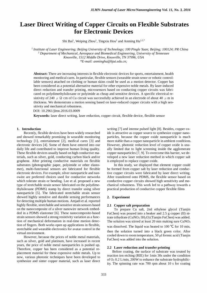
copper salt. To write the copper circuit, a continuous wave diode laser (K808DAECN-30.00W, BWT Beijing LTD.) with a wavelength 808 nm was used. The laser beam spot with about 150 μm diameter (1/e2) was focused by a micro-scope objective (NA=0.3). The scanning speed was 5 mm/s. Figure 1 (a) shows the configuration of the laser direct re-duction system. After laser processing, the specimen was cleaned by DI water in order to wipe off the residual copper salt. For patterning on PDMS, the first step is to mix a PDMS pre-polymer and a curing agent (sylgard 184, Dow corning, USA) with a weight ratio of 10: 1. After all bubbles ran off, the mixture was poured over the glass slide. After further curing in a drying oven at 80 ℃ for 4 h, the copper attached PDMS tape with a thickness of 3 mm was detached from the glass as shown in figure 1 (b)
Mirror
Objective2-Axis Platform
Beam Expander
xy
Dropping Curing Peeling
Fig 1. (a) Schematic of the experimental setup for laser direct reduction. (b) Schematic illustration of fabrication of flexible sensor based on copper cir-cuit.
2.3 Characterization High-resolution images of the Cu patterns were observed
by field emission scanning electron microscopy (Hitachi S-4800, Japan). The electric properties were real-time moni-tored by electrochemical workstation (Chenhua CHI 600E, China).
3. Results and discussion
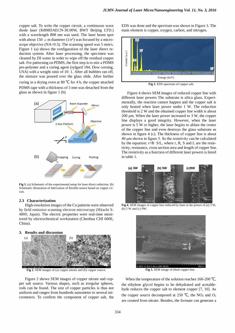
Fig 2. SEM images of (a) copper nitrate and (b) copper source.
Figure 2 shows SEM images of copper nitrate and cop-per salt source. Various shapes, such as irregular spheres, rods can be found. The size of copper particles is thus not uniform and ranges from hundreds nanometer to several mi-crometers. To confirm the component of copper salt, the
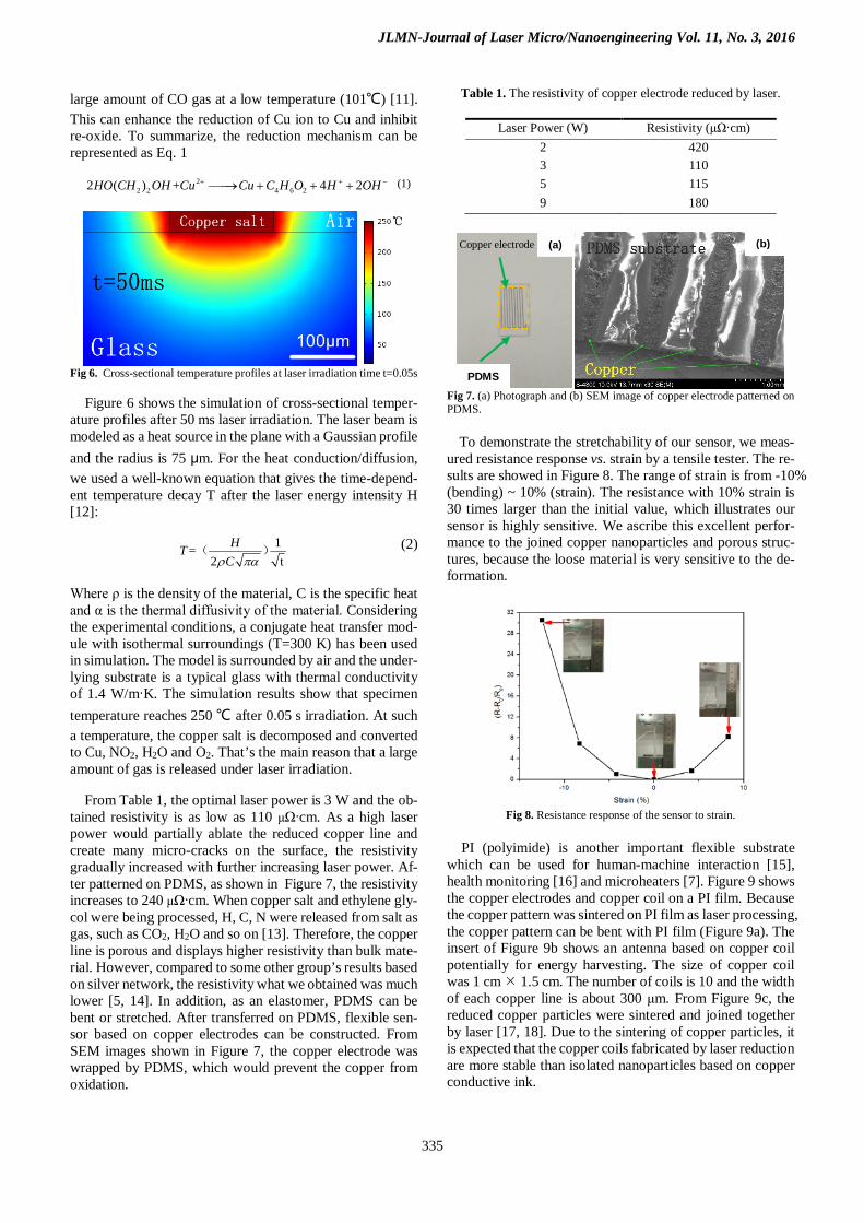
EDS was done and the spectrum was shown in Figure 3. The main element is copper, oxygen, carbon, and nitrogen.
Fig 3. EDS spectrum of copper salt.
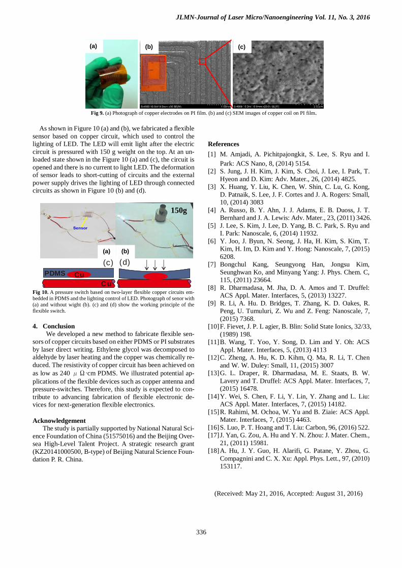
Figure 4 shows SEM images of reduced copper line with different laser powers The substrate is silica glass. Experi-mentally, the reaction cannot happen and the copper salt is only heated when laser power under 1 W. The reduction threshold is 2 W and the obtained copper line width is about 200 μm. When the laser power increased to 3 W, the copper line displays a good integrity. However, when the laser power is 5 W or higher, the laser begins to ablate the center of the copper line and even destroys the glass substrate as shown in figure 4 (c). The thickness of copper line is about 40 μm shown in figure 5. So the resistivity can be calculated by the equation: r=R S/L, where r, R, S and L are the resis-tivity, resistance, cross section area and length of copper line. The resistivity as a function of different laser powers is listed in table 1.
Fig 4. SEM images of copper line reduced by laser at the power of (a) 3 W, (b) 5 W and (c) 9W.
Fig 5. SEM image of tilted copper line.
When the temperature of the solution reaches 160-200 ℃, the ethylene glycol begins to be dehydrated and acetalde-hyde reduces the copper salt to element copper [7, 10]. As the copper source decomposed at 250 ℃, the NO2 and O2 are created from nitrate. Besides, the formate can generate a
Energy (keV)
Coun
ts (a
.u.)
(b)
(a)
(a) (b)
(a) 3W (b) 5W (c)9W
JLMN-Journal of Laser Micro/Nanoengineering Vol. 11, No. 3, 2016
335
large amount of CO gas at a low temperature (101℃) [11]. This can enhance the reduction of Cu ion to Cu and inhibit re-oxide. To summarize, the reduction mechanism can be represented as Eq. 1
22 2 4 6 22 ( ) + 4 2HO CH OH Cu Cu C H O H OH+ + −→ + + + (1)
Fig 6. Cross-sectional temperature profiles at laser irradiation time t=0.05s
Figure 6 shows the simulation of cross-sectional temper-ature profiles after 50 ms laser irradiation. The laser beam is modeled as a heat source in the plane with a Gaussian profile and the radius is 75 μm. For the heat conduction/diffusion, we used a well-known equation that gives the time-depend-ent temperature decay T after the laser energy intensity H [12]:
1=2 t
HTCρ πα
( ) (2)
Where ρ is the density of the material, C is the specific heat and α is the thermal diffusivity of the material. Considering the experimental conditions, a conjugate heat transfer mod-ule with isothermal surroundings (T=300 K) has been used in simulation. The model is surrounded by air and the under-lying substrate is a typical glass with thermal conductivity of 1.4 W/mK. The simulation results show that specimen temperature reaches 250 ℃ after 0.05 s irradiation. At such a temperature, the copper salt is decomposed and converted to Cu, NO2, H2O and O2. That’s the main reason that a large amount of gas is released under laser irradiation.
From Table 1, the optimal laser power is 3 W and the ob-tained resistivity is as low as 110 μΩcm. As a high laser power would partially ablate the reduced copper line and create many micro-cracks on the surface, the resistivity gradually increased with further increasing laser power. Af-ter patterned on PDMS, as shown in Figure 7, the resistivity increases to 240 μΩcm. When copper salt and ethylene gly-col were being processed, H, C, N were released from salt as gas, such as CO2, H2O and so on [13]. Therefore, the copper line is porous and displays higher resistivity than bulk mate-rial. However, compared to some other group’s results based on silver network, the resistivity what we obtained was much lower [5, 14]. In addition, as an elastomer, PDMS can be bent or stretched. After transferred on PDMS, flexible sen-sor based on copper electrodes can be constructed. From SEM images shown in Figure 7, the copper electrode was wrapped by PDMS, which would prevent the copper from oxidation.
Table 1. The resistivity of copper electrode reduced by laser.
Laser Power (W) Resistivity (μΩcm) 2 420 3 110 5 115 9 180
Fig 7. (a) Photograph and (b) SEM image of copper electrode patterned on PDMS.
To demonstrate the stretchability of our sensor, we meas-ured resistance response vs. strain by a tensile tester. The re-sults are showed in Figure 8. The range of strain is from -10% (bending) ~ 10% (strain). The resistance with 10% strain is 30 times larger than the initial value, which illustrates our sensor is highly sensitive. We ascribe this excellent perfor-mance to the joined copper nanoparticles and porous struc-tures, because the loose material is very sensitive to the de-formation.
Fig 8. Resistance response of the sensor to strain.
PI (polyimide) is another important flexible substrate which can be used for human-machine interaction [15], health monitoring [16] and microheaters [7]. Figure 9 shows the copper electrodes and copper coil on a PI film. Because the copper pattern was sintered on PI film as laser processing, the copper pattern can be bent with PI film (Figure 9a). The insert of Figure 9b shows an antenna based on copper coil potentially for energy harvesting. The size of copper coil was 1 cm 1.5 cm. The number of coils is 10 and the width of each copper line is about 300 μm. From Figure 9c, the reduced copper particles were sintered and joined together by laser [17, 18]. Due to the sintering of copper particles, it is expected that the copper coils fabricated by laser reduction are more stable than isolated nanoparticles based on copper conductive ink.
Copper electrode (a) (b)
PDMS
JLMN-Journal of Laser Micro/Nanoengineering Vol. 11, No. 3, 2016
336
Fig 9. (a) Photograph of copper electrodes on PI film. (b) and (c) SEM images of copper coil on PI film.
As shown in Figure 10 (a) and (b), we fabricated a flexible sensor based on copper circuit, which used to control the lighting of LED. The LED will emit light after the electric circuit is pressured with 150 g weight on the top. At an un-loaded state shown in the Figure 10 (a) and (c), the circuit is opened and there is no current to light LED. The deformation of sensor leads to short-cutting of circuits and the external power supply drives the lighting of LED through connected circuits as shown in Figure 10 (b) and (d).
PDMSCu
Cu(c) (d)
Fig 10. A pressure switch based on two-layer flexible copper circuits em-bedded in PDMS and the lighting control of LED. Photograph of senor with (a) and without wight (b). (c) and (d) show the working principle of the flexible switch.
4. Conclusion We developed a new method to fabricate flexible sen-
sors of copper circuits based on either PDMS or PI substrates by laser direct writing. Ethylene glycol was decomposed to aldehyde by laser heating and the copper was chemically re-duced. The resistivity of copper circuit has been achieved on as low as 240 μΩcm PDMS. We illustrated potential ap-plications of the flexible devices such as copper antenna and pressure-switches. Therefore, this study is expected to con-tribute to advancing fabrication of flexible electronic de-vices for next-generation flexible electronics.
Acknowledgement The study is partially supported by National Natural Sci-
ence Foundation of China (51575016) and the Beijing Over-sea High-Level Talent Project. A strategic research grant (KZ20141000500, B-type) of Beijing Natural Science Foun-dation P. R. China.
References [1] M. Amjadi, A. Pichitpajongkit, S. Lee, S. Ryu and I.
Park: ACS Nano, 8, (2014) 5154. [2] S. Jung, J. H. Kim, J. Kim, S. Choi, J. Lee, I. Park, T.
Hyeon and D. Kim: Adv. Mater., 26, (2014) 4825. [3] X. Huang, Y. Liu, K. Chen, W. Shin, C. Lu, G. Kong,
D. Patnaik, S. Lee, J. F. Cortes and J. A. Rogers: Small, 10, (2014) 3083
[4] A. Russo, B. Y. Ahn, J. J. Adams, E. B. Duoss, J. T. Bernhard and J. A. Lewis: Adv. Mater., 23, (2011) 3426.
[5] J. Lee, S. Kim, J. Lee, D. Yang, B. C. Park, S. Ryu and I. Park: Nanoscale, 6, (2014) 11932.
[6] Y. Joo, J. Byun, N. Seong, J. Ha, H. Kim, S. Kim, T. Kim, H. Im, D. Kim and Y. Hong: Nanoscale, 7, (2015) 6208.
[7] Bongchul Kang, Seungyong Han, Jongsu Kim, Seunghwan Ko, and Minyang Yang: J. Phys. Chem. C, 115, (2011) 23664.
[8] R. Dharmadasa, M. Jha, D. A. Amos and T. Druffel: ACS Appl. Mater. Interfaces, 5, (2013) 13227.
[9] R. Li, A. Hu. D. Bridges, T. Zhang, K. D. Oakes, R. Peng, U. Tumuluri, Z. Wu and Z. Feng: Nanoscale, 7, (2015) 7368.
[10] F. Fievet, J. P. L agier, B. Blin: Solid State Ionics, 32/33, (1989) 198.
[11] B. Wang, T. Yoo, Y. Song, D. Lim and Y. Oh: ACS Appl. Mater. Interfaces, 5, (2013) 4113
[12] C. Zheng, A. Hu, K. D. Kihm, Q. Ma, R. Li, T. Chen and W. W. Duley: Small, 11, (2015) 3007
[13] G. L. Draper, R. Dharmadasa, M. E. Staats, B. W. Lavery and T. Druffel: ACS Appl. Mater. Interfaces, 7, (2015) 16478.
[14] Y. Wei, S. Chen, F. Li, Y. Lin, Y. Zhang and L. Liu: ACS Appl. Mater. Interfaces, 7, (2015) 14182.
[15] R. Rahimi, M. Ochoa, W. Yu and B. Ziaie: ACS Appl. Mater. Interfaces, 7, (2015) 4463.
[16] S. Luo, P. T. Hoang and T. Liu: Carbon, 96, (2016) 522. [17] J. Yan, G. Zou, A. Hu and Y. N. Zhou: J. Mater. Chem.,
21, (2011) 15981. [18] A. Hu, J. Y. Guo, H. Alarifi, G. Patane, Y. Zhou, G.
Compagnini and C. X. Xu: Appl. Phys. Lett., 97, (2010) 153117.
(a) (b) (c)
150g
(a) (b)
(Received: May 21, 2016, Accepted: August 31, 2016)