Embed Size (px)
Citation preview

Pat PhotongkamResearch Facility DivisionSynchrotron Light Research Institute (Public Organization)
Synchrotron Light Research Institute (Public Organization)111 University Ave. Suranaree Muang Nakhon-Ratchasima THAILAND 30000
PHOTOEMISSIONELECTRON
MICROSCOPY
PEEM is the full field imaging that utilizes emitted electrons from specimen absorbing photon energy to generate image of its surface
Synchrotron radiation based PEEM (SR-PEEM) is spectro-microscopic technique with chemical, magnetic andelectronic structure sensitivities, based on well known spectroscopic methods of
X-ray absorption spectroscopy (XAS)
Photoemission Spectroscopy (PES)
2
Photoemission Electron Microscopy (PEEM)
Photoelectric Effect
Cathode Lens Microscopy
Basic Principle
Photoemission Electron Microscopy (PEEM)

Photoemission Electron Microscopy (PEEM)
3
Photoemission Electron Microscopy
Photoemission• ultra-violet (UV) or soft X-ray
Cathode / Immersions lens• Electrons are accelerated by
strong electric field and turned into magnified image
Image column• image is further magnified
by set of additional lenses onto screen
2D image detector• e.g. a multi-channel
plate (MCP) intensifier
- HV GND GND
In photoelectric effect, electrons are ejected from atom by which photon energy is completely absorbed upon exposure to electromagnetic radiation. (dominant for hv ≤ 50 keV)
Photoemission Electron Microscopy (PEEM)
4
Photoelectric Effect
The intensity of emitted electrons is responsive to
photon energy and flux
chemical, electronic and local structure
The energy of emitted electron depends on their origin which is
Photoelectrons
Auger electrons
Secondary electron

Photoelectron
electrons in orbital are ejected to continuum by primary radiation
Photoemission Electron Microscopy (PEEM)
5
Photoelectric Effect
Kinetic Energy
Elec
tron
Cou
nt
. . . .K E hv B E
Secondary electron
generated by energetic electrons interact to other electrons
sensitive to electron transition & scattering of photoelectron wave
Auger electrons
electrons in orbital are ejected by secondary radiation
elemental unique energy profile
an element specific characterization for electronic structure and local geometric of matter
The measurement of linear absorption coefficient as function of photon energy is sensitive to
Element and chemical state Valence state, bond orientation,
nearest-neighbour Final state Magnetic order
6
X-ray Absorption Spectroscopy (XAS)
( )0
E xI I e
Photoemission Electron Microscopy (PEEM)

In PES, it measures the energy distribution of the photoemitted electron from the specimen
Features
highest surface sensitivity
Elemental and chemical sensitivity (core level shifts)
electronic structure sensitivity
Photoemission Electron Microscopy (PEEM)
7
Photoemission Spectroscopy (PES)
Electron Inelastic Mean Free Path (“universal curve”)
an index of how far an electron on average travels through matter before losing energy
Photoemission Electron Microscopy (PEEM)
8
Inelastic Mean Free Path

The probability per unit area, per unit time that a photon of a given energy can be absorbed by an atom to excite the photoelectrons.
Photoemission Electron Microscopy (PEEM)
9
Photoionization cross section
( )( )
( )
P hvhv
I hv
# photon absorbed per unit time
Incident Photon Flux
Cross section
Photoemission Electron Microscopy (PEEM)
10
Photoemission Electron Microscopy (PEEM)
Image contrast in PEEM arise from the variation in electron emission which is sensitive to surface topography, chemical state, magnetic order and electronic structure
1. Topographic contrast
• electron deflection due to roughness and structure surface
Corresponding PEEM Image
Topographic feature
2. Work function contrast
Sub ML quantities of Cu on Si(100)
Pentacene Molecules on Si

Photoemission Electron Microscopy (PEEM)
11
Photoemission Electron Microscopy (PEEM)
3. Chemical contrast
XAS can be implemented by measuring intensity of secondary electron yield from the image as a function of photon energy
PES requires energy analyser/filter to implement by these following methods
i. measuring intensity of image as function of electron energy
ii. Imaging on energy dispersion plane at exit of analyser
Photoemission Electron Microscopy (PEEM)
12
XAS and PES with SR-PEEMX-ray Absorption Spectroscopy Photoemission Spectroscopy

4. Magnetic contrast
Photoemission Electron Microscopy (PEEM)
13
Photoemission Electron Microscopy (PEEM)
Photoemission Electron Microscopy (PEEM)
14
XMCD & XMLD
X-ray Magnetic Circular Dichroism (XMCD): Ferromagnetism
X-ray Magnetic Linear Dichroism (XMCD): Anti-ferromagnetism

Photoemission Electron Microscopy (PEEM)
15
PEEM Instrument
Elmitec PEEM III
Photoemission Electron Microscopy (PEEM)
16
PEEM Instrument

Photoemission Electron Microscopy (PEEM)
17
PEEM Instrument
Photoemission Electron Microscopy (PEEM)
18
PEEM Instrument

Photoemission Electron Microscopy (PEEM)
19
PEEM Instrument
RLIN
IN ACL P2 P3
detector
P1 IL FL TLOBJ
specimen
projective
transfer optic
hν
analyzer
imaging column
LaB6 e-gun
illumination column
field limiting aperture (FLA)angle limiting aperture (ALA) electron analyzer exit slitdiffraction plane (crossover)image plane
Photoemission Electron Microscopy (PEEM)
20
PEEM Instrument

Spectroscopic Imaging
Photoemission Electron Microscopy (PEEM)
21
Photoemission Electron Microscopy (PEEM)
Microprobe diffraction Microprobe-spectroscopy
Reciprocal space(diffraction plane)
Energy dispersion(dispersive plane)
Real space(image plane)
PED / µ-ARPES PED / µ-ARPESX-PEEM, EF-PEEM
Application of PEEM
700 eV705 eV
710 eV715 eV
720 eV725 eV
700 705 710 715 720 725 730
(E
)
Photon Energy (eV)
X-ray absorption spectroscopy
Photoemission Electron Microscopy (PEEM)
22
700 705 710 715 720 725 730
Intact Corroded
(E
) (a
.u.)
Photon Energy (eV)730 eV
730 eV700 eV

Application of PEEM
Sarayut Tunmee, et.al, Journal of Applied Physics 120, 195303 (2016)
Investigation of pitting corrosion of diamond-like carbon films using synchrotron based spectromicroscopy
Photoemission Electron Microscopy (PEEM)
23
Photoemission Electron Microscopy (PEEM)
24
Application of PEEM
K.E = 75.6eV K.E = 76.8eV
• Photon Energy = 100eV• FOV = 20µm• Energy Slit = 25µm• Contrast aperture = 30µm
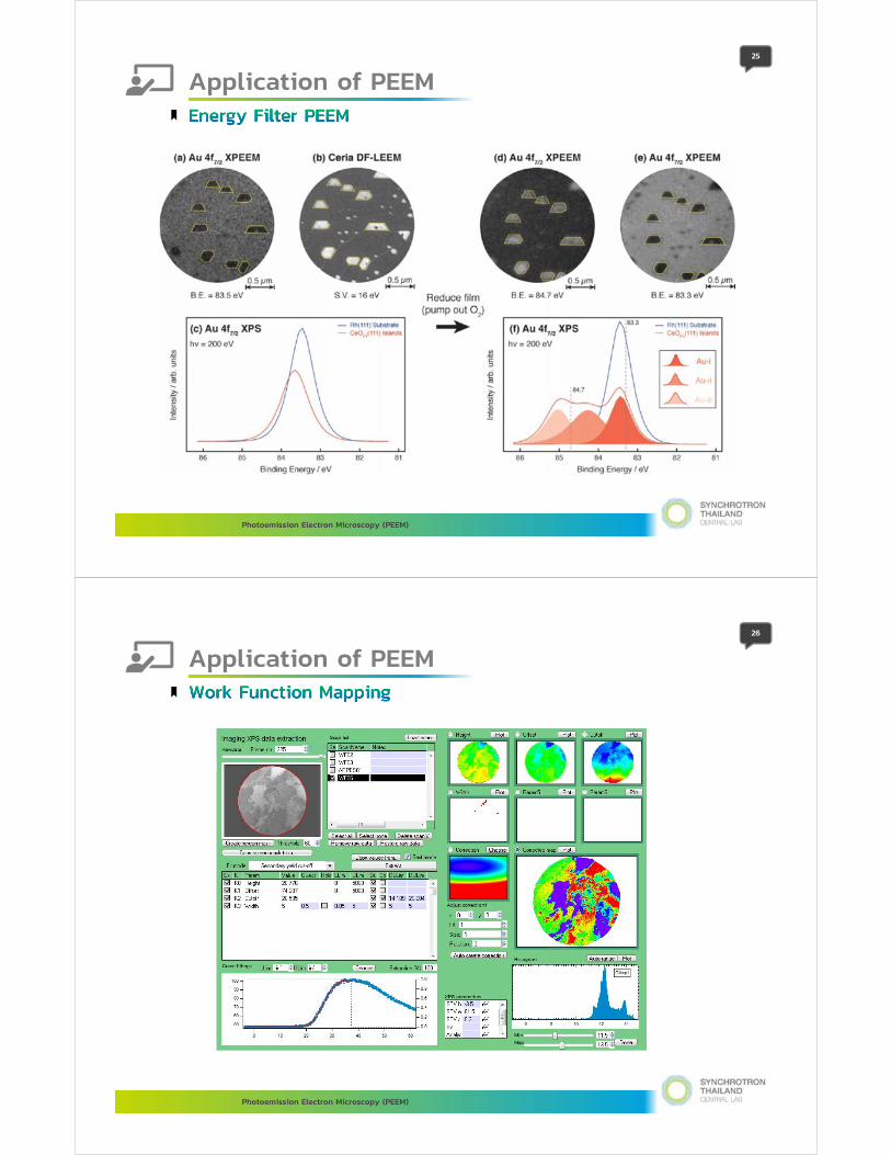
Photoemission Electron Microscopy (PEEM)
25
Application of PEEM
Photoemission Electron Microscopy (PEEM)
26
Application of PEEM

Photoemission Electron Microscopy (PEEM)
27
Application of PEEM
1ML Graphene with 2ML islands grown on SiC (0001)
IBM J. Res. & Dev. 55, 6 (2011)
The PED (µARPES) taken from 1 ML Grahpene and 2ML islands are shown on the right. High energy resolution 2-D (kx,ky) maps for 1-ML and 2-ML graphene taken at an electron binding energy of 2.5 eV below the Fermi level. 2π-bands are clearly seen from the two-ML island. The profile of π-bands also illustrates the resolution of PED in k-space.
hv = 35eV, Ebin = 2.5eV.
Photoemission Electron Microscopy (PEEM)
28
Application of PEEM

Photoemission Electron Microscopy (PEEM)
29
Application of PEEM
W{110} clean surface
W 4f core level
Photon energy = 131 eV
Photoemission Electron Microscopy (PEEM)
30
Application of PEEM

Photon polarization of this beamline is horizontally linear – therefore it is NOT possible for XMCD, XMLD, and magnetic contrast imaging
End station is also equipped with ion sputtering gun and residual gas analyser
31
BL3.2Ub: PEEM at SLRI
Technical information
source planar halbach-type undulator (U60)41 periods. 0.5467 Tesla at gap 26.5mm
monochromator & energy range
varied line spacing plane grating40-160eV and 220-1040eV
energy resolution & flux
ΔE/E =10-5 at 100eVflux: 1010 photons/sec
beam size (HxV) 0.8 mm x 0.1 mm
end station Elmitec SPELEEM
Technique XAS, PES, APRESMEM, LEEM, LEED
Photoemission Electron Microscopy (PEEM)
LEEM is a cathode lens microscopy technique which probes surfaces and interfaces with low energy electrons, using the elastically backscattered beam for imaging.
LEEM is particularly well suited to monitor dynamic processes, such as surface reconstructions, epitaxial growth, step dynamics, self-organization
Photoemission Electron Microscopy (PEEM)
32
Low Energy Electron Microscopy
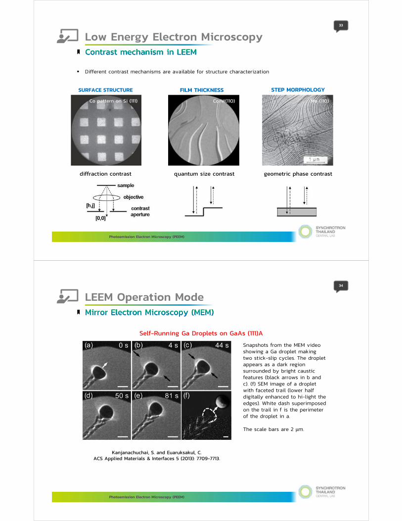
Different contrast mechanisms are available for structure characterization
Photoemission Electron Microscopy (PEEM)
33
Low Energy Electron Microscopy
diffraction contrast
FILM THICKNESS STEP MORPHOLOGYSURFACE STRUCTURE
quantum size contrast geometric phase contrast
Co/W(110) Mo (110)Co pattern on Si (111)
LEEM Operation Mode
Self-Running Ga Droplets on GaAs (111)ASnapshots from the MEM video showing a Ga droplet making two stick-slip cycles. The droplet appears as a dark region surrounded by bright caustic features (black arrows in b and c). (f) SEM image of a droplet with faceted trail (lower half digitally enhanced to hi-light the edges). White dash superimposed on the trail in f is the perimeter of the droplet in a. The scale bars are 2 µm.
Kanjanachuchai, S. and Euaruksakul, C. ACS Applied Materials & Interfaces 5 (2013): 7709-7713.
Photoemission Electron Microscopy (PEEM)
34
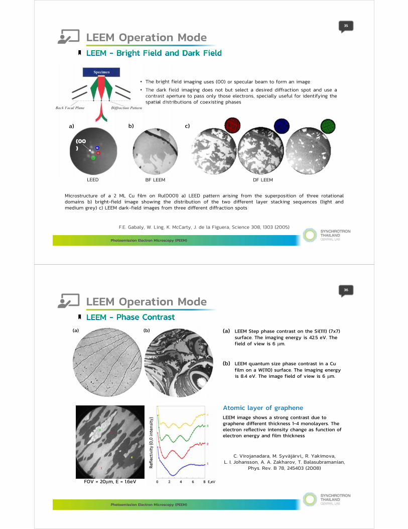
LEEM Operation Mode
• The bright field imaging uses (00) or specular beam to form an image• The dark field imaging does not but select a desired diffraction spot and use a
contrast aperture to pass only those electrons, specially useful for identifying thespatial distributions of coexisting phases
Microstructure of a 2 ML Cu film on Ru(0001) a) LEED pattern arising from the superposition of three rotationaldomains b) bright-field image showing the distribution of the two different layer stacking sequences (light andmedium grey) c) LEEM dark-field images from three different diffraction spots
LEED BF LEEM DF LEEM
F.E. Gabaly, W. Ling, K. McCarty, J. de la Figuera, Science 308, 1303 (2005)
(00)
a) b) c)
Photoemission Electron Microscopy (PEEM)
35
LEEM Operation Mode
Atomic layer of graphene LEEM image shows a strong contrast due to graphene different thickness 1-4 monolayers. The electron reflective intensity change as function of electron energy and film thickness
FOV = 20µm, E = 1.6eV
(b) LEEM quantum size phase contrast in a Cu film on a W(110) surface. The imaging energy is 8.4 eV. The image field of view is 6 µm.
(a) LEEM Step phase contrast on the Si(111) (7x7) surface. The imaging energy is 42.5 eV. The field of view is 6 µm.
(a) (b)
C. Virojanadara, M. Syväjärvi,, R. Yakimova, L. I. Johansson, A. A. Zakharov, T. Balasubramanian,
Phys. Rev. B 78, 245403 (2008)
Photoemission Electron Microscopy (PEEM)
36

LEEM Operation Mode
Epitaxial grown pentacene on the h-BN nanomesh
Substrate: BN nanomesh grown on Rh(111) crystal
LEED pattern of pentacene 1st layer comparing to the substrate
LEEM image: FOV=20µm, E = 3.4 eV
Photoemission Electron Microscopy (PEEM)
37
SR-PEEM or X-PEEM is widely used technique in synchrotron facilities for imaging a surface of materials with chemical, magnetic and electronic structure sensitivity.
It is surface sensitive spectro-microscopy based on X-ray absorption (XAS) and photoemission spectroscopy (PES)
UV and soft X-ray is usual source for X-PEEM. Hard x-ray is possible but photoionization cross section is much lower at high photon energy
The sample for PEEM should be smooth and flat – to minimize topographic effect and to enhance lateral resolution.
Switchable photon polarization make X-PEEM become more powerful – magnetic properties study
38
Summary
Photoemission Electron Microscopy (PEEM)