Embed Size (px)
Citation preview

Ph.D. THESIS
Investigation of atomic-sized conductors with the
mechanically controllable break junction technique
Andras HALBRITTER
Supervisor: Prof. Gyorgy MIHALY
Budapest University of Technology
and Economics
Institute of Physics
Department of Physics
BUTE
2003

Contents
1 Introduction 4
2 Overview of the research field 6
2.1 Fabrication techniques . . . . . . . . . . . . . . . . . . . . . . . . . . . . . 7
2.2 Theory of point contacts . . . . . . . . . . . . . . . . . . . . . . . . . . . . 9
2.2.1 Diffusive point contacts . . . . . . . . . . . . . . . . . . . . . . . . . 10
2.2.2 Ballistic point contacts . . . . . . . . . . . . . . . . . . . . . . . . . 10
2.2.3 Intermediate region . . . . . . . . . . . . . . . . . . . . . . . . . . . 13
2.3 Ballistic transport in quantum wires . . . . . . . . . . . . . . . . . . . . . 14
2.3.1 The Landauer formalism . . . . . . . . . . . . . . . . . . . . . . . . 14
2.3.2 Conductance quantization . . . . . . . . . . . . . . . . . . . . . . . 16
2.4 Atomic-sized conductors . . . . . . . . . . . . . . . . . . . . . . . . . . . . 19
2.4.1 Exploring the conductance eigenchannels of single atoms . . . . . . 22
2.4.2 Formation of atomic chains . . . . . . . . . . . . . . . . . . . . . . 25
3 Experimental techniques 27
3.1 Principles of the MCBJ technique . . . . . . . . . . . . . . . . . . . . . . . 27
3.2 Sample preparation . . . . . . . . . . . . . . . . . . . . . . . . . . . . . . . 31
3.3 The sample holder . . . . . . . . . . . . . . . . . . . . . . . . . . . . . . . 33
3.4 The way of the measurements . . . . . . . . . . . . . . . . . . . . . . . . . 37
3.4.1 Conductance traces and the calibration of the electrode separation . 38
3.4.2 Building conductance histograms . . . . . . . . . . . . . . . . . . . 41
3.4.3 Recording I-V curves . . . . . . . . . . . . . . . . . . . . . . . . . . 43
4 Transition from direct contact to tunneling in tungsten 46
4.1 Introduction . . . . . . . . . . . . . . . . . . . . . . . . . . . . . . . . . . . 46
4.2 Experimental details . . . . . . . . . . . . . . . . . . . . . . . . . . . . . . 48
4.3 The nature of conductance traces in tungsten contacts . . . . . . . . . . . 48
4.4 Discussion of the results . . . . . . . . . . . . . . . . . . . . . . . . . . . . 53
2

CONTENTS 3
4.5 Conclusions . . . . . . . . . . . . . . . . . . . . . . . . . . . . . . . . . . . 58
5 Locally overheated point contacts 59
5.1 Introduction . . . . . . . . . . . . . . . . . . . . . . . . . . . . . . . . . . . 59
5.2 Predictions for the temperature of nanocontacts at elevated bias voltage . . 60
5.3 Experimental details . . . . . . . . . . . . . . . . . . . . . . . . . . . . . . 63
5.4 The saturation of the conductance traces at elevated bias voltage . . . . . 63
5.5 Conclusions . . . . . . . . . . . . . . . . . . . . . . . . . . . . . . . . . . . 67
6 Nonlinear conductance in atomic-sized junctions 68
6.1 Introduction . . . . . . . . . . . . . . . . . . . . . . . . . . . . . . . . . . . 68
6.2 Experimental details . . . . . . . . . . . . . . . . . . . . . . . . . . . . . . 69
6.3 Quantum interference effects . . . . . . . . . . . . . . . . . . . . . . . . . . 71
6.3.1 The influence of quantum interference on the slope of the conduc-
tance plateaus . . . . . . . . . . . . . . . . . . . . . . . . . . . . . . 72
6.3.2 Considerations about the problem of decoherence . . . . . . . . . . 75
6.3.3 Differential conductance curves in other metals . . . . . . . . . . . 77
6.4 Voltage dependence of the bare transmission of the junction . . . . . . . . 77
6.4.1 Thermal expansion of the electrodes . . . . . . . . . . . . . . . . . 80
6.5 Conclusions . . . . . . . . . . . . . . . . . . . . . . . . . . . . . . . . . . . 82
7 Hydrogen-assisted distortion of gold nanowires 84
7.1 Introduction . . . . . . . . . . . . . . . . . . . . . . . . . . . . . . . . . . . 84
7.2 Experimental details . . . . . . . . . . . . . . . . . . . . . . . . . . . . . . 85
7.3 Basic observation: the appearance of a new peak in the conductance his-
togram . . . . . . . . . . . . . . . . . . . . . . . . . . . . . . . . . . . . . . 86
7.4 The nature of the conductance traces . . . . . . . . . . . . . . . . . . . . . 88
7.5 Exploring correlations between the peaks in the histogram . . . . . . . . . 89
7.6 Plateau length histograms . . . . . . . . . . . . . . . . . . . . . . . . . . . 91
7.7 Discussion of the observations . . . . . . . . . . . . . . . . . . . . . . . . . 92
Conclusions 94
List of publications 96
Acknowledgements 98
References 99

Chapter 1
Introduction
In the recent decades the development of nanotechnology has opened the possibility of
exploring the matter on a previously unaccessible length-scale. A new chapter of physics
has been introduced investigating mesoscopic systems, which are “neither too large, nor
too small”. It turned out that the knowledge about single atoms and macroscopic solids
can hardly be synthesized to understand the systems of intermediate size.
The establishment of two dimensional electron gas (2DEG) in semiconductor het-
erostructures has played a key role in the technological development. The highly enhanced
Fermi wavelength of electrons (≈ 40 nm) in a 2DEG became comparable to the resolution
of nanolithography, so with the proper preparation of gate electrodes artificial quantum
confinement of electrons could be established. The quantum mechanical motion of elec-
trons in such devices allows the investigation of various coherent quantum phenomena,
like quantum Hall effect [1], Coulomb blockage [2] and conductance quantization [3, 4].
Another crucial experimental achievement was the development of the scanning tun-
neling microscope (STM) and other scanning probe techniques [5]. These devices have
stimulated a new field called nanophysics, referring to the investigation of the matter
on the atomic scale. The fundamental application of the STM is the study of surface
topography in the non-contact scanning mode, but it was discovered soon that the probe
tip can also be used to modify the surface or even to build artificial structure of atoms
[6]. The mechanical behavior of the material on such scale has demonstrated several in-
teresting features. For instance, a nanowire can be pulled out of the sample surface if the
tip is intentionally pushed into the sample and thereafter retracted back. This nanowire
becomes narrower and narrower during its elongation, and before the complete rupture a
single atom connects the two sides.
The investigation of the mechanical and electrical properties of such “nanocontacts”
has recently became an interesting topic of nanoscience [7]. As the Fermi wavelength
4

INTRODUCTION 5
of electrons in a metal is in the order of the interatomic spacing (≈ 3 A), these atomic
contacts can also be considered as quantum confined systems. In such nanojunctions the
coherent quantum phenomena always interplay with the atomic granularity of the matter,
which makes the understanding of the experimental observations less straightforward.
This thesis presents an experimental study of atomic-sized contacts in various systems.
The measurements were performed with the so-called mechanically controllable break
junction (MCBJ) technique, a simple method for creating highly stable nanojunctions.
After giving a brief overview of the research field in Chap. 2 the principles of the MCBJ
technique and the design of the applied sample holder are introduced in Chap. 3. The
remaining part of the thesis presents my experimental results, divided into four parts. In
Chap. 4 the special mechanical behavior of tungsten nanocontacts is studied. The next
part (Chap. 5) investigates the dynamical motion of atoms in locally overheated lead
and aluminum nanojunctions. The third group of measurements examines the origin of
nonlinear conductance in various sample material (Chap. 6). Finally, the last part reports
about the hydrogen assisted distortion of gold nanowires (Chap. 7).

Chapter 2
Overview of the research field
Metallic systems, where two macroscopic electrodes are connected via a contact with small
cross section have been studied long before the explosive development of nanoscience.
These systems are called “point contacts” (PC) in general, regardless of the actual size
of the contact area. It can be generally stated, that the resistance of a point contact is
mostly determined by the narrow neighborhood of the junction; therefore, a PC acts as
a “microscope” magnifying all kinds of phenomena occurring in the small contact region.
A more detailed description of this phenomenon is given in Sec. 2.2, including the physics
of ballistic and diffusive point contacts.
The next part (Sec. 2.3) describes the transport of electrons in quantum wires with the
methodogy of mesoscopic physics, including the introduction of the Landauer formalism
and the conductance quantization phenomenon.
Both theories are essential to understand the phenomena observed in atomic-sized con-
ductors, described in Sec. 2.4. Here mostly the crucial experimental results are discussed,
including conductance histogram and force measurements, the investigation of individual
conductance channels by various methods and the observation of atomic chain formation.
The aim of this section is to describe the character of conductance through single atoms,
and to draw a picture about the mechanical behavior of contacts on atomic scale.
As this thesis presents an experimental study of atomic-sized point contacts, a fun-
damental importance is attributed to the introduction of the experimental techniques,
which make the preparation of small, even atomic-sized junctions possible. The short
overview of these techniques is taken first in Sec. 2.1, and the theories and experimental
observations are discussed afterwards.
6
OVERVIEW OF THE RESEARCH FIELD 7
(a) (b)
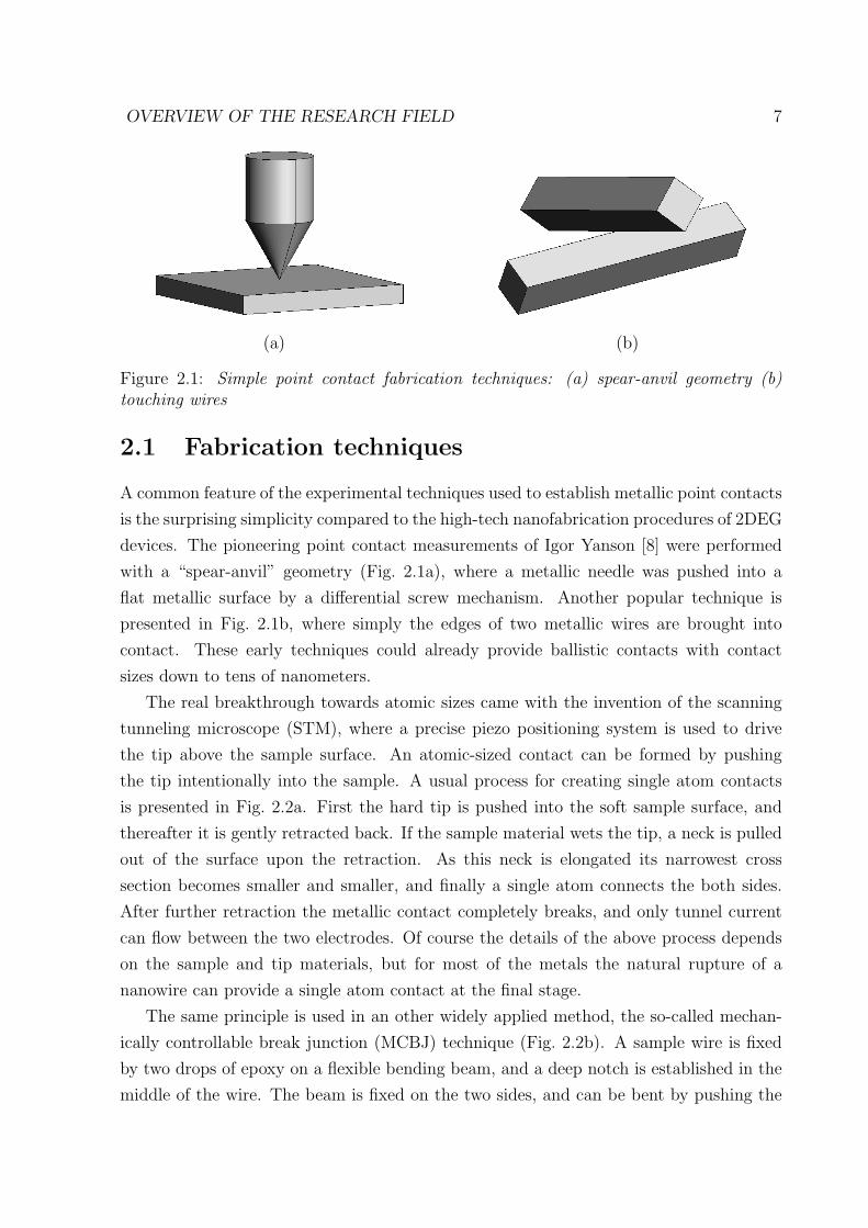
Figure 2.1: Simple point contact fabrication techniques: (a) spear-anvil geometry (b)touching wires
2.1 Fabrication techniques
A common feature of the experimental techniques used to establish metallic point contacts
is the surprising simplicity compared to the high-tech nanofabrication procedures of 2DEG
devices. The pioneering point contact measurements of Igor Yanson [8] were performed
with a “spear-anvil” geometry (Fig. 2.1a), where a metallic needle was pushed into a
flat metallic surface by a differential screw mechanism. Another popular technique is
presented in Fig. 2.1b, where simply the edges of two metallic wires are brought into
contact. These early techniques could already provide ballistic contacts with contact
sizes down to tens of nanometers.
The real breakthrough towards atomic sizes came with the invention of the scanning
tunneling microscope (STM), where a precise piezo positioning system is used to drive
the tip above the sample surface. An atomic-sized contact can be formed by pushing
the tip intentionally into the sample. A usual process for creating single atom contacts
is presented in Fig. 2.2a. First the hard tip is pushed into the soft sample surface, and
thereafter it is gently retracted back. If the sample material wets the tip, a neck is pulled
out of the surface upon the retraction. As this neck is elongated its narrowest cross
section becomes smaller and smaller, and finally a single atom connects the both sides.
After further retraction the metallic contact completely breaks, and only tunnel current
can flow between the two electrodes. Of course the details of the above process depends
on the sample and tip materials, but for most of the metals the natural rupture of a
nanowire can provide a single atom contact at the final stage.
The same principle is used in an other widely applied method, the so-called mechan-
ically controllable break junction (MCBJ) technique (Fig. 2.2b). A sample wire is fixed
by two drops of epoxy on a flexible bending beam, and a deep notch is established in the
middle of the wire. The beam is fixed on the two sides, and can be bent by pushing the

OVERVIEW OF THE RESEARCH FIELD 8
(a) (b)
Figure 2.2: (a) – Cartoon representation of contact fabrication using an STM, taken from[7]. (b) – Mechanically controllable break junction technique. The figure shows a realisticdemonstration of the sample holder used in our measurements.
middle part. For this purpose a combination of a piezo crystal and a differential screw
mechanism is used. As the beam is bent the sample wire breaks between the anchoring
points at the notch. This method does not allow surface scanning as the STM, but it has
a significantly better mechanical stability. The reason for this enhanced stability is the
special mechanical design. Upon a vertical displacement of the piezo positioner, ∆z the
electrodes experience a horizontal displacement, ∆x, which can be hundred times smaller
than ∆z. Therefore, any mechanical vibration of the sample holder has a strongly reduced
effect on the contact itself. This method is applied in our experiments as well, so a more
detailed description is given in Chap. 3.
The two crucial problems in fabricating atomic-sized contacts is the requirement of
sub-Angstrom mechanical stability, and the elimination of contaminants. Performing the
measurements in liquid Helium cryostats provides perfect circumstances in both respects.
The stable temperature (4.2 K) eliminates any mechanical drifts due to thermal expansions
in the sample holder, and the cryogenic vacuum provides such a clean environment that
is hardly accessible in any room temperature ultra high vacuum (UHV) systems. The
only problem is to create clean electrode surfaces in situ, in the cryvacuum. In the case
of MCBJ technique this problem is naturally solved, as the wire can be broken in-situ,
after cooling down the whole system.
Using the MCBJ technique or high stability helium temperature STMs single atom
contacts can survive for several hours. In room temperature measurements usually just
transient processes can be observed, and high-speed data acquisition is required to monitor
the behavior of the contact.

OVERVIEW OF THE RESEARCH FIELD 9
(a) (b) (c)
Figure 2.3: Three point contact models. (a) An orifice with diameter “d” in an insulatingscreen between two metallic half-spaces. (b) Two bulk regions are connected with a long,narrow conducting neck. (c) Rotational hyperboloid.
2.2 Theory of point contacts
Theoretically, point-contacts are considered as two bulk electrodes connected through
a narrow constriction. The simplest, and most commonly used PC model is presented
in Fig. 2.3a. This so-called opening-like point contact is an orifice with diameter d in
an infinite isolating plane between the two electrodes. Another extreme limit is the
channel-like PC: a long, narrow neck between the bulk regions with the length being
much larger than the diameter, L d (Fig. 2.3b). The crossover between the both
cases can be obtained by considering the point-contacts as rotational hyperboloids with
different opening angles (Fig. 2.3c). In most of the cases the shape of the PC does not
influence the character of physical processes in the constriction radically, and the main
parameter is the ratio of the contact diameter (d) and other characteristic length scales
in the system. Three fundamental length scales are the mean free paths connected to
different scattering processes (l); the Fermi wavelength of electrons (λF ); and the atomic
diameter (da).
If the Fermi wavelength or the atomic diameter becomes comparable to the contact
size, we speak about quantum point contacts and atomic-sized point contacts, respectively.
These systems are subjects of detailed discussion in the following sections. In this section
we consider contacts, that are neither atomic nor quantum, but that are small enough
compared to certain mean free paths.
Concerning the mean free paths, we have to make difference between the elastic and
inelastic scatterings. Under usual experimental conditions the elastic mean free path (le)
is smaller than the inelastic one (li). Here the inelastic mean free path is the length
of the path an electron travels between two inelastic scatterings (li = vF τi). Mostly

OVERVIEW OF THE RESEARCH FIELD 10
the important parameter is not li, but the inelastic diffusive length, that is the average
distance an electron can diffuse between two inelastic scatterings: Li =√
lile. If the
contact diameter is much smaller than any of the mean free paths d le, li, we speak
about a ballistic contact. In this case the electron travels through the the constriction
without any scattering (except for the reflection on the walls). On the other hand, if
d le, the electron makes a diffusive motion in the contact, and accordingly we speak
about the diffusive regime. At contact diameters exceeding the inelastic diffusive length
(d Li) the excess energy of the electrons is dissipated inside the constriction, which
causes a considerable Joule heating in the contact. This limit is called thermal regime.
In the following subsections the diffusive and ballistic contacts are discussed. Some
details about the thermal regime are presented in Chap. 5.
2.2.1 Diffusive point contacts
A diffusive point contact is described by Maxwell’s equations. The current density in
the sample is always proportional to the electric field: j(r) = σE(r), and the potential
fulfils the Laplace equation: Φ(r) = 0 due to the charge neutrality in metals. Actually,
Maxwell himself was the first who calculated the exact resistance of an orifice-like PC [9].
The Laplace equation can be solved in a hyperbolic coordinate system [10], giving the
following simple formula for the resistance of a diffusive point contact:
R =1
σd, (2.1)
where σ is the conductivity of the metal. The value of the potential along the contact
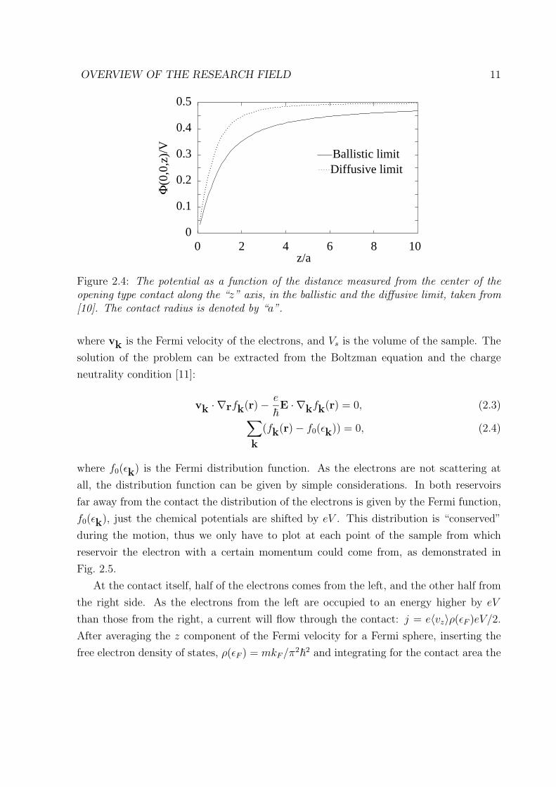
axis is presented in Fig. 2.4, demonstrating that the main part of the potential drops in
the contact region, within a distance in the order of the contact diameter.
2.2.2 Ballistic point contacts
In the ballistic limit the electrons are travelling along straight trajectories, and in the first
approximation no scatterings are taken into consideration. This system is described by the
equations of semiclassical dynamics, so the place and momentum dependent distribution
function, fk(r) is to be determined beside the electric potential, Φ(r). The current density
is written as:
j(r) =2e
Vs
∑k
vkfk(r), (2.2)
OVERVIEW OF THE RESEARCH FIELD 11
Φ(0
,0,z
)/V
0
0.1
0.2
0.3
0.4
0.5
0 2 4 6 8 10
Ballistic limitDiffusive limit
z/a
Figure 2.4: The potential as a function of the distance measured from the center of theopening type contact along the “z” axis, in the ballistic and the diffusive limit, taken from[10]. The contact radius is denoted by “a”.
where vk is the Fermi velocity of the electrons, and Vs is the volume of the sample. The
solution of the problem can be extracted from the Boltzman equation and the charge
neutrality condition [11]:
vk · ∇rfk(r) − e
E · ∇kfk(r) = 0, (2.3)∑
k
(fk(r) − f0(εk)) = 0, (2.4)
where f0(εk) is the Fermi distribution function. As the electrons are not scattering at
all, the distribution function can be given by simple considerations. In both reservoirs
far away from the contact the distribution of the electrons is given by the Fermi function,
f0(εk), just the chemical potentials are shifted by eV . This distribution is “conserved”
during the motion, thus we only have to plot at each point of the sample from which
reservoir the electron with a certain momentum could come from, as demonstrated in
Fig. 2.5.
At the contact itself, half of the electrons comes from the left, and the other half from
the right side. As the electrons from the left are occupied to an energy higher by eV
than those from the right, a current will flow through the contact: j = e〈vz〉ρ(εF )eV/2.
After averaging the z component of the Fermi velocity for a Fermi sphere, inserting the
free electron density of states, ρ(εF ) = mkF /π2
2 and integrating for the contact area the

OVERVIEW OF THE RESEARCH FIELD 12
Figure 2.5: The electron energy distribution at three different points for a point contact inthe ballistic regime. The circles demonstrate the energy distribution in the k-space. Theenergy distribution of electrons coming from different sides is shifted by eV .
following conductance is obtained:
GS =2e2
h
(kF d
4
)2
, (2.5)
where d is the contact diameter and h is the Planck constant. This problem was first
considered by Sharvin [12], who had noticed the analogy to a dilute gas flowing out
through a small hole. Due to the ballistic motion, neither the resistivity nor any of the
mean free paths are included in the Sharvin conductance.
The electrostatic potential, Φ(r) is determined by the solid angle, Ω(r) at which the
contact is seen from a certain point:
Φ(r) = ±eV
2
[1 − Ω(r)
2π
]. (2.6)
The potential along the z axis is plotted in Fig. 2.4 (straight line), demonstrating that
the potential drop is not as sharp as in the diffusive regime, but still the major part of
the potential drops within a distance of d. Note, that the electrons are accelerated in
the narrow contact region, but the kinetic energy gained can only be dissipated within a
distance of the inelastic diffusive length, Li which is much larger than d.
The small influence of scatterings is taken into account by inserting the collision inte-
OVERVIEW OF THE RESEARCH FIELD 13
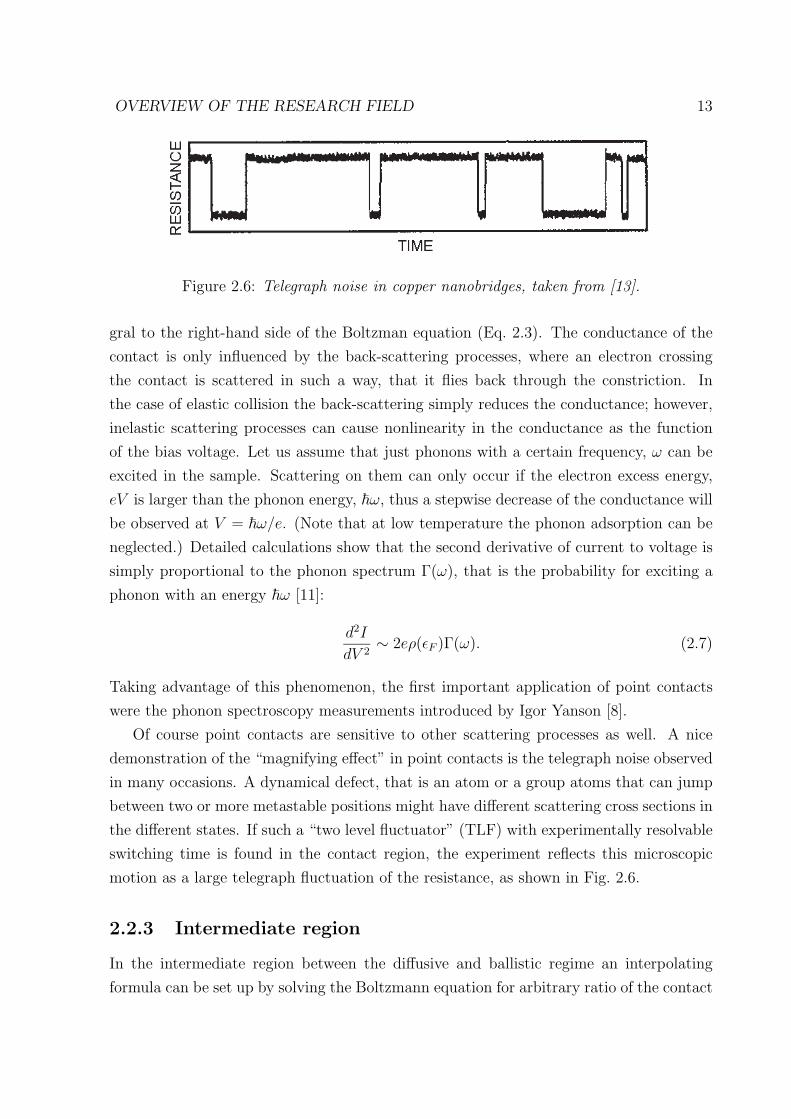
Figure 2.6: Telegraph noise in copper nanobridges, taken from [13].
gral to the right-hand side of the Boltzman equation (Eq. 2.3). The conductance of the
contact is only influenced by the back-scattering processes, where an electron crossing
the contact is scattered in such a way, that it flies back through the constriction. In
the case of elastic collision the back-scattering simply reduces the conductance; however,
inelastic scattering processes can cause nonlinearity in the conductance as the function
of the bias voltage. Let us assume that just phonons with a certain frequency, ω can be
excited in the sample. Scattering on them can only occur if the electron excess energy,
eV is larger than the phonon energy, ω, thus a stepwise decrease of the conductance will
be observed at V = ω/e. (Note that at low temperature the phonon adsorption can be
neglected.) Detailed calculations show that the second derivative of current to voltage is
simply proportional to the phonon spectrum Γ(ω), that is the probability for exciting a
phonon with an energy ω [11]:
d2I
dV 2∼ 2eρ(εF )Γ(ω). (2.7)
Taking advantage of this phenomenon, the first important application of point contacts
were the phonon spectroscopy measurements introduced by Igor Yanson [8].
Of course point contacts are sensitive to other scattering processes as well. A nice
demonstration of the “magnifying effect” in point contacts is the telegraph noise observed
in many occasions. A dynamical defect, that is an atom or a group atoms that can jump
between two or more metastable positions might have different scattering cross sections in
the different states. If such a “two level fluctuator” (TLF) with experimentally resolvable
switching time is found in the contact region, the experiment reflects this microscopic
motion as a large telegraph fluctuation of the resistance, as shown in Fig. 2.6.
2.2.3 Intermediate region
In the intermediate region between the diffusive and ballistic regime an interpolating
formula can be set up by solving the Boltzmann equation for arbitrary ratio of the contact

OVERVIEW OF THE RESEARCH FIELD 14
diameter and mean free path, l [14]:
R = l/d · 16
3πσd+ Γ(l/d)
1
σd, (2.8)
where Γ(l/d) is a numerically determinable monotonous function, Γ(0) = 1; Γ(∞) =
0.694. Note that the first term is exactly the Sharvin resistance by putting the Drude re-
sistivity into the formula, ρ = mvF /le2n, thus it is actually independent of l. This formula
provides the possibility to estimate the contact diameter from the contact resistance.
2.3 Ballistic transport in quantum wires
In the previous section a classical treatment of diffusive point contacts and a semiclassi-
cal approach to the ballistic limit was presented, where quantum mechanics only enters
through the Fermi distribution of the electrons. Now we shall go down to contact sizes
comparable to the Fermi wavelength, where coherent quantum phenomena play a funda-
mental role. A proper theory for the treatment of such quantum wires was introduced by
Rolf Landauer [15], which is briefly summarized bellow.
2.3.1 The Landauer formalism
First let us consider a single quantum wire, connecting two electron reservoirs with chem-
ical potentials µL = εF + eV/2 on the left-hand, and µR = εF − eV/2 on the right-hand
side (Fig. 2.7). Due to the quantum confinement, the transverse energies of the electrons
Reservoir+eV/2
Reservoir−eV/2
Figure 2.7: A quantum channel connecting two reservoirs.
are quantized (En), while the longitudinal plane wave motion is characterized by the wave
vector kn. This system is described by a set of one dimensional free electron dispersions,
just the bottom of each band is shifted by En:
ε(kn) = En +
2k2n
2m. (2.9)
Only the parabolas crossing the Fermi energy contribute to the conduction, which defines
the number of “conducting channels”, N . First we calculate the conductance of an ideal
OVERVIEW OF THE RESEARCH FIELD 15
quantum wire with a single conducting channel. The chemical potential for the right
moving and left moving electrons is shifted by eV , thus a current, I = evF ρ(εF )eV flows
through the wire. After inserting the one dimensional density of states, ρ(εF ) = (vF π)−1,
the conductance is G0 = 2e2/h = (12.9kΩ)−1, which is known as the quantum conductance
unit. It may look strange that an ideal wire without any scattering has finite resistance,
but it can be shown that this resistance arises from the interfaces between the reservoirs
and the wire. A four probe measurement, where the voltage drop is sensed on the wire
itself instead of the reservoirs reveals zero resistance [16].
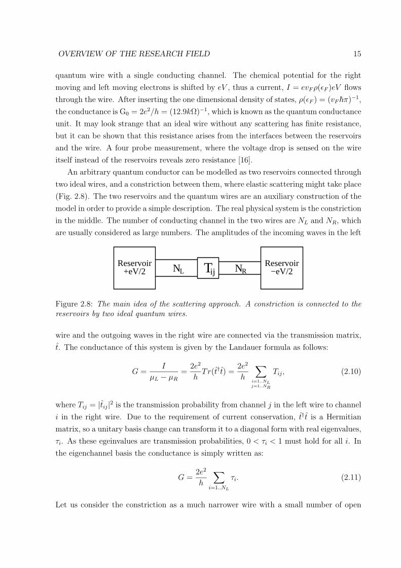
An arbitrary quantum conductor can be modelled as two reservoirs connected through
two ideal wires, and a constriction between them, where elastic scattering might take place
(Fig. 2.8). The two reservoirs and the quantum wires are an auxiliary construction of the
model in order to provide a simple description. The real physical system is the constriction
in the middle. The number of conducting channel in the two wires are NL and NR, which
are usually considered as large numbers. The amplitudes of the incoming waves in the left
Reservoir−eV/2
Reservoir+eV/2 TijNL NR
Figure 2.8: The main idea of the scattering approach. A constriction is connected to thereservoirs by two ideal quantum wires.
wire and the outgoing waves in the right wire are connected via the transmission matrix,
t. The conductance of this system is given by the Landauer formula as follows:
G =I
µL − µR
=2e2
hTr(t†t) =
2e2
h
∑i=1..NLj=1..NR
Tij, (2.10)
where Tij = |tij|2 is the transmission probability from channel j in the left wire to channel
i in the right wire. Due to the requirement of current conservation, t†t is a Hermitian
matrix, so a unitary basis change can transform it to a diagonal form with real eigenvalues,
τi. As these egeinvalues are transmission probabilities, 0 < τi < 1 must hold for all i. In
the eigenchannel basis the conductance is simply written as:
G =2e2
h
∑i=1..NL
τi. (2.11)
Let us consider the constriction as a much narrower wire with a small number of open

OVERVIEW OF THE RESEARCH FIELD 16
εF
T=1T=0
d(x)
En~(n/d(x))2
x
Figure 2.9: Lower panel: a quantum point contact with adiabatically changing width.Upper panel: the variation of the transverse energies along the quantum contact.
channels, Nc NL, NR. The number of open eigenchannels for the whole system is de-
termined by the narrowest cross section, and only Nc out of NL transmission probabilities
are nonzero in Eq. 2.11. Therefore, the Landauer formalism gives a simple description for
quantum constrictions, by characterizing them with a few transmission coefficients.
After presenting the simplicity of the formalism, we also have to mention the important
physical assumptions of the model. First of all the transport through the whole quantum
confined region is considered to be coherent, thus only elastic scatterings are allowed. This
also means that the irreversible ohmic dissipation associated with the finite conductance
of the system occurs via the thermalization of the electrons in the reservoirs. On the other
hand the emission or reflection from the reservoirs is always incoherent. Furthermore, in
each quantum wire the incoming modes are in thermal equilibrium with the connected
reservoir. The main limitation of the model is, that it cannot describe the dephasing
processes, which might be crucial under certain circumstances.
2.3.2 Conductance quantization
The Landauer formalism gives a simple description for ballistic quantum point contacts.
The bottom part of Fig. 2.9 shows a PC with adiabatically changing width, which means
that the contact diameter changes slowly compared to the Fermi wavelength. In this case
we can plot the transverse energies along the contact axis (top part of Fig. 2.9). Those
channels that are open even at the narrowest cross section of the wire are fully transmit-

OVERVIEW OF THE RESEARCH FIELD 17
Figure 2.10: Conductance quantization in two dimensional electron gas systems, takenfrom [18].
ting, and the rest are fully reflecting. Consequently the conductance of the contact is an
integer multiple of the conductance quantum, G0 = 2e2/h:
G =2e2
hNc, (2.12)
where Nc is the number of open channels in the contact center. This also means, that
the conductance changes in steps of G0 as the diameter of the contact is increased. Small
deviations are only expected just at the opening of a new channel, when one of the
transverse energies almost touches the Fermi energy. In this case the reflection in the new
channel is enhanced, but it rapidly vanishes during the further increase of the contact
diameter [17]. On the other hand any sharp irregularity in the channel wall can cause
significant reflection, which destroys the conductance quantization phenomenon.
Experimentally, conductance quantization was first observed in two dimensional elec-
tron gas (2DEG) systems [3, 4]. Due to the extremely large Fermi wavelength in 2DEG
devices (λF ≈ 40 nm) quantum point-contacts can be produced by means of electron
litography. The applied voltage on the gate electrodes above the 2DEG tunes the width
of the quantum channel between the two reservoirs (see Fig. 2.10a). The conductance
of the constriction as a function of the gate voltage clearly demonstrates the quantiza-
tion phenomenon (Fig. 2.10b). Recently it has been shown, that the transmission of a
certain channel can be reduced by placing a charged AFM tip above a maxima of the

OVERVIEW OF THE RESEARCH FIELD 18
(a) (b)
Figure 2.11: Conductance quantization in a three dimensional channel, taken from [19].
channel’s wave function at the entrance of the contact [18]. In this case the conductance
step corresponding to the opening of this certain channel is significantly smaller, while the
rest of the steps unaffectedly show a change of 1 G0. Of course conductance quantization
can only exist, when the energy splitting between the channels is much larger then the
temperature. In 2DEG systems this requires measurements in the subkelvin range.
The eigenmodes of a three dimensional quantum wire are given by the Bessel functions,
indexed by the quantum number m. Due to the cylindrical symmetry of the system, all
the m = 0 modes are two-fold degenerate, so there are some “double jumps” in the
conductance as the diameter of the wire is increased. Looking at the sequence of the
eigenmodes, it turns out, that the first four possible quantum conductance values are:
G = 1, 3, 5, 6 G0, (2.13)
and the G = 2, 4 G0 values are excluded. This is also demonstrated in Fig. 2.11b, showing
the calculations of J. A. Torres for hiperboloic quantum contacts with different opening
angles (Fig. 2.11a) [19]. At small opening angles the contact is a long quantum channel,
thus the conductance is quantized as given by Eq. 2.13 as diameter is increased. For large
opening angle we have an orifice-like contact, and the conductance is a smooth function
of the contact area with slight quantum oscillations. The intermediate region exhibits
smoothed plateaus at the quantized values.
These calculations have also shown that the conductance of an orifice-like quantum
point contact is not well described by the semiclassical Sharvin formula (Eq. 2.5). After
OVERVIEW OF THE RESEARCH FIELD 19
the inclusion of quantum corrections [19], the conductance is written as:
G =2e2
h
(kF d
4− 1
4
)2
. (2.14)
Three dimensional quantum wires can be established in metals. In this case, however,
the Fermi wavelength is comparable to the interatomic spacing, and the conductance
quantization might be destroyed due to the atomic roughness of the contact. This problem
is addressed in detail in the next section.
2.4 Atomic-sized conductors
In the recent years a great attention has been focused on the nature of conductance
through single atoms. Inserting atomic diameters into the formula 2.14 yields conduc-
tance values close to the quantum unit, G0. This imposes two main difficulties in the
observation of pure conductance quantization. First, as it was already mentioned, the
perfect transmission of the open channels might be reduced by the atomic-scale surface
corrugation. Furthermore, it is simply impossible to smoothly change the contact di-
ameter on this scale. On the other hand, if conductance quantization existed, it would
survive also at room temperatures due to the large energy splitting (≈ 1 eV) between the
modes. The above difficulties make it even more challenging to understand the interplay
between the atomic discreteness of the matter and the coherent quantum phenomena in
such nanojunctions. In this section we present the experimental tools that provide an
insight into the character of conductance channels in atomic-sized conductors.
There are several methods to establish atomic-sized contacts (see Sec. 2.1), but the
most of them are based on the same principle. If a contact of large size is pulled apart
by fine displacement of the electrodes, the neck in the middle is elongated, and thus the
contact diameter is decreasing. In the last stage of this process mostly a single atom
connects the electrodes, and thereafter the contact completely breaks and only tunnel
current can flow. In the experiments only the precise displacement of the electrodes is
adjusted (usually by changing the voltage on a piezo positioner), and the evolution of the
contact shape during the rupture remains unknown.
The change of the conductance during the break of gold nanocontacts is shown in
Fig. 2.12a. The figure demonstrates that each conductance trace is completely different
due to the uncontrollable nature of the breaking process. However, some common features
can be recognized: there are always certain plateaus, and between the plateaus there are
jumps with experimentally unresolvable sharpness. It is tempting to say that the magni-

OVERVIEW OF THE RESEARCH FIELD 20
0 50 100 150 200 250 3000
1
2
3
4
5
6
7
8
Gold
Con
duct
ance
(2e2 /h
)
Piezo-voltage (V)
(a) (b)
Figure 2.12: (a) – Conductance traces of breaking gold nanocontacts, taken from [20]. (b)– Conductance histogram of gold, taken from [21].
tude of the jumps is close to the conductance unit, but due to the irreproducibility proper
statistical analysis is required to justify this observation. One can repeat the breaking
process several times, and collect the measured conductance values into a histogram.
Naturally, the frequent occurrence of plateaus at a certain conductance value yields a
peak in the conductance histogram. Such a histogram for gold contacts is presented in
Fig. 2.12b, showing a sharp peak at 1 G0, and two smaller and broader peaks slightly
bellow 2 G0 and 3 G0. In spite of the “quantized” positions of the peaks, the conductance
traces in Fig. 2.12a cannot be described in terms of pure conductance quantization as it
was demonstrated by the simultaneous conductance and force measurements of Rubio et
al. [22] (Fig. 2.13). Along the conductance plateaus the force acting in the contact gently
increases, while the drastic jumps in the conductance are always correlated with sudden
force release. This means that the junction is elastically deformed along the plateaus, but
above a certain limit the atomic arrangement becomes unstable, and the contact jumps to
an other configuration. The conductance jumps are always due to atomic rearrangements,
in contrast to the smooth opening of a new channel in the 2DEG contacts. In spite of that
we cannot exclude, that the position of the plateaus is somehow governed by conductance
quantization.
Before going into more details, let us have a look at the conductance histogram for
other two metals. Fig. 2.14 shows the histograms for potassium and niobium contacts,
respectively. Concerning the other metals, Na and Li show similar histogram to potassium,
the noble metals have histograms like gold, and the rest of the metals usually resemble the
behavior of niobium, in the sense that only a single, broad peak is seen in the histogram.
The position of the peaks in the alkali metals (1,3,5 and 6 G0) is an undoubtable indication

OVERVIEW OF THE RESEARCH FIELD 21
Figure 2.13: Force measurements on gold nanocontacts, taken from [22].
for conductance quantization in a cylindrical wire (remember Eq. 2.13). It can argued
that in alkali metals the weakly bound s-electrons strongly reduce the atomic surface
corrugation, thus in the most of the breaks the contact is well approximated with a
free electron gas in a smooth channel with cylindrical symmetry. In the case of noble
metals, still with single s-electrons, there are signs of conductance quantization, but the
cylindrical symmetry is no longer indicated. In d and sp metals the electrons experience
a more rough channel due to the exotic shape of the atomic orbitals, which destroys
the conductance quantization. It is known from theoretical studies, that the number
of open channels in a single atom contact cannot be more than the number of valence
orbitals in the certain metal [23]. For instance in niobium with partially filled d-band,
five conductance channels are available, which are only partially open. Therefore, the
peak in the conductance histogram around 2.5 G0 can easily be the conductance through
a single Nb atom with channels halfly open in average. Indeed several theoretical and
experimental studies justify that the first, or in many occasions the only one peak in the
histogram presents the conductance of a single-atom contact [24]. This picture is also
supported by the following single argumentation. Assumably the last stage of the contact

OVERVIEW OF THE RESEARCH FIELD 22
(a) (b)
Figure 2.14: The conductance histogram of potassium (a) and niobium (b), taken from[24] and [25], respectively.
break is mostly similar: a single atom connects the electrodes. This arrangement yields
almost the same conductance values regardless of the exact arrangement of the whole
contact, so its statistical weight is enhanced in the conductance histogram.
2.4.1 Exploring the conductance eigenchannels of single atoms
We have seen that conductance measurements alone can already provide valuable infor-
mation about atomic-sized conductors. The conductance histograms show signs of con-
ductance quantization for s-metals, and generally they give the conductance of a single
atom contact. A further step would be the determination of the individual transmission
coefficients. The conductance eigenchannels in a monoatomic contact are connected to
the valence orbitals [23]; therefore, the experimental determination of the transmission
coefficient set would provide a deeper understanding of the nature of conductance through
a single atom. For this purpose, it is not enough to measure the conductance alone, which
is a sum of the transmission coefficients. In the following three possible procedures for
extracting more information about the individual transmission coefficients are discussed:
the measurement of shot noise or conductance fluctuations and the investigation of subgap
structure in superconducting junctions.
The shot noise is a fluctuation of the conductance arising due to the discreteness of the
electron charge. This means that an electron charge either fully goes through a barrier,
or does not go at all, and the detection of fractional charge transfer is not possible. The
probability for transmission is the transmission coefficient, τ itself, while the mean-square
deviation of this probability is τ(1 − τ). Translating it into the language of physics, a

OVERVIEW OF THE RESEARCH FIELD 23
1 2 3 40.0
0.1
0.2
0.3
5%
20%10%
x=0%
Exc
ess
nois
e(2
eI)
Conductance (2e2/h)
0 1 2 3 40.00.20.40.60.81.0
x
Tra
nsm
issi
on
Conductance (2e2/h)
Figure 2.15: Shot noise in gold nanocontacts, taken from [26]. The solid line shows thetheoretical prediction in the case of a single partially transmitted mode. The dashed curvescorrespond to the parallel opening of channels according to the illustration in the inset.The complete suppression of the shot noise at G = 1G0 shows that a single atom goldcontact has a single fully transmitting channel.
single channel conductor with conductance G = G0 · τ always exhibits a conductance
noise 〈∆G2〉 = G20 · τ(1− τ). This shows that the shot noise is fully suppressed at prefect
transmission or at perfect reflection. Taking advantage of this fact, one can for instance
judge whether the conductance through a single gold atom with G = 1 G0 is a perfect
transmission through a single channel, or partial transmissions through more channels.
The measurements support the first alternative (see Fig. 2.15); furthermore, it turns out
that in gold a new channel only starts to open if the previous channel are almost fully
open, which is called “saturation of channel transmission” [26].
The basic idea behind the conductance fluctuation measurements is represented on
Fig. 2.16a. An electron goes through the constriction with transmission τ , but it can be
partially reflected back by static impurities placed in the contact neighborhood. Upon
further reflection in the constriction with probability 1−τ , this wave can interfere with the
original one, causing a shift in the conductance. The fine details of this interference can be
tuned by changing the bias voltage, which sets the wavelength of the electrons. Therefore,
the conductance has an oscillatory pattern as a function of the bias voltage. Similarly
to the shot noise, this oscillation is suppressed for channels with full transmission or full

OVERVIEW OF THE RESEARCH FIELD 24
0.0
0.5
1.0
1.5
2.0a
σ
GV (
Go/V
)
0 1 2 3 40
10
20
G (2e2/h)
b
# p
oin
ts (
x 1
03 )
53000
(a) (b)
Figure 2.16: Conductance fluctuation in gold nanocontacts, taken from [28]. (a) – Theidea of quantum interference in a point contact. The transmission and the reflection ofthe contact is denoted by “t” and “r”, while “a” stands for the reflection in the diffusivebanks. (b) – The lower panel shows the conductance histogram of gold, while the upperpanel represents the magnitude of the conductance fluctuation at different conductancevalues averaged for a large amount of contacts.
reflection. The measurements on gold indeed show a strong suppression of the conductance
fluctuation at the quantized conductance values (Fig. 2.16b), which again supports the
idea of the saturation of channel transmission [27, 28].
The previous two methods were useful to judge whether one or more partially open
channels are present in the contact, but in the case of more channels they cannot provide
the individual transmission coefficients. A fundamental tool to determine all the trans-
mission eigenvalues is the measurement of subgap structure in superconducting point
contacts. In a traditional tunnel junction a quasiparticle can cross the barrier with prob-
ability τ if the voltage is more than two times larger than the superconducting gap,
eV > 2∆. Higher order processes are also possible due to the Andreev reflection, which
will not be discussed here in detail (for review see [7]). In an n-th order process, a charge
of ne can be transmitted through the barrier with probability τn, if eV > 2∆/n. In
tunneling experiments τ 1, and thus the higher order processes are heavily suppressed.
On the other hand in atomic point contacts τ is in the order of unity, so the above
phenomenon is experimentally resolvable as a special structure in the I − V curves at

OVERVIEW OF THE RESEARCH FIELD 25
Figure 2.17: Subgap structure in a superconducting aluminum nanocontact, taken from[29]. The dots represent the measured data, while the lines show the theoretical fits inwhich respectively one, two, and three conductance channels were included.
fractional values of the gap. A measurement for an aluminum contact is presented in
Fig. 2.17. It is clearly seen, that the inclusion of at least three eigenchannels is necessary
to get a proper theoretical fit. Both the number of channels and the value of transmission
coefficients is in good agreement with tight binding calculations [23]. These calculations
have shown that a single-atom aluminum contact has three conduction channels, one con-
nected to the combination of s and pz orbitals, and two connected to px and py orbitals.
The first channel has higher transmission, while the remaining two degenerated channels
are poorly conducting. The fourth channel expected from the number of valence orbitals
is completely closed. Note, that a single atom Al contact has a conductance less than one
quantum unit (G ≈ 0.8 G0), and still it has three open channels!
Similar measurements were done for contacts of the d-metal niobium, the p-metal lead,
and the s-metal gold. (The latter was driven superconducting by the proximity effect.)
The results of the measurements have shown, that a monoatomic Au contact has a single
channel with perfect transmission, Pb has three channels like aluminum, while Nb has
five channels. In the last two cases the channels are not perfectly transmitting.
2.4.2 Formation of atomic chains
The monoatomic gold contact has a conductance of 1 G0 due to the perfect transmission
through a single channel. Experimentally this contact is seen as the last plateau in the

OVERVIEW OF THE RESEARCH FIELD 26
0 4 8 12 16 20 24 28 32
0
1
2
3
4
5
6
7
8
Plateau length
Return distance
Con
duct
ance
(2e2 /h
)
Electrode displacement (Å)
0 4 8 12 16 20
5
10
15
20
25
Ret
urn
dist
ance
(Å
)
Plateau length (Å)
(a) (b)
Figure 2.18: (a) – Extremely long last plateau during the break of a gold nanocontact,taken from [30]. (b) – Histogram for the lengths of the last plateaus, taken from [32].
conductance curve during the disconnection of the junction. However, a large portion of
the conductance curves show an extremely long plateau at 1 G0: the conductance stays
at the conductance quantum along an electrode separation that is much longer than an
interatomic spacing (Fig. 2.18a). Figure 2.18b shows the distribution of the length of the
last plateau during a large amount of contact fractures. This plateau length histogram
exhibits peaks at equidistant positions, and the distance between the peaks is close to the
bulk interatomic spacing. This observation implies that chains of single atoms are formed
at the last stages of the break, which can have length up to seven atoms; furthermore, this
atomic chains also have a perfect transmission [30]. The same phenomenon was found in
platinum and iridium contacts, while in other metals the chain formation was not observed
[31].

Chapter 3
Experimental techniques
In the following chapters the results of my Ph.D studies are presented. An important
part of my work was the development of a point-contact measurement system in the low
temperature solid state physics laboratory of the Budapest University of Technology and
Economics. This work included the planning and building of a point contact sample
holder, and the establishment of the instrumental environment required for the different
types of point contact experiments. Therefore, the presentation of my results starts
with the detailed description of the new system, also including the introduction of the
various measurements that can be performed by the setup. The next chapters present the
experimental results, which were partly obtained in the point contact laboratory of the
University of Nijmegen, in parallel with the development of the new system in Budapest.
3.1 Principles of the MCBJ technique
The measurement system implements the idea of the mechanically controllable break
junction (MCBJ) technique, which was introduced by Muller and co-workers [33]. The
principle of this method is presented in Fig. 3.1. A small piece of a metallic wire is fixed
at two points on a flexible substrate, a so-called bending beam. Between the fixing points
the cross section of the wire is reduced by making a notch. The bending beam is fixed
at both ends to the sample holder. In the middle a vertically moveable axe is pushed to
the beam, which can be precisely positioned with a combination of a differential screw
mechanism and a piezo stack. As the beam is bent, the sample wire starts to elongate
between the fixing points, which results in the reduction of the cross section, and finally
the wire completely breaks. Thereafter the contact can be reestablished by reducing the
bending of the beam.
The main advantage of the MCBJ technique is the fact that the sample is broken
27

EXPERIMENTAL TECHNIQUES 28
Figure 3.1: Schematic drawing of the MCBJ technique
in-situ at liquid helium temperature in a cryogenic vacuum. Therefore, the electrode
surfaces are “fresh” and can be kept very clean over a long period of time, even for
reactive materials. In contrast the preparation of clean sample and tip surfaces in scanning
tunneling microscopes is a crucial problem. A further advantage of the break junction
technique is the robust mechanical stability of the system. The electrodes are rigidly fixed
to the substrate at a very close separation ( 0.5 mm), so the length of the free standing
parts is much shorter than in a typical STM setup. This makes the junction insensitive
to mechanical vibrations. The drift of the sample holder due to thermal expansion is
minimized by the low and stable temperature of the liquid helium bath. Furthermore,
due to the mechanical configuration of the bending beam, the vertical motion of the axe
pushing the beam causes only a highly reduced horizontal displacement of the electrodes.
This means that any noise in the position of the axe (due to vibration, thermal expansion
or voltage instability on the piezo element) has only a strongly reduced influence on the
junction. This aspect is discussed in detail in the following paragraphs.
The elastic bending of beams is widely discussed in handbooks of mechanics. A basic
aspect of the bending is the presence of a so-called neutral line in the beam, which is not
elongated during the deformation. In beams with rectangular cross section, the neutral

EXPERIMENTAL TECHNIQUES 29
Figure 3.2: Displacements of the electrodes in an MCBJ
line is exactly in the middle between the top and the bottom surface, as shown in Fig. 3.2.
Let us assume that the neutral line is described by a circle with radius r after bending,
as presented in the lower part of the figure. Using the notations shown in the figure, the
length of the beam is expressed as L = 2βr, while the distance between the fixing points
is d = 2αr. The bending is obtained after pushing the middle of the beam vertically by
z, which can be expressed as: z = r − r cos β rβ2/2. Using the previous equations, the
angle α is written as: α 4zd/L2. Our goal is to express the horizontal displacement
of the tip ends, x as a function of z. (At this point we assume that the two wires just
touch at z = 0.) The main displacement is caused by the fact that the wires are placed
in a distance of s above the neutral line, so they move apart in the horizontal direction
by x1 = 2s sin α. However the precise displacement is only obtained after considering two
other factors. After bending, the axes of the wires are no longer horizontal which causes a
displacement of d−d cos α. On the other hand, the two points of the neutral line beneath
the fixing points get closer by d − 2r sin α. The sum of these two factors is written as
x2 = 2r sin α−d cos α dα2/3. After eliminating the angles and the radius, the following

EXPERIMENTAL TECHNIQUES 30
equations are obtained:
x1 8ds
L2z (3.1)
x2 16d3
3L4z2. (3.2)
The length of the beam is fixed by the design of the sample holder. In our setup this
length is L = 24 mm. The distance between the fixing points is a matter of sample
preparation. Typically it is in the range of d 0.5 mm, however if proper care is taken
it can be reduced to 100µm. The distance between the sample and the neutral line is at
least the half of the thickness of the beam. The typical dimensions for s are 0.5−0.7 mm.
In practice the sample only breaks after a finite bending depending on the size of the
notch. During the measurements the bending is typically varied by ∆z < 1 µm around
z 0.5−3 mm. The quotient of the displacement ratios dx2/dz and dx1/dz is 4d2z/3L2s.
Provided that d, z and s are in the same order of magnitude while L is much larger, the
nonlinear term, x2 can be neglected. It also has to be noted that the wire does not break
exactly in the middle between the fixing points, as indicated in top part of Fig. 3.2. This
asymmetry, ε causes a vertical displacement between the wire ends, y = 2ε sin α which is
expressed as:
y 8εd
L2z. (3.3)
Naturally, this displacement is always smaller than x1 by a factor of ε/d, so it does not
give a dominant contribution to the displacement ratio. However it is better to avoid the
“sliding” motion of the electrodes by making the notch in the middle as much as possible.
Inserting the practical dimensions of the setup to the equations obtained, the reduction
ratio, dx/dz is in the range of 1 : 102 − 1 : 103. However, this simple calculation included
some assumptions that are not satisfied in reality. In practice the bending of the substrate
is not homogenous, and the main deformation takes place in the middle part. This
causes an effectively shorter length, L. The plastic elongation of the electrodes before
the break was also not included. This results in an effectively larger electrode length, d.
Therefore these simple considerations only give indications about the mechanical behavior
of the setup, and help to understand the importance of different lengths at the sample
preparation process. For precise calibration of electrode separation special measurements
are required, as described later in Sec. 3.4.1. These measurements revealed a typical
reduction ratio of 1 : 50.
Beside the important advantages of the MCBJ technique, like the cleanliness and the
stability, the main disadvantage also has to be noted. Due to the uncontrollable details of

EXPERIMENTAL TECHNIQUES 31
notch
stycast drop
electronicconnections
sample wire
bendingbeam
Figure 3.3: Photo of a sample prepared on the top of a bending beam. The upper panelshows an enlarged view of the notch in the middle of the sample wire.
the breaking process, the exact shape and orientation of the electrodes is always unknown.
This imposes serious difficulties in the interpretation of single measurements on a certain
contact, and in many cases a statistical approach is required.
3.2 Sample preparation
The photo of a typical sample is shown in Fig. 3.3. As a substrate phosphor-bronze plates
are used with dimensions of 24 × 10 × 0.4 mm or 24 × 10 × 0.6 mm. On the top of the
phosphor-bronze bending beam a thin (0.2 mm) insulating layer of kapton foil is glued
using a standard epoxy. This insulating layer protects against short circuits between the
sample and the sample holder.
The sample wire, which has a typical diameter of 100µm, is fixed on the top of the
bending beam by two drops of Stycast 2850 FT epoxy. Special care must be taken to
place the epoxy drops as close to each other as possible, and still to avoid their confluence.
Therefore, the sample preparation is done when the Stycast already starts hardening.
After the sample wire has been rigidly fixed on the substrate, a notch is established
between the fixing points. Usually the notch reduces the diameter by 70 − 90 %. The
preparation of the notch depends on the material of the sample. In soft metals the
notch is simply cut by a commercial blade under a microscope. For hard metals, either a
diamond-coated wire is used to “rasp” a notch, or electrochemical etching is applied.
Electrical contacts for biasing and sensing are made on the outer parts of the wires

EXPERIMENTAL TECHNIQUES 32
Figure 3.4: Modified sample mounting for a reduced displacement ratio. The sample isplaced on the top of two pads with typical dimensions of 6×2.5×1mm. The pads are madeof either fibre glass plates or shear piezo ceramics. In the case of shear piezo elements,the motion of the top plate is indicated by arrows.
(see Figs. 3.3) either by soldering or by using silver paint.
The discussion in the previous section implies, that the sample should be prepared
so that the largest possible displacement ratio is obtained, in order to have perfect sta-
bility. However, the maximum expansion of the piezo positioner is limited, thus if the
displacement ratio is too large, the contact size can be varied only in a restricted interval.
In certain measurements the contact size should be changed in a wide range, thus the
reduction ratio should be reduced on purpose. Still it is useful to minimize the length of
the free standing parts (d), and thus the distance of the sample from the bending beam
(s) should be increased. For this aim a thicker Stycast layer is placed below the sample,
or two fibre glass plates are glued between the sample and the beam (see Fig. 3.4).
One of the fibre glass plates can be replaced by a shear piezo element, which gives
a horizontal displacement of its surface if a voltage is applied. In this case the sample
is directly moved by the piezo without any reduction. (The typical displacement of the
shear piezo is 1 − 2 A for a voltage of 1 V.) The voltage contacts are connected to the
two layers of conducting epoxy (EPO-TEK H21D) which are fully covering the both sides
of the shear piezo plate. In this setup special care should be taken in order to avoid
any short circuit between the sample and the conducting epoxy on the top of the piezo.
Using small piezo plates, this setup still has an appropriate stability, and the combination
of the “main” piezo and the shear piezo is especially useful for collecting conductance
histograms, as it will be described in Sec. 3.4.2.
By applying shear piezos even a small STM can be built with the break junction. For
this purpose the left-hand side fibre glass plate is also replaced by a shear piezo, which
performs a displacement perpendicular to the axe of the contact (see Fig. 3.4). With this
setup the line profile of the electrodes can be traced. The displacement of the left-hand
side shear piezo is continuously varied, while a constant tunnel current is ensured by a
feedback circuit connected to the right hand side shear piezo. The feedback voltage gives
an indiction for the shape of the electrodes. It has to be mentioned, that this topography

EXPERIMENTAL TECHNIQUES 33
measurement with two “blunt” and irregular electrodes is rather qualitative. It can easily
happen that the role of the tip is changed between different parts of the electrodes during
the sweep.
3.3 The sample holder
A picture of the whole sample holder is presented in Fig. 3.5a. The sample is placed in the
bottom part (see Fig. 3.5c for an enlarged view), which is inserted into the liquid helium
bath during the experiments. This part is discussed in detail later on in this section.
The top part provides a room-temperature access to the system, including a valve for
the vacuum pot, electrical connectors, and a gear box driving an axe which goes down
to the the differential screw mechanism. The top and the bottom part is connected via
a stainless steel tube, which is soldered to the both parts. In the middle of it another
stainless steel tube is placed surrounding the stainless steel axe (see the illustration in
Fig. 3.5b). The smooth and concentric rotation of the axe is ensured by teflon rings fixed
to the axe. The wires for the electrical connections are running in the space between the
two stainless steel tubes. The inner part of the sample holder is a single vacuum space,
and all electrical and mechanical connections are tight for high vacuum. The building
blocks of the bottom and top part are mainly machined from brass.
The sample holder is fitted to the liquid helium cryostats by a standard NW50 flange
with O-ring seal. This flange is sliding on a third stainless steel tube, which is fixed
to the top part of the sample holder. This sliding seal enables the slow cool down of
the system. Furthermore measurements above the liquid helium temperature (4.2 K)
can also be performed by setting a proper distance between the sample and the liquid
helium surface. At such measurements, the temperature is precisely set by a temperature
controller driving a heating wire. The heating wire is rolled around the outer wall of
the vacuum coating in the bottom part. For temperature sensing a Cernox CX-1030-SD
thermometer is placed inside the vacuum pot, close to the sample.
The sample holder can be fitted to the two Oxford Instruments cryostats, or to the
two glass cryostats of the laboratory, and even to the liquid helium dewars (RH100). One
of the Oxford Instruments cryostats is equipped with a 14 T superconducting solenoid
magnet. As mentioned above, the temperature of the sample can be varied between
liquid helium and room temperature by lifting the insert. Temperatures below 4.2 K can
be obtained by pumping the Helium bath. This method provides temperatures down to
1.5 K. The Oxford cryostats are placed on large concrete blocks separated from the
building, which ensures the stable mechanical environment.

EXPERIMENTAL TECHNIQUES 34
Figure 3.5: (a) – Photo of the whole sample holder. (b) – Illustration of the stainless steeltubes and the axe going down to the bottom part. (c) – Enlarged view of the bottom partof the sample holder with removed vacuum coating.

EXPERIMENTAL TECHNIQUES 35
The design of the bottom part of the sample holder is demonstrated in Fig. 3.6. Panel
1 shows the whole setup in an assembled state. In panel 2 the vacuum pot is presented.
The ends of the two stainless steel tubes (2a and 2b) are fixed to the top plate of the
vacuum pot (2c). The vacuum coating (2d) is connected to the top plate by 8 screws.
The vacuum isolation is ensured by an indium wire placed in the slot 2e. The holes in
the top plate (2f) connect the vacuum spaces on the both sides, and give place for the
electrical wires to enter the vacuum pot.
The main axe with the differential screw mechanism and the piezo positioner is pre-
sented in panel 3. The outer part of the differential screw (3a) is fixed to the top plate
of the vacuum pot (2c) by screws. The middle part of the differential screw (3b) is fitted
to 3a with a thread M 8x0.5. On the inner part of the differential screw (3c) a thread
M 4x0.35 is cut, which fits into the inner thread of 3b. Due to the two small sticks (3d)
which are driven by the slots 3e, the inner part of the differential screw cannot turn. This
means that in one turn of the axe the middle part of the differential screw (3b) moves
downward by 0.5 mm compared to 3a, while 3c moves upward by 0.35 with respect to 3b.
Consequently the net vertical motion of 3c is only 0.15 mm. A 12 mm long piezo stack
(3f) is glued to the bottom of 3c with Stycast. On the other end of the piezo stack a small
“cap” is glued (3g), which pushes the bending beam. The differential screw is turned by
the axe (3h) coming from the top of the sample holder. The connection is established with
a “loose” fork-blade mechanism (3i). If the axe is turned slightly backward after setting
the appropriate position of the differential screw, the parts 3b and 3h have no contact at
all, so the differential screw is completely decoupled from any unwanted motion of the
long axe. The end of the axe is centered to the inner stainless steel tube (2b) by a teflon
ring (3j).
Panel 4 shows the body of the sample holder (4a) which is fixed to 3a by screws. The
outer wall of the body has the same diameter as the inner wall of the vacuum coating
(2d) in order to have good thermal contact with the cryostat. The bending beam (4b)
is inserted into the two slots in the body. The third part (4c) is a so-called back-spring.
The bottom plate of the back-spring is screwed to tho bottom of 4a. The top part of the
back-spring pushes the middle of the bending beam backward. This increases the rigidity
of the setup, and ensures that the beam can be bent back even if the elastic limit has
been exceeded. The spring itself is made of a phosphor-bronze wire.
The bending of the beam is roughly adjusted by rotating the axe by manually turning
a disc on the top of the sample holder. This course adjustment is only used if large
displacements are required, typically at the first break of the sample. For more precise
control the axe can be coupled to a worm-wheel gearbox with a 1 : 50 attenuation.

EXPERIMENTAL TECHNIQUES 36
12
34
2a 2b 2
c
2d
2f
2e
3b
3h 3j
3i
3a
3e
3c 3d
3f 3
g
4a
4b
4c
Figure 3.6: Assembly of the bottom part of the sample holder

EXPERIMENTAL TECHNIQUES 37
This means that in one turn of the worm of the gearbox, the differential screw moves
only 3 µm. The differential screw has a large hysteresis due to the several mechanical
couplings between the different parts. Furthermore due to the long axe and the friction
its motion is not necessarily continuous. Therefore, the piezo stack is used for the fine and
well-controlled adjustment of the bending. At room temperature the piezo stack exhibits
an elongation of 15 nm if a voltage of 1 V is applied on it. At cryogenic temperatures the
elongation is reduced by approximately 35 %. In order to avoid discharges, the voltage
range is limited to 0 − 300 V. A crucial aspect of the design is to have an appropriate
overlap between the whole range of the piezo and the resolution of the differential screw.
3.4 The way of the measurements
After the sample has been prepared as explained in Sec. 3.2, the following routine arrange-
ments are carried out before starting the measurements. The bending beam is placed into
the sample holder paying attention on not breaking the sample. For this purpose the
differential screw is set in such a position that the cap on the piezo element just touches
the bending beam. In this case the beam cannot be bent when the back-spring is in-
stalled. After that the electrical wires are connected, and the vacuum pot is closed. Then
the vacuum pot is pumped by a turbomolecular pump for a few hours. Because of the
long, narrow tubes it is hard to establish a vacuum better than 10−5 mbar in the bottom
of the sample holder. The high vacuum is ensured by the cryopumping effect after the
vacuum pot is inserted into the liquid helium bath. Due to the freezing out of all gases at
cryogenic temperatures, a typical vacuum of 10−10 mbar can be obtained. Therefore,
the reason for pre-pumping the insert for hours is rather to ensure the absence of leaks
on the vacuum coating. Especially the leaking of the indium sealing has to be checked,
which is replaced before every measurement. For precise determination of the leaking
rate, occasionally a helium sensitive leak detector is used. After the pumping has been
finished, the bottom of the sample holder is pre-cooled in liquid nitrogen, and finally
the insert is placed into the liquid helium cryostat. Using the sliding seal, the sample is
pushed slowly towards the helium surface, in order to avoid the boil-off of a large amount
of helium. When the insert has completely cooled down the sample can already be broken
as the cryopump guaranties a clean environment. This initial break is done by directly
turning the axe from the top. After that the relaxation of the whole setup for a few hours
is recommended. Finally a proper contact size can be set by adjusting the differential
screw via the gear box, and fine tuning the junction by the piezo element.
Depending on the particular type of measurement, different experimental conditions

EXPERIMENTAL TECHNIQUES 38
might be required. As mentioned in the previous section, the temperature of the insert
can be varied above 4.2 K by lifting the sample holder using the sliding seal. It is to
be noted, that at elevated temperatures the setup is loosing both from the mechanical
stability and the cleanliness of the environment. At T ≈ 14 K and T ≈ 54 K the cryopump
becomes ineffective against hydrogen, and oxygen respectively. In these cases the vacuum
can be improved by using sorption pumps in the sample space.
It also has to be mentioned that the heat conductance between metal surfaces is very
poor at cryogenic temperatures. In spite of the precise mechanical contacts between
the parts of the sample holder, the sample cannot cool down exactly to liquid helium
temperature. (The typical bottom temperature is T 8 K.) If the extremely stable
thermal environment is more important than the high vacuum, then helium exchange gas
is inserted into the vacuum space. In this case two crucial points must be kept in mind.
The vacuum spaces have a dielectric instability in the pressure range 0.01 − 10 mbar. In
this pressure range the high voltage applied on the piezo element might cause discharges.
Furthermore due to the presence of helium exchange gas the calibration procedure of the
electrode displacement (see Sec. 3.4.1) becomes inaccurate.
The details of the various measurements that can be performed by the setup are
discussed in the following subsections.
3.4.1 Conductance traces and the calibration of the electrode
separation
A basic application of the MCBJ setup is the measurement of the conductance as a
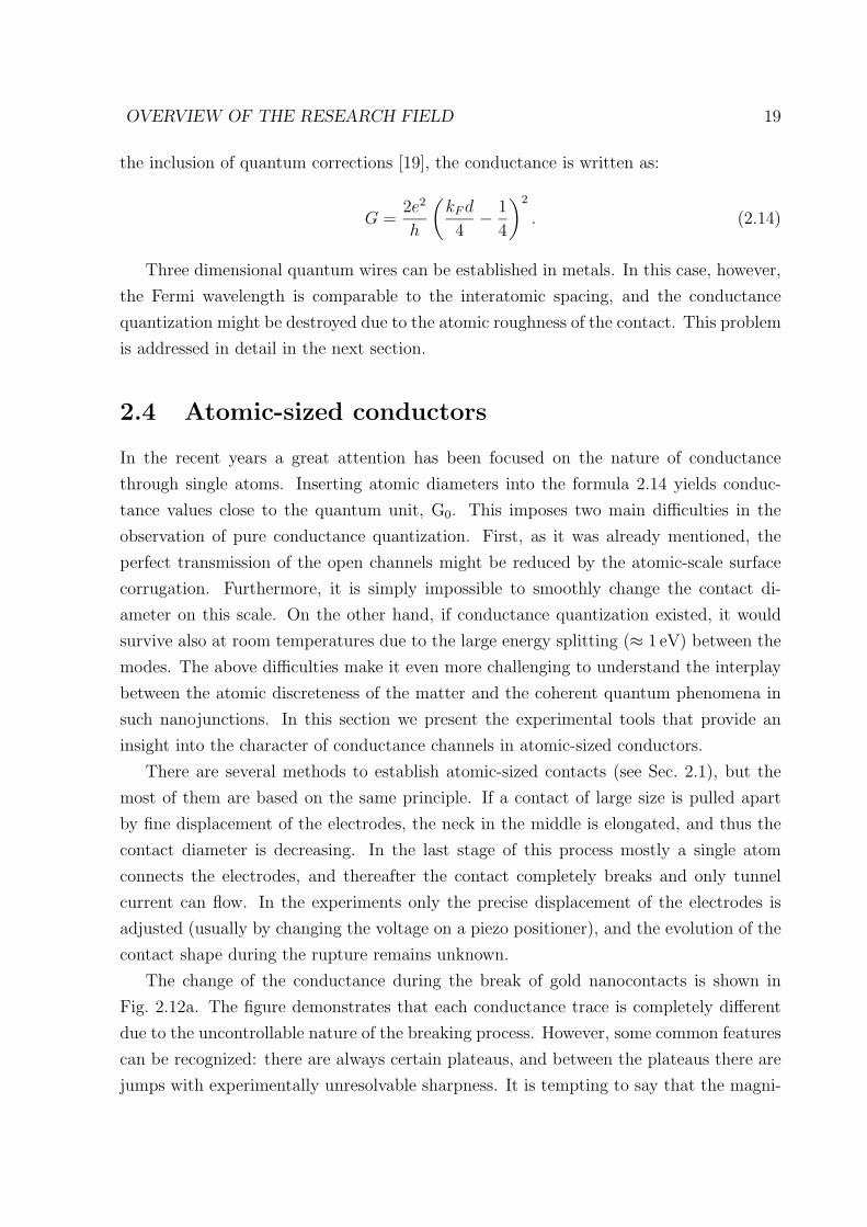
function of electrode separation. A typical curve is demonstrated in Fig. 3.7. In the initial
state the electrodes are completely disconnected, and only tunnel current is detected. As
the electrodes are pushed slowly towards each other the tunnel current is exponentially
increasing. At a certain point the adhesive forces between the electrodes become so
large that a sudden jump to direct contact occurs. Upon further electrode approach, the
contact size – and accordingly the conductance – increases through a series of atomic
rearrangements.
The separation of the electrodes is tuned by changing the voltage bias on the piezo
element. For this purpose a KEPCO ATE 325-0.8 DM high voltage amplifier is used,
which is controlled by a computer program. The analog control input of the amplifier
is connected to the analog output of a National Instruments PCI-MIO-16XE-10 data
acquisition board (with a resolution of 16 bit). The conductance is usually measured in a
voltage biased two-probe setup. Mostly both the voltage biasing and the current sensing
EXPERIMENTAL TECHNIQUES 39
-200 -150 -100 -50 0 50 100 150 2001E-6
1E-5
1E-4
1E-3
0.01
0.1
1
10
100
1000
metallic contact
jump to contact
tunneling regimeCo
nd
uct
an
ce (
2e2 /h
)
Piezo voltage (V)
Figure 3.7: Conductance trace for a Pb contact. The measurement covers a change ofnine orders of magnitude in the conductance.
can be done by a Keithley 2400 SourceMeter alone. At very large tunneling resistances
(> 1 GΩ) the resolution of the SourceMeter is not sufficient, and a Keithley 428 Current
Amplifier is used for measuring the current. By changing the range of the current sensing,
the conductance of the junction can be monitored over several orders of magnitude from
the far tunneling regime (≈ 100 GΩ) to low-ohmic contacts (≈ 10 Ω).
In this arrangement the measured resistance also includes the resistance of the cables
going down to the sample holder, and the contacts between the cables and the sample.
In a typical case this makes an error in the order of 1 Ω. The resistance of atomic-sized
conductors is in the range of the quantum unit, 1/G0 12.9 kΩ, thus the two-probe
measurement is sufficiently precise. If contacts of larger size are investigated, a current
biased four-probe arrangement can be applied to eliminate the cable resistances.
An important application of the above measurements is the calibration of the electrode
separation in the break junction. The conductance through a tunnel junction can be
written as:
G = Ce−√
8mφ
x, (3.4)

EXPERIMENTAL TECHNIQUES 40
40 41 42 43 44 45 46 471E-8
1E-7
1E-6
1E-5
1E-4
1E-3
0.01
0.1
1
10
0 120 240 360 480 600
-1
0
1
1Å
Jump to contact
Con
duct
ance
(2e
2 /h)
Piezo voltage (V)
Long term stability
Dis
plac
emen
t (p
m)
Time (s)
Figure 3.8: Calibration of the electrode separation using the tunneling part of the conduc-tance traces. The dotted line shows the linear fit, which gives a slope of ∂(log(G))/∂Vp =1.03 1/V. This corresponds to an electrode separation of 1.03 A upon unit change of thepiezo voltage. The deviation from the exponential behavior at very large resistances is dueto instrumental offset currents. The inset shows the drifting displacement of the electrodesas a function of time at constant piezo voltage.
where C is a coefficient depending on the junction geometry, Φ is the work function of
the electrodes, m is the electron mass, and x is the separation of the electrode surfaces.
Using a typical work function value of 5.1 eV for gold, it turns out that a change of an
order of a magnitude in G corresponds to an electrode displacement of 1 A. This simple
relation is used to determine the electrode displacement caused by unit voltage change
on the piezo element. A typical calibration curve is demonstrated in Fig. 3.8. The tunnel
conductance can be precisely measured over 5 orders of magnitude, showing a perfect
exponential behavior. Deduced from the slope of the curve, the electrode separation is
1.03 A/V in this particular case.
The mechanical stability of the system can be determined by measuring the electrode
separation as a function of time, at constant piezo voltage. The inset in Fig. 3.8 demon-
strates that the drift of the electrode separation during 10 minutes is less than 2 pm.
In the presence of He exchange gas the tunneling curves exhibit a strong deviation
from the exponential behavior [34, 35], so the above procedure cannot provide an accurate

EXPERIMENTAL TECHNIQUES 41
0
Co
nd
ucta
nce
(G0)
Figure 3.9: Panel (a) shows a single conductance trace during the break of a gold nanocon-tact. Panel (b) presents a histogram for the occurrence of different conductance values onpanel (a). Panel (c) is a summed histogram for 10000 independent contact fractures.
calibration. As an alternative, the electrode separation can be determined by measuring
field emission resonance spectra [36].
3.4.2 Building conductance histograms
In contrast to the precisely reproducible tunneling curves, the conductance of a direct
metallic contact is a poorly reproducible function of the electrode separation. The evolu-
tion of the junction is determined by complicated atomic rearrangements in the contact,
and every single conductance trace has a completely different shape. From this reason
the technique of conductance histograms was introduced to provide statistical informa-
tion about the irreproducible contact fracture. Fig. 3.9a shows a single conductance trace
recorded during the break of a gold contact. The histogram on panel (b) shows the oc-
currence of different conductance values along the conductance curve. Naturally, at the
place of conductance plateaus peaks in the histogram arise. After collecting thousands
of conductance traces and summing the corresponding histograms, the conductance his-
togram in panel (c) is obtained. The peaks in this histogram correspond to the statistically
preferred conductance values during the fracture.
In our setup conductance histograms are recorded in the following way. The repeated
fracture of the contact is established by applying a ramp voltage on the piezo element
with a typical frequency of 5 − 50 Hz (see the demonstration in Fig. 3.9). This ramp is

EXPERIMENTAL TECHNIQUES 42
generated by programming the analog output of the National Instruments data acquisition
board, which is driving the high voltage amplifier. A constant voltage is applied on the
contact, and the current is measured with the Keithley 428 Current Amplifier in a fast
mode (10 µs rise time). The output voltage of the current amplifier is accumulated by
the analog input of the National Instruments data acquisition board with a resolution
of 16 bit and a sampling rate of 20 − 100 ksample/s. The measured data are processed
on-line with a computer program, that is the “growth” of the histogram is visible on the
screen during the measurement. It should be noted, that in this arrangement – due to
the fast sampling rate – the resolution of the measured conductance is not as good as
in the measurements discussed in the previous subsection. Furthermore the change of
the current range is slow, thus it is avoided in this type of measurement. Consequently,
with the histograms only a restricted interval of the junction conductance is investigated,
usually the attention is focused on contacts with a few atoms in the cross section.
The amplitude and the offset of the ramp voltage is used to tune the indentation
of the contact, that is the maximal junction size established in each cycle. Typically
these parameters have to be set so that in every period the electrodes are pushed to reach
Gmax 30 G0, and thereafter they are pulled until the complete break. Traces that do not
reach the tunneling regime should be excluded, as they might not include the last stage of
the break corresponding to a single atom contact. At small indentations (Gmax 10 G0)
the conductance traces have a tendency for showing reproducible structures. In this
case the histogram might exhibit features corresponding to precisely repeating atomic
rearrangements instead of a statistical average, which should be by all means avoided.
The magnitude of the appropriate indentation is material dependent, for instance gold
junctions with Gmax = 10 G0 already break in a large variety of ways, while tungsten
contacts with Gmax = 30 G0 might still follow repeated traces. On the other hand too
large indentations should also be avoided. The drastic variation of contact size gives rise to
transient relaxation processes, which decrease the stability of the junction. (This aspect
has a particular importance if plateau length histograms are collected, which requires
perfect stability.) Furthermore, the large currents flowing at large contact sizes can cause
errors in the electrical circuits.
The computer program controlling the measurement monitors the conductance curves,
ensuring that just “good” traces are recorded. During the measurement some slow me-
chanical drifts might occur in the setup. This is compensated by a feedback routine,
which automatically tunes the offset of the ramp voltage.
As mentioned in Sec. 3.2 about the sample preparation, occasionally a shear piezo
plate is placed between the sample and the bending beam. In this case the ramp voltage
EXPERIMENTAL TECHNIQUES 43
is applied on the shear piezo directly from a function generator. This means that the
modulation of the electrode separation is not limited by the slow rise times of the high
voltage amplifiers and the slow mechanical response of the MCBJ setup. The rate of
indentation is adjusted by changing the deflection of the bending beam with the main
piezo element.
Beside the conductance histograms some additional statistical information can also
be extracted from the conductance traces. The search for certain correlations in the
data sets can provide valuable information about the system under study, as discussed in
the following chapters. These analysis can also be done on-line during the measurement.
However in most of the cases it is hard to find the best way of data processing beforehand,
and the huge amount of conductance traces is preserved for later evaluation.
3.4.3 Recording I-V curves
Another basic application of the MCBJ setup is the investigation of nonlinear features in
the conductance of the junction. Several physical phenomena can cause nonlinearity in
the I −V curves of nanojunctions. The characteristic voltage range of these features also
scatters over a wide interval, from the submillivolt range in superconducting tunneling
spectra, up to tens of volts in field emission resonance measurements [34]. A detailed
discussion of the nonlinear conductance of atomic-sized conductors is given in Chap. 6.
In this passage the experimental methods for recording I − V curves are discussed, and
some additional applications of the setup are demonstrated by introducing those types of
experiments that are not discussed elsewhere in this thesis.
The basic tool for recording I−V curves is the Keithley 2400 SourceMeter. This device
can bias voltages from 5µV up to 300 V and measure currents down to 10 pA. It can also
work as current source and voltage meter in a four-probe current biased measurement.
The sweep of bias voltage is controlled by a computer subroutine. This is integrated into
the program that records the conductance traces, so the user can select the appropriate
point of the conductance trace, where the I − V curve should be measured.
This arrangement has a perfect resolution: nonlinearities of 0.01 % can be detected
in the conductance of atomic-sized conductors. On the other hand, the recording of an
I − V curve requires a long time (30 − 300 s). During this time some mechanical drifts
in the junction might occur if the stability of the contact is not appropriate. Therefore,
the recording of the I − V curve is always repeated, and just the precisely reproducing
curves are accepted as real ones.
These slow drifts can be eliminated by performing faster measurements. For this pur-
pose the sample is biased by a triangle signal from a function generator, and the response

EXPERIMENTAL TECHNIQUES 44
-3 -2 -1 0 1 2 30
1
2
3
4
-3 -2 -1 0 1 2 3-4
-2
0
2
4
400µV
4∆/e
dI/dV (Μ
Ω−1)
Vbias
(mV)
I (nA
)
Vbias
(mV)
Figure 3.10: Panel (a) shows the I − V curve of a superconducting Pb tunnel junctionrecorded by a digital oscilloscope. In panel (b) the numerical derivative of the I −V curveis presented.
of the contact is measured by an oscilloscope. (In our setup a LeCroy 500MHz digital
sampling oscilloscope is used.) The resolution of such measurements is typically 1 %.
This method was tested by measuring the superconducting gap of Pb tunnel junctions.
The recorded I − V curve is presented in Fig. 3.10a, followed by the differential conduc-
tance curve on panel (b) obtained after numerical differentiation. The half-width of the
two peaks on panel (b) demonstrate, that the voltage smearing of the setup is 400µV,
which is already comparable to the temperature smearing at 4.2 K. Here it must be noted,
that in the sub-millivolt range a considerable smearing of the curves might result from the
high-frequency voltage pick-ups on the cables. In order to eliminate these disturbances
proper RC filters should be applied both at the top and at the bottom of the sample
holder.
In most of the experiments the first or even the second derivative of the I − V curve
reflects the basic physical information about the system. If the resolution of the I − V
curve is appropriate, there is always a possibility for numerical differentiation. However,
the derivative curves can be directly measured by applying Lock-In techniques. In this
case the DC bias voltage is modulated by a sine signal. The first or the second harmonic

EXPERIMENTAL TECHNIQUES 45
-40 -20 0 20 403.910
3.915
3.920
3.925
dV/d
I (Ω
)
Bias voltage (mV)
Figure 3.11: The differential resistance of a Ni59Nb41 metallic glass point contact. Theanomalous feature around zero bias is attributed to scattering on two level systems.
response of the sample – which is indeed respectively the first or second derivative of the
I − V curve – is detected by a Lock-In amplifier. An example for such a measurement is
presented in Fig. 3.11. The differential resistance of a mesoscopic metallic glass contact
shows an anomalous behavior around zero bias due to the scattering on two level systems
[37].

Chapter 4
Transition from direct contact to
tunneling in tungsten
In this chapter experiments on tungsten nanojunctions are presented. These studies were
aimed at examining the influence of the extraordinary mechanical and electronic properties
of tungsten on the transition between tunneling and direct contact. The measurements
have shown, that in tungsten the adhesive jumps are occasionally absent, so the junction
can be investigated at ultra-small electrode separations. By employing the conductance
histogram technique the preferential values of conductance during the fracture of the
junction have been determined.
4.1 Introduction
As it has been discussed in the introductory part of the thesis (Sec. 2.4), the transport
properties of breaking metallic nanocontacts are governed by two basic phenomena. The
conductance of a certain atomic configuration is determined by the transmission coeffi-
cients of the open conductance channels, which are mainly related to atomic orbitals. The
process of contact breaking is controlled by nanomechanics: the elastic and plastic defor-
mation of matter on atomic scale. The majority of the metals exhibit similar behavior
during the contact fracture. As the electrodes are separated, a neck is pulled in the mid-
dle, which becomes narrower and narrower through a series of atomic rearrangements.
Finally the junction completely breaks, and thereafter the vacuum tunneling gives the
conduction of the constriction. The conductance of the junction decreases in steps due
to the atomic rearrangements, followed by an exponential decay in the tunneling regime.
The break happens in a rather uncontrollable and irreproducible way, however the very
last stage is mostly similar: a single atom forms the contact. In the majority of the metals
46

TRANSITION FROM DIRECT CONTACT TO TUNNELING IN TUNGSTEN 47
0 1 2 31E-3
0.01
0.1
1
tunneling regime
single atom contact
jum
p to
cont
act
disruption
cond
ucta
nce
[2e2 /h
]
electrode displacement [Å]
Figure 4.1: Transition between direct contact and tunneling regime in a gold junction. Thefigure demonstrates the jump-like rupture of a monoatomic contact during the retractionof the electrodes, and the jump to single atom contact as the electrodes are subsequentlyapproached. A hysteresis is observed between the two transitions.
the conductance histograms do not show any special feature, except for a smeared peak
at the conductance through a single atom.
In this study special attention is focused on the transition between the tunneling
regime and direct metallic contact. This transition usually occurs as a spontaneous jump
instead of a smooth evolution [38]. During the approach of the electrodes from large
separation, initially the exponential tails of the wave functions overlap giving rise to
tunneling through the vacuum barrier. As the electrode separation becomes comparable
to the lattice constant a significant overlap is established, which results in an attractive
adhesive force. The system can lower its surface energy by jumping into contact, but
it requires elastic or even plastic deformation of the junction. Therefore, the occurrence
of this spontaneous jump is controlled by the competition between the adhesive and
tensile forces. Similar physics governs the disconnection of the junction: the system
does not like to loose surface energy, so the contact breaks in a jump-like way after a
considerable overstretching of the junction. It is not enough to compare the energies
of the “unstretched, broken” and the “stretched, connected” configurations, as there is
TRANSITION FROM DIRECT CONTACT TO TUNNELING IN TUNGSTEN 48
a potential barrier between these two metastable states [39]. Indeed, a hysteresis is
observed between the disconnection and the jump to contact, as demonstrated in Fig. 4.1.
This spontaneous jump has precluded the measurements of conductance at sub-Angstrom
distances between the electrodes for all metals studied to date.
The measurements of thermal expansion of MCBJ electrodes for different materials
have pointed out the unusually high stability of tungsten tunnel junctions at very close
electrode separations [40]. In another study, transmission and scanning electron mi-
croscopy images showed no evidence of connective neck formation between tungsten wires
[41]. Moreover, measurements of adhesive forces between an atomically-defined W(111)
trimer tip and a Au(111) sample revealed no spontaneous jump to contact [42]. These
unusual properties of W gave motivation to perform extensive conductance measurements
on tungsten nanojunctions.
4.2 Experimental details
In the measurements high purity (99.999 %) polycrystalline tungsten wires with a diameter
of 100 µm were used. The modified sample mounting presented in Fig. 3.4 in Sec. 3.2 was
applied, that is the sample was fixed on the top of two small pads. The central section of
the wire was electrochemically etched in a 25% solution of KOH down to 5–10 µm at its
thinnest part. In each measurement, the right-hand side pad was a shear piezo element,
which was used for modulating the electrode separation.
In certain cases STM-like line-profile measurements were performed (as described in
Sec. 3.2) by placing the sample on the top of two shear piezo elements with perpendicular
displacements. These studies have shown, that the electrodes have atomically flat parts
up to 5–10 nm in length alternating with irregularities of 5–15 A in height. It should
be noted that these topography measurements with two “blunt” electrodes are rather
qualitative and the numbers presented are only rough estimates.
4.3 The nature of conductance traces in tungsten
contacts
The transition from the tunneling regime to direct contact in tungsten MCBJ was studied
in detail by recording conductance traces (as described in Sec. 3.4.1) during slow, con-
tinuous approach or retraction of the electrodes. While in the majority of metals all the
traces follow a similar pattern, the measurements on tungsten revealed a rich variety of

TRANSITION FROM DIRECT CONTACT TO TUNNELING IN TUNGSTEN 49
0 1 2 3 4 6 7 81E-4
1E-3
0.01
0.1
1
10
100
21cond
ucta
nce
[2e2 /h
]
distance [nm]
240
280
0 1 2 3 4
Figure 4.2: Two extreme cases of conductance traces for W MCBJ. 1 – avalanche-liketransition from tunneling to a low-ohmic contact. The upper panel shows the conduc-tance in the process of retraction. 2 – transition from tunneling to direct contact withoutspontaneous formation of an adhesive neck.
conductance curves. The two extreme cases are shown in Fig. 4.2. Curve 1 demonstrates
an avalanche-like transition from G ≈ 0.01 − 0.1 G0 to 100 − 1000 G0. This indicates
the formation of a mesoscopic contact with a cross-section of 10–100 nm2. Subsequent
retraction of the electrodes produced only small changes in the conductance over a re-
treat distance of 4 nm, which were followed by sudden disconnection (upper panel in
Fig. 4.2). The other extreme case – curve 2 in Fig. 4.2 – demonstrates a smooth transition
from tunneling to direct contact with no sign of spontaneous formation of an adhesive
neck. However, the majority of the conductance curves exhibited a combination of smooth
changes and sudden jumps with amplitudes ranging from 0.1 G0 up to few G0.
To investigate the rich variety of conductance curves, a statistical analysis was per-
formed using the conductance histogram technique (as described in Sec. 3.4.2). It was
found that tungsten nanojunctions have a particular tendency to show reproducible, al-
most identical conductance traces when the indentation of the electrodes is not sufficiently
large. A statistical approach to data analysis is only justified if the irreproducibility of
successive traces is properly checked. Usually, if contacts of Gmax 30–40 G0 are formed
in every cycle, the break already occurs in a large variety of ways. However, in some cases
the conductance traces repeatedly showed an avalanche-like jump to low ohmic contact
(like curve 1 in Fig. 4.2), which prevented the measurement of conductance histograms.
We also found, that the occurrence of these avalanche-like transitions is more probable if

TRANSITION FROM DIRECT CONTACT TO TUNNELING IN TUNGSTEN 50
a
1 2 3 4 5
b
conductance [2e2/h]
cou
nts
[a
rb. u
nits
]
1 2 3
1 2 3
Figure 4.3: Conductance histograms for W MCBJ based on 10000 conductance traces.Upper panel – featureless histogram. Lower panel – histogram with peaks around 1 and2G0. Insets: histograms for the traces with the most pronounced plateaus selected fromthe corresponding data set. The selections include 10% and 20% of all curves in panel(a) and (b), respectively.
already a large amount of conductance traces were recorded on a certain junction, which
indicates the flattening of the electrodes during the measurement. In these cases the junc-
tion had to be changed by replacing the sample or by shifting the contact-site with the
left-hand side shear piezo (see Fig. 3.4). The shape of those traces that were appropriate
for measuring conductance histograms was also sensitive to the selected contact-site, and
the histograms recorded on different junctions did not necessarily exhibit the same pat-
tern. These features are in sharp contrast to the majority of metals, where all junctions
are appropriate for conductance histogram measurements, and the replacement of the
junction cannot cause significant changes in the statistics.
Due to the sensitivity on the selected junction site, the characteristic behavior of tung-
sten nanocontacts could only be extracted from a large amount of histograms, recorded
on different junctions. It was found that the conductance histograms can be divided
into two basic categories. A major part of them demonstrated no distinctive features,
as demonstrated in Fig. 4.3(a). However, on many occasions the histograms showed two
peaks at respectively 1–1.2 and 2–2.2 G0 (Fig. 4.3b), or only one of those two peaks.

TRANSITION FROM DIRECT CONTACT TO TUNNELING IN TUNGSTEN 51
0.0 0.2 0.4
1
2
3
4
5
6
distance (nm)
3b3a21
cond
ucta
nce
[2e2 /h
]
Figure 4.4: Typical conductance traces for W. Curve 1 – featureless curve. Curve 2 –smooth transition to tunneling with distinct plateaus. Curves 3a and 3b – traces withsudden jumps of conductance.
Each histogram was based on 10000 individual conductance curves. As a demonstra-
tion, four characteristic traces were extracted from the data sets (Fig. 4.4). Curve 1 shows
a smooth and completely featureless transition from direct contact to tunneling. Curve
2 is a similarly smooth transition with distinct plateaus at 1 and 2 G0. Curves 3a and
3b show clear conductance jumps. It must be mentioned, that the last two curves have a
customary shape which could be observed in many metals. The jump-like rearrangement
of the contact is preceded by a certain overstretching of a stable atomic configuration, re-
flected as a pronounced conductance plateau. As a sharp contrast, the completely smooth
traces with or without distinct plateaus (curves 2 and 1, respectively) were not observed
in other metallic contacts to date.
In order to determine the contribution of the different types of conductance curves to
the histogram we have developed computer algorithms for characterizing the individual
traces. This analysis concentrated on two basic aspects: the smoothness of the trace and
the existence of plateaus. The smoothness of the curve was characterized by the largest
conductance jump between the neighboring data points in the interval G/G0 ∈ [0.3, 3.3].
If this maximal jump is comparable to the average difference between successive data
points, the trace is regarded as a smooth transition. In order to recognize the curves
with distinct plateaus, the sum∑
i 1/(|Gi − Gi+1| + ε) was calculated within the same
conductance interval. (The small positive constant, ε served for preventing singularities.)
Naturally, for traces with distinct plateaus this formula yields exceedingly large values.
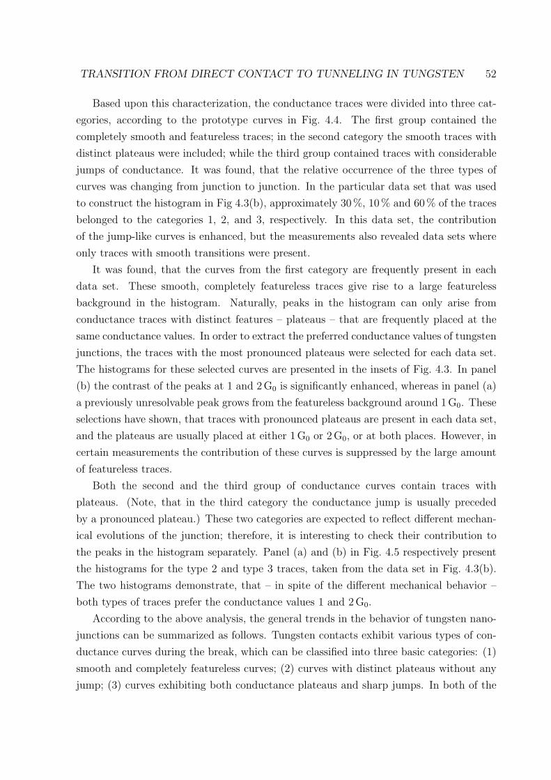
TRANSITION FROM DIRECT CONTACT TO TUNNELING IN TUNGSTEN 52
Based upon this characterization, the conductance traces were divided into three cat-
egories, according to the prototype curves in Fig. 4.4. The first group contained the
completely smooth and featureless traces; in the second category the smooth traces with
distinct plateaus were included; while the third group contained traces with considerable
jumps of conductance. It was found, that the relative occurrence of the three types of
curves was changing from junction to junction. In the particular data set that was used
to construct the histogram in Fig 4.3(b), approximately 30 %, 10 % and 60 % of the traces
belonged to the categories 1, 2, and 3, respectively. In this data set, the contribution
of the jump-like curves is enhanced, but the measurements also revealed data sets where
only traces with smooth transitions were present.
It was found, that the curves from the first category are frequently present in each
data set. These smooth, completely featureless traces give rise to a large featureless
background in the histogram. Naturally, peaks in the histogram can only arise from
conductance traces with distinct features – plateaus – that are frequently placed at the
same conductance values. In order to extract the preferred conductance values of tungsten
junctions, the traces with the most pronounced plateaus were selected for each data set.
The histograms for these selected curves are presented in the insets of Fig. 4.3. In panel
(b) the contrast of the peaks at 1 and 2 G0 is significantly enhanced, whereas in panel (a)
a previously unresolvable peak grows from the featureless background around 1 G0. These
selections have shown, that traces with pronounced plateaus are present in each data set,
and the plateaus are usually placed at either 1 G0 or 2 G0, or at both places. However, in
certain measurements the contribution of these curves is suppressed by the large amount
of featureless traces.
Both the second and the third group of conductance curves contain traces with
plateaus. (Note, that in the third category the conductance jump is usually preceded
by a pronounced plateau.) These two categories are expected to reflect different mechan-
ical evolutions of the junction; therefore, it is interesting to check their contribution to
the peaks in the histogram separately. Panel (a) and (b) in Fig. 4.5 respectively present
the histograms for the type 2 and type 3 traces, taken from the data set in Fig. 4.3(b).
The two histograms demonstrate, that – in spite of the different mechanical behavior –
both types of traces prefer the conductance values 1 and 2 G0.
According to the above analysis, the general trends in the behavior of tungsten nano-
junctions can be summarized as follows. Tungsten contacts exhibit various types of con-
ductance curves during the break, which can be classified into three basic categories: (1)
smooth and completely featureless curves; (2) curves with distinct plateaus without any
jump; (3) curves exhibiting both conductance plateaus and sharp jumps. In both of the
TRANSITION FROM DIRECT CONTACT TO TUNNELING IN TUNGSTEN 53
1 2 3
a
1 2 3
b
cou
nts
[a.u
.]conductance [2e2/h]
Figure 4.5: Histograms for selected parts of the data set of Fig. 4.3. In panel (a) just thesmooth traces with distinct plateaus are included (≈ 10% of all traces). Panel (b) shows ahistogram for the curves with distinct conductance jumps (≈ 60% of all traces). The twopanels have the same vertical scale, and both histograms are normalized to the number ofcurves included.
last two categories the conductance plateaus are preferably positioned around 1 G0 and/or
2 G0.
4.4 Discussion of the results
It has been shown that the break of tungsten nanojunctions happens in a rich variety of
ways, as reflected by the diverse types of conductance traces. This behavior strikingly
differs from the usual nature of contact fracture. Of course the detailed evolution of
conductance during the disconnection of the electrodes is always irreproducible, however
– in the metallic contacts studied so far – the general shape of the conductance traces
always follow the same (material-specific) pattern. Especially, the adhesive jumps have
been found to be an unavoidable attendant of contact formation or breakage. In contrast,
we have found that in tungsten nanojunctions these sudden jumps are occasionally absent,
and the evolution of the conductance can be continuously monitored even at ultra small
electrode separations. The reason for this unique behavior of tungsten, and the possible
origin of the two peaks in the conductance histogram are discussed in this section.
In general, the break of nanojunctions occurs via a series of elastic and plastic de-
formations. The elastic behavior of the material is basically determined by the strength
of the bonds between the atoms, thus it is expected to be similar at any length-scale
down to the atomic sizes. Indeed, precise force measurements on atomic-sized contacts
have pointed out that the elastic stages of the deformation are well-described by the bulk
elastic modulus of the material [22]. In contrast, on nanoscale the plastic behavior of
matter is significantly different from the bulk properties. The main reason for that is the
fact, that the plastic deformations are aided by the motion of dislocations, which might

TRANSITION FROM DIRECT CONTACT TO TUNNELING IN TUNGSTEN 54
Figure 4.6: Illustration of different contact types. (a) – contact with large opening angle.(b) – contact with small opening angle. (c) – junction where the electrode surfaces are notperpendicular to the contact axis.
be absent in nanometer-sized volumes. This results in a highly enhanced strength against
plastic deformations [7]. On the other hand, atomic-sized junctions have a high surface-
to-volume ratio, and consequently the surface energy effects might play a crucial role in
the plastic deformations. From this reason one may expect a liquid-like behavior in the
final stages of contact fracture [7]. Due to the complexity of the processes involved, it is
hard to predict the nature of contact fracture in a certain system. An important type of
contact fracture is the so-called rupture. In this case a neck is pulled between the two
sides. During the process of rupture the minimal cross section of the neck is continuously
reduced through a series of plastic deformations. In the other extreme case – called brittle
fracture – the break takes place prior to any plastic deformations.
The very last stage of the break – the transition from direct contact to tunneling – is
governed by the the competition between the adhesive and tensile forces. The tensile forces
are determined by the stiffness of the electrodes, which is composed from the stiffness of
the nanoscale junction itself and the stiffness of the whole setup. The latter might have
significant importance in an atomic force microscope with a soft cantilever, however it is
not expected to play any role in an MCBJ due to the rigid sample mounting. The stiffness
of the junction depends on the strength of the bonds in the material, but also the junction
geometry and the crystallographic orientation of the electrodes have a crucial influence
on it. Contacts with large opening angle (Fig. 4.6a) have large stiffness, while in contacts
with small opening angle (Fig. 4.6b) a large number of layers are involved in the elastic
deformation and thus the stiffness is reduced. The stiffness is also reduced, if the contact
surfaces are not perpendicular to the contact axis (Fig. 4.6c). Then, the electrodes can
bend like a cantilever and the elastic behavior is defined by the smaller shear forces.
The conductance traces of the metals studied so far indicate that the contacts break

TRANSITION FROM DIRECT CONTACT TO TUNNELING IN TUNGSTEN 55
through the process of rupture. In this case the contact geometry is “self-organized”
during the neck pulling, and the conditions for the adhesive jumps are approximately the
same during each fracture. In contrast, our measurements imply, that tungsten breaks
in a “more brittle” way, and a large variety of contact geometries are established during
the fractures. Additionally, the bulk elastic modulus of tungsten (EW = 411 GPa) is
outstandingly large among all metals. (As a comparison the Youngs modulus of Au, Pt,
and Nb is EAu = 78 GPa, EPt = 168 GPa, and ENb = 105 GPa, respectively.) Therefore,
in “stiff” contact geometries the elastic forces can overcome the adhesion and thereby
enable a smooth transition between tunneling and direct contact, while in softer contact
geometries the adhesive jumps are still present.
This interpretation can be tested by comparing the mechanical behavior during the
break of further metals with different elastic modulus. For this reason we performed
measurements on two neighbors of tungsten in the periodic system, molybdenum and
tantalum. The elastic modulus of molybdenum is relatively large (EMo = 329 GPa), while
tantalum is much softer (ETa = 186 GPa). In agreement with that we found that tantalum
always breaks in a jump-like way, while in molybdenum a part of the conductance traces
showed a smooth transition.
Concerning the electronic properties of tungsten junctions, a special attention should
be focused on the smooth transitions to tunneling with distinct plateaus around the first
two conductance quanta (like curve 2 in Fig. 4.4). These traces have a similar pattern
to the conductance curves of ballistic point contacts in two dimensional electron gas
systems (see Fig. 2.10b). In 2DEG systems the smooth plateaus at integer multiples
of 2e2/h are a pure consequence of conductance quantization in an adiabatic channel of
free electrons. Therefore, it is tempting to attribute the similar curves of tungsten to
conductance quantization as well. It might be argued, that conductance quantization
can be observed due to the absence of sudden atomic rearrangements. In spite of the
attractiveness of this interpretation, it must be discarded from several reasons. First of all
both theoretical calculations and experiments have shown, that the conductance channels
of polyvalent metals are not expected to have perfect transmissions. There is no particular
reason to consider tungsten as an exception. Furthermore the peaks in the conductance
histograms of tungsten are rather broad, and sometimes they are shifted to higher values
(up to 1.2 G0 and 2.2 G0). In the case of conductance quantization they should be precisely
placed at the quantized values. As a further justification, the distance between the two
plateaus in tungsten junctions is extremely small ( 30 pm). If a free electron gas is
considered, a new channel can only open upon such a small electrode displacement, if
the constriction has a wide opening angle, close to 90 degrees. In such orifice-like point-

TRANSITION FROM DIRECT CONTACT TO TUNNELING IN TUNGSTEN 56
contacts the conductance quantization must be completely suppressed (see Fig. 2.11). An
alternative interpretation for the observed plateaus can be be formulated as follows. As
known from theoretical calculations, the conductance channels of single atom contacts
are connected to electron orbitals. The spatial distribution of various orbitals is different.
Therefore – due to the complete absence of adhesive jumps – the conductance channels
might close sequentially as the electrodes are disconnected: the overlap between different
orbitals decays at different electrode separations.
For transition d-metals five conductance channels are expected to contribute to the
conductance of a single-atom contact according to the number of valence orbits. The
transmission values of these conductance channels were extensively studied for single-atom
niobium junctions by tight binding calculations [23] and by measuring subgap structure in
the superconducting state [25]. The calculations performed for a simple one-atom contact
geometry revealed a single dominant channel (as a result of the hybridization between
the s and dz2 orbits), two medium-sized channels and two smaller channels which yield
together a net conductance of G = 2− 3 G0. Both the conductance and the transmission
coefficients showed a good agreement with the values determined from the experiment.
Such a detailed investigation of the transmission eigenvalues is not available for the rest
of the d-metals, and therefore the conduction properties of monoatomic contacts can only
be deduced from the conductance histograms. For all the non-magnetic transition metals
studied so far (Nb, V, Rh, Pd, Ir, Pt) the histograms show a single well-defined peak
centered in the region of G = 1.5−2.5 G0. These peaks are attributed to the conductance
of a single-atom contact [7]. To date, theoretical calculations have not been performed
for the conductance of a single-atom tungsten contact, but its value is presumably in the
same range of G = 1.5 − 2.5 G0.
In tungsten the first peak in the histogram is situated at 1 G0, which is too low to
be attributed to a single atom contact with all the channels open. Therefore, rather the
second peak at 2 G0 is interpreted as the conductance of a monoatomic contact geometry,
where the center atom is closely bound to both electrodes. The peak at 1 G0 is presumably
related to an arrangement where the electrodes are so much separated that only a part
of the electronic states have noticeable overlap.
It is well known from STM studies that tungsten surfaces have long protruding surface
modes, which have a crucial role in achieving atomic resolution. First principle calcula-
tions for the W(001) surface demonstrated that the tunnel current is primarily generated
by the 5dz2 dangling-bond surface states [43, 44]. At distances > 2 A from the nuclei the
charge density of the surface state is much higher than that of the atomic 6s-state [45]
and so the surface states play a key role in the electron transport at small separations.
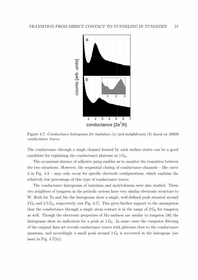
TRANSITION FROM DIRECT CONTACT TO TUNNELING IN TUNGSTEN 57
a
1 2 3 4 5 6 7
bco
unts
[arb
. uni
ts]
conductance [2e2/h]
1 2 3
Figure 4.7: Conductance histograms for tantalum (a) and molybdenum (b) based on 20000conductance traces.
The conductance through a single channel formed by such surface states can be a good
candidate for explaining the conductance plateaus at 1 G0.
The occasional absence of adhesive jump enables us to monitor the transition between
the two situations. However, the sequential closing of conductance channels – like curve
2 in Fig. 4.4 – may only occur for specific electrode configurations, which explains the
relatively low percentage of this type of conductance traces.
The conductance histograms of tantalum and molybdenum were also studied. These
two neighbors of tungsten in the periodic system have very similar electronic structure to
W. Both for Ta and Mo the histograms show a single, well-defined peak situated around
2 G0 and 2.5 G0, respectively (see Fig. 4.7). This gives further support to the assumption
that the conductance through a single atom contact is in the range of 2 G0 for tungsten
as well. Though the electronic properties of Mo surfaces are similar to tungsten [46] the
histograms show no indication for a peak at 1 G0. In some cases the computer filtering
of the original data set reveals conductance traces with plateaus close to the conductance
quantum, and accordingly a small peak around 1 G0 is recovered in the histogram (see
inset in Fig. 4.7(b)).

TRANSITION FROM DIRECT CONTACT TO TUNNELING IN TUNGSTEN 58
4.5 Conclusions
In conclusion, the results presented have shown that the evolution of conductance during
the break of tungsten nanojunctions essentially differs from the usual behavior of metallic
contacts. Due to the large elastic modulus of W and the non-ductile contact fracture,
the adhesive jumps in the conductance traces are occasionally absent. Thank to these
completely smooth transitions from direct contact to tunneling, the closing of conductance
channels can be continuously monitored at ultra small electrode separations. The study of
conductance histograms has shown, that the preferential values of conductance in tungsten
junctions are 1 G0 and 2 G0. The smooth conductance traces with plateaus at these
two values are explained by the sequential closing of conductance channels due to their
different spatial distribution. The conduction through the long-protruding surface states
of tungsten might be responsible for the plateaus at 1 G0.
Due to the limitations of the MCBJ technique a more exact and persuasive conclusion
cannot be drawn based on the results presented. The current data can greatly be improved
by simultaneous measurements of the conductance and the forces in the course of electrode
approach for contacts with a well defined tip/sample shape and orientation.

Chapter 5
Locally overheated point contacts
In this chapter experiments on locally overheated Pb and Al break junctions are presented.
At low bias voltage (Vb ≈ 10 mV), the conductance of the contact increases monotonically
as the electrodes are continuously pushed together. In contrast, at elevated bias voltage
the conductance was found to grow only to a certain value and to saturate around a
constant level during subsequent electrode approach. This part of the trace shows strong
fluctuations around the mean value, which is attributed to intense atomic rearrangements.
These phenomena are caused by the local overheating of the junction due to the high bias
voltage. The details of this basic observation, and a possible interpretation is given in the
following.
5.1 Introduction
It is well-known from elementary studies that a power of V 2/R is dissipated in a resistor
if a voltage is applied on it. This power dissipation heats up the resistor if the cooling is
not sufficient, which is a crucial difficulty in various technological applications.
In point contacts the power dissipation is concentrated in a small volume around the
contact center. This implies that the contact is heated locally by the applied voltage.
Assuming that the heat is conducted just by the electrons, the equations of the heat
conduction can be solved for a point contact geometry [47]. These calculations are valid
in the so-called thermal regime, where the contact diameter is larger than the inelastic
diffusive length (d > Li). In this case the temperature of the contact center is determined
by the bias voltage, Vb in the following way:
T 2PC = T 2
bath +V 2
b
4L , (5.1)
59
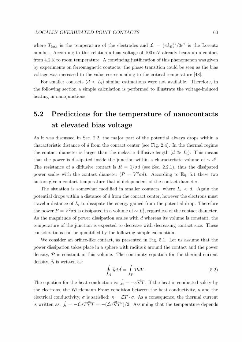
LOCALLY OVERHEATED POINT CONTACTS 60
where Tbath is the temperature of the electrodes and L = (πkB)2/3e2 is the Lorentz
number. According to this relation a bias voltage of 100 mV already heats up a contact
from 4.2 K to room temperature. A convincing justification of this phenomenon was given
by experiments on ferromagnetic contacts: the phase transition could be seen as the bias
voltage was increased to the value corresponding to the critical temperature [48].
For smaller contacts (d < Li) similar estimations were not available. Therefore, in
the following section a simple calculation is performed to illustrate the voltage-induced
heating in nanojunctions.
5.2 Predictions for the temperature of nanocontacts
at elevated bias voltage
As it was discussed in Sec. 2.2, the major part of the potential always drops within a
characteristic distance of d from the contact center (see Fig. 2.4). In the thermal regime
the contact diameter is larger than the inelastic diffusive length (d Li). This means
that the power is dissipated inside the junction within a characteristic volume of ∼ d3.
The resistance of a diffusive contact is R = 1/σd (see Sec. 2.2.1), thus the dissipated
power scales with the contact diameter (P = V 2σd). According to Eq. 5.1 these two
factors give a contact temperature that is independent of the contact diameter.
The situation is somewhat modified in smaller contacts, where Li < d. Again the
potential drops within a distance of d from the contact center, however the electrons must
travel a distance of Li to dissipate the energy gained from the potential drop. Therefore
the power P = V 2σd is dissipated in a volume of ∼ L3i , regardless of the contact diameter.
As the magnitude of power dissipation scales with d whereas its volume is constant, the
temperature of the junction is expected to decrease with decreasing contact size. These
considerations can be quantified by the following simple calculation.
We consider an orifice-like contact, as presented in Fig. 5.1. Let us assume that the
power dissipation takes place in a sphere with radius b around the contact and the power
density, P is constant in this volume. The continuity equation for the thermal current
density, jt is written as: ∮A
jtd A =
∫V
PdV . (5.2)
The equation for the heat conduction is: jt = −κ∇T . If the heat is conducted solely by
the electrons, the Wiedemann-Franz condition between the heat conductivity, κ and the
electrical conductivity, σ is satisfied: κ = LT · σ. As a consequence, the thermal current
is written as: jt = −LσT ∇T = −(Lσ∇T 2)/2. Assuming that the temperature depends

LOCALLY OVERHEATED POINT CONTACTS 61
Figure 5.1: Model for calculating the temperature in an orifice-like contact with diameter“d”. The power is dissipated in a sphere with radius “b” around the contact center.
only on the distance from the contact center, r, the continuity equation can be integrated:
2πr2Lσd
drT 2 = −4
3πb3P, if r > b (5.3)
2πr2Lσd
drT 2 = −4
3πr3P, if r < b. (5.4)
The boundary condition is: T → Tbath at r → ∞. The solution of the differential
equations is demonstrated in Fig. 5.2. In a voltage biased measurement the power density
2
2TPC
Tbath
0 b
T2(r)
r
T 2PC = T 2
bath +Pb2
Lσ− 1
3PLσ
r2, if r < b
T 2PC = T 2
bath +23Pb3
Lσ
1r, if r > b
Figure 5.2: The temperature as the function of the distance from the contact center.
is: P = (V 2b /R)/(4πb3/3). The resistance of a diffusive contact is R = 1/σd, so the
temperature of the junction at r = 0 is:
T 2PC = T 2
bath +3
4π
V 2b
Ld
b. (5.5)
In the thermal regime the power is dissipated in a characteristic distance of d from the
contact center, thus b = d should be substituted into the above equation. The result
agrees with Eq. 5.1 apart from a small deviation in the numerical prefactor.
As this simple calculation reproduces the formula the thermal limit, it could also be
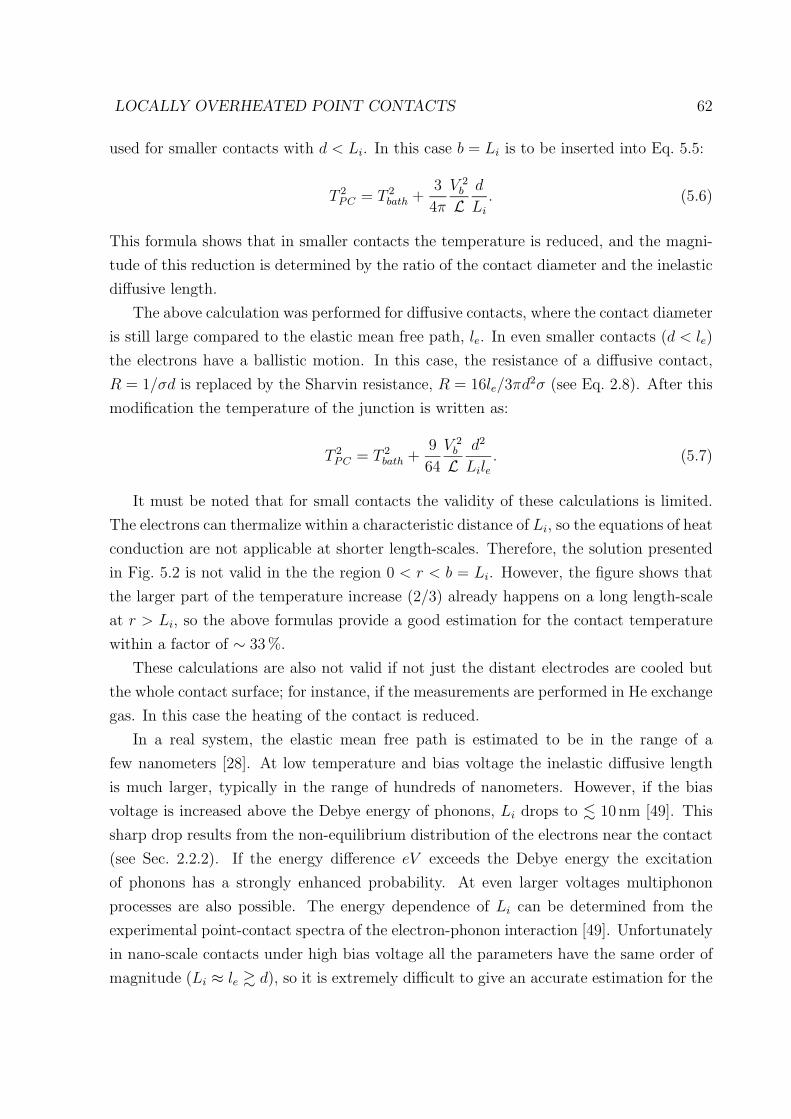
LOCALLY OVERHEATED POINT CONTACTS 62
used for smaller contacts with d < Li. In this case b = Li is to be inserted into Eq. 5.5:
T 2PC = T 2
bath +3
4π
V 2b
Ld
Li
. (5.6)
This formula shows that in smaller contacts the temperature is reduced, and the magni-
tude of this reduction is determined by the ratio of the contact diameter and the inelastic
diffusive length.
The above calculation was performed for diffusive contacts, where the contact diameter
is still large compared to the elastic mean free path, le. In even smaller contacts (d < le)
the electrons have a ballistic motion. In this case, the resistance of a diffusive contact,
R = 1/σd is replaced by the Sharvin resistance, R = 16le/3πd2σ (see Eq. 2.8). After this
modification the temperature of the junction is written as:
T 2PC = T 2
bath +9
64
V 2b
Ld2
Lile. (5.7)
It must be noted that for small contacts the validity of these calculations is limited.
The electrons can thermalize within a characteristic distance of Li, so the equations of heat
conduction are not applicable at shorter length-scales. Therefore, the solution presented
in Fig. 5.2 is not valid in the the region 0 < r < b = Li. However, the figure shows that
the larger part of the temperature increase (2/3) already happens on a long length-scale
at r > Li, so the above formulas provide a good estimation for the contact temperature
within a factor of ∼ 33 %.
These calculations are also not valid if not just the distant electrodes are cooled but
the whole contact surface; for instance, if the measurements are performed in He exchange
gas. In this case the heating of the contact is reduced.
In a real system, the elastic mean free path is estimated to be in the range of a
few nanometers [28]. At low temperature and bias voltage the inelastic diffusive length
is much larger, typically in the range of hundreds of nanometers. However, if the bias
voltage is increased above the Debye energy of phonons, Li drops to 10 nm [49]. This
sharp drop results from the non-equilibrium distribution of the electrons near the contact
(see Sec. 2.2.2). If the energy difference eV exceeds the Debye energy the excitation
of phonons has a strongly enhanced probability. At even larger voltages multiphonon
processes are also possible. The energy dependence of Li can be determined from the
experimental point-contact spectra of the electron-phonon interaction [49]. Unfortunately
in nano-scale contacts under high bias voltage all the parameters have the same order of
magnitude (Li ≈ le d), so it is extremely difficult to give an accurate estimation for the

LOCALLY OVERHEATED POINT CONTACTS 63
contact temperature. Still, the above considerations imply that a bias voltage of a few
hundred millivolts can cause considerable heating in a nanojunction. In the following the
experimental consequences of this local heating are discussed.
5.3 Experimental details
In the experiments Al and Pb contacts were investigated by measuring conductance traces
(as described in Sec. 3.4.1) during slow, continuous approach of the electrodes. The
shape of the traces was studied as a function of the bias voltage and the speed of the
electrode approach, S. These measurements required large electrode displacements, so
the modified sample mounting with two fibre glass plates was applied (see Fig. 3.4). With
this modification an electrode displacement of 20− 30 nm could be achieved in the whole
range of the piezo driver. If the fine details of the dynamical evolution of the junction
were of interest, some fragments of the conductance traces were simultaneously recorded
by the National Instruments data acquisition board with fast sampling rate (10000 pt/s).
Most of the measurements were performed at T = 4.2 K in He exchange gas under
atmospheric pressure. In such environment the electrodes are cooled much more efficiently
than in high vacuum. Therefore, the local heating is concentrated on the center of the
junction, and the thermal expansion in the farther parts of the electrodes is avoided. In He
environment the tunneling curves have a strong deviation from the exponential behavior
(see Sec. 3.4.1); so the calibration of the electrode displacement (and accordingly the
speed of the electrode approach) did not have a precision better than 25 − 30 %.
5.4 The saturation of the conductance traces at ele-
vated bias voltage
A typical conductance trace for a Pb junction recorded at an approach rate of ∼ 30 pm/s
and a bias voltage of 180 mV is presented in Fig. 5.3. After the transition from tunneling
to direct contact the conductance of the junction increases up to G ≈ 250−300 G0. After
that the conductance remains nearly constant during further electrode approach over a
distance of ≈ 22 nm. At that point the electrodes were retracted back. The break of the
contact shows a huge hysteresis with respect to its formation. This hysteresis implies,
that the electrodes were shortened by ≈ 22 nm during the measurement.
The above observation indicates a continuous transfer of atoms away from the central
region of the contact. This can be explained by the surface diffusion from the over-
LOCALLY OVERHEATED POINT CONTACTS 64
Displacement (nm)
0 5 10 15 20 251E-4
1E-3
0.01
0.1
1
10
100
1000
Co
nd
ucta
nce
(2e
/h)
2
Figure 5.3: The conductance of a Pb junction as a function of the electrode displacementat a bias voltage of 180mV and an electrode approach of 30 pm/s.
heated neck to colder areas of the electrodes. The saturation of the conductance trace
is attributed to a “feedback” process of natural origin. In the first part of the electrode
approach the conductance of the contact is continuously increasing. In a voltage biased
measurement this also means a continuous increase of power dissipation. As discussed
above, at Li d the volume where this power is dissipated remains the same (≈ L3i ), thus
the temperature of the junction increases. At a certain temperature the surface diffusion
starts to play an important role, which works against the growth of the junction. Finally
a balance develops between the enlargement of the contact due to the electrode approach
and the shrinking due to the diffusion.
In accordance with the model proposed, the value of the saturation can be tuned
by the applied bias voltage and the speed of the electrode approach. Due to the irre-
producibility of the conductance traces, no quantitative analysis of these aspects can be
done, still the general tendencies are clearly manifested. At a slow speed (≈ 10 pm/s) the
increase of the bias voltage yields lower and lower limits for the accessible conductance
values during the electrode approach. This aspect is discussed in detail in the following
paragraphs. The increase of the approach rate causes similar effects to the decrease of the
bias voltage. Above the approach rate of ≈ 1 nm/s, the traces did not show any noticeable
deviation from the standard low-bias behavior in the whole voltage range applied in the
measurements (≤ 1 V).
It must be noted, that at elevated bias voltage the junction is not just heated, but the
atoms are also “pushed” by the huge current density of the electrons. At a bias voltage of

LOCALLY OVERHEATED POINT CONTACTS 65
0 200 400 6000 2 4 6 8
5050
6060
7070
CountsDisplacement (nm)
Con
duct
ance
(2e
2 /h) a b
Figure 5.4: Panel (a) – Conductance trace of a Pb junction recorded at a bias voltage of280mV and an approach rate of 40 pm/s. (Only 5% of the measured points are plotted).Panel (b) shows the histogram for the conductance trace in panel (a).
100 mV the current density is approximately ∼ 1014 A/m2. (Note, that the conductance
of a ballistic contact is proportional to the contact area; therefore, the current density is
determined just by the bias voltage, and it does not depend on the contact size.) At such
current density, the electron-wind can exercises a force of ∼ 0.1 nN on the atoms [50].
As a comparison, a typical force of 2 nN is necessary to attain an atomic rearrangement
in a nanojunction (see Fig. 2.13) This electron-wind force is not enough large to break a
bond, but its influence must be taken into consideration, especially if the bias is further
increased.
At bias voltages of Vb ≈ 250−300 mV and an approach rate of 40 pm/s the conductance
already saturates at 40− 80 G0. An example of the flat part for such a conductance trace
is presented in Fig. 5.4a. In order to observe this saturation, approximately 10 atoms
must leave the contact area in one second. This means, that the diffusion is a rather slow
process. On the other hand the conductance rapidly fluctuates even on the timescale of the
measurements (0.1 ms). These random fluctuations are attributed to the intense atomic
rearrangements due to the voltage-induced heating of the junction. The conductance
histogram for this scan is presented in panel (b), showing a continuous, nearly gaussian
distribution.
At bias voltages of ≈ 300−400 mV the conductance cannot increase above ∼ 20 G0, as
shown in Fig. 5.5a. For this, approximately 1−3 atoms must leave the contact area in one
second. The trace shows distinct plateaus connected by sharp jumps or oscillations of the
conductance. The conductance histogram for this curve shows peaks at the positions of
the plateaus (Fig. 5.5b). A fragment of such a conductance trace is presented in Fig. 5.6.
The conductance shows a telegraph fluctuation between six distinct conductance values.

LOCALLY OVERHEATED POINT CONTACTS 66
0 1000 2000 30000 2 4 6 8 10 12 1400
22
44
66
88
1010
1212
1414
1616
1818
CountsDisplacement (nm)
Con
duct
ance
(2e
2 /h) a b
Figure 5.5: Panel (a) – Conductance trace of an Al junction recorded at Vb = 340mV andS = 40 pm/s. Panel (b) shows the histogram for this conductance trace.
0 200 400 6000 10 20 30 40 503.53.5
4.04.0
4.54.5
5.05.0
5.55.5
6.06.0
6.56.5
7.07.0
CountsDisplacement (pm)
Con
duct
ance
(2e
2 /h) a b
Figure 5.6: Panel (a) – Short fragment of a conductance trace for an Al junction (Vb =350mV and S = 30 pm/s). Panel (b) shows the histogram for this fragment.
Such a behavior was observed in several cases: due to the thermal activation the contact
can jump between various metastable configurations.
At bias voltages larger than 400 mV even the single atom contacts are not stable any
more. During continuous approach of the electrodes the junction is repeatedly jumping
between the tunneling regime and direct contacts with one or a few atoms in the cross
section. The sudden break of the contact just after its formation is probably caused by
the large current density.

LOCALLY OVERHEATED POINT CONTACTS 67
5.5 Conclusions
The measurements have shown that the heating of the contact by the elevated bias voltage
has a strong effect on the conductance traces. The enhanced temperature of the junction
and the large current density cause intense atomic rearrangements in the junction and
diffusion of atoms out of the “hot spot”. At a bias voltage of 200 mV this phenomenon
is observed only at conductance values of ∼ 100 G0, but as the voltage is increased to
∼ 400 mV even the single atom contacts become unstable. It was also shown that the
time scale of the surface diffusion is slow, so the deviation of the conductance traces from
the usual low-bias behavior is only observed at very slow electrode approach.
These phenomena limit the static measurements at large bias voltages, which is a
strong restriction if nonlinear features in the current-voltage characteristics are investi-
gated (see Chap. 6). The problem can be reduced if fast measurements are performed.
One could also benefit from the local heating of the junction. A great advantage
of break junction experiments performed at liquid helium temperature is the perfect
mechanical stability and the cleanliness of the system. At elevated temperatures the
establishment of such clean and stable environment is a difficult experimental problem.
Still, some phenomena can be observed only at higher temperature. For example one can
study electronic and atomic shell effects in nanojunctions; but for that the elevated tem-
perature is necessary, otherwise the contact cannot relax to the energetically favourable
configurations. In sodium junctions these phenomena were observed at liquid nitrogen
temperature (77 K), in other metals assumably higher temperatures would be required.
Utilizing the local heating effect one could combine the enhanced mobility of the atoms
with the advantages of performing the measurements under cryogenic circumstances.

Chapter 6
Nonlinear conductance in
atomic-sized junctions
In this chapter the nonlinear conductance of Au, Al, Pt, Ni, and W atomic-sized junctions
is investigated. The possible origins of nonlinearities in the current-voltage characteris-
tics are discussed, including quantum interference effects, the voltage dependence of the
channel transmission, and the thermal expansion of the electrodes.
6.1 Introduction
The majority of the theoretical and experimental studies of quantum contacts focus on
the zero-bias conductance of the system. However, since any realistic device is supposed
to operate at finite bias voltage, a growing interest is attributed to the voltage dependence
of the conductance in atomic-sized junctions and to the related nonlinear phenomena.
The first experiments [51] revealed a highly non-linear behavior of the current-voltage
curves already in the bias voltage range < 0.5 V. The I − V curves exhibited a strong
cubic dependence, I(V ) = G1V + G3V3, with G3 > 0. These results were in obvious
disagreement with the voltage dependence of conductance histograms, where the position
of the peaks did not change as the bias was varied [52, 53]. Recently it was shown, that
the pronounced nonlinear features in the early experiments resulted from the tunnelling
through a contaminated layer between the electrodes. After routine cleaning procedures
in ultra high vacuum system, the cubic term was strongly reduced [54].
If the contamination of the junction is eliminated, the nonlinearity of the I − V curve
is hardly visible; however, after subtracting the linear conductance, several nonlinear
features can be detected on the scale of a few percents. These nonlinearities can come
from various physical phenomena, and the separation of the different processes is not
68

NONLINEAR CONDUCTANCE IN ATOMIC-SIZED JUNCTIONS 69
always an easy task. As an example, quantum interference effects give an important
contribution to the nonlinear features [27, 28]. The excitation of the vibration modes
of the junctions can also cause nonlinearity, from which the phonon frequencies can be
determined [55]. However, the latter phenomenon can only be resolved in junctions, where
the quantum interference is suppressed.
The mechanically controllable break junction technique is a perfect tool for investigat-
ing nonlinear phenomena in atomic-sized junctions. It ensures a clean environment, and
the perfect mechanical stability provides long enough time for the measurements without
any noticeable change in the junction. Due to this stability, the I − V curves can be
recorded with a high precision, so that even tiny features on the scale of 0.01 % can be
resolved. Furthermore the variation of the I − V curve along the conductance trace can
also be investigated, which requires a junction stable on the scale of an hour.
The measurements presented in this chapter provide further insight into the possible
origins of nonlinear features. First a new method is introduced to study quantum inter-
ference effects. Then the voltage dependence of the channel transmission is investigated
in various metals. Some disturbing artifacts, like the thermal expansion of the electrodes
are also discussed.
6.2 Experimental details
The measurements were performed on well-annealed polycrystalline gold, aluminium, plat-
inum, nickel, and tungsten wires with a purity of 99.99 − 99.999 %. In order to minimize
the thermal expansion of the electrodes, most of the measurements were done in He
exchange gas under atmospheric pressure.
The I−V curve of the nanojunctions were recorded as it was introduced in Sec. 3.4.3. A
typical current-voltage characteristic for a single atom Au contact is presented in Fig. 6.1a.
The nonlinearity of the curve is very small, practically invisible on this scale. In panel
(b) the nonlinear features are magnified after subtracting the linear fit. Comparing the
scales of the two panels, the nonlinearity does not exceed a few percents. The shape of the
nonlinear part showed a large variation from junction to junction. Gold and aluminum
contacts did not exhibit a nonlinearity of significantly larger amplitude, while in transition
metals the nonlinearity was somewhat larger.
The voltage range of the measurement was restricted due to the voltage-induced heat-
ing of the junction, and the electromigration, which may occur at large current densities
(see Chap. 5). These aspects can cause irreversible atomic rearrangements in the contact.
As an example, Fig. 6.2 shows jump-like changes in the I −V curve, which are attributed

NONLINEAR CONDUCTANCE IN ATOMIC-SIZED JUNCTIONS 70
-0.4 -0.2 0.0 0.2 0.4
-40
-30
-20
-10
0
10
20
30
40
-0.4 -0.2 0.0 0.2 0.4
-0.4
-0.3
-0.2
-0.1
0.0
0.1
0.2
0.3a
Cu
rre
nt (
µA)
Bias voltage (V)
b
Nonlinear part of the current (µ A
)
Bias voltage (V)
Figure 6.1: Panel (a) shows the I − V curve of a single atom gold contact. The linearfit yields a conductance of G = 0.97G0. Panel (b) shows the nonlinear part of the I − Vcurve.
to the thermal expansion of the electrodes. Any sharp jump, hysteresis, or strong noise
in the I − V curve indicates the mechanical instability of the contact; thus, the voltage
bias should only be increased to values, where these features are not yet present. For
gold contacts the limit for reproducible measurements was typically ∼ 500 mV, occasion-
ally 800 mV. In the rest of the metals studied the instabilities already appeared at
300− 400 mV. It should be noted, that these voltage limits can be expanded above 1 V if
fast measurements are performed [54], or if the electrodes are contaminated [56].
In some measurements (discussed later in Sec. 6.3.1) the slope of the conductance
trace as a function of bias voltage was also recorded. For this aim, the modified sample
mounting presented in Fig. 3.4 was applied. The right-hand side pad was a shear piezo
element, which was used to modulate the electrode separation, z. The electrode on
the shear piezo was oscillated with a sine-wave with a typical amplitude of 0.1 A and a
frequency of 1 kHz. As the bias voltage was varied, the current was detected both by
the Keithley 2400 SourceMeter and a lock-in amplifier. The SourceMeter measured the
DC component, while the lock-in determined the response to the harmonic oscillation. In
other words, the SourceMeter provided the I(V ) curve, whereas the lock-in measured the
value of ∂I/∂z as a function of the bias voltage. The slope of the plateau, ∂G/∂z was
determined by numerical differentiation from the ∂I/∂z curves.

NONLINEAR CONDUCTANCE IN ATOMIC-SIZED JUNCTIONS 71
-0.4 -0.3 -0.2 -0.1 0.0 0.1 0.2 0.3 0.4
-60.0
-40.0
-20.0
0.0
20.0
40.0
60.0
Bias voltage (V)
~ 1 G0
~ 2 G0
Cur
rent
(µA
)
Figure 6.2: I-V curve of a gold contact in cryogenic vacuum environment. The increaseof the bias voltage causes a considerable heating of the junction. Due to the thermalexpansion of the electrodes, the monoatomic contact jumps to a configuration with twiceas large conductance. As the voltage is subsequently reduced, the junction jumps back tothe original configuration with a hysteresis.
6.3 Quantum interference effects
As it was already visible in Fig. 6.1b, the measurements can resolve fine details of the
I − V characteristic. These fine oscillations are even more pronounced after numerical
differentiation, as shown in Fig. 6.3. The differential conductance, ∂I/∂V has a random
pattern; however, for the same junction it is precisely reproducible to the very small
details. On the other hand, as the junction is changed a completely new structure appears
in the nonlinearity. As it was demonstrated by Ludoph, these oscillations are a result of
quantum interference in the junction [27, 28]. The electron wave that has travelled through
the contact is partially reflected by impurities or lattice defects in the electrodes. This
reflected wave goes back to the contact, and a part of it is reflected back again by the
contact itself. This part of the wave can interfere with the direct wave (see the illustration
in Fig. 6.3). As the voltage is varied, the wavelength of the electrons is changed, so the
conditions for interference are shifting. Various electron paths, scattered on different
defects can interfere, which explains the random, oscillatory shape of the differential
conductance curves. Naturally, if the junction has a perfect transmission, the part of the
electron wave that returns the contact cannot be scattered back, so the interference is
suppressed. This phenomenon was statistically studied in the work of Ludoph, as it was
already discussed in Sec. 2.4.1.
The interference pattern could also be changed by tuning the phase factor of the
electron paths with magnetic field. However, the area enclosed by the electron paths is
so small that a field of 60 T would be required to have a considerable influence on the

NONLINEAR CONDUCTANCE IN ATOMIC-SIZED JUNCTIONS 72
-0.4 -0.2 0.0 0.2 0.40.86
0.88
0.90
0.92
0.94
0.96
0.98
1.00
1.02d
I/dV
(2
e2 /h)
Bias voltage (V)
Figure 6.3: Differential conductance of a single atom gold contact obtained by the numer-ical differentiation of the I − V curve in Fig. 6.1. The illustration demonstrates the basicmechanism behind the quantum interference effect: the direct electron wave interferes withthe wave reflected by a defect and then reflected back by the contact.
interference, while a field of 1 T already causes changes in the atomic arrangement of the
contact due to magnetostriction effects [28].
A further possibility to change the interference pattern is the variation of the path
lengths. An experimental realization of that is discussed in the following subsection.
6.3.1 The influence of quantum interference on the slope of the
conductance plateaus
The path length of the electron trajectories can be changed by tuning the electrode sep-
aration itself. Indeed, the conductance plateaus exhibit a fine structure around the mean
value during the retraction of the electrodes. As an example, Fig. 6.4 shows a part of
the last plateau in a gold junction. The variation of the conductance along the plateau
can come from the change of the transmission Tc(z) due to the change of the overlap
between the atoms. On the other hand, quantum interference can also give contribution
to the structures observed. To have a complete oscillation in the interference for a cer-
tain electron path, the electrode separation should be changed by one wavelength of the
electrons. Unfortunately such a displacement would already cause atomic rearrangement

NONLINEAR CONDUCTANCE IN ATOMIC-SIZED JUNCTIONS 73
0.4 0.6 0.8 1.0 1.2 1.40.97
0.98
0.99
1.00
1.01
Con
duct
ance
(2e
2 /h)
Piezo voltage (V)
Figure 6.4: Fine structure of the conductance plateau in a single atom gold junction. Achange of 1V in the piezo voltage corresponds to an electrode displacement of ∼ 0.7 A.
in the junction. The dependence on the electrode separation can be better studied by
measuring the slope of the plateau, ∂G/∂z as a function of the bias voltage. The meaning
of such measurements can be understood with the help of the simple model introduced in
the following.
The wave number of the electron at elevated bias voltage can be approximated as:
k = kF + eV/vF , where kF is the Fermi wave number and vF is the Fermi velocity.
If the scattered electron travels a path with length Lj before returning the contact, the
period of the oscillation in the interference pattern is ∆V = 2πvF /eLj. The differential
conductance curve in Fig. 6.3 shows clear oscillations down to the level of ∼ 50 mV, which
corresponds to an electron path of Lj 20 nm. A simple description for the transmission
of the contact with the interference corrections is given by the following formula:
T (z, V ) = Tc(z)
[1 +
∑j
Aj cos
(kF +
eV
vF
)Lj + Φj
]. (6.1)
Tc is the transmission of the contact without interference corrections; naturally it depends
on the electrode separation, z. It can also depend on the voltage, however – as discussed
later – this voltage dependence is expected to be a slowly changing function. The lengths
of the different paths are denoted by Lj, whereas Φj represents the phase factor that might
come from the details of the scattering. The amplitude Aj is determined by the length of
the path, the scattering cross section of the defect, the geometry of the constriction and
the bare transmission of the contact. Without discussing the details of this amplitude,
it can be stated that Aj decreases with increasing path length; furthermore, the summed
contribution of different paths with similar length scales with 1/L [57]. It should be
emphasized, that the path length must be smaller than the inelastic diffusive length, Li,
otherwise the coherence is lost and the amplitude Aj is zero.

NONLINEAR CONDUCTANCE IN ATOMIC-SIZED JUNCTIONS 74
-0.3 -0.2 -0.1 0.0 0.1 0.2 0.3
-0.5
0.0
0.5
1.0
-0.3 -0.2 -0.1 0.0 0.1 0.2 0.3
-0.08
-0.06
-0.04
-0.02
0.00
0.02
-20
-10
0
10
20
0.85
0.90
0.95
1.00
1.05
c
∂ I/∂
z ( µ
A/Å
)
Bias voltage (V)
d
∂G/ ∂z (2e
2/hÅ)
Bias voltage (V)
a
I (µA
)
b
G=
∂I/ ∂V (2e
2/h)
Figure 6.5: The figure shows the I(V ) curve (a), the G(V ) = ∂I/∂V curve (b), the∂I(V )/∂z curve (c), and the ∂G(V )/∂z curve of the same single-atom gold contact.
The differential conductance of the system G(z, V ) is simply the transmission T (z, V )
multiplied by the quantum conductance unit, so the formula 6.1 can be compared with
the experimental results. Panel (b) in Fig. 6.5 shows a further example of a differential
conductance curve for a single-atom gold contact, which was obtained by the numerical
differentiation of the I − V curve in panel (a). The differential conductance shows slight
oscillations which have a relative amplitude of ∼ 15 % around G = 0.94 G0. According to
Eq. 6.1 the bare transmission of the contact can be approximated by the mean value of
the differential conductance, thus Tc 0.94.
If the dependence of the differential conductance on the electrode separation, z is
attributed solely to the bare transmission Tc(z), the slope of the conductance plateau can
be written as:∂G(z, V )
∂z=
1
Tc(z)
∂Tc(z)
∂zG(z, V ). (6.2)
This means that the voltage dependence of ∂G/∂z is simply proportional to G(V ). In
contrast, experimentally the ∂G/∂z curves show much larger nonlinearities. Panel (c) in
Fig. 6.5 demonstrates the ∂I/∂z curve, which was recorded parallel with the I(V ) curve
in panel (a). The comparison of these two curves shows that the ∂I/∂z curve has a
significantly stronger deviation from the linear behavior. In panel (d) the ∂G/∂z curve is
presented which was obtained by the numerical differentiation of ∂I/∂z. The oscillatory
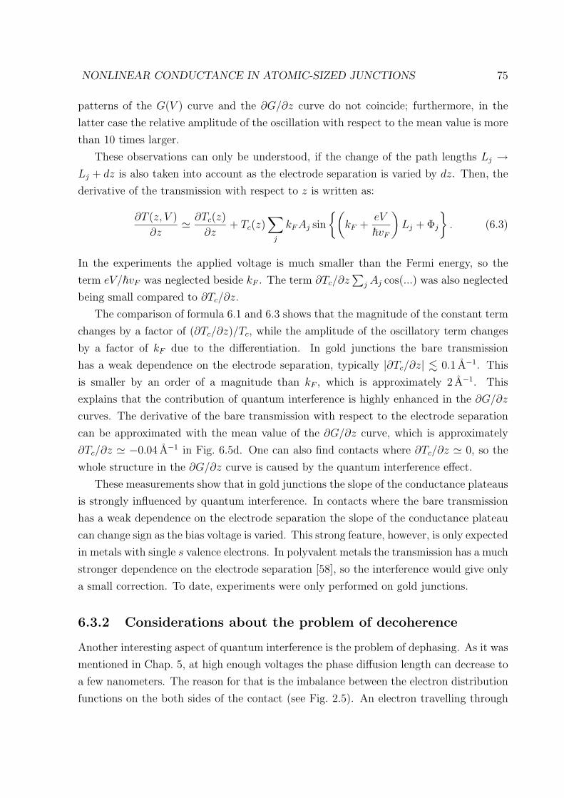
NONLINEAR CONDUCTANCE IN ATOMIC-SIZED JUNCTIONS 75
patterns of the G(V ) curve and the ∂G/∂z curve do not coincide; furthermore, in the
latter case the relative amplitude of the oscillation with respect to the mean value is more
than 10 times larger.
These observations can only be understood, if the change of the path lengths Lj →Lj + dz is also taken into account as the electrode separation is varied by dz. Then, the
derivative of the transmission with respect to z is written as:
∂T (z, V )
∂z ∂Tc(z)
∂z+ Tc(z)
∑j
kF Aj sin
(kF +
eV
vF
)Lj + Φj
. (6.3)
In the experiments the applied voltage is much smaller than the Fermi energy, so the
term eV/vF was neglected beside kF . The term ∂Tc/∂z∑
j Aj cos(...) was also neglected
being small compared to ∂Tc/∂z.
The comparison of formula 6.1 and 6.3 shows that the magnitude of the constant term
changes by a factor of (∂Tc/∂z)/Tc, while the amplitude of the oscillatory term changes
by a factor of kF due to the differentiation. In gold junctions the bare transmission
has a weak dependence on the electrode separation, typically |∂Tc/∂z| 0.1 A−1. This
is smaller by an order of a magnitude than kF , which is approximately 2 A−1. This
explains that the contribution of quantum interference is highly enhanced in the ∂G/∂z
curves. The derivative of the bare transmission with respect to the electrode separation
can be approximated with the mean value of the ∂G/∂z curve, which is approximately
∂Tc/∂z −0.04 A−1 in Fig. 6.5d. One can also find contacts where ∂Tc/∂z 0, so the
whole structure in the ∂G/∂z curve is caused by the quantum interference effect.
These measurements show that in gold junctions the slope of the conductance plateaus
is strongly influenced by quantum interference. In contacts where the bare transmission
has a weak dependence on the electrode separation the slope of the conductance plateau
can change sign as the bias voltage is varied. This strong feature, however, is only expected
in metals with single s valence electrons. In polyvalent metals the transmission has a much
stronger dependence on the electrode separation [58], so the interference would give only
a small correction. To date, experiments were only performed on gold junctions.
6.3.2 Considerations about the problem of decoherence
Another interesting aspect of quantum interference is the problem of dephasing. As it was
mentioned in Chap. 5, at high enough voltages the phase diffusion length can decrease to
a few nanometers. The reason for that is the imbalance between the electron distribution
functions on the both sides of the contact (see Fig. 2.5). An electron travelling through

NONLINEAR CONDUCTANCE IN ATOMIC-SIZED JUNCTIONS 76
Figure 6.6: Two types of electron paths. In panel (a) the interference path runs in the rightside of the contact, where the chemical potential is smaller by eV than the energy of theinterfering electron. In this case the decoherence due to phonon excitation is enhanced.In panel (b) the interference path runs in the left side of the contact. Here the chemicalpotential is the same as the energy of the electron, so the decoherence is less likely.
the junction arrives to an environment, where most of the occupied electron states have
an energy smaller by eV . If this energy exceeds the Debye energy (∼ 20 meV), there is a
large probability for exciting a phonon, and thus the coherence length strongly drops. At
even higher voltages multiphonon processes can also occur. This would imply that the
interference pattern in the I − V curves should disappear as the voltage is increased. In
contrast, the experiments shows oscillations in the whole voltage range of the measurement
(up to V = 300 − 500 mV).
A possible explanation for the absence of decoherence can be given as follows. The
enhanced probability for phonon excitation is only valid for the trajectories that cross
the contact (Fig. 6.6a). The electron waves that are reflected by the junction (Fig. 6.6b)
travel in an environment where the most of the states are occupied until the same energy,
and thus the energy relaxation is less likely. While the first type of trajectories can easily
become incoherent, the second type of paths with the same length are still contributing
to the quantum interference. Therefore, the interference pattern should not necessarily
disappear as the voltage is increased. On the other hand, the above phenomenon should
cause a certain asymmetry with respect to the sign of the bias voltage, since at different
polarity different electron trajectories give the coherent contribution to the interference.
Though, as the differential conductance curves have anyhow an irregular pattern, it would
be hard to demonstrate this polarity dependence.
NONLINEAR CONDUCTANCE IN ATOMIC-SIZED JUNCTIONS 77
-0.4 -0.2 0.0 0.2 0.4
0.87
0.90
0.93
0.96
-0.4 -0.2 0.0 0.2 0.4
1.30
1.35
1.40
1.45
1.50
-0.4 -0.2 0.0 0.2 0.4
1.4
1.5
1.6
1.7
1.8
1.9Al
dI/d
V (
2e2 /h
)
W
Bias voltage (V)Bias voltage (V) Bias voltage (V)
Pt
Figure 6.7: Differential conductance curves for an aluminum, a tungsten and a platinumcontact. Note that the vertical scales are different.
6.3.3 Differential conductance curves in other metals
Figure 6.7 shows differential conductance curves for an aluminum, a tungsten, and a
platinum junction. All the three curves show oscillations due to quantum interference.
The magnitude of the nonlinearity for aluminum is similar to gold. The amplitude of the
oscillation is similar for W and Pt as well, but the overall magnitude of the nonlinearity is
somewhat larger. It seems that in tungsten the conductance is increasing with increasing
voltage, while in platinum it is decreasing. The reason for this observation is discussed in
the next section.
6.4 Voltage dependence of the bare transmission of
the junction
The quantum interference effects resulted in random nonlinearities in the I − V curves.
The irregular pattern of the nonlinearity was precisely reproducible for a certain junction,
but as soon as the junction was changed, the shape of the nonlinearity became completely
different. The bare transmission of the contact, Tc might also be influenced by the bias
voltage. According to theoretical predictions, a considerable change in Tc is only expected
on the scale of the Fermi energy [59]. Consequently, in the voltage range of the experiments
the nonlinearity caused by this phenomenon is expected to be a smooth change without
any sharp oscillation. On the other hand, the shape of this nonlinearity is assumably
similar for different junctions of the same size. Therefore, the voltage dependence of Tc
should be reflected by a gradual but systematic nonlinearity in the I −V curve. This can

NONLINEAR CONDUCTANCE IN ATOMIC-SIZED JUNCTIONS 78
-0.2
-0.1
0.0
0.1
0.2
-0.2
-0.1
0.0
0.1
0.2NiPtW
G2 /G
1
1 2 3 4 5 6 7 8 9 10
-1
0
1
2
3
Conductance (2e2/h)
G3 /G
1
AuAl
G2/
G1
1 2 3 4 5 6 7 8 9 10
-0.6
-0.4
-0.2
0.0
0.2
0.4
0.6
G3/
G1
Conductance (2e2/h)
Figure 6.8: The normalized amplitudes of the second and the third order term from thepolynomial fit of the I − V curves, I(V ) = G1V + G2V
2 + G3V3 are shown for various
junctions. The left panel shows the results for gold and aluminum, while the right panelshows the results for nickel, platinum, and tungsten junctions.
only be detected, if its amplitude is comparable to or larger than the random oscillations
due to quantum interference.
Slowly changing deviations from the linear behavior can be well approximated by low
order polynoms. For each metal several I − V curves were recorded at different junction
sizes, and each of them was fitted with a third order function, I(V ) = G1V +G2V2+G3V
3.
The linear conductance of the system is given by G1, while the asymmetric and symmetric
part of the nonlinearity is characterized by G2 and G3, respectively. Of course, this
polynom can also approximate the low-frequency components of the quantum interference
structure; however, in this case the values of G2 and G3 for different junctions should show
a random distribution centered at zero.
In Fig. 6.8 the normalized amplitudes, G2/G1 and G3/G1 are plotted as a function
of the linear conductance, G1. For gold and aluminum junctions no special tendency is
observed, the amplitudes of both the second and the third order term scatter around
zero. This indicates, that the voltage dependence of Tc cannot be resolved within the
quantum interference. It should be noted that the typical magnitude of G2 and G3 for

NONLINEAR CONDUCTANCE IN ATOMIC-SIZED JUNCTIONS 79
gold is in good agreement with previous STM measurements on clean contacts [54]. The
figure shows, that the amplitude of the second order term is in the same range for all
the materials studied. Furthermore for each metal G2/G1 scatters around zero, thus no
systematic asymmetric deviation from the linear conductance is detected. In contrast,
the typical amplitude of the normalized cubic term, G3/G1 in transition metal junctions
is 5 − 10 times larger than in gold, and its distribution shows pronounced tendencies. In
tungsten its amplitude is always positive; and it does not decrease with increasing junction
size, as it was the case for Au and Al. In nickel the situation is more complicated: for
small junctions G3/G1 is positive, at ∼ 3 G0 it crosses zero, and at higher conductance
values it is always negative. For platinum the number of points is limited, still the figure
implies a similar behavior to nickel, just the transition from positive to negative sign
occurs at ∼ 1.5 G0.
Recently, the nonlinear conductance of Pt junctions was also studied elsewhere [60].
These experiments revealed the same systematic deviation from the ohmic behavior: above
1.5 G0 the sign of G3 was always negative, or in other words, the conductance was always
decreasing with increasing voltage. This observation was explained by first principles den-
sity functional theory calculations, which were compared for gold and platinum junctions.
The answer to the question, why Au is ohmic and Pt is not, can be briefly summarized
as follows. In gold only s electrons contribute to the conduction, for which the channel
transmission does not show noticeable dependence on the bias voltage. In platinum d elec-
trons are also involved. In this case the channels connected to dxy, dzx, and dyz orbitals
become less transparent as the voltage is increased, while the dx2−y2 channel completely
disappears. The authors predict that linear I − V curves can only be expected when
exclusively s, pz, and dz2 electrons are involved in the transmission, otherwise the com-
plex electron structure will lead to nonlinear features. The authors also show that the
stretching of the contact causes a decrease in the contribution of the d channels, which
results in the suppression of the nonlinearity.
In aluminum junctions the main contribution to the conductance comes from a channel
connected to the hybridization of s and pz orbitals, while the px and py channels have a
much smaller transmission [23]. This can explain, that no systematic voltage dependence
of the bare transmission, Tc was resolved beside the quantum interference pattern.
The results for Pt junctions can be interpreted as follows. The conductance of an un-
stretched single-atom Pt contact is G 2 G0 [61]. This means that below 2 G0 the contact
is already stretched, which results in the decrease of the nonlinearity. The observation
that below 1.5 G0 the nonlinearity increases with opposite sign might be attributed to the
enhanced contribution of tunneling electrons. In the tunneling regime the increase of the
NONLINEAR CONDUCTANCE IN ATOMIC-SIZED JUNCTIONS 80
bias voltage causes a distortion of the tunnel barrier, which increases the conductance of
the junction.
The same argumentation might be applied for nickel junctions too. However, in nickel
the cubic term changes sign at ∼ 3 G0, while the conductance of a single atom contact
is in the range of 1.3 G0. In tungsten junctions the cubic term does not change sign at
all up to 10 G0. This shows that the nonlinear features in Ni and W contacts cannot be
directly compared with the calculations for Pt junctions, and the microscopic origin of
the observations remains an open question.
6.4.1 Thermal expansion of the electrodes
Up to this point, nonlinearities due to quantum interference and the voltage dependence
of the channel transmission were discussed. In these phenomena the electronic structure
of the contact is changing as the voltage is varied. It should be noted, that nonlinearities
can also be caused by processes where the atomic arrangement of the junction is changing
with the voltage. In some sense, such processes are disturbing artifacts, which should be
eliminated or reduced to an acceptable level.
The applied voltage can induce considerable heating in the junction. Figure 6.2 demon-
strated a possible consequence of that: as the voltage is increased the thermal expansion
of the electrodes causes a sudden atomic rearrangement. Such drastic changes of the con-
tact geometry can easily be recognized from the jump-like changes in the I − V curves,
which are usually not reproducible. However, thermal expansion of smaller amplitude
might cause smooth and reproducible changes in the conductance of the junction.
The thermal expansion has a similar effect to the pushing of the electrodes by the piezo
driver. Thus, in case of thermal expansion the conductance as a function of bias voltage
should show similar pattern to the conductance traces as the piezo voltage is decreased.
Of course this effect would be accompanied with all the nonlinearities discussed before.
In order to suppress the contribution of quantum interference, the conductance G = I/V
can be measured instead of the differential conductance G = ∂I/∂V . The conductance
can be obtained after the integration of Eq. 6.1:
I
V= G0 · Tc(z)
[1 +
∑j
vF Aj
eV Lj
sin
(kF +
eV
vF
)Lj + Φj
]. (6.4)
The amplitude of the oscillatory term in this case can be compared to the one in the
differential conductance (Eq. 6.1). The ratio of the two amplitudes is vF /eV Lj. The
bottom limit for the path length, Lj is the elastic mean free path, which is approximately

NONLINEAR CONDUCTANCE IN ATOMIC-SIZED JUNCTIONS 81
5 nm [28]. This means that at V = 300 mV the interference structure in the conductance is
suppressed by a factor of > 10 with respect to the differential conductance. Furthermore,
the larger the voltage the more the interference term is suppressed.
In case of thermal expansion the electrodes are pushed together as the voltage is
increased. Therefore, the change of the conductance is symmetric with respect to the po-
larity of the voltage; whereas the amplitude of the nonlinearity scales with the magnitude
of the expansion and the slope of the conductance plateau.
Figure 6.9a shows the conductance of a single atom gold contact as the function of
electrode separation recorded at small bias voltage. The conductance changes only a few
percents; however, the conductance curve has well separated parts with markedly different
slopes. The conductance as the function of bias voltage was measured at four different
points of the conductance trace, as indicated by the arrows. The G(V ) curves (Fig. 6.9b)
show slight oscillations, but basically they have a symmetric “V” shape, which is in
agreement with the idea of thermal expansion. Curve 1 and 4 were recorded at positions
with intermediate slopes of the plateau; curve 2 was measured at the end of a completely
flat part; while curve 3 was recorded at the bottom of a steep slope. In accordance
with that the G(V ) curves at positions 1 and 4 have a nonlinearity of intermediate size,
curve 2 has a smaller nonlinearity; and curve 3 shows the largest nonlinearity. It should
be emphasized, that the whole shape of the G(V ) curve cannot be described in terms
of thermal expansion, especially at smaller voltages. Still, the correlation between the
nonlinearity and the slope of the plateau provides a convincing support for the presence
of thermal expansion. Due to the difficulty of separating nonlinearities of different origin,
it is hard to precisely determine the magnitude of the thermal expansion; but as a rough
estimate the electrodes expand by 15− 20 pm as the bias is increased to 300 mV. A more
quantitative analysis would require the statistical analysis of the above correlation for a
large amount of traces.
The above measurement was performed in a cryogenic vacuum environment. If He
exchange gas is admitted into the vacuum chamber, the cooling of the electrodes is sig-
nificantly better, and just the narrow neighborhood of the junction can be heated by the
applied voltage. This strongly decreases the magnitude of the thermal expansion [40].
The physical adsorption of He at the surface of the junction results in the modification
of local work function of the electrodes. This causes considerable changes in the tun-
neling curves, but it does not have a noticeable influence the conductance of a metallic
nanoconstrictions [35, 34]. All the measurements presented in the previous subsections
were performed with He exchange gas to minimize the thermal expansion.
At large voltages the contact is not just heated, but also a strong electron-wind force is

NONLINEAR CONDUCTANCE IN ATOMIC-SIZED JUNCTIONS 82
-0.3 -0.2 -0.1 0.0 0.1 0.2 0.3
4
3
2
1
a
Bias voltage (V)2 4 6 8
0.99
1.00
1.01
1.02
1.03
1.04
1.05
1.06
Con
duct
ance
(2e
2 /h)
4
32
1
b
Piezo voltage (V)
Figure 6.9: Panel (a) shows a part of a conductance plateau for a single atom gold contact.A change of 1V in the piezo voltage corresponds to an electrode displacement if ∼ 0.1 A.At the positions indicated by arrows G(V) curves were recorded, which are shown in panel(b).
excercised on the central atom due to the high current density. At a voltage of 100 mV the
current density through a single atom contact is ∼ 1014 A/m2. Such a current can push the
central atom with a force of ∼ 0.1 nN [50], which is already ∼ 10 % of the force necessary
to break the bond [22]. Therefore the large current can cause a slight displacement of the
central atom, which can have similar effect to the thermal expansion. However in this
case the atom moves away from one of the electrodes and comes closer to the other one,
which cannot be simulated by changing the piezo voltage. Thus, its investigation is a
more complicated task, and no attempts have been done in this direction yet. Assumably
this phenomenon also has a noticeable effect on the I − V curves; furthermore, it cannot
be eliminated by increased cooling power or fast measurements.
6.5 Conclusions
The conductance of atomic-sized junctions does not show strong deviation from the linear
behavior if the junction is not contaminated. On the other hand, on the scale of a few
percents various nonlinear features can be detected, which can originate from different
physical phenomena.
If the measurements are performed in a high vacuum environment the cooling of the
electrodes is not sufficient, and thus the change of the bias voltage can cause considerable

NONLINEAR CONDUCTANCE IN ATOMIC-SIZED JUNCTIONS 83
thermal expansion. As a consequence, the electrodes are pushed together as the voltage
is increased, which causes a symmetric nonlinearity in the G(V) curves. The amplitude of
this nonlinearity correlates with the slope of the conductance plateau. In He exchange gas
the thermal expansion is highly reduced; and thus, it does not disturb the investigation
of intrinsic nonlinear features.
An important nonlinear phenomenon arises from the quantum interference of differ-
ent electron paths. This effect causes a random oscillatory pattern in the differential
conductance curves. It was shown that quantum interference also gives an important
contribution to the fine structure of the conductance traces as the function of electrode
separation. A new method – the measurement of ∂G/∂z curves – was introduced to in-
vestigate this feature. It was shown that in gold junctions the quantum interference has
a much stronger influence on the ∂G/∂z curves than on the G(V ) curve itself.
The voltage dependence of the bare transmission of the contact was also investigated
in several metals. It was shown that in Au and Al junctions this effect is unresolvable
beside the quantum interference structure. In contrast, transition metal junctions have
a significant cubic term in the I − V curves, which might come from the suppression of
certain d channels at higher voltages.

Chapter 7
Hydrogen-assisted distortion of gold
nanowires
In this chapter the influence of adsorbed hydrogen on the behavior of gold nanojunctions
is investigated. It is found, that the hydrogen environment has a strong effect on the
conductance of atomic-sized gold junctions, which is markedly reflected by the growth
of an additional peak in the conductance histogram at 0.5 G0. The statistical analysis
of the conductance traces implies that the new peak arises due to the hydrogen-assisted
distortion of atomic gold chains.
7.1 Introduction
The conductance histograms of different metals have been studied under various experi-
mental conditions. It was found, that the peaks in the histogram arise due to the repeated
establishment of some stable atomic configurations during the breaking process. Usually
the general shape of the histogram is characteristic of the material, and it is not very
sensitive to the experimental parameters, like the temperature or the magnitude of the
bias voltage.
On the other hand, the interaction of adsorbates with the junction can influence the
evolution of the nanocontact during the rupture and can cause drastic changes in the
shape of the histogram. It was shown that the adsorption of some organic molecules on
copper nanojunctions results in the appearance of new peaks around 0.5 and 1.5 G0 [62].
Similar phenomenon was observed using gold nanowires immersed in an electrochemical
cell [63]. By changing the potential on the nanoconstriction from positive to negative
with respect to the reference electrode, the authors observed the appearance and growth
of two new peaks, again at 0.5 and 1.5 G0.
84

HYDROGEN-ASSISTED DISTORTION OF GOLD NANOWIRES 85
These studies have shown that the conductance histograms can serve as sensitive
detectors of adsorbates. The new peaks in the histogram are assumably caused by the
appearance of new, stable atomic arrangements in the modified environment. On the
other hand, the conductance histograms alone cannot tell the microscopic background of
the phenomenon. The above systems are rather complicated for theoretical calculations,
so the origin of the observations has remained an open question.
In this chapter we show that similar phenomenon can arise due to the adsorption
of hydrogen molecules on gold nanowires. Hopefully, the simplicity of this system will
open the opportunity for theoretical studies. We also show, that the detailed statistical
investigation of the conductance traces supplies useful information about the nature of
the new atomic configurations.
Quite recently, the influence of hydrogen molecules on platinum junctions was also
studied [64]. In this system the characteristic peak of platinum at 1.5 G0 disappears, and
a new peak grows in the histogram at 1 G0. The detailed studies have shown, that the
new peak is connected to the conduction through a H2 bridge between the Pt electrodes.
The comparison of these results with our observations have stimulated additional mea-
surements on Au and Pt contacts in hydrogen surrounding. These studies are presently
in progress; therefore, the detailed comparison of the two systems is not included in this
thesis.
7.2 Experimental details
In the experiments we used well-annealed, polycrystalline sample-wires with a purity of
99.99 − 99.999 %. During the measurements the temperature of the setup was varied in
the range of 4.2 − 50 K by changing the distance between the sample and the helium
surface and by connecting a temperature controller on the heating wire of the sample
holder. The ultra high purity hydrogen (99.9999 %) was first introduced into a space of
1 cm3 between two vacuum valves. Then the pressure in this volume was accurately set
by pumping, and finally the content of this volume was admitted to the vacuum pot of
the sample holder. In some measurements also a small amount of He exchange gas was
introduced into the sample space. It was found, that the presence of He does not affect
any of the results, but it improves the temperature stability of the system.

HYDROGEN-ASSISTED DISTORTION OF GOLD NANOWIRES 86
1 2 3 4 5conductance [2e2/h]
aco
unts
[a.u
.]
1 2 3 4 5
b
Figure 7.1: Conductance histograms of gold measured in an ultra-high vacuum environ-ment (a) and in the presence of adsorbed hydrogen (b). Both histograms were recorded ata bias voltage of 129mV and a temperature of 20K. The histograms were built from 10000conductance traces.
7.3 Basic observation: the appearance of a new peak
in the conductance histogram
A typical conductance histogram of gold measured in ultra high vacuum at T = 20 K
is presented in Fig. 7.1a. It agrees with earlier reported data obtained under similar
conditions [24]. The most pronounced feature of this histogram is a sharp peak at 1 G0.
The introduction of hydrogen into the vacuum pot resulted in the appearance of an
additional peak positioned close to 0.5 G0, as shown in Fig. 7.1b. In some cases a small
peak at ∼ 1.5 G0 was also visible, but due to its eventual occurrence we focus our attention
on the peak at ∼ 0.5 G0.
This basic observation was studied in detail by changing three experimental param-
eters: the temperature, the bias voltage and the amount of H2 near the contact. Even
though the quantity of gas admitted into the vacuum pot was accurately determined, no
reliable estimation for the H2 coverage of the junction can be given due to the presence

HYDROGEN-ASSISTED DISTORTION OF GOLD NANOWIRES 87
1 2 3 4 5conductance [2e2/h]
coun
ts [a
.u.]
b
1 2 3 4 5
a
Figure 7.2: Bias dependence of the conductance histograms of gold measured at T =20K in hydrogen environment. The bias voltages are 65mV (a) and 240mV (b). Thehistograms were built from 10000 conductance traces.
of different materials and unavoidable temperature gradients in the sample holder. For-
tunately, the results of the measurements were not sensitive to the precise amount. In
contrast, the other two parameters played a rather crucial role and the new peak in the
histogram was only observed in a restricted range of the temperature and the bias voltage.
The study of the temperature dependence showed that the fractional peak is only
present in the range of approximately 10− 30 K. The bias dependence of the conductance
histograms measured at a fixed temperature (20 K) is shown in Fig. 7.2. At bias voltages
100 mV the peaks of the histogram are superimposed on a large featureless background
(Fig. 7.2a). At higher bias, both the background and the relative amplitude of the peak at
0.5 G0 compared to the one at 1 G0 decrease (Fig. 7.1b); and finally above ∼ 200 mV the
peak at 0.5 G0 completely disappears (Fig. 7.2b). The absence of the new peak at elevated
temperature or bias voltage is assumably caused by the desorption of hydrogen from the
surface of the junction. These two effects can have the same origin: at elevated bias the
voltage-induced heating of the junction causes the desorption. At low temperatures the
vapor pressure of hydrogen is very small, so the amount of hydrogen near the contact is

HYDROGEN-ASSISTED DISTORTION OF GOLD NANOWIRES 88
strongly reduced.
The same measurements were performed on silver and copper contacts. In high vacuum
the histograms of these noble metals are resembling the one of gold [24]. The inclusion
of hydrogen resulted in a similar behavior with respect to the appearance of a featureless
background at low bias voltage. On the other hand, in Ag and Cu no indication for the
appearance of a new peak was observed.
Summarizing the experimental results, the addition of H2 to the contact area has two
basic observable consequences: (1) the growth of a large background signal at low bias
voltage which is present for all the materials investigated; (2) the appearance of a new
peak at 0.5 G0 in the conductance histogram of gold.
The first phenomenon is assumably caused by a large amount of H2 between the
electrodes. Due to the adsorption of hydrogen, the surface energy of the junction is
reduced. From this reason, a larger amount of atomic configurations might occur during
the break. It is also possible that an increased tunnel current can flow through the
hydrogen layers.
The second phenomenon – which is in the focus of the present study – indicates
the repeated establishment of a special atomic configuration during the last stages of
the break. This atomic configurations arises or becomes stable due to the surrounding
hydrogen molecules. The analysis of the conductance traces can provide information
about the nature of this new atomic configuration, as discussed in the following.
7.4 The nature of the conductance traces
In pure gold contacts the conductance plateau at 1 G0 is a robust feature. The conductance
traces contain this plateau almost without exception. Furthermore, this is the last plateau,
after which the contact breaks. This plateau is very flat, very long, and usually it is
precisely positioned at 1 G0. These features are reflected by the exceptionally sharp
peak in the conductance histogram (Fig. 7.1a). There is some chance for having smaller
conductance values down to 0.6 G0, but below that there are absolutely no counts in the
histogram.
The appearance of a new peak around 0.5 G0 raises the question, how these strong
features of the conductance traces of pure gold are modified in the presence of hydrogen.
Naturally, the traces must contain plateaus both at 0.5 G0 and at 1 G0. However, the
conductance histogram alone cannot tell how these plateaus are related to each other.
Figure 7.3a shows a conductance trace extracted from the data set. It has plateaus at both
conductance values: first the conductance stays at 1 G0, then it jumps to 0.5 G0, and finally

HYDROGEN-ASSISTED DISTORTION OF GOLD NANOWIRES 89
0 50 100 150 200 250 300 3500
1
2
3
4
5
6
7
8
T ime [ms ]
Co
nd
uct
an
ce[2
e2/h
]
0 10 20 30 400
1
2
3
4
Con
duct
ance
[2e2 /h
]
Time [ms]
Figure 7.3: Conductance traces of hydrogen-covered gold junctions. Panel (a) shows atrace with a long plateau at 1G0 followed by a shorter plateau at 0.5G0. The traces inpanel (b) show telegraph fluctuation between 1G0 and 0.5G0.
the contact breaks. This kind of behavior was frequent, but not exclusive. Another two
examples are presented in Fig. 7.3b. These traces show a telegraph fluctuation between
0.5 G0 and 1 G0. This telegraph fluctuation implies that the contact can choose from
two metastable atomic configurations. The one with unit conductance is assumably the
customary atomic arrangement of pure gold. The other one with G = 0.5 G0 is another
– yet unknown – configuration which is only observable if hydrogen molecules are also
present. It should be noted that plateaus at 0.5 G0 are not seen in each trace, several
conductance curves look like those in pure gold contacts. On the other hand, traces with
plateau at 0.5 G0 and no plateau at 1 G0 were not typical.
The plateaus are not precisely placed at 1 G0 and 0.5 G0, which is indeed expected
from the finite width of the peaks in the histogram. The peak at 0.5 G0 grows above the
interval ∼ 0.3 − 0.75 G0, while the peak at 1 G0 grows above ∼ 0.75 − 1.1 G0. So all the
plateaus in the first interval are regarded as plateaus near 0.5 G0, while the plateaus in
the second interval are taken as plateaus near 1 G0.
Further on the lengths of these two types of plateaus are analyzed with statistical
methods.
7.5 Exploring correlations between the peaks in the
histogram
As a first step, we investigate those traces for that the plateau at 0.5 G0 is long. The
length of this plateau was determined for each trace by counting the number of data

HYDROGEN-ASSISTED DISTORTION OF GOLD NANOWIRES 90
1 2 3 4
coun
ts [
a.u.
]
conductance [2e2/h]
Figure 7.4: The area graph shows the histogram for selected 30% of the traces that havethe longest plateau at ∼ 0.5G0. The dashed line shows the histogram for the original,unselected data set. Both histograms are normalized to the number of traces included.
points in the conductance interval G/G0 ∈ [0.3, 0.75]. The data set of Fig. 7.1b contained
10000 conductance traces. From that those 3000 traces were selected, which have the
longest plateau at 0.5 G0. The histogram for these selected curves is shown in Fig. 7.4 by
the area graph. This histogram is compared with the histogram for the whole data set,
as shown by the dashed line. In order to have a good comparison, both histograms were
normalized to the number of traces included.
For the selected curves the peak at 0.5 G0 is significantly larger, which is a natural
consequence of the selection. The interesting result of this comparison is the shrinking of
the peak at 1 G0 by more than 30 % due to the selection. The rest of the structures at
higher conductance values are exactly the same on the two histograms.
This analysis shows that the traces with long plateaus at 0.5 G0 have a smaller peak at
1 G0 in the histogram; or in other words, if the plateau at 0.5 G0 is longer than in average
then the plateau at 1 G0 is shorter than in average. This kind of anticorrelation implies
that the summed length of the both plateaus is important, and the switching between
them is probably a random process. This remark will have special importance in the next
part, where the histograms for the plateau lengths are investigated.

HYDROGEN-ASSISTED DISTORTION OF GOLD NANOWIRES 91
7.6 Plateau length histograms
The measurements in a pure environment have shown, that a single atom gold contact
has a single conductance channel with perfect transmission (see Sec. 2.4.1). Furthermore
it was found that gold can form atomic chains with single atoms in a row, and this chain
also has a perfect transmission (see Sec. 2.4.2). The existence of these atomic chains was
deduced from histograms plotted for the lengths of the last plateaus before break. These
histograms revealed equidistant peaks, corresponding to the break of chains with different
number of atoms. Therefore the question must be addressed, to what extent this chain
formation is influenced by the presence of hydrogen.
As it was mentioned, even in hydrogen surrounding, a lot of traces just exhibit plateaus
at 1 G0 without any additional plateau around 0.5 G0. These traces can be regarded as
“pure gold behavior”, and the plateau length histogram for these traces can serve as a
reference (Fig. 7.5a). This histogram shows two well-defined peaks. This means that the
process of chain formation is present, but no really long chains are pulled. It should be
noted, that in metals that cannot form chains the plateau length histogram shows only a
single peak. The distance between the two peaks in Fig. 7.5a defines the Au-Au distance
in the chain.
We can also plot the plateau length histogram for the traces that have a plateau
around 0.5 G0 as well. The anticorrelation demonstrated in the previous part implies that
the summed length of the plateaus at 1 G0 and at 0.5 G0 is important. Therefore, as a
first step the plateau length is measured for each trace by the number of data points in
the conductance interval G/G0 ∈ [0.3, 1.1]. The plateau length histogram built in this
way is presented by the area graph in Fig. 7.5b. The position of the peaks coincides
with the reference histogram. The plateau length histogram for the same traces can be
plotted by measuring just the lengths of the plateaus at 1 G0. (In this case the plateau
length is the number of data points in the conductance interval G/G0 ∈ [0.75, 1.1]) This
analysis results in the histogram shown by the dashed line. In this histogram the peaks
are smeared and considerably shifted compared to the reference histogram.
A plateau at 0.5 G0 in a conductance trace is a clear sign, that the break of the
nanojunction is influenced the hydrogen molecules. The two peaks in the plateau length
histogram in Fig. 7.5b indicate that even in this case the chain formation of gold is
preserved. Furthermore, a nice plateau length histogram is only obtained if the plateaus at
0.5 G0 are also included in the plateau length. This indicates that the atomic configuration
with G = 0.5 G0 is a part of the chain formation.

HYDROGEN-ASSISTED DISTORTION OF GOLD NANOWIRES 92
0
100
200
0 40 80 120 1600
40
80C
ount
s
Length of last plateau [a.u.]
Figure 7.5: Plateau length histograms for gold junctions in hydrogen environment. Panel(a) shows the plateau length histogram for the traces that do not have any plateau in theinterval G/G0 ∈ [0.3, 0.75]. The plateau length is determined by the number of data pointsin the interval G/G0 ∈ [0.75, 1.1]. Panel (b) contains plateau length histograms for thosetraces that do have a plateau in the region G/G0 ∈ [0.3, 0.75]. The dashed line shows thehistogram for the lengths of the plateaus near 1G0. This is measured by the number ofpoints in the interval G/G0 ∈ [0.75, 1.1]. The area graph shows the histogram for the jointlengths of the plateaus around 1 and around 0.5G0. This length is given by the number ofpoints in the interval G/G0 ∈ [0.3, 1.1]
7.7 Discussion of the observations
Our measurements have shown, that the adsorption of hydrogen on gold junctions results
in the appearance of a new peak at 0.5 G0 in the conductance histogram. The same
phenomenon was not observed in silver and copper junctions, which have conduction
properties similar to gold. An important difference between the nobel metals is the
striking property that gold can form atomic chains while Ag and Cu cannot [31]. It has
already implied that the new peak at 0.5 G0 is somehow connected to the chain formation
of gold. This assumption was further supported by the investigation of plateau length
histograms. This analysis has shown that the configuration with G = 0.5 G0 is indeed a
part of the chain formation.
Local density functional simulations have shown that a small increase in the inter-
atomic distance in a Au chain causes a considerable reduction of the conductance [65].
HYDROGEN-ASSISTED DISTORTION OF GOLD NANOWIRES 93
This implies, that the configuration with perfect transmission is the usual gold chain,
while the conductance value of G = 0.5 G0 corresponds to a distorted chain with slightly
increased Au-Au distance.
This distortion can be an intrinsic property of gold, which is just aided by the hydrogen
environment. It was shown that stretched atomic chains have a tendency for spontaneous
dimerization [66, 67, 65, 68, 69]. Calculations of the conductance through a short chain
of gold atoms with a dimer yield values from 0.58 G0 [65] to 0.4 G0 [67]. Such dimers
have never been observed in high vacuum, but the adhesive hydrogen environment might
stabilize this configuration. A crucial problem with this interpretation is the following.
In a process called “dimerization” at least three atoms should be included in the chain.
In our measurements the occurrence of such long chains was not frequent (see the plateau
length histograms in Fig. 7.5), so a plausible explanation should also account for the
distortion of a chain with two atoms.
As another possibility, the binding of the hydrogen molecule on the chain itself might
cause the distortion. The precise nature of such process cannot be predicted without
microscopic model calculations. The possibility of the chemical reaction of H2 with the
gold chain also cannot be excluded.
The measurements on hydrogen covered platinum junctions have demonstrated that
the new peak in the histogram is connected to the conductance through a hydrogen
molecule [64]. In gold the plateau length histograms strongly indicate that the conduc-
tance values near 0.5 G0 are related to chains of gold atoms; therefore, the same expla-
nation is not supported. A similar analysis of the plateau length histograms can also be
performed on platinum, which has the tendency of chain formation as well. Preliminary
measurements have shown that in Pt the chain formation is completely destroyed in the
presence of hydrogen.
In conclusion, we have shown that a new stable atomic configuration appears in gold
nanojunctions due to the adsorption of hydrogen. The analysis of the results implies that
this configuration is related to a distorted chain of gold atoms. Presently, the experimental
observations cannot provide more information about the nature of this configuration.
Hopefully, the simplicity of the gold-hydrogen adsorbate system will stimulate extensive
theoretical investigations, which will lead to a better understanding of the details of
molecular adsorption on nanowires.

Conclusions
In this part the major conclusions of my Ph.D. work are summarized in five items.
1. I have built a point contact measurement system in the low-temperature solid state
physics laboratory of the Budapest University of Technology and Economics. This
work included the planning of a point-contact sample holder and the arrangement
of the instrumental environment required for the various types of point contact ex-
periments. A mechanical stability of 0.02 A/hour was achieved as demonstrated
by quantum tunneling measurements. The setup is applied in a wide range of
experiments, including the measurement of conductance traces and conductance
histograms, and the investigation of nonlinear features in the I − V characteris-
tics. Furthermore, utilizing the high stability of the device I have developed a new
method to detect quantum interference effects in nanocontacts, which is based on
the modulation of the length of the interference paths.
2. I have shown that the evolution of conductance during the break of tungsten nano-
junctions essentially differs from the usual behavior of metallic contacts. In the
metals studied so far the conductance traces always showed a similar pattern in-
cluding a jump-like transition from direct contact to tunneling. In contrast, I found
that tungsten junctions exhibit various types of conductance traces, which frequently
show a smooth transition to tunneling. This unique property of tungsten can be
attributed to the extremely large elastic modulus of the material. Due to the oc-
casional absence of the adhesive jump I could continuously monitor the decay of
the conductance channels during the disconnection of the electrodes. I have found
that the conductance traces frequently show plateaus around 1 and 2 G0, which
is explained by the sequential closing of conductance channels due to their differ-
ent spatial distribution. The plateau at 2 G0 is attributed to the conductance of a
monoatomic contact, while the plateau at 1 G0 might be interpreted by the conduc-
tance through a long-protruding surface state.
3. I have studied the influence of local Joule heating on the behavior of nanojunc-
94

CONCLUSIONS 95
tions. I have shown that at elevated bias voltage the conductance traces exhibit
a strong deviation from the standard low-bias behavior. During the approach of
the electrodes the conductance curves saturate showing strong fluctuations around
a constant level. These observations are attributed to a feedback effect due to the
enhanced surface diffusion and electromigration of atoms in the hot junction. I have
found that in atomic-sized junctions the thermal excitation of the contact leads to
repeated jumps between metastable atomic configurations.
4. I have studied the origin of non-linear features in the conductance of atomic-sized
junctions. The measurement of ∂G/∂z curves as a function of bias voltage has shown
that quantum interference has a strong influence on the slope of the conductance
plateaus in gold junctions. I have also investigated the voltage dependence of the
bare transmission in Au, Al, Pt, W, and Ni junctions. This study has shown that
in the transition metal contacts the voltage dependence of the bare transmission
gives a significant contribution to the nonlinearity of the I − V curve, while in gold
and aluminum junctions this feature is not resolved beside the quantum interference
phenomenon.
5. I have studied the influence of adsorbed hydrogen on the conductance of gold
nanowires. The hydrogen environment has a strong effect on atomic-sized gold
junctions, which is markedly reflected by the growth of a new peak in the conduc-
tance histogram at the half of the quantum conductance unit, G0 = 2e2/h. This
new peak is attributed to the repeated establishment of a special atomic configura-
tion during the break, which arises from the interaction of the gold nanoconstriction
with hydrogen. Analyzing the plateau length histograms I have shown that the new
peak in the histogram is related to an atomic gold chain which is distorted due to
the adsorption of hydrogen.

List of publications
Publications connected to my Ph.D. work:
A. Halbritter, Sz. Csonka, G. Mihaly, E. Jurdik, O. Yu. Kolesnychenko, O. I. Shklyarevskii,
S. Speller, and H. van Kempen. Transition from tunneling to direct contact in tungsten
nanojunctions. Phys. Rev. B, submitted (2003).
Sz. Csonka, A. Halbritter, G. Mihaly, E. Jurdik, O. I. Shklyarevskii, S. Speller, and H. van
Kempen Fractional conductance in hydrogen-embedded gold nanowires. Phys. Rev. Lett.,
90, 116803 (2003).
A. Halbritter, Sz. Csonka, O. Yu. Kolesnychenko, G. Mihaly, O. I. Shklyarevskii, and
H. van Kempen. Connective neck evolution and conductance steps in “hot” point-contacts.
Phys. Rev. B, 65, 45413 (2002).
L. Borda, A. Halbritter, and A. Zawadowski. Slow two-level systems in metallic point
contacts. Advances in Physics, submitted (2003), cond-mat/0107590
O. P. Balkashin, I. K. Yanson, A. Halbritter, and G. Mihaly. Point-contact spectroscopy
of the relaxation dynamics of two-level systems upon structural changes in NiNb metallic
glasses. Low Temperature Physics, 29, 123 (2003).
O. P. Balkashin, I. K. Yanson, A. Halbritter, and G. Mihaly. Microwave second-harmonic
generation and point-contact spectroscopy of Ni-Nb metallic glasses. Low Temperature
Physics, 27, 1021 (2001).
O. P. Balkashin, I. K. Yanson, A. Halbritter, and G. Mihaly. High frequency behavior
of metallic glass NixNb1−x point contacts. Solid State Commun., 118, 623 (2001).
96

LIST OF PUBLICATIONS 97
G. Mihaly, A. Halbritter, L. Mihaly, and L. Forro. Search for magnetic field induced
gap in a high-Tc superconductor. Solid State Commun., 116, 197 (2000).
A. Halbritter, A. Yu. Kolesnychenko, G. Mihaly, O. I. Shklyarevskii, and H. van Kempen.
Transport properties and point contact spectra of NixNb1−x metallic glasses. Phys. Rev. B
61, 5846 (2000).
Further publications:
J. Balogh, L. F. Kiss, A. Halbritter, I. Kezsmarki, and G. Mihaly. Giant magnetoresis-
tance at the interface of iron thin films. Solid State Commun., 122, 59 (2002).
J. Balogh, I. Vincze, D. Kaptas, T. Kemeny, T. Pusztai, L. F. Kiss, E. Szilagyi, Z. Zolnai,
I. Kezsmarki, A. Halbritter, and G. Mihaly. Interface magnetoresistance of Fe/Ag multi-
layers. Physica Status Solidi A, 183, 621 (2002).
G. Mihaly, A. Halbritter, L. Mihaly, and L. Forro. Crossovers in the out-of-plane re-
sistivity of superconducting Tl2Ba2CaCu2O8 single crystals. Europhysics Letters, 52, 584
(2000).

Acknowledgements
I would like to express my thanks to my supervisor, prof. Gyorgy Mihaly, to profes-
sors Oleg Shklyarevskii, Alfred Zawadowski, and Herman van Kempen, to my colleagues
Szabolcs Csonka, and Istvan Kezsmarki, to the technicians Laszlo Molnar, and Laszlo
Takacs, and to my parents for the help they have provided during my Ph.D. studies.
98

References
[1] K. von Klitzing. The quantized Hall effect . Rev. Mod. Phys., 58, 519 (1986).
[2] Y. Alhassid. The statistical theory of quantum dots . Rev. Mod. Phys., 72, 895 (2000).
[3] B. J. van Wees, H. van Houten, C. W. J. Beenakker, J. G. Williamson, L. P. Kouwen-
hoven, D. van der Marel, and C. T. Foxon. Quantised conductance of point contacts
in a two-dimensional electron gas. Phys. Rev. Lett., 60, 848 (1988).
[4] D. A. Wharam, T. J. Thornton, R. Newbury, M. Repper, H. Ahmed, J. E. F. Frost,
D. G. Hasko, D. C. Peacock, D. A. Ritchie, and G. A. C. Jones. One-dimensional
transport and the quantisation of the ballistic resistance. J. Phys. C, 21, 209 (1988).
[5] R. Wiesendanger. Scanning Probe Microscopy and Spectroscopy . Cambridge Univer-
sity Press, Cambridge (1994).
[6] M. F. Crommie, C. P. Lutz, and D. M. Eigler. Confinement of electrons to quantum
corrals on a metallic surface. Science, 262, 218 (1993).
[7] N. Agrait, A. L. Yeyati, and J. M. van Ruitenbeek. Quantum properties of atomic-
sized conductors . Review article, submitted to Physics Reports (cond-mat/0208239).
[8] I. K. Yanson. Nonlinear effects in the electric conductivity of point junctions and
electron-phonon interaction in metals . Sov. Phys.-JETP, 39, 506 (1974).
[9] J. C. Maxwell. A Treatise on Electricity and Magnetism. Clarendon Press, Oxford
(1904).
[10] L. Borda, A. Halbritter, and A. Zawadowski. Slow two-level systems in metallic point
contacts . Review article, submitted to Advances in Physics (cond-mat/0107590).
[11] A. G. M. Jansen, A. P. van Gelder, and P. Wyder. Point contact spectroscopy in
metals . J. Phys. C, 13, 6073 (1980).
99

REFERENCES 100
[12] Y. V. Sharvin. A possible method for studying Fermi surfaces. Sov. Phys.-JETP, 21,
655 (1965).
[13] K. S. Ralls and R. A. Buhrman. Defect interactions and noise in metallic nanocon-
strictions . Phys. Rev. Lett., 60, 2434 (1988).
[14] A. Wexler. The size effect and the non-local Boltzmann transport equation in orifice
and disk geometry . Proc. Phys. Soc., 89, 927 (1966).
[15] R. Landauer. Spatial variation of currents and fields due to localized scatterers in
metallic conduction. IBM J. Res. Dev., 1, 223 (1957).
[16] R. de Picciotto, H. L. Stormer, L. N. Pfeiffer, K. W. Baldwin, and K. W. West.
Four-terminal resistance of a ballistic quantum wire. Nature, 411, 51 (2001).
[17] L. I. Glazman, G. B. Lesovik, D. E. Khmel’nitskii, and R. I. Shekter. Reflectionless
quantum transport and fundamental ballistic-resistance steps in microscopic constric-
tions . Pisma Zf. Eksp. Teor. Fiz., 48, 218 (1988).
[18] M. A. Topinka, B. J. LeRoy, S. E. J. Shaw, E. J. Heller, R. M. Westervelt, K. D.
Maranowski, and A. C. Cossard. Imaging coherent electron flow from a quantum
point contact . Science, 289, 2323 (2000).
[19] J. A. Torres, J. I. Pascual, and J. J. Saenz. Theory of conduction through narrow
constrictions in a three-dimensional electron gas. Phys. Rev. B, 49, 16581 (1994).
[20] J. M. Krans. Size effects in atomic-scale point contacts . Ph.D. thesis, University of
Leiden, The Netherlands (1996).
[21] M. Brandbyge, J. Schiøtz, M. R. Sørensen, P. Stoltze, K. W. Jacobsen, J. K. Nørskov,
L. Olesen, E. Lægsgaard, I. Stensgaard, and F. Besenbacher. Quantized conductance
in atom-sized wires between two metals . Phys. Rev. B, 52, 8499 (1995).
[22] G. Rubio, N. Agrait, and S. Vieira. Atomic-sized metallic contacts: mechanical
properties and electronic transport . Phys. Rev. Lett., 76, 2302 (1996).
[23] J. C. Cuevas, A. L. Yeyati, and A. Martin-Rodero. Microscopic origin of conducting
channels in metallic atomic-size contacts . Phys. Rev. Lett., 80, 1066 (1998).
[24] A. I. Yanson. Quantum mechanisms for the formation of nanowires. Ph.D. thesis,
Universiteit Leiden, The Netherlands (2001).

REFERENCES 101
[25] B. Ludoph, N. van der Post, E. N. Bratus, E. V. Bezuglyi, V. S. Shumeiko, G. Wendin,
and J. M. van Ruitenbeek. Multiple Andreev reflection in single atom niobium junc-
tions . Phys. Rev. B, 61, 8561 (2000).
[26] H. E. van den Brom and J. M. van Ruitenbeek. Quantum suppression of shot noise
in atom-size metallic contacts . Phys. Rev. Lett., 82, 1526 (1999).
[27] B. Ludoph, M. H. Devoret, D. Esteve, C. Urbina, and J. M. van Ruitenbeek. Evidence
for saturation of channel transmission from conductance fluctuations in atomic-size
point contacts . Phys. Rev. Lett., 82, 1530 (1999).
[28] B. Ludoph and J. M. van Ruitenbeek. Conductance fluctuations as a tool for inves-
tigating the quantum modes in atomic-size metallic contacts . Phys. Rev. B, 61, 2273
(2000).
[29] E. Scheer, P. Joyez, D. Esteve, C. Urbina, and M. H. Devoret. Conduction channel
transmissions of atomic-size aluminum contacts. Phys. Rev. Lett., 78, 3535 (1997).
[30] A. I. Yanson, G. R. Bollinger, H. E. van den Brom, N. Agrait, and J. M. van Ruiten-
beek. Formation and manipulation of a metallic wire of single gold atoms. Nature,
395, 783 (1998).
[31] R. H. M. Smit, C. Untiedt, A. I. Yanson, and J. M. van Ruitenbeek. Common origin
for surface reconstruction and the formation of chains of metal atoms. Phys. Rev.
Lett., 87, 266102 (2001).
[32] C. Untiedt, A. I. Yanson, R. Grande, G. Rubio-Bollinger, N. Agraıt, S. Vieira, and
J. M. van Ruitenbeek. Calibration of the length of a chain of single gold atoms. Phys.
Rev. B, 66, 85418 (2002).
[33] C. J. Muller, J. M. van Ruitenbeek, and L. J. de Jongh. Experimental observation
of the transition from weak link to tunnel junction. Physica C, 191, 485 (1992).
[34] O. Y. Kolesnychenko, O. I. Shklyarevskii, and H. van Kempen. Giant influence of
adsorbed helium on field emission resonance measurements . Phys. Rev. Lett., 83,
2242 (1999).
[35] R. J. P. Keijsers, J. Voets, O. I. Shklyarevskii, and H. van Kempen. Effect of adsorbed
helium on electron tunneling between metal electrodes. Phys. Rev. Lett., 76, 1138
(1996).

REFERENCES 102
[36] O. Y. Kolesnychenko, O. I. Shklyarevskii, and H. van Kempen. Calibration of the
distance between electrodes of mechanically controlled break junctions using field-
emission resonance. Rev. Sci. Instrum., 70, 1442 (1999).
[37] A. Halbritter, A. Y. Kolesnychenko, G. Mihaly, O. I. Shklyarevskii, and H. van
Kempen. Transport properties and point contact spectra of NixNb1−x metallic glasses .
Phys. Rev. B, 61, 5846 (2000).
[38] J. K. Gimzewski and R. Moller. Transition from the tunneling regime to point contact
studied using scanning tunneling microscopy . Physica B, 36, 1284 (1987).
[39] P. A. Taylor, J. S. Nelson, and B. W. Dodson. Adhesion between atomically flat
metallic surfaces. Phys. Rev. B, 44, 5834 (1991).
[40] O. Y. Kolesnychenko, A. Toonen, O. Shklyarevskii, and H. van Kempen. Millisecond
dynamics of thermal expansion of mechanically controllable break junction electrodes
studied in the tunneling regime. Appl. Phys. Lett., 79, 2707 (2001).
[41] A. Correia, M. I. Marques, and N. Garcia. Time evolution of nanocontact structure
between macroscopic metallic wires leading to nanowire formation. J. Vac. Sci. Techn.
B, 15, 548 (1997).
[42] G. Cross, A. Schirmeisen, A. Stalder, P. Grutter, M. Tschudy, and U. Durig. Adhesion
interaction between atomically defined tip and sample. Phys. Rev. Lett., 80, 4685
(1998).
[43] S. Ohnishi and M. Tsukada. Molecular-orbital theory for the scanning tunneling
microscopy . Solid State Commun., 71, 391 (1989).
[44] C. J. Chen. Tunneling matrix elements in three-dimensional space: the derivative
rule and the sum rule. Phys. Rev. B, 42, 8841 (1990).
[45] M. Posternak, H. Krakauer, A. J. Freeman, and D. D. Koeling. Self-consistent elec-
tronic structure of surfaces - surface-states and surface resonances on W(001). Phys.
Rev. B, 21, 5601 (1980).
[46] S. B. Legoas, A. A. Araujo, B. Laks, A. B. Klautau, and S. Frota-Pessoa. Self-
consistent electronic structure of Mo(001) and W(001) surfaces. Phys. Rev. B, 61,
10417 (2000).
[47] R. Holm. Electric contacts . Springer Verlag, Berlin (1967).

REFERENCES 103
[48] B. I. Verkin, I. K. Yanson, I. O. Kulik, O. I. Shklyarevskii, A. A. Lysykh, and
Y. G. Naydyuk. Singularities in d2V/dI2 dependencies of point contacts between
ferromagnetic metals . Solid State Commun., 30, 215 (1979).
[49] A. V. Khotkevich and I. K. Yanson. Atlas of point contact spectra of electron-phonon
interaction in metals. Kluwer Academic Publishers (1995).
[50] T. Schmidt, R. Martel, R. L. Sandstrom, and P. Avouris. Current-induced local
oxidation of metal films: mechanism and quantum-size effects. Appl. Phys. Lett.,
73, 2173 (1998).
[51] J. L. Costa-Kramer, N. Garcia, P. Garcia-Mochales, M. I. M. P. A. Serena, and
A. Correia. Conductance quantization in nanowires formed between micro and macro-
scopic metallic electrodes . Phys. Rev. B, 55, 5416 (1997).
[52] H. Yasuda and A. Sakai. Conductance of atomic-scale gold contacts under high-bias
voltages . Phys. Rev. B, 56, 1069 (1997).
[53] K. Itakura, K. Yuki, S. Kurokawa, H. Yasuda, and A. Sakai. Bias dependence of the
conductance of Au nanocontacts . Phys. Rev. B, 60, 11163 (1999).
[54] K. Hansen, S. K. Nielsen, M. Brandbyge, E. Lægsgaard, I. Stensgaard, and F. Be-
senbacher. Current-voltage curves of gold quantum point contacts revisited . Appl.
Phys. Lett., 77, 708 (2000).
[55] N. Agrait, C. Untiedt, G. Rubio-Bollinger, and S. Vieira. Onset of dissipation in
ballistic atomic wires . Phys. Rev. Lett., 88, 216803 (2002).
[56] Z. Gai, X. Li, B. Gao, R. Zao, W. S. Yang, and J. W. M. Frenken. Spontaneous
breaking of nanowires between a STM tip and the Pb(110) surface. Phys. Rev. B,
58, 2185 (1998).
[57] C. Untiedt, G. R. Bollinger, S. Vieira, and N. Agrait. Quantum interference in
atomic-sized point-contacts . Phys. Rev. B, 62, 9962 (2000).
[58] J. C. Cuevas, A. L. Yeyati, A. Martin-Rodero, G. R. Bollinger, C. Untiedt, and
N. Agrait. Evolution of conducting channels in metallic atomic contacts under elastic
deformation. Phys. Rev. Lett., 81, 2990 (1998).
[59] M. Branbyge, N. Kobayashi, and M. Tsukada. Conduction channels at finite bias in
single-atom gold contacts . Phys. Rev. B, 60, 17064 (2001).

REFERENCES 104
[60] S. K. Nielsen, M. Brandbyge, K. Hansen, K. Stokbro, J. M. van Ruitenbeek, and
F. Besenbacher. Current-voltage curves of atomic-sized transition metal contacts: an
explanation of why Au is ohmic and Pt is not . Phys. Rev. Lett., 89, 066804 (2002).
[61] S. K. Nielsen, Y. Noat, M. Brandbyge, R. H. M. Smit, K. Hansen, L. Y. Chen, A. I.
Yanson, F. Besenbacher, and J. M. van Ruitenbeek. On the conductance of single-
atom platinum contacts: Voltage-dependence of the conductance histogram. To be
published (cond-mat/0212062).
[62] C. Z. Li, H. X. He, A. Bogozi, J. S. Bunch, and N. J. Tao. Molecular detection based
on conductance quantization of nanowires. Appl. Phys. Lett., 76, 1333 (2000).
[63] C. Shu, C. Z. Li, H. X. He, A. Bogozi, J. S. Bunch, and N. J. Tao. Fractional con-
ductance quantization in metallic nanoconstrictions under electrochemical potential
control . Phys. Rev. Lett., 84, 5196 (2000).
[64] R. H. M. Smit, Y. Noat, C. Untiedt, N. D. Lang, M. C. van Hemert, and J. M. van
Ruitenbeek. Measurement of the conductance of a hydrogen molecule. Nature, 419,
906 (2002).
[65] H. Hakkinen, R. N. Barnett, and U. Landman. Gold nanowires and their chemical
modifications . J. Phys. Chem. B, 103, 8814 (1999).
[66] J. A. Torres, E. Tosatti, A. D. Corso, F. Ercolessi, J. J. Kohanoff, F. D. D. Tolla,
and J. M. Soler. The puzzling stability of monatomic gold wires. Surface Science,
426, L441 (1999).
[67] M. Okamoto and K. Takayanagi. Structure and conductance of a gold atomic chain.
Phys. Rev. B, 60, 7808 (1999).
[68] H. Hakkinen, R. N. Barnett, A. G. Scherbakov, and U. Landman. Nanowire gold
chains: formation mechanisms and conductance. J. Phys. Chem. B, 104, 9066 (2000).
[69] L. D. Maria and M. Springborg. Electronic structure and dimerization of a single
monatomic gold wire. Chem. Phys. Lett., 323, 293 (2000).