Embed Size (px)
Citation preview

October 20, 2011
Radar Seminar
1
Phase Noise
Signal Source Analyzer E5052B (+E5053A)

SSB is extracted from the frequency domain signal:
HzdBc
Power Carrier
sideband modulation phase one ofdensity Power
f
fP
PfL
C
)(
2
1)(
1 Hz
log (L( f ))
fc
log (P)
f
log ( f fc )
Single side band noise spectrum:L( f )
October 20, 2011
Radar Seminar
2

The SSB spectrum and the phase spectral density
).( enoughsmallisif
)(2
)(2
2
1
/
/1
)(
2
1)(
21
2
21
2
2
2
2
2
21
fSf
fSf
v
v
v
f
Rv
Rv
f
f
fP
PfL
rmsv
rms
Carrier
rmsNoise
Carrier
rmsNoise
C
Hzrad)(
HzdBc)(
HzdBc)(
2
21
21 fSfSfL V
vnoise
vcarrier
fct
Im(v)
Re(v)
HzV2
f
fvfS rms
v
)()(
2Voltage Spectral Density
Hzrad2
f
ffS
rms )()(
2Phase Spectral Density
October 20, 2011 Page 3

Signal Source Analyzer E5052B (+E5053A)
ALL-IN-ONE instrument : 6 basic functions in one box.
Baseband Noise AM Noise
PM Noise
Spectrum
Monitoring (~D15MHz)
VCO Test Transient Meas.
RF input
RF input
Vcontrol
Vsupply
RF input RF input
RF input
BB input
~26.5GHz
October 20, 2011
Radar Seminar
4

“Normal” PN / PLL method (Direct Homodyne)
Display
LPF ADC Signal
Processing
(FFT) MIX.
PLL L.O.
fRF fLO
fLO = fRF and the phase difference between two signals is kept at 90 deg (p/2 rad) by PLL operation.
Basic theory of operation ( for a single channel of E5052B)
Signal Source
Under Test
△p/2 rad
Scaling amp.
(Digital PLL)
time
fRF fLO
△p/2 rad
IF Gain
October 20, 2011
Radar Seminar
5

VCO Phase Noise - 800 MHz Band GSM VCO -
- 166 to -167 dBc/Hz
@ 20 MHz offset
October 20, 2011
Radar Seminar
6

Phase Noise - 1Ghz Carrier
October 20, 2011
Radar Seminar
7

October 20, 2011
Radar Seminar
8
Phase Noise - 2.5Ghz Carrier

Integrated Noise and Jitter Conversion
Band marker function is available for setting trace integration range (start/stop offset frequencies)
• Integ Noise: dBc/Hz
• RMS Noise: Rad, Deg
• RMS Jitter: sec
Phase Noise - 1.75Ghz Carrier
October 20, 2011
Radar Seminar
9

October 20, 2011
Radar Seminar
10
SSA Block Diagrams and Signal Paths

Correlation technique for noise floor reduction
MNNNN TUSmeas /)( 21...
Signal-source
Under Test DSP
Cross-correlation
(Correlation#=M)
Splitter
Measured noise : Nmeas
Two-channel Cross-Correlation Technique
CH1
CH2
internal system noise N1
internal system noise N2
Source noise :
NS.U.T.
M (number of correlation) 10 100 1,000 10,000
Noise reduction on (N1+N2) -5dB -10dB -15dB -20dB
Assuming N1 and N2 are uncorrelated.

October 20, 2011
Radar Seminar
12

October 20, 2011
Radar Seminar
13

October 20, 2011
Radar Seminar
14

Signal Generators @ 640MHz
October 20, 2011
Radar Seminar
15
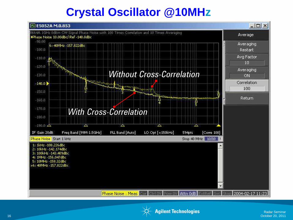
Crystal Oscillator @10MHz
Without Cross-Correlation
With Cross-Correlation
October 20, 2011
Radar Seminar
16

Signal Generators @ 232MHz
October 20, 2011
Radar Seminar
17

“Wide” PN / Heterodyne (digital) discriminator method
Basic theory of operation (for a single channel of the E5052B)
BPF
MIX.
FLL
L.O.
fRF
fLO
fIF Signal Source
Under Test
Scaling amp.
(Frequency Locked Loop)
DSP
(FFT)
t
LPF
PM
noise
Digital Signal Processing
ADC
time
V1(t)
V2(t)
October 20, 2011
Radar Seminar
18

AM noise measurement
Basic theory of operation (for a single channel of the E5052B)
BPF
MIX.
FLL
L.O.
fRF
fLO
fIF Signal Source
Under Test
Scaling amp.
Note that a main signal still exists at this point !
(Frequency Locked Loop)
v
DSP
(FFT)
t
LPF
LPF
AM noise
Digital Signal Processing
ADC
time
V1(t)
V2(t)
October 20, 2011
Radar Seminar
19

“Normal” PN / PLL method (E5053A + E5052B)
Basic theory of operation (for a single channel of E5053A + E5052B)
BPF
MIX.
L.O.1
fRF
fLO1
Signal Source
Under Test fIF
Display
LPF ADC Signal
Processing
(FFT) MIX.
PLL
L.O.2
fLO2 Scaling amp.
(Digital PLL) △p/2 rad
fLO2 = fIF
The phase difference between two signals is kept at 90 deg (p/2 rad) due to PLL operation.
a very stable L.O.
(Frequency down converter)
(E5053A) (E5052B)
IF Gain
October 20, 2011
Radar Seminar
20

October 20, 2011
Radar Seminar
21

October 20, 2011
Radar Seminar
22

October 20, 2011
Radar Seminar
24

October 20, 2011
Radar Seminar
25

Baseband noise measurement
LPF
Baseband
input port
(BNC)
ADC
DC cut off filter (Low/High)
capacitors (1410uF/10uF)
50 Ohm Input Impedance
Basic theory of operation
LPF ADC
IF Gain
IF Gain
splitter
Min. frequency: 1Hz / 1kHz
Max. frequency: 100MHz
DSP
(FFT) 250MHz sampling
“Discharge DC Block Capacitor”
when reconnecting to low-voltage devices.
(DC block capacitor)
Caution!

VCO Freq, Power, DC Current Tester Mode
Measurement Results - 800 MHz Band GSM VCO -
Tester Mode
Frequency Counter
Power Meter
DC Current Meter
October 20, 2011
Radar Seminar
27

PLL Synthesizer Measurement Result - 1.75 GHz Synthesizer -
October 20, 2011
Radar Seminar
28