Embed Size (px)
Citation preview

PEEM and Nanoscience
Dr Anton Tadich
Soft X-ray Beamline
Australian Synchrotron
Email: [email protected]
1
Source: www.sljus.lu.se/staff/anders/peem_pic.html

The Australian Synchrotron
2
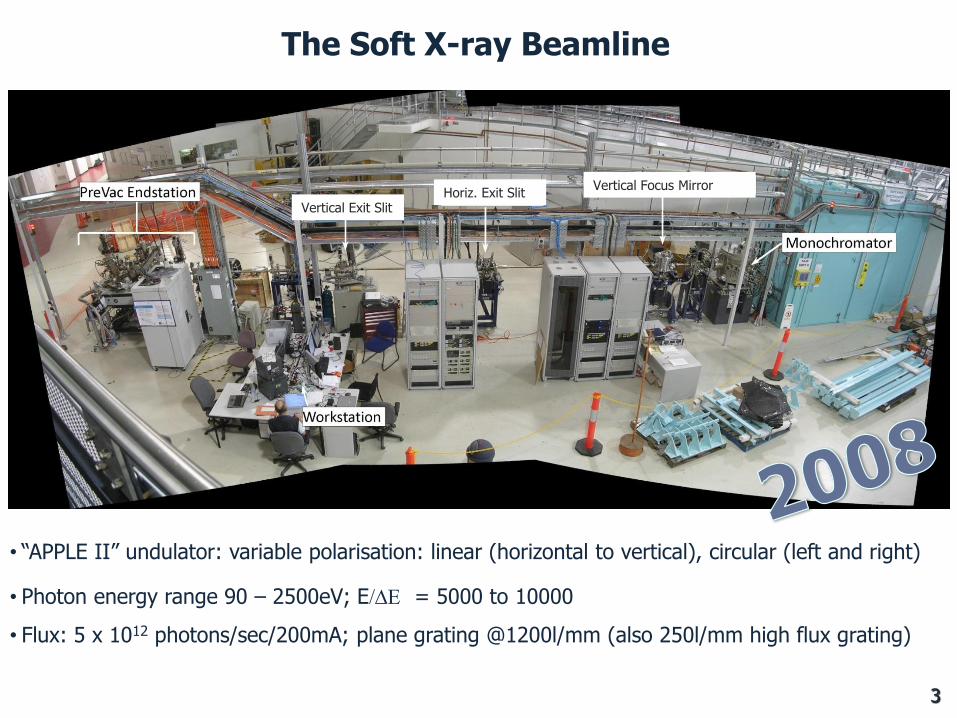
The Soft X-ray Beamline
3
• “APPLE II” undulator: variable polarisation: linear (horizontal to vertical), circular (left and right)
• Photon energy range 90 – 2500eV; E/DE = 5000 to 10000
• Flux: 5 x 10¹² photons/sec/200mA; plane grating @1200l/mm (also 250l/mm high flux grating)
Vertical Exit SlitHoriz. Exit Slit
Vertical Focus Mirror

The Soft X-ray Beamline
• Current endstation features XPS and NEXAFS capabilities (simultaneous AEY, TEY, TFY, PEY)
• Phoibos 150 Hemispherical Analyser
• Sample cleaving, cooling, heating, LEED, K-cells, gas introduction/dosing
• New user hutch, air conditioned!
• PEEM???

The Growth of Nanotechnology
• Nanotechnology represents a rapidly expanding sector of materials technology
• There has been a 279% increase in nanotechnology-based products since 2006
Source: http://www.nanotechproject.org/inventories/consumer/analysis_draft/
• Predicted worldwide turnover of over 1 trillion Euro by 2015.
5

Characterisation at the Nanoscale
• The continual miniaturization of devices and material structures demands novel methods for nanoscale investigations of surfaces, thin films and interfaces
• An understanding of the properties of novel systems benefits greatly from spatially-resolved spectroscopic measurements with “nanometer” resolution
“Real Space” structure (nm and below)
Scanning and Transmission Electron Microscopy (SEM, TEM), Atomic Force Microscopy (AFM), Scanning Tunneling Microscopy (STM), …
Morphology, geometric structure, atomic positions and surface reconstructions
“Chemical” information
X-Ray Absorption Spectroscopy (NEXAFS, EXAFS) Photoelectron Spectroscopy (XPS, UPS) Infrared (IR), NMR, …
Elemental information, chemical environment, adsorbate geometry, bonding configuration, oxidation state, magnetic properties etc..
• There are a number of tools which excel in either spatial or chemical investigations
6

www.physics.ncsu.edu/stxm/NEXAFS.jpg
• NEXAFS and XPS are well established techniques for surface chemical characterisation
http://www.emal.engin.umich.edu/instruments/resources/XPSsurvey.gif
• Traditional instruments integrate spectral information over the photon-illuminated area
• How can we extend these methods to spatially discriminate on the nanoscale?
Image c
ourt
esy
: w
ww
.theoch
em
.kth
.se
7

• Soft X-ray based spectroscopic microscopy using synchrotron radiation is increasingly the main tool for laterally-resolved spectroscopy on the nanoscale
Soft X-ray Microscopy
Images courtesy: www-als.lbl.gov/als/workshops/scidirecthtml/4Magnetic/magnetic.html
Microspectroscopy
Highly focused probe-beam (KB mirror or zone plates)
Sequential detection (x-rays, electrons)
“Large” area probe-beam
Spectromicroscopy
Parallel imaging (electrons)
8
• One can distinguish methods using sequential acquisition (microspectroscopy), and those featuring parallel acquisition (spectromicroscopy)
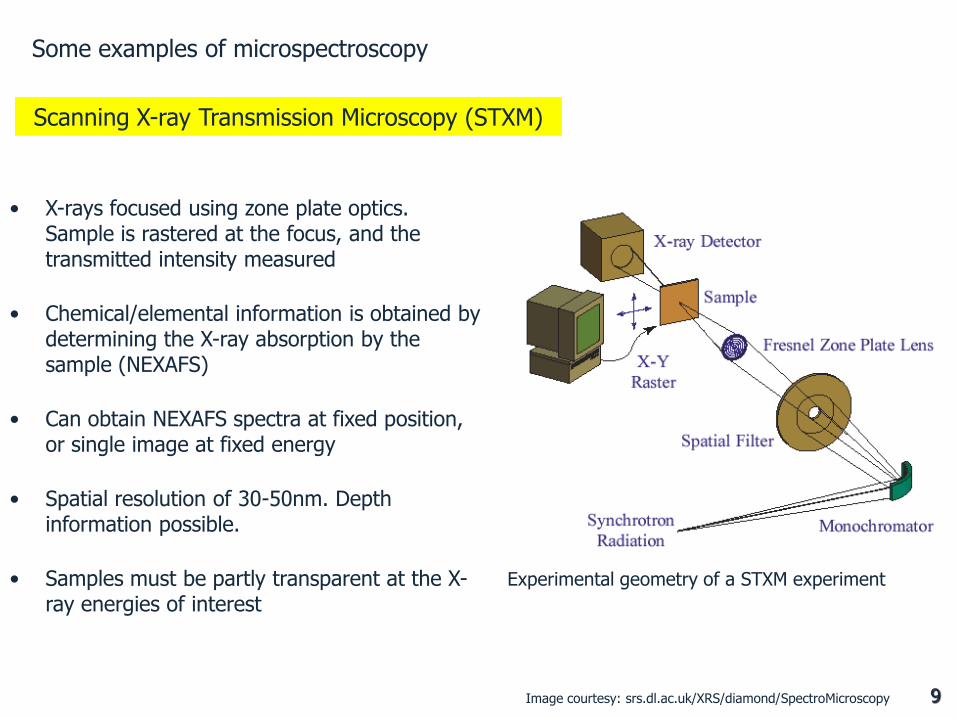
• X-rays focused using zone plate optics. Sample is rastered at the focus, and the transmitted intensity measured
• Chemical/elemental information is obtained by determining the X-ray absorption by the sample (NEXAFS)
• Can obtain NEXAFS spectra at fixed position, or single image at fixed energy
• Spatial resolution of 30-50nm. Depth information possible.
• Samples must be partly transparent at the X-ray energies of interest
Experimental geometry of a STXM experiment
Scanning X-ray Transmission Microscopy (STXM)
Image courtesy: srs.dl.ac.uk/XRS/diamond/SpectroMicroscopy
Some examples of microspectroscopy
9

Scanning photoelectron emission spectroscopy (SPEM)
• High energy resolution is achieved due to well-established spectrometer design
Image co
urte
sy: h
ttp://1
40.1
10.2
03.4
2/sp
em
.htm
Schematic of U5-SPEM instrument, NSRRC.
Scanning Photoemission Microscopy (SPEM)
• A SPEM instrument combines zone plate focussing optics and a conventional electron energy analyzer to perform laterally-resolved photoemission spectroscopy
• Poorer spatial resolution than STXM: combined geometry of illumination and detection yields a resolution of ~ 200nm for modern instruments
10
• The probe is a focussed x-ray beam. The spatial resolution is capped at the diffraction limit of the x-rays
• The focal length of zone plates are a function of x-ray energy: One must displace the sample as the photon energy is changed
• More time consuming than parallel acquisition; time-resolved studies limited
Disadvantages of scanned-mode acquisition
Parallel imaging with photoelectrons: advantages
• Spatial resolution is only limited by aberrations in electron-optical imaging system. Can be improved by design
• Rapid measurement: video rate imaging, time resolved studies (e.g. “pump-probe” experiments)
The most popular type of instrument is the Photo Emission Electron Microscope (PEEM)
11

Basic Principles of PEEM
• In PEEM, the sample is homogeneously illuminated with soft X-rays or ultraviolet (UV) radiation with a spot size ~ field of view of the microscope (1 – 100mm)
• An objective lens operating at high potential (10-30kV) is used to extract the emitted electrons, focussing them to an intermediate image at a back focal plane.
• Projector and transfer optics are used to further magnify the intermediate image onto a 2D detector
Objective
Detector
Transfer/Projector
http://xraysweb.lbl.gov/peem2/webpage/Project/TutorialPEEM.shtml
12

The Photoelectron Energy Distribution
• Photoelectrons exhibit a wide range of energies
Auger Electrons
• Produced via relaxation of the core hole
• Kinetic energy is independent of photon energy.
• Another elemental fingerprint
Core Level Electrons
• Electrons excited from occupied core levels
• Characterized by their binding energy via:
Ekin = hn – EB – f
• Binding energies are element specific
=> elemental fingerprint.
• Peak shape yields chemical states as shifted components etc.
Core Level Peaks
Valence Band
Secondary Electron Tail • Primary peaks (Auger and core level)
are unscattered, and are useful chemical fingerprints (XPS, AES)
• Inelastic scattering of electrons leads to featureless, intense “secondary electron” tail.
Auger
Auger
13

PEEM2 microscope (ALS); a resolution of 20nm can be reached with X-ray energies
PEEM2 (ALS)• The spatial resolution of a PEEM instrument is degraded
by the energy spread of the transmitted electrons (chromatic aberrations)
Images14
Image courtesy: S Anders et al, Rev. Sci. Instr, 70(10) (1999), 3973
• The aperture is typically adjusted enhance the transmission of secondary electrons
• PEEMs contain a contrast aperture to restrict the energy & angular spread of electrons, allowing tradeoff between resolution and transmission
Image courtesy: J Stöhr et. al, IBM J. Res. Develop, 44(4), (2002), p. 535
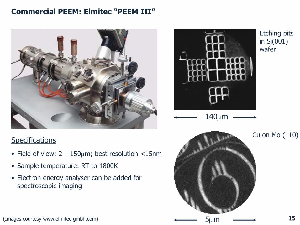
Commercial PEEM: Elmitec “PEEM III”
(Images courtesy www.elmitec-gmbh.com)
Cu on Mo (110)
• Field of view: 2 – 150mm; best resolution <15nm
• Sample temperature: RT to 1800K
• Electron energy analyser can be added for spectroscopic imaging
Specifications
Etching pits in Si(001) wafer
140mm
5mm 15
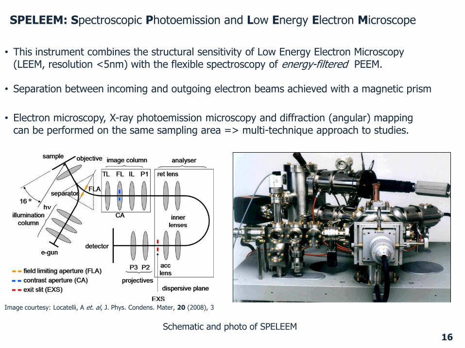
SPELEEM: Spectroscopic Photoemission and Low Energy Electron Microscope
• This instrument combines the structural sensitivity of Low Energy Electron Microscopy (LEEM, resolution <5nm) with the flexible spectroscopy of energy-filtered PEEM.
• Separation between incoming and outgoing electron beams achieved with a magnetic prism
• Electron microscopy, X-ray photoemission microscopy and diffraction (angular) mapping can be performed on the same sampling area => multi-technique approach to studies.
Schematic and photo of SPELEEM16
Image courtesy: Locatelli, A et. al, J. Phys. Condens. Mater, 20 (2008), 3

Elemental and Chemical Contrast
• Monitoring the electron yield at the Auger energy or secondary electron background
=>NEXAFS signal
• Tuning the x-rays through the threshold binding energy will lead to creation of Auger electron (predominant relaxation process for lower Z elements)
• Auger electron scattering contributes to secondary electron signal
Data courtesy A Tadich, L Thomsen, M Gladys, Australian Synchrotron
0
20000
40000
60000
80000
100000
120000
140000
160000
180000
050100150200250
Inte
nsi
ty (a
.u)
Binding Energy (eV)
hn = 320eV
hn = 280eV S2p1/2, 3/2
VB
Cu 3s
Cu 3p1/2, 3/2
C Auger
Cu Auger
S 2s
XPS survey scans below (280eV) and above (320eV) C1s binding energy, for a monolayer of Methionine on Cu(421)
0.6
0.7
0.8
0.9
1
1.1
1.2
1.3
1.4
1.5
280 285 290 295 300 305 310 315 320
Inte
nsi
ty (
a.u
)
hn (eV)
Carbon K-Edge NEXAFS (Auger Electron Yield)
C: 1s -> p*
C: 1s -> s*

• Generation of core holes upon x-ray absorption leads to creation of Auger electrons. Inelastic scattering of the Auger electron contributes to the secondary electron background
Elemental and Chemical Contrast
• Regions of the sample containing that element will appear brighter => element selective contrast. Tuning through several photon energies allows for NEXAFS analysis => chemistry
Tuning to the absorption edge of an element will enhance secondary electron yield for element specific imaging
• The Auger/secondary electron yield is proportional to the x-ray absorption. At an absorption edge, secondary electron intensity will increase. This is a large, accessible signal for PEEM.
Fine structure in the absorption edge (NEXAFS) can be investigated with PEEM, yielding chemical structure
Images courtesy: J Stöhr et. al, IBM J. Res. Develop, 44(4), (2002), p. 535 18

• PEEM image of LaFeO3 thin film, generated by tuning photon energy to the La M5
edge (60s exposure time) 20nm
Data taken from: Scholl, A. Current Opinions in Solid State and Materials Science, 7 (2003), p59
Vertical features are tracks generated by electrical discharge on sample surface
Examples of elemental and chemical imaging
19
• Nickel+photoresist test pattern for PEEM2 project (ALS).
• With photon energy tuned to Nickel L3 edge, nickel areas appear bright
http://xraysweb.lbl.gov/peem2/webpage/Project/TutorialContrast.shtml
• Loss of detail in inner rings at 30nm due to limit of e-beam lithography patterning 100nm spoke width
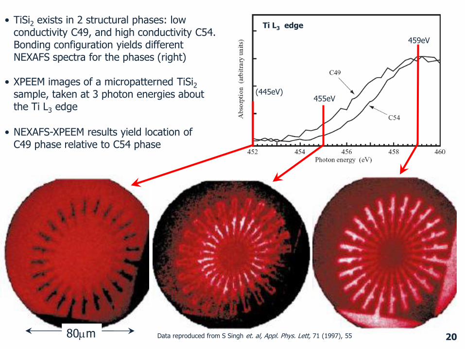
• XPEEM images of a micropatterned TiSi2sample, taken at 3 photon energies about the Ti L3 edge
• TiSi2 exists in 2 structural phases: low conductivity C49, and high conductivity C54. Bonding configuration yields different NEXAFS spectra for the phases (right)
• NEXAFS-XPEEM results yield location of C49 phase relative to C54 phase
Ti L3 edge
459eV
455eV(445eV)
2080mm Data reproduced from S Singh et. al, Appl. Phys. Lett, 71 (1997), 55

Magnetic Contrast
• PEEM is able to resolve ferromagnetic domains, and determine the size and orientation of magnetization vectors, via X-ray Magnetic Circular Dichroism (XMCD)
• Extra contrast in XMCD-PEEM image can obtained by subtracting two images measured at a fixed photon energy, but with opposing helicity vectors
XMCD: The absorption of circularly polarisedlight by ferromagnetic domains depends upon the relative orientation of the domain’s magnetic moment and photon helicity vector
Image courtesy: J Stöhr et. al, IBM J. Res. Develop, 44(4), (2002), p. 535
Data taken from: Engel-Herbert et. al, J. Magn Magn. Mater, 305, p457
XMCD difference-image of ferromagnetic MnAs on GaAs.
Ferromagnetic/paramagnetic striping observed during growth
Black/white areas are opposing ferromagnetic domains. Grey areas are paramagnetic, and show no change upon altering the helicity.
hn
5mm
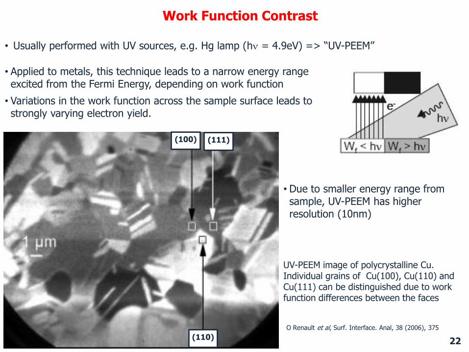
Work Function Contrast
• Usually performed with UV sources, e.g. Hg lamp (hn = 4.9eV) => “UV-PEEM”
UV-PEEM image of polycrystalline Cu. Individual grains of Cu(100), Cu(110) and Cu(111) can be distinguished due to work function differences between the faces
O Renault et al, Surf. Interface. Anal, 38 (2006), 375
(111)(100)
(110)
• Variations in the work function across the sample surface leads to strongly varying electron yield.
• Applied to metals, this technique leads to a narrow energy range excited from the Fermi Energy, depending on work function
22
• Due to smaller energy range from sample, UV-PEEM has higher resolution (10nm)

• For rough samples, the electric field around topographical features is distorted; localised focusing causes contrast in the final image
• Shadowing effects also provide an additional contrast mechanism
Topological Contrast
X-ray PEEM (X-PEEM) of TiO (rutile-phase) nanocrystalsembedded in a TiO (anatase-phase) film. Contrast is due to nanocrystal topography.
Xiong, G et al . Advanced Functional Materials, 17, pp 2133-2138, 2007
m-NEXAFS of nanoparticles and substrate indicates contrast is not due to X-ray absorption (elemental) differences
23

Case Study: Surface Compositional Gradients of InAs/GaAs quantum dots
.
• Energy filtered XPEEM spectra were acquired using SPELEEM at ELETTRA
• Localised photoemission spectra and image maps were obtained to quantitatively determine the lateral In and Ga concentrations
• Measurements on the top down (lateral) distribution and concentration of In were needed
• Understanding of the quantum-confined energy states in self-assembled InxGa(1−x)As/GaAs quantum dots (QD) require an accurate knowledge of the QD shape and composition distribution
• Previous work has obtained QD cross sectional composition using Energy Selective Imaging (ESI) in a TEM
Cross sectional In concentration (x) for InxGa1-xAs QD, obtained by ESI
(Images co
urte
sy: W
alth
er, T
. Phys R
ev Le
tt. 86(1
1) (2
001), p
2381
G Biasiol et. al, Appl. Phys. Lett, 87 (2005) p.223106
24
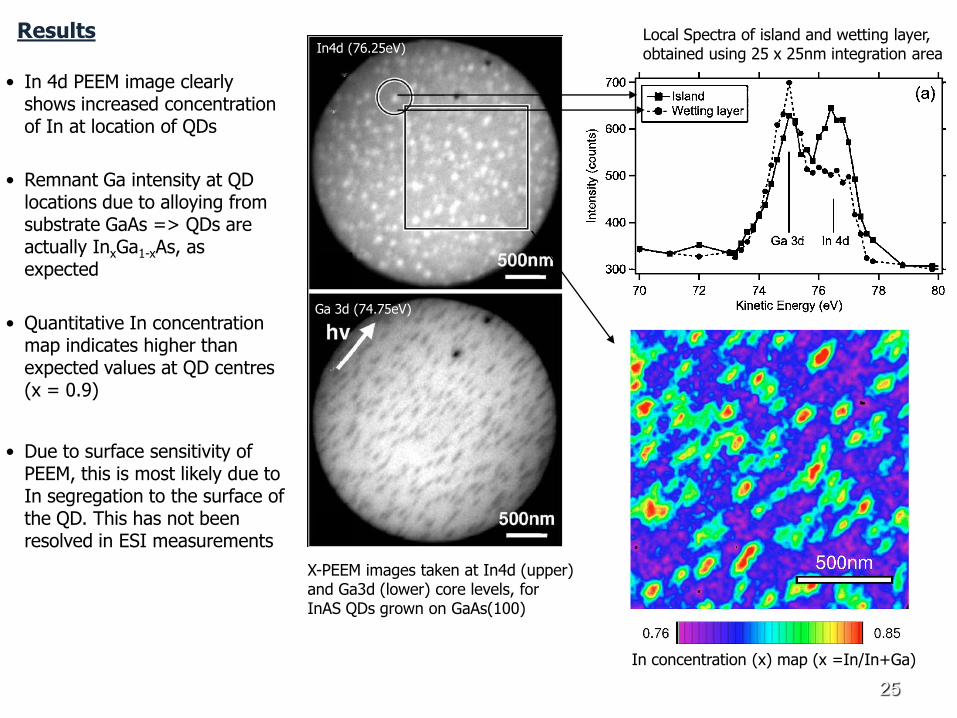
ResultsIn4d (76.25eV)
Ga 3d (74.75eV)
X-PEEM images taken at In4d (upper) and Ga3d (lower) core levels, for InAS QDs grown on GaAs(100)
• In 4d PEEM image clearly shows increased concentration of In at location of QDs
• Remnant Ga intensity at QD locations due to alloying from substrate GaAs => QDs are actually InxGa1-xAs, as expected
Local Spectra of island and wetting layer, obtained using 25 x 25nm integration area
In concentration (x) map (x =In/In+Ga)
• Quantitative In concentration map indicates higher than expected values at QD centres (x = 0.9)
• Due to surface sensitivity of PEEM, this is most likely due to In segregation to the surface of the QD. This has not been resolved in ESI measurements
25

Next Generation PEEM: Pure Aberration Correction
All electron-optical systems exhibit image degradation effects:
Diffraction
Can be reduced by using high electron energy and large apertures
Astigmatism
Caused by mechanical misalignment and tolerances. In a PEEM, corrected using “stigmator” and “deflector” electrodes.
Spherical aberrations
Electrons entering regions of different field curvature will be focussed to different degrees. By limiting the acceptance angle of electrons (the contrast aperture), thus keeping electrons near-axis, aberrations are reduced.
Chromatic aberrations
Caused by the energy spread of electrons. Energy foci are spread along principal axis. Small if the energy range is restricted.
26

22
2
2 cs
d dd
dd
sin
61.0dd
3sinss Cd
sino
ccE
ECd
D
The contribution of each aberration:
Diffraction
Spherical aberrations
Chromatic aberrations
The radius of the disc of confusion from the objective is given by:
Where:
= acceptance angle
= electron wavelength (nm)
E0 = Start Energy (eV)
DE = energy spread (eV)
27

The resolution limit calculated for a typical objective lens:
• For < 20 mrad, resolution is diffraction limited
• For ≈ 20 - 400mrad, resolution is dominated by chromatic aberrations
• For > 400 mrad, resolution is dominated by the spherical aberrations
Figure courtesy of: Th. Schmidt et. al Surface Review and Letters , 9 (2002), no. 1, 223–232.
Notes:
Rapid increase in transmission as a function of
One optimal aperture for best resolution
28
• Clearly, improvement is needed for resolving structures less than 5nm in size!

• Modern TEM and SEM instruments are now corrected for chromatic and spherical aberrations. Progress in LEEM/PEEM has been slower.
• Although the contrast aperture in the back focal plane can be adjusted (reduce ) to reduce the chromatic/spherical aberrations, it is at the expense of transmission
• Majority of the aberrations are caused by the high electric field and focussing in the objective lens
Image: J. Feng, Rev. Sci. Instr, 73, no. 3 (2002), 1514
• For PEEM2, 20nm resolution occurs at 1% transmission! How can we cope with radiation sensitive samples???
• A major effort has been to remove instrinsic aberrations via use of an electron tetrode mirror. Goal is to obtain an order of magnitude in resolution for given transmission.
• 2 projects are heading toward completing an aberration corrected PEEM: the “PEEM3” project at the ALS, and the “SMART” project at BESSY2
Image: Wu, Y.K, Nucl Instr. Methods. Phys. Res. A, 519 (2004), 230 29

Some commercial PEEM instruments• A tetrode electron mirror is able to induce aberrations of the opposite sign to those created in
the objective lens of a PEEM
• Adjustment of the 3 potentials allows correction of a range of aberration coefficients (Cs, Cc ) corresponding to different imaging conditions (E, DE, etc..)
How does an electron mirror correct aberrations?
30
Spherical aberration correction
Chromatic aberration correction
e-

• The (aberrated) image is formed by the objective lens at the entrance to the beam separator
• Reflection occurs in the mirror, with the image then diverted to the exit of the beam separator for subsequent imaging by projection optics
Incorporating the electron mirror: PEEM3
• A magnetic beam separator is used to deflect the electrons into the mirror
Layout of PEEM3, indicating magnetic beam separator and electron tetrode mirror
Image courtesy: J Feng et.al, J. Phys. Condens. Mater, 17, S1339, 2005
31
Design challenge: the separator needs to designed nearly free of aberrations in magnetic field

SMART project
Simulations of resolution gain using the tetrode mirror
32
Image courtesy: Schmidt, Th et.al., Surf. Rev. Lett, 9(1) (2004) 223
PEEM3
Image courtesy: J. Feng et. al, J. Phys. Condes. Matter, 17 (2005) S1339

Design vision of PEEM3 at the ALS
33
Resolution Goals (XPEEM)
• 50nm resolution at a transmission of 100%
• 4nm resolution at a transmission of 1-2%

Progress on PEEM3
34
Sample Manipulator
Mu-metal shielding: 3 layers!
Space for corrector
Electron optics
An intermediate version of the instrument is being commissioned while the separator and corrector are completed offline
Images courtesy: MacDowell A.A e al, Synchrotron Radiation Instrumentation: 9th International Conference (2007), 1341

SMART (Spectro Microscope For All Relevant Techniques): BESSY2
W-filter: energy filtering, dispersive energy plane imaging
35
• The SMART allows for interchange of energy filtered diffraction or real image planes, permitting angular distribution measurements e.g. for k-space mapping, PED, Fermi Surface
LEEM optics

Elmitec are prototyping an aberration corrected LEEM/PEEM: The “AC LEEM/PEEM”
Specifications
• Calculated best resolution <3nm
• Imaging modes: PEEM, LEEM, LEED, MEM….
• Up to 8 times the intensity at a given resolution compared to previous “PEEMIII” (NOT PEEM3)
36

37
Some useful references
J Stohr et. al, IBM. J. Res. Develop, 44(4), 535 (2000)
Anders, S et. al, Review of Scientific Instruments, 70(10), 3973 (1999)
Scholl, A et. al, Current Opinion in Solid State and Materials Science, 7, 69 (2003)
Locatelli, A et. al, Journal of Physics C: Condensed Matter, 20, 1 (2008)
Tonner, B.P et. al, Journal of Electron Spectroscopy and Related Phenomena, 75, 309 (1995)
Schmidt, Th et. al, Surface Review and Letters, 9(1), 223 (2008)
Wu, Y.K et. al, Nuclear Instruments and Methods in Physics Research A, 519, 230 (2004)
Schmid, P et. al, Review of Scientific Instruments, 76, 023302 (2005)
Feng, J et. al, Journal of Physics C: Condensed Matter, 17, S1339 (2005)
Wan, W et. al, Nuclear Instruments and Methods in Physics Research A, 519, 222 (2004)Aberration Correction PEEM3/SMART
Reviews and basics of PEEM