Embed Size (px)
Citation preview

[AK4145]
MS0982-E-01 2010/09 - 1 -
GENERAL DESCRIPTION The AK4145 is a BTSC Encoder with D/A Converter, which is optimized for Digital AV application. The AK4145 achieves high audio performance using a digital BTSC encoding architecture which requires no alignment of external parts. The AK4145 supports major audio data formats (MSB justified, I2S, TDM) to interface with usual DSP. Therefore, the AK4145 is suitable for the systems such as Digital STB/TV, digital recorder.
FEATURES Alignment Free Digital BTSC Stereo Encoding Base band Composite Audio Output (Mono/Stereo) Digital Volume for Composite Audio Output Digital De-emphasis filter (32k/44.1k/48kHz) Stereo Digital Volume Control for Audio Input Data Soft Mute Stereo Matrix Control Sampling Rate (fs): 32k/44.1k/48kHz Master Clock: 256fs/384fs/512fs/768fs I/F format: 24-Bit MSB justified, 24/20/16-Bit LSB justified or I2S Control: Standalone/I2C-bus Selectable Video Input for Pilot Synchronization S/(N+D): 0.01% S/N: 82dB Channel Separation: 47dB Power Supply: 1.7V ~ 1.9V, 2.7 ~ 3.6V Ta: -20 ~ 85°C
LRCK
BICK
SDTI
AudioData
Interface
MCLKPDN
Digital BTSC
Encoder
CA DAC
CV/27M
DVDD
VSS
VCOM
P/S
µPInterface
PLL FS1/SDADIF/SCL
FILT
Sync separator
De-emphasis, DVOL,
Stereo Matrix
AVDD
DATT
TVDD
Digital BTSC Stereo EncoderAK4145

[AK4145]
MS0982-E-01 2010/09 - 2 -
■ Ordering Guide AK4145ET -20 ∼ +85°C 16pinTSSOP
AKD4145 Evaluation Board
■ Pin Layout
1 FILT
PDN
PSN
LRCK
BICK
SDTI
Top View
2
3
4
5
6
7
8
CA
AVDD
VSS
VCOM
DVDD
TVDD
DIF/SCL
FS/SDA
16
15
14
13
12
11
10
9
MCLK
CV27M

[AK4145]
MS0982-E-01 2010/09 - 3 -
PIN/FUNCTION No. Pin Name I/O Function 1 FILT - Filter Pin, 4.7nF must be connected between FILT pin and VSS pin. 2 PSN I Parallel/Serial Select Pin
“L”: Serial control mode, “H”: Parallel control mode 3 CV27M I Composite Video or 27MHz Signal Input Pin. 4 PDN I Power-Down Mode Pin
When at “L”, the AK4145 is in the power-down mode and is held in reset. The AK4145 must be reset once upon power-up.
5 MCLK I Master Clock Input Pin 6 LRCK I Channel Clock Input Pin 7 BICK I Audio Serial Data Clock Input Pin 8 SDTI I Audio Serial Data Input Pin
FS I Sampling Rate Control Pin in parallel control mode 9 SDA I/O Control Data Pin in serial control mode DIF I Audio Data Interface Format Pin in parallel control mode 10 SCL I Control Data Clock Pin in serial control mode
11 TVDD - Digital I/O Power Supply Pin, DVDD(min:1.7V) ∼ 3.6V 12 DVDD - Digital Power Supply Pin, 1.7 ∼ 1.9V 13 VSS - Ground Pin 14 VCOM O Common Voltage Pin, AVDD/2
Normally connected to VSS with a 0.1μF ceramic capacitor in parallel with a 10μF electrolytic cap.
15 AVDD - Analog Power Supply Pin, 2.7 ∼ 3.6V 16 CA O Baseband Composite Audio Output Pin
Note: All input pins should not be left floating. ■ Handling of Unused Pin The unused I/O pins should be processed appropriately as below. Classification Pin Name Setting Analog CV Connect to VSS. Digital FS(Parallel mode), DIF(Parallel mode) Connect to VDD or VSS.
■ Output Status at PDN pin = “L” Below is the output status of each output pin when the PDN pin = “L”. Pin# Pin Name Status 1 FILT VSS 9 SDA Hi-Z 14 VCOM VSS 16 CA VCOM(=VSS)
[AK4145]
MS0982-E-01 2010/09 - 4 -
ABSOLUTE MAXIMUM RATINGS (VSS=0V; Note 1) Parameter Symbol min max Units Power Supply
AVDD DVDD TVDD
-0.3 -0.3 -0.3
4.3 2.4 4.3
V V V
Input Current, Any Pin Except Supply IIN - ±10 mA Analog Input Voltage (CV27M pin) VINA -0.3 AVDD+0.3 V Digital Input Voltage (Note 2) VIND -0.3 TVDD+0.3 V Ambient Temperature (powered applied) Ta -20 85 °C Storage Temperature Tstg -65 150 °C Note 1. All voltages with respect to ground. Note 2. PSN, PDN, MCLK, LRCK, BICK, SDTI, FS/SDA, DIF/SCL pin WARNING: Operation at or beyond these limits may result in permanent damage to the device.
Normal operation is not guaranteed at these extremes.
RECOMMENDED OPERATING CONDITIONS (VSS=0V; Note 1) Parameter Symbol min typ max Units Power Supply
AVDD DVDD TVDD
2.7 1.7
DVDD
3.3 1.8 3.3
3.6 1.9 3.6
V V V
WARNING: AKM assumes no responsibility for the usage beyond the conditions in this datasheet.
[AK4145]
MS0982-E-01 2010/09 - 5 -
ANALOG CHARACTERISTICS (Ta=25°C; AVDD=TVDD=3.3V; DVDD=1.8V; fs=48kHz; BICK=64fs; Signal Frequency=1kHz; 16bit Data; Measurement frequency=50Hz ∼ 13kHz; unless otherwise specified) Parameter min typ max Units Resolution 16 Bits Composite Audio Output Characteristics
Output Voltage 2.2 Vp-p Load Resistance (Note 3) 5 kΩ Load Capacitance 25 pF
BTSC Encoder Characteristics (Note 4) Mono (1kHz, 100%EIM) 0.01 0.3 % S/(N+D)
Stereo (1kHz, 100%EIM. L or R) 0.01 0.3 % Mono (input off) 75 82 dB S/N
(A-weighted) Stereo (input off) 75 82 dB 1kHz 47 dB 20Hz~500Hz 30 dB 500Hz~5kHz 27 dB
Stereo Separation
5kHz~13kHz 23 dB Mono (20~13kHz) -1 1 dB
Frequency response Stereo (20~13kHz) -1 1 dB
Video Sync Input Characteristics Video Input Sync Level 100 mVp-p Video Input Current 2 uA
Power Supplies Power Supply Current Normal Operation (PDN pin = “H”):
AVDD DVDD TVDD AVDD+DVDD+TVDD
Power down mode (PDN pin = “L”): (Note 5) AVDD DVDD TVDD
14 9 1
10 10 10
30
100 100 100
mA mA mA mA
μA μA μA
Note 3. AC-load. Note 4. Received by the Belar TVM230 (BTSC Decoder) and measured by the Audio Precision (System Two). Refer to
the evaluation board manual. Note 5. All digital input pins are held to VSS.

[AK4145]
MS0982-E-01 2010/09 - 6 -
DC CHARACTERISTICS
(Ta=-20∼ 85°C; AVDD=TVDD=1.7~3.6V, DVDD=1.7~1.9V) Parameter Symbol min typ Max UnitsHigh-Level Input Voltage
TVDD < 2.7V TVDD ≥ 2.7V(PSN pin) TVDD ≥ 2.7V(except PSN pin)
Low-Level Input Voltage TVDD < 2.7V TVDD ≥ 2.7V(PSN pin) TVDD ≥ 2.7V(except PSN pin)
VIH VIH VIH
VIL VIL VIL
80%TVDD 80%TVDD 70%TVDD
- - -
- - - - -
- - -
20%TVDD 20%TVDD 30%TVDD
V V V V
V V
Low-Level Output Voltage (SDA pin: Iout= 3mA) VOL - - 0.3 V Input Leakage Current Iin - - ± 10 μA
SWITCHING CHARACTERISTICS (Ta=-20∼ 85°C; AVDD=2.7 ~ 3.6V, TVDD=1.7~3.6V, DVDD=1. 7~1.9V) Parameter Symbol min typ max UnitsMaster Clock Frequency
Duty Cycle fCLK dCLK
8.192 40
36.864060
MHz%
LRCK Frequency Duty Cycle
fs Duty
32 45
48 55
kHz %
Audio Interface Timing BICK Period BICK Pulse Width Low
Pulse Width High BICK rising to LRCK Edge (Note 6) LRCK Edge to BICK rising (Note 6) SDTI Hold Time SDTI Setup Time
tBCK
tBCKL tBCKH tBLR tLRB tSDH tSDS
1/128fs
30 30 20 20 20 20
ns ns ns ns ns ns ns
Control Interface Timing (I2C Bus) SCL Clock Frequency Bus Free Time Between Transmissions Start Condition Hold Time
(prior to first clock pulse) Clock Low Time Clock High Time Setup Time for Repeated Start Condition SDA Hold Time from SCL Falling (Note 7) SDA Setup Time from SCL Rising Rise Time of Both SDA and SCL Lines Fall Time of Both SDA and SCL Lines Setup Time for Stop Condition Pulse Width of Spike Noise Suppressed by Input Filter Capacitive load on bus
fSCL tBUF
tHD:STA
tLOW tHIGH
tSU:STA tHD:DAT tSU:DAT
tR tF
tSU:STO tSP Cb
-
1.3 0.6
1.3 0.6 0.6 0
0.1 - -
0.6 - 0
400
- - - - - - -
0.3 0.3 -
50 400
kHz μs μs
μs μs μs μs μs μs μs μs ns pF
Reset Timing PDN Pulse Width (Note 8)
tPD
150
ns
Note 6. BICK rising edge must not occur at the same time as LRCK edge. Note 7. Data must be held for sufficient time to bridge the 300 ns transition time of SCL. Note 8. The AK4145 can be reset by bringing the PDN pin = “L”. Note 9. I2C-bus is a trademark of NXP B.V.

[AK4145]
MS0982-E-01 2010/09 - 7 -
■ Timing Diagram 1/fCLK
tCLKL
VIH
tCLKH
MCLK VIL
dCLK=tCLKH x fCLK, tCLKL x fCLK
1/fs
VIHLRCK
VIL
tBCK
tBCKL
VIH
tBCKH
BICKVIL
Figure 1. Clock Timing
tLRB
LRCK
VIHBICK
VIL
tSDS
VIHSDTI
VIL
tSDH
VIH
VIL
tBLR
Figure 2. Serial Interface Timing
[AK4145]
MS0982-E-01 2010/09 - 8 -
tHIGH
SCL
SDAVIH
tLOWtBUF
tHD:STA
tR tF
tHD:DAT tSU:DAT tSU:STA
Stop Start Start Stop
tSU:STO
VIL
VIH
VIL
tSP
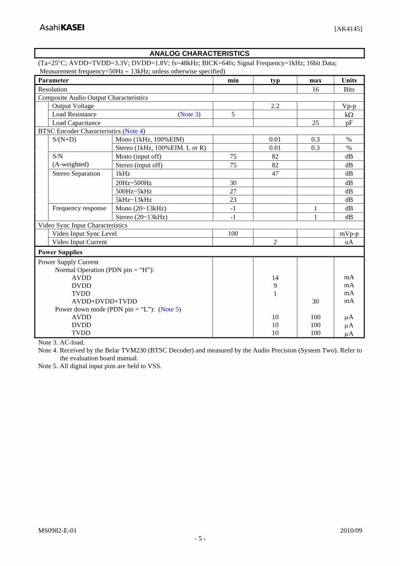
Figure 3. I2C Bus mode Timing
tPD
VILPDN
Figure 4. Power-down Timing
[AK4145]
MS0982-E-01 2010/09 - 9 -
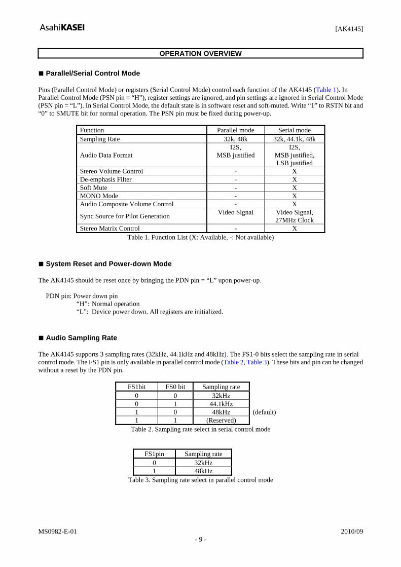
OPERATION OVERVIEW ■ Parallel/Serial Control Mode Pins (Parallel Control Mode) or registers (Serial Control Mode) control each function of the AK4145 (Table 1). In Parallel Control Mode (PSN pin = “H”), register settings are ignored, and pin settings are ignored in Serial Control Mode (PSN pin = “L”). In Serial Control Mode, the default state is in software reset and soft-muted. Write “1” to RSTN bit and “0” to SMUTE bit for normal operation. The PSN pin must be fixed during power-up.
Function Parallel mode Serial mode Sampling Rate 32k, 48k 32k, 44.1k, 48k
Audio Data Format I2S,
MSB justified
I2S, MSB justified, LSB justified
Stereo Volume Control - X De-emphasis Filter - X Soft Mute - X MONO Mode - X Audio Composite Volume Control - X
Sync Source for Pilot Generation Video Signal
Video Signal, 27MHz Clock
Stereo Matrix Control - X Table 1. Function List (X: Available, -: Not available)
■ System Reset and Power-down Mode The AK4145 should be reset once by bringing the PDN pin = “L” upon power-up. PDN pin: Power down pin
“H”: Normal operation “L”: Device power down. All registers are initialized.
■ Audio Sampling Rate The AK4145 supports 3 sampling rates (32kHz, 44.1kHz and 48kHz). The FS1-0 bits select the sampling rate in serial control mode. The FS1 pin is only available in parallel control mode (Table 2, Table 3). These bits and pin can be changed without a reset by the PDN pin.
FS1bit FS0 bit Sampling rate 0 0 32kHz 0 1 44.1kHz 1 0 48kHz (default) 1 1 (Reserved)
Table 2. Sampling rate select in serial control mode
FS1pin Sampling rate 0 32kHz 1 48kHz
Table 3. Sampling rate select in parallel control mode

[AK4145]
MS0982-E-01 2010/09 - 10 -
■ Power-on Sequence After setting the PDN pin “L” to “H”, the AK4145 remains in power-down mode until a LRCK rising edge after MCLK. When the MCLK and LRCK are provided, the AK4145 exits reset state, power-on the voltage reference circuit, and the PLL will be locked. The output signal is masked until when the PLL locks to the MCLK (also RSTN bit = “1” is required in serial mode).
Normal Operat ion
TVDD
(1) Waiting the MCLK&LRCK. PLL=free run (2) PLL Locking Time (3) Data output is Muted
Power off
Power-down state
AVDD
AVDD
PDN (I)
MCLK (I)
(PLL: Internal) (1)
(2)
CA (O)
Power on
(3)
LRCK (I)
(PLL Lock : Internal)
CA=VCOM≅AVDD/2
· · ·
CA=VCOM=VSS
Figure 5. Power-on Sequence
Note:
When changing the sampling rate, the PLL lock signal and BTSC encoder are initialized. The output is muted until the PLL re-locks.
■ System Clock The external clocks required to operate the AK4145 are MCLK, LRCK and BICK. The AK4145 supports 256fs, 384fs, 512fs and 768fs as master clock (MCLK). The AK4145 should be reset by the PDN pin = “L” after these clocks are provided. After exiting reset by the PDN pin = “H”, the AK4145 remains in power-down mode until a LRCK rising edge after MCLK.
MCLK BICK fs 256fs 384fs 512fs 768fs 64fs 128fs
32.0kHz 8.1920MHz 12.2880MHz 16.3840MHz 24.576MHz 2.0480MHz 4.0960MHz44.1kHz 11.2896MHz 16.9344MHz 22.5792MHz 33.8688MHz 2.8224MHz 5.6448MHz48.0kHz 12.2880MHz 18.4320MHz 24.5760MHz 36.8640MHz 3.0720MHz 6.1440MHz
Table 4. System clock example

[AK4145]
MS0982-E-01 2010/09 - 11 -
■ Audio Serial Interface Format Data is shifted in via the SDTI pin using BICK and LRCK inputs. In serial control mode (P/S pin = “L”), the DIF0-2 bits select five serial data modes as shown in Table 5. In parallel control mode (P/S pin = “H”), the DIF pin select two serial data modes as shown in Table 6. In all modes the serial data is MSB-first, 2’s compliment format and it is latched on the rising edge of BICK. Mode 2 can be used for 16/20 MSB justified formats by zeroing the unused LSBs.
Mode DIF2 Bit
DIF1 Bit
DIF0 bit SDTI Format BICK Figure
0 0 0 0 16bit LSB Justified ≥32fs Figure 1 1 0 0 1 20bit LSB Justified ≥40fs Figure 2 2 0 1 0 24bit MSB Justified ≥48fs Figure 3 3 0 1 1 16/24bit I2S Compatible 32fs or ≥48fs Figure 4 (default)4 1 0 0 24bit LSB Justified ≥48fs Figure 2
Table 5. Audio Data Formats (Serial control mode)
Mode DIF pin SDTI Format BICK Figure
2 0 24bit MSB Justified ≥48fs Figure 3 3 1 16/24bit I2S Compatible 32fs or ≥48fs Figure 4
Table 6. Audio Data Formats (Parallel control mode)
SDTI
BICK
LRCK
SDTI 15 14 6 5 4
BICK
0 1 10 11 12 13 14 15 0 1 10 11 12 13 14 15 0 1
3 2 1 0 15 14
(32fs)
(64fs)
0 141 15 16 17 31 0 1 14 15 16 17 31 0 1
15 14 0 15 14 0Mode 0
Don’t care Don’t care
15:MSB, 0:LSB
Mode 015 14 6 5 4 3 2 1 0
Lch Data Rch Data
Figure 1. Mode 0 Timing

[AK4145]
MS0982-E-01 2010/09 - 12 -
SDTI
LRCK
BICK(64fs)
0 91 10 11 12 31 0 1 9 10 11 12 31 0 1
19 0 19 0Mode 1
Don’t care Don’t care
19:MSB, 0:LSB
SDTIMode 4
23:MSB, 0:LSB
20 19 0 20 19 0Don’t care Don’t care22 21 22 21
Lch Data Rch Data
8
23 23
8
Figure 2. Mode 1/4 Timing
LRCK
BICK(64fs)
SDTI
0 221 2 24 31 0 1 31 0 1
23:MSB, 0:LSB
22 1 0 Don’t care23
Lch Data Rch Data
23 30 222 2423 30
22 1 0 Don’t care23 2223
Figure 3. Mode 2 Timing
LRCK
BICK(64fs)
SDTI
0 31 2 24 31 0 1 31 0 1
23:MSB, 0:LSB
22 1 0 Don’t care23
Lch Data Rch Data
23 25 32 2423 25
22 1 0 Don’t care23 23
Figure 4. Mode 3 Timing
[AK4145]
MS0982-E-01 2010/09 - 13 -
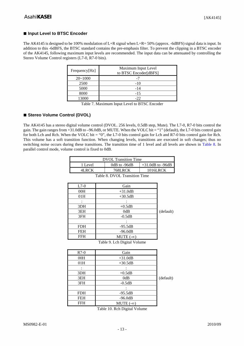
■ Input Level to BTSC Encoder The AK4145 is designed to be 100% modulation of L+R signal when L=R= 50% (approx. -6dBFS) signal data is input. In addition to this -6dBFS, the BTSC standard contains the pre-emphasis filter. To prevent the clipping in a BTSC encoder of the AK4145, following maximum input levels are recommended. The input data can be attenuated by controlling the Stereo Volume Control registers (L7-0, R7-0 bits).
Frequency[Hz] Maximum Input Level to BTSC Encoder[dBFS]
20~1000 -7 2500 -10 5000 -14 8000 -15
13000 -22 Table 7. Maximum Input Level to BTSC Encoder
■ Stereo Volume Control (DVOL) The AK4145 has a stereo digital volume control (DVOL. 256 levels, 0.5dB step, Mute). The L7-0, R7-0 bits control the gain. The gain ranges from +31.0dB to –96.0dB, or MUTE. When the VOLC bit = “1” (default), the L7-0 bits control gain for both Lch and Rch. When the VOLC bit = “0”, the L7-0 bits control gain for Lch and R7-0 bits control gain for Rch. This volume has a soft transition function. When changing levels, transitions are executed in soft changes; thus no switching noise occurs during these transitions. The transition time of 1 level and all levels are shown in Table 8. In parallel control mode, volume control is fixed to 0dB.
DVOL Transition Time 1 Level 0dB to -96dB +31.0dB to -96dB4LRCK 768LRCK 1016LRCK
Table 8. DVOL Transition Time
L7-0 Gain 00H +31.0dB 01H +30.5dB
: : 3DH +0.5dB 3EH 0dB (default) 3FH -0.5dB
: FDH -95.5dB FEH -96.0dB FFH MUTE (-∞)
Table 9. Lch Digital Volume
R7-0 Gain 00H +31.0dB 01H +30.5dB
: : 3DH +0.5dB 3EH 0dB (default) 3FH -0.5dB
: FDH -95.5dB FEH -96.0dB FFH MUTE (-∞)
Table 10. Rch Digital Volume

[AK4145]
MS0982-E-01 2010/09 - 14 -
■ De-emphasis Filter A digital de-emphasis filter is built-in (tc = 50/15µs) for pre-emphasized audio data input. Setting the DEM bit “1” enables the digital de-emphasis filter. In parallel control mode, the de-emphasis filter is always “OFF”
DEM bit De-emphasis Filter 1 ON 0 OFF (default)Table 11. De-emphasis Filter Control
■ Soft Mute Operation When the SMUTE bit is set to “1”, if the volume level was 0dB, the output signal is attenuated to -∞dB in 772 LRCK cycles. When the SMUTE bit returns to “0”, the mute is cancelled and the attenuation gradually changes to the volume level. If the soft mute is cancelled before attenuating to the mute state, the attenuation is discontinued and returned to volume level by the same cycles. The soft mute is effective for changing the signal source without stopping the signal transmission. In parallel control mode, the soft mute function is not available.
Notes:
(1) Transition time. 772 LRCK cycles (772/fs) when the volume level is 0dB. (2) If the soft mute is cancelled before attenuating to -∞, the attenuation is discontinued
and returned to the volume level by the same number of clock cycles.
Figure 6. Soft Mute
SMUTE bit
Volume level
Gain (at the input of encoder block)
-∞dB (1)
(2)
(1)
[AK4145]
MS0982-E-01 2010/09 - 15 -
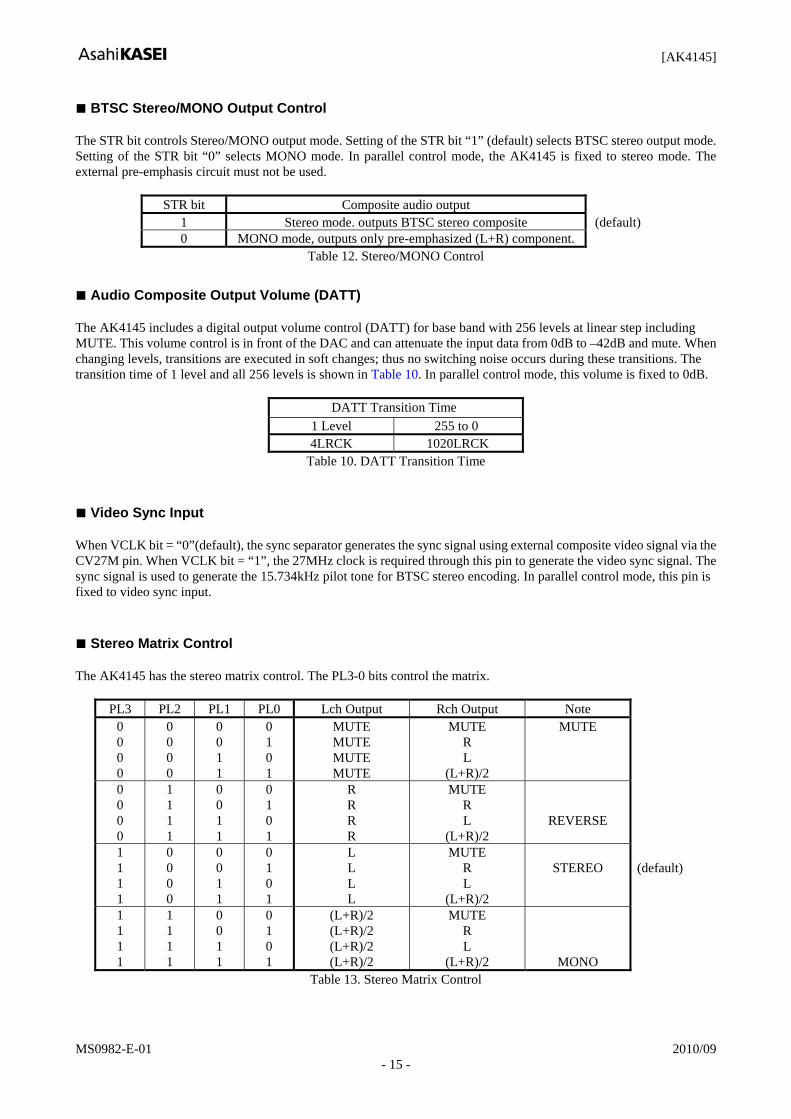
■ BTSC Stereo/MONO Output Control The STR bit controls Stereo/MONO output mode. Setting of the STR bit “1” (default) selects BTSC stereo output mode. Setting of the STR bit “0” selects MONO mode. In parallel control mode, the AK4145 is fixed to stereo mode. The external pre-emphasis circuit must not be used.
STR bit Composite audio output 1 Stereo mode. outputs BTSC stereo composite (default) 0 MONO mode, outputs only pre-emphasized (L+R) component.
Table 12. Stereo/MONO Control ■ Audio Composite Output Volume (DATT) The AK4145 includes a digital output volume control (DATT) for base band with 256 levels at linear step including MUTE. This volume control is in front of the DAC and can attenuate the input data from 0dB to –42dB and mute. When changing levels, transitions are executed in soft changes; thus no switching noise occurs during these transitions. The transition time of 1 level and all 256 levels is shown in Table 10. In parallel control mode, this volume is fixed to 0dB.
DATT Transition Time 1 Level 255 to 0 4LRCK 1020LRCK
Table 10. DATT Transition Time ■ Video Sync Input When VCLK bit = “0”(default), the sync separator generates the sync signal using external composite video signal via the CV27M pin. When VCLK bit = “1”, the 27MHz clock is required through this pin to generate the video sync signal. The sync signal is used to generate the 15.734kHz pilot tone for BTSC stereo encoding. In parallel control mode, this pin is fixed to video sync input. ■ Stereo Matrix Control The AK4145 has the stereo matrix control. The PL3-0 bits control the matrix.
PL3 PL2 PL1 PL0 Lch Output Rch Output Note
0 0 0 0
0 0 0 0
0 0 1 1
0 1 0 1
MUTE MUTE MUTE MUTE
MUTE R L
(L+R)/2
MUTE
0 0 0 0
1 1 1 1
0 0 1 1
0 1 0 1
R R R R
MUTE R L
(L+R)/2
REVERSE
1 1 1 1
0 0 0 0
0 0 1 1
0 1 0 1
L L L L
MUTE R L
(L+R)/2
STEREO
(default)
1 1 1 1
1 1 1 1
0 0 1 1
0 1 0 1
(L+R)/2 (L+R)/2 (L+R)/2 (L+R)/2
MUTE R L
(L+R)/2
MONO
Table 13. Stereo Matrix Control

[AK4145]
MS0982-E-01 2010/09 - 16 -
■ Serial Control Interface The AK4145 supports the fast-mode I2C-bus system (max: 400kHz). 1. Data transfer All commands are preceded by START condition. After the START condition, a slave address is sent. When the AK4145 recognizes START condition, the device interfaced to the bus waits for the slave address to be transmitted over the SDA line. If the transmitted slave address matches an address for one of the devices, the designated slave device (receiver) pulls the SDA line to LOW (ACKNOWLEDGE). The data transfer is always terminated by STOP condition generated by the master device. 1-1. Data validity The data on the SDA line must be stable during the HIGH period of the clock. HIGH or LOW state of the data line can only be changed when the clock signal on the SCL line is LOW except for the START and the STOP condition.
SCL
SDA
DATA LINESTABLE :
DATA VALID
CHANGEOF DATAALLOWED
Figure 7. Data transfer
1-2. START and STOP condition A HIGH to LOW transition on the SDA line while SCL is HIGH indicates START condition. All sequences start from the START condition. A LOW to HIGH transition on the SDA line while SCL is HIGH defines STOP condition. All sequences end by the STOP condition.
SCL
SDA
STOP CONDITIONSTART CONDITION Figure 8. START and STOP conditions

[AK4145]
MS0982-E-01 2010/09 - 17 -
1-3. ACKNOWLEDGE ACKNOWLEDGE is a software convention used to indicate successful data transfers. The device will release the SDA line (HIGH) after transmitting the eight bits. The receiver must pull down the SDA line during the acknowledge clock pulse so that that it remains stable “L” during “H” period of this clock pulse. The AK4145 will generate an acknowledge after each byte is received. In read mode, the slave device, the AK4145 will transmit the eight bits of data, release the SDA line and monitor the line for an acknowledge. If an acknowledge is detected, the slave device will continue transmitting the data. If an acknowledge is not detected, the slave device will terminate further data transmissions and await STOP condition.
SCL FROMMASTER
acknowledge
DATAOUTPUT BYTRANSMITTER
DATAOUTPUT BYRECEIVER
1 98
STARTCONDITION
Clock pulsefor acknowledge
not acknowledge
Figure 9. Acknowledge on the I2C-bus
1-4. FIRST BYTE The first byte, which includes seven bits of slave address and one bit of R/W bit, is sent after the START condition. If the transmitted slave address matches an address for one of the device, the receiver which is addressed pulls down the SDA line. The most significant seven bits of the slave address are fixed as “0010011”. The eighth bit (LSB) of the first byte (R/W bit) defines whether the master requested a write or read condition. A “1” indicates that the read operation is to be executed. A “0” indicates that the write operation is to be executed.
0 0 1 0 0 1 1 R/W
Figure 10. The First Byte
[AK4145]
MS0982-E-01 2010/09 - 18 -
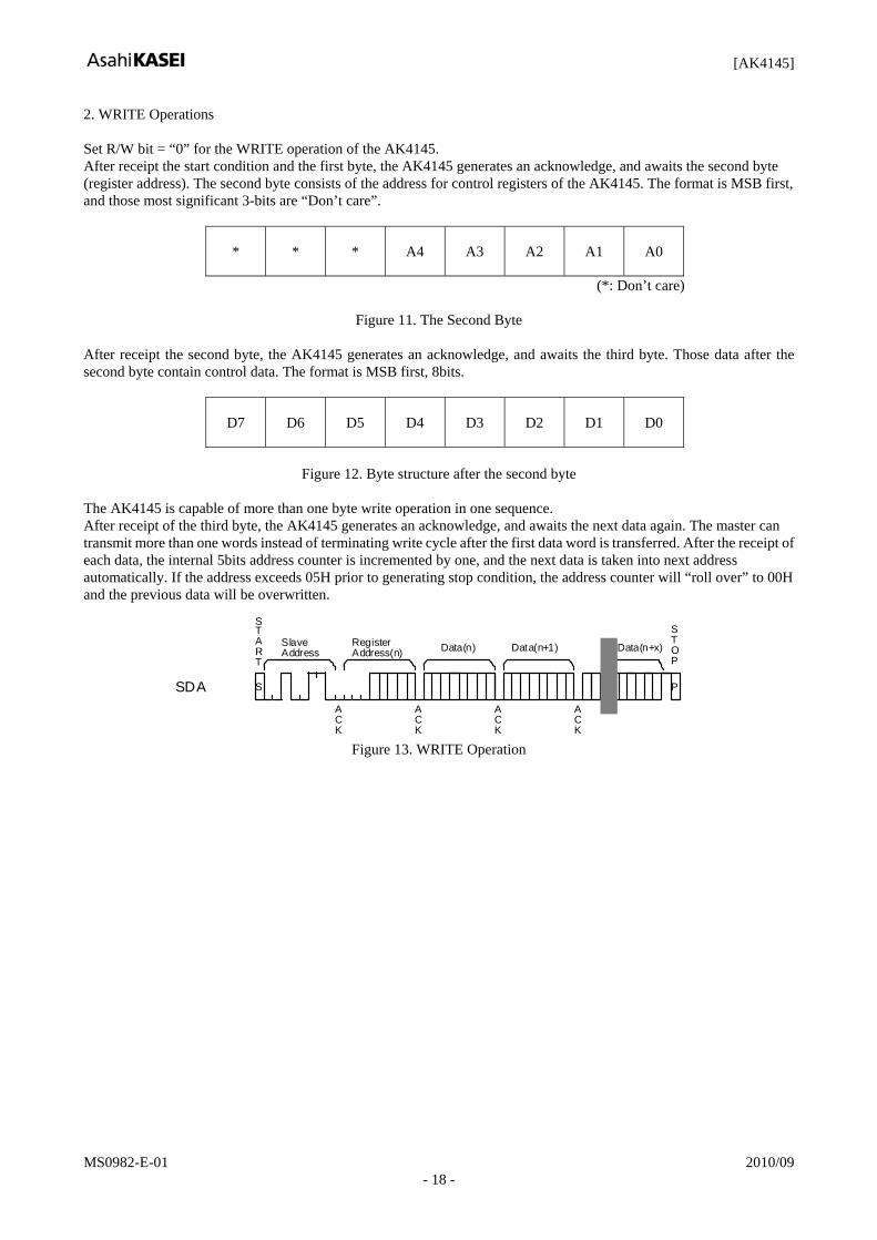
2. WRITE Operations Set R/W bit = “0” for the WRITE operation of the AK4145. After receipt the start condition and the first byte, the AK4145 generates an acknowledge, and awaits the second byte (register address). The second byte consists of the address for control registers of the AK4145. The format is MSB first, and those most significant 3-bits are “Don’t care”.
* * * A4 A3 A2 A1 A0
(*: Don’t care)
Figure 11. The Second Byte After receipt the second byte, the AK4145 generates an acknowledge, and awaits the third byte. Those data after the second byte contain control data. The format is MSB first, 8bits.
D7 D6 D5 D4 D3 D2 D1 D0
Figure 12. Byte structure after the second byte
The AK4145 is capable of more than one byte write operation in one sequence. After receipt of the third byte, the AK4145 generates an acknowledge, and awaits the next data again. The master can transmit more than one words instead of terminating write cycle after the first data word is transferred. After the receipt of each data, the internal 5bits address counter is incremented by one, and the next data is taken into next address automatically. If the address exceeds 05H prior to generating stop condition, the address counter will “roll over” to 00H and the previous data will be overwritten.
SDA
START
ACK
ACK
S
Slave Address
ACK
Register Address(n) Data(n)
P
STOP
Data(n+x)
ACK
Data(n+1)
Figure 13. WRITE Operation
[AK4145]
MS0982-E-01 2010/09 - 19 -
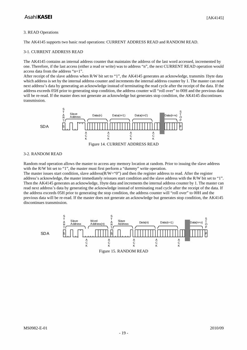
3. READ Operations The AK4145 supports two basic read operations: CURRENT ADDRESS READ and RANDOM READ. 3-1. CURRENT ADDRESS READ The AK4145 contains an internal address counter that maintains the address of the last word accessed, incremented by one. Therefore, if the last access (either a read or write) was to address “n”, the next CURRENT READ operation would access data from the address “n+1”. After receipt of the slave address when R/W bit set to “1”, the AK4145 generates an acknowledge, transmits 1byte data which address is set by the internal address counter and increments the internal address counter by 1. The master can read next address’s data by generating an acknowledge instead of terminating the read cycle after the receipt of the data. If the address exceeds 05H prior to generating stop condition, the address counter will “roll over” to 00H and the previous data will be re-read. If the master does not generate an acknowledge but generates stop condition, the AK4145 discontinues transmission.
SDA
START
ACK
ACK
S
Slave Address
ACK
Data(n) Data(n+1)
P
STOP
Data(n+x)
ACK
Data(n+2)
Figure 14. CURRENT ADDRESS READ
3-2. RANDOM READ Random read operation allows the master to access any memory location at random. Prior to issuing the slave address with the R/W bit set to “1”, the master must first perform a “dummy” write operation. The master issues start condition, slave address(R/W=“0”) and then the register address to read. After the register address’s acknowledge, the master immediately reissues start condition and the slave address with the R/W bit set to “1”. Then the AK4145 generates an acknowledge, 1byte data and increments the internal address counter by 1. The master can read next address’s data by generating the acknowledge instead of terminating read cycle after the receipt of the data. If the address exceeds 05H prior to generating the stop condition, the address counter will “roll over” to 00H and the previous data will be re-read. If the master does not generate an acknowledge but generates stop condition, the AK4145 discontinues transmission.
SDA
START
ACK
ACK
S S
START
Slave Address
Word Address(n)
SlaveAddress
ACK
Data(n)
ACK
P
STOP
Data(n+x)
ACK
Data(n+1)
Figure 15. RANDOM READ

[AK4145]
MS0982-E-01 2010/09 - 20 -
■ Register Map Addr Register Name D7 D6 D5 D4 D3 D2 D1 D0 00H Control 1 VCLK DIF2 DIF1 DIF0 0 0 SMUTE RSTN01H Control 2 VOLC 0 FS1 FS0 0 DEM 0 STR 02H Lch Volume L7 L6 L5 L4 L3 L2 L1 L0 03H Rch Volume R7 R6 R5 R4 R3 R2 R1 R0 04H Composite Volume ATT7 ATT6 ATT5 ATT4 ATT3 ATT2 ATT1 ATT005H Stereo Matrix 0 0 0 0 PL3 PL2 PL1 PL0
Note: For addresses from 06H to 1FH, data must not be written.
When the PDN pin is set to “L”, the registers are initialized to their default values. When the RSTN bit is set to “0”, the internal timing is reset, but registers are not initialized to their default values. Do not write “1” data to the register named “0”.

[AK4145]
MS0982-E-01 2010/09 - 21 -
■ Register Definitions Control 1
Addr Register Name D7 D6 D5 D4 D3 D2 D1 D0 00H Control 1 VCLK DIF2 DIF1 DIF0 0 0 SMUTE RSTN
R/W R/W R/W R/W R/W RD RD R/W R/W Default 0 0 1 1 0 0 1 0
RSTN: Internal timing reset control
0: Reset. Initialize the device except register settings (default). 1: Normal Operation
SMUTE: Soft Mute Control
0: Soft Mute disabled (Normal Operation). 1: Soft Mute enabled (default).
DIF2-0: Audio data interface formats (Table 5)
Default: “011”, I2S
VCLK: Sync Source Control 0: Composite video (default). 1: 27MHz clock
Control 2
Addr Register Name D7 D6 D5 D4 D3 D2 D1 D0 01H Control 2 VOLC 0 FS1 FS0 0 DEM 0 STR
R/W R/W RD R/W R/W RD R/W RD R/W Default 1 0 1 0 0 0 0 1
STR: BTSC Stereo/MONO Output Control
0: MONO 1: BTSC Stereo Composite (default)
DEM: De-emphasis Response
0: Disable (default) 1: Enable
FS1-0: Sampling speed control
00: 32kHz 01: 44.1kHz 10: 48kHz (default) 11: Reserved
VOLC: Lch/Rch Volume Common Control Enable
0: Independent Control. L7-0 and R7-0 bits control Lch and Rch independently. 1: Common Control (default). L7-0 bits control both Lch and Rch. R7-0 bits are ignored.

[AK4145]
MS0982-E-01 2010/09 - 22 -
Lch Volume control
Addr Register Name D7 D6 D5 D4 D3 D2 D1 D0 02H Lch Volume L7 L6 L5 L4 L3 L2 L1 L0
R/W R/W R/W R/W R/W R/W R/W R/W R/W Default 0 0 1 1 1 1 1 0
L7-0: Lch Volume Control when VOLC bit = “0” (Table 9).
These bits control both Lch and Rch volume when VOLC bit = “1”.
Rch Volume control
Addr Register Name D7 D6 D5 D4 D3 D2 D1 D0 03H Rch Volume R7 R6 R5 R4 R3 R2 R1 R0
R/W R/W R/W R/W R/W R/W R/W R/W R/W Default 0 0 1 1 1 1 1 0
R7-0: Rch Volume Control when VOLC bit = “0” (Table 10).
Don’t care when VOLC bit = “1”.
BTSC Composite Volume control
Addr Register Name D7 D6 D5 D4 D3 D2 D1 D0 04H Composite Volume ATT7 ATT6 ATT5 ATT4 ATT3 ATT2 ATT1 ATT0
R/W R/W R/W R/W R/W R/W R/W R/W R/W Default 1 1 1 1 1 1 1 1
ATT = 20 log10 ((ATT_DATA + 1) / 256) [dB]
FFH: 0dB (default) …. 00H: Mute
Stereo Matrix control
Addr Register Name D7 D6 D5 D4 D3 D2 D1 D0 05H Stereo Matrix 0 0 0 0 PL3 PL2 PL1 PL0
R/W RD RD RD RD R/W R/W R/W R/W Default 0 0 0 0 1 0 0 1
PL3-0: Stereo Matrix control
Refer to Table 13.

[AK4145]
MS0982-E-01 2010/09 - 23 -
SYSTEM DESIGN The Figure 16 shows the system connection diagram. The evaluation board (AKD4145) is available for fast evaluation as well as suggestions for peripheral circuitry.
fs
64fs
FILT 1
PSN 2
CV27M 3
PDN 4
MCLK 5
LRCK 6
BICK7
SDTI 8
CA 16
AVDD 15
VCOM 14
VSS 13
DVDD 12
TVDD 11
SCL 10
SDA 9
Master ClockAK4145
Audio Data
Reset & Power down0.1u +
Analog Ground Digital Ground
10u
RF Modulator
Micro Controller
Digital Supply 3.3V
4.7n
Analog Video (CVBS)
0.1u +Analog Supply 3.3V 10u
0.1u Digital Supply 1.8V
0.1u
10u
10k
0.1u
Amp
Figure 16. Typical Connection Diagram

[AK4145]
MS0982-E-01 2010/09 - 24 -
1. Grounding and Power Supply Decoupling The AK4145 requires careful attention to power supply and grounding arrangements. AVDD, DVDD and TVDD are usually supplied from analog supply in system. If AVDD1, AVDD2, DVDD1, DVDD2 and TVDD are supplied separately, the power up sequence is not critical. VSS of the AK4145 must be connected to analog ground plane. System analog ground and digital ground should be connected together near to where the supplies are brought onto the printed circuit board. Decoupling capacitors should be as near to the AK4145 as possible, with the small value ceramic capacitor being the nearest. 2. Voltage Reference Inputs The voltage of AVDD sets the DAC analog output range. VCOM is signal ground of analog output signal. The FILT pin is Loop filter pin for internal PLL. An electrolytic capacitor 10μF parallel with a 0.1μF ceramic capacitor attached between the VCOM pin and VSS pin eliminate the effects of high frequency noise. An 4.7nF capacitor should be attached between the FILTM pin and VSS pin. No load current may be drawn from these VCOM and FILT pins. All signals, especially clocks, should be kept away from the AVDD, VCOM and FILT pins in order to avoid unwanted coupling into the AK4145. 3. Analog Video Input In case of composite video input mode (VCLK bit = “0”), the AK4145 receives the analog video input through the CV27M pin using a 0.1μF ceramic capacitor in series. This video signal is used for the synchronization between the video sync and the pilot frequency on composite audio output. The video input mode is NOT available only when the TVDD is lower than 2.7V. In case of 27MHz clock input mode (VCLK bit = “1”), input the 27MHz clock directly without using a 0.1uF capacitor. 4. Analog Composite Audio Output The analog output is single-ended and centered on around the VCOM voltage. The output signal range scales with the supply voltage and nominally 2.2 x AVDD/3.3 Vpp (@100kHz deviation) at the CA pin. DC offsets on analog outputs are eliminated by AC coupling. The modulation level of sound intermediate frequency (SIF) at RF modulator can be adjusted by the internal composite volume control of the AK4145 (04H D7-0: ATT7-0 bits). The stereo separation can be maximized by tuning the modulation level. If the output level of the AK4145 (typ: 2.2Vpp @100kHz deviation) is not sufficient for the RF modulator device, the external gain stage is used for the extra gain.
22k
Vop
CA10u
RF Modulator
AK4145
0.1u 10u
47k
47k
C (note)
Vop
should be C value should be determine
Note:
The C value must be determined taking account of the input impedance Z at RF modulator. The recommended fc (cut-off frequency) of this high-pass filter is 1Hz or less for low frequency stereo separation. fc = 1/(2 x 3.14 x C x Z). Example: C= 10uF @Z=15kohm, C= 3.3uF @Z=50kohm.
Figure 17. External Gain Stage Example.

[AK4145]
MS0982-E-01 2010/09 - 25 -
PACKAGE
0-10°
Detail A
Seating Plane 0.10
0.17±0.05 0.22±0.1 0.65
*5.0±0.1 1.1 (max)
A
1 8
9 16
16pin TSSOP (Unit: mm)
*4.4
±0.1
6.4±
0.2
0.5±
0.2
0.1±0.1
NOTE: Dimension "*" does not include mold flash.
0.13 M
■ Material & Lead finish
Package molding compound: Epoxy Lead frame material: Cu Lead frame surface treatment: Solder plate (Pb Free)

[AK4145]
MS0982-E-01 2010/09 - 26 -
MARKING
AKM 4145ETXXYYY
1) Pin #1 indication 2) Date Code : XXYYY (5 digits)
XX: Lot# YYY: Date Code
3) Marketing Code : 4145ET 4) Asahi Kasei Logo
REVISION HISTORY
Date (YY/MM/DD) Revision Reason Page Contents 08/08/25 00 First Edition 10/09/17 01 Specification
Change 25 PACKAGE
The package dimension was changed.

[AK4145]
MS0982-E-01 2010/09 - 27 -
IMPORTANT NOTICE
These products and their specifications are subject to change without notice.
When you consider any use or application of these products, please make inquiries the sales office of Asahi Kasei Microdevices Corporation (AKM) or authorized distributors as to current status of the products.
Descriptions of external circuits, application circuits, software and other related information contained in this document are provided only to illustrate the operation and application examples of the semiconductor products. You are fully responsible for the incorporation of these external circuits, application circuits, software and other related information in the design of your equipments. AKM assumes no responsibility for any losses incurred by you or third parties arising from the use of these information herein. AKM assumes no liability for infringement of any patent, intellectual property, or other rights in the application or use of such information contained herein.
Any export of these products, or devices or systems containing them, may require an export license or other official approval under the law and regulations of the country of export pertaining to customs and tariffs, currency exchange, or strategic materials.
AKM products are neither intended nor authorized for use as critical componentsNote1) in any safety, life support, or other hazard related device or systemNote2), and AKM assumes no responsibility for such use, except for the use approved with the express written consent by Representative Director of AKM. As used here:
Note1) A critical component is one whose failure to function or perform may reasonably be expected to result, whether directly or indirectly, in the loss of the safety or effectiveness of the device or system containing it, and which must therefore meet very high standards of performance and reliability. Note2) A hazard related device or system is one designed or intended for life support or maintenance of safety or for applications in medicine, aerospace, nuclear energy, or other fields, in which its failure to function or perform may reasonably be expected to result in loss of life or in significant injury or damage to person or property.
It is the responsibility of the buyer or distributor of AKM products, who distributes, disposes of, or otherwise places the product with a third party, to notify such third party in advance of the above content and conditions, and the buyer or distributor agrees to assume any and all responsibility and liability for and hold AKM harmless from any and all claims arising from the use of said product in the absence of such notification.


![Protective Effect of Coffee Intake on Mortality of French ... · 61 16 1 0.6 [0.3-1.0] 0.060 Having a steady partner § No Yes 399 (38.5) 631 (61.0) 40 37 1 0.6 [0.3-0.9] 0.014 Precarious](https://img.dokumen.tips/doc/110x75/6026e85d2ebf791ed537c7df/protective-effect-of-coffee-intake-on-mortality-of-french-61-16-1-06-03-10.jpg)