Embed Size (px)
Citation preview

Ph: 08040788574 www.rvvlsi.comRVVLSI Confidential
1
Objective
• The objective of this module is to introduce automatic place and route flow & focus on the first phase of this which involves design setup and floor-plan
• After completion of this module you will have a general idea on what make a good floor-plan
• You will have the knowledge to implement a floor-plan at the chip and block level

Ph: 08040788574 www.rvvlsi.comRVVLSI Confidential
2
Prerequisite
• Must have attended the Phase - I of ADAD program.
• Must be aware of commonly used terms and basic ASIC flow and design concepts
• Successfully completed Phase – I demo labs
Ph: 08040788574 www.rvvlsi.comRVVLSI Confidential
3
Agenda
• What is floor-plan and its need
• Understanding the design from a floorplan perspective• Package considerations• Data required for floorplanning• Block and Chip level floorplan• Floor-planning strategies• Power planning

Ph: 08040788574 www.rvvlsi.comRVVLSI Confidential
4
Commonly used terms…
➢Analog PAD➢Antenna effect➢Backend group➢Backup➢Break cell➢CTS➢Congestion➢Contact➢Corner cases➢Corner cell➢Critical net➢Core utilization➢DRC➢DSPF
➢Detail route➢Density(global, local)➢ERC➢ESD➢Electro migration➢Filler➢Foundry➢Frame view➢GDS➢Gate level netlist➢Global route➢G cell➢Hard Macro➢Hierarchy
➢IO ring➢IR Drop➢LUP➢LVS➢Layout➢Layout Porting➢.Lib➢Library group➢Licenses➢Log files➢Low VT➢Low leakage➢Macros➢Masks

Ph: 08040788574 www.rvvlsi.comRVVLSI Confidential
5
➢Metal I➢OPC➢PCells➢P/G PAD➢PDK➢PEX➢PR Boundary➢PSM➢Package➢Pad Opening➢Pitch➢Placement
➢Port Number➢Power & ground domains➢Power routing➢Pin/Port➢Routing➢Rows➢SDF➢SPF➢SDC➢Slotting➢Sheet Resistance➢Soft Macro
➢Spice➢Std cell➢TLR / DR➢Tape out➢Tech files➢Track➢Unit tile
Commonly used terms…

Ph: 08040788574 www.rvvlsi.comRVVLSI Confidential
6
What is a Floor-plan?
• Floor-plan is the physical plan of your chip. Among other things, it defines the size, shape and pin locations of the chip (layout). It also defines the placeable areas for STD cells

Ph: 08040788574 www.rvvlsi.comRVVLSI Confidential
7
Overview of APR Flow
Design & Timing Setup
Floor-planning
Placement
Clock Tree Synthesis
Routing
Design for Manufacturing and Physical Verification
GDSII
Ph: 08040788574 www.rvvlsi.comRVVLSI Confidential
8
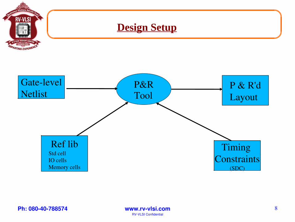
Design Setup
P&R Tool
GatelevelNetlist
Ref libStd cellIO cellsMemory cells
Timing Constraints
(SDC)
P & R'dLayout

Ph: 08040788574 www.rvvlsi.comRVVLSI Confidential
9
Where Does The Netlist Come From?
Logic Synthesis
RTL CodeVerilog/ VHDL
GatelevelNetlist
Constraints

Ph: 08040788574 www.rvvlsi.comRVVLSI Confidential
10
Floor-plan
• Data required before starting– Technology related information– Design data and info– I/O information– Pad or Core limited– Package type

Ph: 08040788574 www.rvvlsi.comRVVLSI Confidential
11
Technology related information
• Techfiles
• .libs• Backend views• Physical verification decks• PEX models• E-specs

Ph: 08040788574 www.rvvlsi.comRVVLSI Confidential
12
Design data
• Logic clusters which are critical or high speed
• Target Die size in area and/or Aspect ratio• Gate count• W.C. Power drop• Package Info• Block diagram and pin information
Ph: 08040788574 www.rvvlsi.comRVVLSI Confidential
13
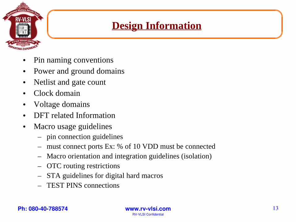
Design Information
• Pin naming conventions
• Power and ground domains• Netlist and gate count• Clock domain• Voltage domains• DFT related Information• Macro usage guidelines
– pin connection guidelines– must connect ports Ex: % of 10 VDD must be connected– Macro orientation and integration guidelines (isolation)– OTC routing restrictions– STA guidelines for digital hard macros– TEST PINS connections
Ph: 08040788574 www.rvvlsi.comRVVLSI Confidential
14
I/O Information
• I/O placement information
• Pin placement information (if block level)• I/O Bus Architecture details

Ph: 08040788574 www.rvvlsi.comRVVLSI Confidential
15
Anatomy of a typical I/O
PAD/CUP/BOA
O/P BuffersPower Bus
I/P Levelshifter
Wire bond side
Core Side

Ph: 08040788574 www.rvvlsi.comRVVLSI Confidential
16
IO power bus architecture
• IO ring– Ordered placement of signal and power IOs and architecture cells that meets design
goals for functionality, power and package
• IO cells have in built power buses that allow propagation of power across IO ring• Libraries normally support more than one power bus architectures to support
multiple needs– A core limited design would need wide and short IOs for achieving optimal die size– An IO limited design would need thin tall IOs for achieving optimal die size
• IO cells can also have circuitry needed for ESD protection• Power hookup

Ph: 08040788574 www.rvvlsi.comRVVLSI Confidential
17
IO bus architecture
• VDD: primary power: 1.2 V
• VSS: primary ground: 0.0 V
• VDDS: secondary power: 3.3 V
• VDDANALOG: Analog power: 3.3 V
VDD
VSS
ESD2Circuit for ESD protection
VDDS
Circuit for IO operation
A typical IO cell with power buses
Port for die external connection
Port for dieinternal connection
VDD
VSS
ESD2Circuit for ESD protection
VDDS
VDDANALOG
Architecture 1 Architecture 2

Ph: 08040788574 www.rvvlsi.comRVVLSI Confidential
18
Bus Transition Cells
• Bus transition cell– This cell helps to keeps
the power bus continuity between IO cells of differing architecture
ESD2Circuit for ESD protection ESD2Circuit for
ESD protection
Bus transition cell

Ph: 08040788574 www.rvvlsi.comRVVLSI Confidential
19
Power break cell
VSS
VDD
ESD2Circuit for ESD protection ESD2Circuit for
ESD protection
VDDS1
VDDANA
VSS
VDD
VDDS2
VDDANA
VSS
VDD
ESD2Circuit for ESD protection
VDDS1
VDDANA
ESD2Circuit for ESD protection
VSS
VDD
VDDS2
VDDANA
VDDS1: 3.3VVDDS2: 2.5V

Ph: 08040788574 www.rvvlsi.comRVVLSI Confidential
20
IO Ring
• Power bus continuity happens just by placing IO cells abutting to each other
• Some of the IO cells act as power sources. They get power (eg: VDD) from outside the die to IO ring as well as die core (place where standard cells are placed) area
A typical die with IO ringand core
IO cells
Power bus
Core
Corner cell

Ph: 08040788574 www.rvvlsi.comRVVLSI Confidential
21
• IO ring consists of following type of cells– IO cell: Can be of type
• Input: This cell helps in bringing the signal into the die from a source external to the die
• Output: This cell helps to send out signals out of the die• Bi-Di: This cell does either Input/Output functionality based on the setting on the on
the cell control signals– Power cell: These cells help to bring power onto the die for consumption by IO
and logic gates – Architecture cells: These cells help in keeping the busses in IO ring continuous
as needed• Corner cells: These cells help to keep the power bus continuous at the corner of the
IO ring• Bus transition cell: These cells help to keep the required power busses between IO
cells of different architecture• Power break cell: These cells help to cut the power busses when needed. For
example, portion of IO ring runs on a different power supply but we have limited number of power buses in the IO ring.
IO Ring

Ph: 08040788574 www.rvvlsi.comRVVLSI Confidential
22
A Core-Limited Die
• The core logic determines the die size.

Ph: 08040788574 www.rvvlsi.comRVVLSI Confidential
23
Pad Limited Die
• The number of pads determines the die size

Ph: 08040788574 www.rvvlsi.comRVVLSI Confidential
24
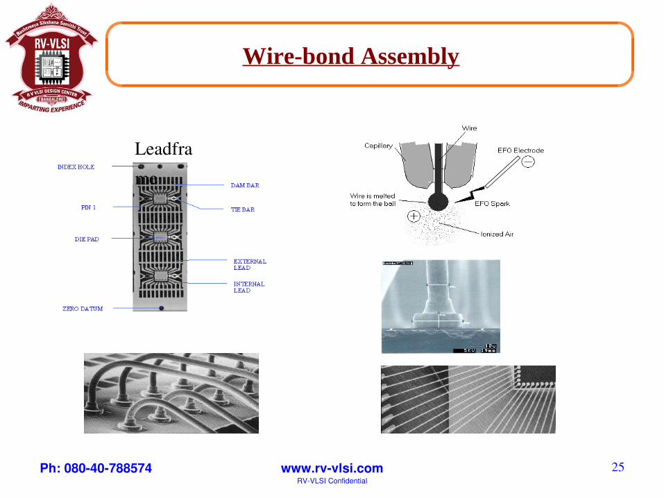
Package
• Wire bond– Types
• Bonding type• Cavity up/down
– Package structure• Package body• Lead frame• Landing • Power plane
PBGA
Cavity Down BGA
➔Why is this important for floorplan?
Ph: 08040788574 www.rvvlsi.comRVVLSI Confidential
25
Wire-bond Assembly
Leadframe

Ph: 08040788574 www.rvvlsi.comRVVLSI Confidential
26
Flip-chip
DieSolder bumps
SubstrateBGA
Bumps attached to the die
• Flip chip– Package structure
•Package body•Bump•Power plane

Ph: 08040788574 www.rvvlsi.comRVVLSI Confidential
27
Bonding Types
Staggered Bonding Inline Bonding
➔Why is this important for floorplan?

Ph: 08040788574 www.rvvlsi.comRVVLSI Confidential
28
IO to Package pin mapping
IO Pad Target
Pad Wire
Bump Pad Trace
Solder Bump
Pin
IO Pad Target
Bond wire
LandingTrace Pin
Flip Chip
Wirebond
Package
Bondpad

Ph: 08040788574 www.rvvlsi.comRVVLSI Confidential
29
Flip-chip
• Advantages– Can get better power distribution than wire-bonds– Higher pin count– Higher frequency
• Disadvantages– Expensive

Ph: 08040788574 www.rvvlsi.comRVVLSI Confidential
30
Power Planning
• Typical specification 5% (For WB)
(VDD) 2.5% (VSS) 2.5%
- 1 % for core ring - 1 % for core strap - 0.5% for row
Will WB handle 2% spec., say

Ph: 08040788574 www.rvvlsi.comRVVLSI Confidential
31
• Two parameters need to be computed– No. of straps– Width of Straps
• Power Planning is an art– Lot of experience – Hard data from past experience– Assume equipotential regions
Power Planning

Ph: 08040788574 www.rvvlsi.comRVVLSI Confidential
32
Overview of APR Flow
Design & Timing Setup
Floor-planning
Placement
Clock Tree Synthesis
Routing
Design for Manufacturing and Physical Verification
GDSII

Ph: 08040788574 www.rvvlsi.comRVVLSI Confidential
33
Why do this step ?
• Create your starting cell

Ph: 08040788574 www.rvvlsi.comRVVLSI Confidential
34
Data in for Floor-plan (Design Setup)
Design library to be builtNetlist from Synthesis
Technology file
Reference libraries for Std cells, I/O cells, Memories
Preserving Hierarchy

Ph: 08040788574 www.rvvlsi.comRVVLSI Confidential
35
The layout is Flat – The Netlist is Not!?
RAM
C1
B
CA3A2A1
A
TOP
C2 C3
RAM
A2 C1
C3
A3C2
A1
TOP
Netlist hierarchical Layout view FLAT

Ph: 08040788574 www.rvvlsi.comRVVLSI Confidential
36
Design Setup
• Load TLU+ model

Ph: 08040788574 www.rvvlsi.comRVVLSI Confidential
37
Design Setup

Ph: 08040788574 www.rvvlsi.comRVVLSI Confidential
38
Design & Timing Setup
Floor-planning
Placement
Clock Tree Synthesis
Routing
Design for Manufacturing and Physical Verification
GDSII
Overview of APR Flow

Ph: 08040788574 www.rvvlsi.comRVVLSI Confidential
39
Chip Level Floor-plan Flow
Create Pad Area
Create Core Area
Place Macros
Create P/G Grid
Add Placement Blockages and
RouteGuides
Create/Assign IO Pads (load .tdf)
Initialize Floorplan
Insert Pad Fillers(axgAddPadFiller)
Connect Pad P/G(aprPGConnect)
Add P/G Rings(axgCreatePad
Continue to floorplan the core area
N
Placement
To CTS
Detach Scan Chains
Timingok?
Y
N Additional Optimizati
ons
AutoPlace
Congestionok?
Y
Set placement common options/ timing

Ph: 08040788574 www.rvvlsi.comRVVLSI Confidential
40
Steps in Floor-plan
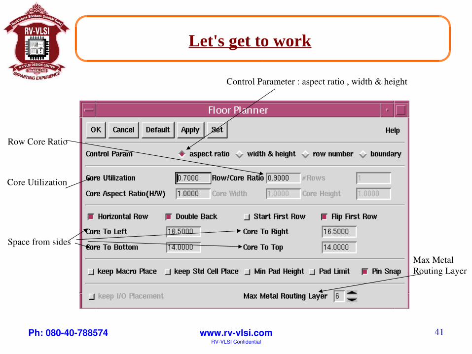
• Implement a given floor-plan, this includes– Defining the core area– Creating and placing power pads– Placing the IO pads and macros– Modifying the orientation of macros– Implement a P/G grid according to given parameters– Defining placement and routing blockages
Ph: 08040788574 www.rvvlsi.comRVVLSI Confidential
41
Let's get to work
Control Parameter : aspect ratio , width & height
Core Utilization
Row Core Ratio
Space from sides
Max Metal Routing Layer

Ph: 08040788574 www.rvvlsi.comRVVLSI Confidential
42
Which control parameter to start with ?
• New design or Existing design?• Understanding the design.• What matters?
– Area – Power– Timing

Ph: 08040788574 www.rvvlsi.comRVVLSI Confidential
43
Core Utilization
(Total Standard Cell + Macro Cell Area) x 100
Core AreaUtilization =
• Core “utilization” is the percentage of the core that is used by placed standard cells and macros.
• Ideally would like to achieve 100% utilization at tape-out. In practice range is 80-85%.
• Recommended starting netlist utilization should not exceed 60-75% to allow for logic optimizations and DFM

Ph: 08040788574 www.rvvlsi.comRVVLSI Confidential
44
Floor-plan Strategies
• Placing I/O– Auto placement– Manual placement– Loading TDF file

Ph: 08040788574 www.rvvlsi.comRVVLSI Confidential
45
Macro placement guidelines
• All memory blocks which are talking to each other must be placed together
• Macro stacking should be limited.– Pins of the macros should be accessible
• Orientation of the macros• Contiguous core area• Is OTC allowed

Ph: 08040788574 www.rvvlsi.comRVVLSI Confidential
46
Macro Placement
• Bad practices– Stacking the macros
See the Congestion See the Congestion

Ph: 08040788574 www.rvvlsi.comRVVLSI Confidential
47
• Manual Placement of Macros with the help of Fly lines
Macro Placement

Ph: 08040788574 www.rvvlsi.comRVVLSI Confidential
48
• Macros Orientation
Macro Placement

Ph: 08040788574 www.rvvlsi.comRVVLSI Confidential
49
Guidelines for a Good Floor-plan
Ph: 08040788574 www.rvvlsi.comRVVLSI Confidential
50
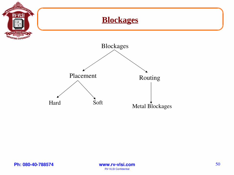
Blockages
Blockages
Placement Routing
Hard Soft Metal Blockages

Ph: 08040788574 www.rvvlsi.comRVVLSI Confidential
51
Important parameters to monitor
• Overflow
• Congestion• Query design utilization

Ph: 08040788574 www.rvvlsi.comRVVLSI Confidential
52
Evaluation of Floor-planning
• A through away placement
• Estimate global route congestion

Ph: 08040788574 www.rvvlsi.comRVVLSI Confidential
53
Analysis of your Floor-plan
• Definition of Congestion Routing demand = 3Assume routing supply is 1,overflow = 3 1 = 2 on this edge.
Overflow = overflowΣall edges
Overflow on each edge = Routing Demand Routing Supply (if Routing Demand > Routing Supply)0 (otherwise)

Ph: 08040788574 www.rvvlsi.comRVVLSI Confidential
54
Analysing congestion: 1-D map
Vertical routing
Horizontal routing
0.48
0.57
0.49
0.53
Average congestion as a percentage of all routing resources across the vertical
plane

Ph: 08040788574 www.rvvlsi.comRVVLSI Confidential
55
Colors represent overflowof demand vs. supply
Analysing congestion: 2-D map

Ph: 08040788574 www.rvvlsi.comRVVLSI Confidential
56
Overflow
• Example:– H routing overflow = 7.6 %– V routing overflow = 15.7 %– Both directions = 23.3 %
Ph: 08040788574 www.rvvlsi.comRVVLSI Confidential
57
Power Calculation
• Which metal layers used?
• Width of the ring and straps?• Number of straps?• Inputs for power calculation?• Chip level and block level power planning?
Ph: 08040788574 www.rvvlsi.comRVVLSI Confidential
58
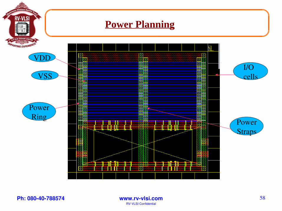
VDD
VSSI/O cells
PowerRing Power
Straps
Power Planning

Ph: 08040788574 www.rvvlsi.comRVVLSI Confidential
59
Power Ring

Ph: 08040788574 www.rvvlsi.comRVVLSI Confidential
60
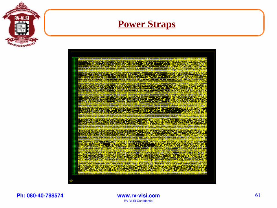
Power Straps
Direction & Start
Net Names : VDD, VSS
width & Layer
Ph: 08040788574 www.rvvlsi.comRVVLSI Confidential
61
Power Straps

Ph: 08040788574 www.rvvlsi.comRVVLSI Confidential
62
Power Straps

Ph: 08040788574 www.rvvlsi.comRVVLSI Confidential
63
Power Straps

Ph: 08040788574 www.rvvlsi.comRVVLSI Confidential
64
Block level Floor-plan
• Core Utilization
• Aspect Ratio• Shape of the Blocks• Pin Locations• Design with different numbers of metal layers.
Ph: 08040788574 www.rvvlsi.comRVVLSI Confidential
65
Module Takeaway
• After completing this module you must have an exposure to the various parameters used to create floor-plan and analysis the quality of the floorplan with your end goals in mind.

Ph: 08040788574 www.rvvlsi.comRVVLSI Confidential
66
References
• Algorithms for VLSI Physical Design Automation by Naveed A. Sherwani.
• https://solvnet.synopsys.com• From Basics to ASICs by Harry Veendrick

Ph: 08040788574 www.rvvlsi.comRVVLSI Confidential
67
Backup

Ph: 08040788574 www.rvvlsi.comRVVLSI Confidential
68
Floorplan
• Aspect Ratio :
1.5
A B C
D E F
2
A B C
D E F
1.75
1.75
A
B C
D
E
F
1.75
1.75

Ph: 08040788574 www.rvvlsi.comRVVLSI Confidential
69
• TDF Format insertPad net Name padCellName padName connectPin netName Name of the net to which the pad should be connected. The net has
Floorplan

Ph: 08040788574 www.rvvlsi.comRVVLSI Confidential
70
Tradeoff of APR
• Not route Efficient• Fast• Timing wise not the Best

Ph: 08040788574 www.rvvlsi.comRVVLSI Confidential
71
Flylines

Ph: 08040788574 www.rvvlsi.comRVVLSI Confidential
72
Macro cells
Pad cells
Chipoutline
Unplacedstandard cells

Ph: 08040788574 www.rvvlsi.comRVVLSI Confidential
73
What is a Standard Cell Library?
• A Standard Cell is a predesigned layout of one specific basic logic gate.
• Each cell usually has the same standard height.• A Standard Cell Library contains a varied collection of standard
cells.• Libraries are usually supplied by an ASIC vendor or library group.

Ph: 08040788574 www.rvvlsi.comRVVLSI Confidential
74
Slicing floor plan
• It is a floor plan which can be obtained by recursively partitioning a rectangle into two parts either by a vertical line or a horizontal line.
• A slicing tree is a binary tree in which each leaf represents a partion and each internal node represents a cut.
EA
B
C
D
H
F GE
I
6 1 7
5 4
3
28

Ph: 08040788574 www.rvvlsi.comRVVLSI Confidential
75
Slicing floor plan
• Slicing tree for the floor plan .1
2 3
4 7 5 6
F G H I D E
B C
8

Ph: 08040788574 www.rvvlsi.comRVVLSI Confidential
76
Slicing floor plan
• Slicing tree indicating the cutdirection.v
H H
V
H
F G H I D E
B C
8
V V V

Ph: 08040788574 www.rvvlsi.comRVVLSI Confidential
77
NonSlicing floor plan
AD
CB
12
34
One that may not be obtained by repetitively subdividing alone.

Ph: 08040788574 www.rvvlsi.comRVVLSI Confidential
78
Macro Placement
• Orientation of the Macros (design dependent)
Macro
Avoid many pins in the narrow channel.Rotate for pin accessibilty.

Ph: 08040788574 www.rvvlsi.comRVVLSI Confidential
79
Add a graph asics to basics page 455