Embed Size (px)
Citation preview

PCA9546A
Slaves A0, A1...AN
Slaves B0, B1...BN
Slaves C0, C1...CN
Slaves D0, D1...DN
I2C or SMBus
Master
(e.g. Processor)
SDA
SCL
SD0
SC0
Channel 0
Channel 1
Channel 2
Channel 3
RESET SD1
SC1
SD2
SC2
SD3
SC3
VCC
A1
A2
GND
A0
Copyright © 2016, Texas Instruments Incorporated
Product
Folder
Sample &Buy
Technical
Documents
Tools &
Software
Support &Community
An IMPORTANT NOTICE at the end of this data sheet addresses availability, warranty, changes, use in safety-critical applications,intellectual property matters and other important disclaimers. PRODUCTION DATA.
PCA9546ASCPS148G –OCTOBER 2005–REVISED MAY 2016
PCA9546A Low Voltage 4-Channel I2C and SMBus Switch with Reset Function
1
1 Features1• 1-of-4 Bidirectional Translating Switches• I2C Bus and SMBus Compatible• Active-Low Reset Input• Three Address Pins, Allowing up to Eight
PCA9546A Devices on the I2C Bus• Channel Selection Via I2C Bus, in Any
Combination• Power-up With All Switch Channels Deselected• Low RON Switches• Allows Voltage-Level Translation Between
1.8-V, 2.5-V, 3.3-V, and 5-V Buses• No Glitch on Power-up• Supports Hot Insertion• Low Standby Current• Operating Power-Supply Voltage Range of 2.3 V
to 5.5 V• 5.5 V Tolerant Inputs• 0 to 400-kHz Clock Frequency• Latch-Up Performance Exceeds 100 mA Per
JESD 78• ESD Protection Exceeds JESD 22
– 2000-V Human-Body Model (A114-A)– 1000-V Charged-Device Model (C101)
(1) For all available packages, see the orderable addendum atthe end of the datasheet.
2 Applications• Servers• Routers (Telecom Switching Equipment)• Factory Automation• Products With I2C Slave Address Conflicts
(for example. Multiple, Identical Temp Sensors)
3 DescriptionThe PCA9546A is a quad bidirectional translatingswitch controlled via the I2C bus. The SCL/SDAupstream pair fans out to four downstream pairs, orchannels. Any individual SCn/SDn channel orcombination of channels can be selected, determinedby the contents of the programmable control register.
An active-low reset (RESET) input allows thePCA9546A to recover from a situation in which one ofthe downstream I2C buses is stuck in a low state.Pulling RESET low resets the I2C state machine andcauses all the channels to be deselected, as does theinternal power-on reset function.
The pass gates of the switches are constructed suchthat the VCC pin can be used to limit the maximumhigh voltage, which will be passed by the PCA9546A.This allows the use of different bus voltages on eachpair, so that 1.8-V, 2.5-V, or 3.3-V parts cancommunicate with 5-V parts without any additionalprotection. External pull-up resistors pull the bus upto the desired voltage level for each channel. All I/Opins are 5.5-V tolerant.
Device Information (1)
PART NUMBER PACKAGE BODY SIZE (NOM)PCA9546A TSSOP (16) 5.00 mm x 4.40 mm
Simplified Application Diagram

2
PCA9546ASCPS148G –OCTOBER 2005–REVISED MAY 2016 www.ti.com
Product Folder Links: PCA9546A
Submit Documentation Feedback Copyright © 2005–2016, Texas Instruments Incorporated
Table of Contents1 Features .................................................................. 12 Applications ........................................................... 13 Description ............................................................. 14 Revision History..................................................... 25 Pin Configuration and Functions ......................... 36 Specifications......................................................... 4
6.1 Absolute Maximum Ratings ..................................... 46.2 ESD Ratings ............................................................ 46.3 Recommended Operating Conditions ...................... 46.4 Electrical Characteristics........................................... 56.5 I2C Interface Timing Requirements.......................... 56.6 Interrupt and Reset Timing Requirements ................ 76.7 Switching Characteristics .......................................... 7
7 Parameter Measurement Information .................. 88 Detailed Description ............................................ 10
8.1 Overview ................................................................. 108.2 Functional Block Diagram ....................................... 10
8.3 Feature Description................................................. 118.4 Device Functional Modes........................................ 118.5 Programming........................................................... 118.6 Control Register ...................................................... 14
9 Application and Implementation ........................ 159.1 Application Information............................................ 159.2 Typical Application .................................................. 15
10 Power Supply Recommendations ..................... 1910.1 Power-On Reset Errata......................................... 19
11 Layout................................................................... 1911.1 Layout Guidelines ................................................. 1911.2 Layout Example .................................................... 20
12 Device and Documentation Support ................. 2012.1 Electrostatic Discharge Caution............................ 2012.2 Glossary ................................................................ 20
13 Mechanical, Packaging, and OrderableInformation ........................................................... 20
4 Revision HistoryNOTE: Page numbers for previous revisions may differ from page numbers in the current version.
Changes from Revision F (April 2014) to Revision G Page
• Revised pack material addendum; pin 1 quadrant .............................................................................................................. 20
Changes from Revision E (January 2008) to Revision F Page
• Added RESET Errata section. .............................................................................................................................................. 11• Added Power-On Reset Errata section. ............................................................................................................................... 19

D, DGV, DW, OR PW PACKAGE
(TOP VIEW)
1
2
3
4
5
6
7
8
16
15
14
13
12
11
10
9
A0
A1
RESET
SD0
SC0
SD1
SC1
GND
VCC
SDA
SCL
A2
SC3
SD3
SC2
SD2
RGY PACKAGE
(TOP VIEW)
2 15 SDAA1
3 14 SCLRESET
4 13 A2SD0
5 12 SC3SC0
6 11 SD3SD1
7 10 SC2SC1
1
8
A0
GN
D
16
9
SD
2V
CC
RGV PACKAGE
(TOP VIEW)
8
SC
2
13
SD
A
16
5
A1
SC
1
6
15
A0
GN
D
VC
C
7
14
SD
2
1 12 SCLRESET
2 11 A2SD0
10 SC33SC0
4 9 SD3SD1
3
PCA9546Awww.ti.com SCPS148G –OCTOBER 2005–REVISED MAY 2016
Product Folder Links: PCA9546A
Submit Documentation FeedbackCopyright © 2005–2016, Texas Instruments Incorporated
(1) VDPUX is the pull-up reference voltage for the associated data line. VDPUM is the master I2C reference voltage while VDPU0 - VDPU3 arethe slave channel reference voltages.
5 Pin Configuration and Functions
Pin FunctionsPIN
DESCRIPTIONNAME
NO.D, DGV, DW,
PW, AND RGY RGV
A0 1 15 Address input 0. Connect directly to VCC or groundA1 2 16 Address input 1. Connect directly to VCC or groundA2 13 11 Address input 2. Connect directly to VCC or groundGND 8 6 Ground
RESET 3 1 Active low reset input. Connect to VDPUM(1) through a pull-up resistor, if not
used.SD0 4 2 Serial data 0. Connect to VDPU0
(1) through a pull-up resistorSC0 5 3 Serial clock 0. Connect to VDPU0
(1) through a pull-up resistorSD1 6 4 Serial data 1. Connect to VDPU1
(1) through a pull-up resistorSC1 7 5 Serial clock 1. Connect to VDPU1
(1) through a pull-up resistorSD2 9 7 Serial data 2. Connect to VDPU2
(1) through a pull-up resistorSC2 10 8 Serial clock 2. Connect to VDPU2
(1) through a pull-up resistorSD3 11 9 Serial data 3. Connect to VDPU3
(1) through a pull-up resistor.SC3 12 10 Serial clock 3. Connect to VDPU3
(1) through a pull-up resistorSCL 14 12 Serial clock line. Connect to VDPUM
(1) through a pull-up resistorSDA 15 13 Serial data line. Connect to VDPUM
(1) through a pull-up resistorVCC 16 14 Supply power

4
PCA9546ASCPS148G –OCTOBER 2005–REVISED MAY 2016 www.ti.com
Product Folder Links: PCA9546A
Submit Documentation Feedback Copyright © 2005–2016, Texas Instruments Incorporated
(1) Stresses beyond those listed under Absolute Maximum Ratings may cause permanent damage to the device. These are stress ratingsonly, which do not imply functional operation of the device at these or any other conditions beyond those indicated under RecommendedOperating Conditions. Exposure to absolute-maximum-rated conditions for extended periods may affect device reliability.
(2) The input negative-voltage and output voltage ratings may be exceeded if the input and output current ratings are observed.(3) The package thermal impedance is calculated in accordance with JESD 51-7.
6 Specifications
6.1 Absolute Maximum Ratings (1)
over operating free-air temperature range (unless otherwise noted)MIN MAX UNIT
VCC Supply voltage –0.5 7 VVI Input voltage (2) –0.5 7 VII Input current ±20 mAIO Output current ±25 mA
Continuous current through VCC ±100 mAContinuous current through GND ±100 mA
θJA Package thermal impedance (3)
D package 73
°C/W
DGV package 120DW package 57PW package 108RGV package 51.38RGY package 50
Ptot Total power dissipation 400 mWTA Operating free-air temperature –40 85 °CTstg Storage temperature –65 150
(1) JEDEC document JEP155 states that 500-V HBM allows safe manufacturing with a standard ESD control process.(2) JEDEC document JEP157 states that 250-V CDM allows safe manufacturing with a standard ESD control process.
6.2 ESD RatingsVALUE UNIT
V(ESD) Electrostatic dischargeHuman-body model (HBM), per ANSI/ESDA/JEDEC JS-001 (1) ±2000
VCharged-device model (CDM), per JEDEC specification JESD22-C101 (2) ±1000
(1) All unused inputs of the device must be held at VCC or GND to ensure proper device operation. Refer to the TI application report,Implications of Slow or Floating CMOS Inputs, SCBA004.
6.3 Recommended Operating Conditions (1)
MIN MAX UNITVCC Supply voltage 2.3 5.5 V
VIH High-level input voltageSCL, SDA 0.7 × VCC 6
VA2–A0, RESET 0.7 × VCC VCC + 0.5
VIL Low-level input voltageSCL, SDA –0.5 0.3 × VCC VA2–A0, RESET –0.5 0.3 × VCC
TA Operating free-air temperature –40 85 °C

5
PCA9546Awww.ti.com SCPS148G –OCTOBER 2005–REVISED MAY 2016
Product Folder Links: PCA9546A
Submit Documentation FeedbackCopyright © 2005–2016, Texas Instruments Incorporated
(1) All typical values are at nominal supply voltage (2.5-V, 3.3-V, or 5-V VCC), TA = 25°C.(2) The power-on reset circuit resets the I2C bus logic with VCC < VPOR. VCC must be lowered to 0.2 V to reset the device.(3) Cio(ON) depends on internal capacitance and external capacitance added to the SCn lines when channels(s) are ON.
6.4 Electrical Characteristicsover recommended operating free-air temperature range (unless otherwise noted)
PARAMETER TEST CONDITIONS VCC MIN TYP (1) MAX UNITVPOR Power-on reset voltage (2) No load, VI = VCC or GND VPOR 1.6 2.1 V
Vpass Switch output voltage VSWin = VCC, ISWout = –100 μA
5 V 3.6
V
4.5 V to 5.5 V 2.6 4.53.3 V 1.9
3 V to 3.6 V 1.6 2.82.5 V 1.5
2.3 V to 2.7 V 1.1 2
IOL SCL, SDAVOL = 0.4 V
2.3 V to 5.5 V3 7
mAVOL = 0.6 V 6 10
II
SCL, SDA
VI = VCC or GND 2.3 V to 5.5 V
±1
μASC3–SC0, SD3–SD0 ±1A2–A0 ±1RESET ±1
ICC
Operating mode fSCL = 100 kHz VI = VCC or GND, IO = 05.5 V 3 12
μA
3.6 V 3 112.7 V 3 10
Standby mode
Low inputs VI = GND, IO = 05.5 V 0.3 13.6 V 0.1 12.7 V 0.1 1
High inputs VI = VCC, IO = 05.5 V 0.3 13.6 V 0.1 12.7 V 0.1 1
ΔICCSupply-currentchange SCL, SDA
SCL or SDA input at 0.6 V,Other inputs at VCC or GND 8 15
μASCL or SDA input at VCC – 0.6 V,Other inputs at VCC or GND 2.3 V to 5.5 V 8 15
CiA2–A0
VI = VCC or GND 2.3 V to 5.5 V4.5 6
pFRESET 4.5 5.5
Cio(OFF)(3)
SCL, SDAVI = VCC or GND, Switch OFF 2.3 V to 5.5 V
15 19pF
SC3–SC0, SD3–SD0 6 8
RON Switch on-state resistanceVO = 0.4 V, IO = 15 mA
4.5 V to 5.5 V 4 9 16Ω3 V to 3.6 V 5 11 20
VO = 0.4 V, IO = 10 mA 2.3 V to 2.7 V 7 16 45
6.5 I2C Interface Timing Requirementsover recommended operating free-air temperature range (unless otherwise noted) (see Figure 1)
MIN MAX UNITI2C BUS—STANDARD MODEfscl I2C clock frequency 0 100 kHztsch I2C clock high time 4 µstscl I2C clock low time 4.7 µstsp I2C spike time 50 nstsds I2C serial-data setup time 250 ns
6
PCA9546ASCPS148G –OCTOBER 2005–REVISED MAY 2016 www.ti.com
Product Folder Links: PCA9546A
Submit Documentation Feedback Copyright © 2005–2016, Texas Instruments Incorporated
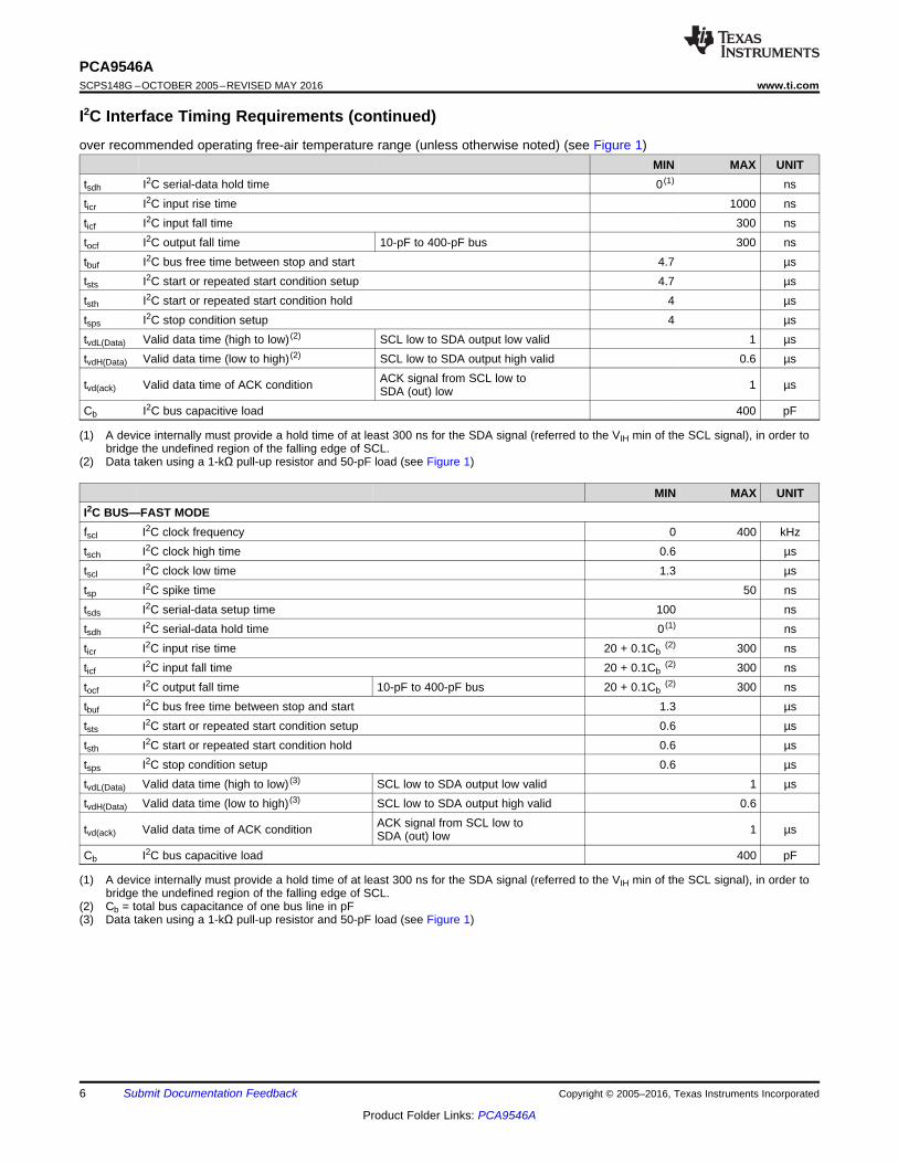
I2C Interface Timing Requirements (continued)over recommended operating free-air temperature range (unless otherwise noted) (see Figure 1)
MIN MAX UNIT
(1) A device internally must provide a hold time of at least 300 ns for the SDA signal (referred to the VIH min of the SCL signal), in order tobridge the undefined region of the falling edge of SCL.
(2) Data taken using a 1-kΩ pull-up resistor and 50-pF load (see Figure 1)
tsdh I2C serial-data hold time 0 (1) nsticr I2C input rise time 1000 nsticf I2C input fall time 300 nstocf I2C output fall time 10-pF to 400-pF bus 300 nstbuf I2C bus free time between stop and start 4.7 µststs I2C start or repeated start condition setup 4.7 µststh I2C start or repeated start condition hold 4 µstsps I2C stop condition setup 4 µstvdL(Data) Valid data time (high to low) (2) SCL low to SDA output low valid 1 µstvdH(Data) Valid data time (low to high) (2) SCL low to SDA output high valid 0.6 µs
tvd(ack) Valid data time of ACK condition ACK signal from SCL low toSDA (out) low 1 µs
Cb I2C bus capacitive load 400 pF
(1) A device internally must provide a hold time of at least 300 ns for the SDA signal (referred to the VIH min of the SCL signal), in order tobridge the undefined region of the falling edge of SCL.
(2) Cb = total bus capacitance of one bus line in pF(3) Data taken using a 1-kΩ pull-up resistor and 50-pF load (see Figure 1)
MIN MAX UNITI2C BUS—FAST MODEfscl I2C clock frequency 0 400 kHztsch I2C clock high time 0.6 µstscl I2C clock low time 1.3 µstsp I2C spike time 50 nstsds I2C serial-data setup time 100 nstsdh I2C serial-data hold time 0 (1) nsticr I2C input rise time 20 + 0.1Cb
(2) 300 nsticf I2C input fall time 20 + 0.1Cb
(2) 300 nstocf I2C output fall time 10-pF to 400-pF bus 20 + 0.1Cb
(2) 300 nstbuf I2C bus free time between stop and start 1.3 µststs I2C start or repeated start condition setup 0.6 µststh I2C start or repeated start condition hold 0.6 µstsps I2C stop condition setup 0.6 µstvdL(Data) Valid data time (high to low) (3) SCL low to SDA output low valid 1 µstvdH(Data) Valid data time (low to high) (3) SCL low to SDA output high valid 0.6
tvd(ack) Valid data time of ACK condition ACK signal from SCL low toSDA (out) low 1 µs
Cb I2C bus capacitive load 400 pF
7
PCA9546Awww.ti.com SCPS148G –OCTOBER 2005–REVISED MAY 2016
Product Folder Links: PCA9546A
Submit Documentation FeedbackCopyright © 2005–2016, Texas Instruments Incorporated
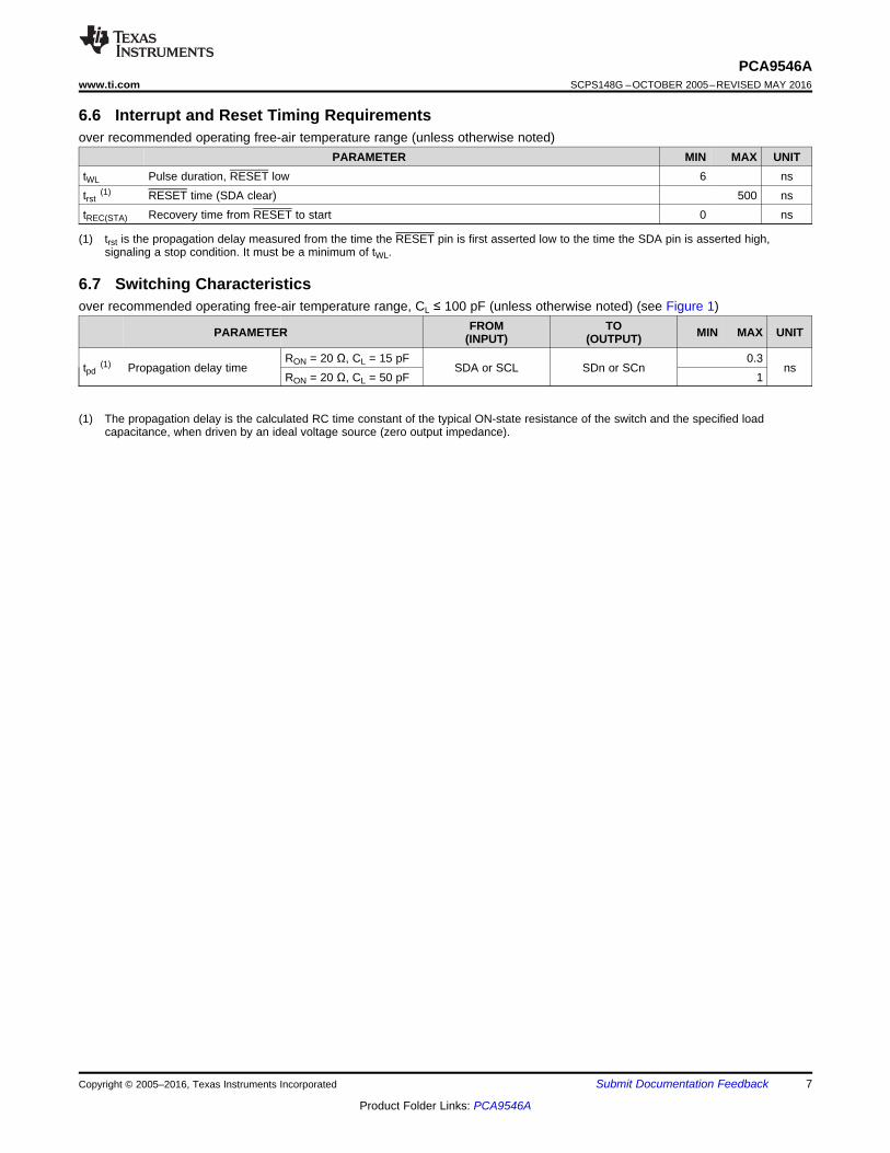
(1) trst is the propagation delay measured from the time the RESET pin is first asserted low to the time the SDA pin is asserted high,signaling a stop condition. It must be a minimum of tWL.
6.6 Interrupt and Reset Timing Requirementsover recommended operating free-air temperature range (unless otherwise noted)
PARAMETER MIN MAX UNITtWL Pulse duration, RESET low 6 nstrst
(1) RESET time (SDA clear) 500 nstREC(STA) Recovery time from RESET to start 0 ns
(1) The propagation delay is the calculated RC time constant of the typical ON-state resistance of the switch and the specified loadcapacitance, when driven by an ideal voltage source (zero output impedance).
6.7 Switching Characteristicsover recommended operating free-air temperature range, CL ≤ 100 pF (unless otherwise noted) (see Figure 1)
PARAMETER FROM(INPUT)
TO(OUTPUT) MIN MAX UNIT
tpd(1) Propagation delay time
RON = 20 Ω, CL = 15 pFSDA or SCL SDn or SCn
0.3ns
RON = 20 Ω, CL = 50 pF 1

RL = 1 kΩ
VCC
CL = 50 pF
(See Note 1)
tbuf
ticr
tsth tsds
tsdh
ticf
ticr
tscl tsch
tststvd(ACK)
or tvdL
tvdH
0.3 × VCC
Stop
Condition
tsps
Repeat
Start
ConditionStart or Repeat
Start Condition
SCL
SDA
Start
Condition
(S)
Address
Bit 7
(MSB)
Data
Bit 0
(LSB)
Stop
Condition
(P)
Two Bytes for Complete
Device Programming
I2C PORT LOAD CONFIGURATION
VOLTAGE WAVEFORMS
ticf
Stop
Condition
(P)
tsp
DUTSDn, SCn
0.7 × VCC
0.3 × VCC
0.7 × VCC
R/W
Bit 0
(LSB)
ACK
(A)
Data
Bit 7
(MSB)
Address
Bit 1
Address
Bit 6
ACK
(A)
BYTE DESCRIPTION
I2C address + R/W
Control register data
1
2
Copyright © 2016, Texas Instruments Incorporated
8
PCA9546ASCPS148G –OCTOBER 2005–REVISED MAY 2016 www.ti.com
Product Folder Links: PCA9546A
Submit Documentation Feedback Copyright © 2005–2016, Texas Instruments Incorporated
7 Parameter Measurement Information
(1) CL includes probe and jig capacitance.(2) All input pulses are supplied by generators having the following characteristics: PRR ≤ 10 MHz, ZO = 50 Ω,
tr/tf ≤ 30 ns.(3) The outputs are measured one at a time, with one transition per measurement.
Figure 1. I2C Interface Load Circuit, Byte Descriptions, and Voltage Waveforms

SCL
SDA
RESET
30%
50%
ACK or Read CycleStart
tREC
tWL
trst
9
PCA9546Awww.ti.com SCPS148G –OCTOBER 2005–REVISED MAY 2016
Product Folder Links: PCA9546A
Submit Documentation FeedbackCopyright © 2005–2016, Texas Instruments Incorporated
Parameter Measurement Information (continued)
Figure 2. Reset Timing

Copyright © 2016, Texas Instruments Incorporated
Input Filter I2C Bus Control
Power-On Reset
Switch Control Logic
PCA9546A
15
14
8
163
5
7
10
12
4
6
9
11
A0A1A2
12
13SDA
SCL
VCC
RESET
GND
SC0
SC1
SC2
SC3
SD0
SD1
SD2
SD3
10
PCA9546ASCPS148G –OCTOBER 2005–REVISED MAY 2016 www.ti.com
Product Folder Links: PCA9546A
Submit Documentation Feedback Copyright © 2005–2016, Texas Instruments Incorporated
8 Detailed Description
8.1 OverviewThe PCA9546A is a 4-channel, bidirectional translating I2C switch. The master SCL/SDA signal pair is directed tofour channels of slave devices, SC0/SD0-SC3/SD3. Any individual downstream channel can be selected as wellas any combination of the four channels.
The device offers an active-low RESET input which resets the state machine and allows the PCA9546A torecover should one of the downstream I2C buses get stuck in a low state. The state machine of the device canalso be reset by cycling the power supply, VCC, also known as a power-on reset (POR). Both the RESET functionand a POR will cause all channels to be deselected.
The connections of the I2C data path are controlled by the same I2C master device that is switched tocommunicate with multiple I2C slaves. After the successful acknowledgment of the slave address (hardwareselectable by A0 and A1 pins), a single 8-bit control register is written to or read from to determine the selectedchannels.
The PCA9546A may also be used for voltage translation, allowing the use of different bus voltages on eachSCn/SDn pair such that 1.8-V, 2.5-V, or 3.3-V parts can communicate with 5-V parts. This is achieved by usingexternal pull-up resistors to pull the bus up to the desired voltage for the master and each slave channel.
8.2 Functional Block Diagram

SDA
SCL
Data LineStable;
Data Valid
Changeof DataAllowed
11
PCA9546Awww.ti.com SCPS148G –OCTOBER 2005–REVISED MAY 2016
Product Folder Links: PCA9546A
Submit Documentation FeedbackCopyright © 2005–2016, Texas Instruments Incorporated
8.3 Feature DescriptionThe PCA9546A is a 4-channel, bidirectional translating switch for I2C buses that supports Standard-Mode (100kHz) and Fast-Mode (400 kHz) operation. The PCA9546A features I2C control using a single 8-bit control registerin which the four least significant bits control the enabling and disabling of the 4 switch channels of I2C data flow.Depending on the application, voltage translation of the I2C bus can also be achieved using the PCA9546A toallow 1.8-V, 2.5-V, or 3.3-V parts to communicate with 5-V parts. Additionally, in the event that communication onthe I2C bus enters a fault state, the PCA9546A can be reset to resume normal operation using the RESET pinfeature or by a power-on reset which results from cycling power to the device.
8.4 Device Functional Modes
8.4.1 RESET InputThe RESET input is an active-low signal that may be used to recover from a bus-fault condition. When this signalis asserted low for a minimum of tWL, the PCA9546A resets its registers and I2C state machine and deselects allchannels. The RESET input must be connected to VCC through a pull-up resistor.
8.4.1.1 RESET ErrataIf RESET voltage set higher than VCC, current will flow from RESET pin to VCC pin.
System ImpactVCC will be pulled above its regular voltage level
System WorkaroundDesign such that RESET voltage is same or lower than VCC
8.4.2 Power-On ResetWhen power is applied to VCC, an internal power-on reset holds the PCA9546A in a reset condition until VCC hasreached VPOR. At this point, the reset condition is released, and the PCA9546A registers and I2C state machineare initialized to their default states, all zeroes, causing all the channels to be deselected. Thereafter, VCC mustbe lowered below V POR to reset the device.
See the Power-On Reset Errata section.
8.5 Programming
8.5.1 I2C InterfaceThe I2C bus is for two-way two-line communication between different ICs or modules. The two lines are a serialdata line (SDA) and a serial clock line (SCL). Both lines must be connected to a positive supply via a pull-upresistor when connected to the output stages of a device. Data transfer can be initiated only when the bus is notbusy.
One data bit is transferred during each clock pulse. The data on the SDA line must remain stable during the highperiod of the clock pulse, as changes in the data line at this time are interpreted as control signals (see Figure 3).
Figure 3. Bit Transfer

SCL
MasterTransmitter/
ReceiverSlave
Receiver
SlaveTransmitter/
ReceiverMaster
Transmitter
MasterTransmitter/
Receiver
I2CMultiplexer
Slave
SDA
SDA
SCL
Start Condition
S
Stop Condition
P
12
PCA9546ASCPS148G –OCTOBER 2005–REVISED MAY 2016 www.ti.com
Product Folder Links: PCA9546A
Submit Documentation Feedback Copyright © 2005–2016, Texas Instruments Incorporated
Programming (continued)Both data and clock lines remain high when the bus is not busy. A high-to-low transition of the data line while theclock is high is defined as the start condition (S). A low-to-high transition of the data line while the clock is high isdefined as the stop condition (P) (see Figure 4).
Figure 4. Definition of Start and Stop Conditions
A device generating a message is a transmitter; a device receiving is the receiver. The device that controls themessage is the master, and the devices that are controlled by the master are the slaves (see Figure 5).
Figure 5. System Configuration
The number of data bytes transferred between the start and the stop conditions from transmitter to receiver is notlimited. Each byte of eight bits is followed by one acknowledge (ACK) bit. The transmitter must release the SDAline before the receiver can send an ACK bit.
When a slave receiver is addressed, it must generate an ACK after the reception of each byte. Also, a mastermust generate an ACK after the reception of each byte that has been clocked out of the slave transmitter. Thedevice that acknowledges must pull down the SDA line during the ACK clock pulse so that the SDA line is stablelow during the high pulse of the ACK-related clock period (see Figure 6). Setup and hold times must be takeninto account.

A NAS 1 1 1 0 A2 A1 A0 1SDA PB3 B2 B1 B0
Start Condition R/W ACK From Slave NACK From Master Stop Condition
Slave Address Control Register
0 0 0 0
A AS 1 1 1 0 A2 A1 A0 0
Start Condition
SDA
R/W ACK From Slave ACK From Slave
PB0B1B2B3XXXX
Stop Condition
Slave Address Control Register
Data Outputby Transmitter
SCL FromMaster
StartCondition
S
1 2 8 9
Data Outputby Receiver
Clock Pulse for ACK
NACK
ACK
13
PCA9546Awww.ti.com SCPS148G –OCTOBER 2005–REVISED MAY 2016
Product Folder Links: PCA9546A
Submit Documentation FeedbackCopyright © 2005–2016, Texas Instruments Incorporated
Programming (continued)
Figure 6. Acknowledgment on the I2C Bus
Data is transmitted to the PCA9546A control register using the write mode shown in Figure 7.
Figure 7. Write Control Register
Data is read from the PCA9546A control register using the read mode shown in Figure 8.
Figure 8. Read Control Register

Channel Selection Bits(Read/Write)
Channel 0
Channel 1
Channel 2
Channel 3
B3 B2 B1 B0
3 2 1 0
XXXX
4567
1 1 1 0 A1A2 A0
Slave Address
R/W
Fixed HardwareSelectable
14
PCA9546ASCPS148G –OCTOBER 2005–REVISED MAY 2016 www.ti.com
Product Folder Links: PCA9546A
Submit Documentation Feedback Copyright © 2005–2016, Texas Instruments Incorporated
8.6 Control Register
8.6.1 Device AddressFollowing a start condition, the bus master must output the address of the slave it is accessing. The address ofthe PCA9546A is shown in Figure 9. To conserve power, no internal pull-up resistors are incorporated on thehardware-selectable address pins, and they must be pulled high or low.
Figure 9. PCA9546A Address
The last bit of the slave address defines the operation to be performed. When set to a logic 1, a read is selected,while a logic 0 selects a write operation.
8.6.2 Control Register DescriptionFollowing the successful acknowledgment of the slave address, the bus master sends a byte to the PCA9546A,which is stored in the control register (see Figure 10). If multiple bytes are received by the PCA9546A, it will savethe last byte received. This register can be written and read via the I2C bus.
Figure 10. Control Register
8.6.3 Control Register DefinitionOne or several SCn/SDn downstream pairs, or channels, are selected by the contents of the control register (seeTable 1). This register is written after the PCA9546A has been addressed. The four LSBs of the control byte areused to determine which channel or channels are to be selected. When a channel is selected, the channelbecomes active after a stop condition has been placed on the I2C bus. This ensures that all SCn/SDn lines are ina high state when the channel is made active, so that no false conditions are generated at the time ofconnection. A stop condition always must occur right after the acknowledge cycle.

15
PCA9546Awww.ti.com SCPS148G –OCTOBER 2005–REVISED MAY 2016
Product Folder Links: PCA9546A
Submit Documentation FeedbackCopyright © 2005–2016, Texas Instruments Incorporated
Control Register (continued)
(1) Several channels can be enabled at the same time. For example, B3 =0, B2 = 1, B1 = 1, B0 = 0 means that channels 0 and 3 aredisabled, and channels 1 and 2 are enabled. Care must be taken not to exceed the maximum bus capacity.
Table 1. Control Register Write (Channel Selection), Control Register Read (Channel Status) (1)
B7 B6 B5 B4 B3 B2 B1 B0 COMMAND
X X X X X X X0 Channel 0 disabled1 Channel 0 enabled
X X X X X X0
XChannel 1 disabled
1 Channel 1 enabled
X X X X X0
X XChannel 2 disabled
1 Channel 2 enabled
X X X X0
X X XChannel 3 disabled
1 Channel 3 enabled
0 0 0 0 0 0 0 0 No channel selected,power-up/reset default state
9 Application and Implementation
9.1 Application InformationApplications of the PCA9546A will contain an I2C (or SMBus) master device and up to four I2C slave devices.The downstream channels are ideally used to resolve I2C slave address conflicts. For example, if four identicaldigital temperature sensors are needed in the application, one sensor can be connected at each channel: 0, 1, 2,and 3. When the temperature at a specific location must be read, the appropriate channel can be enabled and allother channels switched off, the data can be retrieved, and the I2C master can move on and read the nextchannel.
In an application where the I2C bus will contain many additional slave devices that do not result in I2C slaveaddress conflicts, these slave devices can be connected to any desired channel to distribute the total buscapacitance across multiple channels. If multiple switches will be enabled simultaneously, additional designrequirements must be considered (See Design Requirements and Detailed Design Procedure).
9.2 Typical ApplicationA typical application of the PCA9546A will contain anywhere from 1 to 5 separate data pull-up voltages, VDPUX ,one for the master device (VDPUM) and one for each of the selectable slave channels (VDPU0 – VDPU3). In theevent where the master device and all slave devices operate at the same voltage, then the pass voltage, Vpass =VDPUX. Once the maximum Vpass is known, VCC can be selected easily using Figure 12. In an application wherevoltage translation is necessary, additional design requirements must be considered (See Design Requirements).
Figure 11 shows an application in which the PCA9546A can be used.

PCA9546A
SD1
SDAChannel 0
Channel 1
Channel 2
Channel 3
I2C/SMBus
MasterSCL
RESET
SC1
SD2
SC2
SD3
SC3
SD0
SC0
VDPUM = 2.3 V to 5.5 VVCC= 3.3 V
VDPU0 = 2.3 V to 5.5 V
V = 2.3 V to 5.5 VDPU1
V = 2.3 V to 5.5 VDPU2
SDA
SCL
A2
A1
A0
GND
15
14
3
8
1
2
13
16
12
11
10
9
7
6
5
4VCC
V = 2.3 V to 5.5 VDPU3
Copyright © 2016, Texas Instruments Incorporated
16
PCA9546ASCPS148G –OCTOBER 2005–REVISED MAY 2016 www.ti.com
Product Folder Links: PCA9546A
Submit Documentation Feedback Copyright © 2005–2016, Texas Instruments Incorporated
Typical Application (continued)
Figure 11. PCA9546A Typical Application Schematic

rp(max)
b
tR
0.8473 C=
´
DPUX OL(max)
p(min)
OL
V VR
I
-
=
17
PCA9546Awww.ti.com SCPS148G –OCTOBER 2005–REVISED MAY 2016
Product Folder Links: PCA9546A
Submit Documentation FeedbackCopyright © 2005–2016, Texas Instruments Incorporated
Typical Application (continued)9.2.1 Design RequirementsThe A0, A1, and A2 pins are hardware selectable to control the slave address of the PCA9546A. These pins maybe tied directly to GND or VCC in the application.
If multiple slave channels will be activated simultaneously in the application, then the total IOL from SCL/SDA toGND on the master side will be the sum of the currents through all pull-up resistors, Rp.
The pass-gate transistors of the PCA9546A are constructed such that the VCC voltage can be used to limit themaximum voltage that is passed from one I2C bus to another.
Figure 12 shows the voltage characteristics of the pass-gate transistors (note that the graph was generated usingdata specified in the Electrical Characteristics section of this data sheet). In order for the PCA9546A to act as avoltage translator, the Vpass voltage must be equal to or lower than the lowest bus voltage. For example, if themain bus is running at 5 V and the downstream buses are 3.3 V and 2.7 V, Vpass must be equal to or below 2.7 Vto effectively clamp the downstream bus voltages. As shown in Figure 12, Vpass(max) is 2.7 V when the PCA9546Asupply voltage is 4 V or lower, so the PCA9546A supply voltage could be set to 3.3 V. Pull-up resistors then canbe used to bring the bus voltages to their appropriate levels (see Figure 11).
9.2.2 Detailed Design ProcedureOnce all the slaves are assigned to the appropriate slave channels and bus voltages are identified, the pull-upresistors, Rp, for each of the buses need to be selected appropriately. The minimum pull-up resistance is afunction of VDPUX, VOL,(max), and IOL as shown in Equation 1:
(1)
The maximum pull-up resistance is a function of the maximum rise time, tr (300 ns for fast-mode operation, fSCL =400 kHz) and bus capacitance, Cb as shown in Equation 2:
(2)
The maximum bus capacitance for an I2C bus must not exceed 400 pF for fast-mode operation. The buscapacitance can be approximated by adding the capacitance of the PCA9546A, Cio(OFF), the capacitance ofwires/connections/traces, and the capacitance of each individual slave on a given channel. If multiple channelswill be activated simultaneously, each of the slaves on all channels will contribute to total bus capacitance.

VDPUX (V)
Rp(
min
) (kO
hm)
0 0.5 1 1.5 2 2.5 3 3.5 4 4.5 5 5.50
0.2
0.4
0.6
0.8
1
1.2
1.4
1.6
1.8
D009
VDPUX > 2VVDPUX <= 2
Cb (pF)
Rp(
max
) (kO
hm)
0 50 100 150 200 250 300 350 400 4500
5
10
15
20
25
D008
Standard-modeFast-mode
2
Maximum
Typical
Minimum
VCC (V)
4.543.532.5 5 5.51
5
4.5
4
3.5
3
2.5
2
1.5
Vpa
ss (
V)
18
PCA9546ASCPS148G –OCTOBER 2005–REVISED MAY 2016 www.ti.com
Product Folder Links: PCA9546A
Submit Documentation Feedback Copyright © 2005–2016, Texas Instruments Incorporated
Typical Application (continued)9.2.3 PCA9546A Application Curves
Spacespacespace
Spacespacespace
Figure 12. Pass-Gate Voltage (Vpass) vs Supply Voltage(VCC) at Three Temperature Points
Standard-mode(fSCL= 100 kHz, tr = 1 µs)
Fast-mode(fSCL= 400 kHz, tr= 300 ns)
Figure 13. Maximum Pull-Up resistance (Rp(max)) vs BusCapacitance (Cb)
VOL = 0.2×VDPUX, IOL = 2 mA when VDPUX ≤ 2 VVOL = 0.4 V, IOL = 3 mA when VDPUX > 2 V
Figure 14. Minimum Pull-Up Resistance (Rp(min)) vs Pull-Up Reference Voltage (VDPUX)

19
PCA9546Awww.ti.com SCPS148G –OCTOBER 2005–REVISED MAY 2016
Product Folder Links: PCA9546A
Submit Documentation FeedbackCopyright © 2005–2016, Texas Instruments Incorporated
10 Power Supply RecommendationsThe operating power-supply voltage range of the PCA9546A is 2.3 V to 5.5 V applied at the VCC pin. When thePCA9546A is powered on for the first time or anytime the device must be reset by cycling the power supply, thepower-on reset requirements must be followed to ensure the I2C bus logic is initialized properly.
10.1 Power-On Reset ErrataA power-on reset condition can be missed if the VCC ramps are outside specification listed in Figure 15.
Figure 15. Power-On Reset Cycle
System ImpactIf ramp conditions are outside timing allowances above, POR condition can be missed, causing the device to lockup.
11 Layout
11.1 Layout GuidelinesFor PCB layout of the PCA9546A, common PCB layout practices must be followed but additional concernsrelated to high-speed data transfer such as matched impedances and differential pairs are not a concern for I2Csignal speeds. It is common to have a dedicated ground plane on an inner layer of the board and pins that areconnected to ground must have a low-impedance path to the ground plane in the form of wide polygon pours andmultiple vias. By-pass and de-coupling capacitors are commonly used to control the voltage on the VCC pin,using a larger capacitor to provide additional power in the event of a short power supply glitch and a smallercapacitor to filter out high-frequency ripple.
In an application where voltage translation is not required, all VDPUX voltages and VCC could be at the samepotential and a single copper plane could connect all of pull-up resistors to the appropriate reference voltage. Inan application where voltage translation is required, VDPUM, VDPU0, VDPU1, VDPU2, and VDPU3 may all be on thesame layer of the board with split planes to isolate different voltage potentials.
To reduce the total I2C bus capacitance added by PCB parasitics, data lines (SCn and SDn) must be a short aspossible and the widths of the traces must also be minimized (e.g. 5-10 mils depending on copper weight).

A0
A1
RESET
SD0
SC0
SD1
SC1
GND
VCC
SDA
SCL
A2
SC3
SD3
SC2
SD2
VDPU1
VDPU0
VIA to Power Plane
Partial Power Plane
VDPU3
VDPUM
VIA to GND Plane (Inner Layer)
Polygonal
Copper Pour
VCC
GND
By-pass/De-coupling
capacitors
PC
A9546A
GND
VDPU2
To I2C Master
To
Sla
ve
Ch
an
ne
l 3To
Sla
ve
Ch
an
ne
l 2To
Sla
ve
Ch
an
ne
l 1
To
Sla
ve
Ch
an
ne
l 0
LEGEND
20
PCA9546ASCPS148G –OCTOBER 2005–REVISED MAY 2016 www.ti.com
Product Folder Links: PCA9546A
Submit Documentation Feedback Copyright © 2005–2016, Texas Instruments Incorporated
11.2 Layout Example
12 Device and Documentation Support12.1 Electrostatic Discharge Caution
These devices have limited built-in ESD protection. The leads should be shorted together or the device placed in conductive foamduring storage or handling to prevent electrostatic damage to the MOS gates.
12.2 GlossarySLYZ022 — TI Glossary.
This glossary lists and explains terms, acronyms, and definitions.
13 Mechanical, Packaging, and Orderable InformationThe following pages include mechanical, packaging, and orderable information. This information is the mostcurrent data available for the designated devices. This data is subject to change without notice and revision ofthis document. For browser-based versions of this data sheet, refer to the left-hand navigation

PACKAGE OPTION ADDENDUM
www.ti.com 24-Aug-2018
Addendum-Page 1
PACKAGING INFORMATION
Orderable Device Status(1)
Package Type PackageDrawing
Pins PackageQty
Eco Plan(2)
Lead/Ball Finish(6)
MSL Peak Temp(3)
Op Temp (°C) Device Marking(4/5)
Samples
PCA9546AD ACTIVE SOIC D 16 40 Green (RoHS& no Sb/Br)
CU NIPDAU Level-1-260C-UNLIM -40 to 85 PCA9546A
PCA9546ADGVR ACTIVE TVSOP DGV 16 2000 Green (RoHS& no Sb/Br)
CU NIPDAU Level-1-260C-UNLIM -40 to 85 PD546A
PCA9546ADR ACTIVE SOIC D 16 2500 Green (RoHS& no Sb/Br)
CU NIPDAU Level-1-260C-UNLIM -40 to 85 PCA9546A
PCA9546ADT ACTIVE SOIC D 16 250 Green (RoHS& no Sb/Br)
CU NIPDAU Level-1-260C-UNLIM -40 to 85 PCA9546A
PCA9546ADW ACTIVE SOIC DW 16 40 Green (RoHS& no Sb/Br)
CU NIPDAU Level-1-260C-UNLIM -40 to 85 PCA9546A
PCA9546ADWG4 ACTIVE SOIC DW 16 40 Green (RoHS& no Sb/Br)
CU NIPDAU Level-1-260C-UNLIM -40 to 85 PCA9546A
PCA9546ADWR ACTIVE SOIC DW 16 2000 Green (RoHS& no Sb/Br)
CU NIPDAU Level-1-260C-UNLIM -40 to 85 PCA9546A
PCA9546APW ACTIVE TSSOP PW 16 90 Green (RoHS& no Sb/Br)
CU NIPDAU Level-1-260C-UNLIM -40 to 85 PD546A
PCA9546APWE4 ACTIVE TSSOP PW 16 90 Green (RoHS& no Sb/Br)
CU NIPDAU Level-1-260C-UNLIM -40 to 85 PD546A
PCA9546APWR ACTIVE TSSOP PW 16 2000 Green (RoHS& no Sb/Br)
CU NIPDAU Level-1-260C-UNLIM -40 to 85 PD546A
PCA9546APWRE4 ACTIVE TSSOP PW 16 2000 Green (RoHS& no Sb/Br)
CU NIPDAU Level-1-260C-UNLIM -40 to 85 PD546A
PCA9546APWRG4 ACTIVE TSSOP PW 16 2000 Green (RoHS& no Sb/Br)
CU NIPDAU Level-1-260C-UNLIM -40 to 85 PD546A
PCA9546APWT ACTIVE TSSOP PW 16 250 Green (RoHS& no Sb/Br)
CU NIPDAU Level-1-260C-UNLIM -40 to 85 PD546A
PCA9546APWTG4 ACTIVE TSSOP PW 16 250 Green (RoHS& no Sb/Br)
CU NIPDAU Level-1-260C-UNLIM -40 to 85 PD546A
PCA9546ARGVR ACTIVE VQFN RGV 16 2500 Green (RoHS& no Sb/Br)
CU NIPDAU Level-2-260C-1 YEAR -40 to 85 PD546A
PCA9546ARGYR ACTIVE VQFN RGY 16 3000 Green (RoHS& no Sb/Br)
CU NIPDAU Level-2-260C-1 YEAR -40 to 85 PD546A
(1) The marketing status values are defined as follows:ACTIVE: Product device recommended for new designs.

PACKAGE OPTION ADDENDUM
www.ti.com 24-Aug-2018
Addendum-Page 2
LIFEBUY: TI has announced that the device will be discontinued, and a lifetime-buy period is in effect.NRND: Not recommended for new designs. Device is in production to support existing customers, but TI does not recommend using this part in a new design.PREVIEW: Device has been announced but is not in production. Samples may or may not be available.OBSOLETE: TI has discontinued the production of the device.
(2) RoHS: TI defines "RoHS" to mean semiconductor products that are compliant with the current EU RoHS requirements for all 10 RoHS substances, including the requirement that RoHS substancedo not exceed 0.1% by weight in homogeneous materials. Where designed to be soldered at high temperatures, "RoHS" products are suitable for use in specified lead-free processes. TI mayreference these types of products as "Pb-Free".RoHS Exempt: TI defines "RoHS Exempt" to mean products that contain lead but are compliant with EU RoHS pursuant to a specific EU RoHS exemption.Green: TI defines "Green" to mean the content of Chlorine (Cl) and Bromine (Br) based flame retardants meet JS709B low halogen requirements of <=1000ppm threshold. Antimony trioxide basedflame retardants must also meet the <=1000ppm threshold requirement.
(3) MSL, Peak Temp. - The Moisture Sensitivity Level rating according to the JEDEC industry standard classifications, and peak solder temperature.
(4) There may be additional marking, which relates to the logo, the lot trace code information, or the environmental category on the device.
(5) Multiple Device Markings will be inside parentheses. Only one Device Marking contained in parentheses and separated by a "~" will appear on a device. If a line is indented then it is a continuationof the previous line and the two combined represent the entire Device Marking for that device.
(6) Lead/Ball Finish - Orderable Devices may have multiple material finish options. Finish options are separated by a vertical ruled line. Lead/Ball Finish values may wrap to two lines if the finishvalue exceeds the maximum column width.
Important Information and Disclaimer:The information provided on this page represents TI's knowledge and belief as of the date that it is provided. TI bases its knowledge and belief on informationprovided by third parties, and makes no representation or warranty as to the accuracy of such information. Efforts are underway to better integrate information from third parties. TI has taken andcontinues to take reasonable steps to provide representative and accurate information but may not have conducted destructive testing or chemical analysis on incoming materials and chemicals.TI and TI suppliers consider certain information to be proprietary, and thus CAS numbers and other limited information may not be available for release.
In no event shall TI's liability arising out of such information exceed the total purchase price of the TI part(s) at issue in this document sold by TI to Customer on an annual basis.

TAPE AND REEL INFORMATION
*All dimensions are nominal
Device PackageType
PackageDrawing
Pins SPQ ReelDiameter
(mm)
ReelWidth
W1 (mm)
A0(mm)
B0(mm)
K0(mm)
P1(mm)
W(mm)
Pin1Quadrant
PCA9546ADGVR TVSOP DGV 16 2000 330.0 12.4 6.8 4.0 1.6 8.0 12.0 Q1
PCA9546ADR SOIC D 16 2500 330.0 16.4 6.5 10.3 2.1 8.0 16.0 Q1
PCA9546ADWR SOIC DW 16 2000 330.0 16.4 10.75 10.7 2.7 12.0 16.0 Q1
PCA9546APWR TSSOP PW 16 2000 330.0 12.4 6.9 5.6 1.6 8.0 12.0 Q1
PCA9546APWT TSSOP PW 16 250 330.0 12.4 6.9 5.6 1.6 8.0 12.0 Q1
PCA9546ARGVR VQFN RGV 16 2500 330.0 12.4 4.25 4.25 1.15 8.0 12.0 Q2
PCA9546ARGYR VQFN RGY 16 3000 330.0 12.4 3.8 4.3 1.5 8.0 12.0 Q1
PACKAGE MATERIALS INFORMATION
www.ti.com 28-Apr-2016
Pack Materials-Page 1

*All dimensions are nominal
Device Package Type Package Drawing Pins SPQ Length (mm) Width (mm) Height (mm)
PCA9546ADGVR TVSOP DGV 16 2000 367.0 367.0 35.0
PCA9546ADR SOIC D 16 2500 333.2 345.9 28.6
PCA9546ADWR SOIC DW 16 2000 367.0 367.0 38.0
PCA9546APWR TSSOP PW 16 2000 367.0 367.0 35.0
PCA9546APWT TSSOP PW 16 250 367.0 367.0 35.0
PCA9546ARGVR VQFN RGV 16 2500 367.0 367.0 35.0
PCA9546ARGYR VQFN RGY 16 3000 367.0 367.0 35.0
PACKAGE MATERIALS INFORMATION
www.ti.com 28-Apr-2016
Pack Materials-Page 2


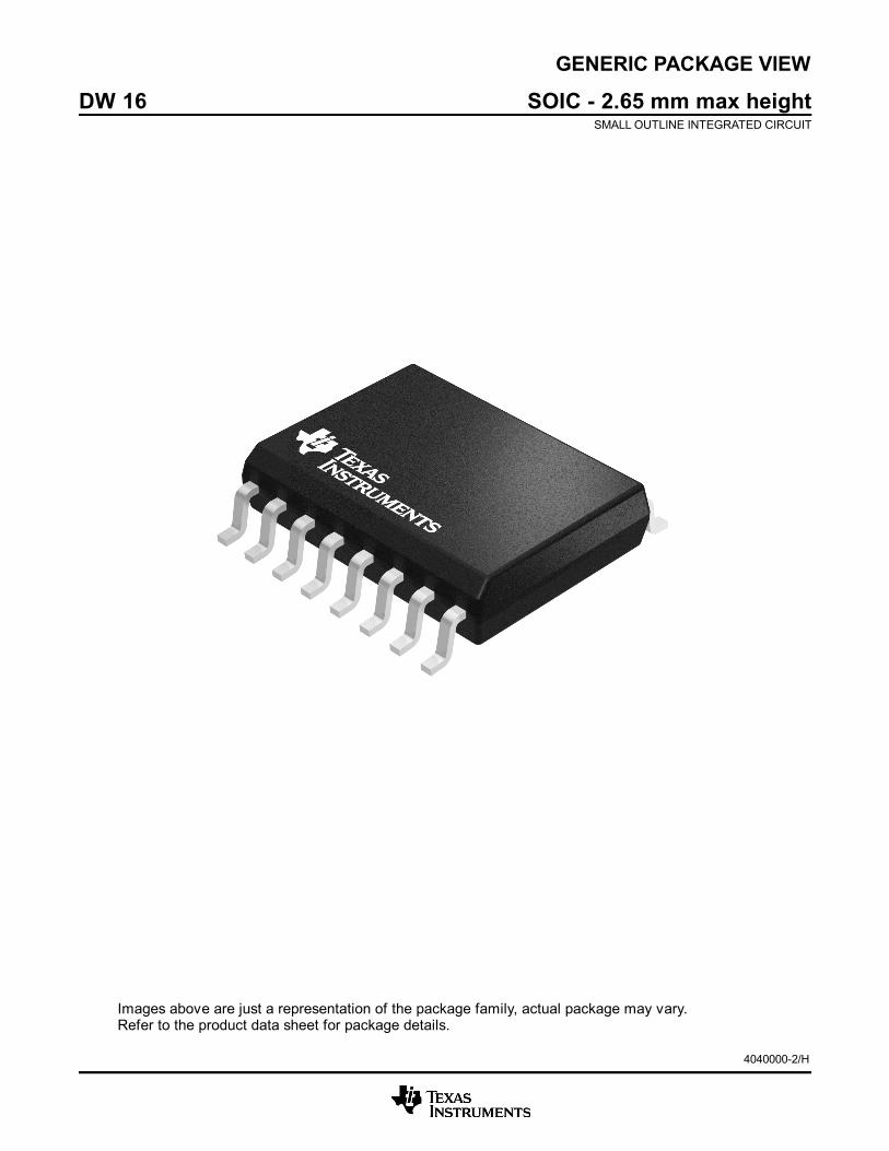
GENERIC PACKAGE VIEW
Images above are just a representation of the package family, actual package may vary.Refer to the product data sheet for package details.
DW 16 SOIC - 2.65 mm max heightSMALL OUTLINE INTEGRATED CIRCUIT
4040000-2/H

www.ti.com
PACKAGE OUTLINE
C
TYP10.639.97
2.65 MAX
14X 1.27
16X 0.510.31
2X8.89
TYP0.330.10
0 - 80.30.1
(1.4)
0.25GAGE PLANE
1.270.40
A
NOTE 3
10.510.1
BNOTE 4
7.67.4
4220721/A 07/2016
SOIC - 2.65 mm max heightDW0016ASOIC
NOTES: 1. All linear dimensions are in millimeters. Dimensions in parenthesis are for reference only. Dimensioning and tolerancing per ASME Y14.5M. 2. This drawing is subject to change without notice. 3. This dimension does not include mold flash, protrusions, or gate burrs. Mold flash, protrusions, or gate burrs shall not exceed 0.15 mm, per side. 4. This dimension does not include interlead flash. Interlead flash shall not exceed 0.25 mm, per side.5. Reference JEDEC registration MS-013.
1 16
0.25 C A B
98
PIN 1 IDAREA
SEATING PLANE
0.1 C
SEE DETAIL A
DETAIL ATYPICAL
SCALE 1.500

www.ti.com
EXAMPLE BOARD LAYOUT
0.07 MAXALL AROUND
0.07 MINALL AROUND
(9.3)
14X (1.27)
R0.05 TYP
16X (2)
16X (0.6)
4220721/A 07/2016
SOIC - 2.65 mm max heightDW0016ASOIC
NOTES: (continued) 6. Publication IPC-7351 may have alternate designs. 7. Solder mask tolerances between and around signal pads can vary based on board fabrication site.
METAL SOLDER MASKOPENING
NON SOLDER MASKDEFINED
SOLDER MASK DETAILS
OPENINGSOLDER MASK METAL
SOLDER MASKDEFINED
LAND PATTERN EXAMPLESCALE:7X
SYMM
1
8 9
16
SEEDETAILS
SYMM

www.ti.com
EXAMPLE STENCIL DESIGN
R0.05 TYP
16X (2)
16X (0.6)
14X (1.27)
(9.3)
4220721/A 07/2016
SOIC - 2.65 mm max heightDW0016ASOIC
NOTES: (continued) 8. Laser cutting apertures with trapezoidal walls and rounded corners may offer better paste release. IPC-7525 may have alternate design recommendations. 9. Board assembly site may have different recommendations for stencil design.
SOLDER PASTE EXAMPLEBASED ON 0.125 mm THICK STENCIL
SCALE:7X
SYMM
SYMM
1
8 9
16

IMPORTANT NOTICE
Texas Instruments Incorporated (TI) reserves the right to make corrections, enhancements, improvements and other changes to itssemiconductor products and services per JESD46, latest issue, and to discontinue any product or service per JESD48, latest issue. Buyersshould obtain the latest relevant information before placing orders and should verify that such information is current and complete.TI’s published terms of sale for semiconductor products (http://www.ti.com/sc/docs/stdterms.htm) apply to the sale of packaged integratedcircuit products that TI has qualified and released to market. Additional terms may apply to the use or sale of other types of TI products andservices.Reproduction of significant portions of TI information in TI data sheets is permissible only if reproduction is without alteration and isaccompanied by all associated warranties, conditions, limitations, and notices. TI is not responsible or liable for such reproduceddocumentation. Information of third parties may be subject to additional restrictions. Resale of TI products or services with statementsdifferent from or beyond the parameters stated by TI for that product or service voids all express and any implied warranties for theassociated TI product or service and is an unfair and deceptive business practice. TI is not responsible or liable for any such statements.Buyers and others who are developing systems that incorporate TI products (collectively, “Designers”) understand and agree that Designersremain responsible for using their independent analysis, evaluation and judgment in designing their applications and that Designers havefull and exclusive responsibility to assure the safety of Designers' applications and compliance of their applications (and of all TI productsused in or for Designers’ applications) with all applicable regulations, laws and other applicable requirements. Designer represents that, withrespect to their applications, Designer has all the necessary expertise to create and implement safeguards that (1) anticipate dangerousconsequences of failures, (2) monitor failures and their consequences, and (3) lessen the likelihood of failures that might cause harm andtake appropriate actions. Designer agrees that prior to using or distributing any applications that include TI products, Designer willthoroughly test such applications and the functionality of such TI products as used in such applications.TI’s provision of technical, application or other design advice, quality characterization, reliability data or other services or information,including, but not limited to, reference designs and materials relating to evaluation modules, (collectively, “TI Resources”) are intended toassist designers who are developing applications that incorporate TI products; by downloading, accessing or using TI Resources in anyway, Designer (individually or, if Designer is acting on behalf of a company, Designer’s company) agrees to use any particular TI Resourcesolely for this purpose and subject to the terms of this Notice.TI’s provision of TI Resources does not expand or otherwise alter TI’s applicable published warranties or warranty disclaimers for TIproducts, and no additional obligations or liabilities arise from TI providing such TI Resources. TI reserves the right to make corrections,enhancements, improvements and other changes to its TI Resources. TI has not conducted any testing other than that specificallydescribed in the published documentation for a particular TI Resource.Designer is authorized to use, copy and modify any individual TI Resource only in connection with the development of applications thatinclude the TI product(s) identified in such TI Resource. NO OTHER LICENSE, EXPRESS OR IMPLIED, BY ESTOPPEL OR OTHERWISETO ANY OTHER TI INTELLECTUAL PROPERTY RIGHT, AND NO LICENSE TO ANY TECHNOLOGY OR INTELLECTUAL PROPERTYRIGHT OF TI OR ANY THIRD PARTY IS GRANTED HEREIN, including but not limited to any patent right, copyright, mask work right, orother intellectual property right relating to any combination, machine, or process in which TI products or services are used. Informationregarding or referencing third-party products or services does not constitute a license to use such products or services, or a warranty orendorsement thereof. Use of TI Resources may require a license from a third party under the patents or other intellectual property of thethird party, or a license from TI under the patents or other intellectual property of TI.TI RESOURCES ARE PROVIDED “AS IS” AND WITH ALL FAULTS. TI DISCLAIMS ALL OTHER WARRANTIES ORREPRESENTATIONS, EXPRESS OR IMPLIED, REGARDING RESOURCES OR USE THEREOF, INCLUDING BUT NOT LIMITED TOACCURACY OR COMPLETENESS, TITLE, ANY EPIDEMIC FAILURE WARRANTY AND ANY IMPLIED WARRANTIES OFMERCHANTABILITY, FITNESS FOR A PARTICULAR PURPOSE, AND NON-INFRINGEMENT OF ANY THIRD PARTY INTELLECTUALPROPERTY RIGHTS. TI SHALL NOT BE LIABLE FOR AND SHALL NOT DEFEND OR INDEMNIFY DESIGNER AGAINST ANY CLAIM,INCLUDING BUT NOT LIMITED TO ANY INFRINGEMENT CLAIM THAT RELATES TO OR IS BASED ON ANY COMBINATION OFPRODUCTS EVEN IF DESCRIBED IN TI RESOURCES OR OTHERWISE. IN NO EVENT SHALL TI BE LIABLE FOR ANY ACTUAL,DIRECT, SPECIAL, COLLATERAL, INDIRECT, PUNITIVE, INCIDENTAL, CONSEQUENTIAL OR EXEMPLARY DAMAGES INCONNECTION WITH OR ARISING OUT OF TI RESOURCES OR USE THEREOF, AND REGARDLESS OF WHETHER TI HAS BEENADVISED OF THE POSSIBILITY OF SUCH DAMAGES.Unless TI has explicitly designated an individual product as meeting the requirements of a particular industry standard (e.g., ISO/TS 16949and ISO 26262), TI is not responsible for any failure to meet such industry standard requirements.Where TI specifically promotes products as facilitating functional safety or as compliant with industry functional safety standards, suchproducts are intended to help enable customers to design and create their own applications that meet applicable functional safety standardsand requirements. Using products in an application does not by itself establish any safety features in the application. Designers mustensure compliance with safety-related requirements and standards applicable to their applications. Designer may not use any TI products inlife-critical medical equipment unless authorized officers of the parties have executed a special contract specifically governing such use.Life-critical medical equipment is medical equipment where failure of such equipment would cause serious bodily injury or death (e.g., lifesupport, pacemakers, defibrillators, heart pumps, neurostimulators, and implantables). Such equipment includes, without limitation, allmedical devices identified by the U.S. Food and Drug Administration as Class III devices and equivalent classifications outside the U.S.TI may expressly designate certain products as completing a particular qualification (e.g., Q100, Military Grade, or Enhanced Product).Designers agree that it has the necessary expertise to select the product with the appropriate qualification designation for their applicationsand that proper product selection is at Designers’ own risk. Designers are solely responsible for compliance with all legal and regulatoryrequirements in connection with such selection.Designer will fully indemnify TI and its representatives against any damages, costs, losses, and/or liabilities arising out of Designer’s non-compliance with the terms and provisions of this Notice.
Mailing Address: Texas Instruments, Post Office Box 655303, Dallas, Texas 75265Copyright © 2018, Texas Instruments Incorporated