Embed Size (px)
Citation preview

Partial Discharge Analysis in HVDC Gas Insulated Substations
Roland Piccin
Supervisor: Dr.ir. Peter H.F. Morshuis Daily Supervisor: Dr.ir. Armando Rodrigo Mor
JULY 2013 DEPARTMENT OF INTELLIGENT ELECTRICAL POWER GRIDS

1
To Carlo, Denise and Silvia

2
Summary
Nowadays, Gas Insulated Substations (GIS) are vital nodes of the Transmission Network due to their compact dimensions permitted by the use of SF6 as insulating medium and the high reliability guaranteed. Nonetheless, the strictly requirements of safety in operation and continuous power supply catalyse the attention to improve the reliability and the maintenance strategies of these installations. Though, Partial Discharge (PD) monitoring is accredited as a fundamental tool for Alternate Current (AC) GIS diagnostic, it has been little investigated for Direct Current (DC) applications. In fact, the growing demand of High Voltage Direct Current (HVDC) transmission brings up the issue of maintainability of HVDC apparatus.
In this frame, this Thesis Project aims to investigate the detection and the recognition of PD under DC conditions.
In Chapter 1 is presented the current state-of-the-art of HVDC converter technologies and the converter used during the laboratory part of the project. In addition, the description of a GIS installation is given along with its main causes of failure. To conclude the Introduction, the Project Description is reported with scope, objectives and project stages.
As PD is a complex and chaotic phenomenon, it must be interpreted at the light of its physical mechanism. Chapter 2 aims to provide a review of the theory behind PD occurrence, starting from the electron which ignites the avalanche to the modelling of the discharge. The focus is given predominantly to PD occurring in gases and the comparison between AC and DC. In the Chapter are defined many recurrent terms in the Thesis work.
The major part of the project is carried on in the High Voltage Laboratory of TU Delft. Consequently, Chapter 3 is devoted to the description of everything that is related with the measurements. The HVDC and HVAC test set-up are introduced. Among the project’s objectives there is the comparison of the conventional IEC 60270 detection system and the Ultra High Frequency (UHF) method by means of internal antenna, thus a relevant part of the Chapter is dedicated to the detection systems and their components. The understanding of the detection not only permits to set the limitations and the potentialities of the system but it also helps the analysis of the measurement results.
Chapter 4 deals with the recognition of the PD under DC. At first, it is given an overview of an intelligent system for the automatic PD recognition and the eligible recognition techniques. In the second instance, it is described the spectrum analysis applied for PD recognition under DC. The detection units used for the recognition are the Spectrum Analyser (SA) and the digital PD detector

3
PDBaseII. The latter is used for the time-domain analysis. In addition, the limitations and the strength of the techniques are highlighted.
The Experimental Results and the Discussion is treated in Chapter 5. The results are divided for the three defects investigated namely High Voltage (HV) protrusion, Low Voltage (LV) protrusion and Free Moving Particle. At first, for each defect the results are separated for AC, Negative DC and Positive DC; afterwards the results are compared and explained in the Discussion.
Finally, the main Conclusion and Recommendations are given in Chapter 6. The Conclusions regard the PD mechanism under AC and DC, the comparison between IEC 60270 and UHF detection systems and the recognition of PD under DC. Furthermore, a few remarks and advises on the future continuation of the research are given at the end.

4
Contents
Summary ................................................................................................................................................. 2
Chapter 1 - Introduction .......................................................................................................................... 8
1.1 High Voltage Direct Current – Prospective ........................................................................ 8
1.2 Generation of HVDC .......................................................................................................... 9
1.2.1 Voltage Source Converter (VSC) ................................................................................ 9
1.2.2 HVDC in the TU Delft Laboratory ............................................................................. 10
1.3 Gas Insulated Substations ............................................................................................... 11
1.4 Thesis project description ............................................................................................... 12
Chapter 2 - Partial discharge phenomena ............................................................................................. 14
2.1 Partial discharge physics.................................................................................................. 14
2.1.1 Ionization .................................................................................................................. 14
2.1.2 Electron emission from the electrodes .................................................................... 16
2.1.3 Avalanches ................................................................................................................ 17
2.1.4 Deionization .............................................................................................................. 18
2.2 Discharge mechanism ...................................................................................................... 20
2.2.1 Townsend mechanism .............................................................................................. 20
2.2.2 Streamer mechanism ............................................................................................... 22
2.2.3 Leader mechanism ................................................................................................... 23
2.3 Internal discharges .......................................................................................................... 24
2.3.1 Equivalent circuit at AC voltage ................................................................................ 24
2.3.2 Equivalent circuit at DC voltage................................................................................ 27
2.4 Surface discharge ............................................................................................................ 31
2.4.1 Charge accumulation mechanisms ........................................................................... 31

5
2.4.2 Particle contamination at the spacer ...................................................................... 32
2.5 Corona discharge ............................................................................................................. 34
2.5.1 Negative corona ....................................................................................................... 34
2.5.2 Positive corona ......................................................................................................... 34
2.5.3 Comparison of DC negative and positive corona ..................................................... 35
Chapter 3 - Measurement set-up and detection systems ..................................................................... 36
3.1 High Voltage circuit ......................................................................................................... 36
3.2 Test object ....................................................................................................................... 38
3.3 Detection units ................................................................................................................ 39
3.4 IEC 60270 – Conventional detection method ................................................................. 43
3.4.1 Coupling modes ....................................................................................................... 43
3.4.2 Coupling capacitor Ck ............................................................................................... 44
3.4.3 Coupling device CD .................................................................................................. 45
3.4.4 Calibration ............................................................................................................... 47
3.5 Ultra High Frequency (UHF) – Non-conventional method .............................................. 48
3.5.1 Electromagnetic wave propagation in GIS ............................................................... 48
3.5.2 UHF detection system .............................................................................................. 51
3.5.3 Sensitivity check ....................................................................................................... 53
3.6 Noise and denoising ........................................................................................................ 54
3.6.1 The noise issue ......................................................................................................... 54
3.6.2 Denoising .................................................................................................................. 56
Chapter 4 - Partial discharge recognition ............................................................................................. 60
4.1 Online Condition Monitoring........................................................................................... 60
4.2 Measured data ................................................................................................................ 61
4.3 Feature extraction ........................................................................................................... 63
4.3.1 Statistical moments .................................................................................................. 63

6
4.3.2 Wavelet Analysis ....................................................................................................... 64
4.3.3 Independent Component Analysis ........................................................................... 65
4.4 Classification .................................................................................................................... 66
4.4.1 Artificial Neural Networks ........................................................................................ 66
4.4.2 Clustering method .................................................................................................... 67
4.5 Spectrum Analysis ........................................................................................................... 68
4.5.1 Frequency domain analysis ...................................................................................... 70
4.5.2 Time domain analysis ............................................................................................... 74
Chapter 5 - Experimental results and discussion .................................................................................. 79
5.1 High Voltage Protrusion .................................................................................................. 79
5.1.1 AC Voltage ................................................................................................................ 79
5.1.2 Negative DC Voltage ................................................................................................. 83
5.1.3 Positive DC Voltage ................................................................................................... 86
5.1.4 Discussion ................................................................................................................. 89
5.2 Low Voltage Protrusion ................................................................................................... 91
5.2.1 AC Voltage ................................................................................................................ 92
5.2.2 Negative DC Voltage ................................................................................................. 96
5.2.3 Positive DC Voltage ................................................................................................. 100
5.2.4 Discussion ............................................................................................................... 102
5.3 Free Moving Particle ...................................................................................................... 103
5.3.1 Particle Motion ....................................................................................................... 104
5.3.2 AC Voltage .............................................................................................................. 106
5.3.3 DC Voltage .............................................................................................................. 109
5.3.4 Discussion ............................................................................................................... 113
Chapter 6 - Conclusions and recommendations for future research .................................................. 117
6.1 Conclusions .................................................................................................................... 117

7
6.2 Recommendations for future research ......................................................................... 119
Appendix A - Repetition rate check ..................................................................................................... 120
A.1 Introduction................................................................................................................. .122
A.2 Test Procedure ............................................................................................................. 121
A.3 PD BaseII ........................................................................................................................ 123
A.3.1 IEC 60270 Mode ..................................................................................................... 124
A.3.2 Wide Band (WB) Mode .......................................................................................... 126
A.4 Spectrum Analyser (SA) ................................................................................................. 128
Appendix B - Acquisition modes of PDBaseII ..................................................................................... 132
Appendix C - Spectrum Analyzer Fundamentals ................................................................................. 130
Appendix D - Sensitivity check............................................................................................................. 137
Acknowledgments ............................................................................................................................... 139
Bibliography ...................................................................................................................................... 140

8
Chapter 1
This Chapter introduces the scope of the thesis putting into context the project goals in view of the trends in the transmission network to the High Voltage Direct Current (HVDC) technologies. It will be given an overview of the current technologies for HVDC converter substations. Additionally, the Gas Insulated Systems (GIS) are described. Since GIS are fundamental nodes of a modern Transmission Network, their maintenance and monitoring gain more and more importance. Among others monitoring techniques, Partial Discharge (PD) detection and analysis is a widely recognized tool for prevention of failures. In this framework, the project objectives are presented at the end of the Chapter.
1.1 High Voltage Direct Current – Prospective
At the end of the 19th century, the dawn of the Electrical Power Industry, a passionate debate developed over the generation of electricity and its distribution. The outcome determined the structure of the power grid as we know it nowadays. The most representative players of the dispute, so fierce that is also known as the “Battle of the currents”, were Nikola Tesla and Thomas Edison, the former a supporter of the electric distribution in Alternate Current (AC) and the latter a supporter of the Direct Current (DC). In spite of the well-known result of the “battle”, nowadays we are seeing a revival of DC, not only at the transmission level. In fact, the DC solutions include, among others, renewable energy integration (e.g. solar energy systems), charging of electric vehicles, data center supply and, of course, long HVDC interconnections.
The first modern HVDC interconnections were the Moscow-Kashira system and the connection Gotland-Sweden mainland in 1954. Since then, big steps has been done in the development of HVDC converters whose employment is driven by several technical and economic factors, to mention a few [1]:
• Lower overall investment; • Lower losses, due to only active power flow; • Increased stability and improvements in power quality;
INTRODUCTION

9
• Less expensive circuit breakers in the AC side and simpler bus-bar arrangements in switch-yard due to lower short-circuit currents;
According to a recent report from Pike Research, one of the fastest-growing markets in the utility sector is HVDC transmission [1]. The report claims investment growth by 44% over the next five years, from the 8.4 billion US$ in 2010 to 12.1 billion US$ in 2015. The growth is driven by the need for very long interconnections mainly in China and India but also in Brazil. The US and European market will see also a significant development.
1.2 Generation of HVDC
1.2.1 Voltage Source Converter (VSC)
Traditionally, HVDC converters are based on line-commuted thyristors valves. Even though, this technology is well-tested it presents also pitfalls such as generation of harmonics and absorption of reactive power. Nowadays, the frontline in HVDC technologies is represented by Voltage Source Converters (VSCs) which are based on self-commutating devices such as Insulated Gate Bipolar Transistors (IGBTs). IGBTs have the capability to be turned-on and –off by command, a peculiarity that renders these devices particularly attractive for the elimination of harmonics and voltage control. Though VSC are developed in different topologies, the Modular Multilevel Converter (M2C) is accredited to be the most promising for HVDC transmission. In Figure 1.1 the M2C topology is schematically represented. The fundamental component of the converter is the module composed by IGBTs and a capacitor which makes each module itself a voltage source. Therefore the module can create three voltage outputs: two little voltage step of different polarity and zero voltage. The modules are then cascade-connected constituting the converter arm. The number of modules connected varies with the desired level of voltage generated. Generally, there are from 100 to 200 modules per arm.
Figure 1.1 – Basic scheme of a M2C converter. Cascade connected modules constitute the converter’s arms.

10
This topology is differently developed by the three major HVDC converter manufacturers: Alstom with HVDC MaxSine, ABB with HVDC Light, Siemens with HVDC Plus.
Siemens was the first company to build a M2C link in the San Francisco area, the Trans Bay link completed in 2010. HVDC Light has the topology of the converter shown in Figure 1.1 and it is composed by half-bridge modules. Alstom MaxSine keeps the same topology of HVDC Light but it has full-bridge modules. Though this solution is more costly, it brings several advantages, among others the possibility to invert the voltage polarity on the DC side. Instead, for HVDC Light ABB developed a different solution called Cascade Two-Levels (CTL). Though the topology is still a multi-level with half bridge modules, the sub-modules are constituted by strings of IGBTs in series that achieves a higher reliability.
1.2.2 HVDC in the TU Delft Laboratory
The measurements in the TU Delft High Voltage Laboratory have been performed under HVDC supplied by Heinzinger PNC 100000 high-precision power supply.
Figure 1.2 – Internal circuit scheme of the Heinzinger PNC 100000 [2].
Figure 1.2 shows the internal circuit of the power supply. At first the AC grid voltage is rectified. Afterwards the voltage is converted to a rectangular 30 kHz AC voltage which feeds the transformer in order to generate HV. The secondary voltage is then multiplied and rectified by a multi-stage cascade converter. The output is then properly filtered to reduce the ripple. Voltage and current are measured at the output in order to feed-back the Pulse Width Modulation (PWM) control. The device can produce both DC polarities by inverting the rectifier box. The nominal voltage output is 100 kV.

11
1.3 Gas Insulated Substations
Gas Insulated Substations (GISs) respond to the expansion of the grid as well as the scarcity of available locations to build substations. In fact, GIS are multi-equipment systems in which the insulating medium is mainly Hexafluoride (SF6) whose insulating properties permits to drastically reduce the dimensions of the substation in comparison to a traditional open-air one. The GIS have a sealed metal-enclosure that keeps the gas under pressure and avoids leakage of SF6, a strong green-house gas. In Figure 1.3 is shown a representation of a section of a GIS. The systems is composed both of primary equipment (e.g circuit breaker) and secondary equipment (e.g. current transformer) and it can be installed in open-air or inside a building as it is permitted by the compact dimensions.
Figure 1.3 – Representation of a Gas Insulated System: 1- Earthing Switch; 2 – Busbar disconnector; 3 – Circuit breaker; 4 – Spring operating mechanism; 5 – Current transformer; 6 – Feeder disconnector; 7 – Cable termination enclosure; 8 – Voltage transformer. The images refers to a B105 Alstom GIS.
Although GIS have low-maintenance requirement, the equipment reliability may be hindered by undesired metal particle which subjected to an intense electric field can create Partial Discharges (PDs). PDs are responsible for many failure mechanisms of GIS. To mention only few of them, a free moving particle approaching the conductor may trigger a flashover or if it lays on a spacer can lead to the carbonization of the latter. PDs are also responsible for generation of corrosive by-products of SF6 which are harmful for both spacers and conductive parts. The principal PD sources responsible for failures of GIS are:
• Fixed protrusion; • Free moving particle; • Floating electrode; • Particle fixed on the spacer surface; • Void in insulators.

12
A service experience study reported by C. Nuemann in [3] on 123 kV and 420 kV GIS, shows the main causes of dielectric failure. From Figure 1.4 appears that at least 50% of the causes of failures, both for 123 kV and 420 kV GIS, are related to defects that are detectable by PD diagnostic and in particular related to particle on surface, on enclosure and on HV conductor. Furthermore, from 60% to 70% of the failures could have been detected by monitoring systems with a sufficient sensitivity [3]. These figures mark the relevant role played by PD monitoring as a potential tool for failure prevention and maintenance scheduling.
Figure 1.4 – Pie chart of the main causes of failures in 123 kV GIS and 420 kV GIS according with a study of some German utilities [3].
1.4 Thesis Project Description
PD monitoring is widely used for HV equipment diagnostic. However, the standardized procedure IEC 60270 is only applicable offline which implies turn-off costs and limited capabilities in effective maintenance strategies; therefore, on-line condition monitoring systems gain more and more relevance among manufactures and utilities. The Ultra High Frequency (UHF) method is becoming widely used for online PD monitoring in GIS. In view of the rapid growth of HVDC transmission, the purpose of the project is to investigate the possibility to extend the UHF technique to measure PD caused under DC voltage.

13
In the light of the project purpose the following objectives are established:
1. Investigate and interpret the physical behaviour of PDs caused by protrusions and free moving particle in a GIS under AC and DC. Differences and common PD characteristic features will be determined.
2. Comparison of IEC 60270 and UHF methods in terms of sensitivity and information provided. 3. Determination of the limitations and potentialities of the UHF method for the detection and
recognition of PD under DC.
The project is then divided in three stages:
1. Literature review. An extensive study of PD mechanism under AC and DC, of the detection systems and of the recognition of discharge. The focus is kept to DC and GIS.
2. Experimental research (TU Delft High Voltage Laboratory). A dedicated measurement set-up is built for investigation of PD caused by protrusion on the conductor, on the GIS enclosure and by a free moving particle. At first AC voltage is applied then DC of both polarities. Several variants of the conventional and UHF detection system are employed.
3. Analysis of the measurements. The results obtained and the analysis method employed differ from one detection unit to another. On one hand, the results are used to understand the PD physics and, on the other hand, the focus is given to extract features for the PD recognition.
The project has been arranged with Alstom Grid in the frame of a lasting collaboration with the High Voltage Technology and Management Department of TU Delft. According with the plan, several meetings are scheduled with Alstom in order to present the results and specify the guidelines.

14
Chapter 2
A gaseous dielectric is composed of atoms and molecules in continuous and chaotic movement due to thermal agitation; free electrons are generated by collisions between gas molecules or by external radiation sources such as the cosmic radiation. The mechanism that separates an electron from an atom or molecule is called ionization and it is fundamental for the initiation of the discharge. However, an electron emission may also occur at the metal surface of the electrical equipment. Whenever a free electron is subjected to an electric field, it is accelerated in the direction of the field; successive collisions may lead to ionization of gas molecules. Under certain conditions, discussed below, a discharge is created by an electron avalanche. The processes that lead to a discharge in a gaseous dielectric depends upon several conditions (e.g. pressure). Three mechanisms will be discussed in this chapter: Townsend-like, Streamer-like, Leader-like. Further, description is given of internal discharge, surface discharge and corona discharges.
2.1 Partial Discharge Physics
2.1.1 Ionization
Referring to the atom’s model of Bohr-Rutherford, the electrons follow orbits of different radius around the nucleus. Since the external orbits are characterized by an higher energy content, an atom acquires more energy if an electron moves from an internal to an external orbit. Ultimately, an atom achieves its maximum energy when it loses an electron. This process is called ionization. Between the normal status and the ionization, the atom may be in several unstable excited status. The energy required by the electron to move from an orbit to a higher energy orbit is measured in electronvolt [eV] and it varies from gas to gas.
PARTIAL DISCHARGE PHENOMENA

15
Ionization by collision
The chaotic movement of the gas molecules results in continuous collisions with consequent energy variation of the molecules themselves. Depending on the energy exchange mechanism involved in the collision, it is possible to identify two types of collision:
• Elastic collision involves only a kinetic energy transfer between two molecules. No variation of internal energy occurs, consequently the atomic structure of the molecules remains unvaried.
• Inelastic collision between two molecules entails the absorption of energy needed to modify the atomic structure of the molecule. This collision leads to the excitation or ionization of the gas atom.
The excitation of the gas atom caused by the impact of an electron requires, at least, the energy to move an electron to the adjacent orbit. This process may be described by the following formula
A + e → A* + e
where A stands for the atom, e for electron and A* for the excited state of the atom. However, the new excited state is unstable. In less than a µs the atom restores its basic state radiating a photon
A* → A + hν
Where h is the Planck’s constant and ν the frequency of radiation [4].
In case that the moving electron has a kinetic energy high enough to be at least equal to the ionization potential of the colliding atoms, the collision liberates another electron, namely the atom is ionized. The energy necessary to the process depends on the gas; it varies from a few eV to approximately 25 eV [4]. The process is described as follows
A + e → A+ +2e
A+ is the ionized atom.
Photo ionization
Travelling photons may have the energy content sufficient to liberate an electron following the impact with a gas atom, such that
A + hν → A+ +e
The condition necessary to liberate an electron is described by the following relation
hν ≥ eVi
eVi is the ionization potential of the gas atom. If the above relation holds, the emission of a photo-electron occurs. The energy of the photo-electron may be high enough to liberate another electron from a gas atom or may even impact to the cathode liberating an electron.

16
Ionization by metastable species
Certain atoms may hold their excited electronic status for a period of seconds [5]. These species are called metastables. Metastable atoms have a relatively high energy which implies that they are able to ionize another atom by collision if the energy of the metastable is higher than the ionization energy of the idle atom.
When the density of metastables is considerable, it may occur that two metastables collide with each other leading to the ionization of one of the two [5].
Townsend First Coefficient
Townsend introduced the Ionization Factor or Townsend First Coefficient α as “the average number of ionizations per cm in the field direction” [4]. Since each ionization entails a new electron the ionization factor is described by
𝛼 = 𝑛𝑢𝑚𝑏𝑒𝑟 𝑜𝑓 𝑛𝑒𝑤 𝑒𝑙𝑒𝑐𝑡𝑟𝑜𝑛𝑠𝑐𝑚 𝑖𝑛 𝑓𝑖𝑒𝑙𝑑 𝑑𝑖𝑟𝑒𝑐𝑡𝑖𝑜𝑛
The ionization factor depends on two quantities [4]:
• The gas pressure p • The kinetic energy of the colliding electron W
In fact, the number of collisions depends on the number of gas molecules that the electron may find along its path; clearly the concentration of molecules in the unit of volume increases with the gas pressure. Furthermore, the colliding electron has to acquire enough kinetic energy to release during the collision. The kinetic energy is written as follow
W = eEλ
Where e is the electron charge, E the component of the field along the trajectory of the electron and λ the free path of the electron which is inversely proportional to the gas pressure. Therefore, it is possible to write the following relation
𝛼 ∝ 𝑝 ∗ 𝑓(𝑊) = 𝑝 ∗ 𝑓(𝑒𝐸𝜆) ∝ 𝑝 ∗ 𝑓 �𝐸𝑝�
2.1.2 Electron Emission from the electrodes
Considering the metallic surface of an electrode, the external electrons have a greater degree of freedom to move compared with the electrons that compose the metal lattice. However, they cannot freely escape the metal due to a potential barrier at the interface between metal and gas. An external electron may occupy a discrete number of energy levels. Therefore, if 𝜒 is the potential barrier, the idle electron has to acquire 𝜒 to escape from the electrode while the most excited electron needs 𝜒 − 𝜉; where 𝜉 is the Fermi level which is the highest energy level. 𝜒 − 𝜉 is called the

17
work function of the metal, being the energy necessary to liberate an electron from the metal’s surface.
The liberation of the electron may be enhanced by several external factors which characterized the emission mechanism:
• Protrusions and whiskers at the electrode surface may cause field enhancement of 10 to 50 times more than the unaffected electric field [4]. The potential barrier of the metal’s atoms decreases if an electric field is applied. An energy sufficient enough to overcome the barrier may be given by colliding ions that are accelerated by the electric field. Polishing and cleaning the equipment’s surface is then important to avoid partial discharges.
• At lower field strength the energy needed by the electron to overcome the potential barrier is supplied by heating the metal (thermionic emission) or by the collision of photons (photoelectric emission).
• At high field strength the potential barrier is further reduced till the extent that is not necessary an external source of energy to overcome such barrier: tunnelling effect.
2.1.3 Avalanches
Once a free electron is available in the gas, it is accelerated in the direction of the field; its collision with gas molecules may lead to the ionization and the further liberation of another electron. Referring to Figure 2.1, the number of electrons at a distance x from the cathode is Nx while N0 is the number of electrons that leave the cathode. In the next segment of path dx the number of electrons created are described by the following formula [4]:
dNx = Nx αdx
Considering the electric field applied homogenous, it is possible to assume the ionization factor α constant. Therefore integrating the above equation from 0 to x it is obtained:
Nx = N0 𝑒𝛼𝑥
It is evident that the number of electrons increases exponentially along the path of the avalanche. However, the electron avalanche itself does not necessarily imply a breakdown, but only a current flow between the electrodes.
Figure 2.1 - At the distance x from the cathode Nx electrons are available due to the successive ionizations. the tip of the avalanche is composed by accelerated electrons, while the slower positive ions compose the trail [4].

18
2.1.4 Deionization
Besides the ionization processes, also concurring phenomena are present that lead to the capture of free electrons. These processes are described here below.
Recombination
The presence of negative and positive charged particles yields to their recombination into a more stable species. Symbolically the process is described as follow [5]:
A+ + e → Am + hν (recombination)
Or
A+ + e → A + hν (radiation)
The process of recombination is particularly important at high pressure where ion-ion recombination take place proportionally to the concentration of positive and negative ions [5].
Electron Attachment – Electronegative Gases
Certain atoms or molecules have the intrinsic property to attract electrons due to a lack of one or more electrons in their external shell. This property is called electronegativity χ and it is measured by the dimensionless parameter called Pauling unit. Whenever an electronegative molecule captures a free electrons it turns into a negative ion. There are many ways of negative ions formation [5].
Since the electron-attachment is a competing phenomenon with the ionization, it is possible to define the attachment coefficient η similarly to the ionization coefficient, namely as the number of attachments produced in a path of a single electron travelling a distance of 1 cm in the direction of field [5]. Therefore, we can write the expression of electrons generated in an avalanche as:
Nx = N0 𝑒(𝛼−𝜂)𝑥
Clearly in electronegative gases the effect of electron attachment is important and it is convenient to represent the observed ionization factor as 𝛼� = α – η, the effective ionization coefficient.
Widely used in electrical power applications is Sulphur Hexafluoride (SF6).The strong interaction of high-energy electrons with the polyatomic SF6 molecule causes their rapid deceleration to the lower energy of electron capture and dissociative attachment [6]. SF6-breakdown is therefore only possible at relatively high field strengths. This is based mainly on two mechanisms, resonance capture and dissociative attachment of electrons, in accordance with the equations [6]:
SF6 + e → SF6-
SF6 + e → SF5- + F

19
Figure 2.2 shows the inception voltage for a point-to-plane electrodes in SF6 and air at different pressures. Notice the better characteristic of SF6 especially at higher pressures.
Figure 2.2 – Inception voltage for point-to-plane electrodes for Air and SF6 at several gas pressures. Positive and Negative DC is applied to the point electrode [6].
In order to compare SF6 with other gases we may calculate the ionization coefficient from the Townsend formula for the ionization by electrons:
𝛼𝑝
= 𝐴𝑒− 𝐵𝐸 𝑝�
The constant A is the saturation ionization coefficient; B is the inelastic collision barrier. Heylen in [7] collects the constant values for different gases obtained by the experimental results of several authors.
Gas A [cm-1Torr-1] B [V/cm Torr] E/p range [V/cm Torr]
Author
CO2 (20°C) 4.6 182 32-120 Teich and Sangi
SF6 (20°C) 13.63 50
298 940
90-400 400-1500
Bhalla and Craggs
Teich and Sangi
Air (20°C) 3.5 8.1
200 249
25-60 37-143
Prasad
Masch
Table 2.1 - Townsend primary ionization constants [7].
Once 𝛼𝑝
has been calculated, it must be subtracted by 𝜂𝑝
to obtain the effective ionization coefficient.

20
2.2 Discharge Mechanism
A large influence on the discharge mechanism in a gas is exerted by the pressure and the distance between electrodes. In fact, the pressure determines the concentration of gas molecules and consequently the mean free path and the kinetic energy of the free electrons. In addition, it has been demonstrated that the number of ionizations increases exponentially with the distance between electrodes. As a result, different discharge mechanisms develop varying pressure and distance conditions. Hereinafter, three discharge mechanisms are discussed:
• Townsend mechanism • Streamer mechanism • Leader mechanism
2.2.1 Townsend mechanism
Once the avalanche reaches the anode, the electrons flow into the electrode to reconstitute the equilibrium condition. According to what explained before, a new avalanche should be generated by a new starting electron. However, the discharge occurs if a feedback process is initiated by the ”heavy” positive ions left in the inter-electrode space. In fact, these ions are accelerated in the direction of the cathode and, after a collision; they may free electrons from the cathode surface, the secondary electrons. The collision of an ion with the cathode surface may liberate a secondary electron with a probability γ. The factor γ is proportional to the field strength E and it depends on the work function of the electrode material. It is commonly referred to γ as the Townsend Second Ionization Coefficient to differentiate it from α, the primary ionization coefficient.
As Kreuger described in [4], if N0 is the number of starting electrons at the cathode, N0 𝑒𝛼𝑑 is the number of electrons that reach the anode and N0 𝑒𝛼𝑑 - N0 the number of ions left in the gas. Consequently, the number of secondary electrons it will be given by γ (N0 𝑒𝛼𝑑 - N0) which are accelerated creating new avalanches:
N0 + N0q + N0q2 + N0q3 + ….
Where q= γ (𝑒𝛼𝑑 – 1). If q>1 the number of electrons grows to the infinite and breakdown occurs. Moreover, new electrons may be created by photo emission: excited gas atoms release photons that colliding to the cathode surface may release an electron.
Townsend mechanism is summarized as follow:
1. Creation of a starting electron. 2. Development of an electron avalanche. 3. Creation of secondary electrons by a feed-back mechanism such as ion collision and photon
collision.

21
Paschen’s Law
According to Townsend, the discharge occurs if q>1. Therefore, it is possible to write
𝛾(𝑒𝛼𝑑– 1) = 1
and remembering
𝛼 = 𝑝𝑓 �𝐸𝑝� 𝛾 = 𝐹 �𝐸
𝑝�
Assuming an uniform field E=V/d, it is possible to rewrite the condition of breakdown as follow
𝐹 � 𝑉𝑝𝑑� 𝑒𝑥𝑝 [ 𝑝𝑑 𝑓 � 𝑉
𝑝𝑑�] = 1
In other words, we may simplify Paschen’s law
𝑉𝑏𝑑 = 𝑓(𝑝𝑑)
In Figure 2.3, it is depicted the Paschen’s curve for air at 20°C. The Paschen’s curve always presents a minimum; above the minimum the pd increases which implies a shorter mean free path for the electrons and consequently a lower kinetic energy. Instead at small pd values, the free electrons collide with fewer molecules; thus the number of ionization could be not enough to trigger the discharge.
The Townsend mechanism loses its validity at high pressure and/or large electrode’s distance. In particular, Paschen’s curve is valid up to 1atm x 5mm [4]. Therefore, to explain partial discharges (PD) in Gas-insulated-systems (GIS) other mechanisms are considered. However, Townsend is employed to describe discharges in insulator’s voids, such those that may occur in the spacers of GIS.
Figure 2.3 - Paschen's curve for air at 20C. Comparison between several standards values and experimental results [5].

22
2.2.2 Streamer mechanism
As it is mentioned in the previous paragraph, the Townsend theory is not valid when the pressure increases and the distance between electrode is large (at atmospheric pressure and at 10mm). In this case the discharge shows different characteristics [4]:
• The time to breakdown is far shorter than the one in the Townsend mechanism. The feedback caused by ions collision at the cathode cannot be considered.
• The material characteristic does not play a role for the breakdown voltage. • The breakdown channels are sharp and narrow.
Raether, Meek and Loeb independently developed the streamer theory to explain the above differences compared with the Townsend discharge. The theory postulates the influence of the space charge, at the tip of the avalanche, on the electric field in the electrode’s gap. In fact, the positive ions, having mobility 100 times lower than the electrons [4], create a trail and electrons concentrate at the tip of the avalanche, as shown in Figure 2.4.
Figure 2.4 - The space charge in the avalanche creates a field distortion. the field is enhanced at both sides of the tip [8].
Once a critical number of space charge at the tip of the avalanche is reached, an intense electric field generated by the space charge superimposes to the background electric field. It is possible to depict the space charge accumulated at the tip of the avalanche as a single charge Q enclosed in a sphere of radius r(x). Therefore, the electric field generated is
𝐸 =𝑄
4𝜋𝜀 𝑟(𝑥)2=
4/3𝜋 𝑟(𝑥)3𝑁𝑞4𝜋𝜀 𝑟(𝑥)2
= 𝑟(𝑥)𝑁𝑞
3𝜀
From the formula above, it is clear that if the space charge density N reaches a critical value, the field intensity is high enough to enhance ionization as well as photo-ionization induced by photons created by the recombination of ions and electrons at the tip [8]. Secondary electrons develop secondary avalanches that melt together to the main channel, the streamer.

23
The radius r of the avalanche’s tip is controlled by the radial diffusion of the electrons and photoionizing quanta from the propagating streamer head [9]. Since the electron and photon diffusion are inversely proportional to the gas pressure, it is expect a larger tip radius at lower pressure.
2.2.3 Leader mechanism
The transition from streamer to leader discharge is accompanied by a boost in energy input resulting in gas heating and molecule dissociation, pressure rise and subsequent density reduction by expansion [9]. In strongly electronegative gases (e.g. SF6), the attainment of the dissociation temperature may be seen as an essential requirement for the development of the leader due to the lower attaching capability of the gas.
The development of a streamer stops when the conditions cease to be fulfilled; here, the transition to a the leader may occur. The mechanisms that may develop are two:
• Stem mechanism • Precursor mechanism
The stem mechanism has been observed only under negative polarity in SF6 [9]. The leader inception criterion, namely the attainment of an energy input high enough to dissociate the gas, is obtained by the current injection from the branching streamers into the main channel, the stem, as shown in Figure 2.5.
Figure 2.5 - Formation of the stem by the injection of space charge from the streamers branches [9].
The high energy input into the channel causes a drastic temperature and pressure rise. The overpressure results in a channel expansion and a consequent density reduction. Thus, the critical field drops and the ionization may restart.
The precursor mechanism has been observed only in electronegative gases. It is the only mechanism in positive polarity and the dominant in negative polarity [9]. As it is shown in Figure 2.6, the streamer leaves behind space charge which is subjected to an electric field of the order of the critical electric field; therefore, the space charges drift away causing a field enhancement. Once the field ΔE is high enough to result in the ionization of the gas, a current flowing into the channel causes the

24
streamer inception which propagates stepwise. The mechanism formation time is controlled by the ions drift and the channel expansion.
2.3 Internal Discharges
Partial discharges due to imperfections in insulating liquids and solid dielectrics are classified as internal partial discharges. Self-sustaining electron avalanches are only created in gaseous inclusions. Thus discharges in solid insulations may only be ignited in gas-filled cavities, such as voids and cracks or even in defects of the molecular structure.
2.3.1 Equivalent Circuit at AC voltage
The stochastic nature of the starting electron emission implies a statistical time lag tL between the attainment of the voltage Vmin and the formation of an avalanche; tL can be several orders of magnitude larger than the formation time of an electron avalanche. Therefore a considerable overvoltage ΔV can be expected as is illustrated in Figure 2.7.
Figure 2.6 [25]
a) space charge formation in the streamer channel; b) ions subjected approximately to the critical electric field drift away; c) field enhancement; d) ionization and avalanches creation; e) current flowing and leader creation

25
Figure 2.7 – Relation between the statistical time-lag and the overvoltage under AC voltage [10, 11].
The apparent charge qi of a PD pulse is the charge which, if injected within a very short time between the terminals of the test object in a specified test circuit, would give the same reading on the measuring instrument as the PD current pulse itself. The apparent charge is usually expressed in pico coulombs [12].
PD measurements in compliance with the standard IEC 60270 are based on the measurement of the apparent charge. To estimate the charge transferred from PD site to the terminals of the test object, the modelling of PD based on equivalent circuits is a common practice [13].
The classical capacitive PD model is illustrated in Figure 2.8.
Figure 2.8 – Capacitive partial-discharge model [13].
Due to the characteristic capacitances Ca–Cb–Cc , this scheme is often referred to as a-b-c model.

26
Here, Ca represents the capacitance of the bulk dielectric between the electrodes of the test object, and Cb is the capacitance of the healthy dielectric between the cavity and electrodes. The cavity itself is represented by an imaginary capacitances Cc, which is bridged by a spark gap Fc.
In the case of a breakdown, the current through the spark gap is composed of both the current ic(t) discharging the cavity capacitance Cc and the current ib(t) discharging the stray capacitance Cb, as it is visible in Figure 2.9.
Figure 2.9 – Transient currents flowing through the equivalent partial-discharge circuit [13].
The current ib(t) through Cb also flows through the test-object capacitance Ca. In the circuit, it is common to distinguish the internal charge from the external charge. The internal charge qc, also referred to as physical charge or true charge, is equal to the time integral of the sum of the transient currents ib(t) and ic(t), which causes a voltage a drop ΔVc across the capacitance Cc.
Under the condition 𝐶𝑎 ≫ 𝐶𝑐 ≫ 𝐶𝑏, which is generally satisfied for technical insulation, the internal charge can be approximated by
𝑞𝑐 = ∆𝑉𝑐(𝐶𝑏 + 𝐶𝑐)
As the external, or apparent, charge qi represents the time integral of the transient current ib(t) flowing through the series connection of both capacitances Cb and Ca, a voltage step ΔVa appears across Ca, which is proportional to the capacitive divider ratio given by
𝐶𝑏/(𝐶𝑎 + 𝐶𝑏) ≈ 𝐶𝑏/𝐶𝑎
Under this condition the external charge detectable at the terminals of the test object becomes
𝑞𝑖 = ∆𝑉𝑎 ∙ 𝐶𝑎 ≈ ∆𝑉𝑐 ∙ 𝐶𝑏
Combining the two above equation,
𝑞𝑖 = 𝑞𝑐𝐶𝑏
𝐶𝑏 + 𝐶𝑐≈ 𝑞𝑐
𝐶𝑏𝐶𝑐

27
For the assumed condition 𝐶𝑐 ≫ 𝐶𝑏, the external charge detectable at the electrodes of the test object becomes much lower than the internal charge, that is
𝑞𝑖 ≪ 𝑞𝑐
Due to this inequality the term apparent charge has been introduced, and it is noted in IEC 60270 that the apparent charge qi detectable at the terminals of the test object “is not equal to the amount of that charge involved at the site of the discharge, which cannot be measured directly” [13].
2.3.2 Equivalent Circuit at DC voltage
In Figure 2.10 the same mechanism under DC voltage is shown. Here the statistical time lag for the appearance of the starting electron is defined as tL. During this time lag the voltage across the cavity may exceed Vmin, founded with Paschen’s curve, by an overvoltage ΔV and the PD ignites at a voltage Vi = Vmin+ΔV.
Figure 2.10 – Voltage across a cavity in a solid dielectric under DC voltage [14].
The PD causes a voltage drop across the cavity to the residual value Vr. The development of a new discharge occurs once Vmin is exceeded or alternatively once it is elapsed the time tR, namely the recovery time.
The discharge process is strongly affected by the overvoltage ΔV. At DC voltage, ΔV usually is considerably smaller than at AC voltage [14].
In general, the electric field at DC voltage EDC consists of two components:
EDC = Eϵ + Eρ
The ϵ-field Eϵ is determined by the ϵ distribution, identical to an AC field. The field Eρ is caused by accumulated space charge. The DC field EDC is not constant as we may expect but it evolves to several stages over the time. These are listed here below [11]:

28
1. Switching on the voltage: an external voltage V0 is applied to an insulator at time t0. The time during which the voltage is increased up to V0 is smaller than the time required to accumulate a considerable amount of space charge. At t0 the component Eρ is negligible, so that:
EDC(t0)= Eϵ
The space charge will accumulate between t0 and t1, so that the field EDC changes continuously during that period.
2. Steady DC field: a steady DC field EDC is reached when the charge accumulation is finished (for t>t1). The field EDC is determined by the distribution of the specific conductivity σ:
EDC(t>t1)= Eσ
With the above two equations, the space charge can be calculated:
𝜌 = 𝜎𝐸𝜎 ∙ ∇∈𝜎
3. Charge-induced field: after switching off the voltage (for t>t2) the charge-induced field Eρ remains. Due to dissipative conduction the accumulated charge decays. The dissipation of the charge can last from minutes to weeks.
4. Polarity reversal: polarity reversal causes the superposition of the charge-induced field at one polarity and the ϵ-field of the opposite polarity. After redistribution of the space charge, a new steady DC state is reached.
In the light of the above considerations, the DC a-b-c model must be extended with resistive components [14, 15, 11], as it is shown in Figure 2.11.
Figure 2.11 – Equivalent circuit for DC voltage [14, 15, 11].
Ca and Ra represent the properties of the sample, Cb and Rb represent the properties of the part in series with the defect, Cc is the capacitance of the void and Rc is its surface resistance.

29
The time constant for charging the cavity is calculated as:
𝜏 =𝑅𝑏𝑅𝑐(𝐶𝑏 + 𝐶𝑐)
𝑅𝑏 + 𝑅𝑐
The voltage across the cavity Vc (Figure 2.10), is given by:
𝑉𝑐(𝑡) = 𝑉𝑐𝑜𝑛 − (𝑉𝑐𝑜𝑛 − 𝑉𝑟)𝑒𝑥𝑝 �−𝑡𝜏�
where
𝑉𝑐𝑜𝑛 = 𝑉0𝑅𝑐
𝑅𝑏 + 𝑅𝑐
V0 is the test voltage, Vr is the discharge extinction voltage across the cavity and Vcon the limit value of the voltage across the cavity if no PD would occur.
After a discharge occurring at t0, the recovery time tR is required to reach the minimal breakdown voltage Vmin, so that:
𝑉𝑚𝑖𝑛 = 𝑉(𝑡0 + 𝑡𝑅) = 𝑉𝑐𝑜𝑛 − (𝑉𝑐𝑜𝑛 − 𝑉𝑟)𝑒𝑥𝑝 �−𝑡𝑅𝜏�
The ignition voltage Vi exceeds the minimal breakdown voltage Vmin by ΔV, due to the time lag tL necessary for the supply of the starting electron, so that
𝑉𝑖 = 𝑉𝑚𝑖𝑛 + ∆𝑉 = 𝑉𝑐𝑜𝑛 − (𝑉𝑐𝑜𝑛 − 𝑉𝑟)𝑒𝑥𝑝 �−𝑡𝑅 + 𝑡𝐿𝜏
�
Recurrence of PD at DC voltage
Recurrence of PD at AC voltage is easily explained by voltage polarity change every 10 ms (for 50 Hz supply). At DC voltage, PD recurs because of the finite resistivity of the dielectric. Successively a PD, the next PD event may take place after a time interval Δt which is the sum of the recovery time tR and the time lag tL.
The discharge repetition rate n is the reciprocal value of Δt, or
𝑛 = 1∆𝑡
To obtain the maximum value of the repetition rate, the time lag is neglected tL=0.
Then the following relation is derived:
∆𝑡 = 𝑡𝑅 = −𝜏 ln �𝑉𝑐𝑜𝑛 − 𝑉𝑚𝑖𝑛
𝑉𝑐𝑜𝑛 − 𝑉𝑟�
Rewriting the equation as:

30
∆𝑡 = 𝑡𝑅 = −𝜏 ln�1 − 1𝑉𝑐𝑜𝑛−𝑉𝑟𝑉𝑚𝑖𝑛−𝑉𝑟
�
Assuming 𝑉𝑐𝑜𝑛 ≫ 𝑉𝑟 (which generally holds):
∆𝑡 ≈ −𝜏 ln�1 − 1𝑉𝑐𝑜𝑛
𝑉𝑚𝑖𝑛−𝑉𝑟
�
Using a first order Tailor expansion, it is obtained:
∆𝑡 ≈ −𝜏 ln �𝑉𝑚𝑖𝑛 − 𝑉𝑟𝑉𝑐𝑜𝑛
�
Thus, the PD repetition rate equals:
𝑛 ≈1𝜏�
𝑉𝑐𝑜𝑛𝑉𝑚𝑖𝑛 − 𝑉𝑟
�
The PD repetition rate n is linearly proportional to Vcon which is proportional to the external voltage. At DC voltage the inception voltage depends on the minimum value of the PD repetition rate that can be measured. In theory, the repetition rate just above inception is almost zero. Therefore, in practice the PD inception voltage is usually defined as the voltage at which the PD repetition rate is above 1 discharge per minute.
Comparing the PD repetition rates at DC and AC voltages with amplitude V.
For AC voltage:
𝑛𝐴𝐶 ≈𝐶𝑏𝐶𝑐𝑑𝑉𝑑𝑡
1𝑉𝑚𝑖𝑛 − 𝑉𝑟
For DC voltage
𝑛𝐷𝐶 ≈1𝜏𝐶𝑏𝐶𝑐
𝑉𝑉𝑚𝑖𝑛 − 𝑉𝑟
These repetition rates are equal if
𝑑𝑉𝑑𝑡
=𝑉𝜏
Comparing the repetition rates at 50 Hz and DC, equality is attained when τ ≈ 3 ms. Indeed, in practice τ is many orders of magnitude larger, thus, the PD repetition rate at AC is orders of magnitude higher than DC at equal voltage applied. Relatively high repetition rates can occur in DC insulation systems when the insulation is polarized or depolarized during respectively first application and turning off the voltage [14].

31
Discharges at DC voltage show some differences compared to AC voltage:
• The direction of the electric field does not alternate, so that all discharges have the same direction during voltage application and during the steady DC state. The direction of the discharge can change only after the voltage is switched off;
• The occurrence of a discharge leads to a charge build-up on the void surface. This deceases the field across the void and causes the discharge to extinguish. The surface charge at the anodic surface consists of trapped electrons originated by the previous discharge. For AC voltage after field reversal, a part of the trapped electrons becomes available for electron emission. At DC voltage, the initial electrons at the cathode must be supplied by a conduction current through the bulk of the dielectric, because the discharge direction does not reverse. Therefore, the time lag for AC and DC cases are expected to be different [11].
2.4 Surface Discharge
In High Voltage applications, the dielectric interfaces constitute the critical parts of the electrical equipment; the solid insulator spacers in GIS present such an interface. In particular, there is a solid-gas interface and solid-gas-conductor interface. The accumulation of space charge on the spacer is a well-known phenomenon which affects the breakdown strength both in AC and DC voltage, especially at polarity reversal [16], [17], [18], [19] and [20].
The charge accumulation on the spacer is determined by several factors, among which:
• Type of voltage applied • Gas insulation and spacer geometries
• Spacer material
The performance of the spacer is greatly influenced whether the voltage is DC, AC or impulse voltage. Under DC voltage the field distribution is determined by the resistivity of the spacer and the gas, while in AC and impulse voltage the field is predominantly capacitive [19]. Therefore, according to the type of voltage applied, the field distribution is differently influenced by the type of gas, spacer material and the geometry.
2.4.1 Charge accumulation mechanisms
When DC voltage is applied, an electric charging phenomenon occurs. The charging mechanisms, in absence of contaminations, are the following:
• Volume or bulk charging • Surface charging
• Field emission

32
A characterizing parameter of volume and surface charging mechanism is the charging time constant, τ = ερ. The dielectric constant does not vary greatly between solid insulator and gas insulator, thus the charging mechanism is mainly determined by the resistivity [16]. However, the volume and surface resistance are both dependent on the electric field and temperature but not on the voltage polarity. The charging time constant is very long for DC voltage (e.g. 15 hours) and the decay time is even longer [18].
Charge accumulation may be also enhanced by protrusions on the metallic parts of the system by field emission. In this case, the emitted charge migrates along the electric field lines and deposits on the spacer surface. Charge accumulation by field emission has different peculiarities compared by surface and volume charging; the charging time is much shorter and the voltage polarity influence differently the charge distribution. In fact, at negative polarity, the charge accumulation is much more visible [16].
2.4.2 Particle contamination at the spacer
Contamination in GIS may be caused by free and fixed conductive particles, non-conductive particles, water vapour, and decomposed SF6 by-products [19].
Free conducting particle
In the presence of a spacer under DC voltage, the particle lifts off from the enclosure when the Coulomb force exceeds the gravitational force and it proceeds to impact on the conductor or the spacer. Particles which move to sensitive areas such as the high-field electrode and the spacer eventually reduce the insulation strength [19]. There is also the possibility of charge accumulation due to the PD activity at the particle edges.
Under DC voltage, once the particle along its movement touches an insulating part (e.g. coated electrode), it remains there since it cannot discharge. A particle on the spacer, under certain conditions, may provoke partial discharges, charge accumulation and consequent reduction of breakdown strength. The behaviour of PD caused by surface on the spacer varies with the polarity applied [20]:
• At negative polarity applied at the conductor, the electric field at the tips of the particles is increased. At first, negative discharge appears at the lower tip, point A in Figure 2.12a, causing a negative charge flow on the spacer’s surface. After that, the wire particle is positively charged and positive discharge ignites at point B; in this case, the positive charges drifts up to the negative electrode rather than deposit on the spacer surface. Thus, the spacers remains predominantly negatively charged.
• At positive polarity, again first negative discharge appears at point B of Figure 2.12b and then positive discharge at point A. However, in this case, both charges remain on the spacer surface. This is explained by the fact that negative discharge is more spread out spatially compared with the positive discharge.

33
a) b)
Figure 2.12 – a) PD discharge scheme under negative DC voltage; b) PD discharge scheme under positive DC voltage [20].
Fixed conducting particle
A fixed particle reduces considerably the breakdown voltages when the protrusion is away from the spacer. On the other hand, it has been noticed that the proximity of the spacer to the protrusion increases the breakdown strength for both polarities [19], as shown in Figure 2.13.
Figure 2.13 – DC breakdown voltages for a cylindrical spacer in SF6-N2 gas mixture with a 1 mm protrusion on the negative plane electrode [19].

34
2.5 Corona Discharge
Corona occurs at sharp points due to the electric field enhancement. The repetitive characteristic of this kind of discharge causes interfering signals, dissipative losses and aggressive by-products in SF6 which may damage the insulations (e.g. spacers).
Even though, corona appears independently of the type of voltage applied, whether this is AC or DC, the behaviour of the discharge varies with the location of the protrusion; indeed corona is named positive corona if the discharge takes place at the positive electrode and negative corona in the opposite case.
2.5.1 Negative Corona
The corona appears once the inception of negative corona is reached and a free electron is available; the electron may be liberated by field emission at the tip edge or by ionization of gas molecules. Around the inception voltage, a Townsend discharge takes place; the electrons are pushed away from the sharp point creating the avalanches and a trail of positive ions. At a certain distance from the protrusion the electrons get attached to the gas molecules both in case of weakly and strongly electronegative gases such as air and SF6 respectively. The negative ions play a major role in the discharge mechanism: the ions behave as an electric field “shield” for the protrusion tip and the discharges extinguish. This stabilization effect is explained in [21]: the negative space charge cloud far away from the tip and the positive ions near the tip creates a space of lower electric field, the Faraday dark space, in which no ionization can take place. Successively, the heavy negative ions drift away and the discharges reignite. In case of non-electro-negative gases this recurrent behaviour does not occur.
In the DC voltage range between the inception voltage and 1.5 – 2 times higher, the discharge magnitude remains approximately the same, but the repetition rate increases quickly with increasing voltage [22]. The repetitive discharge pulses are called Trichel-pulses in honour of the first observer of this phenomenon.
In the case of protrusion attached at the energized electrode, the inception of corona is not a function of the field strength but of voltage, since the increasing insulation distance does not decrease the local field strength [4].
2.5.2 Positive Corona
Positive corona ignites at higher voltage than negative since it develops at the anode. In fact, the starting electron is liberated in the gas and the avalanche is directed toward the anode. The streamers leave positive ions behind which shield the protrusion tip and the discharge extinguish. Again, the ions drift away pushed by the electric field and the discharge restarts.

35
Regardless of the voltage type applied, positive corona develops initially in streamer-like discharge directed to the anode. At the contrary of negative corona, as the voltage increases, the streamers get longer and the discharge magnitude is proportional to the length of the streamer. Further increasing the voltage the streamer become more frequent and the discharge turns into a glow-like discharge which gives a continuous and pulsating current characteristic [5]. At higher voltages, from glow the discharge presents longer streamers and ultimately a spark bridges the gas gap.
2.5.3 Comparison of DC Negative and Positive corona
The peculiarities of DC negative and positive corona discharge and breakdown in SF6 have been extensively studied in [23], [24]. The main parameter to describe the PD activity and breakdown is the background field in which the protrusion is embedded rather than the applied voltage between the gas gap. The value of the inception field for negative corona is somewhat lower than that of positive corona.
The breakdown of SF6 is developed through a sequence of processes:
1. Generation of the starting electron 2. Streamer corona inception 3. Pre-breakdown PD (streamers and arrested-leaders) 4. Stepped leader propagation
Positive corona (cathode directed) initiates in a shorter statistical time lag after the inception voltage application than for negative corona (anode directed). For positive corona, the statistical delay is determined by the availability of the first electron close to the protrusion tip within the critical volume. The electron is generated by collisional detachment and is strongly field dependent. On the other hand, for negative corona, the mechanism of electron generation is determined by field emission from the protrusion’s tip.
The shape of the protrusion’s tip does not influence the discharge magnitude – voltage characteristic of negative corona due to the space charge around the tip. Differently, since positive corona initiates by electron avalanches away from the tip, the field distortion of the tip’s influence the discharge behaviour. However, when the space charge is dominant, the radius of the tip does not contribute to the field enhancing in the close vicinity of the protrusion.
For both polarities the first high-magnitude discharge is followed by repetitive smaller pulses. In the pre-breakdown stage, large discharges re-strike in the same channel of the arrested leader. The re-striking is much more frequent in negative corona conditions. The pre-breakdown stage of glow discharge is present for both polarities.
Positive streamers develop in a relatively narrow channel due to the concentrating effect on the elementary avalanches directed to the streamer’s head. On the other hand, the electron avalanches emerging from the negative streamer head tend to spread radially [25]. For both polarities the streamer radius is inversely proportional to the gas pressure.

36
Chapter 3
In this Chapter are described the measuring set-up under AC and DC and the PD detection systems employed. In particular, the IEC 60270 and the UHF method are broadly treated, focusing on their differences and the physical principal of detection. Further, the noise issue is brought up along with the suppression strategy employed. The Chapter concludes with the description of the experimental procedure and the criteria adopted during the measurements.
3.1 High Voltage Circuit
The experiments have been carried out with two HV circuits, one for HVAC and another for HVDC. The two circuits were easily interchangeable by connecting or disconnecting the HV transformer bar to the coupling capacitor.
In Figure 3.1 is drawn schematically the HVAC circuit and, next to it, a picture of the circuit at the TU Delft Laboratory. The HV is provided by a 200 kVA single-phase oil-insulated transformer which is controlled by a regulating transformer at the LV side. Ultimately, the regulating transformer is grid connected. The HV is measured by means of a voltage divider connected in parallel to the test object,
MEASUREMENT SET-UP
AND
DETECTION SYSTEMS

37
Ca, and to the coupling capacitor, Ck, whose function is explained later in the Chapter. On the LV side
Figure 3.1 – HVAC circuit. Electric scheme and laboratory set-up.
is placed a tunable resonance coil which is adjusted to match the resonance condtion with the capacitances on the HV side. The resonance conditions are important to gain the maximum voltage at the lowest current, therefore the minimum power is requested to energize the circuit. Additionally, two protection devices are installed in the circuit to prevent damages produced by a breakdown. When the HV protection trips the primary winding is short-circuited de-energizing the HV side. The short-circuit current flowing in the primary circuit is limited by the tunable inductance, therefore the second protection trips disconecting the primary from the regulating transformer. This protection scheme prevents an harsh trip of the primary side protection.
In comparison, the HVDC circuit is more simple, as shown in Figure 3.2. To the circuit is added a 25.5 nF capacitance, Cfilter, to supress the residual ripple produced by the DC source and a 2 MΩ resistor to reduce the eventual breakdown current. The HVDC source is then connected to the Cfilter and it is capable to supply up to 100 kV in both polarities. Concerning the HVDC source, please refer to paragraph 1.2.2 for details.
Figure 3.2 – HVDC circuit. Electric scheme and laboratory set-up.

38
3.2 Test Object
In Figure 3.3 is represented the test object used for the measurements. It is a section of a 380 kV single phase GIS. The outer/inner radius ratio is 150/35mm and the aluminium conductor is long 510mm in its horizontal section. The enclosure is coated with a thin anti-oxidation layer. The internal enclosure surface is partly covered by an aluminium tape which is electrically grounded by means of a copper strip. The GIS cap present a dielectric window in front of which is placed a camera for online observation. Another window is present diametrically opposite for illumination. In correspondence of the right angle spacer conjunction it is placed the internal UHF antenna. The GIS is connected to the HV transformer by means of a long bushing filled with Nitrogen at 4 bar.
Figure 3.3 – GIS test object in the HV laboratory. An UHF antenna is installed in the lateral side of the GIS.
The electric field configuration inside the GIS is the well-known field distribution of a coaxial system, which is described by the following formula:
𝐸(𝑟) = 𝑈
𝑟 ln 𝑟𝑜𝑢𝑡𝑟𝑖𝑛
In Figure 3.4 is represented the electric field distribution simulated by the software package COMSOL. It should be noticed that the field gradient is much higher near the HV electrode whereas is relaxed next to the enclosure. This characteristic plays a role in the PD mechanism in this two positions as it is described later in Chapter 5.

39
Figure 3.4 – Electric field distribution between conductor and enclosure in the test object.
3.3 Detection Units
Since the PD phenomenon generates a fast rising charge displacement, it appears over a broad frequency range up and more than 3 GHz. Therefore, the detection systems are characterized by their bandwidth capabilities, as shown in Figure 3.5.
Figure 3.5 – Bandwidth range of the conventional and non-conventional methods in the logarithmic scale.
The PD detection methods currently applied to GIS are the apparent charge measurement, detection of EM transient, optical detection, acoustical detection and gas analysis. In the thesis work two of those have been investigated:
• Conventional method – IEC 60270, measurement of apparent charge [pC];
• Non-conventional method – VHF/UHF, EM transient signal amplitude [mV].
0.2 0.3 0.4 0.5 0.6 0.7 0.8 0.9 10.2
0.3
0.4
0.5
0.6
0.7
0.8
0.9
1
Radial Distance [p.u.]
Ele
ctric
Fie
ld [
p.u.
] 0 r %1

40
The two methods will be treated in the next paragraphs whereas, in this paragraph, the detection units are presented along with their specification. The idea is, at first, to introduce the capabilities of the units and then explain how they fit in the whole detection system. The measurement have been carried out with three detection units:
• Haefely PD detector 561 – analogue device; • Techimp PDBaseII – digital device;
• Agilent E4403B – spectrum analyser.
Initially, the analogue PD detector has been employed as benchmark for the new Techimp PDBaseII. Indeed, PDBaseII was a new device in the Laboratory and it needed to be validated by the “trustworthy” analogue detector. Gaining confidence with PDBaseII, the analogue detector has been replaced by the latter. In Appendix A is reported the “repetition rate test” of the devices mentioned above. The latter test is important to understand the limitation of the devices for the PD detection. The correct time representation of PD occurrence is of dramatic importance; especially under DC where the only reference is the PD time sequence.
Haefely PD detector 561
The Haefely PD detector in Figure 3.6 is an analogue device compliant to the IEC 60270 specifications. Since it is designed for AC applications it displays PD pulses in an ellipsoid whose upper semi-ellipsoid corresponds to the positive voltage wave and the lower one to the negative voltage-wave. Further, it detects the pulse magnitude by means of a quasi-peak detector. The device has a PD output channel that has been connected to a fast digital oscilloscope in order to display the time series of the PD pulses under DC voltage.
Figure 3.6 - Haefely PD detector and the simplified scheme of a analogic detector.

41
Techimp PDBaseII
PDBaseII is a digital device equipped with 6 PD channels and a fibre-optic output channel. The device has a fuzzy-logic diagnostic tool for PD recognition and separation by means of T-F map which is described in the paragraph Noise and Denoising.
Figure 3.7 – PDBaseII and the simplified scheme of a digital detector.
PDBaseII can operate in three distinct bandwidth modes:
• IEC 60270, 115 kHz – 440 kHz; • WB (Wide Band), 16 kHz – 48 MHz;
• WB + HPF (High Pass Filter), 2.5 MHz – 48 MHz with Hardware filter embedded.
The analysis software enables the visualization of the PRPD pattern, the pulse waveform, the pulse FFT spectrum and the classification map. Notice that each pulse recorded is plotted on the PRPD pattern and on the classification map, therefore there is a mutual correspondence between PRPD pattern and classification map.
Figure 3.8 – Starting from the top left and going clockwise: PD waveform, FFT of the PD waveform, PRPD pattern and classification or T-F map.

42
The PDs can be acquired with two acquisition modes which are treated in Appendix B. The choice of the acquisition mode may influence the accuracy of the data. This should be kept in mind during high repetition rate PD phenomena. See Appendix B for more details.
The PRPD pattern shows the PD magnitude and the phase in which the pulse occurs. Therefore, the PRPD pattern is a 2D discrete matrix. However, more than one pulse may occur in the same cell matrix. In order to represent this third dimension (repetitive pulses) a colour scale is introduced:
Black corresponds to one pulse in the cell matrix, blue means 40 or more pulses.
Agilent E4403B
The third detection unit is an Agilent Spectrum Analyser working from 9 kHz to 3 GHz. Though the SA is used only for the UHF detection, it can work in full span mode and also in zero-span mode or narrow band.
Figure 3.9 – Agilent spectrum analyser.
The SA is a complex device therefore in Appendix C is described the fundamentals of the SA in case some terms used in the following discussion need to be clarified.
For the proper use of the SA, the input signal should be continuous and stable. However, the discharges do not have these properties being short impulses. For this reason it is important to set the following parameters [26]:
• Sweep time
• Total time of a measurement
• Time domain settings
Sweep Time
The sweep time (ST) is the time required by the Local Oscillator to scan the signal across the desired span of frequencies. The impulse signal of the discharge is particularly hard to resolve for a SA because the low rate of occurrence of the discharges does not permit the acquisition of the signal. In fact, the Resolution Bandwidth (RBW) of the SA is made up of electronic circuits that require a

43
discrete time to charge and discharge. For this reason the sweep time should be set long enough. As it is explained in Appendix C decreasing the frequency span and increasing the sweep time greater accuracy can be achieved. During his research at TU Delft High Voltage Laboratory, Meijer investigated also the influence of ST on the detection of impulse signals [27]. It has been found that the maximum number of pulses detected was achieved with a sweep time of 5 seconds. The experiment was carried out with a HP 8590L Spectrum Analyser.
Total time of a measurement
The intermittent nature of PD may lead to a variation of the frequency spectrum during each ST. Therefore a stable spectrum has to be obtained acquiring several sweeps. The acquisition of the spectra may be done in two ways [26]:
1. Hold Maximum saves the maximum amplitude of all the frequencies; 2. Averaging the amplitudes of the frequencies over several sweeps.
Meijer [26] concluded that the averaging methods should be employed to suppress single disturbances while for the detection of single PD pulses the hold max method is the most suited. Further, it has been used a total time of measurement of 50 seconds (10 sweeps of 5 second ST) in order to build a stable spectrum.
Time domain settings
A time domain analysis is achieved setting the SA at 0 Hz span and fixing a measuring frequency above the noise level. Thus, the x-axis is calibrated in time and no frequency sweep is performed by the Local Oscillator which is tune at the measuring frequency only. The time domain analysis is used to obtain a phase resolved pattern for AC or time resolved pattern for DC.
3.4 IEC 60270 – Conventional detection method
3.4.1 Coupling modes
As already discussed in Section 2.3, the conventional method is based on the measurement of the apparent charge which is also defined in the same Paragraph. The main components of a conventional PD measuring circuit are the test object Ca, the coupling capacitor Ck, the coupling device CD with its measuring impedance Zm and a filter Zn. The circuits differ by the position of the CD that may be placed in series with the test object, Figure 3.10, or in series with the coupling capacitor, Figure 3.11.
In the arrangement with the measuring impedance in series with the test object, the stray capacitances of the HV sides will increase the overall value of Ck therefore achieving a higher sensitivity [5]. However, the main pitfall of the arrangement is the possible damage of the CD in case of breakdown of the test object.

44
.
Figure 3.10 - Measuring impedance Zm in series with the test object Ca [28].
For the latter reasons, the arrangement with the CD in series with the coupling capacitor is commonly used. Moreover, it is not always possible to change the grounding connection of the test object in order to place the CD as the previous arrangement required. Nonetheless, the test-GIS under investigation at TU Delft had a suitable ground connection, therefore both arrangements have been tested. A High Frequency Current Transformer (HFCT) has been placed in series with the test object and a Haefely measuring impedance in series with Ck.
Figure 3.5 – Measuring impedance Zm in series with the coupling capacitor Ck [28].
3.4.2 Coupling Capacitor Ck
The coupling capacitor Ck is intended to close the measuring circuit and let the transient PD pulse flow through the capacitor itself. Since the transient current should flow only through Ck, the filter Zn blocks the pulse that would be otherwise through the transformer windings. The filter suppresses also the noise coming from the grid.

45
The coupling capacitor should fulfil the following requirements:
1. PD free or low level of PD over the tested voltage range. The employed coupling capacitor has been tested up to 90 kV AC and DC;
2. Low inductance design to not excite disturbing oscillations [28] and not affecting the current wave form;
3. Ck/Ca > 0.1 to obtain an acceptable sensitivity [28].
The value of Ck in the TU Delft set-up was 1 nC.
3.4.3 Coupling Device CD
The CD is a very important part of the measuring circuit because it has a relevant influence on the PD pulse shape. For instance, a high CD’s input impedance Zm causes delayed charge transfer between Ca
and Ck to the extent that the upper frequency of the PD spectrum may drop to an unacceptable low level [5], namely not in the bandwidth of the measuring system. The IEC 60270 defines also a Transfer Impedance Z(f) as the ratio of the output voltage amplitude to a constant input current amplitude, as a function of frequency f, when the input is sinusoidal. Indeed, any PD measuring system output is given in voltage whereas the measured quantity is an electrical current. Z(f) determines the lower frequency f1 and the upper frequency f2 of the measuring system and therefore the bandwidth ∆f. See Appendix A for other details.
The Haefely CD, placed in series with Ck, has an internal circuit not far from the one shown in Figure 3.12. The circuit is a band-pass filter that behaves as a parallel resonant circuit. The peculiarity of such a system is to supress high and low frequencies components at the neighbouring of the resonance frequency f0 [5]. As shown in Figure 3.12, the quality factor Q does not need to be high otherwise the bandwidth would reduce accordingly.
Figure 3.12 – The coupling device is a resonant parallel circuit connected to the measuring device. As a resonant circuit it has a specific frequency in which the impedance is maximum. Higher is the quality factor narrower is the bandwidth.

46
Let assume that the PD current pulse is of such a short duration that it may be represented by a Dirac function. Then the output voltage V0(t) results in [5]:
𝑉0 = 𝑞𝐶𝑒−𝛼𝑡 �cos𝛽𝑡 −
𝛼𝛽
sin𝛽𝑡�
Where
𝛼 = 1
2𝑅𝐶; 𝛽 = 𝜔0 �1 − 𝛼2𝐿𝐶
The output is therefore a damped oscillatory voltage response whose amplitude is proportional to q. The capacitance C has the role of integrating the signal that must be sufficiently damped to prevent an excessive increase of the pulse resolution time Tr [5] (See Appendix A for the definition of Tr).
In series with the test object have been placed two HFCT sensor around the ground wire, as shown in Figure 3.13. This is a popular inductive sensor constituted by a ferrite core and a few wire turns around it. The complex permeability of the ferrite core determines the range of frequency in which the output signal is constant within a certain tolerance, namely the bandwidth of the sensor.
Figure 3.6 – HFCT sensor.
The HFCT used during the measurements in the TU Delft Laboratory have a large bandwidth: 30 kHz - 30 MHz (IEC 60270 compliant); 1 MHz – 60 MHz (WB detection). As previously mentioned, the transfer impedance of the sensor determines the sensor’s bandwidth. The transfer impedance can be measured by using an input signal of varying frequency but constant amplitude and then measuring the response of the sensor at the corresponding frequencies [29]. The lower frequency, fL, is determined by the inductance L of the sensor while the upper frequency, fU, by the stray capacitances.
In Figure 3.14 are represented the results of an experiment performed to verify the response of the sensors to a pulse injected by a PD calibrator. Depending on the sensor’s bandwidth the PD pulse is reproduced with a different pulse shape. In fact, the PD pulse maybe approximated to a Dirac pulse who’s integral is proportional to the PD charge. Instead, the sensor behaves as a band-pass filter

47
whose output is the signal in Figure 3.14a which presents several oscillations. We may notice that the response of the HFCT with fL 30 kHz is more damped and tend to zero faster. In any case, the integral of the signal goes always to zero because of the convolution product properties of the sensor response. However, the time necessary to the integrated signal amplitude to go to zero is dependent on the sensor bandwidth and specifically to fL. In Figure 3.14b the integrated amplitude of the signal is plotted. Both the values will go to zero but the response of the HFCT with fL 1 MHz decays immediately. In this view, the estimation of the PD magnitude via quasi-peak detector with the HFCT 1MHz is not reliable or hard to perform. Instead, the integrated amplitude of the HFCT 30 kHz holds a stable value proportional to the charge magnitude for a relatively long period.
Nevertheless, the HFCT 1 MHz has a higher gain due to the higher value of permeability of its ferromagnetic core. Therefore, it is suitable for sensitive PD detection and it is used in WB mode without calibration.
a) b)
Figure 3.14 – a) Calibration pulse detected by the HFCTs; b) integrated values of the calibration pulse.
3.4.4 Calibration
The object of calibration is to ensure that the measuring system will be able to measure the specified PD magnitude correctly [30]. The calibration determines the scale factor k in order to estimate the correct value of the apparent charge. Calling Vo the voltage amplitude of the calibration pulse and C0
the calibrator capacitance, then the injected charged is q0 = V0C0. The measuring device will display the amplitude R0. Then the scale factor is

48
𝑘 = 𝑞0𝑅0
Therefore the apparent charge will be
𝑞𝑖 = 𝑘𝑅𝑖 = 𝑞0𝑅𝑖𝑅0
According to the norm, the q0 should be of a comparable magnitude of the expected discharge. The suggested calibrator connection is at the terminals of the test object as shown in Figure 3.15a. As such position it is not suitable for GIS since the conductor is not normally reachable, the calibrator has been generally connected at the terminals of Ck, as it is shown in Figure 3.15b.
Figure 3.7 – a) calibrator connected to the conductor and the ground wire of the test object; b) calibrator connected at the terminal of the coupling capacitor.
3.5 Ultra High Frequency (UHF) – Non-conventional method
3.5.1 Electromagnetic Wave Propagation in GIS
This paragraph deals with the physics of the electromagnetic (EM) radiation and its propagation in a GIS geometry. The physics of EM waves is important to understand the UHF detection system as whole. The part of the EM radiation is based on the literature review of P.D. Agoris [29].
In its basic concept, the PD is an acceleration and deceleration of charged particles subjected to an electric field. The electrons before the inception of the discharge are simply chaotically moving in all
the directions. Then, taken a spherical volume, from the Gauss’s Law ∇ ∙ 𝐸� = 𝜌𝜀0
we know the
amplitude of electric field in the region around the sphere is proportional to charge enclosed and radial directed. Further, the acceleration of the charges produces a magnetic field according to the Ampere’s Law ∇ × 𝐵� = µ0𝐽.̅

49
Figure 3.16 represents a stationary charge q that is subjected to an acceleration a from A to B for a time ∆t and then it moves at a uniform velocity v=a∆t till C. During the acceleration the electric field will take a discrete time to update itself to the new particle position. Indeed the information related to the new position cannot travel faster than the light. The information or energy propagates as a wave pulse that gradually update the field line. The distortion of the field line due to the transmission of the information is called “kink”. Therefore, three field regions are identified:
• Prior the kink region, the field lines are updated to the new q position; • Kink region, the field lines are distorted; • Above the kink region, the information has not arrived yet and the field lines are still those of
the previous q position.
In the kink region the electric field is composed by two components: a radial component Er and a tangential component Et. However, only Et is responsible for the electromagnetic radiation since the Poynting vector 𝑆̅ = 𝐸 � × 𝐻�, which represent the direction of propagation and the power of EM wave, is radially directed for Et whereas it is tangentially directed for Er..
Figure 3.16 – Field line distortion, kink, due to the acceleration of a charged particle from A to B. In the kink region the information of the particle movement updates the field lines.
In Figure 3.17 is shown the field line after the acceleration period. The particle is moving with constant velocity v = at at the point C. If we assume that c>>v and t >>Δt we can say that AB + BC ≈𝐵𝐶 = 𝑣𝑡 and r >>c Δt.

50
Figure 3.17 – Field configuration when the particle moves with constant velocity. The point A and B are approximated at the same location [29].
Therefore we can write
𝐸𝑡𝐸𝑟
= 𝑣𝑡 sinƟ𝑐∆𝑡
= 𝑎𝑡 sinƟ
𝑐= 𝑎𝑟 sinƟ𝑐2
Since 𝐸𝑟 = 𝑞4𝜋𝜀0𝑟2
,
𝐸𝑡 = 𝐸𝑟𝑁𝑞
4𝜋𝜀0 𝑎 sinƟ𝑐2𝑟
Were N is the total number of charges. From the framed equation we may infer the following about the relation between radiated wave and PD pulse [29]:
• To a steep PD rise time corresponds a fast acceleration and to a big discharge corresponds a large number of charges N. Therefore PD rise time and discharge magnitude are proportional to the radiated EM wave energy;
• The angle of the detecting sensor and the acceleration direction, Ɵ, affects the picked up energy.
The radiated EM wave propagates in the GIS which behaves as a low-losses transmission wave guide with a characteristic impedance which depends on its geometry. The fast pulse rise time causes the propagation of the wave in a broad frequency spectrum of several GHz. At low frequency (e.g. 50 Hz) conditions, where the wavelength is long compared to the diameter of the structure, the wave propagation is a Transverse Electromagnetic (TEM wave), namely both the electric and magnetic fields are entirely transverse to the direction of transmission [26]. Moreover, since the fields at the

51
discharge place and at discontinuities in the coaxial line (e.g. switching compartment) must fulfil the Maxwell’s boundary conditions, higher order modes are also present [31]. These modes are Transverse Electric (TE) and Transverse Magnetic (TM) which have respectively a magnetic field and electric field component in the direction of propagation. TE and TM modes propagates over a certain frequency, cut-off frequency, below which these modes are rapidly attenuated.
TEM, TE and TM modes are subjected to reflections and transmission whenever they encounter a discontinuity on their wave such as a spacer or a change of geometry. The reflections causes a very complex pattern of resonances which are lasting for a long time due to the low losses of the system [31].
3.5.2 UHF Detection System
The UHF detection system is relatively simple being composed mainly by a sensor and the detection unit. The sensors may be divided in internal and external. Internal sensors (antennas) are mounted in slots specifically constructed for such sensors in correspondence of a low field region. Indeed the internal sensor is designed not to enhance the electric field, for this reason are generally aluminium disc antennas. Diversely, external sensors are installed in the so called dielectric windows of the GIS. A dielectric window is an opening in the metal enclosure of the GIS which permits the propagation of EM wave outside the coaxial waveguide structure of the GIS. Such dielectric windows may be inspection windows or not-shielded cast resin barriers in correspondence of the spacer [32].
Figure 3.18–Location of the sensors in the GIS. A window coupler is located in a inspection window; a barrier coupler on the spacer; the internal coupler is capacitvely coupled with the internal HV conductor [32].
Generally, external couplers are less sensitive and more subjected to external noise compared with internal sensors. Different antennas are compared by means of the following parameters [33]: bandwidth, radiation pattern, voltage standing wave ratio, return loss, directivity. The treatise of UHF sensor design can be deepened in [33].
The measurements presented in this Thesis, in accordance to the project specifications, have been carried out with a GIS internal antenna as one shown in Figure 3.19a. Nevertheless, the sensitivity of

52
other two sensors has been tested: a Horn antenna (Figure 3.19b) and an External Disc Antenna (Figure 3.19c). The Horn antenna has been installed on the cast resin barrier between test object and HV bushing whereas the External Disc Antenna on the inspection window of the GIS front metallic lid. The result of the sensitivity check, whose procedure is described in the next Paragraph, is that the best sensitivity is achieved with the internal antenna.
a) Internal Antenna b) Horn Antenna c) External Antenna
Figure 3.19 - a) the internal antenna has been the mostly used sensor; b) the horn antenna is placed on the spacer; c) the external coupler has been used during the sensitivity check and in few occasions for the actual PD detection.
Turning our attention to the UHF detection system as a whole, two arrangements have been used:
1. PDBaseII detection unit
In Figure 3.20 is represented the detection system based on the PDBaseII. The internal antenna is connected to PDBaseII via a coax cable through a frequency shifter and a splitter. The frequency shifter consists of a High-Pass filter (300 MHz), a 60 dB amplifier and an envelope modulator. The high pass filter allows the rejection of low frequency disturbances, while the envelope modulator converts high frequency signals (VHF and UHF bandwidth) in low frequency signals (below 50 MHz) in order to acquire and analyse the recorded pulses by PDBaseII. It is advisable to connect directly the Frequency Shifter to the sensor, so that preventing cable attenuation and leakage. The splitter has simply the role of power supply for the frequency shifter.
Figure 3.20 – Detection system using PDBaseII and the internal antenna. It is necessary a frequency shifter to reduce the picked up signal frequencies to the PDBaseII bandwidth.

53
2. Spectrum Analyser detection unit
In Figure 3.21 is represented the detection system specified by the project requirements. The internal antenna is connected to the SA via a low-losses coax-cable. The signal is amplified by a preamplifier that presents a flat 30 dB gain up to 3 GHz.
Figure 3.8 – Detection system using the spectrum analyser and the internal antenna.
The detection system 1 has been employed because it provided complementary information about the discharge such as the pulse wave-form and valuable tools for the noise reduction.
3.5.3 Sensitivity Check
The PD signal detected in the UHF range depends on the location and the type of the defect. Moreover, it has been mentioned before that the amplitude of the radiated wave is also dependent on the pulse rise time. For these reasons, the UHF detection method cannot be calibrated as in the IEC 60270. In order to respond to this issue, the CIGRE Joint Task Force 15/33.03.05 defined a procedure to estimate the sensitivity in pC of the UHF system: the “Sensitivity Check”. The procedure is here below described whereas in Appendix D is reported the results obtained by its application in the TU Delft Laboratory.
The sensitivity check is a two-step procedure based on the comparison of the signal spectrum produced by an injected wideband pulse and by a 5 pC PD caused by a free moving particle. The procedure is divided in a Laboratory part and an On-site part.
Step 1 - Laboratory Measurements.
A free moving particle is placed in the GIS enclosure in correspondence of an UHF internal antenna, sensor 1. The voltage is then increased until a discharge of 5 pC is measured according the IEC 60270. Once the 5 pC discharge level is obtained, the signal spectrum of the PD is acquired by sensor 2 in the position adjacent to the free moving particle. Successively, the voltage is switched off and it is injected a wide-band pulse by the sensor 1. The voltage of the injected pulse is adjusted till the spectrum acquired by sensor 2 resembles to the spectrum obtained by a 5 pC discharge. This procedure aims to define the voltage of the impulse signal that is comparable with a 5 pC discharge.

54
Step 2 - On-site Measurements.
The measurements are carried out on the actual installation that is the object of investigation. The impulse signal defined in step 1 is injected in the GIS via an internal antenna. It is important to use the same signal generator, parameters, cables and UHF sensors employed in step 1. If any signal is then detected by the adjacent antenna, a sufficient sensitivity is achieved in the GIS section in between the two sensors. The procedure can be repeated to all the sections of the GIS.
3.6 Noise and Denoising
3.6.1 The noise issue
Strictly speaking, it is necessary to clarify the terms noise and interference. In the High Frequency field an external disturbance signal is often called interference and it is generally an unwanted signal that can be deterministic or random. It is often called Electromagnetic Interference (EMI). Instead, noise is an internally generated signal that is often random. Both can be modifying or interfering signals.
The sources of interference are numerous. Among others, power electronics instrumentation is a major cause of EMI due to the fast current and voltage transients produced by the switching actions. The EMI so produced are conducted through the measuring circuit from the source and they flow in the ground loop or they are radiated in the ether. Another issue is raised by the dimension of the measuring circuit. In fact, larger it is larger are the disturbances induced by the magnetically coupled interferences. The test set-up suffered from the large dimensions of the GIS bushing. Many are also the sources of noise in the circuit. Dissipative elements introduced always a certain level of noise, called Johnson noise. These should also kept in mind when the attenuator of the SA is set to a value different from zero. A typical noise type with AC voltage is contact-noise caused by bad electrical contacts between conductive elements (e.g. regulating transformer contacts). Contact-noise produces discharges in correspondence of the zero-crossing when the capacitive current is large.
The noise can be categorized according to the nature of the noise source:
• Differential-mode noise, the noise source is located in series with the circuit and the noise current flows in in the same direction of the circuit current as shown in Figure 3.22.

55
Figure 3.9 – Circuit representation of differential-mode noise.
• Common-mode noise, the noise source is external to the circuit and it injects the noise current in through a stray capacitance as shown in Figure 3.23.
Figure 3.10 - Circuit representation of common-mode noise.
In general, the UHF method is more effective than IEC 60270 in rejecting the external noise such Corona coming from overhead lines. Indeed the internal sensor is little sensitive in detecting any signal coming outside the GIS waveguide. This has been verified attaching a needle on the coupling capacitor and rising the voltage up to the inception voltage. While the Haefely detected the typical corona pattern, the internal antenna did not pick up any signal. Moreover, the UHF is also robust against contact noise produced by the regulating transformer. Nonetheless, also the UHF method suffers from EMI. In Figure 3.24 it is shown the difference between two spectra. In Figure 3.24a it is present diffuse noise components up to 500 MHz and the PD frequency peak at approximately 700 MHz whereas in Figure 3.24b the EMI from unknown EMI source is absent. The noise can be suppressed applying a high-pass filter.

56
Figure 3.11 – Comparison between a spectrum characterized by an unknown source of noise (a) and the common noise level (b).
3.6.2 Denoising
The noise is a complex and chaotic matter. It is unavoidable; therefore it is needed to find the best solution to reduce its disturbing effect. The issue has been tackled in two steps:
• Measuring-circuit-based, the ground loop has been changed and external devices introduced to break the noise flow;
• Software-based, noise separation tool have been provided by the Techimp software.
Measuring circuit
The UHF detection system with SA caused disturbances in the measuring circuit. The noise source has been targeted on the SA. Therefore a ferrite core has been placed around the coax-cable of the detection system in order to suppress the common-mode noise. Previously, the noise frequency has been detected in order to define the most suitable ferrite core. In Figure 3.25, we see that both signal current and common-mode current induced a magnetic flux in the ferrite core. On one hand, the signal current flows in opposite direction in the conductor and the outer screen, so that the reciprocal induced fluxes are counter directed and no net flux is then induced. On the other hand, the common-mode current produces a net flux which blocks the flow in the coaxial cable.
Figure 3.12 – Drawing of the ferrite core around the coaxial cable.

57
A second trick has been used to reduce the noise coming from the power supply of the detection units. The AC grid may introduce disturbances of different origin (e.g. power electronics devices) but also the detection unit itself may be cause of disturbances due to their electronic circuitry. The disturbances flows in the ground loop and rise the noise level. In this view, special insulating transformers have been used to power PDBaseII and the SA. The circuit scheme is shown in Figure 3.26. The transformer is equipped with a special shield between primary and secondary windings in order to reduce the stray capacitances cause of the high frequencies disturbances transmission. Moreover, it is also possible to separate the ground of the source to the ground of the detection unit, so that the ground loop is interrupted. Improved performance has been noticed connecting more transformers in series.
Figure 3.26 – Electric circuit of the insulating transformer.
T-F Map a noise rejection tool.
The HVDC stations are noisy environments due to the switching actions of the thyristor valves. In Figure 3.27a is shown an example of the switching actions noise produced by an actual 12 pulses HVDC converter [34]. In comparison, Figure 3.27b, the noise produced by the HVDC source in the TU Delft Laboratory.
Figure 3.13 – Comparison between the noise produced by the converter switching actions in an actual HVDC station (on the left) and in the TU Delft Laboratory (on the right).

58
Such a noise may blind the occurrence of PD [34]. Moreover, the noise pulse shape is similar to an actual PD pulse, reason that makes it particulalry disturbing since it obstacles the separation of the pulses and its frequency components superimposes with the PD ones.
In order to tackle this noise issue, it has been employed a noise rejection tool embedded in the PDBaseII software package. Figure 3.28 describes the process of separation of the PD pulses from the noisy DC pattern. Each dot in the PDPR pattern is plotted in the Equivalent Time – Equivalent Frequency Map (T-F Map). From the map are recognzible two different clusters which corresponds to the noise and the PD. Therefore, each cluster can be separately analysed. The T-F map can be used also for the multi-defect identification, feature that is particulalry important in DC where the phase-reference is completely lost.
Figure 3.28 – The process of denoising by means of the T-F map. In the specific case, two cluster are visible: the switching action noise and the PD signal.
The two map parameters, the Equivalent Time and the Equivalent Frequency, are derived from the signal pulse shape. The definition of these parameters is described by Montanari et al. [35], and reported hereafter. If a single PD-pulse signal has been sampled in K samples (K≤Kb) and Si(ti) is the sample detected at time ti; the time position of the signal, or time-barycentre
the Equivalent time-length of the PD signal can be defined as

59
Assuming as X(fi) the frequency components of the PD signal, obtained via FFT transformation, the Equivalent Bandwidth is
As with any technique of data compression, this procedure brings to a loss of information regarding PD shape, but the procedure here adopted is considered a good compromise between complexity of computations and real-time requirements [35].

60
Chapter 4
Whereas in the previous Chapter we focused on the detection system and its component, now the attention is addressed to the PD recognition as an essential tool for the operation reliability of GIS. In the chapter is given an overview of the elements constituting a modern expert system for PD recognition in HVDC conditions. Further, it is described the spectrum analysis being the technique employed in the this thesis project.
4.1 Online Condition Monitoring
In the past, the fast growing Electric Market was composed by vertically integrated monopolies which were primarily focused on grid expansion rather than assuring the reliability of the supply. As a consequence of the liberalization reform of the Electric Market and the stringent regulations, the electric utilities have moved their attention to topics such the efficiency and reliability of the network’s operation. At the same time, since a considerable number of assets are approaching the estimated technical lifetime, the development of new effective strategies is required to reduce the risk related with the aged components. The GIS represents vital nodes of a modern power system, therefore the highest reliability is requested. In this view, online condition monitoring is gaining more and more importance within manufacturers and electrical utilities. Online condition monitoring systems permit not only the detection and localization defects but also the recognition of the defect’s type. Among others, the detection and recognition of PD in GIS is chosen as a fundamental tool for the equipment risk and condition assessment.
PARTIAL DISCHARGE RECOGNITION

61
Figure 4.1 - Expert System scheme. In pink are depicted the detection system elements whereas in blue the actual recognition system which are software parts.
Even though numerous PD monitoring systems are available in the market, the common structure is schematically depicted in Figure 4.1. On one hand, the sensors and acquisition unit constitute the detection system. Widely used sensors are the internal capacitive couplers which have been also used during the measurements in the TU Delft laboratory. On the other hand, the recognition system takes the measured data and extracts characteristic features out of the PD signal in order to classify it through the comparison with known defect features.
The next paragraphs will be addressed to the description of the constituting elements of the recognition system: measured data, feature extraction and classification algorithms.
4.2 Measured data
Though Cigré established the Task Force 15.03.08 for the implementation of a ”standard data format for GIS PD software applications” under AC, HVDC has not been object of a similar study. Therefore, the aforementioned research is used as a reference to make a non-exhaustive list of measured PD data.
The PD data may be divided in direct data and derived data. Direct data varies according to the detection system employed, namely the type and bandwidth of sensors and detection unit. In Table 4.1 are reported the direct data. These data may be stored in several formats in the detection unit, such as matrices (e.g. frequency spectrum), arrays (e.g. discharge time sequence) and single values (e.g. maximum charge).

62
DIRECT DATA
Sing
le
Disc
harg
e
• i(t), time resolved PD current waveform • qi, apparent charge
Disc
harg
e Po
wer
• qmax, maximum charge • qmin, minimum charge • qmean, mean charge • N, number of discharges • Wp, integrated energy value
Disc
harg
e
Sequ
ence
• Ti, discharge time of occurrence
Freq
uenc
y
Spec
trum
• A, amplitude • f, frequency
Table 4.1 – List of the data directly measured by the detection system.
In Table 4.2 are listed the data derived from the basic data shown above. The derived data are very dependent on the feature extraction technique that is used. Therefore, the list below is non-exhaustive and it aims to give an idea of possible features extractable.
DERIVED DATA
Tim
e-ba
sed
• Ns, repetition rate • ∆t, inter-time between discharges • H(∆t), distribution of the inter-time • ∆tmin, minimum inter-time • ∆tmax, maximum inter-time • ∆tmean, mean inter-time
Disc
harg
e Po
wer
-bas
ed
• ∆q, difference between q(ti) and q(ti-1) • H(∆q), distribution of discharge
differences
Wav
efor
m-b
ased
• T, equivalent Time-length • F, equivalent Bandwidth • tr, rise-time • td, decay-time • Pmax, maximum peak • Pmin, minimum peak • S, signal polarity

63
Freq
uenc
y
Spec
trum
-bas
ed
• MP, measured power • AP, average power • Pkmax, maximum peak • Pkmin, minimum peak • Npeak, number of peaks
Table 4.2 - List of the data derived by the direct data.
4.3 Feature extraction
Prior to any classification, the PD has to be characterized by a set of features that can be used to compare the different discharge types. The determination of the features is critical since from this depends the accuracy of the classification as well as the convergence of the recognition algorithm. Generally speaking, the feature extraction techniques may be categorized by means of the type of measured data on which are based:
• Time and Amplitude are used to build distribution and joint distribution from which are derived characteristic parameters by mean of Statistical Operators (e.g. Kurtosis). Among others, refer to the study of Cavallini et al [36] and Morshuis et al. [37];
• Waveform based feature extraction are more complex techniques such as Wavelet Analysis [38] [39], Independent Component Analysis (ICA) [40] and Haar Transformation;
• The Frequency Spectrum may also be decomposed by means of the Singular Value Decomposition which gives an array of values that are representative of the spectrum.
4.3.1 Statistical moments
Under AC, the features are typically extracted by the phase-resolved pattern out of which are derived characteristic distributions. However, the lack of correlation between phase and discharge occurrence under DC leads to build a joint distribution only from PD magnitudes, qk, and inter-times between discharges, Δtk [36], as it is shown in Figure 4.2. Such distribution is derived by the time-resolved pattern from a conventional detection method as well as from a UHF method (e.g. SA in zero-span mode).
The information contained in the distribution needs to be extracted by means of statistical moments and parameters. Usually, two statistical moments are employed: skewness and kurtosis.
Skewness, Sk, describes the asymmetry of the distribution with respect to the normal distribution. For a symmetric distribution, Sk=0, if it is asymmetric to the left, Sk>0, and if it is asymmetric to the right, Sk<0.

64
Kurtosis, Ku, represents the sharpness of the distribution with respect to the normal distribution. If the distribution has the same sharpness as a normal distribution, Ku=0. If it is sharper than the normal distribution, Ku>0, and if it is flatter, Ku<0.
Figure 4.2 - a) discharge inter-time distribution for positive corona; b) discharge inter-time distribution for positive surface [36].
Other statistical moments employed are distribution asymmetry, cross-correlation factor. Further, it has been proposed an analysis based on Weibull marginal distributions of inter-time ∆t and pulse magnitude difference ∆q [36]. From the latter study has been noticed that the Weibull shape parameters are valuable features to separate corona, surface and internal under HVDC.
4.3.2 Wavelet Analysis
Traditionally, the most common technique to study UHF PD signals in the frequency domain has been the Fast Fourier Transformation (FFT). However, the transient and non-periodic character of PD signals is not well suited for the FFT. Furthermore, the information in time is lost. Contrarily, the wavelet analysis provides a two-dimensional information both in time and frequency domain permitting important feature extraction of the PD pulse [38].
The wavelet, is a limited-duration and zero mean wave, such the one shown in Figure 4.3.

65
Figure 4.14 - db7 wavelet in time domain [38].
In wavelet analysis, ϕ(t) is referred as mother wavelet and it is associated the family of scaled wavelets defined as follow
𝜑(𝑎𝑡) = 1√𝑎𝜑 �𝑡
𝑎� with a= 1,2,3,…
Where a represents the scaling variable which permits to each scaled wavelet to have the same energy content of the mother wavelet. The wavelet transformation (WT) is based on the representation of a given time-domain signal in a series of scaled and time-shifted forms of mother wavelet [38]. The continuous wavelet transformation (CWT) is described by the wavelet coefficient Wφ
W 𝑓(a, b) = 1√𝑎∫ 𝑓(𝑡)𝜑 �𝑡−𝑏
𝑎�𝑑𝑡
The CWT calculates the wavelet coefficient at every possible scale and along every time instant. Its value represents the similarity extent between the original signal and the scaled and shifted wavelet: grater it is more grater the similarity [38].
Based on the patterns of the coefficients distribution of the PD pulses and noise following the WT, denoising problems can be solved, thus enhancing the online PD classification [38].
4.3.3 Independent Component Analysis
In order to improve the classification of PDs during the occurrence of multiple source defects, Chang et al. in [40] proposed Independent Component Analysis (ICA) to improve the speed and accuracy of identification. ICA is a feature extraction techniques already employed in several industrial applications such as biomedical engineering, radio communication and power system’s load estimation.
ICA linearly transform signal in a set of independent components which are time series with the same length and unit as the measured signals [40]. These independent components are “basis vectors” that represent the data sets under study; thus each chosen set of signals can be represented as a linear combination of all independent components [40]. The independent component will constitute the feature of the PD signal.

66
4.4 Classification
Several methods have been experimented for the classification of PD. Among those, the most popular families are:
• Artificial Neural Network (ANN) [41], [42]; • Clustering Methods [43], [26]; • Fuzzy Classifier [35]; • Support Vector Machine [44].
In the following paragraphs only ANN and Clustering Methods are briefly introduced. It is suggested to refer to the Bibliography for further information.
4.4.1 Artificial Neural Networks
The ANN is an algorithm inspired by the human brain capabilities to solve problem and learn through examples and errors. Though a wide variety of ANN have been developed, the structure is always composed by an input layer, an hidden layer and a output layer. The input layer is constituted by several neurons or processing elements fed directly by the feature extracted by the PD measurements. Each neuron of the input layer is connected to the neurons of the hidden layer which differ from type to type of ANN. The last stage is the output layer which gives the classification of the defect.
Figure 4.4 - ANN scheme composed by an input layer, an hidden layer and an output layer. The circular elements are the neurons.

67
The fundamental element of the ANN is the neuron which performs relatively simple calculation, receiving as input the outputs of the preceding layer. As it is shown in Figure 4.5, the neuron of the k-th layer performs the weighted sum of the output of the (k-1)-th layer. This sum is then passed to a non-linear function f, to generate the final neuron output
wij represents the weights of the output of the preceding layer.
Figure 4.5 - Processing element or neuron. The neuron performs simple calculation providing the output for the next layer. X0 is the reference input and it assumes always the value 1.
The strength of the ANN is the ability to be trained by a set of training data of known defects. The training consists in feeding the ANN with the fingerprint of a known defects and calculating the error between the expected result and the actual output. Then, the error is back-feed and the weights are adjusted. In fact, prior to any training the weights are randomly assigned. The procedure is repeated till the error is smaller than a certain value set by the convergence criterion. The convergence of the ANN is influenced by the number of input neurons, therefore it is advisable to keep their number limited.
4.4.2 Clustering method
The classical clustering methods are fuzzy cluster [35], hierarchical cluster, two-steps cluster and k-means cluster [43]. The simplest and the least computational intensive is k-means cluster analysis. In order to perform the k-means cluster analysis is necessary to define the number of clusters, which correspond to the defect’s type that have to be classified. Given a set of independent variables, namely the PD features, the centers of the clusters are assigned arbitrarily to k well-spaced observations. Then, having an initial cluster’s center, other cases are assigned to the clusters based on the distance from the cluster’s center. After each case is assigned, the cluster’s center is update based on the mean value of the cases in each cluster. The flowchart of k-means cluster analysis is depicted in Figure 4.6.

68
Figure 4.6 – Flow chart describing the steps constituting cluster analysis [43].
4.5 Spectrum Analysis
In this paragraph is treated the PD analysis based on the Spectrum Analyser (SA). The measuring system is then composed by the UHF coupler connected to the SA via a low-loss coaxial cable. A 30 dB preamplifier is also connected at the SA input.
The spectrum analysis proposed hereafter is based on the experience developed in GIS UHF monitoring by Meijer in TU Delft [26]. The analysis is split in two domain: the frequency-domain and the time-domain. Figure 4.7 schematically describes the analysis process.

69
Figure 4.7 – Scheme of the spectrum analysis. From the detected PD pulse the analysis starts at first in the frequency domain and successively in the time domain by setting the SA in zero-span mode at the maximum peak frequency.
I) Spectrum Acquisition
The signal picked up by the UHF sensor is transferred to the SA which provides the frequency spectrum. The acquisition of the spectrum is in accordance with the recommendations of Meijer for an optimal PD detection [27]:
1. Sweep time 5 seconds; 2. Acquisition of 20 consecutive sweeps; 3. Averaging of the 20 sweeps.
Before voltage application a similar procedure must be followed for the acquisition of the back-ground noise in order to subtract it from the acquired signal. The signal-to-noise is further analysed as described in the next Paragraph.

70
II) Time-resolved pattern
The SA has to be set in order to represent the signal in the time domain. A center frequency, fc, is selected in correspondence to the highest peak of the PD signal and successively the acquisition has to be turned to zero span mode which is the narrow-band mode of the SA. Notice that the acquisition bandwidth (BW) will be fc – RBW/2 and fc + RBW/2, where RBW is the Resolution Bandwidth. Adjusting the sweep time (ST) to values of the millisecond order we obtain the time domain representation of the selected frequency component (center frequency) of the signal. Then, we obtain S∙ST seconds of time-resolved pattern, where S is the number of sweeps acquired.
4.5.1 Frequency domain analysis
Amplitude and Frequency windows
During the measurement the spectrum has been acquired of PD generated by protrusions in air and SF6 and the free moving particle in CO2.
The spectrum reveals underlying characteristics of the discharge. In fact, the frequency components of the signal are related to the rise time of the discharge, so that fast rising PDs have higher frequency components. Since the strong electronegativity of SF6 makes the discharge extinguish in a shorter time than air, we expect a faster time rise for the SF6 discharges. This is visible in Figure 4.8 where the spectrum in SF6 lacks the components at 45 MHz, 120 MHz and 270 MHz.
a) b)
Figure 4.8 – a) comparison between the PD spectrum produced by an HV protrusion in air; b) PD spectrum produced by an HV protrusion in SF6 under DC negative.

71
From Figure 4.8a we may also notice that the frequency spectrum does not vary considerably between AC and DC since the PD mechanism is the same. Not even positive and negative corona are distinguished as different phenomena looking just at the spectrum.
The spectrum may also contain information useful for the differentiation of a protrusion on the enclosure to one on the conductor. In fact, the PD excites the EM wave modes that are stronger at the location of the defect. In particular, PD on the HV conductor excites TEM and TE11 modes that present lower frequencies whereas on the enclosure higher modes are excited which turn into higher frequency components in the spectrum [45].
Despite of the empirical observations, it is needed to derive quantitative information out of the spectrum in order to extract the characteristic features for the PD recognition. Two distribution are here considered:
• Frequency distribution: the full frequency span is divided in n windows or intervals. Further, the number of peaks in each window is counted and plotted;
• Amplitude distribution: the amplitude interval Amin - Amax is divided into n windows. Again the number of peaks in each window is counted and plotted;
In Table 4.3 the spectrum and the distributions are compared for a bouncing particle and a protrusion on the conductor. The spectrum for these defects present peculiar characteristics that are easily recognizable. In fact, the signal produced by a bouncing particle occupies the whole frequency spectrum with a high amplitude.

72
Frequency Spectrum
Bouncing Particle HV Protrusion
Frequency Window
Amplitude Window
Table 4.3 – Comparison of frequency spectrum analysis for a bouncing particle and a protrusion on the conductor under DC voltage. The frequency and amplitude distribution are evidently different.
500 750 1000 1250 1500 1750 2000 2250 2500 2750 3000
-90
-80
-70
-60
-50
-40
-30
Frequency [MHz]
Sig
nal A
mplit
ude
[dB
m]
0 250 500 750 1000 1250 1500 1750 2000 2250 2500 2750 30002
4
6
8
10
12
14
Frequency [MHz]
Sig
nal A
mplit
ude
[µ
V]
1 2 3 4 5 6 7 8 9 10
1
2
3
4
5
6
7
8
9
10
11
F i d
1 2 3 4 5 6 7 8 9 10
1
2
3
4
5
6
F i d
1 2 3 4 5 6 7 8 9 10
5
10
15
20
25
1 2 3 4 5 6 7 8 9 10
2
4
6
8
10
12
Num
ber o
f Pea
ks
Num
ber o
f Pea
ks
― signal ― noise
― signal ― noise

73
Signal’s energy content
From the frequency spectrum are derived values that describe the energy content of the signal detected. These are defined by Mejier [26] as follows:
• Measured Power in the frequency spectrum (MP): the N measured amplitudes Si are quadratically summed and converted into dBm
MP = 10 ∗ log��𝑆𝑖2𝑁
𝑖=1
�
• Average power in the frequency spectrum (AP): the N measured amplitudes Si and Si+1 are
averaged, squared, summed, divided by the number of data points and converted into dBm
AP = 10 ∗ log���𝑆𝑖 + 𝑆𝑖+1
2�2∗
1𝑁
𝑁
𝑖=1
�
In Figure 4.9 is plotted the trends of AP for positive corona at increasing voltage. The AP shows a positive trend as the measurement obtained with the conventional method in pC. However, it is hard to find a correspondence between AP and PD magnitude in pC since the energy content of the signal is very dependent on defect’ type, location and GIS’s geometry. More details are reported on Appendix D and in Paragraph 3.5. Even though the energy of the PD signal is not considered as a valuable feature for the PD recognition, it may be used for other purposes such as defect’s localization.
Figure 4.9 - Average power measured at -29kV, 35kV and -50kV for positive corona in air.
25 30 35 40 45 50-68
-66
-64
-62
-60
-58
-56
-54
Negative Voltage [kV]
Ave
rage
Po
wer
- A
P [
dB
m]

74
4.5.2 Time domain analysis
The SA permits the time representation of the signal detected by means of the zero-span mode or narrow band detection. Few steps have to be followed to obtain the time-resolved pattern:
1. Identify the highest peak in the full-span spectrum and set the marker on the correspondent frequency, fc;
2. Set the SA in zero-span mode with center frequency fc. So that the SA picks up only the signal frequency component with more energy. Actually, the range of frequency detected is fc – RBW/2 and fc + RBW/2. Therefore it is of importance to adjust the RBW to a value low enough to avoid the noise and high enough to pick up the energy of the signal frequency components. During the acquisition the RBW has been set to 3 MHz;
3. Adjust the ST to obtain the time representation. In the case of zero-span mode the ST correspond to the acquisition time window.
Among the three steps described above, the most critical for a reliable time representation of the discharges is the adjustment of the ST. Indeed, the optimal ST may vary to 5 ms for a fast repetitive corona defect to 1 s for a bouncing particle. During the adjustment of the ST it is important to bear in mind two contrasting effects:
• Setting the ST to 5 ms, namely the shortest for the SA employed, the best time resolution is obtained. Considering 401 sample points, the theoretical time resolution is ST/sample points, otherwise 12.5 μs;
• Given a fixed acquisition dead time between two consecutive sweeps, the minimum ST entails the highest percentage of data lost. In fact, for the temporal representation of 1 second are lost dead time*199 ms of data for 5 ms ST and dead time*19 ms for 50 ms ST.
The above consideration implies that the optimal ST is dependent on the discharge repetition rate which, however, is not known a priori. The effect of the ST on the time-resolved pattern is shown in Figure 4.10 which clearly shows an increasing number of pulses detected from ST of 5 ms to 50 ms.
Figure 4.10 – Comparison of the number of pulses acquired at different sweep times. The two pictures refers to negative corona at 15 kV in SF6.

75
In general, it is advisable to employ short ST for high repetition rate and extend it as the repetition rate decreases up to 1 s for bouncing particle. The accuracy of the repetition rate is very important since from it are derived the characteristic graphs used for the defect recognition.
In this thesis are derived four graphs for the recognition of the DC PD. In particular, two are based on the discharge magnitude and two on the time between discharges:
• Distribution of the discharge magnitude; • Average magnitude of the successive discharge vs. discharge magnitude; • Mean time interval to the preceding discharge vs. discharge magnitude; • Mean time interval to the successive discharge vs. discharge magnitude;
The above graphs are based on the time-resolved pattern obtained with the SA. However with the SA it is always present a low band of noise, shown in Figure 4.11 within the red rectangle. Such a noise has to be eliminated to obtain a truthful description of the PD. Nonetheless, it is not always easy to discriminate the PD from the noise, especially with low discharge amplitudes.
`
Figure 4.11 - Time resolved pattern of discharges at -29kV Needle 1 low voltage protrusion. The red rectangle is the noise which will be eliminated in the construction of the amplitude distribution and the characteristic graphs.
Figure 4.12 shows the two aforementioned amplitude-based graph. Figure 4.12a simply represents the distribution of the amplitude discharges. The distribution may be based on the normalized to the maximum amplitude or the actual value detected. The normalization is advised whenever it is desired to extract characteristic parameters of the distribution in order to permit the comparison between other defect’s distributions for the sake of recognition purposes. Figure 4.12b is obtained discretizing the range of amplitude in n intervals
∆𝑞𝑘 =max(𝑞) − min(𝑞)
𝑛
0 0.1 0.2 0.3 0.4 0.5 0.6 0.7 0.8 0.9 10.2
0.3
0.4
0.5
0.6
0.7
0.8
0.9
1
Time [s]
Norm
alize
d Aml
itude
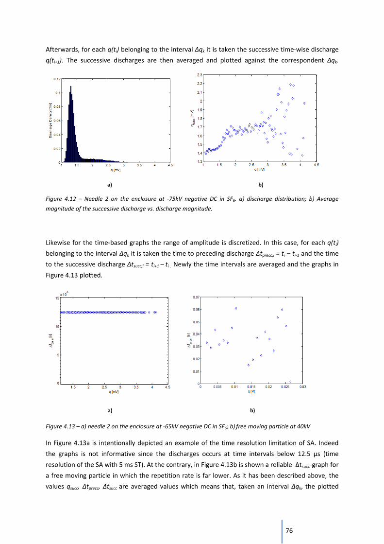
76
Afterwards, for each q(ti) belonging to the interval ∆qk it is taken the successive time-wise discharge q(ti+1). The successive discharges are then averaged and plotted against the correspondent ∆qk.
a) b)
Figure 4.12 – Needle 2 on the enclosure at -75kV negative DC in SF6. a) discharge distribution; b) Average magnitude of the successive discharge vs. discharge magnitude.
Likewise for the time-based graphs the range of amplitude is discretized. In this case, for each q(ti) belonging to the interval ∆qk it is taken the time to preceding discharge ∆tprecc,i = ti – ti-1 and the time to the successive discharge ∆tsucc,i = ti+1 – ti . Newly the time intervals are averaged and the graphs in Figure 4.13 plotted.
a) b)
Figure 4.13 – a) needle 2 on the enclosure at -65kV negative DC in SF6; b) free moving particle at 40kV
In Figure 4.13a is intentionally depicted an example of the time resolution limitation of SA. Indeed the graphs is not informative since the discharges occurs at time intervals below 12.5 μs (time resolution of the SA with 5 ms ST). At the contrary, in Figure 4.13b is shown a reliable ∆tsucc-graph for a free moving particle in which the repetition rate is far lower. As it has been described above, the values qsucc, ∆tprecc, ∆tsucc are averaged values which means that, taken an interval ∆qk, the plotted

77
value relative to ∆qk depend on the number of pulses np in the interval ∆qk and by the relative variance of the data σ. The number np turns to be dependent on the selected number of intervals n, that is selected by the user. Therefore, n should be adjusted in order to have a relative variance of the plotted point inferior to a certain value σerr (e.g. 10%). In Figure 4.14, we can see an example of the previously described qsucc – q graph improved with the σ. The graph presents a maximum variance σmax of 3.5% which fulfils the requirement σmax< σerr.
Figure 4.14 - qsucc – q graph extended with the information of the relative variance of each dot plotted.
The information provided by σ is also valuable to discard dots that are not informative. In fact, as we see in Figure 4.15, even if the variance of most of the dots is far below 10%, there is a dot in correspondence of 0.7 V that has σ equal to 33% which must be discarded. In this case, the number of interval n suits and does not need to be changed.
Figure 4.15 – The ∆tprecc – q graph extended with the information of the relative variance of each dot plotted. One dot presents a variance such large that must be discarded.
0.2 0.3 0.4 0.5 0.6 0.7 0.8 0.9 1
0.56
0.58
0.6
0.62
0.64
0.66
0.68
0.7
0.72
0.74
q [V]
q succ [V]
0.1 0.2 0.3 0.4 0.5 0.6 0.7 0.8 0.9 1-0.4
-0.3
-0.2
-0.1
0
0.1
0.2
0.3
0.4
q [V]
∆t prec [s
]

78
The graphs described in this paragraph represent a valuable tool. In Chapter 5 these graphs will be extensively used for the description and interpretation of the PD phenomena observed. We will notice that it is possible to extrapolate certain peculiar characteristic that render a possible distinction between negative corona, positive corona and free moving particle.

79
Chapter 5
In this chapter are presented the result of the measurement performed in the TU Delft High Voltage Laboratory. Each paragraph covers a defect, specifically, high voltage protrusion, low voltage protrusion and free moving particle. The measurement results are divided into AC voltage, Negative DC voltage and Positive DC voltage. At the end of each section a discussion is presented which focuses on the discharge physical mechanism and the comparison AC-DC.
5.1 High Voltage Protrusion
In order to create an high voltage protrusion, a needle has been placed on the conductor and fixed by means of conductive copper tape. The needle employed for the measurement are two:
• Needle 1 – copper, flat tip, tip radius 250 µm, length 30 mm; • Needle 2 – aluminium, sharp tip, tip radius 25 µm, length 30 mm.
The insulating gas used is humid air at 1 bar and SF6 at 1.1 bar.
5.1.1 AC Voltage
In Figure 5.1 are compared the trends of discharge magnitude and repetition rate per voltage period for Needle 2 in air on the left and in SF6 on the right. The trends refer to a corona discharge occurring in the negative voltage semi-wave, namely a negative corona. As the voltage rises, the repetition rate increases exponentially whereas the discharge magnitude tends to remain of the same magnitude. In both cases, as the repetition rate increases the discharge magnitude slightly decreases. The graphs show also the remarkable difference of discharge magnitude and repetition rate for the two gases. The SF6 molecules, strongly electronegative, capture the moving electrons so that the discharge extinguishes and its magnitude is limited. Furthermore, the SF6 ionic species generated during the
EXPERIMENTAL RESULTS
AND DISCUSSION

80
discharge have a larger molecular mass than those produced by a discharge in air, consequently the time to drift away and ignite another discharge is longer for SF6 than air. This explains the difference in repetition rate for the two gases.
Figure 5.1 - Trends of discharge magnitude 95% percentile and 20 ms period repetition rate at different voltage levels. a) Needle 2 in humid air at 1 bar; b) Needle 2 in SF6 at 1.1 bar.
The inception voltage for negative corona in SF6 at 1.1 bar is approximately twice than in air at 1 bar, confirming the Figure 2.2 in Chapter 2. Table 5.1 reports the value of the inception voltage for the two defects. The extinction voltage is omitted since it coincides with the inception voltage in all the cases.
Needle 1 Needle 2 Inception Voltage rms [kV] 1 bar Air
4.5 5.5
Inception Voltage rms [kV] 1.1 bar SF6
- 12
Table 5.1 - Comparison of the inception voltage for needle 1 and needle 2 for Air at 1 bar and SF6 at 1.1 bar.
Table 5.2 reports some of the negative corona PD patterns obtained for needle 2 in air. At first corona discharge appears at the instance of peak voltage and, as the voltage increases, it further develops occupying progressively the voltage wave. It has been also noticed that the discharge magnitude standard deviation diminishes at higher voltages. For each voltage level the discharge magnitude is relatively constant and it presents a flattening in conjunction with the peak voltage. Similar patterns are observed in SF6 and reported in Table 5.3. It was expected to find similar patterns in air and SF6 since, in both the electronegative gases, the space charge plays a major role.

81
Inception Voltage rms [kV] 5.3
QMax [pC] 22.4
QMean [pC] 19.3
Q StandardDeviation [pC] 0.609
Voltage rms [kV] 8.5
QMax [pC] 26.1
QMean [pC] 16.8 Q StandardDeviation [pC] 2.3
Voltage rms [kV] 12
QMax [pC] 20.1
QMean [pC] 15.6 Q StandardDeviation [pC] 1.348
Table 5.2 - Phase-resolved pattern for Needle 2 in air. For each voltage level are reported the characteristic parameters of the discharge magnitude. The data are acquired with an HFCT sensor connected to PDBaseII according IEC60270.
Inception Voltage rms [kV] 12
QMax95% [pC] 0.78
QMean [pC] 0.687
Q StandardDeviation [pC] 0.609
Voltage rms [kV] 20
QMax95% [pC] 0.878
QMean [pC] 0.678
Q StandardDeviation [pC] 0.115
Voltage rms [kV] 26
QMax95% [pC] 0.683
QMean [pC] 0.512
Q StandardDeviation [pC] 0.091
Table 5.3 - Phase-resolved pattern for Needle 2 in SF6. For each voltage level are reported the characteristic parameters of the discharge magnitude. The data are acquired with PDBaseII connected to the coupling capacitor according to IEC60270.

82
The discharge detection has been performed with both conventional method and UHF method: the internal antenna has been connected to PDBaseII, whereas another channel has been dedicated to the output of the coupling capacitor. In Figure 5.2 are shown the patterns at 45kV. It is noticeable that both patterns present two levels of discharge. On one hand, the lower discharge level has an higher repetition rate and it is flat over the voltage semi-wave. On the other hand, the higher discharges have a lower repetition rate and their magnitude is inversely proportional to the voltage applied as it is clearly visible in Figure 5.2a. Moreover, the higher discharges in the IEC 60270 pattern have somewhat twice the amplitude of the lower discharges while, in the UHF patterns, the lower discharges are many times smaller than the high discharges. Respectively, ~30mV and ~600mV. In the UHF method, the magnitude depends on several factors such as discharge mechanism, reflections and resonances. It may happen that the higher discharges causes EM waves whose resonances are better coupled with the antenna characteristic. In order to measure both discharge levels, the vertical scale has been enlarged resulting in a lower vertical resolution. As a consequence, positive corona has not been clearly detected with the UHF at the contrary of the IEC 60270 pattern where the latter is visible.
Figure 5.2 - Discharge pattern for discharge in SF6 at 1.1 bar and 45kV rms applied. a) output of the coupling capacitor according with IEC60270; b) UHF signal from the internal coupler.
Corona discharge appears also in the positive voltage semi-wave, at voltage somewhat higher than the negative corona inception voltage in SF6. This corona phenomenon, namely positive corona, presents a different pattern compared with the negative corona. As it is shown in Figure 5.3a, the discharge magnitude is locked with the voltage. However, referring to Figure 5.3b, at higher voltage levels the discharge pattern shifts to the right. The phenomenon is not totally understood. Regarding the repetition rate, the highest is recorded during the ascending and descending stage of the sinusoidal voltage, see blue and yellow points in the Figure 5.3.

83
a) b)
Figure 5.3- Phase-resolved pattern for Needle 2 in SF6 recorded with the output channel of Haefely detector connected to PDBaseII. a) 20kV rms; b) 30kV rms.
Similarly, in air, positive corona has been observed as shown in Figure 5.4. However, corona appears as long streamers of several thousand Pico coulomb magnitude and with a repetition rate of few discharges per period. The long streamers gets larger and larger as the voltage rises up to the breakdown voltage. The voltage has not been raised up to that extent.
a) b)
Figure 5.4 - Phase-resolved pattern for Needle 2 in air recorded with the HFCT sensor connected to PDBaseII according with IEC60270. a) Inception voltage at 31kV rms; b) 34.5kV rms.
5.1.2 Negative DC Voltage
In Table 5.4 are reported the measurements of the discharge magnitude for negative corona in air. The magnitude at the inception voltage is 55 pC and it decreases till a stable value of 28 pC at -21 kV. As the voltage increases stepwise the repetition rate boosts. The values of the repetition rate are omitted because the acquisition mode employed gave not reliable results (see Appendix C). In SF6 the negative corona magnitude was particularly low, below 1 pC, therefore the measurement were performed with the UHF antenna which provides the highest sensitivity. The summary of the measurement results are reported in Table 5.5. Also for the case of negative DC, the inception

84
voltage in SF6 is approximately twice than in air. Concerning the discharge magnitude, it has been noticed two clear discharge levels around 20 mV and 180 mV in the whole voltage range from -16 kV to -25 kV. The lower discharges have an higher repetition rate than the large discharges. This difference in the repetition rate gets larger as the voltage increases.
Needle 2 in AIR 1 bar Voltage [kV] Qmax95% [pC]
-8.5 55 -15 33 -21 28
Table 5.4 - Discharge magnitude trends of negative corona in air. Detection by means of HFCT sensor calibrated according IEC 60270.
Needle 2 in SF6 1.1 bar Voltage [kV] Qmin [mV] Qmax [mV] Repetition Rate [N/s]
-16 13 198 2785 -20 13 198 13971 -23 13 198 17514 -25 13 198 20677
Table 5.5 - Discharge magnitude trends of negative corona in SF6. Detection by means of UHF antenna connected to PDBaseII.
Two distinct discharge levels have been noticed also in air up to 20 kV. However, in air, the phenomenon was not so stable at prolonged voltage applied such as in SF6. Furthermore, at higher voltage the larger discharges disappeared giving way just to repetitive Trichel pulses as shown in Figure 5.5.
Figure 5.5 - Trichel pulses at 20 kV in air. Signal from Haefely unit connected to LaCroy fast digital oscilloscope.
Figure 5.6a represents the time-resolved pattern of negative corona at -23 kV in SF6. In the figure are clearly visible the two discharge levels mentioned above. The vertical scale has been intentionally kept at 200 mV in order to have an optimal vertical resolution. Out of the time-resolved pattern have been extrapolated relevant graphs for the characterization of the discharge.

85
a)
b)
c) d)
Figure 5.6 – a) Time-resolved pattern for negative corona at -23kV in SF6; b) mean successive discharge magnitude vs. discharge magnitude; c) mean time to the proceeding discharge vs. discharge magnitude; d) mean time to the successive discharge vs. discharge magnitude.

86
Looking at Figure 5.6b, mean successive discharge magnitude vs. discharge magnitude, three area are recognizable:
• From 10 mV to 80 mV, the successive discharges are in average of the same magnitude around 60 mV;
• From 80 mV 190 mV, the magnitude of the successive discharge is scattered due to the rare occurrence of discharge in the area;
• Above 190 mV, the successive discharge is in average a small discharge of 70 mV.
Figure 5.6c and 5.6d provides valuable information over the time between discharges. Two range are now analysed:
• From 10 mV to 180 mV, the discharges are equally spaced by time intervals of approximately 50 μs. Such regularity characterizes the Trichel pulses [21];
• Above 190 mV, the graphs clearly shows that for a 200 mV discharge the time for a successive is a short interval of 50 μs and it is proceeded by a longer interval of approximately 500 μs.
From the above consideration, we may infer that the discharge cycle begins with a large discharge followed by a series of smaller and evenly spaced Trichel pulses. Successively, the discharge extinguishes for an interval of approximately 500 μs and another discharge cycles starts.
Above 30 kV a new phenomenon has been observed: the repetition rate drastically drops till the extent in which almost no discharge is detectable. This may be addressed to the transition stage to pulseless corona. The case will be treated in the Discussion.
5.1.3 Positive DC Voltage
When positive DC voltage is applied the discharge generated by the protrusion on the conductor is called positive corona. From the measurement in air, reported in Tables 5.6 and 5.7, it is noticed that the discharge magnitude increases as the voltage is raised. We may notice the different discharge magnitude produced by the two needles due to the different tip shape. Indeed K. Asano et al. [46] noticed that the tip shape influence the discharge characteristic in positive corona since the avalanche starts by photo-emission away from the tip whose surrounding field is not strongly influenced by the space charge as in negative corona.
Needle 1 in AIR 1 bar Voltage [kV] Qmax95% [pC]
9 109 11 122 13 178 16 213 20 322
Table 5.6 - Discharge magnitude trends of positive corona in air. Detection by means of HFCT sensor calibrated according IEC60270.

87
Needle 2 in AIR 1 bar Voltage [kV] Qmax95% [pC]
10 56 15 109 20 106 25 119 30 147
Table 5.7 - Discharge magnitude trends of positive corona in air. Detection by means of HFCT sensor calibrated according IEC60270.
In Table 5.8 the measurement in SF6 confirmed the ascending trend of the discharge magnitude as well as the repetition rate. However, the results in SF6 have been hindered by the combination of a low discharge magnitude and the noise produced by the DC source. For this reason, the measurements were performed only with the UHF antenna which offers the best sensitivity.
Needle 2 in SF6 1.1 bar Voltage [kV] Qmax95% [mV] Repetition Rate [N/s]
35 5 3917 40 7 5640 45 10 11040
Table 5.8 - Discharge magnitude trends of positive corona in SF6. Detection by means of UHF antenna connected to PDBaseII.
In Figure 5.7 are presented the characteristic graphs of positive corona in air. Even though similar trends have been observed in SF6, it is not possible to derive such graphs because of the noise issue mentioned previously. In Figure 5.7b the distribution of the discharge magnitude presents a Gaussian-like distribution characteristic of corona discharge [11]. Indeed the mean discharge magnitude is around 25 mV irrespective of the previous discharge magnitude. However, the latter statement holds up to discharges of 40 mV; as it is shown in Figure 5.7c, beyond that magnitude level a discharge is in average followed by a likewise large discharge. Further, from Figure 5.7e shows that the time lag to the successive discharge is somewhat shorter for large discharges. In general, the time interval between discharges is relatively constant as in the case of negative corona. Summing up, the discharges occur at regular time intervals and with relatively the same discharge magnitude. Less frequently, rapid bursts of larger discharges occur as well.

88
a) b)
c)
d) e)
Figure 5.7- a) Time-resolved pattern for Needle 2 negative corona at 20kV in air; b) discharge magnitude distribution; c) mean successive discharge magnitude vs. discharge magnitude; d) mean time to the proceeding discharge vs. discharge magnitude; e) mean time to the successive discharge vs. discharge magnitude.

89
5.1.4 Discussion
In the previous paragraphs have been summarized the observations on the discharge behaviour for negative corona and positive corona under respectively negative and positive DC. The results obtained under AC voltage will also help to explain the physics of DC discharges.
The inception of negative corona under AC voltage and DC voltage is basically at the same voltage. In SF6, needle 2 causes negative corona inception at 16.9 kV (peak) and 16 kV negative DC. Indeed, the starting electron is generally originated by field emission from the cathode [4]. Once the minimum field required for the emission of an electron is achieved, the statistical time lag is generally several orders of magnitude lower than the variation of the AC instantaneous voltage [10], therefore AC voltage may be considered as DC voltage for that fraction of time. Similarly for positive corona in SF6 the inception voltage under AC voltage is at 36.5 kV (peak) and at 35 kV under positive DC voltage. However, in this case the starting electron is generally supplied from the gas by photoemission; this is why the inception voltage is higher than the one of negative corona. In general, it is possible to conclude that the inception of positive corona is always at an higher voltage which depend on the gas properties.
The discharge magnitude of negative corona in air does not present remarkable difference between AC and DC. In both voltage types the discharge was around 20 to 30 pC for all the voltage levels applied. Further, it has been noticed a slight reduction of the discharge magnitude and of its standard deviation as the voltage increases, both in DC and AC. The phenomenon is explained considering the role of the space charge generated by the electron avalanche: a negative cloud of space charge is formed around the tip that reduces the field in the ionization volume. This yields a reduction of the discharge magnitude and successively the extinguishment of discharges till the space charges drift away. The effect is called “corona shielding”. Therefore the first discharge in a space free gap is always larger than the successive discharges as it shown in Figure 5.8 where the first discharges in the negative voltage half-cycle are visibly larger.
Figure 5.8 - Phase-resolved pattern for Needle 2 in SF6 recorded with the coupling capacitor connected to PDBaseII according with IEC60270.
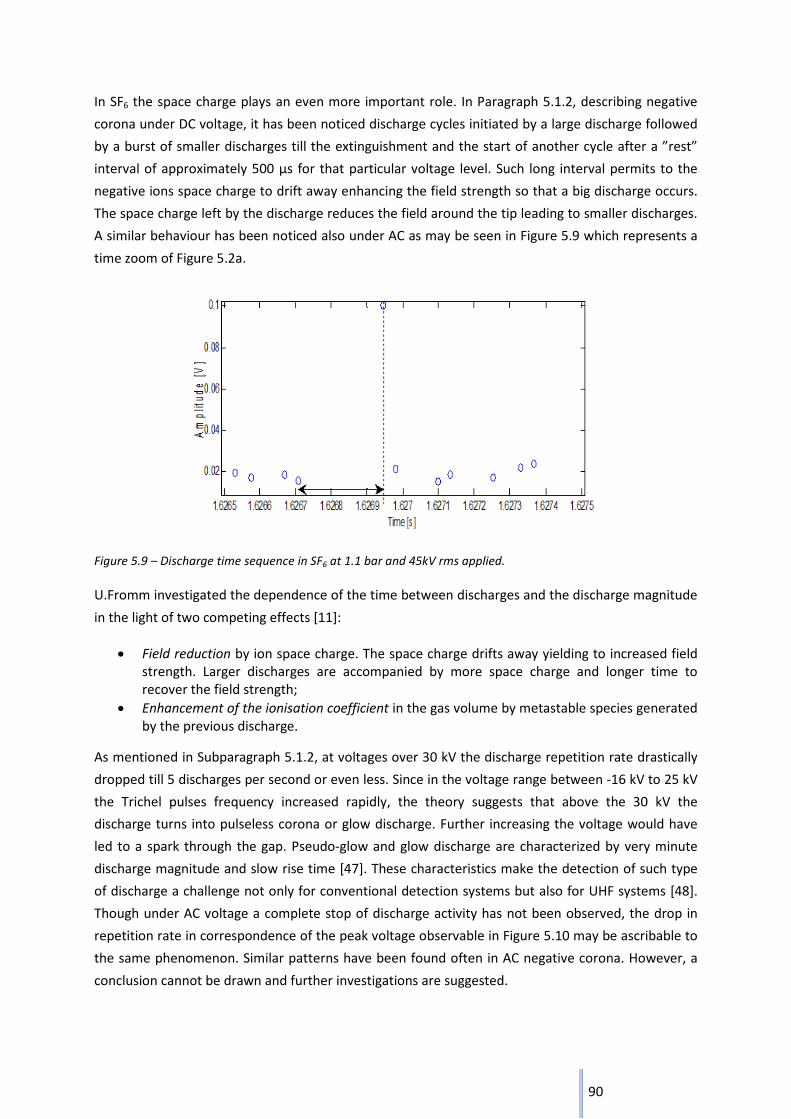
90
In SF6 the space charge plays an even more important role. In Paragraph 5.1.2, describing negative corona under DC voltage, it has been noticed discharge cycles initiated by a large discharge followed by a burst of smaller discharges till the extinguishment and the start of another cycle after a ”rest” interval of approximately 500 μs for that particular voltage level. Such long interval permits to the negative ions space charge to drift away enhancing the field strength so that a big discharge occurs. The space charge left by the discharge reduces the field around the tip leading to smaller discharges. A similar behaviour has been noticed also under AC as may be seen in Figure 5.9 which represents a time zoom of Figure 5.2a.
Figure 5.9 – Discharge time sequence in SF6 at 1.1 bar and 45kV rms applied.
U.Fromm investigated the dependence of the time between discharges and the discharge magnitude in the light of two competing effects [11]:
• Field reduction by ion space charge. The space charge drifts away yielding to increased field strength. Larger discharges are accompanied by more space charge and longer time to recover the field strength;
• Enhancement of the ionisation coefficient in the gas volume by metastable species generated by the previous discharge.
As mentioned in Subparagraph 5.1.2, at voltages over 30 kV the discharge repetition rate drastically dropped till 5 discharges per second or even less. Since in the voltage range between -16 kV to 25 kV the Trichel pulses frequency increased rapidly, the theory suggests that above the 30 kV the discharge turns into pulseless corona or glow discharge. Further increasing the voltage would have led to a spark through the gap. Pseudo-glow and glow discharge are characterized by very minute discharge magnitude and slow rise time [47]. These characteristics make the detection of such type of discharge a challenge not only for conventional detection systems but also for UHF systems [48]. Though under AC voltage a complete stop of discharge activity has not been observed, the drop in repetition rate in correspondence of the peak voltage observable in Figure 5.10 may be ascribable to the same phenomenon. Similar patterns have been found often in AC negative corona. However, a conclusion cannot be drawn and further investigations are suggested.

91
Figure 5.10 – Discharge pattern for discharge in SF6 at 1.1 bar and 50kV rms applied. Acquistion by means of UHF internal coupler connected to PDBaseII.
Turning the attention to positive corona, the discharge behaviour offers different characteristics from air to SF6 and partially from AC to DC. A general characteristic of positive corona is to generate discharge magnitude proportional to the voltage applied. This may be seen in the ascending magnitude trend of the tables of Paragraph 5.1.3 and by the ”vault-like” pattern both in air and SF6. In positive corona the starting electron originates by photoemission [5] in the gas. However, the starting electron must be inside the so-called critical volume, namely the region in which the ionization factor is higher than the attachment factor. Since the critical volume expands as the voltage increases, the electron avalanche may start from a further point. For the same reason positive corona discharge shows a larger standard deviation since it may develop everywhere within the critical volume.
5.2 Low Voltage Protrusion
The Low Voltage Protrusions investigated were three:
• Needle 1 – copper, flat tip, tip radius 250 µm, length 30 mm; • Needle 2 – aluminium, sharp tip, tip radius 25 µm, length 30 mm; • Needle 3 – aluminium, rounded tip, tip radius 500 µm, length 35 mm;
Needle 3 has been used only for the measurement in SF6. Since the other needles gave low discharge magnitude for negative corona, it has been assumed that a rounded needle would have generated a discharge magnitude large enough to be detected.
The insulating gas used is humid air at 1 bar and SF6 at 1.1 bar.

92
5.2.1 AC Voltage
Tables 5.9 and 5.10 report the measurements of needle 1 and needle 2 in air. The inception voltage for both the defects is around 16 kV rms which is not expected since the lower radius of curvature of needle 2 should have caused a lower inception voltage. Moreover, the discharge magnitudes are different, showing a higher level for needle 1 since it has a larger surface area subjected to a high field. Another reason of such discrepancy may be attributable to the different material employed since negative corona initially develops as a Townsend discharge mechanism whose source of secondary electrons is a cathode process [4]. However, the aluminium’s work function is 4.08 eV whereas the copper’s one is 4.7 eV which would suggest an opposite result. The cause of the magnitude difference may be addressed to diverse nature, among which:
• Tip shape even though the effect of space charge in the surrounding of the tip should attenuate the influence of the shape;
• Oxidation products deposited on the tip which may hinder the electrons release.
Nevertheless, the actual cause has not been further investigated being out of the scope of the project.
Needle 1 in AIR 1 bar Voltage rms [kV] Qmax95% [pC]
16.5 23 18 49 (Positive Corona) 23 50 (Positive Corona)
Table 5.9 - Discharge magnitude trends of corona in air with needle 1. Detection by means of HFCT sensor calibrated according IEC60270.
Needle 2 in AIR 1 bar Voltage rms [kV] Qmax95% [pC] Repetition Rate [N/20ms]
16 9 0.985 18 8.42 10 23 9.32 69 30 7.62 123
Table 5.10 - Discharge magnitude trends of corona in air with needle 2. Detection by means of HFCT sensor calibrated according IEC60270.
Needle 1 at 18 kV presented positive corona inception which has not been observed for needle 2 even at higher voltages. Table 5.11 shows the PDPR patterns at different voltage for Needle 2 in air. At low overvoltage, up to 18kV, the pattern is regular flat in correspondence of the peak voltage and it shows a slightly higher discharge magnitude for the first discharges of the cycle. The pattern at 18 kV is similar to the patterns of the same needle in the HV conductor.

93
Inception Voltage [kV] 16
QMax [pC] 12.1
QMean [pC] 7.7
QMin [pC] 5
Q StandardDeviation [pC] 0.898
Voltage [kV] 18
QMax [pC] 9.4
QMean [pC] 6.4
QMin [pC] 5
Q StandardDeviation [pC] 1.097
Voltage [kV] 23
QMax [pC] 12.5
QMean [pC] 6.9
QMin [pC] 3.2
Q StandardDeviation [pC] 1.376
Voltage [kV] 30
QMax [pC] 11.7
QMean [pC] 5.4
QMin [pC] 2.8
Q StandardDeviation [pC] 1.193
Table 5.11 - Phase-resolved pattern for Needle 2 in air. For each voltage level are reported the characteristic parameters of the discharge magnitude. The data are acquired with PDBaseII connected to the coupling capacitor according to IEC60270.

94
At 23 kV the pattern shows an higher discharge magnitude when the voltage approaches the peak value and the pattern seems to follow the voltage waveform in the descending stage. The effect of the voltage in the pattern is much more visible at 30 kV in which the discharge behaviour change drastically from a regular in the ascending phase of the voltage to a more scattered one once the voltage approaches the peak value and in the descending phase as well.
The tests in SF6 have been done with needle 3. The trends are displayed separately for negative corona and positive corona in Figure 5.11a and 5.11b respectively, while the patterns are shown in Table 5.12. Negative corona trends are very similar to those observed for needle 2 on the HV conductor (compare Figure 5.11a and Figure 5.1b). Instead, for the case of positive corona the discharge magnitude and the repetition rate increase with the voltage. It should be noticed that the repetition rate for positive corona is more than twice the repetition rate of negative corona.
Figure 5.11 - Trends of discharge magnitude 95% percentile and 20 ms period repetition rate at different voltage levels for needle 3 in SF6. a) trends for negative corona; b) trends for positive corona.
The PDPR patterns in Table 5.12 are combined with the discharge magnitude characteristic parameters divided for negative corona in red and positive corona in blue. Negative corona discharge holds approximately the same magnitude over the voltage range applied. However, the discharge pattern is different compared with negative corona generated from a protrusion in the HV conductor. Indeed the discharge magnitude follows the instantaneous voltage so that the pattern is phase locked. Further the first discharge of the voltage cycle is from two to four times larger than the successive discharges as in the case of the HV protrusion. Newly, positive corona discharge has a different behaviour from negative corona: the discharge magnitude increases at higher voltage levels. As in the case of HV protrusion, the maximum discharge occurs in the descending phase of the voltage wave. The interpretation of the above observations will be treated in the discussion.

95
Inception Voltage [kV] 32
QMax [pC] 2.44
QMean [pC] 0.954
QMin [pC] 0.498
Q StandardDeviation [pC] 0.412
Voltage [kV] 50
QMax [pC] 1 - 2 4.36 0.937
QMean [pC] 1 - 2 0.745 0.527
QMin [pC] 1 - 2 0.391 0.430
Q StandardDeviation [pC] 1 - 2
0.489 0.091
Voltage [kV] 60
QMax [pC] 1 - 2 4.062 2.422
QMean [pC] 1 - 2 0.788 0.831
QMin [pC] 1 - 2 0.430 0.469
Q StandardDeviation [pC] 1 - 2
0.365 0.249
Voltage [kV] 70
QMax [pC] 1 - 2 4.962 4.414
QMean [pC] 1 - 2 0.872 1.027
QMin [pC] 1 - 2 0.430 0.430
Q StandardDeviation [pC] 1 - 2
0.245 0.761
Table 5.12 - Phase-resolved pattern for Needle 3 in SF6. For each voltage level are reported the characteristic parameters of the discharge magnitude. The data are acquired with PDBaseII connected to the coupling capacitor according to IEC60270.

96
Concerning the detection systems employed, it has been noticed a lower sensitivity of the UHF system to detect positive corona. This occurred also for positive corona in the case of HV protrusion. The UHF system detected positive corona inception at 60 kV instead of its appearance at 50 kV with the conventional system shown in Table 5.12. As it is noticeable, comparing the two acquisitions at 70 kV in Figure 5.12 the UHF system misses the lower positive discharges yielding to a much lower repetition rate for positive corona in respect of negative corona. In Section 5.1 (Figure 5.2), it has already been discussed the difference in representing the discharge magnitude between conventional and UHF method. The present issue should be more investigated considering not only the EM wave propagation and the sensor characteristic but also the frequency shifter introduced between sensor and PDBaseII.
Figure 5.12 - Discharge pattern for discharge in SF6 at 1.1 bar and 70kV rms applied. a) UHF signal from the internal coupler; b) output of the coupling capacitor according with IEC60270.
5.5.2 Negative DC Voltage
Table 5.13 shows the trends of positive corona for needle 1. The inception voltage is roughly 3 times higher than the inception voltage of positive corona for the same needle on the HV conductor (positive DC voltage). The discharge magnitude as well as the repetition rate increase with the voltage.
Needle 1 in AIR 1 bar Voltage [kV] Qmax95% [pC]
-26 53 -30 66 -35 79 -40 92
Table 5.13 - Discharge magnitude trends of corona in air with needle 1. Detection by means of HFCT sensor calibrated according IEC60270.

97
Needle 2 in AIR 1 bar Voltage [kV] Qmax95% [pC]
-26.5 22 -28 27 -30 32
Table 5.14 – Discharge magnitude trends of corona in air with needle 2. Detection by means of HFCT sensor calibrated according IEC60270.
However, in air the discharge did not always show a regular behaviour:
• Low overvoltage (up to 5 kV over the inception voltage), the repetition rate increases as well as the discharge magnitude as we may expect for positive corona;
• Medium overvoltage (from 5 kV over the inception voltage to 50 kV), the repetition rate decreases as well as the discharge magnitude or even the discharge activity ceases;
• High overvoltage (above 50kV), discharge reappears with discharge magnitudes beyond 100 pC and in some cases nC.
PD behaviour presents a strong time dependency which is not always understandable. Figure 5.13 shows positive discharge caused by needle 1 in air at 50 kV over a time period of 35 minutes. We notice that the magnitude varies from 3000 pC to 100 pC over the acquisition time whereas the repetition rate has an inverse trend. This not constant trend may be addressed to a transition stage to long streamers.
Figure 5.13 - Discharge magnitude 95% percentile and repetition rate at 50 kV over 35 minutes. Needle 1 in air.

98
During other measurement with needle 2 the discharge activity ceases at 30 kV. Further increasing the voltage no discharge has been noticed. Once, the breakdown was reached around 85 kV without any preceding discharge detected.
Positive corona trend in SF6 is plotted in Figure 5.14. The discharge magnitude and repetition rate trends are very similar to positive corona under AC voltage (see Figure 5.11b).
Figure 5.14 - Trends of discharge magnitude 95% percentile and repetition rate at different voltages for needle 3 in SF6.
Figure 5.15 reports the characteristic graphs at -70 kV in SF6. The points of the successive discharge graph oscillate around a constant value of 12 mV similarly to the other graphs presented in the Chapter. Also the time graphs are constant around 450 μs which implies a certain regularity on the time between discharge regardless the discharge magnitude.
a)

99
b)
Figure 5.15 - a) Time-resolved pattern for positive corona at -70 kV in SF6; b) mean successive discharge magnitude vs. discharge magnitude; c) mean time to the preceding discharge vs. discharge magnitude; d) mean time to the successive discharge vs. discharge magnitude.
However, it has been noticed that the time between discharges at low magnitudes (5mV to 8mV) in some cases is much shorter as shown in Figure 5.16. Notice that if successive pulses appear in the same time window (5 μs) they are considered a single discharge by the software consequently the Figure 5.15c and 5.15d should show shorter Δtprec and Δtsucc around that signal amplitude.
Figure 5.16 – Examples of fast repetitive pulses at 70 kV. The acquisition time window is 5 μs.

100
5.2.3 Positive DC Voltage
When positive DC voltage is applied the needle on the enclosure causes negative corona discharge whose characteristic is a constant discharge magnitude at increasing voltages. As shown in Table 5.15 and 5.16, the discharge magnitude is relatively low, anyway lower than negative corona for HV protrusion (paragraph 5.1.2). The inception voltage is comparable to the inception voltage under AC voltage (22 kV peak voltage).
In some occasion the discharges showed a behaviour represented in Table 5.17. The PD activity begins with a large discharge followed by a burst of small discharges. The burst stops for a certain time interval in which no discharge occurs and successively a new cycle starts again with a large discharge. Increasing the voltage the so called dead time gets shorter till 50 kV where regularly recurring discharges appear. Unfortunately, no valuable acquisitions have been recorded for Needle 3 in SF6. Most likely the discharge magnitude was below the noise level so that no PD were detected up to 95 kV (the limit of the voltage source).
Needle 1 in AIR 1 bar Voltage [kV] Qmax95% [pC]
20 12 30 11 40 9 50 10
Table 5.15 - Discharge magnitude trends of corona in air with needle 1. Detection by means of HFCT sensor calibrated according IEC60270.
Needle 2 in AIR 1 bar Voltage [kV] Qmax95% [pC]
25 21 30 16 35 12 40 10 45 11
Table 5.16 - Discharge magnitude trends of corona in air with needle 2. Detection by means of HFCT sensor calibrated according IEC60270.

101
Voltage PDBaseII acquisition window LaCroy Oscilloscope
30 kV
40 kV
50kV
Table 5.17 – Comparison of PDBaseII acquisition window and the oscilloscope screenshot at 30 kV, 40 kV and 50 kV. Needle 2 in air.

102
5.2.4 Discussion
In the previous paragraphs we went through the behaviour of negative and positive corona generated by a protrusion on the GIS enclosure. From the measurement several common characteristics have been observed between protrusion on the HV conductor and on the enclosure. However, certain characteristic differences have been observed as well. In this paragraph the measurements are discussed in the light of the consideration drawn for the HV protrusion.
Table 5.18 summarizes the inception voltage for the protrusion on the enclosure. The inception in SF6 occurs at approximately two times the voltage in humid air. The result is in accordance with Figure 2.2 which gives the inception voltages for Air and SF6, after all this it has been already noticed for the inception voltages in the HV protrusion. Moreover, if the AC peak voltage is considered, the inception at AC and DC are approximately the same. Another comparison may be done between inception voltages at the HV conductor and at the enclosure. In fact, the inception at the enclosure occurs at approximately 2.8 – 3 times the inception at HV conductor since that value corresponds to the field ratio between the position of the needle tip on the two locations.
Inception Voltages
Humid Air – 1 bar SF6 – 1.1 bar
AC rms [kV]
16.5 (negative corona) - Needle 1
18 (positive corona) - Needle 1
16 (negative corona) - Needle 2
32 (negative corona) – Needle 3
50 (positive corona) – Needle 3
DC- [kV] 26 (positive corona) - Needle 1
26.5 (positive corona) - Needle 2 60 (positive corona) – Needle 3
DC+ [kV] 20 (negative corona) - Needle 1
25 (negative corona) - Needle 2 No detection
Table 5.18 – Summary of the inception voltage for the protrusion on the enclosure.
In the case of SF6 under AC voltage, a different pattern for negative corona has been noticed. The magnitude of negative corona in the enclosure looks voltage phase locked which resembles a positive corona pattern. However, addressing our attention to the repetition rate, we notice that the repetition rate for negative corona in the enclosure goes up to 18 discharges/period at 70 kV whereas on the HV conductor is 120 discharges/period at 26 kV. Since the two voltages correspond to the same background field at the tip of the needle we may infer that the repetition rate is lower for a protrusion on the enclosure. The reason of this difference is due to the different field configuration at the two positions. In fact, the field gradient at the enclosure is less steep consequently the space charge has a lower drift velocity. The next discharge occurs when the space charge is far enough to restore the field necessary to ignite another avalahance. However, due to the low repetition rate, the space charge around the tip is not considerable so that the next discharge will have a magnitude somewhat proportional to the voltage.

103
Now we call our attention to positive corona patterns in SF6 under AC voltage. The patterns in Table 5.12 show larger discharges at increasing voltages. The highest PD occurrence is at the peak voltage (blue points) while the largest discharge magnitude is in the descending phase of the voltage wave. The phenomenon is explicable in the light of the positive corona theory [5]. The positive space charge generated by the first discharge, on one hand, reduces the field at the tip and, on the other hand, enhances the field toward the electrode. So that, during the drift, the positive space charge extends the critical volume yielding to larger discharges. Moreover, the discharge process releases photons that contribute to the ionization of the gas molecules. In this way secondary electrons are quickly available to start another discharge which means a higher repetition rate compared with negative corona whose secondary electrons are mainly supplied by a cathode process.
5.3 Free Moving Particle
In this Section are reported the PD measurements generated by a free moving particle placed on the enclosure of the GIS, as depicted in Figure 5.17. The particle under test has the following characteristics:
• Aluminium curly-shaped particle; • 10 mm long and 2 mm wide; • 8 mg weight.
Figure 5.17 - The particle lays on the enclosure of the GIS. It is tied by means of the red cotton thread to the enclosure.
The particle has been selected over several other differently shaped particles since it showed the lowest lift-off voltage in order to satisfy the maximum voltage applicable by the DC source (100 kV). Eventually, the particle is tied to the enclosure by means of a cotton thread in order to avoid the particle escape from the grounded section of the GIS. In fact, under DC voltage the particle is subjected to tangential forces when it touches the HV conductor. However, the thread influences both the motion and the PD behaviour. Other solutions without thread have been tried, among others, a plexiglas cylinder surrounding the particle with the side facing the HV conductor opened to

104
permit the particle hits against the conductor. Nonetheless, the best solution has been identified utilizing the thread.
Since the levitation is an electric field driven phenomena, it is expected that the gas type does not influence the particle motion [49]. Therefore, either CO2, atmospheric air or SF6 behave similarly unless any corona and space charge distribution in the gas is present. The experiments have been carried out in the GIS filled with CO2 at 4 bar.
5.3.1 Particle Motion
A recurrent cause of failure in GIS is a metallic free moving particle. Several studies [49], [50], [51] have investigated the effect of free moving particle on the gas dielectric strength. A free moving particle in contact with the enclosure of an energized GIS acquires an induced surface charge whose interaction with the background electric field exerts a columbic force on the particle itself. The particle lifts off as soon as the columbic force exceeds the gravitational force and it accelerates toward the electrode. The dynamic equation of the particle motion is described by the following equation:
𝑚�⃗� + �⃗�𝐶𝑜𝑢𝑙𝑜𝑚𝑏 + �⃗�𝐷𝑟𝑎𝑔 + �⃗�𝐺𝑟𝑎𝑣 = 0
The particle shape and size influence very much the charge accumulation and, consequently, the lift-off voltage and the electric field distortion. Ultimately shape and size affects differently the breakdown strength of the system. Anis and Srivastava [52] give a detailed analysis of the influence of the particle shape on the field distortion and the surface charge distribution for a filamentary and spherical particle. The mentioned particle shapes represent the two extremes in between of which we may derive all the other particle shapes.
The presence of a dielectric coating impedes the particle movement in two instances [49]:
• the dielectric coating interposed between particle and metallic enclosure does not permit the charge exchange when the charged particle hits the electrode;
• when the particle lays on the enclosure, a dipole force opposes the HV electrode-directed coulombic force.
However, in case of spacer proximity, the presence of a particle is more dangerous than further away. Refer to Chapter 2, particle on the spacer, for further details.
The particle dynamics are governed by the induced net charge deposited on its surface which is in turn dependent on the voltage magnitude at the lift off instant (background electric field), and by the particle shape (distorted electric field). Therefore, it is expected that particle trajectory is phase-locked under AC whereas it will be constantly accelerated under DC voltage.
Both for DC and AC voltage applied the particle motion and consequently the discharge generated presents different behaviour at low voltage (i.e. around lift off voltage) and at high voltage (i.e. more than twice the lift off voltage).

105
At low AC voltage Meijer [53] identified three stages in the particle movement:
1. Shuffling particle: really slow particle movement which caused contact-noise-like PD activity; 2. Moving particle: particle starts moving, accompanied with higher PD activity; 3. Jumping particle: particle starts jump and it may be airborne for more than one voltage cycle.
At DC voltage particle shuffling and moving are rarely seen. The charged particle lifts off and it is driven through the gas gap till it collides with the HV electrode, where it is oppositely charged and pushed back toward the enclosure; a bouncing motion initiates in which the particle carries charge from the enclosure to the HV electrode and then opposite charge back to the enclosure. In case of wire particle Cooke et al. [49] observed that it may move to a vertical standing position before it lifts.
In Figure 5.18 are reported the results of Cooke et al. [49] of the lift off voltage for wire particles and sphere particle at DC and AC voltage. As it may be noticed, there is not a relevant difference between AC and DC lift-off field. The scatter even between the same type of particle may be caused by the influence of the particle position and orientation on the enclosure.
Figure 5.18 - Normalized lift off field of wire and sphere particles under DC and AC voltage. The test is carried on a 250/76 mm coaxial electrodes system filled with SF6 and N2 [49].
At higher field intensity several authors [50] [49] [52] report in-flight corona. The loss of net charge during the flight toward the electrode causes a lower electric force exerted on the particle and its

106
deceleration. Under DC voltage it is visible a deceleration and even a drop of the particle due to total discharge [54]. Holmberg et al. [55] observed also multiple particle discharges occur at 90° or 270° when the field is at the peak. The space charge cloud generated by in-flight corona may have an influence in the reduction of the breakdown voltage as it is observed in [49] comparing the breakdown voltage of a wire particle and a spherical one which produces less corona discharge.
5.3.2 AC Voltage
In Figure 5.19 are shown the characteristic trends of discharge magnitude and repetition rate for a jumping particle. The repetition rate maintains a constant value of approximately 3 discharges\period over the whole voltage range tested. Therefore we can conclude:
1. The particle does not stay airborne for more than one period; 2. The particle does not experience considerable in-flight corona.
Vice versa the discharge magnitude linearly increases as the voltage rises since, as explained in the previous paragraph, the PD magnitude is related to the induced surface charge on the particle.
Figure 5.19 - Trends of discharge magnitude 95% percentile and 20 ms period repetition rate at different voltage levels for curly particle in CO2 at 4 bar.
The corresponding PRPD pattern of the trends above are shown in Table 5.19.

107
Table 5.19 - Phase-resolved pattern for curly particle in CO2. For each voltage level are reported the characteristic parameters of the discharge magnitude. The data are acquired with the HFCT sensor connected to PDBaseII and calibrated according IEC60270.
The PDPR pattern above are interpreted at the light of the consideration of Schlemper-Feser [56] and Wohlmuth [57] who claim that the PD impulse generated by a jumping particle is the difference between the induced charge before and after the impact of the particle with the enclosure. The net
Voltage [kV] 45
QMax [pC] 1 2 72.1 69.7
QMean [pC] 1 2 30.5 28.2
QMin [pC] 1 2 16.8 14.4
Q StandardDeviation [pC] 1 2
10.626 12.901
Voltage [kV] 55
QMax [pC] 1 2 93.7 86.5
QMean [pC] 1 2 33.5 31.4
QMin [pC] 1 2 16.8 14.4
Q StandardDeviation [pC] 1 2
15.584 17.667
Voltage [kV] 65
QMax [pC] 1 2 115.3 103.3
QMean [pC] 1 2 35.6 33.5
QMin [pC] 1 2 16.8 14.4
Q StandardDeviation [pC] 1 2
15.584 17.667
Voltage [kV] 75
QMax [pC] 1 2 136.9 115.3
QMean [pC] 1 2 36.8 32.3
QMin [pC] 1 2 16.8 14.4
Q StandardDeviation [pC] 1 2
25.645 23.512
Voltage [kV] 85
QMax [pC] 1 2 156.1 129.7
QMean [pC] 1 2 37.3 34.7
QMin [pC] 1 2 16.8 14.4
Q StandardDeviation [pC] 1 2
26.966 26.023

108
charge after the impact is proportional to the instantaneous voltage at the impact instant while the net charge before impact is proportional to the instantaneous voltage at the preceding impact. This is graphically depicted in Figure 5.21.
Figure 5.21 - The discharge impulses are the difference between net discharge stored in the particle before and after the impact with the enclosure [55].
As a consequence, if a random particle movement is assumed, the PD pattern in AC is the envelope of the sinusoidal voltage, as it is shown in Table 5.19. The trajectory of charged particle is voltage phase-locked; therefore the discharges are not uniformly distributed over the 360° period [56]. However, the probability of particle impact with the enclosure is higher in proximity of the zero-crossing since its speed toward the enclosure is maximum [56]. In particular, for negative charged particles the highest probability is around 0° while for positive charge particle is around 180°. This explains why positive discharges are denser around 180°. The PDPR patterns are symmetric over the whole voltage range tested. However, in case of in-flight corona the particle would lose part of its charge during the flight so that the pattern would present lower discharge magnitudes.
Preceding the jumping phase, the particle may shuffle or slowly move producing a characteristic contact-noise-like pattern shown in Figure 5.22. Such a pattern has been observed also when the particles get welded on the enclosure at voltage level in which it should have jumped.
Figure 5.22 – PDPR pattern of the curly particle in CO2 during the shuffling stage. The pattern resembles contact-noise.

109
5.3.3 DC Voltage
Under DC voltage the particle dynamics does not vary considerably between positive or negative polarity. The particle lifts when the coulombic force exerted is high enough to win the opposite directed gravitational force and it travels toward the cathode (Figure 19a). Therefore, it is not observed a jumping stage, unlike under AC voltage, but a continuous bouncing trajectory between cathode and enclosure and vice versa, as shown in Figure 5.23. When the charged particle is in proximity of the electrode, the electric field is enhanced which may cause the discharge inception still in the airborne. At the contact instance the particle discharges its accumulated charge (Figure 23b) and gets charged of opposite polarity. Then it drops back to the enclosure, pushed by the electric force and the gravitational force which are now equally directed (Figure 23c). Again at the contact with the enclosure the charge will flow to the ground (Figure 23d) and another cycle starts.
Figure 5.23 – Dynamics of a metallic particle subjected to an electric field under DC voltage.
The discharge magnitude depends on the induced charge at the moment in which the particle get detached by the electrodes. As already mentioned, the induced charge is proportional to the surrounding electric field. Therefore the discharge magnitude will present two distinct levels whose intensity is proportional to the field at the HV electrode and that at the enclosure, as it is shown in the Time-Resolved Pattern in Figure 5.24. In the pattern we notice that the discharge are of the same polarity. In fact, a negative charge flowing into the HV electrode and a positive charge flowing to the ground are discharges of the same polarity for the detector.
In Figure 5.20a are visible three discharge levels at 65 kV:
• q < 5mV • 5mV < q < 10mV • 15mV < q < 20 mV

110
These discharge levels will be treated separately in the light of the characteristic graphs shown in Figure 5.24.
Figure 5.24 - a) Time-resolved pattern of jumping particle in SF6; b) mean successive discharge magnitude vs. discharge magnitude; c) mean time to the preceding discharge vs. discharge magnitude; d) mean time to the successive discharge vs. discharge magnitude.
a)
b)
c)
d)

111
Discharge magnitude: q < 5mV
Discharges below 5mV occur with the highest repetition rate. The successive discharge is in average of the same magnitude and the time to the preceding discharge is the lowest in the pattern being in average around 10 ms. These discharges are an example of in-flight corona and they occur when the negatively charged particle is in proximity of the HV conductor, since the electric field is enhanced in the region between particle tip and conductor. Furthermore, when the particle touches either the conductor or the enclosure multiple discharges have been observed by Holmberg [55]. An example of these discharges is shown in Figure 5.25.
Figure 5.25 – Two fast repetitive discharges acquired in 5 µs time window.
Discharge magnitude: 5mV < q < 10mV
In this range, the magnitude of the successive discharge is around 20 mV, the highest in the pattern. Concerning the time between discharge, we notice that the preceding discharge occurs on average at 40 ms whereas the successive is after 100 ms. These discharges are those caused by the particle contact with the enclosure since the particle falling time is lower than the lifting time.
Discharge magnitude: 15mV < q < 20 mV
The successive discharge is in average a low discharge of 3 mV whereas the time between discharges is the specular of the previous case: the preceding discharge occurs on average at 100 ms whereas the successive is after 40 ms. Therefore these are the discharges caused by the hit with HV conductor.
In Figure 5.26 it is interesting to compare the discharge density distribution produced by a bouncing particle at 65 kV and 40 kV. At 40 kV the in-flight corona and the multiple contact discharges are less frequent which turns in evenly distributed discharges into two levels. At the contrary, at 65 kV the lower discharges are visibly more frequent.

112
Figure 5.26 – On the top, discharge magnitude distribution at 40 kV; On the bottom, discharge magnitude distribution at 65 kV;

113
5.3.4 Discussion
It should be kept in mind that the experiments have been performed with a particle tied by means of a cotton thread whose effect is not negligible. Two factors are affecting the particle’s motion:
• The weight of the thread even if several time lower that the particle’s one; • The induced charge on the thread.
Regarding the lift-off voltage, these two factors are opposed. Moreover, it is believed that the thread may influence also the PD behaviour.
In Figure 5.27 are reported the lift-off voltages under AC, positive DC and negative DC. As it is mentioned previously in paragraph 5.3.1, the lift-off voltage does not vary considerably for AC and DC. In this case, it appears more correct to compare the AC rms voltage with the DC value. In fact, even if at the peak the Coulomb force would exceed the gravitational the particle does not lift because of the inertia and the short time in which the peak holds.
Though the lift-off voltages are comparable, it is shown also a large variance. In fact, the Coulomb force, responsible of the particle levitation, depends on the induced surface charge deposited on the particle. Therefore, it turns that the orientation of the particle determines the induced surface charge and consequently the lift-off voltage since the electric field distortion varies with the orientation.
Figure 5.27 – Lift-off voltages for AC, positive DC and negative DC. The values plotted for AC are rms.

114
Surface charge computation with Finite Element Method (FEM) Simulation.
A simulation with the FEM software COMSOL has been carried out to evaluate the influence of the particle position and orientation on the induced surface net charge. The geometrical model is composed by a coaxial geometry and by a helicoidal particle. The coaxial geometry is long 5 m which permits to obtain a uniform field distribution in its center where the helicoidal particle is placed. The helicoidal particle is long 10 mm as the real particle and the radius is 5 mm which approximates the not constant radius of the real particle. The particle material is aluminium. The coaxial geometry has been filled with CO2 at 1 bar. The electrostatic simulation has been performed with a 40 kV positive DC applied at the HV conductor.
The COMSOL model is based on the following assumptions:
• The particle in the real GIS is placed in proximity to the end of the conductor; this adds the influence of the field distortion due to the edge effect. It is assumed that such edge effect rather affects the particle motion dynamic than the surface charge induced;
• Due to the complex geometry of the real particle the simulated geometry has been simplified to a helicoidal cylinder. However, the interest is addressed to the variations in charge induced rather than the actual surface charge value;
• Characteristic parameters such as pressure and particle weight do not influence the electrostatic simulation.
In Table 5.20 are shown the results of the simulation and it appears that between two positions there is a maximum variation of surface charge of approximately 10%. The surface charge is proportional to the electric field exerted as we see from the difference of the charge on the enclosure and in contact with the conductor.
Position Orientation Surface Charge [nC]
Enclosure
0.833
Enclosure
0.883
Enclosure
0.921

115
Position Orientation Surface Charge [nC]
Conductor
3.683
Conductor
3.062
Conductor
4.079
Table 5.20 – Simulation results of the surface charge accumulated on the particle in several positions and orientations.
PD features.
The PD waveform has not appeared different from AC to DC. In both cases a peculiar feature is present that has not been noticed in the case of corona PD: a fast transient in the second oscillation of the wave. Such a transient, shown in Figure 5.28, may be addressed to the charging and discharging process that occurs when the particle touch a conductive part. This may be a characteristic that can be used for the recognition of the discharge.
Figure 5.28 – PD signal waveform generated by a jumping particle. The red circle encloses a fast transient characteristic of these PDs.
What may be used for the recognition of the discharge are the graphs ∆tprecc – q and ∆tsucc – q which are different from those obtained from corona discharge. In fact, in Figure 5.29 we can see two

116
specular clusters: the red cluster which represents the small discharge magnitudes and the green one for the big magnitudes. Clearly the red cluster represents the hit of the particle to the enclosure since the time of the preceding discharge is shorter than the time to the successive discharge (particle hits the conductor). In other words, the time required to the particle to cover the distance conductor-enclosure is shorter than the time for enclosure-conductor since, in the first case, not only the gravitational force is direct downwards but also the Coulomb force is from three to four times bigger being directly proportional to the surface charge on the particle.
Figure 5.29 - ∆tprecc – q and ∆tsucc – q graphs of a jumping particle. In red and green boxes are enclosed the points corresponding respectively to the particle’s hit to the enclosure and to the conductor.

117
Chapter 6
In this Chapter are presented the main conclusions of the research regarding the PD physics and the recognition of the discharge. Moreover, are also suggested possible paths to continue and deepen the research.
6.1 Conclusions
The main results of the research are listed here below. The conclusions are separated in three areas: 1 - PD mechanism focused on the comparison AC – DC; 2 - detection systems deals with the IEC 60270 and UHF method; 3 - PD recognition under DC voltage.
PD mechanism - AC and DC
• The inception voltage for negative corona does not present relevant differences between AC (peak value) and DC voltage. In fact, once the minimum field required for the emission of an electron is achieved, the statistical time lag is generally several order of magnitude lower than the variation of the AC instantaneous voltage, therefore AC voltage may be considered as DC voltage for that fraction of time. The inception voltage for positive corona is always somewhat higher than the one for negative corona since the starting electron is originated in the gas away from the protrusion tip. In all the cases the extinction voltage corresponds with the inception voltage. For the case of free moving particle, again the lift-off voltages are comparable for DC and AC. However, the lift-off voltage presents a large scatter since it depends also on the position and orientation of the particle. Regarding the extinction voltage, it has been noticed an hysteresis: once the particle starts to jump it stops at a lower voltage. Sometimes, it may happen that the particle gets welded to both at enclosure and to the conductor (under DC negative).
CONCLUSIONS AND RECOMMENDATIONS FOR FUTURE
RESEARCH

118
• The trends of PD magnitude and repetition rate at increasing voltage are similar between AC and DC. For negative corona, both AC and DC present a stable PD magnitude level over the voltage range tested and an exponentially increasing repetition rate. The PD magnitude does not increase because of the “corona shielding effect” caused by the space charge produced subsequently a PD. Instead, for positive corona, the PD magnitude is proportional to the voltage applied since the ionization volume enlarges proportionally to the electric field.
• Often it has been observed a relation between PD magnitude and time between discharges under DC. The “memory effect” is due to the space charge; therefore, the memory is lost if the time elapsed between two discharges is larger than the time required to the space charge to drift away. A further element that contributes to the memory effect is the enhancement of the ionisation coefficient by metastable species generated by the previous discharge; in fact, larger discharges generates metastables that cause an increase of the ionisation coefficient.
• Under certain conditions the PD activity ceases at a certain voltage level. The phenomenon is believed to be caused by pulseless corona or glow discharge which presents a DC offset and a rising time on the range of microseconds. These characteristic makes this discharge type detection a challenge both for IEC 60270 and UHF method. The discharge discontinuance has been observed in two cases: HV protrusion under negative DC (negative corona) in SF6 and LV protrusion under negative DC (positive corona) in Air.
• The motion of a free moving particle varies between AC and DC. Under DC voltage the particle, once it lifts, commences a continuous bounce from enclosure to conductor and back. At the contrary of particle under AC voltage, under DC it has not been observed a shuffling stage in which PDs are produced. At the moment of the hit against the HV conductor the particle is subjected to a tangential force which drives the particle away. Further, under negative DC the particle tends to get attached to the HV conductor.
Detection systems – IEC 60270 and UHF method
• Under DC the time resolution of the detection system is of fundamental importance, especially with high repetition rate. Generally, a wide band system offers a better time resolution than a narrow band system. The best resolution of 1 µs has been offered by PDBaseII in wideband mode. In addition to the time resolution, the acquisition dead time affects the results obtained. The acquisition dead time for the system SA-laptop is particularly long due to the data transfer via PCMCIA – PGIB link.
• The best sensitivity has been achieved with the UHF method. The system composed by UHF antenna connected to PDBaseII was able to measure PD magnitudes below 1 pC.
• The UHF signal amplitude is surely related to the PD magnitude but it also depends on several factors among which the resonances, the location of the defect on respect of the antenna and the defect type. Moreover, it has been described in Paragraph 3.2.1, that the steepness of the PD pulse influences both the frequency content of the signal and the energy content of the frequency spectrum. For this reasons the amplitude of the UHF signal cannot be directly related to the PD magnitude.

119
Recognition of PD under DC
• From the time-resolved pattern are derived the characteristic graphs qsucc – q, ∆tprecc – q, ∆tsucc
– q and the distribution of q. These graphs are valuable visual tools to understand the PD sequence. From these graphs it is possible to differentiate protrusion from free moving particle. However, it is not easily recognizable a protrusion on the enclosure from a protrusion on the HV conductor. Furthermore, negative and positive corona presents different behaviour at low and high overvoltage, this introduces another problem for an online application since it is not known a priori the evolution of the PDs.
• Since the characteristic graphs are based on average of PDs magnitude and inter-time, they are improved by the information over the variance of the data. In this way, the information provided by the graphs is properly evaluated.
• By using only the information provided in the time-resolved pattern it is not possible to recognize multiple defects nor effectively denoise the signal.
• The spectrum analyser loses the time-domain information of the signal, namely the signal waveform. This introduces limitations to the capability of the system to recognize multiple defects and to separate the noise from the signal. With other systems (e.g. TF map) based on the signal waveform better performance can be achieved.
6.2 Recommendations for future research
In this section a few recommendations for future research are given:
• The transition from Trichel pulses to glow discharge should be further investigated since it is the stage preceding the breakdown. In addition, the glow discharge is hardly detectable by the employed detection systems. Future research should be addressed to alternative detection systems keeping in mind their possible applicability for online detection.
• “DC voltage does not exist” (H.F.Kreuger). In fact, HVDC voltage is produced by switching converter that causes voltage steps and transients. It may be of interest the research of the effect of such steep voltage steps on the generation of PDs.
• It has been noticed a certain time dependency of corona magnitude and repetition rate over long time period (e.g. 30 minutes) with DC voltage applied. The PD evolution over the time may be of interest for future research.
• Several recognition techniques based on the PD wave form should be investigated. • The behaviour of the free moving particle should be further researched leaving the particle
free to move rather than tied with a thread. In order to do so, a dedicated measurement set-up should be built.
• The project has to be completed testing other defects namely, particle on the spacer, void in the insulator and floating electrode.

120
Appendix A
A.1 Introduction
For AC, the classification of PD data is based on the discharge magnitude q and the phase angle φ in correspondence of which the discharge occurs. Whereas, for DC, the reference of the phase angle it is not applicable, therefore, besides the discharge magnitude q, the other parameter is the time between discharges Δt1. For this reason, the accuracy of the measuring devices in detecting successive discharge are of importance for the classification of the discharge under DC.
The PD data accuracy is in general hindered by two measuring device errors:
1. The superposition error is caused by the overlapping of transient output pulse responses when the time interval between input current pulses is less than the duration of a single output response pulse. Superposition errors may be subtractive or additive depending on the discharge repetition rate. In this view, it is important to define the pulse resolution time Tr which is the shortest time interval between two consecutive input pulses of same shape, polarity and charge magnitude for which the peak value of the resulting response will change by not more than 10% of that for a single pulse2. Broadly speaking, Wide Band (WB) detection systems have a shorter Tr than Narrow Band (NB) ones.
2. The integration error occurs when the upper frequency limit of the PD current pulse is lower than the upper cut-off frequency of a WB system or lower than the mid-band frequency of NB system3. Figure A.1 shows the correct relationship between the bandwidth of measuring device, PD pulse and calibrator pulse.
1 P. Morshuis, M. Jeroense and J. Beyer, “Partial Discharges Part XXIV: The analysis of PD in HVDC Equipment,” IEEE Electrical Insulation Magazine, vol. 13, no. 2, pp. 6-16, 1997. 2,3 E. Kuffel, W. S. Zaengl and J. Kuffel, High Voltage Engineering: Fundamentals, Newnes, 2000.
REPETITION RATE CHECK

121
Figure A.1 - Correct relationship between bandwidth: A - band-pass filter of the measuring system; B - amplitude frequency spectrum of the PD pulse; C - amplitude frequency spectrum of the calibrator pulse4.
The purpose of this report is to determine the capabilities and limitations of the Spectrum Analyzer (SA) and PDBaseII in the determination of the repetition rate. The SA is operated in zero-span mode.
A.2 Test Procedure
The devices investigated are a SA Agilent E4403B and the PD detector Techimp PDBaseII. Pulses have been injected at the input terminal of these devices by a Tabor Electronics WW1281 waveform – pulse generator with 1.2 GS/s.
The repetition rate check is composed by three tests
1. Bipolar pulses test: The PG is set to square-wave mode and a capacitance is connected in series to it, as shown in Figure A.2. Therefore, at each voltage step a fast pulse is generated of positive polarity or negative if the voltage increases or decreases respectively, as it is shown in Figure A.3. Adjusting the width of the square wave the distance of two successive pulses is varied. The purposes of the test is to determine the shortest time between pulses of different polarity; the divergence in measured amplitude of different polarity signals; the pulse recognition during superimposition error.
4 IEC Standard 60270 (III Edition) - Partial Discharge Measurments, 2001.

122
Figure A.2 – Schematics of the circuit to produce two successive pulses spaced out by an adjustable time interval
Figure A.3 – A pulse is created by the step voltage. Each pair of pulses are spaced out by a fixed time of 10 ms which has been kept constant during the tests.
2. Burst pulses test: the Pulse Generator (PG) is connected to the input terminal of the device under test. Then, the PG is set in burst mode, namely a mode to produce n successive pulses spaced out by a fixed Δt which is varied in order to determine the limitations of the devices. Indeed, for each Δt tested, the number of detected pulses, the measured Δt and the measured signal amplitude are calculated. The purposes of the test is to determine the time resolution of the measuring device; the influence of measuring system (hardware and software) on the pulse detection; the detectability of short duration phenomena.
3. Continuous train of pulses test: The PG is set to continuous mode and the time between pulses is adjusted. For each time interval Δt tested, the measured Δt and the measured signal amplitude are calculated. The purposes of the test are the same of the burst pulse test whose results comparison is necessary for the obtainment of such aims.

123
The discharge pulses are influenced by several factors, among others the gas pressure, the gas species and the discharge type itself. In fact, the pulse rise time is related to the extinction time of the electrons avalanche, whereas the fall time correlates with the drift of the space charge after the avalanche extinction5. Typical values for SF6 at 0.1 MPa lay in the range of 5 ns to 0.5 ns for the rise time and 10 ns to 3 ns for the fall time6. In Figure A.4, the pulse shapes of the pulse produced by the PG with and without capacitor in series are compared with the pulse shape of a UHF calibrator. It may be noticed that the rise time are for all three pulses around 3 ns while the fall time of the configuration with capacitor even if longer is still acceptable for the purposes of the tests since the rise time determines predominantly the bandwidth of the pulse.
Figure A.4 – a) Pulse shape of the UHF calibrator LDC-5\R; b) Pulse shape of the PG; c) Pulse shape of PG with capacitor in series; Images recorded with a fast oscilloscope with 5 ns per division.
A.3 PD BaseII
Techimp PDBase II has been tested for two acquisition frequency bandwidths:
• IEC60270, the range of frequency acquisition is according the standards from 115 kHz to 440 kHz.
• Wide Band (WB), the range of frequency acquisition is from 16 kHz to 48 MHz
Techimp PDBase II it is used for the PD detection according with the conventional method. Two HFCT sensors, each suitable for a specific acquisition frequency bandwidth, are placed around the ground wire in a direct circuit configuration.
5 H. Okubo, N. Hayakawa and A. Matsushita, “The relationship between partial discharge current pulse waveforms and physical mechanism,” IEEE Electrical Insulation Magazine, vol. 18, no. 3, pp. 38-45, 2002. 6 H. Okubo, N. Hayakawa and A. Matsushita, “The relationship between partial discharge current pulse waveforms and physical mechanism,” IEEE Electrical Insulation Magazine, vol. 18, no. 3, pp. 38-45, 2002.

124
A.3.1 IEC 60270 Mode
The acquisition parameters for the tests are set as follows:
Acquisition Time Length: 10 µs (the shortest)
Acquisition Dead Time: short 1 µs (if not specified diversely)
Settings for DC acquisition: skip no synch pulses (Disabled)
In Table A.1 are reported the results of the bipolar pulse test. Up to the time interval of 100 µs the device detects clearly both polarities and the magnitude difference are well within the standards requirements. At 10 µs, the device detects only the positive pulses with the correct magnitude.
Δt Number of pulses Qmax95% [pC]
Positive Negative Positive Negative
10 ms 10 10 50.014 50.610
1 ms 10 10 50.014 50.610
100 µs 10 10 50.014 50.014
10 µs 10 0 50.014 0
1 µs 10 0 75.617 0
100 ns 10 0 16.671 0
10 ns 2 1 24.412 19.946
Table A.1 - Results of bipolar pulse test. The Table reports the number of pulses recorded and their amplitude for several Δt between bipolar pulses.
In Figure A.5 are shown the pulse wave shape of pulses at several Δt. At first, it is noticed that the device assigns the location of the pulse on the PDPR Pattern by detecting the polarity of the first peak of the pulse, whereas the magnitude is calculated on the value of the maximum peak either this is positive or negative. For example Figure A.5b represents a positive pulse of 80 pC. The measurement of the magnitude for Δt < 1 µs is not reliable. This is caused by the superimposition of quick repetitive bipolar pulses; the time between pulses is clearly shorter than the time resolution of the device Tr.

125
a) b) c)
Figure A.5 – Pulse waveform at different time between bipolar pulses: a) Pulse for Δt = 10 µs ;b) Pulse for Δt = 1 µs ;c) Pulse for Δt = 100 ns.
In Table A.2 are shown the results of a the continuous train of pulses test. In this case, two acquisition dead times have been compared. As it is noticeable, the results are not considerably changed adopting one acquisition dead time or the other. For pulses interleaved between 100 µs and 40 µs, the accuracy of the measured repetition rate ranged between 88% to 99%. At 10 µs the accuracy drops to the 28%. However, the measured discharge magnitude keeps the value constant.
Δt Short dead time (1 µs) Very short dead time (<1 µs)
Repetition rate [N/s]
Qmax95% [mV] Repetition rate
[N/s] Qmax95% [mV]
100 µs 9857 2.429 9858 2.432
80 µs 12318 2.436 12323 2.432
40 µs 22202 2.432 21920 2.432
10 µs 27911 2.425 27819 2.425
Table A.2 - Results of continuous train of pulses test. Repetition rate and 95 percentile discharge magnitude are compared for several time interval between pulses. Further two acquistion dead time are compared.
The results of the 100-burst test are shown in Table A.3. Here it is noticed that the results are in accordance with the continuous train of pulses test: at 10 µs and 5 µs the number of detected pulses drops to 29% and 17% respectively whereas the measured discharge amplitude does not deviate relevantly. However, at 1 µs the measured discharge amplitude almost triple due to superimposition errors.

126
Δt Number of pulses Qmax95% [mV]
100 µs 100% 4.76
50 µs 98% 4.78
30 µs 97% 4.65
10 µs 29% 4.56
5 µs 17% 4.63
1 µs 4% 14.8
Table A.3 - Results for the 100-burst test. Percentage of detected pulses and 95% percentile discharge magnitude are compared for several interval between pulses.
A.3.2 Wide Band (WB) Mode
The acquisition parameters for the tests are set as follows:
Acquisition Time Length: 1 µs (the shortest)
Acquisition Dead Time: short 1 µs (if not specified diversely)
Settings for DC acquisition: skip no synch pulses (Disabled)
In Table A.4 are shown the results for the bipolar pulse test. For the WB mode the resolution of two pulses of opposite polarity is above 1 µs. The difference of measured amplitude between positive and negative pulses is below 5% as recommended by the standards.
Δt Number of pulses Qmax95% [mV]
Positive Negative Positive Negative
10 ms 10 10 250 234
1 ms 10 10 242 234
100 µs 10 10 242 234
10 µs 10 10 242 234
1 µs 10 0 242 0
100 ns 10 0 242 0
10 ns 10 0 227 0
Table A.4 - Results of bipolar pulse test. The Table reports the number of pulses recorded and their amplitude for several Δt between bipolar pulses.

127
The measured amplitude of the pulse maintains constant over the range of time intervals tested. Only at 10 ns it is recorded a slightly lower value due to the superimposition of the negative pulse. Indeed, as it is shown in Figure A.4c, the injected pulse width is of 10 ns. Therefore, the WB mode reproduces with good accuracy the shape of the injected pulse in terms of width and rise time. This implies that the measuring system, which is composed by HFCT sensor and measuring device, has a total bandwidth that permits the detection of fast pulses as those that occur in a GIS.
In Table A.5 are shown the results of a the continuous train of pulses test. Again the acquisition dead time does not affect the results. At 100 µs the repetition rate is 25% lower than the actual due to a polarity error which made the missing 2500 pulses be counted as negative. Besides that, till 40 µs the measured pulses are at least 90% of the pulses injected, whereas at 10 µs the counted pulses are 62%. From 6 µs the accuracy drops both in terms of number of pulses detected and measured signal magnitude.
Δt Short dead time (1 µs) Very short dead time (<1 µs)
Repetition rate [N/s]
Qmax95% [mV] Repetition rate
[N/s] Qmax95% [mV]
100 µs 7513 207 7528 207 80 µs 12501 206 12500 206
40 µs 22503 206 22522 206
10 µs 62327 206 62527 206
6 µs 1082 2.49 - -
3 µs 62 2.95 - -
800 ns 153 2.34 - -
Table A.5 - Results of continuous train of pulses test. Repetition rate and 95 percentile discharge magnitude are compared for several time interval between pulses. Further two acquisition dead time are compared.
At the contrary, the results of the 100-burst test, shown in Table A.6, present a marked improvement of the numebr of pulses detected and the measured signal amplitude keeps almost constant. This is probably due to the extra time required for the memory allocation and storage during the detection of continuous pulses.
Δt Number of pulses Qmax95% [mV]
10 µs 100% 397
5 µs 100% 413
2 µs 35% 398
1 µs 22% 416
0.7 µs 18% 412
Table A.6 - Results for the 100-burst test. Percentage of detected pulses and 95% percentile discharge magnitude are compared for several interval between pulses.

128
A.4 Spectrum Analyser (SA)
The spectrum analyser has been tested in zero-span mode. The center frequency has been chosen as the one that corresponds to the highest amplitude peak in the frequency spectrum. Then, the sweep time has been set to 5 ms, the shortest sweep time possible in order to have the best theoretical time resolution which is, for a fixed number of 401 sample points, 12.5 µs. The resolution bandwidth should be set to the larger value possible, 5 MHz in this case. Indeed, the larger the bandwidth the more signal energy the SA can pick up. However, with larger resolution bandwidth the signal is more disturbed by noise as well. For this reason during online operation, a trade off must be found between bandwidth and noise rejection. It is advisable to set the resolution bandwidth to a lower value (not below MHz) and successively increase it till the optimum extent.
For the SA, the same tests that have been carried out for the PDBaseII are presented. In Table A.7 are reported the results of the bipolar pulse test. At 1 µs the SA is not able to detect the second negative pulse whereas up to 10 µs it is able to detect 66% of bipolar pulses. Notice that the SA does not display the polarity of the signal but just the amplitude.
Δt [µs] % of Double Pulses detected
60 88%
40 84%
20 66%
10 66%
1 0%
Table A.7 - Results of bipolar pulse test. The Table reports the percentage of pulses recorded for several Δt between bipolar pulses.
Table A.8 shows the results of the continuous train of pulses test. It is evident that the signal magnitude quantities are not appreciably affect by the repetition rate of the pulses. This holds regardless the application of the input attenuator embedded in the SA. Similarly, the measured time between pulses keeps a good approximation of the actual time up to 20 µs, even if it is noticeable an increase of the standard deviation in relation to Δt. At 16 µs, the SA is not able to separate the two pulses and it counts them as one.

129
Δt [µs] Δtmean [µs] Δtstd deviation[µs] Q95%perc[dB] Qmean [dB] Qstd deviation [dB]
100 99.70 5.85 -57.81 -59.95 5.0429
80 86.23 23.61 -57.81 -59.64 4.2455
60 65.03 15.34 -57.83 -59.99 5.1725
20 21.37 7.36 -57.86 -59.44 3.3231
16 38.27 15.05 -57.89 -60.30 5.9172
Table A.8 - Results of continuous train of pulses test. The actual time between pulses and the computed mean value and standard deviation are compared. The signal amplitude parameters are the 95% percentile, the mean value and the standard deviation.
The burst test for the SA has been carried out injecting different pulse trains. In Table A.9 are reported the results for time between pulses of 100 µs and 60 µs only, since at lower time the SA could not record any event. Indeed, the test point out the limitation of the acquisition system, namely the PGIB-CDMA connection between SA and laptop. During the sweep acquisition, the connection slows down the process, leading to a loss of many sweeps. For this reason, out of many pulses injected only few are recorded. However, the time between pulses is measured with good accuracy.
Δt = 100 µs
Injected pulses Pulses
recorded Δtmean [µs] Δtstd deviation[µs]
5000 100 98.15 11.71
2500 50 97.78 14.11
1000 0 - -
Δt = 60 µs
Injected pulses Pulses
recorded Δtmean [µs] Δtstd deviation[µs]
3000 83 59.20 8.23
2500 84 59.10 8.24
1000 0 - -
Table A.9 - Results for the burst test for 100 µs and 60 µs time between pulses. The table reports the number of injected pulses and the number of recorded pulses. Further, the measured time between pulses is described by its mean and standard deviation.

130
Appendix B
PDBaseII permits to acquire with two different modes: WFMs and APTWTi. WFMs acquires the pulse shape while APTWTi acquires only the discharge pattern. The WFMs has been privileged because it enable all the analysis capability of the processing software, PDProcessingII. However, it has been noticed how the data are affected by the acquisition mode, in particular the repetition rate. Indeed, WFMs shows a striking lower repetition rate in comparison with APTWTi because of the slow acquisition speed induced by the larger amount of data to allocate in the memory. Furthermore, the value of the discharge magnitude is affected as well. In Table C.1, are reported the parameters acquired with WFMs and APTWTi. The third acquisition mode, “Get On-Line Data”, is a variant of APTWTi which permits to acquire up to 40000 pulses instead of the 10000 pulses limited by the mode ” Acquire Data”.
Figure B.1 - Acquisition window of PDBaseII. On the top right corner there are the three acquisition modes.
ACQUISITION MODES OF PDBASEII

131
Acquisition WFMs APTWTi APTWTi (online data)
Repetition Rate parameters
Acquired Pulses 10000 10000 43974
Acquisition Time 16.82 1.26 3.66
Repetition Rate 11.90 158.23 240.11
Time Length 10 10 10
Discharge Magnitude parameters
Q Max 95% 20.086 17.274 17.675
Q Mean 16.323 14.324 14.163
Q Standard Deviation 2.371 1.955 1.975
Pattern
Table B.1 – Comparison of the discharge parameters at different acquisition modes. Important discrepancies have been noticed for the value of the discharge magnitude and, especially, the repletion rate.

132
Appendix C
The following Appendix is a summary of Agilent - Spectrum Analysis Basics7. Application Note 150. It has been useful at the beginning of the project to get familiar with the device and its settings.
The types of SA are determined by the method used to obtain the signal spectrum:
• Super heterodyne Swept-Tuned SA uses a Local Oscillator (LO) and a mixer to shift the pre-processed measuring signal to an Intermediate Frequency (IF).
• Fast Fourier Transformation (FFT) SA digitizes the time domain signal and applies digital signal processing techniques to permit the decomposition of the signal by means of the FFT.
Though modern SAs have digital circuitry the classical Superheterodyne SA represents a good example for the understanding of a SA working principles.
Figure C.1 - Block diagram of a classical superheterodyne Spectrum Analyzer8.
Figure C.1 describes the process of the input signal in a simplified block diagram of the classical superthetrodyne SA. The signal passes through an input attenuator and successively through a low- 7,8 Agilent Spectrum Analysis Basics. Application Note 150, Agilent Technologies
SPECTRUM ANALYZER FUNDAMENTALS

133
pass filter. The signal is then mixed with a signal from the LO. The output includes the two original signals, their harmonics and the sum and differences of the two original signals and their harmonics. The signals within the passband of the Intermediate Frequency (IF) are further processed. A ramp generator sweeps the LO frequency through the span of frequency desired and contemporaneously displays the spectra on the same range of frequencies.
The X-axis on the display is linearly calibrated in frequency. The frequencies displayed are adjusted setting the central frequency and then the frequency span at the right and left of the central frequency.
The Y-axis reports the amplitude of the signal either in Volts (linear scale) or dB (logarithmic scale).
RF attenuator
The RF attenuator is a protective circuit to prevent overload, gain compression and distortion. The attenuator is generally set by means of the reference level that dictates the upper limit of the signal power. The RF attenuator circuit includes a capacitor in order to avoid a DC signal. However, it also set a lower limit to the treatable signal frequencies.
Low-pass filter or preselector
The Low-pass filter eliminates higher frequencies. However, it may be necessary a preselector to extend the frequency range in certain applications.
Mixer stage
The mixer is a non-linear electronic component that mixes the signal from the input and the signal from the LO. The product of the mixer includes the two original signals, their harmonics and the sum and differences of the two original signals and their harmonics. Of all the mixing products, the two with the greatest amplitude are the sum and the difference of the two input signals of the mixer. The analyser has to be tuned taking into consideration the centre frequency of the IF filter, the frequency range of the LO, and the frequency range of the signal coming out of the low-pass filter. If the IF is set above the input frequency range, unwanted mixing products can be filtered out.
IF Gain
The next stage is constituted by a variable gain amplifier. The gain is varied according with the reference level in order to have exact amplitude value displayed on the screen. Since the input attenuator and the reference level are strongly related, also the IF gain is coupled to the settings of the input attenuator.

134
IF Filter – Resolution Bandwidth
The IF filter determines the Resolution Bandwidth (RBW) of the SA. It may be an analogue or digital bandpass filter. Frequency resolution is the ability of a spectrum analyser to resolve two inputs into distinct responses. The spectrum analysers have a selectable resolution (IF) filter in order to resolve closely spaced signals. Furthermore, the band-pass filter determines the IF and select the desired frequency and rejects the other signals.
Sweep Time
The RBW is not the only parameter to take into consideration. Indeed, if it is so, we would pick the narrowest bandwidth for the IF filter. However, the IF filter is a circuit that needs a finite time to charge and discharge. Therefore, if the mixing products are swept through the filter too quickly, it would lead to a loss of amplitude displayed. The equation below describes the relationship between RBW and sweep time (ST):
Clearly a change in RBW has an important effect on the ST. k in here a constant in the range from 2 to 3 in the Agilent analysers.
Detection modes
The signal has to be displayed by a number of discrete points in the screen. Each of these points represents the information over a frequency range extracted by a certain time interval. Each of these intervals or buckets contain data from a time and span frame. The relations between time/frequency and bucket width are the following:
Frequency: bucket width: span/(trace points - 1)
Time: bucket width: sweep time/(trace points - 1)
In Figure C.2 the bucket is shown and it will help to understand the different detection modes of the SA.

135
Figure C.1 - Bucket view. The trace point saved in memory depends on the detection algorithm9
We can find six detection modes:
• Sample
• Positive peak
• Negative peak
• Normal
• Average
• Quasi-peak
Sample
The sample detection mode saves the instantaneous amplitude in the center of each bucket. Even though the sample detection mode gives a good indication of the noise’s randomness, it may give erroneous results when the resolution bandwidth is narrower than the sample interval (i.e. bucket width).
Positive and Negative Peak
In the case of Positive and Negative Peak mode the sampled value for each bucket is respectively the maximum and minimum trace point. However, unlike sample mode, peak modes do not give a good representation of the noise because it ignores the randomness of the noise.
Normal
The Normal detection mode acquires for the odd-numbered buckets the positive peaks and for the even-numbered buckets the negative peaks. In the case of resolution bandwidth narrower of the
9 Agilent Spectrum Analysis Basics. Application Note 150, Agilent Technologies.

136
bucket width the signal will both rise and fall during the bucket. Then in even-numbered buckets it is displayed the negative peak of the bucket and the maximum is remembered. Then, in the odd-numbered bucket, the positive peak displayed is the maximum of the current bucket positive peak and the previous saved bucket peak. Otherwise, if the signal only rises or only falls, the peak is simply displayed. This is described in the Figure C.3.
Figure C.3 - Trace points with the normal detection mode10
Average
The aforementioned detection modes collect many amplitude data within each bucket. However, once the trace point is displayed, the information are not saved. At the contrary, the averaging detector uses all the data acquired for each bucket. Agilent ESA series have an average detector that can average the power, the voltage and the log of the signal.
Sensitivity and Noise
The measurement of low-level signal is hindered by the noise generated within the SA itself. The noise is amplified by the several amplification stages and displayed. This noise is named Displayed Average Noise Level (DANL). In order to determine the DANL we have simply to connect 50 Ohm impedance to the SA input and read the output.
The input attenuator, the mixer, the amplifier and other internal circuits elements produce noise that adds up to the overall system noise. However, the impact of this additional noise is negligible. On the other hand, the input attenuator limits the ability of the SA to resolve low-level signal thus reducing the signal-to-noise ratio. Consequently, it is advisable to set the input attenuator to the lowest value.
The noise generated by the SA has a constant amplitude over a wide band of frequencies. The noise gets amplified at the IF gain stage and reaches the IF filter. Consequently, the noise power level lets through the filter depends to the Resolution Bandwidth of the filter itself. For continuous wave signals, we get the best signal-to-noise ratio narrowing the resolution bandwidth to the minimum. At the contrary, with pulse signals we get better signal-to-noise ratio with a larger bandwidth.
10 Agilent Spectrum Analysis Basics. Application Note 150, Agilent Technologies.

137
Appendix D
The Sensitivity Check carried out in the Laboratory has not completely followed the Cigre’ recommendations since the scope were not the determination of the sensitivity in a section of the GIS. Furthermore, the pulse has been generated by a UHF calibrator LDC-5\R which provides the automatic conversion in pC of the signal injected. As shown in Figure D.1, the pulse is injected by the external disc antenna attached to the inspection window of the test GIS.
Figure D.1 – A pulse is injected through an external antenna mounted on the inspection window of the GIS.
The procedure started by injecting in the test object an high amplitude signal, equivalent to 135 pC. If the signal is detected and displayed in the SA, then the signal injected is lowered till the extent in which the detected signal is below the noise level. In Figure D.2 are shown the spectra of the injected signals. Up to 50 pC the signal is clearly above the noise level. Still at 20 pC a small peak is detectable. The 10 pC signal is below the noise level. From this has been concluded that the sensitivity of the measuring set-up is 20 pC. However, actual measurements of corona in SF6 have shown sensitivity below 1 pC. In fact, should be taken into account the following remarks:
• The signal is injected by an external antenna that has different characteristic of the internal antenna used for the detection;
SENSITIVITY CHECK

138
• The external antenna is not optimally mounted on the inspection window since no built-in support was present;
• The sensitivity of the antenna depends on the impulse injected, not only on the amplitude. In fact, rise-time, pulse duration have an influence on the sensitivity;
• The sensitivity is influenced by the location of the injected pulse, not only the distance between antennas but also their direction and the relative position to the GIS axis.
Figure D.2 - Frequency spectrum of calibration signal of several amplitudes.
In Figure D.3 the Average Power (AP) of the spectrum is plotted against the injected pulse amplitude in Coulomb. The seems to present a linear relation between 20 pC and 100 pC. Above 100 pC the curve tends to flatten. Nonetheless, it is not possible to define a calibration criteria between AP and discharge magnitude as it is also been observed during the measurement.
Figure D.3 – Average Power of the frequency spectrum of several signal amplitudes.
0 500 1000 15000
5
10
15
20
25
Frequency [MHz]
Sign
al A
mpl
itude
[ µV
]
Noise10 pC20 pC50 pC100 pC135pC
0 10 20 30 40 50 60 70 80 90 100 110 120 130 140-150
-140
-130
-120
-110
-100
-90
-80
-70
[pC]
AP [d
Bm
]

139
Acknowledgments
Finally the time has arrived to thank all the people who have directly or indirectly not only contributed at the completion of this thesis project but also have enriched me with new firm knowledge, experience and future opportunities.
First of all, a special gratitude is reserved to my promoter Dr.ir. Peter Morshuis to have offered me the opportunity to work on this project. He has always been available in offering precious advice and his continuous mentoring throughout the research. I am grateful to have received such a unique support.
I want also to express my thanks to Alstom Grid represented by Mr. Alain Girodet and Mr. Samuel Fifi to have actively participated at the meetings and to have visited our Laboratory.
An enormous thank must be addressed to my two supervisors: Dr.ir. Thomas Andritsch and Dr.ir Armando Rodrigo Mor. Thomas, before his departure to the cloudy British shores, has guided me through the initial stage of the project. Armando left the torrid Valencia eager to share his expertise and assist me in the jungle of sensors and bandwidths.
The project could have not seen the light without the two pillars of the High Voltage Laboratory: Ing. Paul van Nes and Mr. Wim Termorshuizen. Mr. van Nes has transmitted part of his decades-long experience in the High Voltage field along with memorable aphorisms which I am not going to share here. Mr. Termorshuizen has been willing to assist me at any time except at 3 o’clock, time of the sacred tea break.
I would like to thank also the whole High Voltage group to have made me spent a pleasurable time among them. It is definitely rare to find such an united group of unique minds as you are. I want to express the best wishes for their surely bright future to Marco “Sorbo”, Vasilis “Bill” and Ranjan “Ron”; they have been irreplaceable mates in and out the Laboratory.
In conclusion, I am sincerely grateful to all the people that have been, either with their presence or with their mind, by my side till this point.
Delft, June 2013
Roland Piccin

140
[1] R. Adapa, “High-Wire Act,” IEEE power & energy magazine, pp. 18-29, november/december 2012.
[2] Heinzinger GmbH, “PNC series - User Manual,” 2012.
[3] C. Neumann, “PD measurement on GIS of different design by non-conventional UHF sensors,” Cigre', Paris, 2000.
[4] F. Kreuger, Industrial High Voltage - Volume I, Delft: Delft University Press, 1991.
[5] E. Kuffel, W. Zaengl and J. Kuffel, High Voltage Engineering: Fundamentals, Newnes, 2000.
[6] Solvay Special Chemicals, “Sulphur Hexafluoride”.
[7] A. Heylen, “Sparking Formulae for very High-Voltage Paschen Characteristics of Gases,” IEEE Electrical Insulation Magazine, vol. 22, no. 3, pp. 23-35, 2006.
[8] J. T. Afa, “Analysis of Streamer Discharge Pattern for Postive Electrode on Small Gap Separation,” European Journal of Scientific Research, vol. 45, pp. 584-593, 2010.
[9] N. L., U. L. and W. N., “The Mechanism of Leader Breakdown in Electronegative Gases,” IEEE Transaction on Electrical Insulation, vol. 24, no. 2, 1989.
[10] P. H. Morshuis, “Partial Discharge Mechanisms,” Delft University Press, Delft, 1993.
[11] U. Fromm, Partial discharge and Breakdown Testing at High DC Voltage, Delft: Delft University Press, 1995.
[12] E. C. f. E. S. -. CENELEC, “High-voltage test techniques - Partial discharge measurements,” European Standard, 2001.
Bibliography

141
[13] E. Lemke, “A Critical Review of Partial-Discharge Models,” IEEE Electrical Insulation, November/December 2012.
[14] P. H. Morshuis and J. J. Smit, “Partial Discharges at dc Voltage: Their Mechanism, Detection and Analysis,” IEEE Transactions on Dielectrics and Electrical Insulation, vol. 12, no. No. 2, 2005.
[15] F. H. Kreuger and U. Fromm, “Partial Discharges in Gaseous Void for DC Voltage,” Japanese Journal of Applied Physics, vol. 33, no. 2, pp. 1079-1084, 1994.
[16] S. Okabe, “Phenomena and Mechanism of Electric Charges on Spacers in Gas Insulated Switchgears,” IEEE Transaction on Dielectrics and Electrical Insulation, vol. 14, no. 1, 2007.
[17] T. Nitta and K. Nakanishi, “Charge Accumulation on Insulating Spacers for HVDC GIS,” IEEE Transactions on Electrical Insulation, vol. 26, no. 3, 1991.
[18] K. Nakanishi, A. Yoshioka, Y. Arahata and Y. Shibuya, “Surface charging on EPOXY spacers at DC stress in compresses SF6 gas,” IEEE Transactions on Power Apparatus and Systems, vol. 102, no. 12, 1983.
[19] J. R. Laghari and A. H. Qureshi, “Surface Flashover of Spacers in Compressed Gas Insulated Systems,” IEEE Transaction on Electrical Insulation, vol. 16, no. 5, 1981.
[20] A. Kumada and S. Okabe, “Charge distribution measurment on a truncted cone spacer under DC voltage,” IEEE Transaction on Dielectrics and Electrical Insulator, vol. 11, 2004.
[21] G. W. Trichel, “The mechanism of positive point-to-plane corona in air at atmospheric pressure,” Physical Review, vol. 55, pp. 382-390, 1938.
[22] F. H. Kreuger, Industrial High DC Voltage, Delft: Delft University Press, 1995.
[23] M. Seeger, L. Niemeyer and M. Bujotzek, “Partial discharges and breakdown at protusions in uniform background fields in SF6,” Journal of Physics, vol. 41, 2008.
[24] K. Asano, K. Yatsuzuka and T. Yamaki, “DC corona discharge of a filament particle within parallel-plate electrodes,” IEEE transactions on industry applications, vol. 36, no. 1, 2000.

142
[25] L. Niemeyer, L. Ullrich and N. Wiegart, “The mechanism of leader breakdown in electronegative gases,” IEEE transactions on electrical insulation, vol. 24, no. 2, 1989.
[26] S. Meijer, Partial Discharge Diagnosis of High-Voltage Gas-Insulated System, Delft: Optima Grafische Communicatie, 2001.
[27] S. Meijer, W. R. Rutgers and J. J. Smit, “Acquisition of Partial Discharges in SF6 Insulation,” in Electrical Insulation and Dielectric Phenomena, Millbrae, 1996.
[28] E. Lemke, S. Berlijn, E. Gulski, M. Muhr, E. Pultrum, T. Strehl, W. Hauschild, J. Rickmann and G. Rizzi, “Guide for Partial Dicharge measurements in compliance to IEC 60270,” CIGRE, 2008.
[29] P. D. Agoris, Sensitivity Verification of Radio Frequency Partial Discharge Detection in High Voltage Equipment, Delft, 2009.
[30] IEC Standard 60270 (III Edition) - Partial Discharge Measurments, 2001.
[31] B. F. Hampton and R. J. Meats, “Diagnostic measurments at UHF in gas insulated substations,” IEE Proceedings, vol. 135, no. 2, 1988.
[32] M. D. Judd, J. S. Pearson and B. F. Hampton, “Dielectric windows for UHF Partial Discharge Detection,” IEEE Transactions on Dielectrics and Electrical Insulation, vol. 8, no. 6, 2001.
[33] H. H. Sinaga, Detection, Identification and Localization of Partial Discharges in Power Transformers Using UHF Techniques, Univeristy of New South Wales - Australia, 2012.
[34] N. Jacob, W. Mcdermid and B. Kordi, “On-line monitoring of partial discharges in a HVDC station environment,” IEEE Transactions on Dielectrics and Electrical Insulation, vol. 19, no. 3, pp. 925-935, 2012.
[35] A. Contin, A. Cavallini, G. Montanari, G. Pasini and F. Puletti, “Digital detection and fuzzy classification of partial discharge signals,” IEEE Transactions on dielectrics and electrical insulation, vol. 9, no. 3, 2002.
[36] A. Cavallini, G. Montanari, M. Tozzi and X. Chen, “Diagnostic of HVDC systems using partial discharges,” IEEE Transactions on Dielectrics and Electrical Insulation, vol. 18, no. 1, 2011.

143
[37] P. Morshuis, M. Jeroense and J. Beyer, “Partial Discharge Part XXIV: The Analysis of PD in HVDC Equipment,” IEEE Electrical Insulation Magazine, vol. 13, no. 2, 1997.
[38] X. Ma, C. Zhou and I. J. Kemp, “Interpretation of Wavelet Analysis and its application on partial discharge detection,” IEEE Transactions on dielectrics and electrical insulation, vol. 9, no. 3, 2002.
[39] T. Pinpart, J. E. Fletcher and M. D. Judd, “Methods for Distinguishing between Partial Discharges based on the UHF Detection Technique,” in International Conference on Condition Monitoring and Diagnosis, Beijing, 2008.
[40] C. Chang, C. Chang, J. Jin, T. Hoshino, M. Hanai and N. Kobayashi, “Online source recognition of partial discharge for gas insulated substations using independent component analysis,” IEEE Transaction on dielectrics and electrical insulation, vol. 13, no. 4, 2006.
[41] D. J. Hamilton and J. Pearson, “Classification of partial discharge sources in GIS using novel preprocessing strategies,” IEE Measurement Technology , vol. 144, no. 1, 1997.
[42] E. Gulski and A. Krivda, “Neural Networks as a tool for recognition of partial discharges,” IEEE Transactions on Electrical Insulation, vol. 28, no. 6, 1993.
[43] W. Gao, D. Ding and W. Liu, “Research on the typical partial discharge using the UHF detection method in GIS,” IEEE transactions on power delivery, vol. 26, no. 4, 2011.
[44] L. Hao, P. L. Lewin, Y. Tian and S. J. Dodd, “Partial discharge identification using a support vector machine,” in Conference on Electrical Insulation and Dielectric Phenomena,, 2005.
[45] M. Hikita, S. Ohtsuka and S. Matsumoto, “Recent Trend of the Partial Discharge Measurment Using the UHF Electromagnetic Wave Detection Method,” IEEJ Transactions on Electrical and Electronic Engineering, vol. 2, pp. 504-509, 2007.
[46] K. Asano, K. Yatsuzuka and T. Yamaki, “DC Corona of a Metal Filament Particle within Parallel-Plate Electrodes,” IEEE Transactions on Industry Applications, vol. 36, no. 1, 2000.
[47] J. Chang, P. A. Lawless and T. Yamamoto, “Corona Discharge Processes,” IEEE Transactions on Plasma Science, vol. 19, no. 6, 1991.

144
[48] IEEE Dielectrics and Electrical Insultation Society, IEEE Guide for the measurment of Partial Discharges in AC Electric Machinery, 2010.
[49] C. M. Cooke, R. E. Wootton and A. H. Cookson, “Influence of particles on ac and dc electrical performance of gas insulated systems at extra-high-voltage,” IEEE Transactions on Power Apparatus and Systems, May/June 1977.
[50] A. H. Cookson, O. Farish and G. Sommerman, “Effect of conducting particles on ac corona and breakdown in compressed SF6,” IEEE Transaction Power Apparatus and Systems, p. 1, July/August 1972.
[51] A. P. Purnomoadi, “Invetigation of free moving particles on the breakdown voltage in gas insultaed switchgears under different electrical stress,” TU Delft, Delft, 2012.
[52] H. Anis and K. D. Srivastava, “Free conducting particles in compressed gas insulation,” IEEE Transactions on Electrical Insulation, vol. 16, August 1981.
[53] S. Meijer, Partial Discharge Diagnosis of High-Voltage Gas-Insulated Systems, Delft: Optima Grafische Communicatie, 2001.
[54] K. Asano, K. Anno and Y. Higashiyama, “The Behaviour of Charged Conducting Particles in Electric Fields,” IEEE Transactions on Industry Applications, vol. 33, no. 3, May/June 1997.
[55] M. E. Holmberg and G. M. Stanislaw, “Discharges from Moving Particles in GIS,” IEEE Transactions on Power Delivery, vol. 13, no. 1, January 1998.
[56] H.-D. Schlemper and K. Feser, “Estimation of Mass and Length of Moving Particles in GIS by Combined Acoustical and Electrical PD Detection,” 1999.
[57] M. Wohlmuth, “Criticality of moving particles,” in 9th Internation Symposium on High Voltage Engineering, Graz, 1995.