Embed Size (px)
Citation preview

parallel decodable channel coding implemented on
a mimo testbed
a thesis submitted to
the graduate school of natural and applied sciences
of
middle east technical university
by
tugcan aktas
in partial fulfillment of the requirements
for
the degree of master of science
in
electrical and electronics engineering
August 2007

Approval of the thesis:
PARALLEL DECODABLE CHANNEL CODING IMPLEMENTED
ON A MIMO TESTBED
submitted by TUGCAN AKTAS in partial fulfillment of the requirements forthe degree of Master of Science in Electrical and Electronics Engineer-ing Department, Middle East Technical University by,
Prof. Dr. Canan OzgenDean, Graduate School of Natural and Applied Sciences
Prof. Dr. Ismet ERKMENHead of Department, Electrical and Electronics Engi-neering
Asst. Prof. Dr. Ali Ozgur YILMAZSupervisor, Electrical and Electronics EngineeringDept., METU
Examining Committee Members:
Prof. Dr. Yalcın TANIKElectrical and Electronics Engineering Dept., METU
Asst. Prof. Dr. Ali Ozgur YILMAZElectrical and Electronics Engineering Dept., METU
Prof. Dr. Mete SEVERCANElectrical and Electronics Engineering Dept., METU
Assoc. Prof. Dr. Sencer KOCElectrical and Electronics Engineering Dept., METU
Cagdas Enis DOYURAN (M.Sc.)ASELSAN, HC
Date:

I hearby declare that all information in this document has been
obtained and presented in accordance with academic rules and eth-
ical conduct. I also declare that, as required, I have fully cited and
referenced all material and results that are not original to this
work.
Name Lastname : Tugcan AKTAS
Signature :
iii

abstract
PARALLEL DECODABLE CHANNEL CODING
IMPLEMENTED ON A MIMO TESTBED
AKTAS, Tugcan
M.Sc., Department of Electrical and Electronics Engineering
Supervisor: Asst. Prof. Dr. Ali Ozgur YILMAZ
August 2007, 133 pages
This thesis considers the real-time implementation phases of a multiple-input
multiple-output (MIMO) wireless communication system. The parts which
are related to the implementation detail the blocks realized on a field pro-
grammable gate array (FPGA) board and define the connections between
these blocks and typical radio frequency front-end modules assisting the wire-
less communication. Two sides of the implemented communication testbed
are discussed separately as the transmitter and the receiver parts. In ad-
dition to usual building blocks of the transmitter and the receiver blocks,
a special type of iterative parallelized decoding architecture has also been
implemented on the testbed to demonstrate its potential in low-latency com-
munication systems. In addition to practical aspects, this thesis also presents
theoretical findings for an improved version of the built system using an-
alytical tools and simulation results for possible extensions to orthogonal
frequency division multiplexing (OFDM).
Keywords: Wireless Communication, MIMO, OFDM, Iterative Decoding,
FPGA
iv

oz
BIR MIMO HABERLESME TEST DUZENEGI UZERINE
KURULMUS PARALEL COZULEBILIR KANAL KODLAMA
AKTAS, Tugcan
Yuksek Lisans, Elektrik ve Elektronik Muhendisligi Bolumu
Tez Yoneticisi: Yrd. Doc. Dr. Ali Ozgur YILMAZ
Agustos 2007, 133 sayfa
Bu calısmada gercek zamanlı bir cok-girdili cok-cıktılı (MIMO) telsiz haber-
lesme sisteminin hayata gecirilme evreleri ele alınmıstır. Uygulamaya yonelik
kısımlarda, yerinde programlanabilir gecit dizisi (FPGA) kartı uzerinde ger-
ceklenen bloklar ve blokların alısıldık radyo frekansı on bolum birimleri ile
baglantısı ayrıntılarıyla anlatılmıstır. Kurulan test duzeneginin alıcı ve ve-
rici parcaları ayrı ayrı tartısılmıstır. Alıcı ve vericideki alısılagelmis yapı
blokları dısında, dusuk gecikmeli haberlesme sistemlerindeki kullanım ola-
naklarını gosterebilmek icin ozel bir yapıdaki paralellestirilmis dongulu kod
cozme mimarisi test duzenegi uzerinde gerceklenmistir. Uygulamaya yone-
lik kısımlarla birlikte, kurulan sistemin dikgen sıklık bolumlemeli coklama
(OFDM) yontemine uyarlanarak gelistirilmesi icin cozumsel ve benzetimsel
sonucları kullanan teorik bulgular da bu tezde sunulmustur.
Anahtar sozcukler: Telsiz Haberlesme, MIMO, OFDM, Dongulu Kod Cozme,
FPGA
v

acknowledgments
I would like to express my sincere thanks to my supervisor, Ali Ozgur Yılmaz,
for his guidance and support. Without his technical insight, continuous en-
couragement, and wisdom I would never have been able to complete the work
presented in this thesis. I feel myself privileged to have had him as a mentor.
My special thanks go to my laboratory collaborators and good friends Cem
Karakus, Omur Ozel, Alphan Salarvan, and Mehmet Vural for their invalu-
able assistance during the implementation of testbed modules and design of
the interface boards. Moreover, preparing the paper presented in SIU 2007
with Mehmet was an enjoyable experience for me.
I would like to give a big thanks to my friends Alper Bereketli, Barıs Atakan,
Talha Isık, Baran Oztan, Gokhan Guvensen and our laboratory technician
Oktay Koc for their encouragement and suggestions that helped me during
this work and the lunches that we had together and I can never forget.
I would like to also thank to my friends Halil Ibrahim Atasoy and Yuksel
Temiz for supporting us during the preparation of the testbed interface board
and helping us in the simulation phase. Thanks must also go to Assoc. Prof.
Dr. Simsek Demir for providing us with the technical insight on the design
of the same board.
I want to thank TUBITAK for the financial support they provided. Firstly,
I would like to acknowledge the scholarship they supplied for two years of
my study. Also I am grateful to them for improving our laboratory with new
equipments.
Finally, I must thank to my family for their endless support during my whole
life. I truly owe my all success to them.
vi

table of contents
abstract . . . . . . . . . . . . . . . . . . . . . . . . . . . . . . . . . . . . . . . . . . . . . . . iv
oz . . . . . . . . . . . . . . . . . . . . . . . . . . . . . . . . . . . . . . . . . . . . . . . . . . . . . . . v
acknowledgements . . . . . . . . . . . . . . . . . . . . . . . . . . . . . . . . . . . vi
table of contents . . . . . . . . . . . . . . . . . . . . . . . . . . . . . . . . . . . . vii
chapter
1 introduction and motivation . . . . . . . . . . . . . . 1
2 implementation of the wireless testbed 4
2.1 Testbed Specifications . . . . . . . . . . . . . . . . . . . . . . 4
2.2 Hardware Specifications . . . . . . . . . . . . . . . . . . . . . 5
2.2.1 ML-310 FPGA Board . . . . . . . . . . . . . . . . . . 6
2.2.2 Digital-To-Analog Converter, AD9773 . . . . . . . . . . 10
2.2.3 Analog-To-Digital Converter, AD9229 . . . . . . . . . . 10
2.2.4 RF Transmitter and Receiver Modules . . . . . . . . . 12
2.3 Software Used for Implementation,
Debugging and Simulation . . . . . . . . . . . . . . . . . . . . 12
2.3.1 MATLAB v7.0 . . . . . . . . . . . . . . . . . . . . . . 13
2.3.2 Xilinx ISE Webpack Edition v9.1 . . . . . . . . . . . . 13
2.3.3 Printed Circuit Board Design and Simulation Softwares 15
2.3.4 Labview Interface for Programming AD9773 Board . . 16
vii

2.4 Transmitter Structure . . . . . . . . . . . . . . . . . . . . . . 16
2.4.1 Pseudo-random Data Generation . . . . . . . . . . . . 16
2.4.2 Pulse Shaping . . . . . . . . . . . . . . . . . . . . . . . 21
2.4.3 I/Q Modulation . . . . . . . . . . . . . . . . . . . . . . 26
2.5 Receiver Structure . . . . . . . . . . . . . . . . . . . . . . . . 26
2.5.1 Serial to Parallel (LVDS to CMOS) Conversion . . . . 29
2.5.2 I/Q Demodulation . . . . . . . . . . . . . . . . . . . . 30
2.5.3 Integrate and Dump Filtering . . . . . . . . . . . . . . 31
2.5.4 Matched Filtering . . . . . . . . . . . . . . . . . . . . . 34
2.5.5 Packet Synchronization and Correlation Filtering . . . 35
2.5.6 Channel Response Estimation and Phase Correction . . 40
2.5.7 Bit Synchronization . . . . . . . . . . . . . . . . . . . . 43
2.5.8 Frequency Synchronization and Bit Detection . . . . . 44
2.6 SIMO System Setup . . . . . . . . . . . . . . . . . . . . . . . 48
2.6.1 Maximal Ratio Combining for Two Receive Antenna
System . . . . . . . . . . . . . . . . . . . . . . . . . . . 48
2.6.2 Implementation Issues . . . . . . . . . . . . . . . . . . 52
2.6.3 Mobile Receiver Tests and Results . . . . . . . . . . . . 55
3 pdsccc encoder/decoder . . . . . . . . . . . . . . . . . . . . 58
3.1 Convolutional Encoding . . . . . . . . . . . . . . . . . . . . . 59
3.2 Serial Concatenation of Convolutional Codes . . . . . . . . . . 64
3.2.1 Interleaving . . . . . . . . . . . . . . . . . . . . . . . . 65
3.3 Parallel Encoder Structure . . . . . . . . . . . . . . . . . . . . 67
3.3.1 Memory Collision-Free Interleavers . . . . . . . . . . . 69
3.4 Marginal a Posteriori Decoding . . . . . . . . . . . . . . . . . 73
3.5 Fast PDSCCC Decoder . . . . . . . . . . . . . . . . . . . . . . 78
3.5.1 Simultaneous Calculation of Alpha and Beta Metric
Values . . . . . . . . . . . . . . . . . . . . . . . . . . . 81
viii

3.5.2 Interleaving and Deinterleaving Operations . . . . . . . 84
3.5.3 Re-usage of Parallel MAP Decoders . . . . . . . . . . . 85
3.5.4 Alpha, Beta, Gamma Metric Size Selection and Metric
Storage Allocation . . . . . . . . . . . . . . . . . . . . 87
3.5.5 Max� Approximation Method . . . . . . . . . . . . . . 89
3.6 PDSCCC Decoder Simulations . . . . . . . . . . . . . . . . . . 91
3.6.1 MATLAB Implementation . . . . . . . . . . . . . . . . 91
3.6.2 VHDL Implementation . . . . . . . . . . . . . . . . . . 92
3.6.3 Importance of Metric Size and Iteration Number . . . . 96
3.7 PDSCCC Decoder Hardware . . . . . . . . . . . . . . . . . . . 98
3.7.1 Xilinx ISE Synthesis . . . . . . . . . . . . . . . . . . . 98
3.7.2 Optimization and Implementation Issues . . . . . . . . 100
4 the papr problem in water-filling and a subop-
timal water-filling algorithm . . . . . . . . . . . . . . . . . . . 102
4.1 Definition of PAPR . . . . . . . . . . . . . . . . . . . . . . . . 102
4.2 PAPR Reduction Methods in Literature . . . . . . . . . . . . 105
4.3 PAPR Reduction in OFDM systems . . . . . . . . . . . . . . . 107
4.3.1 Definition of OFDM Signal . . . . . . . . . . . . . . . . 107
4.3.2 PAPR Problem with Optimal Power Allocation in Fre-
quency Domain . . . . . . . . . . . . . . . . . . . . . . 109
4.3.3 Comparison of Non-adaptive Scheme
with Water-filling . . . . . . . . . . . . . . . . . . . . . 112
4.3.4 Comparison of Subcarrier Selection
Scheme with Water-filling . . . . . . . . . . . . . . . . 116
4.4 PAPR Reduction in MIMO systems . . . . . . . . . . . . . . . 118
4.4.1 Overview of MIMO systems . . . . . . . . . . . . . . . 119
4.4.2 PAPR Problem with Optimal Power Allocation in Spa-
tial Domain . . . . . . . . . . . . . . . . . . . . . . . . 121
ix

5 conclusions and future work . . . . . . . . . . . . . 124
Appendices . . . . . . . . . . . . . . . . . . . . . . . . . . . . . . . . . . . . . . . . . . . . . 127
x

list of tables
2.1 Specifications of XC2VP30-FF896 FPGA chip . . . . . . . . . 8
3.1 PDSCCC Encoder Synthesis Results . . . . . . . . . . . . . . 74
3.2 Iteration Steps for Three Types of PDSCCC Decoders . . . . 97
3.3 Single BCJR Decoder Synthesis Results . . . . . . . . . . . . . 99
3.4 PDSCCC Decoder Synthesis Results . . . . . . . . . . . . . . 99
3.5 PDSCCC Decoder Synthesis Results(4-bit Metrics) . . . . . . 100
3.6 PDSCCC Decoder Synthesis Results(4-bit and Max-log-MAP) 100
xi

list of figures
2.1 Slice structure for Xilinx FPGAs. . . . . . . . . . . . . . . . . 7
2.2 Transmitter Block Diagram . . . . . . . . . . . . . . . . . . . 17
2.3 LFSR Operation-1 . . . . . . . . . . . . . . . . . . . . . . . . 19
2.4 LFSR Operation-2 . . . . . . . . . . . . . . . . . . . . . . . . 19
2.5 LFSR Operation-3 . . . . . . . . . . . . . . . . . . . . . . . . 20
2.6 LFSR Operation-4 . . . . . . . . . . . . . . . . . . . . . . . . 20
2.7 Exact and Digital Approximate RRC Pulse Shapes . . . . . . 24
2.8 Digital RRC Filter Output . . . . . . . . . . . . . . . . . . . . 25
2.9 Digital RRC Filter Output PSD . . . . . . . . . . . . . . . . . 25
2.10 Digital I/Q Modulation Output PDS . . . . . . . . . . . . . . 27
2.11 Receiver Block Diagram . . . . . . . . . . . . . . . . . . . . . 28
2.12 I/Q Demodulator Output . . . . . . . . . . . . . . . . . . . . 31
2.13 Integrate and Dump Filter Output . . . . . . . . . . . . . . . 33
2.14 PSD of I/Q Demodulator Output In-phase Component . . . . 33
2.15 PSD of Integrate and Dump Filter Output In-phase Component 34
2.16 Matched Filter Output . . . . . . . . . . . . . . . . . . . . . . 36
2.17 Ideal RRC Shaped Barker Sequence . . . . . . . . . . . . . . . 37
2.18 Packet Synchronization Module Correlation Power Output . . 38
2.19 Channel Response Estimates . . . . . . . . . . . . . . . . . . . 42
2.20 Optimal Bit Sampling . . . . . . . . . . . . . . . . . . . . . . 43
2.21 Effect of Frequency Synchronization on Channel Response . . 47
2.22 Effect of Frequency Synchronization on QPSK Symbols . . . . 48
2.23 Combining of Signals From Multiple Receivers . . . . . . . . . 50
2.24 Delay-Locked Loop Structure . . . . . . . . . . . . . . . . . . 55
2.25 Single Antenna Instantaneous Bit Errors . . . . . . . . . . . . 56
2.26 SIMO Instantaneous Bit Errors . . . . . . . . . . . . . . . . . 57
xii

3.1 A Rate 1/2 Convolutional Encoder . . . . . . . . . . . . . . . 60
3.2 State Diagram for a Convolutional Encoder . . . . . . . . . . 62
3.3 Trellis Diagram for a Convolutional Encoder . . . . . . . . . . 62
3.4 Structure of a Serially Concatenated Convolutional Code . . . 65
3.5 PDSCCC Encoder Architecture . . . . . . . . . . . . . . . . . 67
3.6 An S-random Interleaver Causing Memory Collisions . . . . . 70
3.7 Generation Steps of an RCS-random Interleaver . . . . . . . . 72
3.8 An RCS-random Interleaver with no Memory Collisions . . . . 73
3.9 SCCC Decoder Block Diagram . . . . . . . . . . . . . . . . . . 79
3.10 PDSCCC Decoder Block Diagram . . . . . . . . . . . . . . . . 80
3.11 Metric Calculation Step I . . . . . . . . . . . . . . . . . . . . . 82
3.12 Metric Calculation Step II . . . . . . . . . . . . . . . . . . . . 82
3.13 Metric Calculation Step III . . . . . . . . . . . . . . . . . . . . 83
3.14 Metric Calculation Step IV . . . . . . . . . . . . . . . . . . . . 83
3.15 PDSCCC Decoder with Block RAM Placement . . . . . . . . 86
3.16 Approximation Methods for max� Operator . . . . . . . . . . 90
4.1 Nonlinear Power Amplifier . . . . . . . . . . . . . . . . . . . . 104
4.2 PAPR Cumulative Distribution Functions for Two Signals . . 105
4.3 OFDM Transmitter Diagram . . . . . . . . . . . . . . . . . . . 108
4.4 OFDM Signal Distribution . . . . . . . . . . . . . . . . . . . . 109
4.5 Water-Filling Example . . . . . . . . . . . . . . . . . . . . . . 110
4.6 OFDM Water-Filling on Subcarriers . . . . . . . . . . . . . . . 111
4.7 Channel Capacity for Water-Filling and Equal Power Allocation114
4.8 PAPR Distribution Functions at Average SNR=0dB . . . . . . 114
4.9 PAPR Distribution Functions at Average SNR=10dB . . . . . 115
4.10 PAPR Distribution Functions at Average SNR=30dB . . . . . 116
4.11 Channel Capacity for Water-Filling and Various Subcarrier
Selections . . . . . . . . . . . . . . . . . . . . . . . . . . . . . 117
4.12 PAPR Distribution Functions at Average SNR=0dB . . . . . . 118
xiii

4.13 MIMO System Diagram . . . . . . . . . . . . . . . . . . . . . 119
4.14 MIMO Capacity for Water-Filling and Equal Power Allocation 121
4.15 4×4 MIMO System PAPR Comparison 1 . . . . . . . . . . . . 122
4.16 4×4 MIMO System PAPR Comparison 2 . . . . . . . . . . . . 123
4.17 4×4 MIMO System PAPR Comparison 3 . . . . . . . . . . . . 123
xiv

chapter 1
introduction and motivation
Although receive diversity enabled by multiple antennas at the receiver side
(multi-output) has been common for a very long time, utilization of multiple
antennas at the transmitter side (multi-input) is quite new in communica-
tions. Multiple-input multiple-output (MIMO) wireless systems have been
the center of attention in the last decade following the pioneering work in [1],
where the information theoretic capacity improvements provided by the use
of MIMO systems became apparent. In order to manage the increasing data
rate demand of lately emerging real-time applications, spatial multiplexing
has been one of the promising solutions. Moreover, spatial diversity created
by multiple-antenna systems is also used for improved signal reliability and
reduced bit error rates.
High data rate demand of recent applications presented another problem
in wireless systems. Due to increased bandwidth usage many communication
systems have become more prone to selective frequency response of the trans-
mission medium. Consequently, multicarrier transmission methods have be-
come more popular. Orthogonal frequency division multiplexing (OFDM) is
currently one of the most utilized multicarrier transmission techniques and
has been the underlying element in IEEE 802.11a/g based wireless LANs,
DVB terrestrial digital TV systems, IEEE 802.16 based WiMAX, etc.
In many recent research and development projects in wireless communica-
tions, joining two strong techniques (MIMO and OFDM) high data rates have
been achieved [32]. In these systems, multipath propagation and frequency
selective channel effects are remedied by the use of OFDM. Furthermore,
1

multiple usage of the same frequency bands through spatial multiplexing
supply extra data rate increase with respect to single-antenna counterparts.
The focus of this thesis is mainly on explaining the implementation steps
of a wireless communication testbed which has been initialized to experi-
ment newly developed communication techniques as well as the techniques
currently known. Main goals include building the single-input single-output
(SISO) system with all the digital signal processing modules realized on a
flexible hardware, expanding the receiver side to utilize multiple antennas for
improved signal quality, supporting the transmitter side with extra antennas
for creating transmitter diversity, improving the MIMO system so that it can
support transmission of data substreams using OFDM.
Throughout this thesis, there are three main subjects that are discussed.
The initial emphasis is given to development stages of a SISO system on
a field programmable gate array (FPGA) and afterwards the improvement
obtained by addition of another receive antenna to the system is discussed.
Subsequently, in the second part, a parallelized decoder structure for reducing
the latency introduced by iterative decoding is studied and implementation
results are given. Finally, in the third part, the optimal power adaptation
method in OFDM and MIMO systems is inspected with regard to the peak-
to-average power ratio (PAPR) problem. In addition, a suboptimal power
adaptation scheme is developed and analyzed.
Signal processing required for detecting the transmitted data that trav-
els in a noisy communication medium is realized on an FPGA. Two main
building blocks of the wireless testbed, transmitter and receiver modules, are
developed on two separate FPGA boards which are connected to high speed
digital-to-analog and analog-to-digital converters, respectively. Over-the-
counter radio frequency transmission/reception modules serve as the means
for accessing the wireless medium. The transmitter structure is composed
of three blocks: pseudo-random data generator, pulse shaping filter, and
the in-phase/quadrature (I/Q) modulator. The receiver structure, on the
other hand, is more sophisticated and includes various building blocks. The
2

received and sampled signals are I/Q demodulated and lowpass filtered ini-
tially. After a down-sampling operation, the signals on I and Q branches
are matched filtered. Moreover, packet, bit, and frequency synchronization
modules directly affect these blocks and the signal on which bit detection is
carried out.
In 1993, it was shown that bit error rates can be improved by concatenat-
ing simpler codes in parallel and decoding the received signal iteratively [17].
In [14, 13], it was observed that the serial concatenation of codes may yield
even better bit error rate performance under specific conditions. However,
both of the serial and the parallel concatenated code decoders suffer from
increased decoding latency due to many iterations. Therefore, we utilize par-
allelized encoder/decoder structures for simultaneously decoding substreams
of data. We concentrate on serial concatenation of two codes as described
in [10]. The data throughput for this implementation is shown to support
over 4 Mbps data rate on a SISO system.
In addition to practical aspects of the testbed development, we questioned
the enhancement in the PAPR of MIMO and OFDM systems under optimal
power allocation techniques. The suggested equal power allocation technique
is shown to provide comparable channel capacity to the optimal method when
the PAPR performance of two techniques are also taken into consideration.
3

chapter 2
implementation of the wireless testbed
This thesis work was predominantly routed by a research project1 which
has been funded by TUBITAK. The aim of the project is to implement a
broadband wireless communication system exploiting well established ideas
such as multicarrier modulation and antenna diversity/multiplexing and to
further procure new theoretical findings in accordance with observations on
the implemented system. We successfully built up the first version of the
operational testbed and will summarize the implementation under four main
subtitles. Initially, we will elaborate on the hardware we made use of. Follow-
ing the elaboration on hardware, the software programs used in developing
the codes and simulating them will be named. Then, the transmitter and
the receiver parts will be functionally characterized. Finalizing the opera-
tion essentials of the conventional single antenna setup, we will present the
multiple-antenna system and its performance measures.
2.1 Testbed Specifications
Prior to the details of the testbed implementation, some figures for the over-
all specifications of it will be given. The RF front-end modules are designed
for baseband video signal transmission by using FM modulation. Accord-
ingly, the transmitted signal bandwidth is allowed to be at most 5 MHz.
1TUBITAK Kariyer (104E027) project entitled “Yuksek Basarımlı Gezgin Haberlesme:
Carpım Kodları Kullanarak Ortak Kanal Kestirimi ve Kodlama” and supervised by Ali
Ozgur Yılmaz
4

The carrier frequency of FM modulator is 2.4 GHz. In our system, the avail-
able 5 MHz bandwidth is not used, but rather 1.35 MHz bandwidth around
an intermediate frequency of 3 MHz is utilized. In the transmitter side,
before the RF transmitter 12 bit digital words in the FPGA are converted
to analog. Digital-to-analog converter can conduct conversion of 2 different
digital words to analog simultaneously. Digital-to-analog conversion can be
performed with a maximum rate of 160 Msps. In particular, the sampling
rate used is 24 Msps. Similarly, baseband analog signal received from the
RF receiver is converted to 12 bit digital words with a rate of 24 Msps. It
should be noted that analog-to-digital converter can conduct conversion of
analog signals coming from 4 different channels into 12 bit digital words. In
addition, it can support conversion rates upto 65 Msps. The 12 bit digital
words are transmitted to the FPGA via synchronous serial transmission. The
serial port interface that is used for debugging the digital filters on FPGA is
capable of transmitting 115.2 Kbps to the computer.
Currently, the implementation supports wireless communication using
QPSK modulation at a rate of 2 Mbps. Our final goal at the end of the
TUBITAK funded project is to support data rates upto at least 10 Mbps
with MIMO-OFDM system and adaptive modulation methods.
2.2 Hardware Specifications
We carried out the experiments on our wireless testbed in the Telecommuni-
cations Laboratory of the Electrical and Electronics Engineering Department.
In addition to the commonplace test and measurement equipment like the
function generators, oscilloscopes, spectrum analyzers, etc., we utilized some
specialized evaluation boards crafted for high-speed telecommunication ap-
plications. This section explains the physical building blocks of our testbed.
5

2.2.1 ML-310 FPGA Board
Field Programmable Gate Arrays (FPGAs) are programmable logic devices2.
They are composed of configurable logic blocks (CLBs) which are connected
via modifiable switches. Most of the FPGAs may be reprogrammed many
times due to their static random access memory (SRAM) based structures.
Moreover, they gained an increasing interest in the last two decades due to
their potential in executing parallel processes simultaneously. CLBs (denom-
inated as slices by Xilinx3 as well) include the most elementary structures
like flip-flops, multiplexers, lookup tables (LUT), etc. A slice is composed
of two four-input LUTs, six various size multiplexers, and two flip-flops as
shown in Figure 2.1.
The LUTs are capable of realizing all possible functions of at most 9 binary
variables (inputs) when used together with a second stage 3-input LUT. The
results of the LUTs may be multiplexed to the flip-flop(s) in case of a need
for a register for storing the result of the function. Other than CLBs, some
secondary structures may exist on FPGAs for improving the performance.
As an example, the hardware designer may require large arrays of registers
for storing data or implementing the taps of a digital filter, which makes exis-
tence of some Random Access Memory (RAM) modules compulsory together
with CLBs. Moreover, design of relatively large multiplexers using simply
CLBs will slow down the operation of them unavoidably, due to large routing
delays between many CLBs especially for massive implementations. There-
fore, large dedicated multiplexers serve as a means of improving hardware
performance. In addition to these, many recent FPGA chips include dedi-
cated binary multipliers for fast multiplication, clock management modules
for diminishing skew effects on the clock signal(s) and synthesizing various
2Unlike microprocessors, FPGAs can be reconfigured repetitively many times and formany different functionalities.
3For more information on this well-known FPGA manufacturer see www.xilinx.com/.
6

frequencies, and even previously programmed microprocessors for embedded
designs.
Our evaluation board was Xilinx ML310 Embedded Development Plat-
form. This FPGA board is equipped with numerous assets to capture all
requirements of embedded design process. Primarily, it features a XC2VP30-
FF896 Xilinx FPGA chip, whose basic specifications are given in Table 2.1.
The PowerPC microprocessors are based on Harward Architecture and de-
veloped by IBM. Two instances of PowerPC are programmed onto the FPGA
chip in read-only mode during production. In our project, they are expected
to be responsible for execution of sequential-type jobs and calculations in-
volving floating points or functions that are hard to implement on an FPGA
(like precise calculation of logarithmic functions) in the following develop-
ment phases. They are capable of operating at 300 MHz clock frequency
and connected to the programmable part of the FPGA directly. The ap-
Figure 2.1: Slice structure for Xilinx FPGAs.
7

Table 2.1: Specifications of XC2VP30-FF896 FPGA chip
Structure Count Explanations
Logic Cells 30,816 Lookup tables and flip-flops for
implementing logic
PPC405 2 IBM PowerPC microprocessors for
sequential code execution
MGTs 8 Very high speed serial input/output
interfaces
BRAM(kb) 2,448 Variable size RAM blocks for medium
size storage
Xtreme Multipliers 136 18-bit by 18-bit fast multiplier blocks
plication and the network layer protocols are the essential usage areas for
these processors. The BRAM (Block RAM) modules are true dual-port4
RAMs, which can be concatenated vertically and/or horizontally in order to
obtain RAMs larger than the default size of “1024 by 18-bit”. In total, 136
Block RAM modules take place in the chip. The MGTs in Table 2.1 stand
for Multi-Gigabit Transceivers and connect the chip to the outside world
through 3.125 Gbps serial data lines. However, we made use of another type
of serial interface to provide the communication between the analog-to-digital
converter and the FPGA. This connection type is Low Voltage Differential
Signaling (LVDS) and widely used for serial communication applications with
high data rate (around 1 Gbps). Details of operation for LVDS connection
used in our setup are given in Sections 2.2.3 and 2.5.1.
Besides the FPGA chip, ML310 comes with several other interfaces and
properties. A concise list of them is given below.
� DDR-RAM sockets filled with 256 MB DDR DIMM type
RAM: Applications that generate the data to be sent through our
4Dual-port RAMs can be written(read) to(from) two distinct addresses concurrently.
8

testbed may utilize this memory resource. In some specific cases pro-
grammable part of the FPGA may also use this memory. They are
accessed slower than Block RAMs, hence usually not preferred unless
the storage requirement is very high.
� 512 MB CompactFlash card: It acts like a harddisk on which
the PowerPC processors can write calculation results or data captured
from the physical layer of the receiver. Moreover, there exist two pre-
installed operating systems (MonteVista Linux 3.1 and VxWorks Tor-
nado 2.2 ), which provide many tools to be used over PowerPC proces-
sors.
� High Speed Personality Module Connectors: There are two Z-
DOK connectors on ML310 that serve as the means of communication
between other boards and ML310. Various voltage levels are supported
over almost a hundred input/output (I/O) ports and the voltage levels
are software configurable.
� RS-232 Port with Direct FPGA connection: In our testbed, this
connection is helpful whenever the user wants to analyze the output of a
module (like a filter) on FPGA. We managed to send data generated on
FPGA to a computer running MATLAB in order to debug the various
blocks operating on FPGA.
� ALi South Bridge: This is an I/O controller chip and arbitrates the
I/O requests of peripheral units on the ML310 board for an organized
communication with processors. These peripheral units include two
IDE units (harddisks, CD/DVD-ROM drives), two USB units, audio
codec chip, two RS-232 ports, and one parallel port. Together with two
PCI connectors and an Ethernet controller, the data bus of ALi South
Bridge is connected to Peripheral Control Interface (PCI) Bridge of the
FPGA.
9

2.2.2 Digital-To-Analog Converter, AD9773
The transmitter part converts the digital data constructed on FPGA into
analog form using a digital-to-analog converter (DAC) chip, AD97735. This
is a 12-bit resolution converter chip designed by Analog Devices. It is capable
of converting 160 Msps (mega-samples per second) and has two 12-bit input
ports. According to the desired operation, these two inputs may behave as
the digital input for two completely different analog signals or as the in-
phase and the quadrature-phase components of a complex signal for direct
intermediate frequency (IF) transmission. Through a serial port interface,
the unit can be programmed to select this and many more operation modes.
It is possible to select the IF frequency as the fractions (1/2, 1/4, or 1/8)
of the supplied oscillator input frequency, turn on interpolated data con-
version, and specify the voltage (hence, signal power) level at the analog
outputs precisely. The evaluation board of this chip is easily operated af-
ter making power connections, the signal output connections through SMA
(subminiature versionA) connectors, and plugging/unplugging a few jumper
connections on the board. The outputs of this DAC board are AC-coupled,
hence do not pass DC-signals.
2.2.3 Analog-To-Digital Converter, AD9229
AD92296 is another chip designed for conversion of analog signals to digital
ones by Analog devices. This analog-to-digital converter (ADC) operates at
sampling frequencies in the range from 10 Msps to 65 Msps and supply its
digital output in 12-bit offset binary7 format. There are four distinct con-
5For detailed information, see http://www.analog.com/en/prod/0,,AD9773,00.html
6For more information, see http://www.analog.com/en/prod/0,2877,AD9229,00.html
7Offset binary represents the most negative number with all zeros, and the most positivenumber with all ones, hence conversion to 2’s complement binary format is as simple asinverting the first bit in the offset binary representation
10

version units; therefore four distinct digital outputs on a single chip. The
digital outputs of the ADC conform to the ANSI-644 LVDS standard. The
differential output signals swing within a 375 mV peak-to-peak range and
require 100Ω termination at the receiver side. Together with the LVDS data
outputs, two LVDS clock signals are also supplied. The frame clock output
designates the start of new 12-bit conversion result at each rising edge. It
is the same as the sampling frequency. In comparison, the data clock is
six times faster than the sampling clock, since at both the rising- and the
falling-edges of this data clock one data bit is given as output. As a conse-
quence of this serial output interface, the digital signal output frequency is
twelve times faster than the sampling frequency. During the design phases of
the interconnection board for interfacing ML310 board with ADC and DAC
boards, the signal integrity of these LVDS lines posed a great problem for us
due to three main reasons:
� The LVDS line pairs need to have 100Ω impedance for minimum power
loss.
� All of the LVDS data line pairs and the differential clock pairs must be
of very similar lengths for diminishing the delay differences imposed on
different signals. To demonstrate with an example, at 65 MHz sampling
rate, the delay difference between any two lines should be kept below
640 picoseconds.
� Different LVDS signal pairs should be kept at a relatively large dis-
tance and their paths should be as smooth as possible (avoiding sharp
corners) to keep signal interference between the lines at a minimum.
To minimize crosstalk, signal integrity, and electromagnetic compatibility
(EMC) problems, we made use of several simulation softwares like Advanced
Design System (ADS) and Hyperlynx, which are also mentioned in Sec-
tion 2.3.3. As a final point, the analog inputs of the ADC board are AC-
coupled as in the case of analog outputs of the DAC board.
11

2.2.4 RF Transmitter and Receiver Modules
The transmitter and the receiver modules are responsible for up-conversion
of the IF signal to radio frequency (RF) level and down-conversion of the RF
signal to IF level respectively. They are manufactured by UDEA (an Ankara
based communication technologies company) and designed to operate at one
of four selectable frequency intervals between 2.4 GHz and 2.5 GHz. The
transmitter module delivers 18 dBm (64 mW) power to the channel and is
capable of transmitting signals in the (-5 MHz, 5 MHz) band. One of the
main disadvantages we had in the first version of our testbed was that this
transmitter and receiver pair used frequency modulation (FM) technique be-
ing designed to deliver analog video/audio data from a source to a TV unit.
Consequently, we initiated the design of the second version of the testbed,
which is expected to remedy this problem using amplitude modulation (AM)
for transmission. More details on this second version can be found in Chap-
ter 5. The receiver module has -85 dBm signal sensitivity and also gives
an analog received signal strength indicator (RSSI) output that can be used
to determine the instantaneous effect of the automatic gain control on the
received signal. Both the receiver and the transmitter modules accept the
1 Vp-p signal level for their data input and output ports. This voltage level
is in accordance with the default voltage levels of the ADC and the DAC
boards as well.
2.3 Software Used for Implementation,
Debugging and Simulation
We made use of several application software tools in order to design, sim-
ulate, synthesize, and program FPGA; develop and simulate algorithms to
be used on our testbed; design and analyze printed circuit boards (PCB) for
new extensions to our testbed hardware. This section summarizes the most
frequently used ones.
12

2.3.1 MATLAB v7.0
MATLAB was used in various phases of the development of our testbed. To
start with, it is utilized for implementing the filters and sine lookup table
to be used in our design. We generated and operated all of the receiver and
the transmitter blocks initially within MATLAB as stated in Sections 2.4
and 2.5. Secondly, MATLAB functioned as a debug environment for the
codes programmed onto the programmable device (FPGA). We verified the
results of each newly developed block through an interface which first writes
the results of that block onto Block RAMs and then delivers these results
using the serial port of the FPGA board. Another code, in MATLAB, was
responsible for listening to the serial port of the computer, converting re-
ceived data into real numbers, and plotting the desired curves for assuring
us that the block on the programmable device operates in the same man-
ner as the corresponding block in MATLAB. Also, as it is underlined in
Section 3.6.1, the PDSCCC (parallel decodable serially concatenated convo-
lutional code) decoder was developed in MATLAB, while it was being coded
for FPGA implementation. MATLAB environment presented a fast verifica-
tion method for decoding calculations obtained from FPGA simulation and
operation results. It reduced the time required for debug process consider-
ably. In addition to all these, we tested our suggestions for suboptimal power
allocation methods (see Chapter 4) via the simulation codes conducted under
MATLAB.
2.3.2 Xilinx ISE Webpack Edition v9.1
Nearly all of the hardware implementations are coded using a hardware de-
scription language that is known as VHDL. Xilinx ISE was the development
environment for these codes. The initial phase of development is usually
named as the synthesis part. In the synthesis phase, Xilinx ISE first checks
the syntax of the code, then generates a register level description of the de-
13

signed circuit, and produces a netlist8 of the design that will be taken as
an input by the following phase (called implementation). Before the second
phase of Xilinx ISE is invoked, the user may wish to declare some physi-
cal requirements that the final design will satisfy. Hence, it is possible to
enter the timing constraints (like imposing the minimum operating clock
frequency, or dictating all of the register outputs to be ready in less than
a given amount of time before the rising-edge of the clock), the area con-
straints (as a good example, stating that the overall design should utilize
less than a given percentage of the programmable device), and some more
complicated constraints like the operation temperature of the hardware. In
the implementation phase, the final physical structure is formed after plac-
ing and routing the building units (registers, multiplexers, multipliers, RAM
blocks, . . . ) and connecting the input and the output pins of the outermost
block in the design. The pin assignments for interaction with the outer world
is also highly flexible. Furthermore, in some special cases, user may prefer
placing9 a subset or all of the components in a design manually instead of
an automated design procedure. Xilinx ISE allows this manual configuration
through location constraints. The final phase realized by Xilinx ISE is the
programming and verification of the programmable device through a special
download cable.
In connection with the embedded design process (which includes opera-
tion of the PowerPC cores on the device as well), Xilinx Platform Studio and
the Embedded Development Kit is preferred, which will not be detailed here.
8Netlists convey the connectivity information between the registers and other designunits.
9An example for such a case and solution procedure is given in Section 2.6.2
14

2.3.3 Printed Circuit Board Design and Simulation
Softwares
Basic resource for drawing an interface board between the FPGA board and
the peripheral boards (DAC and ADC boards) was PCAD 2004. This soft-
ware is such a sophisticated tool that many complex circuits with two or more
layers can be conveniently drawn. It has a trial version that we made use of
and it was fortunate for us that one of the students in Telecommunications
Laboratory had learnt numerous shortcuts and tricks of this software during
his summer practice. This software is also capable of routing the lines be-
tween units automatically, which helped us during the routing phase of lines
that were to carry relatively slow frequency signals. For improved signal
integrity on critical lines (like LVDS pairs described in Section 2.2.3), we ini-
tially defined the line and the ground plane characteristics for matching 100Ω
impedance. For this purpose, Hyperlynx free trial software is utilized. This
software calculated the proper distance between LVDS pairs, the required
thickness of them, and the desired clearance between an LVDS line and the
ground plane that surrounds it. All of these values are obtained according to
the material types to be used for manufacturing the lines and the insulator
layer between the top and the bottom layers of our two-layer board design.
At this point, invaluable support and guidance of friends from Electromag-
netic Waves and Microwave Techniques Group directed us to simulate the
potentially problematic parts in the Advanced Design Systems environment.
After some final arrangements, we had our PCB prepared in Delron10. The
results were satisfactory in terms of signal integrity on the interface board
and we made use of this board until the preparation of this thesis report.
10Delron is a well-known PCB printing company located in Manisa, Turkey.
15

2.3.4 Labview Interface for Programming
AD9773 Board
This interface is simply designed for accessing programmable properties of
our DAC board and distributed freely by Analog Devices. Other than set-
ting IF signal’s center frequency and interpolation features, we simulated
various signal-to-noise (SNR) ratio scenarios using the coarse and the fine
gain adjustment registers for the output signal level.
2.4 Transmitter Structure
Since we have given all the basic information about the hardware and the
software that constitute the underlying structure for our testbed implemen-
tation, we can continue with the implementation phases. Initial attention
will be given to the transmitter hardware we built up on the ML310 board.
Basic building blocks of the transmitter is going to be followed by the re-
ceiver architecture. Figure 2.2 highlights the transmitter structure via a
block diagram.
2.4.1 Pseudo-random Data Generation
In many applications random data generation is indispensable. Crypto-
graphic works, statistical experiments, telecommunications applications (as
an example, Gold codes in CDMA system), and simulation softwares are
some areas of interest for people in search of good random-like sequences.
For most of the cases it is impossible to create a true random number gener-
ator on a computer, since any outside factor that has an effect on the output
of generator will make the generator non-random. Although some methods
to generate true random numbers and test their randomness on specific hard-
wares (like FPGAs) have been proposed [2], most of the currently utilized
random number generation methods depend on generating numbers accord-
16

Figure 2.2: Transmission of QPSK modulated data is shown.
17

ing to a deterministic procedure. For this deterministic procedure, once the
initial state (or also known as seed) of the generator and the procedure are
given all the data to be created in next steps is also known. However, for
such pseudo-random number generators, it usually takes a very long time
to repeat the generated data that in any small interval of observation, the
generated numbers may resemble a truly random sequences. In our case
pseudo-random data generation was important for two reasons:
� If we use a series of bits repeating themselves in short intervals, the
power spectrum of the output of the transmitter will possess an im-
pulsive character, hence the frequency selectivity of the transmission
medium (if any) will not be clearly observed at the receiver side. On
the other hand the power spectrum density (PSD) for a pseudo-random
sequence will resemble the one of a truly random sequence and will not
be impulsive as given in Section 2.4.2.
� It is almost always true that a code working for a set of possible inputs
may fail in others. Therefore, it is wiser to test any code with as
many different input combinations as possible. Determination of fault-
free operation for our transmitter block will be much reliable when a
pseudo-random bit sequence is utilized as well.
There are various methods for pseudo-random bit generation. One of
the best known techniques is using linear feedback shift register (LFSR). An
LFSR is called linear because it consists of only xor (exclusive-or) operators,
which are linear operators for binary variables. Moreover, it also has a feed-
back structure that shifts a function of a set of its state bits (registers) back
to its input as it is given in Figure 2.3 for an example LFSR. The initial state
of the LFSR is called the seed and it deterministically gives whole output
bit sequence. In Figures 2.3, 2.4, 2.5, and 2.6, an example operation cycle is
given for a 16-bit register LFSR. The bits shown shaded are called the taps
of the LFSR and they are the bits summed (in binary sense) to obtain the
next input. Once the next input is obtained, we can shift the register to the
18
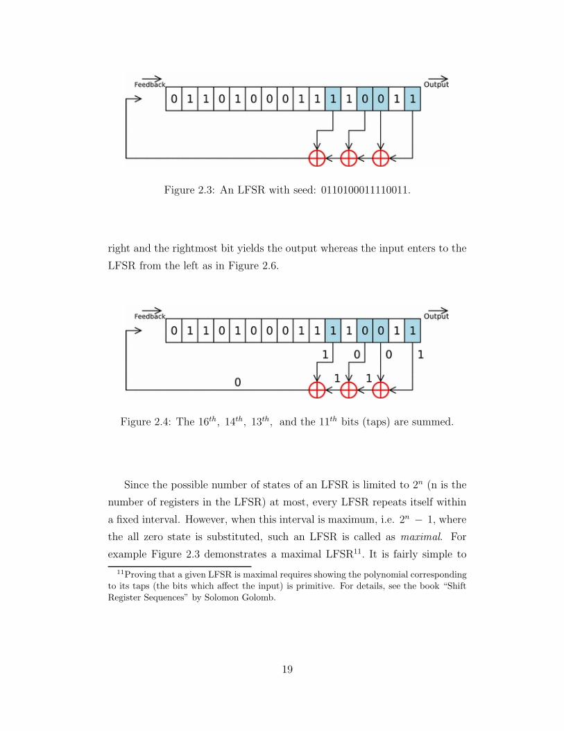
Figure 2.3: An LFSR with seed: 0110100011110011.
right and the rightmost bit yields the output whereas the input enters to the
LFSR from the left as in Figure 2.6.
Figure 2.4: The 16th, 14th, 13th, and the 11th bits (taps) are summed.
Since the possible number of states of an LFSR is limited to 2n (n is the
number of registers in the LFSR) at most, every LFSR repeats itself within
a fixed interval. However, when this interval is maximum, i.e. 2n − 1, where
the all zero state is substituted, such an LFSR is called as maximal. For
example Figure 2.3 demonstrates a maximal LFSR11. It is fairly simple to
11Proving that a given LFSR is maximal requires showing the polynomial correspondingto its taps (the bits which affect the input) is primitive. For details, see the book “ShiftRegister Sequences” by Solomon Golomb.
19

Figure 2.5: The input bit is found as 0.
Figure 2.6: Right shift operation is carried out. Output bit is 1.
implement the LFSR structure on FPGA. The following code segment shows
the implemented LFSR in VHDL:
. . . (Signal declarations follow:)
signal lfsr input : std logic;
signal generator reg : std logic vector(31 downto 0);
. . . (LFSR input is updated using the desired taps:)
lfsr input <= generator reg(0) xor generator reg(10) xor
generator reg(30) xor generator reg(31);
. . . (At the next rising-edge of the clock, LFSR is right-shifted:)
elsif(rising edge(clock)) then
20

generator reg <= lfsr input & generator reg(0 to 30);
. . . (Remaining part of the code follows)
As seen in the example code segment, we used a 32-bit LFSR, which is
maximal. Hence, we generated a pseudonoise (PN) sequence that repeats
itself after 232 − 1 cycles. Our data rate was 1 Mbps, which corresponds to
a repetition interval of approximately 4000 seconds. This figure was enough
to observe a PSD that is quite similar to the PSD of rectangular pulse shaped
BPSK.
2.4.2 Pulse Shaping
During the implementation of the pulse shaping filter for the transmitter, we
considered two main points:
� No intersymbol interference (ISI) at the sampling instants:
For a pulse shape x(t), k being any sampling instance, the no ISI con-
dition can be defined as
x(t = kT ) =
{1 if k = 0
0 if k �= 0. (2.1)
According to the Nyquist pulse-shaping criterion [3], the necessary and
sufficient condition for X(f) is given as
∞∑m=−∞
X(f + m/T ) = T (2.2)
� Bandlimited frequency response: In wireless communications, lim-
iting the bandwidth of a baseband signal is crucial to avoid aliasing
during the IF up-conversion and to suppress out-of-band radiation.
However, a signal limited in frequency domain is unlimited in time do-
main. For that reason, the signal to be implemented should be nearly
limited in frequency for realization of a nearly unlimited time domain
representation.
21

There are many pulse shapes satisfying the first condition noted above. These
pulse shapes constitute a class called Nyquist-I pulse. The smallest band-
width for these pulses is satisfied by the sinc function:
x(t) =sin(πt/T )
πt/T, (2.3)
where T is the symbol duration. In contrast to its bandwidth advantage,
sinc function has a slow decay rate and sensitive to timing phase errors. As a
result, it is usually very hard to approximate the sinc function in time domain
and in case of timing errors, the ISI term in the received signal may increase
indefinitely. For these two reasons, we decided to use another well-known
signal for pulse shaping the symbols to be sent. This pulse shape is known
as raised cosine (RC) and it is usually defined using a parameter named as
the roll-off factor, β. The normalized frequency domain representation for
RC is given by
X(f) =
⎧⎪⎪⎨⎪⎪⎩
1 | f |≤ 1−β2T
12
[1 + cos
(πTβ
[| f | −1−β2T
])]1−β2T
<| f |≤ 1+β2T
0 | f |> 1+β2T
. (2.4)
Since the representation in Eqn. 2.4 is limited in frequency domain, the
corresponding time domain pulse is also unlimited just as in the case of sinc
pulse. Nonetheless, RC pulse shape decay rate is proportional to (1/t3) for
β > 0 case12, whereas sinc function only decays with a (1/t) rate. In this
sense RC pulse shape can be approximated more easily and it has higher
immunity to timing phase errors. The bandwidth occupied by RC filter is
BWRRC =1
2T(1 + β). (2.5)
In our application, since the receiver had to match the transmitter pulse
shaping filter and the overall response had to represent an RC filter, we used
the root raised cosine (RRC) filtering at both ends. The frequency response
12For β = 0 RC pulse shape becomes nothing but the sinc pulse shape.
22

of the RRC filter is just the square-root of the RC response given in Eqn. 2.4.
Our design choice for the roll-off factor was 0.35 due to the effective sampling
frequency at the receiver side (see Section 2.5.3).
During the implementation of pulse shaping (which applied on the pseudo-
random output of the LFSR in Section 2.4.1), we initially generated the de-
sired impulse response of the RRC filter in MATLAB. Then, the filter taps
are normalized and quantized in 6-bit 2’s complement signed format. The
exact RRC pulse shape together with the digital approximate (that is stored
in read-only memory modules of FPGA) is shown in Figure 2.7. The exact
pulse is scaled such that the peak value in the middle is equal to the largest
positive integer (in our case, for 6-bit signed representation, it is 31) for
better visualization of the approximation errors. Moreover, due to 24 MHz
sampling rate of digital-to-analog converter (DAC), and selected 1 Mbps data
rate, the oversampling rate for the RRC filter would be an integer between
1 and 24. Figure 2.7 is drawn with the assumption that approximate filter’s
oversampling rate is 6 and a given sample is constant for 4 time steps in
24 MHz sampled domain. Having a higher oversampling rate means storing
more intermediate samples from exact waveform and better approximation
of RRC pulse. Finally, we divided a symbol time into six intervals, which cor-
responds to oversampling rate of 6. In each interval a distinct value sampled
from the quantized exact waveform is used for realizing the convolution op-
eration with the RRC pulse shape. With 6-bit representation the quantized
values for RRC become zero outside the ±3 symbol interval and 19 sym-
bols (6 for each 3 symbol intervals and a single midpoint) are stored making
use of the symmetry of the RRC pulse shape around its peak (midpoint)
value. The convolution operation is, then, summation of 7 of these samples
or their negated versions according to the values of the symbols to be sent,
when oversampling is taken into account. In our case, for QPSK modulated
symbols, we directly add the sample for a 1 to be sent and add the negated
sample for a 0 to be sent in both in-phase and quadrature-phase branches.
23

−100 −80 −60 −40 −20 0 20 40 60 80 100−10
−5
0
5
10
15
20
25
30
35Ideal RRC Impulse Response in Comparision with Digital 6−bit Approximation
n, discrete time
Qua
ntiz
atio
n L
evel
Exact RRC Impulse ResponseDigitial Approximation
Figure 2.7: Digital RRC filter closely approximates the exact waveform
within ±3 symbol interval.
The RRC pulse shape (and its approximation) is not causal as seen in
Figure 2.7. This results in the requirement that at least 3 past symbols sent
should also be kept for adding their pulses’ tails to the current symbols pulse
shape. We solved this issue simply by taking the 29th bit of the LFSR as
the current bit to be transmitted and taking the 30th, 31st, and 32nd bits as
the past bits. In accordance with that idea, the 28th, 27th, and 26th ones are
the next bits effecting the current bit. Applying this filter on the random
sequence of BPSK symbols, we obtained the time and frequency domain
signals as in Figures 2.8 and 2.9. The quantization levels (steps) for the
time domain representation are obvious. If we take the PSD of the filter
output into consideration, the first thing to note is that occupied bandwidth
is very close to 0.675 MHz, which is also the expected bandwidth found from
24

515 520 525 530 535 540
−40
−30
−20
−10
0
10
20
30
40
Output Signal of Digital RRC Filter with BPSK Input
t, μsec
Qua
ntiz
ed O
utpu
t
Figure 2.8: Digital RRC Filter Output
−10 −5 0 5 10−60
−50
−40
−30
−20
−10
0PSD of Digital RRC Filtered BPSK Sequence
f, MHz
Nor
mal
ized
Pow
er p
er H
z
Figure 2.9: The PSD of the digital RRC filter output.
25

Eqn. 2.5 with β = 0.35. Secondly, there are harmonic signals at f=6 MHz and
f=12 MHz distorted by a sinc type multiplicative signal. The signal around
f=6 MHz is approximately 25 dB weaker than the baseband signal; therefore
was observed to have limited effect during the IF conversion described in
Section 2.4.3. A lowpass filter placed before the I/Q modulation stage may
improve the performance further.
2.4.3 I/Q Modulation
QPSK modulation is performed to transmit data after RRC pulse shaping
for BPSK modulated data. In order to generate two bit streams, we used two
LFSRs with different seeds. We quantized single period of a 3 MHz sine signal
in MATLAB and formed an 8-bit resolution sine lookup table (with 8 entries)
from this quantized data in VHDL. We synthesized a free-running counter for
accessing this table to form a digital sine signal and used quarter-length (90◦)
shifted version of that counter to form the cosine signal. After multiplying
the in-phase and quadrature-phase RRC shaped signals with cosine and sine
signals, the difference of the products were ready to be given to DAC board.
Figure 2.10 demonstrates the PSD for the IF QPSK signal taken as input by
the DAC. Obviously, the baseband RRC type frequency response is carried
to the IF, which is 3 MHz in our implementation. The effect of the harmonic
signal that was present before the conversion is negligible. The IF signal
given to the DAC is converted into analog form and transmitted after an RF
up-conversion.
2.5 Receiver Structure
The receiver side, in fact, carries out similar operations to the transmit-
ter, however in the reverse order. Mainly, initial steps constitute RF to
IF down-conversion, sampling of the IF signal, I/Q demodulation, and low-
pass filtering to obtain the baseband equivalent signal. Following these steps,
26

−10 −5 0 5 10−60
−50
−40
−30
−20
−10
0PSD of Upconverted (IF) QPSK Sequence
f, MHz
Nor
mal
ized
Pow
er p
er H
z
Figure 2.10: The PSD of the digital I/Q modulation output.
RRC matched filtering is applied and finally, the symbols are detected. Other
than these steps, some auxiliary steps should also be implemented. Firstly,
the start for the group of bits, which is called a packet, must be detected.
The optimal detection points for bits needs to be found and effects of the
channel and the frequency offsets should be estimated. It is common to most
telecommunications systems that the receiver structure is much more sophis-
ticated than the transmitter. In accordance with this trend, our receiver
setup (with all the blocks stated above) is also almost six times more com-
plicated than the transmitter in terms of the logic area usage on the FPGA
chip. Figure 2.11 demonstrates the complexity of the receiver side better.
Now, we will explain in detail the receiver blocks one by one in the order
of their operation on the received data.
27

Figure 2.11: Reception, processing and detection tasks carried out in the
receiver side are summarized.
28

2.5.1 Serial to Parallel (LVDS to CMOS) Conversion
We described in Section 2.2.3 that the 12-bit samples of the analog data are
given in serial LVDS pairs together with data and frame clocks by the ADC
board. After being conveyed to the FPGA board through an interface board,
this serial data bits needs to be converted into 12-bit parallel data. This posed
one of the biggest problems we faced, since not only the serial to parallel
(S/P) conversion requires adequate usage of two different frequency clock
signals, but also it has to be done by a circuit with a very low combinational
delay. We aimed to design the simplest possible S/P converter that can
sample the received serial bits at the rising- and the falling-edges of the data
clock. Although the serial LVDS data rate in our case (6×24 = 144 MHz) was
moderate when compared with the upper limit of the ADC (nearly 400 MHz),
the design was still demanding. The initial phase was to convert the obtained
LVDS pair into a single ended CMOS signal that can be used by our design.
The LVDS buffers and the LVDS clock buffers located on some special parts
of the FPGA were the solution for voltage level conversion. Following this,
we separated the S/P conversion block from the other design units and put
some timing constraints so that all the S/P conversion related logic should
satisfy 144 MHz operating frequency. These precautions made Xilinx ISE
synthesize and implement a logic that meets our timing requirements. To
obtain the first results, the parallelized data is tested by setting the ADC
to transmit some factory-coded test patterns without actually sampling the
received signals. Then, a logic block for converting the binary offset (see
Section 2.2.3) representation into 2’s complement had been written. Finally,
assuring the correct operation of the S/P converter we used this structure
until the realization of multiple receiver antenna system. The multi-antenna
system is more complicated with timing constraints becoming harder to meet.
Therefore, an improved version of this S/P converter is given in Section 2.6.2.
29

2.5.2 I/Q Demodulation
The sine lookup table discussed in Section 2.4.3 is used for I/Q demodulation
with a slight difference in content and operation. We added some intermedi-
ate values to sine samples in order to increase time domain resolution of the
representation. The overall table had 256 8-bit samples from a single period
of a sine function. This method has barely any effect on the performance
when sine lookup table is directly accessed with 32-step increments13 in the
counter that is used for accessing the table. However, a feedback signal com-
ing from the frequency synchronization block (see Section 2.5.8) orders the
local oscillator signals to shift the frequency of the sine and cosine signals
in small amounts for frequency offset mitigation. Hence, having a sine table
with higher resolution in time allows this frequency correction operation to
be more precise.
The I/Q demodulation operation involves multiplication of the received
signal samples with the digitally generated sine and cosine signals. From
this point on, we have two branches on which we will apply the identical
filtering operations. (Hereafter one of these branches will be referenced as
I for in-phase component of the received signal and the other one as Q for
quadrature-phase component.) Since multiplication with a sinusoidal sig-
nal creates images of the desired baseband signal at twice the modulation
frequency, both I and Q branches seem distorted at the output of the I/Q
demodulator in Figure 2.12. In addition to the effect of high frequency sig-
nals, the power levels of I and Q branches are different. This is mainly due to
the channel response multiplying the baseband equivalent complex (QPSK)
signal. Such a multiplication modifies both the magnitude and the phase of a
QPSK signal. With phase distortion, if the transmitted signal is (1 + j) and
the phase of the channel response is 45◦, the corresponding I/Q demodulator
output will be on the imaginary axis with zero power in the I branch. Since
1332-step increments in a 256-entry sine lookup table with a clock frequency of 24 MHzcorresponds to generating 3 MHz sinusoidal signals just as in the transmitter side.
30

0 200 400 600 800 1000 1200−0.5
0
0.5
n, discrete time
Nor
mal
ized
Vol
tage
I/Q Demodulation Output: In−phase Component
0 200 400 600 800 1000 1200−0.5
0
0.5
n, discrete time
Nor
mal
ized
Vol
tage
I/Q Demodulation Output: Quadrature−phase Component
1 1 1 1
0 0 0
Figure 2.12: I and Q branch outputs after I/Q demodulation.
the phase correction to remedy this problem is given in Section 2.5.6, we will
point out a final detail in Figure 2.12. In spite of the deteriorations at the
output of the I/Q demodulator due to noise, the 7-bit Barker code sequence14
is still observable with RRC pulse shaping at the Q branch output as shown
by arrows.
2.5.3 Integrate and Dump Filtering
Having two identical implementations of this filter for handling I and Q
branches simultaneously, we had the following reasonings for having them in
the system:
� After demodulating the received signal, I and Q branches have high
frequency terms as well as the desired baseband terms. A low pass
147-bit Barker sequence is 1,1,1,0,0,1,0.
31

filtering is desired to cancel these high frequency terms out.
� Since the signal is sampled at 24 MHz, we have 24 samples for each bit
to be decoded. Even if we take the excess bandwidth (resulting from the
usage of RRC filter with non-zero β value) into account, the sampling
rate is still much higher than the Nyquist frequency. The finite impulse
response (FIR) RRC matched filter should have (6 × 24 + 1 = 145)
taps, which is very costly to implement.
The integrate and dump filters (IDFs) accumulate15 their discrete inputs by
summing them up for a defined interval and at the end of this interval gives a
single output for all the summed up signals. Hence, being an averaging filter
it behaves as a lowpass filter eliminating the high frequency terms. Moreover,
it decreases the number of samples per bit at its output by down-sampling the
input data. Our IDF realization sums 8 consecutive samples16 and outputs
the average of them before accumulating next 8 samples. Following the
IDF, the sampling frequency is decreased by 8 and becomes 3 MHz, which
diminishes the logic area that the next stage filters consume. The effect of
the IDF filter can be better understood by observing the Figures 2.13, 2.14,
and 2.15. In Figure 2.13, the effect of eliminating the high frequency terms
at the output of the I/Q demodulator is noted as having smoother curve
in comparison with the results in Figure 2.12. Figure 2.14 proves us the
existence of high frequency term at 6 MHz having a comparable power with
the desired baseband signal for the I branch. Moving to the Figure 2.15, we
can easily discriminate the desired RRC shaped baseband frequency response
at the output of the IDF for the I branch.
15Correspond to integrating in continuous time.
16In fact, the frequency response of an IDF is sinc type (not a lowpass type) and thefirst null is at 6 MHz for this case.
32

0 50 100 150−0.5
0
0.5
n, discrete time
Nor
mal
ized
Vol
tage
Integrate and Dump Filter Output: In−phase Component
0 50 100 150−0.5
0
0.5
n, discrete time
Nor
mal
ized
Vol
tage
Integrate and Dump Filter Output: Quadrature−phase Component
Figure 2.13: I and Q branch outputs after IDF.
−10 −5 0 5 10−60
−50
−40
−30
−20
−10
0PSD of I/Q Modulated Output Before IDF: In−phase Component
f, MHz
Nor
mal
ized
Pow
er p
er H
z
Figure 2.14: PSD of I branch includes high frequency term at 6 MHz.
33

−1.5 −1 −0.5 0 0.5 1 1.5−60
−50
−40
−30
−20
−10
0PSD of IDF Output: In−phase Component
f, MHz
Nor
mal
ized
Pow
er p
er H
z
Figure 2.15: RRC frequency response with BW=0.675 MHz is clearly ob-
served.
2.5.4 Matched Filtering
The matched filter is exactly the same pulse shaping filter used as the trans-
mitter side, however since the sampling frequency at the output of the IDF is
3 MHz, an RRC filter with oversampling rate of 6 can not be realized for the
receiver. Therefore, the oversampling rate for the matched filter is 3, which
corresponds to building up an FIR filter with 19 taps under the assumption
that only the symbols at a distance less than or equal to 3 are effective on
the current symbol. A filter with 19 taps requires 19 multiplications and
18 additions for evaluation of an output at each instance. In order to avoid
slowing down of this operation, we used two approaches while coding the
matched filter:
� Multiplication operation is usually more time-consuming than simple
shifting operations and there are only limited number of fast multipli-
34

ers on our board as stated in Section 2.2.1. Therefore, we preferred
arithmetically shifting the inputs to the left to multiplying them with
tap weights. For example, multiplication by 5 is implemented as adding
the input value to its 2 times arithmetically left-shifted version.
� Although we removed away the multipliers from our RRC design, still
we had many additions, even more than what we would have had when
we used multiplication. If all of the additions were to be carried out in
single clock time, this would result in a very high combinational delay
that the RRC filter would be useless. At this point, the pipelining was
thought to be the key for decreasing combinational delay of the matched
filter. With pipelining it is possible to evaluate the results of subsets
of all the additions separately and joining these intermediate results to
evaluate the final result by either using another pipelining stage(s) or
directly adding them up. As expected, pipelining comes with its own
cost, excessive storage area used by the intermediate results in different
pipelining stages. In contrast to the excessive multiplier usage and high
combinational delay issues, this problem is fairly acceptable especially
when a good pipelining design taking care of the structure of the filter
is done. After designing the matched filter, we plotted the experimental
data taken from FPGA in MATLAB, which is given in Figure 2.16.
2.5.5 Packet Synchronization and
Correlation Filtering
For detecting the existence and determining the beginning of data packets
we add a pilot symbol sequence at the start of each packet. Although various
kinds of pilot symbols may be used for this purpose, we mainly concentrated
on a specific class of sequences that are also utilized in practice [5]. We ap-
pended 7-bit and 13-bit Barker codes as the prefix of transmitted packets
of length 512 or 1024 bits. The Barker codes are known for their low auto-
correlation sidelobe properties. The 7-bit packet prefix is (1,1,1,0,0,1,0) and
35
100 110 120 130 140 150 160−0.5
0
0.5RRC Matched Filter Output: In−phase Component
t, μsec
Nor
mal
ized
Vol
tage
100 110 120 130 140 150 160−0.5
0
0.5RRC Matched Filter Output: Quadrature−phase Component
t, μsec
Nor
mal
ized
Vol
tage
Figure 2.16: Power in I and Q branches are quite close to each other, which
indicates that instantaneous phase of channel response is close to a multiple
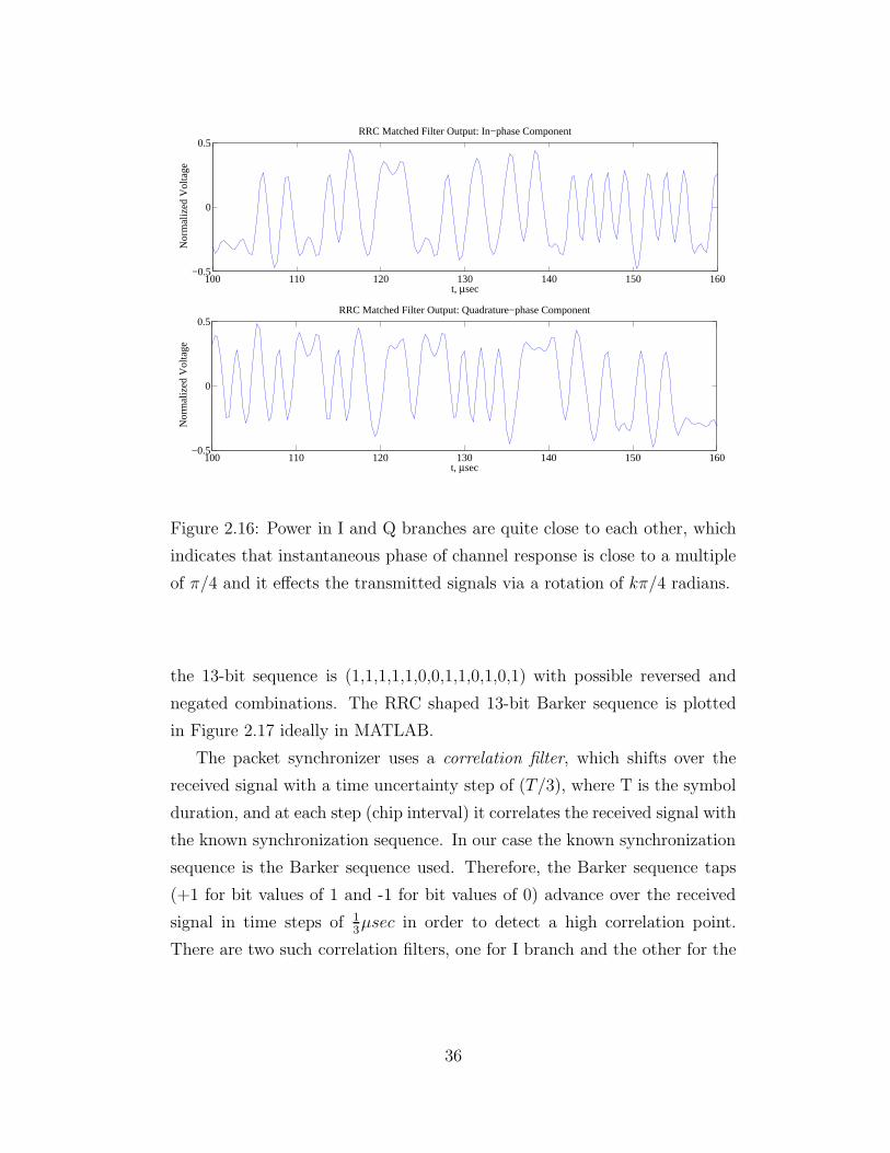
of π/4 and it effects the transmitted signals via a rotation of kπ/4 radians.
the 13-bit sequence is (1,1,1,1,1,0,0,1,1,0,1,0,1) with possible reversed and
negated combinations. The RRC shaped 13-bit Barker sequence is plotted
in Figure 2.17 ideally in MATLAB.
The packet synchronizer uses a correlation filter, which shifts over the
received signal with a time uncertainty step of (T/3), where T is the symbol
duration, and at each step (chip interval) it correlates the received signal with
the known synchronization sequence. In our case the known synchronization
sequence is the Barker sequence used. Therefore, the Barker sequence taps
(+1 for bit values of 1 and -1 for bit values of 0) advance over the received
signal in time steps of 13μsec in order to detect a high correlation point.
There are two such correlation filters, one for I branch and the other for the
36

0 10 20 30 40 50 60−50
−40
−30
−20
−10
0
10
20
30
40
50RRC Shaped Ideal Barker Sequence
n, discrete
Qua
ntiz
atio
n L
evel
Figure 2.17: MATLAB plot of the 13-bit Barker code.
Q branch. The ideal method for detecting a new packet requires the joint de-
tection over two branches. Since we transmit the same Barker sequence over
two branches, the packet synchronization module simply finds the squares of
the correlation filters and sums these results17, which is given as,
btotal [n] = b2I [n] + b2
Q [n] . (2.6)
In Eqn. 2.6, bI [n] and bQ [n] denote the outputs of the correlation filters of
the I and the Q branches respectively. Figure 2.18 gives an idea about the
measure (btotal [n]) that is used for determining the start of a new packet.
In Figure 2.18, the first normalized peak value is found to be 0.4594, while
the sidelobe value with datatip is 0.00421. Hence, the ratio of the peak-
17This method is ideal for the case that noise in the received signal is complex AWGN.
37

0 20 40 60 80 100 120 140 1600
0.05
0.1
0.15
0.2
0.25
0.3
0.35
0.4
0.45
0.5
X: 7.667Y: 0.00421
FPGA Packet Synchronization Module Output, btotal
[n], for Only Barker Sequence (13−bit) Transmission
t, μsec
Nor
mal
ized
Pow
er
X: 15.67Y: 0.4594
Figure 2.18: Peak points showing the start of data packets and the small
sidelobes are clearly distinguishable.
to-sidelobe is nearly 109, which is a bit smaller than the ideal ratio18 for
btotal [n] with no noise in the channel. In addition to this, the peak values for
consecutive Barker sequences slightly differ from each other. As a result, it
is usually impractical to set a constant limit for detection of the packet start
peaks. On the contrary, the threshold in our system is calculated according
to two parameters: the expected value of the noise power and the estimated
signal power. The expectation for noise power is obtained by lowpass filtering
the correlation power output, btotal [n], of the packet synchronization module.
This lowpass filter is an infinite impulse response (IIR) filter whose update
18Ideal peak-to-sidelobe ratio is the square of bits used in the sequence, hence 169 forthis example.
38
equation is given as,
mnoise [n] =
{k−1
kmnoise [n − 1] + 1
kbtotal [n − 1] if not in a packet
mnoise [n − 1] if in a packet. (2.7)
According to Eqn. 2.7, the expectation of the noise signal power is updated
(calculated) only if the system is waiting for a packet arrival. If a packet
is already being sampled or the leading sidelobes of the correlation power
output has arrived, due to possibly very high signal power, the noise power
update is paused until the end of the current packet19. Another important
topic is the selection of the k value in the update equation. With smaller
values of k, the filter tend to approximate the noise power using less number
of past values. However, very large values also has a disadvantage, since
the input (btotal [n − 1]) to the filter is divided by larger numbers which may
result in loss of data in the least significant bits or even the input may be
totally nulled. After some trial and error, we decided to use k = 64.
The signal power estimation is based on the detection of the levels of the
leading sidelobes of the correlation power output. The higher the sidelobes,
the higher should be the threshold that btotal [n] surpass. Moreover, any point
should be a peak (maximum point) in order to be classified as a starting
instance for a packet. This is handled by storing the past value and also
a future value of btotal [n] so that any point over the threshold can also be
compared with its neighboring points. (As an example, in Figure 2.18, the
point marked with the datatip around t = 16 μsec is larger than the points
on its left and right, hence is a maximum point.) Then, a maximum point
higher than the adaptively determined threshold value marks the start of a
new packet, which triggers the channel response estimation and bit sampling
procedures.
19Our transmitter structure guarantees that there will be empty periods between packetsso that no data will be transmitted in these periods.
39

2.5.6 Channel Response Estimation and Phase Cor-
rection
In most practical systems it is crucial for the receiver to estimate the effects
of the medium that the received data is transmitted in. This estimation is
commonly known as channel response estimation. In our receiver structure,
if we denote the received signal as y [n], the channel response as h [n], and
the noise sample as w [n] at the instant n, the relation between transmitted
symbol, x [n], and y [n] can be written as,
y [n] = h [n] x [n] + w [n] . (2.8)
In Eqn. 2.8, the most important assumption is that channel response can be
approximated by a single constant complex number. Therefore, the channel
is assumed to be frequency non-selective (flat-fading or ISI-free). Moreover, if
we assume that the channel response, h [n], is constant also within the packet
length (which is acceptable for packet duration of 512 μsec in most indoor
mobility cases), then estimating the value of h [n] at the start of a packet
(hence dropping the discrete time index), channel equalization is performed
by,
y [n] =h�y [n] (2.9)
= | h |2 x [n] + h�w [n] . (2.10)
The operation in Eqn. 2.9 involves complex multiplication of the received
complex signal with another complex number’s conjugate. On FPGA, this
can be realized as in the following code segment,
. . . (Signal declarations and other parts that precede are removed.)
if( (corr power 1past >= threshold) and
(corr power 1past >= corr power) and
(corr power 1past >= corr power 2past)) then
ch resp I <= barker corr I;
40

ch resp Q <= barker corr Q;
. . . (The codes in between are removed.)
I corrected <= (rrc I − rrc Q) * ch resp I +
(rrc I + rrc Q) * ch resp Q;
Q corrected <= (rrc I + rrc Q) * ch resp I −(rrc I − rrc Q) * ch resp Q;
. . . (Remaining part of the code follows.)
The initial if statement in the code searches for the packet synchroniza-
tion point as described in Section 2.5.5. However, channel response value
obtained in this code uses directly the correlation filters’ outputs at the
packet initialization instance. In fact, since the transmitter side sends the
same Barker sequence from both I and Q branches, the found channel re-
sponse corresponds to the effect of channel on complex symbol x [n] = 1 + j
instead of simply x [n] = 1. Therefore, we have to divide the found h [n]
value by (1 + j) in order to carry out the operation described in Eqn. 2.9.
The remaining parts of the above code segment takes care of this issue to
obtain the corrected20 I and Q values for x [n]. For QPSK (and BPSK) mod-
ulation only the received signal’s phase is important. There is no need for
correcting the magnitude of the symbols to be detected unless non-constant
amplitude modulation techniques are used. Therefore, the (| h |2 x [n]) term
in Eqn. 2.10 was left as it is before detecting the QPSK symbols.
Obtaining the channel response values for consecutive packets, we plot
these complex numbers in the complex domain to observe their characteris-
tics. The scatterplot for the estimated experimental h [n] values (channel is
the transmission medium, that is air, for all of the experiments) are given in
Figure 2.19. The Figure 2.19 is drawn by estimating 32 consecutive channel
response values at five different time intervals, while the transmitter and the
20The correction at this point is only for the channel phase subtraction, no magnitudecorrection is carried out.
41

−0.02 −0.01 0 0.01 0.02
−0.025
−0.02
−0.015
−0.01
−0.005
0
0.005
0.01
0.015
0.02
0.025
Imag
inar
y Pa
rt o
f C
hann
el R
espo
nse
Real Part of Channel Response
Channel Response Estimations on Complex Domain
RotationDirection
Figure 2.19: The phase of the channel response varies fast.
receiver antennas are in line of sight (LOS). Each one of these five groups
span 1 msec intervals. Surprisingly, although the magnitude of the estimates
stays nearly constant, the phase varies in a relatively fast pace so that the
channel response rotates almost by π6
radians within 1 msec. This would
mean that for symbol time of 1 μsec and packet length of 1500 bits, a symbol
value of (1+j) becomes√
2 (with no imaginary component at all) at the end
of the packet, which will result in false detections even if no noise is present
in the received signal. Hence, it is almost impossible to transmit packets
longer than 1000 bits by estimating the channel response only at the start
of the packet or without finding the reason for the rotation in the channel
response. The solution for avoiding this rotation is given in Section 2.5.8.
42
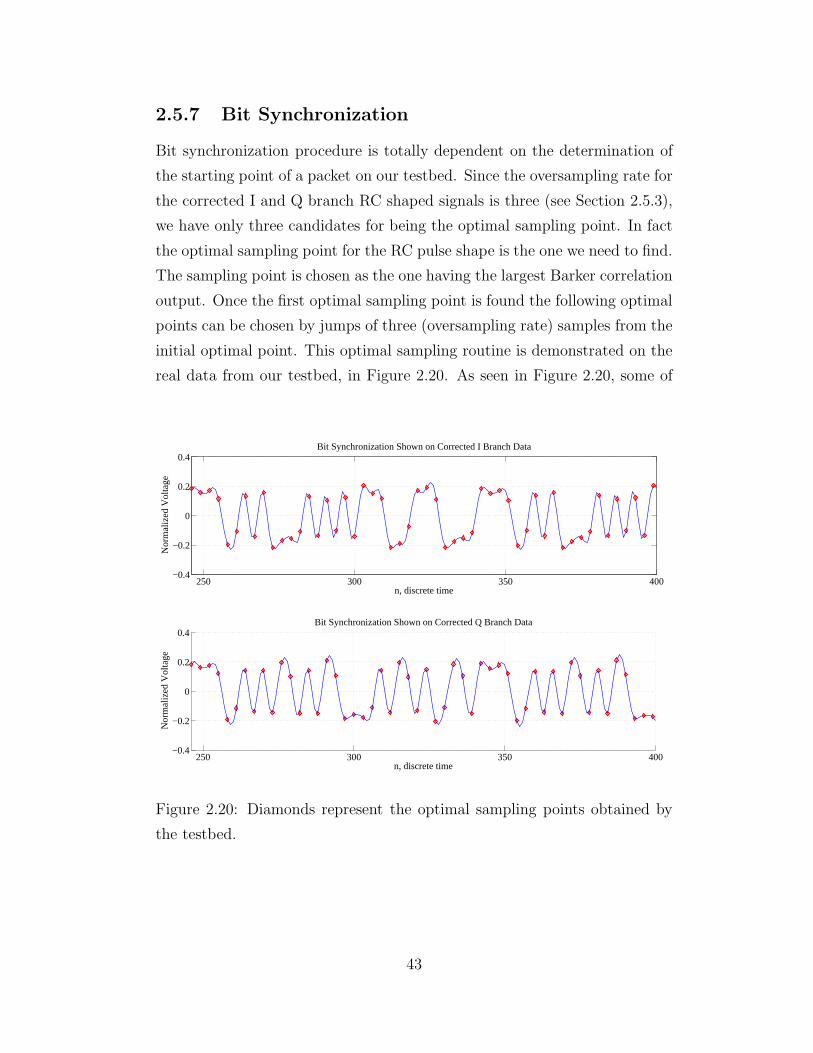
2.5.7 Bit Synchronization
Bit synchronization procedure is totally dependent on the determination of
the starting point of a packet on our testbed. Since the oversampling rate for
the corrected I and Q branch RC shaped signals is three (see Section 2.5.3),
we have only three candidates for being the optimal sampling point. In fact
the optimal sampling point for the RC pulse shape is the one we need to find.
The sampling point is chosen as the one having the largest Barker correlation
output. Once the first optimal sampling point is found the following optimal
points can be chosen by jumps of three (oversampling rate) samples from the
initial optimal point. This optimal sampling routine is demonstrated on the
real data from our testbed, in Figure 2.20. As seen in Figure 2.20, some of
250 300 350 400−0.4
−0.2
0
0.2
0.4
n, discrete time
Nor
mal
ized
Vol
tage
Bit Synchronization Shown on Corrected I Branch Data
250 300 350 400−0.4
−0.2
0
0.2
0.4
n, discrete time
Nor
mal
ized
Vol
tage
Bit Synchronization Shown on Corrected Q Branch Data
Figure 2.20: Diamonds represent the optimal sampling points obtained by
the testbed.
43

the sampling points coincide with the optimal RC sampling points very well,
whereas some others (like the 6th sample of Q branch) do not. This is mainly
due to two reasons:
� Since the oversampling rate is only three, there is still a high chance
that all the three points misses the optimal point.
� The rotation of the channel response described in Section 2.5.6 results
in phase offsets dynamically changing the real sampling points through-
out the packet, while our receiver decides on the optimal points for
whole packet once only at the beginning of it.
The solution to the first reason has a high cost associated with it, since
increasing the sampling rate would require all the filters, following the IDF,
to have more input signals to be processed at an instant. (See Section 2.5.3
for details.) Therefore, we mainly concentrated on the second reason for
non-optimal sampling in Section 2.5.8.
2.5.8 Frequency Synchronization and Bit Detection
When we analyzed the reasons for channel response rotation described in
Section 2.5.6, we observed that the rotation direction of the channel re-
sponse changes from clockwise to counterclockwise when we exchange the
crystal oscillators used at the receiver and the transmitter sides. After that,
we carefully investigated the frequency offset between these two roughly 24
MHz oscillators to find a frequency difference of nearly 640 Hz. This offset
corresponds to a (640/8 = 80 Hz) difference at 3 MHz, which is the carrier
frequency for our IF signals. If we model that IF offset as a modulating
sinusoidal signal with period ((80 Hz)−1=12.5) msec, this would result in a
channel rotation of (2π (1 msec)(12.5 msec)
) = ( 2π12.5
) in 1 msec that is very close to the
rotation observed in Figure 2.19.
The larger frequency offsets between the IF frequencies generated on two
sides of our testbed result in faster rotations of the channel response esti-
44

mates. As a result, the expected value of the rotation angles between con-
secutive channel response estimates gives a metric for frequency mismatch.
Therefore, we desire a mechanism for calculating the phase of the channel
response estimates and for averaging the phase differences over many esti-
mation results.
Coordinate rotation digital computer (CORDIC) [6] is an algorithm espe-
cially used for calculating trigonometric, hyperbolic, logarithmic functions, or
division and square root operations, where no or limited multiplication units
exist. A CORDIC-based algorithm makes use of only additions, arithmetic
shift operations, and a fairly small size lookup table. It tries to converge
to the correct result by successive approximation iterations. The resolu-
tion of the final result (so the number of iterations to be made) depends
on the size and the resolution of the lookup table utilized. In our case, we
used a CORDIC-based algorithm to calculate the phase of each channel re-
sponse estimate. The lookup table, for this implementation, is filled with
digital representations of various arctangent values. There are eigth 8-bit
representations: acrtan(1), arctan(1/2), . . . , arctan(1/128). In the first step
algorithm starts with assuming the phase to be calculated is 0, π, or −π
radians according to the quadrant of the channel response and modifies the
channel response. In the second step it adds/subtracts arctan(1) = π/4,
the first lookup table entry, from the initial guess by observing the sign of
the modified channel response and modifies the channel response once more.
Continuing in this fashion the algorithm adds/subtracts smaller and smaller
angles at each step and obtains a result with an error on the order of the
last lookup table entry after the 8th step. If we convert the last entry of the
lookup table into degrees, the maximum error in phase calculation is only
0.45◦ with 8 iterations that would be done in 8 μsec after start of the packet
is detected.
Final point in frequency synchronization is obtaining an expected (aver-
age) value for frequency offset. This is accomplished by using a simple IIR
filter that bare resemblance to the IIR filter in Eqn. 2.7, but with k = 8.
45

This filter operates only once for each packet. The output of this filter gives
us information about the sign and the magnitude of the frequency differ-
ence between the transmitter and receiver. These two parameters modify
the frequency of the generated IF demodulation signals. As explained in
Section 2.5.2, the sine and the cosine signals are generated using a 256-entry
table, which includes the samples from a period of a sine function. If no fre-
quency difference is present between sides, this table is accessed by 32-step
increments at each clock cycle to synthesize 3 MHz signals. Whenever the
frequency offset results in an output signal of non-zero magnitude for the
IIR filter of frequency synchronization module, this 32-entry step is altered
to 31- or 33-entry steps in order to accelerate/decelerate the receiver sides
signals. A 31-entry jump is used for accelerating the sine and cosine signals,
whereas a 33-entry jump slows down these signals. Since these short/long
(abnormal) steps are used only once in hundreds (or even thousands) of nor-
mal steps, the resulting sine and cosine signals do not deteriorate much, but
they are only slightly frequency shifted. The counter which determines the
period of abnormal steps is adaptively updated according to the newly ob-
tained phase differences from consecutive channel response estimates, which
completes the feedback loop. To manifest the tremendous effect of frequency
synchronization block on the recorded experimental channel response esti-
mates, we implemented a test scenario, in which 1024 packets each with 512
QPSK symbols are transmitted. The channel response estimates without
and with the digital phase-locked loop-like (D-PLL-like) structure are given
in Figure 2.21. It is obvious that the channel response do not change much
between consecutive packets, according to Figure 2.21. The channel response
rotates over itself completing many tours when the frequency synchroniza-
tion unit is non-operational (left-hand side). However,when it is operated,
the rotation for 1024 packets is almost 42◦, which gives an average rotation
of 0.041◦ between two consecutive packets. Let us, finally, demonstrate the
effect of frequency synchronization, this time, for the QPSK symbols to be
detected. The presented data on Figure 2.22 is experimental data, which is
46

acquired from the digital bit detector on FPGA, using the serial port commu-
nication. In Figure 2.22, QPSK symbol constellation diagram is plotted for
the case when the frequency synchronization block on FPGA is deactivated
(shown on the left-hand side) and the case when it is activated (shown on
the right-hand side). Both of the experiments are carried out using single
1024-symbol packet with previously known content and QPSK modulation.
The bit detection is done on I and Q branches separately, since signal levels
on these two branches are independent. For both branches, if the signal is
negative then a 0 is decided; otherwise a 1 is decided. The performance mea-
sure for this single input single output (SISO) system is given in comparison
with single input multiple output (SIMO) system in Section 2.6.3.
−0.1 −0.08 −0.06 −0.04 −0.02 0 0.02 0.04 0.06 0.08 0.1−0.1
−0.08
−0.06
−0.04
−0.02
0
0.02
0.04
0.06
0.08
0.1Channel Response Estimates without Frequency Synchronization
Real Part of Channel Response
Imag
inar
y Pa
rt o
f C
hann
el R
espo
nse
−0.1 −0.08 −0.06 −0.04 −0.02 0 0.02 0.04 0.06 0.08 0.1−0.1
−0.08
−0.06
−0.04
−0.02
0
0.02
0.04
0.06
0.08
0.1Channel Response Estimates with Frequency Synchronization
Real Part of Channel Response
Figure 2.21: The phase of the channel response estimates changes very slowly
in case of frequency synchronization.
47

−0.2 −0.15 −0.1 −0.05 0 0.05 0.1 0.15 0.2−0.2
−0.15
−0.1
−0.05
0
0.05
0.1
0.15
0.2QPSK Constellation Diagram without Frequency Synchronization
Real Part of QPSK Symbols
Imag
inar
y Pa
rt o
f Q
PSK
Sym
bols
−0.2 −0.15 −0.1 −0.05 0 0.05 0.1 0.15 0.2−0.2
−0.15
−0.1
−0.05
0
0.05
0.1
0.15
0.2QPSK Constellation Diagram with Frequency Synchronization
Real Part of QPSK Symbols
Imag
inar
y Pa
rt o
f Q
PSK
Sym
bols
Figure 2.22: Many symbols would be incorrectly detected if no frequency
synchronization were utilized.
2.6 SIMO System Setup
Once all of the blocks of SISO testbed are developed and verified, we set the
goal of operating multiple-antenna cases for receiver, then transmitter, and
finally both sides. In the following sections, there will be information on the
two receiver antenna structure.
2.6.1 Maximal Ratio Combining for
Two Receive Antenna System
One of the frequently faced problems for the wireless systems is fading. The
main reason for fading in wireless systems is the multipath phenomena. Usu-
ally, the transmitter and the receiver are in an environment consisting of
many reflectors and scatterers such that the transmitted signal reaches the
destination following many paths. Each path has its own attenuation and
phase-shifts and the receiver observes a superposition of these signals from
48
multiple paths. At some point in space, these signals may add constructively,
whereas within a small distance, at an other point they may add destruc-
tively. This results in wild variations in the received signal power, hence the
system SNR. When the phases of these signals are assumed to be uniformly
distributed in (0, 2π) and independent from each other, the magnitude of
the superposition result (received signal) is Rayleigh distributed [7], which is
given as,
pZ(z) =z
σ2exp
(− z2
2σ2
), for z ≥ 0, (2.11)
where z is the amplitude of the received signal and σ2 is the variance of
the received signal’s real and imaginary components. The power of received
signal is exponentially distributed and given as,
pX(x) =1
2σ2exp
(− x
2σ2
), for x ≥ 0, (2.12)
where x denotes the power of the received signal. Hence, with moderate
average channel SNR (2σ2) values, there is a good probability that the in-
stantaneous channel SNR is below a threshold level under which the wireless
communication system of interest will be unable to support reliable com-
munication. In such a case, the channel is said to be in deep fade and
communication stops until the received power exceeds the threshold value.
The usual way to fight fading in wireless channels is creating some type
of diversity in one or more of the communication domains: frequency, time,
space, . . . The probability of having all of the diversity elements experience
deep fade at the same time is much smaller than the probability of a single
element facing a deep fade, if the signals for all these diversity elements are
independent. Therefore, with diversity, the reliable communication between
the transmitter and the receiver is supported unless all of the diversity el-
ements fail. We, while building our testbed, used the spatial domain for
obtaining diversity gain and anticipated that if at least one of the spatial di-
versity elements (receiver antennas) could survive, the communication would
not fail due to other elements.
49

In our single input multiple output (SIMO) system, we used two receiver
antennas in order to create spatial diversity. In general, assuming that all the
Mr receiver antennas are placed at such distances from each other that they
observe independent fading, there are many ways of combining the received
signals from different antennas. The combined signal is a weighted sum of
the received signals. In Figure 2.23, s(t) denotes the transmitted signal, h1,
Figure 2.23: Combined output is a linear combination of the received signals.
h2, . . . , hMr denote the complex channel gains for paths from the transmitter
antenna to the receiver antennas, and α1, α2, . . . , αMr the complex weighting
factors that the combiner apply to each of the received signals. In the case
50
that more than one of the signals are weighted by non-zero αi values, these
αi values must be selected in a way that the weighted signals should not add
up destructively under any realizations of hi values. Therefore, the selection
of the phases for non-zero αi’s require,
αi = aie−jφi, (2.13)
where φi is the phase of the ith channel response (hi = riejφi) and ai’s are
real.
The optimal way of combining the diversity branches is named as the
maximal ratio combining (MRC) [8]. With MRC, the ai values are selected
in order to emphasize the signals with higher SNR values and to weight the
signals having lower SNR values with smaller factors. This approach achieves
the maximum SNR for the combined output signal if ai values are chosen as,
a2i = r2
i /Ni, i = 1, 2, . . . , Mr. (2.14)
In Eqn. 2.14, Ni is the noise power in the ith channel and therefore γi = r2i /Ni
represents the SNR for this channel. Then, the maximum total SNR for the
combined output is given as,
γtotal =
(∑Mr
i=1 (aie−jφi)(rie
jφi))2
∑Mr
i=1 | aie−jφi |2 Ni
, (2.15)
=
(∑Mr
i=1 airi
)2
∑Mr
i=1 a2i Ni
. (2.16)
If we place optimal ai values given in Eqn. 2.14, into Eqn. 2.16, and assume
that the Ni values for all channels are the same and equal to N0, the total
51

SNR is given as,
γtotal =
1N0
(∑Mr
i=1 r2i
)2
∑Mr
i=1r2i
N0N0
, (2.17)
=Mr∑i=1
r2i /N0, (2.18)
=
Mr∑i=1
γi. (2.19)
Hence, the maximum total SNR is obtained as the sum of SNR values for
all receiver antennas when we utilize MRC as our combining scenario. For
the two-antenna testbed, simply assuming noise power is identical for two
receiver antennas, we carried out the same operation for combining the re-
ceived signals. Therefore, we detected the QPSK symbols using ytotal, which
is found as,
ytotal[n] =h�1 (y1[n]) + h�
2 (y2[n]) , (2.20)
=h�1 (h1x[n] + w1[n]) + h�
2 (h2x[n] + w2[n]) , (2.21)
=(| h1 |2 + | h2 |2
)x[n] + h�
1w1[n] + h�2w2[n], (2.22)
where x[n] is the symbol transmitted, w1[n] and w2[n] are the noise samples
for receiver antennas, h1 and h2 are the estimated channel responses (both
channels are again assumed to be frequency non-selective as in Section 2.5.6)
for two receiver paths. This shows us that the total SNR is just the sum of
SNRs and for any instantaneous pair of γ1 and γ2 values the performance of
the MRC system will be better than corresponding single receiver antenna
systems.
2.6.2 Implementation Issues
Although, the approach for implementing the SIMO system from the basic
blocks of SISO system is obvious, these issues should be handled carefully
for proper operation:
52

� The orientation of the receiver antennas: In order to gain from
diversity of the SIMO system to the fullest extent, the receiver antennas
need to be spaced sufficiently away from each other. The figure for the
distance is accepted as 0.4λ in most practical applications [8], where λ,
the signal wavelength, is 12.5 cm for our RF signal at 2.4 GHz.
� Packet and frequency synchronization: The packet synchroniza-
tion and the frequency synchronization modules should be operated
using both of the received signals for minimum packet miss rate and
best frequency offset estimation. In our testbed we always used only
one of the signals for this purpose; however we utilized the one with
line of sight (LOS) to compensate for the non-optimality. In a more
realistic scenario, the correlation power outputs21 corresponding to the
signals received from two antennas must be summed for detecting the
peak at the start of a packet. Moreover, the frequency offset estimation
should be based on a weighted average of the phase differences of the
channel responses, h1 and h2.
� Xilinx ISE global buffer inference: The SISO system receiver in-
cludes only 12 registers for serial-to-parallel (S/P) conversion of single
ADC22 output. Therefore, there are only 12 units clocked by the data
clock output of ADC. For SIMO case, due to S/P conversion of two
separate ADC outputs, the number of registers connected to the data
clock doubles. Unfortunately, Xilinx ISE infers clock buffers only for
clock signals that have fanout larger than 16. While the SISO system
uses only an LVDS clock buffer for LVDS-to-CMOS conversion, for the
SIMO system another CMOS clock buffer is appended to the output of
the LVDS clock buffer. This addition of the new clock buffer also adds
21See Section 2.5.5 for definition.
22Serial LVDS data output of the analog-to-digital converter in our system is parallelizedusing the data clock output of the same module
53

a routing and buffering delay to the clock signal leading to unexpected
S/P conversion results. On the other hand, Xilinx ISE offers other
tools for solving these type of timing problems. To start with, forcing
all of the registers (connected to data clock) to be placed in a close
proximity of the CMOS clock buffer output guarantees all registers to
be clocked almost at the same instance. These type of constraints are
known as placement or more specifically location constraints. Other
than the registers, it is also possible to place the CMOS clock buffers
in a desired area, but with more restrictions. Secondly, there are 8 dig-
ital clock management (DCM) on our FPGA chip. A DCM module is
capable of synthesizing integer or fractional multiples of a given clock
signal, phase-shifting a signal by a user-defined amount, and compen-
sating the clock delays in the clock distribution network. This final
property, made us remove the delay caused by the CMOS clock buffer,
since the synthesized DCM module adaptively removed any routing or
buffering delay on its output signal via a feedback clock connected as
an input. This feedback signal observes all delays that a clock signal
without a DCM module would observe, and with the help of a delay-
locked loop (DLL) mechanism, DCM module compares its original and
feedback clock inputs to generate a compensated output clock signal
with theoretically no delay (See Figure 2.24). This zero-delay clock out-
put had been the key for operating the SIMO system with two receiver
antennas.
� Digital output offsets for ADC: This issue is minor when com-
pared to previous ones; on the other hand, it still may be important
for special experiments. As with the most ADCs, AD9229 also gives
non-zero digital outputs when all of its analog inputs are connected
to the ground. Moreover, this offset has different values for distinct
sampling channels and may even be positive for one channel, while it
is negative for another one. A simple offset correction circuit should be
54
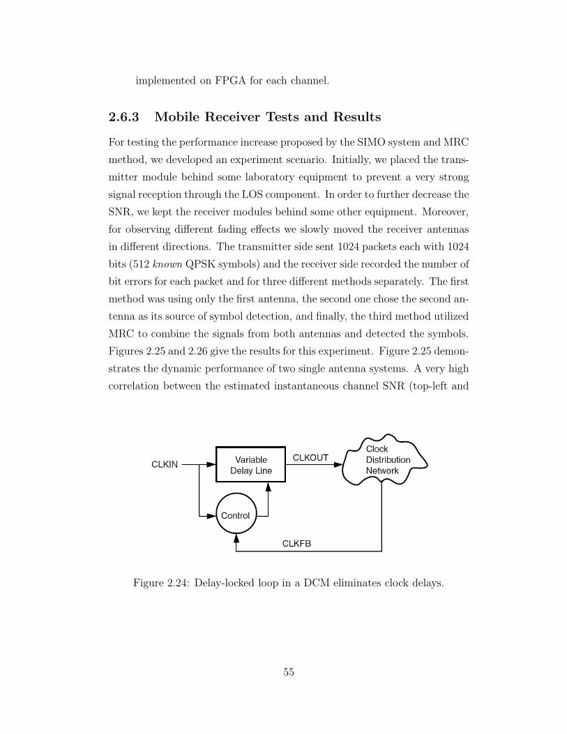
implemented on FPGA for each channel.
2.6.3 Mobile Receiver Tests and Results
For testing the performance increase proposed by the SIMO system and MRC
method, we developed an experiment scenario. Initially, we placed the trans-
mitter module behind some laboratory equipment to prevent a very strong
signal reception through the LOS component. In order to further decrease the
SNR, we kept the receiver modules behind some other equipment. Moreover,
for observing different fading effects we slowly moved the receiver antennas
in different directions. The transmitter side sent 1024 packets each with 1024
bits (512 known QPSK symbols) and the receiver side recorded the number of
bit errors for each packet and for three different methods separately. The first
method was using only the first antenna, the second one chose the second an-
tenna as its source of symbol detection, and finally, the third method utilized
MRC to combine the signals from both antennas and detected the symbols.
Figures 2.25 and 2.26 give the results for this experiment. Figure 2.25 demon-
strates the dynamic performance of two single antenna systems. A very high
correlation between the estimated instantaneous channel SNR (top-left and
Figure 2.24: Delay-locked loop in a DCM eliminates clock delays.
55

200 400 600 800 10000
5
10
15
20
1st Antenna Instantaneous SNR
Packet Number
Inst
anta
neou
s SN
R (
Eb /
N0),
dB
200 400 600 800 10000
5
10
15
20
2nd Antenna Instantaneous SNR
Packet Number
Inst
anta
neou
s SN
R (
Eb /
N0),
dB
200 400 600 800 10000
20
40
60
80
1st Antenna Instantaneous Bit Errors
Packet Number
Inst
anta
neou
s B
it E
rror
s
200 400 600 800 10000
20
40
60
80
2nd Antenna Instantaneous Bit Errors
Packet Number
Inst
anta
neou
s B
it E
rror
s
Figure 2.25: A deep fade results in increased bit errors in the bottom figures.
top-right figures) and the instantaneous bit error rate23 (BER) (bottom-left
and bottom-right figures) is trivially observed. Moreover, rapid variations in
the received SNR are observed for both antennas. Around the 600th packet,
the second antenna is in a deep fade and the BERs are very close to 0.1 for
these packets.
Fulfilling the expectations, Figure 2.26 proves the strength of two-antenna
system with MRC. The BER values for SIMO system never exceeds the
BERs of two single antenna detectors for the same packets. Moreover, since
the SNR values of the two received signals are summed for MRC, the SIMO
system does not observe a deep fade at any instance. As a result, using
MRC together with spatial diversity improved the performance of our testbed
definitely.
23Instantaneous BER stands for the number of bit errors in a given packet at any instant.
56

200 400 600 800 10000
5
10
15
20
MRC Instantaneous SNR
Packet Number
Inst
anta
neou
s SN
R (
Eb /
N0),
dB
200 400 600 800 10000
20
40
60
80MRC Instantaneous Bit Errors
Packet Number
Inst
anta
neou
s B
it E
rror
s
Figure 2.26: A deep fade (hence large number of bit errors) probability for
two-antenna system is very low.
57

chapter 3
pdsccc encoder/decoder
Channel coding can be defined as adding some redundant bits to a sequence
of bits that will be conveyed to a receiver, so that the discrepancies caused
by the noisy transmission medium can be mitigated. Also known as forward
error correction, channel coding aims the receiver side to correct the erro-
neous bits as much as possible. Related with the nature of the transmission
medium used, the coding technique to be used may be highly application
specific. For this reason, various types of coding techniques have been of-
fered for channels with bursts of errors, or with continuous thermal noise, or
with varying fading effects [11]. In the algebraic coding theoretical sense, we
can divide the codes into two families:
� Block Codes: Some examples include repetition codes, cyclic codes,
Reed Solomon codes, and BCH codes. They operate on fixed-size blocks
of bits (or symbols). Since not directly utilized in the scope of this thesis
research, block codes will not be detailed here.
� Convolutional Codes: Unlike block codes, they work on arbitrary
size bit (or symbol) sequences. They have encoders and decoders that
are relatively easier to implement when compared to block codes. More
information about their encoder and decoder structures is given in Sec-
tions 3.1 and 3.4.
One of the crucial steps in completion of our wireless testbed was includ-
ing appropriate encoding/decoding structures enabling efficient forward error
58

correction. Our main considerations on selection of appropriate coding tech-
nique included adequate hardware size to be implemented on our FPGA,
considerably small decoding time, easily scalable structure, and, certainly,
good performance within the SNR region of interest. Naturally, each one of
these listed requirements are in contradiction with the remaining ones and a
careful trade-off between them had to be made. After a careful investigation
in the literature we decided to implement a structure (PDSCCC) suggested
by one of the recent PhD. dissertations [10]. The reasons for selecting the
PDSCCC codes is clarified in the following sections together with essential
definitions; however, in the broadest sense, a parallel decodable serially con-
catenated convolutional code (PDSCCC) encoder is a hardware or software
which encodes its input bits making use of two (or more) groups of convolu-
tional encoders, where each group in itself operates in parallel. As expected, a
PDSCCC decoder carries out the reverse operation (decoding of the received
signals) within groups of parallel decoders in order to obtain the uncoded
bits back.
3.1 Convolutional Encoding
Convolutional encoding involves generating the output bits for an arbitrary
length of sequence of input bits according to a defined state transition mech-
anism. Convolutional encoders are of very simple structure and can be seen
as finite state machines which produce n output bits for given k input bits ac-
cording to their states and input bits at that instant. Here, k/n is called the
code rate of the convolutional code. There are two main building blocks
of a convolutional encoder: shift registers and binary addition operators
(XOR operators). The number of registers in each shift register block for
a convolutional code is usually shown by mi and the constraint length for a
convolutional encoder is defined as the max(mi + 1)1 [11]. Another parame-
1Note that there is one other definition which multiplies max(mi + 1) by the numberof output bits, n.
59

ter for convolutional codes is the minimum free distance, dfree, which is the
minimum Hamming distance between any two output sequences. Figure 3.1
demonstrates a convolutional encoder with single shift register block consist-
ing of two registers (shown by D, the delay elements), m1 = 2, one input
information bit, u, and two corresponding coded output bits, c1 and c2. This
encoder has 4 states, its constraint length is equal to three and its minimum
free distance is 5 [12]. The state diagram corresponding to the same encoder
is given in Figure 3.2. In addition to the state diagram representation,
Figure 3.1: A Rate 1/2 Convolutional Encoder.
there is one more representation method for convolutional codes which in-
cludes time information in addition to the information present in Figure 3.2.
60
This representation is known as the trellis diagram representation2 and the
trellis diagram representation for the rate 1/2 code in Figure 3.1 is given in
Figure 3.3 with the assumption that initial state and the final state for the
encoder is S0 (shown if Figure 3.2). It is quite common to make the convolu-
tional encoders start at state S0, and if we also force the last state to be S0
(as in Figure 3.3) with appropriate extra input bits, this approach is called
trellis termination(ending). We have used trellis termination for all encoding
processes defined in this thesis. The following VHDL code segments show
how easily re-configurable state and output tables can be constructed for
designing the convolutional encoder in Figure 3.1.
. . . (Firstly define basic properties of the convolutional encoder:
number of states, input bits, and output bits.)
constant states : integer := 4;
constant input bits : integer := 1;
constant output bits : integer := 2;
. . . (Define a state transition table which is a two dimensional
matrix with one row for each state and one column for each input
combination3. The entries are the next states when a row (cur-
rent state) and a column (input bit combination, here 0 or 1) are
given.)
type state matrix2D is ARRAY
(0 TO states−1, 0 TO 2**input bits−1)
OF integer range 0 TO states−1;
2Trellis diagram representation is especially helpful for decoding algorithms that utilizestate transition probabilities.
3In VHDL, (2��input bits−1) is equivalent to (2k − 1), k being the number of inputbits.
61

Figure 3.2: The input bit and the output bits for transition from one state
to other is shown on transition arrows in I/OO format. Here, Si corresponds
to the octal representation of i for the registers in the encoder, as an example
S1 stands for the register values 0 and 1 from left to right.
Figure 3.3: The state of the encoder turns back to 0th state (S0) after en-
coding this 7-bit input sequence.
62

. . . (Similarly define an output table of two dimensions, where
the entries are encoded bits for a given current state and a given
input combination.)
type output matrix2D is ARRAY
(0 TO states−1, 0 TO 2**input bits−1)
OF std logic vector(output bits−1 downto 0);
. . . (Now, instantiate (create) one instance for each of the tables
defined above. These instantiations will be directly used in the
convolutional encoder and also the decoder.)
constant state table : state matrix2D := ((0,2),
(2,0),
(3,1),
(1,3));
constant out table : output matrix2D := ((”00”,”11”),
(”00”,”11”),
(”01”,”10”),
(”01”,”10”));
. . . (Remaining part of the code follows.)
With these definitions very flexible encoder and decoder structures can be
implemented. Once a different encoder with different state transitions and
corresponding outputs is desired to be defined, the only change will be made
in these constant definitions. Especially for decoder structure, which is highly
complicated as given in Section 3.4, this improves the readability and the
reconfigurability of the design.
Convolutional encoders are classified with respect to the ways of genera-
tion of output bits. A convolutional encoder is said to be recursive whenever
an output bit effects the following states (hence output bits) through a feed-
63

back mechanism. Moreover, if the input bits of a convolutional decoder are
directly given as a part of the output bits, such encoders are called system-
atic. In the light of these definitions, the convolutional encoder in Figure 3.1
is both recursive and systematic. The code defined by this encoder is a maxi-
mal minimum free distance code for the codes of constraint length three [11],
and will be the basis of encoding and decoding procedures in the subsequent
sections. Hereafter, we will refer to this code (1,5/7) code in relation to its
generator polynomial written in octal form.
3.2 Serial Concatenation of Convolutional
Codes
In the search of codes that can achieve error-rate performance close to the
limits defined by Shannon with appropriate decoding complexity, many the-
orists tried to combine the best properties of different codes in a single code.
In one of the initial trials [16], concatenation of a Reed Solomon code with a
simple convolutional code gave rise to various descendants with some other
forms of concatenation. A form of serial concatenation of two convolutional
codes with an interleaver structure in between is suggested in [15]. In 1993,
a new class of codes with parallel concatenation of convolutional codes con-
nected by a specially designed interleaver was introduced [17]. These par-
allel concatenated convolutional codes (PCCCs) are also called turbo codes.
Subsequent research carried on the serially concatenated convolutional codes
(SCCCs) provided some similarities of these codes with the PCCCs. In addi-
tion to the analogy between these two types, under some special conditions
SCCCs are proved to have better bit error rate (BER) performance than the
same rate PCCCs. In [13], SCCCs outperform PCCC counterparts under
many scenarios for frequency-nonselective Rayleigh fading channels. Also
in [14], it was found that SCCCs may have smaller changes in their slope of
bit error curves than the PCCCs, which makes PCCCs reach their error floor
64

before the SCCCs. This property of SCCCs may be utilized where extremely
low BER values are needed.
Essentially, an SCCC is composed of two convolutional codes. The en-
coder encoding the information bits initially is called the outer encoder. The
second one that encodes the output of the outer encoder is named as the in-
ner encoder. Inner encoders usually take their input in an interleaved fashion
instead of directly reading the outputs of the outer encoders. The structure
of a SCCC is presented in Figure 3.4. Effectively, the inner and outer en-
Figure 3.4: Structure of a serially concatenated convolutional code.
coders may have different coding parameters, and the overall rate for SCCC
is the multiplication of their rates. The interleaver size, N, is determined by
the number of information bits (uo) and the rate of the outer encoder (ko/no)
(N = length(uo) ko
no). The reasons and details for interleaver implementation
will be given in Section 3.2.1.
3.2.1 Interleaving
Interleaving of a given data sequence requires moving each data element into
another place in the sequence such that there is a one-to-one mapping be-
tween the initial and the final places. As described in Section 2.6.1, wireless
channels are usually prone to fading problems, which may result in consecu-
65

tive bit errors in the reception. Appropriately designed interleavers distribute
the elements in error in great distances from each other so that the errors
can be seen as independent when observed from the output of the inter-
leaver. Moreover, they are capable of distributing the errors occurred in the
first stage of a decoding process onto many data elements that will be pro-
cessed by the next stages. Furthermore, interleaving can also be utilized to
reduce the number of low weight codewords and increase the minimum free
distance [10].
There are various types of interleavers that are used under different con-
ditions. Block interleavers, convolutional interleavers, random interleavers,
code-matched interleavers are some examples to be given. Our main inter-
est is on the S-random interleavers for the design of interleaver that will be
utilized in both the encoder and the decoder structures. An S-random inter-
leaver maps its input place order to an output place order according to two
rules:
� Firstly, all the mappings are determined randomly, with equal chance
of selection for each output place order.
� The randomly selected order is accepted only if it is in a distance greater
than S for all of the S previously selected orders. Otherwise, it is not
accepted and a new random order is generated, until this condition is
satisfied.
The parameter S is a predetermined integer and it usually satisfies S ≤√K/2, K being the interleaver size [18]. S-random interleavers have good
spreading properties when compared to other types and provide good BER
performance when used with convolutional codes. Its implementation details
in our testbed are listed in Section 3.3.1 following the specific parallelized
encoder structure.
66
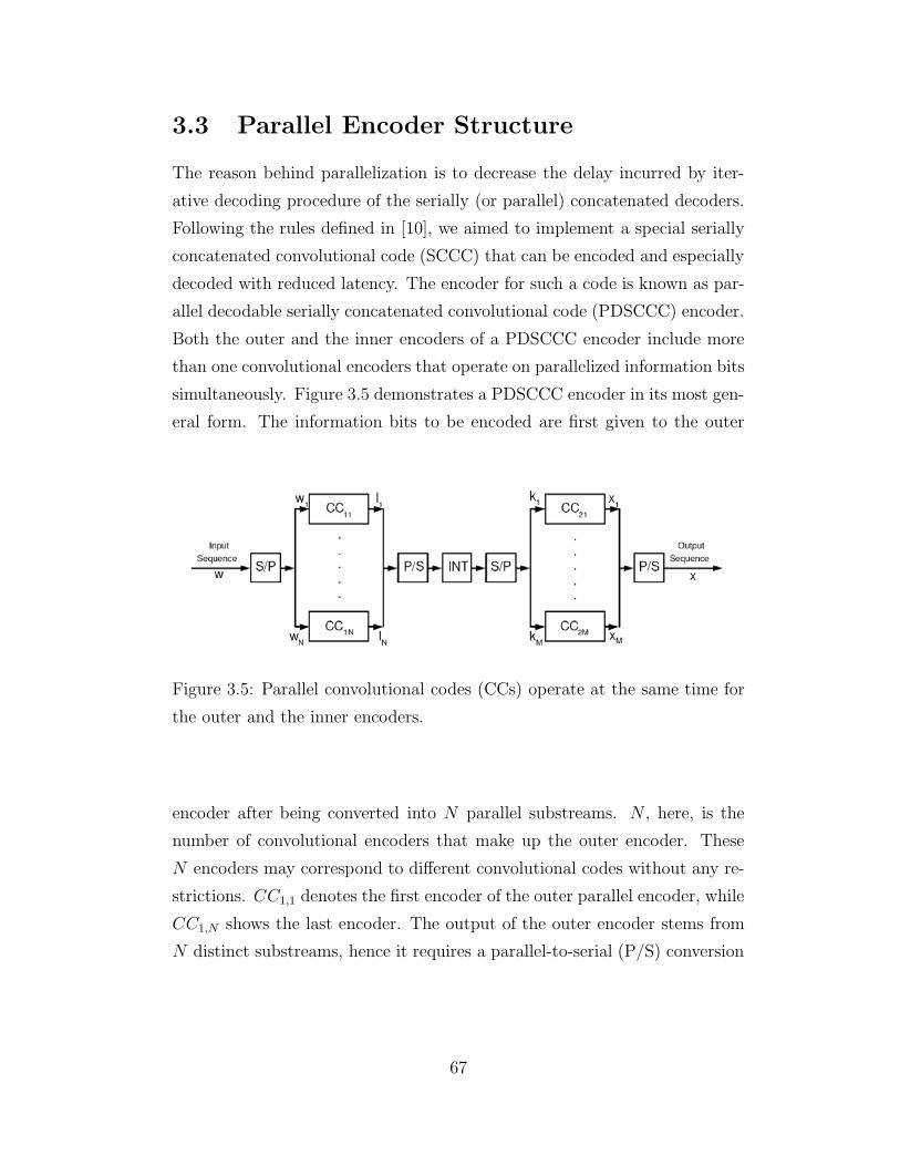
3.3 Parallel Encoder Structure
The reason behind parallelization is to decrease the delay incurred by iter-
ative decoding procedure of the serially (or parallel) concatenated decoders.
Following the rules defined in [10], we aimed to implement a special serially
concatenated convolutional code (SCCC) that can be encoded and especially
decoded with reduced latency. The encoder for such a code is known as par-
allel decodable serially concatenated convolutional code (PDSCCC) encoder.
Both the outer and the inner encoders of a PDSCCC encoder include more
than one convolutional encoders that operate on parallelized information bits
simultaneously. Figure 3.5 demonstrates a PDSCCC encoder in its most gen-
eral form. The information bits to be encoded are first given to the outer
Figure 3.5: Parallel convolutional codes (CCs) operate at the same time for
the outer and the inner encoders.
encoder after being converted into N parallel substreams. N , here, is the
number of convolutional encoders that make up the outer encoder. These
N encoders may correspond to different convolutional codes without any re-
strictions. CC1,1 denotes the first encoder of the outer parallel encoder, while
CC1,N shows the last encoder. The output of the outer encoder stems from
N distinct substreams, hence it requires a parallel-to-serial (P/S) conversion
67

operation before the interleaving operation. Following the interleaver, whose
implementation rules will be given in Section 3.3.1, the data bits have to be
converted into M parallel substreams (k1 to kM) which will be encoded by
M convolutional encoders of the inner parallel encoder. The structure for
the parallel inner encoder is analogous to the outer one.
In the testbed, the numbers N and M are both chosen as 4 for initial
experiments. The length of the information bit sequence (length of W in
Figure 3.5) is taken as 128 in order to keep the final encoded bit length
(length of X) within the limits of the testbed packet length. All of the con-
volutional encoders are selected to encode their input bits using the (1,5/7)
code defined in Section 3.1. According to these assumptions, the input se-
quence for CC1,i is 32 and with two trellis termination bits, each CC1,i yields
2× (32 +2) = 68 encoded bits. Therefore, the interleaver is required to have
length 4 × 68 = 272, which is a small number when we compare the perfor-
mance of serially concatenated encoders with different interleaver sizes [10].
This issue is discussed in Chapter 5. Another point in relation to interleaving
is that this operation should not take up extra time and extra storage area
for FPGA implementation. In other words, the encoders within the inner
parallel encoder should read their input in an interleaved fashion from the
output substreams of the outer parallel encoder directly. As a result, each
inner level encoder (CC2,1 to CC2,4) should keep one table describing the
substream number and the order of the bit in that substream for each bit it
will encode. Keeping such tables for the inner level encoders, we can combine
the tasks P/S, interleaving, and S/P in one process. This idea comes with
its cost in the implementation as expected. First of all, we have to keep
4 68-entry tables that store the addresses revealing how the inner level en-
coders will take their inputs. Moreover, we have implemented the outer and
the inner decoder using the same hardware resources since they are identical
in nature (both have 4 identical (1,5/7) convolutional encoders) and they
operate in a well-defined order (one is non-operational when the other one is
encoding data). This reusage of encoders diminished the logic area require-
68

ment. However, when we imposed an interleaved reading task for the inner
encoder, the similarities between the two structures decreased leading to ex-
tra control logic for handling both interleaved and non-interleaved reading
operations on a single architecture. The interleaved reading process involves
one extra clock cycle for firstly grasping the address of the data to be read.
This extra delay should also be treated with great care in the design of the
PDSCCC decoder which is detailed in Section 3.5.2.
Each inner level encoder output consists of 2 × (68 + 2) = 140 encoded
bits, which add up to 560 bits for M = 4 encoders. Finally, these 560 bits
are stored in a packet which is initiated by the 13-bit Barker sequence for
synchronization and channel equalization purposes.
3.3.1 Memory Collision-Free Interleavers
The interleaver structure introduced in Section 3.2.1 is further detailed in this
chapter. The basic structure for our implementation of PDSCCC interleaver
depends on the S-random interleavers. However, a subclass of this type of
interleavers is to be defined for efficient utilization in the PDSCCC encoder
and the PDSCCC decoder. From the viewpoint of design rules for S-random
interleavers, it is very likely that two or more inner level encoders (trying to
read the encoded outputs of a single outer level encoder at the same time)
will lead to memory collisions. There is no rule for S-random interleaver
generation that will restrict the usage of the same output RAM of an outer
convolutional encoder by more than one inner convolutional encoders. Fig-
ure 3.6 shows how an S-random interleaver causes memory collision in the
first encoding cycle of the inner encoder. The address tables for the inner
level encoders are shown in the middle. For example, the first inner level
encoder (CC2,1) will read the 1st output bit of the first outer level encoder
(CC1,1) initially, then it will read the 1st output bit of the second outer level
encoder (this address is 5), then the 1st output bit of the third outer level
encoder (its address is 9) and finally the 1st output bit of the fourth outer
69

Figure 3.6: All of the 4 inner level decoders try to read from RAM0 in the
first encoding interval.
level encoder. Similarly, the second inner level encoder will read the 2nd out-
put bit of the first outer level encoder initially. Hence, both the first and the
second inner level encoders will try to access the same RAM, namely RAM0,
which stores the encoded outputs of the first outer level encoder. In addition
to these, the third and the fourth inner level encoders will also try to read
from RAM0. Although the Block RAM resources on ML310 FPGA board
are capable of being read from two distinct addresses at the same time, four
accesses at the same time can not be handled.
Therefore, it is desired to define a new subclass of S-random interleavers,
which are named as row-column S-random (RCS-random) interleavers in [10],
so that memory collisions during interleaved reading can be avoided. An
RCS-random interleaver is made up of many smaller S-random interleavers
working on different parts of the whole data to be interleaved. Firstly, the
data in each RAM (that is each output sequence of outer level encoders) are
70

S-random interleaved, which corresponds to interleaving the rows of the whole
data. In our case, this means building 4 distinct S-random interleavers, all of
which are of size 68. This row interleaving is followed by interleaving within
the same addresses of RAMs (column interleaving). In column interleaving,
the data bits in the first addresses of (N = 4) RAMs are interleaved by an
S-random interleaver4, the ones in the second addresses by another S-random
interleaver, and so forth for all the 68 addresses. It is easy to prove that such
an interleaving procedure will not cause memory collisions by just analyzing
the resulting interleavers after row interleaving and after column interleaving
separately:
� If the given structure is memory collision-free, just applying row in-
terleaving to each row separately will not cause memory collisions to
appear, since simply arranging rows (RAM0, RAM1, . . . ) within them-
selves results in all the inner level encoders reading from distinct RAMs
for all encoding instances. (CC2,1 from the first RAM, CC2,2 from the
second RAM, . . . ).
� If the given structure is memory collision-free (it is true for the output
of row interleaving operation), just applying column interleaving to
each address of RAMs, will not alter the one-to-one mapping property
between the inner level encoders and the RAMs, but only change the
one-to-one mapping to another one-to-one mapping.
These steps are exemplified in Figure 3.7, where an RSC-random interleaver
is obtained at the bottom from the ordered table in the top-left corner. The
operation of this RCS-random interleaver at the first interleaving instant is
shown in Figure 3.8. At the first encoding interval each CC2,i reaches a
distinct RAM and this is true for all remaining encoding intervals as well.
In order to implement an RCS-random interleaver of size 4 × 68 = 272,
we initially prepared 4 S-random interleavers of size 68 in MATLAB. In
4In fact, with N = 4, S-random interleaver reduces to purely random interleaver.
71

Figure 3.7: Firstly the rows are interleaved, then the columns [10].
this step, S was taken as 5. In the second step we built up 68 S-random
interleavers of size 4 in a similar fashion, with S is equal to 1. Then, a
conversion code for translating these interleaved address information from
integers to binary representation was written. This code gave the addresses
of the interleaved bits within a RAM together with the selected RAM number
for that interleaving. The convention for addressing is : “The first two bits
in the interleaving table give the RAM number from which data bit is to
be read. Remaining 7 bits are used for addressing within the RAM selected
by the first two bits”. The storage of these addresses is realized by using
4 Block RAMs as read-only memories (ROM) with 68 entries of 9-bit data
width. As the final step of PDSCCC encoder implementation, the encoded
bits of length 560 are compared with the output of PDSCCC encoder written
72

Figure 3.8: At each time step, each encoder reads from a distinct RAM.
in MATLAB. Table 3.1 presents some figures for hardware complexity of the
implemented PDSCCC encoder. It is possible to neglect the area used by
the encoder, however the Block RAM usage may be important in case of
a larger PDSCCC encoder design with more convolutional encoders in the
inner and/or outer encoders.
3.4 Marginal a Posteriori Decoding
Two types of decoding algorithms are very popular for convolutional codes.
The first type of algorithms find a codeword, v, for a transmitted codeword,
73

Table 3.1: PDSCCC Encoder Synthesis Results
Unit Name Usage Count and Percentage
Number of Slices 282(2%)
Number of Slice Flip Flops 138(0.5%)
Number of 4 input LUTs 515(1.5%)
Number of BRAMs 5(3.5%)
Maximum Operating Frequency 202.192 MHz
v, and the received sequence, r, such that the likelihood function is max-
imized. Hence, they are called as the maximum likelihood (ML) decoding
algorithms. Viterbi algorithm is an example of ML algorithms, which can
find the most likely sequence (or path) with only linear decoding time in-
crease as the sequence length increases. In this sense, Viterbi algorithm is
word error rate (WER) minimizing (P(v �= v | r) is minimized). The second
type of popular algorithms aim to minimize the bit error rate (BER) through
maximization of the marginal a posteriori (MAP) probabilities for the trans-
mitted information bit ul, P(ul = ul | r), where ul is the decoded information
bit. They are named as MAP algorithms and the best known example to
MAP algorithms is the BCJR algorithm [4]. When the probabilities for hav-
ing ul = 1 and ul = −1 are equal, two algorithms are equivalent and Viterbi
algorithm is preferable due to its lower complexity. However, when the bit
probabilities are different BCJR algorithm performs better than Viterbi al-
gorithm. Good examples for having unequal bit probabilities can be iterative
decoding algorithms. During the iteration steps the likelihood assigned to
each bit is updated and next steps use unequal bit likelihoods in general.
Since PDSCCC decoder use iteration for achieving lower BER values, it is
inevitable for PDSCCC decoder structure to utilize BCJR algorithm.
Without deriving the equalities, simply the variables used in BCJR al-
gorithm will be defined here. The detailed derivations are presented in [12].
74

We will start with the definition for the a posteriori log-likelihoods (LL) of
the information bits. LL values are defined as,
LL(ul) ≡[
P (ul = 1 | r)P (ul = −1 | r)
]. (3.1)
Then, a bit is decided as 1 whenever LL value corresponding to it is positive
after the last iteration step. Otherwise, it is decided as a −1. The definition
for the α metric, which is obtained by a forward iteration on the received
sequence, is given as,
αl(s′) ≡ p(s′, rt<l). (3.2)
Therefore, α metric can be defined as the probability of being at state s′ and
having a received sequence rt<l upto time l. Similarly, γ (branch) metric is
defined for the probability of having a state transition from s′ to state s at
time l with received sequence value of rl given s′. Hence, γ metric is given
as,
γl(s′, s) ≡ p(s, rl | s′). (3.3)
The backward metric, which is calculated over the received sequence in back-
wards direction, is known as β metric and defined as,
βl+1(s) ≡ p(rt>l | s). (3.4)
After some steps on α and β metric it is easily found that both metrics’
calculations can be written in recursive equations as,
αl+1(s) =∑s′∈σl
γl(s′, s)αl(s
′), (3.5)
βl(s′) =
∑s∈σl+1
γl(s′, s)βl+1(s). (3.6)
In Eqns. 3.2 and 3.4, the sets σl and σl+1 denote the sets all possible states
from (to) which a transition is possible at time l (l + 1). For our PDSCCC
decoder, since all of the (1,5/7) convolutional codes have 4 states, for ob-
taining a new α or β metric we have to carry out 4 multiplications and a
75

summation of these results. The basic steps for these recursive calculations
are related to the S0 state assumption for the initial state of all encoders
and the trellis termination that identifies the final state as S0. The initial
assignments for α and β metrics are given as,
α0(s) =
{1 s = 0
0 s �= 0, (3.7)
βK(s) =
{1 s = 0
0 s �= 0. (3.8)
In Eqn. 3.8, K denotes the number of information bits to be decoded by
the BCJR decoder. If the γ metric given in Eqn 3.3 is analyzed with the
assumption that noise signal in the received signal is additive white Gaussian,
it can be simplified in terms of channel reliability factor (Lc) and a priori bit
probability (La(ul)) as,
γl(s′, s) = eulLa(ul)/2e(Lc/2)(�rl ·�vl). (3.9)
In Eqn. 3.9, we have two factors determining the branch metric. One is the
a priori bit probability, which is found by the previous iteration step5. The
other one is the inner product of received vector at time l, rl, and output
vector for the transition from state s′ to state s, vl. This inner product result
is scaled by Lc/2 = 2Es/N0, which corresponds to multiplying it by a larger
number when the symbol SNR is high. Therefore, with BCJR algorithm,
observations are trusted more when the SNR is high, otherwise a priori values
are utilized more in finding the updated branch metrics (and also updated
LL values). This requires estimation of the received SNR to be used in
the PDSCCC decoder. In Section 2.5.5, a method for estimating the signal
power and the noise power is given. Using that method the estimated SNR
may be multiplied by 2rl for removing the multiplication operation from the
PDSCCC decoder. However, simply that removal is not enough, there are
5If no previous steps exist, La(ul) is initialized as 0 for all l = 0, 1, . . . , K − 1.
76

many multiplication operations in Eqns. 3.5, 3.6, and 3.9. In order to simplify
these calculations, log-domain metrics can be defined as,
γ�l (s
′, s) ≡ ln γl(s′, s) = ulLa(ul)/2 + (Lc/2)(rl · vl), (3.10)
α�l+1(s) ≡ ln αl+1(s) = ln
∑s′∈σl
eγ�l (s′,s)+α�
l (s′), (3.11)
β�l (s
′) ≡ ln βl(s′) = ln
∑s∈σl+1
eγ�l (s′,s)+β�
l+1(s). (3.12)
Now the metric calculation for γ is greatly simplified, whereas the calculations
of α and β metrics still involve “ln” operation over summation of 4 elements,
since convolutional encoders have 4 states in our case. This complication can
be solved by using the identity,
max�(x, y) ≡ ln(ex + ey) = max(x, y) + ln(1 + e−|x−y|). (3.13)
With max� operator instead of implementing a two-dimensional lookup table
for approximating ln function of two variables x and y, a single dimension
table using the absolute difference of x and y, and a maximization operator
is implemented. Moreover, max� can be defined for more than two operands
as,
max�(x1, x2, . . . , xp) =max�(x1, max�(x2, x3, . . . , xp)) (3.14)
...
=max�(x1, max�(x2, . . . , max�(xp−1, xp)) . . .)) (3.15)
Using Eqn. 3.14, we can rewrite forward and backward metric calculations
as,
α�l+1(s) =max�
s′∈{S0,S1,S2,S3} [γ�l (s
′, s) + α�l (s
′)] , (3.16)
α�0(s) =
{0 s = S0
−∞ s �= S0, (3.17)
β�l (s
′) =max�s∈{S0,S1,S2,S3}
[γ�
l (s′, s) + β�
l+1(s)], (3.18)
β�K(s) =
{0 s = S0
−∞ s �= S0. (3.19)
77

The max� operations in Eqns. 3.16 and 3.18 can be implemented by firstly
taking two groups of two operands into two max� operators with the defini-
tion in Eqn. 3.13, then applying the same max� operator on the results of
the first stage. For this way of metric calculation, three max� operators are
required for single αl�(s) or βl
�(s) value. Since there are 4 states, in total
(4 × 2 × 3 = 24) max� operators need to be implemented. This may be the
bottleneck for optimizing the logic area utilized by the PDSCCC decoder.
The solution proposed for max� implementation is given in Section 3.5.5.
This version of the BCJR algorithm (calculating the metrics in the log-
domain) is also known as log-MAP algorithm. The final expression for
PDSCCC implementation is on the LL values for information bits and given
as,
LL(ul) = ln
⎡⎣ ∑
(s′,s)∈δ+
eβ�l+1(s)+γ�
l (s′,s)+α�l (s′)
⎤⎦ (3.20)
− ln
⎡⎣ ∑
(s′,s)∈δ−eβ�
l+1(s)+γ�l (s′,s)+α�
l (s′)
⎤⎦ ,
=max�(s′,s)∈δ+ [β�
l+1(s) + γ�l (s
′, s) + α�l (s
′)] (3.21)
−max�(s′,s)∈δ− [β�
l+1(s) + γ�l (s
′, s) + α�l (s
′)].
The δ+ and δ− given in Eqns. 3.20 and 3.21 denote the sets of transitions
made by an information bit 1 and −1 respectively. Consequently, for calcu-
lating a single LL value of an information bit two 4-input max� operators,
or equally 6 two-input usual max� operators are required in a single MAP
decoder.
3.5 Fast PDSCCC Decoder
The decoding algorithm to be used as the basis for construction of PDSCCC
decoder is given with its essentials in Section 3.4. Now, in this section, more
78

implementation details about the MAP decoder and interconnection rules for
inner and outer decoder structures will be explained.
Firstly, the decoder structure for a serially concatenated code is composed
of four main building blocks. It includes an inner decoder (corresponding to
the inner encoder in serial concatenation), an outer decoder (corresponds to
the outer encoder), an interleaver with the same properties as in the serially
concatenated encoder part, and a deinterleaver which supports the feedback
between the outer decoder and the inner decoder for iterating over the re-
ceived sequence many times. These main building blocks together with some
additional blocks are shown in Figure 3.9. The decoder of a serially concate-
Figure 3.9: Interleaver and the corresponding deinterleaver connect the inner
and outer decoders.
nated convolutional code (SCCC) resembles that of a parallel concatenated
convolutional code (turbo code). The main distinctions between two types
of decoders lie in two points:
� The way outer decoder of a SCCC decoder takes its channel informa-
tion and the a priori information is different from the way of lower
and upper decoders of a turbo decoder. The outer decoder does not
directly take its channel information from the channel, but this input is
79

supplied by the inner decoder as the log-likelihood (LL) values (for x in
Figure 3.9). Also the a priori information of the uncoded information
bits (u) are always zero for outer decoder, since it has no knowledge
on these uncoded bits. It also gives its coded output estimates (L(x))
to the inner decoder since these are the uncoded bit LL values for the
inner decoder.
� Both the inner and the outer decoders subtract only the information
taken from the other decoder from their estimated outputs. This is
not the case for turbo decoding where both of the decoders subtract
the channel information from their estimates, too. Here only one of
the decoders (inner decoder) directly observe the channel and this will
not result in divergence of the metrics due to accumulation of channel
information.
The construction of the parallelized SCCC (PDSCCC) decoder is similar
to the construction of PDSCCC encoder from the SCCC encoder structure.
An illustrative diagram for a PDSCCC decoder is provided in Figure 3.10.
As with the PDSCCC encoder, for PDSCCC decoder the number of sub-
Figure 3.10: Parallelized convolutional decoders speed up the decoding op-
eration for both the inner and the outer decoding [10].
80

decoders in both the inner and the outer decoders is taken as 4. Therefore,
each encoder in the inner encoder will take (560/4 = 140) bits of received
sequences. They will provide output estimates for (140/2 − 2 = 68) bits
without any need for estimating the trellis ending bits used in the inner
encoder of PDSCCC encoder. After being deinterleaved, these (4 × 68)-bit
LL values will be given to the outer encoder. Outer encoder will provide not
only the LL values for (68/2 − 2 = 32) uncoded information bits, but also
the a priori information for 4× 68 bits to the inner decoder back, which will
read these data in an interleaved fashion. This iteration is carried out for
a pre-defined or adaptively chosen number of times and only then will the
hard decisions for the uncoded bits be given using the uncoded information
bit LL value output of the outer decoder. The following sections will provide
information about critical parts of PDSCCC implementation on FPGA and
list a number of improvements for faster operation and reduced hardware
size.
3.5.1 Simultaneous Calculation of Alpha and
Beta Metric Values
If the branch metric calculations in Eqns. 3.16 and 3.18 are considered, two
operations, i.e., calculation of α and β metrics, are independent from each
other so that simultaneous evaluation of α metric values in forward direction
and β metric values in backward direction is possible. This will bring an
advantage in decoding latency only if the LL values are determined during
these calculations, because there are currently known algorithms which yield
the LL values after making two sweeps over the received vector [19, 20]. The
idea for obtaining the LL values with just one sweep depends on calculating
the LL values at the first possible instant. As an example, assuming LL
values for 70 information bits will be found, consider that the first metric
values, α�0(s) and β�
70(s), are written to corresponding places at time 0 as
in Figure 3.11. In the following cycle using the α�0(s) and the γ�
0(s) values
81

Figure 3.11: α and β metric RAMs are initialized at time 0.
α�1(s) values will be obtained for each state s. Similarly, β�
69(s) values will
be calculated and written to next place, 69th place, in β metric RAMs as in
Figure 3.12. In the next cycles, both of the metrics will be calculated in the
Figure 3.12: Metric calculations continues at time 1 with second values.
directions shown by arrows. Remembering Eqn. 3.21 for LL value calculation,
for finding LL(ul) the required metrics are α�l (s), γ�
l (s), and β�l+1(s). Hence,
the earliest calculation of an LL value is possible at time 35, after the α and
82

Figure 3.13: At time 35, first LL values are ready to be calculated.
β metric calculations meet at the midpoint. In fact, at this instant two LL
values, namely LL(u35) and LL(u34), are calculated. This first LL calculation
instant is given in Figure 3.13. Following this cycle two LL values are found
in each cycle and at the end after 70 cycles, with just one sweep over the
received vector, all LL values are calculated as in Figure 3.14 Especially, for
Figure 3.14: Finally, after time 69, all LL values are obtained.
iterative decoding algorithms decoder latency is the bottleneck for increasing
83

the iteration number. Our implementation improves the decoding latency of
each iteration step by halving it.
3.5.2 Interleaving and Deinterleaving Operations
As it is given in Figure 3.10, various S/P, P/S converters, subtractions for
obtaining extrinsic information, and interleaving/deinterleaving operations
exist in a PDSCCC decoder. In Section 3.3, the interleaving operation is de-
fined such that the inner encoder reads from substreams of the outer encoder
output so that P/S converter, interleaver, and S/P converter are joined in a
single structure with just one cycle delay. The same interleaver is used for
reading the LL outputs (extrinsic information) of the outer decoder as well.
However, a deinterleaver which combines the jobs of P/S converter, deinter-
leaver, and S/P converter in Figure 3.10 is still required. Implementing new
address (deinterleaving) tables for each output level decoder to read its input
from the output substreams of the inner level decoders will be very costly
in terms of Block RAM usage. Just as in the case of interleaver tables, 4
seperate ROMs will be made out of Block RAMs. In fact, there is no need for
deinterleaver tables if we can observe this operation from the point of inner
decoder. An inner level convolutional decoder, knowing which address it has
read its a priori information from, can write its extrinsic information output
(after subtraction) LL value just to the same address. This operation force
all inner level decoders to maintain last reading addresses from the outputs
of the outer level decoders and writing its LL result to the same address
in already a deinterleaved fashion. Therefore, the deinterleaving job is also
given to the inner decoder, while the outer decoder reads and writes in a
sequential manner. It must be emphasized that since we have simultaneous
calculation of α and β metrics as described in Section 3.5.1, two LL values
are written to LL value RAMs at each instance once the midpoint of the data
is passed. This is easily handled by defining LL RAMs as dual port Block
RAMs, however, the γ calculation described in Eqn. 3.10 requires reading of
84

two consecutive received values (for one information bit two encoded bits are
sent). When the simultaneous calculation of forward and backward metrics
is also considered, at any instant outer decoder requires to read 4 extrinsic
information values (from the output of the inner decoder) at the same time.
It may be proposed that having two consecutive extrinsic information in the
same word (address) of the inner decoder output RAMs is enough for so-
lution. On the contrary, these consecutive extrinsic information values are
written at different times by the inner decoder since they are not consecu-
tively found. The only solution is to keep the extrinsic information values
of the information bits and their parity bits in separate RAMs for the outer
decoder input. In total, 8 Block RAMs of size 34-word6 are desired. This
problem does not exist for the outer decoder output since it writes its out-
put LL values (a-priori information for inner encoder) sequentially and inner
decoder just reads these values (in an interleaved fashion) with no write op-
erations. The memory requirement at the output of the outer decoder is 4
Block RAMs of size 34-word7. The Figure 3.15 demonstrates the placement
of these LL value storage RAMs.
3.5.3 Re-usage of Parallel MAP Decoders
Due to serial concatenation, the inner and the outer decoders operate in
succession. Inner decoder does not operate on the received data while the
outer decoder is processing the received data, and vice versa. This is a great
opportunity for reducing the logic area utilized by the PDSCCC decoder.
However, this reusable architecture has its own problems which should be
handled separately:
� The reading and writing of LL values for the inner and the outer de-
coders differ. Inner decoder can always read and write with one clock
6Each word is a single LL value.
7Here, each word is a combination of two LL values.
85

Figure 3.15: All the interleaving (during reading) and deinterleaving (during
writing) operations are carried out by inner level decoders (D2,1 to D2,4) over
a single address table.
cycle delay due to interleaving and deinterleaving. On the other hand,
outer decoder reads and writes by directly addressing the RAMs of
interest.
� The inner and the outer decoders read from different RAMs and write
to different RAMs. The inner decoder reads from received data vector
RAMs and outer decoder output RAMs, it writes to 8 distinct output
RAMs. The outer decoder only reads from inner decoder output RAMs
and writes to 4 distinct output RAMs.
� The a priori log-likelihood input of the outer decoder is connected to
zero, whereas the inner decoder accepts a priori information from the
coded LL output of the outer decoder.
� The lengths of input and output sequences for two decoders are not
equal. Each inner level convolutional decoder operates on a received
vector of 140 values and gives 68 LL values corresponding to its uncoded
bits as the output. In contrast, for the output level decoders the input
size is 68 and output sizes are 68 for coded LL values and 32 for uncoded
86
LL values. Since the input lengths are different the midpoints (after
which LL calculation will begin) are also different for two decoders.
Therefore, it is clear that reusing the modules for implementing both the in-
ner and the outer decoders increases complexity of the PDSCCC decoder de-
sign, although a great size reduction is obtained. All convolutional decoders
must know whether they operate as an inner decoder or an outer decoder
constituent block. When combined with the interleaving/deinterleaving and
information subtraction procedures, reusing modules results in highly com-
plicated control logic modules. Consequently, the maximum combinational
delay of the PDSCCC decoder increases leading to lower operating frequen-
cies. Although our final operating frequency is above the desired levels (see
Section 3.7.1 for exact values), some optimization methods for further im-
proving the clock frequency of PDSCCC decoder is given Chapter 5.
3.5.4 Alpha, Beta, Gamma Metric Size Selection and
Metric Storage Allocation
The α, β, γ metrics, and LL values are represented by fixed point numbers
on FPGA for simplified operations in 2’s complement logic. It is easy to
see that there is a trade-off between the metric size (number of bits used
representing metrics) and the hardware complexity of the PDSCCC decoder,
which consists of 4 BCJR decoders in our case. It is shown in [21] that using
8-bit quantization for representing the metric values in log-MAP algorithm
yields such a good performance that almost no SNR loss is incurred with
respect to the floating point utilization for the metrics. It is also observed
in [21] that 4-bit quantization results in an SNR loss of approximately 0.1dB
for most simulation cases. Hence, we decided to have a PDSCCC decoder
with parametrizable metric size and a parametrization interval of 4-bit to
8-bit quantization. Moreover, the ideal metric size is determined as 6-bit
when the hardware size, operation frequency, and SNR loss are considered
as the constraints of the system. 8-bit quantization is an upper limit when
87
the PDSCCC decoder size is constrained to fit into the used ML310 FPGA
board. Especially, when the multiple-antenna system with more than two
receiver antennas is the destination of future testbed implementation, some
optimization will be required for this 8-bit quantized architecture.
Each inner level decoder utilizes single Block RAM for storing both of the
α and the β metrics. This optimization is possible only with simultaneous
calculation of two metrics. Once the middle point for calculation of the
metrics is left behind LL values can be calculated, thus there is no more
need for storing new α and β values. Newly found values will be directly
used in the next clock cycle for LL value calculation. In this way, the α
and the β metric storage RAMs shown in Figure 3.11 can be merged into a
single RAM, in which the first half is reserved for storing (α�0,. . . , α
�34) and
the second half is reserved for (β�36,. . . , β
�70). This optimization is novel to the
knowledge of the author of this thesis and it reduces the total RAM usage by
the number of parallel decoders in the inner decoder, which results in saving
4 Block RAMs (or more for metric sizes larger than 4-bit). Since the outer
level decoders are physically the same decoders as the inner level decoders,
no more RAM utilization is required for the outer decoder. The αl(s = S0),
αl(s = S1), αl(s = S2), and αl(s = S3) values are stored in the lth address of
a Block RAM, whose size is parametrically tuned for housing 4 α (or equally
β) values next to each other.
Both the inner and the outer level decoders have to store γ metrics for
all possible transitions at any instant. With a 1/2-rate and 4-state code, this
corresponds to storing 8 possible transitions for γl(s′, s). Due to this large
number and some other practical implementation issues, log-likelihoods for
the transitions made as a result of an information bit 1 are stored in a separate
RAM than the ones as a result of an information bit −1. Therefore, single
decoder uses two Block RAMs for the storage of γ metrics. Similar to α-β
storage 4 γ values for same information bit are kept in a single word of a
Block RAM, occupying the same address.
88

3.5.5 Max� Approximation Method
The max� expression given in Eqn. 3.13 involves two terms: the maximiza-
tion term (max(x, y)) and the nonlinear correction function fc(| x − y |) =
ln(1 + e−|x−y|). The maximum finding operator is fairly easy for FPGA im-
plementation, however fc(| x− y |) is the problematic part in max� operator
implementation. In [19], four methods of approximating the correction func-
tion are listed and a BER performance comparison is made. These methods,
three of which are shown in Figure 3.16, are:
� Max-log-MAP approximation: This is the simplest method which
totally neglects the effects of the correction function. In other words,
(fc(| x − y |) = 0) is accepted for all (x, y) pairs. Therefore, it is not
shown in Figure 3.16. It leads to worst BER performance as expected.
� Constant log-MAP approximation: This algorithm takes the cor-
rection function as a constant value for values of | x− y | smaller than
a given value and as zero elsewhere.
� Linear log-MAP approximation: The correction function is ap-
proximated by a piece-wise linear function in this approach. The ap-
proximation function is given as,
fc(| x − y |) ≈{
0 if | x − y |> T
a(| x − y | −T ) if | x − y |≤ T. (3.22)
Minimization of mean-square error for this approximation yields a =
−0.24904 and T = 2.5068. This is one of the most common methods
in implementation of max� operator.
� Lookup table approximation: The performance of this method is
heavily dependent on the depth and the width of the lookup table
used. The Figure 3.16 demonstrates an approximation over 30 samples
evenly spaced in the significant part of the exact correction function. It
closely approximates the desired shape, however implementation cost
89

of a such a large lookup table is high and it is not preferable in case
many instances of max� operator exist.
0 0.5 1 1.5 2 2.5 30
0.1
0.2
0.3
0.4
0.5
0.6
0.7Methods for Approximating the Correction Function in max� Operator
| x − y |
f c(|
x−
y|),
the
corr
ecti
onfu
ncti
on
Constant log−MAPLinear log−MAP30−entry lookup tableExact correction function
Figure 3.16: Different methods exist for approximating the correction func-
tion.
Using 6-bit metrics, linear log-MAP algorithm requires max� units utilizing
only 31 slices, whereas the lookup table approach would require 60 flip-flops
(that is 30 slices) only for implementing the ROM of 10 samples from the
correction function, where each sample would have 6 bits. As a result, our
design choice is linear approximation method for the log-MAP algorithm.
90

3.6 PDSCCC Decoder Simulations
This section will present the methods and the results of extensive simula-
tions made on the hardware implementation of the PDSCCC decoder. Two
separate simulation fields were used in conjunction for stricter debugging pur-
poses. Initially, the code written VHDL was compiled and tested for basic
timing constraints in ModelSim. Following this basic ModelSim simulation
and timing error corrections, a MATLAB code was written in order to gen-
erate a realistic received vector under various conditions like different SNR
levels and different quantization resolutions. This received vector data was
converted into VHDL representation and written on the ROM blocks placed
in the testbench module of the PDSCCC decoder. In this way, operation of
different versions of PDSCCC decoder on the same received data and quick
performance comparisons were made possible. Finally, a MATLAB code for
simulating all blocks of the proposed PDSCCC structure in MATLAB envi-
ronment was written. This code and the ModelSim simulation was operated
concurrently for detecting possible errors in hardware implementation of the
PDSCCC decoder.
3.6.1 MATLAB Implementation
In VHDL, whole code of PDSCCC decoder depends on 2’s complement arith-
metic operations on fixed point representations. On the other hand, floating
point is more frequently used representation within MATLAB environment.
In order to simulate the operation of such a VHDL code in MATLAB, the
Fixed Point Toolbox should be exploited. In our VHDL implementation,
6-bit representation is the final selection for size of the metric and the LL
values. Similarly, the MATLAB implementation includes all arithmetic op-
erations defined on 6-bit signed variables. Exactly the same algorithms that
described in previous sections are also written in MATLAB in addition to
generation of the received sequence with adequate SNR levels and analog-to-
digital conversion operations. The MATLAB implementation proved to be
91

useful especially when we had to check hundreds of signals while probing for
possible erroneous parts.
3.6.2 VHDL Implementation
During the simulations executed in ModelSim, usually testbench structures
are utilized for supplying input data to the simulated module at the correct
instances. Then outputs and intermediate signal assignments are observed
for assuring proper operation. The testbench module of the PDSCCC de-
coder consists of an initialization PDSCCC decoder and 4 dual-port Block
RAMs (in fact ROMs) for supplying the MATLAB generated noisy received
sequences for the inner level decoders. During the simulations using this test-
bench structure many critical corrections and modifications are performed.
Some of these critical findings are given next.
� Clipping addition and subtraction operations: The 6-bit repre-
sentation for metrics and LL values is extremely limiting for all arith-
metical operations. Especially, when we take the iterative additions
while obtaining α and β metrics into account, it is very likely that
some overflows will happen during these operations. Naturally, this
enforces the designer to implement somewhat specialized addition and
subtraction modules. Such modules should sense the possible overflows
beforehand and clip the results to the closest extreme values of the
representation. The following code segment shows how such a clipping
addition can be realized:
. . . (Firstly, some constants to be used are defined.)
constant m size : integer := 6;
constant minus inf : signed :=
conv signed(−(2**(m size − 1)),m size);
constant plus inf : signed :=
92

conv signed(2**(m size − 1) − 1 ,m size);
. . . (Then, define the input and outputs of the module. Their
lengths are equal to metric size (m size).)
entity clipping sum is
Port (inp1 : in SIGNED (m size − 1 downto 0);
inp2 : in SIGNED (m size − 1 downto 0);
clipped out : out SIGNED (m size − 1 downto 0));
end clipping sum;
. . . (Define the signals used in the module.)
architecture Behavioral of ab clipping sum is
signal mid sum : SIGNED (m size downto 0);
signal ovf bit : std logic;
. . . (Sum the operands in a larger register (mid sum) and
check for the overflow bit.)
begin
mid sum <= (inp1(m size − 1) & inp1) +
(inp2(m size − 1) & inp2);
ovf bit <= mid sum(m size) xor mid sum(m size − 1);
clipped out <= (mid sum(m size − 1 downto 0))
when (ovf bit = ’0’)
else (minus inf)
when (mid sum(m size) =’1’)
else (plus inf);
end Behavioral;
For clipping the sum of two operands when necessary, the method is
handling the addition operation in a register which is 1 bit larger than
93

the operands and then checking whether its sign bit is identical to its
second significant bit (an XOR operator is used for this). If the response
is positive, then the result can fit into the limits of the representation;
otherwise, a minus infinity or plus infinity must be multiplexed to the
output in order to avoid overflow. The minus infinity is represented by
−32 and plus infinity by +31 in case of 6-bit 2’s complement arithmetic.
For all arithmetic operations in PDSCCC decoder, the variables are
strictly kept within these limits.
� Negation of the most negative number: Whenever a variable is to be
negated, special care should be taken to check whether it is minus
infinity (−32). The reason for this extra control is that when the most
negative number is negated in 2’s complement arithmetic, the result is
again the most negative number (2’s complement of “100000” is also
“100000”). Therefore, the negation operator should map minus infinity
to plus infinity.
� Obtained information subtraction: Both the inner and the outer de-
coders require subtraction of the information given by the other decoder
(here, it is called the obtained information) so that they can pass to the
other decoder only the extrinsic information they found. However, this
subtraction operation is not straightforward due to the limited arith-
metic range utilized. As an example, if the LL value of a bit found by
the inner decoder is minus infinity, this means that the inner decoder is
almost certain about this bit being a −1. After it passes this informa-
tion to the outer decoder, if the outer decoder decides −30 as the LL
value of this bit before the obtained information subtraction, the result
following the subtraction would be +1 (due to negation of minus infin-
ity as defined above). Although the outer decoder anticipates this bit as
a very strong −1, after subtraction it would be a very weak +1 bit. For
avoiding such situations some rules are defined on the obtained informa-
tion subtraction. Firstly, if the operands entering the subtraction oper-
94
ation have opposite signs, then realize the subtraction as it is. Hence,
((+10) − (−12) = (+22)) and ((+10) − (−32) = (+31)) with proper
clipping. Secondly, if the signs are the same, but none of the operands
is equal to plus or minus infinity, again carry out normal subtraction,
which requires ((+10)− (+12) = (−2)) and ((−10)− (−25) = (+15)).
Finally, when the signs are the same if at least one of the operands is
equal to extreme values, then do not subtract the obtained informa-
tion, just give the result as it is. Therefore, ((+10) − (+31) = (+10))
and ((−32) − (−12) = (−32)). This way of controlled obtained infor-
mation subtraction is more suitable for obeying the rules of arithmetic
operations that include operands equal to plus or minus infinity.
� Channel reliability factor usage: In Eqn. 3.10, γ metric calculation re-
quires a multiplication of the received sequence by Lc, which is named
as the channel reliability factor. Although the precise approximation
of this factor is not crucial for turbo decoding as shown in [22, 23], still
the basic performance improvement offered by the BCJR algorithm
depends on the proper usage of the channel SNR. As described in Sec-
tion 2.5.5, testbed implementation is capable of estimating the received
SNR. However, the important question is based on how this estimate
will be mapped onto the 6-bit representation of the metrics and LL
values. We only know −32 stands for minus infinity and 31 for plus
infinity, no clue seems to be present for the meaning of the other values.
One way to overcome this complication is to use the ln function in the
correction function as a reference value. The maximum value of the
correction function (fc(| x − y |) = ln(1 + e−|x−y|)) is (ln(2) ≈ 0.6931).
If we represent this maximum value by a suitable value in our fixed
point arithmetic, then the SNR information can also be mapped to our
fixed point world using linear or nonlinear methods. For 6-bit represen-
tation, the selected mapping provides 3 as the maximum value of the
correction function and uses a linear method to scale the received SNR
95

value accordingly. In such a mapping the maximum difference between
two probability values (31 − (−32) = 63) corresponds to a multiplica-
tive difference of e63 ln(2)3 = 2.1 × 10⁶, which is enough for representing
small probability values in many cases.
� Metric Normalizations: The α and β metrics denote probability values
for states and the received sequences in the forward and backward di-
rections. Thus, at any instant the sum of the probabilities of in relation
with all states should be equal to 1. This can also be interpreted as
the natural logarithm of the sum of probabilities attached to all states
should be 0. Assuming we have 4 states, at any time l, this condition
is given for α metrics as,
ln(αl(s = S0) + αl(s = S1) + αl(s = S2) + αl(s = S3)) = 0,
⇒ ln(eln(αl(s=S0)) + eln(αl(s=S1)) + eln(αl(s=S2)) + eln(αl(s=S3))) = 0,
⇒ ln(eα�l (s=S0) + eα�
l (s=S1) + eα�l (s=S2) + eα�
l (s=S3)) = 0,
⇒max�(α�l (s = S0), α�
l (s = S1), α�l (s = S2), α�
l (s = S3)) = 0. (3.23)
According to Eqn. 3.23, a normalization operation on the obtained
α or β metrics can be applied in order to remove any bias from the
probabilities. The bias may exist as a result of fixed point approxima-
tions or unnormalized γ metrics. The correction method is to operate
on these log-likelihood metrics using max� operators, and subtract the
final max� output from the previously obtained metrics.
3.6.3 Importance of Metric Size and Iteration Number
As described in 3.5.4, the selected metric size for PDSCCC implementation
is 6. This section will clarify some points in this choice by presenting some
simulation results based on the BER performance of the PDSCCC decoder
under various bit resolutions for metrics. The Table 3.2 demonstrates the
incorrectly decoded bits at all iteration steps of PDSCCC decoders with
96

4-bit, 6-bit, and 8-bit metric sizes. For generating the data on Table 3.2
a 560-bit packet is simulated with data bit SNR, Eb/N0 = 5.21dB, which
corresponds to a coded bit SNR, Es/N0 = −0.81dB. The bits in the packet
are selected as all zeros, with out any loss of generality since the code used is
based on convolutional codes and these codes are linear. The interleaver type
used in simulations is purely random (not RCS-random) and in all three cases
the same purely random interleaver generated prior to simulations is utilized.
Furthermore, for all three experiments, the received sequences are multiplied
by the distinct optimal gain factors for maximum signal-to-distortion ratio
(SDR). The optimum gain factors for different bit resolutions and SNR levels
are drawn in [21].The same Gaussian noise samples are added onto the coded
BPSK symbols for all three metric sizes. The shown number of bits in error
are out of 272 bits for inner decoder output and out of 128 bits for the
outer decoder output. From this sample of bit errors it can be deduced
that 8-bit decoder reaches to zero output errors (at the output of the outer
decoder which gives the final decisions) with less number of iterations. It
Table 3.2: Iteration Steps for Three Types of PDSCCC Decoders
8-bit Metrics 6-bit Metrics 4-bit Metrics
(Bits in Error) (Bits in Error) (Bits in Error)
Iteration Step Inner Outer Inner Outer Inner Outer
1 34 12 33 18 53 42
2 11 1 16 3 31 24
3 0 0 4 0 23 15
4 0 0 0 0 24 17
5 0 0 0 0 23 6
6 0 0 0 0 7 1
7 0 0 0 0 2 0
8 0 0 0 0 1 0
97

achieves decoding all the information bits correctly just after two iteration
steps, where as this number is three for the 6-bit decoder, and 7 for the 4-
bit decoder. Moreover, the inner decoder of the 4-bit PDSCCC decoder can
not give correct soft information about one of its output bits even after 8
steps. It must be also noted that the 5.21dB SNR value is a fairly high level
for such iterative decoders, hence 4-bit decoder may easily decide some bits
incorrectly at slightly lower SNR levels.
In most cases for parallel and serially concatenated convolutional codes, 8
to 16 iteration steps are suitable. Although having more iterations yields bet-
ter BER performance, a very high decoding latency is the sideeffect. In our
implementation, the number of iterations was left as an adaptively updated
parameter that may be varied according to channel conditions. However, in
most of the trials, for keeping the decoding latency low it was limited by 8.
3.7 PDSCCC Decoder Hardware
The synthesis and implementation phase results for hardware implementation
of the PDSCCC decoder are given in the following sections.
3.7.1 Xilinx ISE Synthesis
This section will present the logic area utilization and maximum operating
frequency statistics of the PDSCCC decoder and its building block BCJR de-
coder. These statistics are approximated in the Xilinx ISE’s synthesis phase.
The goal of optimization is set as area optimization and the optimization ef-
fort is at normal level. Table 3.3 gives information about the BCJR decoder.
The BCJR decoder is capable of working at 35.370 MHz and it is approxi-
mately covering 14 % of the FPGA area. Therefore, it is possible to use 6 of
these decoders in a single antenna design (other units utilize nearly 10 percent
of the whole area), or 4 of them in a two-antenna receiver system. The syn-
thesis results of the PDSCCC decoder with 4 parallelized decoders is detailed
98
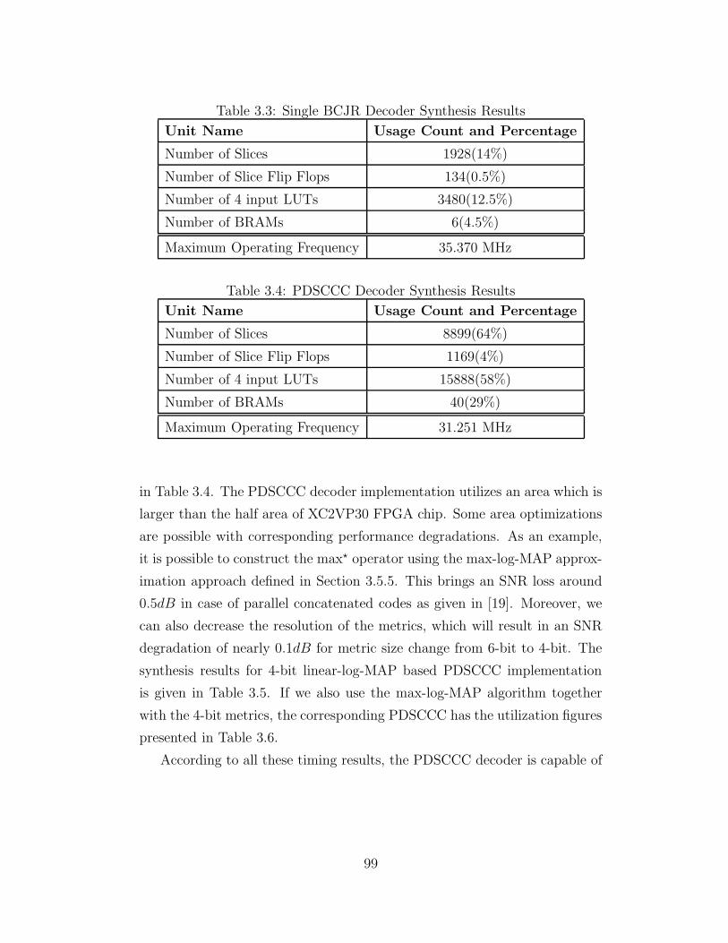
Table 3.3: Single BCJR Decoder Synthesis Results
Unit Name Usage Count and Percentage
Number of Slices 1928(14%)
Number of Slice Flip Flops 134(0.5%)
Number of 4 input LUTs 3480(12.5%)
Number of BRAMs 6(4.5%)
Maximum Operating Frequency 35.370 MHz
Table 3.4: PDSCCC Decoder Synthesis Results
Unit Name Usage Count and Percentage
Number of Slices 8899(64%)
Number of Slice Flip Flops 1169(4%)
Number of 4 input LUTs 15888(58%)
Number of BRAMs 40(29%)
Maximum Operating Frequency 31.251 MHz
in Table 3.4. The PDSCCC decoder implementation utilizes an area which is
larger than the half area of XC2VP30 FPGA chip. Some area optimizations
are possible with corresponding performance degradations. As an example,
it is possible to construct the max� operator using the max-log-MAP approx-
imation approach defined in Section 3.5.5. This brings an SNR loss around
0.5dB in case of parallel concatenated codes as given in [19]. Moreover, we
can also decrease the resolution of the metrics, which will result in an SNR
degradation of nearly 0.1dB for metric size change from 6-bit to 4-bit. The
synthesis results for 4-bit linear-log-MAP based PDSCCC implementation
is given in Table 3.5. If we also use the max-log-MAP algorithm together
with the 4-bit metrics, the corresponding PDSCCC has the utilization figures
presented in Table 3.6.
According to all these timing results, the PDSCCC decoder is capable of
99

Table 3.5: PDSCCC Decoder Synthesis Results(4-bit Metrics)
Unit Name Usage Count and Percentage
Number of Slices 6899(50%)
Number of Slice Flip Flops 961(3%)
Number of 4 input LUTs 12046(43%)
Number of BRAMs 28(20%)
Maximum Operating Frequency 33.649 MHz
Table 3.6: PDSCCC Decoder Synthesis Results(4-bit and Max-log-MAP)
Unit Name Usage Count and Percentage
Number of Slices 4159(30%)
Number of Slice Flip Flops 961(3%)
Number of 4 input LUTs 7355(26%)
Number of BRAMs 28(20%)
Maximum Operating Frequency 38.551 MHz
supplying a data throughput of 4.167 Mbps in the highest BER performance
case, that is for 6-bit metrics and linear-log-MAP. (Each iteration takes 120
cycles and for 8 iterations 128 uncoded data bits are decided at 31.255 clock
frequency.) For lower performance case given in Tables 3.5 and 3.6, the
throughputs are 4.487 Mbps and 5.140 Mbps respectively. These figure are
quite higher than some recent implementations of iterative approaches [20].
When the PDSCCC decoder is operated using the 24 Mhz clock source of
the other receiver modules, it still has a throughput of 3.2 Mbps.
3.7.2 Optimization and Implementation Issues
The PDSCCC decoder is a relatively huge hardware module especially when
the metric size is selected as 6 and linear-log-MAP algorithm is used. In
order to successfully implement and operate large designs some parameters
100

of Xilinx ISE should be set correctly. Firstly, within the Xilinx Constraints
Editor the clock signal should be defined and corresponding clock period
constraint must be set according to the operating frequency. In order to
assure that all calculation results are assigned to corresponding registers
correctly, the pad to setup constraint should be set as at most half the period
of the clock signal. This constraint guarantees that any input signal from the
outside world observes a combinational delay at most at the required length.
Similarly, the clock to pad constraint determines the maximum combinational
delay for a signal traveling from the output of a register to an output pad
and it is usually set as the half clock period as well. In addition to these,
some advanced implementation parameters should be tuned for expected
circuit behavior. These parameters are set from the properties dialog box
of the “Implement Design” phase. Map effort level is required to be set as
high and the optimization strategy as balanced between the area and speed
optimizations. Place and route effort level must also be set as high and
multi-pass place and route choice may be selected as well in order to avoid
placement and routing problems in large designs.
101

chapter 4
the papr problem in water-filling and a
suboptimal water-filling algorithm
The Chapters 2 and 3 are concentrated on implementation aspects of a com-
plete wireless communication testbed with all related RF transmission mod-
ules, signal processing blocks, and coding schemes used. This chapter, on
the other hand, is based on algorithms developed for signal transmission in
the next step of the testbed implementation with orthogonal frequency di-
vision multiplexing (OFDM) and multiple input multiple output (MIMO)
methods. Few key points have been described about the MIMO perspective
of the testbed development in Chapter 2. Also no details on the OFDM
implementation has been given since the fast Fourier transform (FFT) algo-
rithm (which is the basis for OFDM transmission) was under development
during the submission of this thesis. However, we carried out many simula-
tions and derived some analytical results for the possible algorithms that had
potential usage in the final MIMO-OFDM system. The essential goal of the
algorithms tested is decreasing a parameter, known as peak-to-average-power
ratio (PAPR), in MIMO-OFDM testbed transmitter output.
4.1 Definition of PAPR
The peak-to-average-power ratio (PAPR) for a stochastic discrete time pro-
cess x[n] is given as,
PAPR =maxn | x[n] |2Ex {| x[n] |2} (4.1)
102

According to the definition of PAPR, some simple examples can be given to
demonstrate the PAPR for some schemes. The PAPR of a system with PSK
modulated output symbols is trivially 1 due to constant amplitude at the
output. In opposition to the PSK modulation scheme, with square M-QAM
modulations (M>4), the PAPR is always greater than 1, since the peak power
is associated with the symbols on the corners that have larger magnitude then
the other symbols. Also with multicarrier transmission schemes, signals may
add up constructively at some time instances while adding up destructively
at other instances, which may lead to a large dynamic range for the output
signal power, so a high PAPR.
Most of the power amplifiers at the last stage of the wireless transmitter
modules have nonlinear input vs. output power characteristics. Some models
for this nonlinearity are suggested in [24, 25]. According to the solid state
amplifier (SSA) model, as an example, the power characteristics of an ampli-
fier (with smoothness factor of 1, and saturation level of 1 Watt) is given in
Figure 4.1. It is obvious that when we use the amplifier in the linear region
we can transmit the desired signal without any power change. However, close
to the saturation region there is considerable degradation in the transmitted
signal power. This may result in severe signal distortion ([28]) unless PAPR
of the transmitted signal is reduced or the transmitted signal power is re-
duced so that the peak power will also be close to the linear region, which
is known as backoff. Applying high backoff to the transmitted signal has a
disadvantage of using the power amplifier in its low-efficiency region for most
of the time.
In most cases simply defining and using the maximum PAPR value as a
system performance parameter is practically insignificant. Considering the
very low probability of having the maximum possible PAPR value, in most
systems the cumulative distribution function of the PAPR is the performance
criteria for transmitted signal. Figure 4.2 demonstrates a comparison of two
systems in terms of the PAPR distribution of their output signals. These two
systems are arbitrary, but with the corresponding given PAPR distributions.
103

0 0.5 1 1.5 2 2.5 30
0.1
0.2
0.3
0.4
0.5
0.6
0.7
0.8
0.9
1
Input Power, W
Out
put P
ower
, W
Nonlinear Power Characteristics of an SSA
LinearRegion
SaturationRegion
Figure 4.1: The linear and the saturation regions of the power amplifier are
clearly distinguishable.
Several conclusions can be drawn from Figure 4.2. Firstly, we can compare
two systems by setting a probability value of interest under which we assume
the probability of having corresponding PAPR0 value is negligible. Assuming
this limit is set at 10−4 for a specific application such that in one symbol out
of 10000, we observe a problem due to high signal level. Therefore, in order
to avoid such problems we can backoff the average signal power level by
the corresponding PAPR0 value. This value is nearly 9.5dB for the first
system whereas it is almost 11dB for the second. Hence the designer of
the second system should decrease its average power level by 1.5dB more
than the first system’s designer so that both systems can operate with same
level of degradation on the output signal. This power reduction will pose a
disadvantage to the designer of the second system due to decreased SNR and
104

−15 −10 −5 0 5 10 1510
−6
10−5
10−4
10−3
10−2
10−1
100
PAPR0, dB
Pr(P
APR
>PA
PR0)
PAPR Cumulative Distribution Functions for Two Signals
Output of System 1Output of System 2
Figure 4.2: System 1 has better PAPR distribution property with lower
probabilities of surpassing a given level of PAPR0 value.
hence the decreased available channel capacity. Secondly, we can compare
two systems’ probabilities of having a specific PAPR0 value. As an example,
the first system will have 10dB instantaneous PAPR with the probability of
4×10⁻⁵ and the second system with the probability of 5×10⁻⁴. If no backoff
is applied and the critical signal distortion level is set as PAPR0 = 10dB, the
second system will roughly have its symbols degraded with 10 times higher
probability than the first one.
4.2 PAPR Reduction Methods in Literature
Since PAPR is especially an intrinsic and crucial problem for multicarrier
systems, techniques for reducing PAPR are diversified with the increasing
105

interest in multicarrier systems in recent years. Although a detailed analysis
of all of the methods will not be given, some of the frequently used ones will
be named here [26].
� Amplitude Clipping and Filtering: This technique clips the sig-
nals over a given level to the desired output level. This clipping op-
eration usually generates some noise in the bandwidth of the signal
(in-band distortion) and also some noise out of the signal bandwidth
(out-of-band radiation). In order to suppress the out-of-band radiation
after clipping, filtering is applied to the signal which causes some addi-
tional PAPR problems. Thus, an iterative clipping and filtering stages
are suggested which result in excessive processing delays.
� Coding: This class of techniques is large with a lot of subclasses that
suggest reduction for distinct modulation schemes. One idea is to select
such codewords for transmission such that the overall combined effect of
the codewords results in decreased PAPR levels. This approach requires
large lookup tables and finding good codes that reduce PAPR. In [27],
for an OFDM system with MPSK modulation the optimum lengths
for Golay complementary codes are given. Using these sequences of
codes the PAPR level of the output signal is kept at desired levels
deterministically. In most cases, the coding for PAPR reduction suffers
from bandwidth efficiency loss due to very low coding rates.
� Selected Mapping: Preparing multiple versions of the data to be
transmitted, the one with the lowest PAPR value is selected in this
technique. As an example for an OFDM system, many FFT’s are ob-
tained for one data sequence and transmitter selects the optimum one
in terms of PAPR. Obviously this method is problematic when suffi-
ciently enough representations for the same signal is to be generated.
Hardware resources may be the bottleneck in implementation of se-
lected mapping technique.
106

4.3 PAPR Reduction in OFDM systems
Due to increased data rate requirements of modern applications the band-
width utilized for wireless communications has increased in the last decade.
The increased bandwidth usually comes with a problem to be remedied for
reliable communication. This problem is known as the intersymbol interfer-
ence and mainly caused by the selective response of the channel within the
communication bandwidth. To fight with this frequency selective response,
a method is to split the bandwidth utilized into subbands such that on each
subband the gain of the frequency selective channel is almost constant. Then
the data to be transmitted is also divided into substreams each of which has
only a fraction of the total data rate. Furthermore, the subcarrier frequencies
to carry these substreams are selected such that each modulated substream
is orthogonal to others in frequency domain. This type of modulation is
known as the orthogonal frequency division multiplexing (OFDM) and has
been used in many wideband wireless communication systems, such as IEEE
802.11a/g based wireless LANs, DVB terrestrial digital TV systems, IEEE
802.16 based WiMAX.
4.3.1 Definition of OFDM Signal
An OFDM signal can be defined as the time domain representation of the
data signal that is constructed in the frequency domain by assigning N sub-
streams of data to orthogonally spaced N subcarriers. This operation can
be implemented as an inverse fast Fourier transform (IFFT) operation [29].
The substreams may be modulated adaptively in the frequency domain be-
fore IFFT as shown in Figure 4.31. In order to mitigate the effects of multi-
path fading signal reception, a cyclic prefix is usually copied from the above
defined time domain signal’s end and attached to its head. This way the
synchronization mismatches are avoided, the orthogonality between the sub-
1Figure is taken from http://en.wikipedia.org/wiki/OFDM
107
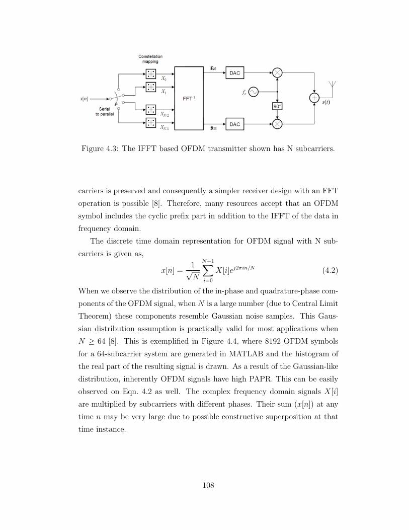
Figure 4.3: The IFFT based OFDM transmitter shown has N subcarriers.
carriers is preserved and consequently a simpler receiver design with an FFT
operation is possible [8]. Therefore, many resources accept that an OFDM
symbol includes the cyclic prefix part in addition to the IFFT of the data in
frequency domain.
The discrete time domain representation for OFDM signal with N sub-
carriers is given as,
x[n] =1√N
N−1∑i=0
X[i]ej2πin/N (4.2)
When we observe the distribution of the in-phase and quadrature-phase com-
ponents of the OFDM signal, when N is a large number (due to Central Limit
Theorem) these components resemble Gaussian noise samples. This Gaus-
sian distribution assumption is practically valid for most applications when
N ≥ 64 [8]. This is exemplified in Figure 4.4, where 8192 OFDM symbols
for a 64-subcarrier system are generated in MATLAB and the histogram of
the real part of the resulting signal is drawn. As a result of the Gaussian-like
distribution, inherently OFDM signals have high PAPR. This can be easily
observed on Eqn. 4.2 as well. The complex frequency domain signals X[i]
are multiplied by subcarriers with different phases. Their sum (x[n]) at any
time n may be very large due to possible constructive superposition at that
time instance.
108

−4 −3 −2 −1 0 1 2 3 40
1000
2000
3000
4000
5000
6000
7000
8000
9000
10000
Normalized Voltage
Number of Samples
Histogram of the Real Part of the 64−subcarrier OFDM signal
Figure 4.4: Gaussian characteristics of the histogram is obvious for real part
of the OFDM signal.
4.3.2 PAPR Problem with Optimal Power Allocation
in Frequency Domain
For time varying frequency selective channels, the optimal algorithm for
achieving channel capacity is the two-dimensional water-filling algorithm [8].
This algorithm allocates distinct power levels to each frequency at any time
according to the instantaneous SNR level of that frequency. The frequencies
with higher SNR levels receive higher power, while the worse frequencies ob-
tain less or no power according to a predefined threshold. A simple example
(using only one-dimensional water-filling in frequency domain at an instant)
for demonstrating the water-filling operation is given in Figure 4.5. The γ0
value shown in Figure 4.5 is the threshold, whose reciprocal will determine
109

−2.5 −2 −1.5 −1 −0.5 0 0.5 1 1.5 2 2.5
x 106
0
0.1
0.2
0.3
0.4
0.5
0.6
0.7
0.8
0.9
f , Hz
1/γ(f
)
The Inverse of SNR Function
P(f=1Mhz)Ptotal
1/γ0
Figure 4.5: The inverse of the SNR function is used for allocating the power
to frequencies.
the power to be allocated to various frequencies. The total power to be dis-
tributed is denoted by Ptotal and the power allocation, P (f, t), to frequency
f at time t is given as,
P (f, t)
Ptotal=
{1/γ0 − 1/γ(f, t) γ(f, t) ≥ γ0
0 γ(f, t) < γ0
. (4.3)
In Eqn. 4.3, γ(f, t) is used for the instantaneous SNR at frequency f at
time t. A very similar algorithm for optimally distributing a given power
to frequency-selective block fading channels can also be obtained. This al-
gorithm also applies to OFDM subcarrier power distribution, since within
the frequency subbands the frequency response of the channel is assumed to
follow block fading in frequency domain for OFDM. Figure 4.6 shows power
110
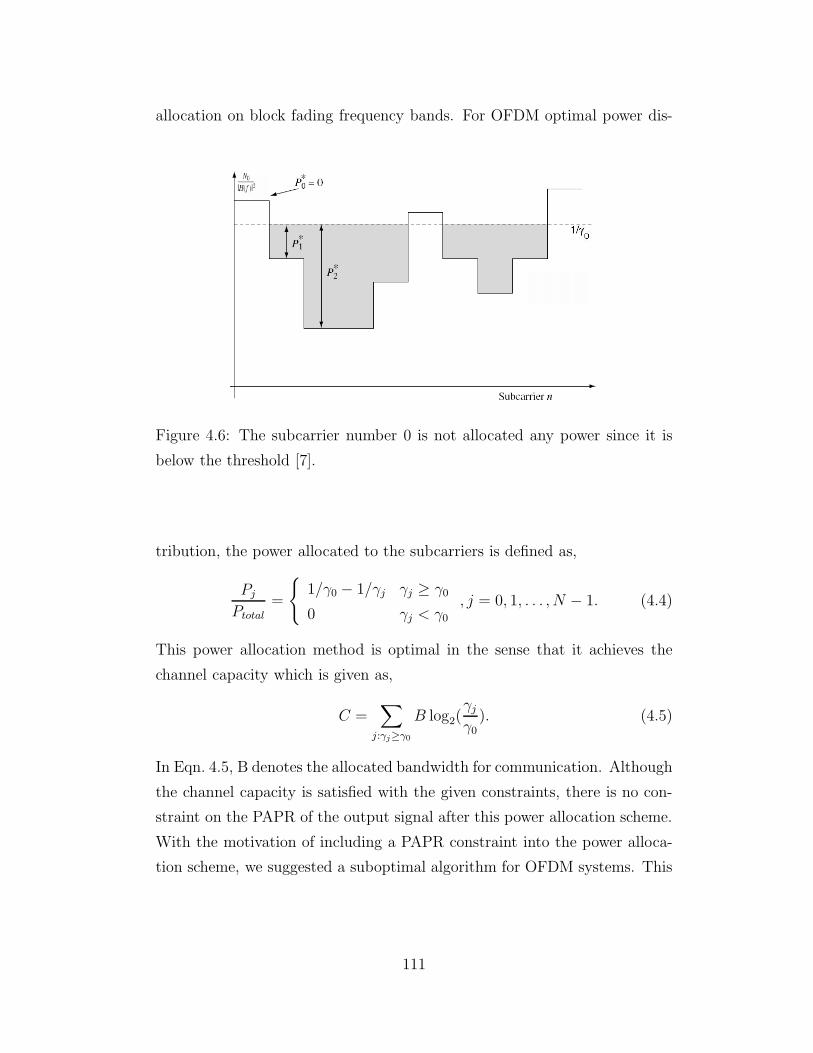
allocation on block fading frequency bands. For OFDM optimal power dis-
Figure 4.6: The subcarrier number 0 is not allocated any power since it is
below the threshold [7].
tribution, the power allocated to the subcarriers is defined as,
Pj
Ptotal
=
{1/γ0 − 1/γj γj ≥ γ0
0 γj < γ0
, j = 0, 1, . . . , N − 1. (4.4)
This power allocation method is optimal in the sense that it achieves the
channel capacity which is given as,
C =∑
j:γj≥γ0
B log2(γj
γ0). (4.5)
In Eqn. 4.5, B denotes the allocated bandwidth for communication. Although
the channel capacity is satisfied with the given constraints, there is no con-
straint on the PAPR of the output signal after this power allocation scheme.
With the motivation of including a PAPR constraint into the power alloca-
tion scheme, we suggested a suboptimal algorithm for OFDM systems. This
111

method is simple to apply when compared to the water-filling algorithm and
depends on distributing the given total power in equal amounts to a selected
number of subcarriers. The following section summarizes our analytical find-
ings on the PAPR of the OFDM signal when water-filling is utilized. It
further compares the optimal (water-filling) scheme and the scheme where
all the subcarriers are allocated equal power. Then, the next section com-
pares the suggested suboptimal scheme (allocating equal power to a selected
number of subcarriers) and the water-filling.
4.3.3 Comparison of Non-adaptive Scheme
with Water-filling
The cumulative probability distribution function of an OFDM signal with N
subcarriers is given in [8] as,
Fλ(λ) =Pr( maxi=0,1,...,N−1
| x[i] |2≤ λ), (4.6)
=(1 − e−λ)N . (4.7)
However, with two-dimensional water-filling at some instances most of the
SNR levels of the subcarriers may be lower than the threshold level. Then,
the power is saved for better channel SNR levels in future transmissions,
which will result in significantly varying PAPR for the power adapted OFDM
signal. Therefore, this requires a new analysis for determination of cu-
mulative probability distribution function with water-filling. In [30], the
instantaneous PAPR corresponding to an instantaneous SNR vector, γ =
{γ0, γ1, . . . , γN−1}, is found as,
Fλ(�γ)(λ(γ)) = (1 − e−λ/σ2�γ )N , (4.8)
112

where σ2�γ is the random variance of the channel SNR vector, γ. This random
variance is given as,
σ2�γ =E{ 1
N
N−1∑i=0
N−1∑j=0
√Pi(γi )
√Pj(γj )X[i]X�[j]ej2π(i−j)n/N}, (4.9)
=1
N
N−1∑i=0
Pi(γi). (4.10)
Then the cumulative probability distribution function for the PAPR is found
after taking expectation of the expression in Eqn. 4.8 over all realizations of
the channel SNR vector as,
Fλ(λ) =
∫· · ·
∫f�γ(γ0, . . . , γN−1)(1 − e−λ/σ2
�γ )Ndγ0 . . .dγN−1. (4.11)
For the following comparisons this analytical result is evaluated using the
Monte Carlo simulation method. Moreover, for all the water-filling and sub-
optimal method simulation results are obtained by generating 100000 channel
vectors with zero-mean Gaussian vector elements that have variance 1. The
channel capacity comparisons are carried out by generating 10000 channel
vectors for each average total SNR level.
Figure 4.7 presents the capacity of optimal power allocation algorithm
with the non-adaptive (suggested equal power allocation) algorithm. It is
easy to observe that water-filling algorithm degrades to equal power alloca-
tion method in the high SNR values. Around 10dB SNR value (at a capacity
of 2.5 bits/sec/Hz) the SNR loss due to equal power allocation is 2.5dB.
Around 0dB SNR the loss is approximately 5dB and around 30dB it is less
than 0.5dB. Figure 4.8 shows the PAPR performance of two methods at an
average SNR of 0dB. Moreover, it also demonstrates the analytical result
curve in a close proximity of the 2-D water-filling method’s curve. The SNR
loss due to the excess backoff should be done by the water-filling method is
slightly above 2dB at PAPR probability of 10−4.
Figures 4.9 and 4.10 show the comparison results for two methods at
average SNR levels 10dB and 30dB respectively. For 10dB average SNR,
113

0 5 10 15 20 25 300
0.5
1
1.5
2
2.5
3
3.5
Average SNR, dB
Cap
acity
(bi
ts p
er s
econ
d pe
r H
z)
Water−filling Capacity vs. Equal Power Allocation Capacity
Water−FillingEqual Power
Figure 4.7: Channel capacity of two methods are close for high SNR values.
4 6 8 10 12 1410
−6
10−5
10−4
10−3
10−2
10−1
100
λ0, dB
Pr(
λ>
λ0)
Complementary Cumulative Probability Distribution Functions at Average SNR = 0 dB
Analytical Result2−D Water−Filling SimulationEqual Power Allocation Simulation
Figure 4.8: The non-adaptive method offers better PAPR distribution.
114

4 6 8 10 12 1410
−6
10−5
10−4
10−3
10−2
10−1
100
λ0, dB
Pr(
λ>
λ0)
Complementary Cumulative Probability Distribution Functions at Average SNR = 10 dB
Analytical Result2−D Water−Filling SimulationEqual Power Allocation Simulation
Figure 4.9: The analytical PAPR result is in accordance with the simulated
water-filling PAPR curve.
the loss in water-filling algorithm is nearly 1dB, and for 30dB the PAPR
distributions of two methods are almost identical. As a result, the channel
capacity gain obtained by the optimal water-filling algorithm is not very high
when the nonlinear characteristics of power amplifiers, which are effected by
high PAPR values, is taken into account. The simple equal power allocation
method can perform with only 2.5 − 1 = 1.5dB performance degradation at
10dB average SNR. Furthermore, the analytical PAPR distribution suggested
by [30] strictly follows the simulation results at 10dB and higher SNR values.
This is mainly due to the fact that at very low SNR values the water-filling
method uses only a few subcarriers and they may not add up to Gaussian
distributed signals leading to invalidity of the Gaussian assumption in the
derivation.
115

4 6 8 10 12 14
10−4
10−3
10−2
10−1
100
λ0, dB
Pr(
λ>
λ0)
Complementary Cumulative Probability Distribution Functions at Average SNR = 30 dB
Analytical Result2−D Water−Filling SimulationEqual Power Allocation Simulation
Figure 4.10: Water-filling converges to equal power distribution.
4.3.4 Comparison of Subcarrier Selection
Scheme with Water-filling
In implementation of the power adaptation schemes, transmitter should be
fed back by the appropriate channel state information (like the SNR of each
subcarrier). The water-filling algorithm also requires information about the
power to be allocated to each subcarrier and this feedback may result in ex-
cessive utilization of the feedback channel. In order to reduce the time for
feedback, limited rate feedback may be preferred. In our scheme, instead of
sending the quantized subcarrier SNR values back to the transmitter, only
one bit per subcarrier is transmitted to reveal whether the corresponding sub-
carrier is allocated power or not. Therefore, the channel is used for shorter in-
tervals during each feedback event. This section presents the capacity curves
for various number of subcarriers (with highest SNR values) selected to carry
signal and it compares them with the optimal method. (In Appendices closed
116
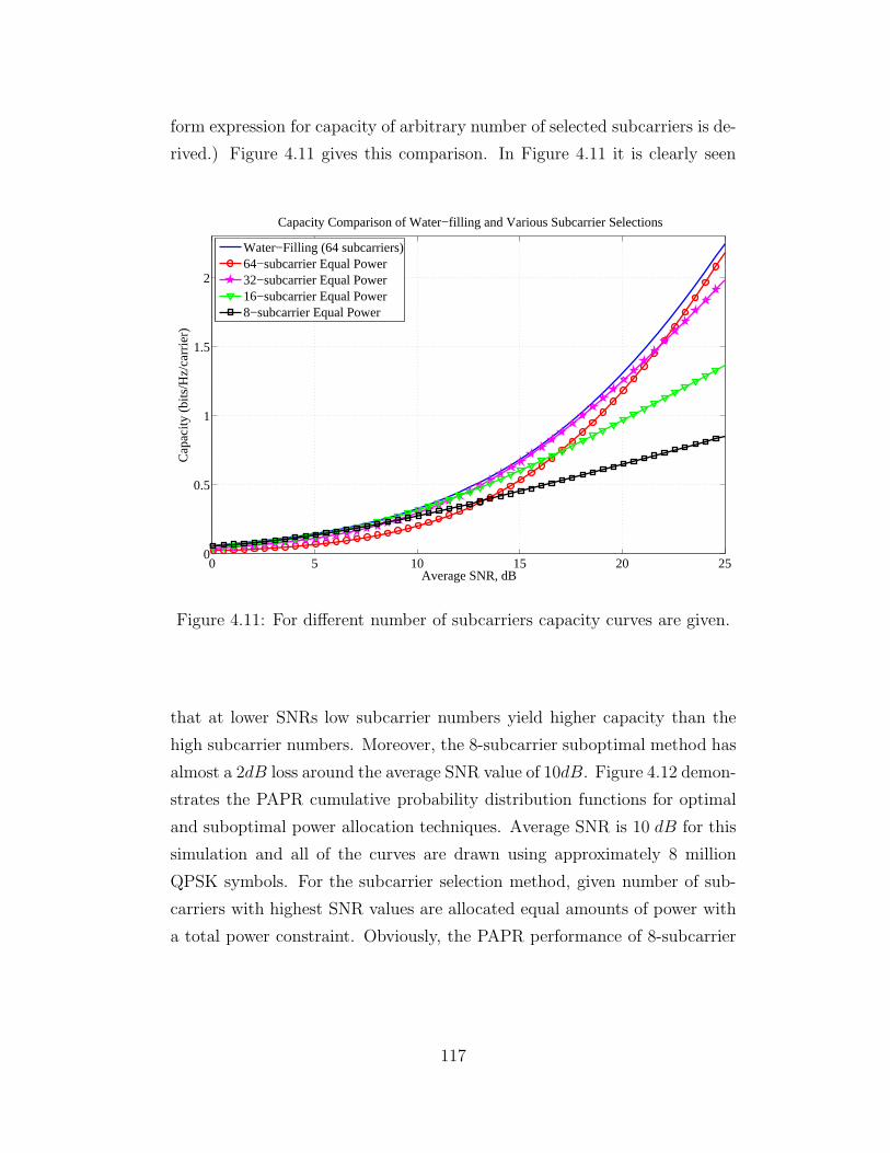
form expression for capacity of arbitrary number of selected subcarriers is de-
rived.) Figure 4.11 gives this comparison. In Figure 4.11 it is clearly seen
0 5 10 15 20 250
0.5
1
1.5
2
Average SNR, dB
Cap
acity
(bi
ts/H
z/ca
rrie
r)
Capacity Comparison of Water−filling and Various Subcarrier Selections
Water−Filling (64 subcarriers)64−subcarrier Equal Power32−subcarrier Equal Power16−subcarrier Equal Power8−subcarrier Equal Power
Figure 4.11: For different number of subcarriers capacity curves are given.
that at lower SNRs low subcarrier numbers yield higher capacity than the
high subcarrier numbers. Moreover, the 8-subcarrier suboptimal method has
almost a 2dB loss around the average SNR value of 10dB. Figure 4.12 demon-
strates the PAPR cumulative probability distribution functions for optimal
and suboptimal power allocation techniques. Average SNR is 10 dB for this
simulation and all of the curves are drawn using approximately 8 million
QPSK symbols. For the subcarrier selection method, given number of sub-
carriers with highest SNR values are allocated equal amounts of power with
a total power constraint. Obviously, the PAPR performance of 8-subcarrier
117
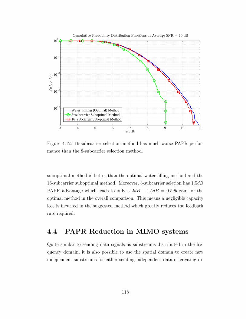
3 4 5 6 7 8 9 10 11
10−4
10−3
10−2
10−1
100
λ0, dB
Pr(
λ>
λ0)
Cumulative Probability Distribution Functions at Average SNR = 10 dB
Water−Filling (Optimal) Method8−subcarrier Suboptimal Method16−subcarrier Suboptimal Method
Figure 4.12: 16-subcarrier selection method has much worse PAPR perfor-
mance than the 8-subcarrier selection method.
suboptimal method is better than the optimal water-filling method and the
16-subcarrier suboptimal method. Moreover, 8-subcarrier seletion has 1.5dB
PAPR advantage which leads to only a 2dB − 1.5dB = 0.5db gain for the
optimal method in the overall comparison. This means a negligible capacity
loss is incurred in the suggested method which greatly reduces the feedback
rate required.
4.4 PAPR Reduction in MIMO systems
Quite similar to sending data signals as substreams distributed in the fre-
quency domain, it is also possible to use the spatial domain to create new
independent substreams for either sending independent data or creating di-
118

versity. Multiple-input multiple-output (MIMO) systems, in this sense, bare
resemblance to OFDM systems, with the distinction that the methods used
for achieving channel capacity differ. Consequently, it may be interesting to
analyze the PAPR properties of MIMO systems under different scenarios.
4.4.1 Overview of MIMO systems
Figure 4.13 shows the MIMO system in its most general form with Nt trans-
mit antennas and Nr receive antennas (called Nt×Nr MIMO system). Within
the MIMO wireless channel there are signal paths from all transmitter anten-
nas to all receiver antennas and for transmission various space-time coding
methods are possible. A MIMO wireless system is usually generalized by a
Figure 4.13: Many paths exist from the transmit antennas to the receive
antennas in a MIMO wireless channel.
matrix-vector equation that is given as,
y =
⎡⎢⎢⎣
y1
...
yNr
⎤⎥⎥⎦ = Hx+n =
⎡⎢⎢⎣
h11 . . . h1Nt
.... . .
...
hNr1 . . . hNrNt
⎤⎥⎥⎦⎡⎢⎢⎣
x1
...
xNt
⎤⎥⎥⎦+
⎡⎢⎢⎣
n1
...
nNr
⎤⎥⎥⎦ . (4.12)
119
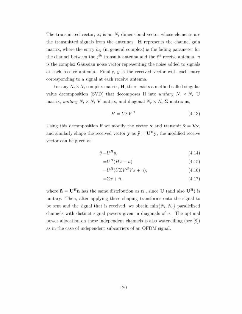
The transmitted vector, x, is an Nt dimensional vector whose elements are
the transmitted signals from the antennas. H represents the channel gain
matrix, where the entry hij (in general complex) is the fading parameter for
the channel between the jth transmit antenna and the ith receive antenna. n
is the complex Gaussian noise vector representing the noise added to signals
at each receive antenna. Finally, y is the received vector with each entry
corresponding to a signal at each receive antenna.
For any Nr×Nt complex matrix, H, there exists a method called singular
value decomposition (SVD) that decomposes H into unitary Nr × Nr U
matrix, unitary Nt × Nt V matrix, and diagonal Nr × Nt Σ matrix as,
H = UΣV H (4.13)
Using this decomposition if we modify the vector x and transmit x = Vx,
and similarly shape the received vector y as y = UHy, the modified receive
vector can be given as,
y =UHy, (4.14)
=UH(Hx + n), (4.15)
=UH(UΣV HV x + n), (4.16)
=Σx + n, (4.17)
where n = UHn has the same distribution as n , since U (and also UH) is
unitary. Then, after applying these shaping transforms onto the signal to
be sent and the signal that is received, we obtain min{Nt, Nr} parallelized
channels with distinct signal powers given in diagonals of σ. The optimal
power allocation on these independent channels is also water-filling (see [8])
as in the case of independent subcarriers of an OFDM signal.
120
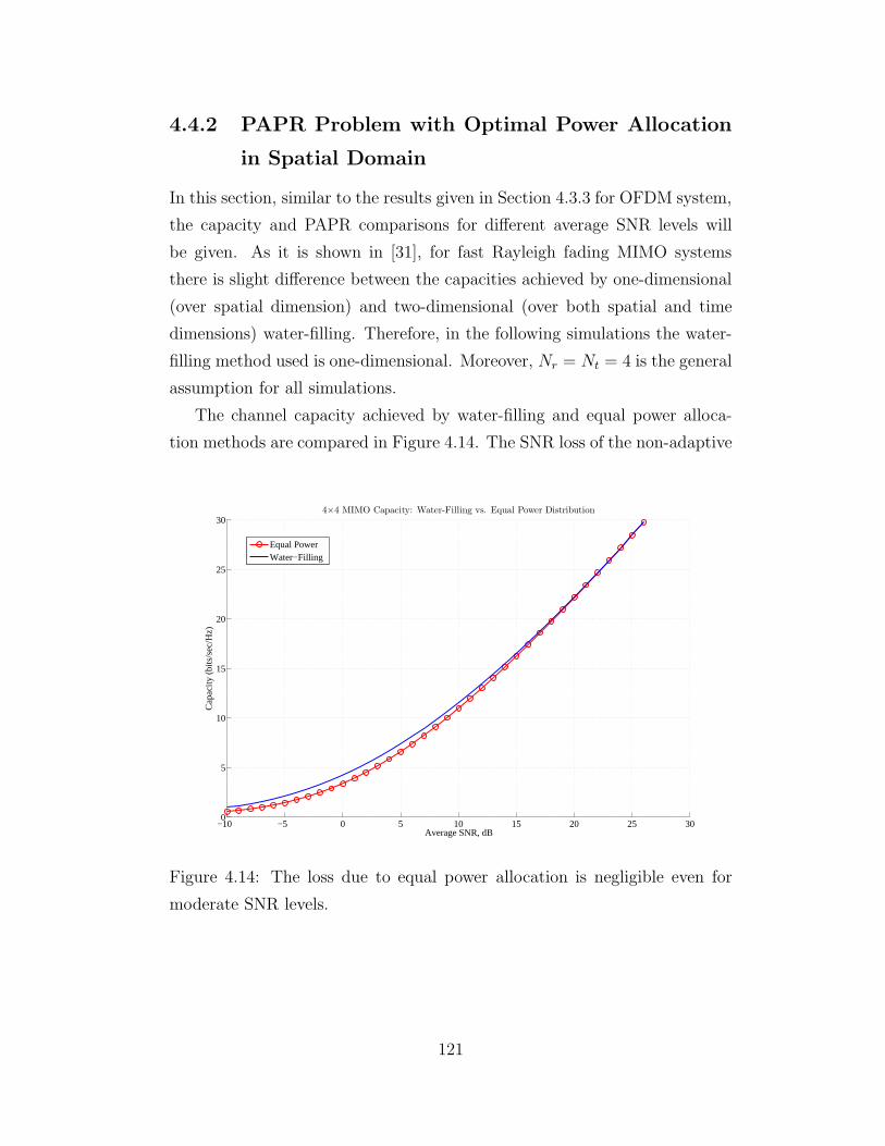
4.4.2 PAPR Problem with Optimal Power Allocation
in Spatial Domain
In this section, similar to the results given in Section 4.3.3 for OFDM system,
the capacity and PAPR comparisons for different average SNR levels will
be given. As it is shown in [31], for fast Rayleigh fading MIMO systems
there is slight difference between the capacities achieved by one-dimensional
(over spatial dimension) and two-dimensional (over both spatial and time
dimensions) water-filling. Therefore, in the following simulations the water-
filling method used is one-dimensional. Moreover, Nr = Nt = 4 is the general
assumption for all simulations.
The channel capacity achieved by water-filling and equal power alloca-
tion methods are compared in Figure 4.14. The SNR loss of the non-adaptive
−10 −5 0 5 10 15 20 25 300
5
10
15
20
25
30
Average SNR, dB
Cap
acity
(bi
ts/s
ec/H
z)
4×4 MIMO Capacity: Water-Filling vs. Equal Power Distribution
Equal PowerWater−Filling
Figure 4.14: The loss due to equal power allocation is negligible even for
moderate SNR levels.
121

method is close to 2dB around 0dB average SNR, 0.5dB around 10dB average
SNR, and negligibly small around 25dB average SNR. Figure 4.15 demon-
strates the PAPR distributions for two methods at 0dB average SNR. For
−10 −5 0 5 10 1510
−6
10−5
10−4
10−3
10−2
10−1
100
λ0, dB
Pr(
λ>
λ0)
Cumulative Probability Distribution Functions at Average SNR = 0 dB
Water−FillingEqual Power
Figure 4.15: Equal power allocation is much less prone to PAPR problems.
0dB average SNR and a fixed PAPR probability of 10−4, the extra backoff
for the water-filling power allocation method is almost 1.5dB when com-
pared with the equal power allocation method. Hence the overall gain for
the optimal method is close to a meager 0.5dB. Figure 4.16 is drawn for
10dB average SNR. When we set the PAPR probability at 10−4, the loss of
the water-filling method is nearly 0.5dB, which makes it comparable with
the non-adaptive method in terms of channel capacity. Finally, Figure 4.17
shows us that two methods converge to each other when the average SNR is
25dB.
122

−10 −5 0 5 10
10−4
10−3
10−2
10−1
100
λ0, dB
Pr(
λ>
λ0)
Cumulative Probability Distribution Functions at Average SNR = 10 dB
Water−FillingEqual Power
Figure 4.16: An observable PAPR performance difference still exists between
two methods.
−10 −5 0 5 10
10−4
10−3
10−2
10−1
100
λ0, dB
Pr(
λ>
λ0)
Cumulative Probability Distribution Functions at Average SNR = 25 dB
Water−FillingEqual Power
Figure 4.17: PAPR problem effects two systems almost identically.
123
chapter 5
conclusions and future work
There are three main themes of this thesis:
� The SISO and SIMO wireless testbed structures are described, cor-
responding filtering operations and the symbol detection results are
discussed. The maximal ratio combining method applied on the SIMO
system is shown to achieve much better bit error rates than the SISO
system, which encourages further studies with the MIMO approach.
� A parallelized serially concatenated convolutional code structure is de-
fined and its fixed point implementation based on the linear-log-MAP
algorithm is detailed. Various parameters effective on the performance
of the corresponding decoder are presented and final data throughput
for each major case is listed.
� The effect of optimal power allocation technique for OFDM and MIMO
systems on the PAPR of the output signal are investigated. The re-
sults for the comparison of this algorithm with the simplest equal power
allocation technique are given and the gain obtained by using the opti-
mal technique is shown to be small for especially 4× 4 MIMO system.
Moreover, a closed form expression for the capacity of a suboptimal
subcarrier selection method is derived (see Appendices).
In addition to the achievements described in this thesis, some improve-
ments to our testbed are set as future goals. These goals can be itemized as
follows:
124

� In order to optimize the system performance, the frequency modulating
(FM) RF transmitter/receiver modules described in Section 2.2.4 have
to be replaced with new transciever modules using amplitude modu-
lation (AM). This replacement has forced us to design a new board
that uses the desired modulation and supports up to 4 receive and 4
transmit antennas. The new testbed is also expected to operate FFT
modules for realizing OFDM. Moreover, the optimal adaptive power
allocation methods and their suboptimal counterparts for both MIMO
and OFDM can also be experimented on this second version of the
testbed.
� For further improving the data throughput of the iterative decoder ar-
chitecture discussed in Section 3.5, the number of the parallel decoders
in the inner and/or the outer decoder can be increased. Moreover,
some pipelining stages may be inserted into metric and log-likelihood
calculations in order to improve the operating clock frequency.
� The serial port connection of the FPGA board with the computer may
be upgraded to support USB. This may decrease the data acquisition
time and provide real-time data acquisition for an in-depth analysis of
the wireless channel properties .
� Rate adaptation over various spatial or frequency dimensions may be
implemented with the addition of higher rate modulation schemes to
the current QPSK modulation.
In addition to equal power allocation method for MIMO and OFDM sys-
tems, we analyzed the achievable capacity for suboptimal algorithms utilized
during the distribution of the power over antennas and/or subcarriers. We
mainly concentrated on selection of a predetermined number of the possible
antennas and allocating the power in equal amounts to these antennas in
MIMO systems. The capacity obtained by such a method requires analyzing
the random eigenvalue distributions for the channel response matrix. After
125

some detailed derivations that include second order integral approximations
for the capacity expressions we could not manage to obtain a convenient so-
lution to the problem due to mathematical intricacies involved. This is also
a problem that remains to be solved in near future.
The observation of PAPR and capacity comparisons under more realistic
conditions may also be an interesting extension to the problems described
here. The correlation of the subcarriers in the OFDM system and the cor-
relation of the receive antennas in the MIMO system would be nice starting
points. The bit error rate performance of the competing methods, with all
the coding and modulation schemes included as the system parameters, may
also be investigated. Furthermore, realistic nonlinear power amplifier models
may also be added in this comparisons.
126

appendices
Analytical Capacity of Suboptimal Water-
Filling Algorithm for OFDM
The instantaneous capacity for a Rayleigh Fading channel is given as,
C = B log2(1 + γ), (A-1)
where γ is the instantaneous SNR value and B is the bandwidth of the
channel. The distribution of γ is exponential and given as,
fγ(γ) =
(1
γ0
)e− γ
γ0 , (A-2)
where γ0 is the expected value of γ. Then the expected channel capacity for
a Rayleigh fading channel is given as,
Eγ [C] =
∫ ∞
0
B log2(1 + γ)fγ(γ)dγ, (A-3)
=B
ln 2
∫ ∞
0
ln(1 + γ)(1
γ0)e
− γγ0 dγ, (A-4)
=B
ln 2e1/γ0E1(1/γ0). (A-5)
In Eqn. A-5, E1(x) is the En function (with n = 1) whose definition is given
as,
En(x) ≡∫ ∞
1
1
γne−xγdγ. (A-6)
For obtaining the capacity of a number of selected independent subcarriers’
total capacity the following properties will be utilized:
� Property-1:∫ ∞
0
ln(1 + γ)(1
γ0)e
− kγγ0 dγ =
ek/γ0
kE1
(k
γ0
). (A-7)
127

� Property-2: For n independently distributed random variables, the
probability distribution function of the ith smallest variable for ordered
statistics is given as,
fγ(i)(γ) =
n!
(i − 1)! · (n − i)!(Fγ(γ))i−1(1 − Fγ(γ))n−ifγ(γ), (A-8)
=i ·(
n
i
)(Fγ(γ))i−1(1 − Fγ(γ))n−ifγ(γ). (A-9)
Problem-1: What is the capacity when always the best channel (that is
γ(n)) is allocated the whole power?
Solution: Using Property-2, the expected value for the capacity of the high-
est SNR channel is given as,
E[log2(1 + γ(n))] =B
ln 2
∫ ∞
0
ln(1 + γ)n!
(n − 1)!0!(1 − e
− γγ0 )n−1
(1
γ0
)e− γ
γ0 dγ,
(A-10)
=B
ln 2
∫ ∞
0
ln(1 + γ)n!
(n − 1)! · 0!
.
(n−1∑j=0
(n − 1
j
)(−1)je
− jγγ0
)(1
γ0
)e− γ
γ0 dγ, (A-11)
=B
ln 2n
n−1∑j=0
(n − 1
j
)(−1)j
∫ ∞
0
ln(1 + γ)
.
(1
γ0
)e− (1+j)γ
γ0 dγ. (A-12)
Now, if we apply the Property-1 on Eqn. A-12, the capacity is given as,
E[log2(1+γ(n))] =B
ln 2n
n−1∑j=0
(n − 1
j
)(−1)j 1
1 + je
1+jγ0 E1
(1 + j
γ0
). (A-13)
Problem-2: What is the capacity when the k best channels among n inde-
pendent Rayleigh channels are allocated equal power?
Solution: We need to find E[log 2(1 + γ(t))] for t = n − k + 1, . . . , n and
128

sum the results for the total capacity. The capacity of an individual channel
can be obtained using the Properties-1 and 2 as,
E[log2(1 + γ(t))] =B
ln 2
∫ ∞
0
ln(1 + γ)t
(n
t
)(1 − e
− γγ0 )t−1
.(e− γ
γ0 )n−t
(1
γ0
)e− γ
γ0 dγ, (A-14)
=B
ln 2
∫ ∞
0
ln(1 + γ)t
(n
t
)(t−1∑j=0
(t − 1
j
)(−1)je
− jγγ0
)
.(e− γ
γ0 )n−t
(1
γ0
)e− γ
γ0 dγ, (A-15)
=B
ln 2t
(n
t
)t−1∑j=0
(t − 1
j
)(−1)j
∫ ∞
0
ln(1 + γ)e− jγ
γ0
.e− (n−t)γ
γ0
(1
γ0
)(e
− γγ0 )n−tdγ, (A-16)
=B
ln 2t
(n
t
)t−1∑j=0
(t − 1
j
)(−1)j 1
j + n − t + 1
.ej+n−t+1
γ0 E1
(j + n − t + 1
γ0
). (A-17)
Finally, using Eqn. A-17, the capacity for suboptimal subcarrier selection
method can be found as,
E
[n∑
t=n−k+1
log2(1 + γ(t))
]=
n∑t=n−k+1
E[log2(1 + γ(t))]. (A-18)
129

references
[1] Emre Telatar, “Capacity of multi-antenna Gaussian channels”, Europ.
Trans. Commun., vol. 10, no. 6, pp. 585–595, 1999.
[2] Austin Lesea, Saar Drimer, “That is So Random!”, Xilinx TechXclusives
Articles, June 2004
[3] John G. Proakis, “Digital Communications”, McGraw-Hill Science En-
gineering Aug. 2000,
[4] L. R. Bahl, J. Cocke, F. Jelinek, and J.Raviv, “Optimal decoding of
linear codes for minimizing symbol error rate” IEEE Transactions on
Information Theory, vol. IT-20, pp.284-287, Mar. 1974
[5] R. A. Scholtz, “Frame synchronization techniques”, IEEE Trans. Com-
mun., vol. COM-28, pp. 1204-1213, 1980.
[6] U. Meyer-Baese, “Digital Signal Processing with Field Programmable
Gate Arrays”, Springer, 2004.
[7] David Tse, Pramod Viswanath, “Fundamentals of Wireless Communi-
cation”, Cambridge University Press, 2005.
[8] Andrea Goldsmith, “Wireless Communications”, Cambridge University
Press, 2005.
[9] Alexander Barg, Gilles Zmor, “Concatenated Codes: Serial and Par-
allel”, IEEE Transactions on Information Theory, vol. 51, no. 5, May
2005
[10] Orhan Gazi, “Parallelized Architectures for Low Latency Turbo Struc-
tures”, PhD. Dissertation submitted to Graduate School of Natural and
Applied Sciences of Middle East Technical University, Jan. 2007
130

[11] Stephan B. Wicker, “Error Control Systems for Digital Communication
and Storage”, Prentice-Hall, Jan. 1995.
[12] S. Lin, D. J. Costello Jr, “Error Control Coding: Fundamentals and
Applications”, Prentice-Hall, 1983.
[13] B. J. Frey and D. J. C. MacKay, “Performance of Parallel and Serial
Concatenated Codes on Fading Channels” IEEE TRANSACTIONS ON
COMMUNICATIONS, vol. 50, vo. 10, OCTOBER 2002Vucetic
[14] S. Benedetto, G. Montorsi, D. Divsalar, and F. Pollara, “Serial concate-
nation of interleaved codes: performance analysis, design and iterative
decoding”, Transactions on Information Theory, vol. 44, no. 3, MAY
1998
[15] J. Hagenauer, P. Hoeher, “Concatenated Viterbi decoding,” in Proc. 4th
Joint Swedish-Soviet Int. Workshop on Information Theory, pp. 2933,
Aug. 1989.
[16] G. D. Forney, Jr., “Concatenated Codes. Cambridge”, MA: MIT Press,
1966.
[17] C. Berrou, A. Glavieux, P. Thitimajshima, “Near Shannon limit
error-correcting coding and decoding: Turbo-codes”,Proc. ICC93, pp.
10641070, May 1993.
[18] S. Dolinar, D. Divsalar, “Weight Distribution for Turbo codes Using
Random and Nonrandom Permutations”,JPL Progress Report 42-122
pp. 56-65, Aug. 1995.
[19] M.C. Valenti and J. Sun, “The UMTS turbo code and an efficient de-
coder implementation suitable for software defined radios”, Int. J. Wire-
less Info. Networks, vol. 8, no. 4, pp. 203-216, Oct. 2001.
131

[20] Mike Cheng, Mike Nakashima, Jon Hamkins, Bruce Moision, and Maged
Barsoum, “A Decoder Architecture for High-Speed Free Space Laser
Communications” , Proceedings of SPIE,Volume 5712, Free-Space Laser
Communication Technologies XVII, Apr. 2005.
[21] Y. Wu, B. Woerner, “The influence of quantization and fixed point arith-
metic upon the BER performance of turbo codes”, in Proc IEEE VTC
1999, pp. 16831687, May 1999.
[22] T. A. Summers, S. G. Wilson, “SNR Mismatch and Online Estimation
in Turbo Decoding”, IEEE Transactions on Communications, vol. 46,
no.4, pp. 421423, Apr. 1998.
[23] A. Worm, P. Hoeher, N. When, “Turbo-decoding without SNR estima-
tion”, IEEE Commun. Lett., vol. 4, pp. 193-195, June 2000.
[24] Elena Costa, Michele Midrio, Silvano Pupolin, “Impact of Nonlinearities
on OFDM Transmission System Performance”, IEEE Commun. Lett.,
vol. 3, no. 2, Feb 1999.
[25] Tim C.W. Schenk, Peter F.M. Smulders, Erik R. Fledderus, “Impact
of nonlinearities in multiple-antenna OFDM transceivers”, Communica-
tions and Vehicular Technology, 2006 Symposium on , pp.53-56, 23-23
Nov. 2006.
[26] Seung Hee Han, Jae Hong Lee, “An overview of peak-to-average power
ratio reduction techniques for multicarrier transmission”, Wireless Com-
munications, IEEE Volume 12, Issue 2, Apr. 2005.
[27] T. Hunziker, U.P. Bernhard, “Evaluation of Coding and Modulation
Schemes based on Golay Complementary Sequences for Efficient OFDM
Transmission”, Vehicular Technology Conference, 1998. VTC 98. 48th
IEEE, vol. 2, May 1998.
132
[28] Chris van den Bos, Michiel H.L. Kouwenhoven, C.J.M. Verhoeven,
“Non-linear Distortion and OFDM Bit Error Rate”, Proc. ProRISC
CSSP, Nov. 1999.
[29] Henrik Schulze, Christian Luders, “Theory and Applications of OFDM
and CDMA”, John Wiley & Sons, 2005.
[30] Mehmet Vural, Tugcan Aktas, Ali Ozgur Yilmaz, “Effect of Water-
Filling Method on the PAPR for OFDM and MIMO Systems”, Sinyal
Isleme ve Iletisim Uygulamalari Kurultayı, June 2007.
[31] Zukang Shen, R.W. Heath Jr., J.G. Andrews, B.L. Evans, “Comparison
of space-time water-filling and spatial water-filling for MIMO fading
channels”, GLOBECOM 2004 IEEE, vol. 1, Nov. 2004.
[32] Weidong Xiang, Paul Richardson, Brett Walkenhorst, Xudong Wang,
Thomas Pratt, “A High-Speed Four-Transmitter Four-Receiver MIMO
OFDM Testbed: Experimental Results and Analyses”, EURASIP JASP,
Special Issue on MIMO Testbed, vol. 2006, no. 4, pp. 1-10.
133