Embed Size (px)
Citation preview

Multi-Gigabit/s/channel Parallel Optical Data Link Design in CMOS
Technology
by
Bindu Madhavan
A Dissertation Presented to the
FACULTY OF THE GRADUATE SCHOOL
UNIVERSITY OF SOUTHERN CALIFORNIA
In Partial Fulfillment of the
Requirements for the Degree
DOCTOR OF PHILOSOPHY
(ELECTRICAL ENGINEERING -- SYSTEMS)
August 2000
Copyright 2000 Bindu Madhavan

ii
Dedication
To My Parents

iii
Acknowledgments
I am deeply indebted to my advisor, Anthony Levi for his guidance and support. He
has been the ideal advisor in providing the environment and the facilities that have made
this work possible. His demand for excellence, insight, and suggestions have shaped many
of my ideas, and made this dissertation possible. His expertise in bonding ICs has been a
significant factor in achieving the data rates in this work. I also thank the members of my
dissertation and qualifying exam committees for their help and comments: Al Despain, a
wonderful committee chairperson and a rare Renaissance person, Daniel Dapkus, Timothy
Mark Pinkston, and John Choma.
This work has been done under the aegis of the POLO and PONI projects with the
POLO/PONI team at Agilent Technologies under Dave Dolfi. I would like to thank Lisa
Buckman, Kirk S. Giboney, and Joe Straznicky at Agilent Technologies for various
discussions. Working in the POLO and PONI projects at the Advanced Interconnect
Network Technology laboratory at USC has been an exciting learning experience because
of my interactions with Barton Sano, Yong-Seon Koh, Bharath Raghavan, Tsu-Yau
Chuang, Young-Gook Kim, Ashok Kanjamala, Sumesh Mani Thiyagarajan and Panduka
Wijetunga. David Cohen deserves special mention because of his unfailing courtesy and
readiness to answer questions, least of which involved Microsoft software and PCs. I owe
many thanks to Jen-I Pi (now at Zilog) for many discussions on semiconductor device
technology. I owe special thanks to Jeff Sondeen, for various discussions over the years on
CAD related issues, especially those pertaining to the layout tool magic, and for helping
out with many PERL scripts, which made life so much easier during the transformer
modeling and noise simulations of the opto-electronic receiver array. This dissertation has
benefited greatly from the careful reading of its many drafts by Ganapathy Parthasarathy

iv
and Jeff Sondeen. Apoorv Srivastava’s assistance in providing the thesis template in
FrameMaker and his willingness to answer questions is gratefully acknowledged. Kim
Reid deserves special mention for her wonderful role as the administrative assistant of the
laboratory. Sam Reynolds, Joel Goldberg and Wes Hansford, all at MOSIS, deserve
special mention for easing the path of the fabrication of 28 ICs that were fabricated as part
of this work.
It goes without saying that none of this would have been possible without the unfailing
support of my family.
This research was supported partially by the Defense Advanced Research Projects
Agency through the POLO and PONI projects with Agilent Technologies through
research grants.

v
Table Of Contents
Dedication . . . . . . . . . . . . . . . . . . . . . . . . . . . . . . . . . . . . . . . . . . . . . . . . . . . . . . . . . . ii
Acknowledgments . . . . . . . . . . . . . . . . . . . . . . . . . . . . . . . . . . . . . . . . . . . . . . . . . . iii
List of Figures . . . . . . . . . . . . . . . . . . . . . . . . . . . . . . . . . . . . . . . . . . . . . . . . . . . . . . ix
List of Tables . . . . . . . . . . . . . . . . . . . . . . . . . . . . . . . . . . . . . . . . . . . . . . . . . . . . . xxv
Table of constants and values . . . . . . . . . . . . . . . . . . . . . . . . . . . . . . . . . . . . . . . xxvii
List of Symbols . . . . . . . . . . . . . . . . . . . . . . . . . . . . . . . . . . . . . . . . . . . . . . . . . . xxviii
List of Abbreviations and Acronyms . . . . . . . . . . . . . . . . . . . . . . . . . . . . . . . . . xxxi
Abstract . . . . . . . . . . . . . . . . . . . . . . . . . . . . . . . . . . . . . . . . . . . . . . . . . . . . . . . . . xxxv
Chapter 1 Introduction 1
1.1 Motivation . . . . . . . . . . . . . . . . . . . . . . . . . . . . . . . . . . 11.2 Electrical Interconnect Loss . . . . . . . . . . . . . . . . . . . . . . . . . 71.3 Parallel Optical Interconnect . . . . . . . . . . . . . . . . . . . . . . . .121.4 CMOS Multi-Gb/s/pin Parallel Data Link Design . . . . . . . . . . . . .261.5 Dissertation Question . . . . . . . . . . . . . . . . . . . . . . . . . . . .281.6 Hypothesis . . . . . . . . . . . . . . . . . . . . . . . . . . . . . . . . . .281.7 Dissertation Contributions . . . . . . . . . . . . . . . . . . . . . . . . . .301.8 Dissertation Outline . . . . . . . . . . . . . . . . . . . . . . . . . . . . .301.9 A Note on Style . . . . . . . . . . . . . . . . . . . . . . . . . . . . . . .341.10 Summary. . . . . . . . . . . . . . . . . . . . . . . . . . . . . . . . . . .34
Chapter 2 Related Work 35
2.1 Parallel Data Links. . . . . . . . . . . . . . . . . . . . . . . . . . . . . .372.2 Receiver Design . . . . . . . . . . . . . . . . . . . . . . . . . . . . . . .372.3 Transmitter Design . . . . . . . . . . . . . . . . . . . . . . . . . . . . .432.4 Summary. . . . . . . . . . . . . . . . . . . . . . . . . . . . . . . . . . .46
Chapter 3 Parallel Data Link Components 47
3.1 Parallel Data Link Design Approach . . . . . . . . . . . . . . . . . . . .47

vi
3.2 Parallel Data Link Example . . . . . . . . . . . . . . . . . . . . . . . . .493.3 Load Impedance . . . . . . . . . . . . . . . . . . . . . . . . . . . . . . .573.4 Flip-Flop Circuit . . . . . . . . . . . . . . . . . . . . . . . . . . . . . . .643.5 Divider Circuits . . . . . . . . . . . . . . . . . . . . . . . . . . . . . . .69
3.5.1 Prescaler Design . . . . . . . . . . . . . . . . . . . . . . . . . . . .753.5.2 High-Speed Differential Logic Gates . . . . . . . . . . . . . . . . .823.5.3 Prescaler measurements . . . . . . . . . . . . . . . . . . . . . . . .863.5.4 Toggle Flip-Flops with RESET . . . . . . . . . . . . . . . . . . . .92
3.6 Slow-speed Logic Circuitry . . . . . . . . . . . . . . . . . . . . . . . . .943.7 Clock Distribution . . . . . . . . . . . . . . . . . . . . . . . . . . . . . .97
3.7.1 The Design of the Clock Distribution Circuit . . . . . . . . . . . . .983.7.2 System Level Advantages of Proposed Approach. . . . . . . . . . .993.7.3 Layout Considerations . . . . . . . . . . . . . . . . . . . . . . . . 1003.7.4 Simulation and Measurement Results . . . . . . . . . . . . . . . . 1013.7.5 Sources of Skew . . . . . . . . . . . . . . . . . . . . . . . . . . . 1033.7.6 Scalability to Significantly Larger Systems . . . . . . . . . . . . . 1043.7.7 Disadvantages of the Clock Distribution Scheme . . . . . . . . . . 1053.7.8 Low Output-Impedance Clock Driver . . . . . . . . . . . . . . . . 105
3.8 Electrical Receiver Circuit. . . . . . . . . . . . . . . . . . . . . . . . . 1103.9 PECL/ECL Transmit (Tx) Circuit . . . . . . . . . . . . . . . . . . . . . 1123.10 LVDS Transmit (Tx) Circuit . . . . . . . . . . . . . . . . . . . . . . . 1143.11 0.5 µm CMOS LVDS Rx-Tx Measurements . . . . . . . . . . . . . . . 1183.12 Summary. . . . . . . . . . . . . . . . . . . . . . . . . . . . . . . . . . 122
Chapter 4 PLL based Frequency Synthesizer Design 124
4.1 Phase Locked Loops: . . . . . . . . . . . . . . . . . . . . . . . . . . . 1264.2 VCO Design . . . . . . . . . . . . . . . . . . . . . . . . . . . . . . . . 129
4.2.1 Ring Oscillator Design. . . . . . . . . . . . . . . . . . . . . . . . 1334.2.2 VCO Control Stage Design . . . . . . . . . . . . . . . . . . . . . 1434.2.3 Jitter Sources in Ring Oscillators: . . . . . . . . . . . . . . . . . . 1544.2.4 VCO Measurements . . . . . . . . . . . . . . . . . . . . . . . . . 1584.2.5 VCO Design Summary . . . . . . . . . . . . . . . . . . . . . . . 178
4.3 Phase Frequency Detector . . . . . . . . . . . . . . . . . . . . . . . . . 1804.3.1 Digital Phase Frequency Detector . . . . . . . . . . . . . . . . . . 1804.3.2 XOR Based PFD. . . . . . . . . . . . . . . . . . . . . . . . . . . 186
4.4 Loop-filter . . . . . . . . . . . . . . . . . . . . . . . . . . . . . . . . . 1904.5 Noise Control Mechanisms . . . . . . . . . . . . . . . . . . . . . . . . 196
4.5.1 Noise Reduction Techniques . . . . . . . . . . . . . . . . . . . . 1974.5.2 Static-Phase Error . . . . . . . . . . . . . . . . . . . . . . . . . . 1994.5.3 Spurious Modulation. . . . . . . . . . . . . . . . . . . . . . . . . 2004.5.4 Choosing K . . . . . . . . . . . . . . . . . . . . . . . . . . . . . 201
4.6 PLLFS IC Measurements . . . . . . . . . . . . . . . . . . . . . . . . . 201

vii
4.7 Summary . . . . . . . . . . . . . . . . . . . . . . . . . . . . . . . . . 210
Chapter 5 Mux/Demux Array Design 212
5.1 Broadband 1:N Demultiplexer and N:1 Multiplexer . . . . . . . . . . . 2145.1.1 Full-Speed Clocking versus Half-Speed Clocking . . . . . . . . . 2155.1.2 N:1 Multiplexer . . . . . . . . . . . . . . . . . . . . . . . . . . . 2165.1.3 Wired-OR Tree Multiplexer . . . . . . . . . . . . . . . . . . . . 2205.1.4 1:N Demultiplexer . . . . . . . . . . . . . . . . . . . . . . . . . 2235.1.5 Full-Speed 0.8 µm CMOS 1:4/4:1 Demux/Mux Measurements . . 225
5.2 Half-Speed 4:1/1:4 Mux/Demux Circuitry . . . . . . . . . . . . . . . . 2275.3 PECL Half-Speed 1:4/4:1 Demux/Mux Circuit in 0.8 µm CMOS . . . . 229
5.3.1 Measurements of PECL Half-speed 4:1/1:4 Demux/Mux IC. . . . 2305.4 LVDS 4:1/1:4 Mux/Demux . . . . . . . . . . . . . . . . . . . . . . . . 233
5.4.1 Half-speed 1:4/4:1 Demux/Mux IC Measurements . . . . . . . . . 2345.4.2 Data to Clock and Clock to Data Coupling . . . . . . . . . . . . . 235
5.5 2.5 Gb/s Twelve Channel 2:1/1:2 Mux/Demux Array IC . . . . . . . . . 2375.5.1 PONIMUX IC Layout and Packaging . . . . . . . . . . . . . . . . 2395.5.2 PONIMUX IC Test Results . . . . . . . . . . . . . . . . . . . . . 241
5.5.2.1 High-Speed Electrical Loopback Test Results . . . . . . . . 2425.5.2.2 Clock Delay-Chain Characteristics . . . . . . . . . . . . . . 250
5.5.3 Slow-Speed Electrical Loopback Test Results . . . . . . . . . . . 2525.6 PONI ROPE MUX/DEMUX Chipset . . . . . . . . . . . . . . . . . . . 258
5.6.1 PONI ROPE Chipset Features . . . . . . . . . . . . . . . . . . . . 2595.6.2 PONI ROPE DEMUX IC Features . . . . . . . . . . . . . . . . . 261
5.6.2.1 Notes on Single-Ended Receivers . . . . . . . . . . . . . . . 2615.6.3 PONI ROPE MUX/DEMUX Chipset Layout . . . . . . . . . . . . 2625.6.4 Functional Blocks of The PONI ROPE MUX/DEMUX Chipset . . 264
5.6.4.1 Aligner Circuit . . . . . . . . . . . . . . . . . . . . . . . . . 2655.6.5 Ropetxh PLLFS Measurements . . . . . . . . . . . . . . . . . . . 2685.6.6 Slow-Speed Electrical Loopback Test Results . . . . . . . . . . . 2745.6.7 Optical Loopback Measurements . . . . . . . . . . . . . . . . . . 284
5.7 Test Setup limitations . . . . . . . . . . . . . . . . . . . . . . . . . . . 2905.8 Summary. . . . . . . . . . . . . . . . . . . . . . . . . . . . . . . . . . 2915.9 Acknowledgments . . . . . . . . . . . . . . . . . . . . . . . . . . . . . 292
Chapter 6 Parallel Opto-Electronic Link Design 293
6.1 VCSEL Driver Design . . . . . . . . . . . . . . . . . . . . . . . . . . . 2956.1.1 0.5 µm CMOS VCSEL Driver Measurements . . . . . . . . . . . 297
6.2 System Perspective on an OE Link . . . . . . . . . . . . . . . . . . . . 3026.3 Opto-Electronic Receiver Array Design. . . . . . . . . . . . . . . . . . 307
6.3.1 TIA Design . . . . . . . . . . . . . . . . . . . . . . . . . . . . . 320

viii
6.3.2 CMOS OE Receiver Analysis . . . . . . . . . . . . . . . . . . . . 3246.3.2.1 MOSFET Noise Model . . . . . . . . . . . . . . . . . . . . 3246.3.2.2 Noise Analysis Techniques . . . . . . . . . . . . . . . . . . 3286.3.2.3 Receiver SNR Calculation . . . . . . . . . . . . . . . . . . . 3366.3.2.4 Receiver Sensitivity Assuming Gaussian Statistics . . . . . . 3386.3.2.5 Optimal Noise Design of OE Receivers . . . . . . . . . . . . 3396.3.2.6 Power Supply Consumption of Noise-Optimal OE Receivers 3416.3.2.7 OE Receiver Front-End Design . . . . . . . . . . . . . . . . 351
6.3.2.7.1 Front-end Design Choices . . . . . . . . . . . . . . . . 3516.3.2.7.2 Substrate-Coupled Noise . . . . . . . . . . . . . . . . 3586.3.2.7.3 Architecture Choice of Front-End Amplifier . . . . . . 360
6.3.3 OE Receiver Design in 0.5 µm CMOS . . . . . . . . . . . . . . . 3726.3.3.1 Measured Results of the 0.5 µm CMOS OE Receiver Array . 3896.3.3.2 Summary of Results . . . . . . . . . . . . . . . . . . . . . . 390
6.4 Summary. . . . . . . . . . . . . . . . . . . . . . . . . . . . . . . . . . 395
Chapter 7 Feasibility of A 100 Gb/s Parallel Optical Data Link 396
7.1 Link Performance . . . . . . . . . . . . . . . . . . . . . . . . . . . . . 4057.2 Dissertation Contributions . . . . . . . . . . . . . . . . . . . . . . . . . 4067.3 Future Work . . . . . . . . . . . . . . . . . . . . . . . . . . . . . . . . 4087.4 Conclusions . . . . . . . . . . . . . . . . . . . . . . . . . . . . . . . . 408
References. . . . . . . . . . . . . . . . . . . . . . . . . . . . . . . . . . . . . . . . . . . . . . . . . . . . . . . . . 410
Appendix A: VTT Specification . . . . . . . . . . . . . . . . . . . . . . . . . . . . . . . . . . . . . . . 431
Appendix B: Testing Methodology . . . . . . . . . . . . . . . . . . . . . . . . . . . . . . . . . . . . . 433

ix
List of Figures
Chapter 1 . . . . . . . . . . . . . . . . . . . . . . . . . . . . . . . . . . . . . . . . . . . . . . . . . . . . . . . . 1
Fig. 1.1 SIA 97 Roadmap indicating reduction in minimum device feature size (vertical axis on left side, squares), off-chip high performance multiplexed bus frequency (vertical axis on right side) (diamonds) and off-chip peripheral bus frequency (triangles). . . . . . . . . . . . . . . 2
Fig. 1.2 Rent’s rule for large system IO. k represents sharing of interconnects [13].. . . . . . . . . . . . . . . . . . . . . . . . . . . . . . . . . . . . . . . . . . . . . . . . . . 6
Fig. 1.3 Circular cross-section coaxial cable loss with frequency [191]. . . . . 8Fig. 1.4 Insertion-loss measurement of 22 AWG Belden 50 Ω cable for (a) 1m
and (b) 30 m cable lengths. . . . . . . . . . . . . . . . . . . . . . . . . . . . . . . . . 9Fig. 1.5 Calculated loss of microstrip and stripline with frequency [191]. . . 11Fig. 1.6 Example of form-factor and power reduction using parallel optical
links [24]. . . . . . . . . . . . . . . . . . . . . . . . . . . . . . . . . . . . . . . . . . . . . . 13Fig. 1.7 System-level insertion point of parallel optical links [13]. . . . . . . . . 15Fig. 1.8 Block diagram of a general Opto-Electronic System Version 0 (OES-
V0). . . . . . . . . . . . . . . . . . . . . . . . . . . . . . . . . . . . . . . . . . . . . . . . . . . 17Fig. 1.9 Migration path of opto-electronic link from OES-V0 to (a) OES-V1
and (b) OES-V2. . . . . . . . . . . . . . . . . . . . . . . . . . . . . . . . . . . . . . . . . 19Fig. 1.10 IC block diagram of an OESIC with a parallel opto-electronic inter-
face.. . . . . . . . . . . . . . . . . . . . . . . . . . . . . . . . . . . . . . . . . . . . . . . . . . 22Fig. 1.11 Variation of data size P (normalized to KB) with ratio of write fre-
quency to read frequency. . . . . . . . . . . . . . . . . . . . . . . . . . . . . . . . . . 23Fig. 1.12 Power-delay curve of an inverter driving 100 fF of capacitive load
in representative 0.5 µm (rotated triangles), 0.35 µm (triangles), 0.25 µm (diamonds), and 0.18 µm (squares) CMOS process technol-ogies. 29
Fig. 1.13 Correspondence of dissertation chapters to the OESIC block diagram in Figure 1.10. . . . . . . . . . . . . . . . . . . . . . . . . . . . . . . . . . . . . . . . . . . 31
Chapter 2 . . . . . . . . . . . . . . . . . . . . . . . . . . . . . . . . . . . . . . . . . . . . . . . . . . . . . . . . 35
Fig. 2.1 Block diagram of typical serial data link receiver. . . . . . . . . . . . . . . 39Fig. 2.2 Block diagram of a typical transmitter. . . . . . . . . . . . . . . . . . . . . . . . 45
Chapter 3 . . . . . . . . . . . . . . . . . . . . . . . . . . . . . . . . . . . . . . . . . . . . . . . . . . . . . . . . 47
Fig. 3.1 Block diagram of the POLO LA parallel data link.. . . . . . . . . . . . . . 49Fig. 3.2 Block Diagram of the Point to Point IC implemented in [9]. . . . . . . 54

x
Fig. 3.3 Die photograph of P2P link interface IC in 0.8 µm CMOS process technology. . . . . . . . . . . . . . . . . . . . . . . . . . . . . . . . . . . . . . . . . . . . . 56
Fig. 3.4 Measurements of the link interface chip in Figure 3.3. . . . . . . . . . . . 57Fig. 3.5 Schematic of possible diode-connected PMOS transistor load devic-
es. . . . . . . . . . . . . . . . . . . . . . . . . . . . . . . . . . . . . . . . . . . . . . . . . . . . 58Fig. 3.6 Small-signal model of diode-connected PMOS transistor load de-
vice.. . . . . . . . . . . . . . . . . . . . . . . . . . . . . . . . . . . . . . . . . . . . . . . . . . 60Fig. 3.7 Small-signal model of source follower with current-sink bias.. . . . . 60Fig. 3.8 Redrawn small-signal model of Figure 3.7. . . . . . . . . . . . . . . . . . . . 61Fig. 3.9 Schematic of level-shifted diode-connected PMOS transistor load
and its small-signal model. . . . . . . . . . . . . . . . . . . . . . . . . . . . . . . . . 61Fig. 3.10 Schematic and symbol of Active Pull-down Level-Shift Diode-con-
nected (APLSD) PMOS transistor loads in differential circuits. . . . 63Fig. 3.11 Schematic of high-speed differential master slave flip-flop in exotic
process technologies such as Si/SiGe BJT, GaAs MESFET, InP/In-GaAs HBT or AlGaAs/GaAs HEMT. . . . . . . . . . . . . . . . . . . . . . . . 65
Fig. 3.12 Schematic and symbol of high-performance CMOS differential mas-ter slave flip-flop. Load devices correspond to those in Figure 3.10. 67
Fig. 3.13 Waveforms describing behavior of differential flip-flop in Figure 3.12. . . . . . . . . . . . . . . . . . . . . . . . . . . . . . . . . . . . . . . . . . . . . . . . . . 68
Fig. 3.14 Measured (a) output eye-diagram and (b) output jitter of 9 ps rms (58 ps peak-to-peak) corresponding to 3.2 Gb/s operation of the full-speed flip-flop in Figure 3.12 for BER < 10-13. 69
Fig. 3.15 Schematic of 4/5 prescaler. M1 is the 4/5 control bit. . . . . . . . . . . . . 72Fig. 3.16 State diagram of the 4/5 prescaler in (a) divide-by-4 and (b) divide-
by-5 operation. . . . . . . . . . . . . . . . . . . . . . . . . . . . . . . . . . . . . . . . . . 73Fig. 3.17 Schematic of the 4/5/6 prescaler. M1, M2 are the 4/5/6 control sig-
nals. . . . . . . . . . . . . . . . . . . . . . . . . . . . . . . . . . . . . . . . . . . . . . . . . . . 73Fig. 3.18 Schematic of 4/5/6 prescaler in divide-by-6 mode and its associated
state diagram. . . . . . . . . . . . . . . . . . . . . . . . . . . . . . . . . . . . . . . . . . . 74Fig. 3.19 Schematic of 4/6 prescaler. M1 selects the mux between divide-by-
4 and divide-by-6 modes. . . . . . . . . . . . . . . . . . . . . . . . . . . . . . . . . . 74Fig. 3.20 Schematic and symbol of differential master slave flip-flop. . . . . . . 77Fig. 3.21 Layout of 1.6 GHz D flip-flop for prescaler.. . . . . . . . . . . . . . . . . . . 79Fig. 3.22 1.25 Gb/s data flip-flop with 52 drawn devices occupying an area of
58.2 mm x 69 mm. . . . . . . . . . . . . . . . . . . . . . . . . . . . . . . . . . . . . . . 79Fig. 3.23 Schematic of layout to test operation of D flip-flop in Figure 3.20. . 80Fig. 3.24 Setup time for D flip-flop in Figure 3.21 at 2 GHz. Hold time is -20
ps. . . . . . . . . . . . . . . . . . . . . . . . . . . . . . . . . . . . . . . . . . . . . . . . . . . . 80Fig. 3.25 D flip-flop (Figure 3.12) operation at 2.3 Gb/s at 160 ps clock-to-data
setup time. . . . . . . . . . . . . . . . . . . . . . . . . . . . . . . . . . . . . . . . . . . . . . 81Fig. 3.26 Schematic of differential 2:1 multiplexer . . . . . . . . . . . . . . . . . . . . . 82Fig. 3.27 Schematic of differential AND/NAND gate. . . . . . . . . . . . . . . . . . . 83

xi
Fig. 3.28 Schematic of balanced differential AND/NAND gate. . . . . . . . . . . . 84Fig. 3.29 Schematic of differential master slave flip-flop with merged mux in
master latch. . . . . . . . . . . . . . . . . . . . . . . . . . . . . . . . . . . . . . . . . . . . 85Fig. 3.30 Die photograph of T7 for measuring prescaler performance. . . . . . . 87Fig. 3.31 Self-referenced jitter (rms and peak-to-peak) dependence of 4/6 pres-
caler on operating frequency. 89Fig. 3.32 (a) Prescaler outputs at 2.17 GHz (M2=1,M1=0). 4/5, 4/5/6 prescal-
ers in divide-by-4 mode and 4/6 mode in divide-by-6 mode. (b) shows the jitter histogram of 4/5/6 prescaler output with respect to the trigger pattern.. . . . . . . . . . . . . . . . . . . . . . . . . . . . . . . . . . . . . . . 90
Fig. 3.33 Trigger -pattern referenced (a) 4/5 prescaler jitter of 2.04 ps rms (13.8 ps peak-to-peak) and (b) 4/6 prescaler jitter of 1.92 ps rms (13.3 ps peak-to-peak). . . . . . . . . . . . . . . . . . . . . . . . . . . . . . . . . . . . . . . . . . . 90
Fig. 3.34 Prescaler outputs at 2.16 GHz for (a) (M2=0, M1=0) and at 2.14 GHz for (b) (M2=0, M1=1). The display order is + and - outputs of 4/5, 4/5/6 and 4/6, after attenuation by 20 dB.. . . . . . . . . . . . . . . . . . . . . 91
Fig. 3.35 Prescaler outputs at 2.1 GHz (M2=1, M1=1). The display order is + and - outputs of 4/5, 4/5/6 and 4/6, after attenuation by 20 dB. 91
Fig. 3.36 Schematic and symbol of high-speed Toggle Flip-Flop (TFF). . . . . 92Fig. 3.37 Schematic and symbol of an nnpp DFF. . . . . . . . . . . . . . . . . . . . . . . 96Fig. 3.38 Schematic and symbol of a ppnn DFF. . . . . . . . . . . . . . . . . . . . . . . . 96Fig. 3.39 Schematic and symbol of a generic Differential Amplifier (DA). . . 98Fig. 3.40 Schematic and symbol of the Clock Receive (Rx) Circuit.. . . . . . . . 98Fig. 3.41 Schematic of clock distribution scheme from the input pads.. . . . . . 100Fig. 3.42 Die photograph of test IC in 0.8 µm CMOS which implements the
proposed clock distribution scheme. 101Fig. 3.43 (a) Simulated and (b) measured results of the clock skew in the IC in
Figure 3.42. 102Fig. 3.44 Measured performance of receive-transmit pair with 1 Gb/s data
stream and 1 GHz clock. 102Fig. 3.45 Schematic of a possible hierarchical extension of the clock distribu-
tion approach to larger systems. 104Fig. 3.46 Schematic of controlled peaking amplifier implemented with regu-
lated cascode amplifier input stage followed by output stage with controlled zero insertion by the control signal srcntrl. . . . . . . . . . . . 106
Fig. 3.47 Simulated amplitude of clock channel waveforms of an array of three clock drivers (Figure 3.46) driving the capacitive loads (gate + wire) indicated on the x axis. 107
Fig. 3.48 Schematic and symbol of low-jitter 2:1 clock select mux. . . . . . . . . 109Fig. 3.49 Schematic of controlled peaking amplifier implemented with regu-
lated cascode amplifier input stage followed by output stage with controlled peaking implemented by the signal called srcntrl. . . . . . 110

xii
Fig. 3.50 Schematic and symbol of differential CMOS2PECL Transmit (Tx) circuitry. . . . . . . . . . . . . . . . . . . . . . . . . . . . . . . . . . . . . . . . . . . . . . . 113
Fig. 3.51 Schematic of the interface connection of 2.5 Gb/s LVDS CMOS Tx circuit. IC2 can be Si-Bipolar or future CMOS IC. . . . . . . . . . . . . . 115
Fig. 3.52 Schematic of the interface connection of the 2.5 Gb/s CMOS Rx cir-cuit. IC2 can be Bipolar or future CMOS IC. 116
Fig. 3.53 Schematic of differential LVDS Transmit (Tx) circuitry with option-al source-termination resistor R1. . . . . . . . . . . . . . . . . . . . . . . . . . . . 117
Fig. 3.54 Schematic of setup one (S-1) interface connection. . . . . . . . . . . . . . 119Fig. 3.55 Insertion-gain measurement of CMOS Rx-Tx circuit on IC T8 with
inset of 3.3 Gb/s eye-diagram corresponding to 231 - 1 NRZ PRBS from the BERT and the schematic of the test circuit on IC T8. See text for details. 120
Chapter 4 . . . . . . . . . . . . . . . . . . . . . . . . . . . . . . . . . . . . . . . . . . . . . . . . . . . . . . . . 124
Fig. 4.1 Block diagram of a generic PLLFS. . . . . . . . . . . . . . . . . . . . . . . . . . 126Fig. 4.2 Linearized model of the PLLFS at lock. . . . . . . . . . . . . . . . . . . . . . . 128Fig. 4.3 Wide-range VCO design choices. . . . . . . . . . . . . . . . . . . . . . . . . . . . 129Fig. 4.4 Single-ended and differential ring oscillator realization. . . . . . . . . . 134Fig. 4.5 Schematic of a general differential gain-cell with delay-adjusting
control knobs indicated by shaded arrows. . . . . . . . . . . . . . . . . . . . . 136Fig. 4.6 Differential delay cell with local positive feedback [135]. . . . . . . . . 139Fig. 4.7 Differential delay cell with local positive feedback [135]. . . . . . . . . 141Fig. 4.8 Differential delay cell with local positive feedback with power supply
decoupling. . . . . . . . . . . . . . . . . . . . . . . . . . . . . . . . . . . . . . . . . . . . . 142Fig. 4.9 Linear two-port model of control stage. . . . . . . . . . . . . . . . . . . . . . . 144Fig. 4.10 V-I Converter core [148] . . . . . . . . . . . . . . . . . . . . . . . . . . . . . . . . . 145Fig. 4.11 Voltage divider complement of M7-M8 in Figure 4.10 . . . . . . . . . . 147Fig. 4.12 Complete rail-to-rail V-I converter core (load devices not shown). . 148Fig. 4.13 Differential linear voltage-to-current converter (LVIC) . . . . . . . . . . 148Fig. 4.14 Current output of LVIC in Figure 4.13 (a) for different slope control
voltages and for (b) 25 °C, 45 °C, and 80 °C for VB = 1V. 150Fig. 4.15 Modified rail-to-rail VI converter core (load devices not shown). . . 151Fig. 4.16 Gate-to-source voltage of transistors M8 and M10 in Figure 4.10 for
revised LVIC. 152Fig. 4.17 (a) Ip-In and (b) Ipo-Ino for the revised LVIC for VB=0 V, 1.0 V and
2.0 V. 152Fig. 4.18 (a) Ip-In and (b) Ipo-Ino for revised LVIC for temperature of 25 °C,
45 °C, and 80 °C. . . . . . . . . . . . . . . . . . . . . . . . . . . . . . . . . . . . . . . . 153Fig. 4.19 Differential linear voltage-to-current converter with offset adjust cir-
cuitry. VB is the slope control. 153

xiii
Fig. 4.20 Schematic of VCO and control circuit that is simulated, fabricated and measured. 158
Fig. 4.21 Simulated waveforms of the oscillator output at (a) 215 MHz and (b) 1.25 GHz using the slow process corner library decks at a junction temperature of 80 °C. 161
Fig. 4.22 Layout of Testdie (T6) to test VCO without decoupling circuit. . . . 162Fig. 4.23 Schematic and symbol of delay cell of single-ended oscillator. . . . . 164Fig. 4.24 Schematic and symbol of noise-oscillator control circuit. . . . . . . . . 165Fig. 4.25 Schematic and symbol of toggle flip-flop used to divide the output of
the single-ended oscillator. 165Fig. 4.26 Schematic and symbol of single-ended noise oscillator.. . . . . . . . . . 165Fig. 4.27 Schematic showing interaction of VCO under test with noise oscilla-
tor circuitry through power and ground connections. 166Fig. 4.28 Jitter histogram of ni1 at 14.83 MHz (950 MHz) with (a) nsgnd con-
nected showing 49.24 ps rms jitter (240 ps peak-to-peak) and (b) ns-gnd disconnected, with 46.53 ps rms jitter (200 ps peak-to-peak). The horizontal scale is 200 ps/div and the vertical scale is 100 mV/div for both (a) and (b).. . . . . . . . . . . . . . . . . . . . . . . . . . . . . . . . . . . 167
Fig. 4.29 Die photograph of T8 (VCO and prescaler test IC). . . . . . . . . . . . . . 168Fig. 4.30 (a) Jitter histogram (self-referenced) of 1.7 GHz VCO output after 20
dB attenuation, showing jitter of 4.46 ps rms (35 ps peak-to-peak). The horizontal scale is 50 ps/div and the vertical scale is 2 mV/div. (b) Spectrum analyzer output for 1.7 GHz output of T8 VCO with noise source ni1 active.. . . . . . . . . . . . . . . . . . . . . . . . . . . . . . . . . . . 172
Fig. 4.31 (a) Self-referenced jitter of 123 MHz VCO output with 70.73 ps rms (420 ps peak-to-peak). The horizontal scale is 200 ps/div. (b) Spec-trum analyzer output of 123 MHz oscillation of T8 VCO. The noise source ni1 is active for both (a) and (b). 172
Fig. 4.32 (a) Measured T8 VCO frequency and (b) self-referenced rms jitter corresponding to each setting in (a). Note that the on-chip noise source ni1 is active during the measurements, . . . . . . . . . . . . . . . . . 174
Fig. 4.33 Measured T8 VCO (a) frequency and (b) self-referenced rms and peak-to-peak jitter corresponding to each setting in (a). Note that the on-chip noise source ni1 is active during the measurements.. . . . . . 175
Fig. 4.34 (a) Measured frequency and (b) self-referenced rms jitter histogram variation of T8 VCO at setting 3, for different levels of noise injec-tion. The TLL pads are not terminated in measurements. . . . . . . . . 176
Fig. 4.35 Self-referenced jitter histogram of the T8 VCO at 1.53 GHz with (a) ni1 and (b) both noise oscillators and the TTL pad drivers injecting noise into the VCO. The measured jitter is 4.73 ps rms (36 ps peak-to-peak) and 8.1 ps rms (59 ps peak-to-peak) in plots (a) and (b) re-spectively. The horizontal scale is 50 ps/div and the vertical scale is 2 mV/div for both (a) and (b). 178

xiv
Fig. 4.36 Digital Phase Frequency (sequential) Detector (DPFD) . . . . . . . . . . 181Fig. 4.37 DPFD with charge pump . . . . . . . . . . . . . . . . . . . . . . . . . . . . . . . . . . 183Fig. 4.38 Differential charge pump schematic [135] . . . . . . . . . . . . . . . . . . . . 185Fig. 4.39 XOR PFD architecture [157]. . . . . . . . . . . . . . . . . . . . . . . . . . . . . . . 187Fig. 4.40 Qualitative transfer characteristic of XOR PFD . . . . . . . . . . . . . . . . 189Fig. 4.41 Possible loop-filter schematics from (a) simple attenuator to (d) third-
order filter. . . . . . . . . . . . . . . . . . . . . . . . . . . . . . . . . . . . . . . . . . . . . 191Fig. 4.42 Bode plots of |G(jw)| for different loop-filters. . . . . . . . . . . . . . . . . . 193Fig. 4.43 Linearized model of the PLLFS at lock with input and VCO noise
sources. 197Fig. 4.44 (a) Photograph of the PLLFS IC implemented in 0.5 µm CMOS. The
IC size is 3.29 x 1.63 mm2, which includes a 1.7 x 1.2 mm2 integrat-ed differential-loop capacitor and programmable filter resistors. The IC consumes 1.2 W from a 3.6 V power supply. (b) Block diagram of the PLLFS. 202
Fig. 4.45 (a) Measured PLLFS VCO frequency variation with differential con-trol voltage at different offset-control voltages at slope-control volt-age VB = 1.0 V.. . . . . . . . . . . . . . . . . . . . . . . . . . . . . . . . . . . . . . . . . 203
Fig. 4.46 Variation of the x4 PLLFS self-referenced output rms jitter with slope control VB at two different offset-control settings. Squares correspond to Vy1p,n = (0 V, 3.6 V), Vy2p,n = (3.0 V, 0.6 V) and diamonds to Vy1p,n = (1.2 V, 2.4 V), Vy2p,n = (1.8 V, 1.8 V). . . . 206
Fig. 4.47 (a) Measured self-referenced and source-reference jitter of the x2 PLLFS at the low-end of frequency range of the PLLFS IC. (b) Spectrum of the 500 MHz output of the x2 PLLFS in this setting. . 207
Fig. 4.48 (a) Measured PLLFS VCO frequency variation with differential con-trol voltage at different offset-control voltages (Vb1, Vb2) at slope control voltages VB = 1.0 V. 208
Fig. 4.49 (a) and (b) are measured self-referenced jitter of the x2 and x4 PLLFS at two different VCO gain settings for 1.25 GHz. . . . . . . . . . . . . . . 209
Fig. 4.50 Measured phase-margin of the BERT data output at 1.25 Gb/s (800 ps bit-time) with respect to its clock (diamonds) and the synthesized x2 PLLFS clock (squares) at 1.25 GHz after division of the BERT clock by 2 by an external divider. The upper insert is the eye-dia-gram of the recovered 27-1 NRZ PRBS at 1.25 Gb/s using the PLL-FS clock output at 1.25 GHz. The horizontal scale is 100 ps/div. The lower insert is the photograph of the die in the high-performance package with 8-signal leads. 210
Chapter 5 . . . . . . . . . . . . . . . . . . . . . . . . . . . . . . . . . . . . . . . . . . . . . . . . . . . . . . . . 212
Fig. 5.1 Correspondence of the discussion in this chapter to the OESIC block diagram in Figure 1.10.. . . . . . . . . . . . . . . . . . . . . . . . . . . . . . . . . . . 213

xv
Fig. 5.2 Schematic and symbol of 2:1 selector using pseudo-nmos style wired-or logic. 216
Fig. 5.3 Schematic of differential 2:1 multiplexer . . . . . . . . . . . . . . . . . . . . . 217Fig. 5.4 Schematic and symbol of 2:1 mux composed of dynamic flip-flops. 219Fig. 5.5 Schematic and symbol of high-speed 2:1 mux composed of HSDFFs
(Figure 3.12). 219Fig. 5.6 Schematic of full-speed 4:1 multiplexer composed of 2:1 muxes. . . 220Fig. 5.7 Schematic of Pseudo-NMOS style 4:1 multiplexer. . . . . . . . . . . . . . 221Fig. 5.8 Schematic and Symbol of 4:1 selector for wired-OR 4:1 mux de-
sign.. . . . . . . . . . . . . . . . . . . . . . . . . . . . . . . . . . . . . . . . . . . . . . . . . . 221Fig. 5.9 Schematic of the full-speed 1:4 demultiplexer. . . . . . . . . . . . . . . . . . 223Fig. 5.10 Schematic of waveforms at the various nodes in Figure 5.9. . . . . . . 224Fig. 5.11 Block diagram of a full-speed link with 1:N/N:1 demux/mux cir-
cuits. 225Fig. 5.12 (a) Block diagram of 1:4/4:1 mux/demux BER circuit in 0.8 µm
CMOS and (b) 980 Mb/s eye-diagram. The horizontal scale is 1 ns/div and the vertical scale is 50 mV/div. . . . . . . . . . . . . . . . . . . . . . . 226
Fig. 5.13 Schematic of half-speed 4:1 multiplexer composed of 2:1 muxes.. . 227Fig. 5.14 Schematic of half-speed 1:4 demultiplexer. . . . . . . . . . . . . . . . . . . . 228Fig. 5.15 Block diagram of a half-speed link with 1:N/N;1 demux/mux cir-
cuits. . . . . . . . . . . . . . . . . . . . . . . . . . . . . . . . . . . . . . . . . . . . . . . . . . 228Fig. 5.16 0.8 µm CMOS BER circuit (T4) schematic. . . . . . . . . . . . . . . . . . . . 229Fig. 5.17 External divider output at (a) 0.5 GHz and (b) 1.0 GHz. The horizon-
tal scale is 500 ps/div for both (a) and (b). . . . . . . . . . . . . . . . . . . . . 231Fig. 5.18 Eye-diagrams of 1:2/2:1 demux/mux BER circuit on T4 at (a) 1.5 Gb/
s and (b) 1.8 Gb/s. The horizontal scale is 200 ps/div for both (a) and (b).. . . . . . . . . . . . . . . . . . . . . . . . . . . . . . . . . . . . . . . . . . . . . . . . . . . 232
Fig. 5.19 Schematic and test-setup of IC (T9) shown in Figure 5.20. . . . . . . . 233Fig. 5.20 Testdie (T9) photograph. IC measures 2.4 mm x 1.67 mm. . . . . . . . 234Fig. 5.21 (a) Error-free 2.8 Gb/s eye-diagram and (b) BERT trigger referenced
jitter histogram. 235Fig. 5.22 Bondwire coupling induced eye degradation. The horizontal scale is
100 ps/div and the vertical scale is 20 mV/div. . . . . . . . . . . . . . . . . 235Fig. 5.23 Block diagram of 2:1/1:2 mux/demux circuit with clock distribution
circuit. 237Fig. 5.24 Microphotograph of the 0.5 µm CMOS PONIMUX IC. The submit-
ted IC layout was 10.1 mm x 1.8 mm. The die size of the IC is 10.3 mm x 2.3 mm. . . . . . . . . . . . . . . . . . . . . . . . . . . . . . . . . . . . . . . . . . . 239
Fig. 5.25 (a) Photograph of the PONIMUX IC in the PONI MUX QFP cavity. The QFP is 1.35 inches on a side and has 244 leads on a 20 mil pitch. (b) Blow-up of cavity detail showing IC and the insert which carries the signals from the slow-speed bonding pads on the IC to the PONI MUX QFP cavity signal shelf. 240

xvi
Fig. 5.26 Schematic of the test setup for high-speed loopback and the genera-tion of high-speed output eye-diagrams.. . . . . . . . . . . . . . . . . . . . . . 242
Fig. 5.27 2.5 Gb/s eye-diagrams measured at the positive high-speed output for 231 - 1 NRZ PRBS input patterns at a BER < 5 x 10-13. The vertical scale is 100 mV/div and the horizontal scale is 100 ps/div for all plots. 244
Fig. 5.28 (a) Composite eye-diagram of 11 high-speed outputs at 2.5 Gb/s (The vertical scale is 100 mV/div and the horizontal scale is 100 ps), and (b) The noise induced on high-speed output lines from adjacent out-put lines. The vertical scale is 200 mV/div and the horizontal scale is 1 ns/div. . . . . . . . . . . . . . . . . . . . . . . . . . . . . . . . . . . . . . . . . . . . . . 245
Fig. 5.29 PCLK and PDOUT5 eye-diagrams at 2.5 Gb/s with (a) the clock out-put delay-chain at extreme left setting (least delay), (b) at nominal delay setting, and (c) at extreme right setting (maximum delay) 246
Fig. 5.30 Falling-edge jitter on PCLK with PDOUT5 data at 2.5 Gb/s. (a) With clock output delay chain at extreme left setting (least delay), (b) at nominal setting, and (c) at extreme right setting (maximum delay). The vertical scale is 2 mV/div and the horizontal scale is 10 ps/div for (a), (b) and (c). 246
Fig. 5.31 Overlaid high-speed data and clock (PCLK+) output eye-diagrams. The horizontal scale is 100 ps/div and the vertical scale is 100 mV/div for all plots. . . . . . . . . . . . . . . . . . . . . . . . . . . . . . . . . . . . . . . . . . 247
Fig. 5.32 Clock jitter when (a) PDOUT7 and (b) PDOUT5 are active. The hor-izontal scale is 100 ps/div and the vertical scale is 100 mV/div for both (a) and (b). 248
Fig. 5.33 Composite eye-diagram of 22 slow-speed 1.25 Gb/s outputs. The ver-tical scale is 50 mV/div and the horizontal scale is 200 ps/div. 248
Fig. 5.34 Measured slow-speed side (1.25 Gb/s, 800 ps bit-period) (a) best-case (squares) and worst-case (diamonds) output phase-margin and (b) best-case (diamonds) and worst-case (squares) input sensitivity. 249
Fig. 5.35 Insertion-loss measurements of the clk2 input to PCLKOUT path for input common-mode voltages of (a) 2.0 V and (b) 1.75 V. . . . . . . . 250
Fig. 5.36 Measured delay characteristic on the high-speed clock output delay-chain for a common-mode voltage of 1.2 V on the control voltage. 251
Fig. 5.37 Measured delay characteristic on the high-speed clock output delay -chain for a common-mode voltage of 1.5 V on the control voltage. 251
Fig. 5.38 Schematic of the test setup for slow-speed loopback. . . . . . . . . . . . . 252Fig. 5.39 Plots of the different half-speed clock inputs that were used to deter-
mine the robustness of the high-speed input interface in slow-speed loopback. Results are tabulated in Table 5.2. The horizontal scale is 200 ps/div for (a), (b) and (c).. . . . . . . . . . . . . . . . . . . . . . . . . . . . . . 253
xvii
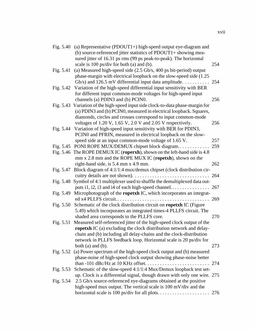
Fig. 5.40 (a) Representative (PDOUT1+) high-speed output eye-diagram and (b) source-referenced jitter statistics of PDOUT1+ showing mea-sured jitter of 16.31 ps rms (99 ps peak-to-peak). The horizontal scale is 100 ps/div for both (a) and (b). 254
Fig. 5.41 (a) Measured high-speed side (2.5 Gb/s, 400 ps bit-period) output phase-margin with electrical loopback on the slow-speed side (1.25 Gb/s) and 126.5 mV differential input data amplitude. . . . . . . . . . . 254
Fig. 5.42 Variation of the high-speed differential input sensitivity with BER for different input common-mode voltages for high-speed input channels (a) PDIN3 and (b) PCIN0. 256
Fig. 5.43 Variation of the high-speed input side clock-to-data phase-margin for (a) PDIN3 and (b) PCIN0, measured in electrical loopback. Squares, diamonds, circles and crosses correspond to input common-mode voltages of 1.20 V, 1.65 V, 2.0 V and 2.05 V respectively. 256
Fig. 5.44 Variation of high-speed input sensitivity with BER for PDIN3, PCIN0 and PFRIN, measured in electrical loopback on the slow-speed side at an input common-mode voltage of 1.65 V. 257
Fig. 5.45 PONI ROPE MUX/DEMUX chipset block diagram. . . . . . . . . . . . . 259Fig. 5.46 The ROPE DEMUX IC (roperxh), shown on the left-hand side is 4.8
mm x 2.8 mm and the ROPE MUX IC (ropetxh), shown on the right-hand side, is 5.4 mm x 4.9 mm. 262
Fig. 5.47 Block diagram of 4:1/1:4 mux/demux chipset (clock distribution cir-cuitry details are not shown). . . . . . . . . . . . . . . . . . . . . . . . . . . . . . . 264
Fig. 5.48 Symbol of 4:1 multiplexer used to shuffle the demultiplexed data out-puts i1, i2, i3 and i4 of each high-speed channel. . . . . . . . . . . . . . . . 267
Fig. 5.49 Microphotograph of the ropetxh IC, which incorporates an integrat-ed x4 PLLFS circuit. . . . . . . . . . . . . . . . . . . . . . . . . . . . . . . . . . . . . . 269
Fig. 5.50 Schematic of the clock distribution circuit on ropetxh IC (Figure 5.49) which incorporates an integrated times-4 PLLFS circuit. The shaded area corresponds to the PLLFS core. 270
Fig. 5.51 Measured self-referenced jitter of the high-speed clock output of the ropetxh IC (a) excluding the clock distribution network and delay-chain and (b) including all delay-chains and the clock-distribution network in PLLFS feedback loop. Horizontal scale is 20 ps/div for both (a) and (b). 273
Fig. 5.52 (a) Power spectrum of the high-speed clock output and (b) measured phase-noise of high-speed clock output showing phase-noise better than -101 dBc/Hz at 10 KHz offset. . . . . . . . . . . . . . . . . . . . . . . . . . 274
Fig. 5.53 Schematic of the slow-speed 4:1/1:4 Mux/Demux loopback test set-up. Clock is a differential signal, though drawn with only one wire. 275
Fig. 5.54 2.5 Gb/s source-referenced eye-diagrams obtained at the positive high-speed mux output. The vertical scale is 100 mV/div and the horizontal scale is 100 ps/div for all plots. . . . . . . . . . . . . . . . . . . . . 276

xviii
Fig. 5.55 2.5 Gb/s self-referenced (using the PLLFS trigger output as the os-cilloscope trigger) eye-diagrams obtained at the positive high-speed mux output. The vertical scale is 100 mV/div and the horizontal scale is 100 ps/div for all plots. 277
Fig. 5.56 Representative demultiplexed eye-diagrams of PDIN7 at 625 Mb/s/channel at the slow-speed outputs of the roperxh IC in Figure 5.38. D14_OUT_P and D14_OUT_N correspond to the half-speed clock outputs of the roperxh IC. The horizontal scale for all plots is 500 ps/div and vertical scale is 50 mV/div for all plots. . . . . . . . . . . . . . 278
Fig. 5.57 Variation of the roperxh IC high-speed input clock-to-data phase-margin for the outermost (squares) and the innermost (diamonds) in-put channels measured in electrical loopback on the slow-speed side. 279
Fig. 5.58 Source-referenced jitter statistics of (a) PDOUT3+ and (b) PDOUT7+. The horizontal scale is 50 ps/div for both (a) and (b). . 280
Fig. 5.59 Self-referenced jitter statistics of (a) PDOUT3+ and (b) PDOUT7+. The horizontal scale is 50 ps/div for both (a) and (b). 280
Fig. 5.60 ropetxh high-speed output phase-margin for the innermost (PDOUT1, diamonds) and outermost (PCOUT0, squares) channels measured in electrical loopback on the slow-speed side. . . . . . . . . . 282
Fig. 5.61 Overlaid high-speed data and clock eye-diagrams for each high-speed output corresponding to 231 - 1 NRZ PRBS patterns. The hor-izontal scale is 100 ps/div and the vertical scale is 100 mV/div for all plots. 283
Fig. 5.62 Skew (a) of 5 ps the outermost channels PDOUT7 (not displayed in panel) and PCOUT0 and (b) 25 ps between the outermost channel PCOUT0 (not displayed in panel) and the innermost channel PDOUT3. The horizontal scale is 50 ps/div for both (a) and (b).. . . 283
Fig. 5.63 Source-referenced PONI Tx-Rx 2.5 Gb/s optical eye-diagrams mea-sured (using the BERT trigger output as the oscilloscope trigger) at the positive high-speed optical outputs. The vertical scale is 100 mV/div and the horizontal scale is 100 ps/div for all eye-diagrams. 284
Fig. 5.64 Source-referenced jitter statistics of the Rx module output of channel 1 and channel 6 in the optical loopback setup, with a BERT as the electrical data source driving the Tx module inputs. The horizontal scale is 50 ps/div and the vertical scale is 50 mV/div for both (a) and (b). 285
Fig. 5.65 Schematic of the slow-speed loopback setup with optical loopback using the Agilent parallel optical Tx and Rx modules driven by the high-speed output of the ropetxh IC. Note that all the BER measure-ments are source-referenced. 287

xix
Fig. 5.66 Source-referenced 2.5 Gb/s optical eye-diagrams measured (using the BERT trigger output as the oscilloscope trigger) at the positive high-speed optical Rx module outputs. The vertical scale is 50 mV/div and the horizontal scale is 100 ps/div. . . . . . . . . . . . . . . . . . . . . 288
Fig. 5.67 Source-referenced jitter statistics of the optical Rx module corre-sponding to PDOUT3+ and PDOUT7+. The vertical scale is 50 mV/div and the horizontal scale is 100 ps/div for both (a) and (b). . . . . 289
Fig. 5.68 Self-referenced jitter statistics of the optical Rx module outputs cor-responding to PDOUT1+ and PDOUT7+. The horizontal scale is 50 ps/div and the vertical scale is 50 mV/div for both (a) and (b). . . . . 289
Fig. 5.69 Insertion-loss measurement of (a) slow-speed side evaluation board, (b) slow-speed side to high-speed side evaluation board and (c) high-speed side evaluation board.. . . . . . . . . . . . . . . . . . . . . . . . . . . 290
Chapter 6 . . . . . . . . . . . . . . . . . . . . . . . . . . . . . . . . . . . . . . . . . . . . . . . . . . . . . . . . 293
Fig. 6.1 Correspondence of discussion in this chapter to the OES IC block diagram in Figure 1.10. 294
Fig. 6.2 AC-schematic of VCSEL (a) current drive and (b) voltage drive. Rs is the VCSEL series resistance and CJ is the VCSEL capacitance. . 295
Fig. 6.3 (a) Schematic of VCSEL driver circuit whose eye-diagram at 3.3 Gb/s corresponding to 231 - 1 NRZ PRBS from the BERT is shown in (b). The measured insertion-gain is shown in (c). See text for de-tails. 298
Fig. 6.4 2.5 Gb/s 231 - 1 NRZ PRBS eye-diagram for LD L1 driven by BERT. 299
Fig. 6.5 2.5 Gb/s 231 - 1 NRZ PRBS eye-diagram for LD L1 (top waveform) and electrical output (lower waveform).. . . . . . . . . . . . . . . . . . . . . . 300
Fig. 6.6 1.25 Gb/s 231 - 1 NRZ PRBS eye diagram for LD L1 (top waveform) and electrical output (lower waveform).. . . . . . . . . . . . . . . . . . . . . . 301
Fig. 6.7 EO-OE LTF for typical OE data link with L1 and 10 db optical link-loss. 303
Fig. 6.8 EO-OE LTF for a typical OE data link with L2 and 10 dB optical link-loss. 304
Fig. 6.9 LTF of electrical link that can be supported by designed LVDS Rx-Tx circuitry in 0.5 µm CMOS at 2.5 Gb/s. . . . . . . . . . . . . . . . . . . . . 304
Fig. 6.10 Linear two-port representation of interconnect. . . . . . . . . . . . . . . . . 305Fig. 6.11 Block diagram of an asynchronous OE receiver . . . . . . . . . . . . . . . . 308Fig. 6.12 Block level diagram of synchronous optical receiver . . . . . . . . . . . . 310Fig. 6.13 Extension of synchronous and asynchronous receiver circuits to par-
allel synchronous OE data link. . . . . . . . . . . . . . . . . . . . . . . . . . . . . 311Fig. 6.14 Half-speed optical receiver array schematic with synchronous receiv-
ers. 312

xx
Fig. 6.15 Variation of F-3dBoverall /fu with the number of amplifier stages, n, for overall gain Go of 2, 4, 6 and 8. 313
Fig. 6.16 Variation of (a) F-3dBoverall /fu maximum with overall gain Go and (b) number of stages n required to achieve it. . . . . . . . . . . . . . . . . . 315
Fig. 6.17 Half-speed OE receiver array schematic with oversampling receivers adapted from [10][42] for a 1:4 demultiplexer array. . . . . . . . . . . . . 316
Fig. 6.18 Half-speed OE receiver array schematic with synchronous receivers and a PLL in the clock channel, assuming the degree of demultiplex-ing to be 4 and B to be bit rate of each data channel. . . . . . . . . . . . . 317
Fig. 6.19 Schematic of waveforms at the various nodes in phase-aligner exam-ple in Figure 6.18. . . . . . . . . . . . . . . . . . . . . . . . . . . . . . . . . . . . . . . . 318
Fig. 6.20 Example of differential ring oscillator with four stages to generate quadrature outputs in a PLLFS. 319
Fig. 6.21 Half-speed optical receiver schematic with synchronous receiver, as-suming degree of demultiplexing to be 4.. . . . . . . . . . . . . . . . . . . . . 323
Fig. 6.22 MOSFET noise model [183], showing noise sources considered in this work. . . . . . . . . . . . . . . . . . . . . . . . . . . . . . . . . . . . . . . . . . . . . . 325
Fig. 6.23 Rules R1 through R6 for the transposition of sources method of de-termining input-referred noise-current PSD of a linear two-port net-work. . . . . . . . . . . . . . . . . . . . . . . . . . . . . . . . . . . . . . . . . . . . . . . . . . 329
Fig. 6.24 Rule R7: pushing a voltage through a resistive divider. . . . . . . . . . . 330Fig. 6.25 Elementary TIA and its equivalent small-signal model. . . . . . . . . . . 330Fig. 6.26 Transformation of small signal model by transposition of noise
sources I1 and I2 from the output to the input. The transposed noise-current source I1 in parallel with a voltage source is neglected. 331
Fig. 6.27 Small-signal model after transposition of I2/gm in Figure 6.26 to in-put. 331
Fig. 6.28 AC-schematic and small-signal circuit with noise sources of a CS amplifier. 332
Fig. 6.29 Transposition of I1 in Figure 6.28 to the input.. . . . . . . . . . . . . . . . . 333Fig. 6.30 Transposition of all noise sources to the input. . . . . . . . . . . . . . . . . . 333Fig. 6.31 Final small-signal circuit of the CS amplifier showing all noise sourc-
es referred to the input. 334Fig. 6.32 AC-schematic of CG OE pre-amplifier. . . . . . . . . . . . . . . . . . . . . . . 340Fig. 6.33 Schematic of a CGTIA. . . . . . . . . . . . . . . . . . . . . . . . . . . . . . . . . . . . 342Fig. 6.34 Variation of OE pre-amplifier power consumption with -3dB fre-
quency of stage (=1.414*Bitrate assuming 3 stage overall amp). . . 346Fig. 6.35 Receiver input sensitivity variation with input stage bandwidth in
0.5 µm CMOS process technology, BER < 10-13, Γ=1.5 for varying (a) Cd and (b) fT. 348
Fig. 6.36 Receiver input sensitivity variation with input stage bandwidth for varying BER requirement and excess channel thermal-noise factor, Γ. 349

xxi
Fig. 6.37 Power consumption variation (mW) with input stage sensitivity for desired stage bandwidth of 2 GHz for (a) varying Cd at Leff = 0.5 µm and varying Leff, Vdd at Cd = 0.5 pF and (b) Rf = 1 KΩ for both cas-es. 349
Fig. 6.38 Power consumption variation (mW) with input stage sensitivity for desired stage bandwidth of 3.5 GHz, varying Cd, Leff, Vdd and Γ with Rf = 1 KΩ. 350
Fig. 6.39 Elementary TIA and its small-signal circuit.. . . . . . . . . . . . . . . . . . . 352Fig. 6.40 AC-diagram of CG OE pre-amplifier.. . . . . . . . . . . . . . . . . . . . . . . . 354Fig. 6.41 Plots of Equation 6.76 and Equation 6.80 for values of (a) β = 0.1 and
(b) β = 2.0 with m = 1, 2 and 8. 355Fig. 6.42 Plots of Equation 6.76 and Equation 6.80 for values of β = 0.9 with
m = 1, 2 and 8. 356Fig. 6.43 Plots of Equation 6.80 and modified Equation 6.81 for values of β =
0.9 with m = 1 and 8. Dashed lines correspond to Equation 6.80 and solid lines correspond to modified Equation 6.80. 357
Fig. 6.44 Plots of Equation 6.80 (solid line) and modified Equation 6.82 (dia-monds) for values of β = 0.9 with m = 8. Diamonds correspond to the corrected expression with CG pole accounted for f-3dB = 2 GHz and fT = 9.0 GHz. . . . . . . . . . . . . . . . . . . . . . . . . . . . . . . . . . . . . . . . 358
Fig. 6.45 AC-equivalent circuit of elementary TIA . . . . . . . . . . . . . . . . . . . . . 359Fig. 6.46 Small-signal model of the open-loop common-source amplifier in
Figure 6.45. Vdbm is the noise source modulating the drain of the active transistor M1. . . . . . . . . . . . . . . . . . . . . . . . . . . . . . . . . . . . . . 359
Fig. 6.47 Plots of the full CGTIA sensitivity expression (Equation 6.99 and Equation 6.35) (solid line), full CSTIA sensitivity (Equation 6.91 and Equation 6.35) (dash dot line) and the CGTIA sensitivity ex-pression without taking the CG pole into account. 0.5 µm CMOS values of m = 8, k = 4, ωT = 44 Grad/s, A = 5, Γ = 1.5, BER < 10-13, Cd = 500 fF and Cp = 0 fF are used. 365
Fig. 6.48 Plots of full CGTIA sensitivity expression (Equation 6.99 and Equa-tion 6.35). (a) covers k = 1, 2, 4, 8 for m=8 and (b) shows k = 0.25, 1, 4 for m=8. 365
Fig. 6.49 Plots of full CGTIA sensitivity expression (Equation 6.99 and Equa-tion 6.35). (a) covers the variation of m from 1,4,8,16 for k = 4 and (b) shows the penalty accrued due to Cp= 0, 100, and 300 fF for k=4, m=8, Cd=500 fF. 366

xxii
Fig. 6.50 Plots of full CGTIA sensitivity expression (Equation 6.99 and Equa-tion 6.35) (solid line), full CSTIA sensitivity (Equation 6.91 and Equation 6.35) (dotted line) and the CGTIA sensitivity expression without taking the CG pole into account (dash dot line) for 0.1 µm CMOS process technology with m = 8, k = 4, fT = 100 GHz, Cp = 0, Γ = 2.5 and BER < 10-13 for the case of (a) Cd = 500 fF and (b) Cd = 100 fF. 367
Fig. 6.51 Plots of exact CGTIA sensitivity expression (Equation 6.99 and Equation 6.35) (solid line), full CSTIA sensitivity (Equation 6.91 and Equation 6.35) (dash-dot line), the exact CGTIA sensitivity ex-pression with induced gate-noise (dash dot line) and the full CSTIA sensitivity expression with induced gate-noise for 0.5 µm CMOS process technology with λ = 850 nm, η = 0.8, m = 8, k = 4, ωT = 44 Grad/s, Cd=500 fF, Cp = 0, Γ = 1.5 and BER < 10-13. 368
Fig. 6.52 Plots of exact CGTIA sensitivity expression (Equation 6.99 and Equation 6.35) (solid line), full CSTIA sensitivity (Equation 6.91 and Equation 6.35) (dash-dot line) and the exact CGTIA sensitivity expression which accounts for a bias resistor Rs = 1.82 KΩ in paral-lel with the photodiode (dotted line) for 0.5 µm CMOS process tech-nology with λ = 850 nm, η = 0.8, m = 8, k = 4, ωT = 44 Grad/s, Cd = 500 fF, Cp = 0, Γ = 1.5 and BER < 10-13. 369
Fig. 6.53 Schematic illustration of the influence of the front-end inductor on the input-referred noise-current PSD i2ckt. The transposition is achieved by using rules R5 and R3 described in Figure 6.23. . . . . . 371
Fig. 6.54 AC-schematic of single-ended CG OE receiver front-end.. . . . . . . . 371Fig. 6.55 Schematic illustration of possible realizations of (a) single-ended and
((b) and (c)) differential receivers, all of which operate with light signal from a single fiber. . . . . . . . . . . . . . . . . . . . . . . . . . . . . . . . . . 375
Fig. 6.56 AC-schematic of the differential CG OE receiver. . . . . . . . . . . . . . . 376Fig. 6.57 Schematic illustration of bias servoing using a dummy amplifier . . 378Fig. 6.58 Coupled planar transformer to increase effective inductance by neg-
ative mutual coupling (a) and positive mutual coupling (b). . . . . . . 381Fig. 6.59 Schematic of TIA implemented by differential cascoded amplifier
with shunt-shunt feedback. 384Fig. 6.60 Schematic of DC-restorer circuit implemented by differential cascod-
ed amplifier with gmboosting and shunt-shunt feedback. . . . . . . . . 384Fig. 6.61 Schematic of Cherry-Hooper limiting amplifier with APLSD load
(insert (Figure 3.10)) and cross-coupled pair to broadband the am-plifier. 385
Fig. 6.62 Schematic of controlled-peaking amplifier implemented with regu-lated cascode amplifier input stage followed by output stage with controlled zero insertion by control signal srcntrl. . . . . . . . . . . . . . . 386
Fig. 6.63 Schematic of differential retiming circuit.. . . . . . . . . . . . . . . . . . . . . 387

xxiii
Fig. 6.64 Schematic of merged 2:1 multiplexer and limiting amplifier in Figure 6.61. 388
Fig. 6.65 Micro-photograph of OE receiver array in 0.5 µm CMOS technology. The submitted layout size is 6.40 mm x 2.7 mm and the IC die size is 6.85 mm x 2.9 mm. 389
Fig. 6.66 Schematic of latched TIA array. . . . . . . . . . . . . . . . . . . . . . . . . . . . . 390Fig. 6.67 Measured sensitivity curves for 1.5 Gb/s, 2.0 Gb/s and 2.5 Gb/s for
(a) 27 - 1 and (b) 223 - 1 NRZ PRBS input data patterns.. . . . . . . . . 392Fig. 6.68 Measured sensitivity curve for the latched TIA at 2.5 Gb/s for 27 - 1,
223 - 1 and 231 - 1 NRZ PRBS input data patterns. The insert shows the eye diagram of the channel output at a BER < 10-12 for -16 dBm 231 - 1 NRZ PRBS input data patterns and -16 dBm clock inputs from the BERT. 392
Fig. 6.69 Measured sensitivity curve for a representative OE receiver array channel at 2.0 Gb/s for 27 - 1, 223 - 1 and 231 - 1 NRZ PRBS input data patterns. The insert shows the electrical output eye diagram at a BER < 10-12 for -19 dBm 231 - 1 NRZ PRBS input data patterns and -19 dBm clock inputs. 393
Fig. 6.70 Measured sensitivity curve for a representative OE receiver array channel at 1.5 Gb/s for 27 - 1, 223 - 1 and 231 - 1 NRZ PRBS input data patterns. The insert shows the electrical output eye diagram at a BER < 10-12 for -19 dBm 231 - 1 NRZ PRBS input data patterns and -19 dBm clock inputs. 393
Fig. 6.71 Measured output jitter of a representative OE channel at (a) 2.5 Gb/s for -16 dBm and (b) 1.5 Gb/s for -19 dBm 231 - 1 NRZ PRBS input data patterns and clock signals. The jitter is measured to be (a) 12.47 ps rms (82 ps peak-to-peak) and (b) 14.35 ps rms and 94 ps peak-to-peak. 394
Chapter 7 . . . . . . . . . . . . . . . . . . . . . . . . . . . . . . . . . . . . . . . . . . . . . . . . . . . . . . . . 396
Fig. 7.1 Proven design point of 25 Gb/s in 0.5 µm CMOS process technology over 12-wide MMF-ribbon with 10 channels of data. 396
Fig. 7.2 Block diagram of 12 channel 100 Gbit/s WDM link leveraging ad-vances in parallel OE data links. 397
Fig. 7.3 (a) Eye-safe power levels for wavelengths between 700 and 1400 nm and (b) Dispersion curves for wavelengths between 1000 and 1600 nm for SMF with zero chromatic dispersion at 1300 nm. . . . . . . . . 398
Fig. 7.4 Proposed design point of 100 Gb/s Ethernet in 0.1 µm CMOS process technology using WDM in SMF-ribbon using 12 wavelengths at 1300 nm center wavelength. . . . . . . . . . . . . . . . . . . . . . . . . . . . . . . . 399

xxiv
Fig. 7.5 Optical sensitivity of a CS and CG receiver in 0.1 µm CMOS with η=0.8, λ = 1.3 mm, fT = 40 GHz, Cd= 300 fF, Cp=100 fF, Γ = 2.5, T = 358 °K and Rd1 = 200 Ω. 402
Fig. 7.6 AC schematic of differential CG receiver front-end. . . . . . . . . . . . . 403
Appendix A VTT Specification . . . . . . . . . . . . . . . . . . . . . . . . . . . . . . . . . . . . . . . 431
Fig. A-1 Block diagram of Termination Voltage in Data Link . . . . . . . . . . . . 431Fig. A-2 Schematic of current sinking termination voltage.. . . . . . . . . . . . . . . 432
Appendix B Testing Methodology . . . . . . . . . . . . . . . . . . . . . . . . . . . . . . . . . . . . 433
Fig. B-1 BER test setup of a representative circuit. . . . . . . . . . . . . . . . . . . . . . 434

xxv
List of Tables
Chapter 1. . . . . . . . . . . . . . . . . . . . . . . . . . . . . . . . . . . . . . . . . . . . . . . . . . . . . . . . . . 1
Chapter 2. . . . . . . . . . . . . . . . . . . . . . . . . . . . . . . . . . . . . . . . . . . . . . . . . . . . . . . . . . 35
Table 2.1 Reported serial and parallel data links. . . . . . . . . . . . . . . . . . . . . . . . 40Table 2.2 Reported data link design approaches. . . . . . . . . . . . . . . . . . . . . . . . 41Table 2.3 Advantages and disadvantages of receiver design approaches. . . . . 42
Chapter 3. . . . . . . . . . . . . . . . . . . . . . . . . . . . . . . . . . . . . . . . . . . . . . . . . . . . . . . . . . 47
Table 3.1 Measured maximum frequency of operation of each setting of the 4/5, 4/5/6 and 4/6 prescalers on testdie T7. . . . . . . . . . . . . . . . . . . . . . . . 88
Table 3.2 PECL/ECL IO circuits. . . . . . . . . . . . . . . . . . . . . . . . . . . . . . . . . . . 112Table 3.3 Comparison of LVDS and PECL Transmit circuits in parallel load
termination configuration. . . . . . . . . . . . . . . . . . . . . . . . . . . . . . . . . . 118Table 3.4 Summary of measurements of setup S-1 when VTT_Rx=VTT_Tx =
common-mode voltage of input and output signals. . . . . . . . . . . . . . 121
Chapter 4. . . . . . . . . . . . . . . . . . . . . . . . . . . . . . . . . . . . . . . . . . . . . . . . . . . . . . . . . . 124
Table 4.1 Setting descriptions for T8 VCO measurements . . . . . . . . . . . . . . . 173
Chapter 5. . . . . . . . . . . . . . . . . . . . . . . . . . . . . . . . . . . . . . . . . . . . . . . . . . . . . . . . . . 212
Table 5.1 Power Terminal Description of PONIMUX IC. . . . . . . . . . . . . . . . . 241Table 5.2 Measured characteristics of the high-speed clock input waveforms in
Figure 5.39 (a), (b), and (c). . . . . . . . . . . . . . . . . . . . . . . . . . . . . . . . 253Table 5.3 Summary of the logic operation of the aligner-control circuit in re-
sponse to the demultiplexed frame channel outputs f1, f2, f3 and f4. 268Table 5.4 ropetxh times-4 PLLFS self- and source-referenced jitter. . . . . . . 271Table 5.5 Measured output jitter for different channels in slow-speed loopback. 281Table 5.6 Measured jitter of each parallel optical Rx module output. . . . . . . . 286
Chapter 6. . . . . . . . . . . . . . . . . . . . . . . . . . . . . . . . . . . . . . . . . . . . . . . . . . . . . . . . . . 293
Table 6.1 Area Power specifications . . . . . . . . . . . . . . . . . . . . . . . . . . . . . . . . 307
Chapter 7. . . . . . . . . . . . . . . . . . . . . . . . . . . . . . . . . . . . . . . . . . . . . . . . . . . . . . . . . . 396

xxvi
Table 7.1 Simulated and measured sensitivity at error-free data rate correspond-ing to the bandwidth of different CMOS OE receiver. . . . . . . . . . . . 404
xxvii
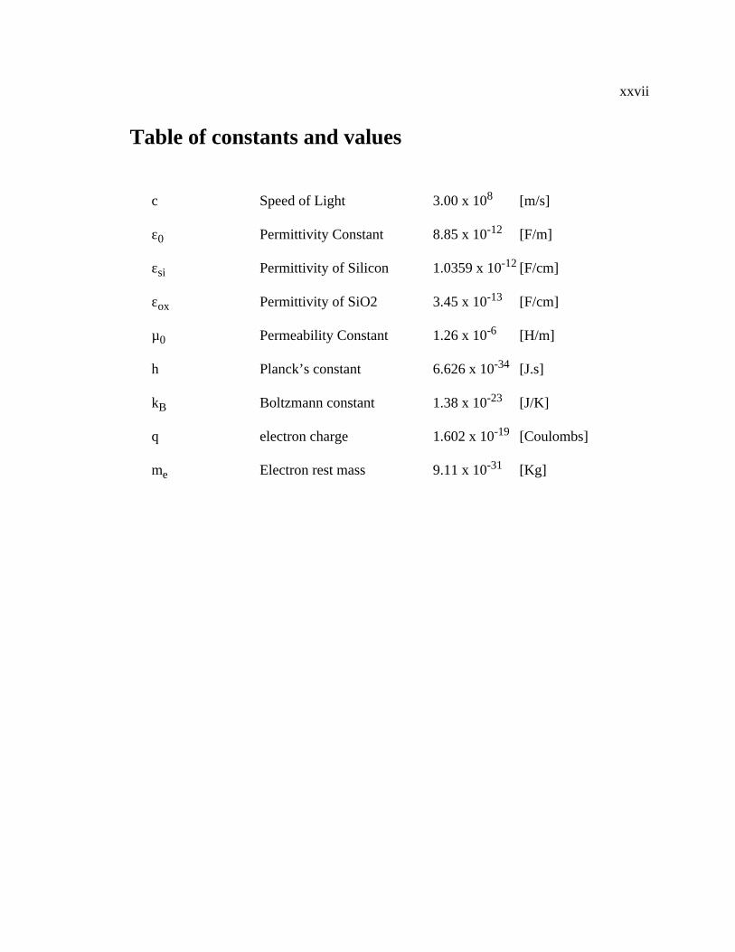
Table of constants and values
c Speed of Light 3.00 x 10⁸ [m/s]
ε0 Permittivity Constant 8.85 x 10⁻¹² [F/m]
εsi Permittivity of Silicon 1.0359 x 10⁻¹² [F/cm]
εox Permittivity of SiO2 3.45 x 10⁻¹³ [F/cm]
µ0 Permeability Constant 1.26 x 10⁻⁶ [H/m]
h Planck’s constant 6.626 x 10⁻³⁴ [J.s]
kB Boltzmann constant 1.38 x 10⁻²³ [J/K]
q electron charge 1.602 x 10⁻¹⁹ [Coulombs]
me Electron rest mass 9.11 x 10⁻³¹ [Kg]

xxviii
List of Symbols
C Capacitance [F]CL Load capacitance [F]Cg Gate capacitance [F]Cgn Gate capacitance of an NMOS transistor [F]Cgp Gate capacitance of a PMOS transistor [F]en Voltage noise density [V/ ]E Electric Field [V/m]f Frequency [Hz]f3 -3dB Bandwidth [Hz]fL Loop Bandwidth [Hz]fo Oscillation frequency [Hz]fout Output frequency [Hz]fT Unity current gain frequency of MOS transistor [Hz]fTn Unity current gain frequency of an NMOS transistor[Hz]fTp Unity current gain frequency of a PMOS transistor [Hz]f(t) Frequency modulated over time [Hz]Hn(s) Phase noise transfer function through PLLFS loopHs(s) Phase signal transfer function through PLLFS loopI Current [A]Ids Drain to source current in MOS transistor [A]Igg Gate current in MOS transistor [A]Iss Differential pair tail current [A]In Noise current [A]Io DC bias current [A]in Current noise density [A/ ]jk Boltzmann’s constant [J/K]K PLLFS loop transfer function constant [rad/s]Ko VCO voltage to frequency transfer function constant[rad/V.s]Kh PLLFS loop filter transfer function constantKd PLLFS PFD transfer function constant [V/rad]L Inductance [H]Ln Channel length of an NMOS transistor [m]Lp Channel length of a PMOS transistor [m]P Power [Watt]q Electron charge [Coulombs]Q Quality factor for a second order systemQ Signal to Noise RatioR Resistance [Ω]
Hz
Hz
1–

xxix
RAC AC-Resistance [Ω]RDC DC-Resistance [Ω]s Laplace complex frequency [rad/s]Sφ(f) Phase noise PSD [rad2/Hz]SφCL(f) Phase noise PSD [rad2/Hz]SφOL(f) Phase noise PSD [rad2/Hz]t Time [s]tox Gate oxide thickness of MOS transistor [m]tr Rise time [s]tf Fall time [s]tdav Average delay [s]Τ Period [s]Τ Temperature [°K or °C]Td Delay [s]To Period corresponding to frequency fo [s]V Voltage [V]Vdd Power-supply voltage [V]Vcntl VCO control voltage [V]Vgs Gate to source voltage of MOS transistor [V]Vds Drain to source voltage of MOS transistor [V]Vsb Source to bulk voltage of MOS transistor [V]Vdg Drain to gate voltage of MOS transistor [V]Vdm PFD voltage output [V]Vin Input voltage [V]Voff Offset voltage [V]Vt Threshold voltage [V]Vtn Threshold voltage of an NMOS transistor [V]Vtp Threshold voltage of a PMOS transistor [V]Vtrig Voltage waveform for CSA trigger [V]Vo Voltage amplitude [V]V(t) Voltage varying over time [V]W MOS transistor channel width [m]Wn NMOS transistor channel width [m]Wp NMOS transistor channel width [m]Y Admittance [S]Z Impedance [Ω]Zin Input impedance [Ω]Zo Output impedance [Ω]α Noise scaling factor (from Abidi and Meyer)εox Permittivity of gate oxide in CMOS process [F/cm]∆φ rms frequency deviation [s]∆Τ Delay time for jitter measurement [s]θeo PLLFS static phase error [rad]

xxx
θi PLLFS input phase [rad]θni PLLFS input phase noise [rad2/Hz]θn PLLFS phase noise [rad]θo PLL output phase [rad]θno PLL output phase noise [rad2/Hz]λ wavelength [m]ρ Resistivity [Ωm]θj Junction Temperature [K]σ Standard deviation of a distributionσ Conductivity [Mho]σ2 Variance of a distributionσt Standard deviation of time errors [s]τL Time constant associated with loop bandwidth fL [s]τn Channel transit for an NMOS transistor [s]τp Channel transit for a PMOS transistor [s]φ Phase [rad]φ0 Initial phase [rad]φ(t) Phase as a function of time [rad]µ Mobility of carriers in MOS transistor channel [cm2/V.s]µ Magnetic permeability of material [Henry/m]µn Mobility of electrons in NMOS transistor channel [cm2/V.s]µp Mobility of holes in PMOS transistor channel [cm2/V.s]ξ Damping constant for second order systemω Angular Frequency [rad/s]ωn Angular natural frequency [rad/s]ωo Angular oscillation frequency [rad/s]ωout Angular output frequency [rad/s]ω(t) Variation of angular frequency with time [rad/s]

xxxi
List of Abbreviations and Acronyms
AC Alternating CurrentAGC Automatic Gain ControlAGP Accelerated Graphics ProtocolAM Amplitude ModulationAOC Automatic Offset ControlAPD Avalanche Photo-DiodeAPLS Active Pulldown Level ShiftAPLSD Active Pulldown Level Shifted DiodeASIC Application Specific Integrated CircuitATM Asynchronous Transfer ModeBER Bit Error RatioBERT Bit Error Ratio TesterBR Bit RateBW BandWidthCCCS Current Controlled Current SourceCCO Current Controlled OscillatorCG Common GateCHE Channel Hot ElectronsCMFB Common Mode FeedBackCMFN Common Mode Feedback NetworkCML Current Mode LogicCMOS Complementary Metal Oxide SiliconCLM Channel Length ModulationClk ClockCP Charge PumpCS Common SourceCSA Communications Signal AnalyzerDC Direct CurrentDCVSL Differential Cascode Voltage Switch LogicDCFL Direct Coupled Fet LogicDFF Data Flip-FlopDIBL Drain Induced Barrier LoweringDLL Delay Locked LoopDPFD Digital Phase Frequency DetectorECL Emitter Coupled LogicEO Electro-OpticEOP End Of PacketEStore Elastic StoreFIFO First-In First-Out memoryFIR Finite Impulse ResponseFD Frequency Detector

xxxii
FF Flip-FlopFM Frequency ModulationFS Frequency SynthesizerFWHM Full Width Half MaximumGaAs Gallium ArsenideGbps Giga bit per secondGBps Giga Byte per secondGBW Gain BandWidth productGRIM Ground-Reference Impedance MatchedGRps Giga Radians per secondGLVDS GRIM Low Voltage Differential SignalsGPB General Purpose BoardGTL Gunning Transistor LogicHBT Hetero-junction Bipolar TransistorHEMT High Electron Mobility TransistorHP Hewlett-PackardHSTL High-Speed Transceiver LogicIC Integrated CircuitInP Indium PhosphideIO Input/OutputISI Inter-Symbol InterferenceKb KilobitKB KiloByteLA Link AdapterLP Link PerformanceLTF Link Transmission FigureLVDS Low Voltage Differential SignalsLVIC Linear V to I ConvertorMbps Mega bit per secondMBps Mega Byte per secondMCM Multi-Chip ModuleME Mux-EncodeMM Multi-ModeMMF Multi-Mode FiberMNE Mux No-EncodeMOSIS Metal Oxide Semiconductor Implementation ServiceMSM Metal Semiconductor MetalMQW Multiple Quantum WellNIC Network Interface Chip.NME No-Mux EncodeNMNE No-Mux No-EncodeNMOS N channel Metal Oxide SemiconductorNRZ Non-Return to Zero

xxxiii
ODL Optical Data LinkOE Opto-ElectronicOEIC Opto-Electronic Integrated CircuitOES Opto-Electronic SystemOTA Operational Transconductance AmplifierP2P Point to PointPAM Pulse Amplitude ModulationPCB Printed Circuit BoardPCI Peripheral Component InterconnectPD Phase DetectorPFD Phase Frequency DetectorPECL Positive Emitter Coupled LogicPFD Phase Frequency DetectorPIN P-type Insulator N-type PLL Phase Locked LoopPLLFS Phase Locked Loop Frequency SynthesizerPM Phase ModulationPMOS P channel Metal Oxide SemiconductorPODL Parallel Optical Data LinkPOLO Parallel Optical Link OrganizationPONI Parallel Optical Network InterfacePRBS Pseudo-Random Bit SequencePSD Power Spectral DensityPTAT Proportional To Absolute TemperatureQAM Quadrature Amplitude ModulationQFP Quad-Flat PackRAM Random Access MemoryRF Radio FrequencyRZ Return to ZeroRx ReceiveSAW Surface Acoustic WaveSCI Scalable Coherent InterconnectSCMOS Scalable CMOSSONET Synchronous Optical NETworkSMF Single Mode FibreSNR Signal to Noise RatioSRAM Static Random Access MemorySS Shunt-ShuntSSN Simultaneous Switching NoiseTTL Transistor to Transistor LogicTSPC True Single Phase ClockingTx TransmitUI Unit Interval

xxxiv
VCO Voltage Controlled OscillatorWDM Wavelength Division MultiplexingWSS Wide-Sense StationaryXOR eXclusive-ORamp amplifierdemux demultiplexermux multiplexerpk2pk peak-to-peakpreamp pre-amplifierrms root mean square

xxxv
Abstract
It is well-known that the increase in signaling rates of scaled CMOS transistor circuits
has not been matched by an appropriate increase in the high-frequency performance of
integrated circuit packaging and interconnect. A successful opto-electronic solution
intimately integrated with CMOS requires that the power, bandwidth and form-factor
advantages of opto-electronics must be first demonstrated. In this dissertation, we use
0.5 µm CMOS process technology to demonstrate an all-CMOS parallel opto-electronic
data link, whose link performance is better than that of a parallel electrical interface.
This dissertation addresses the key circuit challenges of receiver design
accommodating critical parameters of high input-sensitivity, low crosstalk, low-power
consumption, high bit-rate, isolation of sensitive analog circuitry from the noise generated
on the power, ground and substrate nodes of the IC, high-frequency clock generation and
distribution, minimization of the impact of jitter introduced by the electronics and optics
on link data integrity, skew compensation, and effective utilization of the bandwidth
offered by parallel fiber-optic media.
An 8.8 W, 11-wide 2.5 Gb/s/channel 4:1/1:4 multiplexer/demultiplexer chipset, with
an integrated times-4 PLLFS with sub-50 ps peak-to-peak jitter which matches the
performance of CMOS systems to the interconnect, as well a 3.7 W 12-wide 2.5 Gb/s/
channel opto-electronic receiver and transmitter array in 0.5 µm CMOS, which are key
components of CMOS opto-electronic interface circuitry, are demonstrated. These results
are used to propose a solution for a 100 Gb/s parallel optical data link in 0.1 µm CMOS
process technology.

1
Chapter 1
Introduction
1.1 Motivation
Complementary Metal Oxide Semiconductor (CMOS) device sizes have been
shrinking continuously in reasonable agreement with Gordon Moore’s law [1], an
observation of a trend in the semiconductor industry that the number of CMOS transistors
in an IC approximately doubles every eighteen months. The smallest feature size CMOS
process technology announced so far is 0.07 µm CMOS [2], where it is reported that the
delay of a ring-oscillator delay cell is 7.8 ps. This continued reduction in transistor sizes is
unlikely to be sustained far into the future as evidenced by the fact that Moore’s law
predicts the DRAM cell size to be less than that of an atom by the year 2020.
This in all likelihood means that future system performance improvement will
continue at an equivalent rate of Moore’s law by improvements in architecture and
interconnect technologies. Increasing clock speeds in today’s PCs due to advances in
device technology have resulted in more and more transistors being used for buffers.
These transistors can be viewed as “wasted” transistors which better architectures,
packaging and interconnect solutions can make use of. Although the continued reduction
in CMOS sizes in the future is going to be limited by device sizes becoming close to
atomic dimensions and device performance being dominated by quantum effects, the need
for higher Integrated Circuit (IC) Input/Output (I/O) pin-count and bandwidth has become

2
a significant challenge. As process technologies shrink, the number of IO pins needed per
IC increases due to increased system functionality that is integrated onto a single IC. The
computational speed of ICs increases due to the decrease in transistor size and the
consequent decrease in the transistor gate delay [3], which in turn drives the need for
higher IO pin bandwidth. Thus, there is a need for higher IO pin counts and higher
bandwidth per pin.
The Semiconductor Industry Association (SIA) 1997 roadmap [4] in Figure 1.1 plots
the consensus expectation in the industry as of 1997 on the decrease in minimum feature
size (plotted against the left vertical axis (in nm) with squares), the off-chip high
performance multiplexed bus (diamonds) signaling frequency and the non-multiplexed
peripheral bus (triangles) signaling frequency (plotted against the right vertical axis (in
GHz)) with the calendar year. The increase in signaling rates of scaled CMOS transistor
Figure 1.1: SIA 97 Roadmap indicating reduction in minimum device feature size (vertical axis on left side, squares), off-chip high performance multi-plexed bus frequency (vertical axis on right side) (diamonds) and off-chip peripheral bus frequency (triangles).

3
circuits has not been matched by an appropriate increase in high-frequency performance
of integrated circuit packaging and interconnect. In addition, system-level integration has
failed to significantly increase volume packing density or edge-connection density (form-
factor) [5].
The steady shrink of CMOS process technology feature sizes has resulted in the
increase of reported maximum date rates for single channels from 2.5 Gb/s in 0.8 µµm
CMOS [10] to 4.0 Gb/s in 0.5 µm CMOS [10][11]. These data-rates will increase as
device sizes shrink because of the increase in device transconductance associated with
smaller device geometries. The transmission of higher data-rates between ICs increasingly
runs into the distance-dependent capacity problem of electrical interconnects due to skin-
effect and dielectric losses. The necessity of transmission over matched-impedance
transmission lines requires increased power dissipation. Attempts to address these
problems [10][11][12] have shortcomings. Dally and Poulton [11] proposed the idea of
equalizing the signal that is launched from the IC to compensate for losses and distortion
in the transmission medium. Transmit signal pre-emphasis has been successfully used to
implement a 1.0625 Gb/s transceiver operating over a 30 m 50 Ω cable link [14].
Compensation mechanisms like multiple-sampling [10], transmitter equalization [11] and
signal-pre-emphasis have area and power overheads. The implementation of the signaling
system described in [11] achieved a BER of only about 10-4 at 2.5 Gb/s over 1 m of AWG
30 twisted-pair line [12]. Additionally, the loss and distortion of these transmission media
increases dramatically as the bit rate increases, and it is not clear that the above
mechanisms can effectively be utilized in a parallel interface because of interconnect
skew, without going to the extreme solution of clock and data recovery circuits for every
line. Signal losses and crosstalk requirements seriously constrain the form-factor that can
be achieved by electrical interconnect.

4
The need for larger IO pin counts can be partially offset by a migration to area-based
interconnect with flip-chip bonding. The corresponding increase in routing density at the
Printed Circuit Board (PCB) level increases the potential for crosstalk between signal
traces, forcing a trade-off between attenuation (and therefore, transmission distance) in
signal traces and routing density, for a fixed amount of crosstalk that can be tolerated by
adjacent signal traces.
When the distance travelled by the signal is longer than a tenth of the wavelength in
the medium of propagation, we need controlled-impedance transmission lines to
propagate the signal. For a signal that requires a bandwidth of 1 GHz (a pulse with 10 -
90% rise-time of 350 ps in a single-pole system), a tenth of the wavelength is
approximately 1 cm for a material with εr = 9 (refractive index n = 3). PCBs typically use
a glass-fiber epoxy laminate called Fire-Retardant 4 (FR4). A tenth of the wavelength in
FR4 with εr = 4.6 (refractive index n = 2.15) corresponds to 1.4 cm. If the constraints on
the signal rise- and fall-times, and reflections are relaxed, it may be possible to tolerate a
distance as long as a fourth of the wavelength, giving a distance of only 3.5 cm for the
same signal. As a rule of thumb, transmission line phenomena become significant when
the rise-time of the signal is less than 2.5 times the time of flight of the signal [8].
It is therefore clear that higher IO bandwidth will require signals to be transmitted on
controlled impedance lines depending on distance. This requires controlled signal trace
widths, dielectric thickness, and dielectric permittivity on the PCB. Dense packing of
these controlled impedance lines, be they in the form of microstrips or striplines, will have
to deal with the problems of skin-effect loss, dielectric loss, and crosstalk. Skin-effect and
dielectric loss considerations limit the distance that the signals can be propagated before
pulse distortion and attenuation prevent data recovery. Signal attenuation imposes an
upper bound on the packing density of these interconnects. The need for larger IO pin
counts can be mitigated to a certain extent by multiplexing parallel data lines from the IC

5
prior to transmission followed by demultiplexing at the receive side. This, however, drives
up the bandwidth utilization of the transmission line. The signal can only travel shorter
distances compared to the case of not using multiplexers and demultiplexers due to the
increased signal attenuation.
Rent’s rule is a useful empirical power law which relates the number of gates in a
system to the number of system IO interconnects. It states that the number of gates in a
system is equal to (IO/k)c, where k represents the sharing among interconnects and c is a
constant. Due to practical issues associated with design complexity, verification,
fabrication, yield, economies of scale, etc., large systems are usually created from a
number of smaller ICs which are interconnected at various hierarchical levels instead of
integrating the whole system onto a single IC. These hierarchical levels are Multi-Chip
Modules (MCMs), High Performance MCMs, PCBs, multiple PCBs in a shelf, multiple
shelves in a frame, and multiple frames in a room or building. Typical examples of such
large complex systems are telephone switches, dense web-server installations with
thousands of servers, routers and disk arrays, and large multiprocessor systems. Rent’s
rule is used to quantify the system IO count requirement of the different packaging
solutions of a large gate-count system for different levels of hierarchical partitioning
ranging from a single IC to a frame with multiples shelves of PCBs with surface mount
ICs. Taking, for example, a system with approximately 100 million gates, Figure 1.2
shows system IO (which is assumed to be represented by (IO/k)1.8, where k takes on
values depending on the hierarchical level of system organization) as a function of the
number of gates per IC for different hierarchical levels of system organization [13]. The
horizontal axis represents the gate density per chip in millions and the vertical axis
represents the IO requirement in thousands. Note that the graph is a log-log plot. The
application of Rent’s rule to determine the IO count needed for a single IC with 100
million transistors gives us 14000 IO from Figure 1.2. The impracticality of one IC with

6
100 million transistors and 14000 IO gives rise to systems which are made up of many
ICs, each of which is between 0.1 and 10 million transistors which are packaged and
interconnected at the MCM or PCB level. PCB IOs are located at the PCB edge. IO flows
between PCBs in the shelves that house them, which in turn, are housed in frames or
racks. To quantify the situation, a metric of edge-connection data-bandwidth density
(units of gigabits per second per centimeter or inch) is helpful, which indicates the
efficiency of a linear dimension for data transfer. We develop such a metric in Chapter 5.
Today’s electrical interconnect solutions like SCI [15] and HIPPI-6400 [16], PCI
[105] and AGP [106], fail to deliver the needed edge-connection data-bandwidth density,
resulting in an IO bottleneck at the board-level and system-to-system interconnect level.
Multi-shelf in a frame
Gate density per chip in millions0.01 0.1 1.0 10 100
IO te
rmin
als
requ
ired
in th
ousa
nds
0.01
0.1
1.0
10
100
1000
Packaging option
Multi-PCB in a shelfMulti-HPMCM on PCBHigh performance multi-chip moduleSurface mount on PCB
1460 IO from PCB900 IO from MCM 3260 IO from MCM
5300 IO from PCB
3D HPMCM
k=0.1 for frame (six shelves max)
k=0.2 for shelf (ten PCBs max)
k=0.3 for PCB (four HPMCM max)
k=0.4 for HPMCM (ten ICs max)
k=0.5 for IC
Frame
IC
Total IC
Figure 1.2: Rent’s rule for large system IO. k represents sharing of interconnects [13].
14,000 IO
HPMCM
PCBShelf

7
The HP 785/J7000 workstation, a state-of-the-art machine released in late 1999, uses a 4-
layer flex connector to connect the processor and I/O boards with an edge-connection
data-bandwidth density of 15.6 Gb/s/cm. This is to be contrasted with a 12-channel
mux/demux IC in 0.5 µm CMOS process technology (Chapter 5) that has an edge-
connection data-bandwidth density of 55 Gb/s/cm [18].
1.2 Electrical Interconnect Loss
Board to board and system to system inter-connectivity is through cables, which may
be matched impedance or simple twisted-pair, depending on the distance and data-rates
involved. Coaxial cable can be used for data transmission between systems or boards
when transmission line effects are important. Depending on the materials and the
construction of the cable, the frequency response of the cable can vary for a fixed distance.
The transfer function of a coaxial cable of resistance R per unit length, capacitance C
per unit length, inductance L per unit length, and conductance G per unit length, can be
modeled as [191]
(1.1)
where γ is the propagation constant of the line, whose real and imaginary parts are repre-
sented by α and β in Equation 1.2
(1.2)
α, the attenuation factor, is defined as
(1.3)
β, the imaginary part of Equation 1.2, contributes to the phase of the travelling wave in the
transmission line.
H ω( ) e γL–=
γ R jωL+( ) G jωC+( ) α jβ+= =
α Re γ( ) Re R jωL+( ) G jωC+( )×= =

8
Converting the transfer function to dB, we get
(1.4)
where R is chosen as RAC (Equation 1.6) instead of RDC (Equation 1.5) for computational
simplicity in Equation 1.3 when RAC exceeds RDC.
The DC resistance of the wire is
(1.5)
where σ is the conductivity of the material and d is the inner diameter of the coaxial cable
as shown in RAC. The skin-effect resistance RAC is
(1.6)
where µ is the permeability of free space and σ is the conductivity of the inner conductor
material (typically, copper).
Figure 1.3 shows the loss in dB/m of a circular cross-section Sucoflex SF104 coaxial
cable whose -3 dB bandwidth is beyond 40 GHz for a length of 1.0 m. Figure 1.3 shows
P dB m⁄( ) 20 H ω( )log 20αL( ) 10ln( )⁄–= =
RDC 4 πσd2
⁄=
RAC1d--- µf
πσ-------=
d D
(b) Geometry of the coaxial cable with
d = 55 mils, D = 160 mils, εr = 1.65
(low-density PTFE) and tan δ = 0.0003.
(a) Loss (dB/m) vs. Frequency for Coax (Sucoflex SF104)
Calculated
Measured
Figure 1.3: Circular cross-section coaxial cable loss with frequency [191].

9
both the measured and calculated curves for the cable whose dimensions are indicated in
the Figure 1.3 (b). This cable, with connectors, costs about a hundred dollars per meter in
quantities of a thousand. It is conceivable to use these cables in large systems, but cost,
form-factor, packaging, and connection density factors weigh heavily against their use.
Additionally, cable flexure changes the impedance, giving rise to reflections. Competitive
coaxial cable solutions have higher loss as a function of distance due to the use of smaller
inner-diameter conductors such as RG 178 cable.
Twisted-pair performance is significantly worse than that of coaxial cable as can be
seen from the insertion-loss measurement of 22 AWG Belden 50 Ω cable, which has -3dB
bandwidth of 2.767 GHz for a length of 1m (Figure 1.4 (a)) and 130 MHz for 30 m (Figure
1.4 (b)). It can be readily seen that the twisted-pair cables suffer from a large number of
reflections due to impedance discontinuities within the cables and that they significantly
attenuate the signals passing through them, limiting the achievable data transmission rate
compared to coaxial cables. The impedance also depends on temperature, humidity and
strain due to the mechanical flexure of the cable.
(a) Insertion-loss measurement of 1m of 22 AWG Belden 50 Ω cable.
(b) Insertion-loss measurement of 30 m of 22 AWG Belden 50 Ω cable
Figure 1.4: Insertion-loss measurement of 22 AWG Belden 50 Ω cable for (a) 1m and (b) 30 m cable length.

10
The connections from IC-to-IC at the PCB level use striplines or microstrips, whose
cross-sections are shown in Figure 1.5 (b) and (c) respectively. The parameters for a 50 Ω
stripline and microstrip are shown in Figure 1.5 (b) and (c). The critical parameters are the
width of the conductor, w, the thickness of the conductor, t, the spacing to ground plane,
b, the spacing between adjacent lines, s, the dielectric permittivity, εr, and the dielectric
loss tangent, δ. These controlled impedance lines have higher losses than coaxial cable
due to their higher skin-resistance and dielectric loss. However, they run for much shorter
distances, typically less than 10 cm. Figure 1.5 (a) shows the calculated loss of 50 Ω mil
wide microstrips on FR4, a commonly used PCB dielectric material.
The loss in striplines (Figure 1.5 (b)) is easier to model than for microstrips (Figure 1.5
(c)) because of the absence of radiative loss mechanisms, which are difficult to model.
Therefore, the loss for a 1 mil wide 50 Ω transmission line on a PCB is calculated only for
a stripline. The width and thickness of the conductor are chosen such that the assumptions
for the stripline impedance calculation formula are satisfied. Decreasing the width would
make the width comparable to the thickness and the fringing fields would dominate the
behavior of the line. The calculations are again done using Equation 1.4 and Equation 1.3,
where R is substituted by RDC (Equation 1.7) when RDC < RAC and by RAC (Equation 1.8)
otherwise. This is used for computational simplicity because at low frequencies, the skin
resistance is a complicated function of Bessel functions.
(1.7)
(1.8)
It can be seen from Figure 1.5 (a) that a 10 mil wide 50 Ω FR-4 stripline has a loss of
approximately 10 dB/m at 1 GHz and 40 dB/m at 5 GHz. For a length of 20 cm, the loss
translates to 2 dB and 8 dB respectively. The loss increases dramatically for denser
RDC 1 σwt( )⁄=
RAC1
2w------- πµf
σ---------=

11
interconnect. Consider the case of the loss curve of the 1 mil wide 50 Ω FR4 stripline. The
loss is 22 dB/m at 1 GHz, 70 dB/m at 5 GHz, and 95 dB/m at 10 GHz The reported ring-
oscillator delay of 7.8 ps in 0.07 µm CMOS process technology [2] indicates a circuit
bandwidth of 22.4 GHz1. For a distance of 10 cm, the 1 mil wide 50 Ω stripline would
attenuate the signal component at 10 GHz by 9.5 dB or a factor of 3. The loss for a
distance of 30 cm would be a factor of 26.6.
The interconnect loss problem will migrate from the boar-to-board interconnect level
to the IC-to-IC interconnect level as the pin count increases and the IO bandwidth
increases. The driving force for both phenomena is the continued scaling of CMOS
process technology in good agreement with Moore’s law. Even without considering
crosstalk between transmission lines, which is likely to be a significant problem as the
1. Using delay = (tr+tf)/4 and the 10% - 90% rise-time definition, bandwidth =0.35/15.6ps = 22.4 GHz
1 mil 50 Ω stripline
10 mil 50 Ω microstrip
10 mil 50 Ω stripline
εr
w ws
t b
εr
w ws
h
t
(c): Microstrip parameters for 50 Ω: εr = 4.5
(FR-4), w = 10 mils, h = 6 mils, t = 1.3 mils (1
oz. copper), dielectric loss tangent tan δ = 0.04.
(b): Stripline parameters for 50Ω: w = 10 mils,
b = 28 mils, t = 1.3 mils, εr = 4.5 (FR-4), dielec-
tric loss tangent tan δ = 0.04. w = 1 mil, t = 0.25
mils, b = 3.3 mils, εr = 4.5 (FR-4), dielectric loss
tangent tan δ = 0.04.
(a): Calculated loss (dB/m) of 10 mil wide 50 Ω microstrip, 1 mil and 10 mil wide 50 Ω striplines on FR-4
Figure 1.5: Calculated loss of microstrip and stripline with frequency [191].
Frequency (MHz)

12
packing density of these lines increases on the boards, the loss introduced by the skin-
effect and the dielectric loss of the transmission line attenuates the signal considerably,
especially at data-rates greater than 5 Gb/s.
In conclusion, there are primarily five factors that limit data transfer over electrical
media (coaxial cable, microstrip, stripline, twisted-pair cable, etc.). They are
1. skin-effect and dielectric losses of the electrical propagation medium which are a
function of distance.
2. crosstalk.
3. form-factor.
4. power consumption.
5. achievable electrical receiver sensitivity which determines maximum sustainable
loss in the link.
1.3 Parallel Optical Interconnect
In the past few years, a number of groups have explored the possibility of an opto-
electronic solution intimately integrated with CMOS [6]. For such an approach to succeed,
the power, bandwidth, and form-factor advantages of opto-electronics must be
demonstrated. Optical interconnects in the form of laser-diode transmitters, optical fiber
or waveguide transmission media, and optical receivers (photo-diodes, photo-detectors)
offer an attractive alternative to electrical interconnect, which is inherently parallel in
nature. The advantage of optical interconnect is that it presents a fixed dc-loss for the
signal being propagated through it. Thereafter, the interconnect offers essentially a fixed
loss as low as 0.2 dB/km (in the context of small systems where distances are < 10 m).
Considering Figure 1.5 (a), a loss of 10 dB would mean that optical interconnect would be
competitive with electrical interconnect for distances greater than 1 m for frequencies
greater than 1 GHz in current systems. This advantage moves to distances greater than 5 m

13
for the same data-rate for loss of 40 dB. For frequencies greater than 10 GHz with IC pin
density warranting 1 mil wide 50 Ω striplines, optical interconnect would be competitive
for distances > 40 cm for 40 dB loss and distances > 20 cm for 20 dB optical loss. Parallel
optics, with its small form-factor and large bandwidth, enables high edge-connection data-
bandwidth density solutions. Low-power Vertical Cavity Surface Emitting Lasers
(VCSELs) [21][22], plastic waveguides, plastic array connectors, and low-skew fiber-
optic ribbon [7] facilitate low-cost parallel optical links. As an example, consider the
reduction in form-factor, power consumption, and cost in going from a single fiber OC-
192 [23] short reach/intermediate reach (SR/IR) converter module (which takes 16 622
Mb/s signals from an OC-192 framer module and converts them into a single 10 Gb/s
serial data stream), to a solution where the data is sent over 10 parallel fibers at 1.0
Figure 1.6: Example of form-factor and power reduction using parallel optical links [24].
OC-192 SR/IR
OC-192 VSR
3.5”
1.5”
Tx Optics
Rx Optics

14
Gb/s/channel using a parallel optical link [24], to connect equipment separated by
distances as large as 400 m with 400 MHz-km effective modal-bandwidth fiber. The large
expensive board on the left-hand side of Figure 1.6 can be replaced by the compact CMOS
Application Specific Integrated Circuit (ASIC) connected to a 12-wide parallel-optical
receiver and transmitter module. Parallel Optical Data Links (PODL) may be
implemented with either parallel fiber-optic ribbons or a single fiber using Wavelength
Division Multiplexing (WDM) techniques. The advantage of WDM is that the same
solution can potentially be used for short haul (< 200 m) and long haul distances without
any costly intervening conversion circuitry. The advantage of WDM (typically over
single-mode fiber) for higher data-rates over parallel fiber-optic ribbon (typically multi-
mode) is that the skew between wavelengths is negligible compared to the skew
accumulated by signals traveling along different fibers in the parallel fiber-optic ribbon.
There have been considerable improvements in parallel fiber-optic ribbon technology,
resulting in parallel fiber-optic ribbon with skew of less than 0.25 ps/m [7] and an
effective modal bandwidth of 3 GHz-km. This means that the signals can travel longer
distances before regeneration and retiming (which adds cost to the link).
Figure 1.7 shows the possible insertion level of parallel optical links into systems to
solve the IO interconnection bottleneck problem at different length scales and packaging
solutions. The horizontal axis plots distance between data transmitting and receiving units.
The data-rates at which transmission line effects become important are indicated along
with the distance of data transmission. The shaded area indicates possible system design
points at which parallel optics may be inserted into the indicated systems as the IC
complexity and data-rates increase. Advancing process technology is a driving force for
moving the area enclosed by the shaded area to the left, moving parallel optics deeper into
the system. The advantage of the essentially fixed distance-independent loss (for all
practical purposes in the small-system scenario) is that the transmitted data signals do not

15
suffer from pulse distortion and attenuation. However, in order to be competitive with
electrical interconnect for insertion into small systems, the fixed signal-loss in optical
interconnect must be reduced so that the opto-electronic receive circuitry can have
reduced power consumption, and can be made more insensitive to power-supply and
substrate noise, enabling lower packaging costs.
Optical transmission media offer capacity that is not distance dependent for all
practical purposes in the context of small systems, have no crosstalk, and offer a very
attractive form-factor advantage. Parallel electrical interfaces like SCI [15] and HIPPI-
6400 [16] (which has an optical standard called HIPPI-6400-OPT [17]) will be replaced
by parallel optical interconnects which have the advantages of low-cost and high-
bandwidth. One example of such an optical interconnect is the POLO module [19] which
Length at which electrical transmission lines are required
Transfer bit rate
1 m 10 m 100 m 1 km0.1mm 1 mm 1 cm 10 cm
10 M 1 M 100 k 10 k100 G 10 G 1 G 100 M
Gate-to-Gate
Chip-to-Chip
Substrate-to-Substrate
Board-to-Board
Shelf-to-Shelf
Frame-to-Frame
“LAN”
ElectronicsParallel Optical Data Link
Conventional Serial Optical Data Link
System Optics
Figure 1.7: System-level insertion point of parallel optical links [13].

16
has eight data, one control and one clock channel, to deliver a transceiver bisection
bandwidth of 20 Gb/s. The opto-electronic transmit and receive circuits are implemented
in Silicon Bipolar Junction Transistor (Si BJT) process technology with an fT of 25 GHz.
However, future cost-effective insertion of parallel optical interconnects into high-
performance digital systems demand that they be implemented in CMOS, and preferably,
on the same substrate as the rest of the system, in effect, replacing the electrical IO pads of
current ICs. CMOS process technology is used for large systems because of its cost and
density of integration advantages.
The advent of ultra-low threshold current VCSEL diodes [21][22] has seen a reduction
in the power required to transmit information between ICs at high bit rates. As of now,
low-power VCSELs offer a dramatic reduction in the transmit circuit power consumption,
which can advantageously offset the power consumption of the CMOS optical receiver,
retaining the capacity and form-factor advantages of the optical interconnect. Transmit
circuits in CMOS electrical signaling links consume a significant amount of power. A
single PECL transmit circuit in 0.8 µm CMOS capable of operating at 2.0 Gb/s from a 5.0
V power supply [9] consumes 120 mA from the power supply, 28 mA of which is returned
to the parallel load termination voltage of 3.0 V at the receive side, to give a net circuit
power consumption of 516 mW. The implementation of the transmit circuit in 0.5 µm
CMOS for 3.6 V PECL signaling at 2.5 Gb/s has a power consumption of 155.8 mW. The
same circuit consumes 910 mW at 5.0V. Migration to LVDS [20] results in a transmit
circuit in 0.5 µm CMOS which occupies an area of 196 µm x 235 µm, whose power
consumption is 30 mW for data-rates up to 3.3 Gb/s at 3.6 V.
A general Opto-Electronic System (OES) is shown in Figure 1.8 as OES-V0, which
can be constructed with multiple ICs. The digital logic CMOS IC (upper block in Figure
1.8) interfaces to the host system. It can implement a number of functions -- interconnect
protocol, data-rate matching bridges, or processor functionality among others. The output

17
of the CMOS digital logic IC is usually a relatively slow and wide bus due to the wide-
slow nature of digital systems. This output is multiplexed prior to injection onto the
Optical Data Link (ODL) by a multiplexer array. Subsequently the data from the parallel
optical link is demultiplexed before being sent to the digital IC. This operation requires a
PLL-based Frequency Synthesizer (PLLFS) to generate the clocking signals for the
multiplexer and demultiplexer ICs, shown as the middle block in Figure 1.8. These
functionalities are typically implemented in exotic and expensive process technologies
such as Si BJT, Bipolar Complementary Metal Oxide Semiconductor (BiCMOS), Silicon
Germanium / Silicon Heterojunction Bipolar Transistor (SiGe/Si HBT), or III-V
compound semiconductor devices such as Aluminum Gallium Arsenide/Gallium Arsenide
Heterojunction Bipolar Transistor (AlGaAs/GaAs HBT), Indium Phosphide/Indium
Gallium Arsenide Heterojunction Bipolar Transistor (InP/InGaAs HBTs), Aluminum
Gallium Arsenide/Gallium Arsenide High-Electron Mobility Transistor (AlGaAs/GaAs
HEMT), or Gallium Arsenide MEtal Semiconductor Field-Effect Transistor (GaAs
MESFET), because of the high data-rates involved (typically much greater than 1.0
Gb/s/line).
Digital Logic
Mux/Demux, PLL
OE Rx
OPTICS
CMOS
Si BJT or AlGaAs/GaAs HBT
System
EO Tx
Si BJT, CMOS, BiCMOS or GaAs MESFET
Figure 1.8: Block diagram of a general Opto-Electronic System Version 0 (OES-V0).
OES-V0
or InP/InGaAs HBT or GaAs MESFET or AlGaAs/GaAs HEMT OEIC

18
Recently, CMOS process technology has been employed to fulfill this functionality in
a 1.0 Gb/s/line parallel link [9][86]. These ICs typically connect to a module that houses
the electro-optic and the opto-electronic conversion circuitry and devices
[19][96][97][98]. The opto-electronic and electro-optic conversion circuitry (bottom
blocks in Figure 1.8) are typically fabricated in Si BJT [19][102], GaAs
Enhancement/Depletion (E/D) MESFET [96][97], InGaAs/InP HBT [99] or
AlGaAs/GaAs HEMT process technologies. Low power 2.5 Gb/s [100] and 0.5 Gb/s
CMOS laser driver ICs [101] have recently been announced. These ICs interface to laser
diodes (which are usually fabricated in III-V materials) and to opto-electronic transducers
which may be III-V PIN diodes, MQW detectors or MSM detectors in Silicon.
The topology in Figure 1.8 with multiple ICs implementing the ODL interface requires
MCM style packaging and board-level interface circuitry to connect to the digital CMOS
IC and/or the Mux/Demux and the PLL ICs. We shall term this Version-0 of the Opto-
Electronic System (OES-V0). System level insertion of ODLs at the board-to-board and
IC-to-IC level requires that the functionality implemented in non-CMOS process
technologies in OES-V0 be moved to CMOS process technology to effect advantages of
integration, package cost reduction and economy of scale. This presents us with two
migration paths shown in Figure 1.9 as (a) OES-V1 and (b) OES-V2.
OES-V1 is a scenario where all functionality but for the Electro-Optic Transmit
circuitry (EO Tx) and Opto-Electronic Receive (OE Rx) are integrated on a single CMOS
substrate. In OES-V2, all functionality is implemented on a single CMOS IC. The EO Tx
and OE Rx in OES-V1 are implemented in CMOS as well, but are implemented as
separate ICs. This is advantageous from considerations of isolating the sensitive analog
circuitry (OE Rx) from the noisy digital circuitry and isolating the opto-electronic
transducers from the heat generated by the CMOS IC implementing the digital logic,
MUX/DEMUX and PLLFS functions. The power supply noise can be isolated by

19
separating power and ground on the IC and on the package. The substrate noise, however,
cannot be isolated in this fashion. Since most advanced CMOS transistors are built on
high-resistivity epitaxial layers grown on low-resistivity bulk wafers, the substrate noise
injected into the substrate (which in this case can be modeled as a resistive network) is
transmitted to all parts of the IC with hardly any attenuation. This substrate noise needs to
be sunk to ground through a good ohmic backside-contact to the bottom of the package
cavity, which is usually a low-inductance ground plane.
From a system test perspective, the migration path from OES-V1 to OES-V2 is very
attractive, because it gives one an opportunity to test the digital logic and critical high-
speed mux/demux and PLL functionality separately from the OE Rx and EO Tx circuitry.
This advantage applies to testing the OE Rx separately from the EO Tx circuitry as well.
The feasibility of OES-V1 and OES-V2 will be determined by optical link devices and
optical link-loss, eye-safety considerations, and OE Rx design, which is dominated by the
issues of power consumption, bandwidth, input sensitivity, power-supply rejection ratio,
substrate-noise rejection ratio, and package design.
Digital Logic, Mux/
CMOS
CMOS
Demux, PLLFS
EO TxOE Rx
CMOS
System
Digital Logic, Mux/
CMOS
Demux, PLLFS
EO TxOE Tx
OPTICS
System
Figure 1.9: Migration path of opto-electronic link from OES-V0 to (a) OES-V1 and (b) OES-V2.
OPTICS
OES-V1 OES-V2
(a) (b)

20
The transmit circuit power-delay product is usually much lower than that of the
receive circuitry due to loss in the optical link. In other words, transmit circuits can pump
data into the optical link at data-rates higher than can be received by OE Rx in CMOS
process technology at comparable power consumption. With the advent of micro-lasers or
small geometry VCSELs [21][22][103], the amount of power consumed by the transmit
circuitry can be brought down to as low as 7.0 mW for 2.5 Gb/s operation [100] in 0.5 µm
CMOS process technology. This power advantage at the transmit circuitry will have to be
traded for power consumption in the OE Rx which is most likely to be greater than the
CMOS EO Tx circuitry for the same data-rates.
The feasibility of the implementation of OES-V1 or OES-V2 at data-rates which make
the approach competitive with parallel electrical approaches discussed earlier depends on
the following:
1. Receiver design accommodating critical parameters of input sensitivity, crosstalk,
power consumption and bit rate.
2. Isolation of sensitive analog circuitry from the noise generated on the power, ground
and substrate nodes of the receiver IC.
3. Accommodation of the impact of the thermal gradient on the EO Tx circuitry due to
the high power consumption on an OE Rx array on the same substrate.
4. High temperature micro-lasers and photo-electric transducers, because the junction
temperature θj increases with circuit power consumption due to high data-rates and
associated circuit complexity.
5. Clock generation and distribution.
6. Minimization of the impact of jitter introduced by the electronics and optics on link
data integrity.
7. Skew compensation.

21
8. Effective utilization of the bandwidth offered by parallel fiber-optic media. (This
influences N, the level of multiplexing and demultiplexing, at the output and input
ends respectively. The value of N plays a strong role in the achievable jitter on the
IC clock which is synthesized from an incoming slow-speed clock.)
9. Minimization of the optical link loss, which includes low-loss coupling from multi-
mode fiber to small diameter photo-diodes.
10. Minimization of the variation of device performance across arrays of opto-electronic
transducers.
11. Minimization of the opto-electronic parasitic capacitance which is the dominant
factor influencing capacitive loading of the input of the opto-electronic receiver
circuit, degrading its performance.
12. Minimization of the drive current required for laser diodes, which are the opto-
electronic transducers converting electronic current to light.
13. Minimization of the parasitic series resistance and capacitance associated with the
laser diode.
14. Eye-safety considerations.
The block diagram of the general architecture of an Opto-Electronic System IC
(OESIC) is shown in Figure 1.10. Efficient utilization of the bandwidth of the optical
medium dictates the presence of multiplexers and demultiplexers. These also achieve the
minimization of the number of optical interconnect media. The OESIC clock is derived
from a clock that comes from a crystal or a slower speed host system clock of frequency
φF1/kN. This clock signal is multiplied by kN by a PLLFS to generate the on-system clock
of frequency φF1 . This clock is used by the N:1 serializer, which interfaces to the digital
CMOS circuitry. The serializer generates clocks of frequency φF1/2, φF1/4..... φF1/N. The
clock φF1/N is sent to the digital circuit, which is used to transfer data from the digital
circuit to the N:1 serializer array. There are m elements in the N:1 serializer array, where

22
m is the width of the parallel optical interconnect medium. Consequently, mN is the width
of the databus in the datapath. The clock φF1/N is routed in the digital circuit using a
single-node clocking strategy [94], zero-skew clocking strategy [104], or reverse-clocking
strategy [88]. From a system level design perspective, it is easiest to use a reverse-
clocking strategy to create a globally-asynchronous locally-synchronous architecture. This
simplifies the task of simulating the IC in exhaustive detail to ensure that the clocking
satisfies the constraints of zero-skew clock distribution.
Electrical IO (LVDS, GTL, GLVDS)
1:N demux array
N:1 Mux array
Laser Driver Array
VCSEL Array PIN Diode Array
OE PreAmp Array
Decision Circuit Array
Sour
ce C
lock
MM
MN
MN
MN MN
Con
trol
Aligner circuit
Optional Datapath
Rx Bridge Tx Bridge
Figure 1.10: IC block diagram of an OESIC with a parallel opto-electronic interface.
φ F1/
kN
φF1
φF1/N
φF1/N
φF1/kN
φF1/kN
clockdata
xkN PLL based Frequency Synthesizer

23
Accommodating this design strategy from the beginning of the design cycle ensures
that the IC clocking is correct by construction. The disadvantage of this approach is that it
might cause block interface problems which force narrowband operation. In other words,
the delay of data from one block to another might be such that at a particular frequency,
the delay is greater than a phase or half the clock cycle, which will not hold true at lower
frequencies. Therefore, designing the block interface so that data transfer occurs
successfully at the higher frequency rules out operation at a lower frequency and vice-
versa. This is particularly true in cases where there is a block in the design which talks to
multiple stages in the datapath which are clocked by different phases. An example would
be a state machine in the datapath which receives inputs from different pipeline stages in
the datapath. This design style accrues the overhead of retiming latches when the data
transfer does become forward-clocked. Additionally, the reverse-clocking scenario is
good only as long as the phase-delay between the clocks in the stages is less than a clock

24
phase. Otherwise, the data transfer has to be treated as a forward-clocking transfer
scenario.
Data transfer to the host system, which runs at a frequency φF1/kN, where k>0, requires
the use of a bridge circuit which accommodates the data transfer protocol between the
OESIC and the host system, which, for example, may be a PCI bridge, PCI bus2 [105] or
AGP3 [106]. If k = 1, the bridge circuit would handle the data transfer protocol and the
phase accommodation circuitry. The phase accommodation circuitry accommodates the
unknown difference in clock phase (due to time of flight and gate-delay variations) to
avoid metastability problems. If k is greater than 1, the bridge circuit usually has a First-In
First-Out (FIFO) implemented with a dual-ported Static Random Access Memory
(SRAM), whose size, and the value of k4 determines the maximum sustainable data
transfer rate across the interface. The FIFO is designed to be accessed at the clock rate of
2. http://www.pcisig.org3. http://www.agpforum.org
Figure 1.11: Variation of data size P (normalized to KB) with ratio of write frequency to read frequency.
Ratio of Read to Write Frequency

25
φF1/N and is dual-ported for independent reads and writes for the highest performance. For
a FIFO of size 1 KiloByte (KB), and a ratio of write-clock frequency to read-clock
frequency of 8, the maximum amount of data that can be written into the FIFO from the
digital circuitry on the OESIC is 8/7 KB. As k tends to infinity, the amount of data that can
be written into the FIFO tends to be the size of the FIFO. For k less than 1, the size of the
FIFO is not a consideration, since data transfer is limited only by the rate at which the
digital circuitry on the OESIC produces data, which is φF1/N. This is shown in Figure 1.11
where the ratio k, of the write- to read-clock frequencies, is plotted on the axis and the
maximum data size P, (normalized to a 1 KB FIFO) that can be transferred for sustained
simultaneous read and write operation on a FIFO, is also shown. As the ratio k tends to 1,
the sustainable data-rate tends to infinity. For k less than 1, the curve is mirrored in the
third quadrant of the cartesian graph along the line X(1-k). It can also be seen that as k
tends to infinity, P tends to 1.
There are significant system-level consequences because of the impact that the value
of k and X have on P. There are practical limitations on the size of the FIFO due to area,
speed and power considerations. k > 1 implies that the digital IC cannot write data onto
the host system continuously and has to limit data transfer to a value determined by the
relation between P, X and k. This naturally implies that data arriving from a source into
the OESIC for reading by the host system cannot be accommodated while other data is
waiting to be drained from the Rx bridge FIFO. On the transmit side, the situation is
reversed, i.e., k is less than 1. This might argue for the reduction of the size of the Tx
bridge FIFO to the minimum value determined by the relation between P, X and k.
4. The ratio of write clock frequency to read clock frequency is k. If the size of theFIFO is X KB, the maximum amount of data, P, that can be written into a dualported FIFO supporting independent reads and writes, is the product of the sizeof the FIFO and the relative rate, given by P = X/(1-1/k) KB, where k>1.

26
However, k > 1 necessitates a minimalist protocol on the link incorporating multiple
OESICs which usually requires that the transmitting OESIC “buffers” data that it wants to
sent to a data sink when the data sink OESIC’s Rx bridge FIFO is full, or is too small to
accommodate the data that the source OESIC wants to transmit. In a Point-to-Point
interface (P2P), where two OESICs are connected back to back, this problem does not
exist because the end-to-end connection of the Tx bridge FIFO of the source OESIC and
Rx bridge FIFO of the sink OESIC forms a data pipe into which the source OESIC is
writing in at frequency φF1/kN and the sink OESIC is reading out at frequency φF2/kN,
where F1 and F2 are usually within 0.005%, the expected variation in the crystal reference
clock sources.
k is also determined by the choice of the electrical interface chosen for the OESIC and
the noise injected into the OESIC by the interface implementation, and the package power
plane inductance, and the power and ground shelf isolation and distribution in the package
cavity. A low noise, high-speed electrical interface like LVDS [20], GLVDS [39] or GTL
[38] can be implemented on the OESIC to accommodate data-rates at the clock frequency
of φF1/N. A differential interface makes the Simultaneous Switching Noise (SSN) of the
output interface negligible. A single-ended interface without a dedicated power plane in
the package for the electrical IO would necessarily inject hundreds of millivolts of noise
into the substrate, power and ground of the IC due to simultaneous output switching. The
waveform of the noise injected into the substrate has sharp kinks due to the fact that it is
equal to NLpCL d2Vout/dt2, where Lp is the bond wire inductance of the power supply of
the IO drivers, CL is the external load capacitance, N is the number of simultaneously
switching drivers and Vout is the voltage swing on the output drivers. This characteristic of
the injected voltage noise increases the distortion of the analog amplifier outputs. SSN can
be controlled by staggering the switching times to reduce the simultaneously switched
output driver current, increasing the rise- and fall-times of the output, and increasing dt in

27
the substrate noise voltage characteristic. Both these strategies indicate that k must be
greater than 1.
The phase-margin of the parallel link is the second factor that influences the product
kN, which is the multiplication factor of the PLLFS. Input phase noise, θni, is multiplied
by the PLLFS multiplication factor kN, and at higher frequencies is dominated by the
VCO phase noise. The desired bit rate, the PLLFS time jitter, and the phase-margin of the
parallel optical link will determine whether the multiplication of the input phase-noise to
the PLLFS output by kN is a significant factor. In a well-designed PLLFS with a low-jitter
VCO and low-loop bandwidth, kN is not a significant factor in the phase margin of the
link. The loop bandwidth is limited by the amount of area that is available on the IC to
implement the loop filter.
1.4 CMOS Multi-Gb/s/pin Parallel Data Link Design
Parallel optical fiber media have the advantages of superior form-factor, negligible
crosstalk, a loss profile that is essentially independent of distance in the context of small
systems, and bandwidth that is far in excess of data-rates that are likely to be achieved by
CMOS in the near future [2]. The exploitation of the significant distance-capacity product
of parallel optical fibre media is likely to be limited by the achievable skew across the
fibre-optic ribbon. This skew is down to 250 fs/m across a 10-wide Multi-Mode Fibre
(MMF) ribbon [7] and is unlikely to be the dominating factor for data-rates up to
40.0 Gb/s for distances less than 10.0 m (which gives us a skew of 2.50 ps, a factor of 10
less than the bit time).
In view of the earlier discussed limitations facing the integration of opto-electronic
interface circuitry in CMOS process technology on the same substrate implementing
complex system functionality like a microprocessor, this proposal aims to find the highest
link performance (LP) parallel data link in CMOS process technology, where link

28
performance LP5 is defined as the ratio of the product of the form-factor, F, the effective
bit rate per channel, B, and the distance of transmission, D, to the power consumption per
channel, P. In more formal terms,
LP = F*B*D/P = Form-factor * Effective bit rate * Distance / Power [Bits / Watt sec] (1.9)
Form-factor is included on a first-order basis by considering just the number of signal
lines/length. The difficulty with this metric is that in optical interconnect, the form-factor
is largely independent of distance and data-rate, while in the case of electrical
interconnect, the form-factor changes with distance and data-rate. Cost is also a significant
factor of performance, however, the definition of a cost metric would require a large
number of assumptions, especially some involving economy of scale. Hence, a cost metric
is not used in our link performance definition. Crosstalk is not included in the metric
because it is usually factored into the achievable form-factor for a desired data-rate.
1.5 Dissertation Question
Can an all CMOS parallel opto-electronic data link be designed with a link
performance which is better than that of a parallel electrical interface?
1.6 Hypothesis
The highest link performance parallel data link in CMOS process technology is a
parallel opto-electronic CMOS data link.
In order to test this hypothesis, we design and test a parallel data link interface in 0.5
µm CMOS process technology that includes all the elements of a parallel data link --
N:1/1:N multiplexer demultiplexer circuit array (N= 2 and 4), PLLFS, laser-diode driver
5. We desire a measure that is largest for large data-rate with least powerconsumption over the link of least loss. Effective data-rate is chosen so thatencoding overhead can be accounted for.

29
and opto-electronic receiver arrays. 0.5 µm CMOS process technology is chosen as the
process technology vehicle for this dissertation because it is the most advanced available
process technology with the least latency through the Metal Oxide Semiconductor
Implementation Service (MOSIS) prototyping service over the period in which the ICs are
to be fabricated and tested. The electro-optic transducer chosen is a low-threshold oxide-
confined Vertical Cavity Surface Emitting Laser (VCSEL) diode. The opto-electronic
transducer is an isolated PIN diode. The optical link operates at an emission wavelength at
850 nm6. The data rate chosen for each channel is 2.5 Gb/s as this is a good design point
on the power-delay curve of the 0.5 µm CMOS process technology, evidenced by the
measured LVDS electrical transmit and receiver circuit performance of 2.5 Gb/s at a
power dissipation of 30 mW. Figure 1.12 shows the power-delay curve of an inverter
driving a 100 fF capacitive load in representative 0.5 (rotated triangles), 0.35 (triangles),
0.25 (diamonds), and 0.18 (squares) µm CMOS process technologies. The power
consumed for a 200 ps delay circuit is approximately 2.25 times more than a 400 ps delay
circuit in 0.50 µm CMOS process technology. Note that for the same power dissipation,
the delay is 150 ps in 0.25 µm CMOS process technology and below 100 ps in 0.18 µm
CMOS process technology. The parallel data link interface test setup can be configured
for electronic test and opto-electronic test. The measured results obtained from the parallel
data link interface will establish the truth or falsehood of the hypothesis that the highest
performance parallel data link in CMOS process technology is a parallel opto-electronic
data link.
6. In line with the ATM standard.

30
1.7 Dissertation Contributions
The contributions of this work are
1. The demonstration of the truth or falsehood of the hypothesis that the highest link
performance parallel data link in CMOS process technology is a parallel opto-
electronic data link.
2. The design and test of the components of a functional parallel data link -- N:1/1:N
multiplexer and demultiplexer circuits, electrical transmit and receive circuits, low-
jitter wide-range phase-locked loop based frequency synthesizer, opto-electronic
Figure 1.12: Power-delay curve of an inverter driving 100 fF of capacitive load in representative 0.5 µm (rotated triangles), 0.35 µm (triangles), 0.25 µm (diamonds), and 0.18 µm (squares) CMOS process technologies.
31
transmit and receive circuits and the clocking strategy optimized for the best link
performance in 0.5 µm CMOS process technology.
1.8 Dissertation Outline
The components of the OESIC shown in Figure 1.10 are discussed in the dissertation
chapters 3, 4 and 5. The correspondence of the components of the OES to the dissertation
chapters is shown pictorially in Figure 1.13. The remainder of the dissertation is organized
as follows:
• Chapter 2 provides the background work for this research.
• Chapter 3 presents the design and implementation of the critical components of a 2.5
Gb/s/channel parallel data link in 0.5 µm CMOS of high-speed differential flip-flop
and logic gates, electrical LVDS receiver and transmit circuits, and robust low-skew
clock distribution circuitry. The components described in this chapter are used in the
implementation of a wide-range low-jitter x2/x4 PLLFS (Chapter 4), a 12-wide 2.5
Gb/s/channel 2:1/1:2 mux/demux array IC (Chapter 5) and a 12-wide opto-electronic
receiver array (Chapter 6). The electrical transmit driver is used to directly drive
VCSEL diodes, achieving 2.5 Gb/s error-free data transmission at one-fourth the
power consumption of electrical LVDS transmit circuits.

32
• Chapter 4 presents a x2/x4 0.4 to 1.6 GHz PLLFS with sub-40 ps peak-to-peak jitter at
1.25 GHz.
• Chapter 5 presents a 12-wide 2.5 Gb/s/channel 2:1/1:2 and 4:1/1:4 multiplexer/demul-
tiplexer array which can be used to interface to parallel electrical and opto-electronic
data links.
• Chapter 6 discusses the use of the electrical output drivers discussed in Chapter 3 as
low-power VCSEL diode drivers at 2.5 Gb/s. This chapter also discusses the design
Electrical IO (LVDS, GTL, GLVDS)
VCSEL Array
Sour
ce C
lock
M
MN
MN MN
Con
trol
Optional Datapath
Rx Bridge Tx Bridge
φ F1/
kN
φF1/N
φF1/kN
φF1/kN
clockdata
Figure 1.13: Correspondence of dissertation chapters to the OESIC block diagram in Figure 1.10.
Chapter 4Chapter 5
N:1 Mux array Chapter 5Chapter6
Laser Driver Array
PIN Diode Array
M
1:N demux array
OE PreAmp Array
Decision Circuit Array
mN
Aligner circuit.
φF1
xkN PLLFS
φF1/N
33
issues and measurements of a 12-wide 2.5 Gb/s/channel CMOS parallel opto-elec-
tronic receiver array, detailing the trade-offs between power consumption, bandwidth,
and sensitivity.
• Chapter 7 presents future work and conclusions.
The contributions of this dissertation, all of which have been validated in 0.5 µm
CMOS process technology, are the following:
1. Demonstration of the link components of a 12-wide 2.5 Gb/s/channel parallel opto-
electronic and electrical data link in 0.5 µm CMOS process technology.
2. Active Pull Down Level Shift Diode connected load configuration which enables
differential logic cells, flip-flops and amplifiers with higher bandwidth due to lower
parasitics at the output for the same bias currents as conventional load devices in
CMOS process technology.
3. A circuit technique for reducing the jitter in wide-range ring-oscillator VCOs, based
on the concept of changing the VCO gain and frequency range of operation in CMOS
process technology. This includes the validation of a wide-range delay-cell which is
used in the VCO and delay-chains.
4. High-speed low-jitter clocking strategies for high-speed parallel opto-electronic and
electrical data-links in CMOS process technology.
5. A high-speed CMOS logic style which enables low-power, low-skew clock
distribution.
6. Low-power, high-speed receiver and transmitter circuits for parallel electrical data-
links in CMOS process technology.
7. Low-power, high-speed VCSEL diode driver circuit in CMOS process technology.

34
8. Circuit techniques to achieve low-power, high-sensitivity, high bit-rate opto-
electronic receiver arrays with integrated high-speed logic circuitry and clock
distribution circuitry in CMOS process technology.
9. Feasibility of a 100 Gb/s parallel optical link in 0.1 µm CMOS process technology.
The bulk of the work in this dissertation has been published in the following papers:
• ‘Link Components for a 2.5 Gb/s/channel 12 -wide parallel optical interface in
0.5 µm CMOS’, MADHAVAN, B.,LEVI., A. F. J., Conference on Lasers and
Electro-Optics, May 2000, San Francisco.
• ‘55 Gb/s/cm data bandwidth density interface in 0.5 µm CMOS for advanced
parallel interconnects’ MADHAVAN, B., LEVI., A. F. J., Electronics Letters,
Sep. 1998, Vol. 34, No. 19, pp 1846-1847.
• ‘2.5 Gbit/s Low Power VCSEL Driver in 0.5 µm CMOS technology’,
MADHAVAN, B., LEVI., A. F. J., Electronics Letters, January 1998, Vol. 34, No.
2, pp 178-179.
• 8 Gb/s CMOS interface for parallel fiber-optic links’, SANO, B.,
MADHAVAN, B., and LEVI, A. F. J., Electronics Letters., 1996, 32, pp. 2262-
2263.
• ‘A Novel High Speed Low Skew Clock Distribution Scheme in 0.8 µm CMOS’,
MADHAVAN, B., SANO, B., LEVI, A. F. J., IEEE International Symposium on
Circuits and Systems, Atlanta, Georgia, May 12-15,1996, 4, pp. 149-152.
Further information on this and related research topics can be obtained from
http://www.usc.edu/dept/engineering/eleceng/Adv_Network_Tech/.

35
1.9 A Note on Style
This dissertation is targeted at a broad audience, and therefore, key concepts and
acronyms are repeated when there is a transition to a subject matter that is distinctly
different from the preceding subject matter. Symbols that have become well known in a
field are likely to have a different meaning in another field. An example of this is Q, which
could represent the quality factor of inductors, or the Signal-to-Noise Ratio (SNR) of a
data link. In the interest of simplicity and conformity to existing notation, we choose to let
the context disambiguate the meaning of the symbol that is used.
All ICs implemented in this dissertation were tested with 231 - 1 Non Return to Zero
(NRZ) Pseudo-Random Bit Sequence (PRBS) input data patterns to achieve a Bit Error
Ratio (BER) better than 10-13, unless otherwise noted.
1.10 Summary
In this chapter we have seen that increasing IC device count and transistor
performance will lead to an increasing need for both higher pin counts according to Rent’s
rule, and for larger IO bandwidth. The skin-effect and dielectric loss of the transmission
line will present significant hurdles to the effective use of IO for high data-rates in high IO
count ICs. Solutions to these hurdles will have area and power consumption overheads.
Optical interconnects offer an attractive alternative in that they incur only a fixed dc-
signal loss and are scalable in IO performance unlike electrical interconnect. Successful
insertion of optical interconnects into small systems will require that this fixed loss be
reduced so that the opto-electronic receiver design and packaging constraints can be
eased, making optical interconnect solutions competitive with electrical interconnect
solutions.

35
Chapter 2
Related Work
Electrical interconnect loss can be ameliorated by adopting the concept of
equalization. This idea is also used in opto-electronic receivers [41] to compensate for
loss in the electronic receiver prior to applying the input to the decision circuit.
Equalization is the process of making the transfer function (in this case, of the
interconnect) “flat” with frequency. This can be done in two ways: compensation at the
transmitter end and compensation at the receiver end. Compensation at the transmitter end
has been addressed in two ways:
1. Boosting the first transmitted pulse after every transition (pre-distortion) [14]
2. Running the output data through a Finite Impulse Response (FIR) filter whose
transfer function is the inverse of that of the cable (transmitter equalization) [11]
Transmitter equalization suffers from the problem of the determination of the filter
coefficients. Application of the above methods to parallel links will require some sort of
active deskewing mechanism at the receive side because of the fact that the waveforms are
being distorted differently in the transmitter and in the interconnect across interconnect
lines. Currently, these ideas have been applied only to serial links and with limited
success. Fiedler et al. [14] report a 1.0625 Gb/s transceiver in 0.5 µm CMOS dissipating
less than 0.45 W from a 3.3 V supply. The measured results of the approach detailed in

36
[11] were reported in [12], where a Bit Error Ratio (BER) of only about 10-4 was achieved
at 2.5 Gb/s. The performance of the link for slower data rates was not indicated.
Receiver equalization [40] can be used to increase the achievable bit rate for a given
interconnect length by employing some form of peaking at the receiver. This can be also
used to increase the length of interconnect for a given bit rate. The limitation of this
approach is that it is effective so long as the Signal-to-Noise Ratio (SNR) prior to
equalization is large enough to achieve the desired BER at the given data rate.
The above methods will have to deliver a pre-distortion or peaking equivalent to 95
dB/m for the case of the 1 mil wide 50 Ω stripline in Figure 1.5. Synthesis of a filter or a
peaking circuit which will run at data rates in excess of 1.0 Gb/s is a very difficult circuit
design problem, depending on the loss (due to distance and data rate dependent
interconnect loss) to be compensated, due to the requirement of large value, high quality-
factor inductors. The feasibility of this approach will diminish as the interconnect
distances and data rates increase.
Alternative methods include modem technology approaches with multiple values
encoded on the line using Pulse Amplitude Modulation (PAM) and channel encoding.
These approaches add complex circuitry, latency and have significant power and area
overheads. Dally and Poulton [11] also propose to use closed-loop clock recovery
independently for each signal to cancel the clock and data skew and the low-frequency
components of clock jitter. This approach adds significant area and power overhead and
introduces the problem of synchronization of the data across different signal lines after
recovery and demultiplexing at the receive side. The transmitter also incurs an area
overhead for encoding the clock with the data and ensuring that the clock recovery circuit
sees enough transitions to counteract oscillator post-tuning drift.

37
2.1 Parallel Data Links
In contrast to the above approaches which use serial links or multiple serial links to
transmit and receive information, a simpler approach is to transmit data, clock and control
in parallel. In this approach, at least one control signal is required to delineate the
beginning and end of the symbol. This control signal is typically called a FRAME signal.
The clock that is transmitted in parallel with the data may be a full-speed or a half-speed
clock. The primary difference between the parallel and serial approaches is the absence of
a clock recovery circuit at the receive side due to the fact that a clock is transmitted along
with data. There is however, a need for some type of deskewing, either by construction
(passive) or by active means, at the receive side. Passive deskewing leverages
improvements in interconnect technology at the physical medium dependent layer. A good
example is the reduction of parallel multi-mode ribbon fiber skew from 10 ps/m to 0.25
ps/m [7] and the increase of modal bandwidth from 400 MHz-km to 3 GHz-km. The
active deskewing mechanism adds delays to the input of each data line to position the data
so that the clock samples the data in the middle of the bit. Alternatively, the phase of the
clock can be adjusted so that its sampling position is in the middle of the “super-imposed”
eye diagram of all data channels. Examples of high-performance parallel electrical data
link standards are SCI [15] and HIPPI-6400 [16].
2.2 Receiver Design
Receivers in electrical data links typically have circuitry to amplify the incoming
electrical signal, correct for interconnect loss, and compensate for crosstalk and noise.
Receivers for serial links and parallel links differ considerably in the functions that they
perform. They do share the common features mentioned above. Serial link receivers have
to perform the functions of clock recovery from the incoming serial data and extract the
data and control based on this clock. This typically involves a Phase-Locked Loop (PLL)

38
or a combined Delay-Locked Loop (DLL)/PLL approach. The maximum speed of serial
links is limited by the unity current-gain frequency, fT, of the devices in the process
technology that is chosen for the implementation of the serial link ICs. The inherently
parallel nature of electrical data buses on CMOS ICs means that parallel data links achieve
a much higher data rate than a serial link. Parallel serial-links are limited by the problem
of having to build clock recovery circuits for each channel in the receive side, on the same
IC. The gating item, aside from the issues of complexity, data synchronization, and
generating a low-jitter high-speed clock recovery circuit, is the area consumed by the
loop-filter. As CMOS process technology feature size and gate-oxide thickness decrease,
this is less likely to be a problem, compared to 0.5 µm CMOS process technology, where
this issue is a gating item. With a 30 nm gate-oxide thickness (in a 0.1 µm CMOS
technology), it is possible to have a loop-filter with a 15 MHz cut-off frequency by using a
capacitor with the area of 75 µm x 75 µm bond-pad.
In contrast, a parallel data link physically separates the data, clock and control (by
using different signal lines or by using multiple wavelengths in the case of WDM),
simplifying the problem of clock regeneration and distribution on the receive side of the
IC. Parallel data link receivers usually do not have PLLs. DLLs are attractive because
their design involves first-order digital loops. They also have very low-jitter compared to
PLLs, because unlike a PLL which accumulates phase by changing the frequency of an
oscillator, DLLs accumulate phase by changing delay. The downside of a DLL is that the
input jitter is passed on to the output because the output is the phase-delayed input. The
output jitter is greater than the input jitter by the jitter introduced by the delay elements
that the input passes through in the DLL. Sometimes, DLLs are employed to position the
received clock in the middle of the received data-eye. This has been done in the literature
only for single data lines. In principle, the control loop of the DLL can monitor the data
output of all channels and determine the optimal delay to position the clock in the middle

39
of the superimposed data eye. DLLs cannot be used to synthesize arbitrary input
frequency multiplication.
A typical serial data link receiver is shown in Figure 2.1. The Rx block typically does
a level conversion for receiving the signal down the data link which could be single-ended
wire, twisted pair, coaxial cable, coupled-differential or single-ended microstrips or
striplines. The clock recovery block is usually specific to serial links. The decoder blocks
may or may not be used depending on interconnect media transfer function characteristics.
The block titled Rx converts the electrical signal in the link to an electrical signal that
is meaningful for the circuitry on the IC in terms of optimality considerations of
performance. A case in point would be a data link with 5V PECL [54] signaling levels. In
CMOS technology, the Rx block would have to convert the PECL electrical signals (800
mVp-p differential or single-ended amplitude with a common-mode of 3.7 V) to
(preferably) rail-to-rail signals that swing around 0.5 Vdd for optimal operation of CMOS
circuitry. The Rx could have built-in peaking circuitry to “peak” the transfer function by a
specified amount, thereby improving the achievable bandwidth or bit-rate by a modest
amount (factor of 2 or even 3). Alternatively, the Rx could be followed by an active or LC
filter, which compensates for the link transfer function, as is commonly the practice in
opto-electronic receivers [41]. The output of the filter is typically an Inter-Symbol
Interference (ISI) -free bit stream. This is difficult to implement in monolithic ICs with
Figure 2.1: Block diagram of typical serial data link receiver.
Decoder1:N DemuxRx
Link
MN
Clock Recovery
Serial Link Comp.
Optional

40
active components because the bit rate is usually the maximum that can be achieved in a
given process technology. Passive components like inductors and capacitors on
monolithic ICs have losses due to parasitic resistance, parasitic capacitance to substrate,
and eddy currents. They also consume a large amount of area. Therefore, their
effectiveness is limited in implementing equalizing filters.
The received signal is usually demultiplexed or deserialized on the basis of a clock
signal that arrives with the data. This clock can be supplied by a second clock receiver or
extracted from the serial data stream by a clock recovery circuit. The latter is usually done
in serial links or “parallel” links made up of multiple serial links. After demultiplexing the
incoming data, it is decoded if an encoding is imposed on the data stream to limit the
consecutive run of logic 1s or logic 0s. Table 2.1 summarizes recently reported serial and
parallel data links in CMOS process technology. The design approach associated with
each data link is detailed in Table 2.2.
Source Data Rate
(Gb/s)
Process Technol
ogy
Circuit Style
Size (mm x mm)
Power (W)
Line Coding Ref
Yang and Horowitz 2.5 Rx 0.8 µmCMOS
CMOS 3 x 3 Rx 1 Rx serial [10]
S. Kim et al. 0.96 0.6 µmCMOS
CMOS 4.1 x 4.3Master4.1 x 4.3Slave
0.7 forMaster
4 Data, 1Clock 1Ref
[42]
Sidiropoulos andHorowitz
0.74 0.8 µmCMOS
CMOS,1VNMOSTTL IODiff.Clock
2.5 x 2.5 0.3 3 Data, 1Clock1 Ref
[46]
Sano et al. 10 (Tx) 0.8 µmCMOS
CMOS,PECL IO
10 x 5 20 8 Data, 1Clock 1Fr
[9]
Table 2.1: Reported serial and parallel data links.

41
There are primarily three approaches to receiver design in data communications, be it
serial or parallel. The first is to amplify the data and sample it in the middle of the eye by a
flip-flop which is clocked by a full-speed or half-speed clock. Sampling with a half-speed
clock is equivalent to demultiplexing by 2 when two flip-flops are used, each of which is
clocked by the opposite phase of the clock. The second approach is to use oversampling to
sample a bit multiple times and make a majority-vote decision as to the value of the bit.
The third approach is to integrate the bit onto a capacitor and to sample it using a sample
and hold circuit which uses quadrature clocks to sample and reset the sample and hold
circuit. Though these receivers enable link design with bandwidths close to the achievable
limits of the technology, they have significant area and power overheads which do not
disappear with scaling. In other words, the “overheads” will remain just that compared to
the rest of the circuitry on the IC. Additionally, all three approaches can only
Source Approach Ref
S. Kim et al. 3 x oversampling receiver with majority voting using 12 phase clockfrom PLL for 4 channels. PLL has pre-charge digital PFD, differentialVCO with single ended tail current gate voltage control. Oversamplersare cascaded clocked sense-amps. PLL jitter is 150ps (peak-to-peak)and 15.7ps (rms) at 320 MHz.
[42]
Yang and Horowitz 3 x oversampling with majority voting for each bit. 311 MHz, 6 stageoscillator based PLL. 24 phase clock generated by interpolation forconverting serial data to 8 bits (1:8 demux). Clock is from crystalsource for Rx. Interpolation circuits have systematic offset problemwhich is fixed by mismatching currents in interpolator. No BERmeasurements for serial link.
[10]
Sidiropoulos andHorowitz
Current integrating receivers driving sample and hold which is clockedat bit rate by quadrature clocks, 50mV sensitivity, single-ended data,differential clock to reduce input jitter, DLL to generate quadratureclocks. Integration requires receive side clocks to integrate at start ofbit period.
[46]
Sano et al. Level shift PECL receivers, Data sampled by full speed clock,differential PECL IO, External PLL
[9]
Table 2.2: Reported data link design approaches.

42
accommodate electrical link loss at high data-rates to a certain extent, determined by how
the compensation or equalization mechanisms affect the sampling margins.
Approach Advantage Disadvantage
single sample 1. Relatively simple, low areaoverhead.
2. Single clock at data is used.
3. No PLL is needed in a paralleldata link to lock onto clockarriving with transmitter.
1. Increased noise sensitivity because noise thatmight occur during sampling can cause thesampler (flip-flop) to store wrong value. Thevalue of this noise voltage has to be greater thansensitivity of flip-flop.
2. Single clock operation at data rate can havepower consumption higher than with multipleclocks because of hyperbolic relationshipbetween circuit power dissipation and delay.
3. If passive skew compensation is not done,some form of active skew compensation mightbe required. This may or may not include aPLL/DLL at the receive side to position theclock in the middle of the superimposed dataeye
Multiple sample 1. Insensitive to skew betweendata lines and between data andclock.
2. Byte align circuitry correctsfor skew.
3.Local clock used to sampledata.
1. Required area and power grow linearly withthe number of samples. Area overhead requiredfor majority voting circuits.
2.Generating a large number of precisely spacedsampling clock edges requires circuitry overand above a ring oscillator (which producesprecisely spaced clocks) because it is notpossible to have an arbitrary number of delayelements in a ring oscillator to generate adesired frequency.
3. Metastability can occur during sampling.This effect can only be minimized by layout,design and majority voting.
4. Degree of oversampling is a trade-offbetween achievable PLL jitter and clock edgespacing, area, power and input data phase jitter.
5. In an oversampled serial link, the PLL/DLLBW is set to very high values in order to trackthe phase jitter of the incoming data close to bitrate to reduce clock jitter induced samplingerror, assuming that data is encoded toguarantee transitions.
Table 2.3 Advantages and disadvantages of receiver design approaches.

43
2.3 Transmitter Design
Transmitter design in electrical links typically have circuitry to encode the data using
run-length limited codes. The simplest example is manchester encoding, with others being
8b/10b [49][51], 4b/5b [48], modified 4b/5b [16], 8b/9b [47] and 3b/4b [50]. Encoding is
used in data links to overcome problems associated with having low frequency or dc-
components of the signal in dc-coupled links which might lead to modification or
distortion of the receiver amplifier dc-operating point. Run-length or dc-balanced codes
are used in opto-electronic data links to permit the maintenance of a fixed average optical
output power by regulation of the laser bias-currents, and for proper operation of the
Automatic Gain Control (AGC) loop in Si/SiGe BJT, AlGaAs/GaAs HBT, InP/InGaAs
HBT, AlGaAs/GaAs HEMT or GaAs MESFET technology opto-electronic receiver
circuits. A serial link has encoding in some form to provide enough transitions for the
clock recovery circuit to operate properly. In this scenario, run-length limited codes place
an upper bound on the maximum number of consecutive logic 1s or logic 0s that are
transmitted in the link. The implementation of encoding is done in a manner where the
circuit complexity is accumulated at the transmit side and the decoding circuitry is
relatively simple at the receive side. In this respect, it is similar to the design of radio and
Current integrate 1. Can be viewed as analogequivalent of majority voting.Filters high frequency noise andincreases noise immunity
2. Assumes noise sources aredifferential mode offset atreceiver input from highfrequency receiver ground noisecoupling onto reference voltagewhich comes from transmitterside, single ended TTL outputs,single power plane package,
1. Noise immunity is restricted to sensitivityand bandwidth of sample/hold and amplifierfollowing integrating receiver. Noise stillaffects the charge integrated in receiver, thoughover the whole bit period.
2. Sampling clock is generated by a DLL whichpasses input jitter to the output and affects thepositioning of the input clock with respect to thedata bit.
3.It is also sensitive to the duty cycle of thereceived clock.
Approach Advantage Disadvantage
Table 2.3 (Continued) : Advantages and disadvantages of receiver design approaches.

44
television broadcast network implementations. The choice of the code is dictated by the
“low-frequency” cut-off (i.e., the maximum allowable consecutive run of logic 1s or logic
0s), area overhead, power-consumption overhead and bandwidth utilization. Among the
codes mentioned here, there is a direct trade-off between the bandwidth utilization and the
simplicity of the encoding circuit (and consequently, the area and power of the encoder).
For example, manchester encoding can be viewed as 1b/2b, only has 50% bandwidth
utilization. On the other end of the spectrum, 8b/10b has 80% bandwidth utilization at the
expense of significantly greater circuit complexity. In simple terms, the trade-off is in
keeping track of larger and larger sequences of transmitted bits to ensure that they are dc-
balanced by the insertion of “correction bits”.
Following the encoder, the data is multiplexed for transmission down a single line. In
essence, this enables data compression from N bit-streams to a single bit-stream, where
the single bit-stream is running at N times the data rate of the input of the multiplexer.
Each successive stage of the multiplexer runs at twice the data rate of the previous stage.
At the final stage, the data may or may not be latched before actually being injected into
the link. Latching at the output stage of the multiplexer requires the presence of a full-
speed clock. For example, latching a 1 Gb/s data stream into a flip-flop requires a 2 Gb/s
(1 GHz) clock. In a half-speed link, the data is injected into the link directly from the
output of the multiplexer. The advantage of a half-speed data link is that the power
consumption due to the full-speed clock distribution circuitry and clock buffers is avoided.
Laser diodes may have large turn-on delay variations (i.e., the rising-edge jitter is larger
than the falling-edge jitter). This means that in opto-electronic data links, the phase
margin of the link may dictate the latching of the data at the output of multiplexer prior to
transmission of the data. This is incurred at the expense of higher power consumption due
to the need to distribute a full-speed clock on the transmitter and receiver IC, which is
more severe in a parallel data link than in a serial data link.

45
A block diagram of a typical transmitter is shown in Figure 2.2. The encoder block is
optional. The actual injection of the signal into the electrical link is done by the block
titled Tx. The Tx block typically does a level conversion for transmitting the signal down
the link, which could be single-ended wire, twisted pair, coaxial cable, coupled-
differential or single-ended microstrips or striplines. The Tx block could be a simple push-
pull NMOS (class AB) TTL buffer commonly used in digital systems. The power supply
of this block might be reduced for low output voltage swing, with the addition of a series
termination resistor to sink reflections coming back to the transmitter [46]. The Tx could
also be an Emitter Coupled Logic (ECL) driver [53], a Positive ECL (PECL) driver [54], a
Low Voltage Differential Signaling (LVDS) driver [20], a Gunning Transistor Logic
(GTL) driver [38] or a Ground Referenced Impedance Matched (GRIM) LVDS (GLVDS)
[55]. Each of the above-mentioned drivers subscribe to different standards and require a
receiver which can interpret the logic levels appropriately. Therefore, the choice of the
electrical signaling levels at the transmitter frequently constrains the design of the
receiver. In practice, the choice of the signaling standard is dictated by acceptance of a
standard in the community, IC technology that is being used, target user community,
frequency of operation and power consumption. For example, ECL has the largest
established base of subscribers due to historical reasons. This has given way to PECL in
the community that wants to interface data communication ICs to computer equipment
because they have power supplies which run from 0 to Vdd, where Vdd is a positive value.
Figure 2.2: Block diagram of a typical transmitter.
Encoder N:1 Mux Tx
Link
M N

46
Proliferation of CMOS technology in data communications and telecommunications
applications among other high frequency applications has given rise to the LVDS, GTL
and GLVDS standards, which enable the design of lower power transmit and receive
circuits in CMOS process technology. LVDS, for example, moves the common-mode of
the output signals to 0.5 Vdd, a more natural bias point for transistors in CMOS process
technology. ECL/PECL receivers and transmitters in CMOS process technology typically
consume more power and achieve lower frequency of operation than LVDS receivers and
transmitters in CMOS process technology, because of the attempt to design circuits in
CMOS process technology with biasing requirements that are suitable only for transistors
in BJT process technology. Custom or proprietary interfaces such as the low output
voltage-swing driver proposed by Knight and Krymm [72], can also be used but they run
into problems for large acceptability and in interfacing to test equipment.
2.4 Summary
In this chapter we have seen the different approaches that are currently being used for
data transmission in electrical systems. The general architecture of electrical receive and
transmit circuits have been outlined. Related work has been reviewed prior to the
discussion of the design of a clocked parallel data link.

47
Chapter 3
Parallel Data Link Components
3.1 Parallel Data Link Design Approach
A good example of a parallel link interface is the POLO Link Adapter IC whose block
diagram is shown in Figure 3.1. In general terms, source-clocked link data enters the IC
from the left at a clock rate of F1 GHz. The parallel link is encoded by allocating a line to
the clock, m lines for control and n lines for data. This is deserialized or demultiplexed by
N by the bank of demultiplexers at the input. The factor of N is determined by the choice
of the digital logic style implemented in the optional datapath and the speed at which the
FIFOs can be clocked. If N is small, then the logic and latches that operate on the data in
the datapath have to run at higher clock frequencies, as opposed to large N, where there is
increased circuitry operating at a lower clock frequency. The relationship between
frequency of operation and power dissipation is a non-linear hyperbolic relationship and it
might be advantageous to run very wide at low frequencies for lower power dissipation.
The choice of the demultiplexing factor is also influenced by the width of the bus of
the external host interface of the IC and the latency that its tolerable by this interface. N
may be equal to 2 or 4 in high-performance digital systems which run at about a half or a
fourth of the speed of systems that can be built using a true differential logic style such as
Current Mode Logic (CML). As the transistor count and integration level increases in the

48
optional datapath, the system clock frequency decreases due to on-chip clock distribution
issues associated with global synchronization or with meeting clock-to-data setup times in
locally-synchronous globally-asynchronous designs. The consequence of this is that N
increases to 8 or even 16. The choice of N is also influenced by the requirement on the
amount of time jitter that can be tolerated on the clock synthesized by the PLLFS from the
host clock. This constrains the achievable phase-margin of the parallel link and hence the
achievable bit rate due to the uncertainty of latching the data at the receive side due to time
jitter on the clock transmitted with the data. N may even be constrained by the achievable
clock multiplication of available PLLFSs or IC noise and packaging issues. In short,
complexity, power and slow-speed interface speed considerations dictate this choice of N.
FIFOs are used to bridge from the datapath to slower speed external circuitry. Only if
the interface can run at the datapath frequency can the FIFOs can be dispensed with.
However, this is usually not the case, unless the parallel link IC is part of a multiprocessor
node, wherein the “host” interface may run at the processor speed. System and packaging
considerations may preclude such an option. Data from the datapath or the host is injected
onto the link after serializing or multiplexing by a factor of N. This injection is based on
the clock frequency F2, which is synthesized from the external reference clock frequency,
which is ultimately generated from a crystal oscillator. F1 and F2 are within a tolerance
specified by the variation that can be expected from these crystal sources. Alternatively in
a small system, a single crystal can be used as the master clock source which can be routed
to all link components. In this case, the reference crystal-oscillator frequency variation
problem is supplanted by a reference-clock phase difference problem, which is
compensated by a simplified version of the elastic store (Estore) block in Figure 3.1.

49
3.2 Parallel Data Link Example
Figure 3.1 shows the block diagram of a parallel data link IC. Source clocked data is
demultiplexed by the 1:N demultiplexer array, aligned by the Alignment unit, and
reclocked to the local clock by the Estore unit in Figure 3.1. Communication with the host
takes place via FIFOs which accommodate the different frequencies of the interface. Data
is transmitted after multiplexing by the N:1 multiplexer array with respect to local clock,
F2, of the parallel data link IC. The received clock of the high-speed interface CKRX,
which runs at F1 GHz, and the local high-speed clock of the parallel data link IC, CKTX,
which runs at F2 GHz, are typically within 0.01% of each other. The link IC shown in
Figure 3.1 is meant to interface to a Parallel Optical Link Organization (POLO) module
[19], which is a pre-cursor of the Parallel Optical Network Interface (PONI) module from
Agilent Technologies. The POLO module is an MCM with an array of 10 VCSELs, an
array of 10 photo-diodes, and separate Si BJT [44] transmit and receive ICs. The net
Figure 3.1: Block diagram of the POLO LA parallel data link.
DIN[0:7]
CNRX
CKRX
Est
ore
TxFIFO
RxFIFO
Rx[0:31]Tx[0:31]
(F2/MN GHz)
(Max F2/N GHz)
DOUT[0:7]
CNTX
CKTX9 1:
N D
emul
tiple
xers
PLLFS
HOST
PECL/LVDS(at F2 GHz)
PECL/LVDS(at F1 GHz)
Cntrl
F1 GHz
F2/N MHzF2/MN MHz
9 N
:1 m
ultip
lexe
r
Alig
nmen
t Uni
t
Rxclk domainlocal clk domain
Optional Datapath
X MN
F2/MN GHz
F2 GHz
(F2/MN GHz)

50
transceiver-bisection bandwidth of the POLO module is 20.0 Gb/s. The POLO module
does not provide a latched interface and in that sense, is an analog interface. In other
words, the POLO module can be viewed as a parallel wire-replacement module. Skew at
the input of the POLO module and in the interconnect fiber will be transferred to the
output of the POLO module, and subsequently to the electrical input of the parallel
electrical link IC.
The optical interface to the POLO module is a 10-wide multi-mode fiber-optic ribbon.
The electrical signaling to the POLO module is 5V PECL [54]. The interface to the POLO
module consists of a pair of 10-wide Rx and Tx PECL ports. These ports directly connect
to the module and are deskewed on the PCB for operation at F1 GHz, where F1 in this
example is 1 GHz. The high-speed ports consist of one clock, one control and 8 data
channels. This organization forms the encoding of the link. No individual line encoding is
used for the data or control channels. This simplifies the interface as there is no need for
clock recovery, and allows the control lines to send control information which can be used
by the datapath to make decisions.
The POLO Link Adapter (LA) IC, whose block diagram is shown in Figure 3.1, with
N = 4 and M between 20 and 40, is designed to interface to the internal bus of a
workstation such as a graphics bus or a Peripheral Component Interconnect (PCI) bus.
This means that the local clock domain on the POLO LA IC is an integral multiple of the
host computer clock. This frequency multiplication is implemented by means of an
external PLLFS which multiplies the host computer clock to the full-speed clock
frequency. The control-bus interface operates at the host clock frequency to ensure correct
control of the LA Chip during initialization. Since the link is source clocked, the transmit
clocks are generated from the host’s clock signal, and are used to synchronize the POLO
transmit port of the chip. Incoming data to the chip is clocked by the generated clock
received from the upstream node (CKRX in Figure 3.1), which is used to deserialize the

51
data stream and write it into the elastic store. Reading from the elastic store is performed
at some multiple of the local host’s bus frequency. The out-going clocks for both the Rx
and Tx FIFO interfaces of the POLO LA IC are at the same frequency as the host’s bus
frequency. The control line “slot valid” signal initiates the writing of the packet into the
elastic store which is used to bridge the pleiochronous domains. Once the estore has
enough data symbols, they are read out and aligned in case the serialization and
deserialization processes do not match. After alignment the header can then be decoded.
In the discussion that follows, the parallel link IC is composed of the blocks outlined
in Figure 3.1, whose high-speed interface clocks are synthesized from the local host’s
crystal oscillator and run at approximately 1 GHz. The FIFOs are used to form a bridge
between slow-speed digital data sources/sinks to the high-speed data link. The main
blocks are briefly described below:
Demultiplexer Array - This unit contains all of the high-speed differential receive
interface circuitry to deserialize the 8-wide high-speed data and 1 frame control line
to 32 data and 4 control lines respectively, with each line operating at 250 MHz. This
unit also includes a clock module to distribute a 1 GHz clock throughout the input
channel to sample the data and control lines, and to locally generate the divide-by-2
and divide-by-4 clocks for each 1:4 demultiplexer channel.
Alignment Unit - The alignment unit decodes the 4 frame control lines from the de-
multiplexer and aligns the 32 bits of data into a word (or symbol). This alignment
function is needed because the demultiplexer is not synchronized with the upstream
multiplexer which can result in a misaligned deserialized data stream. The alignment
unit can detect this misalignment from the frame control lines and aligns the data and
control lines for subsequent processing in the LA Chip datapath.

52
Estore - This elastic buffer is used to compensate for clock phase and frequency dif-
ferences between the local clock and the upstream node’s clock. The Estore is built
from a 33 bit x 16 word dual-ported FIFO with a specialized controller which com-
pensates for the local and upstream clocks. It resets the Estore FIFO when a new
packet arrives (indicated, for example, by a rising frame control line), then writes the
data into the FIFO until enough data symbols have been stored to accommodate un-
derflow/overflow conditions. Reading from the Estore is performed at the local
clock-frequency, while writing is performed at the frequency of the upstream or re-
ceived-clock frequency.
Multiplexer Array - The 4:1 multiplexer array takes the frame control and 32 data
lines from the datapath and serializes them into the single control and 8 data lines of
the POLO module interface. Another function of the multiplexer is to divide the in-
coming high-speed clock from the external PLL and distribute it to the datapath of
the LA Chip. A reverse-clock distribution strategy is used within the LA Chip data-
path. This clock distribution strategy passes a clock in the reverse of the data flow
direction. This localizes the clock distribution problem to single module interfaces
(e.g., from the datapath to the multiplexer array) instead of a global, synchronous
clock distribution which would require all the modules to operate with phase-aligned
clocks. Exceptions to this is are the demultiplexer-to-alignment unit and the align-
ment unit-to-estore interfaces, which use forward-clock distribution.
RxFIFO - This storage unit accepts packets from the LA Chip datapath addressed
for the node and holds them until the host can read them out. RxFIFO consists of a

53
dual-ported FIFO and controller. The controller of the FIFO uses a head and tail
counter to maintain the status of the FIFO (e.g. full/empty). The host interface to the
FIFO uses a two signal line protocol to transfer data from the LA Chip.
TxFIFO - This storage unit holds packets to place into a slot on the POLO ring. This
FIFO has the same capacity and similar host interface as the RxFIFO.
The above form the enabling components of any parallel data link. Insertion of the 1:N
demultiplexer, alignment unit, estore, FIFOs, PLLFS and N:1 multiplexer into an IC
which implements a protocol for a ring network would create a ring network interface IC.
Alternatively, it can be used for a minimalist Point-to-Point interface (P2P), which can be
used for high-speed interconnect where the optional datapath and estore in Figure 3.1 can
be removed. Conceptually, Figure 3.1 can also describe a high-speed processor interface,
where the high-speed lines are used to interconnect other processors communicating on
this link. The Tx and Rx FIFOs may or may not be needed in the case of M = 1 in Figure
3.1. This architecture is particularly useful for high-end multi-processor machines dealing
with large chunks of data.
A minimalist parallel data link can be constructed by removing the datapath and
estore to create a P2P link interface IC [9]. The strategy is to provide a low-speed 250
MHz, 32-bit wide datapath bridge from the on-chip synchronous FIFO buffers to the high-
speed 8 Gb/s byte-wide PECL opto-electronic interface of the POLO module. Figure 3.2
shows a schematic of the P2P link interface chip fabricated in 0.8 µm CMOS. This chip
integrates the 8 Gb/s transceiver interface along with two dual-ported 1 Kilobyte FIFO
buffers for host computer interface. The host computer communicates with the FIFOs at
much slower clock frequencies (e.g., 30 MHz) depending on the system configuration.
The host can write a packet into the Tx FIFO, which is delimited by an End-Of-Packet

54
(EOP) signal. This signal informs the Tx FIFO controller to burst the packet out of the
FIFO to the transmit portion of the chip.
The transmit (Tx) portion of the high-speed 8 Gb/s interface, shown on the right-hand
side of Figure 3.2, consists of nine 4:1 multiplexer and transmit driver channels. Eight of
Des
eria
l
Rx-+
Des
eria
l
Rx-+DIN[7]
DIN[0]
Des
eria
lRx
-+
Clk
FRAMEIN
Rx BUF
Clk
Clk
CLKTX
POL
O
Rx
D31
D30D29D28
D3
D2D1D0
CLK
CLK
F3
F2F1F0CLK
SCin
SCout
D31
D30D29D28
D3
D2D1D0
CLK
CLK
CLK
D31
D30D29D28
D3
D2D1D0
CLK
CLK
F3
F2F1F0CLK
SCout
SCin
D31
D30D29D28
D3
D2D1D0
CLK
CLK
F3
F2F1F0CLK
ALIGNUNIT
FIFOCONTROL
Rx FIFOTxCLKOUT
Seri
alTx-+
Seria
l
Tx-+DOUT[7]
DOUT[0]
Seri
al
Tx-+
Clk
FRAMEOUT
Rx BUF
Clk
Clk
CLKRX
POL
O T
x
D31
D30D29D28
D3
D2D1D0
CLK
CLK
F3
F2F1F0CLK
SCin
SCout
SCANin
D31
D30D29D28
D3
D2D1D0
CLK
CLK
F3
F2F1F0CLK
Tx FIFOUNIT
FIFOCONTROL
TxCLKOUT
SCclk
RxEOPRxWRITEL
RxFFL
RxCLK
RxD[0]RxD[1]RxD[2]RxD[3]
RxD[28]RxD[29]RxD[30]RxD[31]
TxEOPTxREADL
TxEFL
TxCLK
TxD[0]TxD[1]TxD[2]TxD[3]
TxD[28]TxD[29]TxD[30]TxD[31]
HO
ST R
xH
OST
Tx
SCANout
Figure 3.2: Block Diagram of the Point to Point IC implemented in [9].
F3
F2F1F0
ALIGNCONTROL

55
the channels are dedicated for data, while one channel is used for frame control at the
physical link interface. Each of the multiplexers are clocked with a 1 GHz system clock
distributed on-chip over a 4 mm wide interface by a low-swing clock distribution scheme
[61] discussed in Section 3.7 on page 97. The clock is then locally regenerated for full-,
half- and fourth-speed clocking of the multiplexer and fourth-speed clocking of the Tx
FIFO. Data is transmitted over the 8 Gb/s physical layer interface along with a full-speed
clock and a frame control signal. At the receiver (Rx) interface, shown in the upper-left
portion of Figure 3.2, the clock is distributed on-chip in a manner similar to the transmit
interface. Nine demultiplexer channels then produce 32-bit data and 4-bit control signals,
again clocked at 250 MHz.
An alignment unit uses the deserialized frame control signal to correct for any clock
timing differences between the transmit and receive interfaces of the link. This clocking
difference occurs because each end-point of a link is reset independently and so the
multiplexer and demultiplexer clocks can be out of phase. The resulting aligned data and
control signals that come out of the alignment unit are then written into the Rx FIFO to be
read out later by the host computer.
For both the Tx and Rx portions of the link interface, full-speed 1 GHz processing of
data requires differential buffer stages, level shifters, and master-latches. Single-ended
dynamic logic circuits are used to implement the slow-speed portions of the multiplexer
and demultiplexer along with the alignment unit and FIFO controllers at 500 MHz and
250 MHz clock frequencies. The memory cell of the dual-ported FIFO uses a standard 8
transistor, cross-coupled inverter circuit topology.
The layout of the link interface chip is shown in Figure 3.3. The IC, implemented in
0.8 µm CMOS technology, measures 10 mm x 5 mm. The die photograph highlights the
TxFIFO, the multiplexer array, the demultiplexer array, the alignment unit and the
RxFIFO. The slow speed host computer TTL pads are located on the top of the chip while

56
the one Gb/s PECL pads are located at the bottom. Each of the FIFOs measure 3 mm x 2
mm while the high-speed Tx and Rx interfaces each measure 4 mm x 2.5 mm.
The chip is housed in a ceramic Quad Flat Package (QFP) with 50 Ω controlled
impedance signal lines. The package has 3 GHz signal bandwidth, and provides two
separate power planes, which is critical for the isolation of digital and analog power
supplies. The evaluation board for the P2P link IC utilizes conventional FR4 PCB
technology with single-ended 50 Ω microstrip lines, such that all of the data and control
signals on the PCB, measured at SMA connections, are deskewed to within 60 ps across
the interface port. This includes the 20 ps skew from the PCB layout. Figure 3.4 shows the
measurements obtained from transmitting data over the high-speed interface of the 8 Gb/s
interface. Figure 3.4 (a) shows one differential data channel (D0) operating at 1 Gb/s at
BER < 10-13 for a 231 - 1 NRZ PRBS input data pattern. Figure 3.4 (b) shows the positive
rail of six data channels and the frame control channel during the transmission of a data
packet while the frame control line is high.
TxFIFORxFIFO
Alignment
Demultiplexers Multiplexers
Figure 3.3: Die photograph of P2P link interface IC in 0.8 µm CMOS process technology.

57
In the following sections, we detail the design and implementation of the key
components that enable a high-speed parallel electrical data link:
• High-speed differential flip-flops
• Clocking methodology and clock distribution circuitry
• High-speed transmit circuitry
• High-speed receive circuitry
High-speed N:1 multiplexers and 1:N demultiplexer circuits are discussed in Chapter 5.
3.3 Load Impedance
Since high-speed flip-flops and open-loop amplifiers are dc-coupled on the IC because
of the expensive area consumed by the on-chip blocking capacitors and the additional
biasing circuitry, the output dc-bias voltage of the circuits should not change significantly
with process variations. Feedback configurations like a shunt-shunt configuration can be
used to make the flip-flops and amplifier dc-bias voltages relatively insensitive to process
variations, but this occurs at the expense of gain and complexity at the circuit layout and
D0+
D1+
D2+
D3+
D4+
D5+
FC+
D0+/-D0+/-
Figure 3.4: Measurements of the link interface chip in Figure 3.3.
(a) (b)

58
design level. High impedance configurations such as a simple PMOS transistor with its
gate biased at a fixed voltage, results in a large variation of the dc-voltage of the output
node. This is because the dc-voltage of the output node is determined by the potential
divider formed by the drain conductances of the NMOS transistor of the input stage and
that of the PMOS transistor serving as the load device. Small variations in either of these
conductances result in large changes in the output dc-voltage, which then propagates
down the amplifier chain, which may result in poor operating points for some amplifiers in
the amplifier chain.
If we trade dc-gain for bandwidth, the load impedance can be chosen such that its
impedance is much less (about a factor of 5 or better) than the drain-to-source
conductance of the amplifier’s input NMOS transistor pair. The output impedance, and
hence, the output dc-bias voltage is then set by the load impedance. In addition, if the
impedance of the load device is such that it changes little with process variations, then the
output impedance of the amplifier largely depends only on the variation of the parameters
of a single device as opposed to that of both the NMOS and the PMOS transistors. A
simple realization of such a load impedance is a diode-connected PMOS transistor as
shown in Figure 3.5 (a), whose small-signal impedance is approximately 1/gm.
Zin = 1/gm
Figure 3.5: Schematic of possible diode-connected PMOS transistor load devices.
(a) (b)

59
Razavi [135] suggests using level-shifted diode-connected PMOS devices as shown in
Figure 3.5 (b) instead of diode-connected PMOS transistors as shown in Figure 3.5 (a) for
low-voltage operation in CMOS. The PMOS transistor remains in saturation over a larger
voltage swing at its output node and its impedance is approximately 1/gm over most of the
signal swing due to the fact that the gate of the PMOS transistor is level-shifted down,
resulting in a larger gate-to-source voltage compared to the regular diode-connected
PMOS load device.
We note that this circuit has two advantages from the perspective of high-speed
design. The level-shifted diode-connected PMOS transistor load device is smaller in size
than a regular diode-connected PMOS transistor load for the same current, resulting in
lower parasitic gate-to-source capacitance. The level shift also means that the output
voltage swings can be larger than the output voltage swings for the case with a regular
diode-connected transistor, because the level-shifted diode-connected PMOS transistor
load device does not go into the cut-off region even though the drain voltage increases
beyond a threshold voltage below the positive power supply. The diode-connected PMOS
transistor load device also offers a lower gain path for power-supply noise1 than a PMOS
transistor load with its gate at a constant potential. It should be noted that the level-shifted
PMOS transistor load incurs a higher parasitic capacitance penalty than the simple diode-
connected PMOS transistor load for low-bias currents. The penalty comes from the
parasitic capacitance of the source-follower circuit and the active pull-down circuit
discussed later in this section.
1. The voltage gain from the source terminal of the diode-connected PMOStransistor in Figure 3.5 (a) to its drain terminal, assuming a load of RL at thedrain, is (gmp+gdsp+sCgsp)/(1/RL + gmp + gdsp + sCgsp), compared toapproximately gmpRL for the biased PMOS transistor load device.

60
Using small-signal analysis to determine the impedance of the diode-connected PMOS
transistor load device shown in Figure 3.5 (a) whose small-signal model is shown in
Figure 3.6, we get
(3.1)
Vbs=0 in the configuration in Figure 3.6.
(3.2)
The small-signal input impedance of a diode-connected PMOS transistor is therefore,
approximately 1/gmp with a pole at (gmp+gdsp)/Cgs.
Zin=1/gm
Figure 3.6: Small-signal model of diode-connected PMOS transistor load device.
vi
Cgs
gmpvgs
rdsp gmbspvbs
ii
Figure 3.7: Small-signal model of source follower with current-sink bias.
vi
voCL
Cgs
gmnvgs
rdsngmbsnvbsvo
vi+
-
+
-
CL
ii gmpvivi
rdsp--------- visCgs gmbspvbs+ + +=
Zinvi
ii---- 1
gmp gdsp sCgsp+ +--------------------------------------------- 1
gmp gdsp+-------------------------
1
1sCgsp
gmp gdsp+-------------------------+
-----------------------------------= = =

61
Before we analyze the load device in Figure 3.5 (b), we need to determine the voltage
transfer function of the source follower shown in Figure 3.7, which is redrawn in Figure
3.8.
Using Kirchoff’s Current Law (KCL) at the output node, we get
(3.3)
Rearranging terms, we get the voltage transfer characteristic Als, of the level-shift
circuit as
(3.4)
Figure 3.8: Redrawn small-signal model of Figure 3.7.
vi vo CL
Cgs
gmn(vi-vo)
rdsngmbnvo
vo
vi
+
-
+
-CL
vi vo–( )sCgsn vosCL gmbnvo gmn vo vi–( )vo
rdsn---------+ + +=
Zin=?
Figure 3.9: Schematic of level-shifted diode-connected PMOS transistor load and its small-signal model.
vi
Cgsp
gmpvgs
rdsp gmbspvbs
iiAls
VgsVg
Alsvo
vi-----
gmn sCgsn+gmbn gmn gdsn s Cgsn CL+( )+ + +---------------------------------------------------------------------------------= =
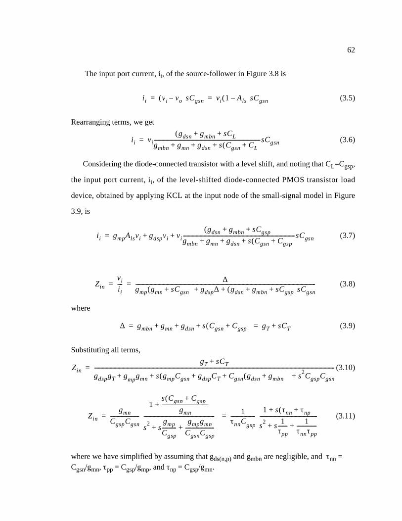
62
The input port current, ii, of the source-follower in Figure 3.8 is
(3.5)
Rearranging terms, we get
(3.6)
Considering the diode-connected transistor with a level shift, and noting that CL=Cgsp,
the input port current, ii, of the level-shifted diode-connected PMOS transistor load
device, obtained by applying KCL at the input node of the small-signal model in Figure
3.9, is
(3.7)
(3.8)
where
(3.9)
Substituting all terms,
(3.10)
(3.11)
where we have simplified by assuming that gds(n,p) and gmbn are negligible, and τnn = Cgsn/gmn, τpp = Cgsp/gmp, and τnp = Cgsp/gmn.
ii vi vo–( )sCgsn vi 1 Als–( )sCgsn= =
ii vigdsn gmbn sCL+ +( )
gmbn gmn gdsn s Cgsn CL+( )+ + +---------------------------------------------------------------------------------sCgsn=
ii gmpAlsvi gdspvi vi+ +gdsn gmbn sCgsp+ +( )
gmbn gmn gdsn s Cgsn Cgsp+( )+ + +-------------------------------------------------------------------------------------sCgsn=
Zinvi
ii---- ∆
gmp gmn sCgsn+( ) gdsp∆ gdsn gmbn sCgsp+ +( )sCgsn+ +-----------------------------------------------------------------------------------------------------------------------------------------= =
∆ gmbn gmn gdsn s Cgsn Cgsp+( )+ + + gT sCT+= =
ZingT sCT+
gdspgT g+ mpgmn s gmpCgsn gdspCT Cgsn gdsn gmbn+( )+ +( )+ s2CgspCgsn+---------------------------------------------------------------------------------------------------------------------------------------------------------------------------------------=
Zingmn
CgspCgsn----------------------
1s Cgsn Cgsp+( )
gmn-----------------------------------+
s2 sgmp
Cgsp-----------
gmpgmn
CgsnCgsp----------------------+ +
------------------------------------------------------
1τnnCgsp-------------------
1 s τnn τnp+( )+
s2 s 1τpp------- 1
τnnτpp---------------+ +
--------------------------------------------
= =

63
It can be seen that the level-shifted diode-connected PMOS transistor is a second-
order system with a zero at ωz=1/(τnn+τnp). The second-order equation in the denominator
corresponds to a second-order system’s characteristic equation2 where
and .
This second-order transfer function allows us to use this load device to peak the output
response and improve the bandwidth of flip-flops and amplifiers. The significant
advantage of the level-shifted diode-connected load device is that the PMOS transistor is
smaller than if the level-shift were absent for large currents, and with a further
modification, can be used advantageously in amplifiers to get large output-signal swings
for lower power dissipations than with regular diode-connected loads.
Biased level-shift circuits have a good turn-on transient, but they suffer from a poor
turn-off transient due to the fact there is no active pull-down circuit [172]. This can be
solved advantageously in the differential case by using the output of the opposite polarity
2. s2 2ξωns ωn2+ +
ωn1
τnnτpp---------------= ξ 1
2---
τnn
τpp-------=
Figure 3.10: Schematic and symbol of Active Pull-down Level-Shift Diode-con-nected (APLSD) PMOS transistor loads in differential circuits.
+ -+ -

64
to drive the gate of the current source. The level-shift circuit in effect becomes an NMOS
inverter with active drives for both transistors as shown in the shaded areas in Figure 3.10,
which we shall call Active Pulldown Level Shift Diode-connected (APLSD) PMOS
transistor loads.
3.4 Flip-Flop Circuit
Synchronous flip-flops3 form an essential and integral component of logic circuits.
Differential flip-flop circuit topologies that are used in non-CMOS process technologies
which include Si BJTs, GaAs MESFET [75][84] and other high-speed process
technologies, have significantly more transistors than conventional static flip-fops or
clocked single- or multi-phase flip-flops in CMOS process technology. The differential
configuration offers all the advantages of a differential circuit which are essential to
optimal high-frequency operation with respect to considerations of noise (power-supply
and substrate noise), crosstalk immunity, common-mode voltage variation immunity and
reduced voltage-swing operation. High-frequency divider circuits in sub-micron CMOS
process technologies employ non-differential complementary operation [79] due to the
fact that the devices are velocity saturated for most of their operation and can have fewer
devices than needed for flip-flops, because dividers only deal with a subset of the input
conditions of a general flip-flop. High-speed divider circuits may also be realized using a
mixer, low-pass filter, and amplifier with inductive loads [83].
Figure 3.11 shows the schematic of a conventional differential master-slave flip-flop
implemented in GaAs MESFET process technology. The same topology carries over to
Si/SiGe BJT, AlGaAs/GaAs HBT, InP/InGaAs HBT or AlGaAs/GaAs HEMT process
technologies with the replacement of the MESFET by the appropriate device. Z1 and Z2
3. Clocked flip-flops are referred to as synchronous flip-flops as opposed to set-reset flip-flops.

65
are load impedances, and could be passive resistors, series combinations of resistor and
inductor, or active devices which realize a series combination of resistance and
inductance, depending on the technology. The differential pair M1-M2 reads data in when
CLK+ is high. The data is stored in the cross-coupled pair M3-M4 when CLK+ goes low
(CLK- goes high). The level-shift circuits M8-M10-M12 and M9-M11-M13 shift the latch
output-voltage down to the voltage range of the input stage of the succeeding latch.
Implementing M5-M6 as a differential pair by connecting their sources to a tail-current
sink keeps the devices in the optimum operating region (saturation in FETs) during circuit
operation.
Flip-flop circuits using single-ended data and clock techniques [88] or differential-
data, single-ended clock techniques [89] are not suitable for parallel data link interface ICs
at Gb/s data rates. The problem is not that the circuits cannot operate at these data rates.
Huang and Rogenmooser [90] report a dual-modulus 64/65 prescaler at 1.65 GHz in
CLK+CLK-
D+
D-
Figure 3.11: Schematic of high-speed differential master slave flip-flop in exotic process technologies such as Si/SiGe BJT, GaAs MESFET, InP/InGaAs HBT or AlGaAs/GaAs HEMT.
M1
M2
M3
M4
M5 M6Q-
Q+
Vbias
M7
M8
M10
M12
M9
M11
M13
master slave
Z1
Z2

66
1.2 µm CMOS process technology using techniques in [88]. Circuit techniques as in [88]
and [89] operate with high slew-rate single-phase clocks. This places severe constraints on
the clock distribution, with corresponding increases in power consumption, decoupling
requirements on the on-chip power supply, and increased power supply [93] and noise
generation. Moreover, the circuit performance is very sensitive to the clock signal rise-
and fall-times [92]. Differential-data single-ended clock flip-flops proposed in [89] suffer
from poor logic-level zero in the presence of glitches on data inputs [91]. Differential-data
and -clock flip-flops used in Si BJT, GaAs MESFET and other advanced process
technologies can operate at higher frequencies with sine-wave differential clocks because
of the low-swing differential nature of the circuit, which does not require that the clocked
transistors be completely switched off. The disadvantage of these circuits is that the
amount of standby current is directly proportional to the transconductance gm, of the
devices, which does not make them competitive in low-frequency applications.
These considerations force the choice of a differential-data and -clock flip-flop
topology. A flip-flop schematic and symbol composed of master-slave cross-coupled
differential latches is shown in Figure 3.12. This flip-flop configuration is a modified
version of a commonly used topology in GaAs MESFET ICs [65] where the clocked
transistors M5, M6 and M13, M14 form differential pairs. Murata et al. [75] suggest a
modification to the basic topology to increase the operating frequency at the expense of
operating range by reducing the current flowing in the cross-coupled pair in the master
and slave latches, making the flip-flop “more dynamic”. These topologies also employ
source followers to level shift the latch output so that the output voltage excursion is
advantageously placed in the center of the common-mode voltage range of the input stage
of the succeeding stage. This allows each stage to be optimally biased for the highest
possible operating frequency and enables a stacking of three transistors.

67
It is not possible to effectively exploit this in CMOS technology because of the
inefficiency of a source follower, which capacitively loads the previous stage and
attenuates the signal output at the expense of power consumption. Additionally, the
stacking of transistors incurs the impact of the body-effect in CMOS which is not the case
in GaAs MESFETs. Therefore, the sources of transistors M5, M6, M13 and M14 in Figure
3.14 are connected to ground. It is desirable from the system-level perspective of testing
and graceful link-performance degradation to have a broadband link. This means that the
flip-flops operate from very low frequencies (10s of MHz) to very high frequencies (up to
one-third the unity current-gain frequency, fT, of the transistor in saturation). This
requirement precludes the adoption of the technique of making the latches more dynamic
to increase their maximum operating frequency at the expense of operating range. The
clock signal is assumed to be a large signal which moves the clocked transistors from
cutoff to saturation. These clocked transistors function as clocked tail-current sinks for the
differential pairs composed of M1-M2 and M9-M10 and the cross-coupled pairs
composed of M3-M4 and M11-M12.
Figure 3.12: Schematic and symbol of high-performance CMOS differential master slave flip-flop. Load devices correspond to those in Figure 3.10.
clk+ clk-
HSDFF
+-
Q+,Q-D+,D-
CLK+CLK-
D+
D-
M1
M2
M3
M4
M5 M6
M9
M10
M11
M12
M13 M14
Q+
Q-

68
The behavior of the flip-flop in Figure 3.12 is described in Figure 3.13. During the
high phase of the clock (when CLK+ is high), the input stage of the master (M1-M2, M5)
reads in the input data. When CLK+ goes low, this value is stored in the cross-coupled
pair M3-M4 and is read at the same time by the input pair of the slave latch formed by
M9-M10. The output of the flip-flop is the latched value at this point in time. In essence,
the flip-flop so described latches the input at the falling edge of CLK+ and the output is
stable from the falling edge of CLK+ to the next falling edge of CLK+. These flip-flops
have sub-150 ps set-up time and zero hold time in 0.5 µm CMOS process technology.
The circuit layout is such that differential pairs are in close proximity and use an
interleaved layout style [61] to minimize offset voltage problems. All differential pairs are
laid out with the same orientation for maximum matching. Layout techniques are used to
ensure that parasitic capacitance and coupling capacitance is minimized. Figure 3.14 (a)
and (b) show the measured output eye-diagram and the output jitter (9 ps rms (58 ps peak-
to-peak)) respectively, corresponding to 3.2 Gb/s operation with 231 - 1 NRZ PRBS input
data patterns at a BER < 10-13, of the flip-flop in Figure 3.12, which was ported to the 0.35
µm CMOS technology by shrinking the 0.5 µm CMOS layout from λ = 0.3 µm to λ = 0.2
µm using the SCMOS_SUBM design rules from the MOSIS service. The input signal
Figure 3.13: Waveforms describing behavior of differential flip-flop in Figure 3.12.
inputlatchedinto masterat falling edge latched data
available at outputat rising edge of clockof clock
Inputdata D+
Clock
Ouputdata
CLK+
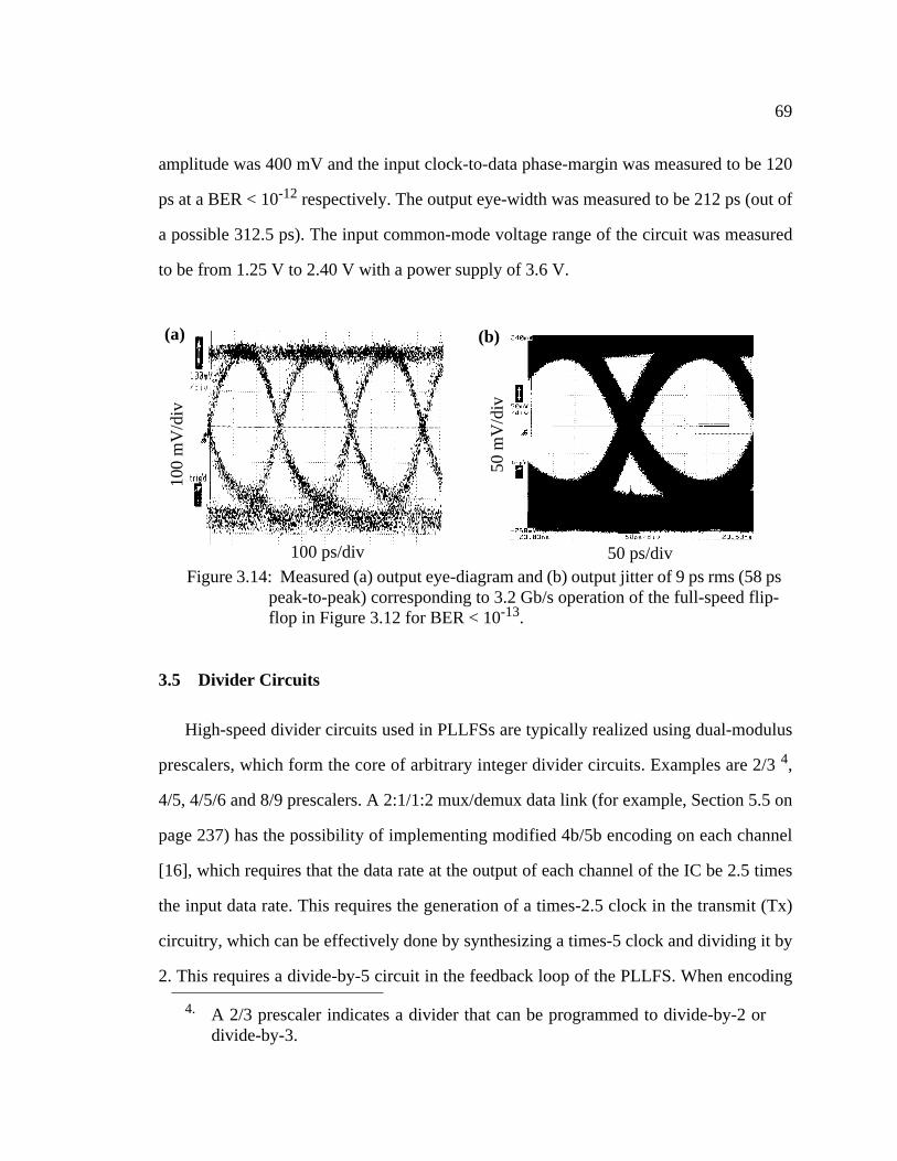
69
amplitude was 400 mV and the input clock-to-data phase-margin was measured to be 120
ps at a BER < 10-12 respectively. The output eye-width was measured to be 212 ps (out of
a possible 312.5 ps). The input common-mode voltage range of the circuit was measured
to be from 1.25 V to 2.40 V with a power supply of 3.6 V.
3.5 Divider Circuits
High-speed divider circuits used in PLLFSs are typically realized using dual-modulus
prescalers, which form the core of arbitrary integer divider circuits. Examples are 2/3 4,
4/5, 4/5/6 and 8/9 prescalers. A 2:1/1:2 mux/demux data link (for example, Section 5.5 on
page 237) has the possibility of implementing modified 4b/5b encoding on each channel
[16], which requires that the data rate at the output of each channel of the IC be 2.5 times
the input data rate. This requires the generation of a times-2.5 clock in the transmit (Tx)
circuitry, which can be effectively done by synthesizing a times-5 clock and dividing it by
2. This requires a divide-by-5 circuit in the feedback loop of the PLLFS. When encoding
4. A 2/3 prescaler indicates a divider that can be programmed to divide-by-2 ordivide-by-3.
Figure 3.14: Measured (a) output eye-diagram and (b) output jitter of 9 ps rms (58 ps peak-to-peak) corresponding to 3.2 Gb/s operation of the full-speed flip-flop in Figure 3.12 for BER < 10-13.
50 ps/div100 ps/div
50 m
V/d
iv
100
mV
/div
(a) (b)

70
is turned off in the link, the PLLFS should produce a times-4 clock, requiring a divide-by-
4 circuit in the feedback loop of the PLLFS. A modified 4b/5b as in [16] requires a divide-
by-2.5 which generates a 50% duty cycle clock in the receive circuit to decode and
demultiplex the received data. A divide-by-2.5 can be generated by NAND logic
operating on the outputs of a 5-bit shift register, two of which are the outputs of D flip-
flops while the last is the output of the master latch of the third flip-flop (which is 90°
behind the second output). This requires a NAND gate that can deliver robust performance
up to 2.5 Gb/s in 0.5 µm CMOS process technology. The jitter performance of this circuit
at high-frequencies is questionable due to Inter-Symbol Interference (ISI) and amplitude
noise problems associated with the output of the NAND gate. A differential NAND gate is
a two level structure, which requires that the D flip-flops be designed to produce different
output levels as they can drive different ports of the NAND gate. This design requirement
adversely impacts the performance of the shift register circuit which is nominally clocked
at 1.25 GHz. These considerations force us to entertain the possibility of a PLLFS at the
receive side which has a times-2 PLLFS following a divide-by-5 circuit. An alternative is
to use a 4b/6b encoding method on the data, which requires a 4/6 prescaler on the transmit
side PLLFS, requiring a divide-by-3 circuit in the receive side which can be done without
a PLLFS.
The design challenges in high-speed divider design are operation at maximum VCO
frequency, low phase-noise, low-supply and -substrate noise generation, supply and
substrate noise immunity, low-power consumption, and small area. Like most Radio
Frequency (RF) circuits, these building blocks have been built in the past using GaAs
MESFET, Si/SiGe BJT and other advanced process technologies, which are now being
supplanted by CMOS process technology. Si/SiGe BJT designs are fast and power
efficient. Recent publications have reported a 2 GHz 6 mW BiCMOS frequency
synthesizer [163] and a sub-1 mA 1.5 GHz dual-modulus prescaler [162] in Si BJT

71
process technology. Traditional RF techniques of fully-differential circuits are employed
in both cases. Additionally, the relatively large supply voltages and the small Vbe of Si
BJT process technology allows series-gating or vertical cascading of circuits for current
re-use, and hence savings in power consumption. Logic gates like NAND gates and flip-
flops can be advantageously merged [163] for faster operation and lower power
consumption. In finer geometry CMOS process technologies, shrinking power supply
voltages imply that the stacking of transistors is limited to three transistors between supply
and ground. Folding of stages is not an attractive option because the PMOS transistor in
finer geometry CMOS process technologies usually has a transconductance less than a
third that of the NMOS transistor in the same process technology, resulting in large PMOS
transistors, whose gate capacitance loads the output of the stage driving the PMOS
transistors.
Implementation of frequency divider circuits in CMOS have focused on using single-
ended dynamic circuits to achieve multi-GigaHertz operation [159][161]. An alternative
implementation [160] exploits the idea of switching between the quadrature signals of a
synchronous divide-by-4 circuit (the outputs of the master and slave latch of the flip-flop
whose output is the divide-by-4 signal) using an analog phase-selection circuit to achieve
a 4/5 prescaler. This eliminates the speed and power penalty due to the presence of a logic
gate (usually a NAND gate) in the critical feedback path of traditional prescalers. The
dividers are implemented as ripple counters. Division by cascading may not be
advantageous in the case of data links because the synthesized clock frequency is used to
multiplex and demultiplex the input at 1/Nth the data rate. Since the synthesized clock
frequency is used to retime the input data after division, there might be some complexity
in the retiming circuitry because of the uncertainty in the phase relationship between the
VCO output in a PLLFS and the output of the dividers when the dividers are cascaded
instead of being operated as synchronous dividers.

72
m/n prescaler cores are implemented by a shift-register circuit with log2(n) flip-flops
that implement a counter state-diagram which cyclically shifts through m or n states
depending on a control signal. These circuits usually do not require a reset signal, because
they fall into the counter state-cycle irrespective of whichever state they start from. They
are usually synchronous circuits which means that they are clocked at the highest clock
frequency, consume the most power and occupy the largest area in the divider chain.
In Figure 3.15, if 4/5 prescaler control signal, M1, is equal to logic low (“0”), the
output of FF3 is always at logic high (“1”), which means that the NAND gate at the input
of FF1 acts as an inverter. In this case, the 4/5 prescaler functions as a divide-by-4 circuit
because of the net inversion around the loop formed by FF1 and FF2. Starting from any
state, FF1 and FF2 cycle through 00 -> 10 -> 11 -> 01 -> 00 ->..., as shown by the state
diagram in Figure 3.16 (a), where the first bit represents the state of FF1 and the second
bit, the state of FF2. When M1=1, the shift register loop is closed over three flip-flops and
the shift register sequence is 100 -> 110 -> 111 -> 011 -> 001 -> 100 -> 110 ->....., where
bit i is the state of flip-flop FFi in Figure 3.15. If the 4/5 prescaler starts from 000, it goes
to 100, from 010 it goes to 101 and then to 110. This describes all possible states of the 4/5
prescaler.
D Q
Q
D Q D QQ Q
M1
outputFigure 3.15: Schematic of 4/5 prescaler. M1 is the 4/5 control bit.
FF1 FF2 FF3
φosc

73
Figure 3.17 shows the schematic of the 4/5/6 prescaler. Setting the control signals M1
to logic low and M2 to logic high configures the 4/5/6 prescaler as a divide-by-4 circuit, as
in the case of the 4/5 prescaler. Setting both M1 and M2 to logic high configures the 4/5/6
prescaler as a divide-by-5 circuit, which functions in the same way as the 4/5 prescaler in
divide-by-5 mode, with the additional delay of the second NAND gate, which is
controlled by M2 at the input of FF1. When M1 is set to logic high and M2 is set to logic
low, the 4/5/6 prescaler is configured as a divide-by-6 circuit, effectively implementing
the circuit schematic in Figure 3.18 (a). The state diagram of this circuit has two
independent cycles, indicating that it could function either as a divide-by-6 or as a divide-
by-2 circuit when M1 is set to logic high and M2 is set to logic low on power-up.
02
5
6
4
73
1
3
2
1
0
Figure 3.16: State diagram of the 4/5 prescaler in (a) divide-by-4 and (b) divide-by-5 operation.
(a) (b)
D Q
Q
D Q D QQ Q
M1
output
Figure 3.17: Schematic of the 4/5/6 prescaler. M1, M2 are the 4/5/6 control signals.
FF1 FF2 FF3
M2φosc

74
The circuit schematic of a 4/6 prescaler is shown in Figure 3.19, where a mux is used
to switch between the divide-by-4 and the divide-by-6 modes by setting M1 to logic low
and logic high respectively. A reset circuit is required for the case of the divide-by-6 to
force the state diagram into the cyclic six-state diagram in Figure 3.18 (b), to implement a
divide-by-6 circuit instead of a divide-by-2 circuit.
Noise in divider circuits is a significant concern in as much as they generate power-
supply and substrate noise. Prescaler noise considerations are discussed in [164], [165],
[166], [167], [168] and [169]. Phase-noise at the input of an ideal digital divide-by-N
circuit is reduced by a factor of N at the divider output. Real dividers add their own phase-
noise to the output. When the divider is implemented as a synchronous counter, the phase-
noise at the divider output is given by [171]
D Q
Q
D Q D QQ Q
output
Figure 3.18: Schematic of 4/5/6 prescaler in divide-by-6 mode and its associ-ated state diagram.
FF1 FF2 FF3 02
56
4
73
1φosc
(a) (b)
D Q
Q
D Q D QQ Q
output
Figure 3.19: Schematic of 4/6 prescaler. M1 selects the mux between divide-by-4 and divide-by-6 modes.
FF1 FF2 FF3
φosc
Μ1

75
(3.12)
where N is the division ratio and Sφ,add(f) is the additive noise of the divider.
In a divider implemented as a ripple counter, each stage independently contributes its
noise components to its output, making the noise at the divider output higher than that for
a synchronous counter [134]. Power-supply and substrate noise act as noise sources that
are added to the output of each divider stage. The feedback division action in a PLLFS
results in noise components that are far removed in frequency to be aliased to within the
input reference frequency of the Phase Frequency Detector (PFD). Dividers need to
designed so that their sensitivity to substrate and power-supply noise is minimal, which
effectively means that they have a low output-impedance in the case of voltage-mode
dividers. Since synchronous counters add less additive noise to the divider output than
asynchronous counters, it is better to have synchronous counters than asynchronous
counters, trading noise performance for power consumption. Noise added by each divider
stage can be reduced by fully differential divider design with level-shift diode-connected
loads for large SNR and low sensitivity to power-supply and substrate noise.
3.5.1 Prescaler Design
The design requirement of a 2.5 Gb/s half-speed data link requires a VCO that is
capable of delivering 1.7 GHz performance so that the PLLFS can lock onto the
synthesized 1.25 GHz, which is comfortably below the maximum frequency of the VCO
by 20%. This design margin allows the PLLFS to tolerate larger input phase-noise while
still maintaining lock than it would if the PLLFS had been trying to lock to a frequency of
the VCO near the top or bottom end of its operating range. This design requirement means
SΦout f( )Sφin f( )
N2--------------- Sφ add, f( )+=

76
that the prescalers which operate in the feedback loop of the PLLFS need to be operational
up to a frequency of at least 1.7 GHz.
The prescaler designs outlined in Figure 3.15, Figure 3.17, and Figure 3.19 require a
NAND gate and a mux that are capable of operating at 2 Gb/s. In addition, the NAND gate
or the mux which drives FF1 should be merged into the master latch of FF1 so that the
latency of the gate is partially hidden by the latency of the master latch.
High-speed differential flip-flop design was discussed in Section 3.4 on page 64. The
design requirements of the prescaler divider force us to re-evaluate the design because of
the increased frequency of operation and the required low impedance nature of the load
devices. The differential flip-flop described earlier requires large input-swing signals on
the clocked transistors in order to switch them on and off. These clock signals were
generated by local inverters in that design. This is not an attractive option at these
frequencies because of the power-supply and substrate noise generated by the inverter
circuits. An effective strategy to design high-speed D flip-flops is to
• Design for a low-swing differential clock
• Design for a low-capacitance, low-impedance load
The clock distribution circuit should behave as a voltage source (low impedance
output) so that it can charge and discharge the parasitic capacitances associated with the
load with a small time-constant. The choice of a low-swing differential clock driver that
delivers a clock whose amplitude is between 0 V and 1 V is difficult to achieve with an
active NMOS stage design. The use of PMOS transistors in the amplifier gain path is sub-
optimal because of their low transconductance. A differential amplifier driving a source
follower with active current-sink bias can deliver a differential clock whose amplitude is
between 0.8 V and 2.0 V, and whose output looks like a voltage source. The design of the
clock amplifier/buffer will be discussed later. The output voltage swing of the optimal

77
clock buffer design will not completely switch off the clocked transistors that are
supposed to be off, when the clock goes low in the differential flip-flops designed earlier.
The flip-flop schematic that best accommodates the clock buffer described in the
previous paragraph, is shown in Figure 3.12, where the threshold voltage of the clocked
NMOS transistors have been increased so that they are turned off by a clock which swings
between 1.0 V and 2.0 V. At the high-end of the operating region, the clock buffer can
swing between 1.0 V and 2.0 V due to capacitive loading and data-to-clock coupling in the
flip-flops. The symbol for the APLSD PMOS transistor load has the cross-coupled pull-
down connection implicit in its symbol. The threshold adjustment for the clocked
transistors M5, M6, M13 and M14 is achieved by converting them to differential pairs as
shown in Figure 3.20. The transistors M15 and M16 operate in the triode region and are
sized to operate with a drain-to-source voltage of 0.3 V. Since the shaded differential pairs
perform distinct functions of read and latch, they are connected as shown in Figure 3.20.
CLK+
CLK-
D+
D-
Figure 3.20: Schematic and symbol of differential master slave flip-flop
M1
M2
M3
M4
M5 M6
M9
M10
M11
M12
M13M14
M15 M16
Q+
Q-
bias bias

78
This relaxes the design requirement on the latch output voltage-swing to switch the cross-
coupled pairs M3-M4 and M11-M12. Otherwise, the cross-coupled pair slows down the
operation of the read circuit at high-frequencies when the current sink transistors M6 and
M14 are not fully turned off. Separating the differential pairs allows the currents in the
latch circuits to be set differently from the read differential pair [75]. In the design case
considered here, this allows the cross-coupled pairs M3-M4 and M11-M12 to have less
current than the read differential pairs M1-M2 and M9-M10 and hence lower negative
resistance to compensate for the fact that their gate-to-source voltage is higher. This yields
greater performance improvements when the differential pair M1-M2 is replaced by a
two-transistor-tall differential-pair stack when logic is merged into the first stage,
reducing the output swing of the read-differential stage. This approach is also helped by
the fact the APLSD PMOS transistor loads enable larger output voltage-swings than
simple diode-connected or level-shift diode-connected PMOS transistor loads. The reason
for connecting M5 and M13 as a differential pair as opposed to M5 and M6 as a
differential pair pursued in [75] does not hold here because we desire a broadband high-
frequency flip-flop. The differential outputs of the flip-flop (Q+ and Q-) directly drive the
next stage because of the advantage of the large output voltage-swing offered by the
APLSD PMOS transistor loads. The flip-flop, as designed for 2.0 GHz operation,
consumes 6.3 mA of current from a 3.6 V supply, and occupies an area of 106.8 µm x
214.8 µm in 0.5 µm CMOS process technology, using the MOSIS Scalable CMOS Sub-
Micron (SCMOS_SUBM) design rules. The flip-flop has 154 drawn devices and is laid
out in a fully differential fashion so that the parasitic capacitances are exactly equal on
differential nodes as shown in Figure 3.21. The bias generation circuitry for transistors
M15 and M16 in Figure 3.12, is local as shown in Figure 3.21. The bias voltage is
decoupled with local decoupling-capacitors made from NMOS transistor gates, whose
drain, source, and bulk tied together to the local ground (GND) in Figure 3.21. Power

79
(Vdd) and ground connections can run over the flip-flop in third level metal. Power-
supply decoupling capacitors are laid out on both sides of the flip-flop which provide the
ground connection by construction. Second-level metal or third-level metal wires connect
the power of the flip-flop to the power of the decoupling capacitors.
DIN DOUT
CLOCK
Figure 3.21: Layout of 1.6 GHz D flip-flop for prescaler.
MA
STE
R
RE
AD
MA
STE
R
LATC
H LO
AD SLAVE
BIA
S
GND GND
GND GND
VDD
Figure 3.22: 1.25 Gb/s data flip-flop with 52 drawn devices occupying an area of 58.2 µm x 69 µm.
DIN
CLOCK
DOUT
Q+
Q-
APLSDLOAD
MA
STE
R
RE
AD
MA
STE
R
LATC
H SLAVE
VDD
GND

80
The layout in Figure 3.21 can be modified for a lower frequency D flip-flop, whose
schematic is shown in Figure 3.12. For example, a 1.25 Gb/s D flip-flop layout is shown in
Figure 3.22, which occupies an area of 58.2 µm x 69 µm and has 52 drawn devices. This
flip-flop utilizes the APLSD PMOS transistor loads, but does not implement the
transistors M15 and M16 in Figure 3.20, as the clock waveform is of sufficient amplitude
(0.8 V to 2.2 V) to switch the clocked transistors. In the layouts shown in Figure 3.21 and
Figure 3.22, the slave latch is larger than the master latch, because it drives a larger
capacitive load.
Rx
Rx
TxDFF BUF
BUF
To VTT=1.55Vthrough 50Ω.
Data
Clock
Figure 3.23: Schematic of layout to test operation of D flip-flop in Figure 3.20.
30 mW
30 mW
22 mW 60mW
60 mW
39mW
Figure 3.24: Setup time for D flip-flop in Figure 3.21 at 2 GHz. Hold time is -20 ps.
160 ps
Data Input
Clock input
latching clock edge
(b)
130 ps
Data Input
Clock input
latching clock edge
(a)

81
The performance of the D flip-flop shown in Figure 3.21 is tested using the 0.5 µm
CMOS layout of the schematic shown in Figure 3.23. Fully differential data and clock
with 100 ps rise- and fall-times are supplied at LVDS levels to the D flip-flop through
electrical LVDS receivers. The output of the D flip-flop feeds a Transmit (Tx) circuit
through a buffer. The extracted netlist of the layout is simulated with the slow process
corner libraries at a junction temperature of 80 °C.
Figure 3.24 shows the simulated setup time for (a) 2 GHz and (b) 2.3 GHz operation.
The setup time at 2.0 GHz is 130 ps, which increases to 160 ps at 2.3 GHz due to the
reduced swing of the clock signal. The hold time according to the simulations is -20 ps,
that is, the data could change 20 ps before the latching clock falling edge. The transient
waveforms of the schematic in Figure 3.23 at the setup time of 160 ps in Figure 3.24 (b) is
shown in Figure 3.25. The top panel shows the input data to the flip-flop, with the latching
clock waveform shown in the middle panel. The output of the flip-flop, which is shown in
InputData
LatchingClock
OutputDatainto 50Ω
Figure 3.25: D flip-flop (Figure 3.12) operation at 2.3 Gb/s at 160 ps clock-to-data setup time.

82
the bottom panel in Figure 3.25, is seen to be identical to the input waveform in the top
panel, which demonstrates the correct operation of the flip-flop at 2.3 Gb/s. Single-ended
waveforms are shown for clarity. Note that the amplitude of the clock is 630 mV.
3.5.2 High-Speed Differential Logic Gates
Differential logic gates in ECL or CML employ series-gated logic circuits with
vertically stacked differential pairs. The advantage of vertically stacking gates is that the
bias currents can be reused to reduce power consumption of the gates. The vertical
stacking is limited by the voltage headroom that is available due to the power supply and
the technology that is being used. We start with the basic configuration of a differential
multiplexer in Figure 3.26 with APLSD load devices. When the signal s- is high and s+ is
low, the input differential signal D1+ and D1- is available at the output. The differential
input D2+ and D2- are available at the output when s- is low and s+ is high. This action
can be described by the boolean logic equation
(3.13)
M2 M3
M4 M5 M6 M7D1- D1+ D2- D2+
s- s+
bias
Figure 3.26: Schematic of differential 2:1 multiplexer
OUT-OUT+
M1
OUT S D1⋅ S D2⋅+=

83
When S is replaced by D1, and D2 is replaced by the negation of D1 in Equation 3.13,
we get the logic operation of an eXclusive-OR (XOR) gate. Negation in differential logic
is trivially obtained by interchanging the polarity of the pair of signal wires that represent
a signal.
(3.14)
To implement an AND/NAND gate, we note that for the logic expression OUT = S •
D, OUT is equal to logic zero whenever one of the inputs, say S, is equal to logic zero.
OUT is equal to D when S is equal to logic one. Using these observations, we remove
transistors M6 and M17 in Figure 3.26 to get the differential AND/NAND gate in Figure
3.27. The operation of the gate is as follows: AND is high only when S = D = logic 1, and
NAND is low only when S = D = logic 1. It is to be noted that the output labeled AND is
faster than the output labeled NAND because of one less series-gated transistor in the path
to the output labeled AND. The capacitance at the output labeled AND is higher because
of the two circuit paths connected to it, making the source diffusion and channel
OUT D1 D2⋅ D1 D2⋅+ D1 D2⊕= =
M2 M3
M4 M5D+ D-
S+ S-
bias
Figure 3.27: Schematic of differential AND/NAND gate.
ANDNAND
M1

84
capacitances of transistors M3 and M5 visible at the output labeled AND in Figure 3.27,
depending on the logic level of the signals driving the gates of transistors M3 and M5.
To increase the delay of the signal path through M3 when S- goes high, we add the
differential input pair M6-M7 as shown in Figure 3.28, whose outputs are connected to the
AND output. This is a logic no-operation, but results in the same signal paths seen from
the inputs at the lower input differential pair driven by S+ and S- to the outputs. The
parasitic capacitance at the AND and NAND outputs are only approximately equal. To
equalize the parasitic capacitance at the NAND output, we add the dummy transistors M8
and M9 which are connected to a bias voltage Vb, as shown in Figure 3.28. Vb is set to the
common-mode voltage of input signal D. During operation, the AND output sees more
transient capacitance than the NAND output, due to the inability of transistor pair M8-M9
to accurately mimic the transient capacitance seen at the AND output for different values
of input D and S. Therefore, we add about 40 fF of gate capacitance using transistor M10
to approximately balance the output slew rates of the NAND and AND outputs. The
voltage levels of the signal S are set to be between 0.8 V and 2.4 V while that of signal D
is between 2.0 V and 3.4 V. Simulations of the AND/NAND gate at 85 °C and 3.6 V
M3M2
M7M6M5M4D+D-D+
S+S+
bias
Figure 3.28: Schematic of balanced differential AND/NAND gate.
NAND AND
VbM9M8
M1
M10

85
power supply, with the slow process corner libraries of the 0.5 µm HP-CMOS14TB
process, indicate that it can operate at 2.0 G/s. The output voltage swings between 2.8 V
and 3.6 V due to the vertical stack of three NMOS transistors. This makes a level-shift
circuit necessary in order to drive a single-stack differential amplifier, flip-flop, or logic
gate, whose input common-mode voltage is around 1.8 V.
A differential NOR gate is obtained from an AND gate by using inverted inputs
instead of true inputs. Accordingly, if inputs S and D are replaced by their complements in
Figure 3.27, we get a NOR gate with the output labeled NAND being the OR output and
the output labeled AND being the NOR output.
.
High-speed logic operations are usually pipelined with a latch or flip-flop following
the combinational logic gate. The speed of operation of such a structure is limited by the
sum of the delays of the combinational gate and the delay of the latch. This can be reduced
Figure 3.29: Schematic of differential master slave flip-flop with merged mux in master latch.
D1- D1+
CLK+
CLK-
S+
S-
M1
M2
M3
M4
M5 M6
M9
M10
M11
M12
M13M14
M15 M16
Q+
Q-D2- D2+
M7a M8a
M7b M8b
bias bias

86
if we can merge the combinational gate and the latch. The speed of operation of the 4/6
prescaler in Figure 3.19 is limited by the delay of the mux plus the delay of the master
latch in the right-most flip-flop. We replace the input differential pair M1-M2 in the
master slave flip-flop in Figure 3.20 by the vertical stack of differential pairs M2-M7 in
Figure 3.26 (corresponding to M1, M2, M7a,M8a, M7b and M8b in Figure 3.29), to get
the merged mux flip-flop in Figure 3.29. A merged NAND flip-flop is created in a similar
manner and used in the 4/5 prescaler in Figure 3.15 and in the 4/5/6 prescaler in Figure
3.17.
3.5.3 Prescaler measurements
The prescaler designs in Figure 3.15 (4/5 prescaler), Figure 3.17 (4/5/6 prescaler) and
Figure 3.19 (4/6 prescaler) are designed to run at 1.6 GHz at a junction temperature of
85 °C using the slow process corner model decks of the 0.5 µm HP-CMOS14TB process.
The die photograph of the testdie (T7) to measure the performance of the 4/5, 4/5/6 and
4/6 prescalers, is shown in Figure 3.30. The testdie T7 is designed so that a high-speed
differential clock signal can be brought into the IC from an external source like a Bit Error
Ratio Tester (BERT), using the receiver circuit called Rx, as shown in the die photograph
in Figure 3.30. The output of the clock receiver drives three clock buffers, which in turn
drive the prescalers. The output of each divider is observed using electrical LVDS
transmitters which are capable of operating at a data rate of 3.0 Gb/s. The output of each
prescaler is buffered prior to driving the LVDS transmitter. The LVDS transmitters are
laid out in an array and have their power supplies isolated by bond-wires from the
prescaler power supplies. Noise generation circuitry is included on the IC in the form of
two single-ended current-starved tunable VCOs driving on-chip digital TTL pads. The
power supply of the noise generation circuitry is directly connected to the power and
ground nodes of the clock receiver, clock buffer, and divider circuitry.

87
The noise generation circuitry has two single-ended oscillators with frequency range
from 600 MHz to 950 MHz. One of the oscillators is designed to inject noise into the
ground node and the other into the power node. The latter oscillator was designed to be
non-operational when the ground supply of the oscillator was disconnected. However,
substrate contacts in the oscillator are able to provide the ground connection for the
oscillator. This means that a noise oscillator was always injecting noise into the substrate
and power supply of the circuits being measured. During measurements, the control
voltage of the noise oscillator was set to 0 V.
The prescaler circuitry was laid out using a fully differential layout style, with single
devices split up into multiple devices, to support an interleaved layout style for differential
transistors. All transient waveforms are displayed on the scope after attenuation by 20 dB.
Simultaneous display of the waveforms on the sampling scope is possible because of a
Testdie (T7) to measureperformance of 4/5, 4/5/6and 4/6 prescalers in 0.5 µmCMOS technology. The ICmeasures 2.5 mm x 2 mm.Accounting for the bypassc a p a c i t o r s f o r e a c hprescaler, the 4/5 prescaleroccupies 213 µm x 700 µm,the 4/5/6 prescaler occupies286 µm x 700 µm and the4/6 prescaler occupies 215µm x 7 0 0 µm . E a c hprescaler has an outputbuffer which is 105 µm x273 µm.
Figure 3.30: Die photograph of T7 for measuring prescaler performance.
Noi
seG
ener
atio
nC
ircu
itry
LVD
S T
rans
mitt
er A
rray
(1x6
)
ClockBuffers
Rx
4/5
4/6
4/5/6

88
trigger pattern from the BERT, which has a period of φin/(4*5*6). Waveforms are
displayed in the top-down order of their position in the layout, that is, positive and
negative differential outputs of the 4/5 followed by that of the 4/5/6 and the 4/6 prescaler
outputs respectively. Jitter histograms are measured at the smallest possible manual
timebase setting without attenuating the waveform to remove the slope-error in jitter
histogram measurement. The measured observations on the maximum operating
frequency of the prescalers indicated that the 4/5/6 was the slowest of the three prescalers
by about 100 MHz, that is, it failed at about 100 MHz below the other prescalers in each
mode of operation. No prescaler was found to operate beyond any other prescaler by more
than 200 MHz. Accordingly, their maximum measured operating frequency performance
is reported together as if they all had the same maximum frequency of operation. The
4/5/6 failed earlier than the 4/5 and 4/6 prescalers because it has two cascaded NAND
gates at the input of the first flip-flop (FF1 in Figure 3.17) as opposed to only one gate at
the input of the first flip-flop in the 4/5 and 4/6 prescalers. The 4/5 and 4/6 prescalers have
very close maximum operating frequencies because the NAND gate (Figure 3.15) and the
multiplexer (Figure 3.19) at the input of the first flip-flop are merged into its master latch.
Both merged designs have a stack of four transistors between power and ground.
M2 M1 4/5 4/5/6 4/6
0 0 1/4 (2.16 GHz) NO-OP 1/6 (2.16 GHz)
0 1 1/5 (2.14 GHz) 1/6 (2.14 GHz) 1/4 (2.14 GHz)
1 0 1/4 (2.17 GHz) 1/4 (2.17 GHz) 1/6 (2.17 GHz)
1 1 1/5 (2.10 GHz) 1/5 (2.10 GHz) 1/4 (2.10 GHz)
Table 3.1: Measured maximum frequency of operation of each setting of the
4/5, 4/5/6 and 4/6 prescalers on testdie T7.

89
Table 3.1 summarizes the operation code and maximum measured operating
frequency of each prescaler. Note that M1 and M2 in Table 3.1 correspond to the control
signals in the prescaler schematics in Figure 3.15, Figure 3.17 and Figure 3.19.
The measured self-referenced jitter of the prescalers is approximately constant till 1.5
GHz. There is a small increase in the self-referenced jitter beyond 1.5 GHz. For example,
the self-referenced jitter of the 4/6 prescaler is shown in Figure 3.31. It can be seen that for
most of the operating range, the rms jitter performance of the prescaler is approximately
constant and less than 2.0 ps rms. These measurements include the rms jitter contribution
of the oscilloscope trigger circuit, which is between 1.5 ps and 2.0 ps. Figure 3.32 (a)
shows the transient waveforms of the prescaler outputs corresponding to operation at 2.17
GHz input clock frequency, with mode bits M2 and M1 set to logic high and low
respectively, setting the 4/5 and 4/5/6 prescalers to divide-by-4 mode and the 4/6 prescaler
to divide-by-6 mode respectively. All transient waveforms are attenuated by 20 dB prior
to display on the sampling scope. Figure 3.32 (b), Figure 3.33 (a) and (b) shows the jitter
Figure 3.31: Self-referenced jitter (rms and peak-to-peak) dependence of 4/6 pres-caler on operating frequency.
Operating Frequency (GHz)

90
histogram of the output of each prescaler with respect to the trigger pattern, at the input
frequency of 2.17 GHz, for the 4/5/6, 4/5 and 4/6 prescaler outputs respectively. The rms
jitter of the 4/5, 4/5/6, and 4/6 prescalers at 2.17 GHz was measured to be 2.037, 1.68, and
1.917 ps respectively.
Figure 3.34 (a) shows the operation of the prescalers at 2.16 GHz for M2 and M1
equal to logic low. In this mode, the 4/5/6 prescaler is not operational since the feedback
(a) (b)
Figure 3.32: (a) Prescaler outputs at 2.17 GHz (M2=1,M1=0). 4/5, 4/5/6 prescalers in divide-by-4 mode and 4/6 mode in divide-by-6 mode. (b) shows the jitter histogram of 4/5/6 prescaler output with respect to the trigger pattern.
Figure 3.33: Trigger -pattern referenced (a) 4/5 prescaler jitter of 2.04 ps rms (13.8 ps peak-to-peak) and (b) 4/6 prescaler jitter of 1.92 ps rms (13.3 ps peak-to-peak).
(a) (b)

91
loop (Figure 3.17) is open. The 4/5 and 4/6 prescalers are set to divide-by-4 and divide-by-
5 modes. Figure 3.34 (b) shows the operation of the prescalers at 2.14 GHz for M2 and M1
equal to logic low and high respectively, which sets the 4/5, 4/5/6 and 4/6 prescalers to
divide-by-5, divide-by-6, and divide-by-4 modes respectively.
Setting M2 and M to logic high sets the 4/5, 4/5/6 and 4/6 prescalers to divide-by-5,
divide-by-5 and divide-by-4 modes respectively, as shown in Figure 3.35, at the maximum
operating frequency of 2.1 GHz.
(a) (b)
Figure 3.34: Prescaler outputs at 2.16 GHz for (a) (M2=0, M1=0) and at 2.14 GHz for (b) (M2=0, M1=1). The display order is + and - outputs of 4/5, 4/5/6 and 4/6, after attenuation by 20 dB.
Figure 3.35: Prescaler outputs at 2.1 GHz (M2=1, M1=1). The display order is + and - outputs of 4/5, 4/5/6 and 4/6, after attenuation by 20 dB.

92
3.5.4 Toggle Flip-Flops with RESET
Toggle Flip-Flops (TFFs) are used as frequency dividers in the parallel data link to
generate the demultiplexing signals in the demultiplexer, as well as the master clock for
the digital circuitry in the optional datapath block shown in Figure 3.1. The output stage of
the toggle flip-flop has to drive the demultiplexer circuitry, the succeeding toggle flip-flop
in the toggle flip-flop chain, and is connected back to itself. Therefore, the output drive
signal from the TFFs is isolated from the slave latch output by inverters. The TFF is
obtained from the HSDFF by cross-connecting the outputs to the inputs as shown in
Figure 3.36.
TFFs require a reset signal when they are implemented as part of a demultiplexer in a
parallel link. This is accomplished by using the merged mux flip-flop in Figure 3.29, with
S replaced by reset and D2 replaced by the inverted output of the flip-flop. The
CLK+
CLK-
Q
Figure 3.36: Schematic and symbol of high-speed Toggle Flip-Flop (TFF).
Q
M1
M2
M3
M4
M5 M6
M9
M10
M11
M12
M13 M14
M7
M8
M15
M16
TFF+-
clk-RESET
Q+
Q-clk+
M17
M18
M19RESET
M20
M21
M22
M23

93
modification of the differential input pair M1-M2 into one input of a multiplexer would
require that the input common-mode voltage level be “raised” by the drain-to-source
voltage Vds of the transistor implementing the differential select of the multiplexer. This
would necessitate larger transistor sizes in order to compensate for the body effect. The
additional consequences of this design choice are the increase of the common-mode
voltage of the master latch output, the increase of the common-mode voltage of the output
latch since it feeds back to the master latch input, and the sub-optimal performance of the
cross-coupled pair M3-M4 (which does not turn off completely because of the voltage
excursion range and common-mode voltage range of the master multiplexer stage input
voltage).
An alternative solution is obtained by considering the system level design
considerations pertaining to the RESET signal. We adopt the reset method shown in
Figure 3.36, implemented by transistor M20. The biases of the load transistors of each
output of the latch are separated so that the positive differential output load is biased
differently from the negative differential output. The bias of one of the outputs (in this
case, the positive output) is pulled to ground by turning on M20 with the asynchronous
RESET signal. This drives the corresponding latch output to the positive rail, while the
other output gets discharged to ground by the action of the CLK signal. This method
works well for a single TFF but introduces an uncertainty in subsequent TFFs, which are
connected in a ripple configuration in a divider chain. This is because the output whose
bias transistor gate is not pulled to ground, will not be discharged, because of the absence
of the clock signal from the preceding TFF during the assertion of the RESET signal. This
manifests itself as a situation where, if the state of divider chain of TFFs were viewed as a
bit vector, with the position in the vector corresponding to the order in the divider chain,
the first bit (corresponding to the TFF clocked by the clock signal) will always be 0 after
reset. The other bits can either be 0 or 1 depending on the state of the TFF when the

94
RESET signal was activated and how long it was activated. This results in a large number
of possible sequences of the demultiplexed data outputs corresponding to a single high-
speed input data stream. We find that this problem is solved by an aligner circuit at the
output of each demultiplexer, which must be present in parallel links since the data source
and data sink of the data link can have asynchronous reset signals occurring at different
times. The aligner circuit aligns the output of each 1:N demultiplexer based on the control
information obtained from a symbol delineation signal (typically called a FRAME signal).
This issue is independent of the state of the bit-vector corresponding to the initial state of
the TFF after deassertion of the RESET signal. In the case of a 1:4 demultiplexer, which
operates on a full-speed clocked data stream, and requires the presence of two cascaded
TFFs to derive the half-speed and fourth-speed clocks, the possible initial state induced
deserialized data streams correspond to the same cases accounted for by the different
occurrences of the asynchronous RESET signals at the data source and sink. The
uncertainty in the initial state of the demultiplexer can then be solved by the aligner
circuit, which is a necessary part of the system.
3.6 Slow-speed Logic Circuitry
The choice of a 32 bit datapath (Figure 3.1) imposed by the host-interface bus width
means that the datapath and associated digital circuitry will run at a maximum data rate of
one-fourth the link data rate. Dynamic logic implemented using a single clock-phase
[88][94] technique can be used for digital logic circuitry for operation at frequencies lower
than that which requires differential ECL logic circuits and higher than that which can be
accommodated by static5 CMOS logic styles (pass-transistor logic, double pass-transistor
5. Static refers to a logic style which does not have dynamic nodes, that is, there isalways a path from either supply (power or ground) to any node in the circuit.The architecture using this logic style may or may not have flip-flops or latchesas part of the logic gate.

95
style, Differential Cascode Switch Voltage Logic (DCVSL) etc.). Dynamic circuits are
faster than static circuits because they trade circuit data load for clock load by conditional
charge (discharge) of nodes which are setup to have (not have) charge during a pre-charge
(pre-discharge) phase determined by a sampling signal called the clock. The disadvantage
of this approach is that this is a full-rail logic style like all digital logic styles and requires
a full-rail clock whose rise- and fall-times are critical parameters for proper circuit
operation. This presents the design problem of generating and routing a rail-to-rail single-
phase clock, while at the same time, minimizing the associated power-supply and
substrate noise generation, which is inimical to high-speed low-swing differential circuits.
The advantage of this approach is that the power consumption can be brought down for
low frequency operation because of the absence of the standby current dissipation in
differential low-swing circuits.
Dynamic TSPC [88] flip-flops may be used in the first level of the 4:1 multiplexer and
the last level of the 1:4 demultiplexer to realize these power savings. The rail-to-rail clock
generation and distribution within the high-speed IO circuitry comprising 1:4
demultiplexers, 4:1 multiplexers, HSDFFs, TFFs, Rx, and Tx circuitry, is ameliorated by
generating the rail-to-rail clocks locally within each channel and distributing the clock to
the dynamic circuitry using them. The last TFF in the divider chain generates the
multiplexing and demultiplexing differential fourth-speed (250 MHz) control signals. The
positive output is used to clock the dynamic TSPC flip-flops and the negative output is
used to supply the clock to the subsequent datapath (for example, the nibble align
circuitry) operating on the demultiplexed data.
The schematics of the dynamic flip-flops used are shown in Figure 3.37 (nnpp flip-
flop) and Figure 3.38 (ppnn flip-flop). The name nnpp denotes a flip-flop whose input
flows through during the high-phase of the clock and whose output is latched from falling
edge to falling-edge of the clock signal. The TSPC latches are designed such that the clock

96
transistor load is minimized by connecting only one transistor per latch (n-section in
Figure 3.37) to the clock, followed by another identical latch section. This is in contrast to
the latch in [88], which is composed of a first n-section where the outer transistors are
clocked, and a second n-section identical to the n-section in Figure 3.37. The waveform
drawing on the DFF symbol indicates that the DFF latches on the falling edge of the clock.
The schematic and symbol in Figure 3.37 show an nnpp DFF, which latches on the falling
edge of the clock φ. This DFF is composed of two phase-inverted nn and pp sections,
functioning as the master and slave latches respectively. Figure 3.38 shows a ppnn DFF
whose master latches on the rising edge of the clock φ.
Figure 3.37: Schematic and symbol of an nnpp DFF.
DFF
φ
D Q
φφ φ φ Q
n-section p-section
φφφ φDQ
φ
D QD-FF
Figure 3.38: Schematic and symbol of a ppnn DFF.
p-section n-section

97
3.7 Clock Distribution
This section presents a novel clock distribution scheme to achieve low-skew in high-
speed VLSI systems. The method was devised to solve the problem of distributing a 1.0
GHz clock along a 1.0 Gb/s 10-channel PECL to CMOS interface circuit in 0.8 µm
CMOS. The differential clock signals are distributed along an 1800 µm lossy transmission
line, which is connected between the differential input stage of an amplifier and the diode-
connected load of the differential amplifier with a peak-to-peak swing of approximately
1.0 V, forming a distributed differential amplifier, which is, in effect, the clock
distribution circuitry. Each section has five taps for local clock amplification circuitry.
This scheme results in a simulated skew of less than 20.0 ps across 3600 µm and
consumes 1 W in 0.8 µm CMOS process technology. Although the targeted clock
frequency is very close to the performance limits of the process technology, this approach
increases the operating frequency of practical VLSI systems in 0.8 µm CMOS process
technology. This method, coupled with careful layout considerations, minimizes power-
supply noise and substrate coupled noise generation that might influence the operation of
the sensitive analog circuitry, is more immune to power-supply and substrate coupled
noise generated from other sources than inverter-based clock distribution methods,
minimizes constraints on the package power and ground, and is more tolerant to process
variations than inverter-based clock distribution methods at the targeted frequency.
Inverter-based differential clock distribution methods suffer from the following
disadvantages:
1. High switching currents
2. Higher sensitivity of the differential signal cross-point to variations in transistor
transconductance gm and drain-to-source output conductance gds than with the
differential-amplifier approach

98
3. Sensitivity to capacitive-loading variations
4. Generation of more power-supply, ground, and substrate noise than the differential
amplifier approach
5. Not having the common-mode rejection benefits of differential amplifiers
3.7.1 The Design of the Clock Distribution Circuit
Figure 3.39 shows the schematic and symbol of a generic differential amplifier (DA),
which is the basic component of the clock distribution scheme and the PECL receiver.
Figure 3.40 shows the schematic and the symbol of the clock receive circuitry, which
converts the input PECL-referenced differential clock signals to differential clock signals
that swing around 2.5 V for optimal operation of CMOS circuitry.
+-
Figure 3.39: Schematic and symbol of a generic Differential Amplifier (DA).
+ -
+ -
DA+
-
+
-
Vtt
Vtt50 Ω
50 Ω
Figure 3.40: Schematic and symbol of the Clock Receive (Rx) Circuit.
+
-
+Rx -
+
-
+
- DA
+
-
+
- DA

99
Figure 3.41 shows the schematic of the clock distribution scheme as implemented. The
targeted clock frequency of 1.0 GHz being close to the limit of the performance of the 0.8
µm CMOS process technology, dictated the amplitude of the clock signal distribution. In
this case, a peak-to-peak voltage of 1.0 V was chosen for the differential clock signals in
the clock channel, as a compromise between the area and power consumption of the
distributed clock amplifier, and the area and power required to amplify the clock signals at
the local differential amplifiers. The implemented system has five local clock amplifiers at
regular intervals on each 1800 µm section of the clock distribution channel. Their inputs
are numbered amp1+ (amp1-) through amp5+ (amp5-). DA1 and DA2 have different
transistor sizes while the DAs being used as local buffered clock amplifiers are identical.
3.7.2 System Level Advantages of Proposed Approach
The differential architecture significantly contributes to the reduction of crosstalk,
power-supply and substrate noise. The approach also generates significantly less power-
supply and substrate noise by virtue of the fact that it is not a switching design. Another
advantage is the reduction in design constraints on the inductance of power and ground
leads and on power supply decoupling capacitance. This takes on added significance in
light of the fact that in finer line-width CMOS technologies, transistors are on for a larger
portion of the signal transition, so that the short-circuit current is larger. Conventional
inverter-based approaches are sensitive to process variations on capacitive loading,
limiting the maximum frequency at which they can be reliably used.

100
3.7.3 Layout Considerations
Figure 3.42 shows a die photo of a test chip which implements the proposed clock
distribution approach that was fabricated in 0.8 µm CMOS. Components of the clock
distribution circuitry that are highlighted in Figure 3.42 correspond to components shown
in the schematic in Figure 3.41. Care was taken during layout to separate power and
ground lines of critical sections. Substrate contacts and n-well guard rings were also used
to protect circuitry from substrate-coupled noise. An interleaved layout style was used so
that transistors in a differential pair share as much of the spatial process variations and the
thermal gradient during operation. The clock distribution channel runs over an n-well
+
-
+Rx
+
-
+
- DA
ampl+
amp1-
amp10+amp10-
-
+
-
+
- DA
+
-
+
- DA
+
-
+
- DA
5 lo
cal c
lock
buf
fers
− 1
800
µm
amp5+amp5-
amp6+amp6-
...
...
+
-
+
- DA
+
-
+
- DA
5 lo
cal c
lock
buf
fers
− 1
800
µm
Figure 3.41: Schematic of clock distribution scheme from the input pads.
DA1 DA2

101
sheet tied to Vdd, over which a polysilicon sheet tied to ground (which provides a low-
resistance reference plane) was drawn. The clock signal lines were designed as microstrips
in the clock channel. Simulations were performed using the BSIM level 13 model in
HSpice. The clock distribution channel was simulated as a lossy U-element in HSpice.
3.7.4 Simulation and Measurement Results
Figure 3.43 (a) shows the simulated skew between the locally received positive
differential signals across 1800 µm (the negative differential signal is 180° out of phase
with respect to the positive differential signal). Since each 1800 µm section is the same,
the effective skew is between the waveforms closest to the input differential pair and the
Rx
Clo
ck C
hann
el
DA1, DA25
loca
l clo
ck b
uffe
rs −
180
0 µm
5 lo
cal c
lock
buf
fers
− 1
800
µm
DAlocal
Figure 3.42: Die photograph of test IC in 0.8 µm CMOS which implements the proposed clock distribution scheme.

102
waveforms closest to the load of the differential pair that is used to distribute the clock.
The skew is simulated to be less than 20.0 ps. The measured skew between the data
outputs closest to the clock (dout4) and the outermost data output channel is shown on the
oscilloscope plot in Figure 3.43 (b). The data outputs are connected to the same sampling
head and the TDR measurements of the cables are within 3.0 ps. The SMA connectors on
the data outputs are deskewed with respect to each other by compensating for package
skew on the board. The measurement is performed by using the scan chain feeding the
multiplexer to load the same pattern into the all data channels. The skew between the
outputs is measured to be less than 20.0 ps.
Figure 3.43: (a) Simulated and (b) measured results of the clock skew in the IC in Figure 3.42.
(a) (b)
Figure 3.44: Measured performance of receive-transmit pair with 1 Gb/s data stream and 1 GHz clock.
(a) (b)

103
Figure 3.44 shows measured results of the clock receive circuit driving a PECL
referenced differential CMOS output driver circuit. Figure 3.44 (a) shows an eye-diagram
corresponding to a data stream of 1 Gb/s, corresponding to a BER < 10-13 for 231-1 NRZ
PRBS. Figure 3.44 (b) shows the response of the circuit to a PECL referenced 1 GHz
clock signal. These results indicate that the BSIM level 13 model simulation results agree
with measured results to within 10% at 1 GHz. Therefore, the simulated skew in Figure
3.43 is a good measure of the skew that is likely to be found in this clock distribution
scheme.
3.7.5 Sources of Skew
Clock distribution is no longer likely to be the dominant source of skew with our
scheme. The dominant source of skew is the variation in gm and gds of the transistors
across the IC due to process variations. However, this is a given that is applicable to any
clock distribution method. The effect of this variation can be reduced by using feedback
around each local amplifier at the expense of amplifier gain and reduced output dynamic
range. The low transconductance of CMOS transistors means that feedback cannot
completely desensitize the amplifier to transistor parameter variations. The merit of this
scheme is that this skew component could be handled at the local level using system-level
clocking solutions. Another major problem with high-speed clock distribution schemes is
the possibility of reflections from driving open-ended transmission lines which have a
number of capacitive taps. Our approach overcomes this problem by designing the clock
distribution circuit as a closed line which is the load of a differential amplifier.
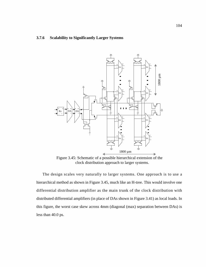
104
3.7.6 Scalability to Significantly Larger Systems
The design scales very naturally to larger systems. One approach is to use a
hierarchical method as shown in Figure 3.45, much like an H-tree. This would involve one
differential distribution amplifier as the main trunk of the clock distribution with
distributed differential amplifiers (in place of DAs shown in Figure 3.41) as local loads. In
this figure, the worst case skew across 4mm (diagonal (max) separation between DAs) is
less than 40.0 ps.
1800
µm
1800 µm
+ +
- DA-
+ +
- DA-
+ +
- DA-
+ +
- DA-
+ +
- DA-
+ +
- DA-
+ +
- DA-
+ +
- DA-
+
-
+Rx
-
+
-
+
- DA
+
-
+
- DA
Figure 3.45: Schematic of a possible hierarchical extension of the clock distribution approach to larger systems.

105
3.7.7 Disadvantages of the Clock Distribution Scheme
The disadvantage of this clock distribution method is that it consumes a lot of area.
The area penalty for clocking is approximately 50% of the layout area of the interface.
This is in large part due to the fact that we operate close to the edge of the capability of 0.8
µm CMOS process technology. A better approach is to redesign the clocked circuitry in
the data channels so that they can operate with low-voltage swings. At the same time, we
design the clock buffers so that they are robust to a large variation in clock loads. An
efficient way of doing this is to use a clock driver whose output impedance is low, so that
the output of the clock driver can be modeled as a voltage source. Inverter clock drivers
and conventional differential amplifiers have a high output-impedance, making the output
clock waveform sensitive to capacitive loading. Local amplification of low-swing clocks
accrues the penalty of high power consumption of the local clock amplifiers. This can be
avoided if the local clocked circuits do not need large swing clocks.
3.7.8 Low Output-Impedance Clock Driver
The low output-impedance clock driver is implemented as a three-stage amplifier as
shown in Figure 3.46. The first stage is a broadband regulated gain cascode [208][209]
amplifier with APLSD load devices consisting of devices M1-M4, M6-M8, M12-M13 and
M16-M19 in Figure 3.46. The second stage is a large-swing differential buffer amplifier
(M9-M11, M20-25) with a level-shift stage (M26-M29). The level-shift driver outputs
(Vo2+ and Vo2-) drive the capacitive load of the clock line as a push-pull driver. Even
though the body effect of the upper NMOS transistor (M26, M28) makes it harder to
drive, the insensitivity of the driver’s voltage swing to variations in output capacitance of
about 0.5 pF for a 2.0 pF rated driver makes it very attractive. The optimal voltage swing
of the output was found to be from 0.8 V to 2.1 V, which is suitable to drive the clocked
transistors in differential flip-flops as in Figure 3.12 and Figure 3.20. The low output-

106
impedance of the level-shift driver makes it very tolerant to large capacitive load variation
compared to a differential-amplifier based clock driver shown in Figure 3.39. In addition,
the low output-impedance greatly reduces the duty-cycle variation due to NMOS and
PMOS transistor process parameter variations compared to an inverter-based or a
differential amplifier-based (Figure 3.39) clock driver.
The clock driver drives the clock distribution line from the center (which gives one-
fourth the skew compared to driving the clock line from either end). The clock lines are
10 µm wide, with 6 µm spacing to minimize the Miller multiplication of the fringing
capacitance between the differential clock signal lines. The simulated amplitude of clock
channel waveforms in an IC with a clock distribution channel 4.3 mm long is plotted in
Figure 3.47. The simulation setup assumes an array of three clock drivers, sized to drive
1.3 V across 6 pF of gate and wire capacitance. The full clock distribution network, from
the input pads (which receive a 400 mV LVDS clock signal) with intermediate amplifiers,
is included in the simulation. The simulation is done using the slow process corner model
Vin+ Vin-
Vo1-
M1 M2
vbias1
Figure 3.46: Schematic of controlled peaking amplifier implemented with regulated cascode amplifier input stage followed by output stage with controlled zero insertion by the control signal srcntrl.
M5
Vo1+
M3 M4 +-M6 M7
vbias1 M8
M9 M10
vbias1 M11
Vo1+ Vo1-
Vo2-Vo2+
M12 M13
M16
M17
M18
M19
APLSD load Cascode RegulationAmplifier
Output Stage with Controllable Peaking
M20 M21
M22
M23
M24
M25
M27 M29
M28M26

107
decks in the 0.5 µm CMOS model library at a junction temperature of 85 °C. The flip-
flops, which are driven by the clock waveform whose amplitude is plotted in Figure 3.47,
need an amplitude of approximately 1.1 V in order to operate as designed. It is evident that
there is almost a 50% capacitive load margin built into the clock driver because of the
choice of the output driver.
Delay elements and multiplexers are an important part of the clock path on a high-
speed data link. Delay elements are used to control the phase spacing of the clock and data
on the IC. Multiplexers are used to select from among different clocks. Delay elements
tend to be implemented as buffers with a slow-path and a fast-path formed by turning on a
second driver in parallel with the slow-path. The difference in delay between the two
configurations forms the basis of a delay element. A cascade of these delay elements, each
of which is controlled by a bit in a control pattern, forms a delay chain. The control pattern
bits determine which elements of the delay chain are in the fast-mode and which are in the
slow-mode. This enforces a granularity of as much as 90 ps in the delay that can be
Figure 3.47: Simulated amplitude of clock channel waveforms of an array of three clock drivers (Figure 3.46) driving the capacitive loads (gate + wire) indicated on the x axis.

108
achieved. This technique works well at the speeds for conventional digital circuitry (for
example, 250 MHz in 0.5 µm CMOS process technology). It does not work well at much
higher speeds (for example, 1.25 GHz in 0.5 µm CMOS process technology) due to the
capacitive loading of the additional signal path. We used the delay elements developed for
the Voltage Controlled Oscillator (VCO), which is discussed in Chapter 4, to implement
an analog delay line with infinite resolution. We do not implement a Delay-Locked Loop
(DLL) to automatically set the delay in the delay chain required to achieve the desired
clock-to-data phase spacing.
Multiplexers are very important elements in the clock distribution path because they
allow us to select between different clocks, for example, between an on-chip clock from a
PLL and an external clock. The selected input clock waveforms should be sent to the
output with minimum time and amplitude jitter. The input clock which is not selected
should not interact with the output of the multiplexer, resulting in increased time and
amplitude jitter of the output. The multiplexer should also not allow the input clocks to
interact with each other. The schematic of a differential 2:1 multiplexer is shown in Figure
3.26. This circuit has input data-dependent distortion at the outputs due to coupling of
parasitic device channel capacitance and parasitic capacitance at the source of the upper
differential pair of the multiplexer that is not selected. For example, if signal S- is logic 0
in Figure 3.26, transistor M2 is off and transistor M3 is on. The output is then controlled
by the input signals D2+ and D2- through transistors M5 and M10. During this time, D1+
(D1-) may be on (off) or off (on). This causes variations in the trout- (tfout-), the rise- (fall-)
time of OUT-, and tfout+ (trout+), the fall- (rise-) time of OUT+. When D1+ is on and D1- is
off, transistor M10 sees the channel capacitance of transistor M9 and the parasitic
capacitance at the source of transistors M4 and M9, which increases the rise- or fall-time
of OUT-, while M5 does not see this extra capacitance. When D1+ is off and D1- is on,
transistor M5 sees the channel capacitance and the parasitic capacitance associated with

109
the source of transistors M4 and M9. This increases either the rise- or fall-time of OUT+.
This input data-dependent output loading becomes more significant at higher operating
frequencies because the rise- or fall-time of a voltage signal across a capacitor is
proportional to the amount of current available to charge the capacitor. This data-
dependent capacitive loading of the output is a significant source of time and amplitude
jitter at the multiplexer output, especially when the inputs are at different frequencies or at
a phase difference other than 180°. When the inputs are at the same frequency, but at a
phase difference of 180°, it is obvious that this issue does not arise.
One solution is shown in Figure 3.48 for a multiplexer that selects between two clocks
labeled D1+/- and D2+/-. The clock input(s) that are not selected are disabled. We
implement this by passing each clock input through a 2:1 multiplexer, which is connected
so that when the clock is not passed through it, both the positive and negative differential
output voltage of that multiplexer are at a dc-value close to ground potential. This dc-
potential is the potential that appears at the input of the clock multiplexer that actually
drives the output clock path. Hence, there is no input data-dependent time and amplitude
Figure 3.48: Schematic and symbol of low-jitter 2:1 clock select multiplexer.
D1
D2
2:1 multiplexer
sel
selb
D1+,D1-
s-s+
D1
D2
2:1 multiplexer
sel
selb
OUT+,OUT-
D1+,D1-
D2+,D2-
s-s+D1
D2
2:1 multiplexer
sel
selb
D2+,D2-
s-s+
selb
sel
sel = 1, selb = 0 selects input D1sel = 0, selb = 1 selects input D2

110
jitter at the clock multiplexer output. The disadvantage of this method is the increased
power consumption due to the additional multiplexers.
3.8 Electrical Receiver Circuit
The original electrical signaling on the POLO electrical interface is a PECL interface
[54], a positive 5.0 V power supply version of the ECL signaling standard [53]. This
signaling then migrated to the LVDS standard [20] because receiver performance
(bandwidth, input capacitance and power consumption) in CMOS process technology is
best for differential signals with a common-mode of half the power supply voltage.
We design our receivers with passive resistive-input termination of 50 Ω resistors for
parallel-load termination [53] to a termination voltage called VTT as shown in Figure 3.49.
Passive resistors are used instead of active termination circuits because passive resistors
are inherently broadband devices. We avoid the use of feedback control circuitry and
control lines, and achieve operation over a wide range of frequencies by choosing passive
Vin+ Vin-
Vo1-
M1 M2
vbias1
Figure 3.49: Schematic of controlled peaking amplifier implemented with regulated cascode amplifier input stage followed by output stage with controlled peaking implemented by the signal called srcntrl.
M5
Vo1+
M3 M4 +-M6 M7
vbias1 M8
M9 M10
vbias1 M11
Vo1+ Vo1-
Vo2-Vo2+
srcntrl srcntrlM12 M13M14 M15
M16
M17
M18
M19
M20 M21M22 M23
APLSD loadwith zeroinsertion peaking Cascode Regulation
Amplifier
Output Stage with Controllable Peaking
R1
VTT VTT
R1

111
resistors. The sheet resistance, ρ, of salicided polysilicon in HP-CMOS14 0.5 µm CMOS
process technology is approximately 2 Ω/square from run to run, according to MOSIS run
measurements, and was therefore used to implement the input termination resistors. The
resistor has a width significantly greater than the minimum feature size, and close to the
four-terminal Van der Paw test structure of a square of 24 µm x 24 µm salicided
polysilicon that MOSIS uses for salicided polysilicon sheet resistance measurements. The
receiver amplifier is designed with the minimum number of cascaded amplifier stages.
This helps to minimize the bandwidth requirement of each amplifier stage, avoid a long
chain of dc-coupled amplifiers, which in turn reduces the dc-drift problems associated
with dc-coupled amplifier chains. In addition, it reduces the need for complicated bias
control mechanisms. We design for a differential input sensitivity of 50 mV. This is
balanced by the consideration of minimizing the capacitance looking into the circuit from
the input termination resistance, which sets the input time-constant of the electrical
receiver. The receiver amplifier consists of a cascade of two stages, the first of which is
implemented as a regulated gain cascode [208][209] amplifier with APLSD load devices
consisting of devices M1-M4, M6-M8, M12-M13 and M16-M19 in the schematic in
Figure 3.49. The second stage is a differential amplifier stage with controlled peaking. We
adapt the method of increasing the bandwidth of current-mirrors by resistive
compensation proposed by Toumazou et al. [196], to implement controlled peaking in the
second-stage amplifier. We insert a zero into the amplifier input-output transfer function
by the use of transistors M22 and M23, which function as voltage controlled resistors. The
zero is inserted at -1/RCgs, where R is the drain-to-source resistance of M22 or M23, and
Cgs is the gate-to-source capacitance of M20 or M21. Changing the gate voltage (signal
“srcntrl”) of transistors M22 and M23 in Figure 3.49, modifies the resistance of these
devices, which alters the location of the zero, controlling the amount of peaking and the
frequency at which the gain-peaking occurs.

112
3.9 PECL/ECL Transmit (Tx) Circuit
The 5.0 V PECL [54] electrical signaling standard requires an 800 mV swing with a
common-mode voltage of 3.7 V when the signal is terminated to a termination voltage
VTT of 3.0 V through a 50 Ω termination resistor. The termination can be a parallel
termination of a 50 Ω resistor to VTT at the load end, or a series termination consisting of
an 81 Ω resistor from power to load and a 131 Ω resistor from load to ground, as discussed
earlier (Section 3.10 on page 114). The voltage signaling requirements translate to an
output current requirement of a dc-current of 14 mA with an ac-swing of +/- 7mA
superimposed on the output dc-bias current. CMOS circuit realizations of ECL and PECL
transmitters/drivers have been the subject of much work in the literature. A brief summary
of CMOS PECL/ECL drivers is given in Table 3.2.
Data Rate
(Gb/s)
Process Technol
ogyTechnique Area (µm x
µm)Power (mW) Ref
0.1 0.9 µm CMOS
NMOS source follower driving PMOS common source driving inverter (Rx)
single-ended class AB output stage with Voh,Vol reference
90 x 140 Rx635x780 Tx
16.9 (Rx)108 (Tx)
[68]
0.1 0.7 µm CMOS
Single-ended PMOS common source output with differential to common-mode feedback
loop to supply correct output drive (Tx)
200 x 125 56 [73]
0.15 1.2 µm CMOS
NMOS source follower driving Diff. amp. driving inverter chain (Rx)
Single-ended common source cascade with feedback and compensation (Tx)
175 (Rx+Tx)
[69]
0.7 0.5 µm CMOS
Differential Common Gate receiver with class AB output stage (Rx)
Single-ended NMOS source follower driving PMOS Common source with current source
load (Tx)
[70]
0.0235
2 µm CMOS
Single-ended Differential input stage with current mirror load (Rx) driving inverter
single-ended switched current source output stage (Tx)
190x240 (Rx)
200 x 500(Tx)
2.2 (Rx)15 (Tx)
[71]
Table 3.2 PECL/ECL IO circuits.

113
The PECL/ECL voltage signaling levels can be viewed as a current signaling level
requirement which gets converted to a voltage by the termination resistor at the load end.
Parallel termination to VTT at the load end means that a good match of the termination
resistor to the line impedance will prevent reflections from coming back to the source
(assuming that the line impedance is constant and does not cause any reflections). This
means that the PECL/ECL output stage can be viewed as a current source.
Since the successful interface to a Bipolar ECL/PECL style receiver (for example, the
POLO module electrical receiver circuit) with parallel termination to VTT = 3.0 V through
a 50 Ω resistor, requires the sourcing of current, the final output stage is chosen to be an
3 µm CMOS
Inverter with transistors in cutoff or saturation (Tx)
[72]
1 0.8 µm CMOS
Differential NMOS source follower driving NMOS differential pair driving inverter (Rx)Differential NMOS stage with PMOS current
mirror and PMOS open drain output stage (Tx)
410 x 337 (Rx)
235.6 x 250 (Tx)
220 (Rx)561 (Tx)
[9]
Data Rate
(Gb/s)
Process Technol
ogyTechnique Area (µm x
µm)Power (mW) Ref
Table 3.2 (Continued) :PECL/ECL IO circuits.
CMOS2 PECLTx
O+
O-D-
D+
D+,D- O+,O-
Figure 3.50: Schematic and symbol of differential CMOS2PECL Transmit (Tx) circuitry.
M4
M5
M6 M7
M3
M8
M9
bias

114
open-drain PMOS transistor [132]. This PMOS transistor is designed to supply the dc-bias
current of 14 mA and the ac swing of +/- 7mA for each output of the differential pair. The
PMOS output transistors (M8 and M9 in Figure 3.50) are in turn driven by an NMOS
differential pair with diode-connected loads (M1-M7 in Figure 3.50), to ensure minimum
variation in bias points. The NMOS differential input pair is over-driven by inverters to
overcome the large parasitic gate-to-source capacitance of the PMOS output stage. The
disadvantage of this circuit topology is the fact that the output transistor and the pre-driver
load transistors are not in the saturation regime of operation throughout the duration of the
output voltage swing. This results in a long tail on the fall-time as can be seen from the
eye-diagram in Figure 3.12. This is forced by the biasing requirements of PECL/ECL
signaling standard. A symmetric, interleaved layout strategy was used to minimize the
impact of process-dependent spatial variations on the transistor sizes. Separation of power
and ground lines to minimize power-supply coupling is also used.
3.10 LVDS Transmit (Tx) Circuit
The bandwidth limitations imposed by the PECL/ECL signaling standards on the
CMOS Rx and Tx circuitry are removed by migrating to the LVDS standard [20], which
specifies a common-mode voltage of 1.2 V (for a supply voltage of 2.4 V). Transmitters
and Receivers are easiest to design when the output common-mode voltage is such that the
circuit transistors can remain in saturation for the duration of the signal swing. An output
common-mode of half the power supply voltage is usually a good choice.
Each output line is parallel load terminated to a termination voltage VTT_Tx, through a
50 Ω resistor, as shown in Figure 3.51. The 50 Ω termination resistor establishes the bias
of the output transistor of the CMOS driver (Figure 3.53), when the optional source
termination resistor is not connected. Figure 3.51 shows the schematic of a CMOS IC,
with a high-speed interface of parallel load terminated LVDS Tx circuits driving data

115
from the CMOS Tx IC to IC2, which may be a CMOS, Si/SiGe BJT, GaAs MESFET or
other advanced process technology IC. VTT_Tx is the termination voltage at the receiver
end, which sinks current and sets the bias of the CMOS Tx circuits. Parallel load
termination in LVDS and PECL requires that the termination voltage sink current (see
Appendix A for a current-sinking termination voltage specification and schematic).
An alternate solution which removes the need for a current-sinking termination power
supply is to replace the 50 Ω resistor with a series connection of 81 Ω and 130 Ω resistors
between power and ground, whose thevenin-equivalent resistance is 50 Ω. The
disadvantage of this mechanism is the increased standby power dissipation due to the 211
Ω resistor connected between power and ground (which results in 128.8 mW of standby
power dissipation for every differential output pair compared to the 16.4 mW of standby
power dissipation for the LVDS parallel load terminated case, assuming a power supply of
3.6 V and a termination voltage of 1.55 V in the LVDS case). Considering that eight
output channels would result in the dissipation of 1 W, the standby load-termination
power-dissipation associated with the alternate method becomes a very significant
percentage of the power dissipation of the entire IC, in the case of parallel electrical data
links.
+- VTT_Tx
50 Ω Transmission Line
50 Ω Receiver
IC 2
Figure 3.51: Schematic of the interface connection of 2.5 Gb/s LVDS CMOS Tx cir-cuit. IC2 can be Si-Bipolar or future CMOS IC.
CMOS Tx
direction of data flow

116
Figure 3.52 shows the schematic of the high speed interface for data flow from a Si
BJT or other advanced process technology IC to the CMOS IC. VTT_Rx is the termination
voltage at the receiver end, which may sink or source current. The transmit circuit is
designed to accommodate the following applications:
• Drive a parallel load terminated 3.3 V PECL receiver through a 50 Ω transmission
line
• Drive a common N-substrate6 VCSEL in a VCSEL array
• Drive a floating 100 Ω resistor at the receiver, following the LVDS standard when
source termination is included in the transmit circuit
The design considerations for the transmit circuit from an IC design point of view are
the highest bandwidth, for the least amount of power consumption, and the least amount
of power-supply and substrate noise generated on the IC. The transmit circuit schematic
shown in Figure 3.53 is a modified version of the PECL transmit circuit (Figure 3.50)
discussed earlier in this section. Its circuit bias-levels have been modified to take
6. Refers to an array of VCSELS grown on an N-type substrate such that thepositive terminal of each VCSEL diode is driven by a distinct transmit circuit.
+- VTT_Rx
50 Ω Transmission Line
50 Ω Receiver
IC 2
Figure 3.52: Schematic of the interface connection of the 2.5 Gb/s CMOS Rx circuit. IC2 can be Bipolar or future CMOS IC.
CMOS Rx
Transmitter
direction of data flow

117
advantage of the altered signaling levels. The pre-driver differential amplifier stage
outputs (Vo1+ and Vo1-) in the transmit circuit are RC-limited and exhibit a long fall-time
due to the limitation imposed on the discharge current path, by the tail-current source M5
in the differential input stage. The output transistor is now biased so that it is in the cut-off
region for most of the duration of the fall-time of the pre-driver stage, so that we get clean
open eye-diagrams as in Figure 5.21 (a).
.
The APLSD load in the pre-driver, consisting of transistors M12-M13 and M16-M19
in Figure 3.53, enable increasing voltage swings at the inputs of the output transistors M3-
M4. This allows us to reduce the size of these devices, as the current that is required to
flow in the link can be obtained with smaller device sizes. This allows us to reduce the
power consumption and increase the bandwidth of the transmit circuit. Transmitter
peaking may be obtained by the insertion of a zero in the transfer function of the pre-
driver, by inserting resistors implemented by transistors M14 and M15 in the APLSD load
(as discussed in Section 3.8 on page 110).
Figure 3.53: Schematic of differential LVDS Transmit (Tx) circuitry with optional source-termination resistor R1.
Vin+ Vin-
Vo1-
M1 M2
vbias1 M5
Vo1+
M12 M13M14 M15
M16
M17
M18
M19
APLSD loadwith zeroinsertion peaking
O+O-
R1 R1
VTT VTT
M3 M4

118
The output driver may have optional source-termination resistors to VTT, which is a
voltage source that sinks current and has a value between 3.0 V and 0.0 V, depending on
link biasing and bit rate considerations. The LVDS transmit circuit in Figure 3.53
dissipates 27.8 mW, to achieve 400 mV output swing in a parallel load terminated link at
data rates up to 3.3 Gb/s. The measured performance of the different LVDS and PECL
transmit circuits in 0.5 µm CMOS is detailed in Table 3.3.
3.11 0.5 µm CMOS LVDS Rx-Tx Measurements
The common-mode voltage requirements of the CMOS Rx and Tx circuits for the
high-speed interface are measured on the Rx-Tx circuits fabricated in the HP-CMOS14TB
process (IC T6). The measurements are performed in setup S-1 (Figure 3.54). S-1
measurements are done with termination voltages VTT_Rx and VTT_Tx being equal (S-1a),
and with termination voltage VTT_Rx fixed and VTT_Tx varying (S-1b). S-1b is used to
Driver Type Tech. (µm)
Supply Voltage
(V)
VTT (V)
Power Dissipa
tion (mW)
Data rate
(Gb/s)
Area (µm
x µm)
Output Amplitude (mV)
LVDS (no source term). 0.5 3.6 1.55 27.8 3.3 196 x235
400
LVDS (with 50 Ω sourceterm.), floating 100 ohmload
0.5 3.6 1.55 27.8 3.3 196 x235
200
PECL 0.5 3.6 2.16 155.8 2.5 177 x188
800
PECL 0.5 5.0 3.00 910 2.5 177 x188
800
PECL 0.8 5.0 3.00 561 2.0 235.6x 250
800
Table 3.3 Comparison of LVDS and PECL Transmit circuits in parallel load termination
configuration.

119
determine the variation of output characteristics with output common-mode voltage. Note
that since the test setup is ac-coupled, VTT_Rx and VTT_Tx in S-1 correspond to the
common-mode voltage of the input and output waveforms. VTT_Tx can be between 0 V and
2.0 V when a bias-tee is used to observe the output on the oscilloscope.
Figure 3.55 shows the small-signal response of a circuit whose schematic is shown in
the inset on the right, which has been implemented in 0.5 µm CMOS. A single-ended
insertion-gain measurement gives a measured -3 dB bandwidth of 1.7 GHz. The small-
signal insertion-gain measurement is done by injecting +3.0 dBm of power through a bias-
tee from an Agilent 85645A tracking source into the positive input of the Rx circuit, and
measuring the response of the output through a bias-tee, using an Agilent 8564E spectrum
analyzer. Bias-tees are used so that the inputs and outputs of the Rx and Tx circuits are
properly biased. The inset on the left in Figure 3.55 shows the output eye-diagram of the
Rx-Tx circuit for a 3.3 Gb/s 231 - 1 NRZ PRBS input data stream with an amplitude of
200 mV. The vertical scale is 200 mV/div and the horizontal scale is 50 ps/div. Table 3.4
details the measured output data characteristics for test setup S-1a. The input amplitude is
determined by programming the BERT. VTT_Tx and VTT_Rx are the same and are
controlled by setting the value of the voltage sink. The eye-width and eye-height are
+-VTT_Rx
50 Ω Transmission Line
50 Ω Rx1 --> Tx1
Figure 3.54: Schematic of setup one (S-1) interface connection.
BERT
Scope
BERT
+- VTT_Tx CMOS IC

120
measured by the BERT at BER < 10-3. Vamplitude and Vp-p are measured by the
oscilloscope.
.
The nominal common-mode voltage is 1.75 V. The objective of the measurement was
to determine the maximum input common-mode voltage for error-free CMOS Rx
performance. The performance of the CMOS Tx is shown by the data on eye-height, eye-
width, output amplitude (Vamplitude), and peak-to-peak output voltage (Vp-p) in Table 3.4
for different VTT_Tx at different data rates. Again, it is of interest here to determine the
Schematic of circuit whose small-signal response is shown. VTT = 1.55 V.
Rx Tx Buf
VTT50Ω
50Ω
3.3 Gb/s
Figure 3.55: Insertion-gain measurement of CMOS Rx-Tx circuit on IC T8 with inset of 3.3 Gb/s eye-diagram corresponding to 231 - 1 NRZ PRBS from the BERT and the schematic of the test circuit on IC T8. See text for details.

121
Data Rate
(Gb/s)
Input Amplitude (mV)
VTT_Rx = VTT_Tx
= (V)
Eye-Width (ps)
Eye-Height (mV)
VAmplitude (mV)
Vp-p (mV)
Comment
1.5 50 1.75 600 266 392 476
2.25 581 183 284 352
2.35 567 132 236 288 srcntrl=3.3 V
2.0 50 1.75 426 221 396 476
2.15 421 165 344 412
2.25 409 124 292 354
2.35 384 78 240 284 srcntrl=3.3 V
2.5 50 1.75 325 159 404 476
2.15 296 96 324 388
200 1.75 350 221 432 504
2.25 309 171 372 420
2.45 272 115 304 372 srcntrl=3.6 V
2.8 200 1.75 301 196 428 504
2.25 261 141 352 416
2.35 244 112 336 396 BER < 10-12
2.45 223 75 304 364 BER < 5 x 10⁻⁹
3.3 80 1.75 221 91 404 492
2.10 180 53 372 428 BER<2x10⁻¹⁰
200 1.75 241 149 424 504
2.25 189 86 352 412 srcntrl=3.6 V
Table 3.4 Summary of measurements of setup S-1 when VTT_Rx=VTT_Tx = common-
mode voltage of input and output signals.

122
maximum value of VTT_Tx for acceptable performance. All measurements in Table 3.4
correspond to a BER < 10-12 unless otherwise noted.
3.12 Summary
This chapter described the design and implementation of the critical components of a
2.5 Gb/s/channel parallel data link in 0.5 µm CMOS: high-speed differential flip-flop and
logic gates, electrical LVDS receiver and transmit circuits, and robust low-skew clock
distribution circuitry. The high-speed differential flip-flop whose design has been guided
by the choice of our low-swing differential voltage-mode clock buffer, which has a large
tolerance to capacitive load variations, and the choice of our low-parasitic capacitance
APLSD load device. The flip-flop circuit technique developed in this chapter is extended
to form a high-speed differential logic family that can be merged successfully into the flip-
flops that have been developed. High-speed NAND/AND gates so developed were used
successfully with the above components, to implement 4/5, 4/6 and 4/5/6 prescalers, each
of which was measured to operate up to 2.1 GHz. We have demonstrated a technique to
distribute high-speed clocks in large VLSI systems with sub-50 ps skew. The
attractiveness of this approach is the considerable reduction in power-supply noise and
substrate-coupled noise introduced into the system by a high-speed clock due to the low-
swing differential nature of the clock. We have also demonstrated low-power electrical
LVDS transmit and receive circuits, each consuming approximately 30 mW, which
achieved 3.3 Gb/s of error-free data transmission corresponding to 231 - 1 NRZ PRBS
input data patterns with 70 mV of differential input amplitude.
The components described here are used in the implementation of a wide-range low-
jitter x2/x4 Phase-Locked Loop based Frequency Synthesizer (PLLFS) (Chapter 4), a 12
wide 2.5 Gb/s/channel 2:1/1:2 mux/demux array IC (Chapter 5) and a 12-wide opto-
electronic receiver array (Chapter 6). In Chapter 6, we shall see that we can use the same
123
electrical transmit driver described in this chapter to directly drive VCSEL diodes,
achieving 2.5 Gb/s error-free data transmission at one-fourth the power consumption of
electrical LVDS transmit circuits.

124
Chapter 4
PLL based Frequency Synthesizer Design
A 4:1 or 2:1 multiplexer/demultiplexer and a high-performance Phase-Locked Loop
based Frequency Synthesizer (PLLFS) is needed to interface fast-narrow synchronous
parallel fiber-optic interconnects to slow-wide parallel electrical interconnects such as
HIPPI-6400. The required PLLFS is characterized by very low-jitter to minimize system
insertion penalty, selectable times-2 (x2) or times-4 (x4) frequency multiplication, a wide
frequency range to accommodate different system clock speeds and graceful system
degradation, and high maximum-frequency of operation for data rates in excess of 2.5 Gb/
s per signal line.
In this chapter we discuss the components of the PLLFS required to achieve sub-50 ps
peak-to-peak jitter to enable data transmission at 2.5 Gb/s (400 ps bit time) over VCSEL-
based parallel optical data links. The jitter requirement is stringent because of the high
turn-on delay jitter of semiconductor-based lasers (for example, VCSELs and edge-
emitting lasers), which implies that the jitter contribution from the electronics circuitry has
to be as low as possible. We motivate the choice of a ring oscillator instead of a low phase-
noise LC oscillator, and the choice of the delay cell used in the oscillator. The circuit

125
technique used to realize an analog adjustable Voltage Controlled Oscillator (VCO) gain,
which has been key to achieve the low, measured jitter on our fabricated PLLICs is
discussed. Noise sources and injection mechanisms are considered, and design techniques
are incorporated to reduce their impact. The Phase Frequency Detector (PFD) is a key
component of the PLLFS. We discuss the circuit techniques used to achieve the stringent
requirements of the PFD due to the low multiplication factor of the x2/x4 PLLFS. This
means that the PFD has to operate at a much higher frequency compared to conventional
x20 or x30 PLLFSs. The loop-filter choice is critical to the proper functioning of the
PLLFS. This issue is discussed in the loop-filter section (Section 4.4 on page 190), where
the measurements from the VCO testdie are used to arrive at the appropriate selectable
loop-filters for the final PLLFS IC. The last section covers the measured results of the
PLLFS IC, which is 3.3 mm x 1.65 mm and consumes 1.2 Watts from a 3.6 V supply.
A wide frequency-range and high maximum frequency of operation is achieved using
a ring oscillator with a minimum number of delay cells. The design is based on an ECL-
style latch with a cross-coupled stage and level-shifted diode-connected PMOS
transistors. The current in the delay cell is adjusted using differential control of
independent current mirrors that control the differential and cross-coupled parts of the
cell. The output jitter of the delay cell increases when more current flows in the cross-
coupled pair (when the delay of the cell is increased) due to the increased uncertainty in
the switching threshold of the cross-coupled pair. This is acceptable because it is easier to
absorb jitter at lower data rates.

126
The frequency range of a VCO is usually inversely proportional to its phase-noise. We
avoid this by adopting an architecture in which the slope and offset of the VCO transfer
characteristic are adjustable. The VCO control stage is a linear rail-to-rail transresistance
circuit with independently adjustable gain and offset controls. This gives direct control of
the tuning and frequency range of the VCO. In a system, this feature may be used to
interface to a digital control circuit that puts the VCO in a high-gain setting to acquire the
signal, and then automatically change the gain to reduce the jitter of the locked signal
without losing lock. Integrated into a single circuit, this device would form the core of an
intelligent PLLFS.
4.1 Phase Locked Loops:
Phase Locked Loops (PLLs) have been the subject of extensive research ever since
their introduction. An excellent introduction to the basics can be obtained from
[133],[134] and [135]. The system design requirement of the PONIMUX IC, which forms
the vehicle for the system integration experiment of parallel optics and CMOS circuitry,
requires a high-frequency wide-range frequency synthesizer. Figure 4.1 shows the block
diagram of a PLLFS. A PLLFS has four basic components: the oscillator which is the
actual clock source for the PLLFS output, a feedback divider with division ratio N, a Low-
Figure 4.1: Block diagram of a generic PLLFS.
VCOLPFPFD
Divider
Referenceclock x(t)
Output frequency y(t)
1/N

127
Pass Filter (LPF), and a PFD which generates an error signal depending on the phase and
frequency difference between the reference-clock input and the feedback-clock signal.
The LPF filters the output of the PFD, so that a dc-control signal to the input of the
oscillator is generated. Oscillators may be controlled by a voltage (VCO) or a current
(CCO). The division ratio N determines the factor by which the output frequency is a
multiple of the reference clock frequency. If N=1, the PLLFS reduces to a PLL whose
function is to phase-lock the oscillator output to the reference clock signal. This maybe
used to reduce jitter, skew, perform clock-recovery etc. When N > 1, the oscillator
produces N output periods before the PFD can correct it, as the inputs to the PFD arrive
only every N oscillator cycles. In a PLLFS, the noise in the reference-clock source gets
multiplied by N when it gets transferred to the output of the PLLFS.
If the VCO output frequency and the reference-clock frequencies are different, the
PFD produces an error signal whose dc- or mean-value is the control signal of the
oscillator output frequency. The oscillator integrates frequency to give phase. In the loop,
if the PFD signal is such that the reference clock is ahead of the VCO feedback signal, the
control voltage to the VCO is increased. The VCO frequency increases so that PLLFS
accumulates phase at the output by changing frequency to drive the phase difference
between the input reference-clock signal and the oscillator feedback signal to zero.
A PLL or a PLLFS is a control system where the variable of interest is phase -- not
frequency, voltage or current. The control variable changes around the loop from phase to
voltage across the PFD and voltage to phase through the oscillator. A linearized model of
the PLLFS in Figure 4.1 is shown in Figure 4.2. In the context of the PLLFS control loop,

128
the oscillator converts voltage to frequency, which is the time derivative of phase. In other
words, phase is the integral of frequency. Therefore, the input-output transfer function of
an oscillator with gain Ko rad/s/V, in the context of a PLLFS control loop, is given by
(4.1)
The PFD behaves as a Phase Detector (PD) in the linearized PLLFS model at lock. In
other words, the Frequency Detector (FD) is active only when the system is acquiring the
signal. The phase detector gives an output voltage- or current-signal, which is linearly
proportional to the phase difference between the input and output clock signals. The
output of a PD is often a train of pulses, whose dc-mean value is the desired control
voltage to the oscillator. The transfer function of the phase detector is then
(4.2)
where Vcont is the dc-mean value of the PFD output, Kd is the PFD transfer function
whose units are V/rad, and ∆φ is the phase difference in phase between the input reference
signal and the oscillator feedback signal.
φout s( )Vcont s( )------------------
Ko
s------=
F(s)= KO/sφin
φout/N
φe=φin-φout
Kd
1/N
Figure 4.2: Linearized model of the PLLFS at lock.
+
-
φout
KhL(s)
Vcont Kd∆φ=

129
The LPF function, F(s), can be represented as KhL(s), where Kh is the constant
attenuation1 factor in the LPF transfer function. Ko has units of rad/s/V, Kd has units of V/
rad and Kh is dimensionless. The open-loop transfer function of the PLLFS is Ho(s) =
KdF(s)Ko/Ns = KdKh(Ko/N) L(s)/s = K L(s)/s. K is the open-loop gain by convention,
even though it is missing the 1/s factor representing the integration of frequency to give
phase in the oscillator. K has units of 1/second. A single-pole LPF is given by L(s) = 1/
(1+s/ωL) = 1/(1+sRC). The closed-loop transfer function of the PLLFS is given by H(s) =
φout(s)/φin(s) = Ho(s)/1+Ho(s), where Ho(s) = KL(s)/s.
(4.3)
4.2 VCO Design
The system design requirements of a broadband parallel data link require a broadband
PLLFS. A broadband PLLFS naturally requires a wide-range VCO. Increasing the
1. In an active filter, this constant factor can represent gain.
H s( )φout s( )φin s( )----------------- KL s( )
s KL s( )+-----------------------= =
Figure 4.3: Wide-range VCO design choices.
Vcntrl
fmin
fmax
Large Ko
ReducedRangeVCO
1/MN
1/M
VCO1 mux
Reduced Range
VCOn
m
u
xprogdiv.VCO
(a) (c)
(b) (d)

130
frequency range of an oscillator, be it a VCO or a CCO, increases the phase-noise of the
oscillator. The simplest explanation is that as the frequency range of the VCO increases,
the change in the oscillator output frequency due to noise (oscillator thermal noise, power-
supply noise, substrate noise, and noise induced on the control port of the oscillator)
increases as well. Since the PLLFS integrates frequency to give phase, this results in
increasing phase-noise or time jitter at the PLLFS output. The design approaches (Figure
4.3) to a wide range PLLFS include:
• Single VCO (Figure 4.3 (a)), which has the range to accommodate the desired
frequencies. This usually means that the gain Ko of the VCO is very large, with
corresponding requirements on the phase-noise characteristics on the PLLFS
divider, PFD and the loop-filter. The power-supply ripple becomes a significant
consideration, which could easily be the dominant factor degrading system
performance depending on the VCO range and the desired VCO jitter or phase-
noise requirement [170].
• Virtual VCO (Figure 4.3 (b)), which is composed of a VCO and divide-by-1, -2, -4
and -8 circuits, which can generate a VCO with a virtual range of, say, 0.125-to-2
GHz from an intrinsic range of 1 to 2 GHz. The cost of this approach is that a clock-
select mux is required for the divide-by-1 case, because of the fact that in a two-
level implementation of a mux, the native frequency and the divided frequency
interact (Section 5.3.1 on page 230), affecting the rise- and fall-times of the output,
leading to correlated amplitude- and phase-variation of the virtual VCO output. A
further cost is that the divide-by-2, -4 and -8 circuits must be implemented by

131
prescalers to minimize the PLLFS output phase-noise (but the specific phase
relationship is not an important criterion because the PLLFS locks the phase of the
output of the dividers to the reference clock signal). A final cost is the issue of
injection-locking of the PLLFS to the divider output frequency.
• Reduced range VCO with a programmable divider outside the loop of the PLLFS
as shown in Figure 4.3 (c). The loop divides by NM where M is the division ratio
of the programmable divider. The output of the loop is then divided-by-M to
generate the times N signal. Both solutions require the extra power consumption of
the clock-select mux and the programmable divider. Additionally, it is not possible
to arbitrarily decrease the gain (Ko) of the real VCO, and still have access to the
entire range of frequencies. If for example, the range of the native VCO is from 1.5
to 2.0 GHz, then a division by 2 will result in the virtual VCO having a range from
0.75 to 1.0 GHz, missing the range of 1.0 to 1.5 GHz. It is not feasible to do a divide-
by-1.5. A divide-by-2.5 can be implemented at the likely cost of increased jitter for
this operation, compared to division by integer values. This jitter is a result of the
logic operation at high-frequencies to obtain the non-integer division ratio.
• Virtual VCO composed of multiple VCOs as shown in Figure 4.3 (d), is another
possibility. This approach capacitively loads the loop-filter output, necessitating a
buffer. Multiplexers and control bits are required to select the appropriate VCO.
Low-jitter ring-oscillator design indicates that one has to increase the power
consumption for each VCO to reduce the jitter of each VCO output, and this is
likely to increase the power consumption of this implementation to more than that

132
of the synchronous divider case. Solutions that allow VCOs to be turned off
typically result in a reduction of the maximum frequency that the VCO can achieve
due to the parasitic capacitance associated with the multiple VCOs.
Note that if system design considerations allow, one can design a PLL to have two
distinct narrow ranges, say range1 from 50-to-200 MHz and range 2 from 1-to-1.5 GHz.
range1 is used for testing and range2 for operation. This solution can be implemented
either by using two VCOs or by using a programmable divider.
Since none of the above design choices are desirable, we choose to design a VCO
which is an inherently wide-range VCO and can accommodate a control circuit which
adjusts the gain Ko of the VCO. In this chapter, we discuss the design of the PLLFS which
incorporates a VCO of the above description.
An oscillator used in a PLLFS has four important design requirements. They are
• Wide tuning range.
• Timing accuracy and spectral purity, that is, low jitter and phase-noise.
• Power-supply and substrate noise rejection.
• Linear control-voltage to output-frequency VCO transfer characteristic.
A voltage controlled oscillator can be realized in many ways. They are
• VCOs based on an LC tank or similar resonant circuit.
• Multivibrator VCOs or relaxation oscillators.
• Ring oscillators.
VCOs based on resonant circuits have very low phase-noise characteristics. Until
recently, integrated resonant VCOs have been difficult to realize in CMOS in the GHz

133
range [136][137][138]. The phase-noise of reported LC tank VCOs in CMOS is better
than -85 dBc/Hz at 100 KHz offset, but the tuning range is less than 400 MHz. This range
can be increased by having multiple transconductance stages in parallel, which are
switched on and off depending on the desired range of the VCO. However, this limits the
maximum frequency of operation of the VCO due to capacitive loading of the VCO
output. Multivibrator VCOs are known to have excellent linearity but poor jitter
performance. Ring oscillator based VCOs have worse jitter performance and phase-noise
than resonant VCOs, but have better jitter performance than multivibrator VCOs. The
significant advantage of ring oscillator based VCOs is that they have a large tuning-range
and can readily produce equally-spaced clock edges.
Ring oscillators have poor long-term stability and suffer from significant frequency
drift due to a poorly controlled stage-delay. The delay of the stage or delay cell in a ring
oscillator can vary with temperature and process. When ring oscillators are used in a
PLLFS, the loop corrects for long-term instabilities like frequency drift of the oscillator by
tracking the reference signal. This does not hold for instabilities whose frequencies are
higher than the PLL bandwidth. In other words, the high-frequency jitter of the ring
oscillator based VCO is transferred directly to the PLLFS output.
4.2.1 Ring Oscillator Design
Ring oscillators are composed of electronic delay cells which are connected in a
closed-loop or ring, such that there is a net inversion of signal polarity around the signal-
path. The gain along the signal-path in the closed-loop must satisfy Birkhausen’s criterion
for oscillation. The electronic delay cell must be capable of having its delay adjusted by an

134
external control signal which is in the form of a current or voltage. This control voltage or
current is the control port exploited by the loop in a PLLFS. Typical realizations of an
oscillator use singled-ended gain stages. These gain stages are usually inverters in CMOS.
They are made controllable by stacking a PMOS and an NMOS transistor in series with
the P and N transistor respectively to achieve a controllable delay cell. Low-jitter
oscillators (which are not thermal-noise limited) are realized using differential delay cells
with a differential control path.
Figure 4.4 (a)-(d) show some widely used ring oscillator configurations which are
independent of technology. The control ports are not shown. Each delay element in a ring
oscillator is understood to be a variable delay element. Figure 4.4 (a) shows the topology
of a single-ended oscillator with single-ended delay cells. It is required that the ring be
composed of an odd number of stages so that the signal polarity is inverted around the
ring. The period of the oscillation is equal to 1/(2*number of inversions *td). The single-
ended delay cells can be replaced with differential delay cells to get the oscillator in
Odd number of inversions
Odd number of stages
Even number of stages
Figure 4.4: Single-ended and differential ring oscillator realization.
(a)
(b)
(c)
(d) delay interpolation technique

135
Figure 4.4 (b). The advantage of a differential oscillator is that it can oscillate with an even
number of delay cells, because a wire inversion provides the signal inversion around the
loop as shown in Figure 4.4 (c). Another method of exploiting differential delay cells in
ring architectures is shown in Figure 4.4 (d), which is called delay interpolation. The
shaded block represents a delay interpolation block which smoothly interpolates between
the slow (delayed-by-2 delay cells) and fast (delayed-by-1 delay cell) paths according to
the control signal that it receives. The smallest delay of the composite delay element
would be that of one delay cell while the largest delay would be the delay of two delay
cells. Many variations of this method can designed. Ring oscillators can also be
constructed by using multiple rings whose outputs are mixed [143].
The delay cells shown in Figure 4.4 can be realized in many ways. The simplest
technique is to use a gain-cell cascaded with an RC load, whose time constant is adjusted
by changing the resistance, R, or capacitance, C, by means of an external control signal to
change the frequency of oscillation. An alternate method is to use delay interpolation as
shown in Figure 4.4 (d). The RC load can be the load of the gain cell which is used to
implement the delay cell. Typically, the resistance, R, is the load of the gain cell and the
capacitance, C, is an adjustable capacitive load connected to the output of the gain cell.
Figure 4.5 shows the schematic of a general differential gain cell with possible delay-
adjustment knobs (shaded arrows). The load of the differential stage is shown as a series
combination of resistance (R) and inductance (L) elements. The L-elements may be used
in high-performance microwave oscillators to peak the parasitic capacitance at the output
of the delay cell in a broadband oscillator or to realize a narrow-band oscillator. They are

136
shown here for completeness. Resistive tuning is achieved by adjusting the value of the
load resistances by a control voltage, or by adjusting the value of the tail-current sink ISS,
or a combination of both. The variation of the load resistances is achieved by
implementing them with PMOS transistors biased in the triode region, effectively using
them as voltage-controlled resistors.
The variation of the tail-current sink can be effected either by a current-mode signal or
by a voltage, controlling the gate of a transistor which effectively performs the function of
the tail-current sink. As the time constant of the output decreases by decreasing the load
resistances, the gain of the circuit decreases as well, reducing the amplitude of the
oscillating signal [135]. This makes the oscillator signals more susceptible to noise at high
frequencies, manifesting in increased timing jitter. Moreover, the higher end of the
frequency range is compromised because the circuit fails to oscillate when the gain around
the loop drops to less than 1. Controlling ISS effectively keeps the voltage-gain constant,
vin+ vin-
vout+ vout-
ISS
M1 M2
R
L L
R
Figure 4.5: Schematic of a general differential gain-cell with delay-adjustingcontrol knobs indicated by shaded arrows.
CLCL

137
though it changes the small-signal output impedance of the delay cell. The amplitude of
oscillation is still dependent on ISS. A disadvantage of this method is that unless care is
taken, the VCO frequency versus control voltage (or current) signal is likely to be non-
linear, resulting in a PLLFS loop-bandwidth that changes with frequency of operation.
This can lead to an unstable PLLFS, a PLLFS whose loop dynamics are difficult to
analyze in the locked state, or a PLLFS whose range of operation is restricted to a small
linear region of the VCO.
Capacitive tuning is implemented by adjusting the value of the capacitors connected to
the output loads of the differential delay cell, as shown in Figure 4.5. This adjustment is
usually done by connecting a voltage-controlled resistor between the capacitor and the
output of the delay cell. This method suffers from large output-amplitude variations of the
delay cell, depending on the frequency of oscillation, as well as possible variation of the
cross-point of the differential output signals of the delay cell with frequency of oscillation.
This cross-point variation could affect the dynamic performance of the delay cells, and
requires that the circuits that buffer the oscillator signal can accommodate the common-
mode voltage variation of the oscillator signals with the frequency of oscillation. The
frequency of oscillation is limited by the minimum parasitic capacitance at the output of
each delay cell. Each delay cell must be designed with the ability to deliver the current
required to charge the parasitic capacitance to achieve the desired slew rate, making them
more like Operational Transconductance Amplifiers (OTAs) than voltage gain cells. Both
methods are controlled using single-ended signals, which a poor strategy for reducing

138
jitter, because noise on the control signals cannot be rejected using the common-mode
rejection techniques of differential circuits.
An ideal delay cell would change the time constant of the output of the delay cell but
keep the current flowing through the load devices approximately constant, so that the
amplitude of oscillation is relatively constant over the frequency range. This would
eliminate the presence of parasitic capacitance at the output of the delay cells due to the
delay adjustment mechanisms. One example would be to modify a current-steering latch
(e.g., the master latch of the differential flip-flop shown in Figure 3.12). This technique is
called delay-variation using local positive-feedback [135].
Figure 4.6 shows the schematic of a differential delay cell whose delay is adjusted by
varying local positive-feedback. This cell is identical to a high-speed differential current-
steering latch, where transistors M4 and M5 would be clocked by a differential clock
signal. The cross-coupled or regenerative pair M3-M4 acts as a negative resistance whose
value is -2/gm3, which changes the load impedance without affecting the bias current, say
I1, flowing through the load resistor R. This keeps the amplitude of oscillation relatively
constant over the tuning range of the oscillator. The value of the negative resistance is
adjusted by changing the current flowing through transistor M6, which acts as the tail-
current sink for the cross-coupled pair M3-M4. This current-steering is achieved by
applying the control signal to the gates of transistors M5 and M6. For the highest
frequency of oscillation, all the current flows in the differential pair M1-M2 and none
flows in the cross-coupled pair M3-M4. For the lowest frequency of oscillation, all the
steerable current flows through the cross-coupled (regenerative) pair M3-M4. However,

139
the input differential pair, M1-M2, should have some current flowing in it to ensure
adequate gain in the delay cell for oscillation. This is ensured by the constant current-sink,
Ib, as shown in Figure 4.6. The local positive feedback should be carefully chosen so that
it is not greater than the load resistance, that is, the net output ac-impedance is positive.
Otherwise, the delay stage would behave like a bi-stable element (flip-flop) and will not
oscillate.
In the differential delay cell in Figure 4.6, the common-mode voltage noise on the
control inputs (Vcont+ and Vcont-), changes the tail-currents of differential pairs M1-M2
and M3-M4 in the same direction. An increase, for example, in the tail-current sink of M3-
M4 increases the effective ac-load of the differential pair due to the reduction in the
negative resistance offered by M3-M4. An increase in the effective output ac-impedance
increases the delay of the cell due to a larger output time-constant. This is cancelled by the
vin+ vin-
vout+vout-
M1 M2
R R
vcont+ vcont-
vbias1 vbias2
Figure 4.6: Differential delay cell with local positive feedback [135].
Ib
ISS
I1
M4 M5
M3 M4

140
increased transconductance of the differential pair M1-M2, which drives the load, and the
associated time-constant.
Low-jitter performance is achieved by a combination of circuit technique and design.
The guiding design considerations for the VCO delay-cell power consumption are
• The achievable jitter is inversely proportional to the square root of the delay-cell
current consumption, that is, the power consumption has to be quadrupled to reduce
the jitter by 2 or the phase-noise PSD by 4 [180].
• The relative phase-noise in a CMOS VCO is inversely proportional to the
differential delay-cell output swing2 [82]. Accordingly, we design for a large swing
delay cell, easily achieved with a differential delay cell with APLSD load devices.
• Inclusion of a single-stage buffer driver at each node of the VCO which can drive
the electrical LVDS transmit circuits, so that buffer-chain jitter does not add
significantly to the VCO jitter measurements. This eliminates the jitter contribution
from cascaded buffer cells in a buffer chain.
• Avoiding the lack of scaling to lower voltages caused by the significant body-effect
of the differential delay cell in Figure 4.6. This can be overcome by implementing
the load transistors with the level-shifted diode-connected transistors and by
removing the transistor which supplies ISS in Figure 4.6, as shown in Figure 4.7.
The current-steering control of the delay cell can be effected using current control by
diode-connected transistors M7 and M8 in Figure 4.7, which set the current in transistors
M4 and M5. For optimal matching, these transistors are laid out in an interleaved layout
2. relative phase-noise is proportional to (ωo/∆ω)2(1/(Vswing ISS), where ωo is theoscillation frequency, ∆ω is the frequency offset, Vswing is the voltage swingand ISS is the current consumption of the delay cell.

141
style and the current-mirror ratio is set to 1:1. Since we need a rail-to-rail output swing for
low jitter, the stacking of transistors is limited to 2 for NMOS transistors, and 1 for PMOS
transistors, for a total of 3 transistors between power and ground. This topology enables
the larger output-voltage swings (which is needed for low-jitter oscillators) compared to
the schematic in Figure 4.6.
Razavi [135] suggests using a PMOS differential transconductance stage to replace the
current-steering differential pair (bottom differential pair in Figure 4.6) with the control
voltages connected to the gates of the PMOS differential transconductance pair. This has a
disadvantage that the layout size of the control stage is large because of the relatively low
transconductance of the PMOS transistors and the need to supply large amounts of current
for each stage (> 1 mA) for realizing a low-jitter oscillator. Sharing the control stage
vin+ vin-
vout+vout-
M1 M2Icont+ Icont-
vbias1
Figure 4.7: Differential delay cell with local positive feedback [135].
Ib
I1
M4M5
M3 M4
M6
M7M8

142
between stages is sub-optimal because noise from one delay cell can couple into the other
delay cells through the control port. The large size of the PMOS transconductance pair
will also be a significant low-frequency pole for the PLL loop for large-current oscillator
design.
Power-supply (Vdd) noise sensitivity is reduced by decoupling the parasitic
capacitance at the drain of transistors M4 and M5 by adding an RC network composed of
Rbp and Mbp [144] as shown in Figure 4.8. As opposed to the Si BJT differential delay cell
in [144], Rbp and Mbp are lower by an order of magnitude. Simulations indicate that the
power supply noise is attenuated by a factor of 15 with Rbp= 20 Ω and Mbp=60fF. Rbp is
implemented using salicided polysilicon whose sheet resistance is approximately 2 Ω/
Figure 4.8: Differential delay cell with local positive feedback with powersupply decoupling.
I1
vin+ vin-
vout+vout-
M1 M2
Icont+ Icont-
vbias1
IbM4M5
M3M4
M6
M7M8
Rbp Rbp
MbpMbp

143
square +/- 10%. This method cannot bypass the noise on the ground node, which appears
as a common-mode signal during differential operation and as a differential-mode signal
when the differential delay cell is in the “switched” state. A bypass capacitor can be added
from ground to the drain of transistor M4 and M5, but the noise source has to be inside the
loop formed by the bypass capacitor, the noise source, and the drain of the relevant
transistor current sink. The value of this capacitor is in the pico-Farad (pF) range. The
solution adopted here is to keep the ground node as clean as possible by using a separate
ground plane on the package dedicated to the PLLFS.
4.2.2 VCO Control Stage Design
One of the key design decisions in a PLLFS design is the choice of the VCO range and
the linearity of this range. This decision is a key factor in determining the PLL loop
bandwidth and the time jitter of the oscillator output. Large VCO gain will result in
making the oscillator output more sensitive to oscillator input noise, be it from the power
supply, substrate, or the control input. For example, if a VCO has a range of 100 MHz to
1.7 GHz, for a control voltage range of 0.0 to 3.6 V, the gain of the oscillator is 444.44
MHz/V or 444.44 Hz/µV. This implies that every micro-volt of noise on the control input
signal translates to a frequency change (observed as time jitter at the output of the PLLFS)
of 444.44 Hz. This is unacceptable for a low-jitter wide-range high-frequency PLLFS. The
solution is to adopt a control stage that would allow the gain of the VCO to be changed
depending on the regime of operation of the PLLFS. The gain of the VCO is simply the
slope of the control signal versus the oscillation frequency characteristic. We want this
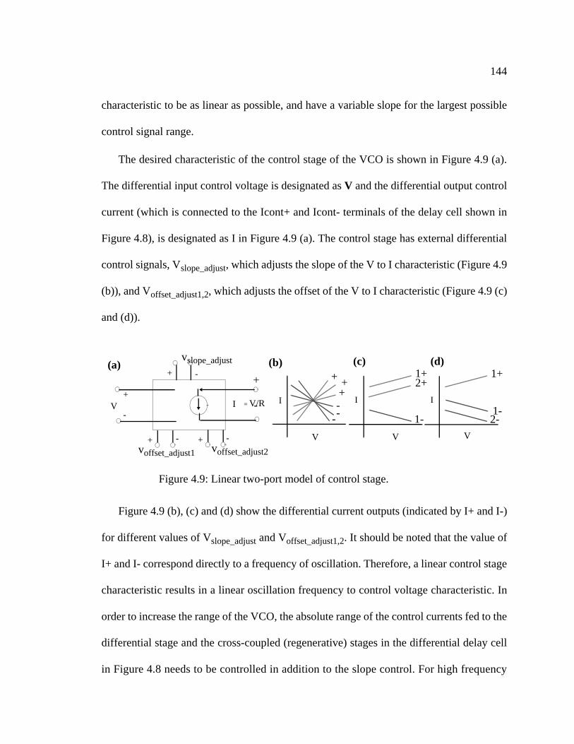
144
characteristic to be as linear as possible, and have a variable slope for the largest possible
control signal range.
The desired characteristic of the control stage of the VCO is shown in Figure 4.9 (a).
The differential input control voltage is designated as V and the differential output control
current (which is connected to the Icont+ and Icont- terminals of the delay cell shown in
Figure 4.8), is designated as I in Figure 4.9 (a). The control stage has external differential
control signals, Vslope_adjust, which adjusts the slope of the V to I characteristic (Figure 4.9
(b)), and Voffset_adjust1,2, which adjusts the offset of the V to I characteristic (Figure 4.9 (c)
and (d)).
Figure 4.9 (b), (c) and (d) show the differential current outputs (indicated by I+ and I-)
for different values of Vslope_adjust and Voffset_adjust1,2. It should be noted that the value of
I+ and I- correspond directly to a frequency of oscillation. Therefore, a linear control stage
characteristic results in a linear oscillation frequency to control voltage characteristic. In
order to increase the range of the VCO, the absolute range of the control currents fed to the
differential stage and the cross-coupled (regenerative) stages in the differential delay cell
in Figure 4.8 needs to be controlled in addition to the slope control. For high frequency
+
-V I = V/R
Figure 4.9: Linear two-port model of control stage.
vslope_adjust
voffset_adjust1
+ -
+ - V
I I
V
(a) (b) (c)
+
-
1+2+
1-
+ ++---
voffset_adjust2+ -
I
V
1+
1-2-
(d)

145
operation, I+ and I- (corresponding to Icont+ and Icont- in Figure 4.8) should be separated
as shown in Figure 4.9 (c) and (d). Voffset_adjust1,2 adds current independently to I+ and I-,
controlling the absolute range of their excursion, and enabling a wide-range of operation
of the VCO.
The class of circuits that we are interested in are called Linear voltage-to-current
Converters (LVICs) . Several LVICs have been reported in the l i tera ture
[145][146][147][148]. Huang [148] reports a low-voltage CMOS LVIC, with a rail-to-rail
input range and single-ended control for adjusting the transconductance of the circuit. This
circuit is modified to increase its tunable range, and is used as the core of the desired
control circuit of the VCO.
The LVIC core shown in Figure 4.10 implements a linear VI conversion such that the
relationship between the difference of I1 and I2 is proportional to the difference between
V1 and V2. Transistors M7 and M8 implement a voltage divider as long as they are
operating in saturation, that is, V1 > 2Vtn, where Vtn is the threshold voltage of the NMOS
M1 M2
VB VBV1 V2
I1 I2
Figure 4.10: V-I Converter core [148]
M3
M4
M5
M6
M7
M8
M9
M10
V1/2 V2/2

146
transistors M7 and M8. Since the same current flows in M7 and M8, their gate-to-source
potential (neglecting the body effect) is the same, implying that the source voltage of M7
and M9 is equal to half the input voltage, that is, V1/2 and V2/2 respectively. The
transistor pair M5-M6 and M3-M4, level-shift up the gate-to-source voltage of M10 and
M8, so that transistors M1 and M2 are functioning at a gate-to-source voltage of Vdd-VB
above the respective gate-to-source voltage. All PMOS transistors have their body
terminals tied to their source terminals. Since the transistors M3-M4 and M5-M6 have the
same current flowing in them, the gate-to-source voltages of transistors M3, M4, M5 and
M6 are equal and have a value of Vdd-VB. The equations for I1 and I2, assuming a naive
level-3 analytical MOS model for analytical simplicity, are as follows:
(4.4)
(4.5)
(4.6)
where Kn = µnCoxW/L. µn, Cox, W and L are the mobility, the gate capacitance per unit
area, the width and the length of the NMOS transistor.
The difference between the currents I1 and I2 is linearly dependent on the difference
of the input voltage and can be tuned by the potential VB. This relationship is valid only as
long as both input voltages V1 and V2 are > 2Vtn. In order for the voltage-to-current
conversion to occur linearly over the desired rail-to-rail input range, the input voltage
dividers composed of transistors M7-M8 and M9-M10 in Figure 4.10 are supplemented by
a complementary divider as shown in Figure 4.11. Transistors M11 and M12 form the
complementary divider of transistors M7-M8 in Figure 4.10. This is converted into a
I1Kn
2------
V1
2------ Vtn–
2 Kn
2------
V2
2------ VDD VB– Vtn–+
2
+=
I2Kn
2------
V2
2------ Vtn–
2 Kn
2------
V1
2------ VDD VB– Vtn–+
2
+=
I2 I1–Kn
2------ V1 V2–( ) VDD VB–( )=

147
current through the differential pair M15-M16 and the load device M18, and is mirrored
through M19. VB compensates for the mobility difference of the NMOS and PMOS
transistors. I1 in Figure 4.11 supplements the current drawn by transistor M7 and M2 in
Figure 4.10. The transistor core of M1-M6 functions correctly even when the voltage
drops below 2Vtn. If the input voltage is below 2Vtn, the current that is drawn by the
voltage divider M7-M8 in Figure 4.10 becomes sub-threshold, at which point the
complementary voltage divider in Figure 4.11 takes over.
The complete schematic of the LVIC core is shown in Figure 4.12. The linear current
response is encoded in the difference of I1 and I2. In order to generate linear differential-
current signals at the output of the LVIC core, Ip and In are mirrored using PMOS
transistors and NMOS transistors as shown in Figure 4.13. The differential signals Ip - In
and In - Ip are then easily obtained as currents. For large slope-variation with input voltage
and change in VB, transistors M3 and M5 in Figure 4.12 are biased in the linear region of
operation, which has a larger Ids-Vds slope than the saturation region.
Figure 4.11: Voltage divider complement of M7-M8 in Figure 4.10
VB
V1/2V1M11
M12
M13
M14
M15 M16
M17
M18 M19
I1

148
The dc-current output difference Ip-In of the LVIC for different input differential
voltages with a bias of 1.8 V are shown in Figure 4.14 (a) for 80 °C and the slow process
corner library model decks. The slope of the current difference output (Ip-In) changes in
different directions for large positive or negative differential input voltage depending on
the value of VB. As VB increases, the gate-to-source voltage of M3 and M5 decreases,
resulting in the transistors moving in and out of the linear region over the input dynamic
M1 M2
VB VB
V1 V2
I1 I2
Figure 4.12: Complete rail-to-rail V-I converter core (load devices not shown).
M3
M4
M5
M6
M7
M8
M9
M10
VBVB
Figure 4.13: Differential linear voltage-to-current converter (LVIC).
IpIn
I po
- Ino
InoIpoI n
o - I
po
V+ V-
VB
MPLp MPLn

149
range. The gate-to-source voltage variation of M1 and M2 in Figure 4.12 for large VB has
two slopes: one corresponding to the linear region and the other corresponding to the
saturation region. This results in two breakpoints (large VB kink in Figure 4.14) in the Ip-
In versus differential input voltage curve shown in Figure 4.14, for VB=2.0V, each
corresponding to the movement of M1 (M2) from the linear region, which has a larger Ids-
Vds slope, to the saturation region, which has a smaller Ids-Vds slope. This can be partially
solved by reducing the size of transistors M3 and M5 in Figure 4.12, which reduces the
variation in slope that can be achieved by changing VB.
For small values of VB (in the range of 0 V to 1 V), the drain-to-source voltage of M3
and M5 in Figure 4.12 are near the positive supply, causing both M1 and M2 to draw
larger current than they would for large values of VB. This causes the drain-to-source
voltage of the diode-connected PMOS transistor load devices (for example, MPLp and
MPLn in Figure 4.13) to increase, compressing the drain-to-source voltage of the voltage
divider circuits M7-M8 and M9-M10 in Figure 4.12. The gate-to-source voltage of M8
and M10 are then less than the desired value of half the input voltage (gate voltage of M7
and M9 respectively), typically over part of the input dynamic range when the input
voltage is large (for example > 2 V). The “breakpoint” depends on the size of the load
device and is shown as the low VB kinks in Figure 4.14. Note that this occurs
asymmetrically, that is, as the gate-to-source voltage of M10 decreases from the ideal
value of V2/2, the gate-to-source voltage of M8 is not affected as V1 is small. This causes
a further difference between the output currents for large differential voltages as shown in
Figure 4.14 for VB = 0 V. Note that the change in slope has decreased for VB = 1V.

150
Figure 4.14 (b) shows that the variation in slope of the LVIC output due to change in
temperature from 25 °C to 80 °C is fairly small. The breakpoint (low VB kink) problem
can be solved by increasing the size of the diode-connected PMOS load transistor.
Arbitrarily increasing the size of the diode-connected load transistors MPLp and MPLn in
Figure 4.13, will cause the mirror transistors to operate in deep saturation. The large VB
kink problem can be solved by reducing the size of transistors M3 and M5 in Figure 4.12.
This causes the drain-to-source voltage variation of M3 and M5 for low VB to be larger,
thus increasing the slope if the Ip-In versus input differential voltage curve for the same
VB. This reduces the change in slope that can be achieved by adjusting VB. Since we
desire to operate the VCO with low gain (that is, small VB in control circuit) in most
applications, the change in slope for large VB is not considered to be a critical problem.
Figure 4.14: Current output of LVIC in Figure 4.13 (a) for different slope controlvoltages and for (b) 25 °C, 45 °C, and 80 °C for VB = 1V.
VB=0V
VB=1V
VB=2V
Differential control voltage (V+-V-) Differential control voltage (V+-V-)
25 °C
80 °C
(a)(b)
Low VB kink
Low VB kink
Large VB kink
Large VB kink

151
Since decreasing VB causes the core transistors M1 and M2 in Figure 4.14 to consume
significantly more current, the voltage divider circuitry and the core circuitry are
separated. The voltage divider circuits (shaded area in Figure 4.14) are separately
connected to the supply through diode-connected PMOS transistors. Transistors M1 and
M2 are connected to wide diode-connected PMOS transistors so that for low VB, more
current can be drawn and a lower slope of Ip-In can be realized. The modified schematic of
the linear voltage-to-current schematic is shown in Figure 4.15. The output of the voltage
divider circuitry (the gate-to-source voltage of M8 and M10) is shown in Figure 4.16 for
VB=0.0 V, 1.0 V and 2.0 V for input differential voltage from -1.8 V to +1.8 V. The finite
voltage drop across the load device introduces a small fixed slope error, but linearity is
preserved over the input dynamic range. Figure 4.17 (a) shows the arithmetic difference
between the currents Ip and In in Figure 4.15, and the current output using the subtractor
M1 M2
VB VB
V1 V2
I1 I2
Figure 4.15: Modified rail-to-rail VI converter core (load devices not shown).
M3
M4
M5
M6
M7
M8
M9
M10
VBVB
InIp

152
circuit shown in Figure 4.13 (b) for VB = 0.0 V, 1.0 V and 2.0 V. It can be seen that
linearity is preserved in all three cases, and that better than 1:4 variation in output slope is
realized.
Figure 4.18 (a) and (b) show the temperature variation of the linear voltage-to-current
output of the LVIC core and the output of the subtraction circuit respectively, for VB =
1 V at temperatures of 25 °C, 45 °C, and 80 °C. The subtractor circuit is responsible for
Figure 4.16: Gate-to-source voltage of transistors M8 and M10 in Figure 4.10 forrevised LVIC.
Differential control voltage (V+-V-)
Vc- Vc+
Figure 4.17: (a) Ip-In and (b) Ipo-Ino for the revised LVIC for VB=0 V, 1.0 V and2.0 V.
(a) (b)
Differential control voltage (V+-V-) Differential control voltage (V+-V-)
VB=2.0V
VB=1.0V VB=0.0V
VB=2.0V
VB=0.0VVB=1.0V

153
the downward shift of the curve with increasing temperature. The LVIC core in Figure
4.15 has very little variation with temperature, as can be seen in Figure 4.18 (a).
The offset-adjustment circuitry in Figure 4.9 is implemented using two PMOS
differential pairs (M14-M18 and M19-M23) as shown in Figure 4.19. The current output
of M21and M16 is added to Ip - In and In - Ip respectively, through transistors M22 and
Figure 4.18: (a) Ip-In and (b) Ipo-Ino for revised LVIC for temperature of 25 °C,45 °C, and 80 °C.
(a) (b)
Differential control voltage (V+-V-) Differential control voltage (V+-V-)
25 °C
80 °C
Figure 4.19: Differential linear voltage-to-current converter with offsetadjust circuitry. VB is the slope control.
Ip In
I po
- Ino
InoIpo
I no
- Ipo
V+ V-
VBM14
M15M16
M17M18
M19
M20 M21
M23 M22
Voffset_adjust1 Voffset_adjust2
Vcntrl+ Vcntrl-
vbias vbias

154
M18. The control signal then becomes a voltage, which is distributed to the differential
delay cells. The delay cells in Figure 4.8 have transistors M7 and M8 removed, as they are
equivalent to transistors M22 and M18.
4.2.3 Jitter Sources in Ring Oscillators:
The following are some of the noise sources in ring oscillators:
1. Thermal noise in the delay-cell load
2. Thermal noise of the tail-current sink of the differential pair
3. Sampling of thermal noise at the delay cell inputs
4. Regenerative switching
5. Power-supply noise
6. Substrate noise
7. Signal history
8. Mismatch between the delay cells due to process variations
9. Thermal gradient across the oscillator
10.Non-uniform load at output of the delay cells
11.Noise in the control signals
Thermal noise due to the load devices at the output of each delay cell appears directly
at the output of the delay cell. This noise is bandlimited by the poles at the delay cell
output. Tail-current sink noise is always present in a differential circuit. In usual operation
when the stage operates as a balanced differential circuit, the tail-current noise appears as
a common-mode signal at both outputs and is absent as a differential signal. When the
differential delay cell is in operation, the outputs are switched on and off -- i.e., one of the

155
outputs has all the tail-current and the other has none when the delay cell has finished
switching. At this point, the tail-current noise current appears fully at the output
corresponding to the input device that is fully turned on. In MOS differential delay cells,
the tail-current sink noise current is dominated by the channel thermal noise.
The noise sources at the output of the preceding delay cell become input noise sources.
When the noise input to the differential stage is at the gate of the input stage transistors,
the input noise sources can be viewed as noise voltage sources. When the delay cell
switches and passes through its active region, the input noise voltage is converted to
output noise current by the differential pair which is integrated onto the load capacitances
of the differential output stage.
Regenerative switching influences the behavior of the differential delay cell by
making the time at which the switching occurs more uncertain. The reason this occurs is
because during switching, the gain of the regenerative pair becomes very large, and the
input noise, which is multiplied by this large gain, gets translated to the output.
Signal history leads to a situation where the history of the jitter of each stage affects
the jitter in the next time segment. This occurs when the output load is modeled as an RC
load, and the period of the oscillation is not long enough to fully charge or discharge the
load. If the output does not settle to its final value, any delay error until the next switching
results in a correlated-delay error in the delay of the delay element, which increases the
jitter. This means that the jitter penalty due to non-uniform delay cell output waveforms is
higher because of this mechanism. This implies that the rise- and fall-times of the delay
cells must be as symmetric as possible to reduce the impact of signal history. As the

156
number of stages increases, this effect diminishes because the waveforms have adequate
time to settle close to the maximum or minimum values (> 6 time constants). Lin et al.
[140] discusses the use of diodes as a clamping mechanism to make sure that at the time
the delay cell switches, the waveforms are always at the same initial condition,
independent of previous delay errors. This effect can also be minimized by ensuring that
the delay cells have large slew-rate outputs so that they are not RC time-constant limited
and by making sure that the output of each delay cell is equally loaded.
The influence of power-supply noise manifests itself as a modulation of the delay cell
waveform. Its presence can be seen as sidebands close to the carrier or oscillation
frequency when the waveform is analyzed using a spectrum analyzer [141]. This “spur”
noise increases the time-jitter of the oscillator output. Power-supply noise is converted
into a noise current in parallel with the tail-current sink of a differential delay cell by
integration across the parasitic capacitor in parallel with the tail-current sink. This appears
as a common-mode signal during differential operation, but when the outputs are fully
switched, this noise appears fully at the switched output whose driving transistor carries
all the current. Power-supply noise effects can be minimized by isolating the power
supplies of the oscillator and decoupling them separately from the power supply of the rest
of the circuitry, implementing at least bond-wire isolation, if not isolation to the board by
a separate power plane on the package. Additionally, power-supply decoupling circuitry
can be added to the delay cell, which decouples the capacitance across the tail-current sink
through a low-impedance path to the supply node. However, this method does not protect
the delay cell from noise on the node with the lowest potential.

157
The influence of substrate noise is similar to that of power-supply noise. The substrate
noise has to be made as minimal as possible by using a guard ring close to the oscillator,
returned to ground via a separate bond wire from the rest of the circuitry. The noise
generating circuitry has to be made as quiet as possible. In advanced CMOS processes
with low-resistivity bulk p-substrates, the digital circuitry should have minimal substrate
contacts tied to the ground connection of digital circuitry. The digital circuit substrate
should be separately returned to ground through a low impedance path. This avoids latch-
up in digital circuitry. Additionally, the backside of the IC should have an ohmic contact
for a low-inductance return path [142] for the substrate current to the cavity bottom, which
should be package ground.
The mismatch in delay cells can be minimized by symmetrical interleaved layout
techniques, which reduce the impact of spatial variations of transistor parameters across
the wafer. Dummy devices are used to provide the outer transistors the same environment
as the inner transistors. The oscillator is oriented so that all the delay cells see the same
thermal gradient due to high-power circuit blocks from other parts of the IC.
This is not always possible as it might conflict with the symmetrical layout
requirements of the oscillator. A non-zero thermal gradient across the oscillator is
equivalent to the effect of process variations in that it will result in slightly hotter delay
cells to be slower than delay cells which are at a lower temperature. In oscillators with a
small number of delay cells, this effect is likely to be small because of the small physical
area occupied by the delay cells, and the consequent small thermal gradient across that
area.

158
The oscillator layout has to be such that the delay-cell outputs have exactly the same
load capacitance. The node with the maximum capacitance sets the pole of the oscillator
or the frequency at which the oscillation occurs. The different RC time-constants at each
node manifests as jitter via mechanisms similar to signal history.
The control signal that controls the delay of each delay cell, and hence, the frequency
of oscillation, is a port through which noise can influence the time jitter of the oscillation.
A fully differential control and delay path is essential to achieve a low-jitter oscillator, and
hence, a low-jitter PLLFS.
4.2.4 VCO Measurements
The schematic of the oscillator that was simulated, fabricated, and measured is shown
in Figure 4.20. The shaded block is the actual ring oscillator composed of three
differential delay-cells shown in Figure 4.8. As most of the delay-cell current starts
out1
out2 out3ControlCircuit
oscillator
differentialcontrolsignals
offsetadjust1
offsetadjust2
control voltageslope adjust
Figure 4.20: Schematic of VCO and control circuit that is simulated, fabricated andmeasured.
(Figure 4.19)
(Figure 4.8)

159
flowing in the cross-coupled (regenerative) pair of the differential delay-cell, the stage
begins to distort the output waveform as shown in Figure 4.21 (a). The upper waveform is
the output of a differential delay cell in the oscillator at 200 MHz. The distortion is
“cleaned up” by passing it through a buffer, which is identical to the VCO delay stage and
controlled in the same manner by the control circuit in Figure 4.20. This enables the buffer
to behave as a comparator and clean up the distorted oscillator waveform. This distortion
occurs in the oscillator because the range of the VCO is being extended to the lower end of
the frequency range, by steering enough current into the regenerative section of the delay
cell, to slow down the delay cell such that its latch characteristic comes into play. The
distortion occurs because of an effect similar to kickback noise [80] in high-speed CMOS
comparators. As the input to the delay cell switches, the cross-coupled pair M3-M4 in
Figure 4.8 is forced to switch after the delay of the cell. The gain of the cross-coupled pair
is high enough that the source of the input differential pair M1-M2 tries to follow the
cross-coupled pair through whichever transistor of the input differential pair M1-M2 is on.
This switching action temporarily increases the potential at the source of the input
differential pair M1-M2, increasing the rise- and fall-time of the output waveform for the
duration of the switching time, resulting in the distortion. Another way of looking at this
phenomenon is that the current in the on transistor of the input differential pair M1-M2
(which has already “switched”, but lacks enough current to fully switch the output of the
delay cell) increases at the onset of the switching of the cross-coupled pair (speeding up
the fall), then decreases as the source voltage of input differential pair M1-M2 increases,
and decreases even further as the cross-coupled pair switches completely (the transistor in

160
the cross coupled pair which switches from off to on, shares its drain with the transistor in
the input differential pair M1-M2 that is on). Thus, a ringing behavior is seen in the
current flowing through the on-transistor in the input differential pair M1-M2, which leads
to the distortion in the falling edge output waveform. As the gain of the cross-coupled pair
increases, the switching current waveform in the cross-coupled pair becomes more and
more non-linear, distorting the rising edge output of the differential delay cell. The
distortion increases as more current flows through the cross-coupled pair and less current
through the input differential pair. Thus, unlike traditional ring oscillator delay elements
whose noise mechanisms result in a monotonic increase of jitter with frequency of
oscillation, this oscillator is likely to have higher jitter at the lower end of the frequency
range in the extended range configuration. This is a fundamental source of jitter in this
delay cell and cannot be avoided because of the reliance on the regenerative pair.
However, since the low end of the frequency range of the VCO is used only for testing
purposes and the period of the clock is large, larger jitter at lower frequencies than at
higher frequencies is easily tolerated.
The distortion of the output of the differential pair can be compensated by making the
output buffer at each node of the oscillator behave as a differential delay cell which is
designed to have more standby current (i.e., a larger transistor M6 in Figure 4.8). The
cross-coupled pair’s gain is weaker than that of the delay cell in the ring oscillator and
cleans up the output of the oscillator as shown in the lower panel of Figure 4.21 (a). At
higher frequencies, the cross-coupled pair in the buffer should have little, if any current, as
it would slow down or distort the output. This is the rationale for designing the buffers

161
along the same lines as the differential delay cell, with slightly different standby current
specifications in the input differential pair M1-M2. The performance of the ring oscillator
and the buffer output at 1.25 GHz is shown in the top and bottom panels respectively, in
Figure 4.21 (b), showing no adverse effects of regenerative behavior (required for low
frequencies) in the buffer. All simulations have been done using the slow process corner
library decks at a junction temperature of 80 °C.
A testdie photograph (T6) with a VCO designed to have a range of 0.2 to 1.6 GHz,
using the slow libraries of the 0.5 µm HPCMOS14TB process, is shown in Figure 4.22.
The VCO is a three-stage ring oscillator with differential delay cells shown in Figure 4.8
without decoupling circuitry. Each node is equally loaded with buffers that can drive
electrical LVDS transmitter circuits capable of operating at a maximum data rate of 3.3
Gb/s while driving a 50 Ω load (Section 3.10 on page 114). The testdie has noise
oscoutput
bufferoutput
oscoutput
bufferoutput
latch induceddistortion
(a) (b)
Figure 4.21: Simulated waveforms of the oscillator output at (a) 215 MHz and (b)1.25 GHz using the slow process corner library decks at a junction tem-perature of 80 °C.

162
generation circuitry and has the control circuit laid out so that its dc- and ac-performance
can be independently tested from the oscillator.
The noise generation circuitry included on the IC is in the form of two single-ended
current-starved tunable VCOs driving on-chip, digital Transistor-to-Transistor (TTL)
pads. The power supply of the noise generation circuitry, which includes the digital TTL
driver with 2 ns rise- and fall-times, is directly connected to the power and ground nodes
of the VCO, control circuit, and prescaler circuitry. The TTL output pad pre-drivers have a
separate power pad called nsvdd, which also supplies power to one of the noise
oscillators. This enables or disables the TTL pads. The noise generation circuitry has two
single-ended oscillators, ni1 and ni2, with frequency range from 600 MHz to 950 MHz.
Testdie (T6) to measureperformance of the VCO andcontrol circuit. The IC measures2.17 mm x 2.0 mm. Accountingfor the bypass capacitors, theVCO occupies 354 µm x 293 µm,the control circuit, 173 µm x 149µm.
Figure 4.22: Layout of Testdie (T6) to test VCO without decoupling circuit.
1x6
LV
DS
Tra
nsm
itter
Arr
ay
VCO and Buffers
VC
O C
ontr
olC
ircu
it
Con
trol
Cir
cuit
test
pad
s
VCO Control Circuit
Noise Generation Circuitry

163
ni1 was designed to be operational only when the power and ground supplies of the noise
oscillator are connected. However, substrate contacts in the oscillator are able to provide
the ground connection for the oscillator, enabling operation when only power is provided.
ni1 is therefore, always on, injecting power, ground and substrate noise into the VCO
circuitry under test. ni2 is designed to inject noise only into the substrate node of the VCO
under test. During measurements, the control voltage of the noise oscillator was set to 0 V.
The noise generation circuitry selectively allows the following tests:
• VCO test under noise injection conditions from one single-ended oscillator only,
in close proximity, whose power supply is shared by the VCO under test. This
simulates the presence of logic circuitry on the IC. Noise injection occurs into the
power, ground, and substrate nodes.
• VCO test under additional noise injection into the substrate node, by a second
single-ended oscillator located in close proximity to the first noise oscillator. This
oscillator is designed to add only substrate noise to the VCO under test.
• Test of a passive noise isolation mechanism. This test structure is a guard ring
composed of a substrate contact ring around noise oscillators with a separate return
path to ground. An error in layout on the IC forces the incision3 of the ground
connection of the TTL pads, to test the impact of substrate noise injection alone by
measuring the increase in jitter when the second oscillator is turned on over the jitter
induced by the first oscillator (which is always on).
3. The layout allows relatively easy incision by using a passive probe on a probestation. The connection to be incised is on top level metal and is separated fromits nearest neighbor by 25 µm.

164
The noise oscillator is a three-stage ring oscillator composed of delay cells whose
schematic and symbol are shown in Figure 4.23. The delay is composed of two inverters
in parallel, one of whose delay is controlled by interposing PMOS and NMOS transistors
acting as current sources and sinks between the switching transistors and the supply nodes.
Variation of the magnitude of the current source and sink is achieved by changing the gate
voltage of the appropriate transistor by changing signals cntrlp and cntrln together. Signals
cntrlp and cntrln are derived from a single-ended external control signal by a current-
mirror circuit shown in Figure 4.24.
The output of the oscillator is divided by a cascade of six toggle flip-flops connected
in a ripple counter fashion, which divides the output of the noise oscillator by 26. Each
toggle flip-flop is a modified form of the 9 transistor TSPC toggle flip-flop reported in
[88]. The schematic and symbol of the toggle flip-flop are shown in Figure 4.25. The
modification interchanges the positions of the PMOS transistors in the first set of series-
connected transistors so that the load seen by the clock input is lower. A better
optimization has been reported in [173], where the same idea is applied to the NMOS
transistors in the last set of series-connected transistors in Figure 4.25.
Figure 4.23: Schematic and symbol of delay cell of single-ended oscillator.
cntrlp
cntrln
in out
cntrlp,n

165
The schematic and symbol of each noise oscillator are shown in Figure 4.26. The
maximum noise component is the contribution from the output driver of the oscillator
driving the node out, whose frequency is one-sixty-fourth the noise-oscillator frequency.
The schematic of the interaction paths of the VCO under test and the noise oscillators is
shown in Figure 4.27.
Figure 4.24: Schematic and symbol of noise-oscillator control circuit.
vco_cntrl
cntrlp
cntrln
cntrlp
cntrln
vco_cntrl
φ
φφQ
Qφ
1/2
Figure 4.25: Schematic and symbol of toggle flip-flop used to divide the out-put of the single-ended oscillator.
Figure 4.26: Schematic and symbol of single-ended noise oscillator.
cntrlp,n cntrlp,n cntrlp,ncntrlp
cntrln
vco_cntrl
Q1/2
Q1/2
Q1/2
Q1/2
Q1/2
Q1/2
out
vco_cntrl out

166
Blocks ni1 and ni2 are the two noise oscillators whose schematic is shown in Figure
4.26. ni1 shares the power and ground of the VCO under test along with ground node of
the TTL output pads. ni2 has both power and ground connections enabled externally by
nsvdd and nsgnd. nsvdd also controls the power of the TTL pad pre-drivers so that
turning off nsvdd will turn off both TTL pads and ni2. The interaction of ni1 and ni2 can
be seen by looking at the jitter histogram of the output of either ni1 or ni2. The power
supply voltage was set to 3.3 V and the control voltage of the noise oscillators was set to
3.3 V for maximum frequency of oscillation.
VCOunder test
VCO_VDD
VCO_GND
nsvdd
nsgnd
TTL PAD
TTL PAD
guard_ring
noiseoscillatoroutput1
noiseoscillatoroutput2
Figure 4.27: Schematic showing interaction of VCO under test with noise oscillatorcircuitry through power and ground connections.
ni1
ni2

167
Since ni2 gets its ground connection from the substrate if nsgnd is floating, we look at
the jitter histogram of the output of ni1when both oscillators are running. The TTL output
of ni2 is not connected to the scope and is left floating to minimize the interaction through
the TTL driver. Figure 4.28 shows the jitter histogram of ni2 at 14.83 MHz (which is 1/64
of 950 MHz, the maximum output frequency of the oscillator) when nsgnd in connected
(a) and disconnected (b). The jitter histogram is bimodal indicating two separate noise
sources, corresponding to the noise sources ni1 and ni2. Additionally, the measured
frequency of oscillation ni1 and ni2 differ by about 10% due to differences in the power
supply impedances and process variations across the die. When the ground of ni2 is
connected (by connecting nsgnd to ground), the jitter is higher than when it is
disconnected (Figure 4.28 (b)). This is possibly due to the two ground return paths for ni2:
one through the substrate and then the ground connection of ni1, and the other through its
(a) (b)
Figure 4.28: Jitter histogram of ni1 at 14.83 MHz (950 MHz) with (a) nsgnd con-nected showing 49.24 ps rms jitter (240 ps peak-to-peak) and (b)nsgnd disconnected, with 46.53 ps rms jitter (200 ps peak-to-peak).The horizontal scale is 200 ps/div and the vertical scale is 100 mV/divfor both (a) and (b).
100
mV
/div
100
mV
/div

168
own ground return path, which is more inductive because it is returned to ground through
a signal line on the package and the test fixture board.
A testdie (T8) with the above VCO driving prescalers, designed to have a frequency
range from 200 MHz to 1.6 GHz using the slow process corner libraries of the 0.5 µm HP-
CMOS14TB process at a junction temperature of 80 °C, was fabricated and measured.
The corresponding die photograph is shown in Figure 4.29. The VCO is a three-stage ring
oscillator composed of the differential delay cell in Figure 4.8 and the control circuit in
Figure 4.19. The VCO has buffers on each delay stage output, two of which directly drive
electrical LVDS transmitters capable of operating at a data rate of 3.3 Gb/s while driving a
50 Ω load (Section 3.10 on page 114).
Testdie (T8) to measureperformance of VCO, 4/5, 4/5/6and 4/6 prescalers in 0.5 µmCMOS techno logy . The ICmeasures 2.15 mm x 2.5 mm.Accoun t ing fo r t he bypas scapacitors, the VCO occupies354 µm x 293 µm, the controlcircuit, 173 µm x 149 µm. The 4/5 prescaler occupies 213 µm x700 µm, the 4/5/6 prescaleroccupies 286 µm x 700 µm andthe 4/6 prescaler occupies 215µm x 700 µm. Each prescaler hasan output buffer which occupiesan area of 105 µm x 273 µm.
Figure 4.29: Die photograph of T8 (VCO and prescaler test IC).
1x5
LVD
S T
rans
mitt
er A
rray
Noi
se G
ener
atio
nC
ircu
itry
4/5 prescaler
4/5/6 prescaler
4/6 prescaler
VC
O +
Buf
fers
Clockbuffers
VCOControlCircuit

169
The VCO also drives an array of four clock buffers which occupy an area of 336 µm x
433 µm. These clock buffers drive three prescalers which occupy the right half of the IC.
The prescaler designs in Figure 3.15 (4/5 prescaler), Figure 3.17 (4/5/6 prescaler) and
Figure 3.19 (4/6 prescaler) are designed to run at 1.6 GHz at a junction temperature of
85 °C using the slow process corner model decks of the 0.5 µm HP-CMOS14 process. The
outputs of each divider are observed using electrical LVDS transmitters. The output of
each prescaler is buffered prior to driving the LVDS transmitter by a buffer which
occupies an area of 105 µm x 273 µm. The LVDS transmitters are laid out in an array and
have their power supplies isolated by bond-wires from the oscillator and prescaler power
supplies.
The performance of a VCO can be measured in the frequency or the time domain.
Frequency-domain measurements involve measurements on a spectrum analyzer which
give the phase-noise Power Spectral Density (PSD), which when normalized to the carrier
or fundamental frequency power, gives the power spectrum, Sf(f), of the phase jitter
process [170]. There are a number of measures in the time domain. The most common one
is the two-sample standard deviation of the distribution of times between the threshold
crossings of a trigger and input waveform. This standard deviation does not converge in
the presence of nonstationary noise processes with frequency characteristic 1/fn, when n >
2 [174]. A number of time-domain jitter measures have been developed to deal with these
issues which are robust but require complicated instrumentation [175]. The two-sample
standard deviation measure is used here because of its simplicity and sufficient accuracy.
A trigger waveform and the waveform whose jitter measure is to be measured are fed into
170
a Communications Signal Analyzer (CSA). The CSA compiles a histogram of the
threshold crossings of the input waveform that occur in a time window defined at a delay,
called the timebase, after the trigger transition. The standard deviation of this histogram is
the time-jitter measure of the input waveform.
The performance of the VCO is measured using the two-sample standard deviation
measure by a Tektronix 803A Communications Signal Analyzer (CSA) [176]. The jitter
measurements are either self-referenced or source-referenced measurements. The
condition for validity of this measurement is that there is no drift in frequency during the
time it takes to compile the jitter histogram [170]. Both the CSA and the IC are powered
up for two to three hours prior to measurements. The immediate thermal environment is
approximately at the same temperature during the measurement process. The accuracies of
the CSA 803A are typically 1.3 ps rms + 4 ppm of position (typical) and 2.0 ps rms + 5
ppm of position (maximum). Most of the VCO measurements are at the measurement
floor of the CSA 803A. The trigger level is adjusted to be in the middle of the range prior
to initiating a jitter measurement. The jitter histogram is compiled until it reaches steady
state -- i.e., there is minimal change in the peak-to-peak and rms jitter measurements as the
number of points increases. This usually takes a few minutes. For best results, the slope
error of the waveform must be avoided, otherwise an apparent increase in the measured
jitter is seen. The least jitter is obtained when both the trigger and input waveform are
unattenuated and the vertical resolution is set to the smallest value. The input waveforms
amplitude must be less than the maximum magnitude that the sampling scope head can
tolerate.
171
The jitter measurements are made in the presence of noise injected by a single-ended
VCO into the power, ground and substrate nodes of the differential VCO and its control
circuit under test. The T8 VCO has power supply noise decoupling circuitry in each
differential delay cell (though not in the VCO output buffers). The jitter measurements are
done at the smallest possible timebase setting. This is because the measured self-
referenced jitter of a VCO monotonically increases with the oscilloscope time base
setting, as the VCO integrates frequency to get phase for which there is no limit -- i.e., as
time goes to infinity, the phase error goes to infinity. Figure 4.30 (a) and (b) show the
measured self-referenced jitter and the spectrum analyzer measurement, respectively, at
the highest frequency of the VCO. The measured self-referenced rms jitter is 4.46 ps. This
measurement improves to 3.76 ps (rms) when the waveform slope-error is diminished by
removing the attenuation on the input waveform and on the trigger input. Although not
pursued here, the low-frequency and high-frequency jitter components of the VCO could
possibly be determined from an analysis of the structure of the power spectrum [177]. This
method considers the ratio of the power of the carrier to the power of the various noise
bands, and the Full-Width at Half-Maximum (FWHM) of the noise bands, at different
resolution bandwidth settings on the spectrum analyzer. Figure 4.30 (a) shows the self-
referenced jitter histogram and Figure 4.30 (b) shows the spectrum analyzer output of the
VCO at 1.7 GHz with noise source ni1 active. The self-referenced jitter is measured to be
4.46 ps rms (35 ps peak-to-peak) at 1.7 GHz. Figure 4.31 (a) shows the self-referenced
jitter histogram and Figure 4.31 (b) shows the spectrum analyzer output of the VCO at 123
MHz with noise source ni1 active. The self-referenced jitter is measured to be 70.73 ps

172
rms (420 ps peak-to-peak) at 123 MHz. Examination of the power spectrum of the VCO
outputs at 123 MHz and at 1.7 GHz indicate that there are stronger noise bands at 1.7 GHz
than at 123 MHz.
(a) (b)
Figure 4.30: (a) Jitter histogram (self-referenced) of 1.7 GHz VCO output after 20dB attenuation showing jitter of 4.46 ps rms (35 ps peak-to-peak). Thehorizontal scale is 50 ps/div and the vertical scale is 2 mV/div. (b) Spec-trum analyzer output for 1.7 GHz output of T8 VCO with noise sourceni1 active.
2 m
V/d
iv
(b)(a)
2 m
V/d
iv
Figure 4.31: (a) Self-referenced jitter of 123 MHz VCO output with 70.73 ps rms(420 ps peak-to-peak). The horizontal scale is 200 ps/div. (b) Spectrumanalyzer output of 123 MHz oscillation of T8 VCO. The noise sourceni1 is active for both (a) and (b).

173
The T8 VCO was investigated under seven settings which covered the desired range
but were by no means exhaustive. The impact of slope variation on jitter by adjusting VB
is discussed in Section 4.6 on page 201. As expected, it is seen that the self-referenced
VCO jitter increases as VB increases, due to the fact the VCO becomes more sensitive to
noise as the VCO gain Ko increases. The details of the settings are listed in Table 4.1.
Signals Vy1p and Vy1n correspond to Voffset_adjust1 in Figure 4.9, signals Vy2p and Vy2n
to Voffset_adjust2 in Figure 4.9, and signal VB to Vslope_adjust in Figure 4.9. The input
differential voltage to the VCO was varied from 0 V to 3.6 V, as a differential voltage
variation of -1.8 V to +1.8 V centered at 1.8 V. Table 4.1 also lists the measured frequency
range for each setting and the calculated oscillator gain Ko in Gigarads/sec-Volt (Grad/
sV). Signals Vy1p,n and Vy2p,n are differential voltages centered at 1.2 V. VB is
arbitrarily fixed at 1.0 V for all settings, and has a designed range of 0.0 V to 2.0 V.
Setting Vy1p (V)
Vy1n (V)
Vy2p (V)
Vy2n (V)
VB (V)
Frequency-range (GHz)
Ko(Grad/sV)
Vcntrl (V)
setting1 0.0 1.0 1.0 1.4 1.0 0.962-1.44 0.8343 0-3.6
setting2 0.0 1.0 0.0 2.4 1.0 1.23-1.704 0.8273 0-3.6
setting3 0.0 1.0 2.4 0.0 1.0 0.725-0.824 0.173 0-3.6
setting4 1.4 1.0 2.4 0.0 1.0 0.325-0.640 0.55 0-3.6
setting5 0.5 0.0 2.4 0.0 1.0 0.479-0.707 0.398 0-3.6
setting6 0.0 0.0 2.4 0.0 1.0 0.607-0.778 0.2985 0-3.6
setting7 2.0 0.0 2.4 0.0 1.0 0.123-0.452 0.5742 0-3.6
Table 4.1 Setting descriptions for T8 VCO measurements

174
The measured frequency and self-referenced rms jitter statistics are plotted in Figure
4.32 (a) and (b) respectively, for varying input differential control-voltage. The measured
data covers the VCO range of 123 MHz to 1.7 GHz. The self-referenced rms jitter is under
5.0 ps rms for most settings. The rms jitter increases primarily due to the increase in the
current in the cross-coupled (regenerative) pair in the differential delay cells of the
oscillator. This effect comes into play when the VCO is moved to lower frequency ranges
of oscillation. This behavior can be seen in Figure 4.32.
The self-referenced rms jitter is highest (51 ps) at 123 MHz. This is not significant
because the period of the clock is greater than 8 ns, which can easily accommodate a time
jitter of 51 ps rms (338 ps peak-to-peak). The data for settings 2, 3, 5 and 6 was
remeasured under more accurate jitter measurement conditions mentioned earlier
(unattenuated input, unattenuated trigger, and the smallest possible timebase setting on the
Figure 4.32: (a) Measured T8 VCO frequency and (b) self-referenced rms jittercorresponding to each setting in (a). Note that the on-chip noise sourceni1 is active during the measurements,
(a) (b)

175
CSA) with more data points. The results are plotted in Figure 4.33 (a) for frequency of
oscillation and (b) for self-referenced rms jitter. The jitter histogram in all cases was seen
to have Gaussian statistics. The data again confirm the expectation that jitter increases
rapidly for the very large negative differential input control voltage to the VCO, showing
the domination of the regenerative pair on the jitter statistics. Setting 6, the setting which
has the lowest measured self-referenced jitter (crosses in Figure 4.32 (b)) among the
settings in Table 4.1, is chosen to measure the impact of power-supply and substrate noise
sensitivity.
The measured results are plotted in Figure 4.33, which shows (a) the frequency of
oscillation and (b) the self-referenced rms jitter for three cases:
1. Only ni1 on (default case)
Figure 4.33: Measured T8 VCO (a) frequency and (b) self-referenced rms andpeak-to-peak jitter corresponding to each setting in (a). Note that theon-chip noise source ni1 is active during the measurements.
(a) (b)

176
2. nsvdd = 3.6 V (both noise oscillators ni1 and ni2 on, TTL pads drive only the
transmission line on the package and the PCB), and noise oscillator frequency set to
lowest frequency.
3. nsvdd = 3.6 V and nscntrl = 3.6V (highest frequency of oscillation for both ni1 and
ni2).
Figure 4.34 (a) illustrates the low VB kink problem associated with the VCO control
circuit detailed in Figure 4.14. Figure 4.34 (b) shows the self-referenced rms jitter plots for
the three noise injection scenarios detailed above. The baseline self-referenced jitter (with
on-chip noise source ni1 active) corresponds to the lowest curve (diamonds) in Figure
4.34 (b). It is seen from Figure 4.34 (b) that injecting TTL pad-noise (squares and circles)
directly into the VCO, dramatically increases the VCO jitter, and swamps the noise
Figure 4.34: (a) Measured frequency and (b) self-referenced rms jitter histogramvariation of T8 VCO at setting 3, for different levels of noise injection.The TLL pads are not terminated in measurements.
(a) (b)

177
contribution of ni1 to the VCO jitter. The baseline jitter curve for setting 3 (lowest curve
in Figure 4.34 (b)) increases for differential VCO control voltage < -1.0 V and > 1.0 V.
This increase is due to two effects. One is the increase in slope of the control-circuit
transfer characteristic (Figure 4.34 (a)), which increases the VCO gain, and the other is the
increased current flow in the cross-coupled pair in the delay cell. The almost symmetric
increase in the VCO jitter due to the larger VCO gain for control voltages < ~ -0.6V and >
~1.2 V can be seen from the lowest curve (diamonds) in Figure 4.34 (b). We conclude
from the symmetric nature of the curve that the jitter contribution from the increased
current flow in the cross-coupled pair in the VCO delay cell has a negligible contribution
to the increased VCO jitter. The control circuit was subsequently modified to linearize the
transfer characteristic (Figure 4.15). When the noise oscillator and the TTL output pads
are turned on, the VCO jitter increases monotonically from the higher end of the VCO
frequency range to the lower end of the frequency range (squares and diamonds in Figure
4.34 (b)). The monotonic nature of the curves points to the dominance of the VCO delay
cell cross-coupled pair contribution to the VCO jitter. We conclude that as more of the
VCO delay cell current flows in the regenerative pair compared to the input differential
pair, the delay cell has a poorer response to power-supply and substrate noise. This can be
seen from the almost monotonic reduction in the value of the rms jitter with the increase
in the frequency of oscillation. This is of course, advantageous, because jitter at higher
frequencies is more critical, as it becomes a more significant part of the period of
oscillation. The apparent, and small increase in the self-referenced jitter, for baseline and

178
increased noise injection scenarios, observed for a differential control voltage of 0.4 V, is
not understood at this point.
Figure 4.35 (a) shows the baseline self-referenced time jitter measurement at 1.53
GHz with only ni1 on. When nsvdd is set to 3.6V and nscntrl is set to 0.0 V, the self-
referenced rms jitter increases to 8.1 ps. At this setting, the TTL output pads are only
driving the open 50 ohm transmission line on the test fixture package and PCB. These
measurements indicate that the VCO has all the desirable characteristics of a VCO
suitable for use in a low-jitter PLLFS for a 2.5 Gb/s data link.
4.2.5 VCO Design Summary
In conclusion, the designed VCO was measured to have a broad range of 123 MHz to
1.7 GHz, with the unique characteristic of decreasing self-referenced rms jitter with
frequency at any given setting. The self-referenced rms jitter is less than 5 ps (rms) for
(a) (b)
Figure 4.35: Self-referenced jitter histogram of the T8 VCO at 1.53 GHz with (a)ni1 and (b) both noise oscillators and the TTL pad drivers injectingnoise into the VCO. The measured jitter is 4.73 ps rms (36 ps peak-to-peak) and 8.1 ps rms (59 ps peak-to-peak) in plots (a) and (b) respec-tively. The horizontal scale is 50 ps/div and the vertical scale is 2 mV/div for both (a) and (b).

179
most of the range. The differential delay cell VCO has a measured jitter performance
which is an order of magnitude better than the divide-by-64 output of a conventional
single-ended VCO. The adjustable gain feature of this VCO makes it a good candidate for
bench investigations to achieve a low-jitter PLLFS in integrated form. We are aware of
only two other reported oscillators which have such a broad range:
1. Digitally controlled NMOS relaxation oscillator in 0.5 µm NMOS with 80KHz to 1
GHz range [178]. Phase-noise or jitter measurements are not available for this
oscillator.
2. Multiple feedback-loop current-controlled ring-oscillator [179] implemented in 0.8
µm CMOS. The differential oscillator has a range of 0.3 - 1.7 GHz for a current
control range of 0 to 2mA, with no oscillator gain control mechanism. Phase-noise
measurements or self-referenced jitter measurements are not available.
Further measurements need to be performed to quantify the performance of the power
supply decoupling network and sensitivity of power, ground, and substrate noise. The low
jitter performance is achieved by a combination of circuit technique and design. The
guiding design considerations for delay-cell power consumption are
• Achievable jitter is inversely proportional to the square root of delay cell current
consumption, that is, the power consumption has to be quadrupled to reduce the
jitter by 2 or the power spectral phase-noise density by 4 [180].
• Single stage buffer drives at each node of the VCO which can drive the electrical
LVDS transmit circuits so that buffer-chain jitter does not add significantly to the
VCO jitter measurements.

180
Each delay cell is designed to consume approximately 5 mA, giving a total current
consumption of 30 mA for the VCO inclusive of the output buffers, which are single-stage
buffers. The net power-consumption of the VCO and buffers is 108 mW, which compares
favorably with similar ring-oscillator implementations.
4.3 Phase Frequency Detector
A phase detector (PD) is a circuit that produces a voltage or current proportional to the
phase difference between the input clock signals. In the context of a PLLFS, the PD is
defined as a circuit which has oscillating periodic input signals of possibly different
frequencies during normal operation. During lock, the frequencies are the same. A phase
and frequency detector (PFD) extends the range of the PLLFS. It functions by the
Frequency Detector (FD) acting in tandem with the PD, such that when the frequency
difference between the two inputs to the PD is large, the FD steps in and controls the
VCO, driving its frequency up or down until the VCO frequency becomes close to the
input reference frequency, so that the PD can take over the error detection in the PLLFS
loop. PFDs usually record at least two states, where one state records the fact that the
VCO frequency needs to be driven up, and the other records the fact that VCO frequency
needs to be driven up. PFDs extend the achievable range of the PLLFS to the very nearly
that of the range of the VCO.
4.3.1 Digital Phase Frequency Detector
Conventional PDs are implemented using four-quadrant multipliers (for example, a
four-quadrant Gilbert cell multiplier), eXclusive-OR gates (XOR), sample and hold

181
circuits, and sequential detectors which have greater than two states. An alternative
method used in clock recovery circuits is to have both a PD and a Quadrature PD whose
outputs are sampled by an FD [149]. Conventional PFDs are implemented using a three-
state PFD using two D-type flip-flops or SR latches, and a gate for resetting the flip-flops
[150].
The maximum frequency of operation of the digital phase frequency detector has been
analyzed [152][151]. It is determined by the time to reset QA and QB in Figure 4.36, given
that QA is logic high, φref is low, and QB is logic low when φosc becomes high. When φosc
becomes high, QB becomes logic high after two NOR gate delays, or 2tg, where tg is the
delay of a NOR gate. QA and QB being logic high means that both the D flip-flops are
reset. This reset occurs after ∆r + 2tg + tg, where ∆r is the reset delay. The maximum
frequency of operation is therefore 1/(2* (∆r + 5tg). ∆r is greater than 2 tg so that the
D
D
QA
QB
φref
φosc
Q
CLK
RESET
DCLK
Q
R
S
Q
QSR
QQ S
RQQ
Reset Clk
Q
RESET
Figure 4.36: Digital Phase Frequency (sequential) Detector (DPFD)

182
outputs QA and QB reach full logic levels, enabling proper operation of the circuit that
converts the output of the DPFD to the VCO control signal, which is usually a charge-
pump. The charge pump requires full logic level inputs for proper operation. If QA and QB
do not reach their full logic levels, as might happen when the phase difference between
φref and φosc becomes very small, the gain of the DPFD becomes very small, giving rise to
a “dead-zone” problem which is well-documented in the literature. The presence of the
dead-zone means that for very small phase-difference between the input reference clock
and the oscillator clock, the DPFD has very little gain. Therefore, the PLLFS loop does
not correct the resulting error. This gives rise to peak-to-peak timing jitter at the output
which is equal (in radians) to the width of the dead-zone at the PLLFS output. The
maximum speed of operation of the DPFD is therefore 1/(14 tg), assuming that the reset
delay ∆r is equal to 2tg. For operation at 1.0 GHz, the DPFD would require NOR gates
with a gate delay of 1/(14 x 1GHz) = 71.5 ps. This is not a practical design target in 0.5
µm CMOS technology. Pre-charge type DPFDs based on dynamic logic circuitry
[42][153], can be used to reduce the delay in the critical feedback path to a minimum of
three gates. The disadvantage of these DPFDs is that they introduce power-supply and
substrate noise, which modulate the oscillator output, creating sidebands in the spectrum
of the oscillator output. When the PLLFS with a charge pump DPFD is in the locked state,
the loop has driven the input phase-difference to zero (within the error imposed by the
dead-zone of the DPFD).
The output of the DPFD shown in Figure 4.36 are UP (QA) and DOWN (QB) pulses
whose difference in width is proportional to the control signal of the VCO. This output is

183
normally converted to a control voltage by converting the pulses to currents and
integrating the difference onto a capacitor. This is performed by a circuit called a charge-
pump, shown schematically in Figure 4.37.
The outputs QA and QB switch on the transistors Mp and Mn respectively, such that
the difference between the currents from Mp and Mn is integrated on the capacitor Cp. For
a static phase-difference, the charge pump DPFD has infinite gain, because a positive
(negative) current is integrated on the capacitance Cp for positive (negative) static phase-
difference. In other words, Vcp(s) = Icp(s) * Zcp(s), where Icp(s) is current output of the
charge-pump DPFD in the Laplace domain, and Zcp(s) is the Laplace transform of the
impedance of the filter following the charge pump. The response of the circuit in Figure
4.37 to a phase step is therefore proportional to 1/s2. Since the VCO has a pole at the
origin in its response, as it integrates frequency to give phase, a PLLFS with a charge
pump PFD requires a zero in the loop-filter in order to stabilize it. This is usually done by
adding a resistor, R, in series with the capacitor, Cp, in Figure 4.37, or by adding a
PFDφosc
φref QA
QB
Mp
MnCp
Figure 4.37: DPFD with charge pump
Ip
In
Ip-In

184
proportional control path to the VCO, which has a charge-pump DPFD with lower gain
than the main charge pump DPFD.
The currents Ip and In will always have a certain amount of mismatch. This means that
when the loop is in the locked state with the zero phase-difference at the input of the
DPFD, the voltage on the capacitor Cp in Figure 4.37 will be modulated. This is because
of the design strategy of inserting a delay in the DPFD in Figure 4.36 so that QA and QB
are on for a sufficiently long period of time. The mismatch in Ip and In will manifest itself
as an error voltage on Cp which accumulates during every phase comparison instant. This
modulates the VCO at the reference frequency, which is typically much greater than the
loop bandwidth, resulting in jitter at the oscillator output.
The switches shown in Figure 4.37 also allow signal feedthrough and charge injection
to the output node, which is integrated onto Cp, resulting in an error step in the control
voltage of the VCO in every phase comparison instant. This introduces jitter at the
oscillator output by modulating the oscillator output at the reference frequency.
The charge pump DPFD in Figure 4.37 can be designed to have complementary or
differential outputs. It the outputs are complementary [154], they do not solve the
problems associated with the mismatch and signal feedthrough of the charging and
discharging currents on the integrating capacitor Cp.
The charge-pump can be made fully differential [155] as shown in Figure 4.38, where
the differential outputs are connected to a differential loop-filter and the inputs are
differential inputs from a sequential DPFD. Implementations have focused on single-
ended realizations of DPFDs which generate complementary outputs by inverting the

185
output, introducing a delay between the complementary outputs. The differential charge
pump is composed of a differential transconductance element for each complementary or
differential output of the DPFD. These currents are then subtracted and then integrated
onto the differential loop-filter capacitors.
The advantage of this method is that there is no mismatch in the current sources
corresponding to the UP and DOWN outputs of the DPFD, as they are implemented by the
same type of devices. NMOS differential charge-pump circuits have pull-down currents
activated by the inputs and passive pull-up currents when both the inputs are low. When
the UP and DOWN signals are both low, an additional circuit has to counteract the passive
pull-up currents to maintain the output voltage of the charge pump at the voltage before
both the input signals became low. This is done by a Common-Mode FeedBack (CMFB)
circuit.
M1 M2
I1
M3 M4UP DOWN
+
-
+
-
CMFB
I2I2
I1
vbiasvbias
Figure 4.38: Differential charge pump schematic [135]
out+out-

186
The differential charge pump circuit implemented in the method described above has
two disadvantages:
• Large differential outputs can produce differential-mode settling transients due to
non-linearity of the CMFB. A CMFB circuit has to account for this effect [156].
• The output range is not rail-to-rail.
4.3.2 XOR Based PFD
An XOR gate (which can be viewed as an overdriven Gilbert multiplier) can be used
as a PD. The XOR gate produces a pulse train, whose pulse width is proportional to the
phase-difference between the inputs signals. This pulse train is filtered by an LPF to
extract its dc-mean value, which acts as the control signal to the VCO. The XOR gate can
tolerate missing transitions in the reference clock signal, unlike the DPFD. However, the
XOR gate is very sensitive to the duty cycle of the input clocks, while the DPFD is not
sensitive to the duty cycle of the inputs. A non-50% duty cycle will result in a dc-
component at the PD output which drives the VCO away from lock. The XOR PD, unlike
the DPFD, continues to produce a pulse stream after lock is achieved, while the DPFD
produces outputs only when there is a phase error between the input signals. The finite
attenuation of the LPF following the XOR PD means that the suppression of the reference
clock input is an important consideration to prevent the attenuated pulse stream from
modulating the VCO, forcing it to jitter around the lock frequency. The XOR-gate PD can
also result in the VCO locking onto a harmonic of the input reference signal. To combat
these problems, the theory of operation of the AD9901 [157][158] can be utilized. An
XOR gate can be combined with a divide-by-2 circuit at each of its inputs to guarantee

187
50% duty cycle inputs to the XOR gate, and therefore, avoid the FD from locking onto a
harmonic of the input reference signal, and extending the range of the PLLFS to the full
range of the VCO.
The basic architecture of an XOR based PFD is shown in Figure 4.39. The input
dividers divide the input frequency by 2 to ensure that the inputs to the XOR gate have a
50% duty cycle. The output of the XOR is the sampled by the FD flip-flops which gate the
output of the XOR PD though NAND gates as shown. If the two clock inputs are
substantially different in frequency, the frequency discriminator flip-flops drive the
oscillator frequency towards the reference frequency and within the range of the phase
detector. If the reference clock signal or the oscillator output occurs twice before the other,
the reference- or oscillator-clocked flip-flop in Figure 4.39 is clocked to logic 0. This
overrides the XOR PD output and drives the oscillator towards the reference signal, and
avoids locking the VCO to a harmonic of the reference signal. In the linear PD range of
operation, when the XOR PD active is passed to the output, the dc-mean value of the pulse
train output of the XOR PD is directly proportional to the phase difference of the input
1/2 Q
Q
D
R
D S1/2
output
output
φosc
φref φref
φosc
Figure 4.39: XOR PFD architecture [157].

188
signals. A dc-mean value of (VOH+VOL)/2, where VOH and VOL are the voltage levels of
logic 1 and logic 0 respectively, indicates that the input signals have a phase difference of
180°.
The advantages of the XOR PFD are
• It can be realized in a true fully differential form
• It does not have a dead zone in its transfer characteristic corresponding to lock
• The XOR PFD can be designed to operate at the maximum speed of the XOR gate
• It can be followed by an output buffer stage which generates rail-to-rail voltages
• It does not suffer from mismatch, charge injection and signal feedthrough problems
• Its outputs do not suffer from differential mode settling transients due to common-
mode voltage fluctuations
• It does not need to have a CMFB circuit to solve the problem of passive pull-up
currents.
The disadvantages of the XOR PFD are
• It requires better reference frequency suppression than the charge-pump DPFD
PLLFS because the output of the XOR PFD is always producing a pulse stream.
• The XOR PFD requires a circuit to offset the VCO control signal so that the desired
output frequency is produced by a dc-mean corresponding to a 180° phase
difference between the input signals at high-frequency operation. This is because
the XOR PFD has good phase resolution when the input phase difference is 180°.
As the phase difference diminishes, the finite bandwidth of the XOR gate results in
slew-rate limited outputs, which means that, away from a small phase difference

189
region around 180°, the transfer characteristic is at the rail voltages as shown in
Figure 4.40. VOH and VOL are the maximum and minimum voltages corresponding
to logic high and logic low respectively.
• It requires a large bandwidth XOR gate so that the linear phase range ∆φf, of the
PFD for frequency f (see for example ∆φf1 in Figure 4.40), is at least 50% of the
Unit Interval (UI). For 1 GHz operation, the XOR PFD gets inputs at 500 MHz after
division, which corresponds to 1 Gb/s data streams. A 5 Gb/s XOR gate would be
able to deliver 200 ps output bits which translates to a phase resolution of +/- 0.6 π
around π, so that ∆f=1GHz = 1.2 π = 0.6 UI.
• It has varying phase differences between inputs depending on the frequency to
which the VCO locks to in the PLLFS. This is because the dc-mean value of the
XOR PD output is the control voltage of the VCO. This range can be bounded by
the use of an offset-adjust circuit which changes the frequency range of the VCO as
shown in Figure 4.9.
Vout
∆φπ 2π
VOH
VOL
Figure 4.40: Qualitative transfer characteristic of XOR PFD
f1 f2 f3f1 f2 f3> >
f1f2f3
∆φf1dc-meanof

190
In general, the input flip-flops at the XOR PFD can be replaced by divide-by-N
circuits. This has some consequences for the PLLFS bandwidth. Synchronous division
(which is distinct from asynchronous or ripple dividers) will reduce the phase-noise of the
input clock to within the phase-noise of the divider circuit. If the PLLFS output is desired
to have a phase-noise characteristic as good as the phase-noise of the input signal after
division, then the PLL loop bandwidth has to be divided by the extra division factor in the
XOR PFD, implemented by divide-by-N circuits at the input. The XOR-gate PFD uses the
NAND gates in Section 3.5.2 on page 82, the flip-flops in Figure 3.20 and the XOR gate
discussed above.
4.4 Loop-filter
Loop-filters can be realized in either passive or active form. Passive filters are shown
in Figure 4.41 (a)-(d). The simplest filter is a voltage-divider as shown in Figure 4.43 (a).
This attenuates the output of the PFD, reducing the bandwidth of the PLLFS open-loop
transfer. The resultant closed-loop transfer function H(s) of the PLLFS is a first order
system 4. The dc-range of the output of the PFD is also attenuated, diminishing the range
that the VCO can exercise and hence make available to the system. A capacitor is used
instead of a simple attenuator to create a simple low-pass filter (Figure 4.41 (b)) or a lag-
compensator (Figure 4.41 (c)), resulting in a second-order closed-loop transfer function. It
causes a direct relationship between the damping constant of the loop ξ, the filter pole ωL,
and the open-loop gain K. The lag-filter shown in Figure 4.41 (c) attenuates the output of
4. The order of the transfer function refers to the order of the polynomial in thedenominator of the Laplace transform of the transfer function.

191
the PFD by the attenuation factor Kh=R2/(R0+R2), and modifies the direct relationship
between ξ, ωL, and K by introducing the zero frequency of the lag-filter into the
expression relating ξ, ωL, and K. This allows a measure of independent control of the
three variables. A problem with the lag-filter is that the introduction of the zero frequency,
usually less than 0.25 K, has a high frequency of only Kh. Unless R0 is chosen to be a
large value, Kh is usually ~0.1. A pole can be added at a frequency > 4K to provide high-
frequency attenuation without compromising the closed-loop performance of the PLLFS,
as shown in Figure 4.41 (d).
The filters shown in Figure 4.41 (c) and (d) can be realized in integrated form using
active components (e.g., high-gain operational amplifier) as active filters. These active
filters can provide better performance for smaller component values (e.g., very low-
frequency first-pole). However, they may not be attractive in terms of amplifier output
voltage range, common-mode and power-supply rejection, in very low-noise applications.
Considering the lag-compensator filter in Figure 4.41 (c), the transfer function is given by
(4.7)
R0 R2
C
Figure 4.41: Possible loop-filter schematics from (a) simple attenuator to (d)third-order filter.
R0 R2C R0 R2
C
R0Cp
(a) (b) (c) (d)
F s( ) K= hL s( ) Khs ω2+s ω1+---------------
R2
R0 R2+------------------
s ω2+s ω1+---------------
= =

192
The pole ω1 is
(4.8)
and the zero ω2 is given by
(4.9)
Equation 4.7 describes the transfer function of the loop-filter in the PLLFS. ω2 is the
zero inserted in the transfer function by R2, and ω1 is the pole created by the time constant
(R0+R2)C. The bandwidth of the loop needs to be less than K because the purpose of the
PLLFS is to create a clock waveform that does not have the high frequency noise
associated with the input reference clock waveform.
In a monolithic integrated PLLFS, R0 and R2 are chosen to achieve a certain high-
frequency attenuation Kh, keeping in mind the area and parasitic capacitance associated
with these choices. It is frequently the case that the value of the capacitor, C, is made
large, while keeping R0 and R2 relatively small, to avoid the adverse impact of parasitic
capacitance on the closed-loop transfer function. A pole beyond 4K can be added as in
Figure 4.41 (d) for further high-frequency attenuation. The transfer function F(s) then
becomes F(s) = Kh(s+ω2)/(s2/((R0+R2)ω2ω3) + s + sω1/ω3 + ω1), where ω3=R0Cp.
The loop-filter is not a simple RC filter because of the pole in the VCO transfer
function. If a simple RC filter were used for the loop-filter function, the open-loop transfer
function, Ho(s), would cross the unity-gain point with a slope of -40 dB/decade, leaving it
no phase-margin, and resulting in an under-damped or oscillatory closed-loop system.
ω11
R0 R2+( )C---------------------------=
ω21
R2C----------=

193
Using the simple RC filter in Figure 4.41 (b), the closed-loop transfer function H(s) of
the PLLFS is
(4.10)
where ω1=1/R0C.
The Bode plot of the open-loop transfer function G(s)=KdF(s)Ko/s is qualitatively
shown in Figure 4.42. Figure 4.42 (a) shows the Bode plot when there is no filter, that is,
when F(s) = 1. The plot has a slope of -20 dB/decade and has a unity gain frequency
ωu=K=KdKo/N. When a simple RC filter as in Figure 4.42 (b) is used for F(s), the open-
loop gain falls with a slope of -20 dB/decade till ω1 and thereafter with a slope of -40 dB/
decade. The unity gain frequency ωu is now decreased by a factor of RC. The replacement
of a simple RC filter by a lag-compensator introduces a zero, ω2, into the open-loop
response as shown in Figure 4.42 (c). The open-loop gain has a unity gain frequency at
ωu=K=KdKhKo/N. The slope of the open-loop gain beyond ωu can be increased by adding
a pole ω3 as shown in Figure 4.42 (d) so that the slope becomes -40 dB/decade.
H s( ) G s( )1 G s( )+---------------------
KdKo
s-------------L s( )
sKdKo
s-------------L s( )+
---------------------------------Kω1
s2 sω1 Kω1+ +-------------------------------------= = =
|G(j
ω)|
|G(j
ω)|
|G(j
ω)|
ω1
ωu=Kω1
ω1 ω2
ωu=K
|G(j
ω)|
ω1 ω2
ωu=K
ω3
Figure 4.42: Bode plots of |G(jw)| for different loop-filters.
(a) (b) (c) (d)
ωu=K

194
System design considerations force the choice of a third-order loop-filter shown in
Figure 4.41 (d), which results in a PLLFS whose Bode plot is shown in Figure 4.42 (d).
The varying Ko of the VCO and the possibility of different division ratios in the PLLFS
feedback loop necessitate a programmable loop-filter. We choose to use a passive filter
because of the need for a rail-to-rail input/output operational amplifier with low output
noise for an active filter realization. Different loop-filters are designed so that there is
adequate phase-margin for the closed-loop PLLFS response. A key consideration in the
choice of Cp in Figure 4.41 (d) is dealing with the parasitic poles associated with the
passive resistors chosen for the loop-filter. We choose to the use salicide-blocked
polysilicon resistors with a sheet resistance of 80 ohms/square +/- < 10%5, because they
have lower parasitic capacitance for large resistors than salicided poly, which has a
nominal sheet resistance of 2 ohms/square +/- 11%. Using transistors to provide a simple
floating linear resistor requires careful manipulation of the control voltages, and
consequently introduces common-mode voltage restrictions, introduces extra poles in the
PLLFS closed-loop response, and an additional path for injection of power, ground, and
substrate noise into the control signal-path of the VCO.
The loop-filter capacitor C in Figure 4.41 (d) is implemented using the linear capacitor
process option on the 0.5 µm HP-CMOS14TB process. The capacitor is laid out as an
array of differential 2 pF capacitor units using the common-centroid geometry layout
technique. Each capacitor has three levels of metal stacked on it to reduce the resistance of
interconnect and provide Faraday shielding. The first level of metal is ground, followed by
5. These require a spacing of at least 20 µm from transistors.

195
signal for second-level metal, and ground for third-level metal. This layout technique has
the advantage of adding extra capacitance. We do not choose to implement the loop-filter
resistance using metal interconnect layers because the highest sheet resistance (first level
metal) is between 70 (25 °C) and 90 (85 °C) milli-ohms/square, compared to the sheet
resistance of salicide-blocked polysilicon, which is 80 ohms/square. The linear capacitor
well is the common bottom-plate for both differential capacitors and is tied to Vdd using a
dedicated bond pad. The capacitor layout has dummy devices at the periphery to improve
layout matching. In addition, there is a narrow substrate guard ring with its own dedicated
return path to ground to guard against possible noise injection6 into the differential
capacitor’s bottom-plate via the reverse-biased junction of the capacitor well to substrate
diode. The loop-filter capacitor, C, is set to a large value (~500 pF) so that the passive
resistance and the attendant parasitic values can be kept low.
Programmable filters are implemented by designing in the ability to choose one
among a fixed number of resistors independently for both R0 and R2 in Figure 4.41 (d).
The programmability is achieved by resistors with series transmission gates which can be
switched on (reducing resistance) or off (increasing resistance). The transmission gates are
carefully designed so that the variation of the on-resistance of the transmission gate is less
than 100 ohms over the dynamic range of the voltage dropping across the transmission
gate. In the discussions that follow, ω1 is the first pole introduced by the chosen loop-
filter, ω2 is the zero introduced by the loop-filter, and ω3 is the pole introduced by Cp in
6. This noise injection is likely to be large common-mode voltage with a smalldifferential component due to the small spatial variation of substrate resistance.

196
the open-loop response of the PLLFS. ω1 is typically < 10 ω2, and its influence is
disregarded on ω2 and ω3. K is the open-loop PLLFS gain as discussed earlier, and for our
purposes, does not include the feedback division ratio N. N is considered explicitly to
reveal its impact.
For the PLLFS being considered, (independent of PD type), ω2 = 0.25 K (where K is
the open-loop gain of the PLL) is the critically damped case, ω2 < 0.25 K is the over-
damped case and ω2 > 0.25 K is the under-damped case(Figure 4.42). ω2 = 0.25 K
indicates that the closed-loop response peaking frequency, ωp, is about a quarter of the
way from ω2 toward K on a log axis. Making ω2 as low as possible slows down the
PLLFS response slightly to a step in the input signal’s phase, and makes the system very
stable, avoiding overshoot. This however, requires a larger capacitor than for ω2 = 0.25 K.
A larger capacitor takes longer to charge during acquisition. When peaking is not critical,
ω2 = 0.25 K can be used to ensure fast acquisition. The peak overshoot is about 12% for
ω2 = 0.2 K and 15% for 0.3 K. Introducing a third pole at ω3 = 4K increases peaking to
18% compared to 13%, with no ω3 and ω2 = 0.25 K. These considerations, along with the
frequency range of the VCO, and the division rate, N, is used to determine the loop-filter
component values.
4.5 Noise Control Mechanisms
Figure 4.43 shows the linearized model of the PLLFS at lock, with noise source θi at
the reference input and θn at the output of VCO. The transfer function of the input noise
source to the output is given by:

197
(4.11)
(4.12)
At frequencies higher than the closed-loop bandwidth, the noise at the output is
dominated by Hn(f), which is a high-pass function with bandwidth equal to the PLLFS
loop bandwidth. Hs(f) on the other hand, is a low-pass function. At frequencies greater
than the loop bandwidth, the phase-noise at the output of the PLLFS is dominated by the
contribution from the VCO phase-noise.
4.5.1 Noise Reduction Techniques
The following techniques could be used to reduce the noise in the PLLFS:
• Low noise VCO
• Reference frequency Suppression
• Power supply noise immunity for VCO, PD and Dividers
Hs s( )θo
θi-----
KdKoKhL s( )( ) N⁄s KdKoKhL s( )( ) N⁄+--------------------------------------------------- G s( )
1 G s( )+--------------------= = =
Hn s( )θo
θn----- s
s KdKoKhL s( )( ) N⁄+--------------------------------------------------- 1
1 G s( )+--------------------= = =
KhL(s) Ko/sθi
φout/N
Kd
1/N
Figure 4.43: Linearized model of the PLLFS at lock with input and VCOnoise sources.
+
-
θn
θo
Kd(θi−θo)

198
• Variable gain VCO to reduce PM due to control voltage fluctuations and injection
locking (Ko = 441 Hz/µV if the range is from 112 MHz to 1.7 GHz, for a control
voltage range of 3.6 V).
• Substrate noise immunity for VCO, PD, and Dividers
• XOR based PD with FD with limiting amplifier output driver to increase phase
range
• Offset voltage control of loop-filter output to increase the tracking range of the
PLLFS, and hence, reduce jitter performance by improving its ability to track input
phase-noise and remain in lock. (If the PLLFS goes out of lock due to input phase-
noise variations (not frequency), then jitter increases because the PLLFS has to
periodically reacquire lock. This is a problem with the XOR based PD, which has a
non-linearity at the ends of the detection range).
• Possible addition of a filter at the reference frequency signal input
• Divider circuits at the input of the PD to remove the dependence on the duty cycle
of reference clock signal
• Differential ECL style dividers with APLSD load transistors to reduce divider noise
and amplitude jitter
• Maximization of Kd (and hence K) by increasing the PFD output voltage range
(Increasing Ko is not desirable because the increased sensitivity of the VCO results
in high frequency jitter from the VCO being transferred to the PLLFS output.)
• Minimization of N (This can be taken only so far. This is not really an option if the
system demands a multiplication of N, in say, an N:1/1:N mux/demux interface.)

199
• Programmable loop-filters to accommodate the different loop-bandwidths when the
PLLFS switches from one regime to another (for example, Table 4.1). (CMOS
Transmission gates are employed, where they are suitably sized to minimize
resistance variation. The filter choice is encoded to minimize the number of pins
required to manipulate the filter setting on the IC.)
4.5.2 Static-Phase Error
Unlike a charge-pump DPFD PLL where the VCO output is locked to the reference
clock signal with zero static phase-error, the PLLFS discussed so far, functions by
accumulating static phase-error to generate the control voltage to change the frequency of
oscillation. This static phase-error is reduced by using an offset-adjust circuit, so that the
XOR-based PFD pulse train has a dc-mean value of one-half Vdd, indicating that the
phase difference between the input and output is largely fixed.
The static-phase error at lock, θeo, is the static phase-difference that the PD requires
between the input reference clock signal and the divided oscillator output, to produce the
control voltage to the oscillator (as the dc-mean of a train of pulses at the output of the PD
in the system we are considering). The output phase error is given by the transfer function
He(s) = θe/θi = 1 / (1 + G(s)), where G(s) is the open-loop transfer function θo/θi. Here we
assume that the transfer function of the PLLFS is to lock the VCO output phase to the
reference clock input phase. This does not change when we view a PLLFS as a PLL.
The impact of θeo is that given an input phase variation, θi = AiSin(ωmt), the value of
θe (= Ai He(s)) increases, as ωm increasingly approaches K (=KdKhKω, the frequency in
rad/s at which G(s) = 1). This means that the PLLFS might go out-of-lock, depending on
200
the value of θeo and the input phase-difference range of the PD (0 to 2π in the case of the
PFD discussed here). The input phase-noise can be cleaned up by interposing a matched-
impedance Surface Acoustic Wave (SAW) filter between the reference clock source and
the reference clock receiver).
4.5.3 Spurious Modulation
Spurious modulation is due to the divide-by-N counters in the PFD, for both the input
reference and oscillator output signals. This means that the modulation frequency of the
PD output becomes closer to the PLL bandwidth K. This component’s bandwidth is
usually much greater than K. If it becomes close to K, but still greater than K, the
attenuation is less and the VCO modulation will increase. This is the physical reason why
the PLLFS bandwidth, K, must be reduced by N to accommodate the presence of divide-
by-N circuits in the PD. Another way of looking at it is that as the divide-by-N for the
reference signal divides down the input clock phase-noise PSD by N, the input phase-
noise is multiplied by N (the divider on the oscillator frequency signal) so that the noise
levels are back to the case without any adjustment of K. This assumes that the PLL closed-
loop response is a single-pole response at K and that the input clock phase-noise PSD after
division is above the noise-floor of the circuits following the divider. If one wants to use
the reduced input reference-signal phase-noise to advantage, then the division ratio on the
oscillator signal in the PD can be considered part of the division ratio in the feedback loop,
and the determination of K by the division ratio can be applied.
The spurious Frequency Modulation (FM) introduced by the presence of dividers is
KoKhVdm = πNK for an XOR PD. The spurious phase modulation is the integral of the
201
spurious FM over half the time period = (πN)2 K/(2 ωi). When the PLLFS has a pole at
ω3, the spurious FM = KoKhω3A, where A is the area under a positive half-cycle of the
varying PD output. This is equal to (πN)2Kω3/(2ωi). This is minimized by choosing the
minimum possible ω3, which is 4K. The expressions here do not account for the impact of
the reduction of reference signal phase-noise, which gets reduced by N. The expression
for spurious FM is the same for reference frequency induced FM and PM, assuming that N
is the division ration in the feedback loop of the PLLFS. Note that some publications
confuse dividers in the feedback loop of the PLLFS with the divider in the PFD for both
reference and oscillator signals.
4.5.4 Choosing K
The choice of K is impacted by the pull-in time, Tp, which is proportional to 1/(NK2),
the phase-noise, which is proportional to 1/K, and the spurious FM, which is proportional
to NK. A PLL with a division ratio of N in the feedback loop gives Kd = Vdm/πN for an
XOR PD. This means that K is inversely-proportional to N (which is desirable for
stability). As N changes, K also changes. The product NK remains constant because K =
KoKhVdm/πN and NK = KoKhVdm/π. We have to choose the maximum value of N, Nmax
and the minimum value of N, Nmin, such that Nmax is minimized to avoid an unreasonable
range of values for the loop-filter components because of a need for a low Kmax.
4.6 PLLFS IC Measurements
Figure 4.44 (a) is a photograph of the PLLFS die implemented in 0.5 µm CMOS and
(b) is a block diagram of the PLLFS. The circuit has an LVDS reference-clock input (Rx)

202
signal and two LVDS outputs (Clk 1 and Clk 2) which are separated by 120o in phase. The
PLLFS IC is designed with a selectable x2/x4 frequency multiplier.
Rx
VCO Control1/2 1/4
1/2
1/2 LA
FILTER
XOR
Phase detector
Tx
D
D
Q
QR
S
Tx
Clk 1Clk 2
Frequency detectorReferenceclock input
Figure 4.44: (a) Photograph of the PLLFS IC implemented in 0.5 µm CMOS. TheIC size is 3.29 x 1.63 mm2, which includes a 1.7 x 1.2 mm2 integrateddifferential-loop capacitor and programmable filter resistors. The ICconsumes 1.2 W from a 3.6 V power supply. (b) Block diagram of thePLLFS.
0.5 nF Differential Loop Filter Capacitor
Loop FilterResistors
XOR
LimitAmp
+Clk Rx
Divider Select
2.1 GHz dividers(1/2,1/4)
VC
O C
ontr
ol
Cir
cuit
Buf
fers
VC
O

203
The dividers and the clock select circuit used in the feedback loop are shown in Figure
3.29 and Figure 3.48. The PLLFS IC is designed with the facility to change the VCO gain
by changing the slope and offset of the VCO control characteristic as shown in Figure 4.9.
The loop-filter (Figure 4.41 (c)) on the IC has programmable resistors (R0, R2) and a
programmable capacitor, Cp, (Figure 4.41 (d)), which are determined by considering the
range of values that K could take during operation of the PLLFS with different VCO gain
settings. The IC was designed so that it was possible to measure the VCO transfer
characteristic by driving the control ports of the VCO with external voltage sources, which
are disconnected in order for the PLLFS to operate. However, the presence of the bond
wires connecting the PFD output and the VCO control port to the external world incurs a
jitter penalty at the output of the PLLFS.
Figure 4.45: (a) Measured PLLFS VCO frequency variation with differential controlvoltage at different offset-control voltages at slope-control voltage VB =1.0 V.
(a) (b)

204
The offset controls Voffset_adjust1 and Voffset_adjust2 in Figure 4.9 and Figure 4.19
correspond to the differential signal pair Vy1p,n and Vy2p,n respectively in the plots that
follow. The PLLFS IC was mounted in a ceramic 132 lead/84 signal lead QFP fixtured on
a PCB for most of its testing. The PLLFS IC has a higher jitter in this setup by a factor of
two for the same settings used for the measurements reported in Figure 4.49 (a) and (b),
where an RF test fixture was used. Open-loop measurements of the PLLFS VCO are
shown in Figure 4.45 (a) and (b), which covers the frequency range of 0.4 - 1.6 GHz for a
fixed VCO gain, set by VB. The horizontal axis corresponds to the differential input signal
that one might expect from the PFD, with a common-mode voltage of 1.8 V. Increasing
the differential signal Vy1p (decreasing Vy1n) reduces the current flowing in the
differential input pair of the delay-cell, reducing the frequency of operation of the VCO.
Increasing Vy2p (decreasing Vy2n) increases the current in the cross-coupled pair in the
delay cells, increasing the delay for no change in Vy1p,n.
This operation is shown in Figure 4.45 (a) and (b). It is to be noted that for a particular
frequency of operation of the PLLFS, the chosen setting should be such that Vy1p is
minimum and Vy2p is maximum, as this combination maximizes the current in the
differential input pair of the delay cell and minimizes the current in the cross-coupled pair
for the desired frequency range of operation. This allows us to minimize the jitter
contribution from the cross-coupled pair, reducing the jitter seen at the PLLFS output in
operation. The ability of the VCO to operate at a particular frequency for different currents
in the two parts of the VCO delay, with correspondingly different jitter, allows us to
increase or decrease the PLLFS output jitter at a given frequency. We investigate this for

205
the specific case of a x4 PLLFS IC which locks to a 312.5 MHz input referenced-clock
signal. We choose the settings of the VCO offset-control voltage (Vy1p,n = (0 V, 3.6 V),
Vy2p,n = (3.0 V, 0.6 V), Vy1p,n = (1.2 V, 2.4 V), and Vy2p,n = (1.8 V, 1.8 V)), to
measure the variation of the self-referenced output rms jitter of the x4 PLLFS with slope
control VB at 1.25 GHz. Both settings yield a VCO operating frequency range which
includes 1.25 GHz. The second offset control setting, Vy1p,n = (1.2 V, 2.4 V), Vy2p,n =
(1.8 V, 1.8 V), causes more current to flow in the cross-coupled element in the VCO delay
cell, which should result in increased jitter at the PLLFS output. The measured PLLFS
self-referenced output rms jitter results are plotted in Figure 4.46 with squares
corresponding to the offset control setting of Vy1p,n = (0 V, 3.6 V), Vy2p,n = (3.0 V, 0.6
V) and diamonds to the offset control setting of Vy1p,n = (1.2 V, 2.4 V), Vy2p,n = (1.8 V,
1.8 V).
We note that as we increase the slope control VB beyond 1.8 V, the PLLFS output
jitter steadily increases from approximately 5 ps rms at VB = 2.0 V, to about 10 ps rms at
VB = 2.8 V, corresponding to the increase in the VCO gain with VB. Increasing the slope
control VB increases the VCO gain, which results in an increase in the output jitter of the
x4 PLLFS output. As the slope control VB goes below 1.8 V, the desired frequency of
operation of the VCO, 1.25 GHz, becomes closer and closer to the low-end of the VCO
operating frequency range (which can be measured by controlling the VCO control ports
externally). This results in a small increase in the PLLFS self-referenced output rms jitter
as can be seen from Figure 4.46 for both settings (squares and diamonds). The offset-
adjust controls Vy1p,n and Vy2p,n and their corresponding slope-adjust controls Voffb1

206
and Voffb2, were not changed from their initial setting during the course of the
measurement when the slope control VB was changed.
At the low-end of its range, the PLLFS has a lock range from 330 MHz to 510 MHz
and an acquisition range from 420 MHz to 500 MHz. The self-referenced and source-
referenced peak-to-peak jitter and rms jitter for the times-2 operation with Vy2p,n = (3.6
V, 0.0 V) and Vy1p,n = (3.6 V, 0.0 V) are shown in Figure 4.47 (a). The power spectrum
of the PLLFS IC output at 500 MHz (corresponding to the PLLFS output signal phase-
locked to a reference clock signal of 250 MHz) is shown in Figure 4.47 (b).
Figure 4.46: Variation of the x4 PLLFS self-referenced output rms jitter with slopecontrol VB at two different offset-control settings. Squares correspond toVy1p,n = (0 V, 3.6 V), Vy2p,n = (3.0 V, 0.6 V) and diamonds to Vy1p,n= (1.2 V, 2.4 V), Vy2p,n = (1.8 V, 1.8 V).
Slope Control VB (V)

207
Figure 4.48 shows the operation of the slope- and offset-adjust control circuit of the
VCO in the PLLFS IC. Vb1 and Vb2 correspond to the slope control circuitry of the offset-
adjust circuit. The settings in the measurements of Figure 4.48 were Vy1p,n = (2.3 V, 1.3
V) and Vy2p,n = (0.0 V, 3.6 V). Changing Vb1 and Vb2 is equivalent to changing the
offset adjust voltages Voffset_adjust1 and Voffset_adjust2 in Figure 4.9. The PLLFS IC is
mounted in an RF test fixture using a ceramic 8 lead carrier (Figure 4.50 inset) with -3 dB
bandwidth of 12 GHz. The small number of signal ports on the fixture meant that the
control voltages had to be set to power or ground using bond wires. Accordingly, we
perform measurements at the high-end of the PLLFS operating range by setting Vy1p,n =
(0.0 V, 3.6 V) and Vy2p,n = (0.0 V, 3.6 V), and increase VB to increase the frequency
range of the VCO.
Figure 4.47: (a) Measured self-referenced and source-reference jitter of the x2 PLLFS at the low-end of frequency range of the PLLFS IC. (b) Spectrum of the 500 MHz output of the x2 PLLFS in this setting.
(a) (b)

208
The measured results for the self-referenced jitter of the x2 and x4 PLLFS for different
VCO gain settings (determined by VB) is shown in Figure 4.49 (a) and (b) respectively.
The vertical axis shows the measured self-referenced peak-to-peak jitter of the PLLFS
output. We note that the PLLFS achieves a sub-30 ps peak-to-peak jitter over most of the
operating range in this setting. The jitter increases when we operate at the edge of the
VCO frequency range. The measured phase-noise of the x2 PLLFS output is -105 dBc/Hz
at 10 kHz offset from the 1.25 GHz carrier. The measured phase-noise of the x4 PLLFS
output is -100 dBc/Hz at 10 kHz offset from 1.25 GHz carrier. The acquisition range of
the VCO was measured to be 200 MHz, from 1.2 to 1.4 GHz, in this particular
configuration.
Figure 4.48: (a) Measured PLLFS VCO frequency variation with differential controlvoltage at different offset-control voltages (Vb1, Vb2) at slope controlvoltages VB = 1.0 V.
(a)
-0.6 -0.4 -0.2 0.0 0.2 0.4 0.6-0.80.9
1.0
1.1
1.2
1.3
1.4
1.2
1.5
VC
O fr
eque
ncy
(GH
z)
PLL input differential control voltage (V)(common-mode voltage is 1.8 V)
VB = 2.0 VVb1 = 0.0 VVb2 = 0.0 V
VB = 1.0 VVb1 = 1.0 VVb2 = 1.0 V
VB = 2.0 VVb1 = 1.0 VVb2 = 1.0 V
VB = 2.0 VVb1 = 0.0 VVb2 = 1.0 V

209
Figure 4.50 shows the measured output phase-margin of the Bit Error Ratio Tester
(BERT) data output at 1.25 Gb/s (800 ps bit-time) with respect to its clock (diamonds) and
the PLLFS clock (squares), which synthesizes a x2 clock at 1.25 GHz (800 ps period) after
division of the BERT clock by 2 by an external divider. The measured phase-margins are
indistinguishable from each other, indicating the quality of the x2 PLLFS output for
latching the BERT data at 1.25 Gb/s using a full-speed (1.25 GHz) clock or at 2.5 Gb/s
using a half-speed (1.25 GHz) clock.
Figure 4.49: (a) and (b) are measured self-referenced jitter of the x2 and x4 PLLFSat two different VCO gain settings for 1.25 GHz.
(b)
1.2 1.3 1.4 1.5 1.6 1.7 1.81.115
20
25
35
40
30
45
peak
-to-
peak
jitte
r (ps
)
PLL output frequency (GHz)
VB = 2.4 V
VB = 2.0 V
x2 PLL self-referenced jitter (c)
1.2 1.3 1.4 1.5 1.6 1.7 1.81.115
20
25
35
40
30
45
peak
-to-
peak
jitte
r (ps
)
PLL output frequency (GHz)
VB = 2.4 V
VB = 2.0 V
x4 PLL self-referenced jitter
(a) (b)
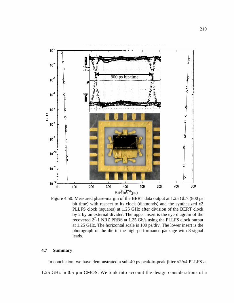
210
4.7 Summary
In conclusion, we have demonstrated a sub-40 ps peak-to-peak jitter x2/x4 PLLFS at
1.25 GHz in 0.5 µm CMOS. We took into account the design considerations of a
Bit time (ps)Figure 4.50: Measured phase-margin of the BERT data output at 1.25 Gb/s (800 ps
bit-time) with respect to its clock (diamonds) and the synthesized x2PLLFS clock (squares) at 1.25 GHz after division of the BERT clockby 2 by an external divider. The upper insert is the eye-diagram of therecovered 27-1 NRZ PRBS at 1.25 Gb/s using the PLLFS clock outputat 1.25 GHz. The horizontal scale is 100 ps/div. The lower insert is thephotograph of the die in the high-performance package with 8-signalleads.
800 ps bit-time

211
broadband PLLFS required in a practical parallel optical data link. The introduction of
jitter by opto-electronic components in a parallel optical data link imposes tighter
constraints on the jitter performance of the PLLFS than a parallel electrical data link
would. The system design considerations force novel design solutions in all components
of the PLLFS. The PLLFS is capable of operation over a wide range from 0.4 to 1.6 GHz
and utilizes a 123 MHz-1.7 GHz VCO, with sub-5 ps rms self-referenced jitter for most of
its high frequency range. The control circuit of the VCO is such that the same frequency of
operation can be obtained by different combinations of current in the cross-coupled (high
jitter) part of the delay cell. This means that over large parts of its operating range, the
PLL described here has the ability to have its output jitter increased, presenting a
convenient mechanism to test the robustness to jitter of a link.
212
Chapter 5
Mux/Demux Array Design
In this chapter, we focus on the N:1 multiplexer and 1:N demultiplexer arrays (shaded
areas in Figure 5.1) required for a parallel data link as shown in the block diagram of the
Opto-Electronic System (OES) that we began with in Chapter 1. We demonstrate two
multiplexer/demultiplexer arrays: the PONIMUX IC whose high-speed link width, M, is
12 and degree of multiplexing, N, is 2 (corresponding to the notation in Figure 5.1), and
the PONI ROPE MUX/DEMUX chipset, where M = 11 and N = 4.
We discussed the design, implementation, and demonstration of the key circuit
components of high-speed flop-flops, multiplexers, receivers, transmitters, low output-
impedance clock buffers, and the low-skew clock distribution circuitry in Chapter 3. The
we discussed the design, implementation, and demonstration of a low-jitter wide-range
selectable x2/x4 PLLFS in Chapter 4. These components are used to arrive at the design
considerations of a broadband N:1 multiplexer and a 1:N demultiplexer in Section 5.1,
which in turn are used to demonstrate a 1:4/4:1 mux/demux BER test circuit in 0.5 µm
CMOS process technology, that achieved 2.80 Gb/s operation at a BER < 10-13 for 231 - 1
NRZ PRBS data patterns, which is discussed in Section 5.4. The results from the 1:4/4:1
demux/mux BER test circuit and the clock distribution technique in Chapter 3 (Section
3.7.8 on page 105) obtain the demonstration of the 12-wide 2.5 Gb/s/channel mux/demux
array IC (PONIMUX IC) that achieves an edge-connection data-bandwidth density of

213
55 Gb/s/cm, which is discussed in Section 5.5. The validation of the above components,
along with the low-jitter wide-range x4 PLLFS discussed in Chapter 4, is key to the
demonstration, in Section 5.6, of an 8.8 W, 11-channel 2.5 Gb/s/channel half-speed 4:1/
1:4 multiplexer/demultiplexer array chipset with an integrated sub-50 ps peak-to-peak
jitter x4 PLLFS at 1.25 GHz, in relatively modest 0.5 µm CMOS process technology. The
integrated x4 PLLFS is capable of operation from 0.4 to 1.6 GHz.
The chipset achieves an edge-connection data-bandwidth density of 50 Gb/s/cm,
which is a factor of 12.7 better than the flex connector interface used to connect the system
board and the IO board in the state-of-the-art HP 785/J7000 Forte workstation.The skew
Electrical IO (LVDS, GTL, GLVDS)
VCSEL Array PIN Diode Array
Sour
ce C
lock
MM
MN
MN MN
Con
trol
Optional Datapath
Tx Bridge
φ F1/
kNφF1
φF1/N
φF1/kN
φF1/kN
clockdata
Figure 5.1: Correspondence of the discussion in this chapter to the OESIC block diagram in Figure 1.10.
1:N demux array Chapter 5
N:1 Mux array Chapter 5
φF1/N
Laser Driver ArrayOE Pre-amplifier Array
Decision Circuit Array
xkN PLLFS
mN
Rx Bridge
Align circuit.

214
of the interface was measured to be better than 25 ps. The introduction of jitter by the
opto-electronic components in a parallel optical data link was determined to dominate the
jitter of the high-speed output interface (2.5 Gb/s/channel) of the chipset in optical
loopback. This jitter contribution needs to be addressed in order to improve the robustness
of parallel optical data links for data rates in excess of 2.5 Gb/s/channel.
5.1 Broadband 1:N Demultiplexer and N:1 Multiplexer
An N:1 multiplexer (also called an N:1 serializer) converts N data streams at data rate
B bits/s to a single data stream at BN bits/s. A 1:N demultiplexer (also called a 1:N
serializer) performs the reverse operation and converts the serial data stream running at
BN bits/s to N data streams running at B bits/s. Note that time is conserved in a system
with an N:1 multiplexer driving a 1:N demultiplexer. When N is a power of 2, the
multiplexing and demultiplexing can be done in a binary fashion, where at every stage the
signal is multiplexed or demultiplexed by a factor of two. The number of stages of
multiplexing or demultiplexing is given by log2N. This offers the fastest method of
multiplexing because the basic unit is a merged mux flip-flop (see for example, Figure
3.29), which combines the mux which has the fastest logic topology, with the storage
element). It also offers the fastest method of demultiplexing because demultiplexing is just
a latching operation based on a continuously running clock signal.
A second option in implementing an N:1 multiplexer is to parallel-load the data in one
cycle into an N-bit shift register and then serially shift the data down the register in N-1
clock cycles [76]. At the demultiplexing end, the serial data is serially stored into a shift
register for N cycles and then moved into an N bit register in parallel at the end of the N
cycles. The disadvantage of this method is that the logic for implementing the functions of
the shifting and parallel loading in the shift register become the limiting factors in the
achievable speed of operation of the multiplexer circuit.

215
The third option is to use a wired-or combinational circuit as shown in Figure 5.2 and
Figure 5.8. The wired-or combinational circuit requires a circuit to generate and align the
N select signals. At the demultiplexing end, a similar circuit is needed to generate and
align the N select signals so that the serial data can be sampled into N parallel flip-flops.
This is a disadvantage, because the output of the receiver running at BN bits/s must drive a
large load corresponding to the input capacitance of the N flip-flops. The wired-or
combinational multiplexer is discussed in more detail in Section 5.1.3 on page 220.
5.1.1 Full-Speed Clocking versus Half-Speed Clocking
Data links with multiplexers and demultiplexers are classified as full-speed clocked or
half-speed clocked data links depending on whether the high-speed clock runs at the same
speed as the data channel(s) or at twice the speed of the data channel(s). In a full-speed
clocked link, the link supports data at bit rate B bits/s and clock at bit rate 2B bits/s (B Hz).
This incurs the costs of distributing a clock running at twice the bit rate to each channel in
a parallel link, generating slower-speed clocks and latching the output data. The advantage
of this approach is that the data is retimed before it is transmitted and after it is received.
Half-speed clocking has a more stringent requirement on the duty cycle of the clock that is
used to generate the select signals at the last stage of multiplexing. A non-50% duty cycle
would mean that every other transmitted bit is smaller than the adjacent bit. In other
words, the non-50% duty cycle of the clock migrates to the data, reducing the phase-
margin at the receive side. In a half-speed link, the power consumed by the clock
distribution circuitry can be reduced by better than a factor of two because of the lower
power consumed by the clock distribution circuitry and reduction in the components of a
TFF and HSDFF from each link. It is to be remembered that the CMOS power-delay curve
is a hyperbolic curve. Alternatively, the data transmission speed can be increased above
that of a full-speed link in the same IC technology. This approach is meaningful in a

216
parallel optical data link if the laser diode turn-on delay induced time jitter is less than
10% of the bit time. The effective input clock-to-data phase-margin at the receiver first-
level demultiplexer is also reduced by the amount of laser diode turn-on delay induced
time jitter (which is magnified by the opto-electronic receiver circuitry).
To summarize, half-speed and full-speed multiplexing/demultiplexing architectures
differ in one main aspect: Presence or absence of a clock running at twice the data rate
which is used to retime the transmit and received data. This has significant consequences
on the power consumption and the maximum data rate that can be achieved in the link. In
the next section, we discuss the architecture of a full-speed N:1 Multiplexer and 1:N
demultiplexer, keeping in mind that the discussion applies to a parallel data link.
5.1.2 N:1 Multiplexer
We discuss the two different multiplexer architectures of a hierarchical 2:1
multiplexer architecture (e.g., [87]) and a single-stage N:1 multiplexer architecture (e.g.,
[43]), from the perspective of operating-frequency range. Figure 5.2 shows the schematic
and symbol of a differential 2:1 selector which is implemented in pseudo-nmos style
wired-or logic, producing complementary output signals.
This selector is used in conjunction with retiming flip-flops as shown in Figure 5.4, so
that the data that is to be sampled is stable, and meets the set-up and hold-time
OUT+ OUT-
D1-D2- D1+
s- s+ s- s+
D2+
D1
D2
2:1 selector OUT+,OUT-
D2+,D2-
s-s+
D1+,D1-M1
M2 M3
M4 M5
M6
M7
M9
M8
M10
Figure 5.2: Schematic and symbol of 2:1 selector using pseudo-nmos style wired-or logic.

217
requirements of the 2:1 selector. In this scheme, D1+ and D1- are available when the clock
is low (i.e., clk+, clk- = 0,1). D2+ and D2- are available and stable when the clock is high
(clk+, clk- = 1,0).
A true differential multiplexer design is used instead of the complementary pseudo-
NMOS wired-or logic style 2:1 selectors shown in Figure 5.2, for high-speed operation.
The schematic of the true differential 2:1 multiplexer is shown in Figure 5.3, which is the
same as the circuit schematic in Figure 3.26, but for the APLSD load devices. This is a
simple modification of the schematic in Figure 5.2 where the transistors M2,M7 and
M3,M8 are combined and form a differential pair. Their respective drains are connected to
differential pairs formed by M4,M9 and M5,M10 respectively. The sources of the “select”
differential pair are returned to ground through a tail current sink. This architecture
operates at a higher data rate than the simple 2:1 selector architecture. The disadvantage of
this topology is that the output voltage swing is close to the positive rail and needs to be
level shifted and buffered to drive the output Tx circuit. This incurs a power consumption
penalty for the increase in operating speed.
This circuit has input-data dependent distortion at the outputs (which is independent of
the load devices) due to the coupling of the parasitic device-channel capacitance and the
M2,7 M3,8
M4 M9 M5 M10
M1 M6
D1- D1+ D2- D2+
s- s+
bias
Figure 5.3: Schematic of differential 2:1 multiplexer
OUT-OUT+

218
parasitic capacitance at the source of the upper differential pair that is not selected to the
output node. For example, if s- corresponds to logic 0, M2,7 is off and M3,8 is on. The
output is then controlled by the inputs D2+ and D2- through M5 and M10. During this
time, D1+ (D1-) may be on (off) or off (on). This causes variations in the trout- (tfout-), the
rise (fall) time of OUT- and tfout+ (trout+), the fall (rise) time of OUT+ respectively. When
D1+ is on and D1- is off, M10 sees the channel capacitance of M9 and the parasitic
capacitance at the source of M4 and M9, which increases the rise- or fall-time of OUT-,
while M5 does not see this extra capacitance. When D1+ is off and D1- is on, M5 sees the
channel capacitance and the parasitic capacitance associated with the source of M4 and
M9. This increases the rise or fall time of OUT+ as the case may be. This input data-
dependent output loading becomes more significant at higher operating frequencies
because the rise- or fall-time of a voltage signal across a capacitor is proportional to the
amount of current available to charge the capacitor. This can be rectified in principle by
adding a limiting amplifier after the level-shift circuit following the multiplexer. This
requires additional power consumption and delays the output of the muxed data, requiring
the delay on the clock output line to be matched to the extra delay on the data line. This
design can be merged with the master latch of a flip-flop to form a merged mux flip-flop
(see for example, Figure 3.29) for the fastest operating speed.
The slow-speed input DFFs (Figure 3.37, Figure 3.38) in Figure 5.4 are differential
output dynamic flip-flops. Figure 5.4 shows the schematic and symbol of the 2:1 mux
which uses the 2:1 selector in Figure 5.2. This circuit choice of dynamic flip-flops is
useful for low-power, low-frequency operation, when the power-supply and substrate
noise generated by the full-rail clock distribution circuitry is not a major concern from
packaging and mixed-signal design considerations. Figure 5.5 shows the schematic and
symbol of the high speed 2:1 mux. In this case, high speed DFFs (HSDFFs) are used
instead of the DFFs as in Figure 5.4. The latch in Figure 5.5 is a high-speed latch which is

219
the master latch of the HSDFF. The 2:1 selector in Figure 5.5 is a resized version of the
selector in Figure 5.2.
Figure 5.6 shows the schematic of the 4:1 multiplexer that uses the components
discussed above. The retiming latches used in the 2:1 muxes ensure that the data meet the
setup- and hold-time requirements of the 2:1 selector and reduces the impact of reverse
clocking in the multiplexer architecture. The input data D1 through D4 are held stable by
signal c1- in Figure 5.6, so that the data are stable half a clock-period before they are
actually used by the 2:1 muxes. The data outputs of the HSMUX are latched into the
HSDFF by a delayed version of the input clock. The delaying is achieved by a cascade of
three inverters. The fundamental problem with delay circuits is that the relationship
between the clock and data cannot be maintained over a large temperature and frequency
Figure 5.4: Schematic and symbol of 2:1 mux composed of dynamic flip-flops.
2:1
MUX
+ -
q1
q2
OUT+,OUT-
clk+ clk-
D-FF
D-FF latch
clk+
D1
D2
2:1 selector
clk-
clk+
OUT+,OUT-
D1+,D1-
D2+,D2-
q1
q2
s-s+
HSDFF+-
D1
D2
2:1 selector
+s-
s
OUT+,OUT-
D1+,D1-
D2+,D2-
HSDFF+-
+-
q1+,q1-
q2+,q2-
clk-
clk+
2:1
MUX
+ -
HS
q1+,q1-
q2+,q2-
OUT+,OUT-
Figure 5.5: Schematic and symbol of high-speed 2:1 mux composed of HSDFFs (Figure 3.12).
clk+ clk-
latch

220
range. Circuit solutions like a DLL have significant area, power and complexity
overheads. The positioning of the latching clock-edge with respect to the input data over
the desired frequency and temperature range is such that the performance at the lower-end
of the operating range is preferred. In other words, if the positioning of the clock edge was
such that latching at higher frequencies would result in a case where the data may not be
latched at lower frequencies, it was not preferred. This design choice was favored because
the largest operating range of frequencies is preferable for parallel link operation.
5.1.3 Wired-OR Tree Multiplexer
Figure 5.7 shows the overall schematic of the single-stage multiplexer architecture.
TXOUT+ and TXOUT- are the high-speed outputs which are terminated to VTT through
50 Ω. Signals c1+ and c1d+ in Figure 5.7 in differ in phase by one-half the period of the
master clock. This architecture requires the generation of two differential clock signals (in
order to reduce the impact of process variations on clock delay circuitry). Signal c1d- in
Figure 5.7 is one-fourth the frequency of the master clock, but is one-half of the master
clock period behind signal c1-. c1- is used to latch the inputs to the multiplexer and
Figure 5.6: Schematic of full-speed 4:1 multiplexer composed of 2:1 muxes.
D1
D3
D0
D2
2:1MUX
+ -
2:1MUX
+ -
2:1
MUX+ -
TFF-
HS
RESET
clk+
clk-
c1+
c1-
HSDFF+-
T/X
TFF-
++
c0- c0+
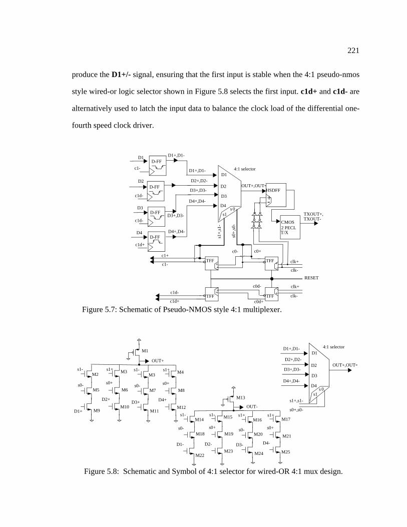
221
produce the D1+/- signal, ensuring that the first input is stable when the 4:1 pseudo-nmos
style wired-or logic selector shown in Figure 5.8 selects the first input. c1d+ and c1d- are
alternatively used to latch the input data to balance the clock load of the differential one-
fourth speed clock driver.
D1
D2
4:1 selector
0s1
s
OUT+,OUT-D2+,D2-
D3+,D3-
D4+,D4-D3
D4
D1+,D1-
s1+,
s1-
s0+,
s0-
D-FF
D3+,D3-D-FF
D4+,D4-D-FF
D1+,D1-D-FF
TFF-
RESET
clk+
clk-
c1+
c1-
HSDFF
+-
CMOS2 PECLT/X
TFF-
++
c0- c0+
TFF-
clk-
clk+
c1d+
c1d- TFF
-++
c0d-
c0d+
c1-
c1d-
c1d-
c1d+
D1
D2
D3
D4
Figure 5.7: Schematic of Pseudo-NMOS style 4:1 multiplexer.
TXOUT+,TXOUT-
OUT+
s1- s1+
s0+
M1
M2
M5
M3
M6
OUT-
s0-
s1- s1-
s0+
M13
M14
M18
M15
M19
D1+
D2+
D1- D2-
M10M9
s0-
M23M22
D1
D2
4:1 selector
0s1
s
OUT+,OUT-D2+,D2-
D3+,D3-
D4+,D4-D3
D4
D1+,D1-
s1+,s1-
s0+,s0-
s1- s1+
s0+
M3
M7
M4
M8
D3+ D4+
M12M11
s0-
s1+ s1+
s0+
M16
M20
M17
M21
D3- D4-
M25M24
s0-
Figure 5.8: Schematic and Symbol of 4:1 selector for wired-OR 4:1 mux design.

222
The architecture shown in Figure 5.7 has a reduced operating frequency and junction
temperature range as compared to the architecture shown in Figure 5.6. As the operating
frequency of the full-speed clock falls, or as the junction temperature is reduced from the
design values, the clock waveform has smaller rise and fall times.This coupled with the
increased drive of the 4:1 selector results in a reduction of the input clock-to-data phase-
margin of the HSDFF which latches the output of the 4:1 selector in Figure 5.7. This is
due to the inability of the full-speed clock or a delayed version thereof, to maintain the
relationship of the latching-clock edges to data over the desired frequency and junction
temperature ranges. Additionally, the delay of the output of the TFF to the input clock
waveform becomes more significant as the clock frequency and junction temperature
increases. This affects the timing relationship of the half-speed, fourth-speed clocks and
the complimentary data latched by the fourth-speed clocks. This affects the setup- and
hold-time of the data at the 4:1 selector inputs. The use of a 4:1 selector which uses both
the half-speed and fourth-speed clock waveforms, which are not phase-aligned, makes the
architecture more vulnerable to process variations, impacting their performance. The
effective operating frequency range of this architecture was found to be less than 200
MHz over a temperature range of 20 °C. This architecture pays a higher price in power
dissipation because of the need for the generation of two fourth-speed clocks. This is to
avoid the need for delay elements which reduce the operating range, due to the
fundamental uncertainty of these delay elements due to process and junction temperature
variations. The use of a DLL to phase-align the half-speed and fourth-speed clock signals
is a better solution, but has significantly more area, power and complexity costs.

223
5.1.4 1:N Demultiplexer
We discuss the components of the demultiplexer prior to the architecture of the
demultiplexer. The input differential signals are latched by a high-speed differential flip-
flop whose schematic and symbol are shown in Figure 3.12. This data are routed to the
demultiplexer whose block diagram is shown in Figure 5.9, which is a topology that finds
application in Si BJT [87][85] and GaAs MESFET technologies. An alternate topology
that has been used to implement a demultiplexer in CMOS technology is reported in [86].
The components of the demultiplexer are HSDFFs (Figure 3.12), TFFs (Figure 3.36), and
DFFs (Figure 3.37 and Figure 3.38), which have already been discussed. CLK+ and CLK-
are the differential clock signals that are distributed on the IC. Signals c0+ and c0- are the
half-speed clocks signals produced by the first TFF. The DFFs have single-ended outputs.
Signals c1+ and c1- are the differential one-fourth-speed clock signals. Data is latched into
the HSDFF at the falling edge of CLK-. Figure 5.10 schematically shows the simulation of
the demultiplexer in Figure 5.9.
DFF
DFF
latch
DFF
latch
out4
out2
out3
out1
q11+
q12+q12t+
q22t+
q24t+
+
c0+c0-
c1
c1-
RESET
CLK-
Data+, Data-qin+
TFF+-
+- TFF
-CLK+
Figure 5.9: Schematic of the full-speed 1:4 demultiplexer.
+
DFF
DFF
latch
HSDFF+-
DFF

224
The waveforms at the nodes in Figure 5.9 are shown schematically in Figure 5.10.
qin+ is the output of the HSDFF. The components of the serial data stream to be
demultiplexed are indicated by 1, 2, 3 and 4 in Figure 5.10. Since CLK- drives the positive
CLK input of the TFF in Figure 5.9, c0+ and c0- are triggered off the falling (rising) edge
of CLK- (CLK+). DFFs are used at data rates less than 500 Mb/s. Care is taken to balance
the clock loads of the TFFs so that the differential nature of the clock signals is preserved.
The strategy of the demultiplexer is to group data values 1 and 3 at q12t+, and values 2
and 4 at q11+, so that q11+ and q12+ have overlapping data values 1 and 2 in time, as
shown in Figure 5.10. A similar strategy is pursued in the succeeding stage with the use of
the c1+ and c1- clocks to generate the final demultiplexed outputs. The demultiplexer
requires only single-ended signals after the high-speed flip-flop (HSDFF) stage. This
facilitates the use of TSPC style DFFs which result in lower power consumption as
compared to the differential high-speed latches (HSDFF).
clk-qin+c0+c0 -
q12t+q11+q12+
c1+c1-
q22t+q24t+out3out2out1out0
1 2 3 4
1 3 2 4 1 3
21
4
21
3
Figure 5.10: Schematic of waveforms at the various nodes in Figure 5.9.
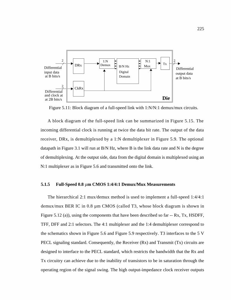
225
A block diagram of the full-speed link can be summarized in Figure 5.15. The
incoming differential clock is running at twice the data bit rate. The output of the data
receiver, DRx, is demultiplexed by a 1:N demultiplexer in Figure 5.9. The optional
datapath in Figure 3.1 will run at B/N Hz, where B is the link data rate and N is the degree
of demultiplexing. At the output side, data from the digital domain is multiplexed using an
N:1 multiplexer as in Figure 5.6 and transmitted onto the link.
5.1.5 Full-Speed 0.8 µm CMOS 1:4/4:1 Demux/Mux Measurements
The hierarchical 2:1 mux/demux method is used to implement a full-speed 1:4/4:1
demux/mux BER IC in 0.8 µm CMOS (called T3, whose block diagram is shown in
Figure 5.12 (a)), using the components that have been described so far -- Rx, Tx, HSDFF,
TFF, DFF and 2:1 selectors. The 4:1 multiplexer and the 1:4 demultiplexer correspond to
the schematics shown in Figure 5.6 and Figure 5.9 respectively. T3 interfaces to the 5 V
PECL signaling standard. Consequently, the Receiver (Rx) and Transmit (Tx) circuits are
designed to interface to the PECL standard, which restricts the bandwidth that the Rx and
Tx circuitry can achieve due to the inability of transistors to be in saturation through the
operating region of the signal swing. The high output-impedance clock receiver outputs
DRx
CkRx
1:NDemux B/N Hz
Digital
N:1Mux
Tx
Die
Differential
output data
2
2
2
Differential
Figure 5.11: Block diagram of a full-speed link with 1:N/N:1 demux/mux circuits.
Domaininput dataat B bits/s at B bits/s
and clock atDifferential
at 2B bits/s

226
directly drives the flip-flops, whose schematic is shown in Figure 3.12, without the use of
the APLSD load devices.
The reset signal in Figure 5.12 (a) resets the TFFs in both the demultiplexer and the
multiplexer. The demultiplexer and the multiplexer are separately clocked to simulate
clocking conditions on the actual parallel link interface IC. This also simplifies the full-
speed clock distribution problem on the IC. din+/- and sout+/- in Figure 5.12 (a) are the
serial data stream from the BERT and the serialized output of the 1:4/4:1 BER circuit
respectively. This data stream is fed back into the BERT for the BER measurement.
Figure 5.12 (b) shows the measured error-free 1:4/4:1 BER circuit output (sout+/- in
Figure 5.12 (a)) eye-diagram corresponding to a BER < 10-13 for 231 - 1 NRZ PRBS,
which has a measured eye-width of 704 ps and an eye-height of 540 mV. The BER
increases to better than 10-11 for a data rate of 990 Mb/s. The lower traces in Figure 5.12
(b) are the divide-by-four clocks (d_div/4 and s_div/4 in Figure 5.12 (a)) produced by the
demultiplexer and the multiplexer respectively, which are measured at 249 MHz. All
waveforms are attenuated by 20 dB prior to display on the oscilloscope. There were no
frx frx frx
tx
tx tx
Demultiplexer1:4
sclk
+/-
din+
/-
dclk
+/-
d_di
v/4
s_di
v/4
rese
t
sout
+/-
rese
t
Multiplexer4:1
(a)(b)
50 m
V/d
iv
Figure 5.12: (a) Block diagram of 1:4/4:1 mux/demux BER circuit in 0.8 µm CMOS and (b) 980 Mb/s eye-diagram. The horizontal scale is 1 ns/div and the vertical scale is 50 mV/div.

227
errors for frequencies down to 400 MHz, below which the BER circuit was not tested. The
high-frequency performance of the BER circuit is constrained by the design choice of the
positioning of the latching clock in Figure 5.6 such that the operation of latching the data
at higher frequencies does not result in latching errors at lower frequencies. At high
frequencies, circuit delays can easily add up to a significant fraction of the clock period,
requiring a different clock edge to latch the data than at lower frequencies, where the
circuit delay would be less than half-a-clock period.
5.2 Half-Speed 4:1/1:4 Mux/Demux Circuitry
A half-speed 4:1 multiplexer can be obtained from a full-speed 4:1 multiplexer by
removing the output retiming flip-flop HSDFF in Figure 5.6. The schematic of a half-
speed 4:1 multiplexer so obtained is shown in Figure 5.13. The half-speed 1:4
demultiplexer shown in Figure 5.14, is the same as the full-speed 1:4 demultiplexer
schematic in Figure 5.9 without the input retiming HSDFF.
A block diagram description of the concept of a half-speed link can be summarized in
Figure 5.15. The incoming differential data and clock are running at the same bit rate. The
Figure 5.13: Schematic of half-speed 4:1 multiplexer composed of 2:1 muxes.
D1
D3
D0
D2
2:1MUX
+ -
2:1MUX
+ -
2:1
MUX+ -
HS
RESET
clk+
clk-
c1+
c1-
TX
TFF-+
c0- c0+

228
output of the data receiver DRx is demultiplexed by clocking the data into flip-flops FF1
and FF2 on opposite phases of the received differential clocks.
This creates two data streams on the IC which are 180° out of phase, which can be
brought into phase alignment by delaying the earlier data by a latch. The output of the 1:2
demultiplexer that has been effected by the first level of flip-flops can then be
demultiplexed using two 1:4 demultiplexers (see for example, Figure 5.9) described in the
last section as shown in Figure 5.15. This creates a byte running at one-fourth the link
clock rate as opposed to a nibble at one-fourth the link clock rate for the full-speed data
link strategy described earlier. This approach can be modified to generate a nibble running
DFF
DFF
DFF
out4
out2
out3
out1
q11+
q12+q12t+
q22t+
q24t+
+
c0+c0-
c1
c1-
RESET
CLK-
Data+, Data-
TFF+-
CLK+
Figure 5.14: Schematic of half-speed 1:4 demultiplexer.
DFF
DFF
DFF
latch
latch
latch
DRx
CkRx
FF1
FF2
1:NDemux
1:NDemux
B/N Hz
Digital
N:1Mux
N:1Mux
2:1Mux
Tx
IC
Differential
output data
2
2
2
Differential
Figure 5.15: Block diagram of a half-speed link with 1:N/N;1 demux/mux circuits.
Domaininput data
at B bits/sat B bits/s
1:2 demux
and clock at

229
at half the link-clock rate which would mean that the optional datapath in Figure 3.1 will
run at B/2N as opposed to B/N, where N is the degree of demultiplexing. Therefore, the
half-speed clocking strategy for a parallel data link can be used to double the data rate or
reduce the power consumption for the same data rate as in a full-speed clocked link.
Doubling the link data rate forces the design choice of doubling the width of the datapath
or increasing the frequency of operation of the datapath. This choice depends on the
technology, the logic style under consideration, and the data rates under consideration.
5.3 PECL Half-Speed 1:4/4:1 Demux/Mux Circuit in 0.8 µm CMOS
An IC incorporating a BER circuit to provide proof of concept was shipped in the 0.8
µm CMOS process as IC T4. The die size of T4 is 2.2 mm x 1.85 mm. The schematic of
the BER circuit is shown in Figure 5.16 for a DC-coupled interface. The parasitics
associated with the bond-wires and bond-pads are shown in the schematic as well.
3.0 V
3.0V
3.0 V
Cpad
Cpad
Cpad
ClockRx
FF
FF
TX BUF LS
MUX
Differential PECL Output
Switching 5.0 mA in 0.5 ns
5.0 mA DC, switching 5.0mA in 250 ps41 mA DC
switching 12 mA
12.0 mA DCswitching 4.0 mA in 0.5 ns
10.0 mA DCSwitching 10.0 mAin 250 ps
44 mA DCSwitching
6 mA in 25 0ps
1 m SMA cables
Differential PECL Inputs
2:1
Figure 5.16: 0.8 µm CMOS BER circuit (T4) schematic.
Rx
50 Ω

230
Simulations accounted for the package interconnect. Current consumption of the various
components at 5 V is shown as well. T4 interfaces to the 5 V PECL signaling standard.
Consequently, the Receiver (Rx) and Transmit (Tx) circuits are designed to interface to
the PECL standard, which restricts the bandwidth that the Rx and Tx circuitry can achieve
due to the inability of transistors to be in saturation through the operating region of the
signal swing. The high output-impedance clock receiver outputs directly drives the flip-
flops (“FF” in Figure 5.16) whose schematic is shown in Figure 3.12, without the use of
the APLSD load devices. The 2:1 multiplexer is composed of a true differential 2:1 MUX
(Figure 3.26 without the APLSD load devices) followed by a level-shift (“LS” in Figure
5.16) and a buffer (“BUF” in Figure 5.16) to drive the Tx circuit (Figure 3.50) which
injects the data as a PECL signal onto the link. The PECL signaling standard, the high
output-impedance clock drivers and the non-use of the APLSD load devices increase the
power consumption and limit the maximum speed that the half-speed BER circuit can
achieve.
5.3.1 Measurements of PECL Half-speed 4:1/1:4 Demux/Mux IC
Half-speed testing requires that the data and the clock arriving from the BERT be at
the same bit rate. Half-speed clocks may not be available from BERTs, which typically
provide full-speed clocks. A solution is to use an external divider to divide the full-speed
BERT clock output by 2. An MC100EL32 [95], manufactured in Motorolla’s MOSAIC
III Si BJT process technology, is used as the external ECL divider. The device has a
typical bandwidth of 2.2 GHz, with decreasing output amplitude beyond input frequencies
of 2.2 GHz. The divider is mounted on a ceramic substrate which is fixtured in an
enclosed brass RF test fixture with SMA connectors. The test-fixture interconnect has a -3
db bandwidth greater than 12 GHz. Measured waveforms of the divider output indicate

231
operating frequency dependent output-distortion and attenuation of output voltage to 600
mV at an input frequency of 3.0 GHz.
Figure 5.17 shows the differential output of the external divider output at (a) 0.5 GHz
and (b) 1.0 GHz, corresponding to input frequencies of 1.0 GHz and 2.0 GHz respectively.
The positive output has an amplitude of 800mV and the negative output has an amplitude
of 728 mV at 0.5 GHz (Figure 5.17 (a)) output frequency. At 1.0 GHz output frequency,
the positive output has an amplitude of 800 mV and the negative output has an amplitude
of 744 mV (Figure 5.17 (b)). A second divider part was mounted on a copper-clad General
Purpose Board (GPB) with SMA connectors soldered directly onto the packaged divider
pins. This did not modify the performance of the divider from the waveforms shown in
Figure 5.17. This forces the conclusion that the distortion on the divider output is intrinsic
to the part. The cause of the Amplitude Modulation (AM) of the divider output, whose
period is approximately twice that of the divider output waveform, is unknown.
Figure 5.18 shows the measured eye-diagram at (a) 1.5 Gb/s and (b) 1.8 Gb/s
corresponding to 231 - 1 NRZ PRBS input data patterns. All waveforms are attenuated by
20 dB prior to display on the scope. Both waveforms are on the same vertical scale of
20 mV/division. The eye-diagram at 1.5 Gb/s corresponds to BER < 10-13 and eye-width
of 418 ps. At 1.8 Gb/s, the BER test circuit is at the limit of its performance. Significant
(a) (b)
200
mV
/div
200
mV
/div
Figure 5.17: External divider output at (a) 0.5 GHz and (b) 1.0 GHz. The hori-zontal scale is 500 ps/div for both (a) and (b).

232
ISI-effects and non-uniform eyes can be observed in Figure 5.18 (b). This effect is most
probably due to clock duty-cycle distortion originating from the external divider output. A
BER < 10-13 was obtained only with 223 -1 NRZ PRBS input data patterns while 231 -1
NRZ PRBS input data patterns resulted in a measured BER < 10-11. The eye-width in both
cases was 294 ps out of maximum possible 556 ps. Performance at 1.8 Gb/s also required
that the differential flip-flop power supply be raised above the analog power supply
(receivers and transmitters) by 0.5 V, pointing to differential clock common-mode voltage
problems. This could be most likely due to differential waveform distortion by inverter
buffers due to process variations. The differential eye closure is also likely to be occurring
to a lesser extent by the input data-dependent output-distortion of the 2:1 multiplexer in
Figure 5.3.
(a) (b)
20 m
V/d
iv
20 m
V/d
iv
Figure 5.18: Eye-diagrams of 1:2/2:1 demux/mux BER circuit on T4 at (a) 1.5 Gb/s and (b) 1.8 Gb/s. The horizontal scale is 200 ps/div for both (a) and (b).

233
5.4 LVDS 4:1/1:4 Mux/Demux
The flip-flops designed for the prescalers (Figure 3.20) are used in conjunction with
the low output-impedance clock buffers (Figure 3.46), electrical LVDS receivers (Figure
3.49) and transmitters (Figure 3.53), to design a half-speed 1:4 Demux (Figure 5.14) 4:1
Mux (Figure 5.13) BER circuit with an LVDS interface, running at 2.8 Gb/s. The IC
(called T9), implemented in 0.5 µm CMOS, measures 2.4 mm x 1.67 mm. The die
photograph of the IC is shown in Figure 5.20. We migrate to the LVDS standard because
the link signaling levels enable the design of high-speed low-power receiver and
transmitter circuits, unlike the PECL signaling levels. The schematic and test set-up of the
IC (T9) is shown in Figure 5.19. The IC takes half-speed data and a half-speed clock (from
an external divide-by-2 circuit as discussed Section 5.3.1 on page 230) inputs. The shaded
box outlines the boundary of the IC. The electrical receive (Rx) and transmit (Tx) circuits,
which are designed for the LVDS signaling standard, are capable of sustaining a data rate
of 3.3 Gb/s/channel. Figure 5.19 also shows the power consumption of the various blocks.
This power consumption is much higher than what it can be, because of the use of
RxTx
1.75V
1.75v
1.75V
36 mW
27.8mW
Rx + Bufs
1.75V
1/2Tx
27.8mW
1.75v
Data out
Clock out
Data input
Half-speed
clock input
1:4 4:1
354 mW
270mW
191mW
210mW
Data = 464.8 mWClock =651.8 mW
Figure 5.19: Schematic and test-setup of IC (T9) shown in Figure 5.20.

234
prescaler D flip-flops (Section 3.4 on page 64) in the demux/mux circuit which consumes
more power and has a higher clock-load. The power consumption of the circuits that are in
the datapath is 465 mW, while the clock distribution circuitry consumes 652 mW from a
3.6 V supply. An optimized 12-wide 2.5 Gb/s/channel half-speed electrical interface (see
Section 5.5 on page 237) has an amortized power dissipation of 185 mW/channel.
5.4.1 Half-speed 1:4/4:1 Demux/Mux IC Measurements
The measured results of T9 indicate that the 4:1/1:4 Demux/mux circuit is capable of
robust operation at 2.8 Gb/s. Further increase in operating speed seems to be hampered by
packaging issues. The clock buffer power connection has a long bond wire, which needs
to be shortened to see if higher speed operation is possible. Figure 5.21 (a) shows the
measured eye-diagram and (b) shows the BERT referenced jitter histogram of the data.
The rms jitter of 11.10 ps indicates that the circuit introduces low jitter. The eye-diagram
at 2.8 Gb/s (ideal bit time of 357 ps) has a measured eye-width of 284 ps and an eye-height
Die photograph of testdie (T9) to test 4:1/1:4 Mux/Demux. The testdie has an area of 2.4 mm x 1.67 mm in 0.5 µm CMOS. IC imple-ments BER circuit.
Figure 5.20: Testdie (T9) photograph. IC measures 2.4 mm x 1.67 mm.
1:4/4:1 Demux/Mux
Buf
fer
Dat
a R
x
Clk
Rx
ClockBuffers 1/2
DataTx
ClkTx
1/2Clock
Buffers

235
of 300 mV. The input data window for error-free operation is 278 ps. The eye-diagram
and measurements correspond to BER < 10-13 for 231-1 NRZ PRBS.
5.4.2 Data to Clock and Clock to Data Coupling
Figure 5.21: (a) Error-free 2.8 Gb/s eye-diagram and (b) BERT trigger referenced jitter histogram.
(a) (b)
50 ps/div
20 m
V/d
iv
10 m
V/d
iv
100 ps/div
dout+
clk+
clk-
strong data toclock and clockto data coupling.
Figure 5.22: Bondwire coupling induced eye degradation. The horizontal scale is 100 ps/div and the vertical scale is 20 mV/div.
20 m
V/d
iv
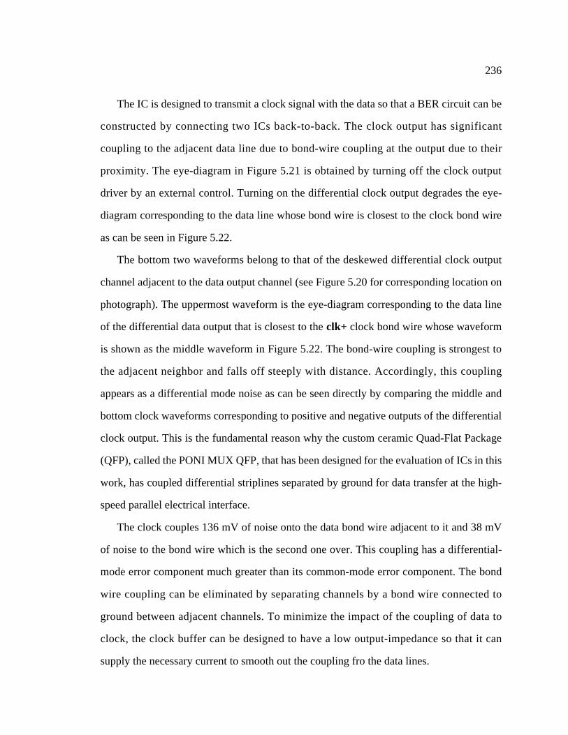
236
The IC is designed to transmit a clock signal with the data so that a BER circuit can be
constructed by connecting two ICs back-to-back. The clock output has significant
coupling to the adjacent data line due to bond-wire coupling at the output due to their
proximity. The eye-diagram in Figure 5.21 is obtained by turning off the clock output
driver by an external control. Turning on the differential clock output degrades the eye-
diagram corresponding to the data line whose bond wire is closest to the clock bond wire
as can be seen in Figure 5.22.
The bottom two waveforms belong to that of the deskewed differential clock output
channel adjacent to the data output channel (see Figure 5.20 for corresponding location on
photograph). The uppermost waveform is the eye-diagram corresponding to the data line
of the differential data output that is closest to the clk+ clock bond wire whose waveform
is shown as the middle waveform in Figure 5.22. The bond-wire coupling is strongest to
the adjacent neighbor and falls off steeply with distance. Accordingly, this coupling
appears as a differential mode noise as can be seen directly by comparing the middle and
bottom clock waveforms corresponding to positive and negative outputs of the differential
clock output. This is the fundamental reason why the custom ceramic Quad-Flat Package
(QFP), called the PONI MUX QFP, that has been designed for the evaluation of ICs in this
work, has coupled differential striplines separated by ground for data transfer at the high-
speed parallel electrical interface.
The clock couples 136 mV of noise onto the data bond wire adjacent to it and 38 mV
of noise to the bond wire which is the second one over. This coupling has a differential-
mode error component much greater than its common-mode error component. The bond
wire coupling can be eliminated by separating channels by a bond wire connected to
ground between adjacent channels. To minimize the impact of the coupling of data to
clock, the clock buffer can be designed to have a low output-impedance so that it can
supply the necessary current to smooth out the coupling fro the data lines.

237
5.5 2.5 Gb/s Twelve Channel 2:1/1:2 Mux/Demux Array IC
We use the components discussed so far: namely, flip-flops (Figure 3.12), dividers
(using the merged mux-flip-flop in Figure 3.29), clock driver circuitry (Figure 3.46), delay
elements (based on the PLLFS VCO delay cells in Figure 4.7), clock selection circuitry
(Figure 3.48), LVDS electrical receive (Figure 3.49) and transmit circuitry (Figure 3.53),
to implement a 12-channel parallel electrical transceiver IC (called the PONIMUX IC) to
provide a bridge between CMOS circuitry and the signaling capabilities of VCSEL-based
parallel optical interconnect technology over a small form-factor 12-wide fiber-optic
ribbon. The IC has a standard LVDS electrical interface with equal data and clocking rates
Figure 5.23: Block diagram of 2:1/1:2 mux/demux circuit with clock distributioncircuit.
selin
1 0
f1
f1
f1
2:1 1:2
Rx
IO +
retim
ing
Tx
I/0
+ re
timin
g
f1/2
Inte
rfac
e B
oard
Inte
rfac
e B
oard
vnp, vnn
vnpout, vnnout
01
0/π phaseselect
0/π°phaseselect
01
clk2
(ful
l-sp
eed) clock2out
(half-speed)
11
diff.lines
1
22
diff.lines
22
diff.lines
CLK PATH Tx Rx°
0/π phase select
insel
1 diff.line
diff.line
clk2 rcvr
1/21/2
Delay
1 0

238
(i.e., half-speed clocking). It has 10 data channels, each implementing a 2:1/1:2 mux/
demux function, 1 clock channel and 1 frame channel. It is designed to be compatible with
the HIPPI-6400 [16] signaling standard, which has an aggregate data-throughput of 8 Gb/
s. The PONIMUX IC enables the insertion of parallel optical interconnect modules into
high-performance computer systems.
The functional block diagram of the PONIMUX IC is shown in Figure 5.23. The
figure schematically separates the IC into two halves -- the Tx portion (left-hand side of
Figure 5.23) and the Rx portion (right-hand side of Figure 5.23). The shaded block titled
Interface Board refers to the evaluation PCB, which interfaces to an LVDS compliant data
source and an LVDS compliant data sink. Though the interface board has been
schematically represented as two blocks in Figure 5.23, it represents one and the same
evaluation board. The shaded area titled “CLK PATH” in the Tx part of the IC receives a
full-speed clock (Clock2 in HIPPI-6400 terminology, and clk2 in Figure 5.23) running at
twice the slow-speed input data rate. This clock can be delayed to latch all the input data
channels successfully. An additional delay-chain is provided for the high-speed clock
output path so that the high-speed input side clock-to-data setup time (the hold time is zero
for the high-speed input flip-flops) can be satisfied across all the channels. Ideally, this
delay chain is located on the Rx side of the IC so that in application, the physical
separation of Tx and Rx ICs will not interfere with clock-to-data setup time adjustment on
the high-speed inputs. The clock selection circuitry to select between different clocks is
implemented using the low-jitter clock-selection circuit architecture in Figure 3.47.
Clock2 (called “clk2” in Figure 5.23) is at the same speed as the data lines in the
context of a HIPPI-6400 data transmission protocol. For the purposes of the functionality
of this IC, a times-2 PLLFS is assumed to multiply the incoming Clock2 signal by a factor
of two before being sent to the Tx part of the PONIMUX IC in Figure 5.23. It is to be
noted that the absence of an internal PLLFS makes the PONIMUX IC an essentially

239
broadband wire-replacement IC, which reduces interconnect form-factor. The CLK PATH
shown in Figure 5.23 also features a 0°/180° phase-select circuit in the clock input and
output paths, in addition to the input and output delay-chains, for additional flexibility in
meeting the clock-to-data setup times at the slow-speed and the high-speed input sides
across a large range of data rates (62.5 Mb/s to 1.25 Gb/s input data rates). The divider in
the CLK PATH section of the IC is not relevant to the functionality of the PONIMUX IC.
The HIPPI-6400 data transmission protocol specifies Clock2 as a signal running
continuously with no specified phase relationship with the data. Accordingly, no delay
chain is provided on the Clock2 output signal (“clk2out” in Figure 5.23) on the slow-speed
output in the Rx portion of the IC. A low-jitter 0°/180° phase-select circuit is implemented
in the slow-speed Clock2 output path to take care of any unforeseen eventuality.
5.5.1 PONIMUX IC Layout and Packaging
Figure 5.24 shows the die photograph of the 0.5 µm CMOS PONIMUX IC. The IC
measures 10.3 mm x 2.3 mm. The IC dissipates 3.74 W in the clocking circuitry and the
2:1/1:2 mux/demux core, 0.72 W for the 2.5 Gb/s high-speed IO, and 1.24 W for the 23
slow-speed 1.25 Gb/s differential receivers and transmitters, for a total of 5.7 W from a
Figure 5.24: Microphotograph of the 0.5 µm CMOS PONIMUX IC. The submittedIC layout was 10.1 mm x 1.8 mm. The die size of the IC is 10.3 mm x2.3 mm.
46=2*(16+4+1+1+1) 46=2*(16+4+1+1+1)
24 2410.3 mm 2.
3 m
m0.72 W 2.5
3.74 W Core
1.24 W 1.25 Gb/s IO
Gb/s IO
MUXRx
MUXTx

240
3.6 V power supply. The total power consumption is expected to be better than 2.9 W in
0.25 µm CMOS from a 2.5 V power supply. The IC layout was guided by the dataflow
requirements of a HIPPI-6400 data transmission source and sink, the need to connect to a
12-wide interface at the high-speed port, and the need to electrically test the IC prior to
integration of the IC with the Agilent PONI Tx and Rx parallel optical link modules [216].
The cavity size of the PONIMUX QFP and the IO requirements of a HIPPI-6400
interface, mandated a tight bond pad pitch (100 µm center-to-center) on the slow-speed
input side of the IC.
The small size of the IC in relation to the package cavity dimension of 11 mm x 8 mm
required an insert to bridge the cavity bonding shelf to the slow-speed side inputs of the IC
in the electrical test-fixture, while maintaining controlled (50 Ω) impedance
characteristics and low-crosstalk. For the purpose of the initial testing, a 10 mil thick
ceramic insert (10.5 mm x 4 mm, with the longest trace length being 7 mm) with 30 µm
(a) (b)Figure 5.25: (a) Photograph of the PONIMUX IC in the PONI MUX QFP cavity.
The QFP is 1.35 inches on a side and has 244 leads on a 20 milpitch. (b) Blow-up of cavity detail showing IC and the insert whichcarries the signals from the slow-speed bonding pads on the IC tothe PONI MUX QFP cavity signal shelf.

241
wide gold traces with edge-to-edge line spacing of 70 µm was used. Electrical
measurements of a packaged ceramic “through” insert indicated a measured impedance of
74 ohms, (calculated odd-mode impedance of 53 ohms), crosstalk of -20 dB and -3 dB
bandwidth of 700 MHz for a 7 mm long trace including 20” of 3M RG178 Shielded
Controlled Impedance (SCI) cable and FR4 PCB traces). Figure 5.25 (a) shows the
PONIMUX IC in the QFP cavity and (b) shows the magnified view of the IC in the QFP
cavity. The insert connects the slow-speed signals to the cavity signal shelf.
5.5.2 PONIMUX IC Test Results
The PONIMUX IC mounted in the PONI MUX QFP (Figure 5.25) is mechanically
fixtured on to the PONIMUX IC evaluation board. Signals are delivered to the board using
3M SCI 50 Ω cables. The loss in these RG178 cables1 dictated that the length of signal
transmission be limited to as short a length as possible (10” was chosen).
1. A 2 foot section of the cable has a measured -3 dB bandwidth of 2.60 GHz. Thefrequency response is down -1.43 dB at 1.25 GHz for the same cable.
a. Reported range is for a DC-coupled interfaceb. Reported range is for a DC-coupled interface
Name Description Value Current Rating
P1 Output Power Not Used N/A
P2 Analog Power (voltage source) 3.60 V <= 1.70 A
P3 Slow-speed Tx Source Termination (voltage sink) 0.0V - 2.05 Va <= 350 mA
P4 High-speed Rx Load termination (voltage sink) 1.0V - 2.05 Vb <= 150 mA
PLP Slow-speed Rx Load Termination (voltage sink). 1.0V - 2.05 V <= 350 mA
PLG GROUND 0.0 V N/A
GND GROUND 0.0 V N/A
Table 5.1: Power Terminal Description of PONIMUX IC.

242
Signals were delivered from a BERT after power-splitting using RF power splitters
and passive delay elements, to generate multiple streams of data over high-speed SMA
cables, which then migrated to the 10” long SCI cables and thence to the evaluation board.
There are seven power terminals on the QFP in which the IC is mounted. They are P1,
P2, P3, P4, PLP, PLG and GND. A description of the usage of these power terminals by
the PONIMUX IC is given in Table 5.1. Nominally, P3 and PLP should be set to the same
voltage. They have been separated to provide flexibility during test and operation to vary
the common-mode voltage of the slow-speed receivers without affecting the slow-speed
output amplitude.
5.5.2.1 High-Speed Electrical Loopback Test Results
2:111
1 diff. line
1:211
Clock2
MUXinputs
BERT
Power Splitter PONIMUX IC
1
+-+-
scope
DEMUXoutputs
2 feetof 3MRG178SCIcable
1/2
Delay
+
-
1
differential line
diff.line
1 diff. line
Figure 5.26: Schematic of the test setup for high-speed loopback and the genera-tion of high-speed output eye-diagrams.
11
1111
11
11
11 11
11

243
The main data source for the electrical testing is a BERT which produces 231 - 1 NRZ
PRBS patterns. The schematic of the test setup for generating high-speed output eye-
diagrams and high-speed electrical loopback tests is shown in Figure 5.26. The full-speed
clock output of the BERT unit is used to directly drive the Clock2 input of the PONIMUX
IC. This signal is depicted as a single line in schematic in Figure 5.26. Signals from the
BERT are ac-coupled to the IC. The slow-speed input common-mode voltage is set by
adjusting PLP (the slow-speed receiver termination). For the 2.5 Gb/s high-speed output
eye-diagrams shown in Figure 5.27, a 231 - 1 NRZ PRBS data stream from the BERT is
power-split using RF power-splitters, generating two (correlated) data streams. One of the
data streams is delayed by 1.5 bit times (=1.2ns) and the other is fed directly to the input of
the 2:1 mux whose output signal line is then observed. Output signals are observed on the
scope using bias-tees, with the bias terminal connected to a voltage sink set to 1.75 V,
which is the expected high-speed output driver bias-voltage when the DC-coupled high-
speed electrical loopback connection is completed with the high-speed receiver load
termination (P4) set to 1.55V.
Each eye-diagram contributing to Figure 5.27 is obtained separately, without adjusting
the clock-to-data setup time at the slow-speed input side. The clock-to-data setup time is
set to the mean of the clock-to-data setup time range of extreme input signal lines due to
the nature of the clock distribution on the input side of the Tx portion of the IC, which
drives the clock from the channel labelled PFROUT through intermediate channels
PCOUT0, PCOUT1 and PDOUT0 through PDOUT7, which is a distance of
approximately 4.5 mm on the IC. This corresponds to a simulated flight-time of slightly
under 120 ps. This flight-time shows up as an apparent skew in the high-speed output eye-
diagrams. The clock distribution delay due to corresponding (symmetric) layout
considerations on the high-speed receive side can compensate for this skew on the
receiver portion of the IC.

244
Sometimes the combined eye-diagram for the datapath is shown. For reasons which
have been discussed, this is not a useful measure on the high-speed side of the PONIMUX
IC. However, it is a useful measure on the slow-speed side of the PONIMUX IC. Figure
5.28 (a) shows the combined 2.5 Gb/s eye-diagram of all signals from the high-speed
output side.
Figure 5.28 (b) shows the noise induced on high-speed output lines PDOUT0- (trace
2) and PDOUT0+ (trace 3) from adjacent output lines PCOUT1+ (trace 1) and PDOUT1-
(trace 4) respectively. The vertical scale is 200 mV/div. PDOUT0- measures 50.2 mVp-p
PDOUT7
PDOUT3
PDOUT0PCOUT1
PCLK
PDOUT5
DOUT2
PCOUT0
PDOUT4
PDOUT1
PFR/CLK
PDOUT6
Figure 5.27: 2.5 Gb/s eye-diagrams measured at the positive high-speed output for231 - 1 NRZ PRBS input patterns at a BER < 5 x 10-13. The verticalscale is 100 mV/div and the horizontal scale is 100 ps/div for all plots.

245
and 48 mV in amplitude, while PDOUT0+ measures 49.8 mVp-p and 48 mV amplitude.
PDOUT1+ (PDOUT1-) measure 520 mVp-p (504 mVp-p) and 400 mV (392 mV)
amplitude, giving an effective crosstalk (IC + package + board + connectors) of -20.3 dB
(peak-to-peak).
Figure 5.29 (a), (b) and (c) show the relative positioning of data and clock for the
nominal and extremes delay-chain adjustment on the high-speed clock output path at 2.5
Gb/s (1.25 GHz). As may be seen, the delay adjustment is adequate to cover an excess of a
bit time, without accounting for the 0°/180° phase selection circuitry on the clock output.
Figure 5.30 (a), (b) and (c) shows the jitter histograms with respect to the BERT trigger
output for the high-speed clock output falling-edges corresponding to the clock positions
in Figure 5.29 (a), (b) and (c). The measured jitter is (a) 4.50 ps rms (28.4 ps peak-to-
peak), (b) 3.77 ps rms (26.2 ps peak-to-peak), and (c) 6.62 ps rms (46.4 ps peak-to-peak).
(a) (b)
PDOUT0-
PDOUT0+
PCOUT1+
PDOUT1-
Figure 5.28: (a) Composite eye-diagram of 11 high-speed outputs at 2.5 Gb/s (Thevertical scale is 100 mV/div and the horizontal scale is 100 ps), and (b)The noise induced on high-speed output lines from adjacent outputlines. The vertical scale is 200 mV/div and the horizontal scale is 1 ns/div.

246
The increased jitter in case (c) is due to the increased contribution of the inherent
uncertainty in the switching threshold of cross-coupled delay elements in the delay-chain
in the clock output path (Section 4.2.4 on page 158).
(a) (b) (c)
Figure 5.29: PCLK and PDOUT5 eye-diagrams at 2.5 Gb/s with (a) the clock outputdelay-chain at extreme left setting (least delay), (b) at nominal delay set-ting, and (c) at extreme right setting (maximum delay). Note that the PDOUT5 eye-diagram is at the same time position in (a), (b), and (c). The vertical scale is 200 mV/div and the horizontal scale is 100 ps/div for (a), (b) and (c).
(a) (b) (c)
Figure 5.30: Falling-edge jitter on PCLK with PDOUT5 data at 2.5 Gb/s. (a) Withclock output delay chain at extreme left setting (least delay), (b) atnominal setting, and (c) at extreme right setting (maximum delay). Thevertical scale is 2 mV/div and the horizontal scale is 10 ps/div for (a),(b) and (c).
2 m
V/d
iv
2 m
V/d
iv
2 m
V/d
iv

247
Figure 5.31 shows overlay panels of each high-speed data channel output and the high-
speed clock channel output for 231 - 1 NRZ PRBS input data patterns with differential
input amplitude of 125 mV. Each eye-diagram is obtained individually. The vertical scale
is 100 mV/div and the horizontal scale is 100 ps/div. PDOUT7 is the outer left-most
channel and PFROUT is the outer right-most channel. The overlaid clock corresponds to
the nominal position for successful error-free DC-coupled loopback on the high-speed
side for all channels.
Figure 5.32 (a) and (b) shows the measured jitter on the PCLK+ output. The measured
PCLK+ jitter is (a) 10.63 ps rms (72 ps peak-to-peak) and (b) 4.37 ps rms (36 ps peak-to-
peak), for the case where PDOUT7+ and PDOUT5+ are respectively active along with
Figure 5.31: Overlaid high-speed data and clock (PCLK+) output eye-diagrams. The hor-izontal scale is 100 ps/div and the vertical scale is 100 mV/div for all plots.
PDOUT7+
PDOUT6+
PDOUT5+
PDOUT4+
PDOUT3+
PDOUT2+
PDOUT1+
PDOUT0+
PCOUT1+
PCOUT0+
PFROUT+

248
PCLK+ (the high-speed clock output). The increased jitter when PDOUT7+ is active is
due to the fact that the slow-speed input receivers corresponding to the high-speed output
PDOUT7+ share the same power and ground traces on the IC as the Clock2 input receiver.
Figure 5.33 shows the combined 1.25 Gb/s eye-diagram of all 22 positive data output
signals (with the exception of CLK2OUTP) from the slow-speed output side. Each of the
slow-speed side 1.25 Gb/s eye-diagrams are taken individually with electrical loopback on
(a) (b)
100
mV
/div
100
mV
/div
Figure 5.32: Clock jitter when (a) PDOUT7 and (b) PDOUT5 are active. Thehorizontal scale is 100 ps/div and the vertical scale is 100 mV/divfor both (a) and (b).
Figure 5.33: Composite eye-diagram of 22 slow-speed 1.25 Gb/s outputs. The verti-cal scale is 50 mV/div and the horizontal scale is 200 ps/div.

249
the high-speed side as shown in Figure 5.26. They are obtained without changing the
PCLK to PDATA delay. All eye-diagrams correspond to a BER < 10-12. Input data
patterns corresponding to 1.25 Gb/s 231 - 1 NRZ PRBS patterns from the BERT with a
data amplitude of 125 mV are used at the slow-speed side. Using the same configuration
as used for Figure 5.33, the CLK2OUT falling-edge rms jitter is measured to be 4.3 ps
(30.2 ps peak-to-peak).
The combined Tx/Rx, 2:1 mux/demux end-to-end link latency at 2.5 Gb/s/channel
signaling rate is measured to be 2.7 ns. The end-to-end link delay at an arbitrary data rate
obeys the relationship (1.543 τ + 1.434) ns where τ is the inverse of the slow-speed input
bit rate (τ > 0.8 ns). The best- and worst-case slow-speed side (1.25 Gb/s) phase-margin
for the case of electrical loop-back on the high-speed side (2.5 Gb/s) with 125 mV
differential input amplitude is shown in Figure 5.34 (a). Figure 5.34 (b) shows that the
slow-speed side (1.25 Gb/s) differential input sensitivity, measured in electrical loop-back
on the high-speed side (2.5 Gb/s), is better than 80 mV at BER < 10-13. The measured
0 300200 400100 500 600 700 800
100
10-2
10-4
10-6
10-8
10-10
10-12
Time, t (ps)
BE
R
100
10-2
10-4
10-6
10-8
10-10
10-12
BER
10-1450 60 70
Differential input amplitude (mV)65 7555
(a) (b)
Figure 5.34: Measured slow-speed side (1.25 Gb/s, 800 ps bit-period) (a) best-case(squares) and worst-case (diamonds) output phase-margin and (b) best-case (diamonds) and worst-case (squares) input sensitivity.

250
input-clock referenced jitter on the slow-speed data outputs with loopback on the high-
speed side is between 9.1 ps rms (58 ps peak-to-peak) and 22.14 ps rms (116 ps peak-to-
peak).
5.5.2.2 Clock Delay-Chain Characteristics
The electrical performance of the clock path (shaded area titled CLKPATH in Figure
5.23) is shown in Figure 5.35. Figure 5.35 (a) shows the insertion-loss for the input
common-mode voltage of 2.0 V, compensated for cables and test equipment, and (b)
shows the compensated response for the input common-mode voltage of 1.75 V. The
sharp cutoff beyond 1.4 GHz is due to the bandwidth limitations of the delay elements in
the delay-chains in the clock input and output paths (shaded region in Figure 5.23). The
insertion-loss measurement is performed with 0 dBm power output launched (single-
ended) from the tracking source. The DC-characteristics of the delay chain are shown in
Figure 5.36 and Figure 5.37, with control signal common-mode voltages at 1.2 V and 1.5
V respectively, reflecting the differential pair transfer characteristic. The delay chain is
characterized at 625 MHz, 1 GHz and 1.25 GHz clock frequencies in Figure 5.36 and
Figure 5.35: Insertion-loss measurements of the clk2 input to PCLKOUT path forinput common-mode voltages of (a) 2.0 V and (b) 1.75 V.
(a) (b)

251
Figure 5.37. The delay range is seen to be higher for the lower frequency of 625 MHz
(dotted line in Figure 5.36 and Figure 5.37). The delay chain is not rated above 1.35 GHz
at Vdd = 3.60 V.
Figure 5.36: Measured delay characteristic on the high-speed clock output delay-chain for a common-mode voltage of 1.2 V on the control voltage.
Figure 5.37: Measured delay characteristic on the high-speed clock output delay -chain for a common-mode voltage of 1.5 V on the control voltage.

252
5.5.3 Slow-Speed Electrical Loopback Test Results
The schematic for the slow-speed electrical loopback is shown in Figure 5.38. The
slow-speed loopback test serves to determine the high-speed input characteristics and the
ability of the slow-speed transmit side to drive an LVDS interface in a DC-coupled
connection. For the purposes of this test, the slow-speed input termination voltage (PLP)
is left floating. The slow-speed interface common-mode voltage is set by the slow-speed
transmit termination voltage P3. CLK2VTT is used to set the bias of the clock sent to the
slow-speed input side from the BERT. The CLK2OUT signal of the PONIMUX IC cannot
be used because it is at the same speed as the slow-speed data outputs. For operation at 2.5
Gb/s on the high-speed side, the differential amplitude of the clock delivered to the Clock2
input must be at least 400 mV. Note that the high-speed input is a half-speed interface.
1:2
11
1 diff. line
Clock2
MUX
inputsBERT
Power Splitters
PONIMUX IC
2:111
1 diff. line
+-
scope
DEMUX
outputs
2 feetof 3MRG178SCIcable
1/2
11
+
-
1 diff. line
1 diff.1/2
1/2
1.75V
1.75V
Figure 5.38: Schematic of the test setup for slow-speed loopback.
line

253
This requires that the BERT clock be divided by 2 so that clock and data are running at the
same data rate. The slow-speed input interface requires a full-speed Clock2, which also
means that the BERT clock must be divided by 2 and delayed appropriately to drive the
Clock2 input. Figure 5.39 (a), (b), and (c) show the different high-speed input clocks at 2.5
Gb/s (1.25 GHz) that were used to determine the robustness of the high-speed input
interface. The waveforms are obtained by changing the output termination voltage of the
external divide-by-2 which divides the full-speed clock output of the BERT by 2. The
measured rise-time, fall-time, duty cycle and amplitude of the waveforms in Figure 5.39
(a), (b), and (c) are tabulated in Table 5.2. The measured slow-speed side loopback results
are essentially the same for all clock waveforms.
Waveform Amplitude (mV) Rise time (ps) Fall time (ps) Duty cycle (%)
Figure 5.39 (a) 224 199 212 58.5
Figure 5.39 (b) 288 179.99 254.99 60.6
Figure 5.39 (c) 500 211.66 202.5 50.53
Table 5.2: Measured characteristics of the high-speed clock input waveforms in Figure5.39 (a), (b), and (c).
(a) (b) (c)
100
mV
/div
100
mV
/div
100
mV
/div
Figure 5.39: Plots of the different half-speed clock inputs that were used to deter-mine the robustness of the high-speed input interface in slow-speedloopback. Results are tabulated in Table 5.2. The horizontal scale is200 ps/div for (a), (b) and (c).

254
(a) (b)
100
mV
/div
100
mV
/div
Figure 5.40: (a) Representative (PDOUT1+) high-speed output eye-diagram and(b) source-referenced jitter statistics of PDOUT1+ showing measuredjitter of 16.31 ps rms (99 ps peak-to-peak). The horizontal scale is 100ps/div for both (a) and (b).
0 300200 400100
100
10-2
10-4
10-6
10-8
10-10
10-12
BE
R
(a)
Time, t (ps)
10-4
10-6
10-8
10-10
10-12
BER
120Differential input amplitude (mV)
10080
Figure 5.41: (a) Measured high-speed side (2.5 Gb/s, 400 ps bit-period) outputphase-margin with electrical loopback on the slow-speed side (1.25 Gb/s) and 126.5 mV differential input data amplitude.
2.5 Gb/s electrical

255
Figure 5.40 (a) and (b) show a representative high-speed output eye of PDOUT1+ and
the input-clock referenced jitter measurement of data channel PDOUT1+ in electrical
loopback on the slow-speed side. The measured jitter statistics are 16.31 ps rms (99 ps
peak-to-peak).
Figure 5.41 shows the measured high-speed side (2.5 Gb/s, 400 ps bit-period) output
phase-margin for slow-speed electrical loopback setup (1.25 Gb/s) with 126.5 mV
differential input data amplitude 231 - 1 NRZ PRBS input data patterns. Diamonds and
squares correspond to best-case and worst-case signal lines. The insets correspond to a
representative electrical eye-diagram of a high-speed 2.5 Gb/s output (the vertical scale is
200 mV/div and the horizontal scale is 100 ps/div) and the measured high-speed side (2.5
Gb/s) input sensitivity with electrical loop-back on the slow-speed side (1.25 Gb/s).
The variation of the high-speed input side electrical performance across channels is
investigated by determining the input sensitivity and the input phase-margin of three data
channels using 231 - 1 NRZ PRBS patterns. The three high-speed input channels are
PDIN3, which is adjacent to the clock channel, PCIN0 and PFRIN which are the
outermost channels on either side of the clock channel on the high-speed input side. Figure
5.42 shows the variation of the high-speed differential input sensitivity with BER
measured on the high-speed output side, after loopback on the electrical slow-speed side
for different input common-mode voltages of high-speed input signals (a) PDIN3 and (b)
PCIN0. Each plot in Figure 5.42 records the variation of differential input sensitivity of
PDIN3 and PCIN0 for input common-mode voltages of 1.2 V, 1.65 V, 2.0 V and 2.05 V.
The differential input sensitivity is best for an input common-mode voltage of 1.65 V and
worst for a common-mode voltage of 1.20 V for every channel. The high-speed input
interface should operate successfully without errors for an input amplitude greater than
150 mV at a common-mode voltage of 2.05 V, as might be expected in a DC-coupled
CMOS-to-Si BJT IC interface.

256
Figure 5.43 shows the variation of the high-speed input phase-margin for PDIN3 and
PCIN0 measured in electrical loopback on the slow-speed side. Squares, diamonds, circles
and crosses correspond to input common-mode voltages of 1.20 V, 1.65 V, 2.0 V and
Figure 5.42: Variation of the high-speed differential input sensitivity with BER fordifferent input common-mode voltages for high-speed input channels(a) PDIN3 and (b) PCIN0.
(a) (b)
Figure 5.43: Variation of the high-speed input side clock-to-data phase-margin for(a) PDIN3 and (b) PCIN0, measured in electrical loopback. Squares,diamonds, circles and crosses correspond to input common-modevoltages of 1.20 V, 1.65 V, 2.0 V and 2.05 V respectively.
(a) (b)

257
2.05 V respectively. The input phase-margin is best for an input common-mode voltage of
1.65 V and worst for an input common-mode voltage of 1.20 V. It can be seen that the
outermost channel has the smallest input phase-margin of the three channels,
approximately 170 ps measured at a BER < 10-10 for 231 - 1 NRZ PRBS input data
patterns.
Figure 5.44 summarizes the variation of the high-speed input sensitivity with BER for
PDIN3, PCIN0 and PFRIN measured in electrical loopback on the slow-speed side at an
input common-mode voltage of 1.65 V. The BER is measured at the high-speed output
after electrical loopback on the slow-speed side. It can be seen that the worst case input
differential sensitivity is better than 130 mV at a BER < 10-13 for 231 - 1 NRZ PRBS input
data patterns.
Figure 5.44: Variation of high-speed input sensitivity with BER for PDIN3, PCIN0and PFRIN, measured in electrical loopback on the slow-speed side atan input common-mode voltage of 1.65 V.
258
5.6 PONI ROPE MUX/DEMUX Chipset
The PLLFS IC design was integrated into an 11 channel 4:1 multiplexer IC (called
ropetxh in Figure 5.46) in a times-4 configuration, to extend the proprietary bus interface
(called ROPE) between the system board and the IO board of an HP 785/J7000 (Forte)
workstation over a 12-wide fiber-optic ribbon using the Agilent parallel optical link
module [216]. The inputs to the IC are single-ended LVDS or High-Speed Transceiver
Logic (HSTL) [217] signals. The slow-speed receivers are rated up to 1 Gb/s in single-
ended operation. The ropetxh has a dedicated clock, a dedicated frame channel, and nine
(9) high-speed data outputs, each capable of running at a maximum data rate of 2.5 Gb/s/
channel, corresponding to an input data rate of 625 Mb/s/signal. The IC consumes 5.7 W
from a 3.6 V power supply.
The ROPE standard specifies source-synchronous traffic and half-speed clocking. A
bundle of two ROPEs has 20 single-ended bi-directional data lines, 4 single-ended control
lines and two uni-directional differential clocks for a total of 28 wires. The initial data rate
for ROPE is 266 Mb/s with a possible future high-speed version operating at 532 Mb/s.
The PONI-ROPE IC is designed to accommodate both versions. ROPE has a bi-
directional data interface and a uni-directional control interface. The directionality of data
transfer is determined by decoding the opcodes on the uni-directional control interface.
Since the PONI ROPE MUX/DEMUX chipset has no mechanism for implementing a bi-
directional interface without decoding the opcodes on the control interface, the initial
version of the PONI-ROPE MUX/DEMUX is implemented as two distinct ICs with a uni-
directional interface for each IC. The PONI ROPE MUX IC generates a private frame
(PFR, labeled PDIN2 on the PONI MUX QFP evaluation board) to delineate symbols.
Therefore, the number of fibers at the high-speed side reserved for multiplexed data are 9,
which is equivalent to 36 slow-speed input signal lines. A 4:1/1:4 functionality enables the

259
ROPE electrical signals to be transmitted over a 12-wide small form-factor fiber-optic
ribbon. The block diagram of the ROPE MUX/DEMUX chipset is shown in Figure 5.45.
5.6.1 PONI ROPE Chipset Features
The PONI ROPE MUX IC, ropetxh, has the following features:
• Die size of 5.4 mm x 4.8 mm.
• Power dissipation of 5.7 Watts.
• 36 single-ended slow-speed LVDS/HSTL parallel terminated data receivers.
• 1 differential slow-speed LVDS/HSTL clock receiver.
• Total of 11 high-speed outputs (9 data, 1 clock, 1 frame (private signal)).
RST
2
36
36
2
1
1
9
9
1
1
Single-ended
Differential CLOCK PONI CLOCK (PCLK)
FRAME (PFR)
DATA + CONTROL
PONI CLOCK (PCLK)
FRAME (PFR)
DATA + CONTROLSingle-ended
Differential CLOCK
PONI-ROPE
HSTL/LVDS electrical interface (84 Wires) LVDS opto-electronic interface266 (532) Mb/s per line
1.064 (2.128) Gb/s per line
23 signals used by DOUBLE ROPE 11 fibers used by ROPE
Tx
Rx
including clock
(24 fibers)
Unidirectional Data
Unidirectional Data
RST
PONI-ROPE
including clock
Maximum data rate of 625 Mb/s/line Maximum data rate of 2.5 Gb/s/line
Maximum data rate of 2.5 Gb/s/lineMaximum data rate of 625 Mb/s/line
Figure 5.45: PONI ROPE MUX/DEMUX chipset block diagram.
4:1 Multiplexer
x 4 PLLFSand
1:4 Demultiplexerand
Aligner

260
• Transmit IC generates private frame signal and sends it over a dedicated high-speed
signal line.
• Maximum data rate of 2.5 Gb/s at each high-speed driver output which can double as a
VCSEL driver. The output drivers need parallel load termination.
• The facility to accommodate half-speed and full-speed input data.
• Retiming of slow-speed input whether it is half-speed or full-speed before handing
data over to the 4:1 multiplexer data inputs.
• The ability to add electronic delay of up to 0.5 ns and the ability to choose the phase on
the input slow-speed clock.
• The ability to bypass the on-board times-4 PLL with an external high-speed differen-
tial clock.
• The ability to add or bypass the electronic delay of 200 ps (maximum) on the high-
speed clock input to the 4:1 multiplexer and the ability to choose the phase of the high-
speed clock input to the 4:1 multiplexer.
• The ability to add electronic delay to the clock output of the transmit IC. High-speed
output clock duty-cycle distortion (< 10%) is not electronically compensated.
• The ability to tune the times-4 PLLFS taking into account input-clock jitter and the
desired output-clock jitter.
• The ability to lock to the input slow-speed clock and produce the times-4 clock
bypassing the ropetxh IC clock distribution network in the PLLFS feedback loop.
• Actual skew of all channels measured to be within 25 ps (simulated skew of 22 ps).
• Source-termination is not used because of high power dissipation and package limita-
tions.
• Operation down to 2.8 V with appropriate performance derating.

261
5.6.2 PONI ROPE DEMUX IC Features
The PONI ROPE DEMUX IC, roperxh, has the following features:
• Die size of 4.8 mm x 2.8mm.
• Power dissipation between 2.5 and 3.1 Watts depending on slow-speed output driver
setting.
• Maximum data rate of 2.5 Gb/s operation for each high-speed receiver.
• 36 single-ended slow-speed LVDS/HSTL source-terminated single-ended drivers.
• 1 differential slow-speed LVDS/HSTL clock driver.
• The facility to terminate the slow-speed output drivers differentially on chip to reduce
simultaneous switching noise at the expense of increased power dissipation.
• Single-ended source-termination will reduce power dissipation as driver will switch to
dynamic power dissipation.
• The facility to select between slow-speed output voltage amplitudes of 300 mV and
600 mV. This reduces the power dissipation of the IC and the simultaneous switching
noise on the power and ground nodes on the IC.
• On-board selectable slow-speed termination bypass capacitance of 1.5 nF for each
option above, to reduce ringing on the power and ground nodes on the IC.
• Parallel load terminated LVDS receivers on the high-speed side.
• Operation down to 2.8 V with appropriate performance derating.
5.6.2.1 Notes on Single-Ended Receivers
• The measured operation of a slow-speed input receiver-transmitter cascade driving
300 fF of wire load is 1Gb/s with a 3.6 V power supply. The simulated operation of the
slow-speed input receivers on the ropetxh IC with a 600 fF wire load is up to 670 Mb/
s single-ended with a 3.0 V power supply, consuming 9 mA of current. The receiver
accommodates single-ended inputs with amplitude from 200 mV (0.6 V to 0.8 V) to

262
1.4 V (0 V - 1.4 V).
• The ropetxh IC slow-speed receiver input termination should not be disengaged by
floating the termination voltage (VTT) common to all slow-speed receivers. This will
essentially short all the slow-speed data inputs to the termination voltage, VTT,
through the 50 Ω input termination resistors. Therefore, it should not be removed.
Even though the HSTL standard does not specify a load termination-voltage or config-
uration, simulations of HP ROPE transmitter circuit decks indicate that the PONI
ROPE MUX IC slow-speed input receivers will work with the HP ROPE transmitters
when load termination is used.
5.6.3 PONI ROPE MUX/DEMUX Chipset Layout
4.8 mm
4.9
mm
2.8
mm
5.4 mm
Figure 5.46: The ROPE DEMUX IC (roperxh), shown on the left-hand side is 4.8mm x 2.8 mm and the ROPE MUX IC (ropetxh), shown on the right-hand side, is 5.4 mm x 4.9 mm.
36 single-ended slow-speed data, 1 differential slow-speed clock
36 single-ended slow-speed data, 1 differential slow-speed clock
9 differential high-speed data,1 differential high-speed clock and1 differential high-speed frame
9 differential high-speed data,1 differential high-speed clock and1 differential high-speed frame
38
38
1111
11 Channel High-speed Rx+ Aligner Circuitry
Single-ended Tx Arrayx4 PLLFS
Single-ended Rx Array
11 Channel High-Speed Tx

263
The die photographs of the chipset are shown in Figure 5.46. The PONI ROPE
DEMUX (called roperxh) and MUX IC (called ropetxh) submitted layout sizes are 4.65
mm x 2.56 mm and 5.25 mm x 4.68 mm respectively. The fabricated ROPE DEMUX IC
(roperxh), shown on the left-hand side in Figure 5.46, is 4.8 mm x 2.8 mm and the ROPE
MUX IC (ropetxh), shown on the right-hand side, is 5.4 mm x 4.9 mm. The outer row of
pads on the slow-speed and high-speed sides (top and bottom of Figure 5.46) of both the
ICs is meant for carrying signals. The inner row of pads on the slow-speed and high-speed
sides (top and bottom of Figure 5.46) of both the ICs is meant for power and ground.
Glasscuts are 75 µm x 75 µm on all pads but for the pads on the slow-speed side of both
the ICs, which are 70.2 µm tall by 69.6 µm wide.
The PONI ROPE MUX/DEMUX chipset layout was guided by the dataflow
requirements of a ROPE data transmission source and sink, the need to connect to a 12-
wide interface at the high-speed port, and the need to electrically test the chipset prior to
integration with the Agilent parallel optical Transmit (Tx) and Receiver (Rx) modules,
each of which has a Parallel Optical Sub-Assembly (POSA). The chipset is mounted in the
ceramic PONI MUX QFP. The size of the ICs in the PONI ROPE MUX/DEMUX chipset
in relation to the PONI MUX QFP cavity dimensions and the IO requirements of a ROPE
interface mandated a tight bond pad pitch (100 microns center-to-center) on the slow-
speed input. This consequently meant that inserts are needed to bridge from the cavity to
the ICs in the electrical test-fixture while maintaining 50 Ω impedance characteristics and
low-crosstalk. For the purpose of the initial testing, 10 mil thick ceramic inserts (5.38 mm
x 2.26 mm and 4.78 mm x 4.57 mm were used, with the longest trace length of
approximately 6 mm) with 30 µm wide gold traces and edge-to-edge separation of 70 µm.
Electrical measurements of a packaged ceramic “through” insert with 7 mm long
transmission lines indicate a measured impedance of 74 ohms, (calculated odd-mode

264
impedance of 53 ohms), crosstalk of -20 dB and -3 dB bandwidth of 700 MHz for a 7 mm
long trace including 20” of 3M RG178 SCI cable and FR4 PCB traces.
5.6.4 Functional Blocks of The PONI ROPE MUX/DEMUX Chipset
The functional block diagram of the PONI ROPE chipset is shown in Figure 5.23. The
figure schematically shows the chipset as the Transmit (Tx) block (left-hand side of
Figure 5.23) and the Receive (Rx) block (right-hand side of Figure 5.23). The shaded
block titled “Interface Board” refers to the PONI MUX QFP evaluation PCB which
interfaces to an LVDS compliant data source and an LVDS compliant data sink. Though
the “Interface Board” has been schematically represented as two blocks in Figure 5.23, it
represents one and the same PCB. The shaded area titled “CLK PATH” (shown in detail in
Figure 5.47: Block diagram of 4:1/1:4 mux/demux chipset (clock distribution cir-cuitry details are not shown).
4f1
f1
4:1 1:4
Rx
IO +
retim
ing
Tx
I/0 +
retim
ing
Inte
rfac
e B
oard
Inte
rfac
e B
oard
clk rcvr
Delay vnp, vnn
vnpout, vnnout
01
half
-spe
ed c
lock
9
diff. lines
1
36
diff. lines
36
diff. lines
CLK PATHTx Rx
0/π phase select
1 0 insel
1 diff. line
diff. lines1/4
x4 PLLFS
Alig
ner
1
diff. linesFRAME
DATA
CLOCK
1/2
AlignerControl
Frame Generation Circuithalf-speed clock
(ropetxh) (roperxh)

265
Figure 5.50) in the Tx IC receives a half-speed clock running at the slow-speed input data
rate. This clock can be delayed by an on-chip delay chain to latch all the input data
channels successfully. An additional delay-chain is provided for the high-speed clock
output path so that the high-speed input clock-to-data setup times (hold time is zero for the
high-speed input flip-flops) can be satisfied across all the channels. An on-chip times-4
PLLFS multiplies the slow-speed input clock by a factor of four before being sent to the
Tx part of the PONI ROPE MUX IC. The CLK PATH in Figure 5.23 also features a 0°/
180° phase-select circuit in the clock input and output paths in addition to the input and
output delay-chains for additional flexibility in meeting the clock-to-data setup times at
the slow-speed input and the high-speed input sides across a large range of frequencies
(133 Mb/s to 625 Mb/s slow-speed input data rates).
5.6.4.1 Aligner Circuit
In general, a 1:N demultiplexer needs an alignment (aligner in Figure 5.47) circuit to
order the bits correctly at the N outputs of the demultiplexer. In other words, the data that
is received at each demultiplexed output corresponds to the data that was transmitted by
the corresponding multiplexed input. If N equals 2, the simple solution of setting the phase
relationship between data and clock on the transmit side is adequate to demultiplex the
data correctly. In the case of a parallel data link, the skew between the clock and the data
channels should not change this relationship. However, if the delay of the clock
distribution circuitry is uncertain, then an alignment circuit is required.
The reason that the 1:N demultiplexer cannot send the appropriate bits to the N
appropriate demultiplexed outputs is that the demultiplexer has no information about the
beginning and ending of a group of N bits, which constitutes a symbol or a frame. Serial
links typically use some form of encoding along with the clock and data to provide this
information. We choose to send the symbol demarcation information (frame signal) on a

266
separate channel, exploiting the parallel nature of our data link. The transmitted data,
clock and frame are deskewed to within a few picoseconds in our 2.5 Gb/s/channel link.
We assume that the skew introduced by the transmission medium does not prevent
retiming of the data and frame at the receive side. If the skew is such that the input clock-
to-data phase-margin is poor at the receive side, then the link will fail to operate correctly.
The received frame signal is demultiplexed and fed to an alignment control circuit
(aligner-control in Figure 5.47), which determines the order in which the aligner shuffles
the demultiplexed data outputs of each 1:N demultiplexer in the parallel data link. This
maintains the correspondence between the multiplexed and demultiplexed channels at the
slow-speed receive and transmit sides of the ropetxh and roperxh ICs respectively. In
this particular case, the data is assumed to always valid on the data channels. Therefore,
we generate the frame signal on the ropetxh IC, independent of any protocol that is
running on the slow-speed data. The frame signal is a retimed divide-by-4 clock signal on
the ropetxh IC, which is phase-aligned (or edge-aligned) with the high-speed data
outputs, to within a few picoseconds. Each phase of the frame signal corresponds to four
bits on the high-speed data outputs.
The frame signal is demultiplexed into four bits, the bit ordering of which determines
the order in which the demultiplexed data channel outputs are to be shuffled. This
shuffling is achieved by using a 4:1 multiplexer (Figure 5.48) for each slow-speed output,
which runs at the nominal slow-speed output rate of 625 Mb/s. The 4:1 multiplexer is
controlled by the select signals (s3, s2, s1 and s0 in Figure 5.48) from the aligner-control
circuit (Figure 5.47). The key challenges in the design of the aligner and aligner-control
circuits are simulated operation at 800 Mb/s, low clock-load, small area (due to the need
for each slow-speed data output to be aligned), minimal power-supply and substrate noise
generation, and low power-consumption. Figure 5.48 shows the 4:1 multiplexer which
sends the demultiplexed high-speed data outputs connected to the 4:1 multiplexer inputs

267
i1, i2, i3 and i4 to the multiplexer output, corresponding to the select signals s1, s2, s3 and
s4 from the align control circuit. The inputs to each 4:1 multiplexer whose output is the
final slow-speed demultiplexed and aligned data, is determined by the possible data
patterns that the demultiplexer can produce (typically equal to N).
We choose a pass-transistor based logic style to implement the multiplexer and logic
operations for the aligner and aligner-control circuits to reduce the power consumption,
achieve modest speed, eliminate clock loading on logic cells, and reduce the area occupied
by the circuits. In order to increase the speed of operation, we use a pipelined design with
high-speed differential flip-flops and latches that we discussed in Section 3.4 on page 64.
The use of the high-speed differential flip-flop/latch enables the use of our low-impedance
clock drivers and distribution circuitry, which dramatically reduces the noise injected into
the power-supply and substrate nodes. The demultiplexed outputs of each data channel are
delayed by latches for each phase the align control circuit takes to make the align control
signals available at the inputs to the multiplexer in the aligner circuit that shuffles the data
outputs of each demultiplexer.
If s1, s2, s3 and s4 are generated by the aligner-control circuit based on the
demultiplexed frame channel outputs f1, f2, f3 and f4, the operation of the aligner circuit
Figure 5.48: Symbol of 4:1 multiplexer used to shuffle the demultiplexed data outputs i1, i2, i3 and i4 of each high-speed channel.
i1
i2
s1
OUT
i3 i4
s2s3
s4

268
is summarized in Table 5.3. In general, the complexity, speed, power and area occupied by
the aligner and aligner-control circuits depend on the frame signal, which is determined
the encoding on the parallel data link.
5.6.5 Ropetxh PLLFS Measurements
The clock distribution network on the ropetxh IC includes the LVDS clock receiver at
the pads, clock-selection mux (“mux” in Figure 5.49) to select between an external high-
speed clock input and the internally generated times-4 clock and the high-speed clock
channel (“clock channel” in Figure 5.49) which distributes the times-4 clock across 4.3
mm as shown in Figure 5.49. Figure 5.49 also shows the times-4 PLLFS components of
the VCO and its control circuit (“VCO” in Figure 5.49), the PFD, the 0.5 nF loop-filter
capacitor and the programmable loop-filter resistors (“Program. Resistors” in Figure
5.49). The schematic of the clock distribution network is shown in Figure 5.50. The IC has
a provision for a trigger input to the oscilloscope which is used to trigger the oscilloscope
to perform the jitter measurements of the high-speed clock output.
f1 f2 f3 f4 s1 s2 s3 s4 Selector input sent to selector output
0 0 0 0 1 0 0 0 i1
0 0 0 1 0 0 0 1 i4
0 0 1 1 0 0 1 0 i3
0 1 1 1 0 1 0 0 i2
1 1 1 1 1 0 0 0 i1
1 1 1 0 1 0 0 0 i1
1 1 0 0 1 0 0 0 i1
1 0 0 0 1 0 0 0 i1
Table 5.3: Summary of the logic operation of the aligner-control circuit in response tothe demultiplexed frame channel outputs f1, f2, f3 and f4.

269
We measure the performance of the IC when it is mounted in the PONI MUX QFP
with the roperxh IC and ceramic inserts. The jitter of the high-speed clock output when
the clock distribution network is not included in the feedback loop of the PLLFS (by using
the “Internal Divsel” signal in Figure 5.50 to select the 1/4 divider internal to the PLLFS),
is measured to be 4.74 ps rms (34 ps peak-to-peak) (Figure 5.51 (a)) at 1.25 GHz (312.5
MHz reference-clock input). The increase in jitter due to the selection of the clock-
distribution circuit in the PLLFS feedback-loop is measured to be 0.55 ps rms (4.4 ps
peak-to-peak). When the internal clock delay-chain is included in the clock distribution
Figure 5.49: Microphotograph of the ropetxh IC, which incorporates an integrated x4 PLLFS circuit.
9 Data, 1 Clock and 1 Frame rated at 2.5 Gb/s/channel11
Externalx 4 differential
36 data and 1 clock rated at a maximum of 625 Mb/s/channel38
clock input
ckrxmux
1/4 clock channel
clock channel
36 LVDS/HSTL single-ended data + 1 differential clock receiver
0.5 nFLoop-FilterCapacitor
PFD
VCO
Prog
ram
.R
esis
tors

270
network on the high-speed side, the jitter is measured to be 5.13 ps rms (41.6 ps peak-to-
peak) at 1.25 GHz (312.5 MHz reference clock input).
Further, when the ropetxh IC gets its reference clock from the divided output of the
roperxh IC mounted in the same package cavity, the high-speed clock output self-
referenced rms jitter is measured to be 5.55 ps (40.8 ps peak-to-peak) (Figure 5.51 (b)).
+
1/4
1/4
1/4
Trigger output to Oscilloscope
Referenceclock
Externalhigh-speedclock input
InternalDivsel
Reference clockdelay bypass
4.3
mm
Clo
ck c
hann
el
High-speed clockdelay bypass
High-speedclock select
Figure 5.50: Schematic of the clock distribution circuit on ropetxh IC (Figure 5.49)which incorporates an integrated times-4 PLLFS circuit. The shadedarea corresponds to the PLLFS core.
Delay-chain
Buffer amplifier
4.3 mm Clock channel
High-speed clock Output
VCO
LPF
PFD
01
0
1
1
0 0
1
0 1 High-speed clock outputphase select

271
Entry
External clock or PLLFS clock
DC-coupled slow-speed data
inputs to ropetxh?
High-speed clock input delay chain
Clock distributi
on network
in PLLFS
feedback loop
Source- or self-
referenced jitter
measurement
Slow-speed input clock
source
rms jitter (ps)
peak-to-
peak jitter (ps)
1 External no bypassed NA self NA 3.65 20.8
2 External no included NA self NA 4.45 24.8
3 PLLFS no bypassed excluded self BERT 4.74 34
4 PLLFS no bypassed included self BERT 5.29 38.4
5 PLLFS no included included self BERT 5.13 41.6
6 PLLFS no included included self Slow-speedclock outputof roperxhin samecavity.
5.55 40.8
7 PLLFS no included included self Slow-speedclock outputof roperxhin separatecavity.
5.27 40
8 PLLFS no included included source Slow-speedclock outputof roperxhin separatecavity.
6.17 47
9 PLLFS yes included included self Slow-speedclock outputof roperxhin separatecavity.
6.07 42
Table 5.4 ropetxh times-4 PLLFS self- and source-referenced jitter.

272
The peak-to-peak jitter increases to 42 ps from 40 ps when the DC-coupled data loopback
is completed on the slow-speed side of roperxh and ropetxh. These measurements are
summarized in Table 5.4. The reference clock input delay chain is bypassed during these
measurements. Inclusion of the reference-clock input delay-chain increases the peak-to-
peak jitter by 4 ps. The high-speed clock input delay-chain (selected by the “high-speed
clock delay bypass” signal in Figure 5.50) adds noise in the feedback loop of the PLLFS,
while the reference-clock input delay-chain adds noise to the input of the PLLFS. The
jitter measurements are performed at a horizontal scale of 20 ps/div and a vertical scale of
20 mV/div on the oscilloscope. The jitter measurements in Table 5.4 include the jitter of
the Tektronix 11801B Digital Sampling Oscilloscope (DSO) which was used to perform
the jitter histogram calculations. The jitter of the DSO is typically 1.3 ps rms + 4 parts per
million (ppm) of position (typical) and 2.0 ps rms + 5 ppm of position (maximum).
It is seen from entries 7 and 9 in Table 5.4 that the increase in the peak-to-peak jitter
due to the presence of DC-coupled inputs from the roperxh IC into the ropetxh IC (which
has the integrated times-4 PLLFS) is only 2 ps for the case of self-referenced jitter
measurement. The source-referenced jitter measurements corresponding to the above
10 PLLFS yes included included source Slow-speedclock outputof roperxhin separatecavity.
6.17 47
Entry
External clock or PLLFS clock
DC-coupled slow-speed data
inputs to ropetxh?
High-speed clock input delay chain
Clock distributi
on network
in PLLFS
feedback loop
Source- or self-
referenced jitter
measurement
Slow-speed input clock
source
rms jitter (ps)
peak-to-
peak jitter (ps)
Table 5.4 (Continued) : ropetxh times-4 PLLFS self- and source-referenced jitter.

273
(entries 8 and 10 in Table 5.4) show no increase in the source-referenced (BERT trigger
input to Tektronix 11801B DSO) output jitter due to the presence of DC-coupled data
inputs on the ropetxh IC.
Figure 5.51 shows the measured self-referenced jitter of the high-speed clock output of
the ropetxh IC with the slow-speed clock input in the slow-speed loopback setup (Figure
5.38). Figure 5.51 (a) shows the measured self-referenced jitter of 4.74 ps rms (34 ps
peak-to-peak) when the clock-distribution network and delay-chains are excluded from
the PLLFS feedback loop. Figure 5.51 (b) shows the measured self-referenced jitter of
5.55 ps rms (40.8 ps peak-to-peak) when the clock-distribution network and delay-chains
are included in the PLLFS feedback loop. These results indicate that the very low-jitter
results obtained from the stand-alone PLLFS IC can be successfully replicated when the
PLLFS is integrated with a large amount of circuitry in a transmitter array IC like the
ropetxh IC. Figure 5.52 (a) shows the measured power spectrum and Figure 5.52 (b)
shows the phase-noise of the high-speed clock output in DC-coupled slow-speed loopback
(a) (b)
20 m
V/d
iv
2 m
V/d
iv
Figure 5.51: Measured self-referenced jitter of the high-speed clock output of theropetxh IC (a) excluding the clock distribution network and delay-chainand (b) including all delay-chains and the clock-distribution network inPLLFS feedback loop. Horizontal scale is 20 ps/div for both (a) and (b).

274
with active clock and data in the setup shown in Figure 5.38. The phase-noise of the high-
speed clock output is measured to be -101 dBc/Hz at 10 KHz offset from the 1.25 GHz
carrier.
5.6.6 Slow-Speed Electrical Loopback Test Results
The schematic for the slow-speed electrical loopback is shown in Figure 5.38. The
slow-speed loopback test serves to determine the correctness of the functionality of the
4:1/1:4 MUX/DEMUX chipset, the 1:4 DEMUX high-speed input characteristics, the 4:1
MUX high-speed output characteristics, and the ability of the slow-speed transmit side to
drive an HSTL/LVDS interface in a DC-coupled connection. The slow-speed termination
voltages of the roperxh and ropetxh ICs are connected to the same voltage sink which is
set to 0.52 V. The slow-speed interface common-mode voltage is set by the slow-speed
transmitter termination power P3.
(a)(b)
Figure 5.52: (a) Power spectrum of the high-speed clock output and (b) measuredphase-noise of high-speed clock output showing phase-noise better than-101 dBc/Hz at 10 KHz offset.

275
A BERT is used as the data and clock source for the electrical testing. Ac-coupled
231 - 1 NRZ PRBS input data patterns with an amplitude of 250 mV are injected into the
roperxh IC. These patterns from the BERT are exclusively used for all tests. Note that the
high-speed input is a half-speed interface. This requires that the BERT clock be divided by
2 so that the clock and data are running at the same data rate. Output signals are observed
on the oscilloscope using bias-tees. The output-driver bias is connected to a voltage-sink
set to 1.75V, which is the expected bias voltage when the DC-coupled high-speed
electrical loopback connection is completed.
1:49
1 diff. line
Clock
MUX
inputs
BERT Power Splitters
DEMUX IC (roperxh)
4:1
9
1 diff. line
+-
To oscilloscope
DEMUX
outputs
2 feetof 3MRG178SCIcable
1/4
9
+
-
1 diff. line
1 diff. line
1/4
1.75V
1.75V
Figure 5.53: Schematic of the slow-speed 4:1/1:4 Mux/Demux loopback test setup.Clock is a differential signal, though drawn with only one wire.
1/2
2 Frame
x4 PLLFSMUX IC (ropetxh)
9
9
9

276
The Frame signal, which is required for the roperxh IC to operate correctly, is
obtained by dividing the half-speed clock by 4. Figure 5.54 shows the 2.5 Gb/s source-
referenced (using the BERT trigger output as the oscilloscope trigger) eye-diagrams
(corresponding to 231-1 NRZ PRBS patterns at a BER < 5 x 10-13) obtained from the
ropetxh positive high-speed outputs. The vertical scale is 100 mV/div and the horizontal
scale is 100 ps/div. The panel titled PDOUT2 shows the frame signal with a horizontal
scale of 500 ps/div. The frame signal corresponds to the divide-by-4 high-speed clock,
whose period is equal to 8 bits of data. Each source-referenced eye-diagram contributing
to Figure 5.54 is obtained separately, without adjusting the clock-to-data setup time at the
PDOUT4
PDOUT1
PDOUT5
PDOUT2
PCOUT0 PCOUT1
PCLK PDOUT3
PDOUT6
Figure 5.54: 2.5 Gb/s source-referenced eye-diagrams obtained at the positivehigh-speed mux output. The vertical scale is 100 mV/div and the hori-zontal scale is 100 ps/div for all plots.
PDOUT7
PDOUT0
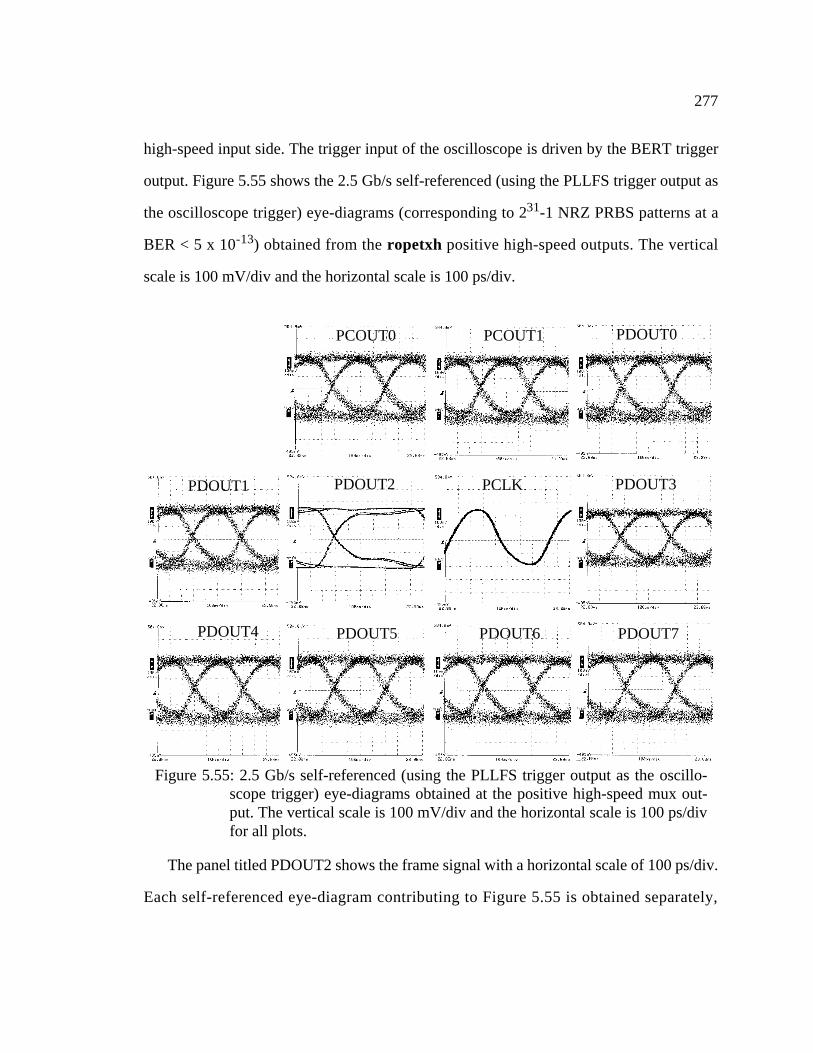
277
high-speed input side. The trigger input of the oscilloscope is driven by the BERT trigger
output. Figure 5.55 shows the 2.5 Gb/s self-referenced (using the PLLFS trigger output as
the oscilloscope trigger) eye-diagrams (corresponding to 231-1 NRZ PRBS patterns at a
BER < 5 x 10-13) obtained from the ropetxh positive high-speed outputs. The vertical
scale is 100 mV/div and the horizontal scale is 100 ps/div.
The panel titled PDOUT2 shows the frame signal with a horizontal scale of 100 ps/div.
Each self-referenced eye-diagram contributing to Figure 5.55 is obtained separately,
PDOUT4
PDOUT1
Figure 5.55: 2.5 Gb/s self-referenced (using the PLLFS trigger output as the oscillo-scope trigger) eye-diagrams obtained at the positive high-speed mux out-put. The vertical scale is 100 mV/div and the horizontal scale is 100 ps/divfor all plots.
PCOUT0
PDOUT2
PDOUT5
PCOUT1
PCLK
PDOUT6 PDOUT7
PDOUT3
PDOUT0

278
without adjusting the clock-to-data setup time at the high-speed input side and using the
trigger output of the ropetxh IC for the oscilloscope trigger input.
The 600 mV slow-speed output voltage setting on the roperxh IC is used for the slow-
speed loopback test. Representative demultiplexed slow-speed (source and load
terminated) output eye-diagrams of the roperxh IC at the slow-speed loopback interface
for the setup in Figure 5.38 are shown in Figure 5.56. These eye-diagrams correspond to
2.5 Gb/s 231-1 NRZ PRBS injected into the high-speed inputs of the roperxh IC. The eye-
diagrams in Figure 5.56 (HSCNTRL11-14), correspond to the high-speed data input
PDIN7. Each eye-diagram corresponds to a single-ended data rate of 625 Mb/s. The
roperxh differential slow-speed clock outputs (D14_OUT_P and D14_OUT_N) are also
shown in Figure 5.56. The horizontal scale for all panels in Figure 5.56 is 500 ps/div and
Figure 5.56: Representative demultiplexed eye-diagrams of PDIN7 at 625 Mb/s/channel at the slow-speed outputs of the roperxh IC in Figure 5.38.D14_OUT_P and D14_OUT_N correspond to the half-speed clockoutputs of the roperxh IC. The horizontal scale for all plots is 500ps/div and vertical scale is 50 mV/div for all plots.
HSCNTRL11 HSCNTRL12 HSCNTRL13
HSCNTRL14 D14_OUT_P D14_OUT_N

279
the vertical scale is 50 mV/div. Figure 5.57 shows the roperxh IC high-speed input clock-
to-data phase-margin of the innermost channel (PDOUT1, diamonds) and the outermost
channel (PCIN0, squares) measured in electrical-loopback on the slow-speed side. The
innermost channel (PDOUT1) is adjacent to the clock channel (PCLK) and the outermost
channel (PCIN0) is furthest from the clock channel. The input clock-to-data phase-margin
is approximately 200 ps at a BER < 10-13. It is practically the same for the innermost and
outermost channels.
Figure 5.58 (a) shows the source (input-clock) referenced jitter measurement of the
innermost (adjacent to the clock channel) data channel PDOUT3 and the outermost and
the outermost (furthest from the clock channel) data channel PDOUT7. The jitter
measurements correspond to the eye-diagrams shown in Figure 5.54. The jitter is
measured to be 13.49 ps rms (94 ps peak-to-peak) and 13.89 ps rms (113 ps peak-to-peak)
respectively. The corresponding self-referenced jitter (shown in Figure 5.59) is measured
Figure 5.57: Variation of the roperxh IC high-speed input clock-to-data phase-mar-gin for the outermost (squares) and the innermost (diamonds) input chan-nels measured in electrical loopback on the slow-speed side.

280
to be 14.45 ps rms (105 ps peak-to-peak) and 14 ps (111 ps peak-to-peak) for (a)
PDOUT3+ and (b) PDOUT7+ respectively.
The source- and self-referenced jitter statistics of high-speed outputs PCOUT0+
(outer left channel), PDOUT1+ (data channel adjacent to clock channel), PDOUT2+
(frame channel), PCLKOUT+ (high-speed clock output), PDOUT3+ (data channel
adjacent to clock channel) and PDOUT7+ (outer right channel) are tabulated in Table 5.5
(a) (b)
Figure 5.58: Source-referenced jitter statistics of (a) PDOUT3+ and (b) PDOUT7+.The horizontal scale is 50 ps/div for both (a) and (b).
100
mV
/div
100
mV
/div
(a) (b)
Figure 5.59: Self-referenced jitter statistics of (a) PDOUT3+ and (b) PDOUT7+.The horizontal scale is 50 ps/div for both (a) and (b).
100
mV
/div
100
mV
/div

281
for the electrical slow-speed loopback test. These jitter measurements correspond to 231-1
NRZ PRBS input data patterns which are injected into the roperxh high-speed input from
the BERT. The PCLKOUT+ jitter in Table 5.5 is higher than the jitter tabulated in entry 9
in Table 5.4 because it is measured at the same horizontal scale of 50 ps/div and vertical
scale of 100 mV/div as the data channels, incurring a slope error in the jitter statistics
measurement.
Figure 5.60 shows the variation of the high-speed output phase-margin of the
innermost (PCOUT0, diamonds) and the outermost channel (PDOUT1, squares) measured
in electrical-loopback on the slow-speed side. The output phase-margin is better than 200
ps at a BER < 10-13. It is practically the same for both the outermost and innermost data
channels. Figure 5.61 shows the eye-diagram of each data output channel with an overlay
of the high-speed clock. The vertical scale is 100 mV/div and the horizontal scale is 100
ps/div. PDOUT7 and PCOUT0 are the outermost channels (furthest from the clock
channel). PDOUT3 and PDOUT2 are the innermost channels (adjacent to the clock
Channel
RMS Source-
referenced Jitter (ps)
Peak-to-peak Source-
referenced Jitter (ps)
RMS Self-referenced Jitter (ps)
Peak-to-peak Self-
referenced Jitter (ps)
PCOUT0+ 15.81 102 14.35 103
PDOUT1+ 15.24 111 13.7 92
PDOUT2+ 6.99 53 6.5 43
PCLKOUT+ 7.18 55 5.27 40
PDOUT3+ 13.49 94 14.45 105
PDOUT7+ 13.89 113 14 111
Table 5.5: Measured output jitter for different channels in slow-speed loopback.

282
channel). The overlaid clock corresponds to the nominal position for successful error-free
DC-coupled loopback on the high-speed side for all channels.
Figure 5.62 (a) shows the measured skew of 5 ps between the outermost channels
PDOUT7 and PCOUT0. Figure 5.62 (b) shows the measured skew of 25 ps between the
one of the outermost channels, PCOUT0 and one of the innermost channels, PDOUT3.
PDOUT7 and PCOUT0 are not displayed in Figure 5.62 (a) and (b) respectively for
clarity. The skew measurements account for the total delay of the cables, PCB and QFP
traces, and oscilloscope sampling-heads, which is measured to be less than 2 ps.
Figure 5.60: ropetxh high-speed output phase-margin for the innermost (PDOUT1,diamonds) and outermost (PCOUT0, squares) channels measured inelectrical loopback on the slow-speed side.

283
PDOUT7+
PDOUT6+
PDOUT5+
PDOUT4+
PDOUT3+
PDOUT2+
PDOUT1+
PDOUT0+
PCOUT1+
PCOUT0+
Figure 5.61: Overlaid high-speed data and clock eye-diagrams for each high-speedoutput corresponding to 231-1 NRZ PRBS patterns. The horizontalscale is 100 ps/div and the vertical scale is 100 mV/div for all plots.
(a) (b)
Figure 5.62: Skew (a) of 5 ps the outermost channels PDOUT7 (not displayed inpanel) and PCOUT0 and (b) 25 ps between the outermost channelPCOUT0 (not displayed in panel) and the innermost channel PDOUT3.The horizontal scale is 50 ps/div for both (a) and (b).
100
mV
/div
100
mV
/div

284
5.6.7 Optical Loopback Measurements
Optical loopback measurements are performed using the Agilent Tx and Rx parallel
optical link modules [216], which are mechanically fixtured on distinct evaluation boards.
The average light output power of each optical Tx channel was measured using an
Agilent 81520A 450 nm to 1020 nm detector, connected to an Agilent 8153A lightwave
multimeter. The measured average light output power corresponding to logic high at any
optical Tx channel output was measured to be between 430 µW and 498 µW. The
Channel 9
Channel 3
Channel 7
Channel 11
Channel 5
Figure 5.63: Source-referenced PONI Tx-Rx 2.5 Gb/s optical eye-diagrams measured(using the BERT trigger output as the oscilloscope trigger) at the positivehigh-speed optical outputs. The vertical scale is 100 mV/div and the hori-zontal scale is 100 ps/div for all eye-diagrams.
Channel 1
Channel 10
Channel 6
Channel 2
Channel 12
Channel 8
Channel 4

285
measured average light output power corresponding to logic low at any optical Tx channel
output was measured to be between 3 µW and 4 µW. Optical loopback measurements are
performed on the Tx and Rx parallel optical link modules after connecting a 12-wide
fiber-optic ribbon between the Tx and Rx modules. Figure 5.63 shows the source-
referenced (BERT triggered) eye-diagrams of the output of each PONI Rx module
channel in optical loopback. Each eye-diagram in Figure 5.63 corresponds to ac-coupled
231-1 NRZ PRBS input data patterns with an amplitude of 400 mV, which are injected
into the Tx module from a BERT at 2.5 Gb/s.
The jitter measurements of channel 1 (outermost channel) and channel 6 (innermost
channel) are shown in Figure 5.64. The jitter is measured to be 17.7 ps rms (120 ps peak-
to-peak) and 18.2 ps rms (126 ps peak-to-peak) for channels 1 and 6 respectively. The
measured jitter of each channel in optical loopback with data driven from the BERT is
tabulated in Table 5.5, along with the measured jitter of each channel, when the parallel
optical Tx module in Tx-Rx optical loopback is driven by the high-speed outputs of the
slow-speed electrical loopback, shown in Figure 5.65.
(a) (b)
Figure 5.64: Source-referenced jitter statistics of the Rx module output of channel 1and channel 6 in the optical loopback setup, with a BERT as the electri-cal data source driving the Tx module inputs. The horizontal scale is 50ps/div and the vertical scale is 50 mV/div for both (a) and (b).
50 m
V/d
iv
50 m
V/d
iv

286
It can be seen that the jitter contribution to the data outputs of the ropetxh IC in
optical loopback is dominated by the jitter contribution of the Tx-Rx POSA modules. This
jitter contribution needs to be addressed in order to improve the robustness of parallel
optical data links for data rates in excess of 2.5 Gb/s/channel.
The high-speed outputs of the ropetxh IC in the slow-speed electrical setup (Figure
5.38) are ac-coupled to the parallel optical Tx module through bias-tees as shown in
Figure 5.65. The parallel optical Rx module outputs are connected to the BERT to
measure the BER and to the oscilloscope to plot the eye-diagrams. The source-referenced
Channel #
Source-ref. rms jitter (ps) with BERT driving parallel optical
Tx module input.
Source-ref. peak-to-peak jitter (ps)
with BERT driving parallel
optical Tx module input.
Source-ref. rms jitter (ps) with electrical loop-back
output driving parallel optical Tx module input.
(Figure 5.65)
Source-ref. peak-to-peak jitter (ps) with electrical loop-back output driving
parallel optical Tx module input (Figure 5.65).
1 17.7 120 Not used Not used
2 21.74 146 19.54 143
3 16.6 117 18.93 149
4 18.04 137 18.7 143
5 18.08 159 21.29 153
6 18.2 126 8.3 62
7 17.89 129 12.36 94
8 16.1 126 20.1 140
9 20.02 142 20.91 157
10 17.06 137 21.61 163
11 12.48 99 20.82 158
12 15.62 109 18.38 133
Table 5.6 Measured jitter of each parallel optical Rx module output.

287
(BERT trigger output connected to oscilloscope trigger input) eye-diagrams for the 11
parallel optical Rx module outputs corresponding to the roperxh IC high-speed outputs
(including frame (PDIN2) and clock (PCLK)) are shown in Figure 5.66. Each eye-
diagram corresponds to a 231-1 NRZ PRBS input data pattern at a BER < 5 x 10-13. The
frame channel (PDIN2) has a larger horizontal scale of 500 ps/div instead of the horizontal
scale of 100 ps/div for all the other channels in order to show the entire frame signal.
The source-referenced jitter statistics of PDOUT7+ (outermost channel) and
PDOUT3+ (innermost channel) corresponding to the eye-diagrams in Figure 5.66, are
shown in Figure 5.67. The measured jitter of PDOUT7+ and PDOUT3+ are 20.1 ps rms
1:49
1 diff. line
Clock
MUX
inputs
BERT Power Splitters
DEMUX IC (roperxh)
4:1
10
DEMUX
outputs
2 feetof 3MRG178SCIcable
1/4
9
+
-
1 diff. line
1 diff. line
1/4
1.75V
1.75V
1/2
2 Frame
x4 PLLFS
10Tx POSAwith T40 module
Rx POSAwith R64 module(HRX2112)
Fiber-Optic Ribbon
Figure 5.65: Schematic of the slow-speed loopback setup with optical loopbackusing the Agilent parallel optical Tx and Rx modules driven by the high-speed output of the ropetxh IC. Note that all the BER measurements aresource-referenced.
To Oscilloscope
9
9
9
MUX IC (ropetxh)

288
(140 ps peak-to-peak) and 20.2 ps rms (145 ps peak-to-peak) respectively. The self-
referenced (PLLFS trigger output connected to oscilloscope trigger) jitter statistics of the
parallel optical Rx module outputs corresponding to PDOUT7+ (outermost) and
PDOUT1+ (innermost) is shown in Figure 5.68. The measured jitter of PDOUT7+ and
PDOUT1+ is 20.4 ps rms (168 ps peak-to-peak) and 20.62 ps rms (154 ps peak-to-peak)
respectively.
PDOUT4
PDOUT1
PCOUT0
PDOUT2
PDOUT5
PCOUT1
PCLK
PDOUT6
Figure 5.66: Source-referenced 2.5 Gb/s optical eye-diagrams measured (using theBERT trigger output as the oscilloscope trigger) at the positive high-speed optical Rx module outputs. The vertical scale is 50 mV/div andthe horizontal scale is 100 ps/div.
PDOUT7
PDOUT3
PDOUT0

289
.
(a) (b)
Figure 5.67: Source-referenced jitter statistics of the optical Rx module correspond-ing to PDOUT3+ and PDOUT7+. The vertical scale is 50 mV/div andthe horizontal scale is 100 ps/div for both (a) and (b).
50 m
V/d
iv
50 m
V/d
iv
(a) (b)
Figure 5.68: Self-referenced jitter statistics of the optical Rx module outputs corre-sponding to PDOUT1+ and PDOUT7+. The horizontal scale is 50 ps/div and the vertical scale is 50 mV/div for both (a) and (b).
50 m
V/d
iv
50 m
V/d
iv

290
5.7 Test Setup limitations
All measurements in this chapter include the detrimental effects of the evaluation
printed circuit board (PCB), fixturing, connectors, and cabling frequency response.
Without these effects, the measured IC sensitivity would be significantly improved.
Figure 5.69 shows the results of the insertion-loss measurements representative of the
evaluation board setup. Typical insertion-loss at 2.5 Gb/s (1.25 GHz) is between 6 and 7
dB with a -3 dB bandwidth between 700 MHz and 750 MHz. Figure 5.69 (a) shows the
insertion-loss of the slow-speed evaluation board which includes, in order, 10” of 3M SCI
cable, an evaluation PCB trace, the PONI MUX QFP trace and wire bonds, another
evaluation PCB trace and another 10” of 3M SCI cable. Figure 5.69 (b) shows the
insertion-loss of the evaluation board from the slow-speed to the high-speed side through
a 7 mm long transmission line on a ceramic through insert in the PONI MUX QFP cavity.
The setup includes, in order, 10” of 3M SCI cable, an evaluation PCB trace, the PONI
MUX QFP trace and wire bond, a 7 mm long ceramic transmission line, another PONI
MUX QFP trace and wire bond, another evaluation PCB trace and another 10” of 3M SCI
cable. Figure 5.69 (c) shows the insertion-loss of the evaluation board for the high-speed
(b) (c)
Figure 5.69: Insertion-loss measurement of (a) slow-speed side evaluation board,(b) slow-speed side to high-speed side evaluation board and (c) high-speed side evaluation board.
(a)

291
side. The setup includes, in order, 10” of 3M SCI cable, an evaluation PCB trace, the
PONI MUX QFP traces and wire bonds, another evaluation PCB trace and another 10” of
3M SCI cable.
5.8 Summary
We utilized the key components of high-speed flop-flops, multiplexers, receivers,
transmitters, low-output impedance clock buffers and the low-skew clock distribution
circuitry in Chapter 3 to demonstrate a 1:4/4:1 mux/demux BER circuit in 0.5 µm CMOS
that achieved 2.80 Gb/s at a BER < 10-13 for 231 - 1 NRZ PRBS data patterns. The results
from the 1:4/4:1 demux/mux BER circuit and the clock distribution technique in Chapter 3
(Section 3.7.8 on page 105) inform the demonstration of a 12-wide 2.5 Gb/s/channel 1:2/
2:1 mux/demux array that achieves an edge-connection data-bandwidth density of 55 Gb/
s/cm. The validation of the above components, along with the low-jitter wide-range x4
PLLFS in Chapter 4, was key to the demonstration of an 8.8 W, 11-channel 2.5 Gb/s/
channel half-speed 4:1/1:4 multiplexer/demultiplexer chipset with an integrated sub-50 ps
peak-to-peak jitter x4 PLLFS at 1.25 GHz in relatively modest 0.5 µm CMOS process
technology. The integrated x4 PLLFS is capable of operation from 0.4 to 1.6 GHz. The
chipset achieves an edge-connection data-bandwidth density of 50 Gb/s/cm, which is a
factor of 12.7 better than the flex connector interface used to connect the system board and
IO board in the state of the art HP 785/J7000 Forte workstation.The skew of the interface
was measured to be better than 25 ps. The introduction of jitter by the opto-electronic
components in a parallel optical data link was determined to dominate the jitter of the
high-speed output interface (2.5 Gb/s/channel) of the chipset in optical loopback. This
jitter contribution needs to be addressed in order to improve the robustness of parallel
optical data links for data rates in excess of 2.5 Gb/s/channel.

292
5.9 Acknowledgments
We gratefully acknowledge Young-Gook Kim’s assistance in the fabrication of the
ceramic inserts and the layout of the PONI MUX QFP evaluation board used in the
measurements of the PONIMUX IC.

293
Chapter 6
Parallel Opto-Electronic Link Design
We have discussed the components of a 2.5 Gb/s/channel 0.5 µm CMOS parallel
electrical data link in Chapters 3, 4 and 5. The components are electrical receive and
transmit circuits (Chapter 3), a low-jitter wide-range x4 PLLFS (Chapter 4), and an N:1/
1:N multiplexer/demultiplexer arrays (Chapter 5). In order to implement a parallel Opto-
Electronic (OE) data link as shown in the block diagram of an Opto-Electronic System
(OES) in Figure 6.1, we have to demonstrate a 2.5 Gb/s/channel OE transmitter and
receiver array in 0.5 µm CMOS. In Section 6.1, we demonstrate that the electrical transmit
circuit architecture in Section 3.10 on page 114 can also function as a 2.5 Gb/s high-
performance VSCEL diode driver with no errors. The VCSEL driver circuit in 0.5 µm
CMOS consumes up to ten times less power than a conventional electronic PECL [9]
interface circuit and up to five times less power than a conventional electronic LVDS
interface circuit [20]. In Section 6.3, we discuss possible parallel OE receiver architectures
and utilize receiver noise analysis to identify the best receiver front-end design for a 2.5
Gb/s/channel OE receiver array in 0.5 µm CMOS with -20 dBm sensitivity, for the least
power dissipation.

294
We factor in considerations of substrate and power-supply noise injection, operation
across process variations and biasing considerations which constrain parallel receiver
architecture and circuit design. The analysis used to arrive at the 0.5 µm CMOS design
choice is extended to determine the feasibility and the determinant variables of a -20 dBm
10 Gb/s/channel OE receiver array in 0.1 µm CMOS in Chapter 7.
Electrical IO (LVDS, GTL, GLVDS)
VCSEL Array
Sour
ce C
lock
MM
mN
MN
MN MN
Con
trol
Optional Datapath
Rx Bridge Tx Bridge
φ F1/
kN
φF1
φF1/N
φF1/kN
φF1/kN
clockdata
Figure 6.1: Correspondence of discussion in this chapter to the OES IC block dia-gram in Figure 1.10.
1:N demux array
Aligner circuit.
Chapter 6
N:1 Mux array
Chapter 6
φF1/N
Laser Driver ArrayOE Pre-amplifier Array
Decision Circuit Array
xkN PLLFS
PIN Diode Array

295
6.1 VCSEL Driver Design
The Transmit (Tx) circuit is implemented as a differential current-source driver
(Figure 3.53 in Section 3.10 on page 114) with no source termination. Current-source
drive is important for driving low threshold-current VCSELs because it removes the time-
constant associated with the series resistance (which is typically greater than 100 Ω) of the
VCSEL. Care has to be taken to make sure that the current-source drive does not damage
the VCSEL.
Figure 6.2 (a) and (b) show the AC-schematic of an electrical current-source driver
and voltage-source driver respectively, switching on the VCSEL diode1. A current-source
driver is defined as one whose output impedance is much greater (usually by a factor of
ten) than the load impedance. Accordingly, the impedance of the current-source driver
(which would been a resistor in parallel with the current source) is not shown in Figure 6.2
(a). Similarly, a voltage-source driver is defined as one whose output impedance is much
less than that of the load impedance (usually by a factor of ten). Accordingly, the source
impedance is not shown in Figure 6.2 (b).
1. Assuming on-off modulation of the VCSEL diode.
+-
+-Rs
CJ
Rs
CJ
IacIac
Vac VacVo
Vo
+
-
+
-(a) (b)
Figure 6.2: AC-schematic of VCSEL (a) current drive and (b) voltage drive. Rs isthe VCSEL series resistance and CJ is the VCSEL capacitance.

296
The VCSEL diode is represented as a series resistance Rs (which represents the oxide-
confined VCSEL input resistance) and the junction capacitance of the forward biased
diode. This series resistance is currently of the order of 200 ohms for micro-lasers reported
in the literature [22]. These micro-lasers have very low threshold-currents (< 200 µA) and
low breakdown-voltages (< 3V). The large series-resistance introduces a large time-
constant at the VCSEL, preventing ISI-free efficient modulation at high data rates. Figure
6.2 (a) shows the AC-schematic of an electrical current-source driver turning on a VCSEL
diode, assuming that a loss-less switch between the current-source and the VCSEL diode
was closed at time t = 0. The variable of interest is the voltage Vo across CJ. Since the
driver is modeled as a current source, the controlling equation is KCL, which allows the
rate of change of Vo across CJ to be independent of Vo. Therefore, we see that
Iac = CJ dVo/dt (6.1)
giving a linear relationship between Vo and Iac, independent of Rs.
When the source is modeled as a voltage source, the controlling equation is Kirchoff’s
Voltage Law (KVL), which results in the rate of change of Vo being given by RsCJ dVo/dt
+ Vo = Vac. The solution to this equation is an exponential equation which converges to
Vac with a time-constant of RsCJ. The design constraint on the implementation of a
current-source driver is that the voltage drop across the current source when the VCSEL is
on, is sufficient to keep the circuit implementing the current source operating as a current
source. The voltage drop across the current-source driver when the VCSEL is on is given
by VDD - Vfb + IacRs, where Vfb is the forward bias voltage across the VCSEL, which is
typically between 1.5 V and 1.7 V. For Vdd < 3.0V, the CMOS device and circuit
requirements for technologies with feature size less than or equal to 0.25 µm in
conjunction with Vfb, will mandate the presence of a second power supply (negative
supply for common n-substrate VCSEL arrays or positive (> Vdd) supply for common p-

297
substrate VCSEL arrays). Therefore, the implementation of a current source driver for
ultra-low threshold VCSEL diodes should be feasible for scaled CMOS technologies. It is
also to be noted that this has to be balanced with the consideration that the DC-voltage at
the output of the VCSEL driver does not exceed the safe operating potential difference
between any two terminals of the output transistor(s) of the CMOS driver circuit. This safe
potential difference is usually not much larger than the power-supply voltage. Therefore,
the series resistance Rs cannot be too large, as the product of Rs and the current required to
turn on the VCSEL diode may mandate a negative power-supply in order to keep the
output transistors in saturation. When the VCSEL diode is turned off, the safe potential
difference between any two terminals of the output transistor(s) is exceeded because of the
presence of a large negative power supply instead of ground at the terminal of the VCSEL
diode, which is not connected to the current-source output driver.
6.1.1 0.5 µm CMOS VCSEL Driver Measurements
Figure 6.3 (a) shows the schematic of the VCSEL driver circuit, which consists of a
cascade of a receiver circuit (“Rx” in Figure 6.4 (a)), a buffer-amplifier circuit (“Buf” in
Figure 6.3 (a)), and the VCSEL driver circuit (“Tx” in Figure 6.3 (a)). The circuit
schematics of the Rx (and Buf, which has the same circuit schematic as Rx) and Tx are
shown in Figure 3.49 and Figure 3.53 respectively. Figure 6.3 (b) shows the output eye-
diagram of the Rx-Tx circuit for a 3.3 Gb/s 231 - 1 NRZ PRBS input data stream with an
amplitude of 200 mV. The vertical scale is 200 mV/div and the horizontal scale is 50 ps/
div.
The small-signal response in Figure 6.3 (c) is the single-ended insertion-gain
measurement showing a measured -3 dB bandwidth of 1.7 GHz. The small-signal
insertion-gain measurement is done by injecting +3.0 dBm of power through a bias-tee
from an Agilent 85645A tracking source into the positive input of the Rx circuit and

298
measuring the response of the output through a bias-tee using an Agilent 8564E spectrum
analyzer. Bias-tees are used so that the inputs and outputs of the Rx and Tx circuits are
properly biased.
The Receiver (Rx) and buffer circuits each consume 10 mA, and the Tx circuit
consumes 11.7 mA from a 3.6 V power supply, 8mA of which is sent into the link (i.e.,
down the transmission lines into the 50 Ω resistor terminated to VTT). The measured
electrical BER tests of the circuit shown in Figure 3.46 indicate a data rate of 3.3 Gb/s
(300 ps bit period) for Vin = 200 mV, Vdd = 3.60 V, VTT = 1.75V with BER < 10-12 is
possible. The eye-width of the output is 223 ps at a BER < 10-3 and the eye-height is 100
mV. The rise- and fall-times of the electrical outputs are 116 ps and 160 ps respectively.
The input sensitivity decreases to 50 mV for input data rates below 3.0 Gb/s. The power
consumption of the complete electrical link is 99.76 mW (3.6 V X (10 mA + 10 mA + 3.7
mA) + (3.6 - 1.75) V X 8.0 mA = 99.76 mW).
Schematic of circuit whose small-signal response is shown. VTT = 1.55 V.
Rx Tx Buf
VTT50Ω
50Ω
3.3 Gb/s
Figure 6.3: (a) Schematic of VCSEL driver circuit whose eye-diagram at 3.3 Gb/scorresponding to 231 - 1 NRZ PRBS from the BERT is shown in (b).The measured insertion-gain is shown in (c). See text for details.
(a)
(b)
(c)

299
The laser diodes available for the experiment are low threshold-current oxide-confined
VCSELs from Agilent Technologies [103] with emission wavelength at λ = 850 nm. Laser
diode (LD) L1 has threshold current Ith = 0.5 mA and threshold voltage Vth = 1.5 V. Laser
diode L2 has Ith = 0.2 mA and Vth = 1.5 V. The positive output of the transmit circuit
(“Tx” in Figure 6.3 (a)) is used to drive the VCSEL and the negative output of the Tx
circuit is connected to a sampling oscilloscope via a bias-tee. The optical output of the
VCSEL is collected using a lensed multi-mode fiber and measured with an optical
receiver which has a -3 dB bandwidth of 1.67 GHz. The eye-diagrams in Figure 6.4 and
Figure 6.5 correspond to 231 - 1 NRZ PRBS 50 mV input data patterns. In these Figures,
the eye-widths and the eye-heights are measured at a BER < 10-3. The displayed eye-
diagrams have a measured BER < 10-13.
Figure 6.4 shows the detected error-free eye-diagram for L1 driven by the BERT with
2.5 Gb/s 231 - 1 NRZ PRBS at steady-state bias current of 1.83 mA and bias voltage of
1.7 V. Figure 6.5 shows the electrical (lower trace) and detected optical (upper trace) eye-
diagrams of the Tx circuit coupled to L1 through an interposing 13 dB attenuator at the L1
end and operating at 2.5 Gb/s (400 ps bit period).
Figure 6.4: 2.5 Gb/s 231 - 1 NRZ PRBS eye-diagram for LD L1 driven by BERT.

300
The electrical output is displayed after attenuation by a 20 dB attenuator. The vertical
scale is same for both traces. Input data is 50 mV 2.5 Gb/s 231 - 1 NRZ PRBS. The steady-
state bias current of L1 is 1.932 mA at a voltage bias of 1.7 V. The measured average light
output of L1 is 372 µW at this operating point. The signal current delivered into L1 has a
measured peak-to-peak value of 1.6 mA2. The detected optical output has an eye-width of
295 ps and an eye-height of 55 mV. The electrical output has an eye-width of 313 ps and
an eye-height of 163 mV.
Figure 6.6 shows the electrical (lower trace) and detected optical (upper trace) eye-
diagrams of the Tx circuit coupled to L2 through an interposing 20 dB attenuator at the L2
end and operating at 1.25 Gb/s (800 ps bit period). The electrical output is displayed on
the oscilloscope after attenuation by a 20 dB attenuator prior to display. The vertical scale
is the same for both traces. The input data is a 50 mV 1.25 Gb/s 231 - 1 NRZ PRBS
2. Measured by a Tektronix current sensor with 5 mV/mA sensitivity insertedbetween the 20 dB attenuator and L1.
Figure 6.5: 2.5 Gb/s 231 - 1 NRZ PRBS eye-diagram for LD L1 (top waveform) andelectrical output (lower waveform).
100 ps/div
200
mV
/div

301
pattern. The time-averaged bias current of L2 is 0.48 mA at a voltage bias of 1.6 V. The
measured average light output of L2 is 38.9 µW at this operating point. The measured
signal current delivered into L2 is 336 µA peak-to-peak. The detected optical output has
an eye-width of 614 ps and an eye-height of 138 mV. The electrical output has an eye-
width of 738 ps and an eye-height of 288 mV.
A differential Tx circuit delivering the 1.6 mA signal current required to drive L1 at
2.5 Gb/s consumes 1.16 mA for the pre-driver and has a total power consumption of 7.22
mW, which is approximately one fourth of the power consumed by the Tx circuit for the
LVDS electrical case (see earlier discussion on page 298). A differential Tx circuit
delivering the 336 µA signal current required to drive L2 at 1.25 Gb/s consumes 242.6 µA
for the pre-driver, and has a total power consumption of 1.50 mW.
Our experimental results indicate that compared to electrical LVDS output drivers, the
power consumption of the CMOS optical Tx circuitry can be reduced by a factor of better
than 4 while driving the low threshold-current oxide-confined VCSEL L1 at 2.5 Gb/s and
200 ps/div
200
mV
/div
Figure 6.6: 1.25 Gb/s 231 - 1 NRZ PRBS eye diagram for LD L1 (top wave-form) and electrical output (lower waveform).

302
by a factor of 20 while driving the low threshold-current oxide-confined VCSEL L2 at
1.25 Gb/s. The measured minimum electrical sensitivity of the electrical Rx circuit is 50
mV at 2.5 Gb/s and 10 mV at 1.25 Gb/s. This means that a 500 Ω transimpedance
amplifier (TIA) for the case of L1 and a 960 Ω amplifier for the case of L2 is required for
a complete CMOS OE link, assuming a conversion efficiency of 0.55 for the photo-diodes
and an optical link-loss of 6 dB. In conclusion, we have demonstrated experimentally that
low threshold-current oxide-confined VCSELs can be driven by a low-power CMOS
circuit at high data rates. A CMOS laser-diode driver has a power consumption that is a
factor of 20 less than that of a PECL electrical transmit circuit and a factor of 4 less than
that of an LVDS transmit circuit at 2.5 Gb/s in 0.5 µm CMOS. This reduction in power
dissipation makes it feasible to achieve a power consumption advantage even when the
CMOS transimpedance amplifiers are factored in. This enables future efficient integration
of CMOS and parallel OE data links while retaining the inherent distance-bandwidth
product and form-factor advantage of optical interconnects.
6.2 System Perspective on an OE Link
So far, we have discussed a CMOS VCSEL driver in 0.5 µm CMOS process
technology. The reduction in power dissipation comes with the penalty of a relatively low
optical output power. Unless the VCSEL output is constrained to be in a box preventing
the VCSEL output from accidentally reaching a human eye, the VCSEL output power has
to be less than the maximum specified optical output power at the emission wavelength of
the VCSEL. The safe optical output power decreases with wavelength because the retina
is more likely to be damaged at lower optical power for shorter wavelengths. In addition,
connector loss, VCSEL device variations during fabrication, ageing, and link-loss among
other factors, reduce the optical power reaching the optical transducer.

303
We compare an electrical link consisting of the CMOS electrical Rx and Tx discussed
earlier, and an OE link consisting of a CMOS VCSEL driver and an OE receiver. We take
into account the low VCSEL optical output power and the link-loss that is sustained in
each case. An examination of a conventional Electro-Optic (EO) - (OE) link indicates that
an OE data link will attenuate the input electrical power by a factor as large as 100. This
attenuation is best represented as the ratio of the received OE transducer current to the
current output of the transmitter expressed in dB, which we shall call the Link
Transmission Figure (LTF). The OE receive circuit in the link consumes additional power
to combat the link-loss indicated by the LTF.
Figure 6.7 shows the EO-OE link characteristics for a typical OE data link at 2.5 Gb/s
with ultra-low threshold VCSEL L1 described above. The power delivered to L1 is the
product of the measured current delivered to L1 and the voltage bias across L1. The power
transfer function (output light power to delivered electric power) is determined from the
measured average light power at the bias point of the VCSEL. A link-loss of 10 dB is
assumed to represent coupling loss, connector loss and loss due to aging of the link. The
conversion efficiency, CE, of the OE transducer, which is assumed to be a PIN diode at
850 nm wavelength with a responsivity3 of 0.8, is 0.85 * 0.8 / 1.24 Amps/Watt = 0.55
Amps/Watt.
3. Energy at 1 µm emission wavelength = hc/λ = hc/1 µm = 1.24 eV where h isplanck’s constant and c is the velocity of light.
-8.64 -10 CE=0.552.72 mW 0.372 mW 0.0372 mW 20.46 µA
LD L1 PINLinkIdc=2.0mAIac=1.6mA
LTF= 20log(Iout/Iin)= -37.86 dB
CASE 1: L1 (850 nm)
L1dB dB
2.5 Gb/s
Figure 6.7: EO-OE LTF for typical OE data link with L1 and 10 db optical link-loss.

304
The Link Transmission Figure (LTF) is defined as the ratio of the current produced by
the OE transducer (a PIN diode in this case) to the ratio of the current delivered to the
VCSEL by the VCSEL driver, in dB (electrical). In other words, LTF = 20*log(Iout/Iin).
A factor of 20 is used instead of 10 to multiply the logarithm because the objective of this
measure is to represent the OE data link by a two-port circuit element with the transfer
function (usually loss) for inclusion in electrical circuits. A dB representation in electrical
circuits is usually for power and has a factor of 20 multiplying the logarithm of the ratio of
voltages or currents. From these considerations, the LTF in Figure 6.7 is -37.86 dB. Figure
6.8 shows the LTF for the OE data link with L2 and the measured, delivered input current
and the average optical output power, with an assumed link-loss of 10 dB (optical) and a
CE of 0.55 for the opto-electric transducer. The calculated LTF is 44 dB.
In contrast, the electrical link interconnect for the Rx-Tx circuits described here can
sustain a maximum link-loss of 19 dB at 2.5 Gb/s because the input sensitivity of the Rx
circuit is 50 mV. The LTF for this case is -19 dB. The Tx circuit consumes 42 mW and the
Rx circuit consumes 38 mW for a total power consumption of 80 mW for operation at 2.5
Gb/s. The interconnects presented so far can be represented by a linear two-port circuit as
LD L2 PD
564.4 µW 38 µW 3.8 µW 2.09 µACE=0.55-11.7 -10
LinkIdc = 0.5 mAIac = 0.34 mA
LTF = 20log(Iout/Iin) = -44.0 dB
CASE 2: L2 (850 nm)
dB dB
1.25 Gb/s
Figure 6.8: EO-OE LTF for a typical OE data link with L2 and 10 dB optical link-loss.
Figure 6.9: LTF of electrical link that can be supported by designed LVDS Rx-Txcircuitry in 0.5 µm CMOS at 2.5 Gb/s.
Interconnect power loss = 19 dB (sustainable)
4.05 mW 50 µW
LTF = 20log(Iout/Iin) = -19 dBElectrical link

305
shown in Figure 6.10. The linear two-port circuit is represented as a current-in current-out
circuit because of the unified perspective we have chosen to impose on the OE and
electrical data links that have been defined. VCSEL diodes are fundamentally current-
controlled devices. OE transducers are fundamentally current output devices (typically
with a logarithmic relationship between the output current and voltage developed across
the transducer). The OE transducer voltage output would suffer from a compression in
dynamic range because it is a logarithm of the current generated by the captured photons.
The linear two-port representation has an input impedance which is representative of
the link. In the case of an ultra-low threshold-current VCSEL, the impedance is a series
combination of Rs and CJ as shown in Figure 6.2 (a). In the case of an electrical link, the
impedance is 50 Ω, representing the AC-impedance of the line. The loss in the link is
represented by α, which is a dimensionless number. α is the LTF expressed as a ratio
instead of in dB terms. Zpar is the impedance at the output terminal of the link. In the case
of an OE data link, this is usually a parasitic capacitance. In order for maximal signal
transfer, the impedance of the source, Zs, must be much greater than the input impedance
of the link, and the impedance of the load, ZL, must be much less than that of the output
impedance of the link, Z4OUT. Here we adopt the principle of maximal mismatch between
4. In intuitive terms, this is the reason that an OE pre-amplifier is usually a TIAwith large open-loop gain A, so that Rf/(1+|A|) << ZOUT for maximum transferof the signal current into the amplifier input, where Rf is the feedback resistanceof the TIA.
Figure 6.10: Linear two-port representation of interconnect.
αil
ilZpar
Zin
Iac
ZOUT ZLZs

306
DC-coupled circuit stages for wideband operation by minimizing the interaction between
stages. The link can now be viewed for purposes of analysis and design as a Current
Controlled Current Source (CCCS), with the purpose of maximizing the current delivered
to the load ZL.
The reduction in transmit power to 7.22 mW (Figure 6.7) and 1.5 mW (Figure 6.8)
does not significantly reduce the power consumption for transmitting data across the OE
data link because the LTF is high in both cases. The loss in the link has to be compensated
by gain in the receiver. In the ideal case, this can be represented as the consumption of
power from the supply to boost the received signal. An LTF of -40 dB implies that an ideal
receiver would consume 40 dB of power from the power supply to deliver 40 dB gain to
the signal. Parasitic elements at the receiver input and the need for standby power
dissipation will force this value to be higher.
The best available implementation of a 0.5 µm CMOS OE Rx that can amplify the
received current is a -20 dBm, 1.25 Gb/s receiver, which consumes 88 mW [25][26]. A
reduction in the LTF from 39.8 dB to 19 dB (making the optical link-loss comparable to
electrical link-loss) will reduce the OE Rx power consumption to 38 mW.
It is obvious that the bulk of the power consumed in the EO - OE link is by the receiver
circuit because of the reduction in the transmit power consumption due to the
development of micro-lasers. The need to overcome the LTF at the receiver side also
increases the power consumption of the receiver circuit. The layout area occupied by the
electrical Tx, electrical Rx circuits and a TIA in 0.5 µm CMOS is tabulated in Table 6.1.
All dimensions are in µm. The OE Rx circuit is a cascade of the TIA and the Rx circuits,
or the Rx circuit in isolation, depending on the received light level. Scaling from 0.5 µm to
0.1 µm results in a 97% reduction in area.
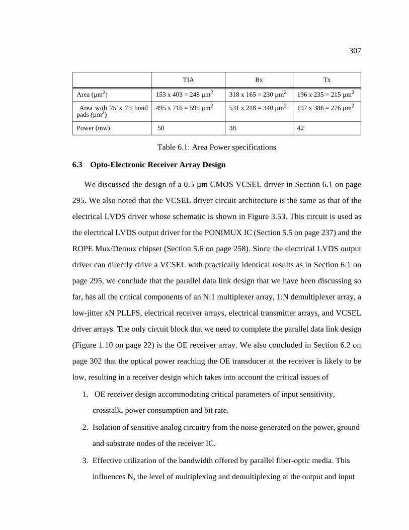
307
6.3 Opto-Electronic Receiver Array Design
We discussed the design of a 0.5 µm CMOS VCSEL driver in Section 6.1 on page
295. We also noted that the VCSEL driver circuit architecture is the same as that of the
electrical LVDS driver whose schematic is shown in Figure 3.53. This circuit is used as
the electrical LVDS output driver for the PONIMUX IC (Section 5.5 on page 237) and the
ROPE Mux/Demux chipset (Section 5.6 on page 258). Since the electrical LVDS output
driver can directly drive a VCSEL with practically identical results as in Section 6.1 on
page 295, we conclude that the parallel data link design that we have been discussing so
far, has all the critical components of an N:1 multiplexer array, 1:N demultiplexer array, a
low-jitter xN PLLFS, electrical receiver arrays, electrical transmitter arrays, and VCSEL
driver arrays. The only circuit block that we need to complete the parallel data link design
(Figure 1.10 on page 22) is the OE receiver array. We also concluded in Section 6.2 on
page 302 that the optical power reaching the OE transducer at the receiver is likely to be
low, resulting in a receiver design which takes into account the critical issues of
1. OE receiver design accommodating critical parameters of input sensitivity,
crosstalk, power consumption and bit rate.
2. Isolation of sensitive analog circuitry from the noise generated on the power, ground
and substrate nodes of the receiver IC.
3. Effective utilization of the bandwidth offered by parallel fiber-optic media. This
influences N, the level of multiplexing and demultiplexing at the output and input
TIA Rx Tx
Area (µm2) 153 x 403 = 248 µm2 318 x 165 = 230 µm2 196 x 235 = 215 µm2
Area with 75 x 75 bondpads (µm2)
495 x 716 = 595 µm2 531 x 218 = 340 µm2 197 x 386 = 276 µm2
Power (mw) 50 38 42
Table 6.1: Area Power specifications

308
ends respectively. The value of N plays a strong role in the achievable jitter on the
IC clock which is synthesized from an incoming slow-speed clock.
4. The optical link-loss, which includes low-loss coupling from multi-mode fiber to
small diameter photo-diodes.
5. The parasitic capacitance associated with the OE transducer, which is the dominant
factor influencing capacitive loading of the input of the OE receiver circuit,
degrading its performance.
Typical optical receivers are divided into two categories: asynchronous receivers and
synchronous receivers. A block diagram of a typical asynchronous receiver is shown in
Figure 6.11. An NRZ signaling format is assumed for all receivers because of its lower
bandwidth requirement compared to RZ or biphase signalling.
Optical signals are received from the transmission medium and converted to an
electronic signal by an OE transducer. The optical signals can be free-space optical signals
or can be coupled into the transducer from a single-mode or multi-mode fiber. The OE
transducer may have some form of internal gain as in an Avalanche Photo-Diode (APD).
The presence of an APD in an OE data link is determined by the choice of the emission
wavelength and the practicality of having the APD bias voltage in the system. The choice
between OE transducers is usually a trade-off between bandwidth and responsivity.
Pre-amp DecisionCircuit
VTh
Channel Filter
Output
Figure 6.11: Block diagram of an asynchronous OE receiver

309
The pre-amplifier amplifies the photodiode signal which may be treated as a current or
a voltage signal and produces an amplified signal which is typically a voltage signal. An
optional channel filter is placed after the pre-amplifier in order to equalize the transmitter-
medium-pre-amplifier5 channel and/or limit the receiver output noise. The former
consideration is to improve the bandwidth and make the output ISI-free, and the latter is to
limit the bandwidth of the receiver circuit to improve the SNR of the amplified signal. The
latter consideration applies when the receiver bandwidth is greater than that of the signal
and the former applies when the receiver bandwidth is approximately the same as that of
the OE transducer signal. Alternately, the channel filter may be absent from the link
because of the cost or the impracticality of implementing the filter in integrated ICs,
especially in parallel links. For analytic purposes, the channel filter can model the
response of the pre-amplifier if the pre-amplifier is treated as a constant gain block.
The output of the pre-amplifier is fed to a decision circuit which makes a decision as to
whether the received signal corresponds to a logic high or a logic low by comparing it to a
threshold voltage. The input signal-swing to the decision circuit is held constant by an
Automatic Gain Control (AGC) circuit so that the signal amplitude at the input of the
decision circuit is nominally independent of the optical power reaching the opto-electric
transducer over a certain input signal dynamic range. The threshold voltage can be
determined dynamically or it can be a fixed voltage. Typically, some form of threshold-
voltage control is required to accommodate the variations in the link due to ageing and
component degradation. The decision circuit can be viewed as a comparator with built-in
hysteresis. Timing errors due to noise on the input signal mandate that the rise- and fall-
5. The medium can be considered non-distorting for all practical purposes in thisdiscussion. The medium can contribute noise but it shall be considerednegligible compared to the electronic Tx/Rx circuits and device noisecontributions.

310
time on the input signal to the comparator or decision circuit be small compared to that of
the bit period, a typical value being 0.17 times the bit-interval [64].
A synchronous receiver shown in Figure 6.12 samples the amplified optical signal in
the middle of the bit-interval and latches it into a flip-flop. The sampling signal is a clock
signal which is typically extracted from the encoded input stream by a clock recovery
circuit. Since the sampling occurs in the middle of the bit, the rise and fall time
requirements are relaxed compared to the case of the asynchronous receiver and can be as
high as 0.6 times the bit interval [64]. In low-noise low-bitrate applications, this means
that the channel-filter bandwidth can be lowered to reduce the noise bandwidth and
improve the sensitivity of the receiver, and that in high-bandwidth applications, the
receiver-bandwidth design requirements are lower, resulting in lower power-consumption
circuits.
The concepts outlined in Figure 6.11 and Figure 6.12 can be extended to form the
block diagram of an OE receiver array in Figure 6.13. This receiver array finds application
in a PODL, which is the same as a parallel electrical data link (see for example, Section
3.1 on page 47) but for the presence of the OE receiver array instead of an electrical
receiver array. The input to the data link consists of N separate data signals and a clock
signal. These optical inputs are converted to electrical signals using synchronous
Pre-amp DecisionCircuit
VTh
Channel FilterOutput
Clock recovery circuit
Figure 6.12: Block level diagram of synchronous optical receiver

311
detection. The distinction between the methods in Figure 6.12 and Figure 6.13 is that there
is no clock recovery circuit in a parallel OE receiver array. Typically, both clock and data
run at the same speed (i.e., half-speed clocked data). If the data rate is significantly less
than the unity gain-bandwidth of the device in the chosen process technology, the clock
can run at twice the data rate so that the data is latched prior to transmission. This
improves the input phase margin of the OE receiver array.
The block diagram of a practical OE receiver array in an integrated parallel OE data
link is shown in Figure 6.14. The output of the parallel OE receiver array is M*N data
channels and 1 clock channel, where M is the degree of demultiplexing in each channel
(M=4 in the example in Figure 6.14). The output data is synchronized with the clock
channel. ff and hff in Figure 6.14 refer to half-speed and one-fourth speed flip-flops. ffl
and hffl refer to their counterparts delayed by half a sampling clock period. The data
(D1....Dn) and clock signals outputs of the OE pre-amplifiers are amplified to drive the
Pre-amp DecisionCircuit
VTh
Optional Channel FilterOutput
Pre-amp
Pre-amp DecisionCircuit
VTh
Optional Channel FilterOutput
Clock
N data channels
Figure 6.13: Extension of synchronous and asynchronous receiver circuitsto parallel synchronous OE data link.
Clock Amplifier circuit

312
data flip-flops. The clock signal is divided to demultiplex the data outputs of the first level
of latches. This can be repeated until the desired degree of demultiplexing is achieved (see
Section 5.1.4 on page 223). Note that the degree of demultiplexing must be exactly the
same as the degree of multiplexing at the transmitter end. Note also that the demultiplexed
outputs of the data channels are aligned with respect to the divided clock in the block
diagram of Figure 6.14. The disadvantage of this method is that the clock channel, which
runs at the same data rate as the data channels or half the bit-rate in Hz, has N times the
load of the data amplifier circuits.
Since data links are specified by their bit rates (bits/s), we determine the relationship
between the Bit Rate (BR) and the individual stage amplifier bandwidth, f-3dBstage. The
overall amplifier bandwidth is given by
(6.2)
Clock Amplifier circuit
Pre-amp
hff
hfflff
ff hff
hffl
1/2
l
DataAmplifiercircuit
Pre-amp
hff
hfflff
ff hff
hffll
DataAmplifiercircuit
Clock
4N dataChannels
Clk
D1
Dn
Figure 6.14: Half-speed optical receiver array schematic with synchronous receivers.
delay cell
Pre-amp
F 3dB overall( )–BR
2-------=

313
Assuming that there are 3 stages of amplification, each with equal f-3dBstage, we get
(6.3)
where n is the number of stages (which is assumed to be equal to 3) and f-3dBstage is the
individual stage bandwidth.
(6.4)
The number of amplifier stages required to drive the clock load is more than the
numbers of amplifier stages in the data channel. This effectively means that the overall
BandWidth6 (BW) of the clock amplifier circuit is less than the overall bandwidth of each
data amplifier circuit. The relationship between the overall gain requirement and
consequent bandwidth limitation can be captured by the following formulation:
6. F-3dBoverall = f-3dBstage , where n is the number of stages, each havingthe same -3 dB frequency f-3dBstage.
F 3dBoverall– f 3dBstage– 21n---
1–n 3=
0.5f 3dBstage–= =
f 3dBstage– 2F 3dBoverall–2BR
2----------- 2BR= = =
21 n⁄ 1–
Figure 6.15: Variation of F-3dBoverall /fu with the number of amplifier stages,n, for overall gain Go of 2, 4, 6 and 8.

314
Let fu be the unity-gain frequency of an individual amplifier stage. Assuming that the
amplifier stage can be designed as a single-pole wideband amplifier, the single pole can be
treated as a pole at fu/Gs, where Gs is the desired stage gain. The designer has a choice of
the number of stages required to achieve the overall gain, Go = Gsn. The resultant
bandwidth, F-3dBoverall, can be expressed as
(6.5)
The ratio F-3dBoverall /fu is plotted against n, the number of stages, as shown in Figure
6.15. It can be seen that the highest overall bandwidth is obtained for a single-stage gain of
2, with the overall BW decreasing with increasing Go. For Go > 10, the number of stages
required to maximize overall bandwidth becomes less and less distinct. Additionally, it
can be seen that the overall bandwidth cannot be greater fu/3 for Go > 10. Taking the
derivative of Equation 6.5 with respect to n to maximize F-3dBoverall /fu (for a desired
overall gain Go), and setting the numerator equal to zero, we get the number of stages n in
Equation 6.8.
(6.6)
(6.7)
(6.8)
F 3dBoverall–fu
Gon----------- 21 n⁄ 1–=
ndd 21 n⁄ 1–( )
nddGo
1 n⁄
=
21 n⁄ 1–( ) 21 n⁄ 2( )log2 Go( )log
---------------------------=
n 1 2⁄( )log
1 2log
Go2log
-----------------–
log
---------------------------------------=

315
Figure 6.16 (a) plots the F-3dBoverall /fu ratio obtained from Equation 6.5 with desired
overall Gain Go. Figure 6.16 (b) plots the number of stages obtained for different values of
overall gain Go for maximum F-3dBoverall /fu (Equation 6.8). It can be seen from Figure
6.16 (a) that F-3dBoverall /fu is less than 0.2 for Go > 12. In practice, n must be an integer.
The bandwidth of the OE transmit circuit is higher that of the OE receive circuit
because the OE receive circuit has to have high gain and low sensitivity in order to
accommodate the link-loss. This asymmetry means that the link cannot be operated at the
maximum data rate that can be sustained by the transmitter circuitry. Since the gain-
bandwidth product is a constant, the fact that the clock signal amplifier gain has to be large
in Figure 6.14 (because of the capacitive load of the clock channel on the parallel OE
receiver array) limits the maximum bandwidth that it can achieve. An alternate
architecture has to be used where the gain-bandwidth requirement on the clock signal
amplifier is relaxed. Using limiting amplifiers removes the constraint of considering the
gain-bandwidth of the entire clock channel. Another approach that might meet this
requirement is shown in Figure 6.17, which is an adaptation of the oversampling receiver
Figure 6.16: Variation of (a) F-3dBoverall /fu maximum with overall gain Goand (b) number of stages n required to achieve it.
(a) (b)
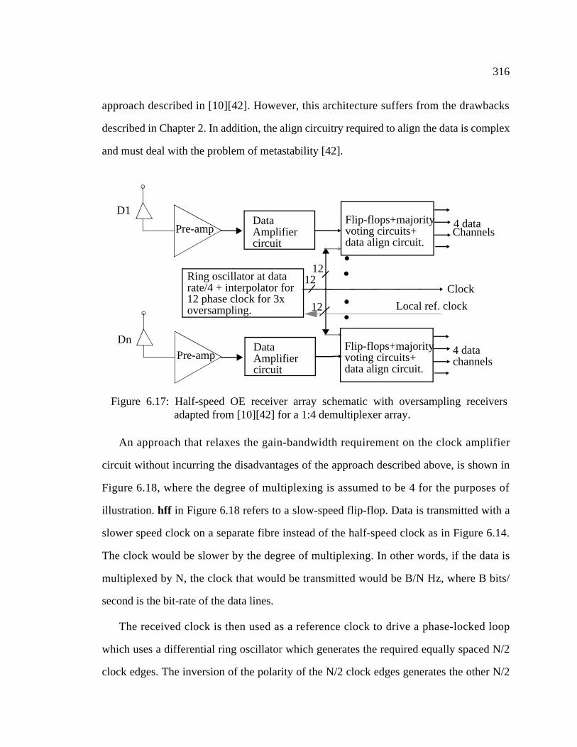
316
approach described in [10][42]. However, this architecture suffers from the drawbacks
described in Chapter 2. In addition, the align circuitry required to align the data is complex
and must deal with the problem of metastability [42].
An approach that relaxes the gain-bandwidth requirement on the clock amplifier
circuit without incurring the disadvantages of the approach described above, is shown in
Figure 6.18, where the degree of multiplexing is assumed to be 4 for the purposes of
illustration. hff in Figure 6.18 refers to a slow-speed flip-flop. Data is transmitted with a
slower speed clock on a separate fibre instead of the half-speed clock as in Figure 6.14.
The clock would be slower by the degree of multiplexing. In other words, if the data is
multiplexed by N, the clock that would be transmitted would be B/N Hz, where B bits/
second is the bit-rate of the data lines.
The received clock is then used as a reference clock to drive a phase-locked loop
which uses a differential ring oscillator which generates the required equally spaced N/2
clock edges. The inversion of the polarity of the N/2 clock edges generates the other N/2
DataAmplifiercircuit
DataAmplifiercircuit
4 dataChannels
D1
Dn
Figure 6.17: Half-speed OE receiver array schematic with oversampling receiversadapted from [10][42] for a 1:4 demultiplexer array.
Ring oscillator at data rate/4 + interpolator for12 phase clock for 3x oversampling.
Flip-flops+majorityvoting circuits+data align circuit.
12
12
12
4 dataFlip-flops+majorityvoting circuits+data align circuit.
channels
ClockLocal ref. clock
Pre-amp
Pre-amp

317
clock edges. Additionally, if N = 4, a ring oscillator would produce the quadrature clocks.
The generation of clocks by an oscillator guarantees that they are equally spaced because
of the nature of the ring oscillator. A differential oscillator also allows the use of an even
or odd number of delay stages for oscillation because of the option of using the phase
inverted negative output of a delay stage instead of the positive output.
The incoming clock is delayed so that data to be demultiplexed is sampled exactly
once in the middle of the bit. The disadvantage of this approach is that the clock jitter, and
the rise- and fall-times must meet the same requirements as for the case with the half-
speed clock. Additionally, the data has to be aligned after demultiplexing, with respect to a
clock edge out of the N-clock edges used. This has to be done in such a way that the clock
loading on all the clock edges is the same. This is difficult to ensure in practice due to the
uncertain intra- and inter -layer coupling capacitance data in a typical CMOS process
technology, which affects the accurate capacitance extraction from practical IC layouts.
Pre-amp
hff
hffhff
hff
DataAmplifiercircuit
DataAmplifiercircuit
Clock
4 dataChannels
Clk
D1
Dn
Figure 6.18: Half-speed OE receiver array schematic with synchronous receivers and aPLL in the clock channel, assuming the degree of demultiplexing to be 4and B to be bit rate of each data channel.
Low-jitter PLLrunning at B/4Hz.
4
4
align
phase
clock4
hff
hffhff
hff4 dataChannels
align
phase
clock
4
delay cell
Pre-amp
Pre-amp

318
An example of a phase-align circuit operation can be sketched as shown in Figure
6.19. The serial data waveform is represented as 1234abcd, where time increases from left
to right. 1 is therefore, the first bit that occurs in the serial-data stream (qin+) at the
receiver in one of the data channel amplifier circuit outputs in Figure 6.18. c1+, c1-, c2+
and c2- are the differential quadrature clock signal outputs of the PLL in Figure 6.18. q11,
q12, q13, and q14 correspond to the outputs of the first-level of hff circuits in each data
channel in Figure 6.18, which are produced by the latching action of c1+, c1-, c2+ and c2-
on the output of the data amplifier in each data channel. The phase-alignment
methodology in Figure 6.19 involves retiming q11 and q12 on the falling edge of c1+ to
give q21 and q22, and retimes q13 and q14 on the falling edge of c2- to give q23 and q24.
Retiming q21 and q22 on the falling edge of c1- gives q31 and q32 which can then be
retimed with q23 and q24 on the falling edge of c2+ to give a phase-aligned nibble at the
output of each data channel. The disadvantage here is that c2+ has an extra load of 2 flip-
flops compared to the other clocks. In fully differential operation, loading c2+ is
qin+c1+c2+
q11q12q13
q21q22
out3out2out1out0
1 2 3 4
Figure 6.19: Schematic of waveforms at the various nodes in phase-alignerexample in Figure 6.18.
c1-c2-
a b c d
12
34
12
34
12
1234
ab
cd
ab
cd
ab
abcd
retime on c1+
retime on c2-
retime on c1-
retime on c2+
q14
q23q24q31q32
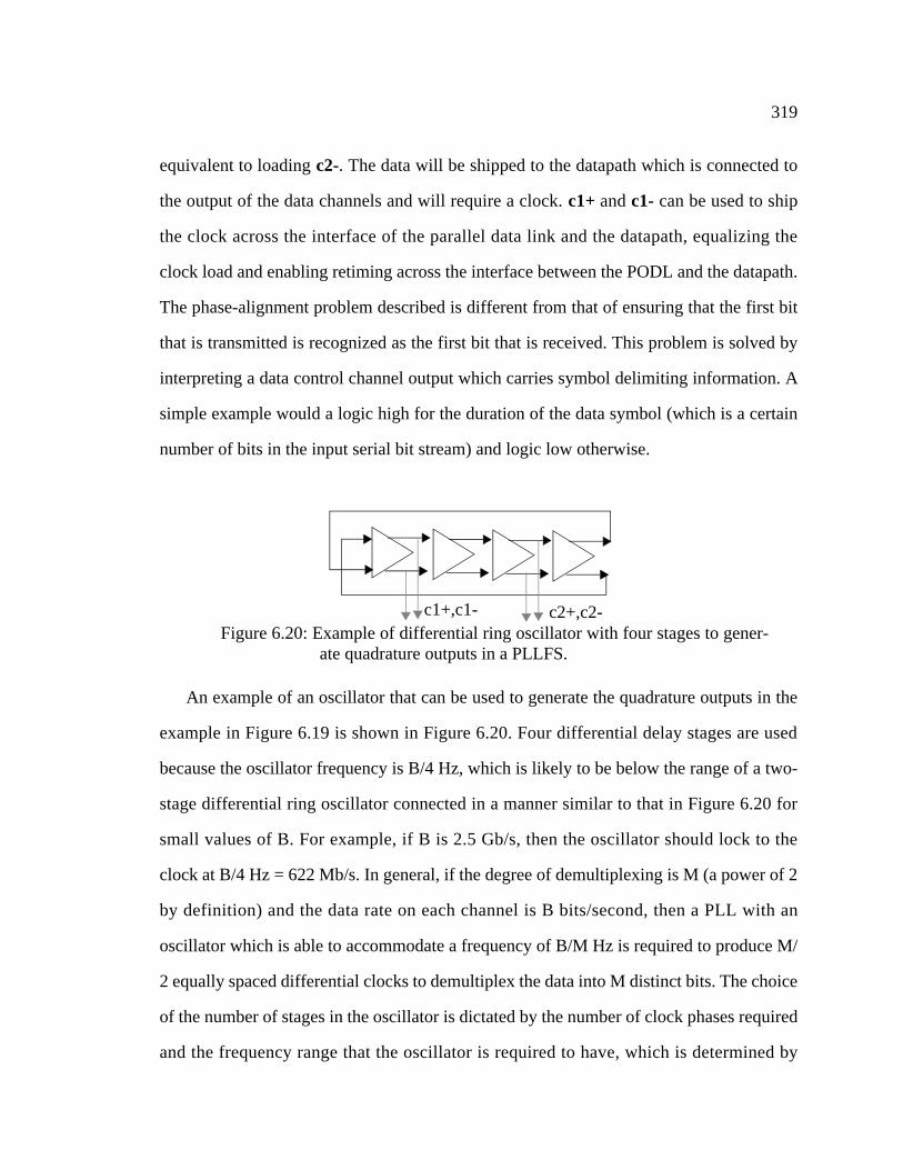
319
equivalent to loading c2-. The data will be shipped to the datapath which is connected to
the output of the data channels and will require a clock. c1+ and c1- can be used to ship
the clock across the interface of the parallel data link and the datapath, equalizing the
clock load and enabling retiming across the interface between the PODL and the datapath.
The phase-alignment problem described is different from that of ensuring that the first bit
that is transmitted is recognized as the first bit that is received. This problem is solved by
interpreting a data control channel output which carries symbol delimiting information. A
simple example would a logic high for the duration of the data symbol (which is a certain
number of bits in the input serial bit stream) and logic low otherwise.
An example of an oscillator that can be used to generate the quadrature outputs in the
example in Figure 6.19 is shown in Figure 6.20. Four differential delay stages are used
because the oscillator frequency is B/4 Hz, which is likely to be below the range of a two-
stage differential ring oscillator connected in a manner similar to that in Figure 6.20 for
small values of B. For example, if B is 2.5 Gb/s, then the oscillator should lock to the
clock at B/4 Hz = 622 Mb/s. In general, if the degree of demultiplexing is M (a power of 2
by definition) and the data rate on each channel is B bits/second, then a PLL with an
oscillator which is able to accommodate a frequency of B/M Hz is required to produce M/
2 equally spaced differential clocks to demultiplex the data into M distinct bits. The choice
of the number of stages in the oscillator is dictated by the number of clock phases required
and the frequency range that the oscillator is required to have, which is determined by
c1+,c1- c2+,c2-Figure 6.20: Example of differential ring oscillator with four stages to gener-
ate quadrature outputs in a PLLFS.

320
system-level design and test considerations, and the flexibility of application of the IC.
The delay-cell shown in Figure 6.14 and Figure 6.18 is needed to adjust the clock-to -data
setup time for the sampling flip-flops in the demultiplexer. This can be an open-loop or a
closed-loop process. A possible mechanism might be to transmit synchronization
sequences every so often as in [15][16], during which time a known data pattern is sent
over the data channels. The delay-adjustment circuitry adjusts the delay so that the delay is
in the middle of the super-imposed eye of all the known received bit pattern eye-diagrams.
6.3.1 TIA Design
Transimpedance amplifiers are the dominant type of OE pre-amplifiers used to
convert the received OE transducer current signal into a voltage signal, which can then be
subjected to further processing. Integrating receivers, which achieve sensitivities superior
to transimpedance amplifiers, have also been used. They integrate the input signal and
require some form of compensation or equalization (in the form of differentiating the
integrated signal), and therefore, suffer from poor dynamic range.
The factors that influence design of OE pre-amplifier arrays are
• The desired sensitivity, device noise mechanisms and channel-to-channel crosstalk.
• The desired data rate.
• The device technology that is to be used and the supply voltages that the technology
can tolerate, which determine the device transconductance and fT.
• The nature of the OE transducer -- its biasing requirements, whether it is available
in single-ended or differential form, whether it has isolated terminals or has a
common substrate among the elements of the array and whether the substrate is p-
or n-type.

321
• The desired number of channels in parallel and the area that is available to
accommodate them.
• The package, which determines the power-supply decoupling of the components of
each receiver channel and bond-wire isolation of channel power supplies.
• The available substrate noise reduction mechanisms.
• The complexity of the digital logic and the nature of the logic style that is used to
implement digital functionality, if any, on the same IC.
The fastest OE pre-amplifier reported in CMOS so far has a measured7 data rate of
1.25 Gb/s at -10 dBm sensitivity (100 µA input current) and BER < 3.3 x 10⁻¹⁰ for -23
dBm (electrical) sensitivity for 1.25 Gb/s input data patterns [26]. The power consumed
by this circuit is 78 mW from a 3.3 V power supply. There have been no CMOS OE pre-
amplifier or receiver arrays reported in the literature to date. The design of these receiver
arrays have to trade-off receiver sensitivity, power consumption, data rate and OE
transducer parasitic capacitance. Receiver sensitivity is affected by the considerations of
eye-safety and link-loss as characterized by the LTF.
Preliminary calculations from a simplified FET noise model indicate that for a 0.5 µm
CMOS technology, the power-supply consumption of the Common-Gate (CG) Front-End
(FE) of a single-stage CG Common-Source (CS) Shunt-Shunt (SS) amplifier would be
approximately 1 mW at -10 dBm input sensitivity, and approximately 100 mW at -20 dBm
sensitivity, to achieve a stage bandwidth of 3.5 GHz and a transimpedance of 1000 Ohms
(Figure 6.38). A per-stage bandwidth of 3.5 GHz is needed because a three-stage amplifier
which can accommodate 2.5 Gb/s requires individual stages with -3 dB bandwidth of
1.414*Bitrate Hz (Equation 6.64). The performance achieved in practice is in all
7. Electrical test with 320 fF capacitor mocking up photodiode capacitance.

322
likelihood to be worse than these predicted values because of the simplified nature of the
calculations.
Traditionally, OE receivers have been designed with OE pre-amplifiers, AGC circuits,
automatic offset-control (AOC) circuits, amplifiers and decision circuits. AGCs are used
to obtain high gain and low noise by increasing the feedback resistance of the pre-
amplifier for low input-currents while reducing the feedback resistance for large input-
currents. AGCs are also required if the receiver decision-circuit saturates or has ISI-effects
due to the large input currents as opposed to small input-currents from the OE transducer.
An AOC circuit is required if the input signal light levels fluctuate. In other words, if the
light level corresponding to logic low varies over time, it causes the bias points of the
amplifier to change, affecting the performance of the circuit, even causing it to
malfunction. This effect would be especially troublesome on the clock receiver in a
parallel data-link. In this work, we assume that the optical modulation is strictly on-off
modulation at the laser-diode end, and that the laser-diode is below threshold by a
sufficient margin such that the logic-low light-level is negligible and constant for all
practical considerations.
Since CMOS technology is a non-saturating technology due to the unipolar majority
carrier nature of the devices, we adopt a design philosophy of amplifying the input current
signal from the OE transducer using the minimum number of stages, and converting it to a
differential signal, using a method similar to [26] or [122]. The OE pre-amplifier is
designed to amplify the smallest expected input signal to an amplitude that is sufficient for
the data retiming flip-flops in the data channels and for the clock amplifier (Figure 6.14)
or the PLL in the clock receiver channel (Figure 6.18). The pre-amplifier architecture and
current levels are chosen so that variations in the input current level do not affect the bias
points of the circuit, causing the downstream DC-coupled amplifiers to move away from

323
their bias points. The retiming flip-flops are designed such that they do not saturate. Under
these assumptions, we do not use an AGC as part of our optical receiver.
For high-speed low-power applications, especially in parallel optical data-links where
the receiver circuits are integrated with complex digital circuits on the same substrate, it is
extremely advantageous to operate with large light levels and low input OE transducer
capacitance. The large Signal-to-Noise Ratio (SNR) will enable the minimum number8 of
DC-coupled amplifiers in each receiver channel required to achieve the minimum signal
amplitude to retime a signal, which in turn will reduce the impact of bias-point variations
due to signal and process variations, as well as the impact of power-supply and substrate
noise, because of high SNR. The power consumption is also reduced while increasing the
maximum sustainable data rate.
Accordingly, the block diagram of the optical receiver that is to be designed for the
parallel optical data-link is shown in Figure 6.21. The OE pre-amplifier (“Pre-amp” in
Figure 6.21) consists of the minimum number of stages required to produce a differential
8. The low transconductance of CMOS devices means that individual stage gainsare likely to be low compared to Si-Bipolar, GaAs MESFETS or other advancedtechnologies. This implies that more stages are required to achieve a certainbandwidth than would be needed in other technologies, lowering the achievablebandwidth.
Pre-amp
hff
hffhff
hff
Amplifiercircuit
4 dataChannels
Clk
Din
Figure 6.21: Half-speed optical receiver schematic with synchronousreceiver, assuming degree of demultiplexing to be 4.
align
phase
clock

324
signal, which is amplified by the amplifier circuit to drive the flip-flops hff, whose
number is determined by the degree of multiplexing/demultiplexing in each data line.
These retiming flip-flops are designed so that they present the minimum amount of
capacitance to the data and clock inputs so that the gain-bandwidth requirements on the
amplifier circuits are reduced. Strategies described earlier can be used to address the gain-
bandwidth trade-offs associated with the choice of the clock-receiver architecture.
6.3.2 CMOS OE Receiver Analysis
6.3.2.1 MOSFET Noise Model
MOSFET noise is discussed extensively in the literature. A good reference for
MOSFET noise is [183]. Second-order MOS noise sources in sub-micron MOSFETs have
been discussed in [184], [185], [186], [187], [188] and [189]. The noise contribution of the
distributed gate resistance is neglected here because of the low resistance of salicided
polysilicon (2 ohms/square) and the interleaved-layout style for large transistors. The
distributed substrate resistance (thermal) noise is minimum when the substrate bias is
greater than 2.0 V [188]. This, however, is not the situation in most CMOS ICs. For all
practical purposes, the substrate thermal-noise can be approximated by considering the
substrate resistance and then adding the thermal noise of this resistor to the MOSFET
thermal noise. Flicker noise is neglected here because its contribution is negligible
compared to the noise contribution of other device noise-current sources in high bit rate
OE receiver design. The drain noise-current Power Spectral Density (PSD) is given by
(6.9)
where gd0 is the zero bias drain-to-source conductance and γ is a bias-dependent factor
which is typically between 0.67 and 1 for long-channel devices. In saturation, the value of
fdd Id Id∗⋅⟨ ⟩ 4kTγgd0=

325
γ is closer to 0.67, while it is closer to 1 when the drain-to-source voltage is close to zero.
In short-channel devices, due to hot-electron effects in the MOSFET channel, the value of
γ is much higher than 0.67 in saturation.
If we define αsat as gm/gd0, where γ corresponds to its saturation value (0.67), we get
(6.10)
where Γ = γ/αsat, is defined as the excess channel thermal-noise.
This relationship is useful because the device transconductance is the variable that is
manipulated during circuit analysis and design. Figure 6.10 offers direct insight into how
the device noise changes with changes in the transconductance. We will use this
relationship in our noise analysis involving MOSFET devices. αsat is typically 1 for
saturation in long-channel devices, and tends to 0.5 and below, for saturation in short-
channel devices. αsat is simulated to have values between 0.4 and 0.5 for the 0.5 µm
CMOS process technology, between 0.3 and 0.4 for a typical 0.35 µm CMOS process
technology and between 0.25 and 0.3 for a 0.18 µm CMOS process technology. For long
CgsIg
Vgs
Vds
gdsIdgmVgs
Cgs
Vgs+-
Erig
Figure 6.22: MOSFET noise model [183], showing noise sources considered in thiswork.
rg
gg
Vds
gdsIdgmVgs
fdd Id Id∗⋅⟨ ⟩ 4kTgm
γgd0
gm---------- 4kTΓgm= =

326
channel MOSFETs in saturation, αsat tends to 1 and γ is ~0.67, giving a value of ~0.67 for
Γ. For short channel devices, however, γ increases from 0.67 to ~1.2 for 0.5 µm CMOS
technology and to higher values for finer feature size CMOS process technologies. This
gives a value of ~2.4 for Γ for the 0.5 µm CMOS process technology.
At high frequencies, the distributed nature of the gate of the MOSFET device causes a
phase-shift of the gate impedance from the purely capacitive behavior at low frequencies.
This shift can be modeled by a real, noiseless conductance in parallel with the gate. The
shunt noise-current source, Ig, represents the induced gate noise-current associated with
the noiseless conductance in parallel with the gate of the MOSFET. The equivalent small-
signal noise model of the MOSFET is shown in Figure 6.22. The induced gate noise-
current PSD is
(6.11)
The gate-drain noise-current cross-spectral power-density is given by
(6.12)
where c is the correlation coefficient of the induced gate noise-current with the drain cur-
rent.
The value of c is between 0.3 and 0.4 for a constant-mobility MOSFET model, and
increases in magnitude to between 0.8 and 0.9 for velocity saturated MOSFET devices
[190][184]. The sign of c depends on the way the cross-correlation has been written. For
the equivalent noise-voltage model for gate noise shown in Figure 6.22,
(6.13)
fdd Ig Ig∗⋅⟨ ⟩
4kTδ ωCgs( )2
5gd0---------------------------------=
fdd Ig Id∗⋅⟨ ⟩ jc
4kTδ ωCgs( )2
5gd0--------------------------------- 4kTΓgm j
c4kTω2Cgs2
gm---------------------------- δγ
5-----= =
fdd Eri Eri∗⋅⟨ ⟩ 4kTδrg=

327
and the gate-drain noise cross-spectral PSD is given by
(6.14)
The gate-oxide thickness in modern advanced CMOS process technologies is
shrinking dramatically. The 0.5 µm CMOS that we use in this work has a typical gate-
oxide thickness of 90 nm, which decreases to 30 nm for a 0.1 µm CMOS process [2]. This
causes a gate-leakage current due to tunnelling and/or surface leakage, that is strongly
temperature-dependent. The gate-leakage current is typically 1 nA/µm for NMOS
transistors in a 0.1 µm CMOS process [2]. The gate-leakage noise-current PSD could
easily approach that of a PIN photodiode for NMOS MOSFETs whose minimum feature
size is 0.5 µm or less. The noise-current PSD is that of a shot-noise process and is given by
2qIg, where Ig is the mean gate current. The gate-leakage noise-current contribution is
negligible compared to the noise contribution from other sources in high bit-rate OE
receivers.
The series resistances associated with the device terminals also add thermal noise of
4kBTR, where R is the resistance. In this process, the diffusions are salicided for low
resistance. This diffusion and polysilicon contact resistance is likely to dominate the
terminal resistance. This can be made negligible by using multiple contacts, which is the
norm in any case, as the devices tend to be large. In the noise analysis that we perform, the
series-resistance noise terms will be neglected. substrate thermal-noise is assumed to be
negligible because of a large number of substrate contacts close to the device in layout.
The analysis in this section will initially neglect the correlated induced gate-noise for the
sake of simplicity and then modify the results to factor in induced gate-noise
considerations. Our goal is to gain insight into the trade-off between the parameters of
power consumption, sensitivity and bandwidth in OE receiver design.
fdd Eri Id∗⋅⟨ ⟩ jc 4kTδrg 4kTΓgm=

328
6.3.2.2 Noise Analysis Techniques
We use a technique called the method of transposition of sources for noise analysis
[184][190]. A brief summary of the basic transformations is shown in Figure 6.23 (a)-(f).
Figure 6.23 (a) and (b) are the familiar rules from electrical circuit theory for composition
of voltage and current sources. Figure 6.23 (c) is the familiar Thevenin-Norton
transformation technique. Figure 6.23 (d) is a transformation called “pushing a voltage
through a node” -- in this case node b. This transformation fulfills KVL in the loop
consisting of nodes dcbd, dcabd and cabc.
Figure 6.23 (e) is called “pushing a current through a branch” -- in this case branch bc.
The current flowing into node c from branch bc can be viewed as due to the same current
flowing through branch ba, br, and ac. The final transformation is called pushing a
voltage through a transconductance. This is obtained from the rearrangement of Equation
6.15 to Equation 6.16.
(6.15)
(6.16)
This technique allows the transposition of a current source/sink at the output of a two-
port network across a transconductance into a voltage at the input. Similarly, the same
technique can be applied to the transposition of a voltage source/sink at the output of a
two-port network across a transresistance.
gmVbs gmVas In+=
Vbs VasIn
gm------+=

329
+- +
-
+-
+-
+-
+-d
c
ba a b
c
d
a c
b
a c
b
+-a
s
b d
s
IngmVas
a b
s
d
s
gmVbsIn/gm
+-
R
V V/R R
(a) R1 (b) R2
(c) R3: Thevenin-Norton
(d) R4: pushing a voltage through a node (node b)
(e) R5: Pushing a current through across a branch (branch bc)
(f) R6: Pushing a voltage through a transconductance
Figure 6.23: Rules R1 through R6 for the transposition of sources method ofdetermining input-referred noise-current PSD of a linear two-port network.
T <-> N

330
We look at two examples to illustrate the process of applying the above rules to
determine the input-referred noise-current/voltage PSD. Figure 6.25 shows the block
diagram and AC-schematic of an elementary TIA. Figure 6.26 shows the noise sources
associated with the small-signal model diagram in Figure 6.25.
Since this is a TIA, we try to determine the input-referred noise-current PSD
Accordingly, the noise sources are cast as noise-current sources. I1, the noise-current PSD
of Rf is equal to 4kBT/Rf. I2, the combined noise-current PSD of the transistor and RL, is
equal to 4kBTΓgm + 4kBT/RL. There are assumed to be no other noise sources. The
photodiode has a noise-current PSD Isig = 2qId, where Id is the dark current of the
photodiode.
+-+-R1
R2
R3
Vn R1
R2
R3
(R1+R2)Vn/R3
Figure 6.24: Rule R7: pushing a voltage through a resistive divider.
R1
R2
R3Vn/R3
T->N N -> T
Rf
Av
Isig
+-
Rf
A2VdRL
gmVgs
Vgs
Vd=-gmRLVgs
Isig
Figure 6.25: Elementary TIA and its equivalent small-signal model.

331
+-
+-
+-gmVg
Vg
RLI2/gm
Rf
Rf
I1
AvVd
Vd
RLI2gmVg
CTIsig
IsigI1
I1CT
Figure 6.26: Transformation of small-signal model by transposition of noisesources I1 and I2 from the output to the input. The transposednoise-current source I1 in parallel with a voltage source is
R5, R6
+-
+-
+-
+-
AvVg
VggmVg
gmVgIsig
Isig
RL
Rf
Rf
CTI1
I1 RL
I2/gm
I2/gm
Vg
I2/gmRf
I2(jωCT/gm)
AvVg
Figure 6.27: Small-signal model after transposition of I2/gm in Figure 6.26
R4
R3,R4,R2
(a)
(b)
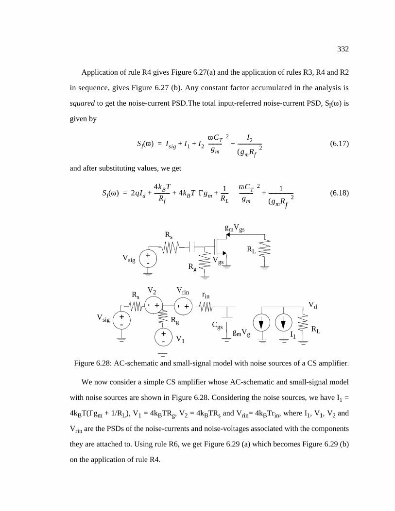
332
Application of rule R4 gives Figure 6.27(a) and the application of rules R3, R4 and R2
in sequence, gives Figure 6.27 (b). Any constant factor accumulated in the analysis is
squared to get the noise-current PSD.The total input-referred noise-current PSD, SI(ω) is
given by
(6.17)
and after substituting values, we get
(6.18)
We now consider a simple CS amplifier whose AC-schematic and small-signal model
with noise sources are shown in Figure 6.28. Considering the noise sources, we have I1 =
4kBT(Γgm + 1/RL), V1 = 4kBTRg, V2 = 4kBTRs and Vrin= 4kBTrin, where I1, V1, V2 and
Vrin are the PSDs of the noise-currents and noise-voltages associated with the components
they are attached to. Using rule R6, we get Figure 6.29 (a) which becomes Figure 6.29 (b)
on the application of rule R4.
SI ω( ) Isig I1 I2ωCT
gm-----------
2 I2
gmRf( )2-------------------+ + +=
SI ω( ) 2qId4kBT
Rf------------ 4kBT Γgm
1RL------+
ωCT
gm-----------
2 1
gmRf( )2-------------------+
+ +=
RL
gmVgs
VgsVsig
+- Rg
Rs
Vd
RLI1gmVg
CgsVsig
+-
+-
+-
+-
rinVrin
V1
V2Rs
Rg
Figure 6.28: AC-schematic and small-signal model with noise sources of a CS amplifier.

333
Vd
RLgmVgCgs
Vsig
+-
+-
+-
+-
rinVrin
V1
V2Rs
Rg
+-
Vg
I1/gm
Vd
RLgmVg
Cgs
Vsig
+-
+-
+-
+-
rinVrin
V1
V2Rs
Rg
+- Vg
I1/gm
+-I1/gm
Figure 6.29: Transposition of I1 in Figure 6.28 to the input.
(a)
(b)
R4
Vd
RLgmVgCgs
Vsig
+-
+-
+-
+-
rinVrin
V1
V2Rs
Rg
+- Vg
I1/gm I1/gm((rin+(Rs||Rg))jωCgs)
+-
Vsig
+-
+-
V1
Rs Rg Vsig +-
Rs Rg
+-
V1Rs/Rg
Vsig
+- V3
Rs
Rg
+-
Vsig
+-
Rs
Rg
+-
+-
V3
V3
Vsig+-
Rs
Rg
+-
V3(1+Rs/Rg)
Figure 6.30: Transposition of all noise sources to the input.
R3
R7
R4
R7

334
Applying rules R3, R7, R4 and R7, we move from Figure 6.29 (b) to Figure 6.30 and
then to Figure 6.31, where we see all the input-referred noise-voltage PSDs.
(6.19)
(6.20)
(6.21)
(6.22)
(6.23)
Considering induced gate noise-current effects in the above analysis, we note that
since the conductance gg in Figure 6.22 is a real, noiseless conductance, the
transformation rules that we discussed so far (rules R1 through R7) do not apply in the
movement of noise-current and noise-voltage sources across it. This maintains
consistency with the traditional noise analysis approach. Therefore, in order to avoid
confusion, we do not draw gg in the noise-source transposition diagrams. Note that every
V2 4kBTRs=
V1 4kBTRg=
Vrin 4kBTrin=
I1 4kBTΓgm4kBT
RL------------+=
Vd
RLgmVg
CgsVsig
+-+- +-+-
rinVrin(1+Rs/Rg)
V1Rs/Rg V2 Rs
Rg
Vg
I1(1+Rs/Rg)*1/gm*(1+(rin+(Rs||Rg))jωCgs)+-
Figure 6.31: Final small-signal model of the CS amplifier showing all noise sourcesreferred to the input.
Svneq ω( )4kBT
-------------------- Rs Ri 1Rs
Rg------+
2
Rg
RsRg------
2
Γgm1
RL------+
1gm------ 1
Rs
Rg------+
2
1 ωCgs( )2 1 Rs Rg||+( )2+( )
+ +
+
=

335
transistor now contributes its induced gate noise-current PSD and its correlated gate-drain
noise-current PSD to the input-referred noise-current PSD, in addition to its input-referred
drain noise-current PSD. Also note that the induced gate noise-current PSD of each
transistor is correlated only to its input-referred drain noise-current PSD and not to that of
any other transistor. Given that the input-referred drain noise-current PSD of a simple CS
amplifier is equal to 4kBTΓω2Cgs2/gm, the excess noise contribution can be quantified as
(6.24)
The first term in Equation 6.26 corresponds to the input-referred drain noise-current
PSD, the second term to the induced gate noise-current PSD and the third term to the
drain-gate noise-current cross-spectral power density.
(6.25)
Assuming that the relationship δ = 2γ, which holds for long-channel MOSFETs, holds
for short-channel MOSFETs,
(6.26)
Therefore, we see that the induced gate noise-current can be included in the noise
analysis by multiplying the input-referred drain noise-current PSD by the right-hand side
of Equation 6.26. Taking, for example, typical 0.5 mm CMOS process technology values,
we get the multiplication factor corresponding to the induced gate noise-current for the
case of a CS amplifier as (1 + 0.1 + 0.24) = 1.34. In other words, there is a 34% increase in
the input-referred noise-current PSD. Note that we have assumed that the correlation
coefficient c, for the drain-gate cross-spectral power density is ~0.4 for the 0.5 µm CMOS
process technology.
SCS ω( )4kBTΓω2Cgs
2
gm--------------------------------
4kTδω2Cgs2
5gd0---------------------------- 2c
4kBTΓω2Cgs2
gm--------------------------------
4kTδω2Cgs2
5gd0----------------------------+ +=
SCS ω( )4kBTΓω2Cgs
2
gm-------------------------------- 1
δgm
5Γgd0--------------- 2c
δgm
5Γgd0---------------+ +
=
SCS ω( )gm
4kBTΓω2Cgs2
-------------------------------- 1 2α2
5--------- 2cα 2
5---+ +
=

336
Following a similar analysis for the case of the CG FE transistor in a CG OE receiver,
we note that the same results as the above hold. That is, the input-referred drain noise-
current PSD of the CG transistor in the CG OE receiver is multiplied by the right-hand
side of Equation 6.26 to account for the induced gate-noise in the noise analysis.
Accordingly, we proceed in our noise calculations without explicitly taking the induced
gate-noise into account. We then multiply the input-referred noise-current PSD of the
input transistor (CG or CS) by the right-hand side of Equation 6.26 to account for the
induced gate-noise.
6.3.2.3 Receiver SNR Calculation
The photo-diode current, Iph, generated by a PIN diode with quantum efficiency, η, for
emission frequency, ν, at the received optical power, Popt, is given by [41]
(6.27)
This current appears at the output of a transimpedance amplifier (whose transfer
function, ZT(ω)) as a voltage Vo given by
(6.28)
where K is chosen so that ZT(ω->0) --> 1.
If the input noise-current PSD of the transimpedance amplifier is assumed to be9
(6.29)
9. This is the representative form of the input-referred noise-current PSD for FETCS and CG transimpedance amplifiers.
Iphqhv------ηP
opt=
VO KZT ω( )Iph=
SI f( ) a bf2+=

337
The output signal has variance
(6.30)
The output signal has magnitude10 (choosing K so that ZT(ω=0) is 1)
(6.31)
Assuming Gaussian statistics on the noise at the input of the decision circuit and ISI-
free input data, the probability of making the error of identifying a logic low (“0”) bit as a
logic high (“1”) bit, P(E10), is given by 0.5 erfc(Q/1.414) [41]. The SNR, Q = (D-s(j))/σj,
where D is the detected signal, s(j) is the signal value corresponding to logic j (j = 0 (logic
low) or 1 (logic high)) and σj is the rms noise [64]. When on-off laser modulation is used,
s(0) = 0 at the PIN diode. The probability of a logic low to logic high error is as likely as
that of a logic high to logic low error in a random bit stream, as bits with logic high and
logic low values occur with equal probability. The SNR, Q, is then the ratio of average
decision-circuit input-voltage (one-half of the peak voltage) to the rms input-noise, σvn.
(6.32)
P(Error) = 10-9 implies that IinZT(0)/2X = Q = 6. Solving for Iin, we get
(6.33)
In general,
(6.34)
10. Under ISI-free assumption.
σvn2 K2 ZT f( ) 2 a bf2+( ) fd
0
∞
∫ KX( )2= =
Vout KIinZT ω 0=( )=
QKIinZT 0( )
2KX-----------------------
IinZT 0( )2X
-------------------= =
Iin2XQZT 0( )------------- 2Q ZT f( )
ZT 0( )-------------
2a bf2+( ) fd
0
∞
∫= =
Iin 2Q ZT f( )ZT 0( )-------------
2SI f( ) fd
0
∞
∫=

338
6.3.2.4 Receiver Sensitivity Assuming Gaussian Statistics
The optical power, Popt, corresponding to the received logic high value, is P1. This
implies that , where q is the charge of an electron, equal to 1.6 x10⁻¹⁹
Coulombs. The optical power, Popt, corresponding to the received logic low value, is P0,
implying that . The average power is given by 0.5 P1 = .
The minimum optical power required for the desired BER is
(6.35)
The mean-square noise-current is
(6.36)
where the input noise-current PSD is
(6.37)
The transimpedance ZT(f), when the feedback resistor, Rf, is chosen to make the
transfer function Maximally Flat Magnitude (MFM) for an amplifier with a single pole at
f-3, is given by Equation 6.38.
(6.38)
Writing , Equation 6.36 becomes (6.39)
(6.40)
Iinηqhυ------P1=
Iin 0= 0.5Iinhυηq------
Pminhυηq------Q ZT f( )
ZT 0( )-------------
2SI f( ) fd
0
∞
∫=
In2⟨ ⟩ ZT f( )
ZT 0( )-------------
2SI f( ) fd
0
∞
∫=
SI f( ) a bf2+=
ZT f( )ZT 0( )
1 jf0.5f 3– 1 j+( )------------------------------+
1 jf0.5f 3– 1 j–( )------------------------------+
------------------------------------------------------------------------------------------=
y f f 3–⁄=
In2⟨ ⟩ f 3–
ZT yf 3–( )ZT 0( )
-------------------2SI yf 3–( ) yd
0
∞
∫=

339
(6.41)
(6.42)
(6.43)
where I2 and I3 are called the second and third Personick integrals respectively. I2 can be
evaluated numerically for the ZT(f) in Equation 6.38 [41] as
(6.44)
I3 can be evaluated numerically for the ZT(f) in Equation 6.38 as
(6.45)
The minimum received optical power for the desired SNR at the receiver becomes
(6.46)
6.3.2.5 Optimal Noise Design of OE Receivers
Consider the Common-Gate TransImpedance Amplifier (CGTIA) shown in Figure
6.32. Cd is the OE transducer capacitance (that of a PIN diode in this case), Cgs1 is the
gate-to-source capacitance of M1, Cgs2 is the gate-to-source capacitance of M2 and Cgd1 is
the gate-to-source capacitance of M2. The input-referred noise-current PSD of M1 is
In2⟨ ⟩ f 3–
ZT yf 3–( )ZT 0( )
-------------------2
a by2f 3–2+( ) yd
0
∞
∫=
In2⟨ ⟩ af 3–
ZT yf 3–( )ZT 0( )
-------------------2
yd0
∞
∫ bf 3–3 ZT yf 3–( )
ZT 0( )-------------------
2y2 yd
0
∞
∫+=
In2⟨ ⟩ af 3– I2 bf 3–
3 I3+=
I2ZT yf 3–( )
ZT 0( )-------------------
2yd
0
∞
∫ 0.7854= =
I3ZT yf 3–( )
ZT 0( )-------------------
2y2 yd
0
∞
∫ 0.393= =
Pminhυηq------Q Iin
2⟨ ⟩ hυηq------Q af 3– I2 bf 3–
3 I3+= =

340
(6.47)
Assuming that ωT = gm/Cgs, where ωT is the unity gain frequency of M1 in rad/s, Equation
6.47 becomes
(6.48)
Equation 6.48 is minimized if Cgs1 = Cd. This gives
(6.49)
(6.50)
where we have assumed that Cgs2 > Cgd1, and substituted for ωT in Equation 6.49. Taking
the ratio of the noise-current PSDs of the contributions of M1 and M2, we get
SIM1 f( )4kBTΓ
gm1---------------- 2πf( )2 Cgs1 Cd+( )2=
SIM1 f( )4kBTΓ
2πfT1Cgs1------------------------- 2πf( )2 Cgs1 Cd+( )2 4kBTΓ
fT----------------2πf2 Cgs1 Cd+( )2
Cgs1-------------------------------= =
Rf
-AvM2
M1
Cgs2+Cgd1Cgs1+Cd
A B
Figure 6.32: AC-schematic of CG OE pre-amplifier.
SIM1 f( )4kBTΓ
fT1----------------8πf2Cd
32πkBTΓf2
fT1---------------------------Cd= =
SIM2 f( )4kBTΓ
gm2---------------- 2πf2( ) Cgs2 Cgd1+( )2 4kBTΓ
fT2----------------2πf2 Cgs2 Cgd1+( )2
Cgs2------------------------------------
8πkBTΓf2
fT2------------------------Cgs2
= =
=

341
(6.51)
where Cgs2/Cd = Cgs2/Cgs1 = W2LdCov/W1LdCov, where Ld is the gate overlap of diffu-
sion and Cov is the gate-diffusion overlap capacitance per unit width in F/m. Assuming
that M1 and M2 have the same gate overdrive,
(6.52)
For negligible noise contribution from M2, we set W2 << W1, determined by the
transconductance gm2 required for the gain of the second stage. If W2 = W1/2, the noise
contribution of M2 is 1/8 the noise contribution of M1. The pole fpA, at node A in Figure
6.32 is
(6.53)
The pole fpB at node B in Figure 6.32 is
(6.54)
6.3.2.6 Power Supply Consumption of Noise-Optimal OE Receivers
Neglecting the photodiode leakage and the gate-leakage current noise contribution to
the input-referred noise-current PSD of the CGTIA in Figure 6.33, the total input-referred
noise-current PSD is given by Equation 6.55.
(6.55)
SIM2 f( )SIM1 f( )---------------- 1
4---
Cgs2
Cd-----------
fT1
fT2------
14---
Cgs2
Cd-----------
2 gm1
gm1--------
= =
SIM2 f( )SIM2 f( )---------------- 1
4---
W2
W1-------
=
fpAgm1
2π Cgs1 Cd+( )-----------------------------------
gm1
2π2Cgs1---------------------
fT1
2------= = =
fpB1 Av+( )
2πRf Cgs2 Cgd1+( )----------------------------------------------=
SI f( ) 4kBT 1Rf----- 1
Rd1--------+
4kBTΓ
gm1---------------- 1
Rf2
------ 1
Rd12
-------- 2πf( )2 Cd Cgs1+( )2+ +
4kBTΓgm2
---------------- 1
Rf2
------ 1
Rd12
-------- 2πf( )2 Cgd1
Cgd2 Cgs2+ +( )2+ +
+
+
=
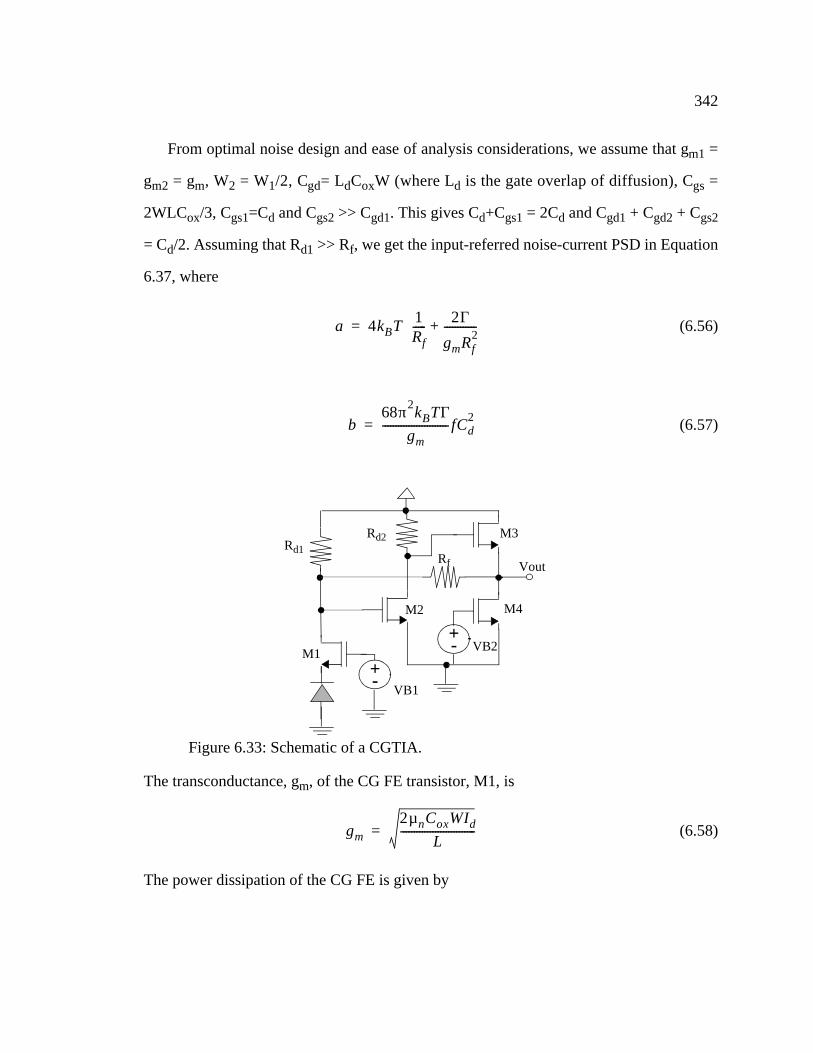
342
From optimal noise design and ease of analysis considerations, we assume that gm1 =
gm2 = gm, W2 = W1/2, Cgd= LdCoxW (where Ld is the gate overlap of diffusion), Cgs =
2WLCox/3, Cgs1=Cd and Cgs2 >> Cgd1. This gives Cd+Cgs1 = 2Cd and Cgd1 + Cgd2 + Cgs2
= Cd/2. Assuming that Rd1 >> Rf, we get the input-referred noise-current PSD in Equation
6.37, where
(6.56)
(6.57)
The transconductance, gm, of the CG FE transistor, M1, is
(6.58)
The power dissipation of the CG FE is given by
a 4kBT 1Rf----- 2Γ
gmRf2
------------+
=
b68π2kBTΓ
gm------------------------- fCd
2=
+-
Rf
Rd1Rd2
M1
M2
M3
M4
VB1
+- VB2
Vout
Figure 6.33: Schematic of a CGTIA.
gm2µnCoxWId
L----------------------------=

343
(6.59)
The minimum received optical power, , for the desired SNR, Q, is given by
(6.60)
Rearranging terms,
(6.61)
Substituting values in Equation 6.37 at T = 300 °K,
(6.62)
Equating Equation 6.37 and Equation 6.61,
(6.63)
(6.64)
(6.65)
Substituting values in Equation 6.61, we get
Ps Vddgm
2 L2µnCoxW-----------------------⋅=
Pmin
Pminhυηq------Q Iin
2⟨ ⟩ hυηq------Q af 3– I2 bf 3–
3 I3+= =
Iin2⟨ ⟩ Pmin
0.805ηλQ
--------------------- 2
0.65 PminηλQ-------
2= =
In2⟨ ⟩ af 3– I2 bf 3–
3 I3+ 0.7854af 3– 0.2678bf 3–3+= =
4kBT 1Rf----- 2Γ
gmRf2
------------+
f 3– I268π2kBTΓ
gm-------------------------Cd
2f 3–2 I3+ 0.65 Pmin
ηλQ-------
2=
8kBTΓgm
----------------I2
Rf2
------f 3– 8.5π2I3Cd2f 3–
3+
0.65 PminηλQ-------
2 4kBTI2f 3–
Rf------------------------–=
gm
8kBTΓI2f 3–
Rf2
----------- 8.5π2Cd2 f 3–
3 I3+
0.65 PminηλQ-------
2 4kBTI2f 3–
Rf------------------------–
------------------------------------------------------------------------=

344
(6.66)
Optimal noise design means that Cd = Cgs = 2WLCox/3 which implies that Cox = 3Cd/
2WL. The power dissipation of the CG FE becomes
(6.67)
Substituting Equation 6.66 in Equation 6.67,
(6.68)
From Equation 6.68, we see that Ps, the power consumption of the CG FE of the OE
receiver, is proportional to the third power of Cd. For a given CMOS process technology,
the variables that we can manipulate to achieve low Ps are Γ, λ, Rf, Cd, and Pmin. We can
reduce Γ to the lowest achievable value by using the minimum gate overdrive, use the
highest Rf, the lowest Cd, and the largest optical-power that the system can deliver, to
achieve operation at the desired bit rate. Some of these variables are influenced more
strongly by system-level design considerations, such as ease and cost of fabrication, and
eye-safety considerations. These considerations for OE receiver modules with 50 µm or
62.5 µm core diameter multi-mode fiber dictate the use of passive alignment techniques
with low coupling-loss, which favor the use of large diameter photodiodes (with the
attendant large parasitic photodiode capacitance). Similarly, eye-safety considerations
limit the amount of optical power that can be launched into the fiber by lasers at the
transmission end, reducing the amount of optical power available at the receive side. Both
gm
3.3 10 20–× Γ0.7854f 3–
Rf2
----------------------- 32.97Cd2f 3–
3+
0.65 PminηλQ-------
2 1.3 10 20–× f 3–
Rf---------------------------------–
---------------------------------------------------------------------------------------------=
PS Vddgm
2 L2µnCoxW-----------------------⋅ Vdd
gm2 L2
3µnCd----------------⋅= =
PsVddL2
3µnCd----------------
8kBTΓI2f 3–
Rf2
----------- I38.5π2Cd2f 3–
3+
0.65 PminηλQ-------
2 4kBTI2f 3–
Rf------------------------–
------------------------------------------------------------------------
2
=

345
of these considerations drive up the power consumption of OE receivers in CMOS process
technology, compared to the power consumption if these considerations were relaxed. It is
also desirable to move the wavelength of laser emission, λ, towards 1.3 µm as opposed to
850 nm, because dispersion and attenuation in the fiber lower at λ = 1.3 µm. It is however,
harder to make VCSELs at longer wavelengths because the quality factor of the VCSEL
cavity decreases with increasing wavelength, requiring increased mirror reflectivity.
The key variables and some typical values of Equation 6.68 are summarized below:
• Cd is the photodiode and pad capacitance
• Γ is the excess channel thermal-noise factor (1.5, can be as high as 4).
• λ is the emission wavelength in µm (0.85 µm)
• η is the quantum efficiency of photodiode (0.8)
• Q is the SNR for desired BER. (6 for BER<10-9, 7.35 for BER < 10-13).
• Rf is the transimpedance of the receiver front-end
• f-3 is the stage bandwidth of each amplifier used in the amplifier chain
• L is the effective channel length of the transistors used in the front-end
• is the minimum average received optical power for logic high
• kB is the Boltzmann’s constant
• T is the temperature in Kelvins (300 °K)
• I2 is the second Personick Integral (0.7384 for single-stage pre-amplifier)
• I3 is the third Personick Integral (0.393)
• µn is the mobility of the N-channel CMOS transistors used in the front-end
The expression in Equation 6.68 is for the power consumption of the CG FE of a CG
CS OE pre-amplifier, consisting of two transistors which form two paths for the current
Pmin

346
flow from power-to-ground. This does not include the power consumption of subsequent
stages. To gain some insight into the influence of the key parameters of Cd and CMOS
technology feature-size, Leff, on receiver front-end sensitivity and power consumption for
different amplifier bandwidths, we plot Equation 6.68 in Figure 6.34 (a) and (b). For the
plots that follow, Rf is 1000 ohms, Cd is the detector and parasitic pad capacitance, T is the
temperature (assumed to be 300 °K), kB is the Boltzmann’s constant, h is the Planck’s
constant, η (= 0.8) is the quantum-efficiency of the photodiode, and ν (= c/0.85µm, where
c is the velocity of light in the medium) is the frequency of emission of the laser diode. In
interpreting these plots, it is crucial to understand that we are not looking at the
performance of one TIA at different frequencies or power consumption, but at the
performance metrics of different optimally designed TIAs corresponding to each point on
the X-axis.
Figure 6.34 (a) shows the variation of power consumption of the CG FE circuit path in
the CGTIA for photodiode capacitance values of 100 fF, 300 fF, 500 fF, and 700 fF.
Figure 6.34 (b) shows the variation of power consumption for different Leff at BER < 10-9,
Figure 6.34: Variation of OE pre-amplifier power consumption with -3dB frequencyof stage (=1.414*Bitrate assuming 3 stage overall amp).
(a) (b)

347
Cd = 500 fF and Poptical = 10 µW, with Vdd = 3.6 V for 0.5 µm, 2.5 V for 0.35 µm, and
1.5 V for 0.1 µm CMOS. Γ, the excess channel thermal-noise factor, is the same for both
plots and is equal to 1.5. From these plots, it is evident that the penalty of a 700 fF
photodiode capacitance is an increase in power consumption by two orders of magnitude
compared to the 100 fF photodiode capacitance case. The reduction in power supply
consumption is as spectacular as going to finer feature sizes: a receiver in 0.1 µm CMOS
process technology consumes two orders of magnitude lower power than the same
receiver in 0.5 µm CMOS process technology at the same bit-rate for the same photodiode
capacitance.
(6.69)
(6.70)
Substituting gm = 2πCdfT,
(6.71)
(6.72)
Figure 6.35 (a) plots the relationship between the OE receiver sensitivity and the input
stage amplifier bandwidth, for photodiode capacitance Cd, values of 100 fF, 300 fF,
500 fF and 700 fF. Typical 0.5 µm CMOS process technology parameters for BER < 10-13
are used in the plots. The relationship between the bit rate and the individual stage
amplifier bandwidth is given by Equation 6.4. Figure 6.35 (b) plots the same for different
unity current-gain frequencies (corresponding to different CMOS process technologies),
Pminhυηq------Q Iin
2⟨ ⟩ hυηq------Q af 3– I2 bf 3–
3 I3+= =
Pminhυηq------Q 4kBTI2
1Rf----- 2Γ
gmRf2
------------+
f 3–68π2kBTI3Γ
gm------------------------------Cd
2f 3–3+=
Pminhυηq------Q 4kBTI2
1Rf----- 2Γ
2πCdfTRf2
------------------------+
f 3–68π2kBTI2Γ
2πCdfT------------------------------Cd
2 f 3–2+=
Pminhυηq------Q 4kbTI2
1Rf----- Γ
πCdfTRf2
---------------------+
f 3–34πkBTI3Γ
fT----------------------------Cdf 3–
3+=

348
which indicate the impact of finer CMOS process geometries on OE receiver
performance. The plots indicate that the influence of Cd and fT on receiver sensitivity are
very similar. Γ increases from 0.67 for Leff > 1.0 µm to ~2.4 for Leff = 0.5 µm and maybe
as high as 4 for Leff = 0.1 µm.
The curves diverge at around 400 MHz in Figure 6.35 (a) and (b). This is due to the
cubic term in Equation 6.72 becoming more prominent in its contribution to the input-
referred noise-current. Increasing fT (which increases with finer device feature size)
pushes this knee further out in frequency. The separation below 400 Mhz of the curves is
due to the influence of the noise term corresponding to Rf (4kBTI2Γf-3dB/πCdfTRf2),
which is integrated through the common-gate transistor. In both these plots, the
performance of different amplifiers is plotted, not the variation in performance of a
designed amplifier at different frequencies.
Figure 6.35: Receiver input sensitivity variation with input stage bandwidth in 0.5 µmCMOS process technology, BER < 10-13, Γ=1.5 for varying (a) Cd and(b) fT.
(a) (b)

349
Figure 6.36 shows the receiver optical input sensitivity of a designed amplifier with
targeted application bandwidth. In Figure 6.36, each point on the horizontal axis
corresponds to an amplifier made of devices with fT of 9.0 GHz (corresponding to low-Γ
bias point in 0.5 µm CMOS technology), and is designed for optimal noise match to a
detector with parasitic capacitance of 500 fF. The transimpedance Rf of the amplifier is
Figure 6.36: Receiver input sensitivity variation with input stage bandwidth for varyingBER requirement and excess channel thermal-noise factor, Γ.
Figure 6.37: Power consumption variation (mW) with input stage sensitivity for desiredstage bandwidth of 2 GHz for (a) varying Cd at Leff = 0.5 µm and varyingLeff, Vdd at Cd = 0.5 pF and (b) Rf = 1 KΩ for both cases.
(a) (b)

350
1KΩ. Figure 6.36 shows the curves in the context of varying excess channel thermal-noise
factor, Γ. It can be seen that an optical sensitivity penalty of as much as 5 dBm is accrued
due to a move from a design for BER < 10-9 and Γ = 0.67 to one for BER < 10-13 and Γ=4.
The variation of power-supply consumption of the OE pre-amplifier front-end with
targeted input sensitivity for fixed stage bandwidth is shown in Figure 6.37 (a) and (b), for
a desired stage bandwidth of 2.0 GHz for 1.5 Gb/s operation. Figure 6.37 (a) shows the
increase in power consumption for the CG FE for increased sensitivity at fixed or desired
stage bandwidth operation, for different Cd, at fixed Leff = 0.5 µm. Figure 6.37 (b) shows
the increase in power consumption for fixed Cd = 0.5 pF and varying Leff, Vdd, and Γ.
Rf = 1 KΩ and BER < 10-9 in both cases.
The variation of power consumption with sensitivity for fixed stage bandwidth has a
slope of -5dBm/decade -- that is, for every 5 dBm increase in sensitivity at a fixed stage
bandwidth, the amplifier has to be redesigned so that power consumption increases by a
decade. It can be seen that the power consumption is reduced by two orders of magnitude
Figure 6.38: Power consumption variation (mW) with input stage sensitivity fordesired stage bandwidth of 3.5 GHz, varying Cd, Leff, Vdd and Γ with Rf= 1 KΩ.

351
or better by using 0.1 µm CMOS at 1.5V and Cd=25fF at any input optical receiver
sensitivity.
6.3.2.7 OE Receiver Front-End Design
The OE receiver has to have the key conditions of a low impedance, low-noise front-
end, which connects to the photo-diode. In addition, the receiver front-end has to be biased
properly while satisfying the reverse bias requirements of the photo-diode, which is
typically greater than 0.6 V. A flat small-value real impedance of the front-end over the
frequency range of interest guarantees that most of the signal current from the photo-diode
goes into the front-end circuitry. The value of this low-impedance is determined by the
maximum targeted bit rate and the maximum capacitance at the front- end presented by
the photodiode and associated parasitics. In addition, we want the front-end to exhibit
good immunity to power supply and substrate noise coupling. A low-impedance front-end
can be obtained in a number of ways, the simplest being a 50 ohm resistor at the front-end.
The noise penalty of this solution is very high.
6.3.2.7.1 Front-end Design Choices
The design of an OE receiver array requires an OE receiver FE which achieves low
power-consumption and good noise performance. Towards this end, we investigate the
tradeoff between noise performance and relative sizing of the key transistors M1 and M2
in Figure 6.33. Optimal noise design of the OE receiver FE calls for a design where the
transconductance, gm, of transistor M1 is set to a value such that the intrinsic gate-to-
source capacitance, Cgs, of M1 is equal to the parasitic photodiode capacitance. In
practice, this consumes a lot of power, as has been pointed out in [192] in the case of a
GaAs MESFET Common-Source TransImpedance Amplifier (CSTIA).

352
We investigate the impact of not sizing M1 such that its Cgs equals the parasitic
photodiode capacitance, and the impact of the relative transistor sizes of M1 and M2 on
the sensitivity and power consumption of the CG OE receiver.
Considering the amplifier in Figure 6.39 as a single-pole amplifier, we get the pole of
the TIA as ω-3dB=1/RinCin = 1/(Rf/A)(Cin) = A/(Rf(Cd + Cg2), where A is the gain of the
open-loop amplifier as shown in Figure 6.39. Cd and Cg2 are the parasitic photodiode
capacitance and the gate capacitance of the CS transistor respectively. Following an
analysis similar to the one in Section 6.3.2.2 on page 328, we obtain Equation 6.73 as the
input-referred noise PSD, SI(ω), of the CSTIA in Figure 6.39.
(6.73)
where CT = Cd + Cg2.
Substituting ω-3dB= A/(Rf(Cd + Cg2)) in Equation 6.73 and integrating over the noise
bandwidth of αω-3dB/2π, we get the following (where α is approximately 1 corresponding
to a multiple pole roll-off in the gain response of the amplifier with frequency):
(6.74)
Rf
A
Isig
+-
Rf
A2VdRd
gm2Vgs
Cg2
Vd=-gmRLVgs
Isig
Figure 6.39: Elementary TIA and its small-signal model.
M2
Cd
SI ω( )4kBT
Rf------------ 4kBTΓgm2
ωCTgm2------------
21
gm2Rf( )2---------------------+
+=
SI ω( )4kBT-------------- fd
0
αωB
∫αωB
2
2πA-------------CT
Γgm2--------
αωB2
2πA2-------------CT
2 α3ωB3
6π-------------CT
2+
+=

353
(6.75)
where <i2eq> is the mean-square input-referred noise-current of the CSTIA. Using
ωT = gm2/Cg2 and k = Cd/Cg2 in Equation 6.75, we obtain the expression in Equation 6.76
for the input-referred noise-current of the CSTIA.
(6.76)
where B and β are defined as
(6.77)
(6.78)
Using k = Cd/Cg2 in Equation 6.78 where k > 1 and finding the condition for minima
of Equation 6.78 with respect to k, we get
(6.79)
Continuing the analysis for a CGTIA in Figure 6.40, we assume that Rd1 and Rd2 are
very large. We further assume that Rd1 is used for biasing and that Cf, the parasitic
capacitance associated with Rf, is very small. We also assume that the pole associated
with the CG stage is much further out than the second-stage (CS) pole. This assumption
does not hold over the entire range of our explorations because, as the value of k (which is
equal to Cd/Cgs1) becomes close to 4 in Figure 6.40, the ratio of the CG pole and the CS
(second stage) pole in the CG TIA becomes significant. However, this simplifying
assumption allows us some insight into the behavior of the system. We further assume for
ieq2⟨ ⟩
4kBTωB2
-------------------- α2π------
CT
A------ α2Γ
3gm2------------ωBCT
2+
=
ieq2⟨ ⟩ B 1 k+
k------------
β 1 k+( )2
k-------------------+
=
B4kBTα
2π----------------
ωB2Cd
A----------------=
βΓα2ωB
3ωT-----------------A=
k β 1+( ) β⁄=

354
the moment that the parasitic (extrinsic) device capacitances of transistor M1 in Figure
6.40 are insignificant compared to Cd. Let Cgs1 = m Cgs2 (i.e., WM1 = m WM2) and Cd = k
Cgs1.
Following an analysis similar to that used for deriving Equation 6.76, the input-
referred noise-current for the CGTIA under the simplifying assumptions that we have
made becomes
(6.80)
where A = A2gm2Rd2 and gm2 = gm1/m in Figure 6.40. B and β are defined in Equation
6.77 and Equation 6.78 respectively. We assume that the gain A of the CSTIA in Figure
6.39 and Figure 6.40 are the same. Typical values of β lie in the range of 0.1 to 2. Plotting
Equation 6.76 and Equation 6.80 as functions of the ratio of the parasitic photodiode
capacitance Cd to the gate-to-source capacitance (Cgs1) of the front-end transistor in Fig-
ure 6.40, we get the following curves in Figure 6.41 (a) for β = 0.1, (b) β = 2.0 and Figure
6.42 (a) for β = 0.9. It should be noted that for the 0.5 µm CMOS process that is being
used, the value of β is close to 0.9. Processes with higher fT will have β closer to 0.1.
Rf
-A2M2
M1
Cg2=Cgs2+Cgd1C1=Cgs1+Cd
A B
Figure 6.40: AC-diagram of CG OE pre-amplifier.
Rd2
Rd1
ieq2⟨ ⟩ B 1
k--- β 1 k+( )2
k------------------- 1
mk-------+ +
=

355
It can be seen from the plots in Figure 6.41 and Figure 6.42 (a) that choosing a value of
k between 4 and 8 does not result in a significant noise penalty compared to the optimal
noise design point. This allows us to wisely choose the current flowing in the receiver
front-end for lower power consumption without a significant penalty in receiver
sensitivity. It can also be seen from Figure 6.41 and Figure 6.42 (a) that choosing m = 8
allows us to further reduce the power consumption and even improve the sensitivity of the
common-gate TIA (depending on the process parameters). The limit on the value of m is
set by the amount of current required to drive the amplifier stage following the receiver
front-end. In finer process geometries, the lower parasitics increase the value of m that can
be used, with attendant power savings and without significant loss of performance.
We replace Cd by Cd = Cgs1 + Cd + Cp in the analysis used to obtain Equation 6.80, to
determine the OE receiver sensitivity penalty due to the parasitic gate-to-source diffusion
capacitance of the transistor M1 in Figure 6.40. We note that the parasitic diffusion
capacitance Cp is given by 3λWCJ + W CJSW + 3λnCJSW, where λ = 0.3 µm is the grid
Figure 6.41: Plots of Equation 6.76 and Equation 6.80 for values of (a) β = 0.1 and(b) β = 2.0 with m = 1, 2 and 8.
(a) (b)

356
size used to layout the devices in the layout tool, CJ is the source-diffusion area
capacitance in F/m2, CJSW is the source-diffusion sidewall capacitance in F/m, W is the
width of transistor M1, and n is the number of segments used to layout the transistor M1.
The ration of Cp to Cgs1 is given by
(6.81)
where (Vgs - Vt) is the gate overdrive of transistor M1. This is typically between 200 and
400 mV to minimize the excess channel thermal-noise due to hot-electron related effects.
Assuming that the last term in Equation 6.81 is negligible, we replace k in Equation 6.80
by k + Cp/Cgs1 to determine the effect of the parasitic gate-to-source capacitance of M1.
Figure 6.42 compares the plots for the variation of the normalized mean-square input-
referred noise-current with the ratio of the photodetector capacitance, Cd, to the input
capacitance of the OE receiver, for a CGTIA without parasitic capacitance at the input
(Equation 6.80), and the modified equation which takes the parasitic diffusion capacitance
Cp
Cgs1-----------
ωTLµnCox Vgs Vt–( )--------------------------------------- 3λCJ CJSW+( )
3λnCJSW
Cgs1-----------------------+=
Figure 6.42: Plots of Equation 6.76 and Equation 6.80 for values of β = 0.9 with m= 1, 2 and 8.

357
of the FE transistor into account (Equation 6.81). We use β = 0.9 and m = 1 and 8 for the
plots in Figure 6.42 and Figure 6.43.
The solid curves in Figure 6.43 are less accurate for k < 1 because the last term in
Equation 6.81 becomes significant. However, we are interested only in the values of k
close to 4 and for these values we see that the parasitic capacitance associated with the
source diffusion capacitance offers a negligible penalty to the ideal common-gate case
represented by the dashed curves in Figure 6.43. Accordingly, we set the front-end
receiver stage transistor sizes for the CGTIA corresponding to k = 4 and m = 8. We now
account for the pole due to the CG transistor M1 in Figure 6.40. Normally, this pole is
close to ωT and its effect is neglected. However, since the size of M1 is reduced below the
optimal noise-match condition, the pole contributed by it becomes close (but still greater)
in frequency to the pole introduced by the following stage.
Figure 6.43: Plots of Equation 6.80 and modified Equation 6.81 for values ofβ = 0.9 with m = 1 and 8. Dashed lines correspond to Equation6.80 and solid lines correspond to modified Equation 6.80.

358
Assuming that the bandwidth of noise integration for the first stage remains the same,
and following an analysis similar to that for deriving Equation 6.80, the expression for the
input-referred noise-current of the CGTIA with parasitic front-end capacitance becomes
(6.82)
where we have neglected terms divided by A2, and assumed that α is ~1 in the analysis.
Plotting Equation 6.82 for varying k for typical 0.5 µm CMOS process technology
parameters, we get Figure 6.44. We note that the deviation from the simplified expression
in Equation 6.80 (solid line) is minimal when we account for the CG pole. It is also to be
noted that as ωT increases, Equation 6.82 tends toward Equation 6.80.
6.3.2.7.2 Substrate-Coupled Noise
We consider the parameters influencing substrate crosstalk gain in a common source
amplifier such as a TIA. A schematic of such an amplifier is shown in Figure 6.45. The
Figure 6.44: Plots of Equation 6.80 (solid line) and modified Equation 6.82 (diamonds)for values of β = 0.9 with m = 8. Diamonds correspond to the correctedexpression with CG pole accounted for f-3dB = 2 GHz and fT = 9.0 GHz.
ieq2⟨ ⟩ B 1
k--- β 1 k+( )2
k------------------- 1
mk-------
f 3–2
3fT2
------- 1 9β5
------+ 1 k+( )2
mk-------------------+ + +
=
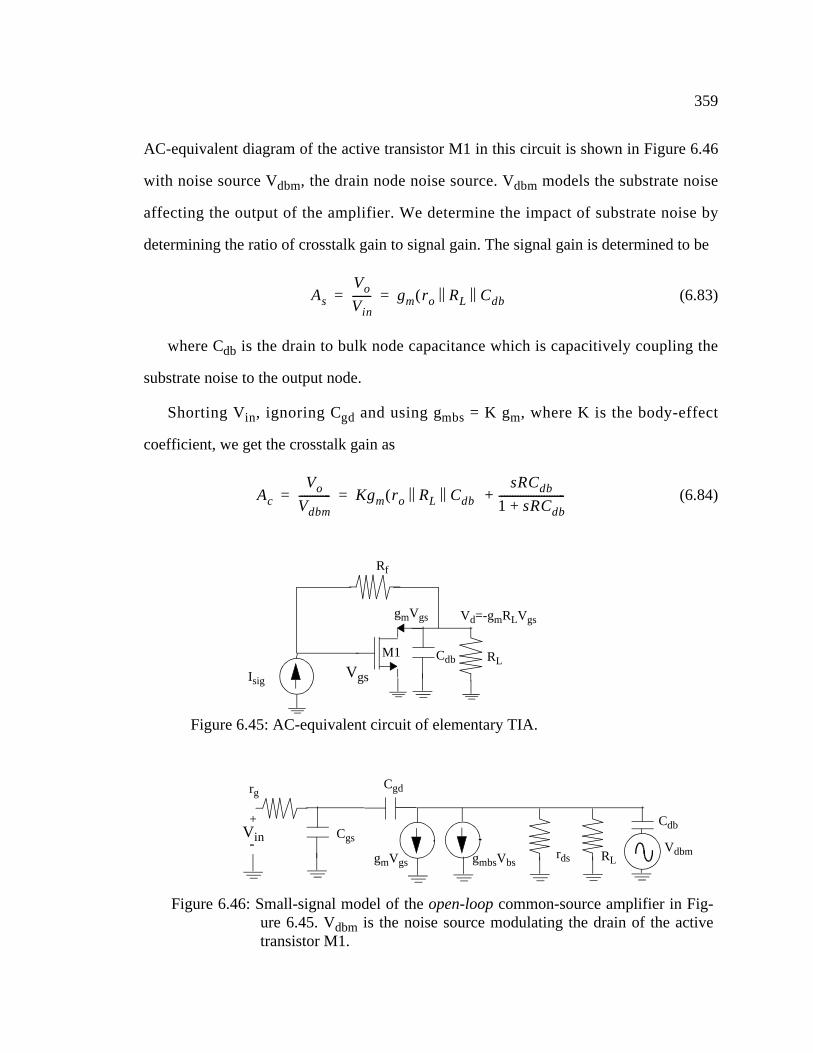
359
AC-equivalent diagram of the active transistor M1 in this circuit is shown in Figure 6.46
with noise source Vdbm, the drain node noise source. Vdbm models the substrate noise
affecting the output of the amplifier. We determine the impact of substrate noise by
determining the ratio of crosstalk gain to signal gain. The signal gain is determined to be
(6.83)
where Cdb is the drain to bulk node capacitance which is capacitively coupling the
substrate noise to the output node.
Shorting Vin, ignoring Cgd and using gmbs = K gm, where K is the body-effect
coefficient, we get the crosstalk gain as
(6.84)
AsVo
Vin------- gm ro RL Cdb|| ||( )= =
AcVo
Vdbm------------ Kgm ro RL Cdb|| ||( )
sRCdb
1 sRCdb+-------------------------+= =
Rf
RL
gmVgs
Vgs
Vd=-gmRLVgs
Isig
Figure 6.45: AC-equivalent circuit of elementary TIA.
CdbM1
Figure 6.46: Small-signal model of the open-loop common-source amplifier in Fig-ure 6.45. Vdbm is the noise source modulating the drain of the activetransistor M1.
rdsgmbsVbsgmVgs
CgsVinRL
Cgdrg
+
-
Cdb
Vdbm

360
The ratio of crosstalk gain Ac to signal gain As becomes
(6.85)
This means that for reducing substrate-coupled crosstalk noise, we have to reduce the
body effect, increase gm and reduce the parasitic capacitance, Cdb, to the bulk at the output
node of the amplifier. However, for a given technology, the only free variable for reducing
Cdb and increasing gm is to have the minimum possible width of the active transistor for
the maximum current flowing through the device, which implies a large gate-overdrive of
the transistor. A large gate-overdrive increases the channel electric-field and increases the
excess channel thermal-noise factor Γ, reducing the sensitivity of the amplifier. The only
practical solution is to choose a circuit topology with minimal parasitic loading to the
substrate with the largest possible output device transconductance and minimal body-
effect. Moving to a differential circuit topology at the front-end improves noise rejection
as well.
6.3.2.7.3 Architecture Choice of Front-End Amplifier
Given that we have been comparing CSTIAs and CGTIAs at a simplistic level, we
compare their sensitivity in earnest. We note that the CGTIA is essentially a CSTIA with a
CG FE. Continuing with the analysis of the CSTIA in Figure 6.39, we note that the full
expression for the input-referred noise PSD is
(6.86)
where CT = Cd + Cg2, Cd=kCg2, ωT=gm2/Cg2. The -3dB frequency of the amplifier is
given by ωB=A/(RfCT) = ωTRd/((k+1)Rf) = ωTRd/ωB, where A = gm2Rd and ωB << ωT,
Rf >> Rd for the input pole to dominate the performance of the CSTIA (input capacitance
> output capacitance). Using Rf = Ak/(ωBCd(k+1)) in Equation 6.85, we get
Ac
As----- K
sCdb
gm-----------+=
SI ω( )4kBT-------------- 1
Rf----- Γ
gm2-------- ωCT( )2 1
Rf2
------+ 1
Rf----- 1
Rd------+
ωCT( )2
gm22
------------------ 1
gm22 Rf
2---------------+
+ +=

361
(6.87)
Note that if the output of the amplifier is a low-impedance output such that the
amplifier has a single-pole response, then the effect of Rd can be ignored and we can write
Rf as a function of Cd. The downside is that we have to accept the gain of the amplifier A,
as an independent bounded variable. Assuming a 2-pole MFM response of the CSTIA
amplifier given in Equation 6.44, we get the -3dB frequency as . Replacing
ωB by in Equation 6.85, using Equation 6.45 and Equation 6.47 for I2 and
I3, we get the input-referred mean-square noise-current of the CSTIA in Equation 6.88. It
is helpful to note that ωB divided by 1.414 gives 4.44 fB.
(6.88)
We account for parasitic capacitance Cp in excess of the photodiode capacitance Cd by
modifying the above analysis such that Cd is replaced by Cd + Cp in Equation 6.87.
(6.89)
(6.90)
Following a similar analysis for the case of the CGTIA, we get
SI ω( )4kBT--------------
ωBCd k 1+( )Ak
------------------------------- 1ΓωB k 1+( )
AωT----------------------------
ωB k 1+( )( )2
AωT( )2-------------------------------+ +
ω2ΓCd k 1+( )2
kωT------------------------------------- 1
k 1+( )ωB
AωTΓ------------------------+
+=
f f 3– 2⁄=
ωB ωB 2⁄=
ieqCS2⟨ ⟩
4kBT-----------------
3.5fB2 Cd k 1+( )
Ak------------------------------------ 1
4.44ΓfB k 1+( )AωT
------------------------------------19.74 ωB k 1+( )( )2
AωT( )2---------------------------------------------+ +
15.52fB3 ΓCd k 1+( )2
kωT------------------------------------------------- 1
4.44 k 1+( )fB
AωTΓ--------------------------------+
+=
∆ kCp 2 k 1+( )Cd+=
YCS k 1+( )Cd kCp+=

362
(6.91)
In Equation 6.91, O is the input-referred mean-square noise-current in Equation 6.88. We
note that as Cp tends to zero, Equation 6.91 tends to Equation 6.88.
Continuing with the CGTIA analysis, the complete expression for the CGTIA input-
referred noise-current PSD, SI(ω), is given by
(6.92)
where Cd=k Cg1, CT= Cg1 + Cd + Cp = ((k + 1)Cd + k Cp)/k, gm1 = m gm2, ωT = gm1/Cg1 =
gm2/Cg2. We also note that the multiplication of the input-referred noise-current PSD by
the term (1 + (ωCT/gm1)2) in Equation 6.92 reflects the integration of the second-stage
CSTIA noise through the CG transistor, whose pole is included in this analysis. Using
Equation 6.89 and defining Y and u as follows:
(6.93)
(6.94)
we get the input-referred mean-square noise-current of the CGTIA amplifier in Equation
6.99, taking into account the CG pole fT/(k+1) and the excess capacitance Cp. The transfer
ieqCG2⟨ ⟩
4kBT------------------ O 0.125ωB
ωB2 ΓCp∆
A2ωTCd
---------------------ωB
3 k 1+( )Cp∆
A3ωT2Cd
-----------------------------------ωBCp
A-------------
ωB3 CpYCS
2
A3ωT2Cd
2-----------------------+ + +
0.0625ωB3 ΓCp∆
ωTCd--------------
ωBCdCp k 1+( )∆
AωT2Cd
2------------------------------------------
ωBCpYCS2
AωT2Cd
2-----------------------+ +
+
+
=
SI ω( )4kBT--------------
Γω2CT2
gm1----------------- Γ
gm2-------- 1
Rf2
------ ωCg2( )2+
1ωCT( )2
gm12
------------------+ ω2CT
2
Rd1gm12
------------------
1Rf----- 1
ωCg2( )2
gm22
-------------------- 1
gm2Rf( )2---------------------+ +
1ωCT( )2
gm12
------------------+
+ +
+
=
YCG ∆kCp ωT2Cd
2⁄=
u f3 k 1+( ) fT⁄=

363
function of the CGTIA is given by Equation 6.95, taking into account the CG pole and
assuming a 2-pole MFM second-stage response.
(6.95)
I2, the second Personick integral [41] for the ZT(f) in Equation 6.95 is evaluated
numerically as
(6.96)
I3, the third Personick integral for the ZT(f) in Equation 6.95 is evaluated numerically as
(6.97)
I5, the fifth Personick integral for the ZT(f) in Equation 6.95 is evaluated numerically as
(6.98)
The total input-referred mean-square noise-current of the CGTIA is the sum of the left
hand side (lhs) terms in Equation 6.100 through Equation 6.104 given by
(6.99)
(6.100)
(6.101)
ZT f( )ZT 0( )
1 jf0.5f3 1 j+( )----------------------------+
1 jf0.5f3 1 j–( )---------------------------+
1 juff3-------+
-----------------------------------------------------------------------------------------------------------=
I2ZT yf3( )ZT 0( )
-----------------2
yd0
∞
∫ f31
1 uy( )2+( ) 1 2y2–( )2
4y2+( )------------------------------------------------------------------------
yd0
∞
∫= =
I3ZT yf3( )ZT 0( )
-----------------2y2 yd
0
∞
∫ f33 1
1 uy( )2+( ) 1 2y2–( )2
4y2+( )------------------------------------------------------------------------y2
yd0
∞
∫= =
I5ZT yf3( )ZT 0( )
-----------------2y4 yd
0
∞
∫ f35 1
1 uy( )2+( ) 1 2y2–( )2
4y2+( )------------------------------------------------------------------------y4
yd
0
∞
∫= =
ieq22⟨ ⟩
4kBT--------------
iI2
2⟨ ⟩
4kBT------------
iI3
2⟨ ⟩
4kBT------------
iI5
2⟨ ⟩
4kBT------------
iI3Y
2⟨ ⟩
4kBT------------
iI5Y
2⟨ ⟩
4kBT------------+ + + +=
iI2
2⟨ ⟩
4kBT------------
4.44f32Cd
Amk--------------------- 1
4.44Γf3
ωTA------------------
19.71f32
ωTA( )2------------------+ +
I2=
iI5
2⟨ ⟩
4kBT------------ 1558.55f3
5 Cd k 1+( )2
mkωT3
-------------------------- Γ4.44f3
AωT---------------+
I5=

364
(6.102)
(6.103)
(6.104)
We compare the input sensitivity results obtained from the full expressions for the
input-referred mean-square noise-current for the CSTIA (Equation 6.91) and the CGTIA
(Equation 6.99), by using Equation 6.35 to obtain the minimum received optical power for
a desired BER, given the input-referred mean-square noise-current in Figure 6.47. The
solid line is the sensitivity curve for the CGTIA amplifier which takes into account the
pole from the common-gate stage. The middle dotted line is the sensitivity curve of the
CGTIA if the CG pole is not accounted for, and the top dotted line is the sensitivity curve
for the CSTIA. The noise reduction in the solid curve corresponds to the band-limiting of
the front-end due to the increasing role played by the CG pole in limiting the contribution
of the amplifier noise through the evaluation of the Personick integrals in Equation 6.96,
Equation 6.97 and Equation 6.98.
iI3
2⟨ ⟩
4kBT------------ 39.5f3
3 ΓCd k 1+( )2
kωT------------------------------ k 1+( )2
ωT2Rd1
-------------------ΓCd
mkωT--------------
4.44f3Cd k 1+( )2
AmkωT2
-----------------------------------------
14.44Γf3
ωTA------------------
19.71f32
ωTA( )2------------------ 1
k 1+( )2-------------------+ + +
+ + +
I3
=
iI3Y
2⟨ ⟩
4kBT------------ 39.5f3
3YCG
ΓωTCd
k----------------- 1
Rd1--------
19.71Γf32Cd
ωTA2mk----------------------------
4.44f3Cd
Amk--------------------- 1
19.71f32
ωTA( )2------------------+
+ + +
I3
=
iI5Y
2⟨ ⟩
4kBT------------ 2π( )4f3
5YCGCd
mkωT-------------- Γ
4.44f3
AωT---------------+
I5=

365
Figure 6.47: Plots of the full CGTIA sensitivity expression (Equation 6.99 and Equation6.35) (solid line), full CSTIA sensitivity (Equation 6.91 and Equation6.35) (dash dot line) and the CGTIA sensitivity expression without takingthe CG pole into account. 0.5 µm CMOS values of m = 8, k = 4, ωT = 44Grad/s, A = 5, Γ = 1.5, BER < 10-13, Cd = 500 fF and Cp = 0 fF are used.
Figure 6.48: Plots of full CGTIA sensitivity expression (Equation 6.99 and Equation6.35). (a) covers k = 1, 2, 4, 8 for m = 8 and (b) shows k = 0.25, 1, 4 form = 8.
(a) (b)
3 dB frequency f-3 (Hz) 3 dB frequency f-3 (Hz)

366
The results indicate that a CGTIA achieves about 3 to 4 dBm improvement than a
CSTIA even after including effects of the parameters of m and k on both the CSTIA and
CGTIA for reducing power consumption. These curves represent the sensitivity floor that
can be achieved for optoelectronic receivers in 0.5 µm CMOS at the data rates determined
by the corresponding -3dB frequency on the X-axis.
In practice, considerations of biasing, power supply and substrate noise rejection and
integrated noise from subsequent amplifier stages reduce the sensitivity that can be
achieved. One limitation of the analysis is that the transistor model equations used to
derive the noise equations is valid only up to 0.3ωT and its error increases as we approach
ωT. The key factor that is influenced in this analysis is the relationship between gm, ωT
and Cgs.
We also check the impact of the parameters of m, k and Cd on the receiver optical
sensitivity of the CGTIA expression in Equation 6.99. Values used are m = 8, ωT = 44
Figure 6.49: Plots of CGTIA sensitivity expression (Equation 6.99 and Equation 6.35).(a) covers the variation of m from 1,4,8,16 for k = 4 and (b) shows thepenalty accrued due to Cp= 0, 100, and 300 fF for k=4, m=8, Cd=500 fF.
(a) (b)
3 dB frequency f-3 (Hz)
3 dB frequency f-3 (Hz)
3 dB frequency f-3 (Hz)

367
Grad/s, A = 5, Γ = 1.5 and BER < 10-13, Cd = 500 fF and Cp = 0 fF, typical of 0.5 µm
CMOS. Figure 6.48 and Figure 6.49 indicate that the sensitivity penalty is acceptable for
the choice of k = 4 and m = 8 and that the penalty due to parasitic capacitance is
approximately 1 dBm for every 100 fF in 0.5 µm CMOS process technology. Extending
these results to a possible 0.1 µm CMOS process technology with fT = 100 GHz and Γ
(excess channel thermal-noise) = 2.5, we compare the sensitivities that can be obtained for
detector capacitances of 500 fF and 100 fF with zero parasitic capacitance, in Figure 6.50.
Figure 6.51 shows the impact of the induced gate-noise on the exact CGTIA (Equation
6.99 and Equation 6.35) and CSTIA expressions (Equation 6.91 and Equation 6.35). We
use the analysis in Section 6.3.2.2 on page 328 to factor in the induced gate-noise by
multiplying the input-referred noise-current PSDs of the transistors by the right-hand side
Figure 6.50: Plots of full CGTIA sensitivity expression (Equation 6.99 and Equation6.35) (solid line), full CSTIA sensitivity (Equation 6.91 and Equation6.35) (dotted line) and the CGTIA sensitivity expression without takingthe CG pole into account (dash dot line) for 0.1 µm CMOS process tech-nology with m = 8, k = 4, fT = 100 GHz, Cp = 0, Γ = 2.5 and BER < 10-13
for the case of (a) Cd = 500 fF and (b) Cd = 100 fF.
(a) (b)
3 dB frequency f-3 (Hz) 3 dB frequency f-3 (Hz)

368
of Equation 6.26. We assume that α = 0.5, the correlation coefficient c = 0.395, the
wavelength of transmission λ = 850 nm, quantum efficiency of the photodiode η = 0.8,
m = 8, k = 4, ωT = 44 Grad/s, Cd = 500 fF, Cp = 0, Γ = 1.5, CG load resistor Rd = 500 Ω,
T = 300 °K, and BER < 10-13. We see that the optical sensitivity of each receiver
corresponding to a frequency on the horizontal axis, is degraded by about 1 dBm in both
the CSTIA and the CGTIA cases. Note that performing the analysis for a more reasonable
junction temperature of 358 °K will also result in the sensitivity curves shifting up,
indicating a degradation in receiver sensitivity.
Figure 6.52 shows the impact of a resistor Rs, in parallel with the photodiode which
keeps the bias current flowing in the CG front-end transistor, on the receiver sensitivity.
Figure 6.51: Plots of exact CGTIA sensitivity expression (Equation 6.99 and Equation6.35) (solid line), full CSTIA sensitivity (Equation 6.91 and Equation6.35) (dash-dot line), the exact CGTIA sensitivity expression withinduced gate-noise (dash dot line) and the full CSTIA sensitivity expres-sion with induced gate-noise for 0.5 µm CMOS process technology withλ = 850 nm, η = 0.8, m = 8, k = 4, ωT = 44 Grad/s, Cd = 500 fF, Cp = 0,Γ = 1.5 and BER < 10-13.
3 dB frequency f-3 (Hz)

369
This bias resistor is typically not used when the data rate is much lower than the device fT
(by a factor of 20 or better). However, when the data rate is close to the device fT, the
output waveforms of the CG front-end are distorted if the devices have to move in and out
of saturation during the course of the signal, as would be the case when the bias resistor is
absent. As the bandwidth of the designed amplifier drops below 1 GHz, the CSTIA
becomes competitive. The noise penalty associated with the biased CGTIA is acceptable
at higher data rates as it may still have a better optical sensitivity compared to the CSTIA
depending on the value of the bias resistor that is needed.
As the bias current in the CG FE transistor increases, the value of the bias resistor
decreases because of the fixed power-supply voltage. This increases the noise penalty
Figure 6.52: Plots of exact CGTIA sensitivity expression (Equation 6.99 and Equation6.35) (solid line), full CSTIA sensitivity (Equation 6.91 and Equation6.35) (dash-dot line) and the exact CGTIA sensitivity expression whichaccounts for a bias resistor Rs = 1.82 KΩ in parallel with the photodiode(dotted line) for 0.5 µm CMOS process technology with λ = 850 nm,η = 0.8, m = 8, k = 4, ωT = 44 Grad/s, Cd = 500 fF, Cp = 0, Γ = 1.5 andBER < 10-13.
3 dB frequency f-3 (Hz)

370
associated with the bias resistor. At lower frequencies, the bias resistor can be removed
and we would consider the solid line in Figure 6.52. Note that the wavelength of
transmission, λ is equal to 850 nm, the quantum efficiency of the photodiode, η, is equal
to 0.8, m = 8, k = 4, the unity current-gain frequency of the CG FE transistor, ωT, is equal
to 44 Grad/s (corresponding to 300 mV of gate overdrive), the photodiode capacitance,
Cd, is equal to 500 fF, Cp = 0, Γ = 1.5, CG load resistor, Rd, is equal to 500 Ω, the
temperature, T, is equal to 300 °K and BER < 10-13.
We try to see if we can improve the OE receiver sensitivity by introducing a noise
minimum at the desired bit rate by a passive element at the front-end, with the least
amount of parasitics, and the least area penalty. A logical choice for this is the bond wire
connecting the photodiode to the optoelectronic receiver front-end. However, with the
drive towards smaller form-factor packages and consequent flip-chip packaging, we
cannot rely on bond wires to provide the necessary inductance. The bond wire connecting
the photodiode to the receiver front-end acts to peak the photodiode capacitance,
offsetting the effect of the photodiode capacitance on the frequency performance of the
receiver. When we examine the impact on receiver sensitivity due to the inductor between
the photodiode and the circuit, we see that the inductor effectively multiplies the input-
referred noise-current PSD of the circuit by . Therefore, if we choose L
appropriately for a given C, then we can reduce the noise by a certain amount at the
operating frequency of .
The transposition of noise sources is schematically indicated in Figure 6.53. The
circuit is assumed to be at the right-hand side of the small-signal model in Figure 6.53 (a)
and (b), whose input-referred noise-current PSD is represented by the noise-current source
i2ckt. C represents the photodiode capacitance and the additional parasitics at the front-
end, and L is the inductance we have chosen to introduce at the front-end. Using the
1 ω2LC–( )2
ω 1 LC⁄=

371
analysis technique we developed in the beginning of the chapter, we apply rules R5 and
R3 (shown in Figure 6.23) repeatedly to get the equivalent circuit in Figure 6.53 (b).
The insertion of an inductor has the attendant consequence of parasitic series
resistance R. This resistance R adds an (ωRC)2 term to the (1 - ω2LC)2 term that
multiplies the input-referred noise-current PSD of the receiver. The effect of R is to reduce
the noise minimum obtained by using the inductor in the input-referred noise-current PSD.
Therefore, a low resistance inductor is desired.
The insertion of an inductor between the photodiode and the CG FE modifies the
transfer function I2/I1 of the CG FE from gm/(gm + jω(Cd+Cgs) to
(6.105)
Assuming that ωT ~= C2/gm, ωo2~= 1/LC1, and that C1 ~= Cd, we get,
Figure 6.53: Schematic illustration of the influence of the front-end inductor on theinput-referred noise-current PSD i2ckt. The transposition is achieved byusing rules R5 and R3 described in Figure 6.23.
ickt2is
2 ickt2is
2 (1-ω2LC)2
L
C
L
CR5, R3
(a) (b)
M1
Figure 6.54: AC-schematic of single-ended CG OE receiver front-end.
L
C1 C2
I1I2
I2
I1---- 1
1 ω2LC1– jω C1 C2+( )
gm---------------------------- ω3LC1C2
gm-----------------–
+--------------------------------------------------------------------------------------------------=

372
(6.106)
where k = Cd/C2 = Cd/Cgs.
Using Equation 6.94 and defining α as
(6.107)
we get
(6.108)
We note that the transfer function in Equation 6.95 is modified such that the (1-juf/f3)
term in the denominator corresponding to the CG transfer function is replaced by Equation
6.106. I2, the second Personick integral [41] for the modified ZT(f) can be evaluated
numerically as
(6.109)
6.3.3 OE Receiver Design in 0.5 µm CMOS
The OE receiver array has to address the key problems of high bandwidth (2.5 Gb/s/
channel), high input-sensitivity, design for power-supply and substrate crosstalk immunity
in array configuration, and minimal power-consumption. The key design issues in receiver
arrays compared to single receivers are the power consumption of individual receiver
I2
I1---- 1
1 ω2
ωo2
---------–
j ω k 1+( )ωT
--------------------- ω3
ωo2ωT
-------------–
+
------------------------------------------------------------------------------=
αfT
fo k 1+( )---------------------=
uαf3
fo----=
I2ZT yf3( )ZT 0( )
-----------------2
yd0
∞
∫
f31
1 αy( )2–( )2
uy( )2 1 uαy( )2
k 1+-----------------–
2
+ 1 2y2–( )
24y2+( )
---------------------------------------------------------------------------------------------------------------------------------------
yd0
∞
∫
=
=

373
channels, the degradation in sensitivity due to channel-to-channel crosstalk and layout
area constraints. Design choices of using inductors to peak circuit elements in the
amplifier chain are unlikely to be feasible due to restrictions on the channel pitch in the
layout such as the need to pitch match to the input fiber-optic ribbon. Additionally, the
power and ground isolation of different receiver channel stages through bond-wire
isolation is limited. Receiver design also includes the issue of low sensitivity of the
receiver performance to input capacitance and process variations.
The design choice of a CG FE serves to separate the time-constants associated with the
photodiode and the closed-loop TIA as indicated in Equation 6.53 and Equation 6.54. This
separation of time-constants gives a weaker dependence of the circuit performance on
input-capacitance. Another way of looking at this is that the CG stage functions much as it
does in a sense amplifier in Static Random Access Memory (SRAM) cores, where a CG
stage is used to isolate the bit-line capacitance from the sensitive input of the sense
amplifier. The sense amplifier amplifies weak signals from the capacitively loaded bit-
lines. Additionally, the performance of a CGTIA is always better than a CSTIA for the
same desired input sensitivity, or equivalently, it is more sensitive than a CSTIA at the
same frequency of operation.
We have established the utility of a CG front-end with k = 4 and m = 8 to achieve a
good balance between power consumption and receiver sensitivity. We have also seen that
an inductor with low parasitics between the photodiode and the input of the CG front-end
can introduce a noise minimum at the desired bit rate. This has to be done carefully
because the input-referred noise increases sharply after the minimum, which means that if
the noise minimum occurs at a lower frequency because of the choice of a larger inductor
than necessary, then the circuit sensitivity at the desired (higher) bit rate will be poorer.
We also established that substrate crosstalk is best reduced for a given CMOS process
technology by moving to a circuit topology with maximum transconductance for the

374
output transistor with the minimum output capacitance loading, and where the output
transistor has minimum body effect. Increasing transconductance at the front-end incurs a
noise and power consumption penalty. Reducing the body-effect implies that the best
circuit architecture is a CS amplifier, from the perspective of reducing substrate crosstalk,
since its body effect coefficient, K, equals zero.
Single-ended receivers have lower input-referred rms noise-current compared to their
differential counterparts. However, it is very hard to get good power-supply rejection ratio
(PSRR) in single-ended receivers and there is no common-mode rejection ratio (CMRR)
in single-ended receivers. Very clean power supplies, supply-independent biasing, and
careful generation of reference signals for decision threshold circuitry add complexity and
potentially degrade the noise performance of single-ended receivers. The closed-loop
amplifier used as the TIA cannot function at as high a frequency as compared to the
differential receiver because the single-ended open-loop amplifier requires three stages in
order to achieve polarity inversion for negative feedback, whereas the differential
configuration requires only two stages.
Power-supply noise at the front-end reduces sensitivity by degrading SNR. Since a
differential circuit configuration offers the advantage of common-mode noise rejection,
we are best served from a circuit point of view, to move to a differential configuration as
early in the signal chain as possible. While we can make all the amplifiers in the receiver
channel differential, the signal coming into the circuit from the photodiode is still single-
ended. This means that any noise on the signal due to sources like power-supply noise on
the photodiode bias circuit, coupled noise from adjacent channels, would not be
diminished by virtue of common-mode rejection. At the same time, we are limited to
using a single photodiode for each channel to convert the incoming light into a current,
which means that we cannot use multiple fibers or devices to generate differential signals.

375
Traditional integrated OE receiver designs bias photodiodes such that one terminal is
connected to a clean bias supply and the other terminal is connected to the input of the
front-end as shown in Figure 6.25 and Figure 6.32. Also, a differential front-end can be
used to amplify the current signal from a single-ended photodiode with a dummy
photodiode or capacitance on the opposite polarity input [26] as shown in Figure 6.55 (b).
A truly differential receiver can be generated from a single photodiode if we can couple
the signal from both terminals of the photodiode into the receiver as differential signals, as
schematically shown in Figure 6.55 (c). The challenge in this kind of design is the biasing
of the receiver front-end. The design has to be able to supply the needed reverse bias of
0.6 to 0.8 V across the photodiode so that it operates efficiently. This impacts noise
performance of the differential receiver because of the noise from two separate circuit
paths. The penalty for unbalanced receiver designs will be higher, especially if the
photodiode bias circuit also biases the differential receiver front-end. Note that in Figure
6.55 (c), the total signal swing into the amplifier has been effectively doubled (due to the
generation of differential signals at the input of the amplifier) even though the input-
referred rms noise-current has increased due to the configuration.
Figure 6.55: Schematic illustration of possible realizations of (a) single-ended and((b) and (c)) differential receivers, all of which operate with light signalfrom a single fiber.
Rf
AvIsig
Rf
AvIsig
Rf
Rf
Av
Isig
Rf
dummydiode or
matchingcapacitance
(a) (b) (c)

376
We choose to adopt the marriage of the front-end design schematic in Figure 6.55 (c),
with the concept of the common-gate front-end in Figure 6.32 as this allows the generation
of a differential signal right from the photodiode and serves to isolate the photodiode
capacitance from the pole of the TIA. We trade-off the benefit in increased power-supply
and substrate immunity, commode-mode rejection and increased gain-bandwidth product
with a penalty of a reduction of receiver sensitivity. The circuit architecture that we
choose to implement at the front-end has to keep in mind the noise penalty of the front-end
biasing circuit.
This requires an isolated PIN diode array where both terminals are free, which is
usually not the case with a PIN array, where one of the terminals is the substrate and is
shared among all the diodes in the array. The AC-schematic of the differential CG OE
receiver with an isolated PIN diode is shown in Figure 6.56, along with input and output
waveforms of the receiver front-end. Ion and Ioff represent the levels of current signal in
the photodiode due to received light power, corresponding to logic high and logic low. In
response to the current flowing in the photodiode, the voltage at nodes A and B go down
from Voff to Vlow and up from Voff to Vhigh, respectively as shown in Figure 6.56. In
response to these waveforms, the output waveforms move up from Vo,off to Vo,high and
down from Vo,off to Vo,low respectively.
Figure 6.56: AC-schematic of the differential CG OE receiver.
Rf
AvIsig
Rf
Vo,off
Vo,high
Vo,off
Vo,low
Vmidh
VmidlVoff
Vhigh
Voff
Vlow
IonIoff
Rd
Rd
Rb
Rb
A
B

377
The necessity of providing 0.6 to 0.8 V of reverse bias across the isolated PIN diode in
Figure 6.56 requires that we incur the noise penalty of biasing resistors Rd and Rb. These
resistors are implemented by transistors even though transistors are likely to have a higher
equivalent input-referred noise-current penalty than real resistors at the same temperature.
The current of a few milliamperes in the CG stage means that the value of the resistors Rd
and Rb is less than a Kilo-ohm, given a power supply of 3.6 V. The large value of this
current means that we cannot use the current path through the output transistor of the TIA
and the feedback resistor of the TIA to supply the CG current. The voltage drop across the
feedback resistor, which is usually large, and the need to optimally bias the TIA, force us
to use Rd in Figure 6.56. Resistors Rd and Rb contribute a large amount of noise-current to
the input of the CGTIA. If Rd and Rb are implemented by real resistors, a large positive
and negative power supply would have to be used in order to increase the value of these
resistors, thereby reducing their noise-current contribution. The introduction of additional
power supplies is not desirable. Resistors implemented by transistors are useful to
accommodate process variations by the use of feedback servo control. Since node A has to
be at a higher voltage than node B, we choose the front-end design in such a way that this
biasing consideration is met as well.
We solve this problem by replacing the CG transistor in the lower arm of the receiver
front-end by two CG transistors in series, to lower the bias voltage at the positive terminal
of the PIN diode (node B) in Figure 6.56. This technique reduces the noise penalty
associated with the channel hot electrons to a minimum and gives some additional peaking
in the circuit response.
Biasing is a matter of serious concern at the front-end, because fluctuations in the bias
levels of the front-end transistors results in dramatic changes in the circuit behavior due to
changes in operating-point of the transistors. Also, it is desirable to ensure that bias-points
are maintained at their desired values independent of process variations.

378
Traditional techniques of biasing involve a core bias-generator circuit on the IC, which
generates bias voltages and currents nominally independent of the power supply, and
either proportional to absolute temperature (PTAT) or independent of temperature. This
technique relies on the fundamental assumption that the differences in power and ground
voltages due to IR drop variations (which depend on the values of the current, I, consumed
by the circuit and the resistance, R, of the power/ground distribution network) are small,
so that the same circuits located at different parts of the IC operate the same way. This is
usually not the case with high data-rate CMOS circuits where the transistors operate very
close to fT, and burn more power than their bipolar counterparts. It is therefore, better to
have local bias-generators that generate bias voltages and currents for each channel.
We choose to bias the receiver circuit using feedback-servo circuits to make the circuit
performance independent of process variations. The feedback-servo circuits take an off-
chip reference voltage and apply the appropriate voltage at the gate of the controlled
transistor to make the measured drain or source voltage equal to the external reference
voltage, which is supplied to the IC through pads with a low-pass filter having a cut-off
Figure 6.57: Schematic illustration of bias servoing using a dummy amplifier.
M1p
M3p Av
Av
M2p
to dummy TIA input.
M1
M3
M2
to second CG front-end
Vbias1
Vbias2
to TIA inputI = 2.2 mAgm = 10.8 mS (slow library models, 85 degrees Celsius)300 mV gate overdrivefT = ~ 10 GHz

379
frequency of 100 KHz. It is not feasible to sustain the loading of the feedback-servo
circuits in the signal path for high data rate receiver circuits as they add parasitic
capacitance and can be potentially unstable. Consequently, we create a dummy receiver
front-end by copying the layout. We monitor the node voltages of the dummy receiver and
use voltage-follower circuits to servo the sensitive bias points to external reference
voltages. An example of this is shown in Figure 6.57 for one of the CG inputs of the
receiver FE. Transistor chain M1p, M2p and M3p constitute the dummy receiver’s CG
receiver front-end, which is a copy of the main receiver’s CG front-end composed of M1,
M2 and M3. The negative terminal of the isolated PIN is connected to this CG front-end.
Voltage followers servo the gate voltages of M1 and M3 so that their source and drain
voltages correspond to Vbias2 and Vbias1 respectively. The reference voltages Vbias1 and
Vbias2 could be from external voltage sources or from internal bias-generation circuitry.
This technique is used to bias the receiver CGTIA and the succeeding amplifier stage to
correct the DC-offset of the differential output signals (as drawn in Figure 6.56) of the first
stage.
The use of inductors to improve OE receiver performance has been analyzed for
single-ended GaAs OE receivers in the literature [194]. Inductors have also been used to
increase the open-loop gain and reduce the input-referred noise-current of amplifiers used
for TIAs in GaAs [193]. Inductors have also been used to improve the simulated
performance of CMOS TIAs by peaking the photodiode capacitance in a conventional
single-ended TIA [195]. The value of the inductor reported was 1.5 mH and the design
used +5 and -5V power supplies, which are not supported for CMOS processes, especially
finer feature size CMOS. There has been no reported use of inductors to introduce a noise
minimum at a desired operating bit rate. Other inductive structures, like Bridged T-Coil
matching networks [198], though attractive from the viewpoint of improving bandwidth
by separating in time the charging of parallel capacitance and resistance, are meant for

380
voltage input amplifiers. The input-referred rms noise-current penalty of a small resistor at
the input of the amplifier, which sets the input impedance looking into the Bridged T-Coil,
and lowers the time-constant associated with the photodiode capacitance, is too high for
OE receivers.
We introduce inductors between the terminals of the isolated PIN and the CGTIA to
introduce a noise minimum corresponding to 2.5 Gb/s operation of the CGTIA (Figure
6.53). Since it is desirable to reduce the parasitic resistance, capacitance and the area
associated with the inductors, we use a circuit configuration that increases the effective
inductance of each inductor by mutual coupling. The equations describing the behavior of
coupled inductors are given by Equation 6.110, Equation 6.111 and Equation 6.112.
(6.110)
(6.111)
(6.112)
The coupled inductors that form the transformer are oriented in a manner that
reinforce or oppose the magnetic fields in the coils, giving rise to positive or negative
coupling coefficient K (Equation 6.112). A configuration in which the constituent coils
are oriented in such a way that their magnetic fields oppose each other is shown in Figure
6.58 (a). This configuration may be used in a narrow band (tuned) differential amplifier
[197] where the DC-currents of the differential NMOS pair flow into the input ports
labeled in1 and in2. The output ports out1 and out2 may be connected to the power supply.
Note that in such a configuration, where dI1/dt = -dI2/dt and for equal coil inductances L1=
L2 = L, the effective inductance becomes (1 + M)L for each arm of the differential
amplifier for differential operation.
V1 L1 tddI1 M
tddI2+=
V2 Mtd
dI1 L2 tddI2+=
K ML1L2
----------------=

381
As may be seen from Figure 6.56, the current flowing into and out of the isolated PIN
diode has the same direction of rate of change, unlike the currents in the two arms of a
differential pair. In this case, the voltages at the terminals of the isolated PIN diode have
opposite rates of change. Since the variable of interest is current, the coils of the
transformer are oriented in such a way that each current flowing into and out of the
isolated PIN diode generates a magnetic field which reinforces the other as shown in
Figure 6.58 (b). As the input currents increase due to the arrival of a pulse, the generated
fields increase, reinforcing each other and increasing the effective inductance to (1 + M)L,
assuming that the inductance of each planar coil is equal to L.
.
The advantages of using a coupled planar transformer in Figure 6.58 (b) to implement
inductors at the front-end are
• Reduced area penalty compared to two separate coils.
• Reduced R and C parasitics due to smaller coils for a desired L.
• Improved rejection of common-mode noise due to the proximity of the coils.
• Avoidance of the Miller capacitance multiplication effect between coils in
configuration of Figure 6.58 (b) compared to the configuration of Figure 6.58 (a).
Figure 6.58: Coupled planar transformer to increase effective inductance by negative mutual coupling (a) and positive mutual coupling (b).
in1
out1
in2
out2
out1
in1
in2
out2
(a) (b)
B out of page
B into page
B = Magnetic Field
B B

382
We use a Practical Extraction and Report Language (PERL) script “spiral.p” [200] to
automatically generate magic [201] VLSI layout files of transformers with the desired
number of turns for the two coupled planar coils, given a desired area of the transformer.
Patterned ground shields [202] are automatically generated during transformer layout
generation by the PERL script “spiral.p”. The patterned ground shield increases the
quality factor of the inductors comprising the transformer by reducing the eddy current
losses in the substrate. The script also generates an input file for FASTHENRY [203], a 3-
D inductance extraction program which produces a spice sub-circuit corresponding to the
inductance and resistance of the described transformer. We then use HSpice [204] to
generate a more physical sub-circuit of the FASTHENRY model. This sub-circuit is then
used in HSpice simulations of the receiver channel for noise and transient analysis.
The inductors are implemented in third-level metal in 0.5 µm CMOS technology with
a dedicated segmented-polysilicon ground plane which is connected to the ground-return
path of the first stage. This ground return-path is separate from the ground return-path of
the rest of the receiver channel. Transformer parameters are determined to implement a
noise minimum between 2 and 2.5 Gb/s after determining the optimal trade-off between
power consumption and input sensitivity. This consideration is very heavily influenced by
biasing. A design target of 0.5 pF PIN capacitance with 100 fF PIN pad capacitance on
each PIN terminal, and 100 fF pad capacitance on the IC was assumed. The penalty of this
front-end is reduced sensitivity beyond 2.5 Gb/s than one would have expected without
the transformer.
Since the current from the photodiode is very small, we would like to achieve a current
multiplication effect before we couple the current signal from the photodiode into the
front-end input of the receiver. The limiting factor in this approach is the thermal noise of
the bias circuit required to bias the photodiode in the context of the low power-supplies
that are required by the 0.5 µm CMOS process technology. Transformers are not suitable

383
for current multiplication because they need a very small resistance as the secondary load
to realize the current multiplication.
The TIA which follows the CG receiver FE is implemented as a cascoded differential
amplifier (Figure 6.59) to increase gain and bandwidth even though the use of cascode
transistors results in a noise penalty of about 20%. We do not use the broadbanding circuit
technique of a negative resistance implemented by a cross-coupled pair (as in a current
controlled latch), since this circuit configuration increases the input-referred noise-current
at the CG input. Viewed in another way, the jitter at the amplifier output would be higher
due to the inherent uncertainty in the switching threshold of the high-gain cross-coupled
pair. In Figure 6.59, the differential input pair M1 - M2 is operated with 300 mV of gate
overdrive, with a source potential of 0.55 V to minimize the body effect, and to reduce the
substrate coupling effects (Equation 6.85). The feedback resistors are implemented using
transistors M6 and M7 to minimize the parasitic capacitance associated with the resistors.
Resistor Rgf is connected to the gates of M6 and M7 to increase the closed-loop bandwidth
[205]. We use a level shifted PMOS transistor (Figure 3.5) whose input impedance is
given by Equation 3.11 to reduce the parasitic capacitance at the amplifier output due to
the load device. Inductors could used at the source of the PMOS load transistors to extend
the bandwidth by introducing some peaking [193]. These inductors can also be
implemented by coupled planar transformers to advantage as indicated in Figure 6.58 (a).
However, we lack adequate layout space in our array design to include them. Note that we
use a single stage to maximize bandwidth and phase-margin. Even so, the parasitics of the
technology restrict the bandwidth that can be realized by the close loop TIA to
approximately 1.0 GHz across all process corners, which results in a TIA gain of 1500
ohms at 1.5 Gb/s and approximately 750 ohms at 2.5 Gb/s.

384
The stage following the CG OE receiver is a differential DC-level restorer circuit
shown in Figure 6.60 that takes the output of the CG receiver output shown in Figure 6.56
and converts it to a true differential waveform with a common-mode bias voltage. This is
accomplished by adopting an input-pair topology that has been used to reduce duty-cycle
distortion in delay locked loops [206]. The basic operation of the circuit is to filter the
Iin+ Iin-
Vo-
M1 M2
vbias1
Figure 6.59: Schematic of TIA implemented by differential cascoded amplifierwith shunt-shunt feedback.
Ib = 2.86 mAM7
Vbias2 Vbias2
Vo+
M3 M4M5 M6Rgf Rgf
Vin+ Vin-
Vo-
M1 M2
vbias1
Figure 6.60: Schematic of DC-restorer circuit implemented by differential cascodedamplifier with gmboosting and shunt-shunt feedback.
Ib = 2.86 mAM5
Vbias2 Vbias2
Vo+
M9 M10M7 M8
Rgf Rgf
M3 M4
vbias1Ib = 2.86 mAM6
Vin+
Iboost Iboost
Vbiasp Vbiasp
Vo+
Vo-
Vi,off
Vi,lowVmidl
Vi,off
Vi,highVmidh

385
differential waveforms at different DC-levels in order to add or subtract current
differentially from the outputs of the differential pair, whose inputs are driven by the
differential waveform with different DC-levels. To increase the gain of the circuit and to
reduce process variations, we use a gm-boosting circuit [207] to increase the
transconductance gm of the input pair, while keeping the load-transistor drain-current low
and resistance high. We combine it with a shunt-shunt feedback circuit that provides the
facility to control the gain of the DC-level restorer circuit by changing the value of the
shunt-shunt resistor. The load transistors’ gate bias voltage and the bias voltage of the
current source Iboost in Figure 6.60 are set by feedback-servo control using the method in
Figure 6.57.
We minimize ISI effects by using limiting amplifiers based on the concept of Cherry-
Hooper limiting amplifiers [210], which maximize bandwidth by cascading maximally
mismatched amplifiers. An example is a transconductance amplifier driving a
transimpedance amplifier. We use a cross-coupled transistor pair as in a current-controlled
Figure 6.61: Schematic of Cherry-Hooper limiting amplifier with APLSD load (insert (Figure 3.10)) and cross-coupled pair to broadband the amplifier.
M1
M2
M7 M8
M3
M4
M5
M6
M9
Vbias
+-+-Vin+
Vin-
Vout+
Vout-
TransconductanceAmplifier
TransimpedanceAmplifier
Cross-coupled pairto broadband amplifier
APLSD load (Figure 4.46)
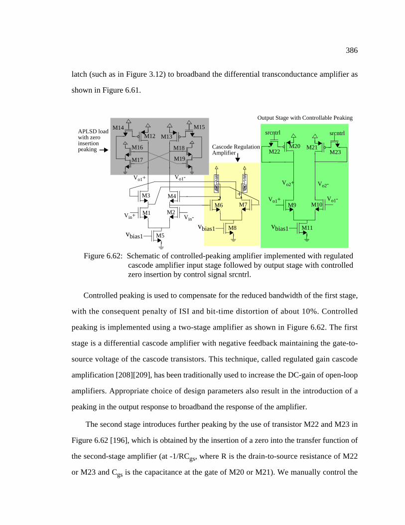
386
latch (such as in Figure 3.12) to broadband the differential transconductance amplifier as
shown in Figure 6.61.
Controlled peaking is used to compensate for the reduced bandwidth of the first stage,
with the consequent penalty of ISI and bit-time distortion of about 10%. Controlled
peaking is implemented using a two-stage amplifier as shown in Figure 6.62. The first
stage is a differential cascode amplifier with negative feedback maintaining the gate-to-
source voltage of the cascode transistors. This technique, called regulated gain cascode
amplification [208][209], has been traditionally used to increase the DC-gain of open-loop
amplifiers. Appropriate choice of design parameters also result in the introduction of a
peaking in the output response to broadband the response of the amplifier.
The second stage introduces further peaking by the use of transistor M22 and M23 in
Figure 6.62 [196], which is obtained by the insertion of a zero into the transfer function of
the second-stage amplifier (at -1/RCgs, where R is the drain-to-source resistance of M22
or M23 and Cgs is the capacitance at the gate of M20 or M21). We manually control the
Vin+ Vin-
Vo1-
M1 M2
vbias1
Figure 6.62: Schematic of controlled-peaking amplifier implemented with regulatedcascode amplifier input stage followed by output stage with controlledzero insertion by control signal srcntrl.
M5
Vo1+
M3 M4 +-M6 M7
vbias1 M8
M9 M10
vbias1 M11
Vo1+ Vo1-
Vo2-Vo2+
srcntrl srcntrlM12 M13M14 M15
M16
M17
M18
M19
M20 M21M22 M23
APLSD loadwith zeroinsertion peaking Cascode Regulation
Amplifier
Output Stage with Controllable Peaking

387
gate voltage of these transistors (thereby changing R) to change the location of the zero in
the transfer function, controlling the amount of peaking and the frequency at which the
gain peaking occurs. This concept is also used to peak the first stage slightly in addition to
the second-order transfer function of the APLSD load (transistors M12-M19). Limiting
amplifiers (Figure 6.62) are used between controlled-peaking amplifiers to restore the
data-eye.
The effect of the reduced bandwidth of the first stage and the controlled peaking in the
post-amplifiers, is higher output jitter and poorer output phase-margin. To improve this,
we use the availability of the clock channel in the synchronous parallel data link to retime
the data. Retiming a half-speed data signal requires the clock to be at twice the bit rate in
bits per second, so that we can latch the input at a specified edge (either falling or rising
edge), which occurs only once per bit.
In order to retime a half-speed data signal, we latch the data stream into separate flip-
flops on the rising and falling edges of the clock, effectively performing a 1:2
demultiplexing operation. We multiplex the data as shown in Figure 6.63 to get back the
half-speed data stream. The HSDFFs in Figure 6.63 correspond to high-speed differential
flip-flops in Figure 3.12. The 2:1 multiplexer in Figure 6.63 is implemented by the merged
multiplexer-limiting amplifier shown in Figure 6.64.The implementation of the
multiplexer as a modified transconductance amplifier stage driving a low input-impedance
Figure 6.63: Schematic of differential retiming circuit.
HSDFF
+-
D1
D2+
s-
s
OUT+,OUT-
D1+,D1-
D2+,D2-
HSDFF
+-
q1+,q1-
clk-
clk+
mux

388
transimpedance amplifier stage effectively allows us to reduce the load capacitance seen
by the high-speed differential flop-flops, as they can be implemented with smaller
devices. This reduces the capacitive load seen by the clock-channel drivers. This method
has the disadvantage that it depends on the duty-cycle of the clock to prevent eye-width
distortion of the retimed output.
The clock signal from the designated clock-receiver channel follows an amplification
path similar to the data. It is then amplified and distributed to all data channels such that
the total simulated end-to-end skew is under 22 ps. The clock signal is then used to retime
the half-speed data by demultiplexing the data and then multiplexing it up again.This
process cleans up the data output eye-diagram, improves the sensitivity of the channel,
and provides acceptable output eye-diagrams for higher sensitivities compared to the case
without retiming. Also, we take care to design the channels to be robust to power supply
and substrate noise, since we integrating the receiver array design in a digital environment
with clock distribution circuitry, demultiplexer and multiplexer circuits. Retiming the
post-amplifier output effectively provides additional gain, cleans up the data output eye-
Figure 6.64: Schematic of merged 2:1 multiplexer and limiting amplifier inFigure 6.61.
Mb1
Mb2
Mb7 M8
M3
M4
M5
M6
M9
Vbias
+-+-Vout+
Vout-
TransconductanceAmplifier
TransimpedanceAmplifier
Cross-coupled pairto broadband amplifier
APLSD load (Figure 4.46)
Ma1
Ma2
a
a
b
b
Ma7clk+ clk-

389
diagram, reduces jitter and minimizes skew. Each channel has source-terminated LVDS
drivers which supports both source and parallel load termination for optimal high-
performance results. The output drivers also employ peaking to reduce the impact of
package and board interconnect loss.
Additionally, we distribute the power and ground pads to isolate the power and ground
for each channel, as well as for each receiver front-end and each output-driver and post-
amplifier circuit. This should increase the performance of the sensitive front-end amplifier
to reject noise on the front-end power and ground rails beyond the simulated value of
10 mV.
6.3.3.1 Measured Results of the 0.5 µm CMOS OE Receiver Array
Figure 6.65 shows the die photograph of the OE receiver array in 0.5 µm CMOS. The
die measures 6.85 mm x 2.9 mm and consumes 3.7 W from a 3.6 V power supply. The OE
receiver array IC is designed as a latched receiver array for half-speed parallel optical data
buses as shown in the IC schematic in Figure 6.66. The clock channel is a designated
6.85 mm
Figure 6.65: Micro-photograph of OE receiver array in 0.5 µm CMOS technology.The submitted layout size is 6.40 mm x 2.7 mm and the IC die size is6.85 mm x 2.9 mm.
d0 d1 d2 d3 d4 clk d5 d6 d7 d8 d9 d10
2.9m
m
Clo
ck C
hann
el
Front-End TransformerPost
Am
p
TIA
Dem
ux/
Mux

390
channel (channel #6 counting from the left in the die photograph). This channel generates
the clock channel that retimes the data across all the 11 data channels to provide nominally
deskewed data outputs at the output pads of the IC. The clock skew on the IC was
simulated to be approximately 22 ps.The output drivers also employ peaking to reduce the
impact of package and board parasitics. Figure 6.66 shows the schematics of the unlatched
and latched TIAs. The relatively modest technology of 0.5 µm CMOS process limits the
TIA bandwidth to approximately 1.0 GHz, resulting in a TIA gain of 1500 ohms at 1.5 Gb/
s and approximately 750 ohms at 2.5 Gb/s.
6.3.3.2 Summary of Results
The OE receiver array was tested electrically with AC-coupled differential signals and
approximately 150 fF of capacitance. Measurements of the OE receiver array indicate a
sensitivity of approximately -20 dBm, -19 dBm and -16.6 dBm for 1.5, 2.0 and 2.5 Gb/s,
respectively, for 223-1 NRZ PRBS at a BER < 10-12. The array, which includes source-
terminated LVDS drivers, consumes 3.7 Watts from a 3.6 V power supply.
The representative electrical data sensitivity of a channel in the latched 0.5 µm CMOS
OE receiver array is shown in Figure 6.67 (a) for 27 - 1 and (b) for 223 - 1 NRZ PRBS
input data patterns at data rates of 1.5 Gb/s, 2.0 Gb/s and 2.5 Gb/s. The curves illustrate
front-end
Post-Amplifier
(1500 Ω at 1.5 Gb/s~750 Ω at 2.5 Gb/s)
out+
out-Latch
Half-speeddata fromsingle fiber
Figure 6.66: Schematic of latched TIA array.
out+
out-
output stage
output stage
Half-speedclock fromsingle fiber

391
the significant increase in noise penalty (degradation in sensitivity) when the data rate is
increased from 2.0 Gb/s to 2.5 Gb/s. This degradation is most likely due to the coupled
planar-transformer induced noise-minimum occurring at a frequency lower than that
required to support 2.5 Gb/s operation. Diamonds, squares and pentagrams correspond to
1.5 Gb/s, 2.0 Gb/s and 2.5 Gb/s respectively.
The measured sensitivity curve for a representative 2.5 Gb/s data channel in the OE
receiver array is shown in Figure 6.68 for 27 - 1 NRZ PRBS, 223 - 1 NRZ PRBS and 231 -
1 NRZ PRBS input data patterns. The inset shows the eye-diagram of the electrical output
driver corresponding to -16 dBm 231 - 1 NRZ PRBS input data patterns and BER < 10-12.
The clock channel signal is also at -16 dBm. The vertical scale is 50 mV/div and the
horizontal scale is 100 ps/div. The measured eye-width and eye-height at the eye-edge
threshold setting of < 10-7, are 285 ps and 77 mV respectively.
The measured sensitivity curve for a representative 2.0 Gb/s data channel in the OE
receiver array is shown in Figure 6.69 for 27 - 1 NRZ PRBS, 223 - 1 NRZ PRBS and 231 -
1 NRZ PRBS input data patterns. The inset shows the eye-diagram of the electrical output
driver corresponding to -19 dBm 231 - 1 NRZ PRBS input data patterns and BER < 10-12.
The clock channel signal is also at -19 dBm. The vertical scale is 50 mV/div and the
horizontal scale is 100 ps/div. The measured eye-width and eye-height at the eye-edge
threshold setting of < 10-7, are 399 ps and 111 mV respectively.
The measured sensitivity curve for a representative 1.5 Gb/s data channel in the OE
receiver array is shown in Figure 6.70 for 27 - 1 NRZ PRBS, 223 - 1 NRZ PRBS and 231 -
1 NRZ PRBS input data patterns. The inset shows the eye-diagram of the electrical output
driver corresponding to -19 dBm 231 - 1 NRZ PRBS input data patterns and BER < 10-12.
The clock channel signal is also at -19 dBm. The vertical scale is 50 mV/div and the
horizontal scale is 200 ps/div. The measured eye-width and eye-height at the eye-edge
threshold setting of < 10-7, are 500 ps and 106 mV respectively.

392
Figure 6.67: Measured sensitivity curves for 1.5 Gb/s, 2.0 Gb/s and 2.5 Gb/s for (a)27 - 1 and (b) 223 - 1 NRZ PRBS input data patterns.
(a) (b)
Figure 6.68: Measured sensitivity curve for the latched TIA at 2.5 Gb/s for 27 - 1,223 - 1 and 231 - 1 NRZ PRBS input data patterns. The insert shows theeye diagram of the channel output at a BER < 10-12 for -16 dBm 231 - 1NRZ PRBS input data patterns and -16 dBm clock inputs from the
100 ps /div
50 m
V/d
iv
The vertical scale is 50 mV/div and the horizontal scale is 100 ps/div.The measured eye-width and eye-height at the eye-edge threshold settingof BER < 10-7, are 285 ps and 77 mV respectively.

393
Figure 6.69: Measured sensitivity curve for a representative OE receiver array channel at 2.0 Gb/s for 27 - 1, 223 - 1 and 231 - 1 NRZ PRBS input data patterns. The insert shows the electrical output eye diagram at a BER < 10-12 for -19 dBm 231 - 1 NRZ PRBS input data patterns and -19 dBm clock inputs.
100 ps /div
50 m
V/d
iv
Figure 6.70: Measured sensitivity curve for a representative OE receiver array channel at 1.5 Gb/s for 27 - 1, 223 - 1 and 231 - 1 NRZ PRBS input data patterns. The insert shows the electrical output eye diagram at a BER < 10-12 for -19 dBm 231 - 1 NRZ PRBS input data patterns and -19 dBm clock inputs.
200 ps /div
50 m
V/d
iv

394
Some of the curves do not follow the classic BER versus SNR curves because the
curves represent latched amplifier sensitivity curves, with the clock amplitude not always
the same as the data amplitude.
Figure 6.71 shows the jitter measurements at (a) 2.5 Gb/s and (b) 1.5 Gb/s at their
respective minimum sensitivities for BER < 10-12. The jitter measurement is better for the
2.5 Gb/s case than for the 1.5 Gb/s case because of the difference in the “operating point”
which can be understood from the sensitivity curves for 2.5 Gb/s (Figure 6.69) and 1.5 Gb/
s (Figure 6.70). The actual signal amplitude reaching the OE receiver channel at 1.5 Gb/s
(-19 dBm) is much smaller than the actual signal amplitude reaching the OE receiver
channel at 2.5 Gb/s (-16 dBm). This difference in signal amplitude accounts for the
apparent improvement in jitter at 2.5 Gb/s as shown in Figure 6.71. The slope-error in the
jitter histogram for the 1.5 Gb/s case (Figure 6.71 (b)) also contributes a small amount to
the difference in jitter between the two cases.
(b)(a)
Figure 6.71: Measured output jitter of a representative OE channel at (a) 2.5 Gb/s for -16 dBm and (b) 1.5 Gb/s for -19 dBm 231 - 1 NRZ PRBS input data patterns and clock signals. The jitter is measured to be (a) 12.47 ps rms (82 ps peak-to-peak) and (b) 14.35 ps rms and 94 ps peak-to-peak.
395
6.4 Summary
In this chapter, we have demonstrated that the high-speed electrical output drivers
used in the PONIMUX IC and the PONI ROPE MUX/DEMUX chipset can drive low-
threshold oxide-confined VCSELs at 2.5 Gb/s while consuming 7.22 mW from a 3.6 V
power supply. We have also demonstrated a -16 dBm 231 - 1 NRZ PRBS 2.5 Gb/s OE
receiver array in relatively modest 0.5 µm CMOS process technology with fT = ~10 GHz.
We started with a system perspective on the EO-OE link which emphasized the need for
reducing the total link-loss to improve the achievable bit rate for low-power consumption
in CMOS. We then used a simplified MOSFET noise model to apply optimal noise design
considerations to various OE receiver architectures to show that the power consumption of
the first two stages (CG, CS) versus receiver sensitivity has a slope of -5 dBm/decade of
power consumption. We have also shown that the power consumption is proportional to
the third power of the OE transducer parasitic capacitance. This makes it all the more
pressing to reduce the parasitic capacitance to improve power consumption and input
receiver sensitivity. Although we started out with a simplified analysis, it gave insight to
the trade-offs encountered. We also showed that the simplified analysis is easily modified
to account for the induced gate-noise, which is likely to be increasingly important in finer
feature size CMOS process technologies. Finally, we detailed the specific design
techniques to achieve our -16 dBm 2.5 Gb/s/channel OE receiver array, which we believe
can be extended to finer feature size CMOS process technologies. The impact of increased
gate-noise and threshold-voltage variations across the IC in finer feature size CMOS
process technologies, the reduced power-supply voltage and the consequent impact on OE
receiver array architecture is not clear at this point.

396
Chapter 7
Feasibility of A 100 Gb/s Parallel Optical Data Link
In this dissertation, we have demonstrated a 12-channel 2.5 Gb/s/channel parallel OE
data link using relatively modest 0.5 µm CMOS process technology, as shown in Figure
7.1. The key components of a 12-channel 2.5 Gb/s/channel multiplexer array with an
integrated sub-50 ps peak-to-peak jitter x4 PLLFS (Chapter 5), a 12-channel 2.5
Gb/s/channel demultiplexer array with aligner circuitry (Chapter 5), and a 12-channel
latched OE receiver array with -16 dBm sensitivity for 2.5 Gb/s/channel 231-1 NRZ PRBS
input data patterns (Chapter 6) have been demonstrated. We have also demonstrated that
VCSEL Array
PINArray
5 Data
1 Frame
1 Clock
5 Data
7 Watts3.7 Watts
3.1 Watts
625
Mb/
s/C
hann
el
625
Mb/
s/C
hann
el
2.5 Gb/s/ChannelMMF-ribbon at 850 nm
Tx Array with x4 PLLFS
OE Rx ArrayRx Array withAligner
Figure 7.1: Proven design point of 25 Gb/s in 0.5 µm CMOS process technol-ogy over 12-wide MMF-ribbon with 10 channels of data.

397
the CMOS VCSEL driver array (Chapter 6) is the same as our electrical high-speed output
drivers, with the distinction that the VCSEL drivers consume less current. The OE
receiver array has clock distribution circuitry and 2:1/1:2 demux/mux circuitry integrated
on the IC to perform the function of retiming the half-speed input data patterns with a half-
speed clock.
100 Gbit/s Ethernet is a natural extension of the movement in the industry, which is
already moving from 1 Gb/s Ethernet, which has been deployed, to 10 Gbit/s Ethernet,
which is undergoing standards-committee work. 1 Gb/s Ethernet has been implemented
entirely in CMOS. It is likely that 10 Gb/s Ethernet will evolve to a standard using four
3.125 Gb/s WDM channels, that is, a four-wide parallel interface to optics. The aggregate
data-rate of 12.5 Gb/s reflects the use of a 25% overhead 8b/10b code. Another version
will be a serial solution at a line-rate of 10.3125 Gb/s, which exploits a 64b/66b code.
What is the feasibility of realizing a 100 Gb/s data-bandwidth parallel OE transmitter
and receiver array with 10 data channels, each running 10 Gb/s in parallel, using 0.1 µm
CMOS process technology, with the use of a low-overhead code such as the 64b/66b code
which is used in 10 Gb/s Ethernet? A parallel interface would mean that we can leverage
our parallel OE interconnect experience to WDM over a Single-Mode Fiber (SMF)
(Figure 7.2). Parallel data transmission using WDM with the same number of wavelengths
Figure 7.2: Block diagram of 12 channel 100 Gbit/s WDM link leveraging advancesin parallel OE data links.
Existing
transmitterarray withmux &clocking
parallelExistingparallelReceiverarray with demux &clocking
12 12
Optical Mux OpticalDemux
single mode fiber

398
as fibers in the fiber-optic ribbon can be essentially considered a transparent replacement
of the fiber-optic ribbon transmission medium from the perspective of the electronic
transmit and receive circuitry. The multiplexing and demultiplexing functions associated
with WDM will be performed in the optical domain, with, for example, low-cost silica
combiners and plastic waveguide-based demultiplexers [212]. This requires appropriate
spacing of wavelengths (channels), to lower the requirements on the lasers and the cost of
the multiplexer and the demultiplexer components.
The advantage of going to WDM over SMF is that the data transmission is essentially
limited by the chromatic dispersion in the fiber (we assume the polarization mode
dispersion is negligible), as shown in Figure 7.3 (b), which is approximately 5 ps/(nm km)
for a 55 nm wavelength window (±27.5 nm) around a center wavelength of 1300 nm
[213]. Therefore, the fiber dispersion for 12 channels at a spacing of 5 nm gives 55 ps/km
of skew. The center wavelength of 1300 nm is a good choice because of the following
reasons:
1. The existing installed base of fiber
2. The low attenuation of 0.4 dB/km (compared to 2 dB/km at 850 nm) in fiber
Figure 7.3: (a) Eye-safe power levels for wavelengths between 700 and 1400 nm and(b) Dispersion curves for wavelengths between 1000 and 1600 nm forSMF with zero chromatic dispersion at 1300 nm.
-10
800 1000 1200
20
10
0
Class 3A
Class 1
λ (nm)
dBm
-10
800 1000 1200
20
10
0
Class 3A
Class 1
800 1000 1200
20
10
0
Class 3A
Class 1
λ (nm)
dBm
ps/(
ns •
km)
λ (nm)
dBm
(a) (b)
λ (nm)
Waveguide Dispersion
Chromatic Dispersion
Material Dispersion
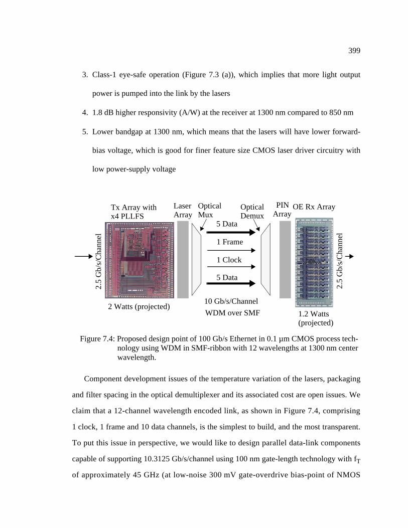
399
3. Class-1 eye-safe operation (Figure 7.3 (a)), which implies that more light output
power is pumped into the link by the lasers
4. 1.8 dB higher responsivity (A/W) at the receiver at 1300 nm compared to 850 nm
5. Lower bandgap at 1300 nm, which means that the lasers will have lower forward-
bias voltage, which is good for finer feature size CMOS laser driver circuitry with
low power-supply voltage
Component development issues of the temperature variation of the lasers, packaging
and filter spacing in the optical demultiplexer and its associated cost are open issues. We
claim that a 12-channel wavelength encoded link, as shown in Figure 7.4, comprising
1 clock, 1 frame and 10 data channels, is the simplest to build, and the most transparent.
To put this issue in perspective, we would like to design parallel data-link components
capable of supporting 10.3125 Gb/s/channel using 100 nm gate-length technology with fT
of approximately 45 GHz (at low-noise 300 mV gate-overdrive bias-point of NMOS
Laser Array
PINArray
5 Data
1 Frame
1 Clock
5 Data
2 Watts (projected)1.2 Watts
2.5
Gb/
s/C
hann
el
2.5
Gb/
s/C
hann
el
10 Gb/s/ChannelWDM over SMF
Tx Array with x4 PLLFS
OE Rx Array
Figure 7.4: Proposed design point of 100 Gb/s Ethernet in 0.1 µm CMOS process tech-nology using WDM in SMF-ribbon with 12 wavelengths at 1300 nm centerwavelength.
OpticalMux
OpticalDemux
(projected)

400
transistor), given that we have demonstrated parallel OE data link components supporting
2.5 Gb/s/channel using 500 nm gate-length technology with fT of approximately 10 GHz
(at low-noise 300 mV gate-overdrive bias-point of NMOS transistor). The Tx array in
Figure 7.4 is a 12-channel 4:1 transmitter array with an integrated x4 PLLFS, whose
projected power consumption is approximately 2 Watts in 0.1 µm CMOS process
technology. The OE Rx array is a 12-channel OE receiver array with integrated 1:4
demultiplexers, which is built along the same lines as the OE receiver array discussed in
Chapter 6, and incorporates the low-power, low-noise, pass-transistor based aligner
circuitry discussed in Chapter 5, with a projected power dissipation of approximately 1.2
Watts. The power dissipation of the slow-speed IO is not accounted for in the projected
power dissipation.
It is of interest note that a 10 Gb/s 1:8 demultiplexer IC in 0.18 µm CMOS process
technology, with a 2 V power supply, has been developed [211]. The design uses flip-
flops similar to the ones used in the prescaler in Chapter 3 in this dissertation with the
modification of shunt-shunt feedback to reduce the impact of threshold voltage variation
(across the IC and wafer runs) on circuit performance. The flip-flop design has a stack of
four transistors with a supply voltage of 2.0 V. It is then reasonable to expect that the
circuit techniques in this dissertation can be extended to design a 12-wide parallel data
link running at 10.3125 Gb/s/channel, in a technology with approximately 10 times the
intrinsic bandwidth of 0.5 µm CMOS process technology, assuming that an expected
threshold voltage of 0.4 V for the N and P transistors in 0.1 µm CMOS [2] will allow a
stack of more than three transistors, which is required for a differential circuit
configuration for a supply voltage of 1.5 V.
The only remaining issue is the minimum sensitivity that can be realized for a parallel
OE receiver array in 0.1 µm CMOS. We demonstrated that this will be limited by the
input-referred rms noise-current of the receiver channel. The applicability of our receiver

401
sensitivity model is questionable because of the impact of increased source- and drain-
diffusion resistance, gate-leakage current, induced gate-noise, and threshold-voltage
variations.
Increased source- and drain-resistance would add resistive noise contributions to the
analysis we have performed in Chapter 6. It is to be noted that as of 1995, the source/drain
diffusion and salicided polysilicon gate resistance is 4 to 5 ohms/square in 0.1 µm CMOS
process technology [2], which is comparable to the sheet resistance of 2 ohms/square for
the 0.5 µm CMOS process technology. The gate-leakage current of 1nA per µm of gate
width at room temperature [2], is very small compared to the input-referred noise-current
contributions from other sources in the OE receiver circuit in 0.1 µm CMOS process
technology. We assume for the time being that the receiver sensitivity expressions that we
have developed for the 0.5 µm CMOS CGTIA and CSTIA are valid for the 0.1 µm CMOS
case, and determine the sensitivity of CGTIA and CSTIA OE receivers with fT of
approximately 40 GHz (which is one-third the maximum fT reported in [2], by which we
account for reduced gate-overdrive of 300 mV of the front-end transistors), Cd= 300 fF,
Cp=100 fF, T = 358 °K, Γ = 2.5, Rd1 = 200 Ω, η=0.8 and λ=1.3 µm. The optical
sensitivity for the above values for the CSTIA and CGTIA are shown in Figure 7.5. We
use the exact CGTIA (Equation 6.99 and Equation 6.35) and CSTIA receiver sensitivity
(optical) expressions (Equation 6.91 and Equation 6.35). We use the analysis in section
6.3.2.2 on page 328 to factor in the induced gate-noise by multiplying the input-referred
noise-current PSDs of the transistors by the right-hand side of Equation 6.26. We assume
that α = 0.3 and that the drain-gate noise-current cross-correlation coefficient, c, is equal
to 0.395.
The optical sensitivity of the 0.1 µm CMOS process technology CGTIA has been
plotted in Figure 7.5 for the two cases of an essentially infinite front-end biasing resistor
(rcg large), and a small front-end biasing resistor (rcg small) of approximately 200 ohms.

402
The plots in which the CSTIA and CGTIAs have been optimized for power dissipation
and bandwidth, indicates that the CSTIA has a sensitivity floor of -16 dBm and that a
CGTIA has a sensitivity between -17 dBm and -19 dBm, for a bandwidth of 8 GHz,
depending on the value of biasing resistors at the front-end. Moving to a wavelength of
850 nm results in a penalty of a little over 2 dBm in the input sensitivity.
There is a significant performance trade-off between a differential front-end using an
isolated PIN diode as discussed in Chapter 6, versus a single-ended front-end using
differential amplifiers. The differential front-end using an isolated PIN diode faces
Figure 7.5: Optical sensitivity of a CS and CG receiver in 0.1 µm CMOS withη=0.8, λ = 1.3 µm, fT = 40 GHz, Cd= 300 fF, Cp=100 fF, Γ = 2.5, T =358 °K and Rd1 = 200 Ω.
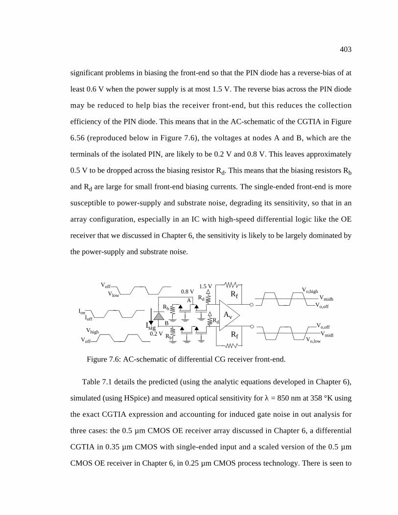
403
significant problems in biasing the front-end so that the PIN diode has a reverse-bias of at
least 0.6 V when the power supply is at most 1.5 V. The reverse bias across the PIN diode
may be reduced to help bias the receiver front-end, but this reduces the collection
efficiency of the PIN diode. This means that in the AC-schematic of the CGTIA in Figure
6.56 (reproduced below in Figure 7.6), the voltages at nodes A and B, which are the
terminals of the isolated PIN, are likely to be 0.2 V and 0.8 V. This leaves approximately
0.5 V to be dropped across the biasing resistor Rd. This means that the biasing resistors Rb
and Rd are large for small front-end biasing currents. The single-ended front-end is more
susceptible to power-supply and substrate noise, degrading its sensitivity, so that in an
array configuration, especially in an IC with high-speed differential logic like the OE
receiver that we discussed in Chapter 6, the sensitivity is likely to be largely dominated by
the power-supply and substrate noise.
Table 7.1 details the predicted (using the analytic equations developed in Chapter 6),
simulated (using HSpice) and measured optical sensitivity for λ = 850 nm at 358 °K using
the exact CGTIA expression and accounting for induced gate noise in out analysis for
three cases: the 0.5 µm CMOS OE receiver array discussed in Chapter 6, a differential
CGTIA in 0.35 µm CMOS with single-ended input and a scaled version of the 0.5 µm
CMOS OE receiver in Chapter 6, in 0.25 µm CMOS process technology. There is seen to
Figure 7.6: AC-schematic of differential CG receiver front-end.
Rf
AvIsig
Rf
Vo,off
Vo,high
Vo,off
Vo,low
Vmidh
VmidlVoff
Vhigh
Voff
Vlow
IonIoff
Rd
Rd
Rb
Rb
A
B
0.8 V
0.2 V
1.5 V

404
be reasonable agreement between the measured optical sensitivity at the bandwidth of the
receiver and the simulated/predicted values.
We note that the OE receiver sensitivity obtained from our calculations for the 0.5 µm
CMOS process is approximately -22 dBm (-19 dbm) for λ = 850 nm at 358 °K with Γ=2.5,
using the exact CGTIA (approximate CGTIA) noise expression. We measured -17 dBm
electrical sensitivity (-14 dBm optical) for the 1.1 GHz -3 dB bandwidth receiver array at
2.5 Gb/s. The measured and simulated sensitivity is in good agreement at the bandwidth of
the 0.5 µm CMOS OE receiver array that we have tested. Assuming a worst-case error of
4 dBm (which accounts for increased gate noise, noise contributions from bias circuitry,
second-stage noise contributions, and additional noise terms from differential circuit
components), the optical sensitivity of the 0.1 µm CMOS receiver with 8 GHz bandwidth
is likely to be between -15 dBm and -13 dBm, depending on the value of the front-end
biasing resistors. This has the further assumption that the optical devices do not add noise
to further degrade the receiver sensitivity. Reducing Cd from 300 fF to 100 fF will
improve the optical sensitivity by approximately 2 dBm. Therefore, we believe that an OE
receiver array in 0.1 µm CMOS process technology can achieve a data rate of 10.3125
Gb/s/channel if the sensitivity requirements are relaxed to about -13 dBm.
CMOS Feature
Size (µm)
Predicted (dBm)
Simulated (dBm)
Measured (dBm)
BW (GHz)
Error-Free Data Rate
(Gb/s)
0.5 -22 -16.9 -16.89 1.1 1.5
0.35 -19.5 -18.55 -16.04 1.8 2.0
0.25 -19 -20.2 -15.83 1.9 2.5
Table 7.1: Simulated and measured sensitivity at error-free data rate corresponding to the
bandwidth of different CMOS OE receiver.

405
The implementation of a 10 Gb/s/channel parallel OE data link in 0.1 µm CMOS can
leverage the present work by addressing the following issues:
• The impact of the threshold voltage and its variation across the IC on three and four
transistor stacks, and the consequent circuit modifications
• Laser driver for 1.5 V supply with current/voltage and temperature control
• Improved OE receiver design to reduce the OE receiver sensitivity penalty due to
biasing requirements
• Possible addition of DLLs with large-loop bandwidth in each receiver channel to
reduce the impact of skew
Based on the work in this dissertation, we anticipate that a 10.3125 Gb/s/channel 12-
channel 4:1 multiplexer array with an integrated x4 PLLFS will consume approximately
2 Watts and that an OE receiver array with 1:4 demultiplexer will consume approximately
1.2 Watts, in 0.1 µm CMOS process technology, from a 1.5 V power supply. The link can
also be implemented as a 11-channel parallel data link, with clock and frame combined
into one channel. This solution benefits from lower skew in the fiber, but has the
complexity- and power-penalty of a PLL in the OE receiver IC in order to separate the
clock and frame signals.
7.1 Link Performance
Toward the goal of integrating OE interface circuitry in CMOS on the same substrate
with circuits implementing complex system functionality, we recall that this dissertation
aims to find the highest link performance parallel data link in CMOS process technology,
where link performance, LP, was defined in Chapter 1, as the ratio of the products of the
form-factor, F, the effective bit-rate per channel, B, and the maximum distance of
transmission, D, to the power consumption per channel, P.

406
In more formal terms,
LP = F * B * D / P = Form factor * Effective bit rate * Distance / Power [Bit / Watt
sec] (7.1)
where form-factor is defined as the number of signal lines/unit length. Crosstalk is implic-
itly accounted for in the form-factor.
The link performance LP for the three cases of coaxial cable, PCB and fiber-optic
ribbon using the OE and electrical 0.5 µm CMOS circuitry that we have demonstrated is
• 550 Tb/(W sec) for an array of 12 CMOS electrical receiver circuits and 12
electrical transmit circuits connected to 38 m of coaxial cable with 2.4 mm diameter
• 53 Tb/(W sec) for an array of 12 electrical receiver and transmit circuits connected
to 0.764 m of 1 mil wide 50 ohm striplines with 0.5 mm pitch
• 9901 Tb/(W sec) for an array of 12 OE receivers and 12 VCSEL drivers connected
to 300 m of mutli-mode fiber-optic ribbon with 3 mm width and 75 ps of skew
Comparing these values, we see that the link performance of the parallel OE data link
is better than interconnections in coaxial cable by a factor of 18 for data rates of 2.5 Gbit/s
and beyond. These favorable cost considerations warrant designers to consider parallel OE
data links for interconnecting boards in racks.
In conclusion, comparing the link performances developed earlier in this section, we
are able to state that the highest link performance data link in CMOS technology is a
parallel OE data link.
7.2 Dissertation Contributions
The contributions of this work are
1. The demonstration of the truth of the hypothesis that the highest link performance
parallel data link in CMOS technology is a parallel OE link.

407
2. The design and test of the components of a functional parallel data link -- N:1/1:N
multiplexer and demultiplexer circuits, electrical transmit and receive circuits, low-
jitter wide-range PLLFS, OE transmit and receive circuits, and the clocking strategy
optimized for the best link performance in 0.5 µm CMOS process technology.
The contributions of this dissertation, all of which have been validated in 0.5 µm
CMOS process technology, and shown extendable to finer feature size CMOS process
technologies are the following:
1. Demonstration of the link components of a 12-channel 2.5 Gb/s/channel parallel OE
and electrical data link.
2. Active Pull Down Level Shift Diode connected Load configuration which enables
differential logic cells, flip-flops, and amplifiers with higher bandwidth due to lower
parasitics at the output for the same bias currents as conventional load devices.
3. A circuit technique for reducing the jitter in a wide-range ring oscillator based VCO,
based on the concept of changing the VCO gain and frequency range of operation.
This includes the validation of a wide-range delay cell which is used in the VCO and
delay chains.
4. High-speed low-jitter clocking strategies for high-speed parallel OE and electrical
data links.
5. A high-speed CMOS logic style which enables low-power low-skew clock
distribution.
6. Low-power high-speed receiver and transmitter circuits for parallel electrical links.
7. Low-power high-speed direct VCSEL driver circuit.

408
8. Circuit techniques to achieve low-power, high sensitivity, high bit-rate OE receiver
arrays with integrated high-speed logic circuitry and clock distribution circuitry.
7.3 Future Work
Techniques such as IQ modulation, Pulse Amplitude Modulation (PAM), Quadrature
Amplitude Modulation (QAM), multilevel signaling etc., can be used to increase the data
rates over electrical interconnect. Their advantage is that the bandwidth requirements are
lower than that for solutions that signal at the true data rate. Multilevel signaling, which
has been used for implementing modems in the past, has been proposed for increasing data
rates over electrical interconnect [214] and optical data transmission [215]. It is not clear
at this time what the linearity requirements of lasers are, in order to take implement
multilevel coding. It is also not clear how multilevel coding will impact the sensitivity of
the receiver. In order to remain competitive with all-electrical data links in CMOS process
technology, and enable low-cost parallel OE data links in CMOS process technology, the
combination of multilevel coding and/or IQ modulation techniques, and WDM, in the
context of parallel OE data links, is a very attractive area for further research.
7.4 Conclusions
The intimate integration of optics and CMOS is quite feasible as shown by this work,
but the depth of insertion of parallel optics into systems will have strong competition from
electronics over short length scales (< 10 m). The eventual system insertion of parallel
optics into systems requires that the path of migration for system and circuit designers be
made easy. This will require broad support in the form of cell libraries, PCB layout, and
innovative packaging. It will also require that the performance improvement of CMOS
parallel OE data links be maintained over CMOS electrical interconnect solutions. This
requires innovative circuit and system design, which are needed to enable the intimate

409
integration of optics and CMOS. This needs appropriate packaging and device support
such as isolated PIN diodes and high-efficiency, high-bandwidth, low capacitance PIN
diodes.

410
References
[1] The Intel Museum Web page, http://www.intel.com/intel/museum/25anniv/hof/moore.htm.
[2] Taur, Y., Mii, Y.-J., Wong, H.-S., Buchanan, D. A., Wind, S. J., Rishton,S. A., Sai-Halasz, G. A., and Nowak, E. J., ‘CMOS scaling into the 21stcentury: 0.1 µm and beyond,’ IBM Journal of Research and Development,39, No. 12, 1995, pp 245-260.
[3] Iwai, H., ‘CMOS Technology -- Year 2010 and Beyond,’ IEEE Journal ofSolid State Circuits, Vol. 34, No. 3, pp 357-366, March 1999.
[4] The Semiconductor Industry Association 1997 Roadmap, http://www.itrs.net/ntrs/publntrs.nsf.
[5] Nordin, R. A., Levi, A. F. J., Nottenburg, R. N., O'Gorman, J., Tanbun-Ek, T., and Logan, R. A., ‘A systems perspective on digital interconnec-tion technology,’ J. Lightwave Technol., 1992, 10, pp. 811-827.
[6] Krishnamoorthy, A. V., Miller and D. A. B., ‘Scaling Optoelectronic-VLSI Circuits into the 21st Century: A Technology Roadmap,’ IEEEJournal of Selected Topics in Quantum Electronics, 1996, 2, pp 55 - 76.
[7] Kanjamala, A. P. and Levi, A. F. J., ‘Subpicosecond skew in multimodefibre ribbon for synchronous data transmission,’ Electronics Letters,1995, 31 (16), pp 1376-1377.
[8] Bakoglu, H. B., ‘Circuits, Interconnections and Packaging for VLSI,’ Ad-dison Wesley, Reading, 1990.
[9] Sano, B., Madhavan, B., and Levi, A. F. J., ‘8 Gbps CMOS interface forparallel fiber-optic links,’ Electron. Lett., 1996, 32, pp. 2262-2263.
[10] Yang, K. C. and Horowitz, M. A., ‘A 0.8 µm CMOS 2.5 Gb/s Oversam-pling Receiver and Transmitter for Serial Links,’ IEEE Journal of SolidState Circuits, 1996, 31, pp 2015 - 2023.

411
[11] Dally, W. and Poulton, J., ‘Transmitter Equalization for 4Gb/s Signal-ling,’ Proc. of Hot Interconnects, Stanford University, Palo Alto, August15-17, 1996, pp 29-39.
[12] Poulton, J., Dally, W. and Tell, S., ‘A Tracking Clock Recovery Receiverfor 4Gb/s Signaling,’ Proc. of Hot Interconnects, Stanford University,Palo Alto, August 21-24, 1997, pp 157-169.
[13] Levi, A. F. J., ‘Optical Interconnects in Systems,’ Proceedings of theIEEE, June 2000.
[14] Fiedler, A., MacTaggart, R., Welch and J., Krishnan, S., ‘A 1.0625 Gbit/s Transceiver with 2x-Oversampling and Transmit Signal Pre-Emphasis,’IEEE International Sold State Circuits Conference, San Francisco, Cali-fornia, 1997, pp 238-239.
[15] ‘IEEE Standard for scalable coherent interface (SCI)’ (IEEE, New York,1992), IEEE Std 1596-1992.
[16] ‘High-performance parallel interface - 6400 Mbit/s physical layer (HIPPI-6400-PH),’ Tech. Committee of Accredited Standards, X3T11, May1996.
[17] HIPPI-6400 Mbit/s Optical Specification (HIPPI-6400-OPT),http://www.hippi.org/c6400OPT.html.
[18] Madhavan, B., and Levi, A. F. J., ‘55 Gbps/cm data bandwidth density in-terface in 0.5 mm CMOS for advanced parallel optical interconnects,’Electron. Lett., 1998, 34, pp. 1846-1847.
[19] Hahn, K., Kirk, K. S., Wilson, R. E., Straznicky, J., Wong, E. G., Tan, M.R., Kaneshiro, K. T., Dolfi, D. W., Mueller, E. H., Plotts, A. E., Murray.D. D., Marchegiano, J. E., Booth, B. L., Sano, B. J., Madhavan, B., Ragha-van, B., and Levi, A. F. J., ‘Gigabyte/s Data Communications with POLOParallel Optical Link,’ The 46th Electronics Components and TechnologyConference, Orlando, Florida, May 28-31, 1996, pp. 301-307 (IEEE cat#96CH35931).
[20] ‘Draft Standard for Low-Voltage Differential Signals (LVDS) for Scal-able Coherent Interface (SCI)’ (IEEE, New York, 1992), Draft 1.26 IEEEP1596.3-1995.
[21] Yang, G. M., MacDougal, M. H. and Dapkus, P. D., ‘Ultralow ThresholdVertical Cavity Surface Emitting Lasers Obtained with Selective Oxida-tion,’ Electronics Letters, 1995, 31, pp 886-888.

412
[22] Deppe, D. G., Huffaker, D. L., Deng, H. Y., Deng, Q. and OH, T. H., ‘Ul-tra-low threshold Current Vertical Cavity Surface Emitting Lasers forPhotonic Integrated Circuits,’ IEICE Transactions on Electronics, 1997,E80C, pp 664-674.
[23] Sexton, M. et al., ‘Transmission Networking: SONET and the Synchro-nous Digital Hierarchy,” Artech House, Boston, 1992.
[24] Nowell, M. and Nicholl, G., ‘Low Cost OC-192 Interface based on Paral-lel Optics,’ OIF, Los Angeles, 1999.
[25] Yoon, T. and Jalali, B., ‘1 Gbit/s fibre channel CMOS transimpedanceamplifier,’ Electronics Letters, 1997, 33, pp 588-589.
[26] Yoon, T. and Jalali, B., ‘1.25 Gbit/s CMOS Differential TransimpedanceAmplifier for Gigabit Networks,’ Proceedings of the 23rd European Sol-id-State Circuits Conference, Southampton, UK,16-18 September 1997,pp 140-143.
[27] Hu, C., ‘Future CMOS Scaling and Reliability,’ Proceedings of the IEEE,81, No 5, May 1993, pp 682-689.
[28] Lee, K., Kim, S., Ahn, G., and Jeong, D., ‘A CMOS serial link for fullyduplexes data communication,’ IEEE Journal of Solid State Circuits,1995, Vol. 30, No. 4, pp 353-364.
[29] Marbot, R., Cofler, A., Lebihan, J., Nezamzadeh, R., ‘Integration of mul-tiple bidirectional point-to-point serial links in the gigabits per secondrange,’ Unpublished manuscript, BULL Serial Link Technology.
[30] Cecchi, D., Dina, M., and Preuss. C., ‘A 1.0 Gbps SCI link in 0.8 µm BiC-MOS,’ Unpublished manuscript, IBM Corporation, System Technologyand Architecture Division, Rochester, MN.
[31] Ware, K. M., Lee H. and Sodini, C.G., ‘A 200-MHz CMOS phase-lockedloop with dual phase detectors,’ IEEE Journal of Solid State Circuits,1989, Vol. 24, No. 6, pp 1560-1568.
[32] Ng, K. K., and Lynch, W. T., ‘Analysis of the Gate-Voltage-DependentSeries Resistance of MOSFETs,’ IEEE Transactions On Electron Devic-es, Vol ED-33, No. 7, July 1986, pp 965-972.
[33] Ng, K. K,. and Lynch, W. T., ‘The Impact of Intrinsic Series Resistanceon MOSFET Scaling,’ IEEE Transactions On Electron Devices, Vol ED-34, No. 3, March 1987, pp 503-511.

413
[34] Scott, D. B., Hunter, W. R., and Shichijo, H., ‘A Transmission Line Modelfor Silicided Diffusions: Impact on the Performance of VLSI Circuits,’IEEE Transactions On Electron Devices, Vol ED-29, No 4, April 1982, pp651-661.
[35] Murrmann, H. and Widmann, D., ‘Current crowding on Metal Contacts toPlanar Devices,’ IEEE Transactions On Electron Devices, Vol ED-16, No12, December 1969, pp 1022-1024.
[36] Schulze, K. W., ‘High-Speed Inter-Chip Communication,’ Master’s The-sis, Department of Computer Science, Technical University of Denmark,1995.
[37] Gustavson, D. B., ‘The Scalable Coherent Interface and Related StandardsProjects,’ IEEE Micro, February 1992, pp 10-22.
[38] Gunning, B., Yuan, L., Nguyen, T., and Wong, T. ‘A CMOS Low VoltageSwing Transmission Line Transceiver,’ IEEE International Solid StateCircuits Conference, 1992, pp 58-59.
[39] Brews, J. R., Ng, K. K. and Watts, R. K., ‘The Submicrometer SiliconMOSFET,’ in R. K. Watts (Ed.), ‘Submicron ICs,’ Wiley Interscience,1989.
[40] Walker, R., Wu, J., Stout, C., Lai, B., Yen, C., Hornak, T. and Petruno, P.,‘A 2-Chip 1.5 Gb/s Bus-oriented Serial Link Interface,’ IEEE Internation-al Solid State Circuits Conference Digest of Technical Papers 25 (Febru-ary 19-21 1992), pp 226-227,291.
[41] Smith, R. G. and Personick, S. D., ‘Receiver Design for Optical FiberCommunication Systems,’ Topics in Applied Physics, H. Kressel Editor,Vol 39, Springer Verlag, Berlin, 1980, pp 89-160.
[42] Kim, S., Lee, K., Moon, Y., Jeong, D-K., Choi, Y. and Lim, J. K.,‘A 960Mb/s Interface for skew-Tolerant Bus Using Low Jitter PLL,’ IEEE Jour-nal of Solid State Circuits, Vol. 32, No. 5., May 1997, pp 691-700.
[43] Lee, K., Kim, S., Ahn, G. and Jeong, D-K., ‘A CMOS Serial Link for Ful-ly Duplexed Data Communications,’ IEEE Journal of Solid State Circuits,Vol. 30, No. 4, April 1995, pp 353-364.
[44] Huang., W. M., et al., ‘A high speed bipolar technology featuring self-aligned single poly base and submicrometer emitter contacts,’ IEEE Elec-tron Device Letters, Vol. 11, No 9, pp 412-414, Sep. 1990.

414
[45] ----,‘MC100SX1451 Spanceiver (Serial to Parallel Transceiver),’ Elec-tronics, May 9, 1994.
[46] Sidiropoulos, S. and Horowitz, M., ‘A 700 Mb/s CMOS Signaling Inter-face Using Current Integrating Receivers,’ IEEE Journal of Solid StateCircuits, Vol. 32, No. 5, May 1997, pp 681-690.
[47] Carter, R. O, ‘Low-Disparity Binary Coding System,’ Electronics Letters,May 1965, Vol. 1, No. 3, pp 67-68.
[48] Kiwigami, R. K., ‘Encoding/Decoding for Magnetic Record Storage Ap-paratus,’ IBM Technical Disclosure Bulletin, Vol. 18, No. 10, March1976, pp 3147-3149.
[49] Widmer, A. X. and Franaszek, P. A., ‘Transmission code for high-speedfiber optic data networks,’ Electronics Letters, Vol. 19, No. 6, 17 March1983, pp 202-203.
[50] Griffiths, J. M., ‘Binary Code Suitable for Line Transmission,’ Electron-ics Letters, Vol. 5. No. 4, 20th February 1969, pp 79-81.
[51] Widmer, A. X. and Franaszek, P. A., ‘A DC-Balanced, Partitioned-Block,8B/10B Transmission Code,’ IBM Journal of Research and Development,Vol. 27, No. 5, September 1983, pp 440-451.
[52] Thompson, B., Lee, H-S. and DeVito, L. M.,‘A 300 MHz BiCMOS SerialData Transceiver,’ IEEE Journal of Solid State Circuits, Vol. 29, No. 3,March 1994, pp 185-192.
[53] Blood Jr., W. R., ‘MECL System Design Handbook,’ Motorola, HB205,Rev 1, 1988.
[54] Petty, C. and Pearson, T.,‘Designing with PECL,’ Application note AN-1406, ECL Applications Engineering, Motorola.
[55] Hedberg, M. and Haulin, T., ‘I/O Family with 200mV to 500 mW SupplyVoltage,’ IEEE International Solid State Circuits Conference Digest ofTechnical Papers, February 1997, San Francisco, pp 214-215.
[56] C. Calamvokis et al., ‘Afterburner Specification Version 1.0,’ NetworkTechnology Department, Hewlett Packard Laboratories, Bristol England,June 1993.
415
[57] C. Dalton et al., “Afterburner: A network-independent card provides ar-chitectural support for high-performance protocols” IEEE Networks, pp.36-43, July 1993.
[58] A. Edwards et al., “User-space protocols deliver high performance to ap-plications on a low-cost Gb/s LAN,” ACM SIGCOMM, 1994.
[59] C. Maitland, “Standard Graphics Connection Specification,” (A-5960-1585-1), Hewlett-Packard Graphics Division, Rev. 3.0, Nov. 21, 1991.
[60] CCITT, ‘AAL Type 5, Draft Recommendation Text for Section 6 ofI.363’ CCITT Study Group XVIII/8-5, Oct. 1992.
[61] Madhavan, B., Sano, B., Levi, A. F. J., ‘A Novel High Speed Low SkewClock Distribution Scheme in 0.8 Micron CMOS,’ International Sympo-sium on Circuits and Systems, 1996, pp. 149-152.
[62] Personick, S. D., ‘Receiver Design for Digital Fiber Optic Communica-tion Systems I,’ Bell System Technical Journal, Vol. 52, No. 6, July-Au-gust 1973, pp 843-874.
[63] Personick, S. D., ‘Receiver Design for Digital Fiber Optic Communica-tion Systems II,’ Bell System Technical Journal, Vol. 52, No. 6, July-Au-gust 1973, pp 875-886.
[64] Williams, G., ‘Lightwave Receivers,’ Topics in Lightwave Communica-tion, Tingye Li, Editor, Academic Press, San Diego, 1991, pp 79-149.
[65] Liechti, C. A. et al., ‘A GaAs MSI word generator operating at 5 Gbit/sdata rate,’ IEEE transactions on Microwave Theory and Techniques, Vol.MTT-30, pp 998-1006, July 1982.
[66] Takai, A., Kato, S., Yamashita, S., Hanatani, S., Motegi, Y., Ito, K., Abe,H. and Kodera, H., ‘200-Mb/s/ch 100-m Optical Subsystem Interconnec-tions using 8-channel 1.3 µm Laser Diode Arrays and Single-Mode FiberArrays,’ Journal of Lightwave Technology, Vol. 12, No. 2, February1994, pp 260-269.
[67] Lee, T. H. and Bulzacchelli, H. F., ‘A 155 MHz Clock Recovery Delayand Phase-Locked Loop,’ IEEE Journal of Solid State Circuits, Vol. 27,No. 12, December 1993, pp 1736-1746.
[68] Pederson, M., and Metz, P.,‘A CMOS to 100K ECL Interface Circuit,’IEEE International Solid State Circuits Technical Digest of Papers, Feb-ruary 17, 1989, pp 226-227.

416
[69] Steyaert, M. S. J., Bijker, W. and Sevenhans, J., ‘ECL-CMOS and CMOS-ECL Interface in 1.2 µm CMOS for 150 MHz Digital ECL Data transmis-sion Systems,’ IEEE Journal of Solid State Circuits, Vol. 26, No. 1, Janu-ary 1991, pp 18-24.
[70] Ishibe, M., Otaka, S., Takeda, J., Tanaka, S., Toyoshima, Y., Takatsuka,S., Shimizu, S., ‘High-Speed CMOS IO Buffer Circuits,’ IEEE Journal ofSolid State Circuit, Vol. 27, No. 4, April 1992, pp 671-673.
[71] Meier, S. R, Man, E. D., Noll, T. G., Loibl, U. and Klar, H.,‘A 2µmCMOS Digital Adaptive Equalizer Chip for QAM Digital Radio Mo-dems,’ IEEE Journal of Solid State Circuits, Vol. 23, No. 5, October 1988,pp 1212-1217.
[72] Knight, T. F. and Krymm, A., ‘A Self-Terminating Low Voltage SwingCMOS Output Driver,’ IEEE Journal of Solid State Circuits, Vol. 23, No.2, April 1988, pp 457-464.
[73] Schumacher, H-J., Dikken, J., Seevnick, E.,‘CMOS Sub nano-secondTrue-ECL Output Buffer,’ IEEE Journal of Solid State Circuits, Vol. 25,No. 1, February 1990, pp 150-154.
[74] Kawamura, T., Suzuki, M. and Ichino, H., ‘An Extremely Low-power Bi-polar Current-mode I/O Circuit for Multi-Gbit/s Interfaces,’ Symposiumon VLSI Circuits Digest of Technical papers, 1994, pp 31-32.
[75] Murata, K., Otsuji, T., Sano, E., Ohhata, M. and Togashi, M., ‘A NovelHigh-Speed Latching operation Flip-Flop (HLO-FF) Circuit and its appli-cation to a 19-Gb/s Decision Circuit Using a 0.2 µm GaAs MESFET,’IEEE Journal of Solid State Circuits, Vol. 30, No. 10, October 1995, pp1101-1107.
[76] Ohuchi, M. et al., ‘A Si Bipolar 5-Gb/s 8:1 Multiplexer and 4.2 Gb/s 1:8Demultiplexer,’ IEEE Journal of Solid State Circuits, Vol. 27, No. 4, April1992, pp 664-667.
[77] Lao, Z. H., Langmann, U., Albers, J, N., Schlag, E. and Clawin, D., ‘A 12Gb/s Bipolar 4:1 Multiplexer IC for SDH Systems,’ IEEE Journal of SolidState Circuits, VOl. 30, No. 2, February 1995, pp 129-131.
[78] Razavi, B. and Sung, J. M., ‘A 6 GHz 60 mW BiCMOS PLL,’ IEEE Jour-nal of Solid State Circuits, Vol. 29, No. 12, December 1994, pp 1560-1565.

417
[79] Razavi, B., Lee, K. F. and Yan, R. H., ‘Design of High-Speed, Low-PowerFrequency Dividers and Phase-Locked Loops in Deep SubmicronCMOS,’ IEEE Journal of Solid State Circuits, Vol. 30, No. 2, February1995, pp 101-109.
[80] Razavi, B., and Wooley, B., ‘Design Techniques for High-Speed, High-Resolution Comparators,’ IEEE Journal of Solid State Circuits, Vol. 27,No. 12, December 1992, pp 1916-1926.
[81] Razavi, B., Ota, Y. and Swartz, R. G., ‘Design Techniques for Low-Volt-age High-Speed Digital Bipolar Circuits,’ IEEE Journal of Solid State Cir-cuits, Vol. 29, 1994, pp 332-339.
[82] Razavi, B., ‘A Study of Phase Noise in CMOS Oscillators,’ IEEE Journalof Solid State Circuits, Vol 31, No. 3, march 1996, pp 331-343.
[83] Kurisu, M., Uemura, G., Ohuchi, M., Ogawa, C., Takemura, H., Morika-wa, T. and Tashiro, T., ‘A Si Bipolar 28-GHz Dynamic Frequency Divid-er,’ IEEE Journal of Solid State Circuits, Vol. 27, No. 12, December 1992,pp 1799-1804.
[84] Shikata, M., Tanaka, K., Yamada, H. T., Fujishiro, H. I., Nishi, S., Yam-agishi, C. and Akiyama, N., ‘A 20-Gb/s Flip-Flop Circuit Using Direct-Coupled FET Logic,’ IEEE Journal of Solid State Circuits, Vol. 28, No.10, October 1993, pp 1046-1052.
[85] Kuroda, T., Fujita, T., Itabashi, Y., Kabumoto, S., Noda, M. and KanumaA., ‘1.65 Gb/s 60 mW 4:1 Multiplexer and 1.8 Gb/s 80 mW 1:4 Demulti-plexer ICs using 2V 3-Level Series-Gating ECL Circuits,’ IEEE Interna-tional Solid State Circuits Conference Digest of Technical Papers, 1995,pp 36-37.
[86] Oshima, Y., Yoshinaga, K., Yamaguchi, S., Morita, T., Morisaki, S,Kawana, M. and Kodachi, T., ‘A Single CMOS SDH Termination Chipfor 622 Mb/s STM-4C,’ IEEE International Solid State Circuits Confer-ence Digest of Technical Papers, 1994, pp 174-175.
[87] Andersson, L. I., Rudberg, B. G. R., Lewin, T. P., Reed, M. D., Planer, S.M. and Sundaram, S. L., ‘Silicon Bipolar Chipset for SONET/SDH 10 Gb/s Fiber-Optic Communication Links,’ IEEE Journal of Solid State Cir-cuits, Vol. 30, No. 3, March 1995, pp 210-218.
[88] Yuan, J. and Svensson, C., ‘High-Speed CMOS circuit technique,’ IEEEJournal of Solid State Circuits, Vol. 24, No. 1, Feb 1989, pp 62-71.

418
[89] Yuan, J. and Svensson, C., ‘New Single-Clock CMOS Latches and Flip-flops with Improved Speed and Power Savings,’ IEEE Journal of SolidState Circuits, Vol. 32, No. 1, January 1997, pp 62-69.
[90] Huang, Q. and Rogenmooser, R., ‘Speed Optimization of Edge-triggeredCMOS Circuits for Gigahertz Single-Phase Clocks,’ IEEE Journal of Sol-id State Circuits, Vol. 31, No. 3, March 1996, pp 456-465.
[91] Blair, G. M., ‘Comment on New Differential Flip-flops from Yuan andSvensson,’ Electronics Letters, Vol. 32, No. 23, 7th November 1996, pp2125-2126.
[92] Larsson, P. and Svensson, C., ‘Impact of Clock Slope on True SinglePhase Clocked (TSPC) CMOS Circuits,’ IEEE Journal of Solid State Cir-cuits, Vol. 29, No. 6, June 1994, pp 723-726.
[93] Larsson, P. and Svensson, C., ‘Noise in Digital Dynamic CMOS Circuits,’IEEE Journal of Solid State Circuits, Vol. 29, No. 6, June 1994, pp 655-662.
[94] Dobberpuhl, D. W., Witek, R. T., Allmon, R., Anglin, R., Bertucci, D.,Britton, S., Chao, L., Conrad, R. A., Dever, D. E., Gieseke, B., Hassoun,S. M. N., Hoeppner, G. W., Kuchler K., Ladd, M., Leary, B. M., Madden,L., McLellan, E. J., Meyer, D. R., Montanaro, J., Priore, D. A., Rajago-palan, V., Samudrala, S. and Santhanam, S., ‘A 200-MHz 64-b Dual-IssueCMOS Microprocessor,’ IEEE Journal of Solid State Circuits, Vol. 27,No. 11, November 1992, pp 1555-1570.
[95] -----,‘High Performance ECL Data ECLinPs and ECLinPs Lite,’ Motoro-la, Inc, DL 140/D Rev 3., 1995.
[96] Wong, Y. M., Muehlner, D. J., Faudskar, C. C., Fishteyn, M., Gates, J. V.,Anthony, P. J., Cyr, G. J., Choi, J., Crow, J. D., Kuchta, D. M., Pepel-jugoski, P. K., Stawiasz, K., Nation, W., Engebretsen, D., Whitlock, B.,Morgan, R. A., Hibbs-Brenner, M. K., Lehman, J., Walterson, R., Kal-weit, E., and Marta, T., ‘OptoElectronic Technology Consortium (OETC)Parallel Optical Data Link: Components, System Applications and Simu-lation Tools,’ The 46th Electronics Components and Technology Confer-ence, Orlando, Florida, May 28-31, 1996, pp. 269-278 (IEEE cat#96CH35931).

419
[97] Crow, J. D., Choi, J., Cohen, M. S., Johnson, G., Kuchta, D., Lacey, D.,Poonapalli, S., Pepeljugoski, P., Stawiasz, K., Trewhella, J., Xiao, P.,Tremblay, S., Ouimet, S., Lacerte, A., Gauvin, M., Booth, D., Nation, W.,Smith, T. L., DeBaun, B. A., Henson, G. D., Igl, S. A., Lee, N. A., Piekarc-zyk, A. J., Kuczma, A. S., Spanoudis, S. L., ‘The Jitney Parallel OpticalInterconnect,’ The 46th Electronics Components and Technology Confer-ence, Orlando, Florida, May 28-31, 1996, pp. 292-300 (IEEE cat#96CH35931).
[98] Swirhun, S., Dudek, M., Neumann, R., Calkins, J., Brusenbach, P., Brink-man, D., Northrop, T., Moore, A., Paananen, D., Scott, J., White, T., ‘TheP-VixeLinkTM Multichannel Optical Interconnect,’ The 46th ElectronicsComponents and Technology Conference, Orlando, Florida, May 28-31,1996, pp. 316-320 (IEEE cat# 96CH35931).
[99] Carson, R. F., Lovejoy, M. L., Lear, K. L., Warren, M. E., Seigal, P. K.,Patrizi, G. A., Kilcoyne, S. P. and Craft, D. C., ‘Low-Power Modular Par-allel Photonic Data Links,’ The 46th Electronics Components and Tech-nology Conference, Orlando, Florida, May 28-31, 1996, pp. 321-326(IEEE cat# 96CH35931).
[100] Madhavan, B. and Levi, A. F. J., ‘Low-Power 2.5 Gigatbit/s 0.5 µmCMOS VCSEL driver,’ Electronics Letters, Vol. 34, 1998, pp 178-179.
[101] Xiao, P., Kuchta, D., Stawiasz, K., Ainspan, H., Choi, J. and Shin, H., ‘A500 Mb/s, 20-channel CMOS Laser Diode Array Driver for a Parallel Op-tical Bus,’ IEEE International Solid State Circuits Conference Digest ofTechnical Papers, Feb 6-8, San Francisco, 1997, pp 250-251.
[102] Umeda, T., Yoshihara, K., Konno, M., Kaminishi, K. and Hiarakawa, K.,‘A 1.4 Gb/s 12-channel Parallel Laser diode driver IC for Optical Inter-connections,’ IEEE International Solid State Circuits Conference Digestof Technical Papers, 1996, pp 292-293, 460.
[103] Schneider Jr., R. P., Tan, M. R. T., Corzine, S. W. and Wang S. Y., ‘Ox-ide-confined 850 nm veritcal-cavity lasers for multimode-fibre data com-munications,’ Electronics Letters, Vol. 32, No. 14, 4th July 1996, pp1300-1302.
[104] Tsay, R-S., ‘Exact Zero Skew,’ IEEE International Conference on Com-puter Aided Design, 1991, pp 336-339.
[105] Shanley, T. and Anderson, D., ‘PCI System Architecture,’ Third edition,Addison-Wesley, 1995.

420
[106] ----, ‘Accelarated Graphics Port Interface Specification,’ Intel Corpora-tion, http://developers.intel.com.
[107] Kobayashi, K. W. and Oki, A. K., ‘A Low Noise Baseband 5-GHz Direct-Coupled HBT Amplifier with Common-Base Active Input Match,’ IEEEMicrowave and Guided Wave Letters, Vol. 4., No. 11, November, 1994,pp 373-375.
[108] Hurm, V., Benz, W., Berroth, M., Bronner, W., Fink, T., Haupt, M.,Kohler, K., Ludwig, M., Raynor, B. and Rosenzweig, J., ‘10 Gbit/s long-wavelength monolithic opto-electronic receiver grown on GaAs,’ Elec-tronics Letters, Vol. 32, No. 4, 15th February 1996, pp 391-392.
[109] Yoneyama, M., Sano, E., Yamahata, S., Matsuoka, Y., and Yaita, M., ‘17Gbit/s pin-PD/decision circuit using InP/InGaAs double-hetero-junctionbipolar transistors,’ Electronics Letters, Vol. 32, No. 4, 15th February1996, pp 393-394.
[110] Scheinberg, N., Bayruns, R. J., and Laverick, T. M., ‘Monolithic GaAstransimpedance Amplifiers for Fiber-Optic Receivers,’ IEEE Journal ofSolid State Circuits, Vol. 26, No. 12, December 1991, pp 1834-1839.
[111] Meyer, R. G. and Mack, W., ‘A Wideband Low-Noise Variable-GainBiCMOS Transimpedance Amplifier,’ IEEE Journal of Solid State Cir-cuits, Vol. 29, No. 6, June 1994, pp 701-706.
[112] Soda, M., Tezuka, H., Sato, F., Hashimoto, T., Nakamura, S., Tatsumi, T.,Suzaki, T. and Tashiro, T., ‘Si-Analog ICs for 20 Gb/s Optical Receiver,’IEEE Jouranl of Solid State Circuits, Vol. 29, No. 12, pp 1577-1582.
[113] Yamashita, K., Kinoshita, T., Takasaki, Y., Maeda, M., Kaji, T. and Mae-da, N., ‘A Variable Transimpedance Preamplifier For Use in Wide Dy-namic Range Optical Receivers,’ IEEE Journal of Solid State Circuits,Vol. 21, No. 2, April 1986, pp 324-329.
[114] Van Den Broeke, L. A. D. and Nieuwkerk, A. J., ‘Wide -Band IntegratedOptical Receiver with Improved Dynamic Range Using a Current Switchat the Input,’ IEEE Journal of Solid State Circuits, Vol. 28, No. 7, July1993, pp 862-864.
[115] Ishihara, N., Fujita, S., Togashi, M., Hino, S., Arai, Y., Tanaka, N., Koba-yashi, Y. and Akazawa, Y., ‘3.5-Gb/s x 4-Ch Si bipolar LSIs for OpticalInterconnections,’ IEEE Journal of Solid State Circuits, Vol. 30, No. 12,December 1995, pp 1493-1501.

421
[116] Moller, M., Rein, H. -M. and Wernz, H., ‘13 Gb/s Si-Bipolar AGC Am-plifier IC with High Gain and Wide Dynamic Range for Optical-Fiber Re-ceivers,’ IEEE Journal of Solid State Circuits, Vol. 29, No. 7, July 1994,pp 815-822.
[117] Neuhauser, M., Rein, H. -M. and Wernz, H., ‘Low-Noise, High-Gain, Si-Bipolar Preamplifiers for 10 Gb/s Optical-Fiber Links -- Design and Re-alization,’ IEEE Journal of Solid State Circuits, Vol. 31, No. 1, January1996, pp 24-29.
[118] Neuhauser, M., Rein, H. -M.,Wernz, H. and Felder, A., ‘13 Gb/s Si Bipo-lar Preamplifier for Optical Front Ends,’ IEEE Journal of Solid State Cir-cuits, Vol. 31, No. 1, January 1996, pp 24-29.
[119] Suzaki, T., Soda, M., Morikawa, T., Tezuka, H., Ogawa, C., Fujita, S.,Takemura, H. and Tashiro, T., ‘Si Bipolar Chip Set for 10-Gb/s OpticalReceiver,’ IEEE Journal of Solid State Circuits, Vol. 27, No. 12, Decem-ber 1992, pp 1781-1786.
[120] Ramakrishnan, V., Albers, J. N., Nottenburg, R. N. and Hillery, W. J., ‘2.5Gb/s DC Coupled Retimed Optical Transducer with a Dynamic ReferenceVoltage Comparator,’ IEEE Photonics Technology Letters, Vol. 8, No. 5,May 1996, pp 685-687.
[121] Ramakrishnan, V., Albers, J. N., Nottenburg, R. N. and Hillery, W.J.,‘Broadband single-ended to differential signal converter embedded insilicon decision circuit,’ Electronics Letters, Vol. 31, No. 17, 17th August1995, pp 1400-1401.
[122] Ramakrishnan, V., Albers, J. N., Nottenburg, R. N. and Hillery, W.J.,‘Monolithic Retimed Receiver Array with Dynamic Reference LevelComparator for 4x2 Gb/s Synchronous Optical Data Link,’ IEEE Photon-ics Technology Letters, Vol. 9, No. 1, January 1997, pp 82-84.
[123] Ayadi, K., Kuijk, M., Heremans, P., Bickel, G., Borghs and Vounckx, R.,‘A Monolithic Optoelectronics Receiver in Standard 0.7 um CMOS oper-ating at 180 MHz and 176-fJ of Light Input Energy,’ IEEE PhotonicsTechnology Letters, Vol. 9, No. 1, January 1997, pp 88-90.

422
[124] Woodward, T. K., Krishnamoorthy, A. V., Goossen, K. W., Walker, J. A.,Lentine, L. A., Novotny, R. A., D’Asaro, L. A., Chirovsky, L. M. F., Hui,S. P., Tseng, B., Kossives, D., Dahringer, D., Leienguth, R. E., Cunning-ham, J. E., Jan, W. Y. and Miller, D. A. B.,‘15 µm Solder Bonding ofGaAs/AlGaAs MQW Devices to MOSIS 0.8 µm CMOS for 1Gb/s Two-beam Smart-Pixel Receiver/Transmitter,’ IEEE International Solid StateCircuits Conference Digest of Technical Papers, 1996, pp 406-407, 482.
[125] Krishnamoorthy, A. V., Woodward, T. K., Goossen, K. W., Walker, J.A.,Lentine, L. A., Chirovsky, L. M. F., Hui, S. P., Tseng, Leienguth, R.E., Cunningham, J. E. and Jan, W. Y., ‘Operation of single-ended 550Mbit/s, 41fJ, hybrid CMOS/MQW receiver/transmitter,’ Electronics Let-ters, Vol. 32, No. 8, 11th April 1996, pp 764-765.
[126] Ingels, M., Van der Plas, Geert, Crols, J and Steyaert, M., ‘A CMOS 18THzΩ 240 Mb/s Transimpedance Amplifier and 155 Mb/s LED-Driverfor Low Cost Optical Fiber Links,’ IEEE Journal of Solid State Circuits,Vol. 29, No. 12, December 1992, pp 1552-1559.
[127] Nakamura, M., Ishihara, N., Akazawa, Y. and Kimura, H., ‘An instanta-neous response CMOS optical receiver IC with Wide Dynamic Range andExtremely High sensitivity Using Feed Forward Auto-Bias Adjustment,’IEEE Journal of Solid State Circuits, Vol. 30, No. 9, September 1995, pp991-997.
[128] Abidi, A., ‘Gigahertz Transresistance Amplifiers in Fine Line NMOS,’IEEE Journal of Solid State Circuits, Vol. 19, No. 6, December 1984, pp986-994.
[129] Vanisri, T. and Toumazou, C., ‘Integrated High Frequency Low-NoiseCurrent-Mode Optical Transimpedance Preamplifiers: Theory and Prac-tice,’ IEEE Journal of Solid State Circuits, Vol. 30, No. 6, June 1995, pp677-685.
[130] Toumazou, C. and Park, S. M., ‘Wideband Low Noise CMOS Transim-pedance Amplifier for gigaHertz operation,’ Electronics Letters, Vol. 32,No. 13, 20th June 1996, pp 1194-1195.
[131] Van Blerkom, D. A., Fan, C., Blume, M. and Esener, S. C., ‘Transimped-ance Receiver Design Optimization for Smart Pixel Arrays,’ IEEE Journalof Lightwave Technology, to appear in December 1997.
[132] Madhavan, B., Koh, Y. and Levi, A. F. J., ‘800 MHz PECL ReceiveTransmit Circuits in 0.8 µm CMOS,’ unpublished, 1995.

423
[133] Wolaver, D. H.,‘Phase Locked Loop Circuit Design,’ Prentice Hall, En-glewood Cliffs, New Jersey, 1991.
[134] Crawford, F. A., ‘Frequency Synthesizer Design,’ Artech House.
[135] Razavi, B. (Ed.), ‘Monolithic Phase Locked Loops and Clock RecoveryCircuits,’ IEEE Press, 1996.
[136] Rofouragan, A., Rael J., Rofouragan, M. and Abidi, A., ‘A 900 MHzCMOS LC-Oscillator with Quadrature Outputs,’ IEEE International SolidState Circuits Conference Digest of Technical Papers, 1996, pp 392-393.
[137] Soyeur, M., Jenkins, K. A., Bughartz, J. N. and Hulvey, M. D., ‘A 900MHz CMOS LC-Oscillator with Quadrature Outputs,’ IEEE InternationalSolid State Circuits Conference Digest of Technical Papers, 1996, pp 394-395.
[138] Craninckx, J. and Steyaert, ‘A 1.8 GHz Low-Phase Noise CMOS VCOUsing Optimized Hollow Spiral Inductors,’ IEEE Journal of Solid StateCircuits, Vol. 32, April 1996.
[139] Sarpeshkar, R., Delbruck, T., and Mead, C. A., ‘White Noise in MOSTransistors and Resistors,’ IEEE Circuits and Devices, Vol. 9, No. 6, , No-vember 1993, pp 23-29.
[140] Lin, P-S., and Zukowski, C. A., ‘Jitter Due to Signal History in DigitalLogic Circuits and its Control Strategies,’ Proceedings of the IEEE SolidState Circuits and Systems Conference, 1993, pp 2114-2117.
[141] Martin, M., ‘RF Sidebands caused by DC Power Line Fluctuations,’ Mi-crowave Journal, September 1991, pp 166-170.
[142] Gabara, T, ‘Reduced Ground Bounce and Improved Latch-Up Suppres-sion through Substrate Conduction,’ IEEE Journal of Solid-State Circuits,Vol. 23, No. 5, October 1988, pp 1224-1232.
[143] Syed, K. E. and Abidi, A., ‘Gigahertz Voltage-Controlled Ring Oscilla-tor,’ Electronics Letters, Vol. 22, No. 12, 5th June 1986, pp 11-13.
[144] McNeil, J., Croughwell, R., DeVito, L. and Gusinov, A., ‘A 150mW, 155MHz Phase Locked Loop with Low Jitter VCO,’ Proceedings of the Inter-national Solid State Circuits and Systems Conference, 1994, pp 49-52.

424
[145] Banu, M. and Tsividis, Y., ‘Floating Voltage-Controlled Resistors inCMOS Technology”, Electronics Letters, Vol. 18, No. 15, 22nd July1982, pp 678-679.
[146] Wang, Z. and Guggenbuhl, W., ‘A Voltage-Controlled Linear MOSTransconductor Using Bias Offset Technique,’ IEEE Journal of Solid-State Circuits, Vol. 25, No. 1, February 1990, pp 315-317.
[147] Huang, S-C. and Ismail, M.,‘Linear Tunable COMFET Transconductor,’Electronics Letters, Vol. 29, No. 5, 4th March 1993, pp 459-460.
[148] Huang, S-C.,‘Design Of Low-Voltage Linear Tunable CMOS V-I con-verters with a rail-to-rail input range,’ Proceedings of the InternationalSolid State Circuits and Systems Conference, 1996.
[149] Pottbacker, A., Langmann, U. and Schreiber, H-U., ‘A Si Bipolar Phaseand Frequency Detector IC for Clock Extraction up to 8 Gb/s,’ IEEE Jour-nal of Solid-State Circuits, Vol. 27, No. 12, December 1992, pp 1747-1751.
[150] Ebenhoech, H., ‘Make IC digital frequency comparators,’ Electronic De-sign, Vol. 14, July 5, 1967, pp 62-64.
[151] Soyeur, M. and Meyer, R. G., ‘Frequency Limitations of a ConventionalPhase-Frequency Detector,’ IEEE Journal of Solid-State Circuits, Vol. 25,No. 4, August 1990, pp 1019-1022.
[152] Shahriary, I., Brisay, G. D., Avery, S. and Gibson, P., ‘GaAs MonolithicDigital Phase/Frequency Discriminator,’ IEEE GaAs IC Symposium Di-gest of Technical Papers, October 1985, pp 183-186.
[153] Notani, H., et. al., ‘A 622 MHz CMOS phase-locked loop with pre-chargetype phase frequency detector,’ Proceedings of the Symposium on VLSICircuits, June 1994, pp 129-130.
[154] Mijuskovic, D., Bayer, M., Chomicz, T., Garg, N., James, F., McEntarfer,P., and Porter, J., ‘Cell-Based Fully Integrated CMOS Frequency Synthe-sizers,’ IEEE Journal of Solid-State Circuits, Vol. 29, No. 3, March 1994,pp 271-279.
[155] Novof, I., Austin, J., Kelkar, R. Strayer, D. and Wyatt, S., ‘Fully Integrat-ed CMOS Phase-Locked Loop with 15 to 240 MHz Locking Range and+/- 50 ps jitter,’ IEEE International Solid State Circuits Conference Digestof Technical Papers, 1995, pp 112-113.

425
[156] Razavi, B., ‘Principles of Data Conversion System Design,’ IEEE Press,1995.
[157] -----, ‘AD9901: Ultrahigh Speed Phase/Frequency Discriminator,’ Ana-log Devices, 1996.
[158] Hill, A. and Surber, J., ‘The PLL Dead Zone and How to Avoid it,’ RF De-sign, pp 131-134, March 1996.
[159] Larsson, P., ‘High-Speed Architecture for a Programmable Frequency Di-vider and a Dual-Modulus Prescaler,’ IEEE Journal of Solid-State Cir-cuits, Vol. 31, No. 5, May 1996, pp 744-748.
[160] Craninckx, J. and Steyaert, M. S., ‘A 1.75 GHz/3-V Dual-Modulus Di-vide-by-128/129 Prescaler in 0.7 µm CMOS,’ IEEE Journal of Solid-StateCircuits, Vol. 31, No. 7, July 1996, pp 890-897.
[161] Chang, B., Park, J. and Kim, W., ‘A 1.2 GHz CMOS Dual-Modulus Pres-caler Using New Dynamic D-Type Flip-Flops,’ IEEE Journal of Solid-State Circuits, Vol. 31, No. 5, May 1996, pp 749-752.
[162] Seneff, T., McKay, L., Sakamoto, K. and Tracht, N., ‘A Sub-1mA 1.5GHz Silicon Bipolar Dual Modulus Prescaler,’ IEEE Journal of Solid-State Circuits, Vol. 29, No. 10, October 1994, pp 1206-1211.
[163] Aytur, T., and Razavi, B., ‘A 2-GHz, 6-mW BiCMOS Frequency Synthe-sizer,’ IEEE Journal of Solid-State Circuits, Vol. 30, No. 12, December1995, pp 1457-1462.
[164] Bomford, M., ‘Selection of Frequency Dividers for Microwave PLL Ap-plications,’ Microwave Journal, November 1990, pp 159-167.
[165] Borras, J. A., ‘GaAs Phase Noise Characteristics in High Frequency Syn-thesizer Prescalers,’ GaAs IC Symposium, pp 285-286.
[166] Walls, F. L., ‘Low Noise Frequency Synthesis,’ 41st Annual FrequencyControl Symposium, 1987, pp 512-518.
[167] McCLure, M. R., ‘Residual Phase Noise of Digital Frequency Dividers,’Microwave Journal, March 1992, pp 124-130.
[168] Phillip, D. E., ‘Random Noise in Digital Gates and Dividers,’ 41st AnnualFrequency Control Symposium, 1987, pp 507-511.

426
[169] Bomford, M., ‘Analog Division Reduces Noise in PLL Systems,’ Micro-waves & RF, April 1989, pp 98-110.
[170] Robins, W. P., ‘Phase Noise in Signal Sources,’ Peter Peregrinus Ltd.,London, 1982.
[171] Kroupa, V., ‘Noise properties of PLL Systems,’ IEEE Transactions onCommunications, Vol. COM-30, No. 10, October 1982, pp 2244-2252.
[172] Nayebi, M. and Wooley, B., ‘A 10-Bit Video BiCMOS Track-and-HoldAmplifier,’ IEEE Journal of Solid-State Circuits, Vol. 25, No. 12, Decem-ber 1989, pp 1507-1516.
[173] Orguey, H and Vittoz, E., ‘CODYMOS frequency dividers achieve lowpower consumption and high frequency’. Electronics Letters, pp 386-387,August 23, 1973.
[174] Edson, W. A., ‘Noise in Oscillators,’ Proceedings of the IRE, pp 1454-1466, August, 1960.
[175] Lindsey, W. C. and Chie, C. M., ‘Theory of Oscillator instability basedupon structure functions,’ Proceedings of the IEEE, Vol. 64, No. 12, pp1652-1666, December 1976.
[176] ----,‘CSA 803A Communications Signal Analyzer User Manual,’ Tek-tronix, Inc, 1993.
[177] Von der Linde, D., ‘Characterization of the Noise in Continuously Oper-ating Mode-Locked Lasers,’ Applied Physics, Vol. B 39, pp 201-217,1986.
[178] Banu, M., ‘MOS Oscillators with Multi-Decade Tuning Range and Giga-hertz Maximum Speed,’ IEEE Journal of Solid-State Circuits, Vol. 23,No. 4, April 1988, pp 474-479.
[179] Jeong, D-Y, Chai, S-H., Song, W-C. and Cho, G-H., ‘CMOS Current-Controlled Oscillators using Multiple-Feedback Loop Ring Architec-tures,’ IEEE International Solid State Circuits Conference Digest of Tech-nical Papers, February 1997, pp 386-387, pp 401.
[180] Weigandt, T. C., Kim, D. and Gray, P. R., ‘Analysis of Timing Jitter inCMOS Ring Oscillators,’ Proceedings of the IEEE International SolidState Circuits and Systems Conference, 1994, pp 27-30.

427
[181] McNeil, J. A., ‘Jitter in Ring Oscillators,’ IEEE Journal of Solid-State Cir-cuits, Vol. 32, No. 6, June 1997, pp 870-879.
[182] Kih, J., Chang, B., Jeong, D. K. and Kim, W., ‘Class-AB Large-SwingCMOS Buffer Amplifier with Controlled Bias Current,’ IEEE Journal ofSolid-State Circuits, Vol. 28, No. 12, December 1993, pp 1350-1353.
[183] van der Ziel, A., ‘Noise in Solid-State Devices and Lasers,’ Proceedingsof the IEEE, Vol. 58, pp 1178-1206, August 1970.
[184] van der Ziel, A.,‘Gate Noise in Field Effect Transistors at ModeratelyHigh Frequencies,’ Proceedings of the IEEE, Vol. 581, pp 461-467,March 1963.
[185] Shaeffer, D. and Lee, T. H., ‘A 1.5V, 1.5 GHz CMOS Low Noise Ampli-fier,’ IEEE Journal of Solid-State Circuits, Vol. 32, No. 5, May 1997, pp745-759.
[186] Abidi, A. A., ‘High-Frequency Noise Measurements on FETs with SmallDimensions,’ IEEE Transactions of Electron Devices, Vol. ED-33, No.11, November 1986, pp 1801-1805.
[187] Jindal, R. P., ‘Distributed Substrate Resistance Noise in Fine-Line NMOSField-Effect Transistors,’ IEEE Transactions of Electron Devices, Vol.ED-32, No. 11, November 1985, pp 2450-2453.
[188] Jindal, R. P., ‘Distributed Substrate Resistance Noise in Fine-Line NMOSField-Effect Transistors,’ IEEE Transactions of Electron Devices, Vol.ED-31, No. 10, October 1985, pp 1505-1509.
[189] Razavi, B., Yan, R-H. and Lee, K. F., ‘Impact of Distributed Gate Resis-tance on the performance of MOS Devices,’ IEEE Transactions on Cir-cuits and Systems -I: Fundamental Theory and Applications, Vol. 41, No,11, November 1994, pp 750-754.
[190] Rodwell, M. A., ‘ECE594F Class Notes,’ UCSB, unpublished.
[191] Raghavan, B. and Levi, A. F. J., ‘Frequency Response of Copper Intercon-nect,’ unpublished.
[192] Abidi, A. A., ‘On the Noise Optimum of Gigahertz FET TransimpedanceAmplifiers,’ IEEE Journal of Solid State Circuits, Vol. SC-22, No. 6, De-cember 1987, pp 1207-1209.

428
[193] Scheinberg, N., Bayruns, R. J. and Laverick, T. M., ‘Monlithic GaAsTransimpedance Amplifiers for Fiber-Optic Receivers,’ IEEE Journal ofSolid State Circuits, Vol. SC-26, No. 12, December 1991, pp 1834-1839.
[194] Morikuni, J. J. and Kang, S., ‘An Aanlysis of Inductive Peaking in Photo-receiver Design,’ Journal of Lightwave Technology, Vol. 10, No. 10, Oc-tober 1992, pp 1426-1437.
[195] Toumazou, C. and Park, S. M.,‘Wideband Low Noise CMOS Transim-pedance Amplifier for Giga Hertz Operation,’ Electronics Letters, 1996,Vol. 32, No. 13, pp 1194-1196.
[196] Voo. T. and Toumazou, C., ‘High-speed current mirror resistive compen-sation technique,’ Electronics Letters, 1995, Vol. 31, No. 4, pp 248-250.
[197] Zhou, J. and Allstot, D., ‘A Fully Integrated CMOS 900 MHz LNA utiliz-ing Monolithic transformers,’ IEEE International Solid State CircuitsConference, Vol. 41, February 1998, pp 132-133.
[198] Selmi, L., Estreich, D. B. and Ricco, B., ‘Small Signal MMIC Amplifierswith Bridged T-Coil MAtching Networks,’ IEEE Journal of Solid StateCircuits, Vol. SC-27, No. 7, July 1992, pp 1093-1096.
[199] Walls, L., ‘PERL -- A Practical Extraction and Report Language,’ http://www.perl.com.
[200] Sondeen, J., ‘spiral.p -- A perl script to generate coupled planar transform-ers for magic’.
[201] DEC Western Research Laboratories, ‘Magic -- A VLSI Layout System,’http://www.research.digital.com/wrl/projects/magic/magic.html.
[202] Yue, C. P. and Wong, S. S., ‘On-Chip Spiral Inductors with PatternedGround Shields for Si-Based RF ICs,’ IEEE Journal of Solid State Cir-cuits, Vol. SC-33, No. 5, May 1998, pp 743-752.
[203] Kamon, M., Tsulk, M. J. and White, J. K., ‘FASTHENRY: A MultipoleAccelarated 3-D inductance extraction program,’ IEEE Transactions onMicrowave Theory and Techniques, Vol. 42, No. 9, pp 1750-57, Septem-ber 1994.
[204] Avant!, ‘HSpice Manual,’ 1998.

429
[205] Choma, J., ‘Simplified Design Guidelines for Dominant Pole AmplifiersPeaked Actively by Emitter or Source Followers,’ IEEE Transactions onCircuits and Systems, Vol. 36, No. 7, July 1989, pp 1005-1010.
[206] Lee, T., Donnelly, K., Ho, J. T. C., Zerbe, J., Johnson, M. G. and Ishikawa,T., ‘A 2.5 V CMOS Delay Locked Loop for an 18 Mbit, 500 Mbyte/sDRAM,’ IEEE Journal of Solid State Circuits, Vol. SC-29, No. 12, De-cember 1994, pp 1491-1496.
[207] Geiger, R. L., Allen, P. E. and Strader, N. R., ‘VLSI Design Techniquesfor Analog and Digital Circuits,’ McGraw Hill, New York, 1990.
[208] Sackinger, E. and Guggenbuhl, W., ‘A High-Swing, High-ImpedanceMOS Cascode Circuit,’ IEEE Journal of Solid State Circuits, Vol. SC-25,No. 1, February 1990, pp 289-298.
[209] Bult, K. and Geelen, G. J. G. M., ‘A Fast Settling CMOS Op AMp for SCCircuits with 90-dB DC Gain,’ Proceedings of the IEE, Vol. 110, Febru-ary 1963, pp 375-389.
[210] Cherry, E. M. and Hooper, D. E., ‘The Design of Wideband TransistorFeedback Amplifiers,’ IEEE Journal of Solid State Circuits, Vol. SC-25,No. 1, February 1990, pp 289-298.
[211] Tanabe, A et al., ‘A 10 Gb/s Demultiplexer IC in 0.18 mm CMOS usingCurrent Mode Logic with Tolerance to the Threshold Voltage Fluctua-tion,’ IEEE International Sold State Circuits Conference, San Francisco,California, 2000, pp 62-63.
[212] Lemoff, B. E., Aronson, B. L. and Buckman, L. A., ‘SpectraLAN: A Low-Cost Multiwavelength Local Area Network,’ The Hewlett Packard Jour-nal, December 1997.
[213] Hentschel, C., ‘Fiber Optics Handbook,’ Hewlett Packard, 1989.
[214] Farjad-Rad, F., Yang, C. K., Horowitz, M. A. and Lee, T. H., ‘A 0.3 mmCMOS 8 Gb/s 4-PAM Serial Link Transceiver,’ IEEE Journal of SolidState Circuits, Vol. 35, No. 5, May 2000, pp 757-764.
[215] Webster, M. Massara, A. B., White, I. H. and Penty, R. V.,‘10 Gbit/stransmission over 300 m standard multimode fiber using multilevel cofingand 2-channel WDM,’ Conference on Lasers and Electro-Opitcs, SanFrancisco, May 7-12, 2000, pp 94-95.

430
[216] Buckman, L. A., Giboney, K. S., Straznicky, J., Simon, J., Schmit, A. J.,Zhang, X. J., Corzine, S. W., Dolfi, D. W., Madhavan, B. and Kiamilev,F., ‘Parallel Optical Interconnects,’ Conference on Lasers and Electro-Opitcs, San Francisco, May 7-12, 2000, pp 535-536.
[217] EIA/JEDEC Standard, ‘High Speed Transceiver Logic (HSTL) -- A 1.5 VOutput Buffer Supply Voltage Based Interface Standard for Digital Inte-grated Circuits,’ EIA/JEDEC8-6, August 1995.

431
Appendix A VTT Specification
0.5pF MicrowaveCapacitor In Cavity
0.5nH bond wire
Receiver Transmitter
VTT termination line50 Ω
50 Ω
50 Ω
50 Ω
ADJUSTABLE
TERMINATION
VOLTAGE Direction of flow of current
600 mA Maximum Current
SYSTEM LEVEL DESCRIPTION
Chip 1
Chip 2
1 m SMA
Cables
NOTE: ALL 50 Ω Resistors are on-chip resistors. Signalling is differential. indicates VTT line on chip. This line is decoupled by0.5pF microwave capacitor in package cavity.
1.0 GHz
signalling
rate
Figure A-1: Block diagram of Termination Voltage in Data Link

432
+-
5v
VTT
C1 C2
C3
800 Ω
4.02K
1.0K
100Ω
4.99K
1.0K
QAC4V
Ceramic Capacitor
Metal Film Precision Resistor, 1/8 Watt
V Adjustable Temperature Reference Voltage (Bandgap referenced in final version with adjustment by resistors? Voltmeter in test version)
C1: 0.01 uF, C2: 1.0 uF, C3: 0.01 uF, C4: 0.1 uF
A AD 820 or appropriate fast opamp with appropriate supply bypassing
Q 2N 4407 PNP transistor (1A rating) with attached heat sink
NOTES:
No Short Circuit protection needed at output. All grounds separately run to common ground point.
Figure A-2: Schematic of current sinking termination voltage.

433
Appendix B Testing Methodology
All circuits to be tested are configured for a serial stream Bit-Error Ratio test using a
Bit-Error Ratio Tester (BERT). The BERT that is used an HP 70841B pattern generator
and an HP 70842B error checker with a clock source. The BERT produces a Non-Return
to Zero (NRZ) Pseudo-Random Bit Sequence (PRBS) of programmable length (7, 10, 15,
23 and 31). BER measurements are performed by sending the data pattern to the circuit
under test along with clock. The clock output of the BERT is also sent to the error checker
module using a power splitter. The output of the circuit under test is also fed into the error
checker, which performs various measurements like data eye-width and eye-height at
different BER values and allows measurement of input data window. All eye diagrams
have eye width and eye height measured at the default setting of BER < 10-3 unless
otherwise mentioned.
The BERT electrical signaling standard conforms to the ECL standard. The BERT
signals are therefore ac-coupled to the circuit inputs (which have integrated on-chip
resistors connected to VTT, and therefore, the ability to set the DC-operating voltage at
the input under these test conditions). The high-speed differential output 50 Ω drivers are
open-drain drivers. The outputs are biased using bias-tees. The bias-tee inductor is used to
supply the bias voltage of the drain of the output PMOS transistor, and the output is AC-
coupled to input of the test equipment (BERT or Tektronix CSA scope) which is parallel
load terminated to ground through a 50 Ω resistor.
The IC is typically fixtured on an MLC132/84 ceramic QFP with two power planes
and a single ground plane using silver-loaded epoxy. The package has high-speed 50 Ω
traces to the pins, with a -3dB bandwidth of 3 GHz. The package is mechanically fixtured
on a test fixture designed for this package, which has 50 Ω microstrips for every signal

434
lead on the package. Each microstrip is connected to an SMA connector which enables the
connection of SMA cables to the test-fixture. The test-fixture also has a facility for adding
chip-resistors or capacitors to any signal lead and to a third potential. The test fixture is
designed so that it can be compliant with either the ECL or PECL standards. If it were not
done so, the outer conductors of each SMA connector on the test-fixture would be 0V in
ECL operation and 5 V in PECL operation.
SMA cables of length 1.0 m with -3 dB bandwidth of 18 GHz are used to connect the
test-fixture SMA connectors to test equipment. The microstrip traces are not deskewed on
the board. Deskewing is performed by custom delay elements, which are added to the
shorter delay SMA connectors in order to balance the delay of differential signals to the
IC. The deskewing is effective to within 20 ps in practice, as measured by the CSA 8031A
TDR within the error of that measurement.
An example of the test setup for a flip-flop is shown in Figure B-1. The bias tees have
a band-pass response from 10 KHz to 10.0 GHz, and are capable of handling 500 mA of
DC. Idc in each bias tee is typically less than or equal to 16.0 mA. VTT refers to the in-
circuit operation dc-coupled termination voltage.
Figure B-1: BER test setup of a representative circuit
TestFixture
VTT+Idc*50
VTT+Idc*50
VTT+Idc*50
50Ω+
-
+
-to BERT
to ScopeData/Clk from BERT
1m SMA cables

435
Insertion-loss/gain measurements are performed by using a tracking source and a
spectrum analyzer. The insertion measurement of the equipment without the test circuit is
performed. The test circuit is inserted into the setup and the measurement is repeated. To
obtain the insertion-loss or -gain, the former is subtracted from the latter. The tracking
source output and the spectrum analyzer input is single ended. Therefore, insertion loss/
gain measurements on all circuits corresponds only to single-ended measurements.