Embed Size (px)
Citation preview

Preliminary W77E58
8 BIT MICROCONTROLLER
Publication Release Date: March 1999- 1 - Revision A1
Table of Contents--
GENERAL DESCRIPTION ..............................................................................................................................2
FEATURES......................................................................................................................................................2
PIN CONFIGURATION....................................................................................................................................3
PIN DESCRIPTION..........................................................................................................................................4
BLOCK DIAGRAM...........................................................................................................................................6
FUNCTIONAL DESCRIPTION ........................................................................................................................7
MEMORY ORGANIZATION.............................................................................................................................8
INSTRUCTION...........................................................................................................................................29
INSTRUCTION TIMING .............................................................................................................................37
POWER MANAGEMENT ..........................................................................................................................46
RESET CONDITIONS................................................................................................................................48
RESET STATE...........................................................................................................................................49
PROGRAMMABLE TIMERS/COUNTERS....................................................................................................53
TIMED ACCESS PROTECTION ...................................................................................................................70
ON-CHIP MTP ROM CHARACTERISTICS...................................................................................................71
SECURITY BITS............................................................................................................................................74
ABSOLUTE MAXIMUM RATINGS ................................................................................................................75
DC ELECTRICAL CHARACTERISTICS ......................................................................................................76
AC ELECTRICAL CHARACTERISTICS........................................................................................................77
TYPICAL APPLICATION CIRCUITS .............................................................................................................82
Expanded External Program Memory and Crystal......................................................................................82
Expanded External Data Memory and Oscillator ........................................................................................83
PACKAGE DIMENSIONS..............................................................................................................................83
40-pin DIP...................................................................................................................................................83
44-pin PLCC...............................................................................................................................................84
44-pin QFP .................................................................................................................................................84

Preliminary W77E58
- 2 -
GENERAL DESCRIPTION
The W77E58 is a fast 8051 compatible microcontroller with a redesigned processor core withoutwasted clock and memory cycles. As a result, it executes every 8051 instruction faster than theoriginal 8051 for the same crystal speed. Typically, the instruction executing time of W77E58 is 1.5 to3 times faster then that of traditional 8051, depending on the type of instruction. In general, theoverall performance is about 2.5 times better than the original for the same crystal speed. Giving thesame throughput with lower clock speed, power consumption has been improved. Consequently, theW77E58 is a fully static CMOS design; it can also be operated at a lower crystal clock. The W77E58contains 32 KB flash Multiple-Time Programmable(MTP) ROM, and provides operating voltage from4.5V to 5.5V. All W77E58 types also support on-chip 1 KB SRAM without external memorycomponent and glue logic, saving more I/O pins for usersí application usage if they use on-chipSRAM instead of external SRAM.
FEATURES
• 8-bit CMOS microcontroller
• High speed architecture of 4 clocks/machine cycle runs up to 40 MHz
• Pin compatible with standard 80C52
• Instruction-set compatible with MCS-51
• Four 8-bit I/O Ports
• One extra 4-bit I/O port and Wait State control signal (available on 44-pin PLCC/QFP package)
• Three 16-bit Timers
• 12 interrupt sources with two levels of priority
• On-chip oscillator and clock circuitry
• Two enhanced full duplex serial ports
• 32 KB flash Multiple-Time Programmable(MTP) ROM
• 256 bytes scratch-pad RAM
• 1 KB on-chip SRAM for MOVX instruction
• Programmable Watchdog Timer
• Dual 16-bit Data Pointers
• Software programmable access cycle to external RAM/peripherals
• Packages:
− DIP 40: W77E58-25/40
− PLCC 44: W77E58P-25/40
− QFP 44: W77E58F-25/40

Preliminary W77E58
Publication Release Date: March 1999- 3 - Revision A1
PIN CONFIGURATION
VDD12
34
567
89
1011
121314
1516
171819
20
3940
3435
363738
3031
32
33
262728
29
21
2223
2425
P0.0, AD0
P0.1, AD1P0.2, AD2P0.3, AD3P0.4, AD4
P0.5, AD5P0.6, AD6P0.7, AD7
EAALE
PSEN
P2.5, A13
P2.6, A14P2.7, A15
P2.0, A8
P2.1, A9P2.2, A10
P2.3, A11P2.4, A12
T2, P1.0
40-Pin DIP (W77E58)
RXD1, P1.2
TXD1, P1.3
INT2, P1.4
INT3, P1.5INT4, P1.6
RXD, P3.0TXD, P3.1
INT5, P1.7RST
INT0, P3.2
INT1, P3.3T0, P3.4T1, P3.5
WR, P3.6
RD, P3.7
XTAL1XTAL2
VSS
T2EX, P1.1
44-Pin PLCC (W77E58P) 44-Pin QFP (W77E58F)
3440 39 38 37 36 3544 43 42 4133323130
2928
2726
252423
P0.4, AD4P0.5, AD5
P0.6, AD6P0.7, AD7
EAP4.1
ALE
PSENP2.7, A15
P2.6, A14P2.5, A13
222120191817161514131211
43
21
876
5
109
INT3, P1.5INT4, P1.6INT5, P1.7
RSTRXD, P3.0
P4.3TXD, P3.1
INT0, P3.2
INT1, P3.3T0, P3.4T1, P3.5
XTAL1
VSS
P2.4,A12
P2.3,A11
P2.2,A10
P2.1,A9
P2.0,A8
XTAL2
P3.7,/RD
P3.6,/WR
402 1 44 43 42 416 5 4 33938
373635
34
333231
3029
P0.4, AD4
P0.5, AD5P0.6, AD6
P0.7, AD7
EAP4.1
ALE
PSENP2.7, A15P2.6, A14
P2.5, A132827262524232221201918
17
10
98
7
141312
11
1615
INT3, P1.5INT4, P1.6
INT5, P1.7RST
RXD, P3.0P4.3
TXD, P3.1
INT0, P3.2INT1, P3.3
T0, P3.4
T1, P3.5
XTAL1
VSS
P2.4,A12
P2.3,A11
P2.2,A10
P2.1,A9
P2.0,A8
XTAL2
P3.7,/RD
P3.6,/WR
AD3,P0.3
T2,P1.0
P1.2
VDD
AD2,P0.2
AD1,P0.1
AD0,P0.0
T2EX,P1.1
P1.3
P1.4
,
XD1
R
,
XD1
T AD3,P0.3
T2,P1.0
P1.2
VDD
AD2,P0.2
AD1,P0.1
AD0,P0.0
T2EX,P1.1
P1.3
P1.4
,,
XXDD11
RT
,
NT2
I
,
NT2
I
P4.2
P4.2
P4.0,/WAIT
P4.0,/WAIT

Preliminary W77E58
- 4 -
PIN DESCRIPTION
SYMBOL TYPE DESCRIPTIONS
EA I EXTERNAL ACCESS ENABLE: This pin forces the processor to execute out ofexternal ROM. It should be kept high to access internal ROM. The ROMaddress and data will not be present on the bus if EA pin is high and theprogram counter is within 32 KB area. Otherwise they will be present on thebus.
PSEN O PROGRAM STORE ENABLE: PSEN enables the external ROM data onto thePort 0 address/data bus during fetch and MOVC operations. When internalROM access is performed, no PSEN strobe signal outputs from this pin.
ALE O ADDRESS LATCH ENABLE: ALE is used to enable the address latch thatseparates the address from the data on Port 0.
RST I RESET: A high on this pin for two machine cycles while the oscillator is runningresets the device.
XTAL1 I CRYSTAL1: This is the crystal oscillator input. This pin may be driven by anexternal clock.
XTAL2 O CRYSTAL2: This is the crystal oscillator output. It is the inversion of XTAL1.
VSS I GROUND: Ground potential
VDD I POWER SUPPLY: Supply voltage for operation.
P0.0−P0.7 I/O PORT 0: Port 0 is an open-drain bi-directional I/O port. This port also providesa multiplexed low order address/data bus during accesses to external memory.
P1.0−P1.7 I/O PORT 1: Port 1 is a bi-directional I/O port with internal pull-ups. The bits havealternate functions which are described below:
T2(P1.0): Timer/Counter 2 external count input
T2EX(P1.1): Timer/Counter 2 Reload/Capture/Direction control
RXD1(P1.2): Serial port 2 RXD
TXD1(P1.3): Serial port 2 TXD
INT2(P1.4): External Interrupt 2
INT3 (P1.5): External Interrupt 3
INT4(P1.6): External Interrupt 4
INT5 (P1.7): External Interrupt 5
P2.0−P2.7 I/O PORT 2: Port 2 is a bi-directional I/O port with internal pull-ups. This port alsoprovides the upper address bits for accesses to external memory.
Preliminary W77E58
Publication Release Date: March 1999- 5 - Revision A1
Pin Description, continued
SYMBOL TYPE DESCRIPTIONS
P3.0−P3.7 I/O PORT 3: Port 3 is a bi-directional I/O port with internal pull-ups. All bits havealternate functions, which are described below:
RXD(P3.0) : Serial Port 0 input
TXD(P3.1) : Serial Port 0 output
INT0 (P3.2) : External Interrupt 0
INT1 (P3.3) : External Interrupt 1
T0(P3.4) : Timer 0 External Input
T1(P3.5) : Timer 1 External Input
WR (P3.6) : External Data Memory Write Strobe
RD (P3.7) : External Data Memory Read Strobe
P4.0−P4.3 I/O PORT 4: Port 4 is a 4-bit bi-directional I/O port. The P4.0 also provides thealternate function WAIT which is the wait state control signal.
* Note: TYPE I: input, O: output, I/O: bi-directional.

Preliminary W77E58
- 6 -
BLOCK DIAGRAM
Address Bus
P3.0 P3.7
P1.0
P1.7
ALU
Port 0Latch
Port 1Latch
Timer1
Timer0
Port
0
Port1
2 UARTs
XTAL1 PSENALE GNDVCCRSTXTAL2
Oscillator
Interrupt
PSW
InstructionDecoder
&Sequencer
Reset Block
Bus & lock
Controller
32KB ROM
SFR RAM Address
Power control&
Power monitor
256 bytesRAM & SFR
StackPointer
B
Addr. Reg.
Incrementor
PC
Temp Reg.
DPTR 1
T2 RegisterT1 Register
ACC
Port 3Latch
Port3
P0.0 P0.7
Port 2Latch
Port2
P2.0 P2.7
Timer2
1KB SRAM
DPTR
Watchdog Timer
Port 4Latch
Port4
P4.0 P4.3

Preliminary W77E58
Publication Release Date: March 1999- 7 - Revision A1
FUNCTIONAL DESCRIPTION
The W77E58 is 8052 pin compatible and instruction set compatible. It includes the resources of thestandard 8052 such as four 8-bit I/O Ports, three 16-bit timer/counters, full duplex serial port andinterrupt sources.
The W77E58 features a faster running and better performance 8-bit CPU with a redesigned coreprocessor without wasted clock and memory cycles. it improves the performance not just by runningat high frequency but also by reducing the machine cycle duration from the standard 8052 period oftwelve clocks to four clock cycles for the majority of instructions. This improves performance by anaverage of 1.5 to 3 times. The W77E58 also provides dual Data Pointers (DPTRs) to speed up blockdata memory transfers. It can also adjust the duration of the MOVX instruction (access to off-chipdata memory) between two machine cycles and nine machine cycles. This flexibility allows theW77E58 to work efficiently with both fast and slow RAMs and peripheral devices. In addition, theW77E58 contains on-chip 1KB MOVX SRAM, the address of which is between 0000H and 03FFH. Itonly can be accessed by MOVX instruction; this on-chip SRAM is optional under software control.
The W77E58 is an 8052 compatible device that gives the user the features of the original 8052device, but with improved speed and power consumption characteristics. It has the same instructionset as the 8051 family, with one addition: DEC DPTR (op-code A5H, the DPTR is decreased by 1).While the original 8051 family was designed to operate at 12 clock periods per machine cycle, theW77E58 operates at a much reduced clock rate of only 4 clock periods per machine cycle. Thisnaturally speeds up the execution of instructions. Consequently, the W77E58 can run at a higherspeed as compared to the original 8052, even if the same crystal is used. Since the W77E58 is a fullystatic CMOS design, it can also be operated at a lower crystal clock, giving the same throughput interms of instruction execution, yet reducing the power consumption.
The 4 clocks per machine cycle feature in the W77E58 is responsible for a three-fold increase inexecution speed. The W77E58 has all the standard features of the 8052, and has a few extraperipherals and features as well.
I/O Ports:The W77E58 has four 8-bit ports and one extra 4-bit port. Port 0 can be used as an Address/Data buswhen external program is running or external memory/device is accessed by MOVC or MOVXinstruction. In these cases, it has strong pull-ups and pull-downs, and does not need any external pull-ups. Otherwise it can be used as a general I/O port with open-drain circuit. Port 2 is used chiefly asthe upper 8-bits of the Address bus when port 0 is used as an address/data bus. It also has strongpull-ups and pull-downs when it serves as an address bus. Port 1 and 3 act as I/O ports with alternatefunctions. Port 4 is only available on 44-pin PLCC/QFP package type. It serves as a general purposeI/O port as Port 1 and Port 3. The P4.0 has an alternate function WAIT which is the wait state controlsignal. When wait state control signal is enabled, P4.0 is input only.
Serial I/O:The W77E58 has two enhanced serial ports that are functionally similar to the serial port of theoriginal 8052 family. However the serial ports on the W77E58 can operate in different modes in orderto obtain timing similarity as well. Note that the serial port 0 can use Timer 1 or 2 as baud rategenerator, but the serial port 1 can only use Timer 1 as baud rate generator. The serial portshave the enhanced features of Automatic Address recognition and Frame Error detection.

Preliminary W77E58
- 8 -
Timers:The W77E58 has three 16-bit timers that are functionally similar to the timers of the 8052 family.When used as timers, they can be set to run at either 4 clocks or 12 clocks per count, thus providingthe user with the option of operating in a mode that emulates the timing of the original 8052. TheW77E58 has an additional feature, the watchdog timer. This timer is used as a System Monitor or asa very long time period timer.
Interrupts:The Interrupt structure in the W77E58 is slightly different from that of the standard 8052. Due to thepresence of additional features and peripherals, the number of interrupt sources and vectors has beenincreased. The W77E58 provides 12 interrupt resources with two priority level, including six externalinterrupt sources, timer interrupts, serial I/O interrupts.
Data Pointers:The original 8052 had only one 16-bit Data Pointer (DPL, DPH). In the W77E58, there is an additional16-bit Data Pointer (DPL1, DPH1). This new Data Pointer uses two SFR locations which were unusedin the original 8052. In addition there is an added instruction, DEC DPTR (op-code A5H), which helpsin improving programming flexibility for the user.
Power Management:Like the standard 80C52, the W77E58 also has IDLE and POWER DOWN modes of operation. TheW77E58 provides a new Economy mode which allow user to switch the internal clock rate divided byeither 4, 64 or 1024. In the IDLE mode, the clock to the CPU core is stopped while the timers, serialports and interrupts clock continue to operate. In the POWER DOWN mode, all the clock are stoppedand the chip operation is completely stopped. This is the lowest power consumption state.
On-chip Data SRAM:The W77E58 has 1K Bytes of data space SRAM which is read/write accessible and is memorymapped. This on-chip MOVX SRAM is reached by the MOVX instruction. It is not used for executableprogram memory. There is no conflict or overlap among the 256 bytes Scratchpad RAM and the 1KBytes MOVX SRAM as they use different addressing modes and separate instructions. The on-chipMOVX SRAM is enabled by setting the DME0 bit in the PMR register. After a reset, the DME0 bit iscleared such that the on-chip MOVX SRAM is disabled, and all data memory spaces 0000H−FFFFHaccess to the external memory.
MEMORY ORGANIZATIONThe W77E58 separates the memory into two separate sections, the Program Memory and the DataMemory. The Program Memory is used to store the instruction op-codes, while the Data Memory isused to store data or for memory mapped devices.
Program Memory:
The Program Memory on the W77E58 can be up to 64 Kbytes long. There is also on-chip ROM whichcan be used similarly to that of the 8052, except that the ROM size is 32 Kbytes. All instructions arefetched for execution from this memory area. The MOVC instruction can also access this memoryregion. Exceeding the maximum address of on-chip ROM will access the external memory.

Preliminary W77E58
Publication Release Date: March 1999- 9 - Revision A1
Data Memory:
The W77E58 can access up to 64Kbytes of external Data Memory. This memory region is accessedby the MOVX instructions. Unlike the 8051 derivatives, the W77E58 contains on-chip 1K bytes MOVXSRAM of Data Memory, which can only be accessed by MOVX instructions. These 1K bytes of SRAMare between address 0000H and 03FFH. Access to the on-chip MOVX SRAM is optional undersoftware control. When enabled by software, any MOVX instruction that uses this area will go to theon-chip RAM. MOVX addresses greater than 03FFH automatically go to external memory throughPort 0 and 2. When disabled, the 1KB memory area is transparent to the system memory map. AnyMOVX directed to the space between 0000H and FFFFH goes to the expanded bus on Port 0 and 2.This is the default condition. In addition, the W77E58 has the standard 256 bytes of on-chipScratchpad RAM. This can be accessed either by direct addressing or by indirect addressing. Thereare also some Special Function Registers (SFRs), which can only be accessed by direct addressing.Since the Scratchpad RAM is only 256 bytes, it can be used only when data contents are small. In theevent that larger data contents are present, two selections can be used. One is on-chip MOVX SRAM, the other is the external Data Memory. The on-chip MOVX SRAM can only be accessed by a MOVXinstruction, the same as that for external Data Memory. However, the on-chip RAM has the fastestaccess times.
0000h
FFFFh
80h7Fh
00h
64 KBytes
ExternalData
Memory
IndirectAddressing
RAM
Direct &Indirect
AddressingRAM
SFRsDirect
Addressing
FFh FFFFh
0000h
ExternalProgramMemory
7FFFh
32K BytesOn-chipProgramMemory
1K Bytes
On-chip SRAM0000h
03FFh
Figure 1. Memory Map

Preliminary W77E58
- 10 -
FFh
80h
7Fh
30h2Fh2Eh2Dh2Ch2Bh2Ah29h28h27h26h25h24h23h22h21h20h1Fh18h17h10h0Fh08h07h00h
78797A7B7C7D7E7F707172737475767768696A6B6C6D6E6F606162636465666758595A5B5C5051525354
5D5E5F555657
48494A4B4C4D4E4F404142434445464738393A3B3C3D3E3F303132333435363728292A2B2C2D2E2F202122232425262718191A1B1C1D1E1F101112131415161708090A0B0C0D0E0F0001020304050607
Indirect RAM
Direct RAM
Bank 3
Bank 2
Bank 1
Bank 0
Bit Addressable
20H−2FH
Figure 2. Scratchpad RAM/Register Addressing

Preliminary W77E58
Publication Release Date: March 1999- 11 - Revision A1
Special Function Registers
The W77E58 uses Special Function Registers (SFRs) to control and monitor peripherals and theirModes.
The SFRs reside in the register locations 80-FFh and are accessed by direct addressing only. Someof the SFRs are bit addressable. This is very useful in cases where one wishes to modify a particularbit without changing the others. The SFRs that are bit addressable are those whose addresses end in0 or 8. The W77E58 contains all the SFRs present in the standard 8052. However, some additionalSFRs have been added. In some cases unused bits in the original 8052 have been given newfunctions. The list of SFRs is as follows. The table is condensed with eight locations per row. Emptylocations indicate that there are no registers at these addresses. When a bit or register is notimplemented, it will read high.
Table 1. Special Function Register Location Table
F8 EIP
F0 B
E8 EIE
E0 ACC
D8 WDCON
D0 PSW
C8 T2CON T2MOD RCAP2L RCAP2H TL2 TH2
C0 SCON1 SBUF1 ROMMAP PMR STATUS TA
B8 IP SADEN SADEN1
B0 P3
A8 IE SADDR SADDR1
A0 P2 P4
98 SCON0 SBUF
90 P1 EXIF
88 TCON TMOD TL0 TL1 TH0 TH1 CKCON
80 P0 SP DPL DPH DPL1 DPH1 DPS PCON
Note: The SFRs in the column with dark borders are bit-addressable.

Preliminary W77E58
- 12 -
A brief description of the SFRs now follows.
PORT 0
Bit: 7 6 5 4 3 2 1 0
P0.7 P0.6 P0.5 P0.4 P0.3 P0.2 P0.1 P0.0
Mnemonic: P0 Address: 80h
Port 0 is an open-drain bi-directional I/O port. This port also provides a multiplexed low orderaddress/data bus during accesses to external memory.
STACK POINTER
Bit: 7 6 5 4 3 2 1 0
SP.7 SP.6 SP.5 SP.4 SP.3 SP.2 SP.1 SP.0
Mnemonic: SP Address: 81h
The Stack Pointer stores the Scratchpad RAM address where the stack begins. In other words, italways points to the top of the stack.
DATA POINTER LOW
Bit: 7 6 5 4 3 2 1 0
DPL.7 DPL.6 DPL.5 DPL.4 DPL.3 DPL.2 DPL.1 DPL.0
Mnemonic: DPL Address: 82h
This is the low byte of the standard 8052 16-bit data pointer.
DATA POINTER HIGH
Bit: 7 6 5 4 3 2 1 0
DPH.7 DPH.6 DPH.5 DPH.4 DPH.3 DPH.2 DPH.1 DPH.0
Mnemonic: DPH Address: 83h
This is the high byte of the standard 8052 16-bit data pointer.
DATA POINTER LOW1
Bit: 7 6 5 4 3 2 1 0
DPL1.7 DPL1.6 DPL1.5 DPL1.4 DPL1.3 DPL1.2 DPL1.1 DPL1.0
Mnemonic: DPL1 Address: 84h

Preliminary W77E58
Publication Release Date: March 1999- 13 - Revision A1
This is the low byte of the new additional 16-bit data pointer that has been added to the W77E58. Theuser can switch between DPL, DPH and DPL1, DPH1 simply by setting register DPS = 1. Theinstructions that use DPTR will now access DPL1 and DPH1 in place of DPL and DPH. If they are notrequired they can be used as conventional register locations by the user.
DATA POINTER HIGH1
Bit: 7 6 5 4 3 2 1 0
DPH1.7 DPH1.6 DPH1.5 DPH1.4 DPH1.3 DPH1.2 DPH1.1 DPH1.0
Mnemonic: DPH1 Address: 85h
This is the high byte of the new additional 16-bit data pointer that has been added to the W77E58.The user can switch between DPL, DPH and DPL1, DPH1 simply by setting register DPS = 1. Theinstructions that use DPTR will now access DPL1 and DPH1 in place of DPL and DPH. If they are notrequired they can be used as conventional register locations by the user.
DATA POINTER SELECT
Bit: 7 6 5 4 3 2 1 0
- - - - - - - DPS.0
Mnemonic: DPS Address: 86h
DPS.0: This bit is used to select either the DPL,DPH pair or the DPL1,DPH1 pair as the active DataPointer. When set to 1, DPL1, DPH1 will be selected, otherwise DPL,DPH will be selected.
DPS.1-7:These bits are reserved, but will read 0.
POWER CONTROL
Bit: 7 6 5 4 3 2 1 0
SM0D SMOD0 - - GF1 GF0 PD IDL
Mnemonic: PCON Address: 87h
SMOD : This bit doubles the serial port baud rate in mode 1, 2, and 3 when set to 1.
SMOD0: Framing Error Detection Enable: When SMOD0 is set to 1, then SCON.7(SCON1.7)indicates a Frame Error and acts as the FE(FE_1) flag. When SMOD0 is 0, thenSCON.7(SCON1.7) acts as per the standard 8052 function.
GF1-0: These two bits are general purpose user flags.
PD: Setting this bit causes the W77E58 to go into the POWER DOWN mode. In this mode all theclocks are stopped and program execution is frozen.
IDL: Setting this bit causes the W77E58 to go into the IDLE mode. In this mode the clocks to theCPU are stopped, so program execution is frozen. But the clock to the serial, timer andinterrupt blocks is not stopped, and these blocks continue operating.
Preliminary W77E58
- 14 -
TIMER CONTROL
Bit: 7 6 5 4 3 2 1 0
TF1 TR1 TF0 TR0 IE1 IT1 IE0 IT0
Mnemonic: TCON Address: 88h
TF1: Timer 1 overflow flag: This bit is set when Timer 1 overflows. It is cleared automatically whenthe program does a timer 1 interrupt service routine. Software can also set or clear this bit.
TR1: Timer 1 run control: This bit is set or cleared by software to turn timer/counter on or off.
TF0: Timer 0 overflow flag: This bit is set when Timer 0 overflows. It is cleared automatically whenthe program does a timer 0 interrupt service routine. Software can also set or clear this bit.
TR0: Timer 0 run control: This bit is set or cleared by software to turn timer/counter on or off.
IE1: Interrupt 1 edge detect: Set by hardware when an edge/level is detected on INT1 . This bit iscleared by hardware when the service routine is vectored to only if the interrupt was edgetriggered. Otherwise it follows the pin.
IT1: Interrupt 1 type control: Set/cleared by software to specify falling edge/ low level triggeredexternal inputs.
IE0: Interrupt 0 edge detect: Set by hardware when an edge/level is detected on INT0 . This bit iscleared by hardware when the service routine is vectored to only if the interrupt was edgetriggered. Otherwise it follows the pin.
IT0: Interrupt 0 type control: Set/cleared by software to specify falling edge/ low level triggeredexternal inputs.
TIMER MODE CONTROL
Bit: 7 6 5 4 3 2 1 0
GATE C T/ M1 M0 GATE C T/ M1 M0
TIMER1 TIMER0
Mnemonic: TMOD Address: 89h
GATE: Gating control: When this bit is set, Timer/counter x is enabled only while INTx pin is highand TRx control bit is set. When cleared, Timer x is enabled whenever TRx control bit is set.
C T/ : Timer or Counter Select: When cleared, the timer is incremented by internal clocks. When set, the timer counts high-to-low edges of the Tx pin.

Preliminary W77E58
Publication Release Date: March 1999- 15 - Revision A1
M1, M0: Mode Select bits:
M1 M0 Mode
0 0 Mode 0: 8-bits with 5-bit prescale.
0 1 Mode 1: 18-bits, no prescale.
1 0 Mode 2: 8-bits with auto-reload from THx
1 1 Mode 3: (Timer 0) TL0 is an 8-bit timer/counter controlled by the standard Timer 0control bits. TH0 is a 8-bit timer only controlled by Timer 1 control bits. (Timer 1)Timer/counter is stopped.
TIMER 0 LSB
Bit: 7 6 5 4 3 2 1 0
TL0.7 TL0.6 TL0.5 TL0.4 TL0.3 TL0.2 TL0.1 TL0.0
Mnemonic: TL0 Address: 8Ah
TL0.7-0:Timer 0 LSB
TIMER 1 LSB
Bit: 7 6 5 4 3 2 1 0
TL1.7 TL1.6 TL1.5 TL1.4 TL1.3 TL1.2 TL1.1 TL1.0
Mnemonic: TL1 Address: 8Bh
TL1.7-0:Timer 1 LSB
TIMER 0 MSB
Bit: 7 6 5 4 3 2 1 0
TH0.7 TH0.6 TH0.5 TH0.4 TH0.3 TH0.2 TH0.1 TH0.0
Mnemonic: TH0 Address: 8Ch
TH0.7-0:Timer 0 MSB
TIMER 1 MSB
Bit: 7 6 5 4 3 2 1 0
TH1.7 TH1.6 TH1.5 TH1.4 TH1.3 TH1.2 TH1.1 TH1.0
Mnemonic: TH1 Address: 8Dh
TH1.7-0:Timer 1 MSB

Preliminary W77E58
- 16 -
CLOCK CONTROL
Bit: 7 6 5 4 3 2 1 0
WD1 WD0 T2M T1M T0M MD2 MD1 MD0
Mnemonic: CKCON Address: 8Eh
WD1-0:Watchdog timer mode select bits: These bits determine the time-out period for the watchdogtimer. In all four time-out options the reset time-out is 512 clocks more than the interrupt time-out period.
WD1 WD0 Interrupt time-out Reset time-out
0 0 217
217
+ 512
0 1 220
220
+ 512
1 0 223
223
+ 512
1 1 226
226
+ 512
T2M: Timer 2 clock select: When T2M is set to 1, timer 2 uses a divide by 4 clock, and when set to0 it uses a divide by 12 clock.
T1M: Timer 1 clock select: When T1M is set to 1, timer 1 uses a divide by 4 clock, and when set to0 it uses a divide by 12 clock.
T0M: Timer 0 clock select: When T0M is set to 1, timer 0 uses a divide by 4 clock, and when set to0 it uses a divide by 12 clock.
MD2-0: Stretch MOVX select bits: These three bits are used to select the stretch value for the MOVXinstruction. Using a variable MOVX length enables the user to access slower external memorydevices or peripherals without the need for external circuits. The RD or WR strobe will bestretched by the selected interval. When accessing the on-chip SRAM, the MOVX instructionis always in 2 machine cycles regardless of the stretch setting. By default, the stretch hasvalue of 1. If the user needs faster accessing, then a stretch value of 0 should be selected.
MD2 MD1 MD0 Stretch value MOVX duration 0 0 0 0 2 machine cycles 0 0 1 1 3 machine cycles (Default) 0 1 0 2 4 machine cycles 0 1 1 3 5 machine cycles 1 0 0 4 6 machine cycles 1 0 1 5 7 machine cycles 1 1 0 6 8 machine cycles 1 1 1 7 9 machine cycles

Preliminary W77E58
Publication Release Date: March 1999- 17 - Revision A1
PORT 1
Bit: 7 6 5 4 3 2 1 0
P1.7 P1.6 P1.5 P1.4 P1.3 P1.2 P1.1 P1.0
Mnemonic: P1 Address: 90h
P1.7-0: General purpose I/O port. Most instructions will read the port pins in case of a port readaccess, however in case of read-modify-write instructions, the port latch is read. Some pinsalso have alternate input or output functions. This alternate functions are described below:P1.0 : T2 External I/O for Timer/Counter 2P1.1 : T2EX Timer/Counter 2 Capture/Reload TriggerP1.2 : RXD1 Serial Port 1 ReceiveP1.3 : TXD1 Serial Port 1 TransmitP1.4 : INT2 External Interrupt 2P1.5 : INT3 External Interrupt 3P1.6 : INT4 External Interrupt 4P1.7 : INT5 External Interrupt 5
EXTERNAL INTERRUPT FLAG
Bit: 7 6 5 4 3 2 1 0
IE5 IE4 IE3 IE2 XT/RG RGMD RGSL -
Mnemonic: EXIF Address: 91h
IE5: External Interrupt 5 flag. Set by hardware when a falling edge is detected on INT5 .
IE4: External Interrupt 4 flag. Set by hardware when a rising edge is detected on INT4.
IE3: External Interrupt 3 flag. Set by hardware when a falling edge is detected on INT3 .
IE2: External Interrupt 2 flag. Set by hardware when a rising edge is detected on INT2.
XT/RG : Crystal/RC Oscillator Select. Setting this bit selects crystal or external clock as system clocksource. Clearing this bit selects the on-chip RC oscillator as clock source. XTUP(STATUS.4)must be set to 1 and XTOFF (PMR.3) must be cleared before this bit can be set. Attempts toset this bit without obeying these conditions will be ignored. This bit is set to 1 after a power-on reset and unchanged by other forms of reset.
RGMD: RC Mode Status. This bit indicates the current clock source of microcontroller. When cleared,CPU is operating from the external crystal or oscillator. When set, CPU is operating from theon-chip RC oscillator. This bit is cleared to 0 after a power-on reset and unchanged by otherforms of reset.
RGSL: RC Oscillator Select. This bit selects the clock source following a resume from Power DownMode. Setting this bit allows device operating from RC oscillator when a resume from PowerDown Mode. When this bit is cleared, the device will hold operation until the crystal oscillatorhas warmed-up following a resume from Power Down Mode. This bit is cleared to 0 after apower-on reset and unchanged by other forms of reset.

Preliminary W77E58
- 18 -
SERIAL PORT CONTROL
Bit: 7 6 5 4 3 2 1 0
SM0/FE SM1 SM2 REN TB8 RB8 TI RI
Mnemonic: SCON Address: 98h
SM0/FE: Serial port 0, Mode 0 bit or Framing Error Flag: The SMOD0 bit in PCON SFR determineswhether this bit acts as SM0 or as FE. The operation of SM0 is described below. When usedas FE, this bit will be set to indicate an invalid stop bit. This bit must be manually cleared insoftware to clear the FE condition.
SM1: Serial port Mode bit 1: SM0 SM1 Mode Description Length Baud rate
0 0 0 Synchronous 8 4/12 Tclk0 1 1 Asynchronous 10 variable1 0 2 Asynchronous 11 64/32 Tclk1 1 3 Asynchronous 11 variable
SM2: Multiple processors communication. Setting this bit to 1 enables the multiprocessorcommunication feature in mode 2 and 3. In mode 2 or 3, if SM2 is set to 1, then RI will not beactivated if the received 9th data bit (RB8) is 0. In mode 1, if SM2 = 1, then RI will not beactivated if a valid stop bit was not received. In mode 0, the SM2 bit controls the serial portclock. If set to 0, then the serial port runs at a divide by 12 clock of the oscillator. This givescompatibility with the standard 8052. When set to 1, the serial clock become divide by 4 ofthe oscillator clock. This results in faster synchronous serial communication.
REN: Receive enable: When set to 1 serial reception is enabled, otherwise reception is disabled.
TB8: This is the 9th bit to be transmitted in modes 2 and 3. This bit is set and cleared by softwareas desired.
RB8: In modes 2 and 3 this is the received 9th data bit. In mode 1, if SM2 = 0, RB8 is the stop bitthat was received. In mode 0 it has no function.
TI: Transmit interrupt flag: This flag is set by hardware at the end of the 8th bit time in mode 0, orat the beginning of the stop bit in all other modes during serial transmission. This bit must becleared by software.
RI: Receive interrupt flag: This flag is set by hardware at the end of the 8th bit time in mode 0, orhalfway through the stop bits time in the other modes during serial reception. However therestrictions of SM2 apply to this bit. This bit can be cleared only by software.

Preliminary W77E58
Publication Release Date: March 1999- 19 - Revision A1
SERIAL DATA BUFFER
Bit: 7 6 5 4 3 2 1 0
SBUF.7 SBUF.6 SBUF.5 SBUF.4 SBUF.3 SBUF.2 SBUF.1 SBUF.0
Mnemonic: SBUF Address: 99h
SBUF.7-0: Serial data on the serial port 0 is read from or written to this location. It actually consists oftwo separate internal 8-bit registers. One is the receive resister, and the other is thetransmit buffer. Any read access gets data from the receive data buffer, while write accessis to the transmit data buffer.
PORT 2
Bit: 7 6 5 4 3 2 1 0
P2.7 P2.6 P2.5 P2.4 P2.3 P2.2 P2.1 P2.0
Mnemonic: P2 Address: A0h
P2.7-0: Port 2 is a bi-directional I/O port with internal pull-ups. This port also provides the upperaddress bits for accesses to external memory.
PORT 4
Bit: 7 6 5 4 3 2 1 0
- - - - P4.3 P4.2 P4.1 P4.0
Mnemonic: P4 Address: A5h
P4.3-0: Port 4 is a bi-directional I/O port with internal pull-ups.
INTERRUPT ENABLE
Bit: 7 6 5 4 3 2 1 0
EA ES1 ET2 ES ET1 EX1 ET0 EX0
Mnemonic: IE Address: A8h
EA: Global enable. Enable/disable all interrupts except for PFI.
ES1: Enable Serial Port 1 interrupt.
ET2: Enable Timer 2 interrupt.
ES: Enable Serial Port 0 interrupt.
ET1: Enable Timer 1 interrupt
EX1: Enable external interrupt 1
ET0: Enable Timer 0 interrupt
EX0: Enable external interrupt 0

Preliminary W77E58
- 20 -
SLAVE ADDRESS
Bit: 7 6 5 4 3 2 1 0
Mnemonic: SADDR Address: A9h
SADDR: The SADDR should be programmed to the given or broadcast address for serial port 0 towhich the slave processor is designated.
SLAVE ADDRESS 1
Bit: 7 6 5 4 3 2 1 0
Mnemonic: SADDR1 Address: AAh
SADDR1: The SADDR1 should be programmed to the given or broadcast address for serial port 1 towhich the slave processor is designated.
PORT 3
Bit: 7 6 5 4 3 2 1 0
P3.7 P3.6 P3.5 P3.4 P3.3 P3.2 P3.1 P3.0
Mnemonic: P3 Address: B0h
P3.7-0: General purpose I/O port. Each pin also has an alternate input or output function. Thealternate functions are described below.
P3.7 RD Strobe for read from external RAM
P3.6 WR Strobe for write to external RAMP3.5 T1 Timer/counter 1 external count inputP3.4 T0 Timer/counter 0 external count input
P3.3 INT1 External interrupt 1
P3.2 INT0 External interrupt 0P3.1 TxD Serial port 0 outputP3.0 RxD Serial port 0 input
INTERRUPT PRIORITY
Bit: 7 6 5 4 3 2 1 0
- PS1 PT2 PS PT1 PX1 PT0 PX0
Mnemonic: IP Address: B8h

Preliminary W77E58
Publication Release Date: March 1999- 21 - Revision A1
IP.7: This bit is un-implemented and will read high.PS1: This bit defines the Serial port 1 interrupt priority. PS = 1 sets it to higher priority level.PT2: This bit defines the Timer 2 interrupt priority. PT2 = 1 sets it to higher priority level.PS: This bit defines the Serial port 0 interrupt priority. PS = 1 sets it to higher priority level.PT1: This bit defines the Timer 1 interrupt priority. PT1 = 1 sets it to higher priority level.PX1: This bit defines the External interrupt 1 priority. PX1 = 1 sets it to higher priority level.PT0: This bit defines the Timer 0 interrupt priority. PT0 = 1 sets it to higher priority level.PX0: This bit defines the External interrupt 0 priority. PX0 = 1 sets it to higher priority level.
SLAVE ADDRESS MASK ENABLE
Bit: 7 6 5 4 3 2 1 0
Mnemonic: SADEN Address: B9h
SADEN: This register enables the Automatic Address Recognition feature of the Serial port 0. Whena bit in the SADEN is set to 1, the same bit location in SADDR will be compared with theincoming serial data. When SADEN.n is 0, then the bit becomes a "don't care" in thecomparison. This register enables the Automatic Address Recognition feature of the Serialport 0. When all the bits of SADEN are 0, interrupt will occur for any incoming address.
SLAVE ADDRESS MASK ENABLE 1
Bit: 7 6 5 4 3 2 1 0
Mnemonic: SADEN1 Address: BAh
SADEN1:This register enables the Automatic Address Recognition feature of the Serial port 1. Whena bit in the SADEN1 is set to 1, the same bit location in SADDR1 will be compared with theincoming serial data. When SADEN1.n is 0, then the bit becomes a "don't care" in thecomparison. This register enables the Automatic Address Recognition feature of the Serialport 1. When all the bits of SADEN1 are 0, interrupt will occur for any incoming address.
SERIAL PORT CONTROL 1
Bit: 7 6 5 4 3 2 1 0
SM0_1/FE_1 SM1_1 SM2_1 REN_1 TB8_1 RB8_1 TI_1 RI_1
Mnemonic: SCON1 Address: C0h
SM0_1/FE_1: Serial port 1, Mode 0 bit or Framing Error Flag 1: The SMOD0 bit in PCON SFRdetermines whether this bit acts as SM0_1 or as FE_1. the operation of SM0_1 isdescribed below. When used as FE_1, this bit will be set to indicate an invalid stop bit.This bit must be manually cleared in software to clear the FE_1 condition.

Preliminary W77E58
- 22 -
SM1_1: Serial port 1 Mode bit 1:
SM0_1 SM1_1 Mode Description Length Baud rate0 0 0 Synchronous 8 4/12 Tclk0 1 1 Asynchronous 10 variable1 0 2 Asynchronous 11 64/32 Tclk1 1 3 Asynchronous 11 variable
SM2_1:Multiple processors communication. Setting this bit to 1 enables the multiprocessorcommunication feature in mode 2 and 3. In mode 2 or 3, if SM2_1 is set to 1, then RI_1 willnot be activated if the received 9th data bit (RB8_1) is 0. In mode 1, if SM2_1 = 1, then RI_1will not be activated if a valid stop bit was not received. In mode 0, the SM2_1 bit controls theserial port 1 clock. If set to 0, then the serial port 1 runs at a divide by 12 clock of theoscillator. This gives compatibility with the standard 8052. When set to 1, the serial clockbecome divide by 4 of the oscillator clock. This results in faster synchronous serialcommunication.
REN_1:Receive enable: When set to 1 serial reception is enabled, otherwise reception is disabled.
TB8_1: This is the 9th bit to be transmitted in modes 2 and 3. This bit is set and cleared by softwareas desired.
RB8_1: In modes 2 and 3 this is the received 9th data bit. In mode 1, if SM2_1 = 0, RB8_1 is the stopbit that was received. In mode 0 it has no function.
TI_1: Transmit interrupt flag: This flag is set by hardware at the end of the 8th bit time in mode 0, orat the beginning of the stop bit in all other modes during serial transmission. This bit must becleared by software.
RI_1: Receive interrupt flag: This flag is set by hardware at the end of the 8th bit time in mode 0, orhalfway through the stop bits time in the other modes during serial reception. However therestrictions of SM2_1 apply to this bit. This bit can be cleared only by software.
SERIAL DATA BUFFER 1
Bit: 7 6 5 4 3 2 1 0
SBUF1.7 SBUF1.6 SBUF1.5 SBUF1.4 SBUF1.3 SBUF1.2 SBUF1.1 SBUF1.0
Mnemonic: SBUF1 Address: C1h
SBUF1.7-0: Serial data of the serial port 1 is read from or written to this location. It actually consistsof two separate 8-bit registers. One is the receive resister, and the other is the transmitbuffer. Any read access gets data from the receive data buffer, while write accesses areto the transmit data buffer.
ROMMAP
Bit: 7 6 5 4 3 2 1 0
WS 1 - - - - - -
Mnemonic: ROMMAP Address: C2h

Preliminary W77E58
Publication Release Date: March 1999- 23 - Revision A1
WS: Wait State Signal Enable. Setting this bit enables the WAIT signal on P4.0. The device willsample the wait state control signal WAIT via P4.0 during MOVX instruction. This bit is timeaccess protected.
POWER MANAGEMENT REGISTER
Bit: 7 6 5 4 3 2 1 0
CD1 CD0 SWB - XTOFF ALE-OFF - DME0
Mnemonic: PMR Address: C4h
CD1,CD0: Clock Divide Control. These bit selects the number of clocks required to generate onemachine cycle. There are three modes including divide by 4, 64 or 1024. Switching betweenmodes must first go back devide by 4 mode. For instance, to go from 64 to 1024clocks/machine cycle the device must first go from 64 to 4 clocks/machine cycle, and thenfrom 4 to 1024 clocks/machine cycle.
CD1, CD0 clocks/machine cycle
0 0 Reserved
0 1 4
1 0 64
1 1 1024
SWB: Switchback Enable. Setting this bit allows an enabled external interrupt or serial port activityto force the CD1,CD0 to divide by 4 state (0,1). The device will switch modes at the start ofthe jump to interrupt service routine while a external interrupt is enabled and actuallyrecongnized by microcontroller. While a serial port reception, the switchback occurs at thestart of the instruction following the falling edge of the start bit.
XTOFF: Crystal Oscillator Disable. Setting this bit disables the external crystal oscillator. This bit canonly be set to 1 while the microcontroller is operating from the RC oscillator. Clearing this bitrestarts the crystal oscillator, the XTUP (STATUS.4) bit will be set after crystal oscillatorwarmed-up has completed.
ALE0FF: This bit disables the expression of the ALE signal on the device pin during all on-boardprogram and data memory accesses. External memory accesses will automatically enableALE independent of ALEOFF.
0 = ALE expression is enable; 1 = ALE expression is disable
DME0: This bit determines the on-chip MOVX SRAM to be enabled or disabled. Set this bit to 1 willenable the on-chip 1KB MOVX SRAM.

Preliminary W77E58
- 24 -
STATUS REGISTER
Bit: 7 6 5 4 3 2 1 0
- HIP LIP XTUP SPTA1 SPRA1 SPTA0 SPRA0
Mnemonic: STATUS Address: C5h
HIP: High Priority Interrupt Status. When set, it indicates that software is servicing a high priorityinterrupt. This bit will be cleared when the program executes the corresponding RETIinstruction.
LIP: Low Priority Interrupt Status. When set, it indicates that software is servicing a low priorityinterrupt. This bit will be cleared when the program executes the corresponding RETIinstruction.
XTUP: Crystal Oscillator Warm-up Status. when set, this bit indicates CPU has detected clock to beready. Each time the crystal oscillator is restarted by exit from power down mode or the XTOFFbit is set, hardware will clear this bit. This bit is set to 1 after a power-on reset. When this bit iscleared, it prevents software from setting the XT/RG bit to enable CPU operation from crystaloscillator.
SPTA1: Serial Port 1 Transmit Activity. This bit is set during serial port 1 is currently transmittingdata. It is cleared when TI_1 bit is set by hardware. Changing the Clock Divide Control bitsCD0,CD1 will be ignored when this bit is set to 1 and SWB = 1.
SPRA1: Serial Port 1 Receive Activity. This bit is set during serial port 1 is currently receiving a data.It is cleared when RI_1 bit is set by hardware. Changing the Clock Divide Control bitsCD0,CD1 will be ignored when this bit is set to 1 and SWB = 1.
SPTA0: Serial Port 0 Transmit Activity. This bit is set during serial port 0 is currently transmittingdata. It is cleared when TI bit is set by hardware. Changing the Clock Divide Control bitsCD0,CD1 will be ignored when this bit is set to 1 and SWB = 1.
SPRA0: Serial Port 0 Receive Activity. This bit is set during serial port 0 is currently receiving a data.It is cleared when RI bit is set by hardware. Changing the Clock Divide Control bits CD0,CD1will be ignored when this bit is set to 1 and SWB = 1.
TIMED ACCESS
Bit: 7 6 5 4 3 2 1 0
TA.7 TA.6 TA.5 TA.4 TA.3 TA.2 TA.1 TA.0
Mnemonic: TA Address: C7h
TA: The Timed Access register controls the access to protected bits. To access protected bits, theuser must first write AAH to the TA. This must be immediately followed by a write of 55H to TA.Now a window is opened in the protected bits for three machine cycles, during which the usercan write to these bits.

Preliminary W77E58
Publication Release Date: March 1999- 25 - Revision A1
TIMER 2 CONTROL
Bit: 7 6 5 4 3 2 1 0
TF2 EXF2 RCLK TCLK EXEN2 TR2 C T/ 2 CP RL/ 2
Mnemonic: T2CON Address: C8h
TF2: Timer 2 overflow flag: This bit is set when Timer 2 overflows. It is also set when the count isequal to the capture register in down count mode. It can be set only if RCLK and TCLK areboth 0. It is cleared only by software. Software can also set or clear this bit.
EXF2: Timer 2 External Flag: A negative transition on the T2EX pin (P1.1) or timer 2 overflow willcause this flag to set based on the CP RL/ 2 , EXEN2 and DCEN bits. If set by a negativetransition, this flag must be cleared by software. Setting this bit in software or detection of anegative transition on T2EX pin will force a timer interrupt if enabled.
RCLK: Receive Clock Flag: This bit determines the serial port 0 time-base when receiving data inserial modes 1 or 3. If it is 0, then timer 1 overflow is used for baud rate generation, otherwisetimer 2 overflow is used. Setting this bit forces timer 2 in baud rate generator mode.
TCLK: Transmit Clock Flag: This bit determines the serial port 0 time-base when transmitting data inmodes 1 and 3. If it is set to 0, the timer 1 overflow is used to generate the baud rate clockotherwise timer 2 overflow is used. Setting this bit forces timer 2 in baud rate generator mode.
EXEN2: Timer 2 External Enable. This bit enables the capture/reload function on the T2EX pin ifTimer 2 is not generating baud clocks for the serial port. If this bit is 0, then the T2EX pin willbe ignored, otherwise a negative transition detected on the T2EX pin will result in capture orreload.
TR2: Timer 2 Run Control. This bit enables/disables the operation of timer 2. Clearing this bit willhalt the timer 2 and preserve the current count in TH2, TL2.
C T/ 2 : Counter/Timer Select. This bit determines whether timer 2 will function as a timer or acounter. Independent of this bit, the timer will run at 2 clocks per tick when used in baud rategenerator mode. If it is set to 0, then timer 2 operates as a timer at a speed depending onT2M bit (CKCON.5), otherwise it will count negative edges on T2 pin.
CP RL/ 2 :Capture/Reload Select. This bit determines whether the capture or reload function will beused for timer 2. If either RCLK or TCLK is set, this bit will be ignored and the timer willfunction in an auto-reload mode following each overflow. If the bit is 0 then auto-reload willoccur when timer 2 overflows or a falling edge is detected on T2EX pin if EXEN2 = 1. If thisbit is 1, then timer 2 captures will occur when a falling edge is detected on T2EX pin if EXEN2= 1.
TIMER 2 MODE CONTROL
Bit: 7 6 5 4 3 2 1 0
HC5 HC4 HC3 HC2 T2CR - T2OE DCEN
Mnemonic: T2MOD Address: C9h

Preliminary W77E58
- 26 -
HC5: Hardware Clear INT5 flag. Setting this bit allows the flag of external interrupt 5 to beautomatically cleared by hardware while entering the interrupt service routine.
HC4: Hardware Clear INT4 flag. Setting this bit allows the flag of external interrupt 4 to beautomatically cleared by hardware while entering the interrupt service routine.
HC3: Hardware Clear INT3 flag. Setting this bit allows the flag of external interrupt 3 to beautomatically cleared by hardware while entering the interrupt service routine.
HC3: Hardware Clear INT2 flag. Setting this bit allows the flag of external interrupt 3 to beautomatically cleared by hardware while entering the interrupt service routine.
T2CR: Timer 2 Capture Reset. In the Timer 2 Capture Mode this bit enables/disables hardwareautomatically reset Timer 2 while the value in TL2 and TH2 have been transferred into thecapture register.
T2OE: Timer 2 Output Enable. This bit enables/disables the Timer 2 clock out function.
DCEN: Down Count Enable: This bit, in conjunction with the T2EX pin, controls the direction thattimer 2 counts in 16-bit auto-reload mode.
TIMER 2 CAPTURE LSB
Bit: 7 6 5 4 3 2 1 0
RCAP2L.7 RCAP2L.6 RCAP2L.5 RCAP2L.4 RCAP2L.3 RCAP2L.2 RCAP2L.1 RCAP2L.0
Mnemonic: RCAP2L Address: CAh
RCAP2L:This register is used to capture the TL2 value when a timer 2 is configured in capture mode.RCAP2L is also used as the LSB of a 16-bit reload value when timer 2 is configured in auto-reload mode.
TIMER 2 CAPTURE MSB
Bit: 7 6 5 4 3 2 1 0
RCAP2H.7 RCAP2H.6 RCAP2H.5 RCAP2H.4 RCAP2H.3 RCAP2H.2 RCAP2H.1 RCAP2H.0
Mnemonic: RCAP2H Address: CBh
RCAP2H:This register is used to capture the TH2 value when a timer 2 is configured in capture mode.RCAP2H is also used as the MSB of a 16-bit reload value when timer 2 is configured inauto-reload mode.
TIMER 2 LSB
Bit: 7 6 5 4 3 2 1 0
TL2.7 TL2.6 TL2.5 TL2.4 TL2.3 TL2.2 TL2.1 TL2.0
Mnemonic: TL2 Address: CCh
TL2: Timer 2 LSB

Preliminary W77E58
Publication Release Date: March 1999- 27 - Revision A1
TIMER 2 MSB
Bit: 7 6 5 4 3 2 1 0
TH2.7 TH2.6 TH2.5 TH2.4 TH2.3 TH2.2 TH2.1 TH2.0
Mnemonic: TH2 Address: CDh
TH2: Timer 2 MSB
PROGRAM STATUS WORD
Bit: 7 6 5 4 3 2 1 0
CY AC F0 RS1 RS0 OV F1 P
Mnemonic: PSW Address: D0h
CY: Carry flag: Set for an arithmetic operation which results in a carry being generated from theALU. It is also used as the accumulator for the bit operations.
AC: Auxiliary carry: Set when the previous operation resulted in a carry from the high order nibble.
F0: User flag 0: General purpose flag that can be set or cleared by the user.
RS.1-0: Register bank select bits:
RS1 RS0 Register bank Address0 0 0 00-07h0 1 1 08-0Fh1 0 2 10-17h1 1 3 18-1Fh
OV: Overflow flag: Set when a carry was generated from the seventh bit but not from the 8th bitas a result of the previous operation, or vice-versa.
F1: User Flag 1: General purpose flag that can be set or cleared by the user by software.
P: Parity flag: Set/cleared by hardware to indicate odd/even number of 1's in the accumulator.
WATCHDOG CONTROL
Bit: 7 6 5 4 3 2 1 0
SMOD_1 POR - - WDIF WTRF EWT RWT
Mnemonic: WDCON Address: D8h
SMOD_1:This bit doubles the Serial Port 1 baud rate in mode 1, 2, and 3 when set to 1.
POR: Power-on reset flag. Hardware will set this flag on a power up condition. This flag can be reador written by software. A write by software is the only way to clear this bit once it is set.
WDIF: Watchdog Timer Interrupt Flag. If the watchdog interrupt is enabled, hardware will set this bitto indicate that the watchdog interrupt has occurred. If the interrupt is not enabled, then thisbit indicates that the time-out period has elapsed. This bit must be cleared by software.

Preliminary W77E58
- 28 -
WTRF: Watchdog Timer Reset Flag. Hardware will set this bit when the watchdog timer causes areset. Software can read it but must clear it manually. A power-fail reset will also clear the bit.This bit helps software in determining the cause of a reset. If EWT = 0, the watchdog timerwill have no affect on this bit.
EWT: Enable Watchdog timer Reset. Setting this bit will enable the Watchdog timer Reset function.
RWT: Reset Watchdog Timer. This bit helps in putting the watchdog timer into a know state. It alsohelps in resetting the watchdog timer before a time-out occurs. Failing to set the EWT beforetime-out will cause an interrupt, if EWDI (EIE.4) is set, and 512 clocks after that a watchdogtimer reset will be generated if EWT is set. This bit is self-clearing by hardware.
The WDCON SFR is set to a 0x0x0xx0b on an external reset. WTRF is set to a 1 on a Watchdogtimer reset, but to a 0 on power on/down resets. WTRF is not altered by an external reset. POR is setto 1 by a power-on reset. EWT is set to 0 on a Power-on reset and unaffected by other resets.
All the bits in this SFR have unrestricted read access. POR, EWT, WDIF and RWT require TimedAccess procedure to write. The remaining bits have unrestricted write accesses.
ACCUMULATOR
Bit: 7 6 5 4 3 2 1 0
ACC.7 ACC.6 ACC.5 ACC.4 ACC.3 ACC.2 ACC.1 ACC.0
Mnemonic: ACC Address: E0h
ACC.7-0:The A (or ACC) register is the standard 8052 accumulator.
EXTENDED INTERRUPT ENABLE
Bit: 7 6 5 4 3 2 1 0
- - - EWDI EX5 EX4 EX3 EX2
Mnemonic: EIE Address: E8h
EIE.7-5:Reserved bits, will read high
EWDI: Enable Watchdog timer interrupt
EX5: External Interrupt 5 Enable.
EX4: External Interrupt 4 Enable.
EX3: External Interrupt 3 Enable.
EX2: External Interrupt 2 Enable.

Preliminary W77E58
Publication Release Date: March 1999- 29 - Revision A1
B REGISTER
Bit: 7 6 5 4 3 2 1 0
B.7 B.6 B.5 B.4 B.3 B.2 B.1 B.0
Mnemonic: B Address: F0h
B.7-0:The B register is the standard 8052 register that serves as a second accumulator.
EXTENDED INTERRUPT PRIORITY
Bit: 7 6 5 4 3 2 1 0
- - - PWDI PX5 PX4 PX3 PX2
Mnemonic: EIP Address: F8h
EIP.7-5:Reserved bits.
PWDI: Watchdog timer interrupt priority.
PX5: External Interrupt 5 Priority. 0 = Low priority, 1 = High priority.
PX4: External Interrupt 4 Priority. 0 = Low priority, 1 = High priority.
PX3: External Interrupt 3 Priority. 0 = Low priority, 1 = High priority.
PX2: External Interrupt 2 Priority. 0 = Low priority, 1 = High priority.
INSTRUCTION
The W77E58 executes all the instructions of the standard 8032 family. The operation of theseinstructions, their effect on the flag bits and the status bits is exactly the same. However, timing ofthese instructions is different. The reason for this is two fold. Firstly, in the W77E58, each machinecycle consists of 4 clock periods, while in the standard 8032 it consists of 12 clock periods. Also, inthe W77E58 there is only one fetch per machine cycle i.e. 4 clocks per fetch, while in the standard8032 there can be two fetches per machine cycle, which works out to 6 clocks per fetch.
The advantage the W77E58 has is that since there is only one fetch per machine cycle, the numberof machine cycles in most cases is equal to the number of operands that the instruction has. In caseof jumps and calls there will be an additional cycle that will be needed to calculate the new address.But overall the W77E58 reduces the number of dummy fetches and wasted cycles, thereby improvingefficiency as compared to the standard 8032.

Preliminary W77E58
- 30 -
Table 2. Instructions that affect Flag settings
Instruction Carry Overflow Auxiliary
Carry
Instruction Carry Overflow Auxiliary
Carry
ADD X X X CLR C 0
ADDC X X X CPL C X
SUBB X X X ANL C, bit X
MUL 0 X ANL C, bit X
DIV 0 X ORL C, bit X
DA A X ORL C, bit X
RRC A X MOV C, bit X
RLC A X CJNE X
SETB C 1
A "X" indicates that the modification is as per the result of instruction.
Table 3. Instruction Timing for W77E58
Instruction HEXOp-Code
Bytes W77E58MachineCycles
W77E58Clockcycles
8032Clockcycles
W77E58 vs.8032 Speed
Ratio
NOP 00 1 1 4 12 3
ADD A, R0 28 1 1 4 12 3
ADD A, R1 29 1 1 4 12 3
ADD A, R2 2A 1 1 4 12 3
ADD A, R3 2B 1 1 4 12 3
ADD A, R4 2C 1 1 4 12 3
ADD A, R5 2D 1 1 4 12 3
ADD A, R6 2E 1 1 4 12 3
ADD A, R7 2F 1 1 4 12 3
ADD A, @R0 26 1 1 4 12 3
ADD A, @R1 27 1 1 4 12 3
ADD A, direct 25 2 2 8 12 1.5
ADD A, #data 24 2 2 8 12 1.5
ADDC A, R0 38 1 1 4 12 3
ADDC A, R1 39 1 1 4 12 3
ADDC A, R2 3A 1 1 4 12 3
ADDC A, R3 3B 1 1 4 12 3
ADDC A, R4 3C 1 1 4 12 3
ADDC A, R5 3D 1 1 4 12 3
ADDC A, R6 3E 1 1 4 12 3
ADDC A, R7 3F 1 1 4 12 3

Preliminary W77E58
Publication Release Date: March 1999- 31 - Revision A1
Table 3. Instruction Timing for W77E58, continued
Instruction HEXOp-Code
Bytes W77E58MachineCycles
W77E58Clockcycles
8032Clockcycles
W77E58 vs.8032 Speed
Ratio
ADDC A, @R0 36 1 1 4 12 3
ADDC A, @R1 37 1 1 4 12 3
ADDC A, direct 35 2 2 8 12 1.5
ADDC A, #data 34 2 2 8 12 1.5
ACALL addr11 71,91,B1,
11,31,51,
D1,F1
2 3 12 24 2
AJMP ADDR11 01,21,41,
61,81,A1,
C1,E1
2 3 12 24 2
ANL A, R0 58 1 1 4 12 3
ANL A, R1 59 1 1 4 12 3
ANL A, R2 5A 1 1 4 12 3
ANL A, R3 5B 1 1 4 12 3
ANL A, R4 5C 1 1 4 12 3
ANL A, R5 5D 1 1 4 12 3
ANL A, R6 5E 1 1 4 12 3
ANL A, R7 5F 1 1 4 12 3
ANL A, @R0 56 1 1 4 12 3
ANL A, @R1 57 1 1 4 12 3
ANL A, direct 55 2 2 8 12 1.5
ANL A, #data 54 2 2 8 12 1.5
ANL direct, A 52 2 2 8 12 1.5
ANL direct, #data 53 3 3 12 24 2
ANL C, bit 82 2 2 8 24 3
ANL C, /bit B0 2 2 8 24 3
CJNE A, direct, rel B5 3 4 16 24 1.5
CJNE A, #data, rel B4 3 4 16 24 1.5
CJNE @R0, #data, rel B6 3 4 16 24 1.5
CJNE @R1, #data, rel B7 3 4 16 24 1.5
CJNE R0, #data, rel B8 3 4 16 24 1.5
CJNE R1, #data, rel B9 3 4 16 24 1.5
CJNE R2, #data, rel BA 3 4 16 24 1.5
CJNE R3, #data, rel BB 3 4 16 24 1.5
CJNE R4, #data, rel BC 3 4 16 24 1.5
CJNE R5, #data, rel BD 3 4 16 24 1.5
CJNE R6, #data, rel BE 3 4 16 24 1.5

Preliminary W77E58
- 32 -
Table 3. Instruction Timing for W77E58, continued
Instruction HEXOp-Code
Bytes W77E58MachineCycles
W77E58Clockcycles
8032Clockcycles
W77E58 vs.8032 Speed
Ratio
CLR A E4 1 1 4 12 3
CPL A F4 1 1 4 12 3
CLR C C3 1 1 4 12 3
CLR bit C2 2 2 8 12 1.5
CPL C B3 1 1 4 12 3
CPL bit B2 2 2 8 12 1.5
DEC A 14 1 1 4 12 3
DEC R0 18 1 1 4 12 3
DEC R1 19 1 1 4 12 3
DEC R2 1A 1 1 4 12 3
DEC R3 1B 1 1 4 12 3
DEC R4 1C 1 1 4 12 3
DEC R5 1D 1 1 4 12 3
DEC R6 1E 1 1 4 12 3
DEC R7 1F 1 1 4 12 3
DEC @R0 16 1 1 4 12 3
DEC @R1 17 1 1 4 12 3
DEC direct 15 2 2 8 12 1.5
DEC DPTR A5 1 2 8 - -
DIV AB 84 1 5 20 48 2.4
DA A D4 1 1 4 12 3
DJNZ R0, rel D8 2 3 12 24 2
DJNZ R1, rel D9 2 3 12 24 2
DJNZ R5, rel DD 2 3 12 24 2
DJNZ R2, rel DA 2 3 12 24 2
DJNZ R3, rel DB 2 3 12 24 2
DJNZ R4, rel DC 2 3 12 24 2
DJNZ R6, rel DE 2 3 12 24 2
DJNZ R7, rel DF 2 3 12 24 2
DJNZ direct, rel D5 3 4 16 24 1.5
INC A 04 1 1 4 12 3
INC R0 08 1 1 4 12 3
INC R1 09 1 1 4 12 3
INC R2 0A 1 1 4 12 3
INC R3 0B 1 1 4 12 3
INC R4 0C 1 1 4 12 3

Preliminary W77E58
Publication Release Date: March 1999- 33 - Revision A1
Table 3. Instruction Timing for W77E58, continued
Instruction HEXOp-Code
Bytes W77E58MachineCycles
W77E58Clockcycles
8032Clockcycles
W77E58 vs.8032 Speed
Ratio
INC R6 0E 1 1 4 12 3
INC R7 0F 1 1 4 12 3
INC @R0 06 1 1 4 12 3
INC @R1 07 1 1 4 12 3
INC direct 05 2 2 8 12 1.5
INC DPTR A3 1 2 8 24 3
JMP @A+DPTR 73 1 2 8 24 3
JZ rel 60 2 3 12 24 2
JNZ rel 70 2 3 12 24 2
JC rel 40 2 3 12 24 2
JNC rel 50 2 3 12 24 2
JB bit, rel 20 3 4 16 24 1.5
JNB bit, rel 30 3 4 16 24 1.5
JBC bit, rel 10 3 4 16 24 1.5
LCALL addr16 12 3 4 16 24 1.5
LJMP addr16 02 3 4 16 24 1.5
MUL AB A4 1 5 20 48 2.4
MOV A, R0 E8 1 1 4 12 3
MOV A, R1 E9 1 1 4 12 3
MOV A, R2 EA 1 1 4 12 3
MOV A, R3 EB 1 1 4 12 3
MOV A, R4 EC 1 1 4 12 3
MOV A, R5 ED 1 1 4 12 3
MOV A, R6 EE 1 1 4 12 3
MOV A, R7 EF 1 1 4 12 3
MOV A, @R0 E6 1 1 4 12 3
MOV A, @R1 E7 1 1 4 12 3
MOV A, direct E5 2 2 8 12 1.5
MOV A, #data 74 2 2 8 12 1.5
MOV R0, A F8 1 1 4 12 3
MOV R1, A F9 1 1 4 12 3
MOV R2, A FA 1 1 4 12 3
MOV R3, A FB 1 1 4 12 3
MOV R4, A FC 1 1 4 12 3
MOV R5, A FD 1 1 4 12 3
MOV R6, A FE 1 1 4 12 3
MOV R7, A FF 1 1 4 12 3

Preliminary W77E58
- 34 -
Table 3. Instruction Timing for W77E58, continued
Instruction HEXOp-Code
Bytes W77E58MachineCycles
W77E58Clockcycles
8032Clockcycles
W77E58 vs.8032 Speed
Ratio
MOV R1, direct A9 2 2 8 12 1.5
MOV R2, direct AA 2 2 8 12 1.5
MOV R3, direct AB 2 2 8 12 1.5
MOV R4, direct AC 2 2 8 12 1.5
MOV R5, direct AD 2 2 8 12 1.5
MOV R6, direct AE 2 2 8 12 1.5
MOV R7, direct AF 2 2 8 12 1.5
MOV R0, #data 78 2 2 8 12 1.5
MOV R1, #data 79 2 2 8 12 1.5
MOV R2, #data 7A 2 2 8 12 1.5
MOV R3, #data 7B 2 2 8 12 1.5
MOV R4, #data 7C 2 2 8 12 1.5
MOV R5, #data 7D 2 2 8 12 1.5
MOV R6, #data 7E 2 2 8 12 1.5
MOV R7, #data 7F 2 2 8 12 1.5
MOV @R0, A F6 1 1 4 12 3
MOV @R1, A F7 1 1 4 12 3
MOV @R0, direct A6 2 2 8 12 1.5
MOV @R1, direct A7 2 2 8 12 1.5
MOV @R0, #data 76 2 2 8 12 1.5
MOV @R1, #data 77 2 2 8 12 1.5
MOV direct, A F5 2 2 8 12 1.5
MOV direct, R0 88 2 2 8 12 1.5
MOV direct, R1 89 2 2 8 12 1.5
MOV direct, R2 8A 2 2 8 12 1.5
MOV direct, R3 8B 2 2 8 12 1.5
MOV direct, R4 8C 2 2 8 12 1.5
MOV direct, R5 8D 2 2 8 12 1.5
MOV direct, R6 8E 2 2 8 12 1.5
MOV direct, R7 8F 2 2 8 12 1.5
MOV direct, @R0 86 2 2 8 12 1.5
MOV direct, @R1 87 2 2 8 12 1.5
MOV direct, direct 85 3 3 12 24 2
MOV direct, #data 75 3 3 12 24 2
MOV DPTR, #data 16 90 3 3 12 24 2
MOVC A, @A+DPTR 93 1 2 8 24 3

Preliminary W77E58
Publication Release Date: March 1999- 35 - Revision A1
Table 3. Instruction Timing for W77E58, continued
Instruction HEXOp-Code
Bytes W77E58MachineCycles
W77E58Clockcycles
8032Clockcycles
W77E58 vs.8032 Speed
Ratio
MOVX A, @R0 E2 1 2 - 9 8 - 36 24 3 - 0.66
MOVX A, @R1 E3 1 2 - 9 8 - 36 24 3 - 0.66
MOVX A, @DPTR E0 1 2 - 9 8 - 36 24 3 - 0.66
MOVX @R0, A F2 1 2 - 9 8 - 36 24 3 - 0.66
MOVX @R1, A F3 1 2 - 9 8 - 36 24 3 - 0.66
MOVX @DPTR, A F0 1 2 - 9 8 - 36 24 3 - 0.66
MOV C, bit A2 2 2 8 12 1.5
MOV bit, C 92 2 2 8 24 3
ORL A, R0 48 1 1 4 12 3
ORL A, R1 49 1 1 4 12 3
ORL A, R2 4A 1 1 4 12 3
ORL A, R3 4B 1 1 4 12 3
ORL A, R4 4C 1 1 4 12 3
ORL A, R5 4D 1 1 4 12 3
ORL A, R6 4E 1 1 4 12 3
ORL A, R7 4F 1 1 4 12 3
ORL A, @R0 46 1 1 4 12 3
ORL A, @R1 47 1 1 4 12 3
ORL A, direct 45 2 2 8 12 1.5
ORL A, #data 44 2 2 8 12 1.5
ORL direct, A 42 2 2 8 12 1.5
ORL direct, #data 43 3 3 12 24 2
ORL C, bit 72 2 2 8 24 3
ORL C, /bit A0 2 2 6 24 3
PUSH direct C0 2 2 8 24 3
POP direct D0 2 2 8 24 3
RET 22 1 2 8 24 3
RETI 32 1 2 8 24 3
RL A 23 1 1 4 12 3
RLC A 33 1 1 4 12 3
RR A 03 1 1 4 12 3
RRC A 13 1 1 4 12 3
SETB C D3 1 1 4 12 3
SETB bit D2 2 2 8 12 1.5
SWAP A C4 1 1 4 12 3
SJMP rel 80 2 3 12 24 2
SUBB A, R0 98 1 1 4 12 3

Preliminary W77E58
- 36 -
Table 3. Instruction Timing for W77E58, continued
Instruction HEXOp-Code
Bytes W77E58MachineCycles
W77E58Clockcycles
8032Clockcycles
W77E58 vs.8032 Speed
Ratio
SUBB A, R2 9A 1 1 4 12 3
SUBB A, R3 9B 1 1 4 12 3
SUBB A, R4 9C 1 1 4 12 3
SUBB A, R5 9D 1 1 4 12 3
SUBB A, R6 9E 1 1 4 12 3
SUBB A, R7 9F 1 1 4 12 3
SUBB A, @R0 96 1 1 4 12 3
SUBB A, @R1 97 1 1 4 12 3
SUBB A, direct 95 2 2 8 12 1.5
SUBB A, #data 94 2 2 8 12 1.5
XCH A, R0 C8 1 1 4 12 3
XCH A, R1 C9 1 1 4 12 3
XCH A, R2 CA 1 1 4 12 3
XCH A, R3 CB 1 1 4 12 3
XCH A, R4 CC 1 1 4 12 3
XCH A, R5 CD 1 1 4 12 3
XCH A, R6 CE 1 1 4 12 3
XCH A, R7 CF 1 1 4 12 3
XCH A, @R0 C6 1 1 4 12 3
XCH A, @R1 C7 1 1 4 12 3
XCHD A, @R0 D6 1 1 4 12 3
XCHD A, @R1 D7 1 1 4 12 3
XCH A, direct C5 2 2 8 12 1.5
XRL A, R0 68 1 1 4 12 3
XRL A, R1 69 1 1 4 12 3
XRL A, R2 6A 1 1 4 12 3
XRL A, R3 6B 1 1 4 12 3
XRL A, R4 6C 1 1 4 12 3
XRL A, R5 6D 1 1 4 12 3
XRL A, R6 6E 1 1 4 12 3
XRL A, R7 6F 1 1 4 12 3
XRL A, @R0 66 1 1 4 12 3
XRL A, @R1 67 1 1 4 12 3
XRL A, direct 65 2 2 8 12 1.5
XRL A, #data 64 2 2 8 12 1.5
XRL direct, A 62 2 2 8 12 1.5
XRL direct, #data 63 3 3 12 24 2

Preliminary W77E58
Publication Release Date: March 1999- 37 - Revision A1
INSTRUCTION TIMINGThe instruction timing for the W77E58 is an important aspect, especially for those users who wish touse software instructions to generate timing delays. Also, it provides the user with an insight into thetiming differences between the W77E58 and the standard 8032. In the W77E58 each machine cycleis four clock periods long. Each clock period is designated a state. Thus each machine cycle is madeup of four states, C1, C2 C3 and C4, in that order. Due to the reduced time for each instructionexecution, both the clock edges are used for internal timing. Hence it is important that the duty cycleof the clock be as close to 50% as possible to avoid timing conflicts. As mentioned earlier, theW77E58 does one op-code fetch per machine cycle. Therefore, in most of the instructions, thenumber of machine cycles needed to execute the instruction is equal to the number of bytes in theinstruction. Of the 256 available op-codes, 128 of them are single cycle instructions. Thus more thanhalf of all op-codes in the W77E58 are executed in just four clock periods. Most of the two-cycleinstructions are those that have two byte instruction codes. However there are some instructions thathave only one byte instructions, yet they are two cycle instructions. One instruction which is ofimportance is the MOVX instruction. In the standard 8032, the MOVX instruction is always twomachine cycles long. However in the W77E58, the user has a facility to stretch the duration of thisinstruction from 2 machine cycles to 9 machine cycles. The RD and WR strobe lines are alsoproportionately elongated. This gives the user flexibility in accessing both fast and slow peripheralswithout the use of external circuitry and with minimum software overhead. The rest of the instructionsare either three, four or five machine cycle instructions. Note that in the W77E58, based on thenumber of machine cycles, there are five different types, while in the standard 8032 there are onlythree. However, in the W77E58 each machine cycle is made of only 4 clock periods compared to the12 clock periods for the standard 8032. Therefore, even though the number of categories hasincreased, each instruction is at least 1.5 to 3 times faster than the standard 8032 in terms of clockperiods.
Single Cycle
C4C3C2C1
CLK
ALE
PSEN
AD7-0
PORT 2
A7-0
Address A15-8
Data_ in D7-0
Figure 3. Single Cycle Instruction Timing

Preliminary W77E58
- 38 -
Instruction Fetch
C4C3C2C1
OP-CODE
Address A15-8Address A15-8
ALE
PSEN
PCAD7-0
PORT 2
CLK
Operand Fetch
C4C3C2C1
OPERANDPC+1
Figure 4. Two Cycle Instruction Timing
OPERANDOPERAND A7-0A7-0 A7-0OP-CODE
Address A15-8Address A15-8Address A15-8
Operand FetchOperand FetchInstruction Fetch
C2 C3 C4C2 C3 C4C4C3C2 C1C1C1
CLK
ALE
PSEN
AD7-0
PORT 2
Figure 5. Three Cycle Instruction Timing

Preliminary W77E58
Publication Release Date: March 1999- 39 - Revision A1
OPERANDOPERANDOPERANDOP-CODE
Address A15-8Address A15-8Address A15-8Address A15-8
A7-0A7-0A7-0A7-0
Operand FetchOperand FetchOperand FetchInstruction Fetch
C2C1 C4C3C2C1
CLK
ALE
PSEN
AD7-0
Port 2
C4C3 C2C1 C4C3 C2C1 C4C3
Figure 6. Four Cycle Instruction Timing
OPERANDOPERANDOPERANDOP-CODE
Address A15-8Address A15-8Address A15-8Address A15-8
A7-0A7-0A7-0A7-0
Operand Fetch Operand FetchOperand FetchOperand FetchInstruction Fetch
C2C1 C4C3C2C1
CLK
ALE
PSEN
AD7-0
PORT 2
C4C3 C2C1 C4C3 C2C1 C4C3 C2C1 C4C3
OPERANDA7-0
Address A15-8
Figure 7. Five Cycle Instruction Timing

Preliminary W77E58
- 40 -
MOVX Instruction
The W77E58, like the standard 8032, uses the MOVX instruction to access external Data Memory.This Data Memory includes both off-chip memory as well as memory mapped peripherals. While theresults of the MOVX instruction are the same as in the standard 8032, the operation and the timing ofthe strobe signals have been modified in order to give the user much greater flexibility.
The MOVX instruction is of two types, the MOVX @Ri and MOVX @DPTR. In the MOVX @Ri, theaddress of the external data comes from two sources. The lower 8-bits of the address are stored inthe Ri register of the selected working register bank. The upper 8-bits of the address come from theport 2 SFR. In the MOVX @DPTR type, the full 16-bit address is supplied by the Data Pointer.
Since the W77E58 has two Data Pointers, DPTR and DPTR1, the user has to select between the twoby setting or clearing the DPS bit. The Data Pointer Select bit (DPS) is the LSB of the DPS SFR,which exists at location 86h. No other bits in this SFR have any effect, and they are set to 0. WhenDPS is 0, then DPTR is selected, and when set to 1, DPTR1 is selected. The user can switch betweenDPTR and DPTR1 by toggling the DPS bit. The quickest way to do this is by the INC instruction. Theadvantage of having two Data Pointers is most obvious while performing block move operations. Theaccompanying code shows how the use of two separate Data Pointers speeds up the execution timefor code performing the same task.
Block Move with single Data Pointer:; SH and SL are the high and low bytes of Source Address; DH and DL are the high and low bytes of Destination Address; CNT is the number of bytes to be moved
Machine cycles of W77E58#
MOV R2, #CNT ; Load R2 with the count value 2MOV R3, #SL ; Save low byte of Source Address in R3 2MOV R4, #SH ; Save high byte of Source address in R4 2MOV R5, #DL ; Save low byte of Destination Address in R5 2MOV R6, #DH ; Save high byte of Destination address in R6 2LOOP:MOV DPL, R3 ; Load DPL with low byte of Source address 2MOV DPH, R4 ; Load DPH with high byte of Source address 2MOVX A, @DPTR ; Get byte from Source to Accumulator 2INC DPTR ; Increment Source Address to next byte 2MOV R3, DPL ; Save low byte of Source address in R3 2MOV R4, DPH ; Save high byte of Source Address in R4 2MOV DPL, R5 ; Load low byte of Destination Address in DPL 2MOV DPH, R6 ; Load high byte of Destination Address in DPH 2MOVX @DPTR, A ; Write data to destination 2INC DPTR ; Increment Destination Address 2MOV DPL, R5 ; Save low byte of new destination address in R5 2MOV DPH, R6 ; Save high byte of new destination address in R6 2DJNZ R2, LOOP ; Decrement count and do LOOP again if count <> 0 2

Preliminary W77E58
Publication Release Date: March 1999- 41 - Revision A1
Machine cycles in standard 8032 = 10 + (26 * CNT)Machine cycles in W77E58 = 10 + (26 * CNT)If CNT = 50Clock cycles in standard 8032= ((10 + (26 *50)) * 12 = (10 + 1300) * 12 = 15720Clock cycles in W77E58 = ((10 + (26 * 50)) * 4 = (10 + 1300) * 4 = 5240
Block Move with Two Data Pointers in W77E58:
; SH and SL are the high and low bytes of Source Address; DH and DL are the high and low bytes of Destination Address; CNT is the number of bytes to be moved
Machine cycles of W77E58#
MOV R2, #CNT ; Load R2 with the count value 2MOV DPS, #00h ; Clear DPS to point to DPTR 2MOV DPTR, #DHDL ; Load DPTR with Destination address 3INC DPS ; Set DPS to point to DPTR1 2MOV DPTR, #SHSL ; Load DPTR1 with Source address 3LOOP:MOVX A, @DPTR ; Get data from Source block 2INC DPTR ; Increment source address 2DEC DPS ; Clear DPS to point to DPTR 2MOVX @DPTR, A ; Write data to Destination 2INC DPTR ; Increment destination address 2INC DPS ; Set DPS to point to DPTR1 2DJNZ R2, LOOP ; Check if all done 3
Machine cycles in W77E58 = 12 + (15 * CNT)
If CNT = 50Clock cycles in W77E58 = (12 + (15 * 50)) * 4 = (12 + 750) * 4 = 3048
We can see that in the first program the standard 8032 takes 15720 cycles, while the W77E58 takesonly 5240 cycles for the same code. In the second program, written for the W77E58, programexecution requires only 3048 clock cycles. If the size of the block is increased then the saving is evengreater.
External Data Memory Access Timing:
The timing for the MOVX instruction is another feature of the W77E58. In the standard 8032, theMOVX instruction has a fixed execution time of 2 machine cycles. However in the W77E58, theduration of the access can be varied by the user.
The instruction starts off as a normal op-code fetch of 4 clocks. In the next machine cycle, theW77E58 puts out the address of the external Data Memory and the actual access occurs here. Theuser can change the duration of this access time by setting the STRETCH value. The Clock ControlSFR (CKCON) has three bits that control the stretch value. These three bits are M2-0 (bits 2-0 ofCKCON). These three bits give the user 8 different access time options. The stretch can be variedfrom 0 to 7, resulting in MOVX instructions that last from 2 to 9 machine cycles in length. Note thatthe stretching of the instruction only results in the elongation of the MOVX instruction, as if the state

Preliminary W77E58
- 42 -
of the CPU was held for the desired period. There is no effect on any other instruction or its timing. Bydefault, the Stretch value is set at 1, giving a MOVX instruction of 3 machine cycles. If desired by theuser the stretch value can be set to 0 to give the fastest MOVX instruction of only 2 machine cycles.
Table 4. Data Memory Cycle Stretch Values
M2 M1 M0 MachineCycles
RD or WRstrobe widthin Clocks
RD or WRstrobe width @ 25 MHz
RD or WRstrobe width @ 40 MHz
0 0 0 2 2 80 nS 50 nS
0 0 1 3(default) 4 160 nS 100 nS
0 1 0 4 8 320 nS 200 nS
0 1 1 5 12 480 nS 300 nS
1 0 0 6 16 640 nS 400 nS
1 0 1 7 20 800 nS 500 nS
1 1 0 8 24 960 nS 600 nS
1 1 1 9 28 1120 nS 700 nS
Next InstructionMachine Cycle
Second
Machine cycleFirst
Machine cycle
Last Cycle
of PreviousInstruction
C4
PORT 2
PORT 0
WR
PSEN
ALE
CLK
C3C2
D0-D7A0-A7D0-D7A0-A7D0-D7A0-A7D0-D7
A15-A8A15-A8A15-A8A15-A8
A0-A7
C1 C4C3C2C1 C4C3C2C1 C4C3C2C1
MOVX instruction cycle
Next Inst. Read
Next Inst.Address
MOVX Data out
MOVX DataAddress
MOVX Inst.Address
MOVX Inst.
Figure 8. Data Memory Write with Stretch Value = 0

Preliminary W77E58
Publication Release Date: March 1999- 43 - Revision A1
Next InstructionMachine Cycle
Third
Machine Cycle
Second
Machine Cycle
First
Machine Cycle
Last Cycle
of PreviousInstruction
C4
PORT 2
PORT 0
WR
PSEN
ALE
CLK
C3C2
D0-D7A0-A7D0-D7A0-A7D0-D7A0-A7D0-D7
A15-A8A15-A8A15-A8A15-A8
A0-A7
C1 C4C3C2C1 C4C3C2C1 C4C3C2C1
MOVX instruction cycle
Next Inst.Read
Next Inst.Address MOVX Data out
MOVX DataAddress
MOVX Inst.Address
MOVX Inst.
C4C3C2C1
Figure 9. Data Memory Write with Stretch Value = 1

Preliminary W77E58
- 44 -
NextInstruction
Machine Cycle
Fourth
Machine Cycle
Third
Machine Cycle
Second
Machine Cycle
First
Machine Cycle
Last Cycle
of PreviousInstruction
C4
PORT 2
PORT 0
WR
PSEN
ALE
CLK
C3C2
D0-D7A0-A7D0-D7A0-A7D0-D7A0-A7D0-D7
A15-A8A15-A8A15-A8A15-A8
A0-A7
C1 C4C3C2C1 C4C3C2C1 C4C3C2C1
MOVX instruction cycle
Next Inst.Read
Next Inst.Address MOVX Data out
MOVX DataAddress
MOVX Inst.Address
MOVX Inst.
C4C3C2C1 C4C3C2C1
Figure 10. Data Memory Write with Stretch Value = 2
Wait State Control Signal
Either with the software using stretch value to change the required machine cycle of MOVXinstruction, the W77E58 provides another hardware signal WAIT to implement the wider duration ofexternal data access timing. This wait state control signal is the alternate function of P4.0 such that itcan only be invoked to 44-pin PLCC/QFP package type. The wait state control signal can be enabledby setting WS (ROMMAP.7) bit. When enabled, the setting of stretch value decides the minimumlength of MOVX instruction cycle and the device will sample the WAIT pin at each C3 state beforethe rising edge of read/write strobe signal during MOVX instruction. Once this signal beingrecongnized, one more machine cycle (wait state cycle) will be inserted into next cycle. The insertedwait state cycles are unlimited, so the MOVX instruction cycle will end in which the wait state controlsignal is deactivated. Using wait state control signal allows a dynamically access timimg to a selectedexternal peripheral. The WS bit is accessed by the Timed Access Protection procedure.
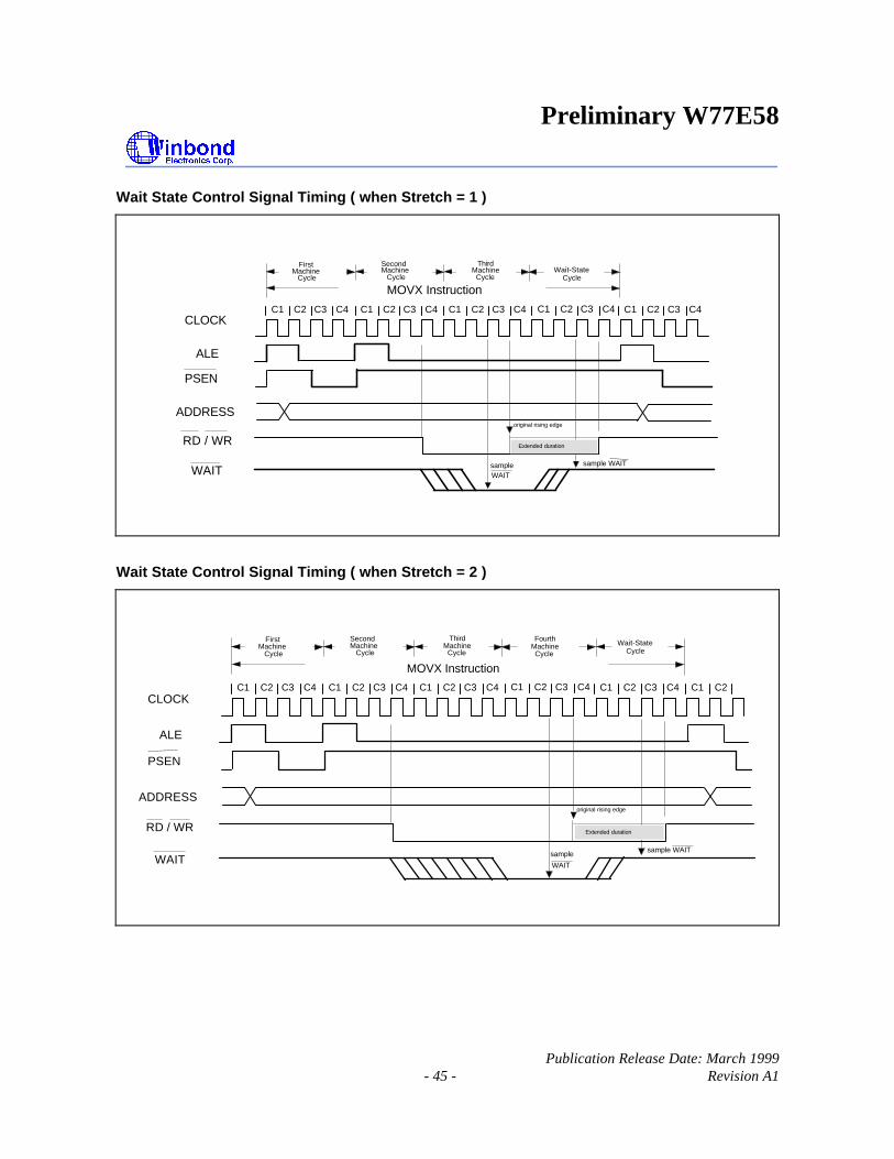
Preliminary W77E58
Publication Release Date: March 1999- 45 - Revision A1
Wait State Control Signal Timing ( when Stretch = 1 )
C2 C3 C4C1CLOCK
ALE
PSEN
ADDRESS
RD / WR
C2 C3 C4C1 C2 C3 C4C1 C2 C3 C4C1 C2 C3 C4C1
MOVX Instruction
FirstMachine
Cycle
SecondMachine
CycleWait-State
Cycle
ThirdMachine
Cycle
WAIT sampleWAIT
sample WAIT
Extended duration
original rising edge
Wait State Control Signal Timing ( when Stretch = 2 )
C2 C3 C4C1CLOCK
ALE
PSEN
ADDRESS
RD / WR
C2 C3 C4C1 C2 C3 C4C1 C2 C3 C4C1 C3 C4C2C1
MOVX Instruction
FirstMachine
Cycle
SecondMachine
CycleWait-State
Cycle
ThirdMachine
Cycle
WAITsample
WAIT
sample WAIT
Extended duration
original rising edge
C2C1
Cycle
FourthMachine

Preliminary W77E58
- 46 -
POWER MANAGEMENTThe W77E58 has several features that help the user to control the power consumption of the device.The power saving features are basically the POWER DOWN mode, ECONOMY mode and the IDLEmode of operation.
Idle Mode
The user can put the device into idle mode by writing 1 to the bit PCON.0. The instruction that setsthe idle bit is the last instruction that will be executed before the device goes into Idle Mode. In theIdle mode, the clock to the CPU is halted, but not to the Interrupt, Timer, Watchdog timer and Serialport blocks. This forces the CPU state to be frozen; the Program counter, the Stack Pointer, theProgram Status Word, the Accumulator and the other registers hold their contents. The ALE andPSEN pins are held high during the Idle state. The port pins hold the logical states they had at thetime Idle was activated. The Idle mode can be terminated in two ways. Since the interrupt controller isstill active, the activation of any enabled interrupt can wake up the processor. This will automaticallyclear the Idle bit, terminate the Idle mode, and the Interrupt Service Routine(ISR) will be executed.After the ISR, execution of the program will continue from the instruction which put the device intoIdle mode.
The Idle mode can also be exited by activating the reset. The device can be put into reset either byapplying a high on the external RST pin, a Power on reset condition or a Watchdog timer reset. Theexternal reset pin has to be held high for at least two machine cycles i.e. 8 clock periods to berecognized as a valid reset. In the reset condition the program counter is reset to 0000h and all theSFRs are set to the reset condition. Since the clock is already running there is no delay and executionstarts immediately. In the Idle mode, the Watchdog timer continues to run, and if enabled, a time-outwill cause a watchdog timer interrupt which will wake up the device. The software must reset theWatchdog timer in order to preempt the reset which will occur after 512 clock periods of the time-out.When the W77E58 is exiting from an Idle mode with a reset, the instruction following the one whichput the device into Idle mode is not executed. So there is no danger of unexpected writes.
Economy Mode
The power consumption of microcontroller relates to operating frequency. The W77E58 offers aEconomy mode to reduce the internal clock rate dynamically without external components. Bydefault, one machine cycle needs 4 clocks. In Economy mode, software can select 4, 64 or 1024clocks per machine cycle. It keeps the CPU operating at a acceptable speed but eliminates the powerconsumption. In the Idle mode, the clock of the core logic is stopped, but all clocked peripherals suchas watchdog timer are still running at a rate of clock/4. In the Economy mode, all clocked peripheralsrun at the same reduced clocks rate as in core logic. So the Economy mode may provide a lowerpower consumption than idle mode.
Software invokes the Economy mode by setting the appropriate bits in the SFRs. Setting the bitsCD0(PMR.6), CD1(PMR.7) decides the instruction cycle rate as below:
CD1 CD0 clocks/machine cycle 0 0 Reserved 0 1 4 (default) 1 0 64 1 1 1024

Preliminary W77E58
Publication Release Date: March 1999- 47 - Revision A1
The selection of instruction rate is going to take effect after a delay of one instruction cycle. Switchingto divide by 64 or 1024 mode must first go from divide by 4 mode. This means software can notswitch directly between clock/64 and clock/1024 mode. The CPU has to return clock/4 mode first,then go to clock/64 or clock/1024 mode.
The W77E58 allows the user to use internal RC oscillator instead of external crystal. Setting theXT/RG bit (EXIF.3) selects the crystal or RC oscillator as the clock source. When invoking RCoscillator in Economy mode, software may set the XTOFF bit to turn off the crystal amplifier forsaving power. The CPU would run at the clock rate of approximately 2−4 MHz divided by 4, 64 or1024. The RC oscillator is not precise so that can not be invoked to the operation which needs theaccurate time-base such as serial communication. The RGMD(EXIF.2) indicates current clock source.When switching the clock source, CPU needs one instruction cycle delay to take effect new setting. Ifcrystal amplifier is disabled and RC oscillator is present clock source, software must first clear theXTOFF bit to turn on crystal amplifier before switch to crystal operation. Hardware will set the XTUPbit (STATUS.4) once the crystal is warm-up and ready for use. It is unable to set XT/RG bit to 1 ifXTUP = 0.
In Economy mode, the serial port can not receive/transmit data correctly because the baud rate ischanged. In some systems, the external interrupts may require the fastest process such that thereducing of operating speed is restricted. In order to solve these dilemmas, the W77E58 offers aswitchback feature which allows the CPU back to clock/4 mode immediately when triggered by serialoperation or external interrupts. The switchback feature is enabled by setting the SWB bit (PMR.5). Aserial port reception/transmission or qualified external interrupt which is enabled and acknowledgedwithout block conditions will cause CPU to return to divide by 4 mode. For the serial port reception, aswitchback is generated by a falling edge associated with start bit if the serial port reception isenabled. When a serial port transmission, an instruction which writes a byte of data to serial portbuffer will cause a switchback to ensure the correct transmission. The switchback feature isunaffected by serial port interrupt flags. After a switchback is generated, the software can manuallyreturn the CPU to Economy mode. Note that the modification of clock control bits CD0 and CD1 willbe ignored during serial port transmit/receive when switchback is enabled. The Watchdog timer reset,power-on/fail reset or external reset will force the CPU to return to divide by 4 mode.
Power Down Mode
The device can be put into Power Down mode by writing 1 to bit PCON.1. The instruction that doesthis will be the last instruction to be executed before the device goes into Power Down mode. In thePower Down mode, all the clocks are stopped and the device comes to a halt. All activity iscompletely stopped and the power consumption is reduced to the lowest possible value. In this statethe ALE and PSEN pins are pulled low. The port pins output the values held by their respectiveSFRs.
The W77E58 will exit the Power Down mode with a reset or by an external interrupt pin enabled aslevel detect. An external reset can be used to exit the Power down state. The high on RST pinterminates the Power Down mode, and restarts the clock. The program execution will restart from0000h. In the Power down mode, the clock is stopped, so the Watchdog timer cannot be used toprovide the reset to exit Power down mode.

Preliminary W77E58
- 48 -
The W77E58 can be woken from the Power Down mode by forcing an external interrupt pin activated,provided the corresponding interrupt is enabled, while the global enable(EA) bit is set and the externalinput has been set to a level detect mode. If these conditions are met, then the low level on theexternal pin re-starts the oscillator. Then device executes the interrupt service routine for thecorresponding external interrupt. After the interrupt service routine is completed, the programexecution returns to the instruction after the one which put the device into Power Down mode andcontinues from there. When RGSL(EXIF.1) bit is set to 1, the CPU will use the internal RC oscillatorinstead of crystal to exit Power Down mode. The microcontroller will automatically switch from RCoscillator to crystal after clock is stable. The RC oscillator runs at approximately 2−4 MHz. Using RCoscillator to exit from Power Down mode saves the time for waiting crystal start-up. It is useful in thelow power system which usually be awakened from a short operation then returns to Power Downmode.
Table 5. Status of external pins during Idle and Power Down
Mode Program
Memory
ALE PSEN PORT0 PORT1 PORT2 PORT3
Idle Internal 1 1 Data Data Data Data
Idle External 1 1 Float Data Address Data
Power Down Internal 0 0 Data Data Data Data
Power Down External 0 0 Float Data Data Data
RESET CONDITIONSThe user has several hardware related options for placing the W77E58 into reset condition. Ingeneral, most register bits go to their reset value irrespective of the reset condition, but there are afew flags whose state depends on the source of reset. The user can use these flags to determine thecause of reset using software. There are two ways of putting the device into reset state. They areExternal reset and Watchdog reset.
External Reset
The device continuously samples the RST pin at state C4 of every machine cycle. Therefore the RSTpin must be held for at least 2 machine cycles to ensure detection of a valid RST high. The resetcircuitry then synchronously applies the internal reset signal. Thus the reset is a synchronousoperation and requires the clock to be running to cause an external reset.
Once the device is in reset condition, it will remain so as long as RST is 1. Even after RST isdeactivated, the device will continue to be in reset state for up to two machine cycles, and then beginprogram execution from 0000h. There is no flag associated with the external reset condition. Howeversince the other two reset sources have flags, the external reset can be considered as the default resetif those two flags are cleared.

Preliminary W77E58
Publication Release Date: March 1999- 49 - Revision A1
The software must clear the POR flag after reading it, otherwise it will not be possible to correctlydetermine future reset sources. If the power fails, i.e. falls below Vrst, then the device will once againgo into reset state. When the power returns to the proper operating levels, the device will againperform a power on reset delay and set the POR flag.
Watchdog Timer Reset
The Watchdog timer is a free running timer with programmable time-out intervals. The user can clearthe watchdog timer at any time, causing it to restart the count. When the time-out interval is reachedan interrupt flag is set. If the Watchdog reset is enabled and the watchdog timer is not cleared, then512 clocks from the flag being set, the watchdog timer will generate a reset . This places the deviceinto the reset condition. The reset condition is maintained by hardware for two machine cycles. Oncethe reset is removed the device will begin execution from 0000h.
RESET STATEMost of the SFRs and registers on the device will go to the same condition in the reset state. TheProgram Counter is forced to 0000h and is held there as long as the reset condition is applied.However, the reset state does not affect the on-chip RAM. The data in the RAM will be preservedduring the reset. However, the stack pointer is reset to 07h, and therefore the stack contents will belost. The RAM contents will be lost if the VDD falls below approximately 2V, as this is the minimumvoltage level required for the RAM to operate normally. Therefore after a first time power on reset theRAM contents will be indeterminate. During a power fail condition, if the power falls below 2V, theRAM contents are lost.
After a reset most SFRs are cleared. Interrupts and Timers are disabled. The Watchdog timer isdisabled if the reset source was a POR. The port SFRs have FFh written into them which puts theport pins in a high state. Port 0 floats as it does not have on-chip pull-ups.
Table 6. SFR Reset Value
SFR Name Reset Value SFR Name Reset ValueP0 11111111b IE 00000000b
SP 00000111b SADDR 00000000b
DPL 00000000b P3 11111111b
DPH 00000000b IP x0000000b
DPL1 00000000b SADEN 00000000b
DPH1 00000000b T2CON 00000000b
DPS 00000000b T2MOD 00000x00b
PCON 00xx0000b RCAP2L 00000000b
TCON 00000000b RCAP2H 00000000b
TMOD 00000000b TL2 00000000b
TL0 00000000b TH2 00000000b
TL1 00000000b TA 11111111b
TH0 00000000b PSW 00000000b
TH1 00000000b WDCON 0x0x0xx0b
CKCON 00000001b ACC 00000000b
P1 11111111b EIE xxx00000b

Preliminary W77E58
- 50 -
Table 6. SFR Reset Value, continued
SFR Name Reset Value SFR Name Reset ValueSCON 00000000b B 00000000b
SBUF xxxxxxxxb EIP xxx00000b
P2 11111111b PC 00000000b
SADDR1 00000000b SADEN1 00000000b
SCON1 00000000b SBUF1 xxxxxxxxb
ROMMAP 01xxx110b PMR 010xx0x0b
EXIF 0000xxx0b STATUS 000x0000b
P4 xxxx1111b
The WDCON SFR bits are set/cleared in reset condition depending on the source of the reset.
External reset Watchdog reset Power on reset
WDCON 0x0x0xx0b 0x0x01x0b 01000000b
The POR bit WDCON.6 is set only by the power on reset. The PFI bit WDCON.4 is set when thepower fail condition occurs. However, a power-on reset will clear this bit. The WTRF bit WDCON.2 isset when the Watchdog timer causes a reset. A power on reset will also clear this bit. The EWT bitWDCON.1 is cleared by power on resets. This disables the Watchdog timer resets. A watchdog orexternal reset does not affect the EWT bit.
INTERRUPTS
The W77E58 has a two priority level interrupt structure with 12 interrupt sources. Each of the interruptsources has an individual priority bit, flag, interrupt vector and enable bit. In addition, the interruptscan be globally enabled or disabled.
Interrupt Sources
The External Interrupts INT0 and INT1 can be either edge triggered or level triggered, depending onbits IT0 and IT1. The bits IE0 and IE1 in the TCON register are the flags which are checked togenerate the interrupt. In the edge triggered mode, the INTx inputs are sampled in every machinecycle. If the sample is high in one cycle and low in the next, then a high to low transition is detectedand the interrupts request flag IEx in TCON or EXIF is set. The flag bit requests the interrupt. Sincethe external interrupts are sampled every machine cycle, they have to be held high or low for at leastone complete machine cycle. The IEx flag is automatically cleared when the service routine is called.If the level triggered mode is selected, then the requesting source has to hold the pin low till theinterrupt is serviced. The IEx flag will not be cleared by the hardware on entering the service routine.If the interrupt continues to be held low even after the service routine is completed, then theprocessor may acknowledge another interrupt request from the same source. Note that the externalinterrupts INT2 to INT5 are edge triggered only. By default, the individual interrupt flag correspondingto external interrupt 2 to 5 must be cleared manually by software. It can be configured with hardwarecleared by setting the corresponding bit HCx in the T2MOD register. For instance, if HC2 is sethardware will clear IE2 flag after program enters the interrupt 2 service routine.

Preliminary W77E58
Publication Release Date: March 1999- 51 - Revision A1
The Timer 0 and 1 Interrupts are generated by the TF0 and TF1 flags. These flags are set by theoverflow in the Timer 0 and Timer 1. The TF0 and TF1 flags are automatically cleared by thehardware when the timer interrupt is serviced. The Timer 2 interrupt is generated by a logical OR ofthe TF2 and the EXF2 flags. These flags are set by overflow or capture/reload events in the timer 2operation. The hardware does not clear these flags when a timer 2 interrupt is executed. Software hasto resolve the cause of the interrupt between TF2 and EXF2 and clear the appropriate flag.
The Watchdog timer can be used as a system monitor or a simple timer. In either case, when thetime-out count is reached, the Watchdog timer interrupt flag WDIF (WDCON.3) is set. If the interruptis enabled by the enable bit EIE.4, then an interrupt will occur.
The Serial block can generate interrupts on reception or transmission. There are two interrupt sourcesfrom the Serial block, which are obtained by the RI and TI bits in the SCON SFR and RI_1 and TI_1in the SCON1 SFR. These bits are not automatically cleared by the hardware, and the user will haveto clear these bits using software.
All the bits that generate interrupts can be set or reset by hardware, and thereby software initiatedinterrupts can be generated. Each of the individual interrupts can be enabled or disabled by setting orclearing a bit in the IE SFR. IE also has a global enable/disable bit EA, which can be cleared todisable all the interrupts, except PFI, at once.
Priority Level Structure
There are three priority levels for the interrupts, highest, high and low. The interrupt sources can beindividually set to either high or low levels. Naturally, a higher priority interrupt cannot be interruptedby a lower priority interrupt. However there exists a pre-defined hierarchy amongst the interruptsthemselves. This hierarchy comes into play when the interrupt controller has to resolve simultaneousrequests having the same priority level. This hierarchy is defined as shown below; the interrupts arenumbered starting from the highest priority to the lowest.
Table 7. Priority structure of interrupts
Source Flag Priority levelExternal Interrupt 0 IE0 1(highest)Timer 0 Overflow TF0 2External Interrupt 1 IE1 3Timer 1 Overflow TF1 4Serial Port RI + TI 5Timer 2 Overflow TF2 + EXF2 6Serial Port 1 RI_1 + TI_1 7External Interrupt 2 IE2 8External Interrupt 3 IE3 9External Interrupt 4 IE4 10External Interrupt 5 IE5 11Watchdog Timer WDIF 12 (lowest)

Preliminary W77E58
- 52 -
The interrupt flags are sampled every machine cycle. In the same machine cycle, the sampledinterrupts are polled and their priority is resolved. If certain conditions are met then the hardware willexecute an internally generated LCALL instruction which will vector the process to the appropriateinterrupt vector address. The conditions for generating the LCALL are
1. An interrupt of equal or higher priority is not currently being serviced.
2. The current polling cycle is the last machine cycle of the instruction currently being executed.
3. The current instruction does not involve a write to IP, IE, EIP or EIE registers and is not a RETI.
If any of these conditions are not met, then the LCALL will not be generated. The polling cycle isrepeated every machine cycle, with the interrupts sampled in the same machine cycle. If an interruptflag is active in one cycle but not responded to, and is not active when the above conditions are met,the denied interrupt will not be serviced. This means that active interrupts are not remembered; everypolling cycle is new.
The processor responds to a valid interrupt by executing an LCALL instruction to the appropriateservice routine. This may or may not clear the flag which caused the interrupt. In case of Timerinterrupts, the TF0 or TF1 flags are cleared by hardware whenever the processor vectors to theappropriate timer service routine. In case of external interrupt, INT0 and INT1, the flags are clearedonly if they are edge triggered. In case of Serial interrupts, the flags are not cleared by hardware. Inthe case of Timer 2 interrupt, the flags are not cleared by hardware. The Watchdog timer interruptflag WDIF has to be cleared by software. The hardware LCALL behaves exactly like the softwareLCALL instruction. This instruction saves the Program Counter contents onto the Stack, but does notsave the Program Status Word PSW. The PC is reloaded with the vector address of that interruptwhich caused the LCALL. These vector address for the different sources are as follows
Table 8. Vector locations for interrupt sources
Source Vector Address Source Vector Address
Timer 0 Overflow 000Bh External Interrupt 0 0003h
Timer 1 Overflow 001Bh External Interrupt 1 0013h
Timer 2 Interrupt 002Bh Serial Port 0023h
External Interrupt 2 0043h Serial Port 1 003Bh
External Interrupt 4 0053h External Interrupt 3 004Bh
Watchdog Timer 0063h External Interrupt 5 005Bh
The vector table is not evenly spaced; this is to accommodate future expansions to the device family.

Preliminary W77E58
Publication Release Date: March 1999- 53 - Revision A1
Execution continues from the vectored address till an RETI instruction is executed. On execution ofthe RETI instruction the processor pops the Stack and loads the PC with the contents at the top of thestack. The user must take care that the status of the stack is restored to what is was after thehardware LCALL, if the execution is to return to the interrupted program. The processor does notnotice anything if the stack contents are modified and will proceed with execution from the addressput back into PC. Note that a RET instruction would perform exactly the same process as a RETIinstruction, but it would not inform the Interrupt Controller that the interrupt service routine iscompleted, and would leave the controller still thinking that the service routine is underway.
Interrupt Response Time
The response time for each interrupt source depends on several factors, such as the nature of theinterrupt and the instruction underway. In the case of external interrupts INT0 to INT5 , they aresampled at C3 of every machine cycle and then their corresponding interrupt flags IEx will be set orreset. The Timer 0 and 1 overflow flags are set at C3 of the machine cycle in which overflow hasoccurred. These flag values are polled only in the next machine cycle. If a request is active and allthree conditions are met, then the hardware generated LCALL is executed. This LCALL itself takesfour machine cycles to be completed. Thus there is a minimum time of five machine cycles betweenthe interrupt flag being set and the interrupt service routine being executed.
A longer response time should be anticipated if any of the three conditions are not met. If a higher orequal priority is being serviced, then the interrupt latency time obviously depends on the nature of theservice routine currently being executed. If the polling cycle is not the last machine cycle of theinstruction being executed, then an additional delay is introduced. The maximum response time (if noother interrupt is in service) occurs if the W77E58 is performing a write to IE, IP, EIE or EIP and thenexecutes a MUL or DIV instruction. From the time an interrupt source is activated, the longestreaction time is 12 machine cycles. This includes 1 machine cycle to detect the interrupt, 2 machinecycles to complete the IE, IP, EIE or EIP access, 5 machine cycles to complete the MUL or DIVinstruction and 4 machine cycles to complete the hardware LCALL to the interrupt vector location.
Thus in a single-interrupt system the interrupt response time will always be more than 5 machinecycles and not more than 12 machine cycles. The maximum latency of 12 machine cycle is 48 clockcycles. Note that in the standard 8051 the maximum latency is 8 machine cycles which equals 96machine cycles. This is a 50% reduction in terms of clock periods.
PROGRAMMABLE TIMERS/COUNTERS
The W77E58 has three 16-bit programmable timer/counters and one programmable Watchdog timer.The Watchdog timer is operationally quite different from the other two timers.
TIMER/COUNTERS 0 & 1
The W77E58 has two 16-bit Timer/Counters. Each of these Timer/Counters has two 8 bit registerswhich form the 16 bit counting register. For Timer/Counter 0 they are TH0, the upper 8 bits register,and TL0, the lower 8 bit register. Similarly Timer/Counter 1 has two 8 bit registers, TH1 and TL1. Thetwo can be configured to operate either as timers, counting machine cycles or as counters countingexternal inputs.

Preliminary W77E58
- 54 -
When configured as a "Timer", the timer counts clock cycles. The timer clock can be programmed tobe thought of as 1/12 of the system clock or 1/4 of the system clock. In the "Counter" mode, theregister is incremented on the falling edge of the external input pin, T0 in case of Timer 0, and T1 forTimer 1. The T0 and T1 inputs are sampled in every machine cycle at C4. If the sampled value ishigh in one machine cycle and low in the next, then a valid high to low transition on the pin isrecognized and the count register is incremented. Since it takes two machine cycles to recognize anegative transition on the pin, the maximum rate at which counting will take place is 1/24 of themaster clock frequency. In either the "Timer" or "Counter" mode, the count register will be updated atC3. Therefore, in the "Timer" mode, the recognized negative transition on pin T0 and T1 can causethe count register value to be updated only in the machine cycle following the one in which thenegative edge was detected.
The "Timer" or "Counter" function is selected by the " C T/ " bit in the TMOD Special FunctionRegister. Each Timer/Counter has one selection bit for its own; bit 2 of TMOD selects the function forTimer/Counter 0 and bit 6 of TMOD selects the function for Timer/Counter 1. In addition eachTimer/Counter can be set to operate in any one of four possible modes. The mode selection is doneby bits M0 and M1 in the TMOD SFR.
Time-Base Selection
The W77E58 gives the user two modes of operation for the timer. The timers can be programmed tooperate like the standard 8051 family, counting at the rate of 1/12 of the clock speed. This will ensurethat timing loops on the W77E58 and the standard 8051 can be matched. This is the default mode ofoperation of the W77E58 timers. The user also has the option to count in the turbo mode, where thetimers will increment at the rate of 1/4 clock speed. This will straight-away increase the countingspeed three times. This selection is done by the T0M and T1M bits in CKCON SFR. A reset setsthese bits to 0, and the timers then operate in the standard 8051 mode. The user should set these bitsto 1 if the timers are to operate in turbo mode.
MODE 0
In Mode 0, the timer/counters act as a 8 bit counter with a 5 bit, divide by 32 pre-scale. In this modewe have a 13 bit timer/counter. The 13 bit counter consists of 8 bits of THx and 5 lower bits of TLx.The upper 3 bits of TLx are ignored.The negative edge of the clock increments the count in the TLx register. When the fifth bit in TLxmoves from 1 to 0, then the count in the THx register is incremented. When the count in THx movesfrom FFh to 00h, then the overflow flag TFx in TCON SFR is set. The counted input is enabled only ifTRx is set and either GATE = 0 or INTx = 1. When C T/ is set to 0, then it will count clock cycles,
and if C T/ is set to 1, then it will count 1 to 0 transitions on T0 (P3.4) for timer 0 and T1 (P3.5) fortimer 1. When the 13 bit count reaches 1FFFh the next count will cause it to roll-over to 0000h. Thetimer overflow flag TFx of the relevant timer is set and if enabled an interrupts will occur. Note thatwhen used as a timer, the time-base may be either clock cycles/12 or clock cycles/4 as selected bythe bits TxM of the CKCON SFR.

Preliminary W77E58
Publication Release Date: March 1999- 55 - Revision A1
1/4
1/12
C/T = TMOD.2(C/T = TMOD.6)
T0M = CKCON.3(T1M = CKCON.4)
M1,M0 = TMOD.1,TMOD.0(M1,M0 = TMOD.5,TMOD.4)
Interrupt
T0 = P3.4(T1 = P3.5) TH0
(TH1)TL0
(TL1)
TF0(TF1)
TR0 = TCON.4(TR1 = TCON.6)
GATE = TMOD.3(GATE = TMOD.7)
INT0 = P3.2(INT1 = P3.3)
70
TFx
4 70
Timer 1 functions are shown in brackets
1
0000
101
Clock Source Mode inputdiv. by 4 osc/1div. by 64 osc/16div. by 1024 osc/256
Figure 11. Timer/Counter Mode 0 & Mode 1
MODE 1
Mode 1 is similar to Mode 0 except that the counting register forms a 16 bit counter, rather than a 13bit counter. This means that all the bits of THx and TLx are used. Roll-over occurs when the timermoves from a count of FFFFh to 0000h. The timer overflow flag TFx of the relevant timer is set and ifenabled an interrupt will occur. The selection of the time-base in the timer mode is similar to that inMode 0. The gate function operates similarly to that in Mode 0.
MODE 2
In Mode 2, the timer/counter is in the Auto Reload Mode. In this mode, TLx acts as a 8 bit countregister, while THx holds the reload value. When the TLx register overflows from FFh to 00h, the TFxbit in TCON is set and TLx is reloaded with the contents of THx, and the counting process continuesfrom here. The reload operation leaves the contents of the THx register unchanged. Counting isenabled by the TRx bit and proper setting of GATE and INTx pins. As in the other two modes 0 and 1mode 2 allows counting of either clock cycles (clock/12 or clock/4) or pulses on pin Tn.

Preliminary W77E58
- 56 -
1/4
1/12
T0M = CKCON.3(T1M = CKCON.4)
C/T = TMOD.2(C/T = TMOD.6)
InterruptT0 = P3.4
(T1 = P3.5)
TH0(TH1)
TL0(TL1)
TF0(TF1)
TR0 = TCON.4(TR1 = TCON.6)
GATE = TMOD.3(GATE = TMOD.7)
INT0 = P3.2(INT1 = P3.3)
70 TFx
70
Timer 1 functions are shown in brackets
1
00
1
Clock Source Mode inputdiv. by 4 osc/1div. by 64 osc/16div. by 1024 osc/256
Figure 12. Timer/Counter Mode 2.
MODE 3
Mode 3 has different operating methods for the two timer/counters. For timer/counter 1, mode 3simply freezes the counter. Timer/Counter 0, however, configures TL0 and TH0 as two separate 8 bitcount registers in this mode. The logic for this mode is shown in the figure. TL0 uses theTimer/Counter 0 control bits C T/ , GATE, TR0, INT0 and TF0. The TL0 can be used to count clockcycles (clock/12 or clock/4) or 1-to-0 transitions on pin T0 as determined by C/T (TMOD.2). TH0 isforced as a clock cycle counter (clock/12 or clock/4) and takes over the use of TR1 and TF1 fromTimer/Counter 1. Mode 3 is used in cases where an extra 8 bit timer is needed. With Timer 0 in Mode3, Timer 1 can still be used in Modes 0, 1 and 2., but its flexibility is somewhat limited. While its basicfunctionality is maintained, it no longer has control over its overflow flag TF1 and the enable bit TR1.Timer 1 can still be used as a timer/counter and retains the use of GATE and INT1 pin. In thiscondition it can be turned on and off by switching it out of and into its own Mode 3. It can also be usedas a baud rate generator for the serial port.
TIMER/COUNTER 2
Timer/Counter 2 is a 16 bit up/down counter which is configured by the T2MOD register andcontrolled by the T2CON register. Timer/Counter 2 is equipped with a capture/reload capability. Aswith the Timer 0 and Timer 1 counters, there exists considerable flexibility in selecting and controllingthe clock, and in defining the operating mode. The clock source for Timer/Counter 2 may be selectedfor either the external T2 pin (C/T2 = 1) or the crystal oscillator, which is divided by 12 or 4 (C/T2 =0). The clock is then enabled when TR2 is a 1, and disabled when TR2 is a 0.

Preliminary W77E58
Publication Release Date: March 1999- 57 - Revision A1
1/4
1/12
T0M = CKCON.3
Interrupt
C/T = TMOD.2
T0 = P3.4
TH0
TL0
TR0 = TCON.4
GATE = TMOD.3
TR1 = TCON.6
INT0 = P3.2
70
TF170
InterruptTF0
10
0
1
Clock Source Mode inputdiv. by 4 osc/1div. by 64 osc/16div. by 1024 osc/256
Figure 13. Timer/Counter 0 Mode 3
CAPTURE MODE
The capture mode is enabled by setting the CP RL/ 2 bit in the T2CON register to a 1. In the capturemode, Timer/Counter 2 serves as a 16 bit up counter. When the counter rolls over from FFFFh to0000h, the TF2 bit is set, which will generate an interrupt request. If the EXEN2 bit is set, then anegative transition of T2EX pin will cause the value in the TL2 and TH2 register to be captured by theRCAP2L and RCAP2H registers. This action also causes the EXF2 bit in T2CON to be set, which willalso generate an interrupt. Setting the T2CR bit (T2MOD.3), the W77E58 allows hardware to resettimer 2 automatically after the value of TL2 and TH2 have been captured.
1/4Clock Source
Mode inputdiv. by 4 osc/1div. by 64 osc/16div. by 1024 osc/256 1/12
T2M = CKCON.5
C/T2 = T2CON.1
T2CON.7
T2 = P1.0
T2CON.6
TR2 = T2CON.2
T2EX = P1.1
EXEN2 = T2CON.3 EXF2
Timer 2Interrupt
TF2TH2TL2
RCAP2HRCAP2L
1
00
1
Figure 14. 16-Bit Capture Mode

Preliminary W77E58
- 58 -
AUTO-RELOAD MODE, COUNTING UP
The auto-reload mode as an up counter is enabled by clearing the CP RL/ 2 bit in the T2CON registerand clearing the DCEN bit in T2MOD register. In this mode, Timer/Counter 2 is a 16 bit up counter.When the counter rolls over from FFFFh, a reload is generated that causes the contents of theRCAP2L and RCAP2H registers to be reloaded into the TL2 and TH2 registers. The reload action alsosets the TF2 bit. If the EXEN2 bit is set, then a negative transition of T2EX pin will also cause areload. This action also sets the EXF2 bit in T2CON.
1/4
1/12
T2M = CKCON.5
C/T2 = T2CON.1T2CON.7
T2 = P1.0
T2CON.6
TR2 = T2CON.2
T2EX = P1.1
EXEN2 = T2CON.3 EXF2
Timer 2Interrupt
TF2TH2TL2
RCAP2HRCAP2L
1
00
1
Clock Source Mode inputdiv. by 4 osc/1div. by 64 osc/16div. by 1024 osc/256
Figure 15. 16-Bit Auto-reload Mode, Counting Up
AUTO-RELOAD MODE, COUNTING UP/DOWN
Timer/Counter 2 will be in auto-reload mode as an up/down counter if CP RL/ 2 bit in T2CON iscleared and the DCEN bit in T2MOD is set. In this mode, Timer/Counter 2 is an up/down counterwhose direction is controlled by the T2EX pin. A 1 on this pin cause the counter to count up. Anoverflow while counting up will cause the counter to be reloaded with the contents of the captureregisters. The next down count following the case where the contents of Timer/Counter equal thecapture registers will load an FFFFh into Timer/Counter 2. In either event a reload will set the TF2 bit.A reload will also toggle the EXF2 bit. However, the EXF2 bit can not generate an interrupt while inthis mode.

Preliminary W77E58
Publication Release Date: March 1999- 59 - Revision A1
C/T = T2CON.11/4
1/12
T2M = CKCON.5
Down Counting Reload Value
T2CON.7
Up Counting Reload Value
T2 = P1.0
T2CON.6
TR2 = T2CON.2
T2EX = P1.1 EXF2
Timer 2InterruptTF2TH2TL2
RCAP2HRCAP2L
10
01
0FFh0FFh
DCEN = 1
Clock Source Mode inputdiv. by 4 osc/1div. by 64 osc/16div. by 1024 osc/256
Figure 16. 16-Bit Auto-reload Up/Down Counter
BAUD RATE GENERATOR MODE
The baud rate generator mode is enabled by setting either the RCLK or TCLK bits in T2CON register.While in the baud rate generator mode, Timer/Counter 2 is a 16 bit counter with auto reload when thecount rolls over from FFFFh. However, rolling over does not set the TF2 bit. If EXEN2 bit is set, thena negative transition of the T2EX pin will set EXF2 bit in the T2CON register and cause an interruptrequest.
C/T = T2CON.1
T2 = P1.0
T2CON.6
TR2 = T2CON.2
T2EX = P1.1
EXEN2 = T2CON.3 EXF2
Timer 2overflow
Timer 2Interrupt
TH2TL2
RCAP2HRCAP2L
0
1
Clock Source Mode inputdiv. by 4 osc/2div. by 64 osc/32div. by 1024 osc/512
Figure 17. Baud Rate Generator Mode

Preliminary W77E58
- 60 -
PROGRAMMABLE CLOCK-OUT
Timer 2 is equipped with a new clock-out feature which outputs a 50% duty cycle clock on P1.0. It canbe invoked as a programmable clock generator. To configure Timer 2 with clock-out mode, softwaremust initiate it by setting bit T2OE = 1, C/T2 = 0 and CP/RL = 0. Setting bit TR2 will start the timer.This mode is similar to the baud rate generator mode, it will not generate an interrupt while Timer 2overflow. So it is possible to use Timer 2 as a baud rate generator and a clock generator at the sametime. The clock-out frequency is determined by the following equation:
The Clock-Out Frequency = Oscillator Frequency / [4 X (RCAP2H,RCAP2L) ]
T2CON.6
TR2 = T2CON.2
T2EX = P1.1
EXEN2 = T2CON.3 EXF2
T2=P1.0
Timer 2Interrupt
TH2TL2
RCAP2HRCAP2L
Clock Source Mode inputdiv. by 4 osc/2div. by 64 osc/32div. by 1024 osc/512
1/2
Figure 18. Programmable Clock-Out Mode
WATCHDOG TIMER
The Watchdog timer is a free-running timer which can be programmed by the user to serve as asystem monitor, a time-base generator or an event timer. It is basically a set of dividers that dividethe system clock. The divider output is selectable and determines the time-out interval. When thetime-out occurs a flag is set, which can cause an interrupt if enabled, and a system reset can also becaused if it is enabled. The interrupt will occur if the individual interrupt enable and the global enableare set. The interrupt and reset functions are independent of each other and may be used separatelyor together depending on the users software.
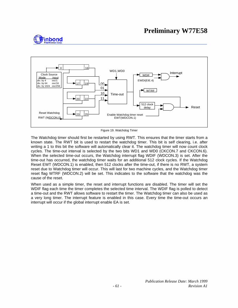
Preliminary W77E58
Publication Release Date: March 1999- 61 - Revision A1
16WD1,WD0
0001
10
11
Interrupt
Reset
Enable Watchdog timer resetEWT(WDCON.1)
Reset Watchdog
RWT (WDCON.0)
0
17 19
20 22
23 25
Time-out
WDIF
WTRF
512 clockdelay
EWDI(EIE.4)
Clock Source Mode inputdiv. by 4 osc/1div. by 64 osc/16div. by 1024 osc/256
Figure 19. Watchdog Timer
The Watchdog timer should first be restarted by using RWT. This ensures that the timer starts from aknown state. The RWT bit is used to restart the watchdog timer. This bit is self clearing, i.e. afterwriting a 1 to this bit the software will automatically clear it. The watchdog timer will now count clockcycles. The time-out interval is selected by the two bits WD1 and WD0 (CKCON.7 and CKCON.6).When the selected time-out occurs, the Watchdog interrupt flag WDIF (WDCON.3) is set. After thetime-out has occurred, the watchdog timer waits for an additional 512 clock cycles. If the WatchdogReset EWT (WDCON.1) is enabled, then 512 clocks after the time-out, if there is no RWT, a systemreset due to Watchdog timer will occur. This will last for two machine cycles, and the Watchdog timerreset flag WTRF (WDCON.2) will be set. This indicates to the software that the watchdog was thecause of the reset.
When used as a simple timer, the reset and interrupt functions are disabled. The timer will set theWDIF flag each time the timer completes the selected time interval. The WDIF flag is polled to detecta time-out and the RWT allows software to restart the timer. The Watchdog timer can also be used asa very long timer. The interrupt feature is enabled in this case. Every time the time-out occurs aninterrupt will occur if the global interrupt enable EA is set.

Preliminary W77E58
- 62 -
The main use of the Watchdog timer is as a system monitor. This is important in real-time controlapplications. In case of some power glitches or electro-magnetic interference, the processor maybegin to execute errant code. If this is left unchecked the entire system may crash. Using thewatchdog timer interrupt during software development will allow the user to select ideal watchdogreset locations. The code is first written without the watchdog interrupt or reset. Then the watchdoginterrupt is enabled to identify code locations where interrupt occurs. The user can now insertinstructions to reset the watchdog timer which will allow the code to run without any watchdog timerinterrupts. Now the watchdog timer reset is enabled and the watchdog interrupt may be disabled. Ifany errant code is executed now, then the reset watchdog timer instructions will not be executed atthe required instants and watchdog reset will occur.
The watchdog time-out selection will result in different time-out values depending on the clock speed.The reset, when enabled, will occur 512 clocks after the time-out has occurred.
Table 9. Time-out values for the Watchdog timer
WD1 WD0 WatchdogInterval
Number ofClocks
Time@ 1.8432 MHz
Time@ 10 MHz
Time@ 25 MHz
0 0 217 131072 71.11 mS 13.11 mS 5.24 mS
0 1 220 1048576 568.89 mS 104.86 mS 41.94 mS
1 0 223 8388608 4551.11 mS 838.86 mS 335.54 mS
1 1 226 67108864 36408.88 mS 6710.89 mS 2684.35 mS
The Watchdog timer will de disabled by a power-on/fail reset. The Watchdog timer reset does notdisable the watchdog timer, but will restart it. In general, software should restart the timer to put it intoa known state.
The control bits that support the Watchdog timer are discussed below.
WATCHDOG CONTROL
WDIF: WDCON.3 - Watchdog Timer Interrupt flag. This bit is set whenever the time-out occurs inthe watchdog timer. If the Watchdog interrupt is enabled (EIE.4), then an interrupt will occur(if the global interrupt enable is set and other interrupt requirements are met). Software or anyreset can clear this bit.
WTRF: WDCON.2 - Watchdog Timer Reset flag. This bit is set whenever a watchdog reset occurs.This bit is useful for determined the cause of a reset. Software must read it, and clear itmanually. A Power-fail reset will clear this bit. If EWT = 0, then this bit will not be affected bythe watchdog timer.
EWT: WDCON.1 - Enable Watchdog timer Reset. This bit when set to 1 will enable the Watchdogtimer reset function. Setting this bit to 0 will disable the Watchdog timer reset function, butwill leave the timer running.

Preliminary W77E58
Publication Release Date: March 1999- 63 - Revision A1
RWT: WDCON.0 - Reset Watchdog Timer. This bit is used to clear the Watchdog timer and torestart it. This bit is self-clearing, so after the software writes 1 to it the hardware willautomatically clear it. If the Watchdog timer reset is enabled, then the RWT has to be set bythe user within 512 clocks of the time-out. If this is not done then a Watchdog timer reset willoccur.
CLOCK CONTROL
WD1, WD0: CKCON.7, CKCON.6 - Watchdog Timer Mode select bits. These two bits select the time-out interval for the watchdog timer. The reset time is 512 clock longer than the interrupttime-out value.
The default Watchdog time-out is 217
clocks, which is the shortest time-out period. The EWT, WDIFand RWT bits are protected by the Timed Access procedure. This prevents software from accidentallyenabling or disabling the watchdog timer. More importantly, it makes it highly improbable that errantcode can enable or disable the watchdog timer.
SERIAL PORT
Serial port in the W77E58 is a full duplex port. The W77E58 provides the user with additional featuressuch as the Frame Error Detection and the Automatic Address Recognition. The serial ports arecapable of synchronous as well as asynchronous communication. In Synchronous mode the W77E58generates the clock and operates in a half duplex mode. In the asynchronous mode, full duplexoperation is available. This means that it can simultaneously transmit and receive data. The transmitregister and the receive buffer are both addressed as SBUF Special Function Register. However anywrite to SBUF will be to the transmit register, while a read from SBUF will be from the receive bufferregister. The serial port can operate in four different modes as described below.
MODE 0
This mode provides synchronous communication with external devices. In this mode serial data istransmitted and received on the RXD line. TXD is used to transmit the shift clock. The TxD clock isprovided by the W77E58 whether the device is transmitting or receiving. This mode is therefore a halfduplex mode of serial communication. In this mode, 8 bits are transmitted or received per frame. TheLSB is transmitted/received first. The baud rate is fixed at 1/12 or 1/4 of the oscillator frequency. Thisbaud rate is determined by the SM2 bit (SCON.5). When this bit is set to 0, then the serial port runs at1/12 of the clock. When set to 1, the serial port runs at 1/4 of the clock. This additional facility ofprogrammable baud rate in mode 0 is the only difference between the standard 8051 and theW77E58.
The functional block diagram is shown below. Data enters and leaves the Serial port on the RxD line.The TxD line is used to output the shift clock. The shift clock is used to shift data into and out of theW77E58 and the device at the other end of the line. Any instruction that causes a write to SBUF willstart the transmission. The shift clock will be activated and data will be shifted out on the RxD pin tillall 8 bits are transmitted. If SM2 = 1, then the data on RxD will appear 1 clock period before thefalling edge of shift clock on TxD. The clock on TxD then remains low for 2 clock periods, and thengoes high again. If SM2 = 0, the data on RxD will appear 3 clock periods before the falling edge ofshift clock on TxD. The clock on TxD then remains low for 6 clock periods, and then goes high again.This ensures that at the receiving end the data on RxD line can either be clocked on the rising edgeof the shift clock on TxD or latched when the TxD clock is low.
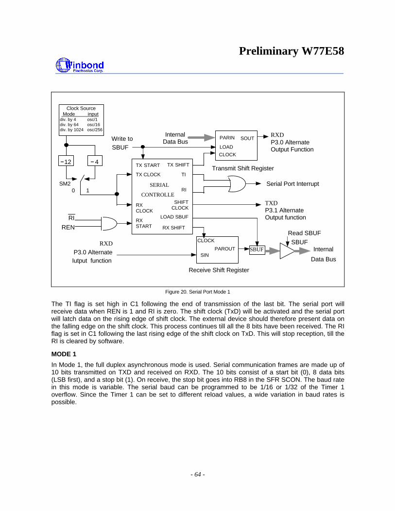
Preliminary W77E58
- 64 -
SBUF
Transmit Shift Register
Receive Shift Register
TX SHIFT
PAROUT
InternalData Bus
Internal
Data Bus
RXDP3.0 AlternateOutput Function
TXDP3.1 AlternateOutput function
RXD
P3.0 AlternateIutput function
Serial Port Interrupt
Write toSBUF
TX START
SOUT
TI
RI
REN
PARIN
LOAD
CLOCK
Read SBUF
SBUF
TX CLOCK
RISERIAL
CONTROLLESHIFT
CLOCKRXCLOCK
LOAD SBUFRXSTART RX SHIFT
CLOCK
SIN
412
10SM2
Clock Source Mode inputdiv. by 4 osc/1div. by 64 osc/16div. by 1024 osc/256
Figure 20. Serial Port Mode 1
The TI flag is set high in C1 following the end of transmission of the last bit. The serial port willreceive data when REN is 1 and RI is zero. The shift clock (TxD) will be activated and the serial portwill latch data on the rising edge of shift clock. The external device should therefore present data onthe falling edge on the shift clock. This process continues till all the 8 bits have been received. The RIflag is set in C1 following the last rising edge of the shift clock on TxD. This will stop reception, till theRI is cleared by software.
MODE 1
In Mode 1, the full duplex asynchronous mode is used. Serial communication frames are made up of10 bits transmitted on TXD and received on RXD. The 10 bits consist of a start bit (0), 8 data bits(LSB first), and a stop bit (1). On receive, the stop bit goes into RB8 in the SFR SCON. The baud ratein this mode is variable. The serial baud can be programmed to be 1/16 or 1/32 of the Timer 1overflow. Since the Timer 1 can be set to different reload values, a wide variation in baud rates ispossible.

Preliminary W77E58
Publication Release Date: March 1999- 65 - Revision A1
Transmission begins with a write to SBUF. The serial data is brought out on to TxD pin at C1following the first roll-over of divide by 16 counter. The next bit is placed on TxD pin at C1 followingthe next rollover of the divide by 16 counter. Thus the transmission is synchronized to the divide by16 counter and not directly to the write to SBUF signal. After all 8 bits of data are transmitted, the stopbit is transmitted. The TI flag is set in the C1 state after the stop bit has been put out on TxD pin. Thiswill be at the 10th rollover of the divide by 16 counter after a write to SBUF.
Reception is enabled only if REN is high. The serial port actually starts the receiving of serial data,with the detection of a falling edge on the RxD pin. The 1-to-0 detector continuously monitors the RxDline, sampling it at the rate of 16 times the selected baud rate. When a falling edge is detected, thedivide by 16 counter is immediately reset. This helps to align the bit boundaries with the rollovers ofthe divide by 16 counter.
The 16 states of the counter effectively divide the bit time into 16 slices. The bit detection is done ona best of three basis. The bit detector samples the RxD pin, at the 8th, 9th and 10th counter states.By using a majority 2 of 3 voting system, the bit value is selected. This is done to improve the noiserejection feature of the serial port. If the first bit detected after the falling edge of RxD pin is not 0,then this indicates an invalid start bit, and the reception is immediately aborted. The serial port againlooks for a falling edge in the RxD line. If a valid start bit is detected, then the rest of the bits are alsodetected and shifted into the SBUF.
After shifting in 8 data bits, there is one more shift to do, after which the SBUF and RB8 are loadedand RI is set. However certain conditions must be met before the loading and setting of RI can bedone.
1. RI must be 0 and
2. Either SM2 = 0, or the received stop bit = 1.
If these conditions are met, then the stop bit goes to RB8, the 8 data bits go into SBUF and RI is set.Otherwise the received frame may be lost. After the middle of the stop bit, the receiver goes back tolooking for a 1-to-0 transition on the RxD pin.

Preliminary W77E58
- 66 -
SBUF
RB8
Transmit Shift Register
Receive Shift Register
TX SHIFT
PAROUT
D8
InternalData Bus
InternalDataBus
TXD
RXD
Serial PortInterrupt
SMOD=(SMOD_1)
TCLK
RCLK
SAMPLE
Write toSBUF
TX START
SOUT
0 1
0 1
TI
10
PARIN
STOP
STARTLOAD
CLOCK
ReadSBUF
Timer 2 Overflow(for Serial Port 0 only)
Timer 1Overflow
TX CLOCK
RISERIAL
CONTROLLER
RX CLOCKLOAD
SBUFRX
START RX SHIFT
2
16
1-TO-0DETECTOR
BITDETECTOR
16
CLOCK
SIN
Figure 21. Serial Port Mode 1
MODE 2
This mode uses a total of 11 bits in asynchronous full-duplex communication. The functionaldescription is shown in the figure below. The frame consists of one start bit (0), 8 data bits (LSB first),a programmable 9th bit (TB8) and a stop bit (0). The 9th bit received is put into RB8. The baud rate isprogrammable to 1/32 or 1/64 of the oscillator frequency, which is determined by the SMOD bit inPCON SFR. Transmission begins with a write to SBUF. The serial data is brought out on to TxD pinat C1 following the first roll-over of the divide by 16 counter. The next bit is placed on TxD pin at C1following the next rollover of the divide by 16 counter. Thus the transmission is synchronized to thedivide by 16 counter, and not directly to the write to SBUF signal. After all 9 bits of data aretransmitted, the stop bit is transmitted. The TI flag is set in the C1 state after the stop bit has been putout on TxD pin. This will be at the 11th rollover of the divide by 16 counter after a write to SBUF.Reception is enabled only if REN is high. The serial port actually starts the receiving of serial data,with the detection of a falling edge on the RxD pin. The 1-to-0 detector continuously monitors the RxDline, sampling it at the rate of 16 times the selected baud rate. When a falling edge is detected, thedivide by 16 counter is immediately reset. This helps to align the bit boundaries with the rollovers ofthe divide by 16 counter. The 16 states of the counter effectively divide the bit time into 16 slices. Thebit detection is done on a best of three basis. The bit detector samples the RxD pin, at the 8th, 9thand 10th counter states. By using a majority 2 of 3 voting system, the bit value is selected. This isdone to improve the noise rejection feature of the serial port.

Preliminary W77E58
Publication Release Date: March 1999- 67 - Revision A1
SBUF
RB8
Transmit Shift Register
Receive Shift Register
TXSHIFT
PAROUT
D8
InternalData Bus
InternalDataBus
TXD
RXD
Serial PortInterrupt
SMOD=(SMOD_1)
SAMPLE
Write toSBUF
TX START
SOUT
0 1
TI
PARIN
STOP
START
LOAD
CLOCK
ReadSBUF
TX CLOCK
RI
SERIAL
CONTROLLER
RX CLOCKLOADSBUFRX START
RX SHIFT
2
16
1-TO-0DETECTOR
BITDETECTOR
16
CLOCK
SIN
D8TB8
Clock Source Mode inputdiv. by 4 osc/2div. by 64 osc/32div. by 1024 osc/512
Figure 22. Serial Port Mode 2
If the first bit detected after the falling edge of RxD pin, is not 0, then this indicates an invalid start bit,and the reception is immediately aborted. The serial port again looks for a falling edge in the RxDline. If a valid start bit is detected, then the rest of the bits are also detected and shifted into theSBUF. After shifting in 9 data bits, there is one more shift to do, after which the SBUF and RB8 areloaded and RI is set. However certain conditions must be met before the loading and setting of RI canbe done.1. RI must be 0 and2. Either SM2 = 0, or the received stop bit = 1.If these conditions are met, then the stop bit goes to RB8, the 8 data bits go into SBUF and RI is set.Otherwise the received frame may be lost. After the middle of the stop bit, the receiver goes back tolooking for a 1-to-0 transition on the RxD pin.

Preliminary W77E58
- 68 -
MODE 3
This mode is similar to Mode 2 in all respects, except that the baud rate is programmable. The usermust first initialize the Serial related SFR SCON before any communication can take place. Thisinvolves selection of the Mode and baud rate. The Timer 1 should also be initialized if modes 1 and 3are used. In all four modes, transmission is started by any instruction that uses SBUF as a destinationregister. Reception is initiated in Mode 0 by the condition RI = 0 and REN = 1. This will generate aclock on the TxD pin and shift in 8 bits on the RxD pin. Reception is initiated in the other modes bythe incoming start bit if REN = 1. The external device will start the communication by transmitting thestart bit.
SBUF
RB8
Transmit Shift Register
Receive Shift Register
TX SHIFT
PAROUT
D8
InternalData Bus
InternalDataBus
TXD
RXD
Serial PortInterrupt
SMOD=(SMOD_1)
TCLK
RCLK
SAMPLE
Write toSBUF
TX START
SOUT
0 1
0 1
TI
10
PARIN
STOP
STARTLOAD
CLOCK
ReadSBUF
Timer 2 Overflow(for Serial Port 0 only)
Timer 1Overflow
TX CLOCK
RISERIAL
CONTROLLER
RX CLOCKLOADSBUFRX
START RX SHIFT
2
16
1-TO-0DETECTOR
BITDETECTOR
16
CLOCK
SIN
D8TB8
Figure 23. Serial Port Mode 3
Table 10. Serial Ports Modes
SM1 SM0 Mode Type Baud Clock Framesize
Startbit
Stopbit
9th bitfunction
0 0 0 Synch. 4 or 12 TCLKS 8 bits No No None0 1 1 Asynch. Timer 1 or 2 10 bits 1 1 None1 0 2 Asynch. 32 or 64 TCLKS 11 bits 1 1 0, 11 1 3 Asynch. Timer 1 or 2 11 bits 1 1 0, 1

Preliminary W77E58
Publication Release Date: March 1999- 69 - Revision A1
Framing Error Detection
A Frame Error occurs when a valid stop bit is not detected. This could indicate incorrect serial datacommunication. Typically the frame error is due to noise and contention on the serial communicationline. The W77E58 has the facility to detect such framing errors and set a flag which can be checkedby software.
The Frame Error FE(FE_1) bit is located in SCON.7(SCON1.7). This bit is normally used as SM0 inthe standard 8051 family. However, in the W77E58 it serves a dual function and is called SM0/FE(SM0_1/FE_1). There are actually two separate flags, one for SM0 and the other for FE. The flag thatis actually accessed as SCON.7(SCON1.7) is determined by SMOD0 (PCON.6) bit. When SMOD0 isset to 1, then the FE flag is indicated in SM0/FE. When SMOD0 is set to 0, then the SM0 flag isindicated in SM0/FE.
The FE bit is set to 1 by hardware but must be cleared by software. Note that SMOD0 must be 1 whilereading or writing to FE or FE_1. If FE is set, then any following frames received without any error willnot clear the FE flag. The clearing has to be done by software.
Multiprocessor Communications
Multiprocessor communications makes use of the 9th data bit in modes 2 and 3. In the W77E58, theRI flag is set only if the received byte corresponds to the Given or Broadcast address. This hardwarefeature eliminates the software overhead required in checking every received address, and greatlysimplifies the software programmer task.
In the multiprocessor communication mode, the address bytes are distinguished from the data bytesby transmitting the address with the 9th bit set high. When the master processor wants to transmit ablock of data to one of the slaves, it first sends out the address of the targeted slave (or slaves). Allthe slave processors should have their SM2 bit set high when waiting for an address byte. Thisensures that they will be interrupted only by the reception of a address byte. The Automatic addressrecognition feature ensures that only the addressed slave will be interrupted. The address comparisonis done in hardware not software.
The addressed slave clears the SM2 bit, thereby clearing the way to receive data bytes. With SM2 =0, the slave will be interrupted on the reception of every single complete frame of data. Theunaddressed slaves will be unaffected, as they will be still waiting for their address. In Mode 1, the 9thbit is the stop bit, which is 1 in case of a valid frame. If SM2 is 1, then RI is set only if a valid frame isreceived and the received byte matches the Given or Broadcast address.
The Master processor can selectively communicate with groups of slaves by using the GivenAddress. All the slaves can be addressed together using the Broadcast Address. The addresses foreach slave are defined by the SADDR and SADEN SFRs. The slave address is an 8-bit valuespecified in the SADDR SFR. The SADEN SFR is actually a mask for the byte value in SADDR. If abit position in SADEN is 0, then the corresponding bit position in SADDR is don't care. Only those bitpositions in SADDR whose corresponding bits in SADEN are 1 are used to obtain the Given Address.This gives the user flexibility to address multiple slaves without changing the slave address inSADDR.

Preliminary W77E58
- 70 -
The following example shows how the user can define the Given Address to address different slaves.
Slave 1:SADDR1010 0100SADEN 1111 1010Given 1010 0x0x
Slave 2:SADDR1010 0111SADEN 1111 1001Given 1010 0xx1
The Given address for slave 1 and 2 differ in the LSB. For slave 1, it is a don't care, while for slave 2it is 1. Thus to communicate only with slave 1, the master must send an address with LSB = 0 (10100000). Similarly the bit 1 position is 0 for slave 1 and don't care for slave 2. Hence to communicateonly with slave 2 the master has to transmit an address with bit 1 = 1 (1010 0011). If the masterwishes to communicate with both slaves simultaneously, then the address must have bit 0 = 1 and bit1 = 0. The bit 3 position is don't care for both the slaves. This allows two different addresses to selectboth slaves (1010 0001 and 1010 0101).
The master can communicate with all the slaves simultaneously with the Broadcast Address. Thisaddress is formed from the logical ORing of the SADDR and SADEN SFRs. The zeros in the resultare defined as don't cares In most cases the Broadcast Address is FFh. In the previous case, theBroadcast Address is (1111111X) for slave 1 and (11111111) for slave 2.
The SADDR and SADEN SFRs are located at address A9h and B9h respectively. On reset, these twoSFRs are initialized to 00h. This results in Given Address and Broadcast Address being set as XXXXXXXX(i.e. all bits don't care). This effectively removes the multiprocessor communications feature,since any selectivity is disabled.
TIMED ACCESS PROTECTION
The W77E58 has several new features, like the Watchdog timer, on-chip ROM size adjustment, waitstate control signal and Power on/fail reset flag, which are crucial to proper operation of the system. Ifleft unprotected, errant code may write to the Watchdog control bits resulting in incorrect operationand loss of control. In order to prevent this, the W77E58 has a protection scheme which controls thewrite access to critical bits. This protection scheme is done using a timed access.
In this method, the bits which are to be protected have a timed write enable window. A write issuccessful only if this window is active, otherwise the write will be discarded. This write enablewindow is open for 3 machine cycles if certain conditions are met. After 3 machine cycles, thiswindow automatically closes. The window is opened by writing AAh and immediately 55h to the TimedAccess(TA) SFR. This SFR is located at address C7h. The suggested code for opening the timedaccess window is
TA REG 0C7h ;define new register TA, located at 0C7h
MOV TA, #0AAh
MOV TA, #055h

Preliminary W77E58
Publication Release Date: March 1999- 71 - Revision A1
When the software writes AAh to the TA SFR, a counter is started. This counter waits for 3 machinecycles looking for a write of 55h to TA. If the second write (55h) occurs within 3 machine cycles of thefirst write (AAh), then the timed access window is opened. It remains open for 3 machine cycles,during which the user may write to the protected bits. Once the window closes the procedure must berepeated to access the other protected bits.
Examples of Timed Assessing are shown below.
Example 1: Valid accessMOV TA, #0AAh 3 M/C Note: M/C = Machine CyclesMOV TA, #055h 3 M/CMOV WDCON, #00h 3 M/C
Example 2: Valid accessMOV TA, #0AAh 3 M/CMOV TA, #055h 3 M/CNOP 1 M/CSETB EWT 2 M/C
Example 3: Invalid accessMOV TA, #0AAh 3 M/CMOV TA, #055h 3 M/CNOP 1 M/CNOP 1 M/CCLR POR 2 M/C
Example 4: Invalid AccessMOV TA, #0AAh 3 M/CNOP 1 M/CMOV TA, #055h 3 M/CSETB EWT 2 M/C
In the first two examples, the writing to the protected bits is done before the 3 machine cycle windowcloses. In Example 3, however, the writing to the protected bit occurs after the window has closed,and so there is effectively no change in the status of the protected bit. In Example 4, the second writeto TA occurs 4 machine cycles after the first write, therefore the timed access window in not openedat all, and the write to the protected bit fails.
ON-CHIP MTP ROM CHARACTERISTICSThe W77E58 has several modes to program the on-chip MTP ROM. All these operations areconfigured by the pins RST, ALE, PSEN PSEN, A9CTRL(P3.0), A13CTRL(P3.1), A14CTRL(P3.2),
OECTRL(P3.3), CE (P3.6), OE (P3.7), A0(P1.0) and VPP(EA ). Moreover, the A15−A0(P2.7−P2.0,P1.7−P1.0) and the D7−D0(P0.7−P0.0) serve as the address and data bus respectively for theseoperations.

Preliminary W77E58
- 72 -
READ OPERATIONThis operation is supported for customer to read their code and the Security bits. The data will not bevalid if the Lock bit is programmed to low.
OUTPUT DISABLE CONDITION
When the OE is set to high, no data output appears on the D7..D0.
PROGRAM OPERATIONThis operation is used to program the data to MTP ROM and the security bits. Program operation isdone when the VPP is reach to VCP (12.5V) level, CE set to low, and OE set to high.
PROGRAM VERIFY OPERATIONAll the programming data must be checked after program operations. This operation should beperformed after each byte is programmed; it will ensure a substantial program margin.
ERASE OPERATIONAn erase operation is the only way to change data from 0 to 1. This operation will erase all the MTPROM cells and the security bits from 0 to 1. This erase operation is done when the VPP is reach toVEP level, CE set to low, and OE set to high.
ERASE VERIFY OPERATIONAfter an erase operation, all of the bytes in the chip must be verified to check whether they have beensuccessfully erased to 1 or not. The erase verify operation automatically ensures a substantial erasemargin. This operation will be done after the erase operation if VPP = VEP(14.5V), CE is high and
OE is low.
PROGRAM/ERASE INHIBIT OPERATIONThis operation allows parallel erasing or programming of multiple chips with different data. WhenP3.6( CE ) = VIH, P3.7( OE ) = VIH, erasing or programming of non-targeted chips is inhibited. So,except for the P3.6 and P3.7 pins, the individual chips may have common inputs.
COMPANY/DEVICE ID READ OPERATIONThis operation is supported for MTP ROM programmer to get the company ID or device ID on theW77E58.

Preliminary W77E58
Publication Release Date: March 1999- 73 - Revision A1
Operations P3.0(A9
CTRL)
P3.1(A13
CTRL)
P3.2(A14
CTRL)
P3.3(OE
CTRL)
P3.6
( CE )
P3.7
( OE )EA
(VPP)
P2,P1(A15..A0)
P0(D7..D0)
Note
Read 0 0 0 0 0 0 1 Address Data Out
Output Disable 0 0 0 0 0 1 1 X Hi-Z
Program 0 0 0 0 0 1 VCP Address Data In
Program Verify 0 0 0 0 1 0 VCP Address Data Out @3
Erase 1 0 0 0 0 1 VEP A0:0,others: X
Data In0FFH
@4
Erase Verify 1 0 0 0 1 0 VEP Address Data Out @5
Program/EraseInhibit
X 0 0 0 1 1 VCP/VEP
X X
Company ID 1 0 0 0 0 0 1 A0 = 0 Data Out
Device ID 1 0 0 0 0 0 1 A0 = 1 Data Out
Notes:
1. All these operations happen in RST = VIH, ALE = VIL and PSEN = VIH.
2. VCP = 12V, VEP = 14V, VIH = VDD, VIL = VSS.
3. The program verify operation follows behind the program operation.
4. This erase operation will erase all the on-chip ROM cells and the Security bits.
5. The erase verify operation follows behind the erase operation.
P1
P3.0
P3.1
P3.2
P3.3
P3.6
P3.7
X'tal1
X'tal2
P0
EA/Vpp
ALE
RST
PSEN
P2
Vss
Vcc
A0-A7
VCPV IL
VIH
VILV IL
V IL
V IL
V IL
A8-A15
PGM DATA
VIHV IH
+5V
Programming Configuration
P1
P3.0
P3.1
P3.2
P3.3
P3.6
P3.7
X'tal1
X'tal2
P0
EA/Vpp
ALE
RST
PSEN
P2
Vss
Vcc
A0-A7
VCPV IL
V IH
V ILV IL
V IL
V IL
V IL
A8-A15
PGM DATA
V IH
V IH
+5V
Programming Verification

Preliminary W77E58
- 74 -
SECURITY BITSDuring the on-chip MTP ROM operation mode, the MTP ROM can be programmed and verifiedrepeatedly. Until the code inside the MTP ROM is confirmed OK, the code can be protected. Theprotection of MTP ROM and those operations on it are described below.The W77E58 has several Special Setting Registers, including the Security Register andCompany/Device ID Registers, which can not be accessed in normal mode. These registers can onlybe accessed from the MTP ROM operation mode. Those bits of the Security Registers can not bechanged once they have been programmed from high to low. They can only be reset through erase-all operation. The contents of the Company ID and Device ID registers have been set in factory. Bothregisters are addressed by the A0 address line during the same specific condition.The Security Register is addressed in the MTP-ROM operation mode by address #0FFFFh.
B0B1
B0 : Lock bit, logic 0 : active
B1 : MOVC inhibit, logic 0 : the MOVC instruction in external memory cannot access the code in internal memory. logic 1 : no restriction.
Default 1 for each bit.
Special Setting Registers
Company ID (#DAH)D7 D6 D5 D4 D3 D2 D1 D0
1 1 0 1 1 0 1 0
Device ID (#62H)0 1 1 1 00 0
Security Bits
0 32KB MTP ROM
Program Memory
Reserved
Security Register 0FFFFh
0000h
7FFFh
Seed 1
Seed 0 0FF7Fh
0FF3Fh
Reserved
On-Chip
B2
B2 : Seed 0 & 1 access inhibit

Preliminary W77E58
Publication Release Date: March 1999- 75 - Revision A1
B0:Lock bitThis bit is used to protect the customer's program code in the W77E58. It may be set after theprogrammer finishes the programming and verifies sequence. Once this bit is set to logic 0, both theMTP ROM data and Special Setting Registers can not be accessed again.
B1:MOVC InhibitThis bit is used to restrict the accessible region of the MOVC instruction. It can prevent the MOVCinstruction in external program memory from reading the internal program code. When this bit is setto logic 0, a MOVC instruction in external program memory space will be able to access code only inthe external memory, not in the internal memory. A MOVC instruction in internal program memoryspace will always be able to access the ROM data in both internal and external memory. If this bit islogic 1, there are no restrictions on the MOVC instruction.
B2:Encryption FeatureBoth the Seed 0 and Seed 1 are a one-byte flash memory cell that provide the user with encryptioncode protection. When program code is programmed to the W77E58 internal MTP ROM and verify itis correct, then users can program a non-FFh value into either Seed 0 or Seed 1 to start theencryption logic. When Seed 0 or Seed 1 is presented in non-FFh state, the internal encryption circuitwill generate a sequence of random values, then add to each the program code bytes before theyappear in the data bus. Now the code is scrambled during the read or verify operation. The Seed 0and Seed 1 have the initial value FFh after chip erased. When the encryption logic is effective, theuser can not disable it except by erasing the chip to recover the Seed 0 and 1 to initial value FFh.The method for programming Seed 0 and Seed 1 is the same as that used to program internal MTPROM, except that the address of Seed 0 is 0FF7Fh, and Seed 1 is 0FF3Fh. When B2 bit is cleared,Seed 0 and Seed 1 can not be accessed.
ABSOLUTE MAXIMUM RATINGS
SYMBOL PARAMETER CONDITION RATING UNIT
DC Power Supply VDD−VSS -0.3 +7.0 V
Input Voltage VIN VSS-0.3 VDD+0.3 V
Operating Temperature TA 0 +70 °C
Storage Temperatute Tst -55 +150 °C
Note: Exposure to conditions beyond those listed under Absolute Maximum Ratings may adversely affect the life and reliabilityof the device.

Preliminary W77E58
- 76 -
DC ELECTRICAL CHARACTERISTICS(VDD−VSS = 5V±10%, TA = 25°C, Fosc = 20 MHz, unless otherwise specified.)
PARAMETER SYMBOL SPECIFICATION TEST CONDITIONSMIN. MAX. UNIT
Operating Voltage VDD 4.5 5.5 VOperating Current IDD - 50 mA No load
VDD = RST = 5.5VIdle Current IIDLE - 20 mA Idle mode
VDD = 5.5VPower Down Current IPWDN - 50 µA Power-down mode
VDD = 5.5VInput CurrentP1, P2, P3
IIN1 -50 +10 µA VDD = 5.5VVIN = 0V or VDD
Input Current RST[*1] IIN2 -10 +300 µA VDD = 5.5V0<VIN<VDD
Input Leakage CurrentP0, EA
ILK -10 +10 µA VDD = 5.5V0V<VIN<VDD
Logic 1 to 0 TransitionCurrent P1, P2, P3
ITL[*4] -500 -200 µA VDD = 5.5V
VIN = 2.0VInput Low VoltageP0, P1, P2, P3, EA
VIL1 0 0.8 V VDD = 4.5V
Input Low VoltageRST[*1]
VIL2 0 0.8 V VDD = 4.5V
Input Low VoltageXTAL1[*3]
VIL3 0 0.8 V VDD = 4.5V
Input High VoltageP0, P1, P2, P3, EA
VIH1 2.4 VDD+0.2 V VDD = 5.5V
Input High Voltage RST VIH2 3.5 VDD+0.2 V VDD = 5.5VInput High VoltageXTAL1[*3]
VIH3 3.5 VDD+0.2 V VDD = 5.5V
Output Low VoltageP1, P2, P3
VOL1 - 0.45 V VDD = 4.5VIOL = +2 mA
Output Low VoltageP0, ALE, PSEN [*2]
VOL2 - 0.45 V VDD = 4.5VIOL = +4 mA
Output High VoltageP1, P2, P3
VOH1 2.4 - V VDD = 4.5VIOH = -100 µA
Output High VoltageP0, ALE, PSEN [*2]
VOH2 2.4 - V VDD = 4.5VIOH = -400µA

Preliminary W77E58
Publication Release Date: March 1999- 77 - Revision A1
Notes:*1. RST pin is a Schmitt trigger input.
*2. P0, ALE and PSEN are tested in the external access mode.
*3. XTAL1 is a CMOS input.*4. Pins of P1, P2, P3 can source a transition current when they are being externally driven from 1 to 0. The transition
current reaches its maximum value when VIN approximates to 2V.
AC ELECTRICAL CHARACTERISTICS
tCLCL
tCLCX
tCHCX
tCLCH
tCHCL
Note: Duty cycle is 50%.
EXTERNAL CLOCK CHARACTERISTICS
PARAMETER SYMBOL MIN. TYP MAX. UNITS NOTES
Clock High Time tCHCX 12.5 - - ns
Clock Low Time tCLCX 12.5 - - ns
Clock Rise Time tCLCH - - 10 ns
Clock Fall Time tCHCL - - 10 ns
AC SPECIFICATION
PARAMETER SYMBOL VARIABLECLOCK
MIN
VARIABLECLOCK
MAX
UNITS
Oscillator Frequency 1/tCLCL 0 40 MHz
ALE Pulse Width tLHLL 1.5tCLCL - 5 nS
Address Valid to ALE Low tAVLL 0.5tCLCL - 5 nS
Address Hold After ALE Low tLLAX1 0.5tCLCL - 5 nS
Address Hold After ALE Low forMOVX Write
tLLAX2 0.5tCLCL - 5 nS
ALE Low to Valid Instruction In tLLIV 2.5tCLCL - 20 nS
ALE Low to PSEN Low tLLPL 0.5tCLCL - 5 nS
PSEN Pulse Width tPLPH 2.0tCLCL - 5 nS

Preliminary W77E58
- 78 -
AC Specification, continued
PARAMETER SYMBOL VARIABLECLOCK
MIN
VARIABLECLOCK
MAX
UNITS
PSEN Low to Valid Instruction In tPLIV 2.0tCLCL - 20 nS
Input Instruction Hold After PSEN tPXIX 0 nS
Input Instruction Float After PSEN tPXIZ tCLCL - 5 nS
Port 0 Address to Valid Instr. In tAVIV1 3.0tCLCL - 20 nS
Port 2 Address to Valid Instr. In tAVIV2 3.5tCLCL - 20 nS
PSEN Low to Address Float tPLAZ 0 nS
Data Hold After Read tRHDX 0 nS
Data Float After Read tRHDZ tCLCL - 5 nS
RD Low to Address Float tRLAZ 0.5tCLCL - 5 nS
MOVX CHARACTERISTICS USING STRECH MEMORY CYCLES
PARAMETER SYMBOL VARIABLECLOCK
MIN
VARIABLECLOCK
MAX
UNITS STRECH
Data Access ALE Pulse Width tLLHL2 1.5tCLCL - 5
2.0tCLCL - 5
nS tMCS = 0
tMCS>0
Address Hold After ALE Low forMOVX write
tLLAX2 0.5tCLCL - 5 nS
RD Pulse Width tRLRH 2.0tCLCL - 5
tMCS - 10
nS tMCS = 0
tMCS>0
WR Pulse Width tWLWH 2.0tCLCL - 5
tMCS - 10
nS tMCS = 0
tMCS>0
RD Low to Valid Data In tRLDV 2.0tCLCL - 20
tMCS - 20
nS tMCS = 0
tMCS>0
Data Hold after Read tRHDX 0 nS
Data Float after Read tRHDZ tCLCL - 5
2.0tCLCL - 5
nS tMCS = 0
tMCS>0
ALE Low to Valid Data In tLLDV 2.5tCLCL - 5
tMCS + 2tCLCL - 40
nS tMCS = 0
tMCS>0
Port 0 Address to Valid Data In tAVDV1 3.0tCLCL - 20
2.0tCLCL - 5
nS tMCS = 0
tMCS>0

Preliminary W77E58
Publication Release Date: March 1999- 79 - Revision A1
Movx Characteristics Using Strech Memory Cycles, continued
PARAMETER SYMBOL VARIABLECLOCK
MIN
VARIABLECLOCK
MAX
UNITS STRECH
ALE Low to RD or WR Low tLLWL 0.5tCLCL - 5
1.5tCLCL - 5
0.5tCLCL + 5
1.5tCLCL + 5
nS tMCS = 0
tMCS>0
Port 0 Address to RD or WR
Low
tAVWL tCLCL - 5
2.0tCLCL - 5
nS tMCS = 0
tMCS>0
Port 2 Address to RD or WR
Low
tAVWL2 1.5tCLCL - 5
2.5tCLCL - 5
nS tMCS = 0
tMCS>0
Data Valid to WR Transition tQVWX -5
1.0tCLCL - 5
nS tMCS = 0
tMCS>0
Data Hold after Write tWHQX tCLCL - 5
2.0tCLCL - 5
nS tMCS = 0
tMCS>0
RD Low to Address Float tRLAZ 0.5tCLCL - 5 nS
RD or WR high to ALE high tWHLH 0
1.0tCLCL - 5
10
1.0tCLCL + 5
nS tMCS = 0
tMCS>0
Note: tMCS is a time period related to the Stretch memory cycle selection. The following table shows the time period of tMCS
for each selection of the Stretch value.
M2 M1 M0 MOVX Cycles tMCS
0 0 0 2 machine cycles 0
0 0 1 3 machine cycles 4 tCLCL
0 1 0 4 machine cycles 8 tCLCL
0 1 1 5 machine cycles 12 tCLCL
1 0 0 6 machine cycles 16 tCLCL
1 0 1 7 machine cycles 20 tCLCL
1 1 0 8 machine cycles 24 tCLCL
1 1 1 9 machine cycles 28 tCLCL
EXPLANATION OF LOGIC SYMBOLS
In order to maintain compatibility with the original 8051 family, this device specifies the sameparameter for each device, using the same symbols. The explanation of the symbols is as follows.

Preliminary W77E58
- 80 -
t Time A Address
C Clock D Input Data
H Logic level high L Logic level low
I Instruction P PSEN
Q Output Data R RD signal
V Valid W WR signal
X No longer a valid state Z Tri-state
PROGRAM MEMORY READ CYCLE
tLLAX1
tPXIZ
tPLAZ
tLLPL
tPXIX
tPLIV
tAVIV2
tAVIV1
tPLPHtAVLL
ADDRESS A8-A15ADDRESS A8-A15
ADDRESSA0-A7
INSTRUCTIONIN
ADDRESSA0-A7
PORT 2
PORT 0
PSEN
ALEtLLIV
tLHLL

Preliminary W77E58
Publication Release Date: March 1999- 81 - Revision A1
DATA MEMORY READ CYCLE
tAVLL
tAVWL1
tLLAX1
tWHLH
tRLDV
tRLRH
tRLAZ
tRHDZ
tRHDX
tAVDV2
tAVDV1
tLLWL
ADDRESS A8-A15
ADDRESS
A0-A7
INSTRUCTION
IN
DATA
IN
ADDRESS
A0-A7
PORT 2
PORT 0
PSEN
RD
ALEtLLDV
DATA MEMORY WRITE CYCLE
tAVLL
tAVWL1
tLLAX2
tWHLH
tWLWH
tQVWXtWHQX
t AVDV2
tLLWL
ADDRESS A8-A15
ADDRESSA0-A7
INSTRUCTIONIN
DATA OUTADDRESS
A0-A7
PORT 2
PORT 0
PSEN
WR
ALE

Preliminary W77E58
- 82 -
TYPICAL APPLICATION CIRCUITS
Expanded External Program Memory and Crystal
AD0A0 A0 A0 10A1 9A2 8A3 7A4 6A5 5A6 4A7 3A8 25A9 24A10 21A11 23A12 2A13 26A14 27A15 1
CE 20
OE 22
O0 11
O1 12O2 13O3 15O4 16O5 17O6 18O7 19
27512
AD0 D0 3 Q0 2D1 4 Q1 5D2 7 Q2 6D3 8 Q3 9D4 13 Q4 12D5 14 Q5 15D6 17 Q6 16D7 18 Q7 19
OC 1
G 11
74F373
AD0EA
31
XTAL1 19
XTAL2 18
RST 9
INT0 12INT1 13T0 14T1 15
P1.0 1P1.1 2P1.2 3P1.3 4P1.4 5P1.5 6P1.6 7
P1.7 8
3938373635343332
2122232425262728
17WR
P0.0P0.1P0.2P0.3P0.4P0.5P0.6P0.7
P2.0P2.1P2.2P2.3P2.4P2.5P2.6P2.7
RD16
PSEN 29ALE 30TXD 11
RXD 10
W77E58
10 u
8.2 K
CC
CRYSTAL
C1 C2
R
AD1AD2AD3AD4AD5AD6AD7
A8
AD1AD2AD3AD4AD5AD6AD7
GND
A1A2A3A4A5A6A7
A1A2A3A4A5A6A7A8A9
AD1AD2AD3AD4AD5AD6AD7
A10A11A12A13A14A15
GND
A9A10A11A12A13A14A15
V
CCV
Figure A
CRYSTAL C1 C2 R
16 MHz 30P 30P -
24 MHz 15P 15P -
33 MHz 10P 10P 1.8K
40 MHz 1P 1P 2.4K
The above table shows the reference values for crystal applications.
Note:C1, C2, R components refer to Figure A.

Preliminary W77E58
Publication Release Date: March 1999- 83 - Revision A1
Expanded External Data Memory and Oscillator
10 u
8.2 K
CC
OSCILLATOR
EA 31
XTAL1 19
XTAL2 18
RST 9
INT0 12INT1 13T0 14
T1 15
1 2 3 4 5 6
P1.0P1.1P1.2P1.3P1.4P1.5P1.6 7P1.7 8
P0.0 39P0.1 38P0.2 37P0.3 36P0.4 35P0.5 34P0.6 33P0.7 32
P2.0 21P2.1 22P2.2 23P2.3 24P2.4 25P2.5 26P2.6 27P2.7 28
RD 17WR 16
PSEN 29ALE 30TXD 11RXD 10
W77E58
AD0AD1AD2AD3AD4AD5AD6AD7
AD0AD1AD2AD3AD4AD5AD6AD7
A0A1A2A3A4A5A6A7
D0 3 Q0 2D1 4 Q1 5D2 7 Q2 6D3 8 Q3 9D4 13 Q4 12D5 14 Q5 15D6 17 Q6 16D7 18 Q7 19
OC 1
G 11
74F373
A0A1A2A3A4A5A6A7
109876543
A0A1A2A3A4A5A6A7
AD0AD1AD2AD3AD4AD5AD6AD7
1112131516171819
D0D1D2D3D4D5D6D7
A8A9A10A11A12A13A14
25242123
261
20
2
A8A9A10A11A12A13A14
CEGND
A8A9
A10A11A12A13A14
GND
2227
OE
WR
20256
V
CCV
Figure B
PACKAGE DIMENSIONS40-pin DIP
Seating Plane
1. Dimension D Max. & S include mold flash ortie bar burrs.
2. Dimension E1 does not include interlead flash.3. Dimension D & E1 include mold mismatch and
are determined at the mold parting line.
6. General appearance spec. should be based onfinal visual inspection spec.
.
1.3721.2190.0540.048
Notes:
SymbolMin. Nom. Max. Max.Nom.Min.
Dimension in inches Dimension in mm
A
B
cD
e
A
L
S
AA
1
2
E
0.050 1.27
0.210 5.334
0.010
0.150
0.016
0.155
0.018
0.160
0.022
3.81
0.406
0.254
3.937
0.457
4.064
0.559
0.008
0.120
0.670
0.010
0.130
0.014
0.140
0.203
3.048
0.254
3.302
0.356
3.556
0.540 0.5500.545 13.72 13.9713.84
17.01
15.2414.986 15.4940.6000.590 0.610
2.286 2.54 2.7940.090 0.100 0.110
B 1
1
e
E 1
a
2.055 2.070 52.20 52.58
0 15
0.090 2.286
0.6500.630 16.00 16.51
protrusion/intrusion.4. Dimension B1 does not include dambar
5. Controlling dimension: Inches.
150
e A
A
a
c
E
Base Plane1A
1e
L
A
S
1E
D
1B
B
40 21
201
2

Preliminary W77E58
- 84 -
44-pin PLCC
44 40
39
29
2818
17
7
6 1
L
c
1b
2A
H
D
D
e b
E H E
y
A
A 1
Seating Plane
DG
G E
SymbolMin. Nom. Max. Max.Nom.Min.
Dimension in inches Dimension in mm
A
bcD
e
H E
Ly
AA
1
2
E
b 1
H D
GG D
E
Notes:
on final visual inspection spec.4. General appearance spec. should be based3. Controlling dimension: Inches
protrusion/intrusion.2. Dimension b1 does not include dambar
flash.1. Dimension D & E do not include interlead
0.020
0.145
0.026
0.016
0.008
0.648
0.590
0.680
0.090
0.150
0.028
0.018
0.010
0.653
0.610
0.690
0.100
0.050 BSC
0.185
0.155
0.032
0.022
0.014
0.658
0.630
0.700
0.110
0.004
0.508
3.683
0.66
0.406
0.203
16.46
14.99
17.27
2.296
3.81
0.711
0.457
0.254
16.59
15.49
17.53
2.54
1.27
4.699
3.937
0.813
0.559
0.356
16.71
16.00
17.78
2.794
0.10
BSC
16.7116.5916.460.6580.6530.648
16.0015.4914.990.6300.6100.590
17.7817.5317.270.7000.6900.680
θ
44-pin QFP
Seating Plane
11
2212
See Detail F
e b
Ay
1
A A
L
L 1
c
E EH
1
D
44
H
D
34
33
Detail F
1. Dimension D & E do not include interleadflash.
2. Dimension b does not include dambarprotrusion/intrusion.
3. Controlling dimension: Millimeter4. General appearance spec. should be based
on final visual inspection spec.
0.2540.1010.0100.004
Notes:
Symbol Min. Nom. Max. Max.Nom.Min.
Dimension in inch Dimension in mm
A
bcD
eH D
HE
L
y
AA
L 1
1
2
E
0.006 0.152
---
0.002
0.075
0.01
0.081
0.014
0.087
0.018
1.90
0.25
0.05
2.05
0.35
2.20
0.45
0.390
0.025
0.063
0.003
0 7
0.394
0.031
0.398
0.037
9.9
0.80
0.65
1.6
10.00
0.8
10.1
0.95
0.3980.3940.390
0.5300.5200.510 13.4513.212.95
10.110.009.9
70
0.08
0.031
0.01 0.02 0.25 0.5
--- --- --- --- ---
θ
2
θ
0.025 0.036 0.635 0.952
0.5300.5200.510 13.4513.212.95
0.051 0.075 1.295 1.905

Preliminary W77E58
Publication Release Date: March 1999- 85 - Revision A1
HeadquartersNo. 4, Creation Rd. III,Science-Based Industrial Park,Hsinchu, TaiwanTEL: 886-3-5770066FAX: 886-3-5792697http://www.winbond.com.tw/Voice & Fax-on-demand: 886-2-7197006
Taipei Office11F, No. 115, Sec. 3, Min-Sheng East Rd.,Taipei, TaiwanTEL: 886-2-7190505FAX: 886-2-7197502
Winbond Electronics (H.K.) Ltd.Rm. 803, World Trade Square, Tower II,123 Hoi Bun Rd., Kwun Tong,Kowloon, Hong KongTEL: 852-27513100FAX: 852-27552064
Winbond Electronics North America Corp.Winbond Memory Lab.Winbond Microelectronics Corp.Winbond Systems Lab.2727 N. First Street, San Jose,CA 95134, U.S.A.TEL: 408-9436666FAX: 408-5441798
Note: All data and specifications are subject to change without notice.