Embed Size (px)
Citation preview

Electronic Displays
Blankenbach / Pforzheim Univ. / www.displaylabor.de / OLEDs / WS 2014
IT
1
Karlheinz Blankenbach
Pforzheim University, Germany
Organic Light
Emitting Diodes
(OLED)
Prof. Dr. Karlheinz Blankenbach
Pforzheim University
Tiefenbronner Str. 65
D-75175 Pforzheim, Germany
Phone : +49 7231 - 28 - 6658
Fax : +49 7231 - 28 - 6060
Email : [email protected]
Web : www.displaylabor.de

Electronic Displays
Blankenbach / Pforzheim Univ. / www.displaylabor.de / OLEDs / WS 2014
IT
2
Organic Light Emitting Diode
• Basic function like semiconductor LED
• Emissive display technology
• Cheaper than semiconductor LEDs of same area
• Two technologies of OLEDs:
- SM: Small Molecules (KODAK, mainstream)
- LEP: Light Emitting Polymers (CDT)
• 3V to 5V forward voltage
• Luminance ~ Current (LCD: voltage)
• Direct, Passive Matrix (PMOLED)
and Active Matrix (AMOLED) like LCD
• Current driven pixel needs 2 or more
TFTs per subpixel (AM LCD: 1)

Electronic Displays
Blankenbach / Pforzheim Univ. / www.displaylabor.de / OLEDs / WS 2014
IT
3
OLEDs in Mass Production
OLED.info
Passive Matrix since about 2005, mainly MP3 players
Active Matrix since about 2010, mainly mobile phones
Limit in resolution etc.
similar to PM LCDs.
AGILENT
Issues: High resolution
(ppi) and uniformity of
TFTs.
SAMSUNG
Most professional
OLED projects failed.

Electronic Displays
Blankenbach / Pforzheim Univ. / www.displaylabor.de / OLEDs / WS 2014
IT
4
OLED TV Prototypes: 55” CES/SID 2012
LG SAMSUNG
Low volume MP
since 4Q2013

Electronic Displays
Blankenbach / Pforzheim Univ. / www.displaylabor.de / OLEDs / WS 2014
IT
5
First Commercial Curved OLED TV „s late 2013
LG SAMSUNG
Radius of bezel or
table larger than that
of the OLEDs
Impression of
larger curvature

Electronic Displays
Blankenbach / Pforzheim Univ. / www.displaylabor.de / OLEDs / WS 2014
IT
6
OLED Market Forecast

Electronic Displays
Blankenbach / Pforzheim Univ. / www.displaylabor.de / OLEDs / WS 2014
IT
7
Overview
7
1
2
3
4
5
Small Molecules vs. Polymers
OLED Characteristics
Direct Drive & PM OLEDs
AM OLEDs
Summary & Comparison
1 Small Molecules vs. Polymers

Electronic Displays
Blankenbach / Pforzheim Univ. / www.displaylabor.de / OLEDs / WS 2014
IT
8
OLED History
Prototype 20“
Active Matrix
Product : 2” Active Matrix
1987 1990 1999 2003 1963
Discovery of
Anthracen
Kodak
First display
application
SM : Alq3
Cambridge DT
Polymer (PPV)
First product (SM)
Passive Matrix
Industrialization
Passive Matrix
R1
R1n
N
O
N
ON
O
Al
SM
SM

Electronic Displays
Blankenbach / Pforzheim Univ. / www.displaylabor.de / OLEDs / WS 2014
IT
9
Technologies
OLED problem : Scalability from samples to mass production
Technologies
Chemical
structure
Small Molecules
(SM OLED)
Polymers
(PLED)
Small Molecules
+ Phosphor
Inventor & Patents KODAK CDT UDC
Status Mass production Some products
Production Vacuum &
masks
Printing (ink jet, screen)
or Spin Coating
Vacuum &
masks
Some products
Tasks Vacuum is costly,
masks degrade,
large area is
challenging
High efficiency
Printing is potentially
cheap but uniformity
and tact time issues.
PLEDs are some years
“behind” Small Molecules

Electronic Displays
Blankenbach / Pforzheim Univ. / www.displaylabor.de / OLEDs / WS 2014
IT
10
OLED History : 1st SM OLED by Tang, KODAK

Electronic Displays
Blankenbach / Pforzheim Univ. / www.displaylabor.de / OLEDs / WS 2014
IT
11
OLED History : 1st PLED Cambridge Display Technology

Electronic Displays
Blankenbach / Pforzheim Univ. / www.displaylabor.de / OLEDs / WS 2014
IT
12
Small Molecule Stack
First idea of OLED was
to have only 1 layer !
Thinner as LCD as no backlight needed
Germany is leader in OLED materials!
NOVALED, MERCK, BASF, …
and major supplier of production
equipment like AIXTRON, M.BRAUN

Electronic Displays
Blankenbach / Pforzheim Univ. / www.displaylabor.de / OLEDs / WS 2014
IT
13
Small Molecule Stack
… first idea of OLED was to have only 1 layer !
But all great things consist of more than one layer !

Electronic Displays
Blankenbach / Pforzheim Univ. / www.displaylabor.de / OLEDs / WS 2014
IT
14
Polymer and Small Molecule Device Structures
Small Molecules
(Kodak)
Anode : ITO HIL : CuPc
Substrate : glass
EML : doped Alq3
ETL : Alq3
HTL : NPB
Cathode : Li/Al
Anode : ITO
Substrate : glass
EML : PPV, PF
HIL : PDOT, Pani
Cathode : Ba, Ca/Al
Polymer
(CDT)
3 → 1
ETL : Electron transport layer, EML : Emission layer
HTL : Hole transport layer, HIL : Hole injection layer

Electronic Displays
Blankenbach / Pforzheim Univ. / www.displaylabor.de / OLEDs / WS 2014
IT
15
Transparent Anode
(ITO 150 nm)
Conducting polymer layer
~ 120 nm
Emissive polymer layer
~ 80 nm
Cathode (Ba,Ca/Al 200 nm)
OLED Display and Device Structure
Display Single Pixel
Human hair is 200x the thickness of the OLED layers
Conductive
polymer layer
120 nm
Glass substrate
0.7 mm
Seal frame ITO-
Anode
150 nm
Cathode
Ba/Al 200 nm
Cover glass
1.1 mm
Emissive
polymer layer
80 nm
Contrast enhancement
Circular polariser 0.3 mm

Electronic Displays
Blankenbach / Pforzheim Univ. / www.displaylabor.de / OLEDs / WS 2014
IT
16
OLED Module
• Emissive display technology (ambient light performance, Burn-In)
• Advantages: “unlimited” viewing angle, superfast response time
• Thin (thinner as AM LCD as no backlight required)
• Current driven (basic function similar to LEDs)
• Panel electronics and interface similar/same as for LCDs
• OLED display modules similar/same as for LCD: Direct, MUX, PM, AM

Electronic Displays
Blankenbach / Pforzheim Univ. / www.displaylabor.de / OLEDs / WS 2014
IT
17 17
Summary OLED Fundamentals
• OLEDs have a short history
• 2 major types (small molecules & polymers) exist
• SM seems to be easier for display manufacturing.
PLED based displays may be cheaper in production by printing
in some years as, e.g., demonstrated by FRAUNHOFER IAP, Potsdam
• All OLED base on multiple ultrathin layers of different materials.
This is required for high efficiency.
• OLED material stack is thinner than LC layer thus requiring less material.
• Digital OLED interfaces (RGB, LVDS) are same/similar as for LCDs.

Electronic Displays
Blankenbach / Pforzheim Univ. / www.displaylabor.de / OLEDs / WS 2014
IT
18
Overview
18
1
2
3
4
5
Small Molecules vs. Polymers
OLED Characteristics
Direct Drive & PM OLEDs
AM OLEDs
Summary & Comparison

Electronic Displays
Blankenbach / Pforzheim Univ. / www.displaylabor.de / OLEDs / WS 2014
IT
19
Organic LEDs Overview
Small
Molecules
Direct
Multiplex,
Passive
Matrix
Active
Matrix
Amorphous Si poly Si Bulk
(MOS)
Material
class Driving
3 Terminal
Silicon
Mainstream
Polymers
Phospho-
rescent
Small
Molecules
Monochrome
Area colour
Full colo ur
< 100 lines

Electronic Displays
Blankenbach / Pforzheim Univ. / www.displaylabor.de / OLEDs / WS 2014
IT
20
Electro - optical Characteristic
Luminance-Current
- Linear L – I characteristics
- Wide dynamic range
- Gray scale by current control

Electronic Displays
Blankenbach / Pforzheim Univ. / www.displaylabor.de / OLEDs / WS 2014
IT
23
OLED Efficiency
Efficiency lowers for
high voltage
(luminance),
which is needed for
PM drive :
Power consumption
increases
Lifetime lowered
High resolution
requires AM OLED

Electronic Displays
Blankenbach / Pforzheim Univ. / www.displaylabor.de / OLEDs / WS 2014
IT
25
OLED Viewing Angle
OLED
LCD
OLEDs have ‚unlimited„ viewing angle

Electronic Displays
Blankenbach / Pforzheim Univ. / www.displaylabor.de / OLEDs / WS 2014
IT
27
OLED - Ageing of a Pixel
Reduction of active area (aperture)
by moisture, …
Shorts / dark spots
After 190h @ 1200 cd/m²

Electronic Displays
Blankenbach / Pforzheim Univ. / www.displaylabor.de / OLEDs / WS 2014
IT
28
0
0,2
0,4
0,6
0,8
1
0 100 200 300 400
time (hours)
Rela
tive l
um
inan
ce
2 mA
4mA
8mA
12mA
0
0,2
0,4
0,6
0,8
1
0 100 200 300 400
time (hours)
Rela
tive l
um
inan
ce
25°C
85°C
120°C
Temperature
Luminance
Reduction of OLED Lifetime By High T and Luminance
Lifetime /h
25 °C:
20,000 h 500 h
Out-
door !
OLED
„Double trouble“:
High T occur at high ambient
illuminance increase L …
Automotive displays require high
luminance during day Lifetime!
2xL LT/3

Electronic Displays
Blankenbach / Pforzheim Univ. / www.displaylabor.de / OLEDs / WS 2014
IT
29
0
20
40
60
80
100
0 20 40 60 80 100
Operating time @ 25°C / 1,000 h
Rel. L(t)
0
10
20
30
40
50
E*LUV
e-at
L50
High temperature reduces „useful lifetime‟
significantly. Evaluate at operating temp!
• Lifetime given in spec:
50.000 h @ 25°C
• E*LUV = 10 is clearly
visible for neighboring
pixel (100% ON vs. OFF)
• This results in 20,000 h
„useful lifetime‟ @ 25°C
• Operating at 75°C lowers
lifetime by e.g. a factor of 4
down to 5,000 h which is
only 10% of spec !
Further reduction by
differential ageing.
Lifetime in spec:
50,000 h
75°C
NULLhereColor
2*2*
Lightness
2**
uv vu)L(E
Reduction in „Useful Lifetime‟

Electronic Displays
Blankenbach / Pforzheim Univ. / www.displaylabor.de / OLEDs / WS 2014
IT
30
OLED - Simulation of Burn - In and Differential Ageing
E 5
• Simulated image
• False color acc.
E (CIELUV)
A. Donath, K. Blankenbach
SID ME, 3/2004, Frankfurt
Color difference is
the only method for
judging Burn-in and
Differential Aging
Suitable for evaluation of necessary lifetime and optimization of GUI

Electronic Displays
Blankenbach / Pforzheim Univ. / www.displaylabor.de / OLEDs / WS 2014
IT
31
OLED
Differential Ageing
• Caused by different lifetime
of RGB subpixel used by
SAMSUNG (can be avoided
by white emitter and color filter
like LCD but low efficiency, LG)
• Results in colour shift
• Irreversible !
Example
Lifetime, burn-in and
differential ageing limit
currently the application
of OLEDs for, e.g., industrial
and automotive applications !

Electronic Displays
Blankenbach / Pforzheim Univ. / www.displaylabor.de / OLEDs / WS 2014
IT
32 32
Summary OLED Characteristics
• OLEDs displays have the same categories as LCDs:
Direct drive (every segment connected to driver), Passive and Active Matrix
• OLED are current driven opposite to voltage driven LCDs.
This makes driver ICs more costly.
• Light emission of OLEDs is proportional to current
• Innovations in light outcoupling (total reflection) improves efficiency and
and reduces viewing angle degradations.
• OLED materials degrade by high temperature and luminance.
This limits the use in professional applications like automotive and medical
with a large portion of fixed content. Neighboring pixel can differ largely in
luminance and color when their ON time differs largely. This makes the
evaluation for professional applications more complex for OLEDs.

Electronic Displays
Blankenbach / Pforzheim Univ. / www.displaylabor.de / OLEDs / WS 2014
IT
33
Overview
33
1
2
3
4
5
Small Molecules vs. Polymers
OLED Characteristics
Direct Drive & PM OLEDs
AM OLEDs
Summary & Comparison

Electronic Displays
Blankenbach / Pforzheim Univ. / www.displaylabor.de / OLEDs / WS 2014
IT
HD 44780
Character Display
34
Examples of Direct Drive and PM - Module
Monochrome graphics display
Direct Drive
Sources: Display Lab
• From electronics point of view
very similar to LCD: Several
manufacturers of character
and low res graphics
OLED modules exist.
• Practical limits of
PM OLEDs: : < 2”, < 128 rows

Electronic Displays
Blankenbach / Pforzheim Univ. / www.displaylabor.de / OLEDs / WS 2014
IT
35
Direct Drive of OLEDs
Typical current drive equivalent circuit (like for LEDs, also for PM drive) :
Only few applications,
e.g. solar calculator with OLEDs is not
possible due to high power consumption.

Electronic Displays
Blankenbach / Pforzheim Univ. / www.displaylabor.de / OLEDs / WS 2014
IT
36
OLED : PM - Driving
• Similar to other PM - technologies
• Pre-charging is necessary due to parasitic capacitors
• Power consumption ~ 25 mW for 96x64 pixel (25% ON)
Scan
Data
OFF ON OFF OFF

Electronic Displays
Blankenbach / Pforzheim Univ. / www.displaylabor.de / OLEDs / WS 2014
IT
37
Passive Matrix OLED
Principle : Like PM LCD but current driven
Light exitGlass substrateITO
Cathode
Hole injection
Hole transport
Emitter
Electron transport
High luminance of pixel due to duty ratio required :
Row
PixelmaxDisplay
N
LL
cd
² m = 10,000 → LmaxPixel
Example cd
N = 100 rows ; ² m
= 100 LDisplay
With losses:
30,000 cd/m²

Electronic Displays
Blankenbach / Pforzheim Univ. / www.displaylabor.de / OLEDs / WS 2014
IT
38
Passive Matrix Luminance Passive Matrix is only
achievable below QVGA

Electronic Displays
Blankenbach / Pforzheim Univ. / www.displaylabor.de / OLEDs / WS 2014
IT
41
PM - Module with LCD - Compatible Interface
HD 44780 Character Display

Electronic Displays
Blankenbach / Pforzheim Univ. / www.displaylabor.de / OLEDs / WS 2014
IT
42
Limits of Passive Matrix OLEDs
• High resolution requires extreme high peak luminance (life time )
• Ghosting (like PM LCDs)
• High power consumption
due to capacitive and
resistive losses
Active Matrix OLEDs
(> 200 rows, lines)
42
Rel. Power
Display size /" 2 4
PM
AM

Electronic Displays
Blankenbach / Pforzheim Univ. / www.displaylabor.de / OLEDs / WS 2014
IT
43 43
Summary PM OLEDs
• Direct driving of OLEDs is only rarely used as price significantly
higher as for an direct driven LCD.
• Passive Matrix OLEDs show flash like emission of high peak luminance
as rows are subsequentially activated and OLEDs have ultra low switching
time. High luminance reduces both efficiency and lifetime.
• A potential application of PM OLEDs is flexible displays are they are
easier to manufacture than AM OLEDs with TFTs (see § Summary)
• PM OLEDs were used in MP3 players, but these devices disappeared
with the rise of smartphones.

Electronic Displays
Blankenbach / Pforzheim Univ. / www.displaylabor.de / OLEDs / WS 2014
IT
44
Overview
44
1
2
3
4
5
Small Molecules vs. Polymers
OLED Characteristics
Direct Drive & PM OLEDs
AM OLEDs
Summary & Comparison

Electronic Displays
Blankenbach / Pforzheim Univ. / www.displaylabor.de / OLEDs / WS 2014
IT
45
AM OLED Products & Prototypes
Only Small Molecules
SAMSUNG
Products Prototypes
Transparent AMOLED
Samsung
Photo frames and TV sets
at low volume
SAMSUNG mobile

Electronic Displays
Blankenbach / Pforzheim Univ. / www.displaylabor.de / OLEDs / WS 2014
IT
46
Active Matrix Colour OLED
Only few companies have mature LTPS process !
TFTs

Electronic Displays
Blankenbach / Pforzheim Univ. / www.displaylabor.de / OLEDs / WS 2014
IT
47
AM OLED Monitor Block Diagram
TTL
digital
RGB
IF
like
LCD

Electronic Displays
Blankenbach / Pforzheim Univ. / www.displaylabor.de / OLEDs / WS 2014
IT
48
Active Matrix OLEDs : Driving Principle
… is more complex as current drive
compared to voltage drive of LCDs
Additional
line for
current
supply
(compared
to AM LCD)

Electronic Displays
Blankenbach / Pforzheim Univ. / www.displaylabor.de / OLEDs / WS 2014
IT
49
Active Matrix for High Resolution and / or Image Quality
Non - Emissive (LCD, E Ink) Self - Emissive (OLED)
• Voltage drive
(low TFT requ.)
• Current drive
(high TFT requ.)
• 1 TFT pP
(6 Mio
for HDTV)
• Aperture
70 %
• Aperture 30 %
higher for
top emission
(inverted stack)
• 2 TFTs pP
(uniformity)
Scan
Data
Address TFT
Storage Capacitor
C LC pixel
Power
Storage Capacitor
Address TFT
Drive TFT
Data
OLED
Scan
AM LCD
simpler than
AM OLED

Electronic Displays
Blankenbach / Pforzheim Univ. / www.displaylabor.de / OLEDs / WS 2014
IT
50
Active Matrix OLEDs : Driving - # of TFTs
Voltage Drive Current Drive
Power
Storage Capacitor
Address TFT
Drive TFT
Data
OLED
Scan
Power
Storage Capacitor
Address TFT
Data
OLED
Scan
Drive TFT
More TFTs =
better quality

Electronic Displays
Blankenbach / Pforzheim Univ. / www.displaylabor.de / OLEDs / WS 2014
IT
51
Active Matrix OLEDs : Driving - Uniformity
2 TFTs per pixel 4 TFTs per pixel
Better uniformity with more TFTs per pixel aperture , cost
Voltage Drive Current Drive

Electronic Displays
Blankenbach / Pforzheim Univ. / www.displaylabor.de / OLEDs / WS 2014
IT
52
Conventional Structure Top Emitting Structure
Aperture
30 %
Active Matrix Structures
Aperture 80 %

Electronic Displays
Blankenbach / Pforzheim Univ. / www.displaylabor.de / OLEDs / WS 2014
IT
53
Active Matrix OLED Cross Section
Substrate
Producing AM OLEDs is more complex because of many OLED layers
where thickness is critical and underlaying TFT array. This is however
„manageable“ as mass production of SAMSUNG and LG proves.

Electronic Displays
Blankenbach / Pforzheim Univ. / www.displaylabor.de / OLEDs / WS 2014
IT
54
The Importance of Aperture Ratio (AR)
To achieve same pixel luminance:
• Higher current density results
as AR decreases
Higher current density leads
to decreased lifetime
• AR for each color adjusted to prevent
white-balance shift over display lifetime
• Top emission format useful to
maintain high aperture ratio as
TFT complexity increases
(see above)

Electronic Displays
Blankenbach / Pforzheim Univ. / www.displaylabor.de / OLEDs / WS 2014
IT
55
Active Matrix TFT Requirements
• OLED is current driven - circuit must supply high current :
HIGH MOBILITY TRANSISTORS
• OLED displays must be stable in time :
HIGH STABILITY TRANSISTORS
• OLED displays must have a uniform brightness :
HIGH UNIFORMITY TRANSISTORS
Further reading

Electronic Displays
Blankenbach / Pforzheim Univ. / www.displaylabor.de / OLEDs / WS 2014
IT
56
Active Matrix Addressing by TFTs
Amorphous silicon (a-Si) Low Temperature Polysilicon (LTPS)
- low electron mobility ~ 1 cm²/Vs - high electron mobility ~ 100 cm²/Vs
- good uniformity - bad uniformity
- max. 35 % aperture ratio - up to 50 % fill factor
- top emitting structures preferred - bottom emitters will work as well
- low array cost (5 masks) - higher array costs (10 masks)
- drivers cannot be integrated - drivers may be integrated
- lower system cost for large panel - lower system cost for small panel
- low current stability - high current stability
- more sensitive to OLED
degradation
- less OLED degradation
- lower equipment costs - high investment
- high yield - bad yield / immature process
- Only < GEN 4 production
Further reading

Electronic Displays
Blankenbach / Pforzheim Univ. / www.displaylabor.de / OLEDs / WS 2014
IT
57
Active Matrix TFT Technologies
Prototypes
Further reading

Electronic Displays
Blankenbach / Pforzheim Univ. / www.displaylabor.de / OLEDs / WS 2014
IT
58
RGB Emitters Colour Filters +
White Emitter
Colour Changing
Media
+ Power efficient + Colour filter like LCD
+ No patterning of emitter
+ Homogeneous aging of
emitter
+ Homogeneous aging of
emitter
+ More efficient than filters
+ No patterning of emitter
- Differential aging of emitters
- Complex patterning mask
and process
- Power inefficient
- Very efficient white emitter
needed
- Stable blue emitter
necessary
OLED Approaches to Full Colour
SAMSUNG | LG

Electronic Displays
Blankenbach / Pforzheim Univ. / www.displaylabor.de / OLEDs / WS 2014
IT
59 59
Summary AM OLED
• AM OLED modules have same digital IF like AM LCDs
• AM OLEDs are more expensive (2013) than AM LCDs because of
more complex AM backplane (more TFTs, higher requirements for TFTs, …).
• Many TFTs per pixel reduce yield in production thus rising cost.
• TFT improvements may decide on long time success of AM OLEDs
• Color for OLEDs can be achieved by RGB emitters (suffer of differential
aging, SAMSUNG) or color by white similar to AM LCDs (reduces
luminance, LG). Color by white may “win” on the long run as
white OLEDs are used for lighting.
• AM OLEDs are in mass production for mobile phones (2013) mainly
produced by SAMSUNG.

Electronic Displays
Blankenbach / Pforzheim Univ. / www.displaylabor.de / OLEDs / WS 2014
IT
60
Overview
60
1
2
3
4
5
Small Molecules vs. Polymers
OLED Characteristics
Direct Drive & PM OLEDs
AM OLEDs
Summary & Comparison

Electronic Displays
Blankenbach / Pforzheim Univ. / www.displaylabor.de / OLEDs / WS 2014
IT
61
Flexible OLED Prototypes
SONY
LG, UDC
SAMSUNG
Sources = names
SAMSUNG
AM OLEDs
PM OLED
by FUTABA,
easier to manu-
facture than
AM OLEDs

Electronic Displays
Blankenbach / Pforzheim Univ. / www.displaylabor.de / OLEDs / WS 2014
IT
62
Flexible OLEDs Approaches
Source: V&V
Electronic Displays
Blankenbach / Pforzheim Univ. / www.displaylabor.de / OLEDs / WS 2014
IT
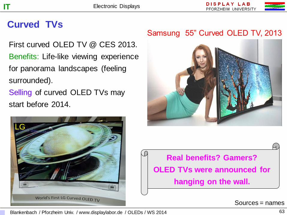
Curved TVs
63
First curved OLED TV @ CES 2013.
Benefits: Life-like viewing experience
for panorama landscapes (feeling
surrounded).
Selling of curved OLED TVs may
start before 2014.
Samsung 55” Curved OLED TV, 2013
LG
Sources = names
Real benefits? Gamers?
OLED TVs were announced for
hanging on the wall.

Electronic Displays
Blankenbach / Pforzheim Univ. / www.displaylabor.de / OLEDs / WS 2014
IT
67
OLEDs vs. LCDs : Power Consumption
OLED LCD
55” TV OLED LCD
L / cd/m² 150 – 600 > 500
Power /W 170 – 250 100 - 150
Small Size ( ~ 5“) Large Size ( ~ 55“)
Power consumption:
• Small size: POLED < PLCD
• large size: POLED 2x PLCD
Advantages of OLED?
Not latest LCD

Electronic Displays
Blankenbach / Pforzheim Univ. / www.displaylabor.de / OLEDs / WS 2014
IT
68
OLEDs vs. LCDs : Power Consumption @ 55”
Compare to 55” LCD TV
Samsung (UE55F8090) : Pwhite(250 cd/m²) 75 W (55”)
LG (55LM960V) : Pwhite(480 cd/m²) 125 W (55”)
55” curved OLED
Pwhite(250 cd/m²)
180 W (55”)
Pwhite(489 cd/m²)
252 W (55”)
For 55”
POLED 2 PLCD
OLED power
consumption
depends on
content .

Electronic Displays
Blankenbach / Pforzheim Univ. / www.displaylabor.de / OLEDs / WS 2014
IT
69
OLEDs vs. LCDs for Color AM - Displays
Polarizer
Polarizer
Glass
Glass
Colour filter
OLED / LC layer
4 vs. 1 TFT p.P.
Backlight
OLED* LCD Appr. same price
Same price ?
Lifetime, no burn in, … !
Production process costs of OLED layers ?
*: Top emitting,
white emitter

Electronic Displays
Blankenbach / Pforzheim Univ. / www.displaylabor.de / OLEDs / WS 2014
IT
70
OLED vs. LCD
OLED strengths
= LCD weaknesses
LCD improvements
(done & prototype status)
Viewing angle IPS, VA, multi-domain (all in MP)
Gamut (WLED) Quantum Dot film
Response time > 3ms, Blue Phase LC < 1 ms
Thin, light Backlight needed, but slim today
(mobile panel < 1mm, 42“ : 2,6 mm)
Efficiency (image dependent) Sequential color backlight, polarizer-free
OLED seems to be superior in some topics over LCD
but LCD has cost advantage and new approaches.
OLED drawbacks: complex TFT backplane, color, … (power for TV )

Electronic Displays
Blankenbach / Pforzheim Univ. / www.displaylabor.de / OLEDs / WS 2014
IT
71
OLEDs vs. LCDs by OLED - Manufacturer

Electronic Displays
Blankenbach / Pforzheim Univ. / www.displaylabor.de / OLEDs / WS 2014
IT
72 72
OLED Summary
• OLEDs have a short history
• Electro-optical characteristic is similar to semiconductor LEDs
• Passive Matrix OLEDs have limits in terms of resolution
• AM OLED backplane is more complex as for AM LCDs which
require however a backlight (increases thickness).
• Some small sized OLEDs are in professional applications like
- Climate control in MERCEDES E-class
- Multimeter by AGILENT
• Mass production of AM OLEDs (2013) mainly for mobile devices
• Flexible plastic (unbreakable) OLEDs may push these displays
for mobile applications.

Electronic Displays
Blankenbach / Pforzheim Univ. / www.displaylabor.de / OLEDs / WS 2014
IT
73
Summary: Technologies vs. Applications
Requirement,
Application
Suitable ?
Range Remarks
Size
Power consumption
Indoor
Outdoor
Viewing distance
Color, video
Viewing angle
Feasibility
Trends

Electronic Displays
Blankenbach / Pforzheim Univ. / www.displaylabor.de / OLEDs / WS 2014
IT
74
Summary “OLEDs”
• PM OLED is limited
in resolution like LCD.
• AM OLED backplane
is more complex than
for AM LCD (cost!).
• Some professional
PM OLEDs are
available.
• AM OLEDs are in
MP for mobile CE
products.
• OLED lifetime in app
is most important.
• Emissive display,
so negative contrast
is preferred.
0
0,2
0,4
0,6
0,8
1
0 100 200 300 400
time (hours)
Relative lu
min
an
ce
25°C
85°C
120°C
OLED