Embed Size (px)
Citation preview

Optoelectronics EE/OPE 451, OPT 444
Fall 2009 Section 1: T/Th 9:30- 10:55 PM
John D. Williams, Ph.D.
Department of Electrical and Computer Engineering
406 Optics Building - UAHuntsville, Huntsville, AL 35899
Ph. (256) 824-2898 email: [email protected]
Office Hours: Tues/Thurs 2-3PM
JDW, ECE Fall 2009
STIMULATED EMISSION DEVICES LASERS
Prentice-Hall Inc. © 2001 S.O. Kasap ISBN: 0-201-61087-6 http://photonics.usask.ca/
• 4.9 Elementary Laser Diode Characteristics • 4.10 Steady State Semiconductor Rate Equation • 4.11 Light Emitters for Optical Fiber Communications • 4.12 Single Frequency Solid State Lasers • 4.13 Quantum Well Devices • 4.14 Vertical Cavity Surface Emitting Lasers (VCSELs) • 4.15 Optical Laser Amplifiers
• Chapter 4 Homework Problems: 9-17

LED vs. Laser Diode
Typical output optical power vs. diode current (I) characteristics and the correspondingoutput spectrum of a laser diode.
Laser
LaserOptical Power
Optical Power
I0
LEDOptical Power
Ith
Spontaneous
emission
Stimulated
emission
Optical Power
© 1999 S.O. Kasap, Optoelectronics (Prentice Hall)
h Eg
Eg (b)
V
(a)
p n+
Eg
eVo
EF
p n+
Electron in CB
Hole in VB
Ec
Ev
Ec
Ev
EF
eVo
Electron energy
Distance into device
(a) The energy band diagram of a p-n+ (heavily n-type doped) junction without any bias.Built-in potential Vo prevents electrons from diffusing from n+ to p side. (b) The applied
bias reduces Vo and thereby allows electrons to diffuse, be injected, into the p-side.
Recombination around the junction and within the diffusion length of the electrons in thep-side leads to photon emission.
© 1999 S.O. Kasap, Optoelectronics (Prentice Hall)
LED Laser Diode
Typical optical power output vs. forward currentfor a LED and a laser diode.
Current0
Light powerLaser diode
LED
100 mA50 mA
5 mW
10 mW
© 1999 S.O. Kasap, Optoelectronics (Prentice Hall)

Principles of the Laser Diode
• pn junction in a Degenerate Semiconductor – Fermi level in the p region is below Ev
– Femi level in the n region is above Ec
– With no applied voltage, Efn=Efp yields a very narrow depletion region
– There is a potential energy barrier, eVo that prevents n side electrons from diffusing to the p side and vice versa
• When voltage is applied – Change in the Fermi level is the work
done by the applied voltage, eV
• If the junction is forward biased such that Efn- Efp =eV > Eg – Applied bias diminishes the build in
potential barrier
– Depletion region is no longer depleted
– There are now more electrons in the conduction band than in the valance band near Ev Population inversion
p+ n+
EF n
(a)
Eg
Ev
Ec
Ev
Ho les in V B
Electrons in C B
Junction
Electro nsE
c
p+
Eg
V
n+
(b)
EF n
eV
EF p
The energy band diagram of a degenerately doped p-n with no bias. (b) Banddiagram with a sufficiently large forward bias to cause population inversion andhence stimulated emission.
Inv ers io nreg io n
EF p
Ec
Ec
eVo
© 1999 S.O. Kasap, Optoelectronics (Prentice Hall)

Principles of the Laser Diode
• Population inversion region is a layer along the junction called the inversion layer (active region)
• An incoming photon with energy Ec-Ev cannot excite an electron in Ev to Ec as there are hardly any present in the valance band within the active region
• Hence there is more stimulated emission than absorption
• The optical gain present in the active region due to lack of probability of valance electron absorption
h
Eg
Optical gainE
F n E
F p
Optical absorption
0
Energy
Ec
Ev
CB
VB
(a) The density of states and energy distribution of electrons and holes inthe conduction and valence bands respectively at T 0 in the SCLunder forward bias such that EFn EFp > Eg. Holes in the VB are emptystates. (b) Gain vs. photon energy.
Density of states
Electrons
in CB
Holes in VB
= Empty states
EF n
EF p
eV
At T > 0
At T = 0
(a) (b)
© 1999 S.O. Kasap, Optoelectronics (Prentice Hall)
Photonics, 6th edition Yariv and Yeh 6
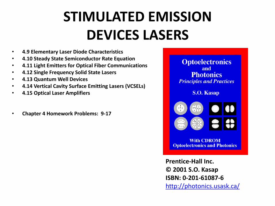
Figure 15.5 An optical beam at w0 with intensity I(w0) is incident on a pumped semiconductor medium characterized by quasi-Fermi levels EFc and EFs.
A single level pair a b with the same k value is shown. The induced transition a b contributes one photon to the beam.
Cc 2007 Photonics, 6th edition Yariv and Yeh (Oxford University Press

Electro-optical Performance of III/V Diodes
• injection pumping: Optical pumping is achieved by forward diode current and the pumping energy is an external battery
• For laser we also need an optical resonator cavity. This is achieved through the use of a slab waveguide with a high index contrast at the emission end
• Wavelength of the radiation that can build up in the cavity depends on the length (L) in half multiples
LElectrode
Current
GaAs
GaAsn+
p+
Cleaved surface mirror
Electrode
Act ive region(stimulated emission region)
A schematic illustration of a GaAs homojunction laserdiode. The c leaved surfaces ac t as reflecting mirrors.
L
© 1999 S.O. Kasap, Optoelectronics (Prentice Hall)
Typical output optical power vs. diode current (I) characteristics and the correspondingoutput spectrum of a laser diode.
Laser
LaserOptical Power
Optical Power
I0
LEDOptical Power
Ith
Spontaneous
emission
Stimulated
emission
Optical Power
© 1999 S.O. Kasap, Optoelectronics (Prentice Hall)
• 2 critical current identifiers
• Transparency current: Current above which no net photon absorption occurs
• Threshold current: current above which optical gain overcomes all photon losses in the cavity
Ln
m 2

Heterojunction Laser Diodes
• Main issue with homojunction diodes is that the laser threshold current density is too high for practical uses. – Ex. Jth = 500A/mm2 for GaAs at 300K
• Heterostructured diodes reduce these current densities by orders of magnitude
• This is achieved through a combination of carrier confinement (mismatched materials), and photon confinement (geometric shape of the waveguide)
• Double heterojunction (DH) devices with npp layers allow for designed confinement of the active region
• Lower refractive index of the AlGaAs enhances the mode confinement in comparison to a homo or simple heterojunction device
• Significantly reduces threshold current density
Refractiveindex
Photondensity
Active
region
n ~ 5%
2 eV
Holes in VB
Electrons in CB
AlGaAsAlGaAs
1.4 eV
Ec
Ev
Ec
Ev
(a)
(b)
pn p
Ec
(a) A doubleheterostructure diode hastwo junctions which arebetween two differentbandgap semiconductors(GaAs and AlGaAs).
2 eV
(b) Simplified energyband diagram under alarge forward bias.Lasing recombinationtakes place in the p-GaAs layer, theactive layer
(~0.1 m)
(c) Higher bandgapmaterials have alower refractiveindex
(d) AlGaAs layersprovide lateral opticalconfinement.
(c)
(d)
© 1999 S.O. Kasap, Optoelectronics (Prentice Hall)
GaAs

Edge Emitting Lasers
• Very similar to ELED devices presented in chapter 3
• Additional contacting layer of p-GaAs next to the p=AlGaAs provides better contacting and avoids Schottky junction which would limit the current in the device.
• p- and n- AlGaAs layers provide carrier and optical confinement in the vertical direction
• Laser emission in the active p-GaAs(or a different AlGaAs constitution) region is between 870-900 nm depending on doping.
Schematic illustratio n of the the st ruct ure of a double heterojunction st ripecontact laser diode
Oxide insulator
Stripe electrode
Subst rateElectrode
Active region where J > Jth.
(Emission region)
p-GaAs (Contacting lay er)
n-GaAs (Substrate)
p-GaAs (Active lay er)
Current
pa ths
L
W
Cleaved reflecting surfaceElliptic al
laser
be am
p-AlxGa
1-xAs (Confining lay er)
n-AlxGa
1-xAs (Confining lay er)
12 3
Cleaved reflecting surface
Substrate
© 1999 S.O. Kasap, Optoelectronics (Prentice Hall)
• AlGaAs and GaAs have negligible lattice mismatch yielding very few defects in the crystal that would lead to excessive threshold currents
• Also, the stripe electrode across the top confines the electric field and thus the optically active region providing additional geometrical confinement
• Such lasers are called gain guided, b/c the current density generated is guided by the electric field between the stripe electrode and the bottom electrode

Photonics, 6th edition Yariv and Yeh
Figure 15.10 A typical double heterostructure GaAs/GaAlAs laser. Electrons and holes are injected into the active GaAs layer from the
n and p GaAlAs. Photons with frequencies near nEg/h are amplified by stimulating electron–hole recombination.
Cc 2007 Photonics, 6th edition Yariv and Yeh (Oxford University Press

Photonics, 6th edition Yariv and Yeh
11
Figure 15.12 The magnitude of the energy gap in Ga1x Alx As as a function of the molar fraction x. For x >0.37 the bandgap is indirect.
(After Reference [11].)
Cc 2007 Photonics, 6th edition Yariv and Yeh (Oxford University Press
Photonics, 6th edition Yariv and Yeh
12
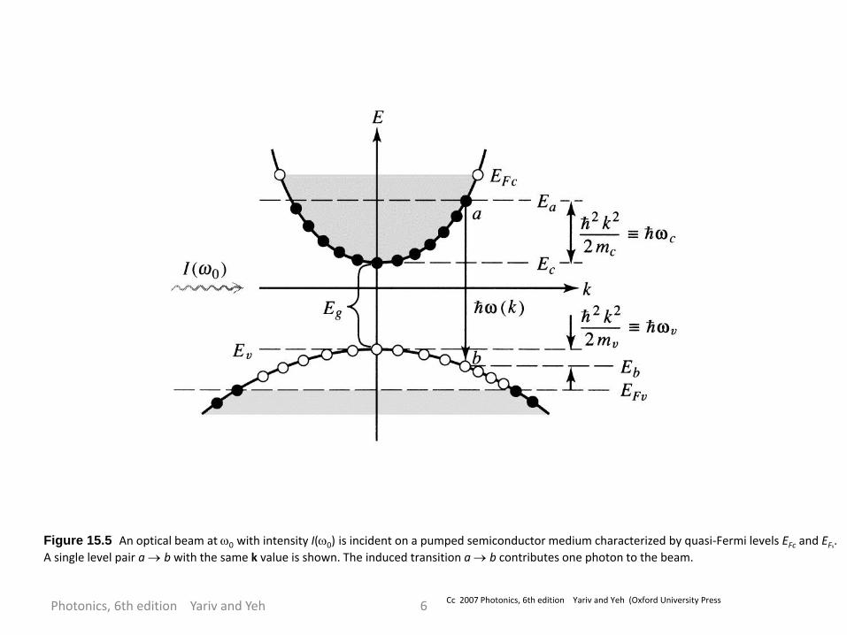
Figure 15.15 III–V compounds: lattice constants versus energy bandgaps and corresponding wavelengths. The solid lines correspond to direct-gap materials and the dashed lines to in-direct-gap materials. The binary-compound substrates that can be used for lattice-matched growth are indicated on the right. (After Reference [11].)
Cc 2007 Photonics, 6th edition Yariv and Yeh (Oxford University Press

Buried Heterostructure LDs
Figure from Chapter 15 Photonics, 6th edition Yariv and Yeh 2007 Oxford University Press
• Although the stripe electrode geometry provides some geometric confinement, it is more advantageous to restrict lateral geometry physically through the use of confining layers along the side of the diode
• Creation of a optical waveguide in both vertical and horizontal directions aids in reducing optical cavity modes and promotes confinement
• Significantly reduces current density required for stimulated emission

Example: Modes in a laser and the Optical Cavity length
• AlGaAs heterojunction LD with cavity length of 200 um and radiation peak of 870 nm.
• What is the mode integer of the peak radiation and the separation between modes in the cavity.
• If the optical gain vs wavelength characteristics has a FWHM wavelength of 6nm, how many modes are there within this bandwidth?
• How many modes are there if the cavity has a length of 20 um?
mestwoofSeparation
spectrumofLinewidthModes
m
2
1
mod___
__
Optical gain between
FWHM pointsm
(a) 5 modes
(b)4 modes
Number of laser modesdepends on how thecavity modes intersectthe optical gain curve.In this case we arelooking at modeswithin the linewidth1.
Cavity modes
© 1999 S.O. Kasap, Optoelectronics (Prentice Hall)
1 mode corresponding to 900 nm. In fact, m must be an integer and when m = 1644 and lamda = 902/4 nm. It is apparent that reducing the cavity suppress higher order modes
esnm
nm
nm
mL
nLm
nL
m
nL
m
nL
nLm
Ln
m
m
m
m
mod10547.0
6
547.0)10200)(7.3(2
)10900(
10200
2
2
1
22
1644)10900(
)10200)(7.3(22
2
21
6
29
6
2
2
9
6
1.1
47.5)1020)(7.3(2
)10900(
1020
21
6
29
6
m
m nm
mL

Elementary Laser Diode (LD) Characteristics
• Longitudinal mode: length determined
• Lateral mode: width determined
• Emission is either multimode or single mode depending on the optical resonating structure and the pumping current level
Height, HWidth W
Length, L
The laser cavity definitions and the output laser beamcharacteristics.
Fabry-Perot cavity
Dielectric mirror
Diffraction
limited laser
beam
© 1999 S.O. Kasap, Optoelectronics (Prentice Hall)
778 780 782
Po = 1 mW
Po = 5 mW
Relative optical power
(nm)
Po = 3 mW
Output spectra of lasing emission from an index guided LD.At sufficiently high diode currents corresponding to highoptical power, the operation becomes single mode. (Note:Relative power scale applies to each spectrum individually andnot between spectra)
© 1999 S.O. Kasap, Optoelectronics (Prentice Hall)

Laser Performance as a Function of Temperature
• Output spectrum and mode properties are temperature dependant
• Single mode LDs exhibit a mode hop at certain temperatures corresponding to a change in peak emission wavelength
• Nominal wavelength of the laser increases slowly between hops due to change in refractive index, n, with temperature
• Slope efficiency determines laser efficiency and is not the same as LED conversion efficiency stated in chapter 3.
0 20 40 60 80
0
2
4
6
8
10
Po (mW)
I (mA)
0 C
25 C
50 C
Output optical power vs. diode current as three different temperatures. Thethreshold current shifts to higher temperatures.
© 1999 S.O. Kasap, Optoelectronics (Prentice Hall)
th
oslope
II
P

Example: Laser Output Wavelength Variations
• Given: Refractive index, n, of GaAs has a temp dependence dn/dT 1.5 x 10⁻⁴K-1
• Estimate the change in emitted wavelength from 870 nm per degree change in temp between mode hops
K
nmK
nm
dT
dn
ndT
d
dT
dn
m
L
m
Ln
dT
d
dT
d
Ln
m
mm
m
m
035.0105.17.3
870
22
2
14
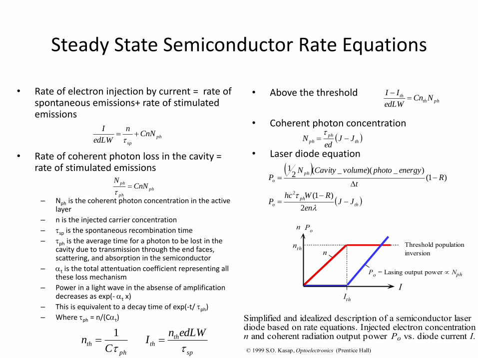
Steady State Semiconductor Rate Equations
• Rate of electron injection by current = rate of spontaneous emissions+ rate of stimulated emissions
• Rate of coherent photon loss in the cavity = rate of stimulated emissions
– Nph is the coherent photon concentration in the active layer
– n is the injected carrier concentration
– sp is the spontaneous recombination time
– ph is the average time for a photon to be lost in the cavity due to transmission through the end faces, scattering, and absorption in the semiconductor
– t is the total attentuation coefficient representing all these loss mechanism
– Power in a light wave in the absense of amplification decreases as exp(- t x)
– This is equivalent to a decay time of exp(-t/ ph)
– Where ph = n/(Ct) Simplified and idealized description of a semiconductor laserdiode based on rate equations. Injected electron concentrationn and coherent radiation output power Po vs. diode current I.
IIth
nth
n
nThreshold population
inversion
Po
Po = Lasing output power Nph
© 1999 S.O. Kasap, Optoelectronics (Prentice Hall)
ph
sp
CnNn
edLW
I
ph
ph
phCnN
N
sp
thth
edLWnI
• Above the threshold
• Coherent photon concentration
• Laser diode equation
phthth NCn
edLW
II
ph
thC
n
1
th
ph
ph JJed
N
th
ph
o
ph
o
JJen
RWhcP
Rt
energyphotovolumeCavityNP
2
)1(
)1()_)(_(
21
2

Light Emitters for Optical Fiber Communications
• Choice of light source depends on communication distance and bandwidth required
• For short haul applications, such as local networks, LEDs are preferred because they are simpler to drive, cheaper to produce, have a longer lifetime, and provide the necessary output power even though the output spectrum is broader
• LEDs are used in multimode and graded index fibers b/c the dispersion arising from finite linewidth of the output spectrum is not a major concern
• For long haul and wide bandwidth communications, Laser diodes are used because of their narrow linewidth and high output power.
• Output spectrum of a laser diode can be very narrow (0.01 nm – 0.1 nm)
• Very fast operation defined by the rise time associated with inversion in a laser diode make it more amenable for high speed applications even when wide bandwidths are required.
Typical optical power output vs. forward currentfor a LED and a laser diode.
Current0
Light powerLaser diode
LED
100 mA50 mA
5 mW
10 mW
© 1999 S.O. Kasap, Optoelectronics (Prentice Hall)

Distributed Bragg Reflection for Single Mode Lasers
• Ensure single mode radiation in the laser cavity is to use frequency selective mirrors at the cleaved surfaces
• Distributed Bragg reflector is a mirror that has been designed a reflective Bragg grating
• Reflected wave occurs only when the wavelength corresponds to twice the corrugation periodicity, .
• The diffraction order of the reflector is integer, q = 0,1,2,…
• N = refractive index of the mirror
• Bragg wavelength of the mirror output is B
Corrugated
dielectric structure
Distributed Bragg
reflector
(a) (b)
A
B
q(B/2n) =
Active layer
(a) Distributed Bragg reflection (DBR) laser principle. (b) Partially reflected wavesat the corrugations can only constitute a reflected wave when the wavelengthsatisfies the Bragg condition. Reflected waves A and B interfere constructive when
q(B/2n) = .
© 1999 S.O. Kasap, Optoelectronics (Prentice Hall)
2n
q B
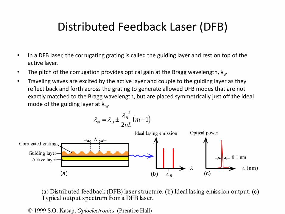
Distributed Feedback Laser (DFB)
• In a DFB laser, the corrugating grating is called the guiding layer and rest on top of the active layer.
• The pitch of the corrugation provides optical gain at the Bragg wavelength, λB.
• Traveling waves are excited by the active layer and couple to the guiding layer as they reflect back and forth across the grating to generate allowed DFB modes that are not exactly matched to the Bragg wavelength, but are placed symmetrically just off the ideal mode of the guiding layer at λm.
Active layer
Corrugated grating
Guiding layer
(a)
(a) Distributed feedback (DFB) laser structure. (b) Ideal lasing emission output. (c)Typical output spectrum from a DFB laser.
Optical power
(nm)
0.1 nm
Ideal lasing emission
B(b) (c)
© 1999 S.O. Kasap, Optoelectronics (Prentice Hall)
12
2
mnL
BBm

DFB Laser Example
• Consider a DFB laser that has a corrugation period of = 0.22 m and a grating length, L, of 400 microns.
• Suppose that the effective refractive index of the medium is 3.5.
• Assume a first order grating and calculate the Bragg wavelength, the mode wavelengths, and their separation
Bragg wavelength
Symmetric mode wavelengths
Wavelengths are separated by 1.7 nm. Due to some symmetry, only one mode will appear in the output and for the most practicle purposes the mode wavelength can be taken as B.
mm
q
nB
54.1
1
)5.3)(22.0(22
morm
m
mmm
nL
BBm
5408.1______5392.1
)10()400)(5.3(2
54.154.11
2
0
22

Cleaved Coupled Cavity Laser
• Device has two different optical cavities of length L and D.
• Each laser cavity is pumped by a different current
• Only modes resonant in both cavities are allowed to resonate through the entire device, allowing the engineer to tune out certain modes from one or both independent laser diodes
• Why pump both the cavities? Ans. Allowed modes in an unpumped cavity will undergo recombination if the device is not driven.
Active
layer
L D
(a)
Cleaved-coupled-cavity (C3) laser
Cavity Modes
In L
In D
In both
L and D
(b)
© 1999 S.O. Kasap, Optoelectronics (Prentice Hall)
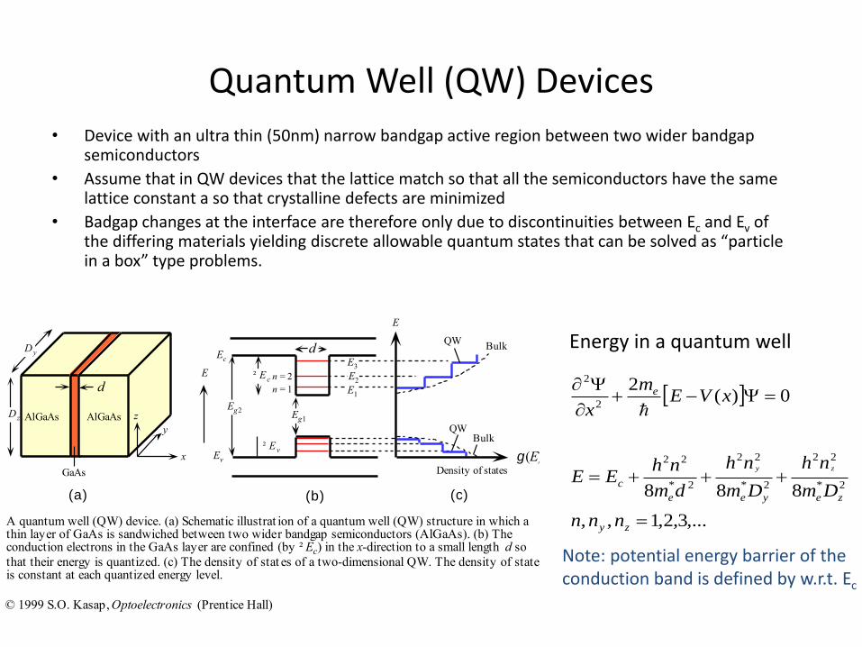
Quantum Well (QW) Devices
• Device with an ultra thin (50nm) narrow bandgap active region between two wider bandgap semiconductors
• Assume that in QW devices that the lattice match so that all the semiconductors have the same lattice constant a so that crystalline defects are minimized
• Badgap changes at the interface are therefore only due to discontinuities between Ec and Ev of the differing materials yielding discrete allowable quantum states that can be solved as “particle in a box” type problems.
A quantum well (QW) device. (a) Schematic illustrat ion of a quantum well (QW) structure in which athin layer of GaAs is sandwiched between two wider bandgap semiconductors (AlGaAs). (b) Theconduction electrons in the GaAs layer are confined (by ² Ec) in the x-direction to a small length d so
that their energy is quantized. (c) The density of stat es of a two-dimensional QW. The density of statesis constant at each quantized energy level.
AlGaAs AlGaAs
GaAs
y
z
x
d
Ec
Ev
d
E1
E2
E3
g(E)Density of states
E
BulkQW
n = 1
Eg2Eg1
E n = 2² Ec
BulkQW
² Ev
(a) (b) (c)
Dy
Dz
© 1999 S.O. Kasap, Optoelectronics (Prentice Hall)
,...3,2,1,,
888
0)(2
2*
22
2*
22
2*
22
2
2
zy
zeyee
c
e
nnn
Dm
nh
Dm
nh
dm
nhEE
xVEm
x
zy
Note: potential energy barrier of the conduction band is defined by w.r.t. Ec
Energy in a quantum well

Different Quantum Wells Types Based on Geometry
Image from Chapter 16, of Fundamentals of Photonics, 2nd ed. By Saleh and Teich cc 2007 Wiley Interscience

Density of States from our Particle in a Box Solution (QW Device)
Figure from Chapter 16 Photonics, 6th edition Yariv and Yeh 2007 Oxford University Press

Energy Spectrum in a Quantum Well (SQW)
E
c
Ev
E1
E1
h = E1 – E
1
E
In single quantum well (SQW) lasers electrons areinjected by the forward current into the thin GaAslayer which serves as the active layer. Populationinversion between E1 and E1 is reached even with a
small forward current which results in stimulatedemissions.
© 1999 S.O. Kasap, Optoelectronics (Prentice Hall)

Example: A GaAs QW
• GaAs QW
• Effective electron mass is me*=0.07me
• What are the first two electron energy levels for a QW of thickness 10 nm?
• What is the hole energy below Ev if the effective electron mass of the hole, mh* = .5me?
• What is the emission wavelength w.r.t. bulk GaAs which as an energy bandgap of 1.42 eV?
• Difference in emission wavelength between a bulk GaAs LD and a QW LD is 35 nm
Figure 16.1 The layered structure and the bandedges of a GaAlAs/GaAs/GaAlAs quantum well.
Cc 2007 Photonics, 6th edition Yariv and Yeh (Oxford University Press
nm
eV
nmeV
E
hc
nmeV
nmeV
E
hc
eVdm
nh
eVdm
nh
nng
QW
g
g
h
n
e
n
8390075.00527.042.1
1240
87442.1
1240
0075.08
0537.08
'
2*
22'
2*
22

Multiple Quantum Well (MQW) Lasers
Active layer Barrier layer
Ec
Ev
E
A multiple quantum well (MQW) structure.Electrons are injected by the forward currentinto active layers which are quantum wells.
© 1999 S.O. Kasap, Optoelectronics (Prentice Hall)
Image from Chapter 16, of Fundamentals of Photonics, 2nd ed. By Saleh and Teich cc 2007 Wiley Interscience
• Discrete states in MQW devices that have thick barrier layers generate increased optical intensity at the same wavelength predicted by SQW devices
• However if the barrier layer thickness is very thin (10 – 20 nm or so) then tunneling of quantum states between barriers provides coupling mechanisms that must be accounted for
• Tunneling allows for the production of minibands within the bound quantum DOS. These minibands are the spread of the of the single quantum band that allows for electron energies to spread due to interactions between isolated quantum energy states within each active layer

Quantum Mechanical Tunneling • Truly quantum phenomenon
• States that a quantum wave has a finite probability of passing through an infinite potential barrier into a neighboring state
• The transmission of the wave exponentially decays with distance and the size of the barrier potential
• For QW devices, the barrier potential is the difference between the conduction or valance band peaks between the active and cladding regions of the diode junction
• The potential difference in AlGaAs/GaAs devices is
Vo = EcAlGaAs-EcGaAs 0.3 eV
• Results of tunneling produce a smearing of energy states available in MQW devices
)2exp(116
)(8
18
)exp()exp()(
)exp()exp()(
)exp()exp()(
0)(2
2
2
2
2
1
33333
22222
11111
2
2
aKV
E
V
ET
EVh
mK
mh
mEK
xjKBxjKAx
xKBxKAx
xjKBxjKAx
xVEm
x
oo
o
e
V(x)
Vo
Region I Region II Region III
x =0 x = a
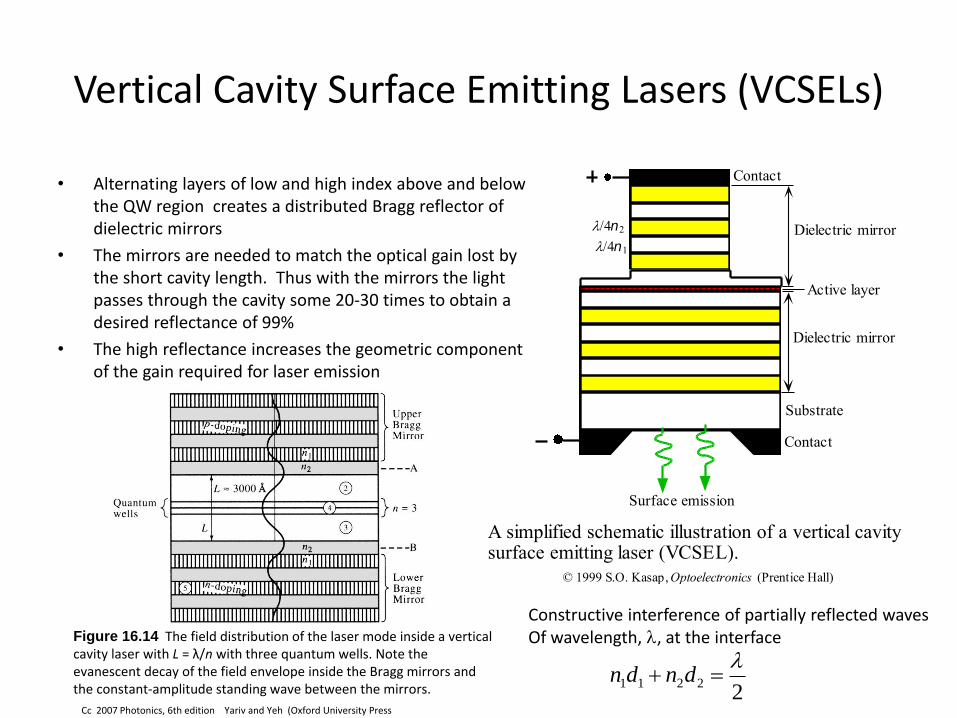
Vertical Cavity Surface Emitting Lasers (VCSELs)
• Alternating layers of low and high index above and below the QW region creates a distributed Bragg reflector of dielectric mirrors
• The mirrors are needed to match the optical gain lost by the short cavity length. Thus with the mirrors the light passes through the cavity some 20-30 times to obtain a desired reflectance of 99%
• The high reflectance increases the geometric component of the gain required for laser emission
A simplified schematic illustration of a vertical cavitysurface emitting laser (VCSEL).
Contact
Surface emission
Dielectric mirror
Contact
Substrate
/4n1
Active layer
/4n2 Dielectric mirror
© 1999 S.O. Kasap, Optoelectronics (Prentice Hall)
Figure 16.14 The field distribution of the laser mode inside a vertical cavity laser with L = λ/n with three quantum wells. Note the evanescent decay of the field envelope inside the Bragg mirrors and the constant-amplitude standing wave between the mirrors.
Cc 2007 Photonics, 6th edition Yariv and Yeh (Oxford University Press
22211
dndn
Constructive interference of partially reflected waves Of wavelength, , at the interface
VCSEL Attributes
• VCSEL active layers are generally very thin – 0.1 um and comprised of MQW for improved threshold current
• The device is comprised of epitaxially deposited layer on a suitable substrate which is transparent in the emission wavelength
• Ex. 980 nm VCSEL devices – InGaAs is the active layer – GaAs is the substrate – AlGaAs with different compositions comprise the dielectric mirror stack – The top stack is then etched after all the layers have been deposited to create the inverted T shape
presented in the previous slide • In practice, current flowing through the dielectric mirrors gives rise to an undesired voltage drop that
makes the device VERY sensitive to failure from electrostatic discharge. In fact, this is the most common failure mode during VCSEL operation and installation.
• The vertical cavity and thus the emitted beam is generally circular in cross section • The height of the vertical cavity is several microns. Thus the longitudinal mode separation is sufficiently
large to allow only one mode of operation. However lateral modes may be present in certain cavity geometries
• In practice VCSELS have several lateral modes but the spectral width is only ½ nm which is substantially less than the longitudinal modes of a DFB or ELD.
• Also, VCSELS have an average beam divergence of about 8-12o depending on their fabrication and materials used
• Dual wavelength VCSEL emission is obtained by operating at high currents.
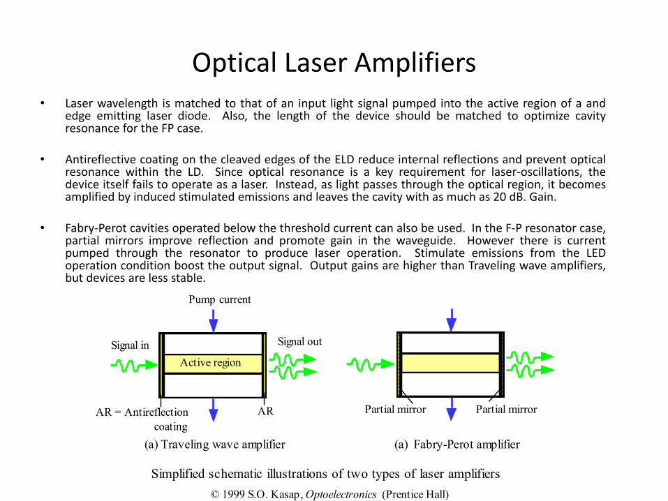
Optical Laser Amplifiers • Laser wavelength is matched to that of an input light signal pumped into the active region of a and
edge emitting laser diode. Also, the length of the device should be matched to optimize cavity resonance for the FP case.
• Antireflective coating on the cleaved edges of the ELD reduce internal reflections and prevent optical resonance within the LD. Since optical resonance is a key requirement for laser-oscillations, the device itself fails to operate as a laser. Instead, as light passes through the optical region, it becomes amplified by induced stimulated emissions and leaves the cavity with as much as 20 dB. Gain.
• Fabry-Perot cavities operated below the threshold current can also be used. In the F-P resonator case,
partial mirrors improve reflection and promote gain in the waveguide. However there is current pumped through the resonator to produce laser operation. Stimulate emissions from the LED operation condition boost the output signal. Output gains are higher than Traveling wave amplifiers, but devices are less stable.
Simplified schematic illustrations of two types of laser amplifiers
Pump current
Active region
AR = Antireflection
coating
AR
Signal in Signal out
(a) Traveling wave amplifier (a) Fabry-Perot amplifier
Partial mirror Partial mirror
© 1999 S.O. Kasap, Optoelectronics (Prentice Hall)
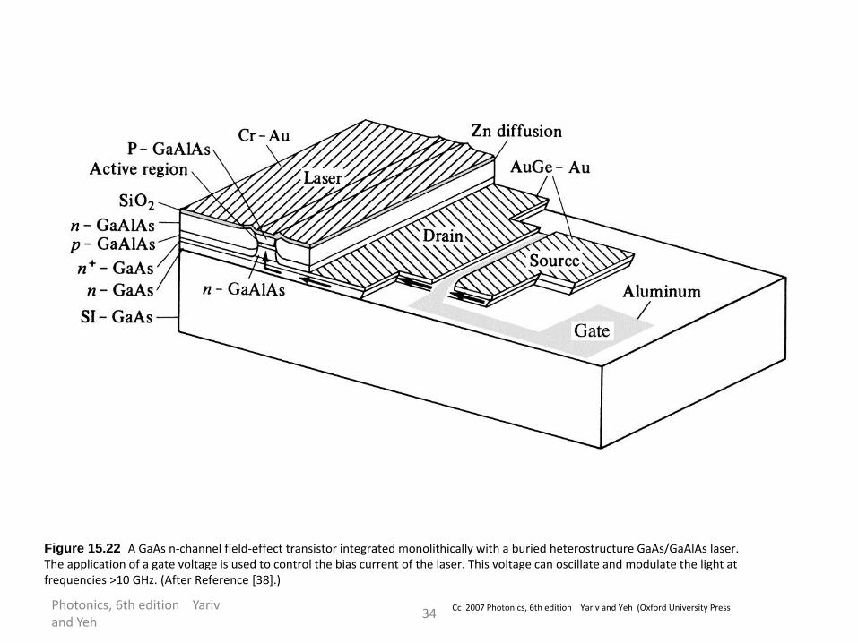
Photonics, 6th edition Yariv and Yeh
34
Figure 15.22 A GaAs n-channel field-effect transistor integrated monolithically with a buried heterostructure GaAs/GaAlAs laser. The application of a gate voltage is used to control the bias current of the laser. This voltage can oscillate and modulate the light at frequencies >10 GHz. (After Reference [38].)
Cc 2007 Photonics, 6th edition Yariv and Yeh (Oxford University Press

Photonics, 6th edition Yariv and Yeh
35
Figure 15.23 A monolithically integrated optoelectronic repeater containing a detector, transistor current source, a FET amplifier, and a laser on a single-crystal GaAs substrate. (After Reference [39].)
Cc 2007 Photonics, 6th edition Yariv and Yeh (Oxford University Press

Photonics, 6th edition Yariv and Yeh
36
Figure 15.24 A monolithic circuit containing a tunable multisection InGaAsP/InP 1.55 m laser employing multiquantum well (MQW) gain section, a passive waveguide for an external input optical wave, and a directional coupler switch for combining the laser output field and that of the external input at the output ports. (After Reference [41].)
Cc 2007 Photonics, 6th edition Yariv and Yeh (Oxford University Press

Photonics, 6th edition Yariv and Yeh
37
Figure 15.25 An optoelectronic integrated circuit composed of three ~1.5 m InGaAs/InP distributed feedback lasers each tuned to a slightly different wavelength. The three wavelengths are fed into a single waveguide and amplified in a single amplifying section. (After Reference [42].)
Cc 2007 Photonics, 6th edition Yariv and Yeh (Oxford University Press