Embed Size (px)
Citation preview

University of South FloridaScholar Commons
Graduate Theses and Dissertations Graduate School
11-2-2010
Optical Design of Beam Shaping Optics forCamera Probe and LED Light Illumination Usedfor Minimally Invasive Abdominal SurgeryWeiyi HeUniversity of South Florida
Follow this and additional works at: http://scholarcommons.usf.edu/etd
Part of the American Studies Commons, and the Physics Commons
This Thesis is brought to you for free and open access by the Graduate School at Scholar Commons. It has been accepted for inclusion in GraduateTheses and Dissertations by an authorized administrator of Scholar Commons. For more information, please contact [email protected].
Scholar Commons CitationHe, Weiyi, "Optical Design of Beam Shaping Optics for Camera Probe and LED Light Illumination Used for Minimally InvasiveAbdominal Surgery" (2010). Graduate Theses and Dissertations.http://scholarcommons.usf.edu/etd/3532

Optical Design of Beam Shaping Optics for Camera Probe and LED Light
Illumination Used for Minimally Invasive Abdominal Surgery
By
Weiyi He
A thesis submitted in partial fulfillment of the requirement for the degree of
Master of Science Department of Physics
College of Arts and Sciences University of South Florida
Major Professor: Dennis K. Killinger, Ph.D. Myung K.Kim, Ph.D Dale Johnson, Ph.D
Date of Approval November 2, 2010
Keywords: LED illuminator, Optical reflectors, Beam shaping, Intensity distribution, Ray tracing simulation, CMOS/CCD camera and lens
Copyright©2010, Weiyi He

ACKNOWLEDGEMENTS
I would like to express my deepest appreciation to Dr. Killinger for his support and
invaluable guidance during this project, especially for all the painful editions of this
thesis he went through. I would also like to express my thanks to Dr. Johnson and Dr.
Kim for serving on my thesis committee. I would like to thank Dr. Richard Gitlin,
Adam Anderson, Yu Sun , MS student Cristian Castro, and BS student Sara Smith
from the Department of Electrical Engineering , University of South Florida, for the
collaboration work and exchange of information and reference materials. I would like
to thank Mr. Pete Savage for his cone reflector samples and valuable advice on
experiments and designs. And lastly I would like to thank REU student Susanna
Todaro for conducting the early model simulation work. Also, I am greatly thankful to
the Lambda Research Corporation who expanded my TracePro60’s 30-days trial use
to half a year.

TABLE OF CONTENTS LIST OF TABLES iii LIST OF FIGURES iv ABSTRACT vii CHAPTER 1. INTRODUCATION 1 CHAPTER 2. CURRENT MEDICAL RESEARCH IN IMPLANTABLE DEVICE 6
2.1 Previous work on insertable surgical camera probe and LED lighting device. 6
2.2 Example of optical design of reflectors 10 CHAPTER 3. EXPERIMENTAL MEASUREMENT 13
3.1 Experimental Setup and Apparatus 13
3.2 LED/photodiode parameters 14 CHAPTER 4. INITIAL SIMULATIONS USING TRACEPRO RAY TRACING SOFTWARE 30 4.1 TracePro Software 30 4.2 Initial simulations using TracePro 34 CHAPTER 5. PREDICTED INTENSITY ANGULAR DISTRIBUTION USING RAY TRACING PROGRAM 38
5.1 Initial geometry of LED, half-sphere holders, and parabola reflectors 38
i

5.2 Different optical reflector geometries 41
CHAPTER 6. PREDICTED INTENSITY PROFILES USING TRACEPRO 53 CHAPTER 7. INITIAL OPTICAL DESIGN FOR CCD CAMERA 64 CHAPTER 8. CONCLUSION AND FUTURE WORK 70 REFERENCES 71 APPENDICES 72
Appendix A: Early Poster Presentation at REU/USF Summer Conference 73
ii

LIST OF TABLES
Table 3.1 Electro-optical properties of LED. 17 Table 3.2 Typical electro-optical specifications at T=23oC for Si photodiode PIN SC/10D. 20 Table 3.3 CCD datasheet of Model OV 6930. 28 Table 6.1 Maximum intensity value for different reflectors at different Distances. 63
iii

LIST OF FIGURES Figure 1.1 Model of the proposed medical probe. 2 Figure 2.1 Implemented Prototype device with LED lighting and pan/tilt axes. 7 Figure 2.2 Photo of LED assemblies. Left: CAD layout of LEDs. Right: LED board and LED. 8 Figure 2.3 Photo of CCD camera and lens assemblies. 9 Figure 2.4 Example of optical reflector used to enhance intensity from LED lamp. 11 Figure 3.1 Schematic of LED light distribution experiment. 15 Figure 3.2 Photograph of the triple LED (green). 16 Figure 3.3 Photograph of photodiode. 18 Figure 3.4 Spectral response for Si photodiode .Model PIN SC/10D. 19 Figure3.5 Photograph of aluminium foil cone reflectors with different half
angle ,from left to right: 10o, 20o ,30o. 22 Figure 3.6 Photograph of LED (green) with cone reflector made of aluminium foil. 23 Figure 3.7 Photograph of the laboratory system used to measure angular dependence of LED optical output. 24 Figure 3.8 Measured LED light distribution using different light reflecting cones; distance was 2cm. 26 Figure 3.9 Measured LED light distribution using different light reflecting cones; distance was 5cm. 27 Figure 3.10 CCD Camera images of drawing on paper target. 29 Figure 4.1 Elliptical lamp design using TracePro software. 32
iv

Figure 4.2 Blue LED excitation and yellow luminescence rays propagating through 3-D solid model in TracePro. 33
Figure 4.3 Geometry of LED light distribution experimental model in TracePro software. 35 Figure 4.4 Predicted LED light distribution using TracePro software when LED distance is 2 cm 36 Figure 4.5 Predicted LED light distribution using TracePro software when LED distance is 5 cm 37 Figure 5.1 Design of LED base within spherical well. 39 Figure 5.2 Cross-section view of LED base for parabolic reflector. 40 Figure 5.3 CAD drawing of three reflector geometries showing. 42 Figure 5.4 LED ring with individual reflectors showing predicted optical ray tracing. 43 Figure 5.5 Fraction of the emitted rays that hit the +/- 45o Calculation Limit Area as a function of the half angle of reflector. 45 Figure 5.6 Fraction of the emitted rays that hit the +/- 45o Calculation Limit Area as function of the focal length. 47 Figure 5.7 Fraction of rays that hit the +/- 45o Calculation Limit Area as a function of z position of LEDs within the half-spherical wells of the 20o cone reflector design. 48 Figure 5.8 Cone reflector intensity distribution simulation. Number of rays for 1 cm2 on 5cm away +/- 45o Calculation Limit Area as function of half-angle of cone reflector. 49 Figure 5.9 Parabolic reflector intensity distribution simulation. Number of rays for 1cm2 on 5cm away +/- 45o Calculation Limit Area as function of focal length of parabolic reflector. 50 Figure 5.10 Collar reflector intensity distribution simulation. Number of rays for 1cm2 on 5cm away +/- 45o Calculation Limit Area as function of half-angle of collar reflector. 51
v

Figure 6.1 LED light pattern simulation (no reflector; absolute intensity), measured at distance of 0 cm, 2 cm, and 5 cm from the LED Source (top to bottom). 54 Figure 6.2 LED light pattern simulation (no reflector; relative intensity), measured at distance of 0 cm, 2 cm, and 5 cm from the LED Source. 55 Figure 6.3 LED light pattern simulation (20ocone reflector; absolute intensity), measured at distances of 0 cm, 2cm, and 5cm from the LED sources. 56 Figure 6.4 LED light pattern simulation (20o cone reflector; relative intensity), measured at distances of 0 cm, 2cm, and 5cm from the LED sources. 57 Figure 6.5 LED light pattern simulation (f=0.4mm parabolic reflector; absolute
intensity), measured at distances of 0 cm, 2cm ,and 5 cm from the LED sources ( top to bottom). 58 Figure 6.6 LED light pattern simulation (f=0.4mm parabolic reflector; relative Intensity), measured at distances of 0 cm, 2cm ,and 5 cm from the LED sources (top to bottom). 59 Figure 6.7 LED light pattern simulation (17.5o collar reflector; absolute intensity), measured at distance of 0 cm, 2 cm, and 5 cm from the LED sources (top to bottom). 60 Figure 6.8 LED light pattern simulation (17.5o collar reflector; relative intensity), measured at distance of 0 cm, 2 cm, and 5 cm from the LED sources (top to bottom). 61 Figure 7.1 Schematic diagram of Lens and CCD system. 65 Figure 7.2 Datasheet of CMOS 67 Figure 7.3 Parameters of the desired lens configuration. 68 Figure A.1 Early Poster Presentation at REU/USF Summer Conference 73
vi

vii
ABSTRACT
The optical design of a LED illuminator and camera imaging system were
studied for potential use in a small medical "robotic type" probe to be used for
minimally invasive abdominal surgery. Beam shaping optical reflectors were studied
to increase the intensity distribution of the LED beam directed toward a close-by
target surface. A CMOS/CCD camera and lens was used to image the targeted area.
In addition, extensive optical ray tracing simulations were made to predict the
intensity patterns. The experimental measurements and ray tracing simulations were
in good agreement, and indicated that 20 degree cone reflectors for the LED sources
and appropriate micro-lens/CCD chip imaging optics should provide a useful image at
a working distance of about 5 cm.

CHAPTER 1. INTRODUCTION
Minimally invasive techniques are becoming more and more important in the
field of abdominal surgery and often use traditional endoscopes to insert surgical tools
and observation paths into the body. Traditional endoscopes often use optical fibers
to deliver the light into the abdomen and a fiber-lens to transmit the image back to a
CCD camera sensor. In the specific case of minimally invasive abdominal surgery,
surgeons first make one incision through the abdominal wall (usually the belly-
button) , then they insert a trocar into the incision, which has space for four objects: a
CO2 source, to inflate the abdominal cavity, a high intensity light source to illuminate
the cavity, a video detector and cable, and one surgical instrument.1 This use of only
one surgical instrument is highly limiting, as it limits the type and scope of operations
that can be performed. As a result, there is a need to develop devices that can help
increase the number of surgical instruments that can be used through the opening,
without hindering the other viewing and illumination capabilities.
Toward this end, several research groups have conducted research to come up
with better ideas for either an endoscope system or different light illuminating and
video imaging devices. As an example, Dr Tie Hu’s research group at Columbia
University reported the development of a long but narrow illuminating "wand" like
device that also has a video camera on the end of the instrument.1,2 This device has an
1

articulating end which can be aimed at different directions, and is externally powered
to operate the LED illuminating lights and the CCD camera. While useful, it is also
long (over 10 cm in length) and projects outward from the body cavity.
Recently, a new approach has been proposed by Pete Savage and Richard
Gitlin within the College of Engineering at USF to develop a small LED illuminating
source and an integrated HD CCD imaging camera that can be fully inserted into the
body. The small device is the size of a short lipstick case, about 1 cm in diameter
and 2.5 cm long, and would transmit a High-Definition (HD) video image wirelessly
to a TV receiver outside the body. In addition, the back end of the device would have
a sharp needle that would be inserted back through the abdominal wall, and used for
anchoring the device and providing power (5 volts) to the device. It also would have
motorized two axis articulating joints for directional movement. Figure 1.1 shows a
photo of a 3X size plastic mock-up model of such a device developed within the
College of Engineering at USF.
Of importance in the development of the above device is the optical design of
the LED illumination source and CCD camera. Basically, a ring of LEDs on the end
Figure 1.1 Model of the proposed medical probe
2

of the probe would illuminate the tissue and the image of the tissue would be focused
by a lens onto a HD digital video detector.
The research conducted in this thesis project was designed to determine how
best to collimate and optimize the LED illumination using reflectors and also consider
the lens/camera system used to detect the illuminated image. The initial design of this
probe used several LEDs in a ring geometry that was placed at the end of the probe,
and a CCD chip installed underneath the ring several millimeters away. The LEDs
planned for the design would emit light within a 120° to 170° angle, depending on the
design. However, the viewing angle of the CCD chip depends on the lens used to
focus the image and can be much smaller. As such it was important to design the
LED illumination area to maximize the CCD image but without making the image
area not useful by being too small. Thus the goal for this project was to design
different reflector configurations to narrow the LED illuminating area to a value equal
to or smaller than the viewing field of the CCD camera, and to enhance and improve
the light output of the LEDs. The project had two parts. The first part was an
experimental measurement of the light distribution from several LED sources with
and without the use of optical reflectors to increase the light intensity on the target
area, The second part involved the computer simulation of the optical design using
an optical ray tracing computer program TracePro. In this latter case, three different
reflector geometries were considered: a cone, a parabola, and a “collar” geometry.
The light intensities resulting from these three designs were compared to each other,
optimized, and correlated with our experimental observations. Also, the CCD and
3

lens optical parameters were calculated after getting the optimal reflector design
parameters.
The organization of the thesis is as follows. In Chapter 2 , background
information on the optical beam design and previous work relating to minimally
invasive surgery techniques are presented. Chapter 3 discusses our experimental
measurements involving the measurement of the light output distribution from a LED
source, the enhanced light intensity measured using an aluminum foil cone reflectors
of different sizes and aperture angle, and the initial images observed using a surrogate
CCD TV camera under LED illumination. Chapter 4 describes the Trace-Pro 60 ray
tracing software program, and its initial use to simulate the results presented in our
experiments showing the LED optical intensity distribution as a function of reflector
cone size and aperture angle. These results are important because they show excellent
agreement between our experimental results presented in Chapter 3 and the simulation
results. Chapter 5 presents extensive simulation of the angular intensity distribution
results from the Trace-Pro 60 software using a wide range of reflector geometries
including cones, parabolas and a collar geometry. The parameters for each geometry
were studied and were used to help optimize the optical design of the system.
Chapter 6 shows the predicted intensity spatial distribution of the different optical
designs and the relative intensity patterns of the different illumination geometries
Chapter 7 describes the initial optical design for the CCD camera and the selection of
the lens parameters. Finally, future work and conclusions are presented in Chapter 8.
It should be noted that some of the initial work in this research was conducted
4

jointly with another laboratory colleague, Ms. Susanna Todaro, who was an REU
student in our group this past summer. For clarification, the author conducted the
experimental research presented in this thesis, and then extended the simulation
results initially conducted by Ms. Todaro. Appendix A shows a poster paper and are
initial simulation Trace-Pro ray tracing results.
5

CHAPTER 2. CURRENT MEDICAL RESEARCH IN IMPLANTABLE
LED/CAMERA DEVICES
This chapter covers the background information on previous work conducted
by others related to the use of LEDs and CCD cameras in medical implantable devices.
In addition, some basic optical techniques to increase the light intensity from a LED
commercial lamp is covered.
2.1 Previous work on insertable surgical camera probes and LED lighting devices
In the past few years, insertable imaging devices for minimally invasive
surgery have been studied by several groups. For example, Dr. Tie Hu’s research
group at Columbia University created a totally insertable surgical imaging system
which does not require a dedicated surgical port, and uses light output using an LED
array. 1,2 Figure 2.1 shows a prototype device made by Dr Tie Hu’s research group.
The device is integrated with a ring of LEDs at the top of the probe and has a pan/tilt
axes. The CCD camera head is placed in the tube. The external shell of the camera
module is a stainless steel tube with an external diameter of 10 mm. Figure 2.2 shows
a photo of the LED assemblies, where the left portion shows the CAD layout of the
LEDs, and the right portion shows the LED board and LED. The LED base had a
9mm outer diameter and a 5 mm inner diameter. Figure 2.3 shows a photo of the
6

CCD camera and sapphire lens assemblies. The f number of the lens in their system
was about 4 to allow for low-light imaging.
Figure 2.1 Implemented Prototype device with LED lighting and pan/tilt axes
(Ref.1,2)
7

Figure 2.2 Photo of LED assemblies. Left: CAD layout of LEDs. Right: LED board
and LED. (Ref.1,2)
8
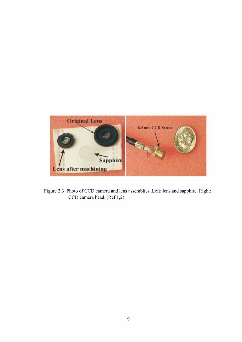
Figure 2.3 Photo of CCD camera and lens assemblies .Left: lens and sapphire. Right: CCD camera head. (Ref.1,2)
9

2.2 Example of optical design of reflectors
Usually, lighting devices use optical reflectors to greatly enhance the light
output on a target area. Such reflectors can be used to create a desired beam pattern
of the light intensity such that the output beam of the finished signal lamp will
efficiently meet the desired photometric specification. In many reflector designs, the
reflecting elements are typically metalized cavities with straight or parabolic edges.
An example of an optical reflector used to enhance the intensity from a LED lamp is
shown in Figure 2.4.3 The reflector cavities are used to enhance the outward beam
pattern.
Reflector cavities are used to redirect the light from the LED into a more
useful beam pattern. In most reflector design analysis, a LED or other small lamp can
be treated as a point source. This treatment is very accurate for large parabolic or
cone reflector geometries where the size of the LED is small relative to the exit
aperture of the reflector. As an example, a parabola shape is often used to collimate
the light beam emitted from a point light source and the point light source is placed at
the focal point of the parabolic reflector. As such, for a parabolic reflector design,
the focal length of the parabola is often related to the placement of the point light
source and the bottom of the reflector. The further the distance from the point source
to the bottom aperture of the reflector, the longer the focal length of the parabola
reflector. It should be noted that in order to produce a reflector with a cutoff angle
less than 20°, the height must increase radically. For this reason, reflectors with a high
degree of collimation (<20°) are often impractical. In addition, it can be seen that
10

Figure 2.4 Example of optical reflector used to enhance intensity from LED lamp
(Ref. 3)
11

reflectors with smaller focal lengths can produce a greater degree of collimation in a
shorter length. However, the exit aperture also becomes smaller. In order to get as
much light on the target, there is a tradeoff between the focal length and the degree of
collimation. 3,4
There are many other methods to design reflectors for LED sources. For
example, non-imaging techniques focus on extracting the light from the LED source
and redirecting the beam to have the desired divergence A rotationally symmetric
reflector technique developed by William B. Elmer, maps the flux into the desired
output beam. In his technique, he breaks the beam into angular sections, each
containing a known percentage of the total flux.4 It is then determined at what angle
each of these flux packets should be reflected to produce the desired output beam. The
profile of the final reflector will consist of a series of straight sections. As the number
of flux packets considered increased, the number of steps in the reflector increases,
until a smooth curve is approximated. Many of these design techniques are related to
commercial lighting using LEDs.
12

CHAPTER 3. EXPERIMENTAL MEASUREMENTS
This chapter presents our experimental measurements conducted to measure
the LED light intensity and preliminary reflector design measurements. Our
experimental setup is presented, and some of the features of the optical devices
including LED sources, photodiode , video camera and oscilloscope are characterized
and presented in this chapter.
3.1 Experimental Setup and Apparatus
In order to conduct preliminary experiments, we used LEDs, photodiodes, and
CCD cameras that were readily available in our lab; it is anticipated that these
experiments will be repeated after the optimized LEDs and HD CMOS or CCD
cameras are purchased and received. Our experiments were conducted to become
familiar with the LED intensity measurement techniques and to be able to compare
these results with some initial ray tracing predictions.
A schematic diagram of our LED light illumination experiment is shown in
Fig 3.1. The LED source was placed on an optical table, and a silicon photodiode
(UTD Sensors, Model PIN SC/10D) was placed at some distance (several centimeters)
above the LED. The output from the photodiode was fed into an oscilloscope. The
photons hitting the photodiode generated an electron current and transferred into a
13

voltage display on the oscilloscope. We moved the photodiode along the horizontal
direction from left to right and recorded the voltage for different viewing angles from
-90 to 90 degrees in steps of 10 degrees. We then plotted the voltage as a function of
the viewing angle to obtain the LED light distribution.
3.2 LED/photodiode parameters
For the LED light distribution measurement, a triple green LED (Model UT-
692NG ,L.C.LED Corp) was used , consisting of three small green LEDs, with each
LED having a dimension of 1.6mm x 0.8mm; 5 the three LEDs were placed next to
one another so that the overall size of the lighting area of the three LEDs was about
1.6 mm x 3 mm. A photograph of the three LEDs on a PC board is shown in Fig. 3.2.
Table 3.1 shows the data sheet of the LED that was used in the experiment. It
operated at a temperature of 25 C and had a viewing angle of 170 degrees.
The photodetector used was a Si photodiode (PIN SC/10D ,UDT Sensors Inc).
Figure 3.3 shows a photo of the detector, Fig. 3.4 gives the Si photodiode’s spectral
response, and Table 3.2 lists the typical specifications for this Si photodiode detector.
The dimension of the sensor area was about 10mm x 10mm, and the total sensing area
14

Figure 3.1 Schematic of LED light distribution experiment
15

Figure 3.2 Photograph of triple LED (green)
16

Table 3.1 Electro-optical properties of LED, Model UT-692NG Green Chip SMD LED( L.C.LED, Ref 5)
17
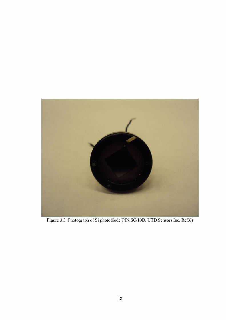
Figure 3.3 Photograph of Si photodiode(PIN,SC/10D. UTD Sensors Inc. Ref.6)
18

Figure 3.4 Spectral response of Si photodiode, Model PIN SC/10D ( UTD Sensors
Inc, Ref.6)
19

Table 3.2 Typical electro-optical specifications at T=23oC for Si photodiode. Model
PIN SC/10D (UTD Sensors Inc ,Ref 6 )
20

was 103 mm2 . This photodiode had one anode and four cathodes, but only one
cathode was used.6 Tests of the active area of the 1cm x 1cm detector indicated equal
sensitivity over the entire surface area. Note that the maximum recommended incident
power density is 10 mW / cm2. Typical uniformity of response for a 1 mm spot size
was given as ± 2%. The anode of the photodiode detector was directly connected to
the negative electrode of the oscilloscope, and the cathode of the photo detector was
connected to the positive electrode of the oscilloscope. We expect the photocurrent to
be linearly proportional to the illuminance. In the voltage measurement, an
oscilloscope ( Model 2235 100MHz, Tektronix .Inc) was used.
Several different metal reflectors were formed and placed about the LED
assembly in order to measure the enhanced light intensity due to the reflectors. For
ease of fabrication, several cones were manufactured from plastic substrates (by a
colleague of Pete Savage, Mr. Walter Kreiseder) and then aluminum foil was placed
manually into the surfaces of the cones. Figure 3.5 shows a photograph of the
aluminum foil lined cone reflectors. They had different cone angles, as seen, with
half angles of 10 , 20 , and 30 degrees.
Figure 3.6 shows a photograph of the cone placed over the LED; in this case
the 30 degree half angle cone reflector is shown. The height of each of the cones was
the same, 14.3mm, and the diameter of the cone was 25mm. The inside diameter of
the base of the cone was 5 mm; the inside diameter at the top of the cone was
approximately 8.8; 13.5mm; and 21mm for the 10, 20, and 30 degree cone,
21

respectively. The internal surface of the cones was covered with aluminum foil (with
the shinny side placed toward the LED light emission).
The aluminum coated reflectors were tested in our laboratory system. Figure
3.7 is a photograph of the laboratory system used to measure the angular dependence
Figure 3.5 Photograph of aluminium foil cone reflectors with different half angle,
from left to right: half angle of 10 o, 20 o, 30 o
22

Figure 3.6 Photograph of LED (green) with cone reflector made of aluminium foil
23

Oscilloscope DC Power supply
Photodiode LED/Cone reflector Figure 3.7 Photograph of the laboratory system used to measure angular dependence
of LED optical output.
24

of the LED optical output. .The electrodes of the power supply were connected to the
lead wires of the LED (voltage around 3.2V, current about 15mA); other colors of
LEDs were also available, such as white and blue, and will be tested at a later date for
possible color enhancement of the tissue images. In this experiment, the green triple
LED was tested. The voltage from the photodiode was measured on the oscilloscope
screen as the photdiode position was moved left to right. In this way, the angular
dependence of the LED optical output was measured with/without the reflector cones.
Figure 3.8 shows the LED light distribution measured with/without the cone
reflectors using the 1cm x 1cm Si photodetector; the distance between the LED and
photodetector was 2cm. To increase the spatial resolution, the photodetector was
reduced in active area using a mask to a size of 5mm x 5mm, and the distance from
the LED was increased to 5cm. Figure 3.9 shows their results. As can be seen, the
intensity falls off as the angle increases, and that smaller half- angle cones lead to
sharper light distribution patterns. The pattern without a cone is much flatter and
broader than that with the cones. In this case, it appears that the highest intensity was
seen for a 10 or 20 degree (half-angle) cone reflector.
Some preliminary experiments were conducted to study the amount of light
required to produce a good image using the LED sources and the trial CCD camera.
We conducted these experiments because initial results in the College of Engineering
indicated that there was not sufficient light to create a CCD image. We obtained a
similar camera, and tested it in our lab. The CMOS camera used was a QV7949 Color
CMOS (Omni Vision.Inc) camera and Table 3.3 gives its data sheet.7
25

Figure 3.8 Measured LED light distribution using different light reflecting cones;
distance was 2cm
26
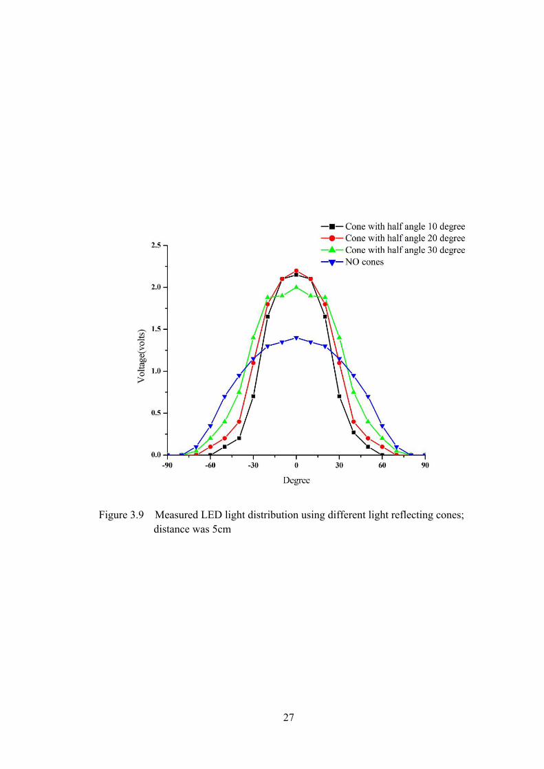
Figure 3.9 Measured LED light distribution using different light reflecting cones;
distance was 5cm
27

Table 3.3 QV7949 Color CMOS data sheet(Omni Vision.Inc. Ref. 7 )
28

Figure 3.10 presents our measurements of the resultant camera image using LED
(green) source with/without cones when the distance between the LED and the target
area was 10 cm; a sheet of yellow paper with a black drawing was used as the target.
In Fig. 3.10, the upper left image is the camera display without using a reflector, the
upper right is with a 10 degree cone reflector, the lower left is with a 20 degree cone,
and the lower right is with a 30 degree cone. The four images clearly show how the
light brightness on the CMOS camera improves using the cone reflectors. It’s a little
difficult to tell the difference between each angle of cone reflector due to the color of
the background and the possible automatic gain control of the CMOS camera chip.
Figure 3.10 CCD Camera images of drawing on paper target. Upper left: without reflector. Upper right:10o half angle cone. Lower left: 20o half angle cone. Lower right: 30o half angle cone
29

CHAPTER 4. INITIAL SIMULATIONS USING TRACEPRO RAY TRACING
SOFTWARE
In this chapter, initial simulations using the TracePro ray tracing software are
presented and the simulation result are compared and correlated with some initial
experiment result.
4.1 TracePro Software
TracePro is a commercial optical engineering software developed by Lambda
Research Corporation for scientists and engineers to design and analyze optical and
illumination systems.8 It is a comprehensive, versatile software tool for modeling the
propagation of light in imaging and non-imaging opto-mechanical systems. Models
are created by importing from a lens design program, a Computer Aided Drafting
(CAD) program, or by directly creating the solid geometry in TracePro. Optical
properties are assigned to materials and surfaces in the model. Optical source rays
propagate through the model with portions of the flux of each ray allocated for
absorption, specular reflection and transmission, fluorescence, and scatter. From the
model, ray tracing can analyze light distributions in illumination and imaging systems
and loss and system transmittance, amongst a host of other optical considerations
(polarization, birefringence, etc.). Ray tracing is the means by which TracePro
simulates the distribution of optical flux throughout a model or at selected surfaces.
30

TracePro provides a comprehensive set of tools to view and analyze the results of the
ray trace, including irradiance and illuminance maps. After a Luminance Map is ray
traced, it may be displayed as true color or a photorealistic rendering based on the
wavelengths traced. The results of the ray trace may be displayed as either a
Luminance or Radiance Map with photometric units (cd/m2, foot-lambert, or
millilamber) or radiometric units (W/m2) respectively.8
We were able to obtain a copy of TracePro with a 30 Day Trial period for
college students. Here, the author is greatly thankful to the Lambda Research
Corporation who extended my TracePro 30 day trial period to a half year.
As an example of the capability of the TracePro program, Figure 4.1 shows
the interface page and plot for the design of an elliptical lamp design.9 A more
specific example showing the ray tracing capability is shown in Figure 4.2, which is
an example of ray tracing for the emission from a LED using a collimating half-
spherical lens.10
31

Figure 4.1 Elliptical lamp design using TracePro software (Ref.9)
32

Figure 4.2 Blue LED excitation and yellow luminescence rays propagating through
3-D solid model in TracePro(Ref.10)
33

4.2 Initial simulations using TracePro
An initial point model of the light output from a LED was modeled. Figure
4.3 shows the geometry of the LED light distribution experimental model we used in
the TracePro software. Here, the LED and aluminum cone reflectors are shown. In
addition, the upper large disk is the geometrical area through which the TracePro
program calculates the ray tracings. For consistency, the LED emission flux was
about 1 Watt, the angular distribution was Lambertian, wavelength of 500nm, and
about 4000 rays were emitted in total. The cone reflector had a 100% reflectivity on
the cavity surface. A disc calculation target area (the upper large disk in Fig. 4.3) had
a radius of 20mm and was set 20mm away from the LED base. That distance
corresponds to a +/- 45 degree viewing angle. The cone reflectors had the same
parameters as those used in our experiments and included cones with a half angle of
10 , 20 , and 30 degrees. The length of the cones was the same, 14.3mm, and all the
base diameter of the reflecting cones was the same 5mm. As can be seen from Fig
4.3, most of the rays hit the calculation target area.
The resultant calculations were made and the relative flux density of the ray
tracings (or light intensity) was plotted as a function of the angle from the LED
surface normal. Figure 4.4 shows the LED light distribution predicted using the
TracePro software. These results indicate that the 10 and 20 degree angle cone
reflectors produced significant increases in the light intensity. Of importance is that
they also are consistent with our preliminary experiments of the LED light
distribution shown in Fig 3.8. These results are important because they give one
34

confidence that other related optical design calculations using the TracePro program
are probably good estimates of real measurements.
Figure 4.3 Geometry of LED light distribution experimental model in TracePro software. The LED and Al cone reflector are shown. The upper large disk is the geometrical area through which the TracePro program calculates the ray tracing.
35

Figure 4.4 Predicted LED light distribution using TracePro software when LED distance is 2 cm
36

Figure 4.5 Predicted LED light distribution using TracePro software when LED
distance is 5 cm
37
CHAPTER 5. PREDICTED INTENSITY ANGULAR DISTRIBUTION OF
DIFFERENT OPTICAL DESIGNS USING RAY TRACING PROGRAM
This chapter presents the simulation results and optimization of different
optical designs using the Trace-Pro software. These simulations are important because
they demonstrate the relation between optical geometries and light illumination.
Further, they give the optimal optical design for the best LED light output and images
received at the CCD sensors.
5.1 Initial geometry of LED, half-sphere holders, and parabola reflectors
The geometry for the LEDs illumination consideration can be seen in Figure
5.1. Here, Fig. 5.1 shows a cross-section view of the LED contained within a half-
sphere base. The size of each individual LED is about 1.5mm x 1.5mm x 0.2mm,
with the half-sphere having a anticipated radius r of about 1.5mm. Figure 5.2
represents the cross-section view of the LED base with the addition of a parabolic
reflector. Here, the bottom of the half-sphere spherical surface is about 0.6mm below
that of the LED. In addition, the focal point of the parabola is along the z axis, and is
shown for several values above the position of the LED.
38

Figure 5.1 Design of LED base within spherical well. LED size is 1.5mm x 1.5mm x
0.2mm with the half-sphere radius r=1.5mm..
39

Figure 5.2 Cross-section view of LED base for parabolic reflector
40
5.2 Different optical reflector geometries
Different optical reflector geometries were studied in order to enhance the
LED light intensity on a projected target area. Figure 5.3 is the CAD drawing of
three reflector geometries that were considered. They were a cone reflector, a
parabolic reflector, and a ‘collar’ reflector.
In order to test these three designs, we chose to use four LED sources in a ring
geometry, as a way to increase the number of illuminating areas; we also looked at a
design using 9 LED sources, but plan to conduct these tests at a later time. As a
result, the reflector design used 4 LEDs in a circular array.
Each LED source was placed inside a spherical well on the PCB chip holder.
The half-spherical well’s surface was defined as a “default mirror.” The top surface
of the LEDs was assumed to be a Lambertian emitter, with spectra based on a
Luxeon I White model in the TracePro catalog.8 Other dimensions were: 10 mm
outer diameter, 4 mm inner diameter, 1.5 mm spherical well radius.
The resultant TracePro predictions were made, and a simplified plot is shown
in Fig 5.4 for illustrative purposes. Here, the LED ring with individual reflectors is
shown, but only 40 rays are emitted and traced. In the actual calculations, 4000 rays
were emitted and traced. As indicated, three proposed reflector designs were studied:
a cone reflector, a parabolic reflector, and a collar reflector. The former two designs
involved fitting individual reflectors over each LED, while the collar design would fit
a big trough reflector (with flat sides) around all of the LEDs. The cone reflectors had
41
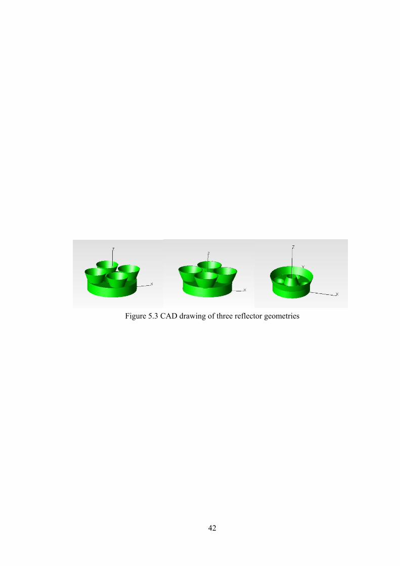
Figure 5.3 CAD drawing of three reflector geometries
42

Figure 5.4 LED ring with individual reflectors showing predicted optical ray tracing
43

a straight wall surface, while the parabolic reflectors had a parabolic wall surface.
The collar reflector also had straight walls.
For the analysis, a target area (ie. TracePro limited calculation area) with a
radius of 50 mm was placed at a distance of 5 cm from the LED base, corresponding
to a maximum +/- 45° half-angle spread about the normal. All the cone and collar
reflectors had the same heights of 2mm, while some parabolic reflectors had heights
of less than 2 mm. In the simulations, a target detector area of 1 cm2 was used to
calculate the flux density or number of rays passing through the 1 cm2 detector area.
Then the detector area was moved left and right (ie. +/- 5 cm) across the calculation
area. It was then possible to count the number of rays that passed through this target
detector area and determine the relative light intensity as a function of angle for a
given reflector design.
As a first approximation as to the utility of the reflectors, we calculated the
total fraction of rays that were emitted from the LEDs and that were emitted outward
within the +/- 45 degree "Calculation Limit Area" shown in Fig. 4.3. Our results are
shown in Figure 5.5 which plots the fraction of the rays that hit the calculation limit
area for the cone and collar geometries as a function of half-angle for the cone and
collar reflectors. Also shown are the results for the LED when no reflector was used;
here, the fraction of rays emitted through the +/- 45 degree calculation limit area was
64.13%. For the cone reflector, the fraction of emitted rays was almost a constant
value at 93%, while it was about 80% for the collar reflector. As can be seen, there
44

Figure 5.5 Fraction of the emitted rays that hit the +/- 45o Calculation Limit Area as a function of the half angle of reflector
45

was little difference for different half-angle values for the cone and collar reflector
angles.
Another study led to the calculation of the number of rays that were emitted
through the calculation area as a function of the focal length of the parabolic reflector.
These results are shown in Figure 5.6. The maximum through-put occurred when
the focal length of the parabolic reflectors was 0.4 mm, such that 95.8% of the
emitted rays hit the calculation area; here, the z = 0 position was defined to be the
bottom of the PCB chip.
In a similar calculation, Fig 5.7 presents the fraction of rays that hit the
calculation area as a function of the z position of the LEDs for the case where the
half-angle was about 20 degrees for the cone reflector. As can be seen, there was
almost no change in the fraction of rays hitting the area when the z position was
changed. The fraction was roughly 94% for z from 0.8mm to 1.8mm, with a slight
optimal z position of 1.4 mm corresponding to 97.53%.
Our resultant simulations of the expected flux intensity as a function of angle
from the normal is shown in Figures 5.8, 5.9, and 5.10 for the case of the cone
reflector, parabolic reflector, and collar reflector, respectively. Here, the number of
rays passing through a 1 cm2 detector area was calculated, the detector was 5 cm away
from the LED base, and the detector area was moved left to right along a horizontal
path above the LED. As can be seen from the plotted data, the optimized parabolic
reflector had the highest flux intensity at the center of the calculated area. However,
other focal lengths of the parabola significantly reduced the maximum intensities.
46

Figure 5.6 Fraction of the emitted rays that hit the +/- 45o Calculation Limit Area as
function of the focal length.
47

Figure 5.7 Fraction of rays that hit the +/- 45o Calculation Limit Area as a function of z position of LEDs within the half-spherical wells of the 20o cone reflector design.
48

Figure 5.8 Cone reflector intensity distribution simulation. Number of rays for 1 cm2 on 5cm away +/- 45o Calculation Limit Area as function of half-angle of cone reflector. 20o is the optimal half angle.
49

Figure 5.9 Parabolic reflector intensity distribution simulation. Number of rays for
1cm2 on 5cm away +/- 45o Calculation Limit Area as function of focal length of parabolic reflector. 0.4mm is the optimal length.
50

Figure 5.10 Collar reflector intensity distribution simulation. Number of rays for
1cm2 on 5cm away +/- 45o Calculation Limit Area as function of half-angle of collar reflector. 20o is the optimal half angle.
51

52
The cone reflectors showed almost as high of a maximum intensity, but offered a
more robust design in that changes in the cone angle were not as important in the
optimized values. Lastly, the collar approach was less intense than that of the cone
reflectors, but had values close to that of the non-optimized parabola reflector.

CHAPTER 6 PREDICTED INTENSITY SPATIAL PROFILES USING
TRACEPRO
The spatial intensity pattern was also studied using the TracePro program. The
predicted light intensity profiles were calculated for several geometries. The predicted
intensity profiles were calculated for each reflector geometry: no reflector, cone reflector,
parabolic reflector, and collar reflector. The distance from the LED source to the detector
area was set at 0cm, 2cm, and 5cm in order to estimate the relative light intensity for each
case. Finally, the intensity patterns were plotted for the above cases using (1) an
absolute intensity scale so that a comparison between each reflector could be made, and
(2) a relative or comparative intensity scale so that one can see the spatial profile even if
the intensity pattern is very weak.
Figures 6.1 to 6.8 show the absolute light flux intensity and relative/comparative
light intensity patterns of no reflector, cone reflector , parabolic reflector and collar
reflector geometries, all measured at a distance of 0 cm, 2 cm , and 5 cm from the LED
source. In the graphs of absolute light flux intensity patterns, the x and y axis has the
53

Figure 6.1 LED light pattern simulation (no reflector; absolute intensity), measured at
distance of 0 cm, 2 cm, and 5 cm from the LED Source (top to bottom). Max intensity axis value for each is 220,000 W/m2. The X and Y Axis represent dimension of +/- 5cm, each.
54

Figure 6.2 LED light pattern simulation (no reflector; relative intensity), measured at
distance of 0 cm, 2 cm, and 5 cm from the LED Source. Max intensity axis value is 220000, 9000, and 2200 W/m2, respectively (top to bottom). Here, X and Y axis is reduced to better show the beam intensity.
55
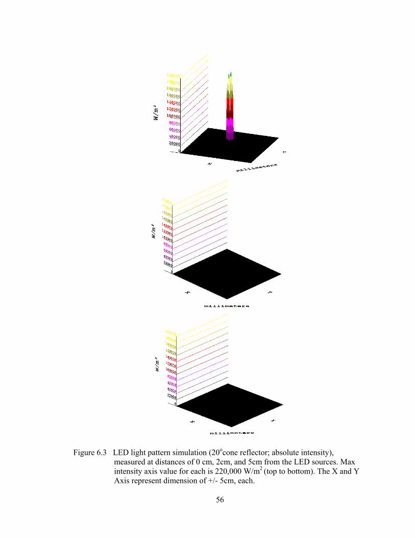
Figure 6.3 LED light pattern simulation (20ocone reflector; absolute intensity),
measured at distances of 0 cm, 2cm, and 5cm from the LED sources. Max intensity axis value for each is 220,000 W/m2 (top to bottom). The X and Y Axis represent dimension of +/- 5cm, each.
56

Figure 6.4 LED light pattern simulation (20o cone reflector; relative intensity), measured
at distances of 0 cm, 2cm, and 5cm from the LED sources. Max intensity axis value is 220000, 20000, and 6000 W/m2, respectively (top to bottom). Here, X and Y axis is reduced to better show the beam intensity.
57

Figure 6.5 LED light pattern simulation (f=0.4mm parabolic reflector; absolute intensity), measured at distances of 0 cm, 2cm ,and 5 cm from the LED sources ( top to bottom). Max intensity axis value for each is 220,000 W/m2. The X and Y Axis represent dimension of +/- 5cm, each.
58

Figure 6.6 LED light pattern simulation (f=0.4mm parabolic reflector; relative Intensity), measured at distances of 0 cm, 2cm ,and 5 cm from the LED
sources (top to bottom). Max intensity axis value is 220000, 19000, and 6500 W/m2, respectively. Here, X and Y axis is reduced to better show the beam intensity.
59

Figure 6.7 LED light pattern simulation (17.5o collar reflector; absolute intensity),
measured at distance of 0 cm, 2 cm, and 5 cm from the LED sources (top to bottom). Max intensity axis value for each is 220,000 W/m2. The X and Y Axis represent dimension of +/- 5cm, each.
60

Figure 6.8 LED light pattern simulation (17.5o collar reflector; relative intensity),
measured at distance of 0 cm, 2 cm, and 5 cm from the LED sources (top to bottom). Max intensity axis value is 220000, 13000, and 3800 W/m2, respectively. Here, X and Y axis is reduced to better show the beam intensity.
61

same spatial extent of +/- 50 mm, while the flux intensity has the same maximum scale
value of 2.2 x 10⁶ W/m2. For the relative/comparative light flux intensity plots, the
flux intensity scales differ for each plot and typically have much lower values especially
for the further distances.
Some overall observations can be made from the data. Figure 6.1 shows the
absolute LED light pattern simulation with no reflector and shows that the light flux
intensity decreases rapidly as the distance from the LED is increased. The flux intensity
pattern is almost the same for 2cm and 5 cm. Figure 6.2 shows the relative LED light
pattern simulation with no reflector, measured at a distance of 0 cm, 2 cm , and 5 cm
from the LED source. The light intensity shapes become broader as a function of distance.
The results also show that the average flux intensity at 2cm is 455.81 W/m2 and is 50%
more than that at 5cm.
Figure 6.3 shows the absolute LED light pattern simulation of 20 degree cone
reflector. The absolute light intensity for 2 cm is almost the same with 5cm. But from
Fig 6.4 , it is seen that the maximum flux intensity is larger at a distance of 2 cm. The
results show that the average flux intensity on the detector target when the distance is
2cm is 481.02W/m2 and 4% bigger than that at 5cm.
Figure 6.5 shows the absolute LED light pattern simulation of a f=0.4mm
parabolic reflector. The absolute light intensity has similar patterns with that of the cone
reflector. Figure 6.6 shows the relative LED light pattern simulation; the average flux
intensity on target for a distance of 2cm was 482.03W/m2 , and 2.8% more than that at
5cm.
62

Figure 6.7 shows the absolute LED light pattern simulation for a 17.5 degree
collar reflector. The absolute light intensity had a similar pattern to that of the cone and
parabolic reflector. Figure 6.8 shows the relative LED light pattern simulation; the
average flux intensity when d=2cm was 479.21W/m2 and 20% bigger than that at 5cm.
For comparison, Table 6.1 shows the peak intensity of each of these reflector
geometries at the different distances. As can be seen, the parabolic and cone reflector
geometries yield similar peak intensities.
Table 6.1 Maximum intensity value for different reflectors at different distances
63

CHAPTER 7. INITIAL OPTICAL DESIGN FOR CCD CAMERA AND LENS
ASSEMBLY
It was proposed early on that a CCD (or CMOS) video camera could be used for
forming the image of the illuminated target area, and that a lens would be used to help
form the image on the camera CCD/CMOS chip surface. The design of the lens and
camera system is driven by the trade-off between image size, target area distance away
from the camera, and the desired Field-of-View (FOV) of the system. Some constraints
are that it was desired to keep the lens thin (less than 2mm thick). The geometry of the
system can be depicted in Fig 7.1 which shows a schematic diagram of a camera, which
is similar to that of a lens and CCD system. Here, the CCD has a width or size of d, the
target area (object) is a distance S1 from the lens, the CCD surface (image plane) is a
distance S2 from the lens, and f is the focal length of the lens. The CCD viewing angle
can be given as
tan(α/2) = d/2f , (7.1)
where α is the CCD viewing angle, d is the diameter of the CCD, and f is the focal length
of the lens (Note: in Fig.7.1, F is indicated as the focal length). 11
64

Figure 7.1 Schematic diagram of Lens and CCD system (Ref.12)
65

For a specific example, the probe designers in the College of Engineering
proposed using a High-Definition camera, a CMOS (Model OV 6930, Omni Vision)
which has a detector size of 1.224mm x 1.224mm.13 The data sheet of the CMOS is
given in Figure 7.2. Using the dimension of the CMOS chip (d=1.22mm) and assuming
that the desired camera viewing angle is about 60 degrees, the focal length of the lens can
be calculated using Eq. (7.1) to be about f = 1.22mm/(2 tan30) = 1.05mm. The F-
number, F#, of the lens is defined as F# = f/D, where D is the diameter of the lens. In
order to provide for low-light imaging, the F- number was selected to be 4; a lower
number would be better in order to capture more light, but is harder to manufacture
without introducing optical aberrations in the image.2 As such, the diameter of the lens
can be estimated as
D = f/F# = 1.05mm/4 = 0.26mm. (7.2)
In summary, for this example, the lens would have a focal length, f, of 1.05 mm, and a
diameter, D, of 0.26mm, and the CMOS/CCD chip size is about 1.22mm. Figure 7.3
shows some typical lens manufactured that are close to the desired parameters.14
Further considerations can be made using the lens equation15 given by
1/f = 1/S1 + 1/S2 . (7.3)
The magnification, m, is given by m = - S2 / S1. For the case of the object distance of
50mm, and f of 1.05 mm, Eq. (7.3) yields an image distance, S2, of about 1.072mm.
The magnification, m, of the object to form the image is thus about 0.0214. This
indicates that the object size at the target area is equal to the CCD size, d, divided by the
magnification, m , or d/m = 1.22 mm / .0214 = 57 mm. As such, the size of the target
66

area imaged by the CCD is about 57 mm across at a distance of 50 mm away. This
represents a viewing angle of about +/- 29 degrees.
Figure 7.2 Datasheet of CMOS (Model OV 6930, Omni Vision. Ref.13)
67

Figure 7.3 Parameters of the desired lens configuration (Universe Kogaku America Inc. Ref.14)
68

The above example serves to point out the design method to help optimize the
CCD and lens system. The illumination beam size of the LED/rerflector combination
also has to be considered. It is expected that trade-offs will have to be made between
image brightness and field of view in the TV image.
Finally, it should be mentioned that we use the term CCD and CMOS almost
interchangeably in this thesis. This is because both are imaging camera chips that have
some technical differences but both can be used for High-Definition imaging. Some of
the differences are as follows: CCD (charge coupled device) and CMOS (complementary
metal oxide semiconductor) image sensors are two different technologies for capturing
images digitally. Each has unique strengths and weaknesses giving advantages in
different applications. Both CCDs and CMOS imagers can offer excellent imaging
performance when designed properly. CCDs have traditionally provided the performance
benchmarks in the photographic, scientific, and industrial applications that demand the
highest image quality (as measured in quantum efficiency and noise) at the expense of
system size. CMOS imagers offer more integration (more functions on the chip), lower
power dissipation (at the chip level), and the possibility of smaller system size, but they
have often required tradeoffs between image quality and device cost. Today there is no
clear line dividing the types of applications each can serve. CMOS designers have
devoted intense effort to achieving high image quality, while CCD designers have
lowered their power requirements and pixel sizes. As a result, you can find CCDs in low-
cost low-power cellphone cameras and CMOS sensors in high-performance professional
and industrial cameras, directly contradicting the early stereotypes.16
69

CHAPTER 8. CONCLUSION AND FUTURE WORK
The optical design of a LED illumination system and a imaging camera was
investigated for the purpose of placing a small light/TV camera inside the human body to
help minimally invasive surgery. Some experiments were conducted to measure the
light distribution using a LED source and different reflector concentrators. Ray tracing
simulations were conducted and the results were in good agreement with the experiments.
The TracePro ray tracing simulations were expanded to include a larger variety of
reflector geometries including cone reflectors, parabolic reflectors, and a collar reflector.
These results indicated that a reflector geometry that concentrated the light into a beam
width of about +/- 20 degrees was close to optimal.
Considerations of the CCD camera and imaging lens was studied. These results
indicated that a micro-lens could be used with the CCD to image the tissue target onto the
CCD camera using the LED as the illumination source.
Further work is required to better optimize our results, and to perform
experimental lab measurements that can duplicate our reflector geometry simulations and
CMOS/CCD camera/lens calculations.
70

REFERENCES
1. Tie Hu, Peter K. Allen, “Insertable Stereoscopic 3D Surgical Imaging Device with Pan and Tilt”,Proceedings of the 2nd Biennial IEEE/RAS-EMBS International
Conference on Biomedical Robotics and Biomechatronics (2008). 2. Tie Hu, Peter K. Allen, Nancy J. Hogle and Dennis L. Fowler,“Insertable Surgical
Imaging Device with Pan, Tilt, Zoom, and Lighting”, The International Journal of Robotics Research 28; 1373 (2009).
3. “Secondary Optics Design Considerations for SuperFlux LEDs”, Publication No.
AB20-5,Lumileds Lighting LLC (2002) 4. William B. Elmer. “The Optical Design of Reflectors”, Second Edition, John Wiley&
Sons, Inc. (1980) 5. UT-692NG LED’s Datasheet (L.C.LED Corporation) (2000) 6. Tetra-lateral psd's Position Sensing Detectors’ datasheet, UTD Sensors ,Inc 7. QV7949 Color CMOS Manual Version 2.6 ,Omni Vision.Inc (2009) 8. “TracePro Manual Revision 03” , Lambda Research Corporation(2009) 9. TracePro, Lambda Research Corporation(2010) 10. “Improved predictive modeling of white LEDs with accurate luminescence simulation and practical inputs” Technical note, Lambda Research Corporation(2010) 11. “UNDERSTANDING & USING CCD CAMERAS” Electus Distribution, 2001 12. www.wikipedia.com; Angle of view/camera 13. Datasheet of CCD, Model OV 6930, Omni Vision Technologies. Inc (2009) 14. “CCD Lens Assemblies”, Universe Kogaku America Inc(2010) 15. Serway Jewett “Physics for Scientists and Engineers” 6th Edition (2004) 16. www.Dalsa.com website
71

APPENDICES
72

APPENDIX A. Early Poster Presentation at REU/USF Summer Conference
This appendix shows a copy of the earlier presented poster presentation which
showed initial simulation studies conducted by REU summer student Susanna Todaro
and Weiyi He
Figure A.1 Early Poster Presentation at REU/USF Summer Conference
73