Embed Size (px)
Citation preview

OPERATION OF THE AERODYNAMIC PLASMA ACTUATOR AT HIGH
ALTITUDE
by
TIMOTHY GLEN NICHOLS
A THESIS
Presented to the Faculty of the Graduate School of the
MISSOURI UNIVERSITY OF SCIENCE AND TECHNOLOGY
In Partial Fulfillment of the Requirements for the Degree
MASTER OF SCIENCE IN AEROSPACE ENGINEERING
2012
Approved by
Joshua L. Rovey, Advisor
Serhat Hosder
Fathi Finaish

2012
Timothy Glen Nichols
All Rights Reserved

iii
ABSTRACT
A plasma actuator was operated at altitudes from 0 to 18288 meters to determine
the mechanisms leading to decreased force production at low pressures. The actuator was
driven with a 5 kHz sine wave and a peak to peak voltage of 13.4 kV at pressures of 760,
429, 321, 226, and 88 Torr. A passive measurement technique called the capacitive V-dot
probe was adapted to the actuator in order to resolve the spatiotemporal evolution of the
surface potential and electric field on the dielectric surface. At low pressures up to 20
times more plasma is present than at atmospheric conditions. Average force production is
calculated and shown to decrease at lower pressures due to the fact that up to 88% of the
plasma is created in regions where the electric field is approximately zero. The calculated
average body force shows a slight increase up to a pressure of 429 Torr before trending to
zero at lower pressures. Performing a power analysis shows that as pressure is decreased
more power is used creating plasma than accelerating it, leading to a decrease in
efficiency.

iv
ACKNOWLEDGMENTS
I would first like to thank my advisor, Dr. Joshua Rovey, for all of his help and
guidance throughout my years at S&T. Without his understanding and encouragement I
would not have completed this thesis. I would also like to think Dr. Serhat Hosder and
Dr. Fathi Finaish for serving as my committee members as their advice and help with this
project have been greatly appreciated.
I would also like to thank all of the students in the Aerospace Plasma Lab: Jing,
Steve, Ryan, Alex, Mark, Andrew, and Warner. The help I received with my project from
everyone was fantastic and helped me more than some of you may know. Also, the
conversations we have had (academic and non-academic alike) have been a great pleasure
of mine since joining the lab.
Finally, I’d like to thank my family (Tina, Sam, and Jonathan Nichols) and my
girlfriend, Meagan Kreps. Though you probably understood little to nothing of my
research when I spoke of it, serving as a frustration vent was more help than even I
realized until now. Even more, you believed in me to accomplish my goals and to live out
a dream and for that I will be forever thankful.
v
TABLE OF CONTENTS
Page
ABSTRACT ....................................................................................................................... iii
ACKNOWLEDGMENTS ................................................................................................. iv
LIST OF ILLUSTRATIONS ............................................................................................ vii
NOMENCLATURE .......................................................................................................... xi
SECTION
1. INTRODUCTION ...................................................................................................... 1
1.1. DBD ACTUATOR INTRODUCTION .............................................................. 1
1.2. DBD ACTUATOR OPERATION ...................................................................... 2
1.3. PREVIOUS RESEARCH ON DBD ACTUATORS AT HIGH ALTITUDE .... 3
2. EXPERIMENTAL TECHNIQUES AND SETUP .................................................... 5
2.1. BASIC PLASMA ACTUATOR OPERATION ................................................. 5
2.2. ANALYSIS OF A CAPACITIVE V-DOT PROBE ........................................... 7
2.2.1. Charging of the Bulk Capacitance – 1st Calibration. ................................ 8
2.2.2. Surface Charging – 2nd
Calibration ........................................................ 11
2.2.3. Charge Due to Capacitive Voltage Division and Polarization of
Dielectric Material. ................................................................................ 12
2.3. PLASMA ACTUATOR.................................................................................... 13
2.4. V-DOT PROBE ELECTRONICS .................................................................... 15
2.5. HIGH ALTITUDE TESTING SETUP ............................................................. 15
3. RESULTS ................................................................................................................. 17
3.1. PLASMA EXTENSION AND POWER CONSUMPTION ............................ 17
3.2. SURFACE POTENTIAL AND ELECTRIC FIELD MEASUREMENTS ...... 20
3.3. AVERAGE SURFACE POTENTIAL AND CHARGE TRANSFERRED ..... 55
3.4. ION DENSITY ................................................................................................. 56
4. DISCUSSION .......................................................................................................... 64
4.1. SURFACE POTENTIAL AND CHARGE BUILD-UP ................................... 64
4.2. LOCATION OF PLASMA PRODUCTION .................................................... 64
4.3. QUALITATIVE FORCE TRENDS ................................................................. 66

vi
5. CONCLUSION ........................................................................................................ 69
APPENDICES
A. MISCELLANEOUS PLOTS ................................................................................. 70
B. DETAILED TROUBLESHOOTING OF EXPERIMENTAL SETUP ................. 83
BIBLIOGRAPHY ............................................................................................................. 84
VITA. ................................................................................................................................ 93

vii
LIST OF ILLUSTRATIONS
Page
Figure 1.1: Schematic diagram of a DBD plasma actuator.. .............................................. 2
Figure 2.1: The spacing of the V-dot probes is such that at low pressures the charge on
the dielectric surface can be measured over the entire extent of the plasma,
not just close to the exposed electrode. ........................................................... 7
Figure 2.2: Each buried segmented electrode is connected to an op-amp based integrator
circuit with a large resistor in parallel (50 MΩ in this experiment) with the
integrating capacitor, Cint................................................................................. 7
Figure 2.3: Lumped circuit model of the DBD plasma actuator
(from Enloe et al. [1]). ................................................................................... 10
Figure 2.4: The response of the V-dot probe to the charging of the “bulk capacitance”
is linear. ......................................................................................................... 10
Figure 2.5: The 1st calibration factor ranges from K1 = 0.348 V/kV at the closest probe
to 0.007 V/kV at the farthest probe. .............................................................. 11
Figure 2.6: The large Macor dielectric provides enough surface area to prevent arcing
at low pressures. ............................................................................................ 14
Figure 2.7: A 5 kHz sine wave is generated with the function generator and then
stepped up through an amplifier and step-up transformer to kV levels. ....... 14
Figure 2.8: 1. Vacuum Chamber; 2. BNC-BNC Passthrough; 3. Lesker Pressure Gauge;
4. Tektronix DPO 2024 Oscilliscope; 5. Op-Amp Integrator Circuit;
6. Rigol Function Generator; 7. Faraday Cage; 8. Crown Amplifier ............ 16
Figure 3.1: Applied waveform (black) and corresponding current plot (red) with four
distinct time intervals labeled. ....................................................................... 18
Figure 3.2: Decreasing the pressure increases power consumption and also causes
plasma to form farther downstream. .............................................................. 18
Figure 3.3: Pictures taken with 1/3s exposure time show the time averaged plasma
distribution on the dielectric surface. ............................................................ 19
Figure 3.4: 3D plot of surface potential as a function of downstream position and time
at 760 Torr. .................................................................................................... 21

viii
Figure 3.5: 3D plot of surface potential as a function of downstream position and time
at 429 Torr. .................................................................................................... 21
Figure 3.6: 3D plot of surface potential as a function of downstream position and time
at 321 Torr. .................................................................................................... 22
Figure 3.7: 3D plot of surface potential as a function of downstream position and time
at 226 Torr. .................................................................................................... 22
Figure 3.8: 3D plot of surface potential as a function of downstream position and time
at 171 Torr. .................................................................................................... 23
Figure 3.9: 3D plot of surface potential as a function of downstream position and time
at 88 Torr. ...................................................................................................... 23
Figure 3.10: Potential on the surface of the dielectric between t1 and t2 at 760 Torr. ....... 28
Figure 3.11: Electric field near the dielectric surface between t1 and t2 at 760 Torr. ....... 28
Figure 3.12: Potential on the surface of the dielectric between t2 and t3 at 760 Torr. ....... 29
Figure 3.13: Electric field near the dielectric surface between t2 and t3 at 760 Torr. ....... 29
Figure 3.14: Potential on the surface of the dielectric between t3 and t4 at 760 Torr. ....... 30
Figure 3.15: Electric field near the dielectric surface between t3 and t4 at 760 Torr. ....... 30
Figure 3.16: Potential on the surface of the dielectric after t4 at 760 Torr. ....................... 31
Figure 3.17: Electric field near the dielectric surface after t4 at 760 Torr. ........................ 31
Figure 3.18: Potential on the surface of the dielectric between t1 and t2 at 429 Torr. ....... 32
Figure 3.19: Electric field near the dielectric surface between t1 and t2 at 429 Torr. ....... 32
Figure 3.20: Potential on the surface of the dielectric between t2 and t3 at 429 Torr. ...... 33
Figure 3.21: Electric field near the dielectric surface between t2 and t3 at 429 Torr. ....... 33
Figure 3.22: Potential on the surface of the dielectric between t3 and t4 at 429 Torr. ...... 34
Figure 3.23: Electric field near the dielectric surface between t3 and t4 at 429 Torr. ....... 34
Figure 3.24: Potential on the surface of the dielectric after t4 at 429 Torr. ...................... 35
Figure 3.25: Electric field near the dielectric surface after t4 at 429Torr. ........................ 35
Figure 3.26: Potential on the surface of the dielectric between t1 and t2 at 321 Torr. ....... 36
Figure 3.27: Electric field near the dielectric surface between t1 and t2 at 321 Torr. ....... 36
Figure 3.28: Potential on the surface of the dielectric between t2 and t3 at 321 Torr. ...... 37
Figure 3.29: Electric field near the dielectric surface between t2 and t3 at 321 Torr. ....... 37
Figure 3.30: Potential on the surface of the dielectric between t3 and t4 at 321 Torr. ...... 38

ix
Figure 3.31: Electric field near the dielectric surface between t3 and t4 at 321 Torr. ....... 38
Figure 3.32: Potential on the surface of the dielectric after t4 at 321 Torr. ...................... 39
Figure 3.33: Electric field near the dielectric surface after t4 at 321 Torr. ....................... 39
Figure 3.34: Potential on the surface of the dielectric between t1 and t2 at 226 Torr. ....... 43
Figure 3.35: Electric field near the dielectric surface between t1 and t2 at 226 Torr. ....... 43
Figure 3.36: Potential on the surface of the dielectric between t2 and t3 at 226 Torr. ...... 44
Figure 3.37: Electric field near the dielectric surface between t2 and t3 at 226 Torr. ....... 44
Figure 3.38: Potential on the surface of the dielectric between t3 and t4 at 226 Torr. ...... 45
Figure 3.39: Electric field near the dielectric surface between t3 and t4 at 226 Torr. ....... 45
Figure 3.40: Potential on the surface of the dielectric after t4 at 226 Torr. ...................... 46
Figure 3.41: Electric field near the dielectric surface after t4 at 226 Torr. ....................... 46
Figure 3.42: Potential on the surface of the dielectric between t1 and t2 at 171 Torr. ....... 47
Figure 3.43: Electric field near the dielectric surface between t1 and t2 at 171 Torr. ....... 47
Figure 3.44: Potential on the surface of the dielectric between t2 and t3 at 171 Torr. ...... 48
Figure 3.45: Electric field near the dielectric surface between t2 and t3 at 171 Torr. ....... 48
Figure 3.46: Potential on the surface of the dielectric between t3 and t4 at 171 Torr. ...... 49
Figure 3.47: Electric field near the dielectric surface between t3 and t4 at 171 Torr. ....... 49
Figure 3.48: Potential on the surface of the dielectric after t4 at 171 Torr. ...................... 50
Figure 3.49: Electric field near the dielectric surface after t4 at 171 Torr. ....................... 50
Figure 3.50: Potential on the surface of the dielectric between t1 and t2 at 88 Torr. ......... 51
Figure 3.51: Electric field near the dielectric surface between t1 and t2 at 88 Torr. ......... 51
Figure 3.52: Potential on the surface of the dielectric between t2 and t3 at 88 Torr. ........ 52
Figure 3.53: Electric field near the dielectric surface between t2 and t3 at 88 Torr. ......... 52
Figure 3.54: Potential on the surface of the dielectric between t3 and t4 at 88 Torr. ........ 53
Figure 3.55: Electric field near the dielectric surface between t3 and t4 at 88 Torr. ......... 53
Figure 3.56: Potential on the surface of the dielectric after t4 at 88 Torr. ........................ 54
Figure 3.57: Electric field near the dielectric surface after t4 at 88 Torr. ......................... 54
Figure 3.58: Average surface potential at 760 Torr. ......................................................... 57
Figure 3.59: Average surface potential at 429 Torr. ......................................................... 58
Figure 3.60: Average surface potential at 321 Torr. ......................................................... 58
Figure 3.61: Average surface potential at 226 Torr. ......................................................... 59

x
Figure 3.62: Average surface potential at 171 Torr. ......................................................... 59
Figure 3.63: Average surface potential at 88 Torr. ........................................................... 60
Figure 3.64: Average charge transferred at 760 Torr. ...................................................... 60
Figure 3.65: Average charge transferred at 429 Torr. ...................................................... 61
Figure 3.66: Average charge transferred at 321 Torr. ...................................................... 61
Figure 3.67: Average charge transferred at 226 Torr. ...................................................... 62
Figure 3.68: Average charge transferred at 171 Torr. ...................................................... 62
Figure 3.69: Average charge transferred at 88 Torr. ........................................................ 63
Figure 3.70: Calculating the normalized light intensity allows for the determination of
a qualitative measurement for the ion density at any
downstream location. ................................................................................... 63
Figure 4.1: The location of the maximum average surface potential and charge
transferred moves downstream as pressure decreases in a similar non-linear
fashion as Figure 3.2. .................................................................................... 65
Figure 4.2: As pressure decreases a larger percentage of plasma is formed where the
electric field is approximately zero. .............................................................. 66
Figure 4.3: The space and time average force for this work shows similar trends to that
of the force measured by Abe et al. [19]. ...................................................... 68

xi
NOMENCLATURE
Symbol Description
C1 capacitance between exposed electrode and dielectric surface
C2 capacitance between the dielectric and the buried electrode
C3 capacitance due to geometric arrangement of plasma actuator
Cint op-amp integrator capacitor value
d dielectric material thickness
e electric charge
εr dielectric constant
εo permittivity of free space
E electric field
induced force
I current
K1 calibration factor due to charging of bulk capacitance [
]
K2 calibration factor due to charging of dielectric surface [
]
K3 calibration factor due to polarization charging of dielectric surface
ni ion density [
]
N number of samples
P power
V plasma volume [
]
Rint op-amp integrator resistor value

xii
σ surface charge density [
]
Vac applied voltage
Vprobe V-dot probe signal
Vsurf surface potential due to charge deposition
Vnet total surface potential on dielectric surface
VMax potential due to capacitive voltage division and polarization

1. INTRODUCTION
This introductory section provides an overview of single dielectric barrier
discharge (SDBD) plasma actuators, operating characteristics of the actuator, and recent
research performed.
1.1. DBD ACTUATOR INTRODUCTION
Single dielectric barrier discharge plasma actuators have shown promise as
reliable and easy to use active flow control devices [1-4] . The induced flow that the
actuator produces has been shown to delay stall and separation over an airfoil, in turn
maintaining lift at high angles of attack [2, 5-8]. SDBD plasma actuator parameters such
as material thickness, type of dielectric material used, applied waveform shape and
frequency, and actuator geometry have been shown to affect the discharge characteristics
and therefore the effectiveness of the actuator [9-13].
The SDBD plasma actuator consists of a dielectric material and two electrodes
arranged in an asymmetrical geometry as shown in Figure 1.1. Copper tape is most
commonly used for the electrodes, while glass, Kapton tape, Teflon, and Macor ceramic
are commonly used as the dielectric material. One electrode is placed on the dielectric
surface exposed to ambient air conditions, while the other electrode is grounded and
covered by a dielectric material on the opposite side of the dielectric. These electrodes
are referred to as the exposed and buried electrodes, respectively. To operate an actuator,
a high frequency high voltage AC waveform (from a few kilovolts to tens of kilovolts;
frequencies in the kHz range) is applied between the electrodes.

2
Dielectric
Buried Electrode
Exposed Electrode
HV A/C
Plasma
Induced Airflow
Figure 1.1: Schematic diagram of a DBD plasma actuator. The actuator controls the air
flow by inducing a body force on the fluid.
1.2. DBD ACTUATOR OPERATION
During normal operation of the plasma actuator, the plasma ignites and
extinguishes twice during the applied waveform period. The first half cycle, called the
forward stroke, is when the voltage applied on the exposed electrode is negative going.
During this half of the cycle electrons are transferred from the electrode to the dielectric
surface. These electrons collide with neutral air particles creating ions and forming the
plasma. The plasma then quenches and the voltage goes from being negative to positive.
During the back stroke, or positive-going voltage, electrons are drawn back to the
exposed electrode from the dielectric surface. They again collide with neutral air particles
causing the second ignition of the plasma. The plasma quenches again when the voltage
is no longer positive-going. As plasma ions are created they are simultaneously
accelerated downstream by the electric field present between the electrodes. Ions transfer
momentum to the surrounding neutral air molecules through collisions creating an
induced flow tangential to the dielectric surface. This flow is the mechanism for
3
aerodynamic control by the actuator. Momentum transfer collisions occur close to the
dielectric surface, usually in the sub-boundary layer region. Gregory et al. have shown
that the body force produced by a plasma actuator is due to the acceleration of plasma
ions through an applied electric field and the subsequent collisions with neutral particles
[14]. This force is governed by ion density and the applied electric field, as shown in Eq.
(1).
∫∫ ( ) ( )
(1)
1.3. PREVIOUS RESEARCH ON DBD ACTUATORS AT HIGH ALTITUDE
The amount of force produced by a SDBD plasma actuator depends heavily on a
number of parameters mentioned previously. The environment in which the actuator
operates is one of the most influential factors affecting overall performance. Operating a
plasma actuator in a low pressure environment leads to an increase in power
consumption, a larger plasma formation region, and an induced flow velocity that
increases initially, but then decreases [14-21]. Gregory et al. found a linear relationship
between force production and the ambient atmospheric conditions, with the force going
to zero in vacuum conditions [14]. They also found a nonlinear relationship between
electric field strength and pressure, attributing the decrease in field strength as pressure
decreases to the variation of breakdown voltage as the neutral density changes. Similar
results regarding the change in the average electric field were found by Litvinov et
al.[15]. They also demonstrated that there is an increase in force production down to
pressures of 200 Torr due to an increase in the volume of the plasma. This leads to an
increase in the number of plasma ions available for momentum transfer. Following this

4
study, Benard et al. used pitot tube measurements to show that the induced velocity
increases as the pressure drops from 760 Torr, where the velocity is 2.5 m/s, down to 456
Torr, where the velocity is 3.5 m/s [16, 17]. Pressures below 456 Torr show the induced
velocity decreasing. Another study performed by Benard et al. found an increase in
electric wind velocity down to pressures of 350 Torr at which point the induced velocity
began decreasing [16]. An increased mass flow rate can be achieved down to pressures of
350 Torr by increasing the grounded electrode length, but at lower pressures this affect
becomes greatly reduced. A study performed by Wu et al. produced results that show a
maximum induced velocity of approximately 1.5 m/s at 445 Torr, which is in good
agreement with Benard et al. [17, 18]. They also showed that below 45 Torr the plasma
formed on the dielectric surface switches from a filamentary dominated discharge to a
glow dominated discharge. Abe et al. demonstrated the highly non-linear fashion in
which ambient pressure affects the induced velocity and thrust generated [19]. Their
work shows an increase in thrust as the pressure drops to approximately 600 Torr before
trending to zero. Another study performed by Benard and Moreau also showed that a
decrease in pressure results in increased power consumption as well as an increase in
induced flow velocity from 3 m/s at 760 Torr to 5 m/s at 287 Torr.
To gain a better understanding of the fundamental operation of the plasma
actuator it is necessary to study the correlation between operating parameters and the
plasma actuator characteristics. In this study the actuator is operated in a simulated high
altitude environment in order to understand the effects of low pressure on the overall
charge deposition, dielectric surface potential, electric field strength, and fundamental
force production mechanisms.
5
2. EXPERIMENTAL TECHNIQUES AND SETUP
This section provides an overview of how the experiment is set up and carried out
as well as the details for each piece of equipment used. Specifically, this section covers
the operation of a V-dot probe and its calibration, plasma actuator construction, V-dot
probe electronics, and the high altitude testing chamber.
2.1. BASIC PLASMA ACTUATOR OPERATION
Understanding the experimental procedure requires an understanding of how
charge buildup on the dielectric surface leads to plasma formation. The discharge mode
of the DBD exists as discrete microdischarges, not as one continuous discharge [4].
These microdischarges deposit charge onto the dielectric surface which reduces the
applied electric field at that particular location. This limits the region of expansion of the
plasma and is the cause for its self-limiting behavior. Furthermore, the structure of the
plasma has been shown to be vastly different between the forward and backward strokes
[22]. The electric potential at the exposed electrode is well-defined since it is equal to the
applied potential. Likewise, the potential on the buried electrode is known (in this
configuration it is the ground reference). The potential build-up on the surface of the
dielectric, however, depends on two things: the capacitance division that is inherent in the
actuator design and the surface-plasma interaction [23, 24]. Even when there is no
breakdown and plasma does not form, the presence of some non-zero potential is present
due to the polarization effect of the dielectric. In order to determine the potential on the
dielectric surface as a function of space and time we use a series of capacitive V-dot
probes (shown in Figure 2.1).

6
To determine the potential on the dielectric surface as a function of time and
space, the buried electrode is broken into 14 electrically isolated segments (shown in
Figure 2.1) which are grounded through an op-amp based active integrator circuit, as
opposed to being grounded directly (shown in Figure 2.2) . An electrically isolated
segment combined with an active integrator circuit make-up what is called a V-dot probe.
Each V-dot probe is 2.5 mm x 5 cm with the entire array of 14 probes arranged in a
staggered formation. Since the plasma extent grows as the ambient pressure decreases,
the probe array is spaced such that the surface potential and electric field far from the
exposed electrode edge can be calculated.
The numbered probes in Figure 2.1 correspond respectively to downstream
distances of x = 1.00, 2.25, 3.50, 4.75, 7.50, 9.75, 12.50, 14.75, 20.00, 24.75, 30.00,
34.75, 40.00, and 44.75 mm. To keep cross-talk between the individual probes at a
minimum one V-dot probe is used at a time. This signal is passed through the vacuum
chamber via a BNC-BNC pass through while the other 13 probes are shorted directly to
ground. In this way the surface potential is stitched together from running the actuator at
the same operating condition 14 different times. To ensure that the plasma discharge
propagates downstream as it would with an un-segmented buried electrode, the copper
surrounding the V-dot probes is also grounded.
The integrator circuit sums the current that is due to the charging of the bulk
capacitance as well as the current that charges the dielectric surface. The former of these
effects does not contribute to the surface potential buildup on the dielectric which is why
it is necessary to calibrate the circuit response for each of these effects separately. This is
done through two different calibrations, described in the following sections.

7
Figure 2.1: The spacing of the V-dot probes is such that at low pressures the charge on
the dielectric surface can be measured over the entire extent of the plasma, not just close
to the exposed electrode.
Figure 2.2: Each buried segmented electrode is connected to an op-amp based integrator
circuit with a large resistor in parallel (50 MΩ in this experiment) with the integrating
capacitor, Cint.
2.2. ANALYSIS OF A CAPACITIVE V-DOT PROBE
An analysis of any one of the signals from a particular op-amp integrator circuit is
performed in the following steps. Using the first calibration factor, K1, the displacement
current due to bulk charging is subtracted from the raw signal received from circuit. The
remaining current is due to the physical charge deposition onto the dielectric surface.
Dielectric
Exposed Electrode (VAC)
R(plasma)
C1
C3
C2
Rint
-+
+18V
-18V
Cint
Vout

8
Using the second calibration factor, K2, it is possible to determine the surface potential
due to this charge buildup. Letting Vprobe,i(t) be the signal from the ith probe, the surface
potential at a probe location, Vsurf,i(t), due to charge accumulation on the dielectric
surface with an applied waveform Vac(t) is given by Eq. 2. The total surface potential,
Vnet,i(t), is then found by adding Vsurf,i(t) to the surface potential due to the capacitive
voltage division/polarization effect of the dielectric material, VMax, as is shown in Eq. 3.
The amount of charge that is physically deposited onto the surface of the dielectric is
readily calculated using Eq. 4.
It is important to note that the op-amp integrator signal is an integral over time
with respect to an initial starting condition. Therefore, it is necessary to start each
measurement from a known starting condition, that is, an uncharged dielectric surface. To
achieve this, a solvent (in this experiment, acetone) is used to wipe the surface of the
actuator to remove the long living DC charge [26] that exists between runs of the
actuator.
( ) ( ) ( )
(2)
( ) ( ) (3)
(
)
(4)
2.2.1. Charging of the Bulk Capacitance – 1st Calibration. Production of the
SDBD body force that allows for flow control comes from the creation and acceleration
of ions. The acceleration of the ions occurs due to an electric field that originates at the

9
exposed electrode and terminates on the buried electrode. Due to the geometry of the
plasma actuator, it is necessary to include the capacitance C3 (shown in both Figure 2.2
and Figure 2.3). This is because some electric field lines pass through the dielectric
material and terminate on the buried electrode, directly connecting the two electrodes and
providing a parallel path for additional displacement current to flow. It should be noted
that although this current is always present in the circuit, it does not affect the overall
plasma discharge. This capacitance does not contribute to the surface charging of the
dielectric surface. Since the integrator circuit produces a signal that is due to the
displacement current through all three of the capacitances shown in Figure 2.3, the
portion of the signal from the integrator circuit that is due to the charging of C3 must be
subtracted off. This value (referred to as the “bulk capacitance”) requires running the
actuator at a low voltage (less than the required voltage needed to generate plasma.)
Doing this for each V-dot probe comprises the 1st calibration and gives the calibration
factor, K1, for each probe. The response of a given probe to an applied waveform is linear
to within ± 0.3%, shown in Figure 2.4. For a pressure of 760 Torr we find that K1 varies
from K1 = 0.348 V/kV for the probe nearest the exposed electrode to K1 = 0.007 V/kV at
the probe farthest from the exposed electrode, as shown in Figure 2.5. Since the actuator
geometry and operating parameters remain constant, it is expected that the same value for
K1, regardless of the ambient pressure, will be observed. This is indeed what we find with
the largest deviation being ± 0.18% for the probe nearest the exposed electrode.

10
Figure 2.3: Lumped circuit model of the DBD plasma actuator (from Enloe et al. [1]).
Figure 2.4: The response of the V-dot probe to the charging of the “bulk capacitance” is
linear.
Vac
R (plasma)C3
C2
C1

11
Figure 2.5: The 1st calibration factor ranges from K1 = 0.348 V/kV at the closest probe to
0.007 V/kV at the farthest probe.
2.2.2. Surface Charging – 2nd
Calibration. Whereas the first calibration takes
into account the displacement current that goes into charging the bulk capacitance, the
second calibration is used to determine the amount of charge physically deposited on the
dielectric surface by the plasma. In Figure 2.3, C1 is the capacitance between the exposed
electrode and the dielectric surface. The capacitance C2 is located between the dielectric
surface, which serves as a virtual electrode, and the buried physical electrode. Since the
plasma extent in the downstream direction changes during operation, the capacitances C1
and C2 will as well; this is why they are represented as variable elements in Figure 2.3. At
breakdown (i.e. when plasma is present), a resistive path (R) becomes present from the
exposed electrode to the dielectric surface. This current cannot penetrate the dielectric
material (unlike the current in the first calibration). In keeping with the current literature
[24] this volume is broken into two different capacitances, labeled C1 and C2 in Figure

12
2.3. With plasma present current flows through R charging C1 which creates another
displacement current that the integrator circuit will measure. It is possible to determine
the V-dot probe response to this displacement current by running the actuator at low
voltages with a temporary extension of the exposed electrode over the dielectric surface.
The extended electrode serves to mimic the effect of surface potential due to charge
buildup on the surface. This extension of the exposed electrode is realized by covering
the surface of the dielectric with copper tape. This calibration factor relates the V-dot
probe output voltage to the charge accumulation on the dielectric surface. Since each
probe in this experiment has identical dimensions the second calibration factor should be
the same for each V-dot probe. This is what we find with K2 at atmospheric conditions
being K2 = 0.257 V/kV where the percent difference between all probes is ± 9.7%.
2.2.3. Charge Due to Capacitive Voltage Division and Polarization of
Dielectric Material. Using the first and second calibrations and Equation 2 it is possible
to determine the amount of charge being deposited on the dielectric surface. The total
potential on the dielectric surface, however, is due not only to the deposited surface
charge, but also to the polarization created by the dielectric surface. Additionally, the
applied potential on the exposed electrode is capacitively divided by C1 and C2 even
when plasma is not present. Accounting for this is straight forward and is calculated by
solving Laplace’s equation with the appropriate boundary conditions. The program
Ansoft Maxwell is used to perform these calculations and provides the unit-less third
calibration factor, K3. The value of K3 ranges from K3 = 1 right at the exposed electrode
edge to K3 = 0.00205 at the last V-dot probe. By adding the contributions to the potential
from the polarization effect and deposited charge on the dielectric surface, the total

13
potential on the dielectric surface at 14 different spatial locations can be determined (Eq.
3). Using these data it is then possible to determine the electric field downstream from the
exposed electrode.
2.3. PLASMA ACTUATOR
The plasma actuator used in this study has a standard asymmetrical geometry
between the exposed and encapsulated electrode with a 1.6 x 305 x 305 mm piece of
Macor (εr = 6) between them. The dimensions of the exposed electrode are 0.2 x 138 x
17.3 mm. The buried electrode has a total downstream length of 52 mm with 14
electrically isolated V-dot probes that have dimensions of 2.5 mm x 5 cm. By using the
spacing shown in Figure 2.1 it is possible to measure the potential on the dielectric
surface up to 44.75 mm downstream from the exposed electrode. Additionally, by using a
Tektronix P6015 high voltage probe to measure the potential on the exposed electrode a
fifteenth data point in the potential distribution across the dielectric surface can be
determined. A picture of the actuator used in this experiment is shown in Figure 2.6.
A simple block diagram showing the components of the actuator electrical system
is shown in Figure 2.7. Operation of the plasma actuator uses a Rigol DG 1022 function
generator which is connected to a Crown CE 2000 amplifier. The signal from the
amplifier is stepped up to kilovolt level with a CMI-5525 high frequency transformer.
This transformer has a turn ratio of 1/357, a frequency range of 900 Hz – 5 kHz, and is
capable of outputting up to 25 kV at 0.2 Arms.
A Pearson 4100 current monitor, placed around the common ground wire, is used
to measure the total actuator current. It has a 10 ns rise time which, for this application, is
accurate enough to measure the displacement current as well as to capture the

14
microdischarge current spikes produced by the actuator that are indicative of plasma
formation.
Figure 2.6: The large Macor dielectric provides enough surface area to prevent arcing at
low pressures.
Function
GeneratorAmplifier Transformer Actuator Rint
-
+
Cint
Oscilliscope
Figure 2.7: A 5 kHz sine wave is generated with the function generator and then stepped
up through an amplifier and step-up transformer to kV levels. The integrator circuit
output is fed to an oscilloscope.

15
2.4. V-DOT PROBE ELECTRONICS
The op-amp integrator circuit has a LF-411 op amp with Cint = 11 nF. A large
resistor (in this experiment 50 MΩ) is placed in parallel with Cint such that the capacitor
is completely bled off in between runs. This is important because the integrator must start
from some known (i.e. uncharged) state. The RC time constant for this circuit is 550 ms,
which is much slower than the 0.2 ms applied waveform period. With this time constant
and a known starting condition all aspects of the integrator circuit are valid, including the
DC offset that occurs during the first period of the applied AC waveform.
Each V-dot probe is connected to ground (or the integrator circuit if being tested)
with standard RG-58 coaxial cable and terminated with a 50 Ω BNC connector. The
grounded shield of the cable is used to eliminate cross talk between the V-dot probes as
well as decrease noise. The probes that are shorted directly to ground are connected to a
conducting box and grounded to the vacuum chamber (discussed below), which serves as
the common ground for the entire experiment. Standard coaxial cable is again used to
establish the ground connection between the grounding box and the common ground due
to its low impedance characteristics.
2.5. HIGH ALTITUDE TESTING SETUP
The entire experimental setup is shown in Figure 2.8. The high voltage wire from
the step-up transformer connects to a high voltage pass through into the bell jar vacuum
chamber. The ambient pressure is measured with a Lesker KJL275800 convection
pressure gauge which has a range of 1000 - 10-4
Torr. The signal from a single V-dot
probe is connected to a BNC pass through and connected to an integrator circuit. A

16
Tektronix DPO 2024 oscilloscope is used to measure and record all waveform data. A
Tektronix P6015 high voltage probe, with a 1000:1 step down for the given experiment
impedance, is used to measure the voltage being applied to the exposed electrode. This
also serves as a 15th
data point in our knowledge of the spatiotemporal potential
deposition on the dielectric surface. A faraday cage houses the step-up transformer as
well as the high voltage probe.
Figure 2.8: 1. Vacuum Chamber; 2. BNC-BNC Passthrough; 3. Lesker Pressure Gauge;
4. Tektronix DPO 2024 Oscilliscope; 5. Op-Amp Integrator Circuit; 6. Rigol Function
Generator; 7. Faraday Cage; 8. Crown Amplifier.

17
3. RESULTS
Results from studies on the effect of pressure on plasma extension, power
consumption, surface potential, longitudinal electric field, and plasma density are
presented here. Surface potential and longitudinal electric field calculations from V-dot
probe data are shown. The time-averaged light intensity measurements of the plasma are
also presented. A power analysis is also performed on the actuator at each operating
pressure.
3.1. PLASMA EXTENSION AND POWER CONSUMPTION
Power dissipation by the actuator at different pressures was determined by
operating the actuator with the same input parameters (13.4 kVpk-pk, 5kHz frequency) and
varying the pressure. Using Eq. (5) and the current and voltage waveforms shown in
Figure 3.1 we calculate the time averaged (over four periods of the applied waveform)
power dissipation. The results are shown in Figure 3.2, where the power per unit length is
based on the width of the buried electrode. With three different sets of data we determine
that the average power varies, at most, by 20% for a given operating pressure. This is
indicated by the error bars in Figure 3.2. At 760 Torr the power consumed by the actuator
is approximately 0.2 W/cm whereas at the lowest tested pressure of 88 Torr, the actuator
draws 1.1W /cm. The non-linear increase in power as pressure decreases matches the
trends seen by Benard et al. [16, 17].
∑
(5)

18
Figure 3.1: Applied waveform (black) and corresponding current plot (red) with four
distinct time intervals labeled.
Figure 3.2: Decreasing the pressure increases power consumption and also causes plasma
to form farther downstream.

19
In order to determine the effect that pressure has on the extent of the plasma
formation region, qualitative photographs, such as those shown in Figure 3.3, are used.
The exposure time for each picture was set at 1/3 s providing a time averaged photograph
of the distribution of plasma on the surface of the dielectric. These results are shown in
Figure 3.2 and indicate a non-linear growth in the plasma extension as pressure
decreases. These results agree well with those presented by Benard et al.[16, 17]. It is
also worth noting that as the pressure decreases more plasma is also formed on the
upstream side of the exposed electrode. In other words, plasma is formed where there is
no grounded electrode. Even at 760 Torr, plasma is formed on the corners of the exposed
electrode in the upstream direction due to the strong electric fields that are present at the
points of the electrode edge. Finally, the extent of the plasma has surpassed the length of
the buried electrode (52 mm) at 88 Torr.
Figure 3.3: Pictures taken with 1/3s exposure time show the time averaged plasma
distribution on the dielectric surface.

20
3.2. SURFACE POTENTIAL AND ELECTRIC FIELD MEASUREMENTS
Results in this section were obtained by applying Eq. (2) and (3) with the
previously discussed calibrations to the raw V-dot probe measurements. All data were
obtained for the first few cycles of the applied waveform with a clean actuator (surface
wiped with acetone between shots). To reiterate, wiping the surface of the dielectric
ensures that the displacement current being integrated by the integrator circuit is due
solely to the plasma discharge and not to residual charge left from previous plasma shots.
In Figure 3.4-Figure 3.9, the surface potential is plotted as a function of time and
downstream distance. These plots provide an overview of the surface potential
distribution and behavior. At 760 Torr the surface potential is highest closest to the
exposed electrode. As pressure decreases the surface potential begins to spread out across
the dielectric surface. This is indicative of more plasma being formed in the downstream
location. Further evidence of this is the fact that in the peak surface potential decreases
near the exposed electrode while downstream locations that had a surface potential of
approximately zero (at 760 Torr) increase as pressure is lowered. This suggests that the
electrons emitted from the exposed electrode (in the forward stroke; from the dielectric
surface on the backward stroke) can travel greater distances before having collisions with
neutral air or being deposited on the dielectric surface (as the mean free path increases
with decreasing pressure).

21
Figure 3.4: 3D plot of surface potential as a function of downstream position and time at
760 Torr.
Figure 3.5: 3D plot of surface potential as a function of downstream position and time at
429 Torr.

22
Figure 3.6: 3D plot of surface potential as a function of downstream position and time at
321 Torr.
Figure 3.7: 3D plot of surface potential as a function of downstream position and time at
226 Torr.

23
Figure 3.8: 3D plot of surface potential as a function of downstream position and time at
171 Torr.
Figure 3.9: 3D plot of surface potential as a function of downstream position and time at
88 Torr.
24
While looking at the three-dimensional plots provides a good overview of the
surface potential, it is more beneficial to examine the surface potential distribution in
discrete slices of time. These plots can be seen in Figure 3.10- Figure 3.57, where the
surface potential and corresponding longitudinal electric field are plotted for each
operating pressure. The time intervals shown in these figures correspond to the times
labeled in Figure 3.1. Time t1 corresponds to when the plasma is quenched and the
change in applied potential is negative. As the applied waveform progresses the plasma
ignites in the forward stroke at approximately time t2 (50 µs after t1). The plasma
quenches again at time t3 (100 µs after t1), before it enters the backward stroke and ignites
for the second time at t4 (150 µs after t1). By looking at the surface potential at the four
described time intervals it is possible to see how charge is deposited on the dielectric
surface as the actuator progresses through each of the four distinct phases of operation.
The results of operating the actuator at atmospheric conditions are shown in
Figure 3.10 - Figure 3.17. In Figure 3.10 the plasma is quenched at the peak amplitude of
the applied waveform (t1). During this time, the surface potential at all downstream
locations is positive. The potential between 2 and 5 mm is unchanged until the potential
trends to zero far away from the exposed electrode edge. The change in surface potential
close to the exposed electrode is due to the capacitive voltage division and polarization
charge on the dielectric surface. The longitudinal electric field derived from the data
shown in Figure 3.10 is shown in Figure 3.11. Worth noting is the large span of dielectric
surface (from 5 to 14 mm) where the electric field is roughly constant at E ≈ 0.2 kV/mm.
As the plasma ignites at time t2 (Figure 3.12), the effects of negative charges being
carried downstream by the plasma can be seen. As in Figure 3.10, there is a large region

25
of net positive surface potential from approximately 3 mm and on with a corresponding
region of positive electric field (Figure 3.13) at 7 mm. During this part of the discharge
cycle, the strongest electric field is limited close to the exposed electrode edge (≈ 2 mm
and closer). At t3 (Figure 3.14 and Figure 3.15) the plasma is again quenched and we can
see similarities between the t1 interval and the t3 interval. A region of positive surface
potential is again established at 5 mm and remains positive as the surface potential trends
to zero far from the exposed electrode. The electric field varies the most at 7 mm and
closer, but remains unperturbed farther downstream where there is no discharge. The
plasma reignites in the final phase of the discharge cycle (t4) and is shown in Figure 3.16
and Figure 3.17. The maximum electric field shown in Figure 3.17 is larger than that
shown in Figure 3.13 (1.25 kV/mm and 1.8 kV/mm, respectively) due to the fact that
although the applied waveform is symmetric, the surface charge density is not.
In Figure 3.18-Figure 3.25, the results for 429 Torr are presented. During time t1
the surface potential shown in Figure 3.18 follows similar trends to those found in Figure
3.10.The surface potential follows that of the applied voltage for distances approximately
2 mm and closer to the exposed electrode. The surface potential trends to zero outside the
region of constant surface potential between 2 and 5 mm. The longitudinal electric field
(Figure 3.19) does not appear to be constant between 2 mm and 14 mm as is the case in
Figure 3.11. This same region, however, exhibits a local maximum of E ≈ 0.5 kV/mm
before trending to zero. When the plasma ignites at t2 the effects of decreased pressure
can immediately be seen (Figure 3.20 and Figure 3.21). When compared with Figure
3.12, the magnitude of the surface potential at each distinct time step is similar, however
the distance downstream that experiences an always net positive surface potential now
26
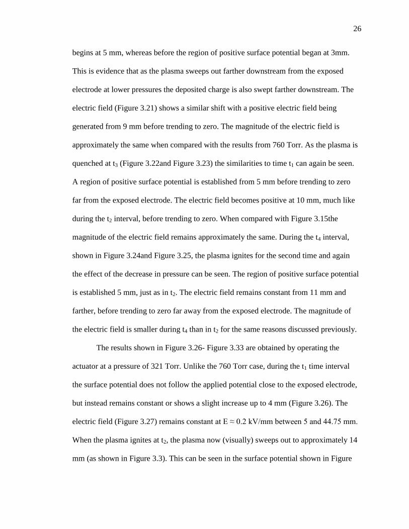
begins at 5 mm, whereas before the region of positive surface potential began at 3mm.
This is evidence that as the plasma sweeps out farther downstream from the exposed
electrode at lower pressures the deposited charge is also swept farther downstream. The
electric field (Figure 3.21) shows a similar shift with a positive electric field being
generated from 9 mm before trending to zero. The magnitude of the electric field is
approximately the same when compared with the results from 760 Torr. As the plasma is
quenched at t3 (Figure 3.22and Figure 3.23) the similarities to time t1 can again be seen.
A region of positive surface potential is established from 5 mm before trending to zero
far from the exposed electrode. The electric field becomes positive at 10 mm, much like
during the t2 interval, before trending to zero. When compared with Figure 3.15the
magnitude of the electric field remains approximately the same. During the t4 interval,
shown in Figure 3.24and Figure 3.25, the plasma ignites for the second time and again
the effect of the decrease in pressure can be seen. The region of positive surface potential
is established 5 mm, just as in t2. The electric field remains constant from 11 mm and
farther, before trending to zero far away from the exposed electrode. The magnitude of
the electric field is smaller during t4 than in t2 for the same reasons discussed previously.
The results shown in Figure 3.26- Figure 3.33 are obtained by operating the
actuator at a pressure of 321 Torr. Unlike the 760 Torr case, during the t1 time interval
the surface potential does not follow the applied potential close to the exposed electrode,
but instead remains constant or shows a slight increase up to 4 mm (Figure 3.26). The
electric field (Figure 3.27) remains constant at E ≈ 0.2 kV/mm between 5 and 44.75 mm.
When the plasma ignites at t2, the plasma now (visually) sweeps out to approximately 14
mm (as shown in Figure 3.3). This can be seen in the surface potential shown in Figure

27
3.28. Like the 760 Torr case, there is a region in which the dielectric surface acquires an
always net positive surface potential starting at 7.5 mm and continuing over the entire
dielectric surface. The electric field during this time interval (Figure 3.29) becomes
positive at 20 mm and is relatively constant at E ≈ 0.1 kV/mm. When the plasma again
quenches, similar trends emerge that were seen during t1. The surface potential (Figure
3.30) becomes positive at 13 mm and reaches a maximum value of 3.5 kV before
trending to zero. The electric field (Figure 3.31) during this time interval remains
constant over all time slices after 20 mm. At positions closer to the exposed electrode (x
< 5 mm) the electric field increases at first (up to 2.5 mm) before entering a region of
negative electric field between 5 and 22.5 mm. When the plasma ignites for the second
time (Figure 3.32 and Figure 3.33) there is a positive, non-zero surface potential between
12.5 and 40 mm, similar to that of t2. The electric field during this time interval oscillates
from zero and 0.05 kV/mm between 20 and 44.75 mm. Note that the overall electric field
strength is weaker at this pressure when compared to the 760 Torr case discussed
previously.

28
Figure 3.10: Potential on the surface of the dielectric between t1 and t2 at 760 Torr.
Figure 3.11: Electric field near the dielectric surface between t1 and t2 at 760 Torr.

29
Figure 3.12: Potential on the surface of the dielectric between t2 and t3 at 760 Torr.
Figure 3.13: Electric field near the dielectric surface between t2 and t3 at 760 Torr.

30
Figure 3.14: Potential on the surface of the dielectric between t3 and t4 at 760 Torr.
Figure 3.15: Electric field near the dielectric surface between t3 and t4 at 760 Torr.

31
Figure 3.16: Potential on the surface of the dielectric after t4 at 760 Torr.
Figure 3.17: Electric field near the dielectric surface after t4 at 760 Torr.

32
Figure 3.18: Potential on the surface of the dielectric between t1 and t2 at 429 Torr.
Figure 3.19: Electric field near the dielectric surface between t1 and t2 at 429 Torr.

33
Figure 3.20: Potential on the surface of the dielectric between t2 and t3 at 429 Torr.
Figure 3.21: Electric field near the dielectric surface between t2 and t3 at 429 Torr.
34
Figure 3.22: Potential on the surface of the dielectric between t3 and t4 at 429 Torr.
Figure 3.23: Electric field near the dielectric surface between t3 and t4 at 429 Torr.

35
Figure 3.24: Potential on the surface of the dielectric after t4 at 429 Torr.
Figure 3.25: Electric field near the dielectric surface after t4 at 429Torr.

36
Figure 3.26: Potential on the surface of the dielectric between t1 and t2 at 321 Torr.
Figure 3.27: Electric field near the dielectric surface between t1 and t2 at 321 Torr.

37
Figure 3.28: Potential on the surface of the dielectric between t2 and t3 at 321 Torr.
Figure 3.29: Electric field near the dielectric surface between t2 and t3 at 321 Torr.

38
Figure 3.30: Potential on the surface of the dielectric between t3 and t4 at 321 Torr.
Figure 3.31: Electric field near the dielectric surface between t3 and t4 at 321 Torr.

39
Figure 3.32: Potential on the surface of the dielectric after t4 at 321 Torr.
Figure 3.33: Electric field near the dielectric surface after t4 at 321 Torr.
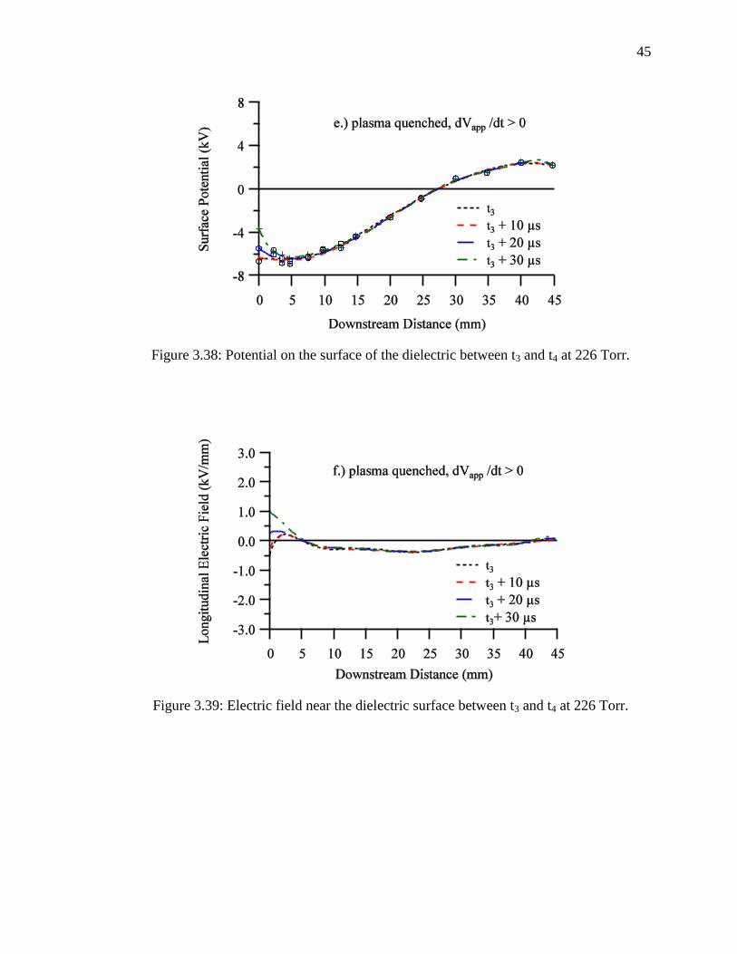
Plotted in Figure 3.34- Figure 3.41 are the results of operating the actuator at a
pressure of 226 Torr. During t1 the surface potential exhibits all of the previously
discussed trends and, like the results at 321 Torr, increases up to a distance of 10 mm. At

40
this pressure, however, the surface potential never goes to zero and always has a value of
2 kV or greater. The electric field (Figure 3.35) is uniform over the entire dielectric
surface (except at 7 mm or less) at a magnitude of E ≈ 0.1 kV/mm before going to zero at
40 mm. When the plasma ignites at t2 (Figure 3.36) the spread of surface potential
between time slices is larger than the previously discussed pressures. The potential
increases up to a value of 6 kV and after 15 mm is always positive and non-zero. The
corresponding electric field is approximately constant after 10 mm, varying slightly
between zero and 0.10 kV/mm. During time t3 similar trends discussed for t1 are seen in
the surface potential. The region of positive potential is established after 27.5 mm
whereas at 321 Torr the region of positive surface potential was established at a distance
of 15 mm. The electric field at this time shows similar trends to those discussed for
Figure 3.35. Here, however, the electric field is constant from 7 mm to 30 mm with E ≈ -
0.3 kV/mm. The electric field never returns to a positive value before going to zero at
44.75 mm. This is the first time that the electric field is largely negative over the entirety
of the dielectric surface. When the plasma ignites for the second time, a region of
constant positive surface potential is established at 27.5 mm. The surface potential never
goes to zero far away from the exposed electrode edge, maintaining a value of 2 kV at
44.75 mm while the electric field is largely negative between 10 mm and 35 mm.
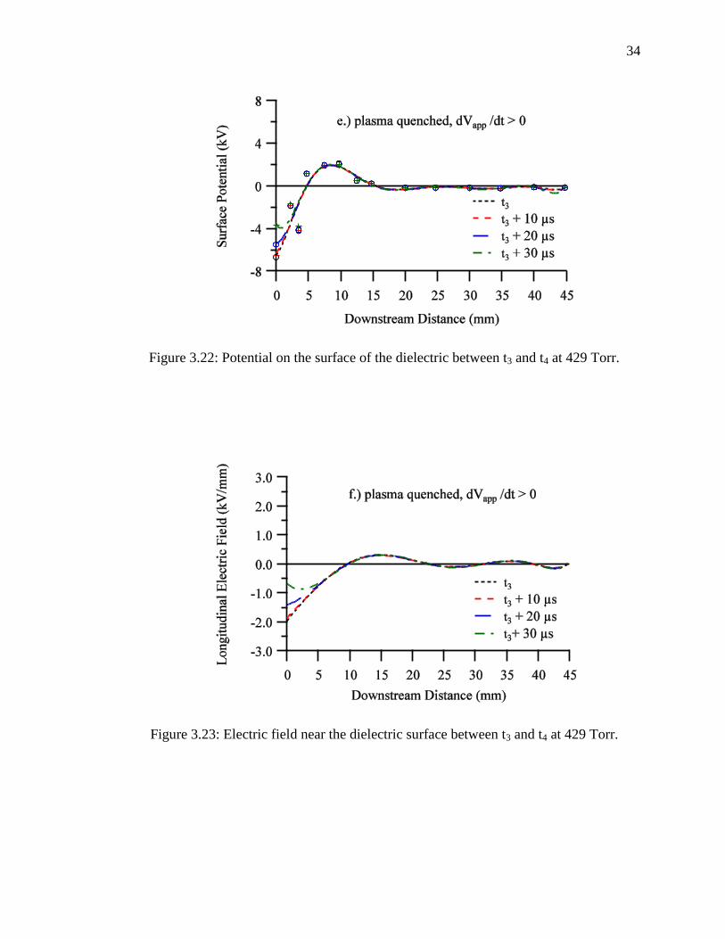
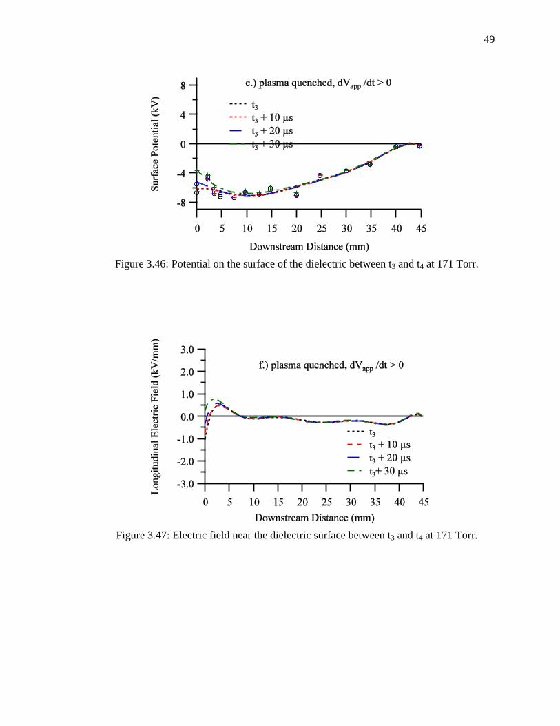
When the plasma is quenched during t1 at a pressure of 171 Torr (Figure 3.42 and
Figure 3.43) the surface potential remains constant at 6 kV out to a distance of 20 mm
before beginning to decrease. The electric field is approximately zero from 5 mm until
the end of the buried electrode. A local maximum of E = 0.2 kV/mm at a downstream
distance of 25 mm is seen, but this is an artifact of the fitting routine used on the data.

41
Once the plasma ignites the effect the plasma has on sweeping the charge across the
dielectric surface is readily seen (Figure 3.44). A region of always positive surface
potential is established at 30 mm. The electric field (Figure 3.45) remains mostly constant
throughout this time interval, oscillating between 0.5 kV/mm and -0.5 kV/mm. At t3 there
is never a region on the dielectric surface where the surface potential (Figure 3.46) is
always positive. The electric field exhibits a local maximum at 2.5 mm downstream, but
then trends to zero. The electric field between 6 and 17 mm is approximately zero before
going negative between 17 and 44.75 mm (see Figure 3.47). Between all of the time
intervals the surface potential, as well as the electric field, does not vary much. In Figure
3.48 and Figure 3.49 the effect the plasma has on the distribution of the surface potential
is seen again. During each time step between 10 and 30 mm, the surface potential
remains constant. The electric field decreases from 1.5 kV/mm to zero by 5 mm and
remains approximately zero over the entirety of the dielectric surface.
At a pressure of 88 Torr, the same trends when the actuator is operating at a
pressure of 171 Torr are seen during each of the time intervals. During t1 (Figure 3.50 and
Figure 3.51) there is a region between 5 and 25 mm that has a constant surface potential
of 6 kV. The electric field during this time interval is zero after 5 mm. Similar trends to
that shown at 171 Torr are seen again as the plasma ignites at t2 (Figure 3.52 and Figure
3.53).When the plasma quenches again at t3 (Figure 3.54 and Figure 3.55) the surface
potential is constant at -6 kV over nearly all of the dielectric surface, only beginning to
increase at a downstream location of 35 mm. Just like in the case of 171 Torr, there is no
region of positive surface potential that is established on the dielectric surface. Again, the
electric field has a non-zero value only close to the exposed electrode edge before going

42
to zero at 10 mm. Once the plasma forms for the second time (Figure 3.56 and Figure
3.57) the plasma sweeps the charge across the dielectric, remaining constant for each
time interval between 5 and 45 mm. At t4 + 10 µs the surface potential remains positive
across the dielectric surface, with an approximately constant value of 1.75 kV. The
electric field exhibits similar behavior as that shown in the time interval of t2.
Polarization effects are seen close to the exposed electrode edge, but the majority of the
dielectric surface experiences an electric field of zero. The electric field does take on a
small negative magnitude at 35 mm, however the overall trend cannot be captured due to
the lack of V-dot probes after 44.75 mm.

43
Figure 3.34: Potential on the surface of the dielectric between t1 and t2 at 226 Torr.
Figure 3.35: Electric field near the dielectric surface between t1 and t2 at 226 Torr.

44
Figure 3.36: Potential on the surface of the dielectric between t2 and t3 at 226 Torr.
Figure 3.37: Electric field near the dielectric surface between t2 and t3 at 226 Torr.
45
Figure 3.38: Potential on the surface of the dielectric between t3 and t4 at 226 Torr.
Figure 3.39: Electric field near the dielectric surface between t3 and t4 at 226 Torr.

46
Figure 3.40: Potential on the surface of the dielectric after t4 at 226 Torr.
Figure 3.41: Electric field near the dielectric surface after t4 at 226 Torr.

47
Figure 3.42: Potential on the surface of the dielectric between t1 and t2 at 171 Torr.
Figure 3.43: Electric field near the dielectric surface between t1 and t2 at 171 Torr.

48
Figure 3.44: Potential on the surface of the dielectric between t2 and t3 at 171 Torr.
Figure 3.45: Electric field near the dielectric surface between t2 and t3 at 171 Torr.
49
Figure 3.46: Potential on the surface of the dielectric between t3 and t4 at 171 Torr.
Figure 3.47: Electric field near the dielectric surface between t3 and t4 at 171 Torr.

50
Figure 3.48: Potential on the surface of the dielectric after t4 at 171 Torr.
Figure 3.49: Electric field near the dielectric surface after t4 at 171 Torr.

51
Figure 3.50: Potential on the surface of the dielectric between t1 and t2 at 88 Torr.
Figure 3.51: Electric field near the dielectric surface between t1 and t2 at 88 Torr.

52
Figure 3.52: Potential on the surface of the dielectric between t2 and t3 at 88 Torr.
Figure 3.53: Electric field near the dielectric surface between t2 and t3 at 88 Torr.

53
Figure 3.54: Potential on the surface of the dielectric between t3 and t4 at 88 Torr.
Figure 3.55: Electric field near the dielectric surface between t3 and t4 at 88 Torr.

54
Figure 3.56: Potential on the surface of the dielectric after t4 at 88 Torr.
Figure 3.57: Electric field near the dielectric surface after t4 at 88 Torr.

55
3.3. AVERAGE SURFACE POTENTIAL AND CHARGE TRANSFERRED
To better understand how the surface potential is distributed across the dielectric
surface the average surface potential at each V-dot probe location was calculated. This is
done by taking the average over a set number of applied AC signals (in this experiment, 4
periods) after equilibrium has been established. The results of this analysis are shown in
Figure 3.58 - Figure 3.63 with error bars where appropriate. Similar conditions to those
found in [24] are used in this work as the same material (Macor) was used as the
dielectric material, as well as similar high voltage signals (13.4 kVpk-pk 5 kHz sine wave
in [24] ). Figure 3.58 shows that at 760 Torr the surface potential reaches a maximum
value of 2.5 kV at a downstream location of 6.00 mm. Enloe et al. found that for similar
conditions the largest surface potential is 1.67 kV at approximately 7.5 mm downstream
[24]. At pressures of 429, 321, and 226 Torr the maximum average surface potential
reaches a value of 3.0 kV at positions of x = 15, 20, and 40 mm, respectively. This shows
that as the pressure decreases the region of largest surface potential moves farther
downstream from the exposed electrode. During this same span of pressure drops, the
width of the average surface potential also grows. At 760 Torr, there is a region of net
positive potential from the exposed electrode edge 20.00 mm downstream. This region
extends to 35 mm at 429 Torr until reaching the end of the V-dot probe array at 44.75
mm by 321 Torr. The entire dielectric surface maintains the net positive average surface
potential at pressures of 171 Torr and 88 Torr.
Looking at Figure 3.62 and Figure 3.63, there is no peak surface potential
downstream, indicating that the location of the peak surface potential has moved so far
downstream that our V-dot probes are no longer able to capture it. Interestingly though,
these plots do exhibit the smaller peak close to the exposed electrodes edge that begins to
56
appear at 321 Torr. This local maximum is always located at approximately 2.5 mm
downstream, regardless of the ambient pressure conditions. The amplitude of the
maximum, however, is varied having a range of values of 0.75 kV, 0.45 kV, 0.6 kV, and
1.75 kV corresponding to the pressures from 321 Torr down to 88 Torr, respectively.
The results shown in Figure 3.64- Figure 3.69 depict how the average physical
charge is deposited downstream as the ambient pressure is changed. Much like the
average surface potential, the maximum charge transferred moves downstream as
pressure decreases. In fact, the location for the peak charge transferred corresponds
directly to the location of the peak average surface potential at a given pressure. This is to
be expected as the contributions from the capacitive voltage division/polarization effects
diminish far from the electrodes edge, meaning the only meaningful mechanism for
building up surface potential is through physical charge deposition.
3.4. ION DENSITY
Assuming a linear relationship between light intensity and ion density, we use
time-averaged photographs of the plasma to obtain a qualitative measurement of the ion
density variation with pressure and downstream distance. A Canon PowerShot SX200IS
with a shutter speed of 1/3 s and an ISO setting of 800 allows for time averaged
photographs to be taken (such as those previously shown in Figure 3.3). These photos are
converted to a gray scale value and normalized such that they can be compared directly to
one another. In this way a value for light intensity, and subsequently ion density, can be
obtained at all downstream locations. The results of this analysis can be seen in Figure
3.70. The highest density plasma is made at the exposed electrode edge at a pressure of

57
88 Torr. In fact, the densest region of plasma formation for a given pressure is always
within 0.4 mm of the exposed electrode edge. The large spike next to the exposed
electrode represents a region of intense microdischarges [14].
Figure 3.58: Average surface potential at 760 Torr.

58
Figure 3.59: Average surface potential at 429 Torr.
Figure 3.60: Average surface potential at 321 Torr.

59
Figure 3.61: Average surface potential at 226 Torr.
Figure 3.62: Average surface potential at 171 Torr.

60
Figure 3.63: Average surface potential at 88 Torr.
Figure 3.64: Average charge transferred at 760 Torr.

61
Figure 3.65: Average charge transferred at 429 Torr.
Figure 3.66: Average charge transferred at 321 Torr.

62
Figure 3.67: Average charge transferred at 226 Torr.
Figure 3.68: Average charge transferred at 171 Torr.

63
Figure 3.69: Average charge transferred at 88 Torr.
Figure 3.70: Calculating the normalized light intensity allows for the determination of a
qualitative measurement for the ion density at any downstream location.

64
4. DISCUSSION
The overall trends and effects that ambient pressure has on the surface potential of
the dielectric, generated electric field, and average force production of the plasma
actuator are discussed here.
4.1. SURFACE POTENTIAL AND CHARGE BUILD-UP
As shown in Figure 4.1, the maximum charge transferred moves downstream as
pressure decreases in similar fashion to the average surface potential. Only those
pressures down to 226 Torr are plotted due to the fact that at lower pressures the
maximum average surface potential has moved past our farthest V-dot probe. The
polarization effect that contributes to the overall surface potential is mainly seen at
downstream distances of 2.5 mm or less, where the electric field is the strongest. This
means that the dominant mechanism for building surface potential at downstream
distances that are far from the leading edge of the exposed electrode is physical charge
deposition. Finally, the maximum average surface potential and charge transferred are
inversely proportional to the pressure.
4.2. LOCATION OF PLASMA PRODUCTION
Body force produced by a plasma actuator is directly proportional to the number
of plasma ions present and the strength of the electric field where those ions are produced
(Eq. (1)). By integrating each curve in Figure 3.70, it is possible to qualitatively
determine the quantity of plasma present for a given operating pressure. The normalized

65
results are shown in Figure 4.2. As is shown, there is 20 times more plasma produced at
88 Torr than at 760 Torr. This increase is inversely proportional to the ambient pressure.
It is also interesting to examine the electric field in the region where the plasma is
created. By combining the plasma extent measurements (Figure 3.3) with the electric
field data presented in Figure 3.10-Figure 3.57, it is possible to determine the fraction of
the plasma extent with no electric field. The results of this analysis are also shown in
Figure 4.2.
Figure 4.1: The location of the maximum average surface potential and charge transferred
moves downstream as pressure decreases in a similar non-linear fashion as Figure 3.2.
From 760 to 321 Torr all plasma is created in a region where the electric field has
some non-zero magnitude. As pressure is decreased further this trend changes

66
significantly. For the tested pressures of 226, 171, and 88 Torr, 38, 74, and 88 percent of
the plasma is created in regions of approximately zero electric field, respectively. While
there is 20 times more plasma present at 88 Torr than at 760 Torr, 88 percent of the
plasma is in a region where there is no electric field present to accelerate it.
Figure 4.2: As pressure decreases a larger percentage of plasma is formed where the
electric field is approximately zero.
4.3. QUALITATIVE FORCE TRENDS
With the data presented in this paper it is possible to calculate the qualitative
average body force that the plasma actuator produces. In order to calculate the force
produced by our plasma actuator the electric field results are averaged with respect to
time. A spatial average of the combined electric field and ion density is performed to

67
obtained the qualitative time-average force. This is done in order to multiply the spatial
electric field data with the qualitative spatial ion density measurements. These
calculations are compared with measurements presented in [19] and recreated in Figure
4.3. This work is used for comparison due to similar operating parameters (shape,
frequency, and amplitude of the sine wave) and the number of pressures that were tested.
A direct comparison cannot be made between this work and [19] due to differences in
how force is calculated/measured, however, a similar qualitative trend is still evident
between the two experiments. Looking at Figure 4.3 it is evident that there is a local
maximum force produced around 600 Torr for an exposed electrode thickness of 0.2 mm.
While this work cannot conclusively confirm this, it is possible to say that the force does
increase between 760 and 429 Torr before beginning to decrease. Overall, the two
separate works show good agreement as the pressure is decreased, with an initial increase
in force before decreasing and trending to zero.
It is worthwhile to now compare the calculated force for the current plasma
actuator and the power consumption. Looking again at Figure 3.2 and comparing with the
force production shown in Figure 4.3 it is possible to make some comments about how
the power consumed is being used by the plasma actuator. Looking at the region of
pressures between 226 and 88 Torr and the corresponding power consumption at those
pressures we see that although the power consumption is increasing, the force production
is decreasing. This is further evidence that as pressure is decreased, more power is being
used in processes not related to force production. Since the mechanism for force
production comes from the momentum coupling that occurs due to the acceleration of the
plasma and since the electric field (the accelerating source of the ions) has been measured

68
and calculated to be zero far from the exposed electrode edge where large amounts of
plasma are formed, it is now possible to say that the increased power consumption is for
generating plasma and not accelerating it.
Figure 4.3: The space and time average force for this work shows similar trends to that of
the force measured by Abe et al. [19].

69
5. CONCLUSION
In this paper measurements done with an array of capacitive V-dot probes of the
potential on the dielectric surface have been presented. While the surface potential is
spread out across the dielectric surface as pressure decreases, the electric field only
exhibits a slight decrease in magnitude close to the exposed electrode edge. As pressure
is decreased from 760 to 88 Torr up to 20 times more plasma becomes available for
acceleration, and thus force production. At lower pressures, however, up to 88 percent of
the plasma is created in a region where there is an effective electric field strength of zero.
Because the acceleration of the plasma ions is the means for force production it follows
that this is why force production trends to zero as pressure is decreased. The average
force calculations further show this trend with an initial increase in force production
before trending to zero. This suggests that there is an optimum amount of plasma, and
thus an optimum pressure, to operate the plasma actuator at in order to produce the
maximum amount of force. These trends are in good agreement with those presented in
the literature [19]. By looking at the plasma extent, power consumption, and force
production at a given pressure it is possible to conclude that at low pressures (226 Torr
and below) more power is going into creating plasma than accelerating it.
Future work on SDBD plasma actuators operating at high altitude should focus on
resolving the spatiotemporal evolution of the force produced. Using a high speed camera
with an appropriate sensor would do well to temporally resolve the ion density which
could then be multiplied with the temporally resolved electric field calculated in this
paper.

70
APPENDIX A.
MISCELLANEOUS PLOTS

71
Figure A.1: Average surface potential for each individual trial ran at 760 Torr.
Figure A.2: Average surface potential for each individual trial ran at 429 Torr.

72
Figure A.3: Average surface potential for each individual trial ran at 321 Torr.
Figure A.4: Average surface potential for each individual trial ran at 226 Torr.

73
Figure A.5: Average surface potential for each individual trial ran at 171 Torr.
Figure A.6: Average surface potential for each individual trial ran at 88 Torr.

74
Figure A.7: Plot of the normalized number of ions
Figure A.8: Current density for probes 2-5 at 760 Torr.

75
Figure A.9: Current density for probes 6-9 at 760 Torr.
Figure A.10: Current density for probes 10-14 at 760 Torr.

76
Figure A.11: Current density for probes 2-5 at 429 Torr.
Figure A.12: Current density for probes 6-9 at 429 Torr.

77
Figure A.13: Current density for probes 2-5 at 321 Torr.
Figure A.14: Current density for probes 6-9 at 321 Torr.

78
Figure A.15: Current density for probes 10-14 at 321 Torr.
Figure A.16: Current density for probes 2-5 at 226 Torr.

79
Figure A.17: Current density for probes 6-9 at 226 Torr.
Figure A.18: Current density for probes 10-14 at 226 Torr.

80
Figure A.19: Current density for probes 2-5 at 171 Torr.
Figure A.20: Current density for probes 6-9 at 171 Torr.

81
Figure A.21: Current density for probes 10-14 at 171 Torr.
Figure A.22: Current density for probes 10-14 at 88 Torr.

82
Figure A.23: Current density for probes 6-9 at 88 Torr.
Figure A.24: Current density for probes 10-14 at 88 Torr.

83
APPENDIX B.
DETAILED TROUBLESHOOTING OF EXPERIMENTAL SETUP

84
In this appendix a detailed guide to troubleshooting and setting up the high
altitude plasma actuator experiment is given.
B.1. HIGH VOLTAGE PASSTHROUGH AND HIGH VOLTAGE WIRE
The high voltage pass-through and high voltage wire shown in Figure B.1 are
used in this experiment for a number of reasons. The first reason is due to arcing. At
standard atmospheric pressure a lower gauge, less insulated wire can be used, however,
when operating at lower pressures it is recommended a wire such as the E76475 from
Thermal Wire and Cable Corp. be used. This wire is rated to 40 kV DC and helps to
reduce the chance of arcing at low pressures. If a thinner, lower voltage rating wire is
used plasma can form within the wire itself.
The high voltage pass-through used on the bell jar is a lab made pass-through.
Commercial pass-throughs are available, however, they do not provide for enough
insulation against arcing between the pass-through itself and the vacuum chamber.
Because of this the high voltage wire is run through the pass through and connected to the
plasma actuator in one continuous piece. This allows for the insulation on the high
voltage wire to remain intact from the high voltage transformer all the way to the plasma
actuator. The pass through itself is made to fit the vacuum chamber from some scrap
acrylic. Once the bolt hole pattern is drilled into the material a center hole is made such
that the high voltage wire can fit through. A middle section of the insulation is cut away
such that the bare wire sits inside of the center drilled hole. This is to allow separation
between the inside of the chamber and out so that good vacuum can be sealed. This is
also to help keep plasma from forming within the wire as well. The final step in

85
construction is to use some JB Weld to seal the hole. This grey substance can be seen in
Figure B. 1.
Figure B.1: The custom made high voltage pass-through used for high altitude
testing.
Within the vacuum chamber it is necessary to take care of where the high voltage
wire lays. As shown in Figure B.2 a suspension system of Kapton tape is used to keep the
high voltage wire a sufficient distance from the vacuum chamber. If the wire is touching
or in close proximity to the chamber walls arcing will occur creating undesired plasma
formation. Also note in Figure B.2 the amount of Kapton tape used on the high voltage
wire near the pass through area in the back of the chamber. Again, this is to prevent
plasma formation between the wire and walls as this is the closest point to the chamber
walls that the wire will be.

86
Figure B.2: Special care must be taken to insure that arcing does not occur
between the high voltage wire and the vacuum chamber walls.
B.2. HIGH VOLTAGE TRANSFORMER CONSIDERATIONS
In order to prevent undesired operation of the plasma actuator a faraday cage must
be built around the high voltage transformer used for this experiment. This is shown in
Figure B.3 . The large leads on the transformer are capable of picking up ambient noise in
the lab causing plasma to form on the actuator without the function generator operating.
The faraday cage is able to shield out this noise which is approximately 16 kHz and most
likely comes from the overhead lights. The high voltage probe is also placed inside of this
faraday cage housing. Special care must be taken when running the high voltage wire out
of the faraday cage to the vacuum chamber. This is due to the fact that the faraday cage
must be grounded in order to function properly. If the high voltage wire is located too
close to the grounded copper mesh arcing will occur. Kapton tapes as well as standoffs
are used to further insulate and position the wire away from the grounded cage.
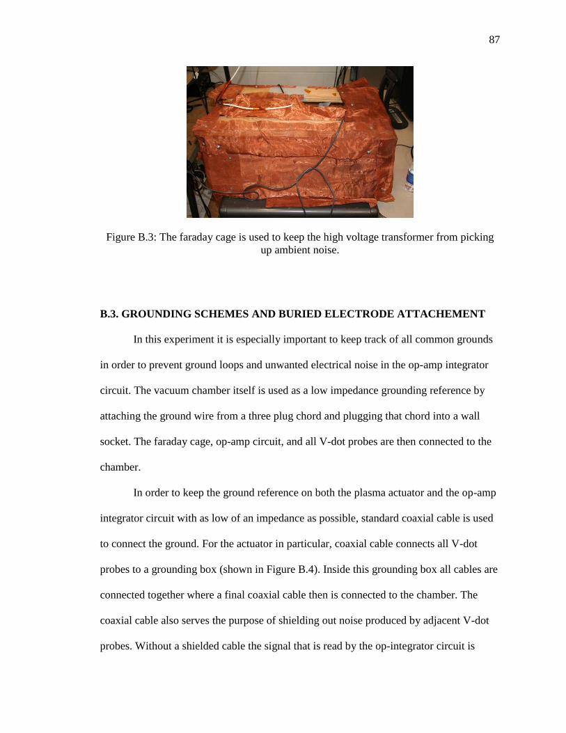
87
Figure B.3: The faraday cage is used to keep the high voltage transformer from picking
up ambient noise.
B.3. GROUNDING SCHEMES AND BURIED ELECTRODE ATTACHEMENT
In this experiment it is especially important to keep track of all common grounds
in order to prevent ground loops and unwanted electrical noise in the op-amp integrator
circuit. The vacuum chamber itself is used as a low impedance grounding reference by
attaching the ground wire from a three plug chord and plugging that chord into a wall
socket. The faraday cage, op-amp circuit, and all V-dot probes are then connected to the
chamber.
In order to keep the ground reference on both the plasma actuator and the op-amp
integrator circuit with as low of an impedance as possible, standard coaxial cable is used
to connect the ground. For the actuator in particular, coaxial cable connects all V-dot
probes to a grounding box (shown in Figure B.4). Inside this grounding box all cables are
connected together where a final coaxial cable then is connected to the chamber. The
coaxial cable also serves the purpose of shielding out noise produced by adjacent V-dot
probes. Without a shielded cable the signal that is read by the op-integrator circuit is

88
noisier as well as larger in magnitude, both are adverse to the measurements trying to be
made.
Figure B.4: Coaxial cable is used to ground each V-dot probe to a common point in a
grounding box.
As an additional rule of thumb it is always good practice in this experiment to
plug all electronics into the same power strip. In this case that would mean that the
function generator, audio amplifier, and oscilloscope all need to be plugged into the same
place. This helps to eliminate another possible ground loop.
In Figure B.4 it is also worthwhile to note the way the buried electrode is attached
to the back of the Macor sheet. The V-dot probe array is laid flat against the Macor such
that no air gap exists between it and the Macor. If there is an air gap not only can plasma
form in this region, but the measurements of the surface potential from the V-dot probes
will be inaccurate as well due to the fact that there is now a second dielectric to account
for. Kapton tape is used to keep the buried electrode in the proper place.

89
B.4. ADDITIONAL OP-AMP INTEGRATOR COMMENTS
Shown in Figure B.5 is the actual op-amp integrator circuit used for this
experiment. The op-amp is run off of four, nine volt batteries(two batteries wired together
per side). Across the power inputs filter capacitors are used (small blue capacitors in
Figure B.5) in order to keep noise from leaking into the high frequency signal that is
being measured. To measure the output on the oscilloscope a simple Tektronix P2221
voltage probe is used in 1X mode. As a precaution against picking up the same 16 kHz
noise that the transformer can pick up, a faraday cage was built around the circuit. This,
however, improved the signal an immeasurable amount and is thus unnecessary.
Figure B.5: The op-amp integrator circuit used in this experiment.

90
BIBLIOGRAPHY
1. C.L. Enloe, G.I.F., T.E. McLaughlin, Robert D. VanDyken, K.D. Kachner, Eric J.
Jumper, and Thomas C. Corke, Mechanisms and Responses of a Single Dielectric Barrier
Plasma Actuator: Plasma Morphology. AIAA Journal, 2004. 42(3): p. 6.
2. Moreau, E., Airflow control by non-thermal plasma actuators. Journal of Physics
D: Applied Physics, 2007(40): p. 33.
3. Jerome Pons, E.M.a.G.T., Asymmetric surface dielectric barrier discharge in air at
atmospheric pressure: electrical properties and induced airflow characteristics. Journal Of
Physics D: Applied Physics, 2005. 38: p. 9.
4. Thomas C. Corke, C.L.E., and Stephen P. Wilkinson, Dielectric Barrier Discharge
Plasma Actuators for Flow Control. Annual Review of Fluid Mechanics, 2009. 42: p. 27.
5. Corke, M.L.P.T.C., Separation control on high angle of attack airfoil using plasma
actuators. AIAA Journal, 2004. 42: p. 8.
6. Corke, C.H.T.C., Plasma Flaps and Slats: An Application of Weakly Ionized
Plasma Actuators. Journal of Aircraft, 2009. 46(3): p. 10.
7. Post, T.C.C.M.L., Overview of Plasma Flow Control: Concepts, Optimization,
and Applications. 43rd AIAA Aerospace Sciences Meething and Exhibit, 2005: p. 15.
8. Mertz, T.C.C.B., Plasma Flow Control Optimized Airfoil. 44th AIAA Aerospace
Sciences Meething and Exhibit, 2006: p. 13.
9. Mehul P. Patel, T.T.N., Srikanth Vasudevan, Plasma Actuators for Hingeless
Aerodynamic Control of an Unmanned Air Vehicle. 3rd AIAA Flow Control Conference,
2008: p. 21.
10. Flint O. Thomas, T.C.C., Muhammad Iqbal, Alexey Kozlov, David Schatzman,
Optimization of Dielectric Barrier Discharge Plasma Actuators for Active Aerodynamic
Flow Control. AIAA Journal, 2009. 47(9): p. 10.
11. M. Forte, J.J., J. Pons, E. Moreau, G. Touchard, M. Cazalens, Optimization of a
dieletric barrier discharge actuator by stationary and non-stationary measurements of the
induced flow velocity: application to airflow control. Exp. Fluids, 2007. 43: p. 12.
12. J. Reece Roth, X.D., Optimization of the Aerodynamic Plasma Actuator as an
Electrohydrodynamic (EHD) Electrical Device. 44th AIAA Aerospace Sciences
Meething and Exhibit, 2008: p. 28.

91
13. Ryan Durscher, S.R., Novel Multi-Barrier Plasma Actuators for Increased Thrust.
48th AIAA Aerospace Scieneces Meeting and Exhibit Including the New Horizons
Forum and Aerospace Exposition, 2010: p. 9.
14. James W. Gregory, C.L.E., Gabriel I. Font, and Thomas E. McLaughlin, Force
Production Mechanisms of a Dielectric-Barrier Discharge Plasma Actuator, in 45th
AIAA Aerospace Sciences Meeting and Exhibit, `, Editor. 2007, AIAA 2007-185: Reno,
Nevada. p. 13.
15. V.M. Litvinov, V.V.S., and A.A. Uspenskii, Role of the Static Pressure in
Experiments on Flow Control by Means of Surface Capacitor Discharges. Fluid
Dynamics, 2006. 41(2): p. 6.
16. N. Benard, N.B., and E. Moreau, Electric Wind Produced by a Single Dielectric
Barrier Discharge Actuator Operating in Atmospheric Flight Conditions - Pressure
Outcome. 39th Plasmadynamics and Lasers Conference, 2008: p. 16.
17. N. Benard, N.B.a.E.M., Electric wind produced by a surface dielectric barrier
dishcarge operating in air at different pressures: aeronautical control insights. Journal of
Physics D: Applied Physics 2008. 41: p. 5.
18. Yun Wu, Y.L., Min Jia, Huimin Song, Zhigang Guo, Ximing Zhu, and Yikang
Pu, Influence of operating pressure on surface dielectric barrier discharge plasma
aerodynamic actuation characteristics. Applied Physics Letters, 2008. 93: p. 3.
19. Takashi Abe, Y.T., Shunichi Sato, and Nobara Kimura, Experimental Study for
Momentum Transfer in a Dielectric Barrier Discharge Plasma Acutator. AIAA Journal,
2008. 46(9): p. 9.
20. N. Benard, E.M., Effects of Altitude on the Electromechanical Characteristics of a
Single Dielectric Barrier Discharge Plasma Actuator. 41st Plasmadynamics and Lasers
Conference, 2010: p. 17.
21. Philippe Versailles, V.G.-G., and Huu Duc Vo, Impact of Pressure and
Temperature on the Performance of Plasma Actuators. AIAA, 2010. 48(4): p. 5.
22. C.L. Enloe, M.G.M., and T.E. McLaughlin, Time-correlated force production
measurements of the dielectric discharge plasma aerodynamic actuator. Journal of
Applied Physics, 2008. 103(073302): p. 7.
23. C.L. Enloe, T.E.M., J.W. Gregory, R.A. Medina, and W.S. Miller, Surface
Potential and Electric Field Structure in the Aerodynamic Plasma Acutator, in 46th AIAA
Aerospace Sciences Meeting and Exhibit. 2008, AIAA 2008-1103: Reno, Nevada. p. 11.

92
24. C.L. Enloe, G.I.F., T.E. McLaughlin, and D.M. Orlov Surface Potential and
Longitudinal Electric Field Measurements in the Aerodynamic Plasma Actuator. AIAA
Journal, 2008. 46(11): p. 11.
25. G.I. Font, C.L.E., T.E. McLaughlin, and D. Orlov, Plasma Discharge
Characteristics and Experimentally Determined Boundary Conditions for a Plasma
Actuator, in 45th AIAA Aerospace Sciences Meeting. 2007, AIAA 2007-0188: Reno,
Nevada. p. 14.
26. Dmitry F. Opaits, G.N., Sohail H. Zaidi, Mikhail N. Schneider, Richard B. Miles,
Alexandre V. Likhanskii, Sergey O. Macheret, DBD Plasma Actuators Driven by a
Combination of Low Frequency Bias Voltage and Nanosecond Pulses. 48th AIAA
Aerospace Scieneces Meeting and Exhibit, 2008(AIAA 2008-1372): p. 18.
27. T.G. Nichols, J.L.R., Fundamental Processes of DBD Plasma Actuators Operating
at High Altitude. 50th Annual AIAA Aerospace Sciences Meeting, 2012: p. 23.

93
VITA
Timothy Nichols was born in Covington, Tennessee to Tina and Sam Nichols. He
graduated 1st in his class from Greenbrier High School in May 2006 after which he
pursued at Physics degree at Hendrix College in Conway, AR. Upon completion of his
undergraduate degree he attended the Missouri University of Science and Technology to
obtain a Master’s degree in Aerospace Engineering. Throughout his academic career,
Timothy has been a member of numerous academic honor societies and organizations
including: the Society of Physics Students, Pi Mu Epsilon, and AIAA.
When not pursuing academic interests, Timothy gets out and enjoys nature as
much as possible. He goes rock climbing, hiking, canoeing, and camping any chance he
gets. He is also very interested in playing numerous different sports (basketball, baseball,
soccer, racquetball, etc.) and living an overall healthy and active lifestyle.