Embed Size (px)
Citation preview
HAL Id: hal-00646325https://hal.archives-ouvertes.fr/hal-00646325
Submitted on 29 Aug 2013
HAL is a multi-disciplinary open accessarchive for the deposit and dissemination of sci-entific research documents, whether they are pub-lished or not. The documents may come fromteaching and research institutions in France orabroad, or from public or private research centers.
L’archive ouverte pluridisciplinaire HAL, estdestinée au dépôt et à la diffusion de documentsscientifiques de niveau recherche, publiés ou non,émanant des établissements d’enseignement et derecherche français ou étrangers, des laboratoirespublics ou privés.
Operating mechanism of the organicmetal-semiconductor field-effect transistor (OMESFET)
Chang Hyun Kim, Denis Tondelier, Bernard Geffroy, Yvan Bonnassieux,Gilles Horowitz
To cite this version:Chang Hyun Kim, Denis Tondelier, Bernard Geffroy, Yvan Bonnassieux, Gilles Horowitz. Operatingmechanism of the organic metal-semiconductor field-effect transistor (OMESFET). European PhysicalJournal: Applied Physics, EDP Sciences, 2011, 56, pp.34105. �hal-00646325�

Manuscript for Eur. Phys. J. Appl. Phys. - Special Issue DIELOR 2010
1
Operating mechanism of the organic metal-semiconductor field-effect transistor (OMESFET)
Chang Hyun Kim a,1, Denis Tondelier1, Bernard Geffroy1,2, Yvan Bonnassieux1,
and Gilles Horowitz1
1LPICM, Ecole Polytechnique, CNRS, 91128 Palaiseau, France
2CEA Saclay, DSM/IRAMIS/SPCSI/LCSI, 91191 Gif-sur-Yvette, France
(Shortened title: Operating mechanism of the OMESFET)
ABSTRACT
Organic metal-semiconductor field-effect transistors (OMESFETs) were fabricated with a
polycrystalline organic semiconductor (pentacene) and characterized in order to systematically analyze
their operation mechanism. Impedance measurements confirmed full depletion of the thick pentacene
film (1 m) due to the low doping concentration of unintentional doping (typically less than 1014 cm-3).
The necessity of developing a specific device model for OMESFET is emphasized as the classical
(inorganic) MESFET theory based on the depletion modulation is not applicable to a fully-depleted
organic semiconductor. By means of joint electrical measurements and numerical simulation, it is
pointed out that the gate voltage controls the bulk-distribution of injected carriers, so that the
competition between the gate and drain currents is critical for determining the operation mode. Finally,
the geometrical effect is investigated with comparing a number of transistors with various channel
widths and lengths.
PACS numbers: 81.05.Fb; 85.30.Tv; 72.20.-i; 85.30.Kk
a E-mail: [email protected]
Phone: +33 1 69 33 43 21, Fax: +33 1 69 33 43 33

Manuscript for Eur. Phys. J. Appl. Phys. - Special Issue DIELOR 2010
2
1. Introduction
Organic electronics is regarded as a future technology for the realization of low-cost, flexible
devices. The recent development of organic devices such as organic light-emitting diodes (OLEDs) [1],
organic thin-film transistors (OTFTs) [2], and organic photovoltaic cells (OPVs) [3] is impressive and
some of them already entered into the commercial market. However, in spite of these remarkable
progresses, the fundamental physics of organic devices is still incomplete, and many physical topics are
highly controversial. For instance, the existence of a depletion (or space-charge) region in organic
semiconductors is not a universally accepted concept until today. While the depletion region plays a
key role in most classical (inorganic) semiconductor devices [4], most organic semiconductors are
undoped (or unintentionally doped) and the expected depletion width normally exceeds the thickness of
the semiconductor [5, 6].
This study begins from this fundamental question on the charge depletion in organic semiconductors.
By characterizing pentacene-based organic diodes, it was found that pentacene diodes with the
thickness up to 1 m are fully depleted as shown by the fact that the reverse bias capacitance is
voltage-independent. This result strongly motivates the development of a proper understanding of
‘organic’ metal-semiconductor field-effect transistor (OMESFET) because the ‘inorganic’ MESFET is
always described with the modulation of a depletion width by the gate voltage (VG) [4].
Even though there were few recently published articles on OMESFET, physical description of the
device operation was not sufficiently provided. The reported devices were fabricated with a polymeric
semiconductor (poly(3-hexylthiophene)) [7, 8] or a single crystalline semiconductor (rubrene) [5]. The
suggested main features of OMESFET were as follows: First, when compared to OTFTs, the
OMESFET structure does not contain any insulating layer so that the intrinsic injection and transport

Manuscript for Eur. Phys. J. Appl. Phys. - Special Issue DIELOR 2010
3
physics of organic semiconductors could be properly elucidated (In OTFTs, semiconductor/insulator
interface dominates the device operation). Second, as the current modulation can generally be achieved
within a relatively small voltage range, it could be a nice candidate for low-voltage application with
fewer process steps.
Here, we report on the first experimental results of OMESFETs based on a polycrystalline organic
semiconductor (pentacene). The operation mechanism of the device is systematically developed on the
basis of coordinated electrical measurements and numerical simulations. It is shown that the operation
of OMESFET mainly relies on the control of the distribution of injected carriers by VG. In addition, the
geometrical effects is discussed by taking into account that the gate current (IG) and the drain current
(ID) are in competition for charge transports.
2. Experimental
Organic diodes and OMESFETs were fabricated according to the same process run, following the
structures depicted in Figure 1. Subsequently evaporated Au (anode), pentacene (organic
semiconductor), and Al (cathode) make up a metal-semiconductor-metal (MSM) type organic diode.
An OMESFET consists of two organic diodes with a common semiconductor layer and a common top
‘gate’ electrode. The two separated bottom electrodes are denoted as ‘source’ and ‘drain’.
All evaporation processes were done under a pressure of about 2×10⁻⁷ mbar with the substrate kept
at room temperature. The evaporation rate of pentacene was 0.1 nm/sec with a final thickness of 1 m
for both the organic diodes and OMESFETs.
Current-voltage (I-V) measurements were carried out using a semiconductor characterization system
(Keithley 4200) and impedance measurements were conducted using a HP 4192A LF impedance
analyzer. All electrical measurements were done in the dark at room temperature. Tapping-mode
Manuscript for Eur. Phys. J. Appl. Phys. - Special Issue DIELOR 2010
4
atomic force microscopy (AFM) images of pentacene were taken using Veeco Dimension 5000 AFM
system.
3. Results and discussion
3.1. Full depletion in unintentionally doped pentacene
Organic diodes can serve as a starting point for understanding the OMESFET because as explained
in Section 2, the OMESFET is the superposed structure of two organic diodes. A representative
current-voltage characteristic (I-V) of the pentacene diode (active area: 4.3×10⁻⁴ cm2) is shown in
Figure 2. The inset shows the polycrystalline morphology of the deposited pentacene (1 m-thick)
layer on Au electrode (AFM scan size: 2 × 2 m2).
In order to accurately understand the I-V curves, it is worth reminding the relative position of energy
levels of each material. Au electrode favors hole injection into the HOMO of pentacene because the
work function of (not atomically clean) Au is 4.9 eV while the ionization potential of pentacene is 5.2
eV (the resulting injection barrier is 0.3 eV). By contrast, Al is a low-work function metal (4.2 eV) and
it cannot supply significant amount of either type of carriers into the HOMO or LUMO of pentacene
(the electron affinity of pentacene is 2.8 eV). As a result, the I-V curve is inevitably asymmetric and a
strong rectification behavior is obtained.
The applied voltage (Va) in Fig. 2 corresponds to the voltage at the Au electrode (anode) with the Al
electrode (cathode) grounded. As expected from the energy levels, the current in the reverse-bias
regime (Va < 0 V) is extremely low due to the low current injection at the Al contact. Under forward-
bias (Va > 0 V), the current starts to increase exponentially (injection-limited current) owing to the
Manuscript for Eur. Phys. J. Appl. Phys. - Special Issue DIELOR 2010
5
injected holes from Au electrode and when the voltage becomes higher than the built-in potential, the
current is determined by the bulk conductivity of the semiconductor (bulk-limited current) [9, 10].
Since the diode characteristics resemble that of (inorganic) Schottky diodes and the physics of
organic diodes is not yet fairly established, the current trend is to adopt the Schottky model to interpret
the experimental data of organic diodes [11-14]. However, we could confirm by means of impedance-
voltage (Z-V) measurements that the pentacene layer is fully depleted so that the Schottky model is not
appropriate in that case.
Figure 3 is the impedance-voltage (Z-V) curve of the same pentacene diode. Two distinguishable
regimes (reverse and forward regimes) are also observed in this graph. Under reverse-bias, the device is
a perfect capacitor as the measured phase angle is constant as -90 degrees [15]. Furthermore, the
capacitance does not depend of the applied reverse-bias (the impedance modulus is constant). This is at
variance with the case of the Schottky diode, where the reverse-bias ‘depletion’ capacitance depends on
the applied voltage as the depletion width is modulated by the applied voltage [4]. In the forward-bias
regime, the device becomes more resistive (the phase angle approaching 0 degree) as a consequence of
the rising current flow.
The observed voltage-independent reverse-capacitance is a clear evidence for the ‘full’ depletion of
the thick pentacene layer. Keeping in mind that the depletion width is determined by the doping
concentration, it points out that the doping concentration of pentacene layer is so low that the expected
depletion width (by calculation) exceeds the whole thickness of the semiconductor.
Pentacene, along with many other reported organic semiconductors, is described as an
‘unintentionally’ doped semiconductor because some chemical reactions with ambient air or the
presence of residues of its chemical synthesis could introduce dopant-like species, most often in an
uncontrollable manner [16]. In order to further associate the observed full depletion of pentacene with
the unintentional doping, physically-based two-dimensional device simulation (ATLAS simulator by

Manuscript for Eur. Phys. J. Appl. Phys. - Special Issue DIELOR 2010
6
SILVACO, Inc.) was conducted. This simulation involves solving under a finite-element framework a
set of coupled Poisson’s, continuity and transport equations (drift-diffusion model in this case) within
the defined two-dimensional device structure.
Figure 4 is the simulated potential profiles in the pentacene organic diode at thermal equilibrium
(Va=0 V) by ATLAS simulation. The above-mentioned energy levels of Au, pentacene, and Al are
taken for the calculation and the reference potential (0 V) is that of the cathode. It should be noted that
as long as the doping concentration lies under 1014 cm-3 the potential profiles are straight lines and do
not show the quadratic shape that characterize the presence of a depletion region (full depletion). This
indicates that a fully depleted MSM diode has in fact the energy diagram of a metal-insulator-metal
(MIM) capacitance without any band bending. The potential difference between the two electrodes
corresponds to the built-in (or diffusion) potential, which stems from the work function difference of
the two metals (0.7 eV). When the doping concentration increases up to 1016 cm-3, the diode becomes a
Schottky-type diode with a visible depletion region located at the pentacene/Al contact (larger Fermi-
level mismatch exists here). The simulation confirms that for doping concentrations lower than 1014
cm-3, full depletion of the 1 m-thick pentacene film takes place. Importantly, this also implies that the
current flow in organic diodes is entirely due to charge carriers ‘injected’ from the electrode because
there are practically no ‘thermally generated’ carriers in the pentacene layer.
3.2. Operation mechanism of the OMESFET
The experimentally-proved full depletion of pentacene infers a specific device model for the
OMESFET because inorganic MESFET operates through the depletion modulation by VG [4]. This
Section presents the experimental data of pentacene OMESFETs together with physical simulations
that will explain its operation under different biasing conditions.

Manuscript for Eur. Phys. J. Appl. Phys. - Special Issue DIELOR 2010
7
Figure 5 shows the diodes characteristics of a representative pentacene OMESFET with a channel
width (W) of 400 m and a channel length (L) of 50 m (the inset is the microscope image of the
device). As indicated in the cross-sectional view of the OMESFET in Fig. 1, two organic diodes are
formed between the gate electrode and the two bottom electrodes, respectively. From the I-V curves in
Fig. 5, one can obviously see that these two diodes are equivalent. VG and the drain voltage (VD) are the
relative potentials to the grounded source electrode. Note that VG is now applied to the Al electrode, so
that the diodes in the OMESFET are ‘forward’-biased when VG is negative as shown in Fig. 5.
In Figure 6, output characteristics (ID-VD) are presented with different VG values. The transistor
functions as a normally-on device (non-zero current at VG=0 V) and the current modulation is observed
over a very small range of VG. In order to investigate the role of VG in OMESFETs, the structure was
simulated with ATLAS as it allows to explore various physical information inside the semiconductor.
Figure 7 contains a two-dimensional contour mapping of the hole concentration (in log scale) in the
pentacene layer with different bias conditions. It should be kept in mind that the hole concentration at
the metal-semiconductor interface is determined by the injection barrier; the concentration is high at the
source/drain electrode (Au) but negligibly low at the gate electrode (Al) and these ‘interface’ features
do not depend on the bias conditions (Fig. 7. (a), (b), and (c)). However, VG controls the distribution of
injected holes inside the semiconductor layer, so that one can see significant changes of the hole
concentration in the volume of the semiconductor. When a positive VG is applied (Fig. 7. (a)), the
‘bulk’ conductivity of pentacene is lowered (lower hole concentration) and the current is lowered as
well (Fig. 6). A negative VG functions inversely (Fig. 7. (c)); it draws the injected holes toward the gate
electrode the conductivity and the current increase as a result (Fig. 6).
Figure 8 shows the measured transfer characteristics (ID-VG) of the same transistor. As VG
decreases toward the negative regime, ID increases steadily but below a given value, ID starts to sharply
decrease. The normal-operation regime (VG lower than about -1 V) is already explained in Figs. 6 and 7
Manuscript for Eur. Phys. J. Appl. Phys. - Special Issue DIELOR 2010
8
by the VG-controlled bulk conductivity. To help understand the reason for the abrupt decline of ID,
another set of simulation is provided in Figure 9. This figure shows the hole current density (Jh+)
contour map as well as vectors indicating the direction and magnitude of Jh+. One should focus the
attention on the current vectors in the region between the gate and the drain electrodes (the right side of
the structure). When VG=-1 V (Fig. 9. (a)), current vectors in this region are directed toward the drain
electrode. With VG=-2 V (Fig. 9. (b)), vectors of opposite directions are compensating each other so
that the net current in this region is negligible. Finally, when VG =-3 V (Fig. 9. (c)), all the vectors are
pointing toward the gate electrode because now the gate-drain diode is forward-biased. The above
discussion can be otherwise explained by the competition between ID and IG. Because of the absence of
a gate insulator which can block the current toward the gate, IG and ID are in competition. It means that
when VG is too high (negatively), all carriers tend to transport toward the gate (IG becomes dominant)
and ID decreases dramatically. The polarity of ID can be even reversed with higher VG (the negative ID
in Fig. 8 corresponds to the net current flowing ‘into the drain’ and the positive ID mirrors the net
current coming ‘out of the drain’).
Due to the above-detailed mechanisms with competing ID and IG, the allowed operation regime of
OMESFET should be limited within low VG range for ‘normal’ operation.
3.3. Effect of the device geometry
The model of the metal-insulator-semiconductor field-effect transistor (MISFET) (including the
TFT structure) leads to I-V equations with a geometrical scaling factor equal to the ratio of W to L
where the drain current is expected to be proportional to this W/L ratio. In this Section, the influence of
the channel geometry in OMESFET is discussed by separately varying W and L and monitoring the
Manuscript for Eur. Phys. J. Appl. Phys. - Special Issue DIELOR 2010
9
change of ID. The results revealed that ID in an OMEFSET does not follow the simple linear
relationship with W and L.
In Figure 10 (a), the output curves of four different transistors with L=40, 60 , 80, and 100 m are
depicted with the same W (400 m). ID tends to decrease as the channel becomes longer, like in
MISFETs. A simple explanation is that because L represents the spacing between source and drain, the
longitudinal electric field strength is a decreasing function of L for the same VD. The variation of ID is
then plotted taking L as a variable (Fig. 10. (b)). ID is monotonously decreasing with increasing L but
the graph is not perfectly linear. This non-linearity is accounted for by the fact that the MESFET is a
bulk-type device while the MISFET involves surface conduction at the semiconductor/insulator
interface. The current in OMESFET is not confined at the interface; rather, it is distributed in the whole
semiconductor bulk as shown in Fig. 9. As a consequence, the integrated trajectories of all current
components cannot be perfectly proportional to the channel spacing and the IG component that always
exists makes the dependence more complicated (The insulator blocks IG in case of MISFET).
As the effect of the channel ‘length’ is well explained, another set of results on the effect of channel
‘width’ is now presented (Figure 11). This W-dependence on ID gives important insight for OMESFET
operation. The three output curves in Fig. 11. (a) are those of transistors with W=400, 1000, and 1500
m with L=30 m. The current is lower with larger channels and this is the opposite of what is
expected for MISFETs. Fig. 11 (b) shows well that ID abruptly decreases with increasing W and even
goes to nearly zero with 1500-m channel. This effect could be explained by the current competition
between ID and IG (described in Section 3.2). The reason why ID in MISFETs is proportional to W is
that the current cross section (the area through which the current passes) is larger with bigger W and it
seems to be also true in MESFET. However, in our MESFET structure, there is another factor that
intervenes in the situation; the current cross section from the source/drain to the gate also linearly
increases with W. Even though both cross sections for ID and IG are simultaneously increasing with W

Manuscript for Eur. Phys. J. Appl. Phys. - Special Issue DIELOR 2010
10
the contribution for IG is much stronger because the source-gate electric field is much stronger than the
source-drain electric field with similar order of VG and VD (the thickness of pentacene is 1 m and the
source-drain spacing (L) is 30 m). In other words, increasing W cannot possibly favor any increase of
ID because the ‘greatly’ increasing IG component ‘strongly’ depresses the current flow toward the drain
and even leads to the decrease of ID.
4. Conclusion
The operation mechanism of OMESFET was elucidated by simultaneously characterizing and
simulating pentacene-based OMESFETs. The full depletion of 1 m-thick pentacene diode was proved
by impedance analysis and this result confirmed very low unintentional doping concentrations (less
than 1014 cm-3). In an attempt to model the OMESFET excluding depletion modulation, measured
output and transfer characteristics were analyzed with the physical pictures obtained by the two-
dimensional device simulations. The proper function of VG was identified as a control of the
distribution of injected carriers which determines the bulk conductivity. The limitation of operation
mode was then emphasized by taking into account the competition between IG and ID in the absence of
an insulating layer. In order to further investigate the behavior of OMESFET, channel geometry-
dependent I-V characteristics were dealt with by systematically comparing a number of devices with
different W and L. The results showed that small transistor is desirable for expecting high ID because
the ID decreases as both W and L increase. From this comprehensive study on OMESFET, the overall
operation of OMESFET is well understood and we expect that this will help for the further modelling
and application of the OMESFETs.

Manuscript for Eur. Phys. J. Appl. Phys. - Special Issue DIELOR 2010
11
ACKNOWLEDGEMENTS
This study was supported by the NoE POLYNET from the European
Community’s Seventh Framework Program (FP7/2007-2013) under grant agreement
n° 214006. C. H. Kim thanks the Vice Presidency for External Relations (DRE) in Ecole Polytechnique
for the Ph.D. fellowship.

Manuscript for Eur. Phys. J. Appl. Phys. - Special Issue DIELOR 2010
12
REFERENCES
1. S. Chen, L. Deng, J. Xie, L. Peng, L. Xie, Q. Fan, W. Huang, Adv. Mater. 22, 5227 (2010)
2. D. Braga, G. Horowitz, Adv. Mater. 21, 1473 (2009)
3. G. Dennler, M. C. Scharber, C. J. Brabec, Adv. Mater. 21, 1323 (2009)
4. S. M. Sze, K. K. Ng, Physics of Semiconductor Devices, 3rd edn. (Wiley-Interscience, New York,
2007)
5. D. Braga, M. Campione, A. Borghesi, G. Horowitz, Adv. Mater. 22, 424 (2010)
6. W. Brütting, S. Berleb, A. G. Mückl, Org. Electron. 2, 1 (2001)
7. A. Takshi, A. Dimopoulos, J. D. Madden, Appl. Phys. Lett. 91, 083513 (2007)
8. A. Takshi, A. Dimopoulos, J. D. Madden, IEEE Trans. Electron Devices 5, 276 (2008)
9. K. C. Kao, W. Hwang, Electrical Transport in Solids with Particular Reference to Organic
Semiconductors (Pergamon Press, London, 1981)
10. P. Mark, W. Helfrich, J. Appl. Phys. 33, 205 (1962)
11. P. Stallinga, H. L. Gomes, M. Murgia, K. Müllen, Org. Electron. 3, 43 (2002)
12. E. J. Lous, P. W. M. Blom, L. W. Molenkamp, D. M. de Leeuw, Phys. Rev. B 51, 17251 (1995)
13. T. Kaji, T. Takenobu, A. F. Morpurgo, Y. Iwasa, Adv. Mater. 21, 3689 (2009)
14. Y. S. Lee, J. H. Park, J. S. Choi, Opt. Mater. 21, 433 (2002)
15. C. K. Alexander, M. N. O. Sadiku, Fundamentals of Electric Circuits, 2nd edn. (McGraw-Hill,
New York, 2004)
16. O. D. Jurchescu, J. Baas, T. T. M. Palstra, Appl. Phys. Lett. 87, 052102 (2005)
Manuscript for Eur. Phys. J. Appl. Phys. - Special Issue DIELOR 2010
13
FIGURE CAPTIONS
Figure 1. Devices structure of the organic diode and the OMESFET adopted in this study.
Figure 2. Representative I-V characteristic of pentacene-based organic diode on semi-logarithmic plot.
Inset shows the AFM morphology of 1 m-thick pentacene film on Au bottom electrode.
Figure 3. Impedance-voltage (Z-V) data showing fully depleted organic layer at the reverse-bias regime.
Figure 4. Simulated potential profiles by ATLAS showing variation of the potential profiles as setting
different (p-type) doping concentration into the simulator (Va=0 V).
Figure 5. Diode characteristics in an OMESFET device measured from a gate-source biasing (G-S
diode) and a gate-drain biasing (G-D diode). Inset is the optical microscopic image of this OMESFET
(W=400 m and L=50 m).
Figure 6. Output characteristics (ID-VD) of the OMESFET.
Figure 7. Simulated two-dimensional structures of the OMESFET showing the variation of hole
concentration in the pentacene layer with (a) VG=0.8 V, (b) VG=0 V, and (c) VG=-0.8 V.
Figure 8. Transfer characteristics (ID-VG) of the OMESFET. Two operation regimes are indicated; the
normal-operation regime with proper ID modulation by VG, the IG-dominant regime where ID is
depressed by strong IG component.
Figure 9. Simulated two-dimensional structures of the OMESFET showing the hole current density
(contours and vectors) in the pentacene layer with different biasing conditions; (a) VG=-1 V, VD=-2 V,
(b) VG=-2 V, VD=-2 V, and (c) VG=-3 V, VD=-2 V.
Figure 10. Geometrical effect of the channel length on the current; (a) output characteristics of four
OMESFETs with W=400 m and L=40, 60, 80, 100 m, (b) ID-L plots.
Figure 11. Geometrical effect of the channel width on the current; (a) output characteristics of three
OMESFETs with L=30 m and W=400, 1000, 1500 m, (b) ID-W plots.

Figure 1
Organic diode OMESFET
Organic semiconductor
Cathode
Anode
Substrate
Organic semiconductor
Gate
Substrate
Source Drain
Substrate Substrate
Figure 2
10-7
10-6
Cu
rren
t (A
)
10-13
10-12
10-11
10-10
10-9
10-8
10
Voltage (V)
-4 -2 0 2 4 6 810-14

Figure 3es
) 0
M
2.0
Ph
ase
ang
le (
deg
ree
-80
-60
-40
-20
mp
edan
ce m
od
ulu
s (M
0.4
0.8
1.2
1.6Phase angleImpedance modulus
Frequency: 50 kHz
Voltage (V)
-20 -10 0 10 20
P
-100 Im

Figure 4
0.2Na (doping concentration)
Po
ten
tial
(V
)
-0.8
-0.6
-0.4
-0.2
0.0 zero1012 cm-3
1014 cm-3
1016 cm-3
1018 cm-3
a ( p g )
Distance from the anode (m)
0.0 0.2 0.4 0.6 0.8 1.0-1.0
0.8

Figure 5
10-6
Cu
rren
t (A
)
10-12
10-11
10-10
10-9
10-8
10-7 G-S diodeG-D diode
G
Gate voltage (V)
-8-6-4-202410-14
10-13S D

Figure 6
-160x10-12
V =0 8 V
Dra
in c
urr
ent
(A)
-120x10-12
-80x10-12
-40x10-12
VG=0.8 V
VG=0.4 V
VG=0 V
VG=-0.4 V
VG=-0.8 V
Drain voltage (V)
-8-7-6-5-4-3-2-100

Figure 7
(a) VG=0.8 V, VD=0 V (b) VG=0 V, VD=0 V (c) VG=-0.8 V, VD=0 V
Figure 8
-100x10-12 VD= -0.6 V
Normal-operationregime
IG-dominantregime
Dra
in c
urr
ent
(A)
100x10
-80x10-12
-60x10-12
-40x10-12
-20x10-12
0
12
D
VD= -1 V
VD= -2 V
VD= -3 V
Gate voltage (V)
-4-3-2-10123420x10-12

Figure 9
(a) VG=-1 V, VD=-2 V (b) VG=-2 V, VD=-2 V (c) VG=-3 V, VD=-2 V

Figure 10
rren
t (A
)
-300x10-12
-250x10-12
-200x10-12
150 10 12
L= 40 mL= 60 mL= 80 mL= 100 m
W= 400 m
(a)
Drain voltage (V)
-8-7-6-5-4-3-2-10
Dra
in c
ur -150x10-12
-100x10-12
-50x10-12
0VG= -0.4 V
(b)
rain
cu
rren
t (A
)
-200x10-12
-150x10-12
-100x10-12
-50x10-12
VD= -1 V
VD= -2 V
VD= -3 V
VD= -4 V
VG= -0.4 V
Channel length (m)
20 40 60 80 100 120
D
0W= 400 m
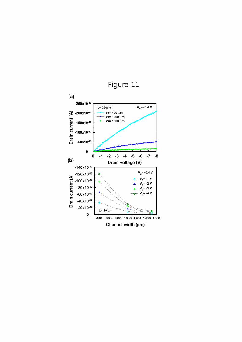
Figure 11
(a)
cu
rren
t (A
)
-250x10-12
-200x10-12
-150x10-12
100 10 12
W= 400 mW= 1000 mW= 1500 m
VG= -0.4 VL= 30 m
-140x10-12
Drain voltage (V)
-8-7-6-5-4-3-2-10
Dra
in c -100x10-12
-50x10-12
0
(b)
Dra
in c
urr
ent
(A) -120x10-12
-100x10-12
-80x10-12
-60x10-12
-40x10-12
-20x10-12
VD= -1 V
VD= -2 V
VD= -3 V
VD= -4 V
VG= -0.4 V
L= 30 m
Channel width (m)
400 600 800 1000 1200 1400 16000
L= 30 m