Embed Size (px)
Citation preview

OpenSerDes: An Open Source Process-PortableAll-Digital Serial Link
Gaurav Kumar K, Baibhab Chatterjee and Shreyas SenSchool of ECE, Purdue University, West Lafayette, USA-47906. email:{gauravk, bchatte, shreyas}@purdue.edu
Abstract—Over the last decade, the growing influence of opensource software has necessitated the need to reduce the abstractionlevels in hardware design. Open source hardware significantlyreduces the development time, increasing the probability of first-pass success and enable developers to optimize software solutionsbased on hardware features, thereby reducing the design costs.The recent introduction of open source Process Development Kit(OpenPDK) by Skywater technologies in June 2020 has eliminatedthe barriers to Application-Specific Integrated Circuit (ASIC)design, which is otherwise considered expensive and not easily ac-cessible. The OpenPDK is the first concrete step towards achievingthe goal of open source circuit blocks that can be imported to reuseand modify in ASIC design. With process technologies scalingdown for better performance, the need for entirely digital designs,which can be synthesized in any standard Automatic Place-and-Route (APR) tool, has increased considerably, for mappingphysical design to the new process technology. This work presentsa first open source all-digital Serializer/Deserializer (SerDes) formulti-GHz serial links designed using Skywater OpenPDK 130nmprocess node. To ensure that the design is fully synthesizable, theSerDes uses CMOS inverter based drivers at the transmitter, whilethe receiver front end comprises a resistive feedback inverter asa sensing element, followed by sampling elements. A fully digitaloversampling CDR at the receiver end recovers the transmitterclock for proper decoding of data bits. The physical design flowutilizes OpenLANE, which is an open source end-to-end tool forgenerating GDS from RTL. Cadence Virtuoso has been used forextracting parasitics for post-layout simulations, which exhibitthe SerDes functionality at 2 Gbps for 34 dB channel loss whileconsuming 438 mW power. The generated GDS and netlist files ofthe SerDes, along with the required documentation, are uploadedin a GitHub repository for public access.
Index Terms—OpenSerdes, Open source, OpenPDK, Skywater
I. INTRODUCTION
A. The Need for open source Hardware
With the predominance of open source software in recenttimes, the term “open source hardware”, introduced by BrucePerens in 1997, is gaining momentum in the design ecosystem[1], [2]. Open source hardware refers to a hardware, an ASIC,or even, a circuit that has provided access to its entire design,specifications, and documentations, which can be used, altered,or distributed by anyone. Like source code in case of opensource software, all the schematics, logic designs, layout-data,and netlists need to be made available for revisions by anyone,who has access to the tools to read, manipulate and updatethe existing design with new features, usually aiming forbetter performance and share the improved design back to thecommunity for further enhancements/evaluations.
Open source hardware reduces the design time, enables soft-ware developers to effectively optimize their source codes based
Scalable
Synthesizable
All-digital
1 RTL Design
2 EDA tools
3 PDK
Prerequisites
ASIC
1 Cost
2 Expertise
3
Risks of failure
Challenges
4
Restricted
access to PDK
Open
Source
ASIC
Solution
1 Zero Licensing fee
2 Automated EDA Open Tools
3
Proven design for sourcing4
Google’s Skywater OpenPDK
ASIC Design: Challenges and Solutions
Need for Digital cores
1970 1980 1990 2000 2010 2020
10µm
1µm
100nm
10nm
Evolution of Process Node
Pro
cess
No
de
Year
1. Easily available
i. Opencores
ii. FPGA
prototype
2. Process portable
Process scalability
for faster time to
market
Digital CoresProblem
SerDes - opencore
- FGPA-based
Goal
OpenSerDes - opensource
- easily portable
Research OutlineOpen Tools
Open PDK
Open source O
P
E
N
S
E
R
D
E
S
Fig. 1. Motivation for open source hardware design and OpenSerDes
on hardware features, accelerates innovations with multiplepeople working together and sharing their knowledge, reducingthe cost. This illustrates the need for open source hardware forfaster technological advancement.
Several Open source hardware projects, like RISC-V [3],UC Berkley’s BAG [4], Google’s OpenTitan [5], OpenRoad[6] etc., have started uploading their design specifics in therepositories for public use. Berkeley Analog Generator (BAG)[7] is an open source tool that provides framework for gen-erating Analog and Mixed Signal (AMS) circuits from thedesign specifications. Numerous Open source tools like magic,ngspice, etc. have been used extensively for design layoutand simulations. The Free and Open Source Silicon (FOSSi)foundation promotes free and open digital hardware designs,supporting open standards development. The recent introduc-tion of Skywater 130 nm open source PDK [1], [8] by Googleand Skywater Foundries, has opened several opportunities forcircuit designers. The conventional PDKs from TSMC, GlobalFoundries, UMC etc. are quite expensive and involve strictlicensing process, making them difficult to access for all.OpenPDK has removed the roadblocks for ASIC designing,providing access to make custom chips for free initially forfaster development cycle or at very low-cost eventually.
With the process technologies scaling down for better per-formance, the existing designs or circuits need to be ported tolatest process, reinstating the fact that “process-portability” ofthe design plays a key role in selecting the circuit topology.Although Analog/Mixed signal circuit design approach mayexhibit superior performance than constituent synthesizabledigital-only circuits, in terms of speed, power, etc., the entiredesign needs to be redrawn from scratch, to port to a new pro-cess. This promotes for synthesizable, digital-friendly designs
arX
iv:2
105.
1325
6v1
[ee
ss.S
Y]
27
May
202
1

that can be easily ported from one process to another.SerDes, an important building block in communication sys-
tems, helps in transmitting a parallel stream of data fromblock to another over serial links, thereby reducing the numberof I/O pins, device dimensions, and power consumption ofthe system. The unavailability of opencore or FPGA-baseddigital IO/SerDes prevents faster time-to-market for designs,as they demand considerable time and effort for porting acrosstechnologies. This work presents the functionality of fully opensource, multi-GHz, all-digital SerDes link, built using Skywater130nm Open PDK, ensuring process-portability, thereby reduc-ing the overhead porting time.
B. Our Contribution
• This work presents the first open source all-digitalSerDes, with multi-GHz capabilities. Unlike traditionalmixed-signal SerDes designs, the all-digital design makesthe present design process-portable, which is a key aspectof Open-Source Hardware.
• This work uses, for the first time, an open source PDK,skywater 130 nm, for the realization of SerDes.
• The work illustrates the importance of open source hard-ware and synthesizable design techniques, motivating theiradoption in circuit design.
C. Paper Organization
The remainder of the paper is organized as follows. SectionII illustrates the importance for open source hardware bycomparing with traditional design techniques. In Section III,the typical architecture of the SerDes link is demonstrated,discussing the various design considerations, while promotingthe need for all-digital design. Section IV presents the archi-tecture of the automated SerDes design. Section V discussesthe implementation results of the SerDes. Section VI explainsthe pros and cons of the design with use-cases and design flowof the OpenLANE tool. We conclude the paper in Section VII.
II. OPEN SOURCE HARDWARE VS. TRADITIONAL DESIGN
Open hardware removes the common hindrances to systemdesign and ensures faster development time. Hardware/ASICdesigners can reduce the risk of design failure by leveragingpre-existing designs in an open source hardware library, whichenables a “plug and play” feature for previously proven success-ful hardware constructs, which was not possible earlier [2]. De-signers possess the complete design that can be modified basedon their required specifications. This prevents re-inventing thedesigns, enables rapid innovation and progress, while loweringthe design cost. Figure 2 shows the comparison between thecosts incurred in manufacturing chip using traditional PDKs(i.e., TSMC, GF, Intel, etc.), and skywater 130nm openPDK.It can be seen that openPDK reduces the PDK licensing cost,bringing down the overall chip manufacturing cost. Note thatthe PDK licensing cost is not publicly accessible and thus, it hasbeen scaled relative to fabrication cost and process technology[9].
The involvement of community facilitates faster evolutionand reception of the design [10]. It enables people to interact
Process Technology (in nm)
2
1
0
Rel
ativ
e C
ost
90 65 45 32 22 14
PDK Licensing Fee
Chip fabrication cost
OpenPDK
Conventional PDKCost for ASIC
Fig. 2. Comparison of Relative chip fabricating cost using Open source PDKand traditional PDKs [9]
and share their knowledge of hardware design, thereby openingmore avenues for innovation. It also provides the softwaredevelopers the ability to optimize and enhance their solutionsbased on the hardware features, impacting the overall perfor-mance of the system. Ultra-low power pervasive IoT, beingat the juncture of Moore’s Law and Shannon’s law, calls forinnovation and collaboration at both software and hardwarefronts [11], and hence would benefit immensely from open-source hardware designs.
Open source hardware has started to gain prominence in thedesign space, with numerous open source projects, like BAG,RISC-V, OpenTitan, OpenPDKs etc., promoting open standarddevelopments. In a nutshell, open source hardware providespeople with a platform to share their knowledge and determinethe course of the technology.
III. SERDES DESIGN CONSIDERATIONS
SerDes has emerged as a popular solution in communicationsystem design since the paradigm shift away from traditionalparallel communication standards to overcome the voltagescaling dependencies and performance limitations. Serial links,unlike parallel implementations, are scalable and require fewerI/Os, achieve smaller device footprints, thereby having lowerpower requirements.The growing demand for low-power high-speed link has motivated development of innovative circuittechniques for SerDes over the last few years [12]–[14]. Mixed-signal designs, having multiple feedback loops from analogand digital domains, have presented a cost-effective solution,reaping the benefits of both analog and digital worlds. Butwith consequent technology scaling, requiring faster time-to-market for lower process node designs, there is a need for all-digital SerDes architecture, which can be easily ported acrosstechnologies.
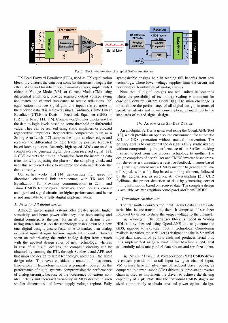
Figure 3 shows the block-level architecture of a typicalSerDes. The transmitter (TX) front end comprises of a seri-alizer, TX equalization block and a driver, while the Receiver(RX) front end has RX equalization, sampling element and adeserializer [15]. In case of non-forwarded-clock architecture,where timing signal of the transmitter, i.e. clock, is not trans-mitted along with data, a Clock and Data Recovery (CDR)circuit recovers the timing information and facilitates correctdecoding of received data.
OSC
Sampler/
Comparator
CDR
DeS
erializerCL
K
32
32
32
32
32
32
Serializer
Transmitter
Equalization
FP
GA
CL
K
32
32
32
32
32
32
Transmitter
FFERX FIR/CTLE/
DFE/VGA
CL
K
FP
GA
CM/VM
Driver
Receiver
Serial Link
CMOS Inverter
SA/ CML
Receiver
Equalization
Fig. 3. Block-level overview of a typical SerDes Architecture
TX Feed Forward Equalizer (FFE), used as TX equalizationblock, pre-distorts the data over some bit durations to negate theeffect of channel loss/distortion. Transmit drivers, implementedeither in Voltage Mode (VM) or Current Mode (CM) usingdifferential amplifiers, provide required output voltage swingand match the channel impedance to reduce reflections. RXequalization improves signal gain and input referred noise ofthe received data. It is achieved using a Continuous Time LinearEqualizer (CTLE), a Decision Feedback Equalizer (DFE) orFIR filter based FFE [16]. Comparator/Sampler blocks resolvethe data to logic levels based on some threshold or differentialvalue. They can be realized using static amplifiers or clockedregenerative amplifiers. Regenerative comparators, such as aStrong Arm Latch [17] samples the input at clock edges andresolves the differential to logic levels by positive feedbackbased latching action. Recently, high speed ADCs are used ascomparators to generate digital data from received signal [18].A CDR extracts the timing information from the incoming datatransitions, by adjusting the phase of the sampling clock, anduses this recovered clock to resample the data and decode thedata correctly.
Our earlier works [13] [14] demonstrate high speed bi-directional electrical link architecture, with TX and RXEqualization, for Proximity communication in 22nm and14nm CMOS technologies. However, these designs consistanalog/mixed-signal circuits for higher performance, and henceis not amenable to a fully digital implementation.
A. Need for All-digital design
Although mixed signal systems offer greater speeds, highersensitivity, and better power efficiency than both analog anddigital counterparts, the push for an all-digital design is gar-nering much interest. As the technology scales down to a newone, digital designs ensure faster time to market than analogor mixed signal designs because significant amount of time isspent on refabricating the entire analog design from scratchwith the updated design rules of new technology, whereasin case of all-digital designs, the complete circuitry can beobtained by running the RTL through Synthesis and APR toolthat maps the design to latest technology, abiding all the latestdesign rules. This saves considerable amount of man-hours.Innovations in technology scaling is primarily focused on theperformance of digital systems, compromising the performanceof analog circuitry, because of the occurrence of various non-ideal effects and increased variability in MOS device, in suchsmaller dimensions and lower supply voltage regime. Fully
synthesizable designs help in reaping full benefits from newtechnology, where lower voltage supplies limit the circuit andperformance feasibilities of analog circuits.
Note that all-digital designs are well suited in scenarioswhere the possibility of technology scaling is imminent (incase of Skywater 130 nm OpenPDK). The main challenge isto maximize the performance of all-digital design, in terms ofspeed, sensitivity and power consumption, to match up to thestandards of mixed signal design.
IV. AUTOMATED SERDES DESIGN
An all-digital SerDes is generated using the OpenLANE Tool[19], which provides an open source environment for automaticRTL to GDS generation without manual intervention. Theprimary goal is to ensure that the design is fully synthesizable,without compromising the performance of the SerDes, makingit easier to port from one process technology to another. Thedesign comprises of a serializer and CMOS inverter based trans-mit driver as a transmitter, a resistive-feedback inverter-based[20] sensing element and a CMOS inverter to generate rail-to-rail signal, with a flip-flop-based sampling element, followedby the deserializer, as receiver. An oversampling [21] CDRfacilitates the proper detection of data by generating correcttiming information based on received data. The complete designis available at: https://github.com/SparcLab/OpenSERDES.
A. Transmitter Architecture
The transmitter converts the input parallel data streams intoserial bits, before transmitting them. It comprises of serializerfollowed by driver to drive the output voltage to the channel.
a) Serializer: The Serializer block is coded in VerilogHDL and synthesized using OpenLANE tool to generate theGDS, mapped to Skywater 130nm technology. Consideringrealistic scenarios, the serializer is designed to take in 8 parallelinput data streams of 32 bits each and produces serial bits.It is implemented using a Finite State Machine (FSM) thatsequentially takes one parallel data stream and serializes them.
b) Transmit Driver: A voltage-Mode (VM) CMOS driveris chosen provide rail-to-rail input swing at channel input.VM drivers have an advantage of reduced driver power, ascompared to current-mode (CM) drivers. A three-stage inverterchain is used to implement the driver, to achieve the drivingcapability of 2 pF. Note that the individual CMOS stages aresized appropriately to obtain area and power optimal design.

30 32 34 36 38 40 42 44 46 48 50Time (in ns)
0
0.5
1
1.5
2
30 32 34 36 38 40 42 44 46 48 50Time (in ns)
0
0.5
1
1.5
2
Inp
ut
Ou
tpu
t
2 pF
OutputInput
(a) (b)
ZL
Inverter-based VM Driver
Size Increases
Fig. 4. (a) Schematic of CMOS Transmit Driver (b) Input/Output Waveformsof Driver at 2 Gbps with 2 pF termination
Figure 4 shows the schematic representation of designed CMOSinverter-based driver, with related input-output waveforms.
B. Receiver Architecture
The receiver front end uses a resistive feedback inverter asgain and sensing element and a CMOS inverter based staticcomparator for sampling the received signal. These blocks arechosen to ensure that the SerDes receiver is synthesizable andachieves desired performance criteria. Figure 5 presents thecomplete receiver architecture of the SerDes.
DFF CDR
EXT CLK
Static
CMOS
inverter
Oversampling CDR
Sampling Stage
FSMSerial to
Parallel
DeS
erializer
32
32
32
32
32
32
32
Resistive Feedback
CMOS Inverter
Sensing Stage
Pseudo-resistor
Off-Chip
Coupling Cap
IN
Fig. 5. Receiver architecture of presented SerDes
a) Resistive Feedback Inverter: The Resistive feedbackinverter [20] is a self-biased CMOS inverter with a resistivefeedback from output to input, aiming to bias the inverter nearthe switching threshold, i.e. 0.5VDD point, enabling the CMOSinverter to work on signals with amplitudes much lower thanits threshold voltage. To ensure synthesizability, the feedbackresistor is realized as pseudo resistor using PMOS, where thegate and source are shorted to operate in linear resistive region.An off-chip capacitor is used to AC couple the received signaland prevent the received signal to interfere with the generatedself-bias voltage, thereby maintaining the DC bias. Since theinverter operates at the point where both PMOS and NMOS arein saturation, there always exists a path for current to flow fromsupply to ground, resulting in non-zero static power disspiation.Figure 6 shows the operating point of the designed self-biasinverter, with waveforms depicting its functionality.
b) Sampling Block: The sampling block consists ofCMOS inverter, which provides rail-to-rail signal at the inputof D flip-flop, which then samples and forwards the receiveddata to the deserializer, using the timing information providedby clock signal. Although the realized sampling topology haslimited gain as compared to regenerative samplers/comparators,the front-end resistive feedback inverter compensates and pro-vides the necessary gain.
0 1.8
1.8
0Input (in V)
Ou
tpu
t (i
n V
)
DC Bias = 0.83 V
DC characteristics
30 32 34 36 38 40 42 44 46 48 50Time (in ns)
0
0.02
0.04
30 32 34 36 38 40 42 44 46 48 50Time (in ns)
0.82
0.84
0.86
30 32 34 36 38 40 42 44 46 48 50Time (in ns)
0.7
0.8
0.9
1
Inp
ut
Bia
sed
Inp
ut
Ou
tpu
t
32 mV
300 mV
Biased
around
835mV
Input from
ChannelOutput to
inverter
Fig. 6. (a) Operating point, (b) Input/Output Waveforms, of Resistive feedbackinverter
c) Deserializer: The deserializer block converts serial bitsinto parallel data streams, which are to be interfaced with otherblocks. It is implemented through an FSM that takes in serialbits and produces 8 parallel data streams of 32 bits each atthe end of its operation. The entire design is synthesized usingOpenLANE tool to generate the GDS and netlists.
C. Oversampling CDR
A fully digital oversampling CDR [21] [22] is implementedto recover the clocking information. It samples the received dataat multiple points, stores them in FIFO registers, before deter-mining the optimal sampling point, which is used to correctlydetermine the transmitted data. The CDR is also equipped withtunable glitch and jitter correction logic using external scan bits.An external clock is fed to the phase generator block to producemultiple clock phases needed for sampling the input at differentpoints. The sampled data is sent for processing and decision-making, using the predefined logic of the decision block andexternal glitch and jitter corrections inputs. Figure 7 shows theblock-level architecture of implemented Oversampling CDR.
Register
Bank
Bit
Bo
un
dary
detectio
n
Decision
Block
Recovered Data Bit
DATA
PROCESSING
& DECISION
BLOCK
Glitch Correction ScanJitter Correction Scan
Multiphase
Clock
Generator
Multiple
phase
Samplers
CLOCKING BLOCK
SAMPLING BLOCK
Input
Clock
Data
Input
Fig. 7. Architecture of implemented Oversampling CDR
V. RESULTS
The SerDes design (in GDSII format) is imported in ca-dence virtuoso to extract parasitics and perform post-layoutsimulations. Figure 8 shows the input/output waveforms ofSerDes link at 2 GHz with PRBS-31 input. The received signalrepresents the signal reaching the RX front end, after channelattenuation of 34 dB. In contrast with Strong-Arm Latch [17]based receiver designs, which are sensitive to even 10 mVsignals at 2 GHz, the presented all-digital design achieves ≈ 32mV sensitivity, which is promising in several applications likePCIe interfaces, short-range interconnects, where the requiredbandwidths are less and channel losses are not significant.

30 40 50 60 70 80 90 100Time (in ns)
0
1
2
30 40 50 60 70 80 90 100Time (in ns)
0
0.02
0.04
30 40 50 60 70 80 90 100Time (in ns)
0
1
2
Tra
nsm
itte
dR
ecei
ved
Dec
od
ed
32mV
Fig. 8. Input/Output Wave-forms at 2Gbps for the SerDes link.
The variation of sensitivity of SerDes receiver with differentoperating frequencies is depicted in Figure 9. Note that themaximum channel loss corresponding to zero BER transmissionis also shown.
1M 10M 100M 1G
Frequency (Hz)
15
20
25
30
35
Se
ns
itiv
ity
(m
V)
-50
-45
-40
-35
Max. C
han
nel L
oss (
dB
)
Fig. 9. Variation of Sensitivity and maximum operating channel loss of SerDesReceiver with frequency of operation
RX Front End1
10
100
1000
10000
100000
1000000
Area BreakdownPower Budget
4.5 mW6.7 mW
1.4 mW3.1 mW
CMOS
Driver
RX FE
CDR
Serializer
De-Serializer
Are
a (𝒖𝒎𝟐)
CMOS driver
Resistive Feedback Inverter
Static CMOS Inverter
D Flipflop
Fig. 10. Power Budget and Area Breakdown of the designed Serial link.
Figure 10 provides the power consumption (excluding se-rializer, deserializer and CDR blocks) and area of the all-digital serial link. The link needs total power of 15.7 mWoperating at 2 GHz for the supply of 1.8V, with the receiverand transmitter consuming 11.2 mW, and 4.5 mW respectively.Serializer, Deserializer and CDR circuits require additional235mW, 128mW and 59mW respectively. The high powernumbers of serializer and deserializer blocks are the resultof intended design choices to support large IO streams (eightparallel links with 32-bit input) for communication. Thus, theimplemented all-digital SerDes operates at 2 GHz for 34 dBchannel loss, while consuming power of 437.7 mW, therby
exhibiting energy efficiency of 219 pJ/bit. Figure 11 presentsthe layout of the design. The design layout extends over anarea of 0.24mm2, with deserializer occupying 60% of the area,while the CMOS driver and RX Front end cover 0.2% and 1.1%respectively.
CDR
Deserializer
SerializerRX Front
End
CMOS Driver
Fig. 11. Layout of the generated SerDes. The complete design is available at:https://github.com/SparcLab/OpenSERDES
VI. DISCUSSIONS
a) Pros and Cons of the presented SerDes design: TheSerDes is equipped with the capability to support multi-GHztransmission, in addition to being a fully synthesizable design,ensuring process-portability. Except for serializer, deserializerand CDR, the entire serial link is implemented using a fewCMOS inverters and MOS devices, thereby requiring less chiparea compared to mixed signal circuit design, which requireadditional complex circuitry and I/O pins to provide appropriatebiasing for functioning.
However, compared to conventional mixed signal circuitapproach, the presented SerDes exhibits slightly lesser sensi-tivity, and operates at lower speeds, making it appropriate forapplications, where the required operating speeds are smaller(1-2 GHz), channel losses are moderate (34dB - 40dB).
b) Applications: The generated SerDes can be used tointerface links where the bandwidth requirements is < 2 Gbps,like the PCIe 1.x, PCIe 2.x, PCIe 3.x, PCIe 4.0 bus, where therequired Bandwidth/lane ranges from 250 Mbps to 2 Gbps. TheSerDes can also find applications in high bandwidth density,short-range interconnects between chiplets, like Intel’s recenthigh density, multi-die packaging paradigm, Embedded Multi-die interconnects (EMIB) [23],where the primary focus is onthe area of the serial link, requiring data speeds in the range of1-4 GHz in a significantly low channel loss setting of 1-5 dB.
c) OpenLANE Tool flow: The OpenLANE tool [19], anopen source tool with automated RTL to GDS flow, is used tosynthesize the RTL and generate GDS for the SerDes design.The OpenLANE tool flow uses custom methodology scriptsthat perform design exploration and optimization and chose thebest implementation, using a number of constituent open sourcetools, like magic, yosys, OpenSTA, etc., which are invokedat different times in the flow, to execute the Synthesis, APR,Verification and Export steps of the ASIC design flow. Figure

RTL
Synthesis
yosys + abc
Timing
Analysis
OpenSTA
Timing Violation Found
Optimization
Global Routing
OpenROAD App
SYNTHESIS
Floor Planning
Placement
Clock Tree Syn
Desig
n E
xplo
ration
AUTOMATIC
PLACE &
ROUTE
VERIFICATION
+ EXPORT
LEC
yosys
Detailed
Routing
TritonRoute
Timing
Analysis
OpenSTA
GDS
export
magic
Physical
Verification
magic + netgen
Block
Functionality
Open Tools Used
Source RTLGDS
Fig. 12. Design Flow of OpenLANE tool
12 shows the overview of OpenLANE tool flow, also indicatingthe open source tools used in each step of the flow.
VII. CONCLUSION
The common roadblocks to hardware/ASIC designs, i.e.,the high commitment costs, the much-needed expertise of thedesigner and the uncertainty (risk) of design functionality,prevent the designers from the required access to advancedtechnologies. With main objective to democratize the hardwaredesign, the open source hardware revolution is gaining interest,with several open source EDA tools and designs are begin-ning to surface for public use. These designs and tools canbe sourced, modified, or enhanced by the designers, therebyeliminating the involved design cost and the risk factors. Thetools are incorporated with machine learning and optimizationcapabilities, with automated flow, that generate the fully op-timized implementation of complex designs. This significantlybrings down the applied human effort, and removes the level ofneeded expertise through automated open source popular EDAtools such as magic, ngspice, OpenRoad, OpenLANE, BAGetc. The advent of open source PDK by Google and Skywatertechnologies has provided designers with free access to theCMOS 130 nm process, equipping them with standard libraryneeded for generating designs. Thus, Open source hardwaresignificantly reduces the development time and costs for thedesign. Technology scaling is also shifting the focus to digital-only designs as analog circuits suffer from short channel effectsand degraded performance at low voltage supplies. All-Digitalor synthesizable designs also enable faster time-to-market thananalog designs.With the development of APR tools, the all-digital designs can be easily ported to new process with mini-mal effort. Consequently, all-digital designs are being preferredtoday over analog or mixed signal designs.
The work presents the first open source SerDes using Skywa-ter 130 nm OpenPDK, aiming to build a synthesizable design,ensuring process-portability, without compromising with theperformance of the design. Simulation results show that thedesigned SerDes operates at speed of 2 GHz, has a receiversensitivity of 32 mV to cope up with the channel losses of 34dB, while consuming power of 438 mW. The generated SerDesfinds applications in interfaces, where the required data rates arenot very high, for example in PCIe bus interfaces and in short-reach interconnects between chiplets. The data speed and poweris primarily limited by the Skywater 130 nm, the only Open
PDK available presently, and will improve significantly as newOpenPDK’s are made available. The presented work signifiesthe beginning of the open source ASIC designing, especiallyin traditionally mixed-signal-heavy circuits such as the SerDes,and may serve as a guide to prospective hardware/ASIC design-ers, illustrating the importance of open source hardware, andmotivating them towards digital-friendly designs using opensource tools and PDK.
ACKNOWLEDGMENT
This work was supported in part by the SemiconductorResearch Corporation (SRC) CHIRP Program, under Grant No.2878.014 and the National Science Foundation (NSF) CareerAward under Grant No. ECCS 1944602. The authors wouldlike to thank Nirmoy Modak and Debayan Das, Ph.D. studentsat Purdue University for their valuable feedback during writingthe manuscript.
REFERENCES
[1] P. Wagner. “Produce your own physical chips. For free. Inthe Open.”, [Online]. Available:https://fossi-foundation.org/2020/06/30/skywater-pdk, June, 2020.
[2] C. Tozzi. “Open Source Hardware: What It Means and Why It Mat-ters”, [Online]. Available:https://www.channelfutures.com/open-source/open-source-hardware-what-it-means-and-why-it-matters, 2016.
[3] “RISC-V”, [Online]. Available:https://github.com/riscv.[4] “Berkeley analog generator, main framework”, [Online]. Available:https:
//github.com/ucb-art/BAG framework.[5] “OpenTitan”, [Online]. Available:https://github.com/lowRISC/opentitan.[6] “The-OpenROAD-Project”, [Online]. Available:https://github.com/
The-OpenROAD-Project.[7] E. Chang et al. “BAG2: A process-portable framework for generator-
based AMS circuit design”. In 2018 CICC, pages 1–8, 2018.[8] “Skywater”, [Online]. Available:https://github.com/google/skywater-pdk.[9] B. Holt. “Advancing Moore’s Law”, [Online]. Available:
https://www.intel.com/content/www/us/en/silicon-innovations/advancing-moores-law-in-2014-presentation.html, 2015.
[10] V. Tigadi. “Take advantage of open-source hardware”. Available:https://www.edn.com/take-advantage-of-open-source-hardware/, 2016.
[11] B. Chatterjee, N. Cao, A. Raychowdhury, and S. Sen. “Context-Aware Intelligence in Resource-Constrained IoT Nodes: Opportunitiesand Challenges”. IEEE Design & Test, 36(2):7–40, 2019.
[12] B. Razavi. “Historical Trends in Wireline Communications: 60? Im-provement in Speed in 20 Years”. IEEE Solid-State Circuits Magazine,7(4):42–46, 2015.
[13] T. Musah et al. “A 4–32 Gb/s Bidirectional Link With 3-Tap FFE/6-TapDFE and Collaborative CDR in 22 nm CMOS”. JSSC, 2014.
[14] C. Thakkar et al. “A 32 Gb/s Bidirectional 4-channel 4 pJ/b CapacitivelyCoupled Link in 14 nm CMOS for Proximity Communication”. JSSC,2016.
[15] W. J. Dally and J. W. Poulton. Digital Systems Engineering. CambridgeUniversity Press, USA, 1st edition, 2008.
[16] B. Razavi. RF Microelectronics (2nd Edition). Prentice Hall Press, USA,2nd edition, 2011.
[17] B. Razavi. “The StrongARM Latch [A Circuit for All Seasons]”. IEEESolid-State Circuits Magazine, 7(2):12–17, 2015.
[18] J. Im et al. “6.1 A 112Gb/s PAM-4 Long-Reach Wireline TransceiverUsing a 36-Way Time-Interleaved SAR-ADC and Inverter-Based RXAnalog Front-End in 7nm FinFET”. In 2020 ISSCC, pages 116–118,2020.
[19] “OpenLANE”, [Online]. Available:https://github.com/efabless/openlane.[20] B. Woorham. “CMOS Inverter as Analog Circuit: An Overview”. In
Journal of Low Power Electronics and Applications, volume 9, page 3:26,2019.
[21] S. I. Ahmed and T. A. Kwasniewski. “Overview of oversampling clockand data recovery circuits”. In Canadian Conference on Electrical andComputer Engineering, 2005., pages 1876–1881, 2005.

[22] C. Hung, M. Chiang, A. Lee, and S. Lee. “A Sub-1V CMOS 2.5Gb/sSerial Link Transceiver Using 2X Oversampling”. In 2005 IEEE AsianSolid-State Circuits Conference, pages 37–40, 2005.
[23] R. Mahajan et al. “Embedded Multi-die Interconnect Bridge (EMIB) – AHigh Density, High Bandwidth Packaging Interconnect”. In 2016 ECTC,pages 557–565, 2016.