Embed Size (px)
Citation preview
1SLOU474–June 2017Submit Documentation Feedback
Copyright © 2017, Texas Instruments Incorporated
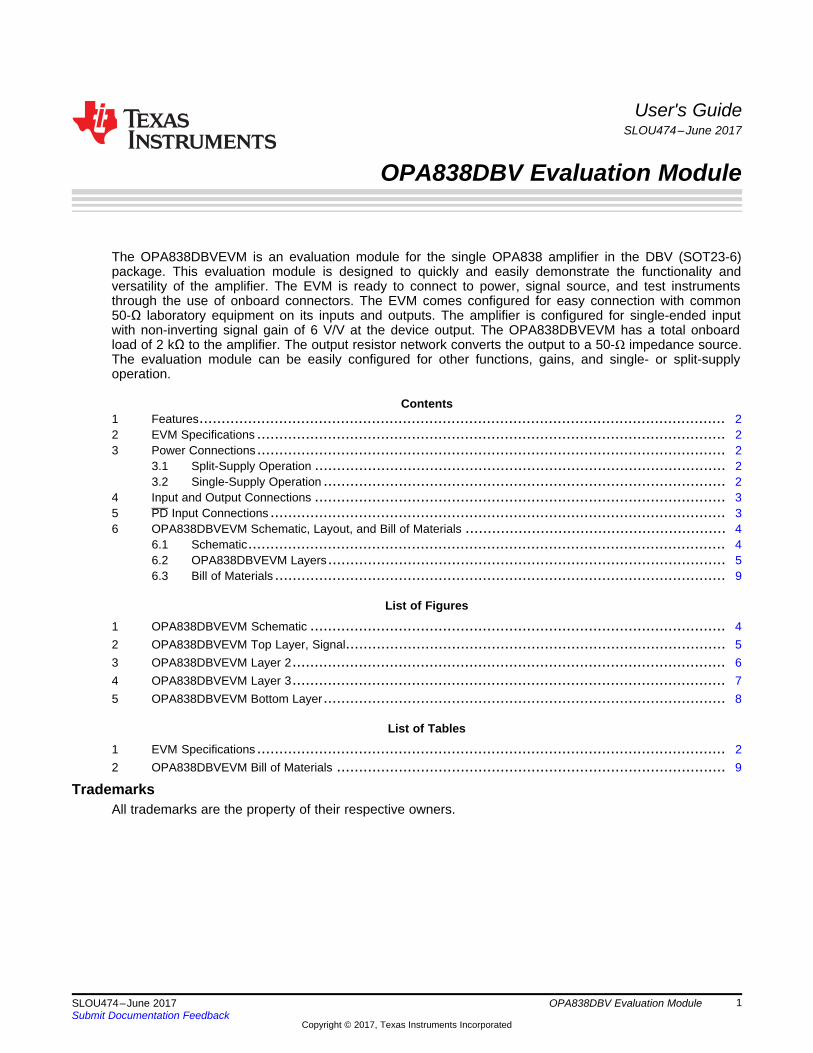
OPA838DBV Evaluation Module
User's GuideSLOU474–June 2017
OPA838DBV Evaluation Module
The OPA838DBVEVM is an evaluation module for the single OPA838 amplifier in the DBV (SOT23-6)package. This evaluation module is designed to quickly and easily demonstrate the functionality andversatility of the amplifier. The EVM is ready to connect to power, signal source, and test instrumentsthrough the use of onboard connectors. The EVM comes configured for easy connection with common50-Ω laboratory equipment on its inputs and outputs. The amplifier is configured for single-ended inputwith non-inverting signal gain of 6 V/V at the device output. The OPA838DBVEVM has a total onboardload of 2 kΩ to the amplifier. The output resistor network converts the output to a 50-Ω impedance source.The evaluation module can be easily configured for other functions, gains, and single- or split-supplyoperation.
Contents1 Features....................................................................................................................... 22 EVM Specifications .......................................................................................................... 23 Power Connections.......................................................................................................... 2
3.1 Split-Supply Operation ............................................................................................. 23.2 Single-Supply Operation ........................................................................................... 2
4 Input and Output Connections ............................................................................................. 35 PD Input Connections ....................................................................................................... 36 OPA838DBVEVM Schematic, Layout, and Bill of Materials ........................................................... 4
6.1 Schematic............................................................................................................ 46.2 OPA838DBVEVM Layers.......................................................................................... 56.3 Bill of Materials ...................................................................................................... 9
List of Figures
1 OPA838DBVEVM Schematic .............................................................................................. 42 OPA838DBVEVM Top Layer, Signal...................................................................................... 53 OPA838DBVEVM Layer 2.................................................................................................. 64 OPA838DBVEVM Layer 3.................................................................................................. 75 OPA838DBVEVM Bottom Layer........................................................................................... 8
List of Tables
1 EVM Specifications .......................................................................................................... 22 OPA838DBVEVM Bill of Materials ........................................................................................ 9
TrademarksAll trademarks are the property of their respective owners.
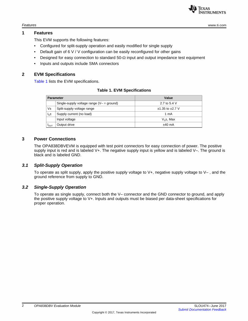
Features www.ti.com
2 SLOU474–June 2017Submit Documentation Feedback
Copyright © 2017, Texas Instruments Incorporated
OPA838DBV Evaluation Module
1 FeaturesThis EVM supports the following features:• Configured for split-supply operation and easily modified for single supply• Default gain of 6 V / V configuration can be easily reconfigured for other gains• Designed for easy connection to standard 50-Ω input and output impedance test equipment• Inputs and outputs include SMA connectors
2 EVM SpecificationsTable 1 lists the EVM specifications.
Table 1. EVM Specifications
Parameter ValueSingle-supply voltage range (V– = ground) 2.7 to 5.4 V
V± Split-supply voltage range ±1.35 to ±2.7 VIS± Supply current (no load) 1 mA
Input voltage VS±, MaxIOUT Output drive ±40 mA
3 Power ConnectionsThe OPA838DBVEVM is equipped with test point connectors for easy connection of power. The positivesupply input is red and is labeled V+. The negative supply input is yellow and is labeled V–. The ground isblack and is labeled GND.
3.1 Split-Supply OperationTo operate as split supply, apply the positive supply voltage to V+, negative supply voltage to V– , and theground reference from supply to GND.
3.2 Single-Supply OperationTo operate as single supply, connect both the V– connector and the GND connector to ground, and applythe positive supply voltage to V+. Inputs and outputs must be biased per data-sheet specifications forproper operation.

www.ti.com Input and Output Connections
3SLOU474–June 2017Submit Documentation Feedback
Copyright © 2017, Texas Instruments Incorporated
OPA838DBV Evaluation Module
4 Input and Output ConnectionsThe OPA838DBVEVM is equipped with SMA connectors for easy connection of signal generators andanalysis equipment. As shipped, the EVM is configured for a non-inverting gain of 6 V/V, split supplyoperation, single-ended input and output with 50-Ω termination. For best results, signals must be routed toand from the EVM with cables having 50-Ω characteristic impedance. IN+ (J2) should be used for single-ended input with 50-Ω source. OUT (J5) is the output connector. A resistor network (R7, R8 and R9) atthe output of the amplifier convert the output signal to 50-Ω single-ended source, and provides a 2-kΩ loadto the amplifier when terminated with 50-Ω load at J5. A 50-Ω line-impedance match at OUT (J5) shouldbe preserved. This results in an output measurement loss, and the overall attenuation is approximately38 dB. See the OPA838 data sheet (SBOS867) applications section, schematics, and layouts for moredetail and how to reconfigure the EVM.
5 PD Input ConnectionsThe PD jumper (J4) allows the OPA838 to be disabled. An SMA connector can also be loaded at J3 and asignal for the power down function can be applied for high-speed testing. Normally the J4 jumper is usedto enable or disable (power down) the amplifier. When jumper J4 is connected to Vs+ using a shortingblock, the amplifier is enabled and when connected to Vs-, the amplifier is disabled. The PD pin shouldnever be left floating.
For high-speed testing, the R12 can be replaced with 50-Ω to terminate the PD SMA input. The shortingblock should be removed from J4 during high-speed testing. 50-Ω at R12 terminates to the ground and notto the supplies. The state of the amplifier will be undefined when the signal source is disconnected. Forthis reason, 50-Ω at R12 should only be used when driving the SMA connector with a high speed,controlled impedance source.

0.01µFC4
GNDGND
0.01µFC6
GND GND
Vs-Vs+
10µFC3
10µFC5
1
2
3
J4PD
TP3GND
GND
TP1V+
TP2V-
0
R11
0
R10
4
3
2
1
65
V+
V-
U1OPA838IDBV
Vs+
1.00k
R6
GND
Vs-
GND
50R4
GND
0R1
0
R5
200
R2
1.96k
R7
51.1R9
GND
2pFC2DNP
GND
0
R8
SH-J4_1-2
Vs+
1.00kR13
Vs-
1.00kR1450
R12DNP
GND
GND
GND
Vs+
Vs-
For recommended operating voltage refer Datasheet/EVM User's Guide
PD
PD
1
2 3 4 5
J2IN+
1
2 3 4 5
J1IN-
1
2345
J5OUT
Note: Pinout for a 6 pin device is shown above.If 5 pin device is used pinout is shown below.
V+
V-
4
3
2
1
5
C7
DNP
0
R15
0
R3DNP
C1
DNP
R16DNP
1
2 3 4 5
J3PD
DNP
GND
Copyright © 2017, Texas Instruments Incorporated
OPA838DBVEVM Schematic, Layout, and Bill of Materials www.ti.com
4 SLOU474–June 2017Submit Documentation Feedback
Copyright © 2017, Texas Instruments Incorporated
OPA838DBV Evaluation Module
6 OPA838DBVEVM Schematic, Layout, and Bill of Materials
6.1 SchematicFigure 1 illustrates the EVM schematic.
Figure 1. OPA838DBVEVM Schematic
www.ti.com OPA838DBVEVM Schematic, Layout, and Bill of Materials
5SLOU474–June 2017Submit Documentation Feedback
Copyright © 2017, Texas Instruments Incorporated
OPA838DBV Evaluation Module
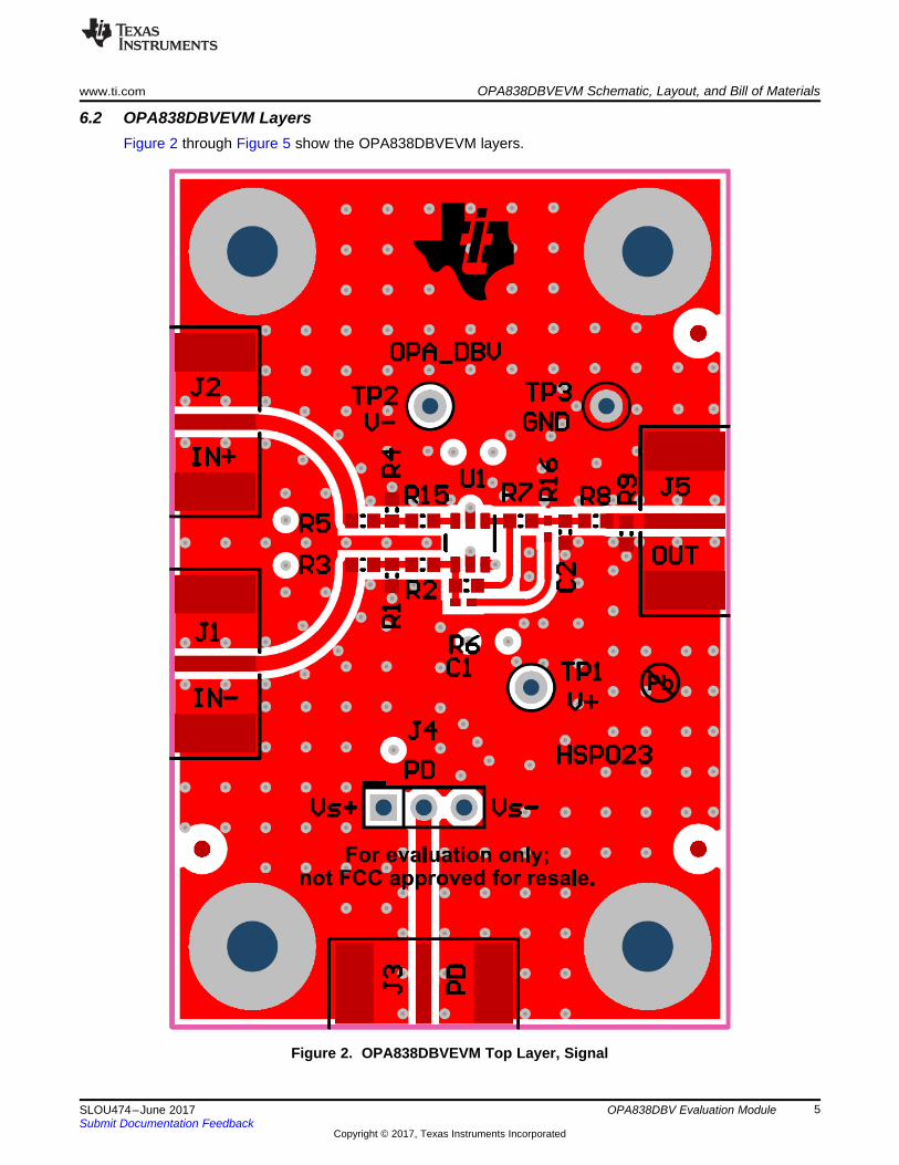
6.2 OPA838DBVEVM LayersFigure 2 through Figure 5 show the OPA838DBVEVM layers.
Figure 2. OPA838DBVEVM Top Layer, Signal

OPA838DBVEVM Schematic, Layout, and Bill of Materials www.ti.com
6 SLOU474–June 2017Submit Documentation Feedback
Copyright © 2017, Texas Instruments Incorporated
OPA838DBV Evaluation Module
Figure 3. OPA838DBVEVM Layer 2

www.ti.com OPA838DBVEVM Schematic, Layout, and Bill of Materials
7SLOU474–June 2017Submit Documentation Feedback
Copyright © 2017, Texas Instruments Incorporated
OPA838DBV Evaluation Module
Figure 4. OPA838DBVEVM Layer 3

OPA838DBVEVM Schematic, Layout, and Bill of Materials www.ti.com
8 SLOU474–June 2017Submit Documentation Feedback
Copyright © 2017, Texas Instruments Incorporated
OPA838DBV Evaluation Module
Figure 5. OPA838DBVEVM Bottom Layer
www.ti.com OPA838DBVEVM Schematic, Layout, and Bill of Materials
9SLOU474–June 2017Submit Documentation Feedback
Copyright © 2017, Texas Instruments Incorporated
OPA838DBV Evaluation Module
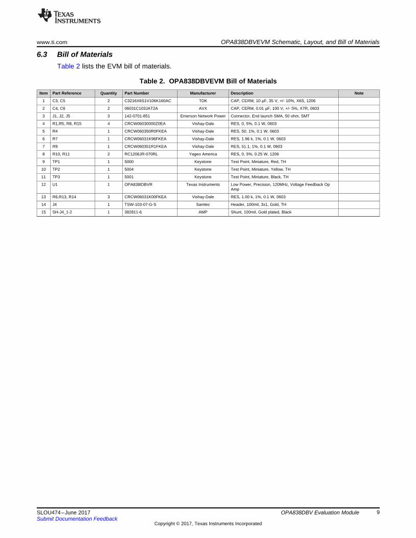
6.3 Bill of MaterialsTable 2 lists the EVM bill of materials.
Table 2. OPA838DBVEVM Bill of MaterialsItem Part Reference Quantity Part Number Manufacturer Description Note
1 C3, C5 2 C3216X6S1V106K160AC TDK CAP, CERM, 10 µF, 35 V, +/- 10%, X6S, 1206
2 C4, C6 2 06031C103JAT2A AVX CAP, CERM, 0.01 µF, 100 V, +/- 5%, X7R, 0603
3 J1, J2, J5 3 142-0701-851 Emerson Network Power Connector, End launch SMA, 50 ohm, SMT
4 R1,R5, R8, R15 4 CRCW06030000Z0EA Vishay-Dale RES, 0, 5%, 0.1 W, 0603
5 R4 1 CRCW060350R0FKEA Vishay-Dale RES, 50, 1%, 0.1 W, 0603
6 R7 1 CRCW06031K96FKEA Vishay-Dale RES, 1.96 k, 1%, 0.1 W, 0603
7 R9 1 CRCW060351R1FKEA Vishay-Dale RES, 51.1, 1%, 0.1 W, 0603
8 R10, R11 2 RC1206JR-070RL Yageo America RES, 0, 5%, 0.25 W, 1206
9 TP1 1 5000 Keystone Test Point, Miniature, Red, TH
10 TP2 1 5004 Keystone Test Point, Miniature, Yellow, TH
11 TP3 1 5001 Keystone Test Point, Miniature, Black, TH
12 U1 1 OPA838IDBVR Texas Instruments Low Power, Precision, 120MHz, Voltage Feedback OpAmp
13 R6,R13, R14 3 CRCW06031K00FKEA Vishay-Dale RES, 1.00 k, 1%, 0.1 W, 0603
14 J4 1 TSW-103-07-G-S Samtec Header, 100mil, 3x1, Gold, TH
15 SH-J4_1-2 1 382811-6 AMP Shunt, 100mil, Gold plated, Black

STANDARD TERMS FOR EVALUATION MODULES1. Delivery: TI delivers TI evaluation boards, kits, or modules, including any accompanying demonstration software, components, and/or
documentation which may be provided together or separately (collectively, an “EVM” or “EVMs”) to the User (“User”) in accordancewith the terms set forth herein. User's acceptance of the EVM is expressly subject to the following terms.1.1 EVMs are intended solely for product or software developers for use in a research and development setting to facilitate feasibility
evaluation, experimentation, or scientific analysis of TI semiconductors products. EVMs have no direct function and are notfinished products. EVMs shall not be directly or indirectly assembled as a part or subassembly in any finished product. Forclarification, any software or software tools provided with the EVM (“Software”) shall not be subject to the terms and conditionsset forth herein but rather shall be subject to the applicable terms that accompany such Software
1.2 EVMs are not intended for consumer or household use. EVMs may not be sold, sublicensed, leased, rented, loaned, assigned,or otherwise distributed for commercial purposes by Users, in whole or in part, or used in any finished product or productionsystem.
2 Limited Warranty and Related Remedies/Disclaimers:2.1 These terms do not apply to Software. The warranty, if any, for Software is covered in the applicable Software License
Agreement.2.2 TI warrants that the TI EVM will conform to TI's published specifications for ninety (90) days after the date TI delivers such EVM
to User. Notwithstanding the foregoing, TI shall not be liable for a nonconforming EVM if (a) the nonconformity was caused byneglect, misuse or mistreatment by an entity other than TI, including improper installation or testing, or for any EVMs that havebeen altered or modified in any way by an entity other than TI, (b) the nonconformity resulted from User's design, specificationsor instructions for such EVMs or improper system design, or (c) User has not paid on time. Testing and other quality controltechniques are used to the extent TI deems necessary. TI does not test all parameters of each EVM.User's claims against TI under this Section 2 are void if User fails to notify TI of any apparent defects in the EVMs within ten (10)business days after delivery, or of any hidden defects with ten (10) business days after the defect has been detected.
2.3 TI's sole liability shall be at its option to repair or replace EVMs that fail to conform to the warranty set forth above, or creditUser's account for such EVM. TI's liability under this warranty shall be limited to EVMs that are returned during the warrantyperiod to the address designated by TI and that are determined by TI not to conform to such warranty. If TI elects to repair orreplace such EVM, TI shall have a reasonable time to repair such EVM or provide replacements. Repaired EVMs shall bewarranted for the remainder of the original warranty period. Replaced EVMs shall be warranted for a new full ninety (90) daywarranty period.
3 Regulatory Notices:3.1 United States
3.1.1 Notice applicable to EVMs not FCC-Approved:FCC NOTICE: This kit is designed to allow product developers to evaluate electronic components, circuitry, or softwareassociated with the kit to determine whether to incorporate such items in a finished product and software developers to writesoftware applications for use with the end product. This kit is not a finished product and when assembled may not be resold orotherwise marketed unless all required FCC equipment authorizations are first obtained. Operation is subject to the conditionthat this product not cause harmful interference to licensed radio stations and that this product accept harmful interference.Unless the assembled kit is designed to operate under part 15, part 18 or part 95 of this chapter, the operator of the kit mustoperate under the authority of an FCC license holder or must secure an experimental authorization under part 5 of this chapter.3.1.2 For EVMs annotated as FCC – FEDERAL COMMUNICATIONS COMMISSION Part 15 Compliant:
CAUTIONThis device complies with part 15 of the FCC Rules. Operation is subject to the following two conditions: (1) This device may notcause harmful interference, and (2) this device must accept any interference received, including interference that may causeundesired operation.Changes or modifications not expressly approved by the party responsible for compliance could void the user's authority tooperate the equipment.
FCC Interference Statement for Class A EVM devicesNOTE: This equipment has been tested and found to comply with the limits for a Class A digital device, pursuant to part 15 ofthe FCC Rules. These limits are designed to provide reasonable protection against harmful interference when the equipment isoperated in a commercial environment. This equipment generates, uses, and can radiate radio frequency energy and, if notinstalled and used in accordance with the instruction manual, may cause harmful interference to radio communications.Operation of this equipment in a residential area is likely to cause harmful interference in which case the user will be required tocorrect the interference at his own expense.

FCC Interference Statement for Class B EVM devicesNOTE: This equipment has been tested and found to comply with the limits for a Class B digital device, pursuant to part 15 ofthe FCC Rules. These limits are designed to provide reasonable protection against harmful interference in a residentialinstallation. This equipment generates, uses and can radiate radio frequency energy and, if not installed and used in accordancewith the instructions, may cause harmful interference to radio communications. However, there is no guarantee that interferencewill not occur in a particular installation. If this equipment does cause harmful interference to radio or television reception, whichcan be determined by turning the equipment off and on, the user is encouraged to try to correct the interference by one or moreof the following measures:
• Reorient or relocate the receiving antenna.• Increase the separation between the equipment and receiver.• Connect the equipment into an outlet on a circuit different from that to which the receiver is connected.• Consult the dealer or an experienced radio/TV technician for help.
3.2 Canada3.2.1 For EVMs issued with an Industry Canada Certificate of Conformance to RSS-210 or RSS-247
Concerning EVMs Including Radio Transmitters:This device complies with Industry Canada license-exempt RSSs. Operation is subject to the following two conditions:(1) this device may not cause interference, and (2) this device must accept any interference, including interference that maycause undesired operation of the device.
Concernant les EVMs avec appareils radio:Le présent appareil est conforme aux CNR d'Industrie Canada applicables aux appareils radio exempts de licence. L'exploitationest autorisée aux deux conditions suivantes: (1) l'appareil ne doit pas produire de brouillage, et (2) l'utilisateur de l'appareil doitaccepter tout brouillage radioélectrique subi, même si le brouillage est susceptible d'en compromettre le fonctionnement.
Concerning EVMs Including Detachable Antennas:Under Industry Canada regulations, this radio transmitter may only operate using an antenna of a type and maximum (or lesser)gain approved for the transmitter by Industry Canada. To reduce potential radio interference to other users, the antenna typeand its gain should be so chosen that the equivalent isotropically radiated power (e.i.r.p.) is not more than that necessary forsuccessful communication. This radio transmitter has been approved by Industry Canada to operate with the antenna typeslisted in the user guide with the maximum permissible gain and required antenna impedance for each antenna type indicated.Antenna types not included in this list, having a gain greater than the maximum gain indicated for that type, are strictly prohibitedfor use with this device.
Concernant les EVMs avec antennes détachablesConformément à la réglementation d'Industrie Canada, le présent émetteur radio peut fonctionner avec une antenne d'un type etd'un gain maximal (ou inférieur) approuvé pour l'émetteur par Industrie Canada. Dans le but de réduire les risques de brouillageradioélectrique à l'intention des autres utilisateurs, il faut choisir le type d'antenne et son gain de sorte que la puissance isotroperayonnée équivalente (p.i.r.e.) ne dépasse pas l'intensité nécessaire à l'établissement d'une communication satisfaisante. Leprésent émetteur radio a été approuvé par Industrie Canada pour fonctionner avec les types d'antenne énumérés dans lemanuel d’usage et ayant un gain admissible maximal et l'impédance requise pour chaque type d'antenne. Les types d'antennenon inclus dans cette liste, ou dont le gain est supérieur au gain maximal indiqué, sont strictement interdits pour l'exploitation del'émetteur
3.3 Japan3.3.1 Notice for EVMs delivered in Japan: Please see http://www.tij.co.jp/lsds/ti_ja/general/eStore/notice_01.page 日本国内に
輸入される評価用キット、ボードについては、次のところをご覧ください。http://www.tij.co.jp/lsds/ti_ja/general/eStore/notice_01.page
3.3.2 Notice for Users of EVMs Considered “Radio Frequency Products” in Japan: EVMs entering Japan may not be certifiedby TI as conforming to Technical Regulations of Radio Law of Japan.
If User uses EVMs in Japan, not certified to Technical Regulations of Radio Law of Japan, User is required to follow theinstructions set forth by Radio Law of Japan, which includes, but is not limited to, the instructions below with respect to EVMs(which for the avoidance of doubt are stated strictly for convenience and should be verified by User):1. Use EVMs in a shielded room or any other test facility as defined in the notification #173 issued by Ministry of Internal
Affairs and Communications on March 28, 2006, based on Sub-section 1.1 of Article 6 of the Ministry’s Rule forEnforcement of Radio Law of Japan,
2. Use EVMs only after User obtains the license of Test Radio Station as provided in Radio Law of Japan with respect toEVMs, or
3. Use of EVMs only after User obtains the Technical Regulations Conformity Certification as provided in Radio Law of Japanwith respect to EVMs. Also, do not transfer EVMs, unless User gives the same notice above to the transferee. Please notethat if User does not follow the instructions above, User will be subject to penalties of Radio Law of Japan.

【無線電波を送信する製品の開発キットをお使いになる際の注意事項】 開発キットの中には技術基準適合証明を受けていないものがあります。 技術適合証明を受けていないもののご使用に際しては、電波法遵守のため、以下のいずれかの措置を取っていただく必要がありますのでご注意ください。1. 電波法施行規則第6条第1項第1号に基づく平成18年3月28日総務省告示第173号で定められた電波暗室等の試験設備でご使用
いただく。2. 実験局の免許を取得後ご使用いただく。3. 技術基準適合証明を取得後ご使用いただく。
なお、本製品は、上記の「ご使用にあたっての注意」を譲渡先、移転先に通知しない限り、譲渡、移転できないものとします。上記を遵守頂けない場合は、電波法の罰則が適用される可能性があることをご留意ください。 日本テキサス・イ
ンスツルメンツ株式会社東京都新宿区西新宿6丁目24番1号西新宿三井ビル
3.3.3 Notice for EVMs for Power Line Communication: Please see http://www.tij.co.jp/lsds/ti_ja/general/eStore/notice_02.page電力線搬送波通信についての開発キットをお使いになる際の注意事項については、次のところをご覧ください。http://www.tij.co.jp/lsds/ti_ja/general/eStore/notice_02.page
3.4 European Union3.4.1 For EVMs subject to EU Directive 2014/30/EU (Electromagnetic Compatibility Directive):
This is a class A product intended for use in environments other than domestic environments that are connected to alow-voltage power-supply network that supplies buildings used for domestic purposes. In a domestic environment thisproduct may cause radio interference in which case the user may be required to take adequate measures.
4 EVM Use Restrictions and Warnings:4.1 EVMS ARE NOT FOR USE IN FUNCTIONAL SAFETY AND/OR SAFETY CRITICAL EVALUATIONS, INCLUDING BUT NOT
LIMITED TO EVALUATIONS OF LIFE SUPPORT APPLICATIONS.4.2 User must read and apply the user guide and other available documentation provided by TI regarding the EVM prior to handling
or using the EVM, including without limitation any warning or restriction notices. The notices contain important safety informationrelated to, for example, temperatures and voltages.
4.3 Safety-Related Warnings and Restrictions:4.3.1 User shall operate the EVM within TI’s recommended specifications and environmental considerations stated in the user
guide, other available documentation provided by TI, and any other applicable requirements and employ reasonable andcustomary safeguards. Exceeding the specified performance ratings and specifications (including but not limited to inputand output voltage, current, power, and environmental ranges) for the EVM may cause personal injury or death, orproperty damage. If there are questions concerning performance ratings and specifications, User should contact a TIfield representative prior to connecting interface electronics including input power and intended loads. Any loads appliedoutside of the specified output range may also result in unintended and/or inaccurate operation and/or possiblepermanent damage to the EVM and/or interface electronics. Please consult the EVM user guide prior to connecting anyload to the EVM output. If there is uncertainty as to the load specification, please contact a TI field representative.During normal operation, even with the inputs and outputs kept within the specified allowable ranges, some circuitcomponents may have elevated case temperatures. These components include but are not limited to linear regulators,switching transistors, pass transistors, current sense resistors, and heat sinks, which can be identified using theinformation in the associated documentation. When working with the EVM, please be aware that the EVM may becomevery warm.
4.3.2 EVMs are intended solely for use by technically qualified, professional electronics experts who are familiar with thedangers and application risks associated with handling electrical mechanical components, systems, and subsystems.User assumes all responsibility and liability for proper and safe handling and use of the EVM by User or its employees,affiliates, contractors or designees. User assumes all responsibility and liability to ensure that any interfaces (electronicand/or mechanical) between the EVM and any human body are designed with suitable isolation and means to safelylimit accessible leakage currents to minimize the risk of electrical shock hazard. User assumes all responsibility andliability for any improper or unsafe handling or use of the EVM by User or its employees, affiliates, contractors ordesignees.
4.4 User assumes all responsibility and liability to determine whether the EVM is subject to any applicable international, federal,state, or local laws and regulations related to User’s handling and use of the EVM and, if applicable, User assumes allresponsibility and liability for compliance in all respects with such laws and regulations. User assumes all responsibility andliability for proper disposal and recycling of the EVM consistent with all applicable international, federal, state, and localrequirements.
5. Accuracy of Information: To the extent TI provides information on the availability and function of EVMs, TI attempts to be as accurateas possible. However, TI does not warrant the accuracy of EVM descriptions, EVM availability or other information on its websites asaccurate, complete, reliable, current, or error-free.
6. Disclaimers:6.1 EXCEPT AS SET FORTH ABOVE, EVMS AND ANY MATERIALS PROVIDED WITH THE EVM (INCLUDING, BUT NOT
LIMITED TO, REFERENCE DESIGNS AND THE DESIGN OF THE EVM ITSELF) ARE PROVIDED "AS IS" AND "WITH ALLFAULTS." TI DISCLAIMS ALL OTHER WARRANTIES, EXPRESS OR IMPLIED, REGARDING SUCH ITEMS, INCLUDING BUTNOT LIMITED TO ANY EPIDEMIC FAILURE WARRANTY OR IMPLIED WARRANTIES OF MERCHANTABILITY OR FITNESSFOR A PARTICULAR PURPOSE OR NON-INFRINGEMENT OF ANY THIRD PARTY PATENTS, COPYRIGHTS, TRADESECRETS OR OTHER INTELLECTUAL PROPERTY RIGHTS.
6.2 EXCEPT FOR THE LIMITED RIGHT TO USE THE EVM SET FORTH HEREIN, NOTHING IN THESE TERMS SHALL BECONSTRUED AS GRANTING OR CONFERRING ANY RIGHTS BY LICENSE, PATENT, OR ANY OTHER INDUSTRIAL ORINTELLECTUAL PROPERTY RIGHT OF TI, ITS SUPPLIERS/LICENSORS OR ANY OTHER THIRD PARTY, TO USE THEEVM IN ANY FINISHED END-USER OR READY-TO-USE FINAL PRODUCT, OR FOR ANY INVENTION, DISCOVERY ORIMPROVEMENT, REGARDLESS OF WHEN MADE, CONCEIVED OR ACQUIRED.
7. USER'S INDEMNITY OBLIGATIONS AND REPRESENTATIONS. USER WILL DEFEND, INDEMNIFY AND HOLD TI, ITSLICENSORS AND THEIR REPRESENTATIVES HARMLESS FROM AND AGAINST ANY AND ALL CLAIMS, DAMAGES, LOSSES,EXPENSES, COSTS AND LIABILITIES (COLLECTIVELY, "CLAIMS") ARISING OUT OF OR IN CONNECTION WITH ANYHANDLING OR USE OF THE EVM THAT IS NOT IN ACCORDANCE WITH THESE TERMS. THIS OBLIGATION SHALL APPLYWHETHER CLAIMS ARISE UNDER STATUTE, REGULATION, OR THE LAW OF TORT, CONTRACT OR ANY OTHER LEGALTHEORY, AND EVEN IF THE EVM FAILS TO PERFORM AS DESCRIBED OR EXPECTED.
8. Limitations on Damages and Liability:8.1 General Limitations. IN NO EVENT SHALL TI BE LIABLE FOR ANY SPECIAL, COLLATERAL, INDIRECT, PUNITIVE,
INCIDENTAL, CONSEQUENTIAL, OR EXEMPLARY DAMAGES IN CONNECTION WITH OR ARISING OUT OF THESETERMS OR THE USE OF THE EVMS , REGARDLESS OF WHETHER TI HAS BEEN ADVISED OF THE POSSIBILITY OFSUCH DAMAGES. EXCLUDED DAMAGES INCLUDE, BUT ARE NOT LIMITED TO, COST OF REMOVAL ORREINSTALLATION, ANCILLARY COSTS TO THE PROCUREMENT OF SUBSTITUTE GOODS OR SERVICES, RETESTING,OUTSIDE COMPUTER TIME, LABOR COSTS, LOSS OF GOODWILL, LOSS OF PROFITS, LOSS OF SAVINGS, LOSS OFUSE, LOSS OF DATA, OR BUSINESS INTERRUPTION. NO CLAIM, SUIT OR ACTION SHALL BE BROUGHT AGAINST TIMORE THAN TWELVE (12) MONTHS AFTER THE EVENT THAT GAVE RISE TO THE CAUSE OF ACTION HASOCCURRED.
8.2 Specific Limitations. IN NO EVENT SHALL TI'S AGGREGATE LIABILITY FROM ANY USE OF AN EVM PROVIDEDHEREUNDER, INCLUDING FROM ANY WARRANTY, INDEMITY OR OTHER OBLIGATION ARISING OUT OF OR INCONNECTION WITH THESE TERMS, , EXCEED THE TOTAL AMOUNT PAID TO TI BY USER FOR THE PARTICULAREVM(S) AT ISSUE DURING THE PRIOR TWELVE (12) MONTHS WITH RESPECT TO WHICH LOSSES OR DAMAGES ARECLAIMED. THE EXISTENCE OF MORE THAN ONE CLAIM SHALL NOT ENLARGE OR EXTEND THIS LIMIT.
9. Return Policy. Except as otherwise provided, TI does not offer any refunds, returns, or exchanges. Furthermore, no return of EVM(s)will be accepted if the package has been opened and no return of the EVM(s) will be accepted if they are damaged or otherwise not ina resalable condition. If User feels it has been incorrectly charged for the EVM(s) it ordered or that delivery violates the applicableorder, User should contact TI. All refunds will be made in full within thirty (30) working days from the return of the components(s),excluding any postage or packaging costs.
10. Governing Law: These terms and conditions shall be governed by and interpreted in accordance with the laws of the State of Texas,without reference to conflict-of-laws principles. User agrees that non-exclusive jurisdiction for any dispute arising out of or relating tothese terms and conditions lies within courts located in the State of Texas and consents to venue in Dallas County, Texas.Notwithstanding the foregoing, any judgment may be enforced in any United States or foreign court, and TI may seek injunctive reliefin any United States or foreign court.
Mailing Address: Texas Instruments, Post Office Box 655303, Dallas, Texas 75265Copyright © 2017, Texas Instruments Incorporated

IMPORTANT NOTICE FOR TI DESIGN INFORMATION AND RESOURCES
Texas Instruments Incorporated (‘TI”) technical, application or other design advice, services or information, including, but not limited to,reference designs and materials relating to evaluation modules, (collectively, “TI Resources”) are intended to assist designers who aredeveloping applications that incorporate TI products; by downloading, accessing or using any particular TI Resource in any way, you(individually or, if you are acting on behalf of a company, your company) agree to use it solely for this purpose and subject to the terms ofthis Notice.TI’s provision of TI Resources does not expand or otherwise alter TI’s applicable published warranties or warranty disclaimers for TIproducts, and no additional obligations or liabilities arise from TI providing such TI Resources. TI reserves the right to make corrections,enhancements, improvements and other changes to its TI Resources.You understand and agree that you remain responsible for using your independent analysis, evaluation and judgment in designing yourapplications and that you have full and exclusive responsibility to assure the safety of your applications and compliance of your applications(and of all TI products used in or for your applications) with all applicable regulations, laws and other applicable requirements. Yourepresent that, with respect to your applications, you have all the necessary expertise to create and implement safeguards that (1)anticipate dangerous consequences of failures, (2) monitor failures and their consequences, and (3) lessen the likelihood of failures thatmight cause harm and take appropriate actions. You agree that prior to using or distributing any applications that include TI products, youwill thoroughly test such applications and the functionality of such TI products as used in such applications. TI has not conducted anytesting other than that specifically described in the published documentation for a particular TI Resource.You are authorized to use, copy and modify any individual TI Resource only in connection with the development of applications that includethe TI product(s) identified in such TI Resource. NO OTHER LICENSE, EXPRESS OR IMPLIED, BY ESTOPPEL OR OTHERWISE TOANY OTHER TI INTELLECTUAL PROPERTY RIGHT, AND NO LICENSE TO ANY TECHNOLOGY OR INTELLECTUAL PROPERTYRIGHT OF TI OR ANY THIRD PARTY IS GRANTED HEREIN, including but not limited to any patent right, copyright, mask work right, orother intellectual property right relating to any combination, machine, or process in which TI products or services are used. Informationregarding or referencing third-party products or services does not constitute a license to use such products or services, or a warranty orendorsement thereof. Use of TI Resources may require a license from a third party under the patents or other intellectual property of thethird party, or a license from TI under the patents or other intellectual property of TI.TI RESOURCES ARE PROVIDED “AS IS” AND WITH ALL FAULTS. TI DISCLAIMS ALL OTHER WARRANTIES ORREPRESENTATIONS, EXPRESS OR IMPLIED, REGARDING TI RESOURCES OR USE THEREOF, INCLUDING BUT NOT LIMITED TOACCURACY OR COMPLETENESS, TITLE, ANY EPIDEMIC FAILURE WARRANTY AND ANY IMPLIED WARRANTIES OFMERCHANTABILITY, FITNESS FOR A PARTICULAR PURPOSE, AND NON-INFRINGEMENT OF ANY THIRD PARTY INTELLECTUALPROPERTY RIGHTS.TI SHALL NOT BE LIABLE FOR AND SHALL NOT DEFEND OR INDEMNIFY YOU AGAINST ANY CLAIM, INCLUDING BUT NOTLIMITED TO ANY INFRINGEMENT CLAIM THAT RELATES TO OR IS BASED ON ANY COMBINATION OF PRODUCTS EVEN IFDESCRIBED IN TI RESOURCES OR OTHERWISE. IN NO EVENT SHALL TI BE LIABLE FOR ANY ACTUAL, DIRECT, SPECIAL,COLLATERAL, INDIRECT, PUNITIVE, INCIDENTAL, CONSEQUENTIAL OR EXEMPLARY DAMAGES IN CONNECTION WITH ORARISING OUT OF TI RESOURCES OR USE THEREOF, AND REGARDLESS OF WHETHER TI HAS BEEN ADVISED OF THEPOSSIBILITY OF SUCH DAMAGES.You agree to fully indemnify TI and its representatives against any damages, costs, losses, and/or liabilities arising out of your non-compliance with the terms and provisions of this Notice.This Notice applies to TI Resources. Additional terms apply to the use and purchase of certain types of materials, TI products and services.These include; without limitation, TI’s standard terms for semiconductor products http://www.ti.com/sc/docs/stdterms.htm), evaluationmodules, and samples (http://www.ti.com/sc/docs/sampterms.htm).
Mailing Address: Texas Instruments, Post Office Box 655303, Dallas, Texas 75265Copyright © 2017, Texas Instruments Incorporated