Embed Size (px)
Citation preview

OMAP5910 Dual-Core ProcessorLCD Controller
Reference Guide
Literature Number: SPRU675October 2003

IMPORTANT NOTICE
Texas Instruments Incorporated and its subsidiaries (TI) reserve the right to make corrections, modifications,enhancements, improvements, and other changes to its products and services at any time and to discontinueany product or service without notice. Customers should obtain the latest relevant information before placingorders and should verify that such information is current and complete. All products are sold subject to TI’s termsand conditions of sale supplied at the time of order acknowledgment.
TI warrants performance of its hardware products to the specifications applicable at the time of sale inaccordance with TI’s standard warranty. Testing and other quality control techniques are used to the extent TIdeems necessary to support this warranty. Except where mandated by government requirements, testing of allparameters of each product is not necessarily performed.
TI assumes no liability for applications assistance or customer product design. Customers are responsible fortheir products and applications using TI components. To minimize the risks associated with customer productsand applications, customers should provide adequate design and operating safeguards.
TI does not warrant or represent that any license, either express or implied, is granted under any TI patent right,copyright, mask work right, or other TI intellectual property right relating to any combination, machine, or processin which TI products or services are used. Information published by TI regarding third-party products or servicesdoes not constitute a license from TI to use such products or services or a warranty or endorsement thereof.Use of such information may require a license from a third party under the patents or other intellectual propertyof the third party, or a license from TI under the patents or other intellectual property of TI.
Reproduction of information in TI data books or data sheets is permissible only if reproduction is withoutalteration and is accompanied by all associated warranties, conditions, limitations, and notices. Reproductionof this information with alteration is an unfair and deceptive business practice. TI is not responsible or liable forsuch altered documentation.
Resale of TI products or services with statements different from or beyond the parameters stated by TI for thatproduct or service voids all express and any implied warranties for the associated TI product or service andis an unfair and deceptive business practice. TI is not responsible or liable for any such statements.
Following are URLs where you can obtain information on other Texas Instruments products and applicationsolutions:
Products Applications
Amplifiers amplifier.ti.com Audio www.ti.com/audio
Data Converters dataconverter.ti.com Automotive www.ti.com/automotive
DSP dsp.ti.com Broadband www.ti.com/broadband
Interface interface.ti.com Digital Control www.ti.com/digitalcontrol
Logic logic.ti.com Military www.ti.com/military
Power Mgmt power.ti.com Optical Networking www.ti.com/opticalnetwork
Microcontrollers microcontroller.ti.com Security www.ti.com/security
Telephony www.ti.com/telephony
Video & Imaging www.ti.com/video
Wireless www.ti.com/wireless
Mailing Address: Texas Instruments
Post Office Box 655303 Dallas, Texas 75265
Copyright 2004, Texas Instruments Incorporated

3OMAP5910SPRU675
Preface
������������
About This Manual
This document describes the LCD controller module of the OMAP5910 device.
Notational Conventions
This document uses the following conventions.
� Hexadecimal numbers are shown with the suffix h. For example, thefollowing number is 40 hexadecimal (decimal 64): 40h.
Related Documentation From Texas Instruments
The following documents describe the OMAP5910 device and relatedperipherals. Copies of these documents are available on the Internet atwww.ti.com. Tip: Enter the literature number in the search box provided atwww.ti.com.
OMAP5910 Dual-Core Processor MPU Subsystem Reference Guide (litera-ture number SPRU671)
OMAP5910 Dual-Core Processor DSP Subsystem Reference Guide(literature number SPRU672)
OMAP5910 Dual-Core Processor Memory Interface Traffic ControllerReference Guide (literature number SPRU673)
OMAP5910 Dual-Core Processor System DMA Controller Reference Guide(literature number SPRU674)
OMAP5910 Dual-Core Processor LCD Controller Reference Guide (litera-ture number SPRU675)
OMAP5910 Dual-Core Processor Universal AsynchronousReceiver/Transmitter (UART) Devices Reference Guide (literature numberSPRU676)
OMAP5910 Dual-Core Processor Universal Serial Bus (USB) and FrameAdjustment Counter (FAC) Reference Guide (literature number SPRU677)

Trademarks
4 OMAP5910 SPRU675
OMAP5910 Dual-Core Processor Clock Generation and System ResetManagement Reference Guide (literature number SPRU678)
OMAP5910 Dual-Core Processor General-Purpose Input/Output (GPIO)Reference Guide (literature number SPRU679)
OMAP5910 Dual-Core Processor MMC/SD Reference Guide (literaturenumber SPRU680)
OMAP5910 Dual-Core Processor Inter-Integrated Circuit (I2C) ControllerReference Guide (literature number SPRU681)
OMAP5910 Dual-Core Processor Timer Reference Guide (literature numberSPRU682)
OMAP5910 Dual-Core Processor Inter-Processor CommunicationReference Guide (literature number SPRU683)
OMAP5910 Dual-Core Processor Camera Interface Reference Guide(literature number SPRU684)
OMAP5905 Dual-Core Processor Multichannel Serial Interface (MCSI)Reference Guide (literature number SPRU685)
OMAP5910 Dual-Core Processor Micro-Wire Interface Reference Guide(literature number SPRU686)
OMAP5910 Dual-Core Processor Real-Time Clock (RTC) Reference Guide(literature number SPRU687)
OMAP5910 Dual-Core Processor HDQ/1-Wire Interface Reference Guide(literature number SPRU688)
OMAP5910 Dual-Core Processor PWL, PWT, and LED PeripheralReference Guide (literature number SPRU689)
OMAP5910 Dual-Core Processor Multichannel Buffered Serial Port (McBSP)Reference Guide (literature number SPRU708)
Trademarks
OMAP and the OMAP symbol are trademarks of Texas Instruments.
Related Documentation From Texas Instruments / Trademarks

Contents
5SPRU675
������
1 Module Overview 9. . . . . . . . . . . . . . . . . . . . . . . . . . . . . . . . . . . . . . . . . . . . . . . . . . . . . . . . . . . . . . . . . .
2 Display Specifications 13. . . . . . . . . . . . . . . . . . . . . . . . . . . . . . . . . . . . . . . . . . . . . . . . . . . . . . . . . . . .
3 LCD Controller Operation 15. . . . . . . . . . . . . . . . . . . . . . . . . . . . . . . . . . . . . . . . . . . . . . . . . . . . . . . . . 3.1 Frame Buffer 15. . . . . . . . . . . . . . . . . . . . . . . . . . . . . . . . . . . . . . . . . . . . . . . . . . . . . . . . . . . . . . . .
4 Lookup Palette 20. . . . . . . . . . . . . . . . . . . . . . . . . . . . . . . . . . . . . . . . . . . . . . . . . . . . . . . . . . . . . . . . . . .
5 Color/Grayscale Dithering 21. . . . . . . . . . . . . . . . . . . . . . . . . . . . . . . . . . . . . . . . . . . . . . . . . . . . . . . . .
6 Output FIFO 22. . . . . . . . . . . . . . . . . . . . . . . . . . . . . . . . . . . . . . . . . . . . . . . . . . . . . . . . . . . . . . . . . . . . . .
7 LCD Controller Pins 22. . . . . . . . . . . . . . . . . . . . . . . . . . . . . . . . . . . . . . . . . . . . . . . . . . . . . . . . . . . . . . 7.1 Passive Monochrome Panels 23. . . . . . . . . . . . . . . . . . . . . . . . . . . . . . . . . . . . . . . . . . . . . . . . . 7.2 Passive Color (STN) Panels 24. . . . . . . . . . . . . . . . . . . . . . . . . . . . . . . . . . . . . . . . . . . . . . . . . . 7.3 Active Color (TFT) Panels 24. . . . . . . . . . . . . . . . . . . . . . . . . . . . . . . . . . . . . . . . . . . . . . . . . . . .
8 LCD Controller Registers 28. . . . . . . . . . . . . . . . . . . . . . . . . . . . . . . . . . . . . . . . . . . . . . . . . . . . . . . . . 8.1 LCD Control Register 1 (LCDControl) 29. . . . . . . . . . . . . . . . . . . . . . . . . . . . . . . . . . . . . . . . . .
Bits-Per-Pixel STN Mode (5-6-5 STN) 32. . . . . . . . . . . . . . . . . . . . . . . . . . . . . . . . . . . . . . . . . . 16 Bits-Per-Pixel STN Mode 33. . . . . . . . . . . . . . . . . . . . . . . . . . . . . . . . . . . . . . . . . . . . . . . . . . TFT Alternate Signal Mapping (TFT Map) 33. . . . . . . . . . . . . . . . . . . . . . . . . . . . . . . . . . . . . . . LCD Control Bit 1 34. . . . . . . . . . . . . . . . . . . . . . . . . . . . . . . . . . . . . . . . . . . . . . . . . . . . . . . . . . . . LCD TFT (LCDTFT) 34. . . . . . . . . . . . . . . . . . . . . . . . . . . . . . . . . . . . . . . . . . . . . . . . . . . . . . . . . . LCD Monochrome (LCDBW) 36. . . . . . . . . . . . . . . . . . . . . . . . . . . . . . . . . . . . . . . . . . . . . . . . . . LCD Enable (LCDEN) 37. . . . . . . . . . . . . . . . . . . . . . . . . . . . . . . . . . . . . . . . . . . . . . . . . . . . . . . .
8.2 LCD Timing 0 Register (LcdTiming0) 38. . . . . . . . . . . . . . . . . . . . . . . . . . . . . . . . . . . . . . . . . . . Horizontal Back Porch (HBP) 39. . . . . . . . . . . . . . . . . . . . . . . . . . . . . . . . . . . . . . . . . . . . . . . . . . Horizontal Front Porch (HFP) 39. . . . . . . . . . . . . . . . . . . . . . . . . . . . . . . . . . . . . . . . . . . . . . . . . Horizontal Synchronization Pulse Width (HSW) 41. . . . . . . . . . . . . . . . . . . . . . . . . . . . . . . . . . Pixels-Per-Line (PPL) 41. . . . . . . . . . . . . . . . . . . . . . . . . . . . . . . . . . . . . . . . . . . . . . . . . . . . . . . .
8.3 LCD Timing 1 Register (LcdTiming1) 41. . . . . . . . . . . . . . . . . . . . . . . . . . . . . . . . . . . . . . . . . . . Vertical Back Porch (VBP) 42. . . . . . . . . . . . . . . . . . . . . . . . . . . . . . . . . . . . . . . . . . . . . . . . . . . . Vertical Front Porch (VFP) 43. . . . . . . . . . . . . . . . . . . . . . . . . . . . . . . . . . . . . . . . . . . . . . . . . . . . Vertical Synchronization Pulse Width (VSW) 44. . . . . . . . . . . . . . . . . . . . . . . . . . . . . . . . . . . . Lines-Per-Panel (LPP) 45. . . . . . . . . . . . . . . . . . . . . . . . . . . . . . . . . . . . . . . . . . . . . . . . . . . . . . .

Contents
6 SPRU675
8.4 LCD Timing 2 Register (LcdTiming2) 45. . . . . . . . . . . . . . . . . . . . . . . . . . . . . . . . . . . . . . . . . . . HSYNC/VSYNC Rise or Fall Programmability 48. . . . . . . . . . . . . . . . . . . . . . . . . . . . . . . . . . . ac-Bias Line Transactions Per Interrupt (ACBI) 49. . . . . . . . . . . . . . . . . . . . . . . . . . . . . . . . . . ac-Bias Pin Frequency (ACB) 50. . . . . . . . . . . . . . . . . . . . . . . . . . . . . . . . . . . . . . . . . . . . . . . . . Pixel Clock Divider (PCD) 50. . . . . . . . . . . . . . . . . . . . . . . . . . . . . . . . . . . . . . . . . . . . . . . . . . . . .
8.5 LCD Status Register (LcdStatus) 51. . . . . . . . . . . . . . . . . . . . . . . . . . . . . . . . . . . . . . . . . . . . . .
9 Interface to LCD Panel Signal Reset Values 55. . . . . . . . . . . . . . . . . . . . . . . . . . . . . . . . . . . . . . . . .
10 Revision History 56. . . . . . . . . . . . . . . . . . . . . . . . . . . . . . . . . . . . . . . . . . . . . . . . . . . . . . . . . . . . . . . . . .

Figures
7SPRU675
�����
1 The LCD Controller in the OMAP5910 Device 10. . . . . . . . . . . . . . . . . . . . . . . . . . . . . . . . . . . . . . 2 LCD Controller Block Diagram 11. . . . . . . . . . . . . . . . . . . . . . . . . . . . . . . . . . . . . . . . . . . . . . . . . . . 3 256 Palette Entry/Buffer Format (8 BPP) 16. . . . . . . . . . . . . . . . . . . . . . . . . . . . . . . . . . . . . . . . . . 4 16 Palette Entry/Buffer Format (1, 2, 4, 12, 16 BPP) 16. . . . . . . . . . . . . . . . . . . . . . . . . . . . . . . . 5 2 BPP Frame Buffer Memory Organization 18. . . . . . . . . . . . . . . . . . . . . . . . . . . . . . . . . . . . . . . . 6 4 BPP Frame Buffer Memory Organization 18. . . . . . . . . . . . . . . . . . . . . . . . . . . . . . . . . . . . . . . . 7 8 BPP Frame Buffer Memory Organization 18. . . . . . . . . . . . . . . . . . . . . . . . . . . . . . . . . . . . . . . . 8 12 BPP Frame Buffer Memory Organization 19. . . . . . . . . . . . . . . . . . . . . . . . . . . . . . . . . . . . . . . 9 16 BPP Frame Buffer Memory Organization 19. . . . . . . . . . . . . . . . . . . . . . . . . . . . . . . . . . . . . . . 10 Dither Logic 33. . . . . . . . . . . . . . . . . . . . . . . . . . . . . . . . . . . . . . . . . . . . . . . . . . . . . . . . . . . . . . . . . . . 11 Passive Mode Pixel Clock and Data Pin Timing 35. . . . . . . . . . . . . . . . . . . . . . . . . . . . . . . . . . . . 12 Active Mode Pixel Clock and Data Pin Timing 36. . . . . . . . . . . . . . . . . . . . . . . . . . . . . . . . . . . . . . 13 Active Mode End of Line Timing 40. . . . . . . . . . . . . . . . . . . . . . . . . . . . . . . . . . . . . . . . . . . . . . . . . . 14 Passive Mode End of Line Timing 40. . . . . . . . . . . . . . . . . . . . . . . . . . . . . . . . . . . . . . . . . . . . . . . . 15 Active Mode End of Frame Timing 43. . . . . . . . . . . . . . . . . . . . . . . . . . . . . . . . . . . . . . . . . . . . . . . . 16 Passive Mode End of Frame Timing 44. . . . . . . . . . . . . . . . . . . . . . . . . . . . . . . . . . . . . . . . . . . . . . 17 Signal Timing When PHSVS_ON_OFF = 0 48. . . . . . . . . . . . . . . . . . . . . . . . . . . . . . . . . . . . . . . . 18 Signal Timing When PHSVS_ON_OFF = 1 49. . . . . . . . . . . . . . . . . . . . . . . . . . . . . . . . . . . . . . . . 19 LCD Subpanel Display Register (LcdSubpanel) 54. . . . . . . . . . . . . . . . . . . . . . . . . . . . . . . . . . . .

Tables
8 SPRU675
�����
1 Interface to LCD Panel Signal Descriptions 13. . . . . . . . . . . . . . . . . . . . . . . . . . . . . . . . . . . . . . . . 2 Bits-Per-Pixel Encoding for Palette Entry 0 Buffer 17. . . . . . . . . . . . . . . . . . . . . . . . . . . . . . . . . . 3 Color/Grayscale Intensities and Modulation Rates 21. . . . . . . . . . . . . . . . . . . . . . . . . . . . . . . . . . 4 Passive Monochrome Panel Inputs 23. . . . . . . . . . . . . . . . . . . . . . . . . . . . . . . . . . . . . . . . . . . . . . . 5 8-Bit Panel 24. . . . . . . . . . . . . . . . . . . . . . . . . . . . . . . . . . . . . . . . . . . . . . . . . . . . . . . . . . . . . . . . . . . . 6 16-Bits-Per-Pixel and 12-Bit Panel 25. . . . . . . . . . . . . . . . . . . . . . . . . . . . . . . . . . . . . . . . . . . . . . . 7 16-Bits-Per-Pixel and 15-Bit Panel 26. . . . . . . . . . . . . . . . . . . . . . . . . . . . . . . . . . . . . . . . . . . . . . . 8 16-Bits-Per-Pixel and 18-Bit Panel 26. . . . . . . . . . . . . . . . . . . . . . . . . . . . . . . . . . . . . . . . . . . . . . . 9 16-Bits-Per-Pixel and 24-Bit Panel 27. . . . . . . . . . . . . . . . . . . . . . . . . . . . . . . . . . . . . . . . . . . . . . . 10 LCD Controller Registers 29. . . . . . . . . . . . . . . . . . . . . . . . . . . . . . . . . . . . . . . . . . . . . . . . . . . . . . . . 11 LCD Control Register (LCDControl) 29. . . . . . . . . . . . . . . . . . . . . . . . . . . . . . . . . . . . . . . . . . . . . . 12 LCD Control Register Settings 31. . . . . . . . . . . . . . . . . . . . . . . . . . . . . . . . . . . . . . . . . . . . . . . . . . . 13 12-Bit STN Data in Frame Buffer 32. . . . . . . . . . . . . . . . . . . . . . . . . . . . . . . . . . . . . . . . . . . . . . . . . 14 16-Bit STN Data in Frame Buffer 32. . . . . . . . . . . . . . . . . . . . . . . . . . . . . . . . . . . . . . . . . . . . . . . . . 15 TFT Alternate Signal Mapping Output 33. . . . . . . . . . . . . . . . . . . . . . . . . . . . . . . . . . . . . . . . . . . . . 16 Control Bit 0 And Control Bit 1 Mapping by Display Types 34. . . . . . . . . . . . . . . . . . . . . . . . . . . 17 LCD Controller Data Pin Utilization for Mono/Color, Passive/Active Panels 37. . . . . . . . . . . . . 18 LCD Timing 0 Register (LcdTiming0) 38. . . . . . . . . . . . . . . . . . . . . . . . . . . . . . . . . . . . . . . . . . . . . 19 LCD Timing 1 Register (LcdTiming1) 42. . . . . . . . . . . . . . . . . . . . . . . . . . . . . . . . . . . . . . . . . . . . . 20 LCD Timing 2 Register (LcdTiming2) 46. . . . . . . . . . . . . . . . . . . . . . . . . . . . . . . . . . . . . . . . . . . . . 21 Minimum Pixel Clock Divider (PCD) 51. . . . . . . . . . . . . . . . . . . . . . . . . . . . . . . . . . . . . . . . . . . . . . 22 LCD Status Register (LcdStatus) 52. . . . . . . . . . . . . . . . . . . . . . . . . . . . . . . . . . . . . . . . . . . . . . . . . 23 LCD Subpanel Register (LcdSubpanel) 53. . . . . . . . . . . . . . . . . . . . . . . . . . . . . . . . . . . . . . . . . . . 24 LCD Panel Signals Reset Values 55. . . . . . . . . . . . . . . . . . . . . . . . . . . . . . . . . . . . . . . . . . . . . . . . .

9LCD ControllerSPRU675
� �� ���������
This document describes the LCD controller module of the OMAP5910 device.
1 Module Overview
The OMAP5910 device includes an LCD controller that interfaces with mostindustry-standard LCD displays. The LCD controller operates only in single-panel mode (dual-panel mode is not supported). The module is designed towork with a separate RAM block to provide data to the FIFO at the front endof the LCD controller data path at a rate sufficient to support the chosen displaymode and resolution.
The panel size is programmable, and can be any width (line length) from16 to 1024 pixels in 16 pixel increments. The number of lines is set byprogramming the total number of pixels in the LCD. The total frame size isprogrammable up to 1024 × 1024.
The screen is intended to be mapped to the frame buffer as one contiguousblock where each horizontal line of pixels is mapped to a set of consecutivebytes of words in the frame memory.
Frame sizes and frame rates supported in specific applications depend uponthe available memory bandwidth allowed by the application.
Figure 1 shows the OMAP5910 device with the LCD controller highlighted.Figure 2 shows the LCD controller in more detail.
The principal features of the LCD controller are:
� A dedicated 64-entry x 16-bit FIFO
� A dedicated LCD DMA channel for LCD display
� A programmable display including support for 2-, 4-, 8-, 12-, and 16-bitgraphics modes.
� A programmable display resolutions up to 1024 pixels by 1024 lines
� Support for passive monochrome (STN) displays
� Support for passive color (STN) displays

Module Overview
LCD Controller10 SPRU675
� Support for active color (TFT) displays
� A patented dithering algorithm, providing:
� 15 grayscale levels for monochrome passive displays� 3375 colors for color passive displays
� 65536 colors for active color displays� A 256-entry x 12-bit palette� A programmable pixel rate� A pixel clock plus horizontal and vertical synchronization signals� An ac-bias drive signal� An active display enable signal
Figure 1. The LCD Controller in the OMAP5910 Device
3232
3232 System
DMAcontroller
EMIFS
FFI
EM
FIMI
Memoryinterface
trafficcontroller
(TC)
MPU bus
32
MPUinterface
32
32
DSPMMU
TMS320C55x DSP(instruction cache,
SARAM, DARAM, DMA,H/W accelerators)
16
32
16FLASH
andSRAM
memories
memoriesSDRAM 16
32
SRAM1.5 Mbits
32
MPU core(TI925T)
(instructioncache, data
cache, MMU)
MPUperipheral
bridge
32
ETM9JTAG
emulationI/F
LCDI/F
1632
Osc Osc
Clock and resetmanagement
12 MHz 32KHz
Clock
Reset
Externalclockrequest
DSP privateperipheralsTimers (3)
Watchdog timerLevel1/2
interrupt handlers
DSP privateperipheral
bus16
DSP public (shared) peripheral bus
MPU privateperipheralsTimers (3)
Watchdog timerLevel 1/2 interrupt
handlersConfiguration
registersDevice
identification
MPU private peripheral bus
32
DSP public peripherals
McBSP1
McBSP3
MCSI1MCSI2
MPU/DSP shared peripherals
TIPBswitch
UART1UART2
UART3 IrDA
MailboxGPIO I/F
16
USB host I/F
MPU public peripherals
McBSP2
USB function I/F
I2CµWire
Camera I/FMPUIO
32 KHz timerPWTPWL
Keyboard I/FMMC/SDLPG x2
Frame adjustmentcounter
HDQ/1-WIRERTC
MPU publicperipheral
bus
OMAP5910
or 13 MHz
20

Module Overview
11LCD ControllerSPRU675
Figure 2. LCD Controller Block Diagram
16-Bit TFT
LCD controller
LCD.AC
LCD.HS
LCD.VS
LCD.PCLK
Mux
PaletteRAM
Gray-scaler/serializer
OutputFIFO
Registers Control
LCD.P[15:0]
LCD paneltimings
generator
Frame buffer
MPU privateperipheral bus
LCD_CK(from clock
and resetmanagement
block)
DMA requestLCD interrupt
(level 1 IRQ_31)
12/16 bppSTN
Frame buffer data can be formatted for 2-, 4-, 8-, 12-, or 16-bit pixel sizes. A16-entry x 12-bit palette supports the 2- and 4-bit pixel sizes, while a larger256-entry x 12-bit palette supports the 8-bit pixel size. 12- and 16-bit pixel sizesprovide data that bypasses the palettes. The data is then processed accordingto the type of display desired.
For passive monochrome LCD panels, the 4-bit value indexed from the paletteis passed to patented dither logic, where the desired brightness is created us-ing spatial and temporal dithering. The pixels are passed to the panel via a4-wire interface that provides 4 pixels in parallel per pixel clock.
For passive color panels showing 8-bit (or less) color, an entry from the paletteis transferred simultaneously into three parallel dither engines, one for eachof the red, green, and blue colors. These values are converted by the threepatented spatial and temporal dithering logic blocks to provide up to 256 colorsout of a possible 3375 colors (15 x 15 x 15). The pixels are passed to the panelvia an 8-wire interface at a rate of 2 2/3 pixels-per-clock.

Module Overview
LCD Controller12 SPRU675
For passive color panels showing 12- or 16-bit color, the data from the framebuffer is passed directly into the dither logic, bypassing the palette. The threeparallel dither engines provide up to 3375 colors. The 16-bit color mode utilizesonly the most significant four bits of each color channel. The pixels are alsopassed to the panel via an 8-wire interface at a rate of 2 2/3 pixels-per-clock.
For active color panels showing 8-bit (or less) color, an entry from the paletteis expanded from 12 bits to 16 bits and passed to the display, providing up to256 colors out of a possible 4096 (16 x 16 x 16) colors. The pixels are passedto the panel via a 16-wire interface at the rate of 1 pixel-per-clock.
For active color panels showing 12-bit color, the data is also expanded from12 bits to 16 bits to provide up to 4096 colors. The pixels are also passed tothe panel via a 16-wire interface at the rate of 1 pixel-per-clock.
For active color panels showing 16-bit color, the data is passed directly to thedisplay(bypassing palette and dither logic), providing up to 65536 colors. Thepixels are again passed to the panel via a 16-wire interface at the rate of 1 pix-el-per-clock.
The active color modes can also be used with an external DAC to drive a videomonitor. The LCD line clock pin functions as a horizontal synchronization(HSYNC) signal and the frame clock pin functions as a vertical synchronization(VSYNC) signal.
The pixel clock frequency is derived from the clock provided to the LCDcontroller (LCD_CK) from the OMAP5910 clock management logic and isprogrammable from LCD_CK/2 to LCD_CK/255 (see SPRU678, Clock Gener-ation and System Reset Management Reference Guide). Each time new datais supplied to the LCD data pins, the pixel clock is toggled to latch the data intothe LCD display serial shifter. The line clock toggles after all the pixels in a linehave been transmitted to the LCD driver and a programmable number of pixelclock wait states have elapsed at the beginning and end of each line. In thepassive mode, the frame clock toggles during the first line of the screen andthe beginning and end of each frame are separated by a programmable num-ber of line clock wait-states. The horizontal front porch (HFP) and horizontalback porch (HBP) are programmed to zero in the passive mode.
In the active mode, the frame clock is asserted at the end of a frame after aprogrammable number of line clock wait-states occur. In the passive displaymode, the pixel clock does not transition during wait-state insertion or whenthe line clock is asserted. Finally, the ac-bias (LCD.AC) can be configured totransition each time a programmable number of line clocks occurs.
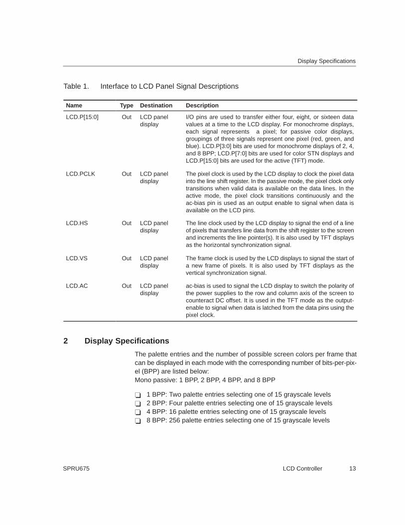
Table 1 shows details relating to the LCD controller signals.
Display Specifications
13LCD ControllerSPRU675
Table 1. Interface to LCD Panel Signal Descriptions
Name Type Destination Description
LCD.P[15:0] Out LCD panel display
I/O pins are used to transfer either four, eight, or sixteen datavalues at a time to the LCD display. For monochrome displays,each signal represents a pixel; for passive color displays,groupings of three signals represent one pixel (red, green, andblue). LCD.P[3:0] bits are used for monochrome displays of 2, 4,and 8 BPP; LCD.P[7:0] bits are used for color STN displays andLCD.P[15:0] bits are used for the active (TFT) mode.
LCD.PCLK Out LCD panel display
The pixel clock is used by the LCD display to clock the pixel datainto the line shift register. In the passive mode, the pixel clock onlytransitions when valid data is available on the data lines. In theactive mode, the pixel clock transitions continuously and theac-bias pin is used as an output enable to signal when data isavailable on the LCD pins.
LCD.HS Out LCD panel display
The line clock used by the LCD display to signal the end of a lineof pixels that transfers line data from the shift register to the screenand increments the line pointer(s). It is also used by TFT displaysas the horizontal synchronization signal.
LCD.VS Out LCD panel display
The frame clock is used by the LCD displays to signal the start ofa new frame of pixels. It is also used by TFT displays as thevertical synchronization signal.
LCD.AC Out LCD panel display
ac-bias is used to signal the LCD display to switch the polarity ofthe power supplies to the row and column axis of the screen tocounteract DC offset. It is used in the TFT mode as the output-enable to signal when data is latched from the data pins using thepixel clock.
2 Display Specifications
The palette entries and the number of possible screen colors per frame thatcan be displayed in each mode with the corresponding number of bits-per-pix-el (BPP) are listed below:Mono passive: 1 BPP, 2 BPP, 4 BPP, and 8 BPP
� 1 BPP: Two palette entries selecting one of 15 grayscale levels� 2 BPP: Four palette entries selecting one of 15 grayscale levels� 4 BPP: 16 palette entries selecting one of 15 grayscale levels� 8 BPP: 256 palette entries selecting one of 15 grayscale levels

Display Specifications
LCD Controller14 SPRU675
Color passive: 2 BPP, 4 BPP, 8 BPP, 12, and 16 BPP
� 2 BPP: Four palette entries selecting from 3375 possible colors� 4 BPP: 16 palette entries selecting from 3375 possible colors� 8 BPP: 256 palette entries selecting from 3375 possible colors� 12 BPP: 3375 possible on-screen colors� 16 BPP: 3375 possible on-screen colors
Active: 2 BPP, 4BPP, 8BPP, 12 BPP, and 16BPP
� 2 BPP: Four palette entries selecting from 4096 colors� 4 BPP: 16 palette entries selecting from 4096 colors� 8 BPP: 256 palette entries selecting from 4096 colors� 12 BPP: Maximum 64K colors� 16 BPP: Maximum 64K colors, depending on the LCD panel
Palette entries are 16 bits wide (2 bytes) and therefore 2 and 4 BPP require32 bytes of storage. 8 BPP modes require 512 bytes. 12 or 16 BPP modes donot use palette data but need the bits-per-pixel information to be loaded.These modes use 32 bytes similar to the 2 and 4 BPP modes.
The mono passive mode supports two different interfaces: 4-bit panel and 8-bitpanel. All modes (color/mono, 2, 4, 8, 12, or 16 bits-per-pixel) operateindependently of each other.
The vertical synchronization signal (VSYNC) width must be programmed to beas small as possible on passive screen modes, but long enough to load thepalette without stealing all the memory bandwidth from the MPU. To satisfy thesystem requirement, the following equation must be met:
�256 � (15 * FDD)� � ��HBP � HFP �(PPL � 1)
d� HSW � 3� * VSW * PCD�
d Display
1 TFT
2 2/3 STN color
4 Mono 4 bits
Note: If the condition is not true, the LCD controller displays a black screen every other frame.
Pixels-per-line (PPL) must be in multiples of 16. Most LCD panels ignore dataat the right hand side of the screen at the end of the line that is not needed .
LCD Controller Operation
15LCD ControllerSPRU675
3 LCD Controller Operation
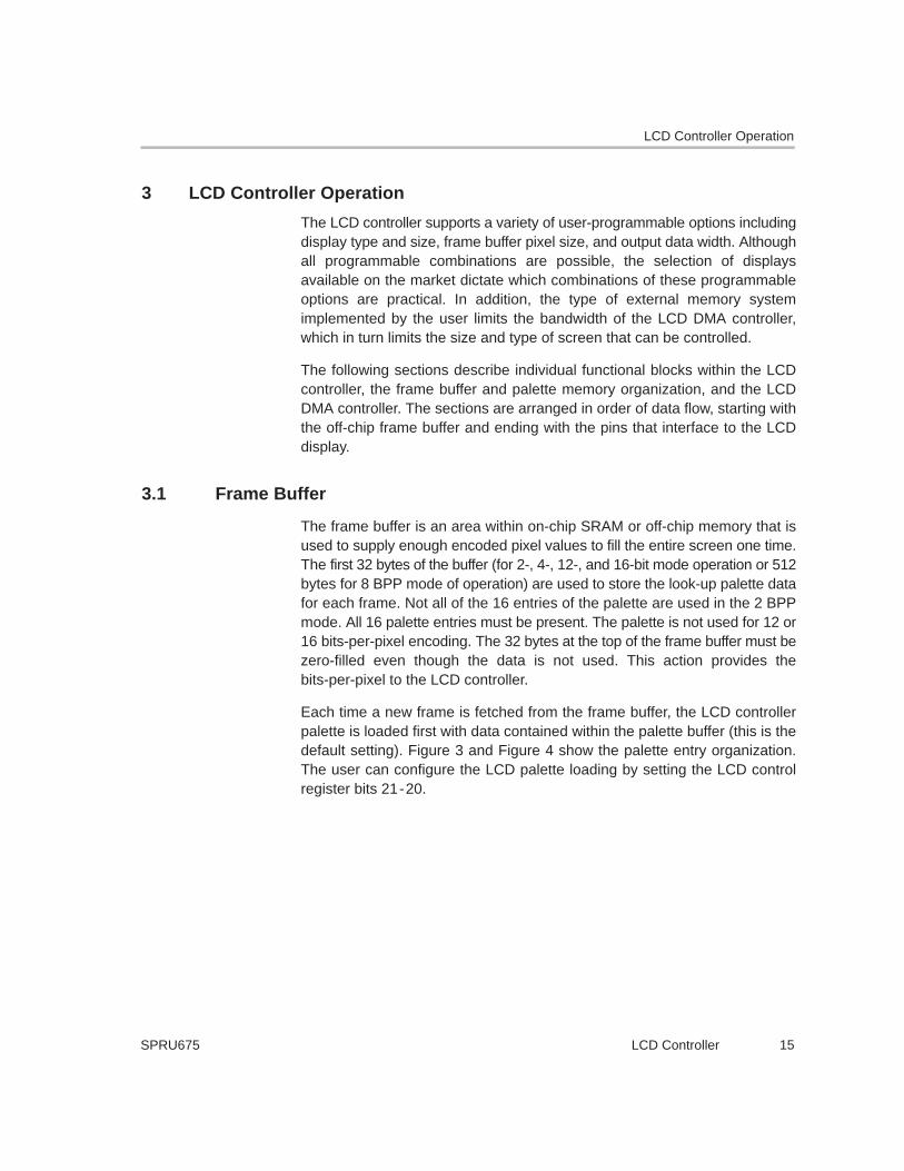
The LCD controller supports a variety of user-programmable options includingdisplay type and size, frame buffer pixel size, and output data width. Althoughall programmable combinations are possible, the selection of displaysavailable on the market dictate which combinations of these programmableoptions are practical. In addition, the type of external memory systemimplemented by the user limits the bandwidth of the LCD DMA controller,which in turn limits the size and type of screen that can be controlled.
The following sections describe individual functional blocks within the LCDcontroller, the frame buffer and palette memory organization, and the LCDDMA controller. The sections are arranged in order of data flow, starting withthe off-chip frame buffer and ending with the pins that interface to the LCDdisplay.
3.1 Frame Buffer
The frame buffer is an area within on-chip SRAM or off-chip memory that isused to supply enough encoded pixel values to fill the entire screen one time.The first 32 bytes of the buffer (for 2-, 4-, 12-, and 16-bit mode operation or 512bytes for 8 BPP mode of operation) are used to store the look-up palette datafor each frame. Not all of the 16 entries of the palette are used in the 2 BPPmode. All 16 palette entries must be present. The palette is not used for 12 or16 bits-per-pixel encoding. The 32 bytes at the top of the frame buffer must bezero-filled even though the data is not used. This action provides thebits-per-pixel to the LCD controller.
Each time a new frame is fetched from the frame buffer, the LCD controllerpalette is loaded first with data contained within the palette buffer (this is thedefault setting). Figure 3 and Figure 4 show the palette entry organization.The user can configure the LCD palette loading by setting the LCD controlregister bits 21-20.

LCD Controller Operation
LCD Controller16 SPRU675
Figure 3. 256 Palette Entry/Buffer Format (8 BPP)
Individual Palette Entry
Bit 15 14 13 12 11 10 9 8 7 6 5 4 3 2 1 0
Color n/u BPP† Red (R) Green (G) Blue (B)
Bit 15 14 13 12 11 10 9 8 7 6 5 4 3 2 1 0
Mono n/u BPP† Unused Mono (M)
† Bits-per-pixel (BPP) is only contained within the first palette entry (palette entry0).
256 Entry Palette Buffer
Bit 15 0
Base + 0x0 Palette entry 0
Base + 0x2 Palette entry 1
Base + 0x1FC Palette entry 254
Base + 0x1FE Palette entry 255
Base + 0x200 Start of pixel data
Figure 4. 16 Palette Entry/Buffer Format (1, 2, 4, 12, 16 BPP)
16 Entry Palette Buffer
Bit 15 0
Base + 0x0 Palette entry 0
Base + 0x2 Palette entry 1
Base + 0x1C Palette entry 14
Base + 0x1E Palette entry 15
Base + 0x20 Start of pixel data
LCD Controller Operation
17LCD ControllerSPRU675
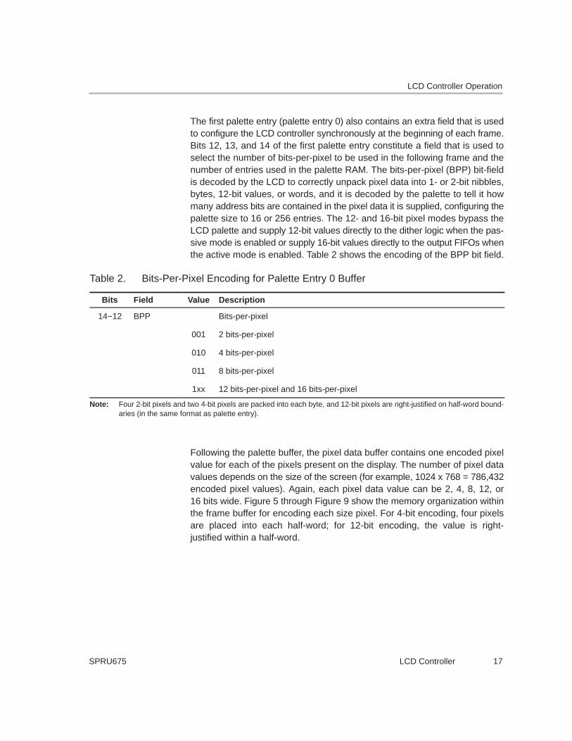
The first palette entry (palette entry 0) also contains an extra field that is usedto configure the LCD controller synchronously at the beginning of each frame.Bits 12, 13, and 14 of the first palette entry constitute a field that is used toselect the number of bits-per-pixel to be used in the following frame and thenumber of entries used in the palette RAM. The bits-per-pixel (BPP) bit-fieldis decoded by the LCD to correctly unpack pixel data into 1- or 2-bit nibbles,bytes, 12-bit values, or words, and it is decoded by the palette to tell it howmany address bits are contained in the pixel data it is supplied, configuring thepalette size to 16 or 256 entries. The 12- and 16-bit pixel modes bypass theLCD palette and supply 12-bit values directly to the dither logic when the pas-sive mode is enabled or supply 16-bit values directly to the output FIFOs whenthe active mode is enabled. Table 2 shows the encoding of the BPP bit field.
Table 2. Bits-Per-Pixel Encoding for Palette Entry 0 Buffer
Bits Field Value Description
14−12 BPP Bits-per-pixel
001 2 bits-per-pixel
010 4 bits-per-pixel
011 8 bits-per-pixel
1xx 12 bits-per-pixel and 16 bits-per-pixel
Note: Four 2-bit pixels and two 4-bit pixels are packed into each byte, and 12-bit pixels are right-justified on half-word bound-aries (in the same format as palette entry).
Following the palette buffer, the pixel data buffer contains one encoded pixelvalue for each of the pixels present on the display. The number of pixel datavalues depends on the size of the screen (for example, 1024 x 768 = 786,432encoded pixel values). Again, each pixel data value can be 2, 4, 8, 12, or16 bits wide. Figure 5 through Figure 9 show the memory organization withinthe frame buffer for encoding each size pixel. For 4-bit encoding, four pixelsare placed into each half-word; for 12-bit encoding, the value is right-justified within a half-word.

LCD Controller Operation
LCD Controller18 SPRU675
Figure 5. 2 BPP Frame Buffer Memory Organization
Frame Buffer Byte Address 7 0
Base P0 P1 P2 P3
Base + 1 P4 P5 P6 P7
Base + 2 P8 P9 P10 P11
Base + 3 P12 P13 P14 P15
www
•••
•••
•••
Figure 6. 4 BPP Frame Buffer Memory Organization
Frame Buffer Byte Address 7 0
Base P0 P1
Base + 1 P2 P3
Base + 2 P4 P5
Base + 3 P6 P7
www
•••
Figure 7. 8 BPP Frame Buffer Memory Organization
Frame Buffer Byte Address 7 0
Base P0
Base + 1 P1
Base + 2 P2
Base + 3 P3
www

LCD Controller Operation
19LCD ControllerSPRU675
Figure 8. 12 BPP Frame Buffer Memory Organization
Frame Buffer Byte Address 7 0
Base P0[7:0]
Base + 1 Unused P0[11:8]
Base + 2 P1[7:0]
Base + 3 Unused P1[11:8]
•••
•••
Figure 9. 16 BPP Frame Buffer Memory Organization
Frame Buffer Byte Address 7 0
Base P0[7:0]
Base + 1 P0[15:8]
Base + 2 P1[7:0]
Base + 3 P1[15:8]
•••
The OMAP5910 MPU operates in little-endian mode and the number and posi-tion of pixels in an access depend on access type (byte, half-word, or word).For example, if the LCD controller is in the 2 BPP mode and the MPU performsa read at the beginning of the frame buffer, the result of the read is:
Byte access (8-bit read):
P0 P1 P2 P3
Half-word access (16-bit read):
P4 P5 P6 P7 P0 P1 P2 P3
Word access (32-bit read):
P12 P13 P14 P15 P8 P9 P10 P11 P4 P5 P6 P7 P0 P1 P2 P3

Lookup Palette
LCD Controller20 SPRU675
The pixel data is stored in the frame buffer the same way in all three cases (asshown in Figure 5); only the little-endian accesses of the MPU result in the dif-ferent pixel positions of each access.
The top and bottom addresses of the frame buffer (palette entries plus pixeldata) are programmed in the DMA controller. A synchronization interruptoccurs if the LCD display information settings such as pixels-per-line, lines-per-frame, color/monochrome mode, or bits-per-pixel that are programmed bythe user are not in accordance with the size of the frame buffer as programmedin the DMA.
The following equations are used to calculate the total frame buffer size (inbytes) to be programmed in the system DMA based on varying pixel sizeencoding and screen sizes.
For 2 bits�pixel : FrameBufferSize � 32 �(Lines * Columns)
4
For 4 bits�pixel : FrameBufferSize � 32 �(Lines * Columns)
2
For 8 bits�pixel : FrameBufferSize � 512 � (Lines * Columns)
For 12�16 bits�pixel : FrameBufferSize � 32 � 2(Lines * Columns)
4 Lookup Palette
The encoded pixel data from the input FIFO is used as an address to index andselect individual palette locations: 2-bit pixels address four locations, 4-bitpixels address sixteen locations, and 8-bit pixels select any of the 256 paletteentries.
When a palette entry is selected by the encoded pixel value, the contents ofthe entry are sent to the color/grayscale space/time base dither circuit. In colormode, the value within the palette is made up of three, 4-bit fields, one for eachcolor component: red, green, and blue. In the monochrome mode, only one4-bit value is present. For both modes, the 4-bit values represent 1 of 15 inten-sity levels. For color operation, an individual frame is limited to a selection of256 colors (the number of palette entries). The LCD controller, however, cangenerate a total of 3375 colors (15 levels per color x 3 colors). When a 12 or16 bit-per-pixel mode is enabled, the palette is bypassed. For passivedisplays, 12-bit pixels and 16-bit pixels are sent directly to the dither logic.

Color/Grayscale Dithering
21LCD ControllerSPRU675
5 Color/Grayscale Dithering
Entries selected from the lookup palette are sent to the color/grayscale space/timebase dither generator. Each 4-bit value is used to select one of 15 intensitylevels. Two of the 16 dither values are identical (most intense). The gray/colorintensity is controlled by turning individual pixels on and off at varying periodicrates. More intense grays/colors are produced by making the average timethat the pixel is off longer than the average time that it is on. The dither genera-tor also uses the intensity of adjacent pixels in its calculations to give thescreen image a smooth appearance. The proprietary dither algorithm is opti-mized to provide a range of intensity values that match the visual perceptionof color/gray gradations. In color mode, three separate dither blocks are usedto process the three color components: red, green, and blue.
The duty cycle and resultant intensity level for all 15 color/grayscale levels issummarized in Table 3.
Table 3. Color/Grayscale Intensities and Modulation Rates
Dither Value(4-Bit Value From Palette)
Intensity(0% is White)
Modulation Rate(Ratio of ON to ON+OFF Pixels)
0000 0.0% 0
0001 11.1% 1/9
0010 20.0% 1/5
0011 26.7% 4/15
0100 33.3% 3/9
0101 40.0% 2/5
0110 44.4% 4/9
0111 50.0% 1/2
1000 55.6% 5/9
1001 60.0% 3/5
1010 66.6% 6/9
1011 73.3% 11/15
1100 80.0% 4/5
1101 88.9% 8/9
1110 100.0% 1
1111 100.0% 1
Output FIFO
LCD Controller22 SPRU675
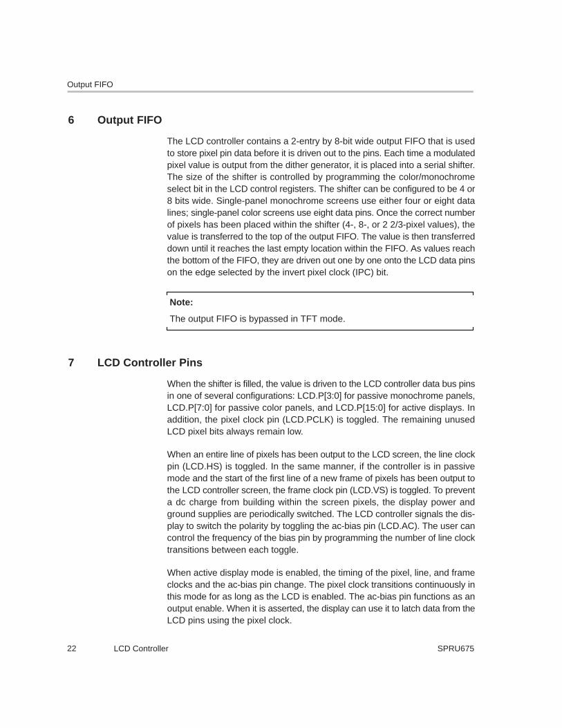
6 Output FIFO
The LCD controller contains a 2-entry by 8-bit wide output FIFO that is usedto store pixel pin data before it is driven out to the pins. Each time a modulatedpixel value is output from the dither generator, it is placed into a serial shifter.The size of the shifter is controlled by programming the color/monochromeselect bit in the LCD control registers. The shifter can be configured to be 4 or8 bits wide. Single-panel monochrome screens use either four or eight datalines; single-panel color screens use eight data pins. Once the correct numberof pixels has been placed within the shifter (4-, 8-, or 2 2/3-pixel values), thevalue is transferred to the top of the output FIFO. The value is then transferreddown until it reaches the last empty location within the FIFO. As values reachthe bottom of the FIFO, they are driven out one by one onto the LCD data pinson the edge selected by the invert pixel clock (IPC) bit.
Note:
The output FIFO is bypassed in TFT mode.
7 LCD Controller Pins
When the shifter is filled, the value is driven to the LCD controller data bus pinsin one of several configurations: LCD.P[3:0] for passive monochrome panels,LCD.P[7:0] for passive color panels, and LCD.P[15:0] for active displays. Inaddition, the pixel clock pin (LCD.PCLK) is toggled. The remaining unusedLCD pixel bits always remain low.
When an entire line of pixels has been output to the LCD screen, the line clockpin (LCD.HS) is toggled. In the same manner, if the controller is in passivemode and the start of the first line of a new frame of pixels has been output tothe LCD controller screen, the frame clock pin (LCD.VS) is toggled. To preventa dc charge from building within the screen pixels, the display power andground supplies are periodically switched. The LCD controller signals the dis-play to switch the polarity by toggling the ac-bias pin (LCD.AC). The user cancontrol the frequency of the bias pin by programming the number of line clocktransitions between each toggle.
When active display mode is enabled, the timing of the pixel, line, and frameclocks and the ac-bias pin change. The pixel clock transitions continuously inthis mode for as long as the LCD is enabled. The ac-bias pin functions as anoutput enable. When it is asserted, the display can use it to latch data from theLCD pins using the pixel clock.

LCD Controller Pins
23LCD ControllerSPRU675
The timing of the line and frame clock pins is programmable to support bothpassive and active mode. Programming options include:
� Delay insertion both at the beginning and end of each line and frame (frontand back porch)
� Pixel clock, line clock, frame clock, and ac-bias signal polarity� Line and frame clock pulse width
If the LCD is disabled, the signals LCD.P[15:0] are set to 0 and LCD.PCLK,LCD.VS, LCD.HS, and LCD.AC are set to their inactive state. This can be 0or 1 depending on the inversions programmed in the timing 2 register. SeeTable 24.
The OMAP5910 LCD controller provides outputs compatible with passivemonochrome, passive color (STN), and active color (TFT) displays. Recom-mended connections to each type of display are outlined in the sections below.
7.1 Passive Monochrome Panels
Passive monochrome displays can be supported for graphics depths of 8 BPP(256 entry palette), 4 BPP, 2 BPP, or 1 BPP. For passive monochrome displays,four signals are supplied. Each signal represents one pixel that is dithered oversuccessive frames to achieve a maximum of 15 gray levels (see Table 4).
Table 4. Passive Monochrome Panel Inputs
OMAP5910 LCD Controller OutputPassive Monochrome
Panel Input
LCD.P[0] (leftmost pixel) D[3]
LCD.P[1] D[2]
LCD.P[2] D[1]
LCD.P[3] (rightmost pixel) D[0]
LCD Controller Pins
LCD Controller24 SPRU675
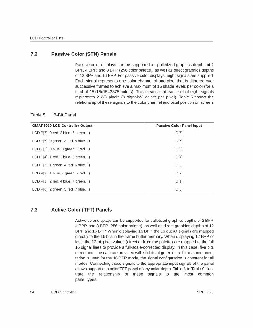
7.2 Passive Color (STN) Panels
Passive color displays can be supported for palletized graphics depths of 2BPP, 4 BPP, and 8 BPP (256 color palette), as well as direct graphics depthsof 12 BPP and 16 BPP. For passive color displays, eight signals are supplied.Each signal represents one color channel of one pixel that is dithered oversuccessive frames to achieve a maximum of 15 shade levels per color (for atotal of 15x15x15=3375 colors). This means that each set of eight signalsrepresents 2 2/3 pixels (8 signals/3 colors per pixel). Table 5 shows therelationship of these signals to the color channel and pixel position on screen.
Table 5. 8-Bit Panel
OMAP5910 LCD Controller Output Passive Color Panel Input
LCD.P[7] (0 red, 2 blue, 5 green…) D[7]
LCD.P[6] (0 green, 3 red, 5 blue…) D[6]
LCD.P[5] (0 blue, 3 green, 6 red…) D[5]
LCD.P[4] (1 red, 3 blue, 6 green…) D[4]
LCD.P[3] (1 green, 4 red, 6 blue…) D[3]
LCD.P[2] (1 blue, 4 green, 7 red…) D[2]
LCD.P[1] (2 red, 4 blue, 7 green…) D[1]
LCD.P[0] (2 green, 5 red, 7 blue…) D[0]
7.3 Active Color (TFT) Panels
Active color displays can be supported for palletized graphics depths of 2 BPP,4 BPP, and 8 BPP (256 color palette), as well as direct graphics depths of 12BPP and 16 BPP. When displaying 16 BPP, the 16 output signals are mappeddirectly to the 16 bits in the frame buffer memory. When displaying 12 BPP orless, the 12-bit pixel values (direct or from the palette) are mapped to the full16 signal lines to provide a full-scale-corrected display. In this case, five bitsof red and blue data are provided with six bits of green data. If this same orien-tation is used for the 16 BPP mode, the signal configuration is constant for allmodes. Connecting these signals to the appropriate input signals of the panelallows support of a color TFT panel of any color depth. Table 6 to Table 9 illus-trate the relationship of these signals to the most commonpanel types.

LCD Controller Pins
25LCD ControllerSPRU675
Note:
The actual number of colors displayed is limited to the smaller of 2output depth
and 2panel input pins.
Connecting a 12-bit panel for 16 BPP operation involves truncating the 16 bitsof data to the 12 bits required by the panel (see Table 6).
Table 6. 16-Bits-Per-Pixel and 12-Bit Panel
OMAP5910 LCD Controller Output 12-Bit TFT Panel Input
LCD.P[15] (red[4]) red[3]
LCD.P[14] (red[3]) red[2]
LCD.P[13] (red[2]) red[1]
LCD.P[12] (red[1]) red[0]
LCD.P[11] (red[0]) n/c
LCD.P[10] (green[5]) green[3]
LCD.P[9] (green[4]) green[2]
LCD.P[8] (green[3]) green[1]
LCD.P[7] (green[2]) green[0]
LCD.P[6] (green[1]) n/c
LCD.P[5] (green[0]) n/c
LCD.P[4] (blue[4]) blue[3]
LCD.P[3] (blue[3]) blue[2]
LCD.P[2] (blue[2]) blue[1]
LCD.P[1] (blue[1]) blue[0]
LCD.P[0] (blue[0]) n/c

LCD Controller Pins
LCD Controller26 SPRU675
Connecting a 15-bit panel for 16 BPP operation involves truncating the 16 bitsof data to the 15 bits required by the panel (see Table 7).
Table 7. 16-Bits-Per-Pixel and 15-Bit Panel
OMAP5910 LCD Controller Output 12-Bit TFT Panel Input
LCD.P[15] (red[4]) red[4]
LCD.P[14] (red[3]) red[3]
LCD.P[13] (red[2]) red[2]
LCD.P[12] (red[1]) red[1]
LCD.P[11] (red[0]) red[0]
LCD.P[10] (green[5]) green[4]
LCD.P[9] (green[4]) green[3]
LCD.P[8] (green[3]) green[2]
LCD.P[7] (green[2]) green[1]
LCD.P[6] (green[1]) green[0]
LCD.P[5] (green[0]) n/c
LCD.P[4] (blue[4]) blue[4]
LCD.P[3] (blue[3]) blue[3]
LCD.P[2] (blue[2]) blue[2]
LCD.P[1] (blue[1]) blue[1]
LCD.P[0] (blue[0]) blue[0]
Connecting an 18-bit panel for 16 BPP operation involves replicating (note *’sbelow) the 16 bits of data to fill in the entire 18 bits required by the panel. Thisis preferable to hardwiring the extra bits to a constant value, which reduces thedynamic range of the display and causes a color error (see Table 8).
Table 8. 16-Bits-Per-Pixel and 18-Bit Panel
OMAP5910 LCD Controller Output 18-Bit TFT Panel Input
LCD.P[15] (red[4]) red[5]
LCD.P[14] (red[3]) red[4]
LCD.P[13] (red[2]) red[3]
LCD.P[12] (red[1]) red[2]
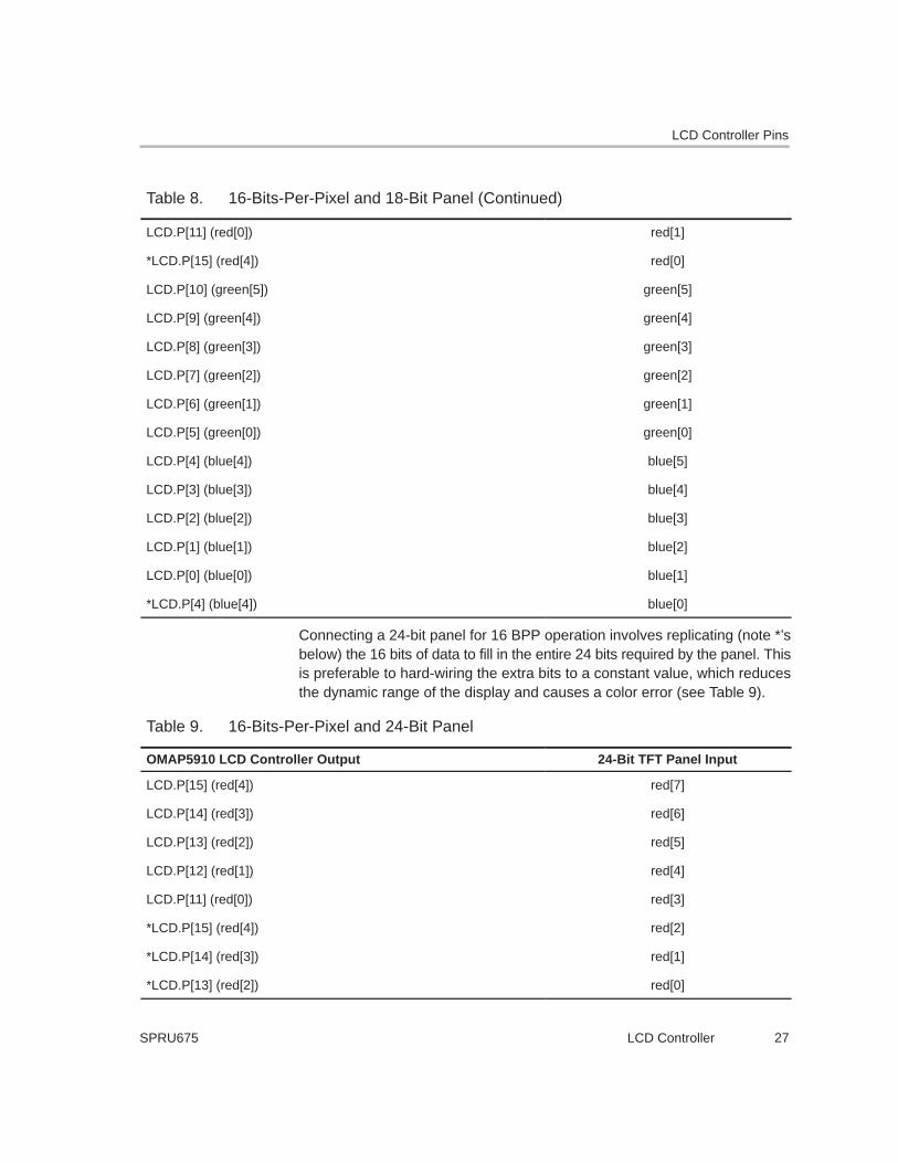
LCD Controller Pins
27LCD ControllerSPRU675
Table 8. 16-Bits-Per-Pixel and 18-Bit Panel (Continued)
LCD.P[11] (red[0]) red[1]
*LCD.P[15] (red[4]) red[0]
LCD.P[10] (green[5]) green[5]
LCD.P[9] (green[4]) green[4]
LCD.P[8] (green[3]) green[3]
LCD.P[7] (green[2]) green[2]
LCD.P[6] (green[1]) green[1]
LCD.P[5] (green[0]) green[0]
LCD.P[4] (blue[4]) blue[5]
LCD.P[3] (blue[3]) blue[4]
LCD.P[2] (blue[2]) blue[3]
LCD.P[1] (blue[1]) blue[2]
LCD.P[0] (blue[0]) blue[1]
*LCD.P[4] (blue[4]) blue[0]
Connecting a 24-bit panel for 16 BPP operation involves replicating (note *’sbelow) the 16 bits of data to fill in the entire 24 bits required by the panel. Thisis preferable to hard-wiring the extra bits to a constant value, which reducesthe dynamic range of the display and causes a color error (see Table 9).
Table 9. 16-Bits-Per-Pixel and 24-Bit Panel
OMAP5910 LCD Controller Output 24-Bit TFT Panel Input
LCD.P[15] (red[4]) red[7]
LCD.P[14] (red[3]) red[6]
LCD.P[13] (red[2]) red[5]
LCD.P[12] (red[1]) red[4]
LCD.P[11] (red[0]) red[3]
*LCD.P[15] (red[4]) red[2]
*LCD.P[14] (red[3]) red[1]
*LCD.P[13] (red[2]) red[0]

LCD Controller Registers
LCD Controller28 SPRU675
Table 9. 16-Bits-Per-Pixel and 24-Bit Panel (Continued)
OMAP5910 LCD Controller Output 24-Bit TFT Panel Input
LCD.P[10] (green[5]) green[7]
LCD.P[9] (green[4]) green[6]
LCD.P[8] (green[3]) green[5]
LCD.P[7] (green[2]) green[4]
LCD.P[6] (green[1]) green[3]
LCD.P[5] (green[0]) green[2]
*LCD.P[10] (green[5]) green[1]
*LCD.P[9] (green[4]) green[0]
LCD.P[4] (blue[4]) blue[7]
LCD.P[3] (blue[3]) blue[6]
LCD.P[2] (blue[2]) blue[5]
LCD.P[1] (blue[1]) blue[4]
LCD.P[0] (blue[0]) blue[3]
*LCD.P[4] (blue[4]) blue[2]
*LCD.P[3] (blue[3]) blue[1]
*LCD.P[2] (blue[2]) blue[0]
8 LCD Controller Registers
The LCD controller contains four control registers and one status register.
The control registers contain bit fields to enable and disable the LCD controllerto define:
� The height and width of the screen being controlled� Color or monochrome mode� Passive or active display� Polarity of the control lines� Pulse width of the line and frame clocks� The pixel clock and ac-bias frequency� The number of delays to insert before/after each line and after each frame

LCD Controller Registers
29LCD ControllerSPRU675
An additional control field exists to tune the DMA performance based on thetype of memory system in which the LCD controller is used. This field controlsthe placement of a minimum delay between each LCD palette request toensure enough bus bandwidth is given to other systems access. This field isonly used for palette loading.
The status register contains bits that signal:
� FIFO underrun error
� Frame synchronization error
� When the last active frame has completed after the LCD is disabled(maskable)
� ac counter, if programmed
Each of these hardware-detected events signals an interrupt request to theinterrupt controller.
Table 10 lists the LCD controller registers. Table 11 through Table 23 describethe register bits.
Table 10. LCD Controller Registers
Register Description R/W Size Address
LcdControl LCD control R/W 32 bits FFFE:C000
LcdTiming0 LCD timing 0 R/W 32 bits FFFE:C004
LcdTiming1 LCD timing 1 R/W 32 bits FFFE:C008
LcdTiming2 LCD timing 2 R/W 32 bits FFFE:C00C
LcdStatus LCD status R/W 32 bits FFFE:C010
LcdSubpanel LCD subpanel display R/W 32 bits FFFE:C014
8.1 LCD Control Register 1 (LCDControl)
Table 11. LCD Control Register (LCDControl)
Bits Field Value DescriptionResetValue
31−25 − Reserved 0
24 5-6-5 STN 12 BPP (5-6-5) mode 0
0 On

LCD Controller Registers
LCD Controller30 SPRU675
Table 11. LCD Control Register (LCDControl) (Continued)
BitsResetValueDescriptionValueField
1 Off
16 bits of data are in the frame buffer, but only 12 bits are ditheredand sent out.
23 TFT Map TFT alternate signal mapping: 0
0 Output pixel data for 1, 2, 4, and 8 BPP modes are right aligned onLCD pins (11:0)
1 Output pixel data for 1, 2, 4, and 8 BPP are converted to 5-6-5format using pins (15:0)R3 R2 R1 R0 R3 G3 G2 G1 G0 G3 G2 B3 B2 B1 B0 B3
22 LCDCB1 LCD control bit 1
See Table 16 for proper settings for this field.
0
21−20 PLM Palette loading mode. Must precede data-loading-only mode. 0
00 Palette and data loading, reset value
01 Palette loading
10 Data loading
19−12 FDD FIFO DMA request delay
Encoded value (0–255) used to specify the number of memorycontroller clocks. The input FIFO DMA request must be disabled.The clock count starts after 16 words read in the input FIFO.Programming FDD = 00h disables this function.
0
11−10 − Reserved 0
9 M8B Mono 8-bit mode. Selects 4 or 8 data lines to output pixel data to thescreen.
0
0 LCD_PIXEL[3:0] is used to output four pixel values to the paneleach pixel clock transition.
1 LCD_PIXEL[7:0] is used to output eight pixel values to the paneleach pixel clock transition.
This bit is ignored in all other modes.
8 LCDCB0 LCD control bit 0. Used with LCD control bit 1 to control mappingof pixel data from the frame buffer to the output bus LCD.P[16:0].
See Table 16 for proper settings for this field.
0

LCD Controller Registers
31LCD ControllerSPRU675
Table 11. LCD Control Register (LCDControl) (Continued)
BitsResetValueDescriptionValueField
7 LCDTFT LCD TFT 0
0 Passive or STN display operation enabled, dither logic is enabled
1 Active or TFT display operation enabled, external palette and DACrequired, dither logic bypassed, pin timing changes to supportcontinuous pixel clock, output enable, VSYNC, HSYNC signals
5−6 − Reserved 0
4 LoadMask Load mask 0
0 Mask out the loaded palette interrupt
1 Mask not active
3 DoneMask Done mask 0
0 Mask out the frame done (done) interrupt
1 Mask not active
2 - Reserved 0
1 LCDBW LCD Monochrome 0
0 Color operation enable
1 Monochrome operation enabled
0 LCDEN LCD controller enable 0
0 LCD controller disabled
1 LCD controller enabled
Table 12 lists suggested LCD register settings for various operating modes.
Table 12. LCD Control Register Settings
Panel Type Graphics Mode Register SettingFirst Palette
Entry
Monochrome 2 BPP 0x00400002 0x1XXX
Monochrome 4 BPP 0x00400002 0x2XXX
Monochrome 8 BPP 0x00010002 0x3XXX
Passive color 2 BPP 0x00400000 0x1XXX
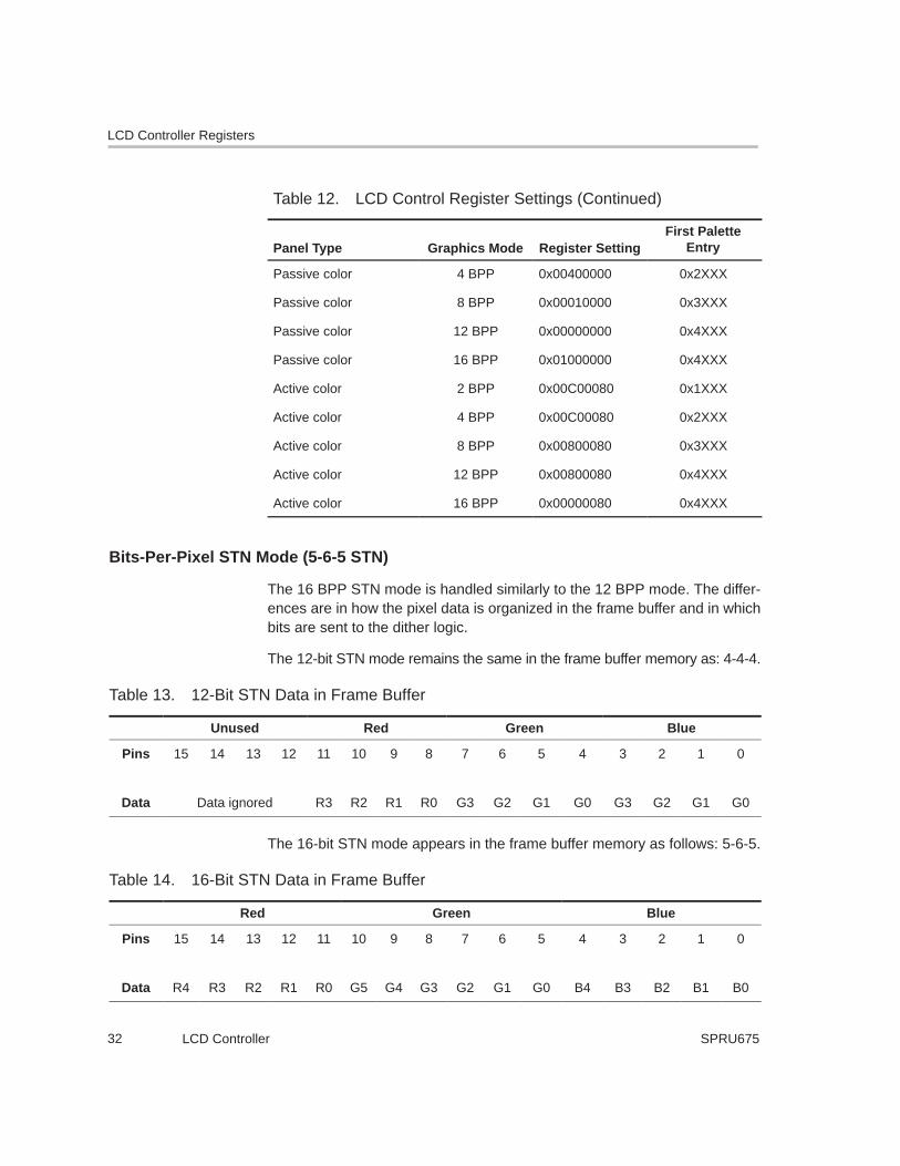
LCD Controller Registers
LCD Controller32 SPRU675
Table 12. LCD Control Register Settings (Continued)
Panel TypeFirst Palette
EntryRegister SettingGraphics Mode
Passive color 4 BPP 0x00400000 0x2XXX
Passive color 8 BPP 0x00010000 0x3XXX
Passive color 12 BPP 0x00000000 0x4XXX
Passive color 16 BPP 0x01000000 0x4XXX
Active color 2 BPP 0x00C00080 0x1XXX
Active color 4 BPP 0x00C00080 0x2XXX
Active color 8 BPP 0x00800080 0x3XXX
Active color 12 BPP 0x00800080 0x4XXX
Active color 16 BPP 0x00000080 0x4XXX
Bits-Per-Pixel STN Mode (5-6-5 STN)
The 16 BPP STN mode is handled similarly to the 12 BPP mode. The differ-ences are in how the pixel data is organized in the frame buffer and in whichbits are sent to the dither logic.
The 12-bit STN mode remains the same in the frame buffer memory as: 4-4-4.
Table 13. 12-Bit STN Data in Frame Buffer
Unused Red Green Blue
Pins 15 14 13 12 11 10 9 8 7 6 5 4 3 2 1 0
Data Data ignored R3 R2 R1 R0 G3 G2 G1 G0 G3 G2 G1 G0
The 16-bit STN mode appears in the frame buffer memory as follows: 5-6-5.
Table 14. 16-Bit STN Data in Frame Buffer
Red Green Blue
Pins 15 14 13 12 11 10 9 8 7 6 5 4 3 2 1 0
Data R4 R3 R2 R1 R0 G5 G4 G3 G2 G1 G0 B4 B3 B2 B1 B0
LCD Controller Registers
33LCD ControllerSPRU675
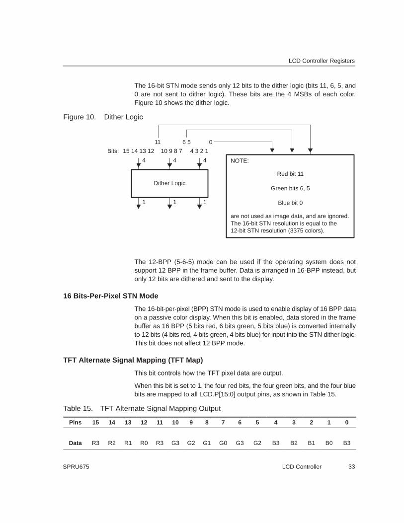
The 16-bit STN mode sends only 12 bits to the dither logic (bits 11, 6, 5, and0 are not sent to dither logic). These bits are the 4 MSBs of each color.Figure 10 shows the dither logic.
Figure 10. Dither Logic
4
are not used as image data, and are ignored.The 16-bit STN resolution is equal to the12-bit STN resolution (3375 colors).
NOTE:
Red bit 11
Green bits 6, 5
Blue bit 0
Dither Logic
Bits: 15 14 13 12 10 9 8 7 4 3 2 1
11 06 5
1
4
1
4
1
The 12-BPP (5-6-5) mode can be used if the operating system does notsupport 12 BPP in the frame buffer. Data is arranged in 16-BPP instead, butonly 12 bits are dithered and sent to the display.
16 Bits-Per-Pixel STN Mode
The 16-bit-per-pixel (BPP) STN mode is used to enable display of 16 BPP dataon a passive color display. When this bit is enabled, data stored in the framebuffer as 16 BPP (5 bits red, 6 bits green, 5 bits blue) is converted internallyto 12 bits (4 bits red, 4 bits green, 4 bits blue) for input into the STN dither logic.This bit does not affect 12 BPP mode.
TFT Alternate Signal Mapping (TFT Map)
This bit controls how the TFT pixel data are output.
When this bit is set to 1, the four red bits, the four green bits, and the four bluebits are mapped to all LCD.P[15:0] output pins, as shown in Table 15.
Table 15. TFT Alternate Signal Mapping Output
Pins 15 14 13 12 11 10 9 8 7 6 5 4 3 2 1 0
Data R3 R2 R1 R0 R3 G3 G2 G1 G0 G3 G2 B3 B2 B1 B0 B3

LCD Controller Registers
LCD Controller34 SPRU675
When this bit is set to 0 (default), the four red bits, the four green bits, and thefour blue bits are right aligned on LCD.P[11:0] pins. The upper LCD.P[15:12]are set to 0.
LCD Control Bit 1
The LCD control bit 1 is used along with LCD control bit 0 to control themapping of pixel data from the frame buffer to the output bus LCD.P[15:0].Table 16 shows the appropriate settings for this bit.
Table 16. Control Bit 0 And Control Bit 1 Mapping by Display Types
Display Type Mode Control Bit 0 Control Bit 1
Passive monochrome 2 BPP 0 1
4 BPP 0 1
8 BPP 0 0
Passive color 8 BPP 0 0
12 BPP 0 0
TFT 16 BPP 0 0
LCD TFT (LCDTFT)
The LCD TFT (LCDTFT) bit selects whether the LCD controller operates inpassive (STN) or active (TFT) display control mode. When LCDTFT = 0:passive or STN mode is selected; all LCD data flow operates normally(including the use of the LCD dither logic); and all LCD controller pin timingoperates as described in Section 7, LCD Controller Pins. When LCDTFT = 1,active or TFT mode is selected. Frame data is transferred via the DMA fromoff-chip memory to the input FIFO, is unpacked, and is used to select an entryfrom the palette (for 1, 2, 4, and 8 bits-per-pixel modes), just as for passivemode (see Figure 11).

LCD Controller Registers
35LCD ControllerSPRU675
Figure 11. Passive Mode Pixel Clock and Data Pin Timing
Data PinsChange
LCD.PCLK
LCD.P [3:0]
LCD.HS
LCD.VS
Pixel 0through 3
Pixel 4through 7
Pixel 8through 11
Pixel 12through 15
Data Pins Samplesby the Display
LCDTFT=0M8B=0IPC=0
The value read from the palette bypasses the LCD dither logic and is sent di-rectly to the output FIFO to be output on the LCD data pins. In the TFT mode,the pixel size within the frame buffer is increased to 16 bits when 12- or 16-bitpixel encoding mode is enabled (BPP = 1XX). Thus, two 16-bit values arepacked into each word in the frame buffer. See Figure 12.

LCD Controller Registers
LCD Controller36 SPRU675
Figure 12. Active Mode Pixel Clock and Data Pin Timing
Data PinsChange
LCD.PCLK
LCD.P [3:0]
LCD.HS
LCD.VS
Pixel 0
Data Pins Samplesby the Display
Pixel 1 Pixel 2 Pixel 3
LCD.AC
1 LCD_CK_I clock period
LCDTFT=1IPC=0M8B= Don’t Care
The size of the pixel encoding is increased in the TFT mode because the LCDdither logic (which only supports 3-bit RGB dithering) is bypassed. Increasingthe size of the pixel representation allows a total of 64K colors to be addressedusing an off-chip palette in conjunction with the LCD controller.
LCD Monochrome (LCDBW)
The color/monochrome select (LCDBW) bit is used to determine whether theLCD controller operates in color or monochrome mode.
When LCDBW = 0:
� Color mode is selected.
� Palette entries are 12 bits wide (4 bits per color).
� All three dither blocks are used: one each for the red, green, and blue pixelcomponents.
� Palette entries are 4 bits wide (15 levels of grayscale).
� Four or eight data lines are enabled.

LCD Controller Registers
37LCD ControllerSPRU675
Table 17 shows which set of LCD data pins (and LCD.P pins) is used for eachmode of operation.
Table 17. LCD Controller Data Pin Utilization for Mono/Color, Passive/Active Panels
Color/Mono Passive/Active Panel Screen Portion Pins
Mono 2, 4, 8 Passive Whole LCD_PIXEL[3:0]
Color 2, 4, 8, 12, 16 Passive Whole LCD_PIXEL[7:0]
Color 2, 4, 8, 16 Active Whole LCD_PIXEL[15:0]
LCD Enable (LCDEN)
The LCD enable (LCDEN) bit is used to enable and disable LCD controlleroperation. When LCDEN = 0, the LCD controller is disabled. When LCDEN =1, the LCD controller is enabled.
Note:
All other control registers must be initialized before setting LCDEN.
The user must program LCDControl last, configuring all eight bit fields at thesame time via a word write to the register. If the user clears LCDEN while theLCD controller is enabled, it is permitted to complete transmission of the cur-rent frame before being disabled. Completion of the current frame is signaledby the DMA when it sets the frame done bit (Done) in the LCD statusregister, which generates an interrupt request.
Table 18 shows the location of all seven bit fields located in the LCD controlregister (LCDControl). LCDEN is the only control bit that is reset to a knownstate, ensuring that the LCD is disabled after a reset of the LCD controller. Theuser must program all other control bit fields before setting LCDEN = 1 (a half-word or word write can be used to configure the whole register while settingLCDEN) and must also disable the LCD controller when changing the state ofa control bit within the LCD controller.
Note:
Writes to reserved bits are ignored, and reads return 1s.
The LCD timing 0 register contains four bit fields that are used as modulusvalues for a collection of down counters, each of which performs a differentfunction to control the timing of several of the LCD pins.

LCD Controller Registers
LCD Controller38 SPRU675
The LCD controller must be disabled (LCDEN = 0) when changing the stateof any field within this register. The reset state of all bit fields is unknown andmust be initialized before enabling the LCD.
8.2 LCD Timing 0 Register (LcdTiming0)
Table 18 describes the LCD timing 0 register (LcdTiming0) bits.
Table 18. LCD Timing 0 Register (LcdTiming0)
Bits Field DescriptionResetValue
31−24 HBP Horizontal back porch
The encoded value (from 1–256) used to specify number of pixel clock periodsto add to the beginning of a line transmission before the first set of pixels isoutput to the display (program to value required minus one).
The pixel clock is held in its inactive state during the beginning of line wait periodin passive display mode, and is permitted to transition in active display mode.
x
23−16 HFP Horizontal front porch
The encoded value (from 1–256) used to specify number of pixel clock periodsto add to the end of a line transmission before line clock is asserted (programto value required minus one).
The pixel clock is held in its inactive state during the end of line wait period inthe passive display mode and is permitted to transition in the active displaymode.
x
15−10 HSW Horizontal synchronization pulse width
The encoded value (from 1–64) used to specify number of pixel clock periodsto pulse the line clock at the end of each line (program to value required minusone).
The pixel clock is held in its inactive state during the generation of the line clockin passive display mode, and is permitted to transition in active display mode.
x
9−0 PPL Pixels-per-line
The encoded value (from 1–1024) is used to specify number of pixels containedwithin each line on the LCD display (program to value required minus one).
x
Note: X = Unknown

LCD Controller Registers
39LCD ControllerSPRU675
Horizontal Back Porch (HBP)
The 8-bit horizontal back porch (HBP) field is used to specify the number ofdummy pixel clocks to insert at the beginning of each line or row of pixels. Afterthe line clock for the previous line has been negated, the value in HBP is usedto count the number of pixel clocks to wait before starting to output the first setof pixels in the next line. HBP generates a wait period ranging from 1–256 pixelclock cycles (program to value required minus one).
Note:
The pixel clock pin LCD.PCLK, does not transition during these dummy pixelclock cycles in the passive display mode (the pixel clock transitions continu-ously in the active display mode).
Figure 13 and Figure 14 show the use of LCD timing register 0 control fieldsfor active and passive displays, respectively. Timing is shown for the middleof a frame, not at the beginning or end where VSYNC also occurs. See Section8.3, LCD Timing 1 Register, for information on VSYNC timing. In Figure 14, thedashed lines on LCD.PCLK indicate that the signal is not actively toggling:LCD.PCLK is inactive at end-of-line mode. Virtual clocks are shown to demon-strate the behavior of the HFP, HSW, and HBP bit fields in the timing 0 register.
Horizontal Front Porch (HFP)
The 8-bit horizontal front porch (HFP) field is used to specify the number ofdummy pixel clocks to insert at the end of each line or row of pixels before puls-ing the line clock pin. Once a complete line of pixels is transmitted to the LCDdriver, the value in HFP is used to count the number of pixel clocks to wait be-fore pulsing the line clock. HFP generates a wait period ranging from 1–256pixel clock cycles (program to value required minus one).
Note:
The pixel clock pin LCD.PCLK, does not transition during these dummy pixelclock cycles in passive display mode (pixel clock transitions continuously inactive display mode).

LCD Controller Registers
LCD Controller40 SPRU675
Figure 13. Active Mode End of Line Timing
HFP=0
LCD.PCLK
LCD.HS
LCD.P
HSW=0 HBP=1
LCD.AC
First DataNew Row
Last Data in Row
Figure 14. Passive Mode End of Line Timing
HFP=1
LCD.HS
LCD.P
LCD.PCLK
HSW=0 HBP=1
InternalClock
Last pixeldata line n
First pixeldata line n+1

LCD Controller Registers
41LCD ControllerSPRU675
Horizontal Synchronization Pulse Width (HSW)
The 6-bit horizontal synchronization pulse width (HSW) field is used to specifythe pulse width of the line clock in the passive mode or horizontal synchroniza-tion pulse in the active mode. LCD.HS is asserted each time a line or row ofpixels is output to the display and a programmable number of pixel clock de-lays have elapsed. When line clock is asserted, the value in HSW is transferredto a 6-bit down counter that uses the programmed pixel clock frequency todecrement. When the counter reaches zero, the line clock is negated. HSWcan be programmed to generate a line clock pulse width ranging from 1–64pixel clock periods (program to value required minus one).
Note:
The pixel clock does not transition during the line clock pulse in passive dis-play mode, but transitions in active display mode. Also, the polarity (activeand inactive state) of the line clock is programmed using the invert HSYNC(IHS) bit in LCDTiming2.
Pixels-Per-Line (PPL)
The pixels-per-line (PPL) bit-field is used to specify the number of pixels ineach line or row on the screen. PPL is a 10-bit value that represents 16–1024pixels-per-line. PPL is used to count the correct number of pixel clocks thatmust occur before the line clock can be pulsed. (The bottom four bits of thisregister are not used and always read 1).
Note:
PPL must be programmed to the value required minus one (that is, 0x27Ffor a 640 pixels per line LCD panel).
8.3 LCD Timing 1 Register (LcdTiming1)
The LCD timing 1 register contains four bit fields that are used as modulusvalues for a collection of down counters, each of which performs a differentfunction to control the timing of several of the LCD lines.
Table 19 shows the location of the bit fields located in LCD timing 1 register(LCDTiming1) and provides bit descriptions. The LCD controller must be dis-abled (LCDEN = 0) when changing the state of any field within this register. Thereset state of all bit fields is unknown and must be initialized beforeenabling the LCD.
LCD Controller Registers
LCD Controller42 SPRU675
Table 19. LCD Timing 1 Register (LcdTiming1)
Bits Field DescriptionResetValue
31−24 VBP Vertical back porch
The value (0–255) is used to specify number of line clock periods to add to thebeginning of a frame before the first set of pixels is output to the display. The lineclock transitions during the insertion of the extra line clock periods.
0
23−16 VFP Vertical front porch
The value (0–255) is used to specify number of line clock periods to add to theend of each frame. The line clock transitions during the insertion of the extra lineclock periods.
0
15−10 VSW Vertical synchronization pulse width
In the active mode (LCDTFT = 1), encoded value (1–64) used to specifynumber of line clock periods to pulse the LCD.VS pin at the end of each frameafter the end of frame wait (VFP) period elapses. The frame clock is used as theVSYNC signal in active mode (program to value minus one).
In the passive mode (LCDTFT = 0), encoded value (1–64) used to specifynumber of extra line clock periods to insert after the vertical front porch (VFP)period has elapsed. The width of LCD.VS is not effected by VSW in passivemode and that line clock transitions during the insertion of the extra line clockperiods (program to value required minus one).
0
9−0 LPP Lines per panel
The encoded value (1–1024) is used to specify number of lines per panel. Itrepresents the total number of lines on the LCD (program to value requiredminus one).
0
Vertical Back Porch (VBP)
The 8-bit vertical back porch (VBP) field is used to specify the number of hori-zontal synchronizations (line clocks) to insert at the beginning of each frame.The VBP count starts just after the VSYNC signal for the previous frame hasbeen negated for active mode or the extra horizontal synchronizations havebeen inserted as specified by the VSW bit field in passive mode. After this hasoccurred, the value in VBP is used to count the number of horizontal synchro-nization periods to insert before starting to output pixels in the next frame. VBPgenerates 0–255 extra line clock cycles.
Figure 15 and Figure 16 show the use of LCD timing register 1 control fieldsfor active and passive displays, respectively.

LCD Controller Registers
43LCD ControllerSPRU675
Vertical Front Porch (VFP)
The 8-bit vertical front porch (VFP) field is used to specify the number of hori-zontal synchronizations (line clocks) to insert at the end of each frame. Oncea complete frame of pixels is transmitted to the LCD display, the value in VFPis used to count the number of horizontal synchronization periods to wait. Afterthe count has elapsed, the VSYNC (LCD.VS) signal is pulsed in active mode,or extra horizontal synchronizations are inserted as specified by the VSW bitfield in passive mode. VFP generates 0–255 line clock cycles.
Note:
The line clock pin LCD.HS transitions during the generation of the VFP lineclock periods.
Figure 15. Active Mode End of Frame Timing
ÒÒÒÒÒÒÒÒÒÒÒÒÒÒÒÒÒÒÒÒÒÒÒÒÒÒÒÒÒÒÒÒÒÒÒÒÒÒÒÒÒÒÒÒÒ
VFP=1
LCD.VS
LCD.P
LCD.HS
VSW=1 VBP=2
Firstline offramen+1
Secondline offramen+1
Lastline offrame
n

LCD Controller Registers
LCD Controller44 SPRU675
Figure 16. Passive Mode End of Frame Timing
ÒÒÒÒÒÒÒÒÒÒÒÒÒÒÒÒÒÒÒÒÒÒÒÒÒÒÒÒÒÒ
VFP=1
LCD.VS
LCD.P
LCD.HS
VSW=1 VBP=2
Firstline offramen+1
Secondline offramen+1
Thirdline offramen+1
Lastline offrame
n
Vertical Synchronization Pulse Width (VSW)
The 6-bit vertical synchronization pulse width (VSW) field is used to specify thepulse width of the vertical synchronization pulse in active mode or to add extradummy horizontal synchronization delays (i.e., dummy lines or rows) betweenthe vertical front porch and vertical back porch in the passive mode.
In the active mode (LCDTFT = 1), LCD.VS is used to generate the vertical syn-chronization signal. It is asserted each time the last line or row of pixels for aframe is output to the display and a programmable number of line clock delayshave elapsed. When LCD.VS is asserted, the value in VSW is transferred toa 6-bit down counter that uses the line clock frequency to decrement. Whenthe counter reaches zero, LCD.VS is negated. VSW can be programmed togenerate a vertical synchronization pulse width ranging from 1–64 line clockperiods (program to value required minus one).
In passive mode (LCDTFT = 0), VSW does not affect the timing of the LCD.VSpin, but instead can be used to add extra horizontal synchronization delays(that is, dummy lines or rows) between the end and beginning of frame lineclock delay counts. The total number of horizontal synchronization delays thatare inserted between each frame is equal to the sum of the values in VFP, VSWand VBP. A counter is used to insert dummy horizontal synchronization delaysbetween frames by first using the value in VFP, then VSW, then VBP. In thepassive mode, it is irrelevant if one or all three of the fields are used to insertdelays; the user need only ensure that the sum of the values in the three fieldsis equal to the total number of line clock delays that are needed betweenframes.

LCD Controller Registers
45LCD ControllerSPRU675
Note:
The line clock transitions during the insertion of the dummy horizontal syn-chronization delay periods. VSW must be long enough to load the palette.
VSW does not affect generation of the frame clock (i.e., vertical synchroniza-tion) signal in passive mode. Passive LCD displays require that the frame clockis active on the rising-edge of the first line clock (i.e., horizontal synchroniza-tion) pulse of each frame, with adequate set-up and hold time. To meet this re-quirement, the LCD controller frame clock pin is asserted on the rising-edgeof the first pixel clock for each frame. The frame clock remains asserted for theremainder of the first line as pixels are output to the display and during theassertion of the first line clock for the frame and are then negated on the rising-edge of the first pixel clock of the second line of each frame.
Lines-Per-Panel (LPP)
The lines-per-panel (LPP) bit field is used to specify the number of lines or rowsper LCD panel being controlled. It represents the total number of lines for theentire LCD display. LPP is a 10-bit value that represents 1–1024 lines-per-panel. LPP is used to count the correct number of line clocks that must occurbefore the frame clock can be pulsed.
Note:
LPP must be programmed to the value required minus one (that is, 0xc7 fora 200 lines per panel).
8.4 LCD Timing 2 Register (LcdTiming2)
The LCD timing 2 register (LcdTiming2) contains seven different bit fields thatare used to control various functions associated with the timing of the LCDcontroller (see Table 20).
The LCD controller must be disabled (LCDEN = 0) when changing the stateof any field within this register. The reset state of all bit fields is unknown andmust be initialized before enabling the LCD. Write functions to reserved bitsare ignored and read functions return ones.

LCD Controller Registers
LCD Controller46 SPRU675
Table 20. LCD Timing 2 Register (LcdTiming2)
Bits Field Value DescriptionResetValue
31−26 - Reserved 1
25 PHSVSOn_Off
HSYNC/VSYNC pixel clock control on/off (on only when in TFT mode);off by default
0
0 LCD.HS and LCD.VS are driven on the opposite edges of the pixel clockthan the lcd_data.
1 LCD.HS and LCD.VS are driven according to bit 24.
24 PHSVSRF
Program HSYNC/VSYNC rise and fall 0
0 LCD.HS and LCD.VS are driven on the falling edge of the pixel clock (bit25 is set to 1).
1 LCD.HS and LCD.VS are driven on the rising edge of the pixel clock (bit25 is set to 1).
23 IEO Invert output enable 0
0 LCD.AC pin is active high in active display mode.
1 LCD.AC pin is active low in active display mode.
Active display mode: data driven out to the LCD data lines onprogrammed pixel clock edge when ac-bias is active. IEO is ignored inpassive display mode.
22 IPC Invert pixel clock 0
0 Data is driven on the LCD data lines on the rising edge of LCD.PCLK.
1 Data is driven on the LCD data lines on the falling edge of LCD.PCLK.

LCD Controller Registers
47LCD ControllerSPRU675
Table 20. LCD Timing 2 Register (LcdTiming2) (Continued)
BitsResetValueDescriptionValueField
21 IHS Invert HSYNC 0
0 LCD.HS pin is active high and inactive low.
1 LCD.HS pin is active low and inactive high.
Active and passive mode: horizontal synchronization pulse/line clockactive between lines and after end of line wait period
20 IVS Invert VSYNC 0
0 LCD.VS pin is active high and inactive low.
1 LCD.VS pin is active low and inactive high.
Active mode: vertical synchronization pulse active between frames andafter end of frame wait period.
Passive mode: frame clock active during first line of each frame
19−16 ACBI ac-bias line transitions per interrupt
The value (0-255) is used to specify the number of ac-bias pin transitionsto count before setting the line count status (LCS) bit, signaling aninterrupt request. The counter is frozen when LCS is set and is restartedwhen LCS is cleared by software. This function is disabled when ACBI= 0x0000.
0
15−8 ACB ac bias pin frequency
The value (0–255) is used to specify number of line clocks to countbefore transitioning the ac-bias pin. This pin is used to periodically invertthe polarity of the power supply to prevent dc charge build-up within thedisplay.
ACB = Number of line clocks/toggle of the LCD.AC pin
0
7−0 PCD Pixel clock divider
The value (2–255) is used to specify pixel clock frequency based onCPU clock (LCD_CK) frequency. Pixel clock frequency can range fromLCD_CK/2 to LCD_CK/255.
Pixel clock frequency = LCD_CK/2(PCD)
0

LCD Controller Registers
LCD Controller48 SPRU675
HSYNC/VSYNC Rise or Fall Programmability
This bit determines whether the HSYNC/VSYNC signals are driven on the ris-ing or falling edge of the pixel clock (PHSVS_ON_OFF must be turned on first).By default, the HSYNC/VSYNC signals are driven on the falling edge of thepixel clock, and the LCD pixel data is driven on the rising edge of pixel clock.However, if the invert pixel clock (IPC) bit is set to 1, then the HSYNC andVSYNC signals are driven on the rising edge of the pixel clock and pixel datais driven on the falling edge. By setting the PHSVS_RISE_FALL bit and enab-ling it (PHSVS_ON_OFF = 1), you can control on which edge the signals aredriven.
The waveforms in Figure 17 show PHSVS_ON_OFF = 0 and IPC = 1 in TFTmode.
Figure 17. Signal Timing When PHSVS_ON_OFF = 0
Pixel 0
LCD.AC
IPC=1
LCD.VS
LCD.HS
LCD.P[15:0]
LCD.PCLK
LCD Controller Registers
49LCD ControllerSPRU675
The waveforms in Figure 18 show PHSVS_ON_OFF = 1,PHSVS_RISE_FALL = 0, and IPC = 1.
Figure 18. Signal Timing When PHSVS_ON_OFF = 1
Pixel 0
IPC=1
HPC-1
VPC-1
LCD.AC
LCD.VS
LCD.HS
LCD.P[15:0]
LCD.PCLK
ac-Bias Line Transactions Per Interrupt (ACBI)
The 4-bit ac-bias line transitions per interrupt (ACBI) field is used to specify thenumber of LCD.AC line transitions to count before setting the ac-bias countstatus (ABC) bit in the LCD controller status register, which signals an interruptrequest. After the LCD controller is enabled, the value in ACBI is loaded to a4-bit down counter, and the counter decrements each time the ac-bias linestate is inverted. When the counter reaches zero, it stops and the ac-bias count(ABC) bit is set in the status register. When ABC is set, the 4-bit down counteris reloaded with the value in ACBI and is disabled until ABC is cleared. WhenABC is cleared by the CPU, the down counter is enabled and it decrementseach time the ac-bias line is flipped. The number of ac-bias line transitionsbetween each interrupt request ranges from 0 to 15. Programming ACBI =0h0000 disables the ac-bias line transitions per the interrupt function.
LCD Controller Registers
LCD Controller50 SPRU675
ac-Bias Pin Frequency (ACB)
The 8-bit ac-bias frequency (ACB) field is used to specify the number of lineclock periods to count between each toggle of the ac-bias pin (LCD, AC). Afterthe LCD controller is enabled, the value in ACB is loaded to an 8-bitdown-counter, and the counter begins to decrement using the line clock. Whenthe counter reaches zero, it stops, the state of LCD, AC is reversed, and thewhole procedure starts again. The number of line clocks between ac-bias pintransition ranges from 0–255 (program to value required minus one). This lineis used by the LCD display to periodically reverse the polarity of the powersupplied to the screen to eliminate DC offset.
Note:
The ACB bit field has no effect on LCD.AC in the active mode. This is be-cause the pixel clock transitions continuously in active mode; the ac-bias lineis used as an output enable signal. The ac bias is asserted by the LCD con-troller in the active mode; this occurs whenever pixel data is driven out to thedata pins to signal to the display when it can latch pixels using the pixel clock.
Pixel Clock Divider (PCD)
The 8-bit pixel clock divider (PCD) field is used to select the frequency of thepixel clock (see Table 21). PCD can generate a range of pixel clock frequen-cies from LCD_CK/2 to LCD_CK/255, where LCD_CK is the LCD controllerclock from the OMAP5910 clock management logic. The pixel clock frequencymust be adjusted to meet the required screen refresh rate. The refresh ratedepends on:
� The number of pixels for the target display
� Whether monochrome or color mode is selected
� The number of pixel clock delays programmed at the beginning and endof each line
� The number of line clocks inserted at the beginning and end of each frame
� The width of the VSYNC signal in active mode or VSW line clocks insertedin passive mode
� The width of the frame clock or HSYNC signal

LCD Controller Registers
51LCD ControllerSPRU675
All of these factors alter the time duration from one frame transmission to thenext. Different display manufacturers require different frame refresh rates,depending on the physical characteristics of the display. The PCD is used toalter the pixel clock frequency in order to meet these requirements. The PCDis also used in parallel data input mode to select the frequency of pixel clock.The pixel clock is used to synchronously signal the off-chip device to drive datato the LCD data pins and to signal the output FIFO to latch the data from thepins.
The frequency of the pixel clock for a set PCD value or the required PCD valueto yield a target pixel clock frequency can be calculated using the followingequation:
Pixel Clock = LCD_CK/PCD
The pixel clock frequency can be programmed with the following limitations.
Table 21. Minimum Pixel Clock Divider (PCD)
Type of DisplayOutput (Number
of Signals) Minimum Pixel Clock Divider
Active 16 (1 pixel/clock) 2
Monochrome 4 (4 pixels/clock) 4
Passive color 8 (2 2/3 pixels/clock) 3
8.5 LCD Status Register (LcdStatus)
The LCD controller status register (LCSR) contains bits that signal overrunand underrun errors for the input and output FIFOs and the ac-bias pin transi-tion count, LCD disabled, DMA base update ready, and DMA transfer bus errorconditions. Each of these hardware-detected events signals an interruptrequest to the interrupt controller.
Each of the LCD status bits signals an interrupt request as long as the bit isset. Once the bit is cleared, the interrupt is cleared. Read/write bits are calledstatus bits; read-only bits are called flags. Status bits are referred to as sticky(that is, once set by hardware, they must be cleared by software). Writing 1 toa sticky status bit clears it; writing zero has no effect. Read-only flags are setand cleared by hardware; writes have no effect.
Table 22 describes the LCD status register (LcdStatus) bits.
See Table 23 for the location of the bit fields located in LCD subpanelregister and provides bit descriptions.

LCD Controller Registers
LCD Controller52 SPRU675
Table 22. LCD Status Register (LcdStatus)
Bits Field Value DescriptionResetValue
31−7 − Reserved 0
6 PL Loaded palette (read-only) 0
0 The palette is not loaded.
1 The palette is loaded.
5 FUF FIFO underflow status (read-only). Cleared by setting LCDEN to 0,which also resets the input FIFO in the DMA controller.
0
0 The FIFO has not underrun.
1 The LCD dither logic is not supplying data to FIFO at a sufficient rate;FIFO has completely emptied and data pin driver logic has attemptedto take added data from FIFO.
4 − Reserved 0
3 ABC ac-bias count status (read/clear only) 0
0 ac-bias transition counter has not decremented to zero.
1 The ac-bias transition counter has decremented to zero, indicatingthat the LCD.AC line has transitioned the number of times specifiedby the ACBI control bit-field. Counter is reloaded with value in ACBIbut is disabled until the user clears ABC.
2 Sync Synchronization lost (read-only). Cleared by setting LCDEN to 0,which also resets the input FIFO in the DMA controller.
0
0 Normal
1 Frame synchronization lost has occurred.
1 − Reserved 0
0 Done Frame done (read-only). Cleared by writing base address andenabling the LCD for single-panel mode.
When the LCD is disabled by clearing the LCD enable bit (LCDEN =0) in LCDControl, the LCD allows the current frame to complete beforeit is disabled. After the last set of pixels is clocked out onto the LCDdata pins by the pixel clock, the LCD is disabled and Done is set.
0
0 LCD is enabled.
1 LCD disabled and the active frame has just completed.

LCD Controller Registers
53LCD ControllerSPRU675
Table 23. LCD Subpanel Register (LcdSubpanel)
Bits Field Value DescriptionResetValue
31 SPEN Subpanel enable 0
0 Function disabled
1 Subpanel function mode enabled
30 Reserved 0
29 HOLS High or low signal
The field indicates the position of subpanel compared to the LPPTvalue.
0
28−26 Reserved 0
25−16 LPPT Line per panel threshold
This field defines the number of lines to be refreshed (1–1024).
(Program to value required minus 1.)
0
15−0 DPD Default pixel data
DPD defines the default value of the pixel data sent to the panel forthe lines until LPPT is reached or after passing the LPPT.
0
The ability to display only the first or last n lines of the panel and send a fixedcontents for the other lines is supported with the subpanel display register,shown in Figure 19. For the other lines, there is no access to the frame bufferbecause the value stored in default pixel data is used.

LCD Controller Registers
LCD Controller54 SPRU675
Figure 19. LCD Subpanel Display Register (LcdSubpanel)
Line N
Threshold
PANEL
Line 0
Line N
Line 0
Threshold
Line N
Line n+1
SPEN = 1HOLS = 0
Line 0
Line N
SPEN = 1HOLS = 1
LPPT = n

Interface to LCD Panel Signal Reset Values
55LCD ControllerSPRU675
9 Interface to LCD Panel Signal Reset Values
The LCD panel signal outputs can accept two distinct reset values (seeTable 24):
� After a hardware reset by setting the LCD_RESET_I signal to low� By disabling the LCD (setting LCDEN bit to low)
The default value depends solely upon the signal polarity control, asdefined in the LCD timing 2 register, except for LCD.P[15:0] when drivenlow and LCD.AC, which does not change status when in STN mode.
Table 24. LCD Panel Signals Reset Values
LCD.P[0][15:0] LCD.PCLK LCD.HS LCD.VS LCD.AC
Reset(LCD_RESET_I = 0)
0 0 0 0 0
Disable(LCDEN = 0)
0 0 (IPC = 0)1 (IPC = 1)
0 (HIS = 0)1 (HIS = 1)
0 (IVS = 0)1 (IVS = 1)
TFT:
0 (IEO = 0)1 (IEO = 1)
STN: No change

Revision History
LCD Controller56 SPRU675
��������������
This document was reviewed in February 2004 and no changes werenecessary.

Index
57SPRU675
�����
Aac−bias line, transactions per interrupt 51ac−bias pin, frequency 50active
color display 24display mode 22
Ccolor dithering 21
Ddisplay specifications 13dithering
color/grayscale 21generator 21
dual−panel mode, LCD controller 9
FFIFO, output 22frame, buffer, LCD controller 15frequency, ac−bias pin 50
Ggrayscale dithering 21
Hhorizontal back porch, description 39horizontal front porch, description 39horizontal synchronization pulse width,
See HSW 41HSW, description 41
LLCD
ac−bias pin, frequency 50active color panels 24active mode 14color passive mode 14display, specifications 13enable 37horizontal back porch 39horizontal front porch 39lines per panel 45mono passive mode 13mono passive panels 23panel signals, reset 55passive color panels 24pixels per line 41TFT
alternate signal 33selection 34
vertical back porch 42vertical front porch 43vertical synchronization pulse width 44

Index
58 SPRU675
LCD controller 15active display mode 22bias frequency control 22dual panel mode 9frame buffer 15
memory organization 17hsync/vsync rise and fall, programmability 48lookup palette 20output FIFO 22overview 9palette entries 15panel size 9pins 22pixel clock
divider 50frequency 12
programming options 23register fields 28single panel mode 9transactions per interrupt, ac−bias line 49
little endian mode MPU 19
lookup palette 20palette entries 20
Mmonochrome passive mode 13
MPU, little endian mode 19
Nnotational conventions 3
Ooperation, LCD controller 15
Ppanel size, LCD controller 9passive
color display 24monochrome display 23
pixel clockdivider 50frequency 12refresh rate 50
pixels, per line 41programmability, hsync/vsync rise and fall,
LCD controller 48
Rrefresh rate, pixel clock 50related documentation from Texas Instruments 3reset, LCD panel, signals 55rise and fall programmability
hsync/vsync, LCD controller 48LCD controller 48
Ssingle−panel mode, LCD controller 9
Tthin filter transistor mode 14trademarks 4transactions per interrupt, ac−bias line, LCD
controller 49
Vvertical back porch 42vertical front porch 43vertical synchronization pulse width 44