Embed Size (px)
Citation preview
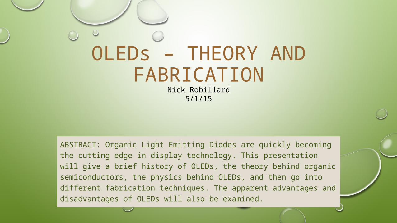
OLEDs – THEORY AND FABRICATION
ABSTRACT: Organic Light Emitting Diodes are quickly becoming the
cutting edge in display technology. This presentation will give a brief history
of OLEDs, the theory behind organic semiconductors, the physics behind
OLEDs, and then go into different fabrication techniques. The apparent
advantages and disadvantages of OLEDs will also be examined.
Nick Robillard5/1/15
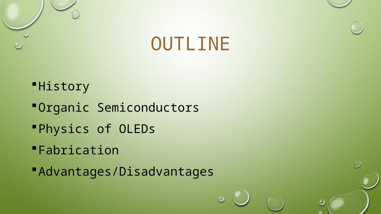
OUTLINE
History
Organic Semiconductors
Physics of OLEDs
Fabrication
Advantages/Disadvantages
HISTORY OF OLEDs
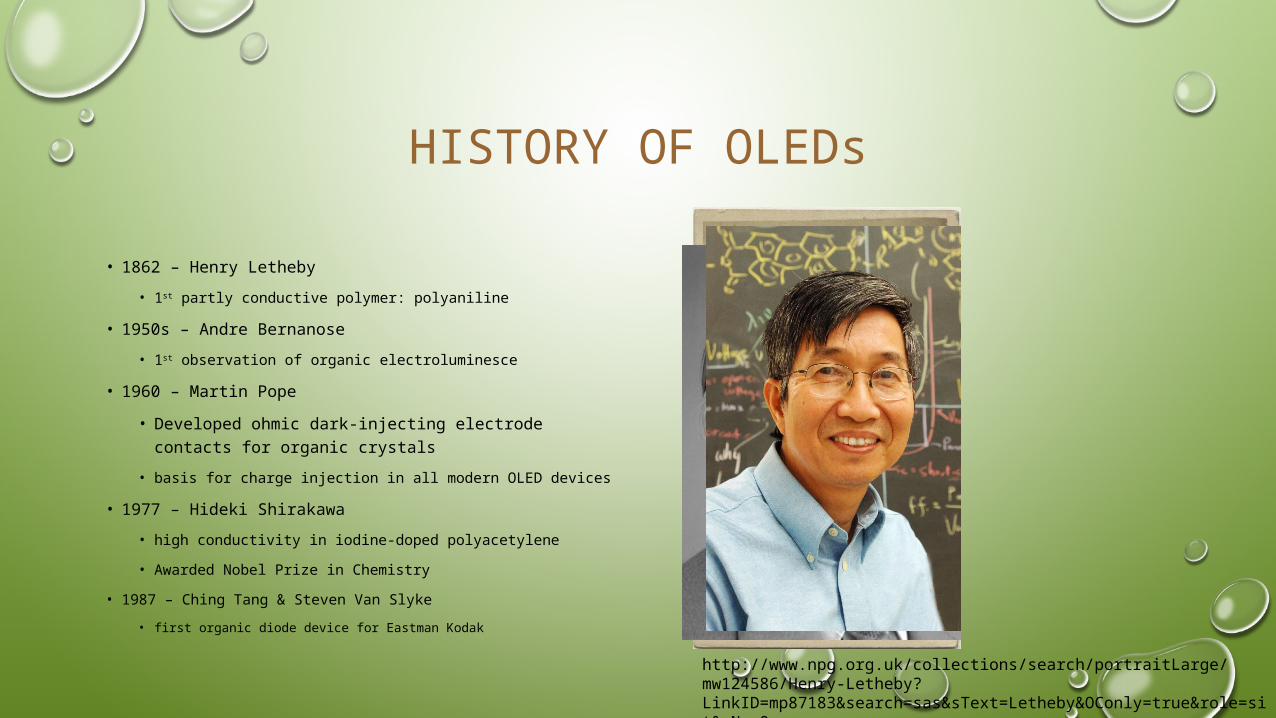
• 1862 – Henry Letheby
• 1st partly conductive polymer: polyaniline
• 1950s – Andre Bernanose
• 1st observation of organic electroluminesce
• 1960 – Martin Pope
• Developed ohmic dark-injecting electrode contacts for organic crystals
• basis for charge injection in all modern OLED devices
• 1977 – Hideki Shirakawa
• high conductivity in iodine-doped polyacetylene
• Awarded Nobel Prize in Chemistry
• 1987 – Ching Tang & Steven Van Slyke
• first organic diode device for Eastman Kodakhttp://www.npg.org.uk/collections/search/portraitLarge/mw124586/Henry-Letheby?LinkID=mp87183&search=sas&sText=Letheby&OConly=true&role=sit&rNo=0
History of OLEDs(cont)
• 1990 – JH Burroughs
• High efficiency green light emitting polymers
• Sheets 100 nm thick
• 1998 – Kodak & Sanyo
• Full-Color AMOLED
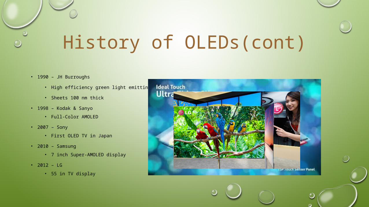
• 2007 – Sony
• First OLED TV in Japan
• 2010 – Samsung
• 7 inch Super-AMOLED display
• 2012 – LG
• 55 in TV display
Organic Semiconductors
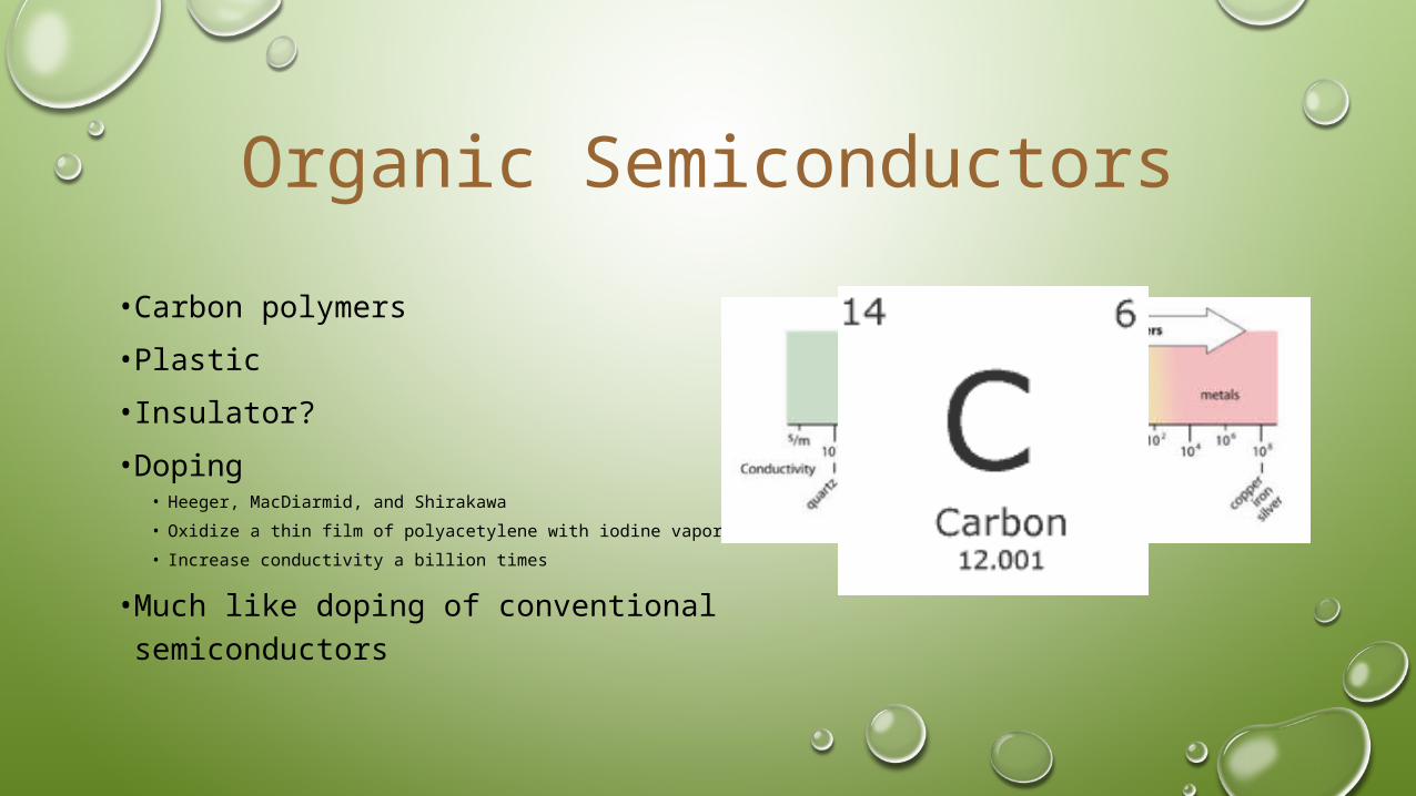
• Carbon polymers
• Plastic
• Insulator?
• Doping• Heeger, MacDiarmid, and Shirakawa
• Oxidize a thin film of polyacetylene with iodine vapor
• Increase conductivity a billion times
• Much like doping of conventional semiconductors
ORGANIC SEMICONDUCTORS(cont.)
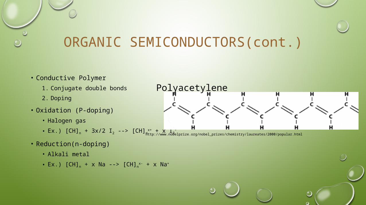
• Conductive Polymer
1. Conjugate double bonds
2. Doping
• Oxidation (P-doping)
• Halogen gas
• Ex.) [CH]n + 3x/2 I2 --> [CH]nx+ + x I3-
• Reduction(n-doping)
• Alkali metal
• Ex.) [CH]n + x Na --> [CH]nx- + x Na+
Polyacetylene
http://www.nobelprize.org/nobel_prizes/chemistry/laureates/2000/popular.html
π and σ Bonds
Organic Semiconductors(cont.)
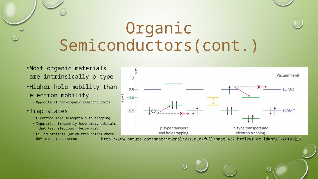
• Most organic materials are intrinsically p-type
• Higher hole mobility than electron mobility
• Opposite of non-organic semiconductors
• Trap states• Electrons more susceptible to trapping
• Impurities frequently have empty orbitals (that trap electrons) below -3eV
• Filled orbitals (which trap holes) above -5eV are not as common
http://www.nature.com/nmat/journal/v11/n10/full/nmat3427.html?WT.ec_id=NMAT-201210
Physics of OLEDs
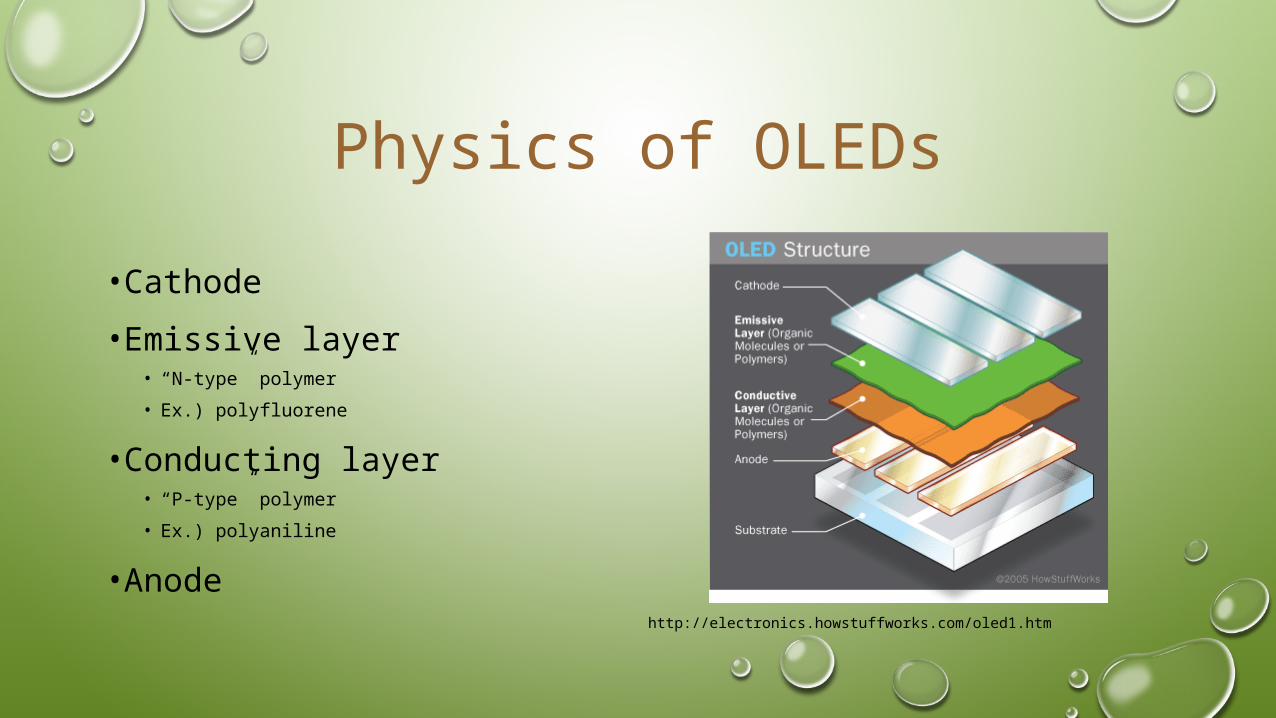
• Cathode
• Emissive layer• “N-type” polymer
• Ex.) polyfluorene
• Conducting layer• “P-type” polymer
• Ex.) polyaniline
• Anodehttp://electronics.howstuffworks.com/oled1.htm
Physics of OLEDs(cont.)
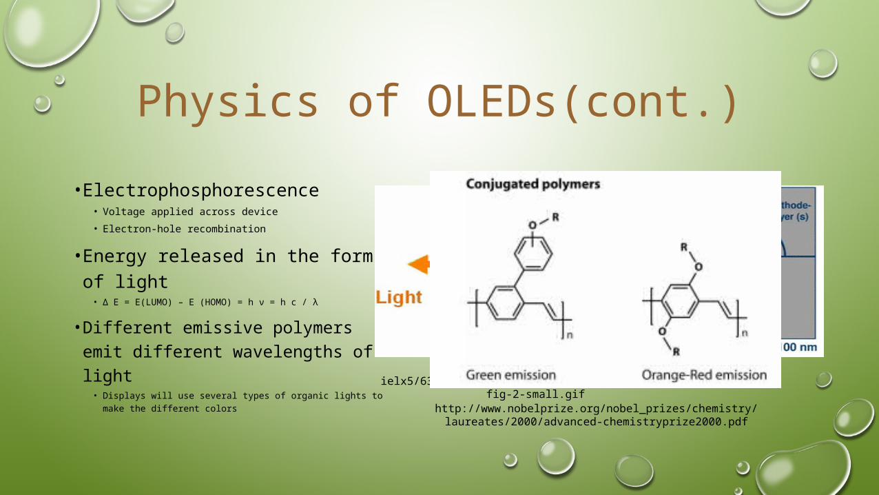
• Electrophosphorescence• Voltage applied across device
• Electron-hole recombination
• Energy released in the form of light
• ∆ E = E(LUMO) – E (HOMO) = h ν = h c / λ
• Different emissive polymers emit different wavelengths of light
• Displays will use several types of organic lights to make the different colors
http://ieeexplore.ieee.org/ielx5/6329165/6338451/6338465/html/img/6338465-fig-
2-small.gifhttp://www.nobelprize.org/nobel_prizes/chemistry/laureates/2000/
advanced-chemistryprize2000.pdf
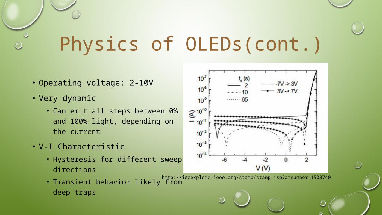
Physics of OLEDs(cont.)
• Operating voltage: 2-10V
• Very dynamic
• Can emit all steps between 0% and 100% light, depending on the current
• V-I Characteristic
• Hysteresis for different sweep directions
• Transient behavior likely from deep traps
http://ieeexplore.ieee.org/stamp/stamp.jsp?arnumber=1503740
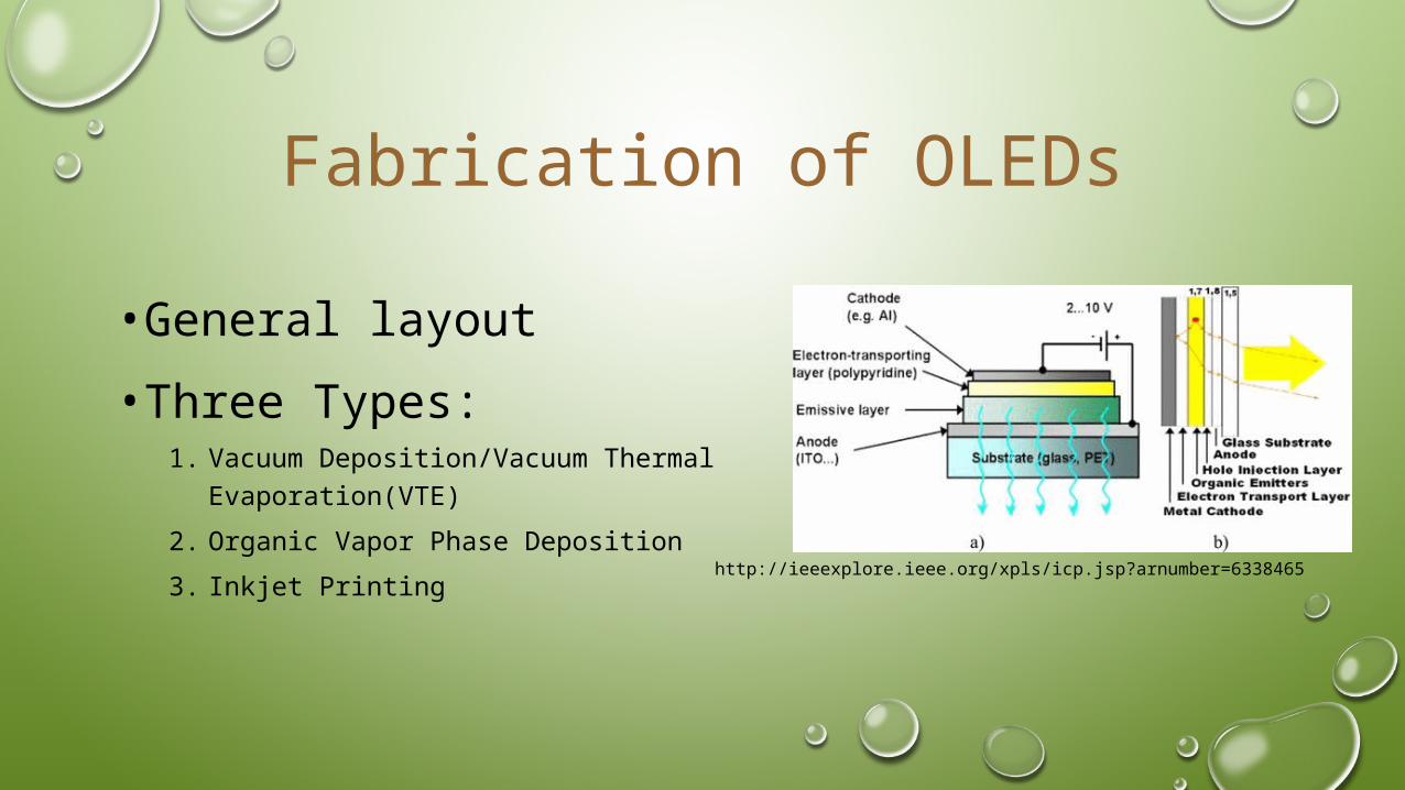
Fabrication of OLEDs
• General layout
• Three Types:1. Vacuum Deposition/Vacuum Thermal
Evaporation(VTE)
2. Organic Vapor Phase Deposition
3. Inkjet Printinghttp://ieeexplore.ieee.org/xpls/icp.jsp?arnumber=6338465
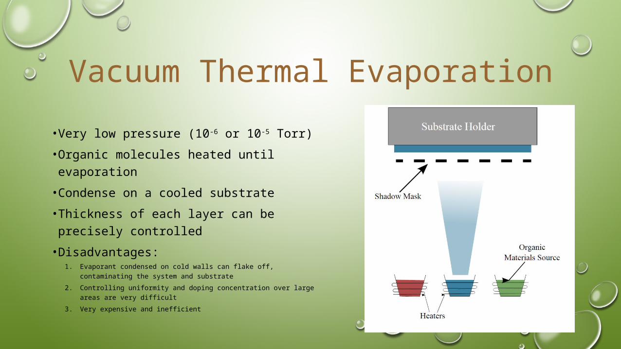
Vacuum Thermal Evaporation
• Very low pressure (10-6 or 10-5 Torr)
• Organic molecules heated until evaporation
• Condense on a cooled substrate
• Thickness of each layer can be precisely controlled
• Disadvantages:1. Evaporant condensed on cold walls can flake off, contaminating
the system and substrate
2. Controlling uniformity and doping concentration over large areas are very difficult
3. Very expensive and inefficient
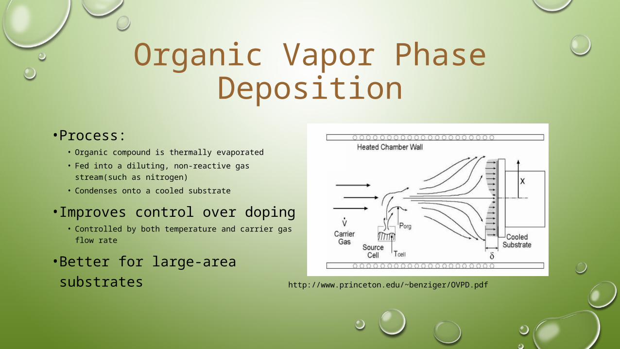
Organic Vapor Phase Deposition
• Process:• Organic compound is thermally evaporated
• Fed into a diluting, non-reactive gas stream(such as nitrogen)
• Condenses onto a cooled substrate
• Improves control over doping• Controlled by both temperature and carrier gas flow
rate
• Better for large-area substrateshttp://www.princeton.edu/~benziger/OVPD.pdf
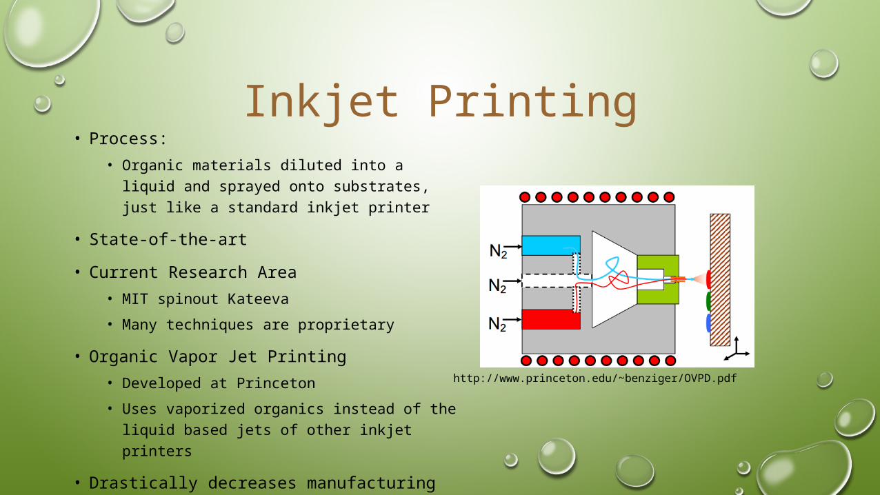
Inkjet Printing• Process:
• Organic materials diluted into a liquid and sprayed onto substrates, just like a standard inkjet printer
• State-of-the-art
• Current Research Area
• MIT spinout Kateeva
• Many techniques are proprietary
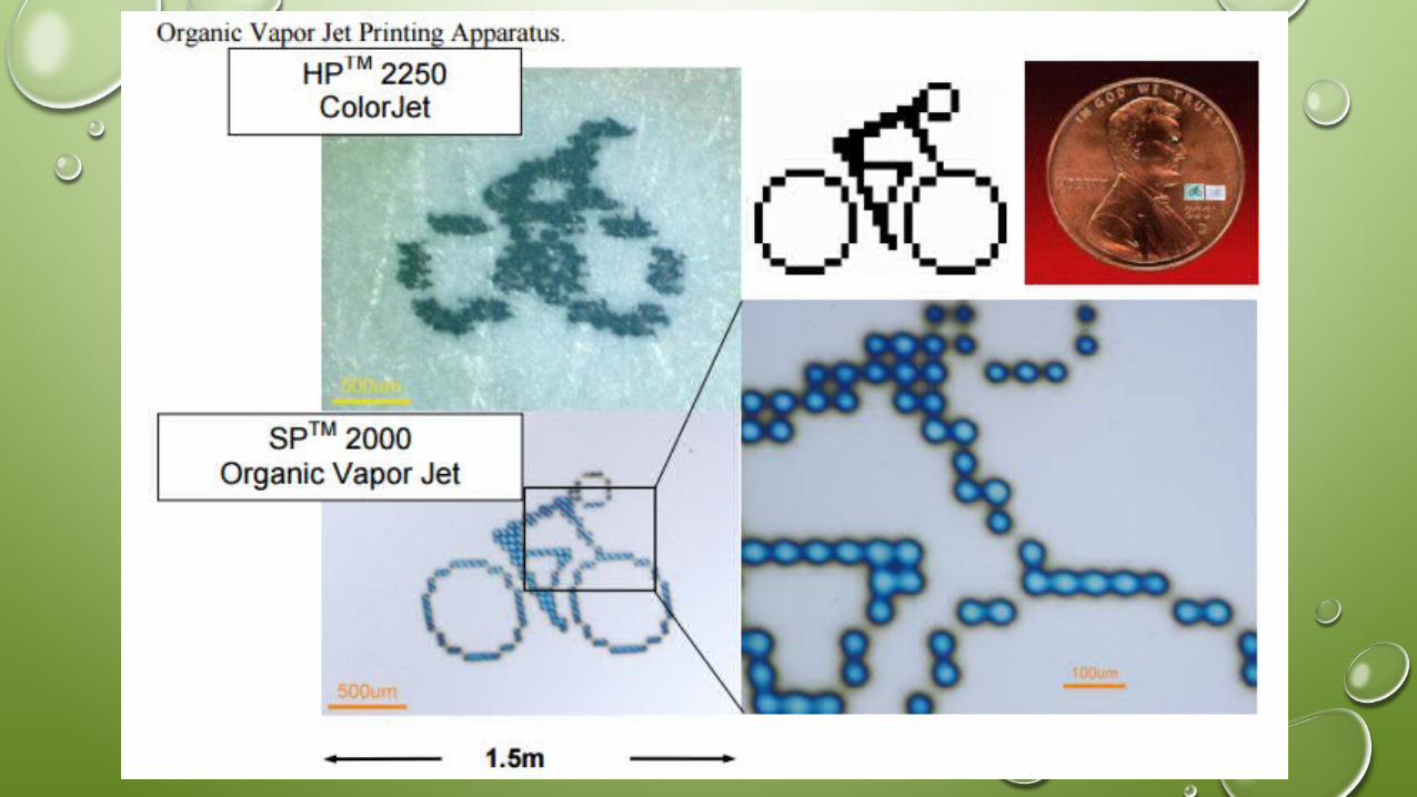
• Organic Vapor Jet Printing
• Developed at Princeton
• Uses vaporized organics instead of the liquid based jets of other inkjet printers
• Drastically decreases manufacturing costs and paves the way for flexible and large-screen models
http://www.princeton.edu/~benziger/OVPD.pdf
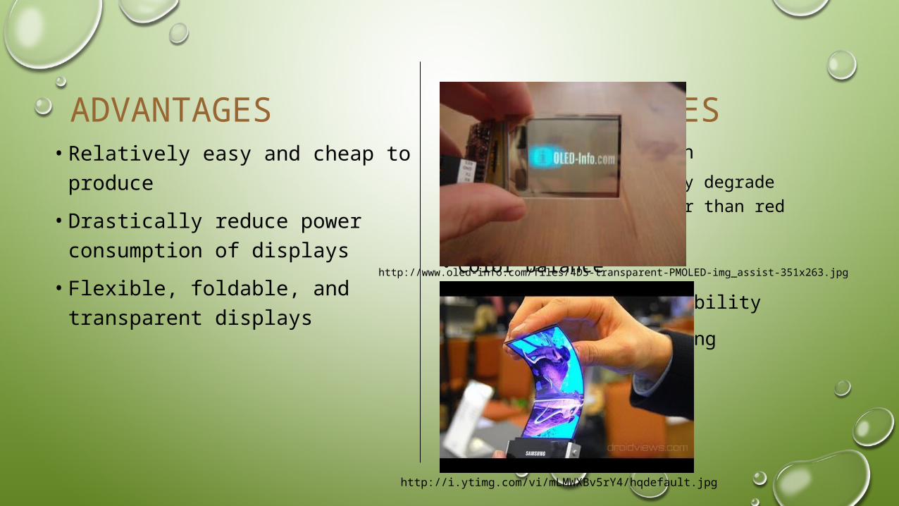
ADVANTAGES• Relatively easy and cheap to
produce
• Drastically reduce power consumption of displays
• Flexible, foldable, and transparent displays
DISADVANTAGES• Questionable lifespan
• Blue OLEDs currently degrade significantly faster than red and green
• Color balance
• Water damage susceptibility
• Expensive manufacturing
http://www.oled-info.com/files/4DS-transparent-PMOLED-img_assist-351x263.jpg
http://i.ytimg.com/vi/mLMWXBv5rY4/hqdefault.jpg
Summary
• OLEDs are made of organic semiconductors
• Discovered by accident by Hideki Shirakawa
• Conjugated Bonds and Doping
• Physics of Electrophosphorescence
• Fabrication• Vacuum Thermal Deposition
• Organic Vapor Phase Deposition
• Inkjet Printing
• Advantages/Disadvantages
References
• http://newsoffice.mit.edu/2015/mass-produced-inkjet-printed-oled-displays-0212
• http://www.princeton.edu/~benziger/OVPD.pdf
• http://ieeexplore.ieee.org.libpdb.d.umn.edu:2048/stamp/stamp.jsp?tp=&arnumber=1511521
•
http://electronics.howstuffworks.com/oled7.htm
•
http://spectrum.ieee.org/tech-talk/semiconductors/materials/organic-glasses
•
http://spectrum.ieee.org/semiconductors/materials/organic-semiconductor-breakthrough-could-speed-flexible-circuits
•
http://www.nobelprize.org/nobel_prizes/chemistry/laureates/2000/popular.html
References(cont.)
• http://www.nobelprize.org/nobel_prizes/chemistry/laureates/2000/advanced-chemistryprize2000.pdf
•
http://www.nature.com/nmat/journal/v11/n10/full/nmat3427.html
•
http://ieeexplore.ieee.org/stamp/stamp.jsp?arnumber=1503740
•
http://ieeexplore.ieee.org/xpls/icp.jsp?arnumber=973248
• http://en.wikipedia.org/wiki/Organic_semiconductor
• http://en.wikipedia.org/wiki/OLED
Questions/Comments?