Embed Size (px)
Citation preview

Resist TWG, EUV Symposium October 2011
NXE resist outgas testing update
Noreen Harned20 October 2011

Slide 2 Resist TWG, EUV Symposium October 2011
Resist outgassing can impact scanner performance if not managed
Carbon growth on mirrors from outgassing depends on the outgas rate and pressure and gas transport and intensity at the mirrorsOutgas requirements have been set to maintain the system performance over the expected system lifetime productivityOutgassing from resist – cleanable and non-cleanable –has been given an allocation in the transmission budget Testing of resists for compliance with outgas requirements must mimic the scanner for environment, cleaning and contamination regime
Resist outgas tester requirements have been determined based on this

Slide 3 Resist TWG, EUV Symposium October 2011
Resist outgassing reuirements have been allocated to maintain optics reflectivity
Cleanable contamination:NXE optics cleaning system is designed to maintain high productivity over a target lifetime such that had there not been cleaning a large amount of carbon (C) would build up per mirrorFilm thickness has been given a direct allocation from the budget
Non cleanable contamination:Total change in transmission ≤10% for the optical column over the lifetime (~1% reflection loss per mirror) is requiredAllocations for the 1% dR/R are made for coating degradation, sputtering, cleaning residual, oxidation, cleaning by-products (eg metal from filament, outgassingfrom use of cleaning baths) and resist For HVM the budget allocated for resist is allocated dR/R of ≤0.16%

Slide 4 Resist TWG, EUV Symposium October 2011
Presentation contents
Resist outgas tool process flow, requirements, resultsUse of electrons and correlation to photonsTester status for NXE qualification

Slide 5 Resist TWG, EUV Symposium October 2011
Resist Qualification has four main steps
Ellipsometry XPS
H2
H•H•H•
1 2 3Grow
contaminationMeasure
contamination film thickness
Cleancontamination
Measure non-cleanedcontamination
4
Tester H* Filament
•
Ellipsometry
measurements allow qualification of cleanable contamination
•
XPS measurements allow qualification of uncleanable contamination
•
Uncleanable contamination is the biggest concern for optics lifetime
Slide 6 Resist TWG, EUV Symposium October 2011
Spectroscopic ellipsometer (SE) requirements for dose to clear and total contamination measurement
Measurements on 1” witness samples (for peak contamination measurement) and 12” wafers (dose to clear measurement)2D spectroscopic ellipsometry (wavelength range 300-900nm with Cauchy model, provided by ASML, fit from 600nm – 900nm)125 - 150 µm spot size150 µm raster on a 5 x 5 mm² area
Spectroscopic data Psi (Y) and Delta (D) is obtainedDetection limit/accuracy 0.1nm/±0.1nmCross-calibration to ASML metrology (measure and compare) to check for 10% matching
ASML supplied witness sample with uniform carbon or SiO2ASML supplied witness sample with grown contamination peak

Slide 7 Resist TWG, EUV Symposium October 2011
XPS requirements for non-cleanable contamination measurement
Measurements on 1” witness samplesAccuracy / detection limit 0.1 %at and repeatability ≤ 10%Monochromatic Al Kα radiation sourceSpot size 500 µm or smaller Angle set to reach the preferred information depth of 8 - 10nm on SiO2 (Take off angle 90 deg 10nm; TOA 51 deg 8nm)Cross-calibration with reference sample provided by ASML (measure and compare) for 1.5 at% matching (except Ru, O, N)
ASML supplied witness sample that has been cleaned after contamination was grown (no splitting of Ru / C peaks needed)
#176 Center Measurement Atomic Percentage (%)
Peak S 2p W 4d5 P 2p Ru 3d O 1s N 1s Zn 2p3 Si 2sOther 3.4 0.2 1.0 46.7 42.0 5.8 0.1 0.6
MiPlaza 3.1 0.3 1.2 47.1 42.1 5.7 0.1 0.3

Slide 8 Resist TWG, EUV Symposium October 2011
Resist outgassing specifications have been set for NXE3100 and NXE3300
Outgassing specifications are based onCleanable contamination can be removed within the availability budgetMaximum transmission loss from uncleanable contamination of 10% during 30,000h EUV exposures
The NXE3100 specifications have been revised to take into account the current tool status and expected tool lifetime
All resists that pass the NXE3100 requirement can be used without wafer count restriction
Cleanable (C thickness) Uncleanable (dR/R)NXE:3100 3nm 0.23%NXE:3300 3nm 0.16%

Slide 9 Resist TWG, EUV Symposium October 2011
With the relaxed NXE3100 specification all resists tested by ASML can be used without restriction
dr/r (%)Resist 1Resist 2Resist 3Resist 4Resist 5Resist 6Resist 7Resist 8Resist 9Resist 10Resist 11Resist 12Resist 13Resist 14Resist 15Resist 16Resist 17Resist 18Resist 19Resist 20Resist 21Resist 22Resist 23Resist 24Resist 25Resist 26
All resists tested meet the cleanables requirementAll resists meet the revised NXE 3100 non-cleanables requirement9 of 26 resists tested meet the NXE3300 requirement
Failure mostly due to S content
Resist suppliers have been notified as to Pass / Fail of their resists that have been tested
Results have been shown to be repeatable to 10%
dr/r (%)Resist 1Resist 2Resist 3Resist 4Resist 5Resist 6Resist 7Resist 8Resist 9Resist 10Resist 11Resist 12Resist 13Resist 14Resist 15Resist 16Resist 17Resist 18Resist 19Resist 20Resist 21Resist 22Resist 23Resist 24Resist 25Resist 26
NXE3100 NXE3300

Slide 10 Resist TWG, EUV Symposium October 2011
Presentation contents
Resist outgas tool process flow, requirements, resultsUse of electrons and correlation to photonsTester status for NXE qualification

Slide 11 Resist TWG, EUV Symposium October 2011
Tester requirements [1 of 2]Item Specification
1 System performance
a Pumping speed < 265 l/s
b Vacuum quality checked multiple days Ptotal
< 1.5 x 10⁻⁷
mbar
c Transfer time wafer1 < 15 min
d Transfer time WS1 < 15 min
e Wafer e-gun or photon stability over 2 hrs < 5%
f WS e-gun or photon stability over 2 hrs < 5%
2 Dose to Clear
a Repeatability2 <6%
b Total test time < 60 min
1Productivity items 2Resist coating uniformity (1.5nm) and repro (60nm ± 3nm) required

Slide 12 Resist TWG, EUV Symposium October 2011
Tester and cleaner requirements [2 of 2]Item Requirement
3 Contamination growth3
a Repeatability4 <10%
b Background contribution <0.3 nm
c Contamination growth regime Contamination limited
d Total test time1 < 90 min
e Repeatability non cleanable <25%
f Background contribution non-cleanable (S, SOx) ≤0.1 at%
4 Cleaning
a Filament temperature 1800 oC
< T ≤2000 oC
b Sample temperature ≤ 60 oC
cBackground contribution to non-cleanables (S, SOx)
Background contribution to non-cleanables (Sn,W, Zn)≤
0.6 at%±0.2 at%< 1.0 at%
d Cleaning rate1 >10 nm/h
e Cleaning time1 < 60 min1Productivity items 3Tested for both fast and slow resist 4Nominal wafer expose 60 min
Slide 13 Resist TWG, EUV Symposium October 2011
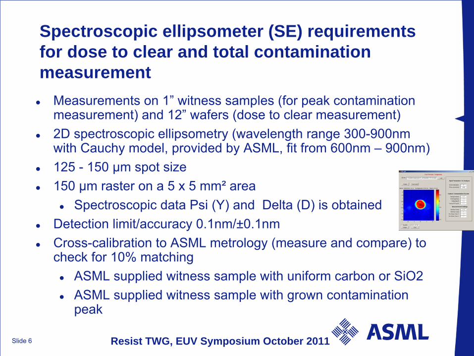
E-beam test enables fast and low cost resist screening
Streaming resist-coated Cu tape
Witnes
s mirror
M1
Witness mirror M2
“Cx Hy :R” EUV light
E-gun advantages over photon testingAbundant intensity means contamination can be grown quicklySingle wafer exposure therefore small amounts of resist is neededEasier maintenance (no EUV source)

Slide 14 Resist TWG, EUV Symposium October 2011
Resist outgassing is caused by secondary electrons from either photons or electrons
Photons travel through the resist, are absorbed, and create secondary electrons originating from the molecules of the substrate material
This triggers an avalanche of secondary electrons which in turn causes the resist decomposition and outgas
Electrons are not absorbed but loose their energy by multiple collisions in the resist
This also creates an avalanche of secondary electrons which movethrough the resist which causes the decomposition and outgas
Secondary electron emission has been studied extensively and the energy distribution for both photon and electron induced secondary emission from a Si substrate has the same shape and differs primarily in the number of secondary electrons producedYield determines the number of secondary electrons and thus dose calibration, with electrons, is an important part of the testing to be sure that exposure is nominally at Eo
Dose to clear testing is done for each resist
Slide 15 Resist TWG, EUV Symposium October 2011
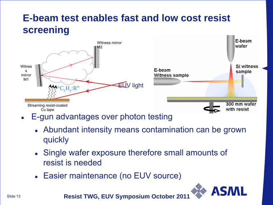
E-beam energy at wafer is selected to match EUV photons in resist
Electron trajectories are simulated using the screened Rutherford elastic cross sectionEnergy spectrum of the secondary electrons mostly depends on the emitting material but not on the type or energy of the particlesOnly minor part of EUV photons are absorbed by resistTo match EUV exposure, a minimum e-beam energy of 2keV is required
1 keV 2 keV 5 keVPrimary electron trajectories with beam energy
60 nmresist
1o electron beam
Electrons do notreach bottom ofresist

Slide 16 Resist TWG, EUV Symposium October 2011
Fit for calibration resists is excellent regardless of the use of photons or electrons
R^2 NIST LTJ SAT CNSE ASMLNIST 1 0.93 0.91 0.88
LTJ SAT 0.93 1 1.00 0.99CNSE 0.91 1.00 1 1.00ASML 0.88 0.99 1.00 1
Both electrons and photons give similar results for resist exposureKey things that enable the good match are
Selection of e-gun energyTester cleanliness and geometryIntensity at the WSGood process control and metrology
Wafer / WS P/P E/E P/E E/E
P = Photons E = Electrons

Slide 17 Resist TWG, EUV Symposium October 2011
Calibration curves have been made for each set up
Photon Data versus CNSE E-Beam Data
y = 1.5382xR2 = 0.685
0.0
1.0
2.0
3.0
4.0
5.0
6.0
7.0
8.0
0.0 1.0 2.0 3.0 4.0 5.0Photon induced contamination (nm)
CN
SE e
lect
ron
indu
ced
cont
amin
atio
n (n
m)
Photon Data versus SEC E-Beam Data
y = 3.3908xR2 = 0.7865
0.0
2.0
4.0
6.0
8.0
10.0
12.0
0.0 1.0 2.0 3.0 4.0 5.0Photon induced contamination (nm)
SEC
ele
ctro
n in
duce
d co
ntam
inat
ion
(nm
)Linear fit for different resists is very goodCalibration curve accounts for differences in processing, metrology and tester variation

Slide 18 Resist TWG, EUV Symposium October 2011
Presentation contents
Resist outgas tool process flow, requirements, resultsUse of electrons and correlation to photonsTester status for NXE qualification

Slide 19 Resist TWG, EUV Symposium October 2011
Summary status for resist outgas testing
NIST, the end user of the first LTJ system, and CNSE have completed all of the qualification steps and are ready to test resists for compliance with NXE specificationsIMEC continues to work on their plan towards completion this year and have completed several key stepsTest report template has been shared with all who are doing testing and all who might receive test result reports, including all resist suppliers (see last sheet for points of contact at resist suppliers)

Slide 20 Resist TWG, EUV Symposium October 2011
Data package check list for tester qualification
Data package Data description1 Facilities a Specification resist processing (uniformity and repro)
b Specification ellipsometerc Ellipsometry C or SiO2 on Si sample (fixed thickness cross ref)d Ellipsometry Si/Ru/C peak samplee Specification XPSf XPS Si / Ru / cleaned contamination ASML refence sample
2 Vacuum a RGA spectrum of ultra clean vacuum with pressure readingb Pumping speed data of calibration mixture
Functionality a Witness sample e-beam stability datab Wafer e-beam or photon stability data
3 Cleaning a Cleaning process conditionsb Sample temperature profile as a results of duty cyclec Cleaning background contribution
4 Qualification tests a Contrast curve of specified resist to determine D2Cb D2C exposure W2W reproducibilityc D2C exposure within wafer uniformityd Exposed area and test timing contamination growth teste Reproducibilty of contamination growth exposuref Contamination grown from background (total thickness)g Contamination grown from background (content)
5 Calibration a Check outgassing limited contamination growth regimeb Calibration exposures (3 - 4 resists)

Slide 21 Resist TWG, EUV Symposium October 2011
Status of systems in qualification for NXE resist testing
In processDone NOKPlanned
Data package Data description LTJ SAT CNSE NIST IMEC1 Facilities a Specification resist processing (uniformity and repro)
b Specification ellipsometerc Ellipsometry C or SiO2 on Si sample (fixed thickness cross ref)d Ellipsometry Si/Ru/C peak samplee Specification XPSf XPS 3-layer sample (SiN/TiN/SiN)g XPS Si / Ru / cleaned contamination ASML refence sample
2 Vacuum a RGA spectrum of ultra clean vacuum with pressure readingb Pumping speed data of calibration mixture
Functionality a Witness sample e-beam stability datab Wafer e-beam or photon stability data
3 Cleaning a Cleaning process conditionsb Sample temperature profile as a result of duty cyclec Cleaning background contribution
4 Qualification tests a Contrast curve of specified resist to determine D2Cb D2C exposure W2W reproducibilityc D2C exposure within wafer uniformityd Exposed area and test timing contamination growth teste Reproducibilty of contamination growth exposuref Contamination grown from background (total thickness)g Contamination grown from background (content)
5 Calibration a Check outgassing limited contamination growth Japanb Calibration exposures (3 - 4 resists)
Not applicable
Slide 22 Resist TWG, EUV Symposium October 2011
Show test report template


![Stochastic modeling of EUV resists: simulation of the ...ieuvi.org/TWG/Resist/2016/20161023/09_biafore_kt.pdf · 10/23/2016 · [2] A. Reiser, ‘Photoreactive Polymers,’ Wiley,](https://img.dokumen.tips/doc/110x75/5fd7f431b79d9c0e3b4c13df/stochastic-modeling-of-euv-resists-simulation-of-the-ieuviorgtwgresist20162016102309biaforektpdf.jpg)