Embed Size (px)
Citation preview

Transworld Research Network 37/661 (2), Fort P.O., Trivandrum-695 023, Kerala, India
Semiconductor Machining at the Micro-Nano Scale, 2007: ISBN: 978-81-7895-301-4 Editors: Jiwang Yan and John Patten
2 Numerical simulations and cutting experiments on single point diamond machining of semiconductors and ceramics
John A. Patten1, Jerry Jacob1, Biswarup Bhattacharya1 Andrew Grevstad2, Ning Fang3 and Eric R. Marsh4 1Department of Manufacturing Engineering, Western Michigan University Kalamazoo, Michigan; 2Thirdwave Systems, Minneapolis, Minnesota 3Utah State University, Logan, Utah; 4The Pennsylvania State University University Park, Pennsylvania, USA
Abstract This chapter presents numerical simulation work and single-point nano-machining experiments conducted on semiconductor and ceramic materials, e.g. silicon (Si) and silicon carbide (SiC). The apparent ductile mode material removal mechanism observed in these materials is believed to be the result of a high pressure phase transformation (HPPT), which generates a small
Correspondence/Reprint request: Dr. John A. Patten, Department of Manufacturing Engineering, Western Michigan University, Kalamazoo, Michigan, USA. E-mail: [email protected]

John A. Patten et al. 2
plastic zone of material at the tool-work piece contact interface that behaves in a metallic manner. This metallic behavior provides the motivation for using AdvantEdge, a metal machining simulation software, for comparison to experimental results. The first section of this chapter describes numerical simulations of single point diamond turning (SPDT) experiments conducted on single crystal 6-H SiC. The SPDT experiments have shown ductile chip formation similar to that seen in the machining of metals. The cutting and thrust forces generated from the experiments under ductile cutting conditions compare favorably with the machining simulation results. As the depth of cut is decreased (from 250 nm to 100 nm down to 50 nm) the material removal mechanism transitions from brittle to a ductile response, with the 50 nm cuts being dominated by ductile events. Thus the forces from the experiment and the simulations are in much better agreement for the smaller depths of cut, i.e. below the critical depth of cut that establishes the ductile to brittle transition (DBT), as ductile conditions exist in both the simulation and experiments. The differences in the results are due to elastic deformation under the tool leading to increased rubbing at small depths of cut, and the occurrence of brittle behavior for the experimental results at the largest depths of cut. The first section of this chapter also presents a predictive analytical model for machining with a large negative rake angle tool, the condition which is very common in nano machining. The second section presents results from a fly-cutting experiment conducted on single crystal 6H-SiC. The cutting tests were performed to determine the critical depth of cut (for ductile to brittle transition), while machining on the (0001) face. The cuts were made using a single crystal synthetic diamond tool with a -45° rake angle and a 1 mm nose radius at a speed of 82.5 mm/sec. A scanning white light interferometric microscope (Wyko RST) is used to detect the ductile to brittle transition of SiC based on the surface topography of the cut surfaces. For each individual cut, the cutting and thrust forces are correlated to the resulting depths along the cut, to determine the chip cross-sectional areas. This information is then used to normalize the force values, which effectively eliminates variations in force due to problems with workpiece flatness while machining. An estimate of the friction factor due to interaction of the SiC and diamond tool is also obtained. The third section presents 3-D numerical simulation work relating to scratching experiments conducted on both Si and SiC with a stylus-radius diamond tip. These experiments were also aimed at determining the DBT depth in these materials. The simulations were conducted at the different depths and the cutting and thrust forces were compared to experimental

Simulations and machining experiments on ceramics 3
results. The initial attempt at simulation of scratching in 3-D shows promising results. Introduction
The mechanical and thermal properties of silicon carbide (SiC) have traditionally allowed for its use in refractory linings and heating elements for industrial furnaces, as an abrasive in manufacturing processes, and in wear resistant parts in rotating machinery such as pumps and engines. There is currently growing interest in the use of SiC in the optics industry for space based laser mirrors, as a replacement for beryllium. Also in the electronics industry SiC is being used for high-powered/high temperature devices, where its high thermal conductivity, high electric field breakdown strength, and high maximum current density make it more promising than silicon (Si) [1]. The successful acceptance of SiC in these industries will require satisfaction of stringent requirements on form accuracy and sub-surface damage [2] where surface finishes better than 10 nm are considered standard specifications [3].
Brittle mode grinding and chemical-mechanical polishing (CMP) have been used to meet product requirements and manufacturing productivity. Since grinding and polishing are slow and costly there is a continuing motivation to use SPDT to eliminate some of these steps [2] to reduce production time and to reduce overall component costs. Additionally, traditional grinding induces micro-cracks in the surface of brittle materials [4], while polishing is required to then remove the surface and subsurface damage caused by grinding [2].
Ductile mode machining or cutting technology has been studied as a replacement for grinding of optical devices and semiconductors, such as Si [2, 4]. The machining of this hard and brittle material is presumed to be made possible due to the ductility, and presumed metallic nature, of its high pressure phase (HPP), or possibly as a result of amorphization [15]. The tremendous hydrostatic pressure and shear stress in the region immediately surrounding the tool cutting edge allows materials like Si and also SiC to behave in a ductile fashion at small depths of cut, exhibiting plastic deformation at room temperatures [6].
The ability to characterize the mode of material removal through simulations provides an alternative approach to understanding the effect of varying machining parameters, such as rake angle, cutting edge radius, and depth of cut. A comparison of the resultant force per unit cross-sectional chip area (expressed as a pressure in GPa) can provide a measure or an indication of the mode of material removal, i.e. ductile or brittle.

John A. Patten et al. 4
1. Comparison between numerical simulations, cutting experiments and an analytical model for single point diamond turning of single crystal silicon carbide 1.1 Background Experiments conducted in recent years on Si [2, 4] and silicon nitride [5] have demonstrated a ductile mode of material removal similar to that seen in metals. Ductile mode implies a process dominated by ductile or plastic material deformation and removal rather than brittle fracture, resulting in a smooth surface (similar to a polished surface) free of fracture damage [7]. The ductile nature of these hard and brittle materials has been attributed to the HPPT, which occur at or near room temperature. The HPPT is created as a result of the contact between the sharp tool and the workpiece at or below the critical depth of cut [6]. This critical depth has been demonstrated to be in the nanometer range for SiC [2, 5, 6, 7]. Recent work [7] involving Single Point Diamond Turning (SPDT) of single crystal SiC was conducted to study, among other things, the effect of varying the rake angle and the depth of cut on the cutting and thrust forces, the resultant surface finish and the ductile to brittle transition (DBT). The forces from the experiment directly indicate whether the material removal is ductile or brittle during processing, while the final surface finish roughness indicates the achievement of ductile or brittle material removal. Ductile machining is characterized by higher cutting forces, as it takes more energy to remove material in a ductile mode as opposed to brittle material removal for the same volume of material [7]. The focus of this section is to determine and evaluate the capability and accuracy of predicting the experimental results in the work reported in [7] based on 2-D turning simulations conducted using version 4.5 of the commercial machining simulation software AdvantEdge. 1.2 Experimental procedures and conditions Results from three sets of experiments on single crystal SiC are considered for comparison to the simulations. The first set of experiments involved depths of cut (in-feed) of 100 nm, 300 nm and 500 nm using a 2 mm round nose mono-crystalline diamond tool with a 0° rake angle. This same tool was reoriented to create an effective rake angle of -45°, and cuts were made at the same depths forming the second set of experiments. The first two sets of experimental results are reported in [7]. Additionally, machining at a depth of 50 nm was conducted but not reported previously. The third set of experiments involved 50 nm and 250 nm depths using a flat nose mono-crystalline diamond tool with a -45º rake angle. The experiments were all conducted at a low speed
Simulations and machining experiments on ceramics 5
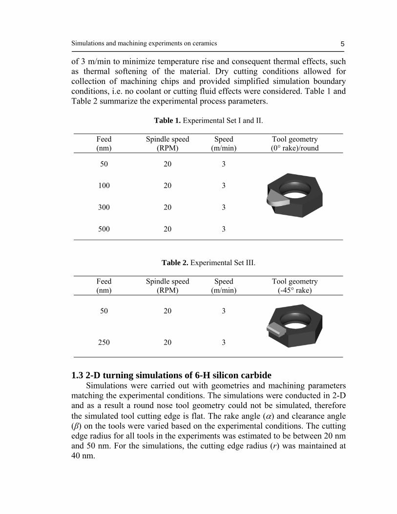
of 3 m/min to minimize temperature rise and consequent thermal effects, such as thermal softening of the material. Dry cutting conditions allowed for collection of machining chips and provided simplified simulation boundary conditions, i.e. no coolant or cutting fluid effects were considered. Table 1 and Table 2 summarize the experimental process parameters.
Table 1. Experimental Set I and II.
Feed (nm)
Spindle speed (RPM)
Speed (m/min)
Tool geometry (0° rake)/round
50 20 3
100 20 3
300 20 3
500 20 3
Table 2. Experimental Set III.
Feed (nm)
Spindle speed (RPM)
Speed (m/min)
Tool geometry (-45° rake)
50 20 3
250 20 3
1.3 2-D turning simulations of 6-H silicon carbide Simulations were carried out with geometries and machining parameters matching the experimental conditions. The simulations were conducted in 2-D and as a result a round nose tool geometry could not be simulated, therefore the simulated tool cutting edge is flat. The rake angle (α) and clearance angle (β) on the tools were varied based on the experimental conditions. The cutting edge radius for all tools in the experiments was estimated to be between 20 nm and 50 nm. For the simulations, the cutting edge radius (r) was maintained at 40 nm.

John A. Patten et al. 6
The simulation process is a 2-D Lagrangian finite element-based machining model assuming plane strain conditions [8]. A typical setup for 2-D orthogonal turning with relevant parameters is shown in Table 3. Note that the nose radius cannot be simulated in 2-D but the approximation is valid for the small feeds for which the experiment and simulation were conducted. The workpiece was made long enough to ensure that the length of cut (loc) along the workpiece would allow for steady state conditions to be achieved. The height (h) of the workpiece was much larger (between 10 to 100 times) in comparison to the feed or uncut chip thickness. The boundary conditions of the workpiece surface is assumed to be traction free and constrained in the vertical direction. The top and rear surfaces of the tool are rigidly fixed with adiabatic conditions.
Table 3. Parameter listing for 2-D turning.
Variable Variable Definition Workpiece-Tool geometry
r tool cutting edge radius
α tool rake angle
β tool clearance angle
Feed, f In-feed/uncut chip thickness
loc length of cut
v work piece velocity
h height of workpiece
The simulations were carried out using elastic properties for a 6H-SiC polycrystalline material model, although the experiment made use of a single crystal 6H-SiC wafer, thus no crystal orientation effects (planes and directions) were included in the simulations. Additionally, the material model was set up to simulate a ductile workpiece, i.e. similar to metal machining. The material model for the tool is polycrystalline diamond with elastic properties. To reflect the ductile behavior in ceramics created by the HPPT, a pressure sensitive Drucker-Prager constitutive model as proposed by [5] was specified. The Drucker-Prager yield criterion is given by
3 J2⋅ I1 α⋅+ κ− 0= (1)
where I1 is the first invariant of the stress tensor, J2 is the second invariant of the deviatoric stress tensor, α is the pressure sensitivity coefficient, and κ is a material constant.

Simulations and machining experiments on ceramics 7
The quantity J2 is given by
J216
σ1 σ2−( )2 σ2 σ3−( )2+ σ3 σ1−( )2+⎡⎣
⎤⎦=
(2)
where σi are the principal stresses. The quantity κ is given by
κ2 σt σcσt σc+
=
(3) which is equal to the yield stress in the case when σc = σt, i.e. no pressure dependency, and where σt and σc are the yield stress in tension and compression respectively. The hardness of the SiC material is 26 GPa and the initial tensile yield stress is taken to be 11.82 GPa based on a proposed initial yield value of H/2.2 for brittle materials. The compressive yield is set to equal the hardness (H) of the material [5], to reflect the effect of the HPPT For a uniaxial stress state (σ2 and σ3 are zero),
I1 σ1= (4)
J2σ1
2
3=
(5)
Now using Equation 1.3, κ equals 16.25 GPa while α equals -0.375. These parameters are used to provide a pressure-sensitive material model. Brittle fracture behavior is not modeled in this current work. Since a slow cutting speed of 3 m/min was used during machining, the temperature rise was not expected to be significant based on simulations by [9]. As a result, thermal calculations were not enabled for the simulations in the interest of reducing computing time. A coefficient of friction (COF) of 0.4 was specified for the simulation based on the apparent COF from experimental data [16]. The simulation matrix created to match all experimental conditions is given in Table 4.

John A. Patten et al. 8
Table 4. Simulation matrix.
Experimental Set
Depth of cut*, nm
Rake Angle, °
Clearance Angle, °
Tool geometry/(flat nose)
100 0 5
300 0 5 Set I
500 0 5
50 -45 50
100 -45 50
300 -45 50 Set II
500 -45 50
50 -45 5 Set III
250 -45 5
*The depth of cut (doc) here refers to the in-feed or the uncut chip thickness. 1.4 Analysis of force data for different tools In order to make a one-to-one comparison of the forces, the experimental conditions and the simulated conditions need to be considered. To conform to a 2-D orthogonal cut for the experiments, the single crystal wafer of SiC was machined on its circumference (a plunge cut across the full width of its thickness) rather than the polished face. As a result, the only forces generated are cutting forces and thrust forces. Thus, a 2-D simulation of the experimental (machining) conditions is reasonably approximated. Experimental sets I and II made use of a round nose tool, while set III involved the use of a flat nose tool. The simulations were conducted in 2-D and as such, the results are directly comparable to a flat nose tool. A direct comparison of the experimental results and the simulation results for the nose radius tool is still valid. This is because the radius of curvature of the round nose tool (2 mm) used in the experiments, is much larger than the thickness of the wafer (250 µm, i.e. maximum width of the cut) over which the cuts were made (depths less than 500 nm). The experimental cutting force and thrust force data provided in the graphs that follow are obtained from work done by [7]. For comparison to the simulated results, a single value of each force is reported which is representative of the average force for a given depth. However, for each depth, the crystallographic nature of the single crystal material created alternating regions of ductile and

Simulations and machining experiments on ceramics 9
brittle material removal. Thus an averaged ductile force is reported when the machining operation is dominated by ductile material removal, and an averaged brittle force is reported in other cases dominated by brittle material removal. For the simulations, the force results are always for the ductile conditions. 1.4.1 Cutting force and thrust force data for 0° rake angle with 5° clearance angle Figure 1 shows a comparison plot of the cutting forces from the experiments and the simulations for different depths using a 0° rake angle tool with a 5° clearance. The simulation results show a steady increase in the cutting force with an increase in depth. The cutting forces from the experiments, however, do not show this trend. Note that brittle experimental cutting force values, i.e. lower values compared to purely ductile cuts, are reported in the case of 300 nm and 500 nm depths of cut, as these cuts resulted in predominantly brittle material removal. Additionally, the magnitude of the forces from the simulation are much larger than the corresponding experimental values, as the simulation represents purely ductile machining conditions, while the experiments, even at a depth of 100 nm, involve a combination of ductile and brittle cutting conditions. In the case of the experiments, the cutting forces were dominated by brittle fracture events especially at larger depths (300 nm and 500 nm). The decrease in the experimental cutting force from 100 nm to 300 nm is due to the transition from mostly ductile cutting at 100 nm depth to mostly brittle cutting at 300 nm, i.e. the ductile-to-brittle transition (DBT). The lower experimental cutting force at 100 nm, compared to the simulation, is also attributed to the combination of ductile and brittle material removal which occurred at this depth, i.e. it is likely that the DBT is < 100 nm, which reduces the cutting force compared to fully ductile cuts as reflected in the simulations.
0.45 0.30
1.001.25
3.65
6.00
0.00
2.00
4.00
6.00
100 300 500
Depth (nm)
Cut
ting
Forc
e (N
)
Experiment Simulation
Figure 1. Cutting force comparison for 0° rake angle tool in experimental Set I.

John A. Patten et al. 10
In order to generate a HPPT leading to a ductile cutting environment through purely applied stress (hydrostatic and shear) requires that the pressures at the workpiece-chip interface need to be higher than the hardness of the material [2], which is taken to be 26 GPa for SiC. Experiments have indicated the hardness of 6H-SiC to be between 25-35 GPa [10]. Table 5 provides the cutting forces from the experiment and the values for the force per unit cross-sectional area, i.e. cutting pressure, for the different depths of cut.
Table 5. Experimental cutting force and pressure data for different depths, 0º rake.
Cutting Force (N) Cutting Pressure (GPa) Nose
type Feed (nm) Ductile Brittle
ChipArea (m2) Ductile Brittle
round 100 0.45 0.15 24.7E-12 18.2 6.1
round 300 - 0.30 74.7E-12 - 4.0
round 500 - 1.00 124.5E-12 - 8.0
It is seen that the pressures, even in the case of the 100 nm depth of cut, do not fall within the range expected to achieve purely ductile cutting of 6H-SiC, i.e. pressures > 26 GPa. This is because the 100 nm cut, while predominantly ductile, also produced some brittle fracture events. The reported ductile force is based on an average value of the forces obtained from the experiment, which includes a contribution (lower forces) due to some degree of brittle behavior even during the “mostly” ductile cut. Thus, a purely ductile cut would produce higher cutting forces (the partially brittle cutting conditions, even at a depth of 100 nm, would act to lower the average measured force), and thus higher pressures, would result in better agreement with the result obtained from the simulations. It is also noted that the use of a zero degree rake angle tools produces less ductile and more brittle behavior compared to a large negative rake angle tool, such as a -45º rake angle tool. Figure 2 provides a plot comparing the thrust forces from the experiments and the simulations. Here both the experimental and simulated results show the general trend of increasing thrust force with increase in depth of cut. Further, the values are in much better agreement as compared to the cutting force results. The presence of brittle material removal tends to affect the cutting force component, Figure 1, more that the thrust force, Figure 2. For a zero degree rake angle tool, especially at smaller depths of cut, brittle fracture is generated in front of the tool in the chip formation zone. Thus brittle fracture in the chip

Simulations and machining experiments on ceramics 11
formation zone, which is most likely for the zero degree rake angle tool, affects the cutting force directly, whereas the thrust force is more sensitive to fracture occurring beneath the tool [6]. Brittle fracture beneath the tool generally occurs either at larger depths of cut, even for a highly negative rake angle tool, or due to preexisting cracks in the workpiece surface. Brittle fracture beneath and behind the tool generally occurs during the unloading of the workpiece (in the wake of the tool) which occurs outside the force measurement loop of the sensing system. Thus the measurement system is not sensitive to brittle fracture events of this nature.
0.611.00
1.90
0.90
1.75
2.50
0.00
2.00
4.00
6.00
100 300 500
Depth (nm)
Thru
st F
orce
(N)
Experiment Simulation
Figure 2. Thrust force comparison for 0° rake angle tool in experimental Set I. 1.4.2 Cutting force and thrust force data for -45° rake angle with 50° clearance angle Looking at the cutting forces in Figure 3, the experimental cutting forces using a -45° rake angle show a trend similar to the 0° rake angle tool. The magnitudes of the cutting forces, however, are higher than the 0° case, as expected. This is due to the highly negative rake angle which is known to increase the cutting and thrust forces due to the high hydrostatic stress generated immediately underneath the cutting tool [6], which promotes a ductile cut. The experimental cutting forces at the 50 nm and 100 nm depths of cut compare favorably with the simulated results, as these are the most ductile cuts and thus provide the most comparable conditions to the simulation. For the −45º rake angle tool, conditions throughout the chip formation zone are conducive for ductile deformation. However, as the depth of cut increases brittle fracture can occur in the wake of the tool (in the unloaded tensile stress field), which will then produce surface and subsurface cracks. These cracks will then affect the cutting conditions during chip formation, (during turning operations, the tool passes over the same region of the wafer with every revolution of the

John A. Patten et al. 12
spindle) leading to a combined ductile (due to the HPPT) and brittle (due to the presence of cracks) material deformation and material removal, via formation of a chip. The effect of material removal via brittle fracture, for the case of a zero degree tool at larger depths of cut, is thus more dramatic, relative to the impact on the cutting force, compared to the more ductile conditions that are present for the –45º rake angle tool, even in the presence of material containing cracks (caused by the preceding pass of the tool). The negative rake angle tool creates pressures high enough to accommodate the HPPT and the conditions generated as a result are comparable to the simulated conditions as shown in Table 6 (pressures > hardness for ductile cuts). Table 6 shows the average forces and the corresponding pressures that
1.71.45 1.23
2.30
0.91.25
3.65
6.00
0
2
4
6
50 100 300 500
Depth (nm)
Cutti
ng F
orce
(N)
Experiment
Simulation
Figure 3. Cutting force comparison for -45° rake and 50° clearance angle tool in experimental Set II. Table 6. Experimental cutting force and pressure data for different depths, -45° rake, 50° clearance.
Cutting Force (N) Cutting Pressure (GPa) Nose type
Feed (nm) Ductile Brittle
Chip Area (m2) Ductile Brittle
round 50 1.70 - 12.2E-12 139.7 -
round 100 1.45 - 24.7E-12 58.8 -
round 300 - 1.23 74.7E-12 - 16.5
round 500 - 2.30 124.7E-12 - 18.4

Simulations and machining experiments on ceramics 13
are generated for these machining conditions. The thrust force values for this case are not reported due to large clearance angle (50°), which decreases the pressure under the tool, and makes the comparison unrealistic. 1.4.3 Cutting force and thrust force data for -45° rake angle with 5° clearance angle (50 nm and 250 nm depth of cut) The experimental and simulated values for the cutting forces, as shown in Figure 4, indicate a general trend of an increase in force with an increase in the depth of cut, for these predominantly ductile depths. While the simulated results are attributed to the ductile behavior of the model, the trend in the experimental values is due to the presence of brittle behavior at the 250 nm depth. Thus, the experimental value at 250 nm is larger but not substantially (lesser than 5x) larger than the 50 nm depth results, owing to the brittle nature of the cut at 250 nm, which reduces the corresponding cutting force, compared to the mostly or even completely ductile nature of the cut at 50 nm. The simulated value at 50 nm depth compares most favorably with the corresponding experimental results, as the experimental conditions at 50 nm are mostly or even entirely ductile and thus more comparable to the simulation. Table 7 shows the values of pressure generated by the cutting force. Referring to Figure 5, the simulated thrust force value matches well with the experimental value at the 50 nm depth. Figure 6 shows a pressure contour plot for the 50 nm depth of cut with -45° rake angle and the 5° clearance angle, i.e. the same conditions as in experi-mental Set III above. Pressure values above 26 GPa are at the hardness of the material.
1.52.32.3
10.2
0.0
2.0
4.0
6.0
8.0
10.0
12.0
50 250
Depth (nm)
Cut
ting
Forc
e (N
)
Experimental
Simulation
Figure 4. Cutting force comparison for -45° rake and 5° clearance angle tool in experimental Set III.

John A. Patten et al. 14
Table 7. Experimental cutting force and pressure data for different depths, -45° rake, 5° clearance.
Cutting Force (N) Cutting Pressure (GPa) Nose type Feed (nm)
Ductile Brittle
Chip Area (m2) Ductile Brittle
flat 50 1.50 - 12.2E-12 123.2 -
flat 250 2.25 1.25 62.2E-12 36.2 20.1
5.0
9.0
4.8
19.1
0.0
4.0
8.0
12.0
16.0
20.0
50 250
Depth (nm)
Thru
st F
orce
(N)
Experimental
Simulation
Figure 5. Thrust force comparison for -45° rake and 5° clearance angle tool in experimental Set III.
Figure 6. Pressure plot for machining at 50 nm depth of cut as in experimental Set III.

Simulations and machining experiments on ceramics 15
1.5 Analytical modeling 1.5.1 Analytical model A slip-line model of chip formation [11], as shown in Figure 7, has been recently established for machining with a large negative rake angle tool. The model was developed based on an extension of the Lee and Shaffer’s second model [12] as well as the experimental evidence reported in [13].
Tool
Chip
Workt1
Vch
t2
VcVc
45 o
45 oη
θ
ψφ
γ1
A
B
C
EF
D
Figure 7. Slip-line model of chip formation for machining with a large negative rake angle tool [11]. The slip-line field ABCF consists of three regions as follows: 1) A central-fan region AFC with the slip-line angle θ, 2) A triangular region BCD with the angle η controlled by the tool-chip
friction, 3. A triangular region ABD with the free stress boundary AB. The region CFE, with the apex angle ψ at point F, represents the stagnation zone of material flow ahead of the tool rake face. It is treated as a rigid body with a stable structure as observed in cutting experiments [13], not a built-up edge as defined in Lee and Shaffer’s model [12]. The top boundary of the stagnation zone is the slip-line CF, taking the form of a circular arc. The bottom boundary of the stagnation zone is a straight line EF parallel to the cutting velocity Vc. The geometry of the stagnation zone shown in Fig. 7 is very similar to the triangular geometry observed in cutting experiments [13].
John A. Patten et al. 16
In Figure 7, γ1 is the tool negative rake angle, t1 is the undeformed chip thickness (depth of cut), t2 is the chip thickness, Vc is the cutting speed, Vch is the chip speed, and f is commonly referred to as the “shear-plane” angle. The hodograph in Figure 8 shows how velocity changes from Vc to Vch when the work material passes through the shear zone. This is caused by the velocity discontinuity along the slip-line AF and continuous variations in velocity in the central-fan region AFC.
Pole Cutting velocity Vc
φγ1θ
Velocity discontinuity along the slip-line AF
Chipvelocity
chV
Figure 8 Hodograph of tool-chip friction in machining with a large negative rake angle tool [11]. 1.5.2 Inputs and outputs of the analytical model To fully define the slip-line field shown in Fig. 7, three input variables need to be determined first, including the tool-chip friction factor τ/k, the hydrostatic pressure PA/k at point A, and the tool rake angle γ1. The variable τ is the material frictional shear stress at the tool-chip interface, and k is the material shear flow stress. τ/k varies between 0 and 1.0, with a large value of τ/k meaning intensive tool-chip friction. Once the three input variables τ/k, PA/k, and γ1 are given, the model can predict the geometry of the slip-line field, the cutting forces (in a dimensionless form), the chip thickness, and the geometry and dimensions (length and height) of the stagnation zone. Lee and Shaffer [12] have provided major mathematical equations for determining these output variables. The present work makes two modifications to Lee and Shaffer’s mathematical modeling. One modification is to re-express all output variables in terms of τ/k, PA/k, and γ1, as later given in Eqs. (.6)-(12), in order to facilitate the investigation on the effect of tool-chip friction factor τ/k. The other modification is to develop a set of new equations, as later shown in Eqs. (13)-(19), for calculating the forces acting on the bottom boundary EF of the stagnation zone. The method suggested by Lee and Shaffer [12] for calculating the forces acting on EF does not apply to machining with a large negative rake angle tool, due to the stagnation zone being usually of a large size in this machining situation.

Simulations and machining experiments on ceramics 17
1.5.3 Determination of the chip thickness In Fig. 7, the angle η caused by the tool-chip friction factor τ/k is given by
(6) The friction angle λ, which is commonly defined as the angle between the resultant force and the normal force acting on the tool rake face BC, is expressed as
(7)
The slip-line angle θ of the central-fan region AFC is determined by
(8)
From the geometrical relationship shown in Fig. 7, the apex angle ψ of the stagnation zone is expressed as
(9) Note that γ1 in Eq. (9) takes a negative value, or -γ1 in Eq. (9) takes a positive value. The chip thickness ratio t2/t1 is calculated as
(10)
The length l (i.e., CE) and the height (i.e., EF) of the stagnation zone are determined by
(11)
(12)

John A. Patten et al. 18
1.5.4 Determination of the cutting forces The forces acting on the entire tool rake face BE consist of 1) the forces transmitted through the slip-line AF and 2) the forces acting on the bottom boundary EF of the stagnation zone. If the friction on EF is τef/k, the frictional force Fef and the normal force Nef acting on EF can be determined by using the plastic slip-line theory as
(13)
(14) where w is the width of cut, and by analogy to Eq. (6), the angle ηef caused by τef/k is expressed as
(15) Therefore, the cutting force Fc and the thrust force Ft are determined by
(16)
(17) The first terms in the right-hand side of Eqs. (16) and (17) are two force components transmitted through the slip-line AF. Note that Eqs. (16) and (17) contain the material shear flow stress k, which is an unknown variable. Therefore, the dimensionless forces Fc/kt1w and Ft/kt1w are employed in the present study and determined by substituting Eqs. (11), (13), and (14) into Eqs. (16) and (17) as
(18)
(19) The force ratio Fc/Ft can then be easily determined from Eqs. (18) and (19) without the need to determine the unknown material shear flow stress k.
Simulations and machining experiments on ceramics 19
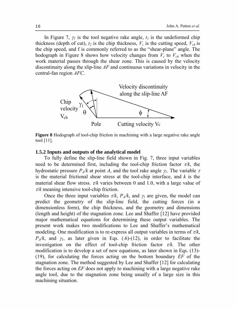
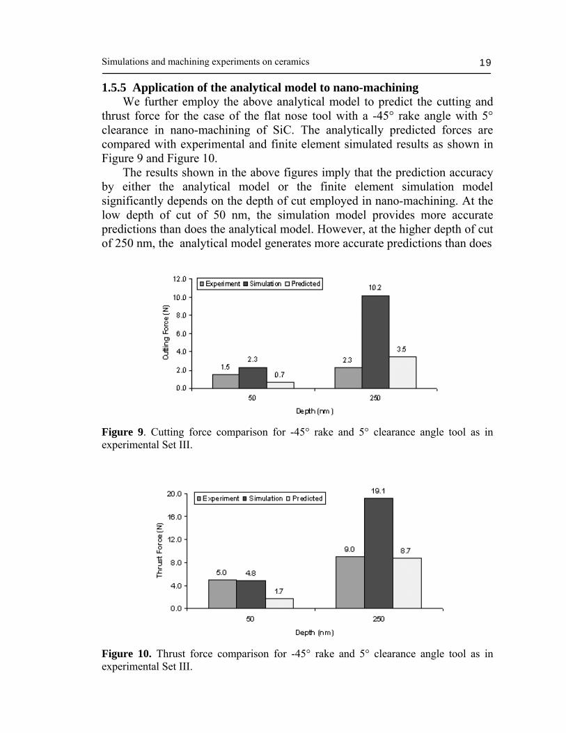
1.5.5 Application of the analytical model to nano-machining We further employ the above analytical model to predict the cutting and thrust force for the case of the flat nose tool with a -45° rake angle with 5° clearance in nano-machining of SiC. The analytically predicted forces are compared with experimental and finite element simulated results as shown in Figure 9 and Figure 10. The results shown in the above figures imply that the prediction accuracy by either the analytical model or the finite element simulation model significantly depends on the depth of cut employed in nano-machining. At the low depth of cut of 50 nm, the simulation model provides more accurate predictions than does the analytical model. However, at the higher depth of cut of 250 nm, the analytical model generates more accurate predictions than does
Figure 9. Cutting force comparison for -45° rake and 5° clearance angle tool as in experimental Set III.
Figure 10. Thrust force comparison for -45° rake and 5° clearance angle tool as in experimental Set III.

John A. Patten et al. 20
the simulation model. Ongoing efforts are made to refine both the analytical model and the finite element simulation model, especially the tool-chip friction and the SiC material constitutive relationship, to minimize the discrepancies between the models and the experiments. 2. Determination of the critical depth of cut in 6-H silicon carbide through fly-cutting 2.1 Background Diamond turning experiments performed on the edge of a single crystal wafer of SiC (6-H) have demonstrated the ability to remove this material in a ductile fashion with the formation of chips similar to conventional metal machining [7]. Further, Patten et al. [7] identified changes in the ductile to brittle transition depth that mapped in an expected way to the six fold symmetry of the crystal structure. Recent work made use of a fly-cutting operation to identify the critical chip thickness along different directions on the (001) cubic face of single crystal silicon [2]. Unlike traditional SPDT, which performs multiple overlapping tool passes on the same surface, fly–cutting with sufficient feed per revolution of the spinning tool permits non-overlapping cuts, i.e. distinct cuts that produce scratch like features. Thus the resulting surface topography of each individual cut provides accurate information about the ductile to brittle transition. However, the chip cross-section for these non-overlapping cuts is considerably different than the overlapping cuts, and therefore analysis and comparison is somewhat complicated by the resultant geometry. 2.2 Experimental setup The fly-cutting experiment involved the use of a hydrostatic diamond turning lathe (Moore Nanotechnology Systems 150AG) consisting of two air bearing spindles – a horizontal fly-cutter spindle (Professional Instruments AC Foot/Flange) and a vertical work spindle (Professional Instruments Twin-Mount). The axes of the two spindles are at right angles to each other and offset by several millimeters. The machine has a programmable linear resolution of 10 nm in the cutting and thrust directions for the fly-cutter spindle, and a rotational resolution of 1.6 arc-seconds on the work spindle. For reference purposes, the silicon fly-cutting setup from [2] is shown in Figure 11. A 2 in. wafer of 6-H single crystal SiC from SiCrystal AG was used as the workpiece for these experiments. The workpiece was glued to an aluminum workpiece chuck that was diamond turned in place to obtain the best possible alignment. The chuck was mounted on a three axis dynamometer (Kistler MiniDyn 9256A2) which was in turn mounted on the vertical work spindle. The dynamometer is used to capture the forces with a usable bandwidth of 1

Simulations and machining experiments on ceramics 21
kHz during the experiment (located below the workpiece). A balanced, aluminum fly-cutter head and diamond tool are mounted onto the fly-cutter spindle, while a capacitance probe (Lion Precision DMT-10 C1-C) placed behind the fly-cutter head triggers the data acquisition for force measurement. Since the tool-workpiece contact occurs only for a small period during a given revolution (less than 1% of a revolution) of the fly-cutter spindle, triggering the data acquisition just before each intermittent cut reduces the data file to a manageable size, even at very high sample rates. Figure 12 provides a schematic of the fly-cutting operation.
Figure 11. Experimental setup similar to that used for fly-cutting of SiC [2].
Figure 12. Schematic of fly-cutting operation [2]. The radius of the fly-cutter is 110mm.

John A. Patten et al. 22
The tool used for the machining experiment is a round nose monocrystalline diamond tool (Chardon Tool #3661) with a -45° rake angle (planar rake), 5° clearance angle and a 1 mm nose radius. The cutting edge radius of the tool is estimated to be 50 nm. A schematic of the tool is provided in Figure 13.
Figure 13. Schematic of diamond tip that is brazed on the tool shank. 2.3 Experimental procedure The experiment was conducted without the use of coolant. Although the workpiece chuck was flat to better than 100 nm, the adhesive used to fix the workpiece to the chuck was uneven and created an out of flatness condition. As a result, a number of preliminary passes were made on the SiC surface to ensure engagement of the workpiece. It is difficult for a human operator to detect tool-workpiece contact given the small depths of cut used in this work (less than 1 µm) so the data acquisition system and force dynamometer was used to determine the tool-workpiece engagement or contact. Once tool-workpiece contact was established, the tool was repositioned over an uncut portion of the workpiece. The cutting test procedure is reasonably sensitive given the difficult to machine characteristics of silicon carbide and are briefly reviewed here. First the workpiece was fed in 250 nm from the previously established touch-off height. In the time it took to start the workpiece spindle rotation, 6 overlapping passes (cuts at the same location collectively shown as cut 1 in Figure 14) had

Simulations and machining experiments on ceramics 23
been made on the workpiece. After this, 3 more distinct (cuts 2, 3 and 4), non-overlapping passes were made on the SiC workpiece. The fly-cutter spindle was maintained at 45 RPM while the work spindle was maintained at 0.625 RPM. Thus, four distinct cuts were made with the diamond tool on the SiC workpiece, on the Si face, at a speed of 82.5 mm/sec.
Figure 14. Cutting and thrust force data from the experiment. 1.2.4 Results from flycutting of SiC The cutting force and thrust force data for the entire duration of the experiment is plotted as shown in Figure 14. The first half of the data set (up to about 8000 counts at 20 kHz) involves no contact between the tool and workpiece. The subsequent rise in the cutting and thrust force values indicate the tool-workpiece contact. After 6 overlapping passes (shown as cut 1 in Figure 14), there is an increase in the force value for cut 2, and then a gradual drop in the values for cut 3 and cut 4. The noise in the force trace is influenced by both the cutting and other environmental effects. During cutting, every effort was made to minimize the external influences but movement of some instrumentation caused sufficient vibration to make a noticeable effect during the latter part of the experiment. Cutting forces from cut 4 are within the noise from the measurement. An average force ratio (apparent coefficient of friction) was calculated for each cut and worked out to be 0.22. A Wyko RST white light interferometer was used to collect the depth profile of each cut. Figure 15 shows one such image of cut 3 with varying depth.

John A. Patten et al. 24
Figure 15. Wyko image of cut 3. Arrow shows direction of cut. 2.5 Discussion of results Cut 1 is the result of 6 overlapping passes. The force data from these passes show an increase in force for the second pass as compared to the first pass. This is because the depth of cut was being increased to achieve a desired maximum depth of cut. After the second pass of cut 1, the depth was not increased any further and as a result the forces decreased with every subsequent pass, as presumably less material (and thus lower forces) was being removed in successive cuts over the same area. While the depth of cut was not increased after the second pass, the tool still made contact with the workpiece, partly as a result of elastic spring back with the tool probably cutting slightly deeper and wider with each subsequent pass. The second (2), third (3) and fourth (4) cuts were made after starting the rotation of the workpiece spindle, i.e. they did not involve overlapping passes. The cutting force data from these cuts however, show a progressive decrease in magnitude. This is attributed to the decrease in depth (contact area) due to tilt in the workpiece setup as explained earlier. Consequently, this led to three decreasing depths for cuts 2, 3, and 4, even though the programmed depth of cut was not changed. For analysis of the depth profile obtained using the Wyko RST, plots are made of a slice (plane) down the center of the cut along its length. The corresponding forces generated as a result of the cuts are plotted along with the depth profiles (as shown in Figure 16 to Figure 19). The forces are used to determine the ductile and brittle regions within the cut. The force data is shown without filtering.

Simulations and machining experiments on ceramics 25
Figure 16. Forces generated from pass 2 of cut 1 while depth profile (lower image) is from final or resultant surface after all six passes of cut 1.
Figure 17. Forces corresponding to cut 2.
Figure 18. Forces corresponding to cut 3.

John A. Patten et al. 26
Figure 19. Thrust force corresponding to cut 4. Cutting force component is indistinguishable from the noise. The cutting forces increase as the tool reaches its maximum depth as shown in Figure 17, Figure 18, and Figure 19. The cutting force from cut 4 is lost in the noise (refer to Figure 14) and is not shown in Figure 19. Since a -45° rake angle tool was used, the thrust forces are larger than the cutting forces as expected. Figure 16 (cut 1 - note this surface profile resulted from six cuts at the same location) shows a catastrophic brittle fracture at depths larger than approximately 600 nm, while Figure 17 (cut 2) and Figure 18 (cut 3), show catastrophic brittle fracture all along the length of the cut. Fracture in the workpiece material, with the material coming out of the surface, indicates fracture occurring behind or in the wake (in the trailing tensile stress field) of the tool [6]. If material came out of the surface in brittle mode in front of the tool, it would be removed subsequently by the tool and would not remain on top of the surface. The resultant depth profile of cut 1 may be due to multiple (overlapped) passes of the tool on the same cut area, i.e. previously generated brittle fracture may be removed in subsequent passes. Figure 20 gives an optical image of cut 1 collected using the Nikon optical microscope. It can be noted that the image was combined from two separate images. The ends of the cut clearly show ductile surfaces as opposed to the center of the cut which shows brittle fracture. Looking at cut 4 in Figure 19, the profile of the cut varies smoothly up to a depth of approximately 70 nm, after which there is an abrupt change in the depth profile indicative of brittle fracture of the material. Again, the material coming up out of the surface is indicative of fracture taking place in the wake of the tool. The profile resumes to a smooth transition as the depth of cut drops back to 70 nm and below, as the tool leaves the workpiece.

Simulations and machining experiments on ceramics 27
Figure 20. Optical image of cut 1 showing ductile regions at either ends of the cut. 3. 3-D scratching (grooving) simulations of silicon and silicon carbide 3.1 Background Scratching with a diamond stylus or cutting tool provides a method of determining the ductile-to-brittle transition (DBT) depth in nominally brittle materials, such as semiconductors and ceramics. The recently developed 3-D grooving module in AdvantEdge provides an alternative means of studying the mechanics of the plastic deformation and material removal during scratching. The grooving/scratching experiments can also be used to simulate a single point cutting edge or grit, such as a grinding grit or polishing particle. In this paper, scratching simulations of Si based on experimental values from Dong [17], and SiC using experimental results from Bhattacharya [18] are presented. 3.2 Silicon simulation 3.2.1 Simulation setup for Si The simulation involves scratching a Si workpiece using a diamond conical tool tip. The tool moves through the workpiece material at a constant penetration depth. The tool is a custom tool, generated using a CAD software program in the STL file format. As per the experiment, the diamond tool is provided with a 5µm tip radius. The tool was initially designed to allow scratching at a depth of 100 nm. To help minimize the number of elements in the mesh, a maximum allowable depth of 300 nm was specified. Beyond this depth (300 nm), the cylindrical surfaces of the tool will interfere or make contact with the workpiece material and affect the simulation in an undesirable or unrealistic manner. The tool used in the simulation is shown in Figure 21.

John A. Patten et al. 28
Figure 21. Tool model used for simulation.
Experimental data for a depth of 71 nm at a speed of 0.305 mm/s indicated ductile material deformation [17]. Initial attempts at using the grooving module were restricted by the simulation software (AdvantEdge) to a minimum depth of approximately 100 nm, and so a programmed depth of 125 nm was used (even though this is larger than the experimental data available). The actual depth achieved after elastic spring back, due to the hardness of the material, was 115 nm, which is still larger than the experimental value of 71 nm used for comparison. The process setup parameters are summarized in Table 8. Table 8. Process parameter listing for simulation of Si simulation. (programmed depth 125 nm).
Parameters Value Unit Geometry
Programmed Depth (feed) 125 nm
(Actual) Depth of Cut, doc 115 nm
Length of Cut, loc 10.0 µm
Cutting Speed, v 0.305 mm/s
Friction factor, µ 0.1 -
For complete details of this work, the interested reader is referred to reference [19]. A typical simulation would progress as shown in Figure 22. The tool obscures the pressures at the tool-workpiece interface and usually the tool is removed from the window, as shown in Figure 23, when presenting the results. This provides a clear view of the pressures, which gives an idea of the interactions taking place at the tool-workpiece interface, i.e. the potential for a HPPT and a ductile material response.

Simulations and machining experiments on ceramics 29
Figure 22. 3-D scratching simulation showing mesh refinement. 3.2.2 Results from simulation of Si An initial estimate of the success of the simulation is obtained by determining the pressures generated at the tool-workpiece contact area. Under steady state conditions, this value is expected to be greater than, or equal to, the hardness of the material for ductile material response of brittle materials [7]. Figure 23 shows a view of the pressure contours generated at the tool-workpiece interface in the simulation, shown with the tool removed. The pressures at the point of contact are equal to or higher than 12 GPa, which is the generally accepted hardness of the single crystal Si material [17].
Figure 23. Pressure plot of workpiece showing values greater than 12 GPa.
John A. Patten et al. 30
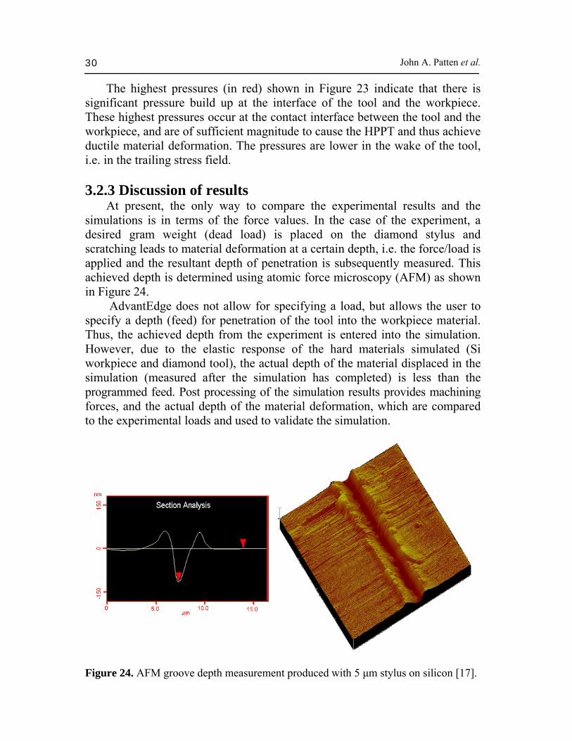
The highest pressures (in red) shown in Figure 23 indicate that there is significant pressure build up at the interface of the tool and the workpiece. These highest pressures occur at the contact interface between the tool and the workpiece, and are of sufficient magnitude to cause the HPPT and thus achieve ductile material deformation. The pressures are lower in the wake of the tool, i.e. in the trailing stress field. 3.2.3 Discussion of results At present, the only way to compare the experimental results and the simulations is in terms of the force values. In the case of the experiment, a desired gram weight (dead load) is placed on the diamond stylus and scratching leads to material deformation at a certain depth, i.e. the force/load is applied and the resultant depth of penetration is subsequently measured. This achieved depth is determined using atomic force microscopy (AFM) as shown in Figure 24. AdvantEdge does not allow for specifying a load, but allows the user to specify a depth (feed) for penetration of the tool into the workpiece material. Thus, the achieved depth from the experiment is entered into the simulation. However, due to the elastic response of the hard materials simulated (Si workpiece and diamond tool), the actual depth of the material displaced in the simulation (measured after the simulation has completed) is less than the programmed feed. Post processing of the simulation results provides machining forces, and the actual depth of the material deformation, which are compared to the experimental loads and used to validate the simulation.
Figure 24. AFM groove depth measurement produced with 5 µm stylus on silicon [17].

Simulations and machining experiments on ceramics 31
The Si scratching experiment [17] did not measure cutting forces (transverse or horizontal force component) and as such only the thrust force (normal loading) is available. This value is compared with the thrust forces achieved from the simulation. The result of the comparison is shown in Figure 25. In the case of Si, the thrust force from the simulation result is comparable, but slightly smaller, than the experimental result, although the simulated depth is larger (115 nm) than the experiment (75 nm). This difference may be due to the material model used for the simulation and/or due to the limitations in the numerical analysis at the nanometer range for 3-D scratching (grooving). But, for a first attempt at using the 3-D grooving module to simulate scratching at the nanoscale in a nominally brittle material, the results are encouraging.
Figure 25. Thrust force values comparison from simulation and experiment. 3.3. Simulation of CVD SiC 3.3.1. Simulation setup for CVD coated SiC The tool used for simulating the scratching of CVD (chemical vapor deposition) coated SiC is the same 5 µm tip diamond tool used in the Si scratching simulations. The process conditions for the simulations are summarized in Table 9. Three simulations were conducted; one with a friction factor (µ) of 0.1, a second with a value of 0.6, and lastly an intermediate value of 0.26. The value of 0.1 was based on the apparent coefficient of friction (Fc/Ft) results obtained from plunge cutting experiments conducted on polycrystalline SiC [18], and as such does not correlate directly to an actual friction factor. The value of 0.6 was used as an upper bound. The apparent COF of 0.26 was also determined

John A. Patten et al. 32
from experiments, where the thrust force was 50 mN and the cutting force was 13 mN [18]. The slow cutting speed of 0.305 mm/s was chosen to match previous experiments on Si [17], and matched the experimental conditions used for scratching SiC [18].
Table 9. Process parameter listing for CVD coated SiC. (programmed depth 125 nm).
Parameters Value Unit Geometry
Programmed Depth (feed) 125 nm
Actual depth, doc 103 nm
Length of Cut, loc 10.0 µm
Cutting Speed, v 0.305 mm/s
Friction factor, µ 0.1, 0.26, 0.6 -
3.3.2 Results from simulation of CVD SiC A quick estimate of the usefulness of the simulation is obtained by determining the pressures at the tool-workpiece interface compared to the material’s hardness (relative to a possible HPPT or stress induced amorphization). For this SiC material, the hardness value is given to be 26 GPa. The plot generated from the simulation with the COF of 0.1 indicates pressures greater than this hardness value, as shown in Figure 26 (with the tool removed). The zone comprising the severe material plastic deformation (red contours) corresponds to areas where the tool-workpiece contact pressures are comparable to the material’s hardness (26 GPa) as shown in Figure 26. A similar plot was obtained for the simulation with COF of 0.6 and 0.26. In the case of the scratching experiments involving CVD SiC both thrust forces and cutting forces are available, along with the achieved depth for material deformation [18]. The results of the comparison of the experimental values with the simulated forces are given in Figure 27. The simulated thrust forces show a gradual drop as the value of µ is increased and all values are in reasonably good agreement with the experimental value. The cutting forces show a gradual increase with increasing µ, as expected. In all cases, the simulated “cutting” forces are lower than the actual measured forces. However, the trend in the data is consistent for the simulations and experimental values, in that lower thrust forces correspond to higher cutting forces for all the data. Further research and experimentation is needed to resolve these apparent discrepancies.

Simulations and machining experiments on ceramics 33
Figure 26. Pressure contour for scratching simulation of SiC with µ of 0.1.
Figure 27. Cutting and thrust force comparison for an approximate depth of 100 nm. 1.3.3.3 Discussion of results from SiC scratching For scratching simulations of CVD SiC, the thrust forces decrease with an increase in COF. The thrust force from the frictional case of µ=0.26 (which matches the experimental force ratio, i.e. the apparent coefficient of friction) shows good agreement with the experimental value, but not in the case of the cutting force, i.e. the experimental cutting (frictional) force is higher than the simulation cutting force. The latter condition is partially due to the fact that the achieved simulation depth is approximately 105 nm, while the experimental

John A. Patten et al. 34
results are closer to 120 nm, which would yield a higher cutting force as found. If the simulation had achieved a larger actual depth, or if experimental data was available for a smaller depth, the comparison between the simulation and experimental cutting forces would be improved, but still different. As both the simulation and experimental depths were ductile, the force should be higher in the case of the 120 nm experimental cut, compared to a depth of 105 nm from the simulation, which is consistent with the results. 4. Conclusions A set of carefully designed numerical simulations were conducted using the software AdvantEdge, both in 2-D and in 3-D, and the machining forces from these simulations were compared with experimental results. The simulations were used to predict the behavior of Si and SiC under a variety of cutting conditions, using the Drucker-Prager yield criterion. The results show that the simulations can predict, with reasonable accuracy, the cutting and thrust forces generated under ductile cutting conditions. However, the simulations were not able to predict, as expected, the forces where the cutting parameters led to brittle machining conditions, because the software (AdvantEdge, [8]) currently only models ductile or plastic deformation and does not include a fracture criterion or brittle material removal mechanisms. The newly developed scratching (grooving) module was used to perform 3-D simulations and the forces and stresses generated by the software at the tool-workpiece interface indicate that pressures are comparable to the material’s hardness, for both Si and SiC, which would provide for a HPPT and a ductile material response. As a first attempt at simulating a 3-D scratching and plastic deformation of nominally hard and brittle materials (Si and SiC) at the nanoscale, the comparison with limited experimental data is quite encouraging and shows promise. Much work presented in this chapter is based on our recent study [19] and interested readers are encouraged to reference [19] for more details. Ongoing efforts are made to investigate the difference in the magnitudes of the cutting force data (comparing the cutting experiments and numerical simulations). Improvements and modifications to the software (AdvantEdge) and material model are being implemented to improve the correlation between the force results between the experiments and simulations. Acknowledgements The author (Patten) would like to thank Dr Wei Gao at Tohoku University for assistance in the SPDT related work and NSF for the High Pressure Phase Transformation of Semiconductors and Ceramics focused research grant (FRG), DMR # 0403650.
Simulations and machining experiments on ceramics 35
References 1. Zolper, J.C. and Skowronski, M. 2005, “Advances in Silicon Carbide Electronics,” MRS Bulletin, 30 (4), pp. 273-278. 2. O’Connor, B.P., Marsh, E.R. and Couey, J.A. 2005, “On the effect of
crystallographic orientation on ductile material removal in Silicon,” Precision Engineering, 29(1), pp. 124-132.
3. Blake, P.N. and Scattergood, R.O. 1990, “Ductile-Regime Machining of Germanium and Silicon”, Journal of American Ceramic Society, v73, n4, pp. 949-957.
4. Arefin, S., Li, X.P., Rahman, M. and He, T. 2005, “Machined Surface and Subsurface in Relation to Cutting Edge Radius in Nanoscale Ductile Cutting of Silicon,” Transactions of NAMRI/SME, 33, pp. 113-119.
5. Ajjarapu S.K., Patten, J.A., Cherukuri, H. and Brand, C.J. 2004, “Numerical Simulations of ductile regime machining of Silicon Nitride using the Drucker-Prager material model”, Proc. Instn Mech. Engrs., 218 (C), pp. 1-6.
6. Patten, J.A., Cherukuri, H., Yan, J. 2005 “Ductile Regime Machining of semiconductors and ceramics”, In: Gogotsi Y, Domnich V, editors, High Pressure Surface Science and Engineering, IoP (Institute of Physics), pp 543-632.
7. Patten, J.A., Gao, W. and Yasuto, K. 2005, “Ductile regime nanomachining of single crystal Silicon Carbide”, ASME Journal of Manufacturing Science and Engineering, 127(8), pp. 522-532.
8. Marusich, T.D. and Askari, E. 2001, Modeling Residual Stress and Workpiece Quality in Machined Surfaces, www.thirdwavesys.com.
9. Kumbera, T.G., Cherukuri H.P., Patten J.A., Brand C.J., Marusich, T.D. 2001, "Numerical Simulations of Ductile Machining of Silcon Nitride", Proceedings of 16th ASPE Annual Meeting, Washington D.C, USA.
10. Noreyan, A.A., 2005, “Molecular dynamics simulations of nanoindentation and nanoscratching of silicon carbide”, Dissertation, University of Toledo.
11. Fang, N. 2005, “Tool-chip friction in machining with a large negative rake angle tool”, Wear, 258(5-6), pp. 890-897.
12. Lee, E.H. and Shaffer, B.W. 1951, “The theory of plasticity applied to a problem of machining”, ASME Transactions, Journal of Applied Mechanics, Vol. 18, pp. 405-413.
13. Ohbuchi, Y. and Obikawa, T. 2003, “Finite element modeling of chip formation in the domain of negative rake angle cutting”, ASME Transactions, Journal of Engineering and Materials Technology, Vol. 125, pp. 324-332.
14. Tanaka H., Sano M. and Shimado S. 2004, Key Engineering Materials, 257-258. 15. Szulfarska I., Kalia R.K., Nakano A., Vashishta, P. 2005, “Atomistic processes
during nanoindentation of amorphous silicon carbide”, App. Phys. Lett., 86, 021915:1-3.
16. Dominich V., Ge D. and Gogotsi Y. 2004, “Indentation-induced phase transformations in semiconductors”, High Pressure Surface Science and Engineering, Gogotsi Y., Domnich V., Eds. IoP (Institute of Physics), pp. 381-442.
17. Dong L. 2006, “In-situ detection and heating of the high pressure metallic phase of silicon during scratching”, PhD Dissertation, University of North Carolina at Charlotte.

John A. Patten et al. 36
18. Bhattacharya, B. 2005, “Ductile regime nano-machining of silicon carbide”, Master’s Thesis, Western Michigan University.
19. Jacob, J. (2006), “Numerical simulations on machining of silicon carbide”, Master’s Thesis, Western Michigan University.


![Concurrent atomistic-continuum simulations of uniaxial ...€¦ · atomic trajectory inside the materials in experiments, numerical simulations via atomistic methods [11,12] and discrete](https://img.dokumen.tips/doc/110x75/5fb2485e21a30672d07b36b4/concurrent-atomistic-continuum-simulations-of-uniaxial-atomic-trajectory-inside.jpg)