Embed Size (px)
Citation preview

1
Novel Materials for Silicon Based Photonics
by
Qingyang Du
B.S., Materials Physics
University of Science and Technology of China, 2012
SUBMITTED TO THE DEPARTMENT OF MATERIALS SCIENCE AND
ENGINEERING IN PARTIAL FULFILLMENT OF THE REQUIREMENTS FOR THE
DEGREE OF
DOCTOR OF PHILOSOPHY
AT THE
MASSACHUSETTS INSTITUTE OF TECHNOLOGY
September 2018
© 2018 Massachusetts Institute of Technology. All Rights Reserved.
Signature of Author: ____________________________________________________________
Department of Materials Science and Engineering
August 8th, 2018
Certified by: ___________________________________________________________________
Juejun Hu
Merton C. Flemings Career Development
Associate Professor of Materials Science and Engineering
Thesis Supervisor
Accepted by: ____________________________________________________________
Donald Sadoway
John F. Elliott Professor of Materials Chemistry
Chair, Departmental Committee on Graduate Student

2

3
To my grandfather 杜绍明
谨以此论文献给我的祖父,愿您在另一个世界永远快乐

4
5
Novel Materials for Silicon Based
Photonics
by
Qingyang Du
Submitted to the Department of Materials Science and Engineering on August 8th, in Partial
Fulfillment of the Requirement for the Degree of Doctor of Philosophy in Materials Science and
Engineering
Abstract
A complete photonic chip must include the following components: a light source, usually
lasers, an isolator, a waveguide, a modulator and a photodetector. Limited by material
intrinsic properties, silicon alone cannot realize all the above mentioned functions. The
development of silicon photonics has found its way through exploiting novel materials as
hybrid platforms to manufacture various devices and systems.
In this thesis, we focus on the development of novel material in emerging needs of
broadband coherent light source and optical isolators. Chalcogenide glass stands out among
the candidates for light generation and sensing due to its large non-linear figure of merit
and wide transparency window in the IR spectral range, while magnetic garnet still presents
the best device performance among magneto-optical isolators owing to the ease of phase
formation and relatively low material absorption.

6
We first investigated the fabrication technology of chalcogenide glass and developed a
process flow to produce low loss planar chalcogenide glass waveguides. Using electron
beam lithography to minimize sidewall roughness and reactive ion etch to achieve vertical
sidewalls. We managed to demonstrate a record low loss of 0.5 dB/cm in single mode core
chalcogenide waveguides. Based on this low loss platform, we integrated a supercontinuum
light source onto a sensor chip. Our work presented a step forward towards miniaturization
photonic sensor chips.
Next, we focused on a hybrid platform of chalcogenide glass and magnetic garnet. By
carefully designing device architecture, a monolithically integrated TM polarized magneto-
optical (MO) isolator with 3 dB insertion loss and 40 dB isolation ratio was demonstrated.
Both parameter sets record among current monolithically integrated on-chip MO isolators.
Meanwhile, we also demonstrated a monolithically integrated MO isolator with TE
polarization featuring 11.5 dB insertion loss and 20 dB isolation ratio.
Lastly, we leveraged cavity enhanced spectroscopy platform to study radiation induced
effect on SiNx, a-Si and SiC materials. We found a refractive index modulation to the order
of 10-3 after receiving 10 Mrad Gamma radiation dose.
Thesis supervisor: Juejun Hu
Title: Merton C. Flemings Career Development Associate Professor of Materials Science and
Engineering

7
Table of Content
Abstract ...............................................................................................................................5
Acknowledgement ............................................................................................................12
Chapter 1. Introduction ..................................................................................................17
1.1 Limitations and Challenges in Silicon Photonics ................................................................ 17
1.2 Chalcogenide glass material ................................................................................................. 18
1.3 Magnetic garnet oxide material ............................................................................................ 20
1.4 Thesis outline ........................................................................................................................ 21
Reference .................................................................................................................................... 23
Chapter 2. Low Loss Chalcogenide Glass Photonics ...................................................24
2.1 Chalcogenide Glass as Waveguide ...................................................................................... 24
2.2 Current Fabrication Technologies of Chalcogenide Glass Photonics ................................. 25
2.3 Fabrication Process Optimization ........................................................................................ 26
2.4 Loss Analysis ....................................................................................................................... 32
2.5 Conclusion ............................................................................................................................ 36
Reference .................................................................................................................................... 37
Chapter 3. On-Chip Supercontinuum Integrated Chalcogenide Chemical Sensor ..38
3.1 Limitation of Current Photonic Sensor Chips ..................................................................... 38
3.2 On-Chip Supercontinuum Generation in Chalcogenide Glass ............................................ 39
3.3 Demonstration of Chloroform Sensing ................................................................................ 46
3.4 Conclusion ............................................................................................................................ 48

8
Reference .................................................................................................................................... 49
Chapter 4. Monolithically Integration of On-chip Magneto-optical Isolators ..........51
4.1 Magneto-optical (MO) Effect .............................................................................................. 51
4.2 Introduction to isolator ........................................................................................................ 53
4.3 Magnetic Garnet .................................................................................................................. 58
4.4 Novel Design of next generation TM isolator ..................................................................... 62
4.5 Demonstration of next generation TM isolator ................................................................... 67
4.6 TE MO isolators .................................................................................................................. 79
4.7 Discussion and outlook ........................................................................................................ 82
4.8 Conclusion ............................................................................................................................ 86
Reference .................................................................................................................................... 87
Chapter 5. Radiation Induced Effects in Silicon Photonic Materials and Devices ...90
5.1 Radiation Overview ............................................................................................................. 90
5.2 Stopping Range of Ions in Mater (SRIM) ............................................................................ 91
5.3 Gamma Radiation Damage in a-Si and SiNx Materials and Devices .................................. 96
5.4 Gamma Radiation Damage in a-SiC Materials and Devices ............................................. 105
5.5 Conclusion .......................................................................................................................... 108
Reference .................................................................................................................................. 109
Chapter 6. Conclusion and Future Work ...................................................................111
5.1 Radiation Overview ........................................................................................................... 111
5.2 Stopping Range of Ions in Mater (SRIM) .......................................................................... 112

9
List of Figures
Figure 1-1 A Comparison of transparency window of silica, silicon,
chalcogenides, heavy-metal oxides and halides is shown on the
bottom. The window is matched to the scale of optical spectrum
shown above. On top of the figure, typical functional groups
absorption region are displayed. We can see that chalcogenide glass
covers most of their spectral range.
12
Figure 1-2 Crystal structure of yttrium ion garnet. The pink and blue region
marked tetrahedral site and octahedral site, respectively. 14
Figure 2-1 SEM images of: a, b) chlorine-etched GSS waveguides with silicon
oxide passivation coating; the grainy surface texture comes from
gold coating applied to reduce electrostatic charging during SEM
imaging; c) chlorine-etched GSS waveguide without silicon oxide
passivation coating; d, e) fluorine-etched GSS waveguides.
23
Figure 2-2 a) Schematic diagram showing the XPS tilted beam analysis
configuration. The grating has a 400 nm line width with 800 nm
period. b) XPS spectrum showing the presence of Si and O, and trace
amounts of C, F in the coating layer.
24
Figure 2-3 Optical microscope images of fabricated a) micro-disk and b) micro-
ring resonators. c-d) Transmission spectra of c) micro-ring
resonator; and d) micro-disk resonator etched using the fluorine
chemistry. The red curves are Lorentzian fit of the spectra
27
Figure 2-4 Waveguide sidewall roughness analysis example: a) SEM top-view
image of a fluorine etched waveguide; the grainy surface texture
comes from gold coating applied to reduce electrostatic charging
during SEM imaging. b) Waveguide edge extracted from the SEM
image. c) PSD function of sidewall roughness (black line). The red
line represents exponential model fit.
28
Figure 3-1 (a) Refractive index dispersion of the Ge22Sb18Se60 glass film
measured using ellipsometry; inset schematically depicts the
waveguide structure; (b) Simulated GVD of GeSbSe waveguides with
varying widths (W) and a fixed core thickness H = 400 nm.
34
Figure 3-2 (a) Top-view optical micrograph of the zigzag GeSbSe waveguides;
(b) SEM cross-sectional image of a 0.95 µm (W) × 0.4 µm (H)
GeSbSe waveguide; (c) The experimental setup of on-chip SC
generation and sensing; (d) Block diagram of home-built
femtosecond laser module (OC: Optical coupler, WDM: wavelength
division multiplexer, SA: graphene saturable absorber, PC:
polarization controller)
36

10
Figure 3-3 SC spectra in GeSbSe waveguides: (a) SC spectra from waveguides
with different widths W; when W = 0.95 µm, the zero-dispersion
point of the waveguide coincides with the pump wavelength; (b) SC
generation of GeSbSe waveguides with the optimal geometry (W =
0.95 µm, H = 0.4 µm) and varying lengths; (c) SC spectra from a 21-
mm-long GeSbSe waveguide (W = 0.95 µm, H = 0.4 µm) at different
pump power levels. The power quoted here represent the average
optical power coupled into the waveguide.
38
Figure 3-4 (a) SC spectra measured on GeSbSe waveguides of different lengths
L when immersed in chloroform; the triangle marks the optical
absorption at 1695 nm calibrated using a benchtop UV-Vis
spectrometer for an equivalent waveguide path length L = 21 mm;
(b) SC spectra taken on a 21-mm-long GeSbSe waveguide immersed
in CHCl3-CCl4 solutions of varying volume concentration ratios; (c)
measured peak absorption at 1695 nm versus the GeSbSe waveguide
length used in the experiment: the linear relation indicates that the
classical Lambert’s law is obeyed; inset shows the mode profile
simulated by finite difference method.
40
Figure 4-1 (a) Schematic of a nonreciprocal optical resonator structure and
cross-section (inset) through the garnet-clad section of the Si
waveguide. (b) Schematic showing a Faraday rotation waveguide
isolator and cross-section (inset) of the garnet-clad waveguide. (c)
Cross-sectional image of a fabricated one-dimensional magneto-
photonic crystal consisting of magneto-optical garnet (Ce:YIG,
cerium-doped yttrium iron garnet) between two Bragg mirrors. (d)
Schematic and cross-section (inset) of a Mach–Zehnder transverse
electric (TE) mode isolator with Ce:YIG mesas adjacent to the
sidewalls of the waveguide. Note: a-Si:H, hydrogenated amorphous
silicon.
49
Figure 4-2 (a) X-ray diffraction (θ− 2θ scans of pulsed laser deposition cerium-
doped yttrium iron garnet (Ce:YIG) and YIG multilayer garnet films
after rapid thermal annealing at 800°C for 5 min on silicon, showing
characteristic garnet peaks.] (b) Scans of sputtered TbIG (TIG,
terbium iron garnet) on Si and quartz substrates, showing
characteristic garnet peaks. (c) In-plane hysteresis loops and (d) out-
of-plane Faraday rotation hysteresis loops at a wavelength (λ) of
1550 nm, with magnetic field and light propagation perpendicular to
the film, for sputtered Ce:YIG on Si substrates annealed at 800°C for
various times. Inset shows the saturation Faraday rotation
dependence on annealing time.] (e) Bright-field transmission
electron microscope (TEM) cross-sectional image of
YIG/Ce:YIG/silica/Si, showing large grained YIG top seed layer and
fine grained Ce:YIG. Inset shows the high resolution TEM image of
the interface between the film and Si substrate (f) Spectral
dependence of figure of merit (FOM) of single-crystal Ce:YIG films
with different crystal orientation on a garnet substrate, with
magnetic field and light propagation perpendicular to the film.
53

11
Figure 4-3 (a) Schematic transmission spectra of a resonator isolator; (b)
resonator isolator structure demonstrated in [6]; (c) cross-sectional
SEM image of a SOI waveguide covered with deposited magneto-
optical oxides; (d) breakup of loss contributions in the isolator
device in [6].
56
Figure 4-4 (a) Tilted-view and (b) cross-sectional schematic of the new isolator
design; (c) nonreciprocal phase shift and waveguide figure of merit
computed as functions of the strip-loaded waveguide core refractive
index: the insets are modal profiles of strip-loaded waveguides when
the core material is chosen as silicon nitride (n = 2.0), GeSbSe glass
(n = 2.7), and amorphous silicon (n = 3.6), where the scale bars
correspond to 500 nm; (d) fabrication process flow for the isolator
device.
61
Figure 4-5 (a) Top-view optical micrograph of a fabricated resonator isolator;
(b) cross-sectional SEM image of the strip-loaded waveguide
showing the layer structures
65
Figure 4-6 (a) Experimental setup for characterization of the isolator device:
(1) and (2) indicate optical paths used to interrogate the device in
forward and backward propagating directions, respectively; (b)
transmission spectra of the isolator: inset shows the same spectra
over several free spectral ranges of the resonator; (c) resonant peak
wavelengths of the device repeatedly measured for 5 consecutive
times; (d) spectral dispersion of the nonreciprocal resonant
wavelength shift measured in the isolator.
66
Figure 4-7 Transmittance spectrum of a strip loaded GeSbSe racetrack
resonator on a SiO2 substrate with vertical tapers. 72
Figure 4-8 a) optical microscope image (top view) of as-fabricated SiN
racetrack isolator. (b) forward and backward transmission spectrum
of SiN isolator, we observed a 15 pm peak shift. (c) cross-sectional
SEM image at the window region. (d) Recorded transmission peak
position of SiN racetrack isolator. The measurement was conducted
by swithching light propagation direction for 5 times consecutively.
74
Figure 4-9 (a) Quasi-transverse magnetic (TM) mode profile and (b) cross-
sectional structure of a magneto-optical (MO)-film capped silicon-
on-insulator (SOI) waveguide; (c) ratio of waveguide nonreciprocal
phase shift and the Faraday rotation of the MO material in the SOI
waveguide illustrated in (b); the dotted line delineates the waveguide
single-mode (left) and multi-mode (right) regimes. (d) Simulated
insertion losses of isolators versus the MO material figure of merit
(FOM). Three different device configurations: micro-ring, Faraday
rotator, and Mach–Zehnder interferometers (MZI) are compared.
Here, the micro-ring and MZI isolators consist of SOI waveguides
shown in (b) with a core width of 450 nm and a height of 220 nm.
The dotted line corresponds to the best experimentally assessed
FOM in deposited cerium-doped yttrium iron garnet (Ce:YIG) films.
78

12
Figure 5-1 Stopping range plot of alpha particles with different energies. 85
Figure 5-2 LET and NIEL of alpha particle damage with energies ranging from
20KeV to 100KeV on silicon nitride film. From the simulation, we
conclude that for silicon nitride device with 400 nm thickness, alpha
irradiation with energy of ~60 keV should be chosen in our
irradiation experiments as it can induce most damage inside the
material, and can yield insights into the upper and lower limits for
rad-hardness.
86
Figure 5-3 Transmission spectra of silicon nitride resonators before and after
alpha irradiation
88
Figure 5-4 (a) Top-view optical microscope image of an a-Si micro-ring
resonator; (b) transmission spectra of the a-Si resonator before
(black curve) and after (red curve) receiving 2 Mrad gamma
irradiation
90
Figure 5-5 HRTEM images of a-Si sample before (a) and after (b) 20 Mrad
radiation. (c) and (d) are the corresponding images of a SiNx film
before and after radiation under same dose. (e) and (f): XRD spectra
of a-Si and SiNx thin film before and after 20 Mrad gamma
irradiation, respectively.
93
Figure 5-6 (a) and (c): Si 2p peak from a high resolution XPS scan of as-
deposited (a) a-Si and (c) SiNx films. The spectra are deconvoluted
into different Si bonding states, where the red curves correspond to
Si-O bond, the blue curve are assigned to Si-Si bond and the pink
curves are associated with Si-N bond. The Insets show the sums of
the deconvoluted peaks, indicating good fitting quality; (b) and (d)
calculated surface Si-O bond fraction for (b) a-Si and (d) SiNx
samples irradiated in argon (red) and ambient air (black).
95
Figure 5-7 Dependences of refractive index changes on cumulative gamma
radiation dose in (a) a-Si and (b) SiNx inferred from optical
resonator measurements.
96
Figure 5-8 (a) Optical microscope image silicon carbide micro-resonator; (b)
Optical mode of the fabricated silicon carbide waveguide with 1 μm
width; SEM micrographs are shown (c) top view and (d) cross
section, respectively.
99
Figure 5-9 (a) Transmission spectra of silicon carbide resonator before and
after 2 Mrad gamma radiation in air; (b) quantitative analysis of
peak shift with respect to radiation dose; (c) linear extrapolation of
effective index change, the result shows a 0.0015 index change in
silicon carbide material after receiving 2 Mrad. (d) silicon carbide
core refractive index change with radiation dose.
100

13
Acknowledgement
After staring at this blank page for nearly half an hour, I finally starting typing this very
last part of my PhD thesis. Memories of the past four years flashes back and forth in front
of my eyes. Happiness and bitterness, joys and tears. It is the time I spent with those around
me made my life in MIT. I would like to take this special opportunities to express my
gratitude to all of you.
I first would like to express my deepest respect and gratitude to my advisor Prof. Juejun
Hu. During your six years of mentorship, you have always been like a father who would
instruct me and guide me with patience and wisdom. You never give me up when I make
serious mistakes and it is you who always have faith in me correcting my problems. You
have also been like a friend who would share his life stories and give me courage when I
was down. It is your passion that fascinated me into the field of photonics and your wisdom
that illuminated my research directions. Your excellent leadership of the group, addiction
to science and broad visions are the valuable treasure I always admire and learn from.
Thank you JJ.
Next, I would like to thank Dr. Jurgen Michel and Prof. Caroline Ross as my thesis
committee members. Both of your suggestions benefited me on my research works. Dr.
Michel’s smart mind always shed light upon me when I went into a problem I could not
solve. Prof. Ross is so nice to work with. You generously shared me access to all your lab

14
equipment where I learned plenty of skills from. I also like your lecture on magnetic
materials and it filled my knowledge gap of magnetism in materials.
I also would like to thank Prof. Lionel C. Kimerling and Dr. Anuradha Aggarwal. Kim
offered me a TA in 2017 spring, where I gained my first experience with teaching. You
gave me lots of freedom in developing me own teaching skills and give your experiences
on being a good teacher. I worked with Dr. Anu on a research project about radiation
induced damage effect in photonic chips. Anu is nice to work with and discussion with you
has been very helpful in my researches. I feel our fruitful collaboration full of pleasant.
I would like to thank the entire PMAT family. Dr. Tian Gu, Dr. Yi zou, Prof. Hongtao Lin,
Dr. Okechukwu Ogbuu, Dr. Lan Li, Dr. Mikhail Shalaginov, Dr. Haijie Zuo, Dr. Shaoliang
Yu, Dr. Carlos A. Rios Ocampo, Dr. Samuel Serna-Otalvaro. Duanhui Li, Derek Kita,
Jerome Michon, Sarah Geiger, Gufan Yin, Yifei Zhang, Skylar Deckoff-Jones and Bin
Huang. Discussion and doing research with you have always been very helpful. I appreciate
all your kindness and I enjoy all my time with you.
I would like to express my thanks to my close collaborators and friends in academia, Prof.
Lei Bi, Prof. Qinghui Yang, Prof. Li Zhang, Prof. Zhengqian Luo, and Prof. Wei Zhang. I
benefitted a lot both in knowledge and vision from discussion on our researches project. In
addition, you are also my close friends in my life. Your generosity and companionship
make me warm in my heart. I do miss the days we work and dine together.

15
I would like to thank my close friends in MIT. Dr. Zhaohong Han, Dr. Junying Li, Dr.
Yizhong Huang, Huizhang Zhong and Duanhui Li. “A friend in need is a friend indeed”.
You are the ones I can turn into when I’m overwhelmed and depressed. You always are so
considerate and nice to me. The days we did research, had fun and dined together shapes
my best memories in MIT.
I would like to thank my close friends in UD as well. Xuesong Liu, Dr. Jin Sha, Dr.
Zeguang Zou, Chang Liu, Xinhui Jiang, Dr. Changgen Mei, Dr. Xi Lin and Jing Zhang.
You are the ones I first meet when I’m alone in a foreign country for the first time. Your
companionship and friendship are the most valuable treasure to me. You walked me
through the most challenging days in life. Thank you all.
我要在此感谢我的父母,你们从小对我的耐心抚养和教导才让我有了能站在 MIT
舞台上的今天。你们坚忍不拔永不言败的性格与勇往直前的勇气深深影响着我。我
爱你们,祝你们永远健康快乐。
I would like to thank all the board members of Chinese Students and Scholars Association
(CSSA), after joined CSSA in 2014. I really enjoyed each culture event and seminars
hosted by CSSA. The board meeting every two weeks enhanced my communication skill
and strategic decision making. It is CSSA that made my life colorful and benefited me from
detailed event planning skills and leaderships. I owe CSSA family a big thanks.

16
Lastly, I would like to express my special thanks and deep affection to Yaner, my closest
partner in research and my love in life. You are an angel who shines the sunlight into the
darkness and lights up my sky. The time we spent together are the sweetest and the most
cherishing days in my life. Whatever life holds in store for us, hand in hand, faith to faith.
Believe in our love, nothing can stop us.

17
Chapter 1. Introduction
1.1 Limitations and Challenges in Silicon Photonics
Silicon microphotonics, active and passive planar photonic components employed in
monolithic electronic-photonic circuits, is a preferred platform for power efficient, high
performance computing, imaging and sensing systems. This synergistic chip functionality
provides distance independent communication with x103 improvements in energy-delay
product and bandwidth density. Given the wide range of emerging applications, the
development of silicon photonics are still hindered by its limitations: First, silicon material
has limited transmittance at UV-vis and mid-IR or longer spectral range. It greatly stopped
silicon photonics as candidates of applications in waveguiding and sensing in those
wavelengths. In addition, unlike electronics, silicon, as a single crystalline photonic
material, which requires a lower index cladding material to confine light, has intrinsic
epitaxial growth requirement. Current silicon photonics strongly relies on SmartCut
technology to make silicon-on-insulator (SOI) wafers, which is costly and up to ~ $1000
per wafer. Moreover, large two-photon absorption in silicon makes the material lossy when
using high powers and in nonlinear photonics. Therefore, researchers has developed a wide
range of other materials, including silicon nitride, amorphous and polysilicon as well as
glass materials, metal oxides and semiconductors as hybrid platform to fulfill those
application requirements. In this thesis, we focus on chalcogenide glass as waveguide
guiding and garnet oxide as hybrid platform to realize on-chip sensing and on-chip isolation
device chips.

18
1.2 Chalcogenide Glass Material
Chalcogenide glasses are referred to a broad family of inorganic amorphous materials
containing one or more Group IV chalcogen elements, namely sulfur, selenium, and
tellurium. Chalcogenide glasses, like their counterpart oxides, lacks long range order where
atoms are connected via glass networks. This amorphous feature allows chalcogenide glass
easily be integrated onto any substrate via thermal evaporation [1]. In addition, Unlike SiO2
and other oxide glasses, chalcogenide glass comp rise of heavy atoms, such as Se, Sb and
Te. These ions have lower phonon energy which give rise to its well-known wide
transparency window [2]. (Fig. 1-1) Therefore, chalcogenide glass has been widely used
as waveguiding and sensing platform in IR spectral range [3, 4]. Moreover, chalcogenide
glass yields higher Kerr non-linear figure-of-merit (FOM) which is defined as equation 1:
FOM = n2/α2 (1)
where n2 is the non-linear refractive index associated with third order nonlinear
susceptibility (χ3), and α2 is the non-linear loss. According to Miller’s rule [5], the third
order susceptibility is usually to the quadrant of first order susceptibility. Therefore, larger
linear refractive index chalcogenide glass usually has much higher n2 value than those in
oxide glasses. Meanwhile, nonlinear absorption also can happen in chalcogenide glass,
where two photon absorption (TPA) is the dominant loss contributor. In this process, free
carriers in the valence band can absorb multiple photons to reach conduction band.
Compared with semiconductors, low concentration of free carriers in the glass networks
makes the nonlinear absorption small. Based on the discussion above, chalcogenide glasses
exhibited both high Kerr non-linear refractive index and low non-linear absorption (i.e.

19
high non-linear FOM) and hence chalcogenide glass has been a better candidates than
semiconductors in nonlinear optics.
Figure 1-1. A Comparison of transparency window of silica, silicon, chalcogenides, heavy-metal
oxides and halides is shown on the bottom. The window is matched to the scale of optical spectrum
shown above. On top of the figure, typical functional groups absorption region are displayed. We
can see that chalcogenide glass covers most of their spectral range.
20
1.3 Magnetic Garnet Oxide Material
Magnetic garnet are cubic crystals having 8 chemical formula per unit cell. The formula of
garnets are {c3+}3[a3+]2(d
3+)3O12, this means there are three possible sites per unit cell for a
cation with respect to its surrounding oxygen anion. The dodecahedral sites {c} are usually
occupied by large rare earth atoms, like Ce, Y, and Bi, while the octahedral site [a] and
tetrahedral site (b) are occupied by smaller atoms like Fe and Al. The crystal structure of
Y3Fe5O12 (YIG) is shown in Figure 1-2. Due to 180 degree superexhange effect, [a] site
and (b) site are coupled antiferromagnetically, resulting in a ferrimagnetic crystal.
Typically, to enhance magneto-optical effect, YIG is usually doped with Ce and Bi.
Electron transitions in Ce3+ are magnetically coupled to Fe3+ in Ce:YIG [33] while 6s2
electrons of Bi promotes the orbital splitting of Fe3+ in Bi:YIG [32], where both cases
contributed to larger magneto-optical effects. However, monolithic integration of these
materials has been challenging due to large lattice mismatch of YIG (12.376 Å) and Si
(5.43 Å). In addition, coefficient of thermal expansion of YIG (10.4×10⁻⁶/℃) is more than
4 times larger than that of Si (2.33×10⁻⁶/℃). Monolithically integration of polycrystalline
YIG film on Si is possible. Nevertheless, cracks tends to form when YIG thickness exceeds
certain critical value. [36] Therefore, development of monolithic integration technology of
garnet oxide onto Si is the key to make high performance devices.

21
Figure 1-2. Crystal structure of yttrium ion garnet. The pink and blue region marked tetrahedral
site and octahedral site, respectively.
1.4 Thesis Outline
In this thesis, we focused on solving the challenges and limitations by integrating
chalcogenide glass and magnetic garnet oxide into silicon photonics. We introduced two
types of devices: a light source integrated chemical sensor chip and a magneto-optical
isolator.

22
Chapter 1 presented the motivations of exploring novel materials for silicon photonics, and
the fundamentals of the two materials: chalcogenide glass and garnet oxide are introduced.
In chapter 2, we compared current fabrication technology of making chalcogenide glass
photonics and exploited a process utilizing electron-beam-lithography and reactive ion
etching to produce low loss chalcogenide glass waveguides and resonators. Our results
represented the lowest propagation loss in single mode core chalcogenide glass waveguides.
Chapter 3 introduced the work of the first monolithic combination of a supercontinuum
light source and a sensor on to a single chip. We made use of large non-linear FOM and
wide transparency window advantages of chalcogenide glass. Pumped by a femto-second
laser and immersed in chemicals, the chip exhibited excellent broadband coherent light
generation without compromising its sensing capabilities. An ultra-compact sensor system
could be built if we combine this sensor chip with palm-sized fs-laser and on-chip digital
FTIR spectrometer. In Chapter 4, we dedicated to optimize the device performance metrics
using facile designs and improved film deposition technology of magneto-optical isolators.
Combining material design and device engineering, we successfully reduced the insertion
loss to 3 dB and increased the isolation ratio to 40 dB, both values sets the record in current
monolithically integrated TM-polarized magneto-optical isolator. The device architecture
had a strip-loaded chalcogenide glass strip-loaded waveguide and a garnet oxide cladding.
In the meantime, we demonstrated the first monolithically integrated non-reciprocal phase
shift based magneto-optical isolator with TE polarization. This device featured an insertion
loss of 11.5 dB and 20 dB of isolation ratio. Finally, as a growing trend in the development
of silicon photonics, silicon photonic chips are starting to be widely used in radiation-hard
environments for example near nuclear reactor and in space. In chapter 5, we conducted a

23
systematic study of radiation induced effects in SiNx, a-Si and SiC, all of which are
commonly used materials in silicon photonics. We found a modification of refractive index
to the order of 10-3 while no obvious change in extinction coefficient after receiving up to
10 Mrad cumulative gamma radiation dose. We also developed a technology of making
radiation hard devices by engineering the device structure.
Reference
(1) J. Hu, V. Tarasov, N. Carlie, L. Petit, A. Agarwal, K. Richardson, and L. Kimerling, Opt. Mater. 30, 1560 (2008).
(2) J. Hu, N. Carlie, L. Petit, A. Agarwal, K. Richardson, and L. C. Kimerling, J. Lightwave Technol. 27, 5240-5245 (2009)
(3) J. Hu, V. Tarasov, N. Carlie, L. Petit, A. Agarwal, K. Richardson, and L. C. Kimerling, Opt. Express 15, 2307 (2007).
(4) J. Hu, N. Feng, N. Carlie, J. Wang, L. Petit, A. Agarwal, K. Richardson, and L. C. Kimerling, Opt. Express 15, 14566 (2007)
(5) E. Vogel, M. Weber, and D. Krol, Phys. Chem. Glasses 32, 231-254 (1991).
(6) M. Gomi, H. Furuyama and M. Abe, J. J. Appl. Phys., 29, L99 (1991)
(7) G. F. Dionne and G. A. Allen, J. Appl. Phys., 75, 6372 (2004)
(8) T. Boudiar, B. Payet-Gervy, M. -F. Blanc-Mignon, J. -J. Rousseau, M. Le Berre and H. Joisten, J. Magn. Magn. Mater, 284, 77 (2004)

24
CHAPTER 2
Low Loss Chalcogenide Glass Photonics
2.1 Chalcogenide Glass as Waveguide
Chalcogenide glasses are glass materials containing chalcogen atoms (S, Se and Te). They
are widely recognized as the material of choice for all-optical signal processing and sensing
due to its wide transparency window in mid-infrared [1-13]. Their high Kerr non-linearity
and low two photon absorption (i.e. high non-linear figure of merit) gives the advantages
in non-linear light generation and modulation [1, 3]. In addition, the amorphous nature and
room temperature processes allows chalcogenide glass to integrate onto any substrate
without considering epitaxial lattice match and thermal budget. This unique feature makes
chalcogenide glass suitable for flexible integration [4]. In general, their high refractive
index and small mode volume allow chalcogenide glass to suffer less from parasitic
excessive radiative losses compared to silica glasses. In fact, chalcogenide glass has been
widely used as waveguides in Mid-IR optical fibers and in particular, Vanier [13] has
demonstrated a propagation loss as low as 0.002 dB/cm in a chalcogenide microsphere
resonators. However, the technology of fabricating low loss integrated chalcogenide glass
waveguides are still not fully developed as losses are reported to be 0.05 dB/cm for large
core rib waveguide [11] and 0.84 dB/cm for single mode waveguide [12]. This is more than
an order of magnitude higher than that in optical fibers. It is apparent fabrication induced
sidewall roughness are the dominant loss contributors for on-chip chalcogenide glass
waveguide.
25
In this chapter, we compare current existing fabrication technology and proposed an
optimized process for on-chip chalcogenide glasses.
2.2 Current Fabrication Technologies of Chalcogenide Glass Photonics
Planar chalcogenide glass photonic device fabrication using standard semiconductor
microfabrication techniques has been studied extensively. Those techniques include
plasma dry etching[11, 12], wet etching [6], ion milling [7], nanoimprint [8,9] and lift-off
[10]. In wet etching, chips are immersed in liquid solutions to trigger chemical reactions of
chemical etching. The etching is usually isotropic and difficult to control the etching profile.
Creating vertical and smooth sidewalls are extremely challenging and thus not applicable
in mass production lines. In contrast, ion milling, which uses high energy ions, usually Ar+,
to bombard away materials to be etched. Benefitting from high etching ability to various
materials and achieving highly vertical sidewalls, ion milling stands as a better candidate
than wet processes. However, lacking of etching selectivity and low etch rate have strongly
limited ion milling technology to hard material (high Z number elements) etching process
in current fabrication lines. Lift-off processes, where film deposition is performed after
chip patterning, have advantages in producing residue-free waveguides after lift-off. This
technology is still limited in CMOS lines due to relatively low fabrication yield and
tolerance. In nanoimprint technology, a PDMS stamp model is first build and then
thermally pressed onto chalcogenide glass chips while heating near its glass transition
temperature. The waveguide will be formed thermodynamically and yields smooth
sidewalls. Yet, the complex process does not meet large scale fabrication standard. Dry

26
plasma etching technologies, including inductive coupled plasma (ICP) etching and
reactive ion etching (RIE), are the most commonly used process in current fabrication
foundries. These technologies provide near vertical sidewall and high fabrication yield. In
addition, fast etching rate and highly selective etching chemistry enabled precise etching
control. Therefore, we focused on study on plasma dry etching technology
2.3 Fabrication Process Optimization
Our prior work had relied on UV photolithography for ChG microphotonic device
fabrication, although large sidewall roughness (10-15 nm root mean square [15]) due to the
limited feature resolution can compromise the resulting device performance. In this paper,
we report a systematic study of low-loss ChG device processing using electron beam
lithography coupled with reactive ion dry etching. Compared to UV photolithography,
electron beam (e-beam) lithography is known to offer deep-sub-micron resolution and
significantly reduced pattern edge roughness, and is therefore suited for low-loss, high-
index-contrast ChG device processing. Both chlorine and fluorine etching gases are
investigated, as both chemistries have been adopted for low-loss ChG device patterning
[11, 12].
The ChG devices were fabricated on 6" silicon wafers with 3 µm thermally grown oxide
coating (Silicon Quest International). A piranha clean was performed prior to film
deposition to remove any organic residue from the wafer surface. Subsequently, Ge23Sb7S70
(GSS) bulk glass prepared by conventional melt/quench protocols previously reported [16]

27
was thermally evaporated onto the wafer to form a 450-nm-thick ChG film using
established protocols [16]. We chose the GSS composition over the classical As2S3 or
As2Se3 systems given the superior oxidation-resistance of GSS glass, whereas As2S3 or
As2Se3 glasses are prone to surface oxidation [9]. The deposition rate was maintained at 15
Å/s. A 400-nm-thick ZEP-520A resist (ZEON Chemicals) layer was then spun onto the
glass film and exposed by an Elionix ELS-F125 e-beam lithography tool using a beam
current of 10 nA. The resist was then developed by immersing in ZED-N50 (ZEON
Chemicals) for 1 minute to reveal the patterns.
Reactive ion etching was then carried out on a PlasmaTherm reactive ion etching (RIE)
tool (PlasmaTherm Inc.). Both chlorine and fluorine chemistries were investigated. In both
cases, the gas flow rate, chamber pressure, radio-frequency (RF) power and etching gas
ratio (for the fluorine chemistry) were systematically varied to determine the optimal
etching recipes which generate photonic devices with minimal loss (detailed results not
shown). Table 1-1 summarizes the optimized etching parameters for both chemistries.
Channel waveguides with cross-sectional dimensions of 800 nm × 450 nm were fabricated
by etching through the entire GSS layer. After etching, remaining resists were stripped by
soaking the sample in N-Methyl-2-pyrrolidone (NMP) for 2 hours and then sonicating for
30 seconds. The fluorine etched samples underwent an additional oxygen plasma treatment
step to remove the fluorocarbon polymer deposited on the waveguide sidewalls formed
during the plasma process.

28
Table 1-1. Summary of the etching conditions for Chlorine chemistry and Fluorine chemistry
Chlorine Fluorine
Chemistry Cl2
CHF3:CF4
3:1
Gas flow rate
(sccm)
24 45:15
Pressure
(mTorr)
10 5
RF Power
(W)
200 200
Figure 2-1 shows the top-view and cross-sectional SEM images of GSS waveguides
prepared using the recipe listed in Table 1. As seen in Fig 2-1a, chlorine-etched waveguides
feature a clean, residue-free morphology consistent with previous report [12]. However,
the chlorine-etched waveguide sidewalls are encapsulated by a thin coating layer (the white
lines on the waveguide edges shown in Fig. 2-1a) with a composition different from that
of GSS, evidenced by the secondary electron image contrast in Fig. 2-1b. In some cases,
the coating layer was also formed on the ZEP resist sidewalls, which upon resist removal
resulted in a "bunny ear" geometry protruding on top of the waveguide (Fig. 2-1b). We
performed X-ray Photoelectron Spectroscopy (XPS) titled beam analysis to ascertain the

29
coating layer composition. In the experiment, a GSS grating sample was prepared using
the same set of parameters used to etch the waveguide devices. Fig. 2-2a illustrates the
XPS interrogation configuration: the grating duty cycle and height as well as the X-ray
incident angle are chosen so that the X-ray beam pre-dominantly interacts with the grating
line sidewalls (and top surface of grating lines to a much lesser extent) to exclude spurious
signals from the substrate. Since XPS is a surface-sensitive technique with typical
penetration depths less than 10 nm, the XPS spectrum shown in Fig. 2-2b represents the
surface coating layer composition. The XPS result indicates that the coating contains Si, O,
C (a common atmospheric contaminant routinely observed on samples exposed to ambient
environment) and trace amount of F which is likely introduced from the etching chamber.
Furthermore, the coating can be removed by rinsing the sample in dilute HF solutions. We
therefore conclude that the coating layer mostly consists of silicon oxide. This is not
surprising since the plasma etching chamber we used was located in a shared facility and
was therefore routinely used for etching silicon compounds. In fact, similar silicon oxide
coatings were identified on plasma etched III-V semiconductor nanostructures [17] for the
same reason as we identified here.

30
Figure. 2-1. SEM images of: a, b) chlorine-etched GSS waveguides with silicon oxide passivation
coating; the grainy surface texture comes from gold coating applied to reduce electrostatic
charging during SEM imaging; c) chlorine-etched GSS waveguide without silicon oxide
passivation coating; d, e) fluorine-etched GSS waveguides.
To further clarify the role of the silicon oxide coating in defining the etched structure
geometry, we performed another set of plasma etching tests after thoroughly cleaning the
etching chamber immediately prior to chlorine etching, but otherwise followed identical
experimental protocols. Severe undercut was observed in etched waveguides, which is
accompanied with significant increase of sidewall roughness as shown in Fig. 2-1c. The

31
result suggests that the silicon oxide coating which spontaneously forms during the plasma
etching step is essential to minimizing radical chemical attack on the GSS pattern sidewalls
and maintaining a vertical sidewall profile. This can be envisioned, as silicon oxide is
known to be inert in a chlorine plasma.
Figure. 2-2. a) Schematic diagram showing the XPS tilted beam analysis configuration. The
grating has a 400 nm line width with 800 nm period. b) XPS spectrum showing the presence of Si
and O, and trace amounts of C, F in the coating layer.
.
Figure 2-1d and 2-1e show that fluorine etching similarly generates a nearly vertical
sidewall profile. During the fluorine etch, carbon and fluorine radicals generated by the
plasma react to form a fluorocarbon polymer passivation layer on the sidewall that prevents
lateral etching. The fluorocarbon polymer coating also accounts for the residue observed
on the etched surfaces at the two sides of the waveguide (Fig. 2-1d) formed by self-masking
[18]. It is interesting to note that the vicinity of the waveguide is free of residues, likely
due to shadowing effect. This phenomenon is useful to producing waveguide devices with
smooth sidewalls and low optical loss.

32
2.4 Loss Analysis
Performance of the fabricated devices near 1550 nm wavelength was evaluated using a
fiber end fire coupling method on a LUNA Technology laser with built-in Optical Vector
Analyzer. To quantitatively assess propagation loss, micro-ring and micro-disk resonators
were fabricated by both chlorine and fluorine etching. Optical micrographs of the
fabricated resonator samples are shown in Fig. 2-3a and 2-3b. All resonators are 50 µm in
radius. Both the micro-ring and the coupling bus waveguides have cross-sectional
dimensions of 800 nm × 450 nm. Fig 2-3c plots a representative transmission spectrum of
the micro-ring resonator. The best micro-ring resonator performance is obtained in devices
etched by the fluorine chemistry, which yields an intrinsic Q factor of 750,000. The
waveguide propagation loss α (in cm-1) is calculated using Eq. 1:
2 g
r
n
Q
(1)
where λr denotes the resonant wavelength, and ng represents the group index. The group
index is inferred from the Free Spectral Range (FSR) using Eq. 2
2
rgn
L FSR
(2)
to be 2.30, where L is the round trip length of the resonator. Eq. 1 gives a waveguide
propagation loss of 0.5 dB/cm. To the best of our knowledge, this value represents the
lowest loss figure reported in sub-micron single-mode ChG channel waveguides.

33
Micro-disk resonators prepared using the same etching protocols yield high quality factors
of 106 (not shown) for chlorine etched samples and 1.2 × 10⁶ (Fig. 2-3f) for fluorine etched
samples, the highest Q-factors in planar ChG optical devices [12, 19-23]. Although both
etching chemistries are capable of producing high Q-factors, fluorine etching is preferred
over chlorine etching in our case since sidewall passivation using silicon oxide in the case
of chlorine etching requires deliberate introduction of trace silica contaminants into the
etching chamber, which is far less reproducible compared to fluorocarbon polymer
formation during fluorine etching.
To quantify the roughness scattering contribution to optical loss, sidewall roughness of the
waveguides was determined from high magnification SEM images using the imaging
processing software ImageJ. In the example shown in Fig. 2-4, the waveguide edge profile,
represented by a function f(z), was extracted from the image using grayscale analysis. The
roughness metrics were subsequently evaluated following procedures described in Ref. [24]
and the results were averaged over multiple waveguides. Specifically, the autocorrelation
function of the waveguide sidewall roughness is calculated using:
R(u) = ⟨f(z)∙f(z+u)⟩ (3)
where the brackets represent ensemble average. The roughness power spectral density
(PSD) function is the Fourier transform of R(u). The PSD function is plotted in Fig. 2-4c
and a root-mean-square (RMS) roughness of (2.4 ± 0.2) nm for fluorine etched waveguides
is obtained from the analysis. Fig. 2-4c further suggests that the roughness distribution does

34
not comply with either the exponential model or the white noise model. Following the 3-
D

35
Figure. 2-3. Optical microscope images of fabricated a) micro-disk and b) micro-ring resonators.
c-d) Transmission spectra of c) micro-ring resonator; and d) micro-disk resonator etched using
the fluorine chemistry. The red curves are Lorentzian fit of the spectra.
volume current method in Ref. [24], we estimate that sidewall roughness scattering
contributes approximately 0.2 dB/cm optical loss.
Figure 2-4. Waveguide sidewall roughness analysis example: a) SEM top-view image of a fluorine
etched waveguide; the grainy surface texture comes from gold coating applied to reduce
electrostatic charging during SEM imaging. b) Waveguide edge extracted from the SEM image. c)
PSD function of sidewall roughness (black line). The red line represents exponential model fit.

36
2.5 Conclusion
In summary, we have demonstrated low-loss GSS photonic device fabrication using
electron beam lithography and plasma etching. Optimized chlorine and fluorine etching
chemistries are both capable of producing vertical sidewalls and low-loss devices. For
fluorine etching, fluorocarbon polymers develop during deposition and provide sidewall
passivation, whereas non-intentionally introduced silicon oxide impurities are the primary
passivation agent in chlorine etching. A low propagation loss of 0.5 dB/cm and a high Q-
factor of 1.2 million were obtained in sub-micron single-mode waveguides and micro-disk
resonators patterned using fluorine etching, respectively. These values represent the best
low loss performance reported to date in planar chalcogenide glass devices.

37
Reference
(1) B. J. Eggleton, B. Luther-Davies, and K. Richardson, Nat. Photonics 5, 141(2011).
(2) V. Singh, P. T. Lin, N. Patel, H. Lin, L. Li, Y. Zou, F. Deng, C. Ni, J. Hu, and J. Giammarco, Sci. Technol. Adv. Mater. 15, 014603
(2014).
(3) J. Hu, L. Li, H. Lin, Y. Zou, Q. Du, C. Smith, S. Novak, K. Richardson, and J. D. Musgraves, Am. Ceram. Soc. Bull. 94, 24 (2015).
(4) L. Li, H. Lin, S. Qiao, Y. Zou, S. Danto, K. Richardson, J. D. Musgraves, N. Lu, and J. Hu, Nat. Photonics 8, 643 (2014).
(5) M.-L. Anne, J. Keirsse, V. Nazabal, K. Hyodo, S. Inoue, C. Boussard-Pledel, H. Lhermite, J. Charrier, K. Yanakata, and O. Loreal,
Sensors 9, 7398 (2009).
(6) T. V. Galstyan, J. Viens, A. Villeneuve, K. Richardson, and M. Duguay, J. Lightwave Technol. 15, 1343 (1997).
(7) Y. Ruan, W. Li, R. Jarvis, N. Madsen, A. Rode, and B. Luther-Davies, Opt. Express 12, 5140 (2004).
(8) T. Han, S. Madden, D. Bulla, and B. Luther-Davies, Opt. Express 18, 19286 (2010).
(9) Y. Zou, L. Moreel, L. Savelli, H. Lin, J. Zhou, L. Li, S. Danto, J. D. Musgraves, K. Richardson, K. Dobson, R. Birkmire, and J. Hu,
Adv. Opt. Mater. 2, 759 (2014).
(10) J. Hu, N.-N. Feng, N. Carlie, L. Petit, J. Wang, A. Agarwal, K. Richardson, and L. Kimerling, Opt. Express 15, 14566 (2007).
(11) S. Madden, D.-Y. Choi, D. Bulla, A. V. Rode, B. Luther-Davies, V. G. Ta'eed, M. Pelusi, and B. J. Eggleton, Opt. Express 15, 14414
(2007).
(12) J. Chiles, M. Malinowski, A. Rao, S. Novak, K. Richardson, and S. Fathpour, Appl. Phys. Lett. 106, 111110 (2015).
(13) F. Vanier, M. Rochette, N. Godbout, and Y.-A. Peter, Opt. Lett. 38, 4966 (2013).
(14) R. Wang, A. V. Rode, S. Madden, C. Zha, R. Jarvis, and B. Luther-Davies, J. Non-Cryst. Solids. 353, 950 (2007).
(15) J. Hu, N.-N. Feng, N. Carlie, L. Petit, A. Agarwal, K. Richardson, and L. Kimerling, Opt. Express 18, 1469 (2010).
(16) J. Hu, V. Tarasov, A. Agarwal, L. Kimerling, N. Carlie, L. Petit, and K. Richardson, Opt. Express 15, 2307 (2007).
(17) S. Bouchoule, R. Chanson, A. Pageau, E. Cambril, S. Guilet, A. Rhallabi, and C. Cardinaud, J. Vac. Sci. Technol., A, 33, 05E124
(2015).
(18) D.-Y. Choi, S. Maden, A. Rode, R. Wang, and B. Luther-Davies, J. Non-Cryst. Solids. 354, 3179 (2008).
(19) S. Levy, M. Klebanov, and A. Zadok, Photonics Research 3, 63-67 (2015).
(20) X. Gai, B. Luther-Davies, and T. P. White, Opt. Express 20, 15503 (2012).
(21) P. Ma, D.-Y. Choi, Y. Yu, Z. Yang, K. Vu, T. Nguyen, A. Mitchell, B. Luther-Davies, and S. Madden, Opt. Express 23, 19969
(2015).
(22) Y. Zou, D. Zhang, H. Lin, L. Li, L. Moreel, J. Zhou, Q. Du, O. Ogbuu, S. Danto, J. D. Musgraves, K. Richardson, K. Dobson, R.
Birkmire, and J. Hu, Adv. Opt. Mater. 2, 478-486 (2014).
(23) H. Lin, L. Li, Y. Zou, S. Danto, J. D. Musgraves, K. Richardson, S. Kozacik, M. Murakowski, D. Prather, P. Lin, V. Singh, A.
Agarwal, L. C. Kimerling, and J. Hu, Opt. Lett. 38, 1470 (2013).
(24) T. Barwicz, and H. A. Haus, J. Lightwave Technol. 23, 2719 (2005).

38
Chapter 3
On-Chip Supercontinuum Integrated Chalcogenide Chemical Sensor
3.1 Limitation of Current Photonic Sensor Chips
Infrared (IR) spectroscopy is often considered as a gold standard in analytical chemistry
given its ability to unequivocally identify chemical species via “fingerprinting” the
molecular vibrational modes. Traditionally, IR spectroscopy relies on benchtop
instruments only available in a dedicated laboratory setting. In recent years, integrated
photonics has emerged as a promising solution to liberate the technology from the
constraint by potentially enabling sensor integration on chip-scale platforms [1-8]. These
early demonstrations make use of tunable lasers to perform wavelength interrogation and
identify spectral signatures of target molecules. However, the use of tunable lasers, which
are bulky instruments involving complex mechanical moving parts, is counterproductive
to compact sensing system integration. Moreover, the laser tuning range is bound by gain
bandwidth of the lasing medium, which is often merely a small fraction of an octave. Using
current or temperature ramping for laser wavelength tuning offers a viable option for
miniaturized light sources [9], although the accessible spectral domain using these
techniques is small. Consequently, such sensors are limited to the detection of one single
species and can be prone to interferences.

39
3.2 On-Chip Supercontinuum Generation in Chalcogenide Glass
Unlike traditional broadband blackbody sources used in benchtop IR spectrophotometers,
waveguide SC sources feature high spatial coherency essential for efficient light coupling
and manipulation on a photonic chip. Compared to tunable lasers, SC offers superior
bandwidth coverage: for instance, waveguide SC spanning three octaves has been
experimentally realized [10]. The broadband nature of SC facilitates access to wavelengths
difficult to cover using semiconductor lasers and thereby significantly expands the
identifiable molecule repertoire of spectroscopic sensors. In our experiment we use
chalcogenide glass (ChG) as the waveguide material for both SC generation and evanescent
wave sensing. ChGs are known for its broadband infrared transparency, large Kerr
nonlinearity and low two photon absorption (TPA), ideal characteristics for our application
[11, 12]. Indeed, ChG waveguides have been separately applied to broadband SC
generation [13-17] and IR spectroscopic sensing [18-24]. Here we combine for the first
time both functions in a single chip-scale platform, allowing the on-chip photonic sensor
to interrogate a broad spectral region from 1.38 m to 2.05 m not accessible with a single
tunable laser. In addition, unlike previous SC generation experiments in ChGs where bulky
pulsed pump lasers were used, we employed a home-built, palm-sized femtosecond laser
as the pump source. The laser uses a graphene saturable absorber in an all-fiber system to
realize passive mode-locking, and the entire laser can be integrated in a small module of a
few centimeters in size [25]. Our work here therefore envisions a standalone, compact
spectroscopic sensing system once coupled with miniaturized chip-scale spectrometers we
recently developed [26-27].

40
400 nm thick Ge22Sb18Se60 (GeSbSe) films were thermally evaporated onto 4” silicon
wafers with 3 µm thermal oxide as an under cladding from GeSbSe glass powders
(prepared using melt quenching in a quartz ampoule). Stoichiometry of the film was
confirmed by wavelength dispersion X-ray spectroscopy (JEOL-JXA-8200 Superprobe
WDS) at 5 different locations on each sample to confirm its compositional uniformity. We
choose this glass composition given its large optical nonlinearity (nonlinear index n2 = 5.1
× 10-18 m2/W) and low TPA (TPA coefficient = 4.0 × 10⁻¹³ m/W), both measured using
the Z-scan technique at 1550 nm wavelength. The GeSbSe glass therefore exhibits a
nonlinear figure of merit (defined as n2/, where is the wavelength) of 8.3, over one
order of magnitude larger than that of silicon at the same wavelength [28]. Refractive index
dispersion of the glass film was characterized using Woollam V-VASE32 ellipsometry and
plotted in Fig.3-1a. The data were then used to compute the group velocity dispersion
(GVD) of the fundamental quasi-TE mode in GeSbSe waveguides with varying widths (Fig.
3-1b). As seen in Fig. 1b, as waveguide width increases from 0.6 to 1.05 μm, the zero-
dispersion wavelength progressively shifts towards longer wavelength from 1.35 to 1.68
μm. To efficiently excite SC in a waveguide, the pump wavelength should locate near the
zero-dispersion wavelength. Therefore, the optimal GeSbSe waveguide dimensions are
0.95 μm (W) × 0.4 μm (H) with a zero-dispersion wavelength at 1.56 μm, our pump center
wavelength.

41
Figure 3-1. (a) Refractive index dispersion of the Ge22Sb18Se60 glass film measured using
ellipsometry; inset schematically depicts the waveguide structure; (b) Simulated GVD of GeSbSe
waveguides with varying widths (W) and a fixed core thickness H = 400 nm.
GeSbSe waveguides with varying widths were fabricated using our previously established
protocols [29]. In the process, a 350-nm-thick ZEP resist layer was spun onto the substrate
followed by exposure on an Elionix ELS-F125 tool at a beam current of 10 nA. The resist
pattern was then developed by immersing in ZED-N50 developer for one minute. Reactive
ion etching was performed in a PlasmaTherm etcher to transfer the resist pattern to the
glass layer. The etching process used a gas mixture of CHF3 and CF4 at 3:1 ratio and 5
mTorr total pressure. The incident RF power was fixed at 200 W. Finally, the device was
immersed in N-Methyl-2-pyrrolidone (NMP) overnight to remove the ZEP resist and
complete device fabrication. The waveguides assume a zigzag geometry with lengths L up
to 21 mm (Fig. 3-2a). A cross sectional SEM image of the waveguide is displayed in Fig.

42
3-2b, showing vertical sidewalls free of etching residue. The waveguides were tested for
SC generation using a setup schematically illustrated in Fig. 3-2c. The pump source is a
home-built, palm-sized femtosecond laser module (Fig. 3-2d) with a center wavelength of
1560 nm, a repetition rate of 8.1 MHz, and a pulse duration of 800 fs [25]. The laser is
assembled on an all-fiber platform and passively mode-locked using a graphene saturable
absorber synthesized in-house [30]. The femtosecond seed laser was then amplified by a
homemade erbium-doped fiber amplifier (EDFA) to boost the average power from 0.2 mW
to a maximum of 5.5 mW, producing a peak power of approximately 0.8 kW after
amplification. The fibers used in our experiment can be easily spooled to a centimeter-scale
radius with negligible bending loss. Therefore, the all-fiber construction of the laser and
amplifier potentially allows the light source module to be further down scaled to an ultra-
compact package of a few centimeters in size. The TE-polarized, amplified pulses were
coupled into and out of the GeSbSe waveguide devices via taper lensed fibers with a
coupling loss of approximately 7 dB per facet. An optical spectrum analyzer (OSA,
Yokogawa AQ6375B covering 1.2 – 2.4 μm wavelength range) was used to spectrally
resolve output light from the chip. By replacing the OSA with an on-chip spectrometer (for
example, the digital Fourier Transform spectrometer we recently developed [8]), we may
realize a compact handheld sensing system.

43
Figure 3-2. (a) Top-view optical micrograph of the zigzag GeSbSe waveguides; (b) SEM cross-
sectional image of a 0.95 µm (W) × 0.4 µm (H) GeSbSe waveguide; (c) The experimental setup of
on-chip SC generation and sensing; (d) Block diagram of home-built femtosecond laser module
(OC: Optical coupler, WDM: wavelength division multiplexer, SA: graphene saturable absorber,
PC: polarization controller)
Next we investigated the influence of waveguide geometry, waveguide length, and pump
power on the SC spectra to elucidate the SC generation mechanism and understand sensor
device design trade-offs. Figure 3-3a presents the SC spectra in GeSbSe waveguides of
different widths. All the waveguides have the same core thickness of 0.4 m and a uniform
length of 21 mm. SC generated by the waveguide with 0.95 μm width, whose zero-
dispersion point aligns with the pump wavelength, exhibits the maximum bandwidth
consistent with our GVD simulations. For waveguides with widths W = 0.6 µm and 0.8 µm,
the pump wavelength is largely away from their zero-dispersion wavelengths. In this
regime, SC is formed through initial self-phase modulation followed by self-steepening
and other high-order nonlinear effects contributing to spectral broadening. In contrast, for
waveguides with W = 0.95 µm and 1.05 µm, the pump wavelength locates near the zero-

44
dispersion point. In this case, a broad SC spectrum results from soliton fission, self-
frequency shift and dispersive wave emission. To further validate the SC generation
mechanism, we compute the nonlinear length (LNL = 1/P0, where P0 and denote the pump
peak power and waveguide nonlinear parameter, respectively) to be 0.29 mm, which is
almost one order of magnitude smaller than the waveguide length. Therefore, we conclude
that the SC generation mechanism in our device is dominated by high-order soliton fission
from various kinds of nonlinear optical effects.
Figure 3-3b plots the SC spectra in GeSbSe waveguides with the different lengths and the
optimal dimensions (W = 0.95 µm, H = 0.4 µm). As indicated in the figure, the SC
bandwidth extends to over half an octave albeit with decreased total output power when
the waveguide length increases to 21 mm. This power attenuation is attributed to the
GeSbSe waveguide propagation loss, measured using the cut-back method to be ~ 4 dB/cm.
This trade-off between SC spectral coverage and power can be mitigated with reduced
waveguide losses.
SC spectra from the 21-mm-long waveguide (W = 0.95 µm, H = 0.4 µm) are shown in
Figure 3-3c for several pump power levels. Clearly, higher pump power produces SC with
an increased bandwidth. The maximum SC spectral span we obtained in our experiment is
1380 nm to 2050 nm (gauged at 20-dB flatness), primarily limited by the optical power
available from our compact pump source. If desired, higher pump power and hence even

45
wider SC spectral coverage can be obtained by adding more amplification stages albeit at
the expense of the compactness of the system.
Figure 3-3 SC spectra in GeSbSe waveguides: (a) SC spectra from waveguides with different
widths W; when W = 0.95 µm, the zero-dispersion point of the waveguide coincides with the pump
wavelength; (b) SC generation of GeSbSe waveguides with the optimal geometry (W = 0.95 µm, H
= 0.4 µm) and varying lengths; (c) SC spectra from a 21-mm-long GeSbSe waveguide (W = 0.95
µm, H = 0.4 µm) at different pump power levels. The power quoted here represent the average
optical power coupled into the waveguide.

46
3.3 Demonstration of Chloroform Sensing
In the sensing experiment, the GeSbSe waveguide was immersed in carbon tetrachloride
(CCl4) solutions containing varying concentrations of chloroform (CHCl3). It is worth
noting that even though most IR sensing relies on Mid-IR absorption spectrum where the
chemical bond vibrational fundamental modes are active, their overtones are still able to
present significant amount of absorption in the Near-IR. To increase the vibrational
frequency of the C-H covalent bond, a more electron negative C is preferred to make the
bond stiffer. This can be realized by connect C to other electron withdrawing group.
Chloroform stands out as it has three -Cl to withdraw the electrons from the C. The CCl4
solvent is optically transparent across the near-IR [19], whereas the C-H bond in
chloroform leads to an overtone absorption peak centering at 1695 nm, a wavelength
outside the standard telecommunication bands. Here we use the C-H overtone absorption
to quantify the sensing performance of our device. SC spectra near the chloroform
absorption peak obtained with GeSbSe waveguides of different lengths or solutions of
different concentrations are presented in Figs. 3-4a and 3-4b, respectively. The data were
normalized to the background (collected in pure CCl4) and the raw spectra are furnished in
the inset. Figure 3-4c plot the absorption at 1695 nm versus waveguide length, indicating
that the classical Lambert’s law is obeyed in the new SC-enabled sensing mechanism. The
optical absorption coefficient (in dB/cm) of chloroform at 1695 nm was also quantified
using a benchtop UV-Vis spectrophotometer, which is used to project the absorption A (in
dB) measured from the waveguide sensor (marked with a triangle in Fig. 3-4a) following:
𝐴 = Γ𝛼𝐿

47
Here denotes the waveguide modal confinement factor in the solution, which is 6.8%
computed using a finite difference mode solver (shown in Fig. 3-4c inset). The agreement
between the two techniques suggests that the waveguide sensor can be applied to
quantitative analysis of absorption coefficients in chemical samples.
Figure 3-4. (a) SC spectra measured on GeSbSe waveguides of different lengths L when immersed
in chloroform; the triangle marks the optical absorption at 1695 nm calibrated using a benchtop
UV-Vis spectrometer for an equivalent waveguide path length L = 21 mm; (b) SC spectra taken on
a 21-mm-long GeSbSe waveguide immersed in CHCl3-CCl4 solutions of varying volume
concentration ratios; (c) measured peak absorption at 1695 nm versus the GeSbSe waveguide
length used in the experiment: the linear relation indicates that the classical Lambert’s law is
obeyed; inset shows the mode profile simulated by finite difference method.

48
3.4 Conclusion
In conclusion, we demonstrated in this work an on-chip spectroscopic sensor where a
chalcogenide glass waveguide serves as both the broadband SC light source and the
evanescent sensing element. By incorporating highly nonlinear GeSbSe glass in a
dispersion engineered waveguide design, SC spanning over half of an octave was achieved
using a compact femtosecond laser pumping source. We validated the sensing performance
of the device through quantifying the C-H bond overtone absorption of chloroform at 1695
nm wavelength. This prototype envisages a handheld spectroscopic sensing platform with
broadband interrogation capability suitable for field-deployed applications.

49
Reference
(1) Nitkowski, A.; Chen, L.; Lipson, M., Cavity-enhanced on-chip absorption spectroscopy using microring resonators. Opt. Express
2008, 16, 11930-11936;
(2) Nitkowski, A.; Baeumner, A.; Lipson, M., On-chip spectrophotometry for bioanalysis using microring resonators. Biomed. Opt.
Express 2011, 2, 271-277;
(3) Mizaikoff, B., Waveguide-enhanced mid-infrared chem/bio sensors. Chem. Soc. Rev. 2013, 42, 8683-8699;
(4) Wang, X.; Antoszewski, J.; Putrino, G.; Lei, W.; Faraone, L.; Mizaikoff, B., Mercury-cadmium-telluride waveguides–a novel
strategy for on-chip mid-infrared sensors. Analytical Chemistry 2013, 85, 10648-10652;
(5) Ryckeboer, E.; Bockstaele, R.; Vanslembrouck, M.; Baets, R., Glucose sensing by waveguide-based absorption spectroscopy on a
silicon chip. Biomed. Opt. Express 2014, 5, 1636-1648;
(6) Chen, Y.; Lin, H.; Hu, J.; Li, M., Heterogeneously integrated silicon photonics for the mid-infrared and spectroscopic sensing.
ACS Nano 2014, 8, 6955-6961;
(7) Singh, V.; Lin, P. T.; Patel, N.; Lin, H.; Li, L.; Zou, Y.; Deng, F.; Ni, C.; Hu, J.; Giammarco, J., Mid-infrared materials and
devices on a Si platform for optical sensing. Sci. Technol. Adv. Mat. 2014, 15, 014603;
(8) Smith, C. J.; Shankar, R.; Laderer, M.; Frish, M. B.; Loncar, M.; Allen, M. G., Sensing nitrous oxide with QCL-coupled silicon-
on-sapphire ring resonators. Opt. Express 2015, 23, 5491-5499.
(9) Tombez, L.; Zhang, E.; Orcutt, J.; Kamlapurkar, S.; Green, W., Methane absorption spectroscopy on a silicon photonic chip.
Optica 2017, 4, 1322-1325.
(10) Hickstein, D. D.; Jung, H.; Carlson, D. R.; Lind, A.; Coddington, I.; Srinivasan, K.; Ycas, G. G.; Cole, D. C.; Kowligy, A.;
Fredrick, C.; Droste, S.; Lamb, E. S.; Newbury, N. R.; Tang, H. X.; Diddams, S. A.; Papp, S. B., Ultrabroadband Supercontinuum
Generation and Frequency-Comb Stabilization Using On-Chip Waveguides with Both Cubic and Quadratic Nonlinearities. Phys. Rev.
Appl. 2017, 8, 014025.
(11) Eggleton, B. J.; Luther-Davies, B.; Richardson, K., Chalcogenide photonics. Nat. Photon. 2011, 5, 141-148;
(12) Carlie, N.; Musgraves, J. D.; Zdyrko, B.; Luzinov, I.; Hu, J.; Singh, V.; Agarwal, A.; Kimerling, L. C.; Canciamilla, A.;
Morichetti, F., Integrated chalcogenide waveguide resonators for mid-IR sensing: leveraging material properties to meet fabrication
challenges. Opt. Express 2010, 18, 26728-26743.
(13) Yu, Y.; Gai, X.; Ma, P.; Vu, K.; Yang, Z.; Wang, R.; Choi, D.-Y.; Madden, S.; Luther-Davies, B., Experimental demonstration of
linearly polarized 2–10 μm supercontinuum generation in a chalcogenide rib waveguide. Opt. Lett. 2016, 41, 958-961;
(14) Yu, Y.; Gai, X.; Ma, P.; Choi, D.-Y.; Yang, Z.; Wang, R.; Debbarma, S.; Madden, S. J.; Luther-Davies, B., A broadband, quasi-
continuous, mid-infrared supercontinuum generated in a chalcogenide glass waveguide. Laser Photon. Rev. 2014, 8, 792-798;
(15) Lamont, M. R.; Luther-Davies, B.; Choi, D.-Y.; Madden, S.; Eggleton, B. J., Supercontinuum generation in dispersion engineered
highly nonlinear (γ= 10/W/m) As2S3 chalcogenide planar waveguide. Opt. Express 2008, 16, 14938-14944;
(16) Gai, X.; Choi, D.-Y.; Madden, S.; Yang, Z.; Wang, R.; Luther-Davies, B., Supercontinuum generation in the mid-infrared from a
dispersion-engineered As2S3 glass rib waveguide. Opt. Lett. 2012, 37, 3870-3872;

50
(17) Tremblay, J.-E.; Lin, Y.-H.; Hsu, P.-K.; Malinowski, M.; Novak, S.; Qiao, P.; Camacho-Gonzalez, G. F.; Chang-Hasnain, C. J.;
Richardson, K.; Fathpour, S.; Wu, M. C. In Large Bandwidth Silicon Nitride Spot-Size Converter for Efficient Supercontinuum
Coupling to Chalcogenide Waveguide, Conference on Lasers and Electro-Optics, San Jose, California, 2017; p SF1J.7.
(18) Ganjoo, A.; Jain, H.; Yu, C.; Song, R.; Ryan, J. V.; Irudayaraj, J.; Ding, Y. J.; Pantano, C. G., Planar chalcogenide glass
waveguides for IR evanescent wave sensors. J. Non-Cryst. Solids 2006, 352, 584-588;
(19) Hu, J.; Tarasov, V.; Agarwal, A.; Kimerling, L.; Carlie, N.; Petit, L.; Richardson, K., Fabrication and testing of planar
chalcogenide waveguide integrated microfluidic sensor. Opt. Express 2007, 15, 2307-2314;
(20) Hu, J.; Carlie, N.; Petit, L.; Agarwal, A.; Richardson, K.; Kimerling, L. C., Cavity-enhanced IR absorption in planar chalcogenide
glass microdisk resonators: experiment and analysis. J. Lightwave Technol. 2009, 27, 5240-5245;
(21) Richardson, K.; Petit, L.; Carlie, N.; Zdyrko, B.; Luzinov, I.; Hu, J.; Agarwal, A.; Kimerling, L.; Anderson, T.; Richardson, M.,
Progress on the fabrication of on-chip, integrated chalcogenide glass (ChG)-based sensors. J Nonlinear Opt. Phys. 2010, 19, 75-99;
(22) Charrier, J.; Brandily, M.-L.; Lhermite, H.; Michel, K.; Bureau, B.; Verger, F.; Nazabal, V., Evanescent wave optical micro-
sensor based on chalcogenide glass. Sensors and Actuators B: Chemical 2012, 173, 468-476;
(23) Ma, P.; Choi, D.-Y.; Yu, Y.; Gai, X.; Yang, Z.; Debbarma, S.; Madden, S.; Luther-Davies, B., Low-loss chalcogenide
waveguides for chemical sensing in the mid-infrared. Opt. Express 2013, 21, 29927-29937;
(24) Han, Z.; Lin, P.; Singh, V.; Kimerling, L.; Hu, J.; Richardson, K.; Agarwal, A.; Tan, D., On-chip mid-infrared gas detection using
chalcogenide glass waveguide. Appl. Phys. Lett. 2016, 108, 141106.
(25) Xu, H.; Wan, X.; Ruan, Q.; Yang, R.; Du, T.; Chen, N.; Cai, Z.; Luo, Z., Effects of Nanomaterial Saturable Absorption on
Passively Mode-Locked Fiber Lasers in Anomalous Dispersion Regime: Simulations and Experiments. IEEE J. Sel. Top. Quantum
Electron. 2018, 24, 1100209.
(26) Kita, D.; Lin, H.; Agarwal, A.; Richardson, K.; Luzinov, I.; Gu, T.; Hu, J., On-chip infrared spectroscopic sensing: redefining the
benefits of scaling. IEEE J. Sel. Top. Quantum Electron. 2017, 23, 5900110;
(27) Lin, H.; Luo, Z.; Gu, T.; Kimerling Lionel, C.; Wada, K.; Agarwal, A.; Hu, J., Mid-infrared integrated photonics on silicon: a
perspective. Nanophotonics 2017.
(28) Ta’eed, V. G.; Baker, N. J.; Fu, L.; Finsterbusch, K.; Lamont, M. R.; Moss, D. J.; Nguyen, H. C.; Eggleton, B. J.; Choi, D. Y.;
Madden, S., Ultrafast all-optical chalcogenide glass photonic circuits. Opt. Express 2007, 15, 9205-9221.
(29) Du, Q.; Huang, Y.; Li, J.; Kita, D.; Michon, J.; Lin, H.; Li, L.; Novak, S.; Richardson, K.; Zhang, W., Low-loss photonic device
in Ge–Sb–S chalcogenide glass. Opt. Lett. 2016, 41, 3090-3093.
(30) Luo, Z.; Zhou, M.; Weng, J.; Huang, G.; Xu, H.; Ye, C.; Cai, Z., Graphene-based passively Q-switched dual-wavelength erbium-
doped fiber laser. Opt. Lett. 2010, 35, 3709-3711

51
Chapter 4. Monolithically Integration of On-chip Magneto-
optical Isolators
4.1 Magneto-optical (MO) Effect
A time varying electric and magnetic field in a propagating light wave can be denoted by
an inherent property called polarization. The polarization of the light is defined as the
direction where its electric field component oscillates. When describing a free space light,
a linearly polarization is usually used to show the electric field is either vertical or
horizontal, but in light- matter interactions, the two counterpart in circular polarization are
the preferred representation. In general, there are two sense of circular polarization, left
hand circular polarization (LHCP) and right hand circular polarization (RHCP). The
importance of expressing the polarization in circular polarization way emerges when the
light is propagate in magnetized media where the magnetization is parallel with light
propagation direction. In this case, the two mode of polarization are propagating at different
velocity, creating a magnetic circular birefrigence (MCB). The overall effect of MCB on a
linearly polarized light will rotate the polarization of the light when it transmit from the
magnetic material and this phenomena is named Faraday rotation. If the Faraday rotator
can achieve 45 degrees rotation of its polarization, then the reflected light will gain a total
rotation of 90 degrees, becoming its orthogonal mode in polarization. This idea illustrate
how an isolator work by a 45 degrees Faraday rotator.

52
The origin of MCB comes from the difference in the permeability and permittivity tensor
between the two circularly polarization. Mathematically, the product of these two tensors
can be expressed as below when all the moments are aligned in the z direction:
(1)
where ε0 and µ expressed the diagonal components while ε1 and κ denotes the off diagonal
ones. The eigensolutions of this matrix are the mode of LHCP (-) and RHCP (+),
respectively. That means, 𝜀±𝜇± = (𝜀0𝜇 + 𝜀1𝜅) ± (𝜀0𝜅 + 𝜀1𝜇) , where εz is neglected. It
worth noting that if there are no off diagonal element in one of these two tensor, MCB also
vanishes. The above expression then gives 𝛽± =𝜔
𝑐√(𝜀0𝜇 + 𝜀1𝜅) ± (𝜀0𝜅 + 𝜀1𝜇), from
which we can define a Verdet constant as the rotation angel of a linearly polarized light
when passing through a unit length:
𝜃𝐹 = 𝛽+−𝛽−
2 (2)
In on-chip photonics configuration, a similar MO effect non-reciprocal phase shift (NRPS)
plays a more important role as Faraday rotation in photonic waveguides is hindered by
birefringence. Unlike Faraday rotation, NRPS is implemented with magnetization
perpendicular to the light propagation direction and is insensitive to birefringence.
Magnetic field lifts the degeneracy between forward and backward propagating quasi-TM
modes by inducing an effective index difference Δneff:

53
4
0 0
2 TM
Fy x yTM H H dxdy
N n
(3)
where neff is the modal effective index, ε0 is the vacuum wavelength, N the time-averaged
modal power flux, n0 represents the MO oxide refractive index, ΘF is the Faraday rotation,
and the integration is performed over the MO oxide cross-section. And If the magnetic
field is applied along the out of plane direction, similarly the quasi-transverse electric
(quasi-TE) modes will exhibit NRPS can be calculated below:
02( ) F y y yTETE E E dxdy
N
(4)
4.2 Introduction to isolator
Isolators, as the photonics counterpart of electrical diodes, play a critical role in photonic
integrated circuits (PICs) by preventing harmful feedback between different parts of the
circuit [1]. For example, an isolator is often used to protect a laser source from destabilizing
feedback or damage from back-reflected light. The need for on-chip isolation becomes
imperative as the level of photonic integration continues to scale, since unwanted
reflections between the many integrated devices in a PIC are common and can be highly
disruptive in a complex optical network.
Fundamentally, optical isolation requires breaking the time-reversal symmetry of light
propagation. including magneto-optical (MO) effects [2-24], optical nonlinearity [25-29],
dynamic modulation [30-33], and optomechanical interactions [34]. Among these

54
approaches, magneto-optical isolation benefits from its fully passive operation, simple
device architectures, as well as large dynamic range, and therefore it has been the
incumbent solution adopted in current bulk optical systems. Traditional optical isolators
used in free-space and fiber-optic systems are almost exclusively based on Faraday rotation
in MO crystals, in which a magnetic field is applied along the light propagation direction
to induce circular birefringence and polarization rotation. These Faraday rotation isolators
typically feature an isolation ratio of the order of 30 to 40 dB, an insertion loss below 1 dB,
and an operation bandwidth exceeding 50 nm in the near-infrared (IR) telecommunication
window around 1.5-µm wavelength. Despite the high performance of these free-space
isolators, they are bulky discrete devices not suitable for planar on-chip integration. In
addition, at present, the price of a discrete isolator ranges anywhere from USD$30 up to
more than USD$1000, a prohibitive cost for large-scale PICs.
On-chip magneto-optical isolation can be achieved by Faraday rotation, [10, 11]
nonreciprocal phase shift (NRPS), [2-9] and nonreciprocal mode conversion. [22] The
Faraday rotator configuration used in free-space isolators is sensitive to waveguide
birefringence and is not suitable for on-chip optical isolation, unless a quasi-phase match
scheme is implemented (Figure 4-1b). [10, 11] Schemes based on nonreciprocal optical
loss in an InGaAsP waveguide coated with iron [23] and active devices, including an
amplifier to compensate for the loss, [15] have been demonstrated. Nonreciprocal mode
conversion, [35] cutoff, [36, 37] resonant delocalization, [38] and coupling [39, 40] have
also been theoretically explored, although experimental realization of on-chip optical
isolators and circulators based on these mechanisms has not yet been reported.

55
Unlike Faraday rotation, NRPS is implemented with magnetization perpendicular to the
light propagation direction and is insensitive to birefringence. [2] In a typical NRPS device
configuration, an applied magnetic field perpendicular to light propagation direction biases
the MO material and lifts the degeneracy between forward and backward propagating
waveguide modes by inducing an effective index difference. The directional dependence
of waveguide mode effective index can be leveraged to realize asymmetric light
transmission in various device platforms, including Mach–Zehnder interferometers (MZIs),
[41-43] microring resonators, [44, 45] multimode interferometers, [46, 47] and photonic
crystals. [48] Examples of resonator, photonic crystal and interferometer devices are given
in Figures 4-1a, c and d. These device configurations suffer from limitations such as the
large footprint of interferometers and the low bandwidth and high sensitivity to
environment of resonators.
Development of on-chip isolators has been hampered by the incompatibility of traditional
MO materials with monolithic integration on semiconductor substrate platforms. Unlike
doped-glass-based fiber-optic isolators, the very limited real estate on a chip requires the
use of materials with high Verdet constants (i.e., large Faraday rotation) in on-chip isolators.
These materials, typically single-crystalline bismuth or cerium doped yttrium iron garnet
(Bi:YIG, BixY3–xFe5O12 and Ce:YIG, CexY3–xFe5O12), have attractive figures of merit
(FOMs) in the near IR, but cannot be monolithically grown on common semiconductor
substrates (Si or InP) due to large lattice and thermal expansion mismatch. [49]

56
Figure 4-1. (a) Schematic of a nonreciprocal optical resonator structure and cross-section (inset)
through the garnet-clad section of the Si waveguide.[40] (b) Schematic showing a Faraday rotation
waveguide isolator and cross-section (inset) of the garnet-clad waveguide. Adapted with
permission from Reference 6. © 2017 Nature Publishing Group. (c) Cross-sectional image of a
fabricated one-dimensional magneto-photonic crystal consisting of magneto-optical garnet
(Ce:YIG, cerium-doped yttrium iron garnet) between two Bragg mirrors. [54] (d) Schematic and
cross-section (inset) of a Mach–Zehnder transverse electric (TE) mode isolator with Ce:YIG mesas
adjacent to the sidewalls of the waveguide. Note: a-Si:H, hydrogenated amorphous silicon.
Adapted with permission from Reference 58.© 2017 The Optical Society.

57
Two routes have been pursued to resolve the integration challenge—the hybrid approach,
which relies on wafer bonding of garnet crystals, [12-19] and the monolithic approach,
which directly deposits polycrystalline ferromagnetic oxides or doped semiconductors or
polymers [6-11] on substrates. The former approach can leverage the large Verdet constant
and low material absorption in single-crystalline garnets to achieve good isolation
performance; however, the wafer-bonding process required by this approach is expensive
and limits fabrication throughput and yield.
Deposited polycrystalline ferromagnetic oxides, on the other hand, offer a promising path
toward monolithic integration of optical isolators directly on semiconductor substrates with
improved fabrication throughput and yield. One limitation with this approach is the inferior
optical performance of these polycrystalline thin films, which so far exhibit lower Faraday
rotation and higher optical absorption compared to their single-crystalline counterparts.
The isolator performance is ultimately bounded by the material characteristics, and more
specifically, the material magneto-optical FOM defined as the ratio of Faraday rotation to
optical loss (in units of degrees of rotation per dB loss). Therefore, improving the FOM of
MO films is a critical research objective. In addition to enhancing material quality, further
reducing the film growth and heat-treatment temperatures to ensure compatibility of the
material deposition process with standard complementary metal oxide semiconductor
(CMOS) back-end fabrication constitutes another important research thrust.

58
4.3 Magnetic Garnet
The basis of choose an ideal magnetic material is based on two criteria: high Verdet
constant and low propagation loss in telecommunication wavelength [9].. Magnetic garnet
can be grown in bulk, but recently, high quality single crystal film can also be achieved by
using the gadolinium gallium garnet (GGG) substrate. Methods of liquid phase epitaxy
[11], sputtering [12] and pulsed laser deposition [13] has been reported. However, grown
of magnetic garnet film onto silicon is still a challenging topic. Substitution of Y ion with
Bi and Ce can dramatically increase the Faraday rotation [14]. With increasing substitution
concentration, the rotation angle increase, while the optical loss also increases. Thus an
optimum Ce concentration can be expected by combining the overall effect.
The growth of high FOM garnets such as Bi:YIG and Ce:YIG requires processes that
promote growth of the garnet phase over competing phases such as CeO2 or Bi2O3,
particularly on non-garnet substrates where there is no epitaxial stabilization of a garnet
phase. Iron garnet phases have been grown directly on substrates such as silica, and use of
seed layers of YIG combined with rapid thermal annealing (RTA) has been shown to
promote the growth of MO garnets. Figure 4-2 shows examples of structural
characterization, magnetic hysteresis, Faraday rotation, and FOM of MO garnet films on
various substrates.
Garnet films have been used in demonstrations of integrated nonreciprocal photonic
devices such as isolators and modulators. [4-9] Bi et al. [4] demonstrated the first

59
monolithically integrated optical isolator on a silicon-on-insulator (SOI) platform (Figure
4-2a) in which the MO garnet was deposited by PLD on a single-mode silicon racetrack
resonator through a window in the SiO2 cladding layer. A 20-nm-thick YIG seed layer was
deposited and crystallized by RTA, and then 80-nm Ce:YIG (composition Ce1Y2Fe5O12)
was grown. The YIG layer stabilizes the Ce:YIG, and the use of RTA to crystallize the
YIG seed layer significantly reduces the overall thermal budget for the garnet film stack.
This is beneficial to reduce cracking in the garnet films and to prevent degradation of other
parts of the photonic circuit. [50, 51] Films grown using this method exhibited high MO
activity with Faraday rotation up to ~3000 degrees/cm at 1550-nm wavelength (Figure 4-
2d), compared to single-crystal values of 3300 degrees/cm [53] to 5500 degrees/cm, [52]
and bulk-like saturation magnetization (Figure 4-2c).
Seed layers have also been applied in forming sputtered polycrystalline Ce:YIG films. [53,
54] The seed-layer process can be applied to various substrates, including silica and quartz,
although oxidation of a silicon nitride-coated substrate was observed during PLD garnet
growth. [55] A simplified PLD process was introduced by Sun et al. [8] who placed the
YIG seed layer on top of the MO garnet, then crystallized both at the same time by RTA.
The film structure resulting from this process is shown in Figure 4-2a, e. This process gives
direct contact between the MO garnet and the waveguide, which maximizes the coupling
of light from the waveguide to the MO cladding. This avoids the reduction in net Faraday
rotation caused by the opposite sign of FR in YIG versus Bi:YIG and Ce:YIG.

60
Figure 4-2. (a) X-ray diffraction (θ− 2θ scans of pulsed laser deposition cerium-doped yttrium
iron garnet (Ce:YIG) and YIG multilayer garnet films after rapid thermal annealing at 800°C for
5 min on silicon, showing characteristic garnet peaks. [48] (b) Scans of sputtered TbIG (TIG,
terbium iron garnet) on Si and quartz substrates, showing characteristic garnet peaks. Adapted
with permission from Reference 53. © 2016 American Chemical Society. (c) In-plane hysteresis

61
loops and (d) out-of-plane Faraday rotation hysteresis loops at a wavelength (λ) of 1550 nm, with
magnetic field and light propagation perpendicular to the film, for sputtered Ce:YIG on Si
substrates annealed at 800°C for various times. Inset shows the saturation Faraday rotation
dependence on annealing time. [45] (e) Bright-field transmission electron microscope (TEM)
cross-sectional image of YIG/Ce:YIG/silica/Si, showing large grained YIG top seed layer and fine
grained Ce:YIG. Inset shows the high resolution TEM image of the interface between the film and
Si substrate [48] (f) Spectral dependence of figure of merit (FOM) of single-crystal Ce:YIG films
with different crystal orientation on a garnet substrate, with magnetic field and light propagation
perpendicular to the film. [46]
Rare-earth garnets have also been developed for MO applications. Dulal et al. [56] sputter
deposited Bi-doped terbium iron garnet (Bi:TbIG), which has the same sign of Faraday
rotation as Ce:YIG and Bi:YIG, and with opposite sign of Faraday rotation as TbIG. The
TbIG and Bi:TbIG can be grown directly on Si and quartz without a seed layer (Figure 4-
2b), and the magnitude of Faraday rotation was up to 500 degrees/cm at 1550 nm.
Garnet films have also been incorporated into multilayer photonic structures to form
magneto-photonic crystals (MPCs). For example, Yoshimoto et al. [54] demonstrated a
MO structure consisting of a sputtered 423-nm-thick Ce:YIG polycrystalline film
integrated between two Bragg mirrors of alternating layers of Ta2O
5/SiO
2. The resulting
Faraday rotation of the MPC was 30× higher (–2.92 degrees at 1570-nm wavelength)
compared to a Ce:YIG film without the Bragg mirrors.

62
4.4 Novel Design of next generation TM isolator
Monolithic isolator devices based on deposited garnet materials so far only exhibit
suboptimal performances in terms of isolation ratio (IR, the ratio between forward and
backward transmittances, Fig. 4-3a) and insertion loss (IL, optical loss of forward
propagating light through the isolator device, Fig. 4-4a), the two most important metrics
for optical isolators. The largest IR to date in monolithic isolators, 19.5 dB, was attained in
a nonreciprocal resonator near 1550 nm wavelength, which is unfortunately accompanied
by an excessive IL of 18.8 dB [6]. A recently demonstrated quasi-phase-matched Faraday
rotator achieves a reduced IL of 4.6 dB albeit with a lower IR of 11 dB [11]. These figures
are far inferior compared to their free-space bulk counterparts, which claim ILs below 0.5
dB and IRs of around 40 dB at the telecommunication band [35->58]. It is therefore
imperative to create new device solutions to narrow the performance gap if monolithic
isolators are to secure a place in next-generation PICs.
It is worth pointing out that the quality of deposited polycrystalline garnet films is not the
main performance-limiting factor in these early prototypes. For instance, Faraday rotation
(FR) up to 2650 degree/cm (measured at saturation magnetization) has been obtained in
deposited ferrimagnetic Ce:YIG films [59], approaching values measured in single-
crystalline films of similar compositions [60,61]. Admittedly, optical loss of the deposited
Ce:YIG films (40 dB/cm at 1550 nm [62]) is still considerably higher than that of their
single-crystalline counterpart (< 10 dB/cm [60]). The material figure-of-merit (material

63
Figure 4-3. (a) Schematic transmission spectra of a resonator isolator; (b) resonator isolator
structure demonstrated in [6]; (c) cross-sectional SEM image of a SOI waveguide covered with
deposited magneto-optical oxides [6]; (d) breakup of loss contributions in the isolator device in
[6].
FOM, defined as the ratio between FR and material loss) reaches 66 degree/dB even with
such relatively high material losses, which predicts an IL down to 0.8 dB for a Faraday
rotator if parasitic losses (other than material attenuation) are absent – far superior
compared to the experimentally obtained performance. Understanding the non-idealities

64
that account for such subpar device characteristics is thus critical to further improving on-
chip isolator performances.
Figure 4-3b schematically illustrates the layout of a resonator-based magneto-optical
isolator. When a magnetic field is applied, degeneracy between the clockwise and counter-
clockwise propagating modes of the resonator is lifted due to nonreciprocal phase shift
(NRPS) in the magneto-optically active waveguide, leading to asymmetric transmission in
the bus waveguide for forward and backward propagating light. The sign of NRPS depends
on the direction of magnetization with respect to the light propagation direction. Therefore,
unidirectional magnetization of an entire closed-loop resonator leads to vanishing
resonance splitting, since NRPS on opposite sides of the resonator has different signs and
cancels out. This issue can be resolved either by applying a radial magnetic field to each
resonator, or keeping only part of the resonator magneto-optically active. Radial
magnetization demands a needle-shaped magnet [17] or an electromagnetic micro-coil [18]
to be placed in close proximity to each and every resonator, considerably increasing device
complexity.
The approach of maintaining magneto-optical activity in only part of the resonator was
previously implemented by opening a window in the resonator top cladding prior to garnet
film deposition such that the magneto-optical film only contacts the waveguide core in the
window region. Figure 1c shows a cross-sectional scanning electron microscopy (SEM)
image of a silicon-on-insulator (SOI) waveguide covered with deposited garnet films
fabricated using the approach [6]. In this prototypical device, the deposited film consists

65
of a bottom unsubstituted yttrium iron garnet (YIG) buffer layer and a Ce:YIG layer on top,
the latter of which is the main magneto-optically active medium. The unsubstituted YIG
buffer layer, which readily crystallizes into the garnet phase and subsequently serves as a
template promoting Ce:YIG crystallization, is essential to obtaining a high-quality Ce:YIG
film. Our prior work has revealed that when thickness of the YIG buffer layer is reduced
to below a certain threshold value, crystallization of the top Ce:YIG layer into the magneto-
optically active garnet phase is hindered [63].
The device configuration, however, incurs two undesired sources of parasitic loss. First of
all, we found that it was more difficult to fully crystallize garnet films deposited on
substrates with sidewall topography (e.g. waveguides) and observed greater formation of
secondary phases such as iron oxide with unacceptably high optical absorption and
decreased magneto-optical activity. This may be a consequence of the reduced total film
thickness (and hence YIG buffer layer thickness) on the sidewalls compared to the film on
top of the waveguide, as is evident from Fig. 4-3c. This issue cannot be resolved by simply
increasing the overall film thickness, as the stack thickness is bound by CTE mismatch to
no more than a few hundred nanometers [64]. Furthermore, the windows opened in the
waveguide cladding for garnet deposition introduce junctions with abrupt index changes,
causing significant scattering losses.
Figure 4-3d illustrates the different loss contributions in the isolator device in [6]. The total
waveguide propagation loss of the isolator device is 58 dB/cm, calculated from the loaded

66
quality factor (Q-factor) and extinction ratio of the resonator using the coupling matrix
formalism. Optical scattering loss at the junction between waveguide sections with and
without a magneto-optical oxide top cover is modeled using an eigenmode expansion
method (FIMMPROP, Photon Design Ltd.). The simulation shows that each junction
causes 0.15 dB scattering loss, equivalent to 4.4 dB/cm in the resonator. Loss due to
straight-to-bend waveguide modal mismatch was computed using the same approach to be
1.1 dB/cm. Sidewall roughness scattering in the waveguide was estimated from measured
propagation losses of a set of resonator devices without the deposited garnet layer but with
an otherwise identical configuration. As optical attenuation of the waveguide materials is
negligible at the 1550 nm wavelength, the measured losses in these non-magneto-optical
waveguides are pre-dominantly attributed to sidewall roughness scattering. After
subtracting the straight-to-bend mismatch loss component, the sidewall roughness
scattering loss was calculated to be ~ 3 dB/cm [6]. The authors reported a material
absorption of 40 dB/cm measured in a planar YIG/Ce:YIG film [7]. Taking modal
confinement factor in the garnet materials into account, the YIG/Ce:YIG layers result in
8.5 dB/cm loss, if the material quality was the same as the planar film. The remaining loss
component is 41 dB/cm after subtracting all the contributions above. This is most likely an
indication of lower quality of the garnet film grown on the device, for example due to
secondary phase formation. Clearly, parasitic absorption resulting from secondary phases
and scattering loss at the junctions are the major contributors accounting for 80% of the
total loss. In the next section, we focus on an isolator architecture designed to eliminates
these parasitic losses.

67
4.5 Demonstration of next generation TM isolator
The new isolator design is depicted in Figs. 4-4a (perspective view) and 4-4b (cross-
section). The basic building block of the isolator is a nonreciprocal magneto-optical
resonator comprising strip loaded waveguides on a deposited Ce:YIG film. The film is
deposited on a planar silica-on-silicon layer and is fully crystallized into the garnet phase
(confirmed by X-ray diffraction and vibrating sample magnetometry measurements) with
low optical loss. By sandwiching a vertically tapered oxide spacer layer between the strip-
loaded waveguide core and the Ce:YIG film, only a fraction of the micro-ring is in direct
contact with the Ce:YIG layer and magneto-optically active. The oxide taper creates an
adiabatic mode transformer which minimizes scattering and Fresnel reflection losses
between waveguide sections with and without the spacer layer. The design therefore
eliminates the two dominant sources of parasitic optical losses, i.e. absorption from
secondary phases and waveguide junction scattering, which underpins the superior
isolation performance we experimentally obtained in the device.
The design also features an added benefit through enhancing nonreciprocity in the
waveguide. The unsubstituted YIG seed layer exhibits Faraday rotation with a sign
opposite to that of Ce:YIG [59], which partially cancels out the waveguide NRPS. The
deleterious effect is aggravated in the traditional waveguide structure as the YIG layer sits
directly on top of the Si core, thereby having large spatial overlap with the evanescent field.
In the strip-loaded waveguide configuration, the effect is alleviated since the Ce:YIG layer
rather than the YIG layer is in direct contact with the waveguide core. Our numerical

68
modeling suggests that the configuration contributes to a 26% enhancement in NRPS of
the waveguide.
Figure. 4-4. (a) Tilted-view and (b) cross-sectional schematic of the new isolator design; (c)
nonreciprocal phase shift and waveguide figure of merit computed as functions of the strip-loaded
waveguide core refractive index: the insets are modal profiles of strip-loaded waveguides when the
core material is chosen as silicon nitride (n = 2.0), GeSbSe glass (n = 2.7), and amorphous silicon
(n = 3.6), where the scale bars correspond to 500 nm; (d) fabrication process flow for the isolator
device.
The isolator design is further optimized through judicious choice of the waveguide core
material. Figure 4-4c plots the simulated NRPS and FOM of the strip-loaded waveguide
on Ce:YIG as functions of the refractive index of the core material. Here the waveguide
FOM (a dimensionless quantity) is defined as:

69
WGFOM ,
(5)
where Δβ denotes the waveguide NRPS for the quasi-TM mode, i.e., the propagation
constant difference of forward and backward propagating modes in the waveguide (in
radian per cm), and α gives the waveguide propagation loss (in cm-1). The waveguide FOM
scales with the material FOM defined in the previous section but additionally depends on
the waveguide geometry, and ultimately dictates the performance of magneto-optical
isolators [8]. In Fig. 4-4c, the waveguide dimensions are optimized to achieve maximum
waveguide FOM for each core material index value while ensuring single-mode operation.
The corresponding waveguide design parameters are tabulated in the Supplementary
Information. The simulations show that while NRPS monotonically rises with increasing
refractive index of the core over the range of indices considered, modal confinement in the
Ce:YIG layer and hence optical loss also grows as a result of the reduced core thickness
and increasing field discontinuity at the boundaries. The trade-off therefore points to an
optimal core index of 2.6 to reach the maximum waveguide FOM.
Based on this insight, we selected Ge22Sb18Se60 (GeSbSe), a chalcogenide glass (ChG) as
the waveguide core material. The glass has a refractive index of 2.7 near 1550 nm
wavelength, close to the optimal value of 2.6. The chemical stability and optical
transparency of GeSbSe glasses have also been experimentally established [65, 66].
Moreover, we have already matured fabrication protocols for low-loss ChG photonic
devices including on-chip resonators with quality factors (Q-factors) exceeding one million
[67] and applied the technique to realize a wide array of functional photonic components

70
and systems [68-71]. The low deposition and processing temperatures of ChG further
mitigates the risk of film cracking or delamination due to thermal stress accumulation [72].
We note that the isolator architecture is however generic and can also make use of other
low-loss deposited dielectric materials such as silicon nitride [73] and amorphous silicon
[74] as the waveguide core. Additionally, the strip-loaded waveguide layout as well as the
low-loss vertical taper structure are equally applicable to enhancing the performance of
other isolator device platforms such as those based on Mach-Zehnder interferometers
(MZIs).
Figure 4-4d schematically illustrates the process flow to fabricate the isolator structure. Si
wafers coated with 3 µm wet oxide (MTI Corp.) were used as the substrate. The wafers
were first cleaned in a piranha bath to remove contaminants. 50 nm unsubstituted YIG
layer was then deposited onto the substrate using pulsed laser deposition (PLD) at a
substrate temperature of 400 ℃ and an oxygen pressure of 5 mTorr. The as-deposited YIG
film is amorphous, and the film was subsequently rapid thermal annealed at 850 ℃ for 2
minutes to form a polycrystalline seed layer. A 90-nm Ce:YIG film was deposited onto the
seed layer at a substrate temperature of 750 ℃ and 10 mTorr O2 pressure using PLD.
Composition of the film was quantified using inductively coupled plasma mass
spectrometry (ICP-MS) to be Ce1Y2Fe5O12. The Ce:YIG film formed at the temperature
spontaneously crystallizes during growth facilitated by the unsubstituted YIG seed layer.
In the following step, a 500-nm silicon oxide spacer layer was deposited on top of Ce:YIG
using plasma-enhanced chemical vapor deposition (PECVD) with a gas mixture of silane
and N2O at 500 mTorr pressure and a plasma power of 80 W. The oxide vertical taper

71
structure was subsequently defined using grayscale lithography. The continuous-tone
grayscale photomask was fabricated via electron beam writing in an off-the-shelf High
Energy Beam Sensitive (HEBS) glass plate (Canyon Materials, Inc.). The writing dose was
calibrated following standard calibration procedures detailed elsewhere [75]. During the
grayscale lithography process, 1-µm-thick AZ4110 photoresist (MicroChemicals GmbH)
was spin coated onto the substrate and baked at 100 °C for 1 minute. The resist was exposed
on a Karl Suss MA-4 mask aligner at a total dose of 100 mJ/cm2 and then developed in
AZ400K developer solution (with 1:3 dilution) for 30 s to produce the grayscale resist
pattern. The pattern was subsequently transferred into the oxide layer via reactive ion etch
(RIE) using a mixed etching gas of CF4 and O2 at 30 mTorr pressure and 200 W incident
power to form the silicon dioxide vertical taper structure. The taper has a height of 500 nm
and a width of 80 µm, corresponding to a taper angle of approximately 0.4 degree. The
small taper angle ensures adiabatic mode transformation with negligible optical attenuation.
A GeSbSe film of 360 nm thickness was thermally evaporated to function as the waveguide
core layer. Patterning of the ChG waveguides followed previously established protocols
which involve electron beam lithography and dry etching using a CHF3 and CF4 plasma
[76] to complete the device fabrication.

72
Figure. 4-5. (a) Top-view optical micrograph of a fabricated resonator isolator; (b) cross-sectional
SEM image of the strip-loaded waveguide showing the layer structures.
Figure 4-5a shows a top-view optical microscope image of the fabricated resonator isolator,
where the color fringes on the substrate manifest the gradual thickness variation of the
oxide spacer layer. Figure 4-5b displays a cross-sectional SEM image of the ChG
waveguide core sitting on the spacer layer in a region of device without the tapered spacer.

73
The waveguide has nearly vertical sidewalls and a well-defined width of 650 nm, an
optimized value following our numerical simulation results.
Figure 4-6. (a) Experimental setup for characterization of the isolator device: (1) and (2) indicate
optical paths used to interrogate the device in forward and backward propagating directions,
respectively; (b) transmission spectra of the isolator: inset shows the same spectra over several
free spectral ranges of the resonator; (c) resonant peak wavelengths of the device repeatedly
measured for 5 consecutive times; (d) spectral dispersion of the nonreciprocal resonant wavelength
shift measured in the isolator.

74
Figure 4-6a illustrates a schematic diagram of the isolator characterization setup. The
fabricated device was tested on a Newport Autoalign station where light was coupled in
and out of the waveguides via end fire coupling through tapered fibers (Nanonics Imaging
Ltd.) mounted on computerized motion stages. The device chip was covered with an index
matching fluid (Cargille-Sacher Laboratories Inc.), which helps to minimize Fresnel
reflection in fiber-to-chip coupling. An optical vector analyzer (OVA, Luna Innovations
Inc.) with built-in external cavity tunable laser was used in conjunction with an erbium
doped fiber amplifier (Amonics Ltd.) as the interrogation light source. The waveguide
output spectrum was also monitored by the OVA. During the test, a rare-earth permanent
magnet was placed near one end of the device chip to impose a nearly unidirectional
magnetic field of approximately 0.1 T on the devices, sufficient to saturate the
magnetization of the ferrimagnetic Ce:YIG film. The isolation performance was validated
by reversing the light propagation direction. The measurement was repeated five
consecutive times and averaged to suppress unwanted resonant peak drift due to
temperature fluctuations.
The bidirectional transmission spectra of quasi-TM mode in the isolator device are
presented in Fig. 4-6b. As shown in the figure, the device exhibits an IL as low as 3.0 dB
and a high IR of 40 dB, both of which set the performance records for monolithic magneto-
optical isolators. The spectra, averaged over five consecutive measurements, reveal a
nonreciprocal resonant peak shift of (44 ± 4) pm, in agreement with our simulation results.
The resonant peak positions at both forward and backward directions recorded during the
five repeated measurements are plotted in Fig. 4-6c. Wavelength dependence of the

75
nonreciprocal resonance shift was characterized in the wavelengths range of 1540 nm to
1590 nm. The measurement results, plotted in Fig. 4-6d alongside theoretical simulations,
indicate a nearly wavelength-independent nonreciprocal resonance shift resulting from two
opposing contributions: at longer wavelengths, the diminished FR of Ce:YIG [76] is
balanced by a wavelength squared dependence of nonreciprocal resonance shift. We
performed the simulation by the following method. Zhang et al. reported wavelength
dependence of Faraday rotation in YIG/Ce:YIG polycrystalline films of the same
composition (Ce1Y2Fe5O12) and grown using identical deposition parameters as films used
in our study [7]. The values are quoted in the first row of Table 4-1. Waveguide model
profiles simulated using a finite difference mode solver (FIMMWAVE, Photon Design
Ltd.) are also included in Table 1. The nonreciprocal resonance shift is given by:
2
MO
3
0 0 0 ,0 MO ,MO
2
( )
TM F x y x
g g
L n H H dxdy
n N L n L n
(6)
Here L0 and ng,0 denote the length and group index of the non-magneto-optically active
waveguide segment, and ng,MO gives the group index of the magneto-optically active
waveguide segment. The dependence of nonreciprocal resonance shift on λ2 in the
numerator of Equation 6 is partially cancelled out by the decreasing Faraday rotation of the
garnet material at longer wavelength, which accounts for the weak wavelength dependence
of nonreciprocal resonance shift shown in Fig. 4-6d.

76
Based on the isolator characterization outcome, we quantified the different factors
contributing to the overall loss in the device. The same analysis method was also
implemented to our new isolator device. We first computed the material Faraday rotation
(ΘF) via Equation 7 [2]:
Table 4-1. Parameters used to model the wavelength dependence of nonreciprocal resonance shift
1515 nm 1555 nm 1595 nm
Faraday
rotation ΘF
(rad/cm)
47.7 46.7 44.9
Modal profile
(Hx component)
Confinement
factor in
Ce:YIG
15.7% 15.9% 16.2%
Waveguide
NRPS
(rad/cm)
11.81 11.80 11.75
Group index 2.98 3.01 3.04
Nonreciprocal
resonance shift
(pm)
43 44 46
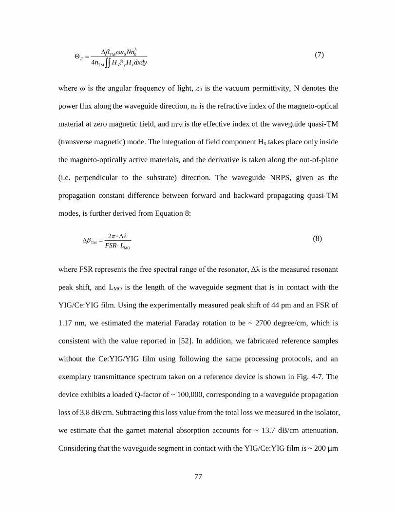
77
3
TM 0 0
TM4F
x y x
Nn
n H H dxdy
(7)
where ω is the angular frequency of light, ε0 is the vacuum permittivity, N denotes the
power flux along the waveguide direction, n0 is the refractive index of the magneto-optical
material at zero magnetic field, and nTM is the effective index of the waveguide quasi-TM
(transverse magnetic) mode. The integration of field component Hx takes place only inside
the magneto-optically active materials, and the derivative is taken along the out-of-plane
(i.e. perpendicular to the substrate) direction. The waveguide NRPS, given as the
propagation constant difference between forward and backward propagating quasi-TM
modes, is further derived from Equation 8:
TM
MO
2
FSR L
(8)
where FSR represents the free spectral range of the resonator, Δλ is the measured resonant
peak shift, and LMO is the length of the waveguide segment that is in contact with the
YIG/Ce:YIG film. Using the experimentally measured peak shift of 44 pm and an FSR of
1.17 nm, we estimated the material Faraday rotation to be ~ 2700 degree/cm, which is
consistent with the value reported in [52]. In addition, we fabricated reference samples
without the Ce:YIG/YIG film using following the same processing protocols, and an
exemplary transmittance spectrum taken on a reference device is shown in Fig. 4-7. The
device exhibits a loaded Q-factor of ~ 100,000, corresponding to a waveguide propagation
loss of 3.8 dB/cm. Subtracting this loss value from the total loss we measured in the isolator,
we estimate that the garnet material absorption accounts for ~ 13.7 dB/cm attenuation.
Considering that the waveguide segment in contact with the YIG/Ce:YIG film is ~ 200 µm

78
in length in a resonator and that the modal confinement factor in the YIG/Ce:YIG film is
15.9% (calculated using a finite difference mode solver), the material attenuation of
polycrystalline Ce:YIG/YIG was estimated to be approximately 270 dB/cm.
Total loss in the nonreciprocal resonator is computed from the measured loaded Q-factor
and extinction ratio to be 17.5 dB/cm, representing over 70% reduction compared to our
prior report [6]. Propagation loss of GeSbSe racetrack resonators without the underlying
magneto-optical oxide layers but with an otherwise identical configuration was
experimentally assessed to be 3.8 dB/cm, among which 1.1 dB/cm is attributed to scattering
losses at the four straight-to-bend junctions in the racetrack resonator according to our
finite-difference time-domain (FDTD) simulations. Such scattering losses can be easily
eliminated by replacing the circular segments in the racetrack with a curve that has a
continuous curvature change along its length, such as Euler spiral or Bezier curve [77, 78].
The remaining 2.7 dB/cm, presumably resulting from sidewall roughness scattering in the
GeSbSe waveguide, is higher than the 0.5 dB/cm loss value we previously measured in
ChG micro-ring resonators [67], indicating considerable room for further performance
improvement. Loss caused by optical absorption in the magneto-optical oxide films is
therefore 13.7 dB/cm, corresponding to 270 dB/cm absorption in the magneto-optical
oxides. This figure is considerably higher than loss we previously measured in
polycrystalline Ce:YIG films (40 dB/cm at 1550 nm [62]). We thus anticipate that the IL
of monolithic on-chip isolators can be further minimized with optimized garnet deposition
protocols to bring their performance to a level on par with or even superior to their bulk
counterparts.

79
Figure. 4-7. Transmittance spectrum of a strip loaded GeSbSe racetrack resonator on a SiO2
substrate with vertical tapers.
4.6 TE MO isolators
Besides insertion loss and isolation ratio, polarization diversity is another consideration for
isolator device design. This is particularly the case for NRPS-based devices, which to date
almost exclusively adopt a waveguide design similar to the one shown in Figure 4-3b. The
deposited MO film on top of the waveguide core breaks the structural symmetry in the out-
of-plane direction and induces NRPS for the quasi-transverse magnetic (TM) polarized
modes. On the other hand, the structure’s in-plane symmetry indicates a vanishing NRPS
for the quasi-transverse electric (TE) polarized modes. Most integrated photonic devices,
however, operate with quasi-TE polarization. The polarization mismatch can be handled

80
by adding on-chip polarization splitters and converters to transform the TM modes into TE
modes. [79] A second solution involves coating MO materials on one waveguide sidewall
to lift the in-plane symmetry for TE mode isolation. The latter scheme was recently
implemented (Figure 4-3d) by forming an amorphous silicon waveguide adjacent to a
patterned mesa of MO garnet grown on a garnet substrate. [21] Angled deposition of MO
thin films through windows opened in a thick cladding layer offers another possible route
for TE mode isolators.
SiN is another standard waveguide material widely employed in silicon photonics
platforms offering unique advantages such as back-end-of-line (BEOL) compatibility and
visible light transparency over Si. To date, integrated optical isolators have not yet been
demonstrated on the SiN platform [59]. Here we further show that our monolithic approach
can be equally applied to isolator integration on SiN through demonstration of the first TE-
mode isolator on SiN. The isolator comprises a SiN racetrack resonator encapsulated in
SiO2 cladding. A window are opened in the cladding to expose one waveguide sidewall.
The fabricated device is shown in Figs. 4-8a (top-view optical micrograph) and 4-8c (cross-
sectional SEM). It worth noting that unlike the TM resonator isolator design demonstrated
previously [6], the window can extend along the entire resonator without cancelling out
NRPS as the magnetic field is applied along the out-of-plane direction. In our SiN device,
the window covers the resonator device except the coupling section to avoid changing the
coupling condition to the bus waveguide. Transmittance spectra of forward and backward
propagation light are displayed in Fig. 4-8b, which yields an insertion loss of 11.5 dB and
an isolation ratio of 20.0 dB at resonance. We further repeated the measurement multiple
81
times, and the data in Fig. 4-8d consistently show a resonant peak shift of (15 ± 2) pm upon
reversing the light propagation direction. The result unambiguously validates
nonreciprocal light propagation in the SiN device.
Figure. 4-8. a) optical microscope image (top view) of as-fabricated SiN racetrack isolator.
(b) forward and backward transmission spectrum of SiN isolator, we observed a 15 pm
peak shift. (c) cross-sectional SEM image at the window region. (d) Recorded transmission
peak position of SiN racetrack isolator. The measurement was conducted by swithching
light propagation direction for 5 times consecutively.
The loss of SiN ring resonator can be extracted from its Q quality factor following the
analysis protocol we previously established [6]. We measured the transmission spectra of
(c)
(d)

82
this device before and after MO oxide deposition, yielding a loaded Q factor of ~45,000
and 11,000, respectively. Corresponding to a total propagation loss of 4.2 dB/cm and 17.0
dB/cm. The excess 12.8 dB/cm loss comes solely from MO oxide material absorption.
Taking account a modal confinement of 5.4% and again assuming YIG and CeYIG are
equally lossy. The MO oxide material loss is extracted to be 237 dB/cm. In our device
design, we have added an adiabatic taper to minimize scatting losses from the window.
Therefore, the only junction loss we have is the mode mismatch scattering when light
propagate between straight regions to bended regions. The loss is simulated by
FIMMPROP software and estimated to be 0.6 dB/cm. As we have a large bending radius
of 150 μm, bending loss is <0.01 dB/cm and can be neglected. Meanwhile, we extrapolated
the NRPS of MO oxide film from the peak shift and estimated to be ~ -1400 degree/cm. It
is worth noting that the NRPS of sidewall deposited MO oxide exhibited only half of the
FR than that was grown on a planar substrate. It is important to develop a deposition
technology that achieves higher NRPS of MO oxide at the sidewall to further improve
device performance.
4.7 Discussion and outlook
Performance metrics of on-chip magneto-optical isolators are summarized in Table 2. Our
TM device simultaneously claims the smallest footprint, the lowest insertion loss, as well
as the highest extinction ratio among monolithic magneto-optical isolators demonstrated
thus far and our TE device claim to be the first experimental demonstration of NRPS based
MO isolator.

83
For both Faraday rotators and NRPS-based isolators, performance is ultimately dictated by
the FOM of the MO material. For Faraday rotators, the insertion loss (IL) is given by:
45 / FOM in dBIL . (6)
For NRPS-based isolators, the waveguide design affects the NRPS (measured by phase
delay per unit waveguide length in degrees/cm) and device performance as well. Figure 4-
9c plots the ratio of waveguide NRPS and the MO material’s Faraday rotation (both with
the unit of degrees/cm) in an SOI waveguide capped with an MO thin film whose mode
profile and cross-sectional configuration are illustrated in Figure 4-9 a–b, respectively.
Table 2. Performance metrics of on-chip magneto-optical isolators
Device structure Monolithic
integration? Device length (mm) Insertion loss (dB) Isolation ratio (dB)
This work Resonator Y 0.29 3 40
Bi et al. [6] Resonator Y 0.29 18.8 19.5
Sun et al. [8] Resonator Y 0.29 7.4 13.0
Zhang et al. [11]
Faraday rotator Y 4.1 4 11
Shoji et al. [12]
Interferometer N 4.0 8 21
Ishida et al. [13]
Interferometer N > 2 10 17.9
Ghosh et al. [15]
Interferometer N ~ 2 8 - 9 14
Ghosh et al. [16]
Interferometer N 1.5 ~ 8 11
Tien et al. [17]
Resonator N 2 N/A 9
Huang et al. [18]
Resonator N 0.05 10.1 - 14.3 14.4
Huang et al. [19]
Interferometer N 1 9 - 11 29

84
Note that for all waveguide dimensions, the waveguide NRPS is less than the material’s
Faraday rotation.
Figure 4-9d presents the ILs of three types of isolator devices (Faraday rotators, MZIs, and
micro-rings, where the latter two are both based on NRPS) versus the material FOM. Here
the devices considered are ideal—for example, the only source of optical loss results from
MO material attenuation, and birefringence of the rotator is assumed to vanish. A
semistandard SOI waveguide with dimensions of 450 nm (width) × 220 nm (height) is used
for the MZI and microring devices. In all cases, the isolation ratio can, in theory, reach
infinity (e.g., for a critically coupled micro-ring or for a power-balanced MZI), and
therefore, IL is the proper device performance measure. Figure 9d indicates that Faraday
rotators offer the best-in-class performance for a given MO material FOM, provided that
their sensitivity to birefringence is properly addressed. This is a direct consequence of the
less-than-unity ratio between waveguide NRPS and material Faraday rotation shown in
Figure 4-9c.
Figure 4-9d allows us to project the performances of monolithic isolators based on
available deposited MO thin films. Reliable quantification of FOM can be challenging as
accurate loss evaluation in low-attenuation (k < 10–3) MO thin films is only possible using
waveguide measurements. Taking the best experimentally assessed loss data of 40 dB/cm56
and Faraday rotation of 2650 degrees/cm45 in PLD-deposited Ce:YIG films, we obtain a
material FOM of 66 degrees/dB. The metric corresponds to ILs of 0.11 dB (micro-ring),
0.54 dB (Faraday rotator), and 1.1 dB (MZI). The result highlights the viability of

85
achieving high-performance optical isolation based on monolithically deposited MO thin
films.
Figure 4-9. (a) Quasi-transverse magnetic (TM) mode profile and (b) cross-sectional structure of
a magneto-optical (MO)-film capped silicon-on-insulator (SOI) waveguide; (c) ratio of waveguide
nonreciprocal phase shift and the Faraday rotation of the MO material in the SOI waveguide
illustrated in (b); the dotted line delineates the waveguide single-mode (left) and multi-mode (right)
regimes. (d) Simulated insertion losses of isolators versus the MO material figure of merit (FOM).
Three different device configurations: micro-ring, Faraday rotator, and Mach–Zehnder
interferometers (MZI) are compared. Here, the micro-ring and MZI isolators consist of SOI
waveguides shown in (b) with a core width of 450 nm and a height of 220 nm. The dotted line
corresponds to the best experimentally assessed FOM in deposited cerium-doped yttrium iron
garnet (Ce:YIG) films.

86
4.8 Conclusion
In this work, we have significantly advanced the state-of-the-art in monolithic integrated
optical isolators by demonstrating an on-chip isolator with a record low insertion loss of
3.0 dB and an isolation ratio of 40 dB. The exceptional isolation performance stems from
a novel device architecture combining a strip-loaded waveguide configuration with an
adiabatic vertical taper, which effectively eliminates parasitic optical losses due to
secondary phase absorption and junction scattering while at the same time boosting
waveguide nonreciprocity. In addition, we demonstrated the first NRPS based TE isolator
with 11.5 dB insertion loss and 20 dB isolation ratio. The high-performance, all-passive
on-chip isolator constitutes a critical step towards planar integration of optical isolation
devices with large-scale photonic circuits.

87
Reference
(1) D. Jalas, A. Petrov, M. Eich, W. Freude, S. Fan, Z. Yu, R. Baets, M. Popović, A. Melloni, and J. D. Joannopoulos, Nature Photonics
7, 579 (2013).
(2) H. Dötsch, N. Bahlmann, O. Zhuromskyy, M. Hammer, L. Wilkens, R. Gerhardt, P. Hertel, and A. F. Popkov, Journal of the Optical
Society of America B-Optical Physics 22, 240-253 (2005).
(3) B. J. Stadler, and T. Mizumoto, IEEE Photonics Journal 6, 1-15 (2014).
(4) L. Bi, J. Hu, P. Jiang, H. S. Kim, D. H. Kim, M. C. Onbasli, G. F. Dionne, and C. A. Ross, Materials 6, 5094-5117 (2013).
(5) Y. Shoji, and T. Mizumoto, Science and Technology of Advanced Materials 15, 014602 (2014).
(6) L. Bi, J. Hu, P. Jiang, D. H. Kim, G. F. Dionne, L. C. Kimerling, and C. Ross, Nature Photonics 5, 758-762 (2011).
(7) L. Bi, J. Hu, L. Kimerling, and C. Ross, "Fabrication and characterization of as2s3/y3fe5o12 and y3fe5o12/soi strip-loaded waveguides
for integrated optical isolator applications," in Integrated Optics: Devices, Materials, and Technologies XIV(International Society for
Optics and Photonics2010), p. 760406.
(8) X. Y. Sun, Q. Du, T. Goto, M. C. Onbasli, D. H. Kim, N. M. Aimon, J. Hu, and C. A. Ross, ACS Photonics 2, 856-863 (2015).
(9) T. Goto, M. C. Onbasli, D. H. Kim, V. Singh, M. Inoue, L. C. Kimerling, and C. Ross, Opt. Express 22, 19047-19054 (2014).
(10) D. C. Hutchings, B. M. Holmes, C. Zhang, P. Dulal, A. D. Block, S.-Y. Sung, N. C. Seaton, and B. J. Stadler, IEEE Photonics
Journal 5, 6602512-6602512 (2013).
(11) C. Zhang, P. Dulal, B. J. Stadler, and D. C. Hutchings, Scientific Reports 7, 5820 (2017).
(12) T. Mizumoto, Y. Shoji, and R. Takei, Materials 5, 985-1004 (2012).
(13) D. Karki, V. Stenger, A. Pollick, and M. Levy, J. Appl. Phys. 121, 233101 (2017).
(14) Y. Shoji, T. Mizumoto, H. Yokoi, I.-W. Hsieh, and R. M. Osgood Jr, Appl. Phys. Lett. 92, 071117 (2008).
(15) S. Ghosh, S. Keyvavinia, W. Van Roy, T. Mizumoto, G. Roelkens, and R. Baets, Opt. Express 20, 1839-1848 (2012).
(16) S. Ghosh, S. Keyvaninia, Y. Shoji, W. Van Roy, T. Mizumoto, G. Roelkens, and R. G. Baets, IEEE Photonics Technology Letters
24, 1653-1656 (2012).
(17) M.-C. Tien, T. Mizumoto, P. Pintus, H. Kromer, and J. E. Bowers, Opt. Express 19, 11740-11745 (2011).
(18) D. Huang, P. Pintus, C. Zhang, P. Morton, Y. Shoji, T. Mizumoto, and J. E. Bowers, Optica 4, 23-30 (2017).
(19) D. Huang, P. Pintus, Y. Shoji, P. Morton, T. Mizumoto, and J. E. Bowers, Opt. Lett. 42, 4901-4904 (2017).
(20) D. Huang, P. Pintus, C. Zhang, Y. Shoji, T. Mizumoto, and J. E. Bowers, IEEE Journal of Selected Topics in Quantum Electronics
22, 271-278 (2016).
(21) E. Ishida, K. Miura, Y. Shoji, H. Yokoi, T. Mizumoto, N. Nishiyama, and S. Arai, Opt. Express 25, 452-462 (2017).
(22) J. Montoya, K. Parameswaran, J. Hensley, M. Allen, and R. Ram, J. Appl. Phys. 106, 023108 (2009).
(23) H. Shimizu, and Y. Nakano, IEEE Photonics Technology Letters 19, 1973-1975 (2007).
(24) M. Levy, T. K. Carroll, and R. El-Ganainy, Opt. Lett. 40, 111-114 (2015).
(25) Y. Shi, Z. Yu, and S. Fan, Nature Photonics 9, 388-392 (2015).
(26) L. Fan, J. Wang, L. T. Varghese, H. Shen, B. Niu, Y. Xuan, A. M. Weiner, and M. Qi, Science 335, 447-450 (2012).

88
(27) L. Chang, X. Jiang, S. Hua, C. Yang, J. Wen, L. Jiang, G. Li, G. Wang, and M. Xiao, Nature Photonics 8, 524 (2014).
(28) B. Peng, Ş. K. Özdemir, F. Lei, F. Monifi, M. Gianfreda, G. L. Long, S. Fan, F. Nori, C. M. Bender, and L. Yang, Nature Physics
10, 394 (2014).
(29) L. Del Bino, J. M. Silver, M. T. Woodley, S. L. Stebbings, X. Zhao, and P. Del’Haye, Optica 5, 279-282 (2018).
(30) Z. Yu, and S. Fan, Nature Photonics 3, 91 (2009).
(31) H. Lira, Z. Yu, S. Fan, and M. Lipson, Phys. Rev. Lett. 109, 033901 (2012).
(32) Y. Yang, C. Galland, Y. Liu, K. Tan, R. Ding, Q. Li, K. Bergman, T. Baehr-Jones, and M. Hochberg, Opt. Express 22, 17409-
17422 (2014).
(33) C. Doerr, L. Chen, and D. Vermeulen, Opt. Express 22, 4493-4498 (2014).
(34) S. Manipatruni, J. T. Robinson, and M. Lipson, Phys. Rev. Lett. 102, 213903 (2009).
(35) T. Shintaku, A. Tate, and S. Mino, Appl. Phys. Lett. 71, 1640-1642 (1997).
(36) H. Hemme, H. Dötsch, P. Hertel, Appl. Opt. 29, 2741 (1990).
(37) L. Tang, S. Drezdzon, T. Yoshie, Opt. Express 16, 16202 (2008).
(38) R. El-Ganainy, P. Kumar, M. Levy, Opt. Lett. 38, 61 (2013).
(39) J. Montoya, K. Parameswaran, J. Hensley, M. Allen, R. Ram, J. Appl. Phys. 106, 023108 (2009).
(40) J. Hammer, G. Ozgur, G. Evans, J. Butler, J. Appl. Phys. 100, 103103 (2006).
(41) H. Yokoi, T. Mizumoto, Y. Shoji, Appl. Opt. 42, 6605 (2003).
(42) J. Fujita, M. Levy, R. Osgood, L. Wilkens, H. Dötsch, Appl. Phys. Lett. 76, 2158 (2000).
(43) Y. Shoji, T. Mizumoto, Opt. Express 15, 639 (2007).
(44) N. Kono, K. Kakihara, K. Saitoh, M. Koshiba, Opt. Express 15, 7737 (2007).
(45) H. Zhu, C. Jiang, J. Lightwave Technol. 29, 1647 (2011).
(46) J. Yang, J. Roh, S. Ok, D. Woo, Y. Byun, W. Lee, T. Mizumoto, S. Lee, IEEE Trans. Magn. 41, 3520 (2005).
(47) K. Shui, L. Nie, Y. Zhang, B. Peng, J. Xie, L. Deng, L. Bi, Opt. Express 24, 12856 (2016).
(48) N. Kono, M. Koshiba, Opt. Express 13, 9155 (2005).
(49) T. Boudiar, B. Payet-Gervy, M.-F. Blanc-Mignon, J.-J. Rousseau, M. Le Berre, H. Joisten, J. Magn. Magn. Mater. 284, 77 (2004).
(50) S. Sung, X. Qi, B. Stadler, Appl. Phys. Lett. 87, 121111 (2005).
(51) S. Sung, X. Qi, B. Stadler, in Conference on Lasers and Electro-Optics (Optical Society of America, 2007), p. CThN5.
(52) M. Onbasli, L. Beran, M. Zahradník, M. Kučera, R. Antoš, J. Mistrík, G. Dionne, M. Veis, C. Ross, Sci. Rep. 6, 23640 (2016).
(53) J. Hu, X. Sun, Q. Du, M. Onbasli, C. Ross, Proc. SPIE (2016), vol. 9750, p. 97500W-1.
(54) B. Stadler, T. Mizumoto, IEEE Photon. J. 6, 1 (2014).
(55) P. Hansen, J. Krumme, Thin Solid Films 114, 69 (1984).
(56) M.C. Onbasli, T. Goto, X. Sun, N. Huynh, C.A. Ross, Opt. Express 22 (21), 25183 (2014).
(57) P. Dulal, A. Block, T. Gage, H. Haldren, S. Sung, D. Hutchings, B. Stadler, ACS Photonics 3, 1818 (2016).
(58) "Ir free-space isolators," https://www.thorlabs.com/newgrouppage9.cfm?objectgroup_id=4916.
(59) M. C. Onbasli, T. Goto, X. Sun, N. Huynh, and C. Ross, Opt. Express 22, 25183-25192 (2014).
89
(60) T. Shintaku, A. Tate, and S. Mino, Appl. Phys. Lett. 71, 1640-1642 (1997).
(61) M. C. Onbasli, L. Beran, M. Zahradník, M. Kučera, R. Antoš, J. Mistrík, G. F. Dionne, M. Veis, and C. A. Ross, Scientific Reports
6, 23640 (2016).
(62) L. Bi, J. Hu, G. F. Dionne, L. Kimerling, and C. Ross, "Monolithic integration of chalcogenide glass/iron garnet waveguides and
resonators for on-chip nonreciprocal photonic devices," in Integrated Optics: Devices, Materials, and Technologies XV(International
Society for Optics and Photonics2011), p. 794105.
(63) T. Goto, M. C. Onbaşlı, and C. A. Ross, Opt. Express 20, 28507-28517 (2012).
(64) S.-Y. Sung, A. Sharma, A. Block, K. Keuhn, and B. J. H. Stadler, J. Appl. Phys. 109, 07B738 (2011).
(65) W.-H. Wei, R.-P. Wang, X. Shen, L. Fang, and B. Luther-Davies, The Journal of Physical Chemistry C 117, 16571-16576 (2013).
(66) M. R. Krogstad, S. Ahn, W. Park, and J. T. Gopinath, Opt. Express 23, 7870-7878 (2015).
(67) Q. Du, Y. Huang, J. Li, D. Kita, J. Michon, H. Lin, L. Li, S. Novak, K. Richardson, and W. Zhang, Opt. Lett. 41, 3090-3093 (2016).
(68) Q. Du, Z. Luo, H. Zhong, Y. Zhang, Y. Huang, T. Du, W. Zhang, T. Gu, and J. Hu, Photonics Research 6, 506-510 (2018).
(69) L. Li, H. Lin, Y. Huang, R.-J. Shiue, A. Yadav, J. Li, J. Michon, D. Englund, K. Richardson, and T. Gu, Optica 5, 44-51 (2018).
(70) H. Lin, Y. Song, Y. Huang, D. Kita, S. Deckoff-Jones, K. Wang, L. Li, J. Li, H. Zheng, and Z. Luo, Nature Photonics 11, 798-805
(2017).
(71) L. Li, H. Lin, S. Qiao, Y. Zou, S. Danto, K. Richardson, J. D. Musgraves, N. Lu, and J. Hu, Nature Photonics 8, 643-649 (2014).
(72) J. Hu, L. Li, H. Lin, Y. Zou, Q. Du, C. Smith, S. Novak, K. Richardson, and J. D. Musgraves, Am. Ceram. Soc. Bull. 94, 24-29
(2015).
(73) J. F. Bauters, M. J. Heck, D. John, D. Dai, M.-C. Tien, J. S. Barton, A. Leinse, R. G. Heideman, D. J. Blumenthal, and J. E. Bowers,
Opt. Express 19, 3163-3174 (2011).
(74) S. K. Selvaraja, E. Sleeckx, M. Schaekers, W. Bogaerts, D. Van Thourhout, P. Dumon, and R. Baets, Opt. Commun. 282, 1767-
1770 (2009).
(75) T. E. Dillon, A. Sure, J. A. Murakowski, and D. W. Prather, Journal of Micro/Nanolithography, MEMS, and MOEMS 3, 550-555
(2004).
(76) Y. Zhang, C. Wang, X. Liang, B. Peng, H. Lu, P. Zhou, L. Zhang, J. Xie, L. Deng, and M. Zahradnik, J. Alloys Compd. 703, 591-
599 (2017).
(77) M. Cherchi, S. Ylinen, M. Harjanne, M. Kapulainen, and T. Aalto, Opt. Express 21, 17814-17823 (2013).
(78) L. Li, H. Lin, S. Qiao, Y.-Z. Huang, J.-Y. Li, J. Michon, T. Gu, C. Alosno-Ramos, L. Vivien, and A. Yadav, Light: Science &
Applications 7, 17138 (2018)
(79) D. Dai, J. Bauters, J.E. Bowers, Light Sci. Appl. 1, e1 (2012).

90
Chapter 5. Radiation Induced Effects in Silicon Photonic
Materials and Devices
5.1 Radiation Overview
Understanding radiation damage is of significant importance for devices operating in
radiation-harsh environments. High energy radiation tends to create defects in materials
and thereby modify their electronic and optical properties. Mitigating radiation-induced
damage associated with such defect generation is an important design consideration for
devices used in outer space, near nuclear reactors, or close to particle colliders. As satellite
communications and data links for next-generation particle accelerators start turning to
integrated photonics solutions, [1] the demand to understand radiation-induced degradation
mechanisms in photonic devices becomes critical. In nuclear and space environment,
radiation includes alpha ray (He ions), beta ray (electrons), gamma ray (photons) and
neutrons. In general, radiation damage can be categorized into two types, ionization
damage and displacement damage. Ionization dose produces density and polarization
variation as well as free carrier accumulation in materials which shifts material refractive
index and losses. This type of damage is usually caused by fast moving charged particles
and photons. While displacement damage creates defects in mid gap, contributing to a
modification of charge trapping and carrier lifetime, thus changes material optical
properties, and heavy ions bombardment tends to create such effects.

91
In crystalline optical materials such as silicon on insulator (SOI), optical property changes
occur through both ionization damage and displacement damage [2]. Ionization leads to
free carriers which modify refractive index and optical absorption via the plasma dispersion
effect. Ionization damage also creates trapped charges at the Si/SiO2 interface which likely
accounts for the phase drift observed in SOI modulators [3]. Displacement damage results
in lattice defects which impacts optical properties through local polarizability change and
carrier density modulation due to trap states. Gamma radiation-induced effects in SOI have
been characterized by both in-situ [4] and ex-situ [5] measurements using optical resonator
devices. Besides the aforementioned bulk material structural transformations, surface
oxidation was identified as a contributor to observed resonance spectral shift [5].
In this chapter, we first discuss simulation method and show preliminary results from alpha
radiation on silicon nitride samples. Then detailed quantitative study is conducted for
gamma radiation on a-Si, SiNx and SiC materials and devices. The origin of the observed
device behavior modification is also discussed.
5.2 Stopping Range of Ions in Mater (SRIM)
Even though the energy of the alpha particles is comparable to that of the Co60 gamma rays,
the nature of the two radiations is fundamentally different. Alpha particles can create
damage cascades due to their high mass which creates areas with high densities of defects.
The mechanism of interaction of the alpha particles with the lattice atoms is twofold. First,
the ion is too energetic to directly interact with the nuclei, but due to its positive charge, it

92
strongly interacts with the electron cloud of the semiconductor losing energy and creating
defects at a constant rate. This is known as the electronic stopping phase. Once it has
0 20 40 60 80 1000
500
1000
1500
2000
2500
3000
3500
4000
4500
Pro
jecte
d R
an
ge
(A
ms
tro
ng
)
Ion Energy (KeV)
Projected Range
Figure 5-1 – Stopping range plot of alpha particles with different energies.
slowed down enough, the ion starts colliding with nuclei, losing its energy very quickly
creating cascaded damage (the knocked-out nucleus can further displace other nuclei). This
is known as the nuclear stopping phase, during which the ion loses all of its remaining
energy very quickly. Due to these two stopping mechanisms, the damage in the irradiated
material is not homogeneously distributed; the defect concentration increases slightly in
the electronic stopping region (which is of the order of a micrometer long depending on
the initial energy), peaks in the nuclear stopping region (also called end of range (EOR)
which is around 100 nanometers long in our experiments). After the end of range, no
defects are produced anymore. We used the software “Stopping and Ion Range in Matter”
(SRIM) to simulate the damage distribution so that we could determine the optimal

93
irradiation energy for our experiments. Figure 5-1 shows alpha particle (helium ion)
stopping range in silicon nitride. Detailed damage is calculated and shown in Figure 5-2.
The ionization energy loss rate as the particles penetrate into the material is described by
Linear Energy Transfer function (LET) while the displacement damage event is reflected
0 2000 4000 6000 8000 100000
5
10
15
20
25
30
35
LE
T (
ev / io
n / A
mstr
on
g)
Target Depth (Amstrong)
100KeV
80KeV
60KeV
40KeV
20KeV
0 2000 4000 6000 8000 100000
1
2
3
4
5
NIE
L (
eV
/ A
ms
tro
ng
)
Target Depth (Amstrong)
20KeV
40KeV
60KeV
80KeV
100KeV

94
Figure 5-2 – LET and NIEL of alpha particle damage with energies ranging from 20KeV to
100KeV on silicon nitride film. From the simulation, we conclude that for silicon nitride device
with 400 nm thickness, alpha irradiation with energy of ~60 keV should be chosen in our irradiation
experiments as it can induce most damage inside the material, and can yield insights into the upper
and lower limits for rad-hardness.
by Non-Ionization Energy Loss (NIEL). The energy range from 20 keV to 100 keV is used
for the calculation.
From the simulation, we conclude that for silicon nitride device with 400 nm thickness,
alpha irradiation with energy of ~60 keV should be chosen in our irradiation experiments
as it can induce most damage inside the material, and can yield insights into the upper
and lower limits for rad-hardness.
Optical resonator devices were used to evaluate the radiation induced optical property
modification of the materials and the impact on photonic device performance. The devices
were fabricated using the following steps: a 400 nm thick silicon nitride film was first
deposited onto silicon wafer with 3 m thermal oxide on top. SPR-700 photoresist was
then spin-coated and an i-line stepper was used to pattern 800 nm wide waveguide
resonator. The as-patterned silicon nitride films were patterned in a Reactive Ion Etching
(RIE) plasma etcher. An equal amount of CHF3 and CF4 gas mixture was flowed into the
chamber to transfer the pattern into the silicon nitride. Finally, residual photoresist was
removed by putting the chip into a piranha solution (75% H2SO4 + 25% H2O2).

95
Transmission spectrum of the resonators were measured via a fiber butt coupling method.
A tunable laser of wavelength ranging from 1500 nm to 1600 nm was used as the light
source. The optical resonators were measured before and after irradiation and their
temperature was controlled within less than 0.2 ℃.
The radiation was carried out in PNNL at an alpha irradiator with an energy of 5MeV.
Figure 5-3 shows the transmission spectra of alpha irradiated resonators. The large resonant
shifts indicate that it is mandatory to protect SiN resonators against surface oxidation if
they were used in a radiation environment.
1520 1530 1540 1550 1560
0.0
1.0x10⁻⁷
2.0x10⁻⁷
3.0x10⁻⁷
4.0x10⁻⁷
5.0x10⁻⁷
6.0x10⁻⁷
7.0x10⁻⁷
8.0x10⁻⁷
Tra
nsm
itta
nce
Wavelength / nm
after irradiation
before irradiation
Figure 5-3 – Transmission spectra of silicon nitride resonators before and after alpha irradiation

96
5.3 Gamma Radiation Damage in a-Si and SiNx Materials and Devices
In this study, we focus on gamma radiation-induced effects in amorphous silicon (a-Si) and silicon
nitride (SiNx) photonic devices. Both a-Si and SiNx have low optical loss near 1550 nm
telecommunication wavelength [6]. For instance, SiNx waveguides with a remarkably low optical
loss down to 0.045 dB/m have been demonstrated [7]. Their amorphous nature and compatibility
with standard Si CMOS processing also qualify them as promising candidates for back end of line
(BEOL) photonic integration [8]. Additionally, both materials exhibit large Kerr coefficients useful
for nonlinear optical applications [9,10].
Radiation damage in a-Si has been investigated in electronic devices including field effect
transistors [11], photodetectors [12] and solar cells [13]. In electronic devices, it was concluded that
ionization damage is the primary degradation mechanism [14]. For passive photonic applications,
however, bulk optical property changes in a-Si are likely dictated by atomic structural perturbations
resulting from displacement defects. This is different from the case of crystalline silicon, because
free carrier effects (plasma dispersion and free carrier absorption) are minimal in a-Si given its
small carrier mobility. Likewise, we anticipate that displacement is the main damage mechanism
in SiNx materials.
On the experimental side, radiation effects on a-Si and SiNx photonic devices have only been
reported in a few recent studies. Grillanda et al. studied gamma radiation damage in a-Si resonators
covered with a silicon dioxide cladding grown by chemical vapor deposition (CVD) and found
minimal resonance shift up to 15 Mrad absorbed dose [15]. This observation is likely a
consequence of cladding compensation as CVD silicon dioxide exhibits a negative refractive index

97
change upon gamma ray exposure. In nitride devices, proton irradiation up to a total fluence of ~
1010 protons/cm2 produced negligible loss change [16]. In silicon oxynitride waveguides, a large
index change in the order of 0.01 was measured upon exposure to alpha radiation [17].
Figure 5-4. (a) Top-view optical microscope image of an a-Si micro-ring resonator; (b)
transmission spectra of the a-Si resonator before (black curve) and after (red curve) receiving 2
Mrad gamma irradiation
The present work aims to provide a precise, quantitative measurement of total dose effect of gamma
irradiation on a-Si and SiNx photonic devices. Radiation-induced optical property modifications
are evaluated using micro-ring resonators. Refractive index change of a-Si and SiNx can be
calculated from the resonant peak shift whereas optical absorption increase, if any, is inferred from
the extinction ratio change [18]. The irradiated a-Si and SiNx materials were also characterized by
high resolution transmission electron microscopy (HRTEM), grazing incidence X-ray diffraction
(XRD), and X-ray photoelectron Spectroscopy (XPS) to elucidate the underlying structural
transformation mechanisms responsible for the observed optical property modifications.

98
Fabrication of a-Si and SiNx resonators followed the standard Si microfabrication processes. Thin
film a-Si and silicon nitride was first deposited onto silicon wafers with 3 μm thermal oxide using
plasma enhanced chemical vapor deposition (PECVD) and low pressure chemical vapor
deposition (LPCVD), respectively. The SiNx film has a refractive index of 2.1 at 1550 nm
wavelength (compared to an index of 2.0 for stoichiometric Si3N4) and is thus silicon-rich. The a-
Si devices were patterned using electron beam lithography, whereas photolithography performed
on an i-line stepper was used to define the SiNx device structures. Subsequently, the patterns were
transferred to the film by reactive ion etch with Cl2 for a-Si and a mixture of CF4 and CHF3 gases
for nitride. The as-fabricated a-Si waveguide has dimensions of 450 nm (width) by 250 nm (height),
and SiNx waveguide has a cross section of 800 nm × 400 nm. Figure 5-4a shows the top view of
an a-Si resonator used in our experiment.
Optical transmission spectrum of the devices was characterized on a Newport Auto Align
workstation equipped with an optical vector analyzer (LUNA Technologies OVA-5000) and a
built-in tunable laser. Near-infrared light was coupled in and out of the resonators through bus
waveguides using tapered lens-tip fibers. The loaded quality factors (Q-factors) of as-fabricated a-
Si and SiNx resonators are both around 105.
Gamma irradiation of the devices was conducted using a Co-60 source with photon energies of
1.17 MeV and 1.33 MeV. For the experiments described herein, every as-fabricated device chip
was diced into two nominally identical pieces. One of them (the “sample“) was exposed to gamma
irradiation while the other (the “reference”) was kept in an otherwise identical environment (i.e. at
the same temperature, humidity, and lighting conditions). Post-irradiation measurements were

99
performed with the devices mounted on a thermostat stage maintained at a constant temperature of
(19.7 ± 0.2) °C. The radiation-induced resonance shift Δλ is calculated via:
0 0, 1 1, ,r r (1)
where λ0 and λ1 denote the resonant wavelengths of the sample before and after gamma irradiation,
and λ0,r and λ1,r are the resonant wavelengths of the reference measured under identical conditions.
The use of a reference chip allows us to eliminate environmental noise interfering with precise
index quantification. In the experiments, we can reliably measure index change down to 2 × 10⁻⁶
in SiNx and 5 × 10⁻⁵ in a-Si, with the measurement accuracy ultimately limited by temperature
stability of the thermostat stage. Fig. 5-4b plots an example of device transmission spectra for an a-
Si resonator prior to and after exposure to 2 Mrad gamma irradiation (dose calibrated to silicon).
The extinction ratio and Q-factor remain unchanged, signaling negligible loss increase after gamma
irradiation. To ascertain that the thermal oxide undercladding does not contribute significantly to
the observed peak shift, we quantified the refractive indices of thermal oxide films before and after
gamma irradiation using variable angle spectroscopic ellipsometry (VASE). The ellipsometry
measurement consistently yielded identical indices for thermal oxide before and after gamma
irradiation doses up to 20 Mrad. Standard deviation of the index measurement is less than 2 × 10⁻⁴.
Considering that the modal confinement factor in the undercladding is only about 6% and 23% in
a-Si and SiNx devices, respectively, we conclude that the contribution from thermal oxide to the
post-irradiation resonance shift is insignificant.

100
Figure 5-5. HRTEM images of a-Si sample before (a) and after (b) 20 Mrad radiation. (c) and (d) are the
corresponding images of a SiNx film before and after radiation under same dose. (e) and (f): XRD spectra of
a-Si and SiNx thin film before and after 20 Mrad gamma irradiation, respectively.

101
HRTEM images (shown in Fig. 5-5) were taken on a-Si and SiNx films before and after irradiation.
The HRTEM samples were prepared by ion milling to obtain a ~20 nm thick lamella for imaging.
Images before (Figs. 5-5a and 5-5c) and after (Figs. 5-5b and 5-5d) receiving 20 Mrad radiation
dose do not exhibit discernable structural differences. No signs of crystallization were found after
examining >10 HRTEM images. The absence of radiation-induced crystallization is further
confirmed by the XRD spectra plotted in Figs. 5-5e and 5-5f, where no sharp diffraction peaks
were identified after irradiation. The results exclude radiation-induced crystallization found in
several amorphous material systems including a-Si [19-21] as a possible mechanism for the
observed refractive index increase.
While HRTEM and XRD do not reveal clear signatures of radiation effects, XPS analysis shows
surface chemistry modification as a result of gamma irradiation. Figure 5-6a plots the XPS
spectrum of the silicon 2p peak in as-deposited a-Si film. The spectra can be deconvolved into two
peaks, corresponding to Si-Si bonds at a binding energy of ~99 eV and Si-O bonds at ~103 eV.
Relative concentrations of the two types of bonds can be determined by comparing the areas under
the deconvolved peaks. The black curve in Fig. 5-6b plots the calculated Si-O bond fractions in as-
deposited and gamma irradiated (irradiated at 1 Mrad and 10 Mrad doses in air) a-Si films. The
increased Si-O bond fraction indicates native oxide layer growth catalyzed by gamma irradiation.
This is not surprising since highly energetic photon beams such as gamma and X-rays are known
to decompose oxygen molecules in air into reactive species such as O- and ozone, and it has been
shown that these highly reactive species contribute to accelerated surface oxide growth in
crystalline silicon [5,22]. To unequivocally identify the surface oxidation effect, we performed a
second set of irradiation experiments using samples sealed inside ultra-high-purity (oxygen

102
Figure 5-6. (a) and (c): Si 2p peak from a high resolution XPS scan of as-deposited (a) a-Si
and (c) SiNx films. The spectra are deconvoluted into different Si bonding states, where the
red curves correspond to Si-O bond, the blue curve are assigned to Si-Si bond and the pink
curves are associated with Si-N bond. The Insets show the sums of the deconvoluted peaks,
indicating good fitting quality; (b) and (d) calculated surface Si-O bond fraction for (b) a-Si
and (d) SiNx samples irradiated in argon (red) and ambient air (black).
impurity < 5 ppm) argon gas filled glass tubes. Since gamma rays are highly penetrating in glass,
the sealing tube has a minimal impact on the irradiation dose received by the sample. The Si-O
bond fraction hardly increases in the sample irradiated in argon (Fig. 5-6b), illustrating the
suppression of oxide growth. A similar trend was found in SiNx films as shown in Figs. 5-6c and

103
5-6d, which confirms that accelerated surface oxidation is also present in SiNx devices exposed to
gamma radiation in air.
Figure 5-7. Dependences of refractive index changes on cumulative gamma radiation dose
in (a) a-Si and (b) SiNx inferred from optical resonator measurements.
The impact of surface oxidation on optical resonance drift is characterized by sequentially
irradiating resonator samples multiple times with 2 Mrad dose increments up to a total cumulative
dose of 10 Mrad. Optical transmittance of the devices was collected before and after every
irradiation session. The radiation-induced resonant wavelength shift calculated from Eq. 1 was
measured in multiple (5 or more) devices, and the average spectral shift Δ𝜆̅̅̅̅ was used to infer the
core material index change via:
,g
eff
r
nn
(2)
where λr denotes the resonant wavelength, ng represents the mode group index, and ∆neff gives the
effective refractive index change of the waveguide mode. The group index ng is related to the free

104
spectrum range in the wavelength domain (FSR, defined as the spacing between two adjacent
optical resonant peaks) by:
2
,FSR
r
gnL
(3)
where L is the roundtrip length of the optical resonator. The radiation-induced index change in a-
Si and SiNx measured using this method are plotted in Fig. 5-7. The error bars in Fig. 5-7 take into
account the experimental uncertainty due to both temperature fluctuations and sample-to-sample
variations. In Fig. 5-7b, the error bars are small (< 10-5) and thus hardly visible from the plot. For
both a-Si and SiNx, their refractive indices increase monotonically with increasing radiation dose
when irradiated in argon. The index increase follows approximate linear dependences on
cumulative total radiation dose in both materials. Since the possibility of radiation-induced
crystallization is excluded, the observation suggests that densification or compaction of the
amorphous atomic network is the likely cause of the index increase [23]. In comparison, the index
increase is retarded in devices irradiated in ambient air and plateaus beyond 6 Mrad dose in a-Si.
In SiNx, its refractive index drops slightly after an initial rise at 2 Mrad dose. Since silicon dioxide
has a lower refractive index (nSiO2 = 1.45) than those of a-Si (na-Si = 3.6) and SiNx (nSiNx = 2.1), the
trend is attributed to a surface oxide formation which counteracts the index increase due to
densification.

105
5.4 Gamma Radiation Damage in a-SiC Materials and Devices
Silicon carbide (SiC) has been considered as leading candidate in radiation harsh environment due
to its strong Si-C covalent bonding. In Micro- (or Nano-) electromechanical systems, MEMS (or
NEMS), SiC exhibits advantages over other silicon based material owing to its large band gap, low
absorption in telecommunication band and high bulk modulus. In this section, we focused on
detecting radiation induced refractive index shift in SiC materials using NOMS devices as testing
vehicles. Amorphous silicon carbide (a-SiC) is chosen to be our material of interest as a-SiC can
be easily deposited on any substrate via chemical vapor deposition (CVD). As a radiation resistant
material, radiation induce effect in SiC material are notably small which can be beyond the
detection limit of conventional techniques. To improve detection capability, optical resonators are
chosen to be our testing platform as cavity enhancement allows us to detect index change to the
order of 10-5.
Fabrication of SiC devices followed the standard Si microfabrication processes. Prior to SiC growth,
a 1 μm PECVD silicon dioxide was first deposited onto silicon wafers, and then 170 nm thin film
silicon carbide was grown using the same PECVD tool. Electron beam resist ZEP 520A was
subsequently spun onto the film, forming an ~700 nm layer. The resonator pattern was written by
an Elionix electron beam lithography system at an acceleration voltage of 120 KV and a 10 nA
beam current. Subsequently, the patterns were transferred to the film by reactive ion etch (RIE)
with a mixture of CF4 and CHF3 gases. The as-fabricated silicon carbide rib waveguide has an

106
etching depth of 120 nm and varied width, ranging from 1 μm to 1.6 μm. The radius of the resonator
was chosen to be 150 μm to ensure low bending losses. Resist stripping included one hour soaking
in N-Methyl-2-pyrrolidone and sonicating for 3 minute. To ensure complete removal of resist and
fluorocarbon polymer residue formed in RIE, the device was further piranha cleaned for 10 minutes.
Finally, another 1 μm silicon oxide was deposited onto the device as an upper cladding. Figure 5-
8a shows a top view optical microscope image of a fabricated micro-ring resonator and its
corresponding waveguide mode is provided in 8b. To further observe the waveguide profile, both
top and cross section view SEM micrographs were taken and shown in Figure 5-8c and 5-8d,
respectively. The SEM images clearly indicated no etching residue was present.
Figure5- 8. (a) Optical microscope image silicon carbide micro-resonator; (b) Optical mode
of the fabricated silicon carbide waveguide with 1 μm width; SEM micrographs are shown (c)
top view and (d) cross section, respectively.

107
Optical transmission spectrum was characterized on a Newport Auto Align workstation
and an optical vector analyzer (LUNA Technologies OVA-5000) with a built-in tunable
laser. Near-infrared wavelength light was coupled in and out through the bus waveguide
using tapered lens-tip fiber. All measurements were performed at a constant temperature
Figure 5-9. (a) Transmission spectra of silicon carbide resonator before and after 2 Mrad gamma
radiation in air; (b) quantitative analysis of peak shift with respect to radiation dose; (c) linear
extrapolation of effective index change, the result shows a 0.0015 index change in silicon carbide
material after receiving 2 Mrad. (d) silicon carbide core refractive index change with radiation
dose.
a b
c d

108
of (19.7 ± 0.2) °C. The temperature stability ensures that index change down to 2 × 10⁻⁵
can be reliably measured.
The samples were irradiated multiple times with 2 Mrad increment in total dose. Figure 5-
9a illustrates the transmission spectrum of a SiC resonator near one of its resonance peaks.
A peak red shift was clearly discernable after the sample received 2 Mrad radiation. The
refractive index modification is calculated from equation 2 and 3:
The index change is plotted in Figure 5-9b. It is interesting to note that the refractive index
shifts of those devices irradiated in air exhibit a "saturated" behavior, where the peak shift
stays at the same position as dose increases. Similar trend is found in devices with different
modal confinement in SiC core. By linearly extrapolating the refractive index shift with
respect to modal confinement factor to 100%, we are able to determine the material index
change after radiation. The trend is ploted in Figure 9c. We conclude that radiation induced
refractive index change in SiC and SiO2 cladding are in the same order of magnitude but
differ in sign, where SiC tends to increase in index while SiO2 cladding index decreases.
5.6 Conclusion
In summary, we quantified for the first time (to the best of our knowledge) refractive index increase
in a-Si and SiNx materials induced by gamma irradiation through on-chip optical resonator
characterization. No measurable changes in optical loss were observed in both materials. When the
devices were irradiated in an inert (argon gas) environment, index increase in a-Si and SiNx follow
approximate linear dependence on the total radiation dose attributed to radiation-induced

109
amorphous network densification in the materials. The index increase is retarded in devices
irradiated in ambient air due to the added effect of surface oxidation confirmed by our XPS analysis.
The quantitative information on gamma radiation effects in a-Si and SiNx devices provides useful
design guidelines for photonic systems operating in radiation-harsh environments. In the meantime,
we quantified radiation induced index modification in a-SiC and we developed a technology to
separate core and cladding index modification. It worth noting that the index change of a-SiC and
SiO2 cladding are in opposite direction. We therefore are able to build gamma radiation hard
photonic devices by carefully adjust modal confinement factor to allow cancelling out the index
change contributions from core and cladding to the effective index.

110
Reference
(1) M. Zerler, SPIE Prof., October (2015)
(2) F. De Leonardis, B. Troia, C.E. Campanella, F. Prudenzano, and V.M. Passaro, IEEE Trans. Nucl. Sci. 62, 2155 (2015)
(3) S.S. El Nasr-Storey, F. Boeuf, C. Baudot, S. Detraz, J.M. Fedeli, D. Marris-Morini, L. Olantera, G. Pezzullo, C. Sigaud, C. Soos and J.
Troska, IEEE Trans. Nucl. Sci. 62, 329 (2015).
(4) P. Dumon, R. Kappeler, D. Barros, I. McKenzie, D. Doyle and R. Baets, In Optics & Photonics 2005 (International Society for Optics
and Photonics. 2005) p. 58970D
(5) S. Bhandaru, S. Hu, D.M. Fleetwood and S.M. Weiss, 2015. IEEE Trans. Nucl. Sci. 62, 323 (2015).
(6) R. Sun, J. Cheng, J. Michel and L.C. Kimerling, Opt. Lett. 34, 2378 (2009).
(7) J.F. Bauters, M.J. Heck, D.D. John, J.S. Barton, C.M. Bruinink, A. Leinse, R.G. Heideman, D.J. Blumenthal and J.E. Bowers, Opt.
Express, 19, 24090 (2011).
(8) Y.H.D. Lee and M. Lipson, IEEE J. Sel. Topics Quantum Electron., 19, 409 (2013)
(9) J.J. Wathen, V.R. Pagán, R.J. Suess, K.Y. Wang, A.C. Foster and T.E. Murphy, Opt. Express, 22, 22730 (2014)
(10) Y. Okawachi, K. Saha, J.S. Levy, Y.H. Wen, M. Lipson and A.L. Gaeta, Opt. Lett. 36, 3398 (2011)
(11) J.M. Boudry and L.E. Antonuk, 1996. Radiation damage of amorphous silicon, thin‐film, field‐effect transistors. Med. Phys., 23, 743
(1996)
(12) L.E. Antonuk, J. Boudry, J. Yorkston, C.F. Wild, M.J. Longo and R.A. Street, Nucl. Instrum. Meth. A, 299, 143 (1990)
(13) D. Nikolić, K. Stanković, L. Timotijević, Z. Rajović and M. Vujisić, Inter. J. Photoenergy (2013)
(14) J.R. Srour, G.J. Vendura, D.H. Lo, C.M.C. Toporow, M. Dooley, R.P. Nakano and E.E. King, IEEE Trans. Nucl. Sci., 45, 2624
(1998)
(15) S. Grillanda, V. Singh, V. Raghunathan, F. Morichetti, A. Melloni, L.C. Kimerling, and A.M. Agarwal, Opt. Lett. 41, 3053 (2016)
(16) V. Brasch, Q.F. Chen, S. Schiller and T.J. Kippenberg, Opt. Express, 22, 30786 (2014)
(17) F. Morichetti, S. Grillanda, S. Manandhar, V. Shutthanandan, L.C. Kimerling, A. Melloni and A.M. Agarwal, 2016. ACS Photon. 3,
1569 (2016)
(18) J. Hu, N. Carlie, L. Petit, A. Agarwal, K. Richardson, and L. C. Kimerling, J. Lightwave Technol. 27, 5240-5245 (2009)
(19) R.G. Elliman, J.S. Williams, W.L. Brown, A. Leiberich, D.M. Maher and R.V. Knoell, Nucl. Instrum. Meth. B 19, 435 (1987)
(20) M.P. Krulikovskaya, A.A. Kuzub, L.I. Chirko and A.M. Shalaev, Bull. Acad. Sci. USSR, Phys. Ser., 6, 37 (1985)
(21) H. Cui, E.T. Pashuck, Y.S. Velichko, S.J. Weigand, A.G. Cheetham, C.J. Newcomb and S.I. Stupp, Science, 327, 555 (2010))
(22) S. Bhandaru, E.X. Zhang, D.M. Fleetwood, R.A. Reed, R.A. Weller, R.R. Harl, B.R. Rogers and S.M. Weiss, IEEE Trans. Nucl.
Sci., 59, 781 (2012)
(23) F. Piao, W.G. Oldham and E.E. Haller, J. Non-cryst. Solids, 276, 61 (2000)

111
Chapter 6. Conclusion and Future Work
5.1 Conclusion
In my PhD work, I have exploited various novel materials including chalcogenide glass, garnet
oxide, and silicon based nitride, carbide and oxide. Leveraging the merit of these materials we have
demonstrated world record devices and applications.
In chapter 2, we have developed a fabrication technology in chalcogenide glass photonics that both
is compatible with current CMOS industry fabrication line, but also featuring low waveguide losses.
We have successfully demonstrated a record low propagation loss of 0.5 dB/cm in single mode
waveguide core. In addition, a then record high-Q micro-disk resonator with Q factor up to 1.2
million was also achieved.
In chapter 3, we leveraged this platform and integrated a supercontinuum broad band and
coherence light source onto a chemical sensor chip, for the first time. This chip has a
supercontinuum spanning over half of an octave and we designed serpentine waveguides which
served as both a light source and an evanescent chemical sensor.
In chapter 4, we designed and fabricated a monolithically integrated magneto-optical TM isolator
with the lowest insertion loss and highest isolation ratio. We also demonstrated the first
monolithically integrated NRPS based TE isolator with the highest isolation ratio and smallest
device footprint.

112
In chapter 5, we focused on radiation induced damage effect in photonic materials and devices. Our
systematic study has developed a quantitative relationship between radiation induced refractive
index modifications with respect to increasing radiation dose in a-Si, SiNx and SiC. We also
proposed a design of radiation-hard photonic devices.
5.2 Future work
It worth mention that the devices we demonstrated in this thesis are not the ultimate performance
and applications. There are still many interesting future work that worth exploring.
Our supercontinuum integrated chemical sensor only spans up to ~ 2µm, which is still far from
infrared fingerprint region. To precisely identify one chemical out of a solution. We need to track
multiple absorption peaks of the analyte. Therefore, a supercontinuum source that expands more
than one octave while maintaining miniaturized sensor size. This could be achieved by developing
a palm sized femto-second laser emitting mid-IR light.
In on-chip magneto-optical isolators, though we managed to demonstrate a TM isolator with world
record low insertion loss and high isolation ratio. However, the performance of our TE isolator is
still far from commercial use. Further optimization of device fabrication and material deposition
technology to achieve higher figure of merit. In addition, it worth mention that our ring resonator
based isolator only operate at a bandwidth ~ 0.01nm. This strongly limited the full scale application
of isolators to various on-chip laser systems. A growing need is to develop a low insertion loss,
monolithically integrated broadband isolators. The broadband requirement can be achieved by a
Mach-Zender Interferometer (MZI). According to the simulation result shown in figure 4-9, relying

113
on a MZI platform would inevitably sacrifice higher insertion loss, a near 30 nm bandwidth would
significantly improve its application variety. By applying the same technology we developed in
this thesis, a MZI isolator could be equally demonstrated.
We have also presented a systematic study on gamma radiation induced effects in silicon photonic
materials. The fundamental damage event and mechanism, however, is still unclear. A detailed
material study combining SIMS, molecular dynamic (MD) simulation with better imaging
technology, such as HAADF imaging and in-situ dynamic imaging, could further provide insight
in the interaction between high energy ion and substrate atoms. In addition, Fourier transform of
high resolution electron diffraction pattern gives the radial distribution function (RDF) of
amorphous structures. Comparing the RDF of the samples before and after radiation would be of
great interest in providing the change of amorphous networks induced by radiation.