Embed Size (px)
Citation preview

© 2008 IBM Corporation TJ Watson Research Center, Yorktown Heights, NYwww.research.ibm.com / photonics
Silicon photonics for next generation computing systems
Yurii VlasovIBM Research Division
Opt
ical
I/O
Tutorial given at the European Conference on Optical Communications, September 22, 2008
http://www.ecoc2008.org/documents/SC2_Vlasov.pdf

ECOC September 2008 September 20082 www.research.ibm.com / photonics
Outline Hierarchy of interconnects in HPC Active cables for rack-to-rack
communications Board level interconnects On-chip optical interconnects
– CMOS integration challenges– Photonic network on a chip
Silicon nanophotonics:– WDM– Light sources – Modulators– Switches– Detectors
Conclusions
DISCLAIMER. The views expressed in this document are those of the author and do not necessarily represent. the views of IBM Corporation.

ECOC September 2008 September 20083 www.research.ibm.com / photonics
Hierarchy of interconnects in HPC systems
ServerCabinet
ServerCabinet
ServerCabinet
ServerCabinet…
ServerCabinet
ServerCabinet
ServerCabinet
ServerCabinet…
Switch Cabinet
Switch Cabinet
…
I/O
Multiple blades on shelf interconnected through an electrical backplane
Optical interconnects between shelves
– Interconnects moderated by the switch
Many Tb/sec off node card and growing (20-50% CGR)
Shelves
Blades
Backplanes

ECOC September 2008 September 20084 www.research.ibm.com / photonics
After Jack Dongarra, top500.org
Biggest machine
Moore’s law in HPCS
209 of the top 500 supercomputers have been built by IBM Sum total performance 14.03596 PF
100 PB/s
1 PB/s
10 TB/s
100 GB/s

ECOC September 2008 September 20085 www.research.ibm.com / photonics
Roadrunner - #1 in the world19,872 processors, 1 PFlops
Area: • 296 racks
3.9 MW Power: 0.35 GF/Watt
Cluster of 18 Connected Units (CU)
104 TB aggregate memory
InfiniBand 4x DDR fat-tree fabric
2-stage fat-tree; all-optical cables
Full bi-section BW within each CU: 384 GB/s
Half bi-section BW among CUs: 3.45 TB/s
Triblade:2 CellsExpansion module2 Opterons

ECOC September 2008 September 20086 www.research.ibm.com / photonics
Optical interconnects between racks and switches
Infiniband active optical cables
From Ken Koch (LANL) presentation at SC2008 conference
one of 26 switches

ECOC September 2008 September 20087 www.research.ibm.com / photonics
Outline Hierarchy of interconnects in HPC Active cables for rack-to-rack
communications Board level interconnects On-chip optical interconnects
– CMOS integration challenges– Photonic network on a chip
Silicon nanophotonics:– WDM– Light sources – Modulators– Switches– Detectors
Conclusions
DISCLAIMER. The views expressed in this document are those of the author and do not necessarily represent. the views of IBM Corporation.

ECOC September 2008 September 20088 www.research.ibm.com / photonics
Rack-to-Rack: Parallel Optics in Supercomputers
MareNostrum central switch racks:About 1700 fiber cables/rack today
MareNostrum (Barcelona) 62TFlopsAbout 5000 fiber cables
Length: ~100m# links: ~5-10KBW: ~10Gbps/linkPower: ~50mW/Gb/s/link
Price: few$ per GbpsReliability!

ECOC September 2008 September 20089 www.research.ibm.com / photonics
Examples of silicon photonics integration
4 TRx @ 10Gbps: CMOS integrated: Si modulators+Ge detectors; Mux, VOA, CMOS drivers+TIA/LA; CDR, ADC, monitors, etc. Co-packaged lasers and fiber couplers2.3W total ~50pJ/bit
1 TRx @ 10Gbps: CMOS integrated: Si modulators, CMOS drivers+amplifiers; CDR etc. Co-packaged detectors, lasers and fiber couplers0.4W total ~40pJ/bit
A.Narasimha et al, OFC 2008, paper a1451_1
Luxtera
Can Si Photonics bring $/Gbps down?

ECOC September 2008 September 200810 www.research.ibm.com / photonics
Outline Hierarchy of interconnects in HPC Active cables for rack-to-rack
communications Board level interconnects On-chip optical interconnects
– CMOS integration challenges– Photonic network on a chip
Silicon nanophotonics:– WDM– Light sources – Modulators– Switches– Detectors
Conclusions
DISCLAIMER. The views expressed in this document are those of the author and do not necessarily represent. the views of IBM Corporation.

ECOC September 2008 September 200811 www.research.ibm.com / photonics
Optics between cards: Optical backplane
Electronics– Fast CMOS designs with
low power consumption
Opto-electronics – Separate from processor
to avoid heat/lifetime issues
– VCSEL/PD: 2D-arrays (cost)
Optical channel– Fibers, fiber flexes
– PCB embedded waveguides
Coupling– Passive alignment and positioning
Courtesy of IBM ZRL – Christoph Berger, Bert Jan Offrein, Martin Schmatz
Length: ~50cm# links: ~10KBW: ~10Gbps/linkPower: ~10mW/Gb/s/link
Price: <1$ per GbpsReliability!!
ECOC September 2008 September 200812 www.research.ibm.com / photonics
Multilayer optical waveguides in PCB
4x12 waveguides
Lightincoupling
250 m
250 m
Light outcoupling at end facet
Courtesy of IBM ZRL – Roger Dangel, Folkert Horst, Bert Offrein
4x12 waveguides on 250μmx250μm grid (proof of feasibility)

ECOC September 2008 September 200813 www.research.ibm.com / photonics
Chip-to-chip link. Length: ~1cm# links: ~100KBW: ~1Tbps/linkPower: <10mW/Gb/s/link
Price: <0.1$ per GbpsReliability !!!
16 Channels TRX1 TRX2→←
Courtesy of IBM Terabus team – Jeff Kash, Clint Schow, Fuad Doany et al
Optomodule
Optocard
Lens ArrayLens ArraySLC
Transceiver IC
OESLC
Transceiver IC
OEOE
TRX1 TRX2
17mm2
Waveguides in PCB
240 Gb/s bi-directional9 mW/Gb/s per unidirectional link
IBM Terabus project

ECOC September 2008 September 200814 www.research.ibm.com / photonics
Single HPC machine will contain a similar number of parallel optical channels as currently exists today in all telecommunications links worldwide
WW volume in 2006
Penetration of optics into HPC
HPC commercial
All future dates and specifications are estimations only. Subject to change without notice.
on-boardmodulerack back plane
on-chip
Courtesy of M.Taubenblatt (IBM)
ECOC September 2008 September 200815 www.research.ibm.com / photonics
Outline Hierarchy of interconnects in HPC Active cables for rack-to-rack
communications Board level interconnects On-chip optical interconnects
– CMOS integration challenges– Photonic network on a chip
Silicon nanophotonics:– WDM– Light sources – Modulators– Switches– Detectors
Conclusions
DISCLAIMER. The views expressed in this document are those of the author and do not necessarily represent. the views of IBM Corporation.

ECOC September 2008 September 200816 www.research.ibm.com / photonics
On-chip optical interconnects
FootprintPowerBandwidthLossLatency
Cell processor (IBM/Toshiba/Sony)9 cores, 256 GFlops,
Length: ~0.1-0.3cm# links: ~100KBW: ~1Tbps/linkPower: <1mW/Gb/s/link
Price: <<0.01$ per GbpsReliability !!!!!!!!!!!!!!!!!!!!!!!!!!!!!!!!!!!!

ECOC September 2008 September 200817 www.research.ibm.com / photonics
Si photonics vs Si nanophotonics
Rack-to-rack; board-to-board
1. Leverage CMOS fab as much as possible to reduce the cost/bit
2. Since high-performance CMOS is not required, previous gen CMOS fab is preferred (e.g. 130nm)
3. No change in server architecture4. Footprint, power, loss is not as
important – relevant comparison with Cu cables
5. Direct competition with other technologies (e.g. InP)
Replace Cu with fibersMain driver: cost/bit
~10 Tx on a single chip>40Gbps aggregate
On-chipGoal: Replace Cu with SiMain driver: power/bit
1. Integration within high-performance CMOS stack requires aggressive scaling of footprints
2. Advanced CMOS is a must (e.g. 45nm)3. In 3D CMOS stack can provide
significant architectural advantages. 4. Cost is not as important; relevant
comparison with CMOS Cu BEOL wiring
5. Direct competition with low power BEOL Cu
~1000 Tx on a single chip>1Tbs aggregate is a must

ECOC September 2008 September 200818 www.research.ibm.com / photonics
On-chip global interconnects
M1 pitch scaling RC delay is increasing exponentiallySevere bandwidth limitationsIn a link with repeaters: power/Gbps/lengthEnergy/bit scaling slowsBandwidth needs growth faster for multicore processorsExponentially growing power consumptionBGA pitch scaling is limited – off-chip bandwidth bottleneck
After ITRS 2007
For 130nm, 1.2VLogic: ~0.1-1pJ/bitInterconnects:
on-chip: 3pJ/bit (3mW/Gbps)off-chip: 40-60pJ/bit (40mw/Gbps)
BGA

ECOC September 2008 September 200819 www.research.ibm.com / photonics
0.5B
/FLO
PIn
terc
onne
ct b
andw
idth
(TB
/s)
1000
10
0.1
Processor
Biggest machine

ECOC September 2008 September 200820 www.research.ibm.com / photonics
Outline Hierarchy of interconnects in HPC Active cables for rack-to-rack
communications Board level interconnects On-chip optical interconnects
– CMOS integration challenges– Photonic network on a chip
Silicon nanophotonics:– WDM– Light sources – Modulators– Switches– Detectors
Conclusions
DISCLAIMER. The views expressed in this document are those of the author and do not necessarily represent. the views of IBM Corporation.

ECOC September 2008 September 200821 www.research.ibm.com / photonics
Silicon nanophotonic waveguides
Ultra-high optical confinementmode x-section 0.1m2
With 2um BOX losses ~1-2dB/cm
S.Spector et al, IPR, paper IThE5 (2004)
1 meter waveguide with 0.3dB/cm
Sharp bend (R~3um) loss <0.001dB/turn
B.Lee et al, IEEE PTL, 20, 398 (2008)
1.3Tbps through a single waveguide
Chromatic dispersion (103 of D in fibers)
Nonlinear optical effects (SPM, XPM, FWM, solitons,etc.)

ECOC September 2008 September 200822 www.research.ibm.com / photonics
Silicon nanophotonic waveguidesPhotonic wire devices
Ultra-high optical confinementmode x-section 0.1m2
Record low loss 1.7dB/cm
Ultra-compact devices – CMOS scale !•Sharp bends•Splitters•Crossings•Couplers•Dense waveguide arrays•Etc.

ECOC September 2008 September 200823 www.research.ibm.com / photonics
Outline Hierarchy of interconnects in HPC Active cables for rack-to-rack
communications Board level interconnects On-chip optical interconnects
– CMOS integration challenges– Photonic network on a chip
Silicon nanophotonics:– WDM– Light sources – Modulators– Switches– Detectors
Conclusions
DISCLAIMER. The views expressed in this document are those of the author and do not necessarily represent. the views of IBM Corporation.

ECOC September 2008 September 200824 www.research.ibm.com / photonics
Opt
ical
I/O
Logic Plane
Vision for 22nm CMOS (circa 2018) - 10 TFLOPs on a 3D chip
36 “Cell” chip (~300 cores)
Logic plane ~300 coresMemory plane ~30GB eDRAMPhotonic plane On-Chip Optical Network
>70Tbps optical on-chip>70Tbps optical off-chip
Off-
chip
opt
ical
sig
nals
On-
chip
opt
ical
traf
fic
Photonic PlaneMemory Plane
Photonic layer is not only connecting various cores, but also routes the traffic
System level study:IBM, Columbia, Cornell, UCSB
Co-PIs:Jeff Kash (IBM)Keren Bergman (Columbia)Yurii Vlasov (IBM)
All future dates and specifications are estimations only. Subject to change without notice.

ECOC September 2008 September 200825 www.research.ibm.com / photonics
WD
M
Serializer
Message1Tbps aggregate BW
N parallel channels
Modulator
N modulators at different wavelengths
Deserializer
N parallel channels
WD
M
Detector
Message is encoded in N WDM channelsIn a bit-parallel manner
Requires switching all the WDM traffic at once
No optical buffering. Switching of the whole message once per communication. Resembles circuit switch network.
Switch fabric
On-chip optical network
WDM bit-parallel message
Core 1 Core N
Message1Tbps aggregate BW

ECOC September 2008 September 200826 www.research.ibm.com / photonics
Network on a chip: electronics vs photonics
TX RXTX
RXTX
RXTX
RXTX
RX
75Tb/s off-chip & on chip switching
All specifications are estimations only. Subject to change without notice.
• ElectronicsPower is bandwidth x length dependentOn chip: buffer, receive and re-transmit
every single bit at every switchOff-chip: even more power hungry (50)
and bandwidth limited by BGA count
Power efficient computing. More FLOPs per Watt
_____________________Electronic network ~500W
TX RX
• Optics:Power independent of bitrate and lengthModulate/receive ultra-high bandwidth data
stream once – no re-transmit(~15x communications power savings)Off-chip and on-chip power and bandwidth
are equivalent (~40x chip interconnect power savings)Broadband switch fabric is nearly free in
power dissipation highly scalable_____________________Photonic network <80W

ECOC September 2008 September 200827 www.research.ibm.com / photonics
Outline Hierarchy of interconnects in HPC Active cables for rack-to-rack
communications Board level interconnects On-chip optical interconnects
– CMOS integration challenges– Photonic network on a chip
Silicon nanophotonics:– WDM– Light sources – Modulators– Switches– Detectors
Conclusions
DISCLAIMER. The views expressed in this document are those of the author and do not necessarily represent. the views of IBM Corporation.

ECOC September 2008 September 200828 www.research.ibm.com / photonics
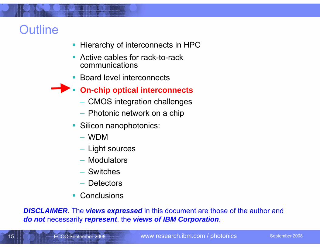
Wavelength multiplexers
70oC
25oCH. F. Hamann,et al, IEEE Journ. Solid-State Circuits, 42, 56 (2007).
non-IBM -processor @3.3 GHz, 1.4 Vdd Si thermooptic coefficientn/dT=2*10-4 K-1
±15°C
AWGMMI Lattice filters Ring resonator filtersEchelle grating
Number of channelsXtalkFootprintInsertion loss Temperature tolerancesFabrication tolerances
ECOC September 2008 September 200829 www.research.ibm.com / photonics
Wavelength multiplexers
Ultra-compact (200x200um2) Tolerant to on-chip “hot spots”
±15°C temperature variations Low-loss <2dB insertion loss FEOL CMOS integration Small cross-talk 20dB
F. Horst, F.Xia, W.Green, S.Assefa, Y.-H. Kim, L. Sekaric, Y. Vlasov
F.Xia et al OFC 2007F. Xia et al Optics Express 15, 17106 (2007).
F. Xia et al Opt. Express, 15, 11934 (2007)
F. Horst et al SPIE Europe March 2008

ECOC September 2008 September 200830 www.research.ibm.com / photonics
Cascaded Lattice filters
Phase error due to variations of the waveguide width of the order of just a few nm
3 cascaded MZI filters
F.Horst et al , SPIE Europe, Feb. 2008
400x300um
Cross-talk 15db (13dB with 2 outliers)
Insertion loss 1.5dB

ECOC September 2008 September 200831 www.research.ibm.com / photonics
Echelle grating
250x200um
Cross-talk 17db
Insertion loss 4dB
No active tuning. As-fabricated!
F.Horst et al , SPIE Europe, Feb. 2008
650x170um
Cross-talk 19db
Insertion loss 3dB
“safe”design
“extreme”design

ECOC September 2008 September 200832 www.research.ibm.com / photonics
2 nm wide error-free operating window @ 10 Gbps Temperature independent operation ±15°C
±150C
Y. Vlasov, W. M. J. Green, and F. Xia, Nature Photonics 2008
40x70um (6 channels, 400GHz)Cross-talk 30dbInsertion loss 1.3dB
F.Xia et al Optics Express (2007).
Ring resonator WDM filters

ECOC September 2008 September 200833 www.research.ibm.com / photonics
140346MEASURED
0.01220.0168RANGE
0.00900.00773SIGMA
0.19600.4843AVERAGE
GAPWIDTH
Wafer-to-wafer variation of all ringsDie-to-die variation of a single ring
2422MEASURED
0.0110.0065RANGE
0.00870.00533SIGMA
0.19860.4802AVERAGE
GAPWIDTH
1.2nm
16nm35nm40nm
Total tolerance3
EUV
193nm, OPC193nm, OPC248nm, OPC
Litho
22nm
45nm65nm
130nm
CMOS generationITRS CMOS tolerances for different technologies
Scaling of Si CMOS is done –performance will only increase with new generations of CMOS
Prospects for ultimate integrated CMOS photonics
193nm litho
2um

ECOC September 2008 September 200834 www.research.ibm.com / photonics
Outline Hierarchy of interconnects in HPC Active cables for rack-to-rack
communications Board level interconnects On-chip optical interconnects
– CMOS integration challenges– Photonic network on a chip
Silicon nanophotonics:– WDM– Light sources – Modulators– Switches– Detectors
Conclusions
DISCLAIMER. The views expressed in this document are those of the author and do not necessarily represent. the views of IBM Corporation.

ECOC September 2008 September 200835 www.research.ibm.com / photonics
Outline Hierarchy of interconnects in HPC Active cables for rack-to-rack
communications Board level interconnects On-chip optical interconnects
– CMOS integration challenges– Photonic network on a chip
Silicon nanophotonics:– WDM– Light sources – Modulators– Switches– Detectors
Conclusions
DISCLAIMER. The views expressed in this document are those of the author and do not necessarily represent. the views of IBM Corporation.

ECOC September 2008 September 200836 www.research.ibm.com / photonics
Modulator with external CW laser

ECOC September 2008 September 200837 www.research.ibm.com / photonics
Broadband MZI modulator Ultra-compact cross-section: ~0.1 m2
Simultaneous localization of injected free carriers and optical mode profile:1. Large change in carrier density during each ON-
OFF modulation cycle
2. Nearly complete carrier/optical mode overlap
Ultra-compact bend radius < 5 m– Device footprint limited only by length of phase
shifter
W. M. J. Green, et alOptics Express Dec. 2007
Vac
Vb

ECOC September 2008 September 200838 www.research.ibm.com / photonics
Fast operation
Broadband, non-resonant modulator High speed operation: 10 Gbps Ultra-compact footprint: ~ 0.001 mm2
10-100X smaller than previous MZIs Only 5x larger than microring modulator
5 Gbps: LMZM = 100 m

ECOC September 2008 September 200839 www.research.ibm.com / photonics
Low RF power
10 Gbps: LMZM = 200 m
Low RF power: 51 mW or 5 pJ/bit
DC power 287uWRF power 51mW

ECOC September 2008 September 200840 www.research.ibm.com / photonics
Outline Hierarchy of interconnects in HPC Active cables for rack-to-rack
communications Board level interconnects On-chip optical interconnects
– CMOS integration challenges– Photonic network on a chip
Silicon nanophotonics:– WDM– Light sources – Modulators– Switches– Detectors
Conclusions
DISCLAIMER. The views expressed in this document are those of the author and do not necessarily represent. the views of IBM Corporation.

ECOC September 2008 September 200841 www.research.ibm.com / photonics
Broadband Deflection Switch
Design Metrics: High throughput – 1Tbps
Low latency – few ns
Ultra-compact footprint < 0.001 mm2
Low crosstalk < -25 dB
High extinction ratio > 10 dB
Temperature independent operation ±15°C

ECOC September 2008 September 200842 www.research.ibm.com / photonics
Switching Characteristics
Free carrier injection into central ring: Drop port transmission suppressed by >15dB Through port transmission increases to zero loss
INPUT
DROP
THRU
Laserspot
Y. Vlasov, W. M. J. Green, and F. Xia, Nature Photonics 2, pg. 242-246 (2008).

ECOC September 2008 September 200843 www.research.ibm.com / photonics
Multi-Channel 40 Gbps Operation
Wavelength-insensitive operation Up to 360 Gbps throughput: 9 x 40 Gbps
~1 Tbps by reducing FSR
OFF - ThruON - Drop
OFF - Drop

ECOC September 2008 September 200844 www.research.ibm.com / photonics
Broadband High-Throughput 360 Gbps Switch
Error-free (BER > 10-12) operation @ 40 Gbps Power penalty < 0.3 dB in switch ON state
Cascaded switch fabric

ECOC September 2008 September 200845 www.research.ibm.com / photonics
Electrical injection
Photolithography
CMOS integration
Cascaded switch fabric

ECOC September 2008 September 200846 www.research.ibm.com / photonics
Outline Hierarchy of interconnects in HPC Active cables for rack-to-rack
communications Board level interconnects On-chip optical interconnects
– CMOS integration challenges– Photonic network on a chip
Silicon nanophotonics:– WDM– Light sources – Modulators– Switches– Detectors
Conclusions
DISCLAIMER. The views expressed in this document are those of the author and do not necessarily represent. the views of IBM Corporation.

ECOC September 2008 September 200847 www.research.ibm.com / photonics
Current Gen. CMOS +1 Gen. CMOS
CMOS scaling
Area 2X smallerPower per circuit 2.8X lower
Photonics scaling
Area 10-20XPower 30-100X
On-chip networksTele- and Data-com
Equivalent to 5-10 generations of CMOS
Challenges for on-chip nanophotonics
Best available integrated photonics(either InP or CMOS Si/Ge)
BW ~40-1000GbpsPower ~ 50pJ/bitArea ~0.5cm2

ECOC September 2008 September 200848 www.research.ibm.com / photonics
Summary
Opt
ical
I/O
Requirements from system level should define the requirements and performance metrics for individual devices
These requirements are very tough and almost impossible to meet
Nevertheless at the moment it looks that there is a room for innovation