Embed Size (px)
Citation preview

NOVEL 3-D ALL-POLYMER HIGH COLLECTION EFFICIENCY
PATHOGEN DETECTION BIOCHIP
_______________
A Thesis
Presented to the
Faculty of
San Diego State University
_______________
In Partial Fulfillment
of the Requirements for the Degree
Master of Science
in
Bioengineering
_______________
by
Vinothkumar Vijayaraghavan
Summer 2010


iii
Copyright © 2010
by
Vinothkumar Vijayaraghavan
All Rights Reserved

iv
DEDICATION
This thesis is dedicated to my parents, Vijayaraghavan and Shantha Devi, who have
raised me to be the person I am today.
Also I dedicate this thesis to my sister Vinodhini Vijayaraghavan and my fiancée,
Namratha Tata who have been a great source of motivation and inspiration.
I thank them for all the unconditional love, guidance, and support that they have
given me throughout my life.

v
“You must be the change you wish to see in the world” – Mahatma Gandhi.

vi
ABSTRACT OF THE THESIS
Novel 3-D All-Polymer High Collection Efficiency Pathogen Detection Biochip
by Vinothkumar Vijayaraghavan
Master of Science in Bioengineering San Diego State University, 2010
Biological imaging for isolation and concentration of pathogen or sub-micron particle
is an emerging field covering a wide range of applications critical to biological and clinical research. A variety of these applications often require isolation of rare cells or diluted pathogens from large volumes (few ml) of complex biological samples. Isolation of pathogens using active electrophoresis involving microarrays enables volume-level transport, accumulation, and hence separation of pathogens and cells. In conventional microarrays, the electric field away from planar electrodes decays rapidly, resulting in an inability to collect and isolate samples effectively. Hence for biological applications involving high-volume manipulation, microarrays with 3-dimensional electrodes provide an efficient solution. The use of 3-D microarrays with carbon electrodes for isolation of DNA offers wider range of manipulating voltage for large volume samples. To analyze the efficiency of accumulation in 3-D microarrays, electrophoretic experiments are carried out by manipulating the polystyrene beads (which mimic the DNA) in a high-efficiency, high-volume 3-D C-MEMS fabricated biochip using closed-cell electrophoresis. Experiments are captured with a CCD camera and 2-D image processing is carried out using Matlab. Individual Regions of Interest (ROI) were created on a biochip and examined using the multi-location capability of Matlab. This allowed the description of beads’ (i) dynamic distribution of beads, (ii) movement of beads from one electrode to another electrode when biased, (iii) accumulation (before and after biasing), and (iv) repulsion (before and after biasing). Algorithms were developed to measure the performance of a biochip for comparing the efficiencies of various ROIs in and around positively and negatively charged electrodes. Further 3-D Image Analysis is conducted for demonstrating the ability of the 3-D electrode to accumulate beads along its height (Z-axis) using Scanning Electron Microscopy and Hirox digital microscopy followed by the quantification of percentage accumulation using Keyence digital microscopy. The results of quantification suggest that in 3-D microarrays, the concentration of accumulation at the electrodes increases 10 folds from initial concentration. Further the analysis on 2-D metal vs. 3-D carbon electrodes establish that there is higher rate of accumulation with 3-D carbon electrodes and hence establishes a critical proof that 3-D carbon electrode microarrays could enable high collection efficiency biochips.

vii
TABLE OF CONTENTS
PAGE
ABSTRACT ......................................................................................................................... vi
LIST OF TABLES ............................................................................................................... ix
LIST OF FIGURES ............................................................................................................... x
LIST OF PAPERS ............................................................................................................. xiii
ACKNOWLEDGEMENTS ................................................................................................ xiv
CHAPTER
1 INTRODUCTION ..................................................................................................... 1
2 LITERATURE SURVEY .......................................................................................... 4
2.1 DNA Microarrays........................................................................................... 4
2.2 Pathogen Detection Systems ........................................................................... 6
2.3 Electrophoresis in Microarrays ....................................................................... 8
2.4 2-D vs. 3-D Electrodes ................................................................................. 10
2.5 Metal-Based and Polymer-Based Biochips ................................................... 14
2.6 Image Analysis ............................................................................................. 16
3 BIOCHIPS FOR PATHOGEN DETECTION .......................................................... 22
3.1 Electrophoresis ............................................................................................. 23
3.2 Microfluidics ................................................................................................ 28
4 FABRICATION OF C-MEMS MICROARRAY AND PACKAGING UNIT .......... 31
4.1 Fabrication of C-mems Microarray ............................................................... 31
4.2 Packaging Unit ............................................................................................. 35
5 ELECTROPHORETIC EXPERIMENTATION ....................................................... 40
6 IMAGE PROCESSING AND 3-D ANALYSIS ....................................................... 52
6.1 Image Processing Using Software ................................................................ 52
6.2 Three Dimensional Analysis ......................................................................... 60
6.2.1. Live 3-D Experimentation: Hirox Digital Microscope ......................... 61
6.2.2. 3-D Analysis Using Scanning Electron Microscope (SEM) ................. 62
6.2.3. 3-D Analysis Using Keyence Digital Microscope ............................... 68

viii
6.2.3.1 Profiling Across The Trace ......................................................... 70
6.2.3.2 Profiling Across Electrodes ......................................................... 71
6.2.3.3 Profiling 3-D Electrode ............................................................... 72
6.3. Quantifying Beads Along The Walls of 3-D Electrode ................................ 73
6.3.1 Calculation for Beads Stacks along the Walls of the 3-D Electrode ...................................................................................................... 74
6.4. Calculation of Beads on 2-D Electrode ........................................................ 76
6.5. Calculation of Beads on 3-D Electrode ........................................................ 77
6.6 Comparison of 2-D and 3-D Electrodes ........................................................ 79
7 FINITE ELEMENT ANALYSIS ............................................................................. 80
8 RESULTS AND DISCUSSIONS ............................................................................ 85
8.1 Concentration of Accumulation Based on Image Processing Techniques ......................................................................................................... 85
8.2 Concentration of Accumulation Using Image Analysis Techniques .............. 87
8.3 Comparison of 2-D vs. 3-D Electrodes ......................................................... 90
9 CONCLUSION ....................................................................................................... 92
REFERENCES.................................................................................................................... 94
APPENDIX
IMAGE PROCESSING: MATLAB CODES ............................................................... 102

ix
LIST OF TABLES
PAGE
Table 2.1. Summary of Literature Survey .............................. Error! Bookmark not defined. Table 4.1. Multi-step Heating Schedule for Pyrolysis .......................................................... 34
Table 4.2. Heat Cure Specifications for Baking PDMS ........................................................ 38
Table 6.1. Mencoder Commands and Description ................................................................ 54
Table 6.2. Accumulation Concentration of Beads With Respect to Frames .......................... 57
Table 6.3. Concentration of Accumulated Beads ................................................................. 58
Table 6.4. Increased Accumulation Concentration of Beads with Respect to Time .............. 58
Table 6.5. Increased Concentration of Accumulated Beads .................................................. 59
Table 6.6. Depletion Concentration of Beads With Respect to Frames ................................. 59
Table 6.7. Decreased Concentration of Accumulated Beads ................................................ 60
Table 8.1. Comparison of DNA Accumulation on 2-D Electrodes ....................................... 86
Table 8.2. Concentration of Beads: 2-D vs. 3-D ................................................................... 90

x
LIST OF FIGURES
PAGE
Figure 1.1. Electronically active microarray researches in MEMS lab, SDSU. ....................... 3
Figure 2.1. Electric field medicated DNA micro-array.. ......................................................... 5
Figure 2.2. Areas of interest for pathogen detection and reported detection with Salmonella and E.Coli. .............................................................................................. 8
Figure 2.3. Accumulation of DNA at anode with respect to time. .......................................... 9
Figure 2.4. Computed iso-electric field distributions.. .......................................................... 11
Figure 2.5. 2-D and 3-D comb electrodes: (a) Flat 2-D and (b) 3-D….................................. 12
Figure 2.6. Cyclic voltammograms of the 3-D electrode and 2-D planar electrode ............... 13
Figure 2.7. Trapping efficiencies ......................................................................................... 13
Figure 2.8. View of 3-D silicon electrode.. .......................................................................... 15
Figure 2.9. Alexa-Fluor 430 labeled streptavidin ................................................................. 17
Figure 3.1. Schematic diagram of the multi-functional biochip ............................................ 23
Figure 3.2. Schematic diagram of electrical double-layer ..................................................... 24
Figure 3.3. Agarose gel electrophoresis method ................................................................... 27
Figure 3.4. Schematic diagram of capillary electrophoresis .................................................. 28
Figure 3.5. Showing the sketch of measured physical quantity ............................................. 29
Figure 3.6. A microfluidics device for selective capturing of target cells ............................. 30
Figure 4.1. Schematic diagram of CMEMS process ............................................................. 32
Figure 4.2. Silicon wafer spin-coating. (a) dispersing photoresist on wafer and (b) wafer with SU-8 10 thickness of 10µm. ................................................................... 33
Figure 4.3. Wafer spin-coated with SU-8 100 with a thickness of 220µm. ........................... 34
Figure 4.4. SEM Pictures of microarray. (a) 3x3 (b) 5x5 (c) 10x10. ..................................... 35
Figure 4.5. Bottom case: (a) top view and (b) isometric view. .............................................. 36
Figure 4.6. Top case: (a) top view and (b) isometric view. ................................................... 37
Figure 4.7. PDMS mold case. (a) top view and (b) isometric view. ...................................... 38
Figure 4.8. Carbon microarray biochip packaging unit. ........................................................ 39
Figure 5.1. Electrophoretic experimental setup. ................................................................... 40
Figure 5.2. Sketch of carbon microarrays. (a) 3×3, (b) 5×5, and (c) 10×10. ......................... 41

xi
Figure 5.3. 10×10 microarray chip. ...................................................................................... 42
Figure 5.4. Biasing of bump pads through top case. ............................................................. 43
Figure 5.5. Electrophoretic experimentation: Accumulation. (a), (b), (c), and (d) Showing accumulation of negatively biased beads towards anode region with respect to time ......................................................................................................... 44
Figure 5.6. Peeling of electrodes. ......................................................................................... 47
Figure 5.7. Electrophoretic experimentation: Repulsion. (a), (b), (c), and (d) Showing depletion of negatively biased beads from cathode region with respect to time. ........ 48
Figure 5.8. Summary of electrophoretic experimentation. .................................................... 51
Figure 6.1. Zarbeco video toolbox pro. ................................................................................ 53
Figure 6.2. Region of Interest (ROI). ................................................................................... 54
Figure 6.3. Color codes. ...................................................................................................... 55
Figure 6.4. Image processing of chip showing equal concentration of beads at ROI 1 and ROI 2. ............................................................................................................... 56
Figure 6.5. 10×10 microarray. (a) and (b) Image processing of accumulation at ROI 1 and depletion of beads at ROI 2. .............................................................................. 56
Figure 6.6. Accumulation of beads concentration vs. frame numbers. .................................. 57
Figure 6.7. Increased accumulation of beads vs. frame numbers. ......................................... 59
Figure 6.8. Depletion of beads concentration vs. frame numbers. ......................................... 60
Figure 6.9. Hirox digital microscope.................................................................................... 61
Figure 6.10. 3-D electrophoretic experiment. (a) accumulation and (b) repulsion. ................ 62
Figure 6.11. SEM image showing the accumulated beads around the 3-D electrodes. .......... 63
Figure 6.12. SEM image of accumulated beads on trace between two electrodes. ................ 63
Figure 6.13. Closer view of the beads on trace between two electrodes. ............................... 64
Figure 6.14. Image of individual beads under SEM. ............................................................ 65
Figure 6.15. SEM image showing the stacking of beads along the walls of the electrode. ................................................................................................................. 65
Figure 6.16. SEM image showing the accumulation at anode. (a) front view (b) rear view (c) left view and (d) right view. ....................................................................... 66
Figure 6.17. SEM image of 3-D electrodes. (a) negatively biased electrode without beads and (b) positively biased electrode with beads. ............................................... 66
Figure 6.18. SEM image showing top view of the electrode. (a) without beads, and (b) with beads. ............................................................................................................... 67
Figure 6.19. Types of accumulation of beads. ...................................................................... 68
Figure 6.20. Keyence digital microscope ............................................................................. 69

xii
Figure 6.21. Profiling of the accumulated chip. .................................................................... 69
Figure 6.22. Profiling across the trace. ................................................................................. 70
Figure 6.23. Profiling around the electrode. ......................................................................... 72
Figure 6.24. Profiling 3-D electrode. ................................................................................... 73
Figure 6.25. Schematic representation of beads at the base of the electrode. ........................ 74
Figure 6.26. Beads accumulated at the base of the electrode represented as a triangle ABC. ....................................................................................................................... 75
Figure 6.27. Schematic representation of 2-D electrodes. ..................................................... 76
Figure 6.28. Schematic representation of 3-D electrodes. ..................................................... 77
Figure 7.1. Schematic representation of 10×10 microarray. ................................................. 80
Figure 7.2. Electric field distribution in 2-D electronically active 10×10 microarray. ........... 81
Figure 7.3. Electric field distribution across section A-A. .................................................... 82
Figure 7.4. Electric potential distribution in 2-D electronically active 10×10 microarray. .............................................................................................................. 82
Figure 7.5. Electric potential distribution across section B-B. .............................................. 83
Figure 7.6. Accumulation concentration at anode. ............................................................... 83
Figure 7.7. Comparison of FEA and experimental results on concentration beads at anode. ...................................................................................................................... 84
Figure 8.1. Active DNA chip: 25-site chip ........................................................................... 85
Figure 8.2. Comparison of 2-D metal vs. 3-D carbon electrode using image processing techniques. ............................................................................................. 86
Figure 8.4. Workable window of 2-D metal vs. 3-D carbon electrode .................................. 91

xiii
LIST OF PAPERS
This thesis is based on the following presentations:
I. Namratha Tata and Vinothkumar Vijayaraghavan, “Image Processing of Novel All
Polymer High Collection Efficiency Bio-chip using MATLAB for Pathogen Detection”,
Student Research Symposium, SDSU (2009). [Dean’s award]
II. Namratha Tata and Vinothkumar Vijayaraghavan, “Novel 3-D All-Polymer High
Collection Efficiency Pathogen Detection Biochip”, Student Research Symposium, SDSU
(2010).

xiv
ACKNOWLEDGEMENTS
I would like to thank my thesis advisor, Dr. Sam Kassegne, who has helped me
throughout my research work. Thanks for helping me choose this thesis which implements
bio-instrumentation techniques as I always had a keen interest towards it and making my
dream come true.
I would also like to thank Dr. Sunil Kumar and Isai Michel from Department of
Electrical Engineering, Anson Hsu from Mechanical Engineering for helping me with Image
Processing and Dr. Steven Barlow from Biology Department for his assistance in Image
Analysis.
In addition, I would like to thank my fellow colleagues from MEMS Lab for their
valuable inputs towards my research. And last but not least, I would like to thank Dr. Karen
May-Newman and Dr. Robert Nelson for their patience during this research work.

1
CHAPTER 1
INTRODUCTION
Many advanced technologies in this rapidly evolving world are moving towards
miniaturization of products. In earlier days, giant computers which occupied a huge room
were considered a novelty compared to today’s trends in technology of products that has
introduced us to the luxury of laptops, net books, smart phones, etc. In 1959, a famous
physicist Richard Feymann gave a lecture at American Physical Society emphasizing the
concept of unexplored realm where he famously suggested that “there is plenty of room at
the bottom” [1]. This famous speech inspired scientists to think and manipulate matter on an
atomic scale. This thought gradually resulted in the development of a new technology called
MEMS (Micro Electro Mechanical Systems).
MEMS (also called as micro machines in Japan and Micro System Technology
(MST) in Europe) is a technology which integrates mechanical elements, actuators, sensors
and electronics on a common silicon substrate using microfabrication technology [2].
MEMS find applications in inertial systems, optical systems, bio-MEMS, RF devices, and
power and reactor Microsystems [3]. While traditionally silicon has been the material of
choice in MEMS, carbon, the fourth most abundant naturally occurring element on earth is
gaining popularity for use in MEMS and finds its application in biomedicine, solar cells, fuel
cells, micro batteries, etc. MEMS based on carbon pre-cursor material are called C-MEMS
(carbon-MEMS) [4].
Carbon based MEMS technology (C-MEMS) can be extended for developing
microarrays used in DNA, protein, cellular, tissue, and chemical compound microarray [5].
These microarrays work on the principle of isolation and concentration of rare cells,
pathogens, biomolecules and any sub-micron particles using embedded micro electrodes and
these are critical to any biological and medical application. Two-dimensional (2-D) planar
manipulation of such entities has been achieved in DNA microarray chips using
electrokinetic mechanisms such as electrophoresis (movement of charged particles/species

2
such as DNA in the presence of electric field) and dielectrophoresis ( movement of
polarizable particles in the presence of non-uniform electric field ) [6-9].
The major drawbacks with these separation and manipulation techniques are the
inability and inefficiency of processing large volume samples. This led to the fabrication of
microarrays with 3-dimensional (3-D) electrodes which are said to possess greater
efficiencies. Researchers like Kassegne et al. [10], Lu et al. [11], Honda et al. [12], and Tay
et al. [13] have demonstrated through simulations and electrochemical analysis that three
dimensional (3D) electrodes posses better trapping efficiency than two dimensional planar
electrodes. However there has been no significant publication showing the manipulation of
particles on a real time basis.
This thesis will target C-MEMS/Carbon-MEMS biochips used for pathogen detection
systems. These biochips have been fabricated on a silicon substrate with structures made by
pyrolyzing a polymer (negative photoresist) called SU-8, forming 3-D carbon microarrays.
The detection system in such microarrays is based on hybridization of species using
electrophoresis: the migration of particles to a specified region of interest in the flow cell in
the presence of electric field [14]. This technique is superior to other existing manipulation
mechanisms in terms of ease of use, detection efficiency and time. In this research
DNA/RNA is mimicked using polycarboxylate beads (1.94µm) that are negatively charged in
a 50mM histidine buffer solution. These experiments are conducted under closed cell
condition which uses a packaging unit made of polymer material with a
Polydimethylsiloxane (PDMS) seal.
In broader terms, the research plan on microarrays at SDSU is summarized in
Figure 1.1. As shown in Figure 1.1, the objective of this research is to demonstrate high
collection efficiency of 3-D Carbon biochips fabricated using CMEMS technology by
manipulating negatively charged beads using active electrophoresis. MATLAB has been
used for 2-D image processing of beads accumulating at the anode (positively charged
electrode) and their gradual depletion at cathode (negatively charged electrode). 3-D stacking
of beads in the z-axis i.e., along the walls of the electrode is proved using a live
electrophoretic experimentation using a Hirox digital microscope. Scanning Electron
Microscopy was used for imaging the accumulated beads followed by its stacking of beads
on one another. A 3-D profile was developed using a Keyence digital microscope profiler to

3
Figure 1.1. Electronically active microarray researches in MEMS lab, SDSU.
calculate the concentration of beads at (1) across the trace, (2) across the electrode, and
(3) on the electrode. Percentage of accumulation for 2-D and 3-D electrodes are calculated
and compared. Further finite element models are created for analyzing the electric field
distribution, electric potential distribution, and accumulation concentration of beads around
the anode using electrokinetic model.
This thesis is organized as follows: Chapter 1 gives a brief introduction about this
thesis; Chapter 2 reviews the literature survey on DNA microarrays, pathogen detection
systems, electrophoresis, 3-D vs. 2-D electrodes, metal based and polymer based biochip and
image Analysis; Chapter 3 examine biochips for pathogen detection; Chapter 4 explains the
C-MEMS microarray fabrication and its packaging unit; Chapter 5 puts forth the experiments
carried out using electrophoresis; Chapter 6 describes the 2-D and 3-D image analysis;
Chapter 7 covers the finite element modeling and analysis; Chapter 8 compares the obtained
results with the published journals; and Chapter 9 gives the final conclusions of this research.

4
CHAPTER 2
LITERATURE SURVEY
In this chapter, we will review in detail prior innovative ideas and models of
microarrays put forth by different researchers that served as guidance for this research. Our
motivation towards Bio-MEMS has always geared us to make a detailed analysis of pathogen
detection systems. In this chapter, we review microarrays, carbon & metal-based microchips
and their image analysis.
2.1 DNA MICROARRAYS Microarrays are generally non-destructive to the solution and species under
investigation and this advantage is significant in biological samples and for in-vivo
measurements where such destruction is not desired [15]. DNA microarray technology is
considered to be the successful merger between microelectronics technologies, biology and
chemistry. Even though microarrays have various applications, gene expression is being used
as a common technique. Wilson et al. developed a multi pathogen identification system
which could detect up to 8 different pathogens [16]. High capacity microarrays enables the
detection of 20,000 to 40,000 genes in a single experiment, thus enabling researches to attain
a complete picture of gene function using DNA microarray chips [17]. The DNA microarray
chip, also known as genome chip, is made up of electrode arrays with each electrode
immobilizing a known sequence of single stranded DNA (capture probes) that hybridizes
with an unknown sequence (target probes). The presence of a pathogen is detected when the
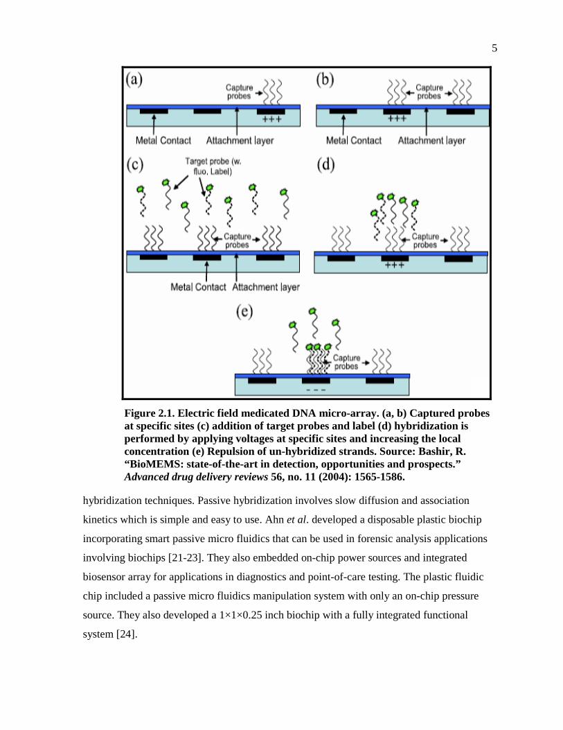
complementary base pair attaches with tagged target probes as shown in Figure 2.1[18].
DNA hybridization is a molecular biology technique that is used to determine the
genetic distance between two species [19]. Hybridization is based on the formation of a
stable double helix in which two complementary single stranded nucleic acid chains are
involved. These reactions can occur in two possible ways: (i) between a molecule in solution
and a complementary molecule immobilized on a solid post (probe) or (ii) between two
complementary molecules in solution [20]. They are classified in to passive and active
5
Figure 2.1. Electric field medicated DNA micro-array. (a, b) Captured probes at specific sites (c) addition of target probes and label (d) hybridization is performed by applying voltages at specific sites and increasing the local concentration (e) Repulsion of un-hybridized strands. Source: Bashir, R. “BioMEMS: state-of-the-art in detection, opportunities and prospects.” Advanced drug delivery reviews 56, no. 11 (2004): 1565-1586.
hybridization techniques. Passive hybridization involves slow diffusion and association
kinetics which is simple and easy to use. Ahn et al. developed a disposable plastic biochip
incorporating smart passive micro fluidics that can be used in forensic analysis applications
involving biochips [21-23]. They also embedded on-chip power sources and integrated
biosensor array for applications in diagnostics and point-of-care testing. The plastic fluidic
chip included a passive micro fluidics manipulation system with only an on-chip pressure
source. They also developed a 1×1×0.25 inch biochip with a fully integrated functional
system [24].

6
Affymetrix Inc. developed a microarray called GeneChip® for analyzing gene
sequences using passive hybridization. Their microarray was made using a oligonucleotide
fixed to the surface of the chip using photolithography and combinatorial chemistry. They
synthesized cDNA from RNA in order to hybridize the microarray. The hybridization took
16 long hours followed by sample wash [17]. Even though the passive methods of
hybridization are in use for pathogen detection they still lag behind because of their long
incubation time involved for efficient hybridization. However, on the other hand active
hybridization (i) utilizes rapid transport and selective addressing of DNA probes (ii) speeds
up of basic hybridization process and (iii) ensures that single base mismatches in target DNA
sequences are clearly discriminated [10].
Kassegne et al. developed a sensitive and highly accurate electro-optical DNA
microarray sensor with active hybridization technique capable of detecting more than one
analyte [10]. They monitored the assay using a scanning confocal optical platform for
fluorescence detection. They also designed a model showing the electric field distribution at
the biochip electrode array and electrokinetic [25-28] transport of DNA species under the
influence of electric field (i.e., the rate of transportation of DNA species to the anode) and
compared DNA accumulation through modeling and experimentation.
Huang et al. designed an active DNA hybridization chip with 25 – 10,000 µ
electrodes. It enabled electrophoretic transportation of charged molecules such as DNA,
RNA, antibodies and even micro beads. Each electrode could be addressed on an individual
basis for applying voltage and current [29].
2.2 PATHOGEN DETECTION SYSTEMS Novel approaches for pathogen detection has enabled DNA sequencing of entire
microbial genome and identification of certain microbial pathogen would help in developing
new treatment and disease prevention strategies [30]. In 1983, Mullis et al., developed
polymerase chain reaction (PCR) technique, a DNA based diagnostic method to overcome
the difficulties in culturing and contamination encountered in conventional pathogen
detection systems [31]. As PCR is based on amplifying and making copies of specific target
DNA, it has been difficult to accurately quantify the number of accumulated copies [32].
Applied Biosystems, Inc introduced an instrument which used fluorescently labeled species-

7
specific DNA sequence (probe) in to the PCR amplification system to quantify the amplified
copies of DNA [33]. This new process called Quantitative PCR (QPCR) amplifies and
detects pathogen within 30 minutes whereas the conventional PCR techniques would take 2
to 6 hours [34]. Even though QPCR is advantageous over PCR, it encounters difficulties
when it comes to complex biological detection [35].
Technological development in DNA sequencing continues to improve day by day. A
prominent genetics institute recently sequenced its trillionth base pair of DNA, proving the
rapid development of DNA sequencing of this century [36]. This is in comparison to the
Moore’s law which exhibits the fast growing trends in micro technology [37]. But why do we
want to talk about DNA sequencing in pathogen detection? This is because each species of
pathogens carries with it a unique DNA or RNA that differs from other organisms [38]. So
by sequencing the DNA/RNA of a particular pathogen we can determine its characteristics
and effects on organisms.
Oliver et al. aims to give an overview of the pathogen detection in the field of food
industry, where failure to detect an infection may cause terrible consequences. They focus
only on analytical dimension: detection, identification and quantification, with an emphasis
on pathogen biosensors with rapid detection methods [39, 40] which cut down on the time
factor involved in the standard bacterial detection that typically takes up to 7 or 8 days to
yield results. Pathogen detection is of utmost importance, primarily for the health and point
of care sectors most of which involves detection of Salmonella and E-Coli as shown in
Figure 2.2 [41].
Many pathogen detection methods are being used in biomedical applications [42]
based on mechanical, electrical and optical detection modalities. Bashir (2004) reviews
various detection techniques used in BioMEMS and Biochip sensors. The mechanical
detection involves using cantilever sensors on a chip, where it can perform stress sensing and
mass sensing. The electrical method is based on (i) amperometric biosensors that involve the
electric current associated with the electrons involved in the redox process (ii) potentiometric
biosensors involve change in potential at electrodes due to ions or chemical reactions that
occur (iii) conductometric biosensors involve measuring conductance changes associated
with changes in the overall ionic medium between the two electrodes [18]. In optical
detection technique, DNA, proteins and other molecules are identified using fluorescence

8
Figure 2.2. Areas of interest for pathogen detection and reported detection with Salmonella and E.Coli. Source: Javier, C., L. Oliver, and M. Xavier. “Pathogen detection: A perspective of traditional methods and biosensors.” Biosensor and Bioelectronics 22, no. 7 (2007): 1205-1217.
which is tagged to the target probes and quantified using laser detection. The capture probes
are coated with an antibody that will later bind to the target probes. However the common
drawback of this system is lack of specificity [43].
2.3 ELECTROPHORESIS IN MICROARRAYS Historically, DNA separation and manipulation was considered to be laborious and
time consuming task and was based on gravity separation methods. During 1970’s a
separation technique called Gel Electrophoresis was introduced. This technique involved
separation of DNA fragments using electric field in porous sponge-like matrix where smaller
molecules pass through the matrix faster than other larger molecules [44]. A Gel
Electrophoresis cell is typically an electrochemical cell which consists of an anode, a
cathode, a gel electrolyte and charged particles [45]. Usually the charged particle is DNA of

9
pathogens like bacteria, viruses, fungi etc. But there are certain disadvantages using gel
electrophoresis separation technique: The gels that are used in electrophoretic experiment can
melt down or the buffer could get exhausted. Further various kinds of genetic material may
run in unpredictable forms and not be suitable for high throughput analysis [46, 47]. In order
to overcome these drawbacks, a technique known as Capillary Electrophoresis was
introduced in early 1980’s and is still being used in the fields of analytical chemistry,
biotechnology, biomedical and pharmaceutical sciences [48].
Kassegne et al. investigated the transport and accumulation of biomolecules,
particularly DNA, through numerical modeling and experimental verification on
electronically active biochips. Simulation results for the accumulation of DNA at the surface
of the anode vs. time are comparable with the experimental results as in Figure 2.3 [49].
Figure 2.3. Accumulation of DNA at anode with respect to time. Source: Kassegne, S., A. Hodko, M. Madou, K. Sarkar and J. Yang. “Numerical modeling of transport and accumulation of DNA on electronically active biochips.” Sensors and Actuators B: Chemical 94, no. 3 (2003): 81-98.
Tagliaroa et al. presented a paper on introduction to Capillary Electrophoresis (CE)
that explains its basic concepts and mechanisms [50]. He also gave an overview into the new
technologies and applications of CE. Such CE experimental setup consists of an injection
system, a separation capillary (20-100µm I.D., 20-100 cm length), a high voltage source
(30KV) and current source (200-250µA). In his paper, he explains two types of CE

10
techniques: hydrodynamic and electro kinetic. The former uses pressure or vacuum, while the
later operates by application of potential [51].
One of such capillary technique developed by Adachi et al. for microbial analysis of
bacteria 16S rRNAs was based on affinity capillary electrophoresis [52] using 16S rRNA-
conjugated magnetic beads which is a very powerful analytical method for gene analysis and
mutation assay [53-56]. In their experiment, RNA conjugated magnetic beads were
introduced into the capillary from cathodic ends by positive pressure and was localized in the
middle using a magnet. Tris-borate buffer containing MgCl2 was then introduced into the
capillary followed by the fluorescently labeled probe for hybridization. When a high electric
field is applied, the DNA probes migrated electrophoretically towards the anode. During the
migration of DNA, the fluorescently labeled probe hybridized to the target 16S rRNA on the
magnetic beads. The excess beads that were not hybridized were washed away from the
capillary cell [57].
LeBlanc et al. reports a novel method for the detection of four pestivirus: Classical
swine fever virus (CSFV), Border disease virus (BDV), Bovine viral diarrhea virus type 1
(BVDV1) and type 2 (BVDV2). The process utilizes an oligonucleotide microarray by means
of supraparamagnetic streptavidin-coupled magnetic beads detection. In their experiment,
magnetic beads are added to the array and a planar solid magnet is placed below the array
slide [58]. This facilitates the magnetic migration of beads to the array surface and the
interaction of beads with the probes. After 30s, the direction of the magnetic field was
reversed by placing the magnet above the microarray for 10s to remove unbound and weakly
bound beads. The liquid in the array was removed followed by the bead detection using a
light microscope and Image analysis software was used to analyze the final images [59, 60].
It is evident that when the electric field is highly positive, there is huge accumulation of
beads and vice versa.
2.4 2-D VS. 3-D ELECTRODES Cheng et al. developed an array based CMOS biochip for DNA detection using self-
assembled multilayer gold nanoparticles (AuNPs) [61]. Experimentation was conducted for
DNA hybridization using the array based CMOS biochip with both monolayer and multilayer
AuNPs. Their cyclic voltammetry results indicate that the electrical current density at the
11
gold nanoparticle multilayer exceeded that of gold nanoparticle monolayer by three orders of
magnitude [62].
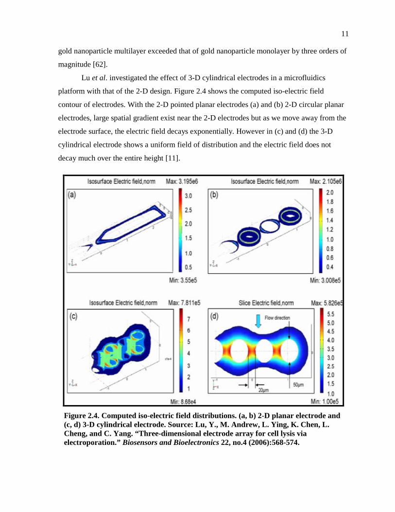
Lu et al. investigated the effect of 3-D cylindrical electrodes in a microfluidics
platform with that of the 2-D design. Figure 2.4 shows the computed iso-electric field
contour of electrodes. With the 2-D pointed planar electrodes (a) and (b) 2-D circular planar
electrodes, large spatial gradient exist near the 2-D electrodes but as we move away from the
electrode surface, the electric field decays exponentially. However in (c) and (d) the 3-D
cylindrical electrode shows a uniform field of distribution and the electric field does not
decay much over the entire height [11].
Figure 2.4. Computed iso-electric field distributions. (a, b) 2-D planar electrode and (c, d) 3-D cylindrical electrode. Source: Lu, Y., M. Andrew, L. Ying, K. Chen, L. Cheng, and C. Yang. “Three-dimensional electrode array for cell lysis via electroporation.” Biosensors and Bioelectronics 22, no.4 (2006):568-574.

12
Honda et al. fabricated 3-D electrodes for electrochemical detection that are highly
applicable to immunoassays. The dimensions of their electrode were 10µm and 30µm in
width and height respectively with 20µm spacing in between. Figure 2.5 shows that the redox
species near the 3-D electrode surface have much improved trapping ratio (97.9%) along the
z-axis compared to that of the 2-D planar electrode trapping ratio (62%), thus the 3-D comb
electrode system will lead to an improved electrochemical detection system [12]. As shown
in Figure 2.6, the cyclic voltammograms reveals that the output current of the 3-D electrodes
was eight times larger when compared to the 2-D planar electrodes.
Figure 2.5. 2-D and 3-D comb electrodes: (a) Flat 2-D and (b) 3-D. Source: Honda, N., M. Inaba, T. Katagiri, S. Shuichi, S. Hirotaka, H. Takayuki, O. Tetsuya, S. Mikiko, J. Mizuno, and W. Yasuo. “High efficiency electrochemical immuno sensors using 3D comb electrodes.” Biosensors and Bioelectronics 20, no. 11 (2005): 2306-2309.
Electrical and thermal characterization of 3-D biochip was described by Tay et al.
Their research work included comparing the trapping efficiency of 2-D planar electrodes and
3-D silicon electrodes. Figure 2.7 shows that the trapping efficiency of 2-D planar electrode
is very low when compared to 3-D trapping efficiency. It is evident from their numerical
simulation using finite element method (ANSYS), that the changes in temperature at the 3-D
silicon electrodes were 8 times -10 times lower than that of the 2-D planar electrodes [13].

13
Figure 2.6. Cyclic voltammograms of the 3-D electrode and 2-D planar electrode. Source: Honda, N., M. Inaba, T. Katagiri, S. Shuichi, S. Hirotaka, H. Takayuki, O. Tetsuya, S. Mikiko, J. Mizuno, and W. Yasuo. “High efficiency electrochemical immuno sensors using 3D comb electrodes.” Biosensors and Bioelectronics 20, no. 11 (2005): 2306-2309.
Figure 2.7. Trapping efficiencies: (a) 2-D planar electrode, and (b) 3-D silicon electrode. Source: Tay, F., Y. Liming, J. Pang, and I. Ciprian. “Electrical and thermal characterization of a dielectrophoretic chip with 3D electrodes for cells manipulation.” Electrochemical Actuators 52, no. 8 (2007): 2862-2868.
All the researches based on 2-D planar electrodes and 3-D electrodes have confirmed
that, when comparing 2-D electrode with the 3-D electrodes, have the following advantages:
(1) High electrical current density, (2) Good trapping efficiency, and (3) Uniform electrical
and thermal distributions.

14
2.5 METAL-BASED AND POLYMER-BASED BIOCHIPS Microarray biochip technology has become a very important field for investigation by
both industrial and academic research groups. Biochips were developed in a micro arrayed
fashion for pathogen detection using both metal based and polymer based materials.
Cui et al. represented a microelectrode 5×5 array integrated biochip for detecting
Dopamine (DA) – an important neurotransmitter playing a vital role in many neurological
disorders [63]. The biochip is silicon based and the 5×5 array is made of gold disk
microelectrodes. MN9D, a mouse mesencephalic dopaminergic cell had been placed on the
sterilized silicon dioxide surface of the biochip chamber and incubated in DMEM
(Dulbecco’s Modified Eagle’s Medium) for 48h. These MN9D cells attached (80-90%) on
the Au disc (60µm) 5×5 planar disc microelectrode array was then observed under a
microscope. Also, Cyclic Voltametry indicates that a current of 20nA could be attained for a
voltage of 0.5V [64].
Chu et al. developed a 10×10 3-dimensional micro electrode array with 100µm
spacing between the microelectrodes. This microarray device has been used in biomedical
application for bio-neural recordings. Figure 2.8 shows the 3-D electrodes fabricated via a
three-mask process for integrating the signal lines with electrodes and bond pads with 60µm
height and 30µm diameter [65]. However microarrays made of metal and silicon posses
certain drawbacks. As fabricating 3-D microarrays with such materials would not be an
economical option and also due to the fact that metals operate in narrower electrochemical
window, other material options have to be considered. On the other hand, polymers are
cheaper than silicon and metals and they are more flexible and bond more easily to other
materials than silicon and glass [66].
Johnson et al. addressed a simple glass-polymer based biosensor for the detection of
beads where different bead types were incorporated and identified based on their spatial
addresses without the need for color coding [67, 68]. They introduced distinct bead types
conjugated with different oligonucleotide probes that are sequentially spotted on to a gel pad
on the surface of the device [69].
Marquette and Blum developed and validated a new electro-chemiluminescent
biochip in 2004. Silicon based organic polymer material, Polydimethyl siloxane (PDMS) and
graphite elastomer was used to build the biochip. Their research shows the technical

15
Figure 2.8. View of 3-D silicon electrode. Source: Baowen, C., C. Chuan, H. Chu, S. Lu, K. Tzu, and F. Weileun. “Design and fabrication of novel three-dimensional multi-electrode array using SOI wafer.” Sensors and Actuators A: Physica 130, no. 1 (2006): 254-261.
difficulties encountered in producing an array with individually wired active electrodes and
propose a method to solve this problem by introducing an elastomer/graphite organized solid
where the micro beads (Sepharose beads) could be physically entrapped. It is found that the
electrochemical window of PDMS and a graphite elastomer using Cyclic Voltametry is
between -0.5V to 0.5V [70].
Although polymers like PDMS have good bonding properties and are cheaper when
compared to silicon, there are certain drawbacks using them as structural MEMS material.
Gravity, adhesion and capillary forces stress the structures made of PDMS and consequently
leads in collapsed features [66]. Due to these disadvantages, it is not recommended to build
3-dimensional electrode structures using PDMS. In order to reduce the cost incurred in
manufacturing as well as the need to develop efficient systems for use in pathogen detection
systems, researches came up with a new fabrication technology called the C-MEMS (carbon
MEMS ) technology. The carbon based material used in this technology enables MEMS
device to meet both technological and economical needs. Graphite, diamond, glassy carbon,
amorphous carbon etc. [71] has been widely used in various fields due to its biocompatibility.
Carbon based MEMS (C-MEMS) technology involves pre-patterning organic
structures made of photo patternable polymers and treating them in inert or reducing
atmospheres at a high temperature. This process is known as pyrolysis and is carried out in a

16
vacuum or a forming gas furnace at temperature above 1000ºC [72, 73]. Typical materials
used include Su-8 a negative photoresist and AZ-4620 a positive photoresist which are easily
patternable using photolithographic techniques to fabricate 3-D structures. These materials
when pyrolyzed are converted into conductive carbon and posses (1) stable microarray
structures (2) bio-compatible properties (3) wide electrochemical window (4) easy
manufacturability and (5) economical mass production capabilities.
2.6 IMAGE ANALYSIS Meaningful information obtained from digital images by means of digital image
processing techniques is known as Image analysis [74]. These digital images can be captured
using a CCD camera followed by analysis using computers. Various sections of the obtained
images are analyzed by selecting a region i.e., Region of Interest (ROI).
Mehta et al. developed and characterized a multipoint parallel excitation and CCD
based imaging for fluorescence detection of a 19×19 microarray of 2-dimensional biochip.
High-throughput parallel detection and quantitative analysis of the fluorescent was obtained
by CCD based imaging system. The performance of the system was obtained using a
microarray sample of cyanine (Cy5) dye dots on silicon wafer and on glass substrate with
varying concentrations. These cyanine dyes are subjected to imaging where the CCD camera
is used to calculate the pixel number of each fluorescence microarray element [75].
Kurzbuch et al. presented a fluorescence chip reader for easy, multiplexed assay
measurement on plastic biochips. The system is designed as a low cost, compact and robust
instrument for point-of-care testing. A custom designed piezo-motor-driven scanning stage is
coupled to an optical element. Supercritical angle fluorescence (SAF) is used for
fluorescence imaging of biochip array. These SAF techniques not only enhance the
fluorescence collection efficiency but also confine the fluorescence detection volume strictly
to the close proximity of the biochip surface, thereby discriminating against fluorescence
background from the analyte solution. The polymer biochip used here is with dimensions of
75mm×25mm× 1.2mm and the fluorescence beads are of 200nm dark red from Invitrogen.
The combination of high collection efficiency and the surface selectivity of the SAF
detection technique yield a generic Limit of Detection (LOD) of 0.14 Cy5 fluorophores per
square micrometer [76]. Cooper et al. developed a convenient biochip, feasible for imaging

17
technology, measuring fluorescence intensity of protein spot arrays. These proteins are
arrayed on to a membrane using a new method that combines the use of Su-8 photography
and softlithography technology. Figure 2.9 shows a 3×2 array of Alexa-Fluor 430 labeled
streptavidin with the portable imaging system and pixel profile analysis for spot. The protein
deposition technique, using fluorescence measurements, shows the ability to produce
reproducible micro spots (750µm in diameter). Experiments performed in this study show a
new type of imaging technology, suitable for measuring fluorescence intensity of protein spot
arrays [77].
Figure 2.9. Alexa-Fluor 430 labeled streptavidin. (a) Array of Alexa-Fluor 430 labeled streptavidin (b) Pixel profile analysis for spot. Source: Jonathan, C., and T. Ratna. “Imaging of protein arrays and gradients using softlithography and biochip technology.” Sensors and Actuators B: Chemical 82, no. 3 (2002): 233-240.
Scarano et al. published their work on Surface Plasmon Resonance imaging (SPRi)
for affinity-based biosensors for optical label-free and real time detection [78]. SPR imaging
uses SPR microscopy that works by coupling the sensitivity of scanning angle SPR
measurement with the spatial capabilities of imaging and uses the principle of intensity
modulation by measuring the reflectivity of monochromatic p-polarized light at a fixed angle
for each ROI [79]. In SPR imaging, a high refractive index prism is kept in contact with the
detection cell to couple the incident light on to the surface plasmons. This p-polarized light is
guided to the prism on which the probe is attached, and a CCD camera is used to collect the

18
output signal as variations in reflectivity. The final digital image obtained is an alternate
variation of intensity from the flow cell. However, in a flow cell, if the target analyte is in
constant motion due to the flow cell or due to electric potential applied, obtaining images will
become difficult for image analysis. So in order to overcome these problems a standard
imaging cytometry was developed.
Hesch et al. developed a device for single-molecule biochip detection using fast
alternating excitation. This detection deals with study of mobile objects, e.g. actively
transported vesicles in living cells or freely diffusing lipids in a lipid bilayer. When the
biomolecules are shifted through the illuminated area, the frequency of the illumination
pulses was chosen high enough to virtually freeze the motion of the biomolecules. The
synchronization of sample illumination, scanning and line-camera gives two quasi-
simultaneously recorded images covering the same sample region. Two-color streptavidin
labeled Cy3 and Cy5 can be identified in the excitation channels [80].
Heong-Sook et al. proposed a motion analysis of floating micro-granules (micro scale
beads, inactivated E.Coli and platelets) using an inverted microscope with a complementary
metal-oxide semiconductor camera. The motion of the micro-granules where traced using the
Image-Pro Plus software in the specified region of interest with a captured image resolution
of 1280×1024 for every 30s. The position of the beads where determined by their
displacement whereby the velocities where calculated as a function of time [81].
It is necessary to quantify the accumulated beads or particles in order to study the
efficiency of the system. Bonner et al. developed a semi automated method for the
measurement and quantification of conidia discharged by the aphid pathogen Erynia
neoaphidis. The digital images from the microscope were captured using a CCD camera
followed by image analysis to count and measure conidia [82]. Image analysis was carried
out using the NIH (National Institute of health) Image programme. Any artifacts in the image
were removed manually followed by even illumination of conidia and the background and
image. Thus particles with inconsistent cross-sectional area and clumped conidia were
automatically excluded from the analysis [83]. Conidia where detected using image
processing technique in particular region using the concept of ROI (Region of Interest).
Accurate identification of conidia was confirmed by visual identification of the image using
manual microscopy and counting techniques. It should however be noted that all the above

19
publications were based on two dimensional analyses with an eye piece located perpendicular
to the base/surface of the device. Such imaging techniques does not help us to understand the
intensity of collection along the third dimension (Z-axis) i.e., height and consequently the
total efficiency of the system. There has been no significant image analysis conducted on 3-D
microarrays during and after the detection of charged particles. This thesis will be targeting
efficient electrophoretic accumulation of charged beads (that mimic DNA) on Carbon-
MEMS fabricated 3-D microelectrodes for use in pathogen detection systems. Further, we
will be considering various possible means of analyzing 3-dimensional microelectrodes in
microarrays along the z-axis using various imaging techniques. Table 2.1 summarizes the
literature surveys results

20
Tab
le 2
.1. S
umm
ary
of L
itera
ture
Sur
vey
RE
SEA
RC
HE
R
2-D
/3-D
E
LE
CT
RO
DE
M
AT
ER
IAL
SP
EC
IFIC
AT
ION
S O
F B
IO D
ET
EC
TIO
N
Kas
segn
e et
al.
3-
D
- El
ectro
-opt
ical
DN
A m
icro
arra
y se
nsor
with
act
ive
hybr
idiz
atio
n.
Hon
da e
t al.
3-
D
Gol
d pl
ated
Nic
kel
Hig
h Ef
ficie
ncy
Elec
troch
emic
al Im
mun
o Se
nsor
s Usi
ng 3
-D
com
b El
ectro
des.
Tay
et a
l.
3-D
-
Elec
trica
l and
ther
mal
cha
ract
eriz
atio
n of
3-D
bio
chip
.
Bas
hir
2-D
-
Elec
tric
field
med
icat
ed m
etal
DN
A m
icro
-arr
ay.
Hua
ng e
t al.
2-D
Ti
-W, P
t A
ctiv
e D
NA
hyb
ridiz
atio
n ch
ip fo
r bio
logi
cal w
arfa
re a
gent
s.
Kas
segn
e et
al.
2-
D
Plat
inum
N
umer
ical
mod
elin
g of
tran
spor
t and
acc
umul
atio
n of
DN
A
Ada
chi e
t al.
2-
D
- A
ffin
ity c
apill
ary
elec
troph
ores
is u
sing
mag
netic
bea
ds.
LeB
lanc
et a
l.
2-D
-
Mag
netic
bea
d m
icro
arra
y fo
r det
ectio
n of
four
pes
tiviru
ses.
Che
ng e
t al.
3-
D
Plat
inum
A
rray
bas
ed b
ioch
ip fo
r ele
ctric
al d
etec
tion
of D
NA
.
Cui
et a
l.
2-D
G
old
Det
ectio
n of
dop
amin
e ex
ocyt
osis
mic
roel
ectro
de a
rray
-in
tegr
ated
bio
chip
.
Chu
et a
l. 3-
D
Silic
on
Des
ign
and
fabr
icat
ion
of n
ovel
thre
e-di
men
sion
al m
ulti-
elec
trode
arr
ay u
sing
SO
I waf
er.
(tabl
e co
ntin
ues)

21
Tab
le 2
.1. (
cont
inue
d)
RE
SEA
RC
HE
R
2-D
/3-D
E
LE
CT
RO
DE
M
AT
ER
IAL
SP
EC
IFIC
AT
ION
S O
F B
IO D
ET
EC
TIO
N
John
son
et a
l 3-
D
Poly
acry
lam
ide
Bea
d ba
sed
bio
sens
or fo
r DN
A d
etec
tion.
Mar
quet
te a
nd
Blu
m
3-D
G
raph
ite
Elec
tro-c
hem
ilum
ines
cent
bio
chip
usi
ng g
raph
ite m
odifi
ed
PDM
S.
Meh
ta e
t al
2-D
-
Imag
ing
syst
em fo
r flu
ores
cenc
e de
tect
ion
of b
ioch
ip m
icro
-ar
rays
.
Kur
zbuc
h et
al.
2-
D
Poly
mer
B
ioch
ip re
ader
usi
ng su
per c
ritic
al a
ngle
fluo
resc
ence
Coo
per e
t al.
2-
D
Prot
ein
spot
ting
solu
tion
Imag
ing
of p
rote
in a
rray
s usi
ng so
ftlith
ogra
phy
and
bioc
hip
tech
nolo
gy.
Scar
ano
et a
l.
2-D
Opt
ical
labe
l fre
e an
d re
al ti
me
dete
ctio
n us
ing
Surf
ace
Plas
mon
Res
onan
ce im
agin
g (S
PRi).
Hes
ch e
t al.
2-
D
Si
ngle
-mol
ecul
e bi
ochi
p de
tect
ion
usin
g fa
st a
ltern
atin
g ex
cita
tion.
Heo
ng-S
ook
et a
l.
3-D
Mot
ion
anal
ysis
of f
loat
ing
mic
ro-g
ranu
les.
Bon
ner e
t al.
2-
D
Im
age
anal
ysis
met
hod
for q
uant
ifica
tion
and
mea
sure
men
t of
path
ogen
ic fu
ngus

22
CHAPTER 3
BIOCHIPS FOR PATHOGEN DETECTION
Biochip technology, which arose from the combination of biotechnology and
micro/nanofabrication technology, enables the realization of new bioanalysis systems that
can directly manipulate and analyze the micro/nano-scale world of biomolecules, organelles
and cells [84]. A biochip is a collection of miniaturized microarrays which are arranged on a
solid substrate that allows us to do many tests at the same time in order to achieve higher
throughput and speed. For example, biochip can perform thousands of biological reactions,
such as decoding genes in few seconds, detecting cancers before symptoms develop, and
mimicking the body to reveal toxicity of industrial compounds, etc. [85] , similar to a
computer chip that can perform millions of mathematical operations in one second. DNA
(deoxyribonucleic acid), the basic chemical instructions that determines the characteristics of
an organism, can be detected for its structures of many short strands of DNA using a genetic
biochip [86]. A specially designed microscope can be used to determine where the
hybridization of the sample occurs with the DNA strands in the biochip.
Biochips help in identifying the estimated 80,000 genes in human DNA, a result of
the recently completed world-wide research knows as the Human Genome Project [87]. In
addition to genetic applications, biochips can also be used to detect chemical agents used in
biological warfare. Stimulated by emerging tools and technologies, DNA microarrays have
moved far beyond the laboratory by offering other applications in areas as diverse as
diagnostics, clinical profiling, and screening genetically modified organisms [88]. Several
application platforms of biochips includes: Lab-On-A-Chip, Microanalytical systems,
microarray platforms, DNA chips, protein chips, biosensors, and cell based devices [89].
There is always an urgent need to develop monitoring devices capable of detecting
multiple infectious pathogens. An important factor in biomedical diagnostics involves
selectivity and sensitivity for detection of a wide variety of biochemical substances that
include proteins, metabolites, and nucleic acids, biological species or living systems
(bacteria, virus or related components) at trace levels in biological samples (e.g. tissues,

23
blood, other bodily fluids, and environmental biosamples). Biosensors are diagnostic devices
that use molecular recognition capability of bioreceptors such as antibodies, DNA, enzymes,
and cellular components of living organisms. A biosensor that uses a microchip for detecting
pathogens is called as a biochip. Figure 3.1 shows a schematic diagram of a multifunctional
biochip which has the various diagnostic capabilities due to the different types of bioprobes:
antibody, DNA, enzymes, tissues, organelles, and other receptor probes [90].
Figure 3.1. Schematic diagram of the multi-functional biochip. Source: Larry, R. “Types of microarray and its uses.” A multiplex lab-on-a-chip. http://en.wikipedia.org/wiki/Microarray (accessed April 20, 2010).
3.1 ELECTROPHORESIS Electrophoresis is the motion of dispersed particles relative to a fluid under the
influence of a uniform electric field. This electrokinetic phenomenon was discovered by
Reuss in 1807. He observed that clay particles dispersed in water migrate under the influence
of an applied electric field [91]. This occurs since the particles dispersed in a fluid almost
always exhibit an electric surface charge.

24
An electric field exerts electrostatic Coulomb force on the particles through these
charges and it’s given by:
E = Fc/q = CQ/r2
Where, Fc= the Coulomb force, E= Electric field, q = the charge carried by the body. Similar
to a gravitational field g = 9.8 m/s = GM/re2, this helps in solving real world charge
distributions problem. The electric field is independent of the charge it is acting on just as the
earth’s gravitational field is independent of the mass, m, it acts on.
According to the double-layer theory, the double-layer is made up of several layers.
(a) Helmholtz plane (IPH)-layer closest to the electrode surface known as the inner contains
solvent molecules and sometimes ions or molecules that are specifically adsorbed,
(b) Helmholtz plane (OHP) - next layer is the outer layer and is the imaginary plane that
connects the locus of centers of the solvated ions closest to the surface, (c) Gouy layer
(diffuse layer) - outer layer is a three dimensional region which extends from the OHP into
the bulk solution as shown in Figure 3.2 [92, 93].
Figure 3.2. Schematic diagram of electrical double-layer. Source: Wanlin, W. “Electrochemical double layer.” Interface of electrodes. http://www.dcb-server.unibe.ch/groups/wandlowski/research/edl.html (accessed November 18, 2009).

25
The viscosity of the dispersant produces a hydrodynamic friction on the moving
particle, in the case of low Reynolds number and moderate electric field strength E, the speed
of a dispersed particle v is proportional to the applied electric field. The electrophoretic
mobility µ defined as:
µ =V/E=q/f
Also, the velocity V can be defined as follows:
V=µE
The most known and widely used theory of electrophoresis was developed by
Smoluchowski in 1903 [94], according to whom the electrophoretic mobility µ is:
µ = (εε0ξ)/ η
Where ε is the dielectric constant of the dispersion medium, ε0 is the permittivity of free
space, η is the dynamic viscosity of the dispersed medium and ξ is zeta potential (i.e., the
electrokinetic potential of the slipping plane in the double-layer). The theory developed by
Smoluchowski is powerful because it is valid for dispersed particle of any shape and any
concentration. However, it has the limitations due to the exclusion of the Debye length k-1.
The Debye length is very important for electrophoresis as increasing the Debye length leads
to moving the point of retardation force further from the particle surface. Moreover, the
larger the Debye length, then smaller is the retardation forces. A detailed theoretical analysis
proved that Smoluchowski theory is valid only for a sufficiently small Debye length, when
the Debye length is much smaller than the particle radius a: ka>>1. This model of the “Thin
Double-Layer” offers very good simplifications not only for electrophoresis theory but also
for various electrokinetic theories. Likely, it is valid for most aqueous systems due to the few
nanometers of Debye length. The “Thick Double-Layer” model was created by Huckel in
1924 [95]. It yields the following equation for electrophoretic mobility:
µ = (2 εε0ξ)/3η
This model can be useful for some nano-colloids and non-polar fluids, where the
Debye length is much larger. Every charged particle is interacting with all the charges in the

26
universe mediated by the electric field. In genetic engineering it is often necessary to isolate
or sequence one particular piece of DNA. This isolation is done using electrophoresis.
Gel electrophoresis is a major separation technique for separating complex protein
mixtures in proteomics or small nucleic acids (DNA, RNA, or oligonucleotide). These
separations are obtained based on their molecular mass and electrical charge. The result of
the process is a pattern of spots, each of which represents a specific proteins or small nucleic
acids [96]. The introduction of gel electrophoresis in acrylamide or agarose gels was a major
advance in nucleic acid technology. Previously, large and expensive ultracentrifuge
equipment was used to separate macromolecules on the basis of sedimentation coefficients or
buoyant densities. If a molecule of net charge, q, is placed in an electric field, a force, F, is
exerted upon it. This force is opposed by friction, F, is given by:
F = (Eq/d) 2 = 6πrnv
v = Eq/d0πrn
Where E= potential difference; q=net charge; d=distance between positive and negative
electrodes; E/d=field strength; n=viscosity and v=velocity [97].
Standard gel electrophoresis is used to separate nucleic acid molecules ranging from
oligonucleotide to molecules approximately 20kbp in size. When the molecules is placed in
wells in the gel under an electric field, the matrix migrate at different rates, towards the
anode if negatively charged or towards the cathode if positively charged [98]. The gel
electrophoresis which uses the electric field to separate DNA fragments by size as they
migrate through a gel matrix made the separation of DNA fragments and other bio molecules
so much easier compared to the early day’s laborious DNA separation by gravity [99] DNA
gels are made of Agarose, a highly purified agar, heated and dissolved in a buffer solution.
The Agarose molecules, when cooled, form a matrix with pores between them. The more
concentrated the Agarose solution, the tighter the matrix and the smaller its pores [100].
Agarose gel electrophoresis shown in Figure 3.3 is a separation technique for DNA,
or RNA molecules by size however proteins can also be separated on Agarose gels which is
achieved by moving negatively charged nucleic acid molecules through an Agarose matrix in
an electric field. In this technique shorter molecules moves faster and migrate further than
longer ones.

27
Figure 3.3. Agarose gel electrophoresis method. Source: Chris, M. “Agarose Gel Electrophoresis.” Improved estimation of Gel. http://www.molecularstation.com/agarose-gel-electrophoresis/ (accessed November 24, 2009).
Using Agarose gels the separation of DNA ranges from 50 base pairs to several mega
bases (millions of bases) by electrophoresis. Typically separation of DNA is done from PCR
and cloning in the range of 100bp to about 15kb. Run times are about 30 minutes to one hour
long [101].
Capillary electrophoresis is a technique used to separate out molecules by their size
and electrical charge. It is also often called capillary zone electrophoresis or capillary gel
electrophoresis which is a family of related techniques that employ narrow-bore (20-200µm
i.d.) capillaries to perform separation of both large and small molecules. These separations
are done using high voltages, which may generate electroosmotic and electrophoretic flow of
buffer solution and ionic species, respectively, within the capillary. One of the fundamental
processes that drive Capillary electrophoresis is electro osmosis. The electro osmosis flow
(EOF) is defined by: V = εξE/4π η, Where V is the electroosmotic flow; ε is the dielectric
constant, E is the electric field; η is the viscosity of the buffer and ξ is the zeta potential
measured at the plane of shear close to the liquid-solid interface. In CE (Figure 3.4),
negatively-charged wall attracts positively-charged ions from the buffer, creating an
electrical double-layer. When a voltage is applied across the capillary, cations in the diffuse

28
Figure 3.4. Schematic diagram of capillary electrophoresis. Source: John, D. “Introduction to Capillary Electrophoresis.” Harbor Laboratory: all about Electrophoresis. http://www.beckmancoulter.com (accessed December 24, 2009).
portion of the double-layer migrate in the direction of cathode, carrying water with them. The
result is a net flow of buffer solution in the direction of the negative electrode [102, 103].
3.2 MICROFLUIDICS Microfluidics is the study of transport process in micro channels, which includes
methods and devices for controlling and manipulating fluid flow and particle transport at the
micro level. In general, a Microfluidic consists of reservoirs, channels, pumps, valves,
mixers, actuators, filters and/or heat exchangers are considered to be the primary components
of a lab-on-a-chip and total analysis systems [104]. One of the most exciting scientific
inventions of recent years has been the miniaturization of chemical and biological
instrumentation with a focus towards highly integrated “lab-on-a-chip” systems. When
compared to industrial laboratory equipment, these systems offer reduced reagent
consumption, high throughput and automation. Low cost allows them to be disposable after
sensitive application while their size makes them suitable for mobile field laboratories.
Microfluidics is considered to be the driving force behind the lab-on-a-chip, which enables
storage, transport, and manipulation of fluids at the picoliter scale [105].

29
When analyzing the physical properties of microsystems, it is useful to introduce the
concept of scaling laws, which expresses the variation of physical quantities with the size ℓ
of the given system and keeping other quantities such as time, pressure, temperature, etc.
constants. As an example, consider volume forces (gravity, inertia) and surface forces
(surface tension, viscosity). The basic scaling law for the ratio of these two divisions of
forces can be generally expressed by:
These expressions imply that when scaling down to the micro scale in lab-on-a-chip
systems, the volume forces.
Figure 3.5 shows the sketch adopted from Batchelor (2000) of some measured
physical quantity of a liquid as a function of volume Vprobe. For microscopic probe volumes
(left gray region) large molecular fluctuations are observed; mesoscopic probe volumes
(white region) a well-defined local value can be measured; macroscopic probe volumes (right
gray region) gentle variations in the fluid due to external forces can be observed [106].
Figure 3.5. Showing the sketch of measured physical quantity. Source: Henrik, L. “Theoretical Microfluidics.” Microfluidics in BioMEMS. http://www2.mic.dtu.dk/research/MIFTS/publications/books/MIFTSnote.pdf (accessed November 24, 2009).
Microfluidic devices can be used to obtain measurements like fluid viscosity,
diffusion co-efficient, pH, molecular diffusion, enzyme reaction kinetics, immunoassays,
30
capillary electrophoresis, PCR amplification, DNA analysis, cell manipulation, cell
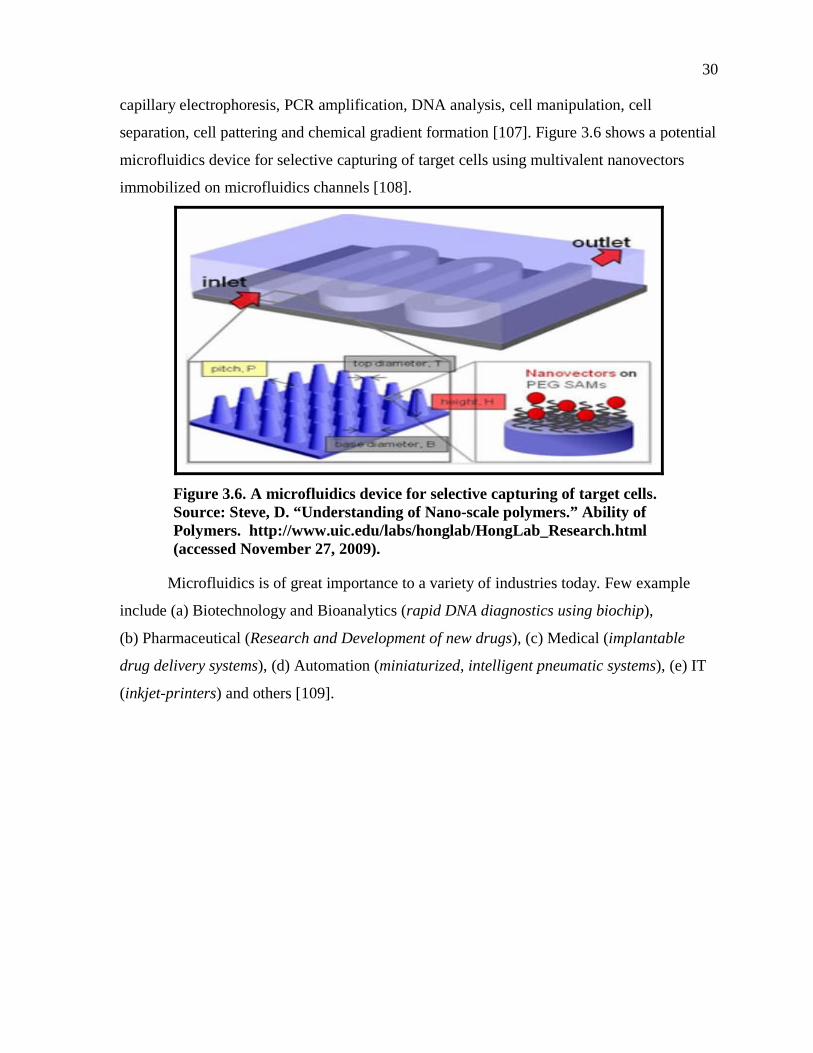
separation, cell pattering and chemical gradient formation [107]. Figure 3.6 shows a potential
microfluidics device for selective capturing of target cells using multivalent nanovectors
immobilized on microfluidics channels [108].
Figure 3.6. A microfluidics device for selective capturing of target cells. Source: Steve, D. “Understanding of Nano-scale polymers.” Ability of Polymers. http://www.uic.edu/labs/honglab/HongLab_Research.html (accessed November 27, 2009).
Microfluidics is of great importance to a variety of industries today. Few example
include (a) Biotechnology and Bioanalytics (rapid DNA diagnostics using biochip),
(b) Pharmaceutical (Research and Development of new drugs), (c) Medical (implantable
drug delivery systems), (d) Automation (miniaturized, intelligent pneumatic systems), (e) IT
(inkjet-printers) and others [109].

31
CHAPTER 4
FABRICATION OF C-MEMS MICROARRAY AND
PACKAGING UNIT
This chapter describes the step-by-step micro fabrication of the 3-D carbon
microarray using CMEMS technology. Further, design and fabrication of the packaging unit
for microarrays is discussed.
4.1 FABRICATION OF C-MEMS MICROARRAY For microfabrication of biochips for pathogen detection, a variety of
microfabrications techniques based on silicon-based or glass-based Micro-Electro-
Mechanical Systems (MEMS) technologies were introduced in the last decade [110]. In
recent years, for low cost and mass production, polymer based carbon materials have been
utilized for the microfabrication process due to good mechanical durability, electrical
conductivity, and chemical stability of carbon materials [111, 112]. These materials have
attractive properties for design of 3-D electrodes that enables high-aspect-ratio features.
The 3-D carbon microarray biochips were fabricated using the facility at MEMS
Class100 Cleanroom at San Diego State University, California. As shown in Figure 4.1, the
microfabrications of 3-D carbon microarray starts with a clean (100) silicon wafer which has
0.5µm thick silicon dioxide layer for the insulation [113].
Followed by the insulation, the wafer is spin-coated for 10µm thickness using SU-8
10 (family of SU-8, a chemically amplified negative tone photoresist based on epoxy-
novolac resin designed for micromachining and other microelectronics applications [114])
for 35 seconds at 3000rpm (Figure 4.2) and goes through the soft bake process for 7 minutes
at 95ºC in the oven. The first mask is placed on top of the soft baked wafer with an exposed
energy of 300mJ/cm2. Of the three exposure modes contact, proximity, and projection mode,
proximity lithography mode was used here which has the ability of mask that does not touch
the wafer and is fixed on top of the glass that touches the wafer. A PEB (Post Expose Bake)
process is done after the soft bake process for 4 minutes at 95ºC on the level hot plate. After
10 minutes cooling off, the wafer is developed by using SU-8 developer and then rinsed off

32
Figure 4.1. Schematic diagram of CMEMS process. Source: Madou, M. “Micro patterning of conductive polymers.” Application of polymers. http://mmadou.eng.uci.edu/Lectures/ECS2003F.ppt (accessed December 1, 2009).
by isopropanol to remove the residues. All of these above process establish an ideal electrical
connection between electrodes and bump pads. But in order to fabricate a 3-D electrode with
high aspect-ratio structures, the wafer are again spin-coated using SU-8 100 which is more
viscous than SU-8 10 for 35 seconds at 1600rpm with a thickness of 220µm.
The SU-8 100 spin-coated wafer is then soft-baked for 1.5 hours at 95ºC on the level
hot plate followed by a second lithography. This second lithography process requires a mask
aligner for the wafer, a second mask and finally UV exposure with energy of 700mJ/cm2.
The wafer is exposed for 20 minutes PEB at 95ºC on the hot plate and then is developed for
30 minutes (Figure 4.3). After all the Soft bake process and PEB, the wafer undergoes
pyrolysis, a chemical decomposition of condensed organic substance by heating schedules
(Table 4.1). The heating schedules have multi-steps to prevent the peel-off phenomenon
during pyrolysis and are done in the presence of nitrogen gas for about 10 hours [115].
Figure 4.4 shows the Scanning Electron Microscope (SEM) pictures of each chip after
fabrication.

33
Figure 4.2. Silicon wafer spin-coating. (a) dispersing photoresist on wafer and (b) wafer with SU-8 10 thickness of 10µm.
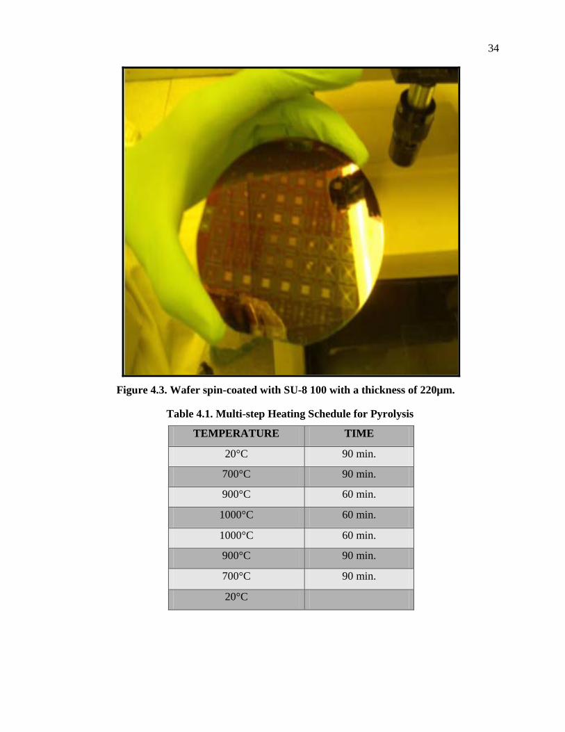
34
Figure 4.3. Wafer spin-coated with SU-8 100 with a thickness of 220µm.
Table 4.1. Multi-step Heating Schedule for Pyrolysis
TEMPERATURE TIME
20°C 90 min.
700°C 90 min.
900°C 60 min.
1000°C 60 min.
1000°C 60 min.
900°C 90 min.
700°C 90 min.
20°C

35
Figure 4.4. SEM Pictures of microarray. (a) 3x3 (b) 5x5 (c) 10x10.
4.2 PACKAGING UNIT The all-polymer biochip consists of electrodes, traces and bump pads made of the
same material (pyrolyzed SU-8) and hence during electrophoresis, the accumulation of beads
occurs at all these regions. This reduces the efficiency of the chip. In order to overcome this
difficulty and to force accumulation only at the electrodes, the traces and bump pads have to
be isolated from the buffer solution which consists of the microbeads. This gives rise to the
need of a packaging unit.
A packaging unit is a component with multiple parts assembled as a single unit to
hold and protect the microchip during experimentation and to isolate the traces and bump
pads from the solution. The packaging consists of three parts: (1) Bottom case – which acts
as a base for holding the chip (Figure 4.5), (2) Top case – provides electrical access to bump
pads which are connected to the electrodes via traces and (3) PDMS (Polydimethylsiloxane)
pressure seal – separates the traces and bump pads from the buffer solution and also prevents
leakage of the buffer solution from the packaging unit.
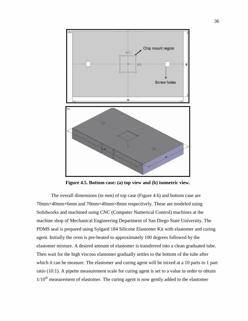
36
Figure 4.5. Bottom case: (a) top view and (b) isometric view.
The overall dimensions (in mm) of top case (Figure 4.6) and bottom case are
70mm×40mm×6mm and 70mm×40mm×8mm respectively. These are modeled using
Solidworks and machined using CNC (Computer Numerical Control) machines at the
machine shop of Mechanical Engineering Department of San Diego State University. The
PDMS seal is prepared using Sylgard 184 Silicone Elastomer Kit with elastomer and curing
agent. Initially the oven is pre-heated to approximately 100 degrees followed by the
elastomer mixture. A desired amount of elastomer is transferred into a clean graduated tube.
Then wait for the high viscous elastomer gradually settles to the bottom of the tube after
which it can be measure. The elastomer and curing agent will be mixed at a 10 parts to 1 part
ratio (10:1). A pipette measurement scale for curing agent is set to a value in order to obtain
1/10th measurement of elastomer. The curing agent is now gently added to the elastomer

37
Figure 4.6. Top case: (a) top view and (b) isometric view.
using the pipette and stirred with the pipette tip in order for the two different mixtures to mix
together. Care is taken while using the pipette because when the mixture reaches the pipette
chamber it will alter future suction function of the pipette by drying and clogging it.
The elastomer is mixed well with the curing agent for few minutes and then left till all
the bubbles disappear from the mixture. Once almost all the bubbles have cleared from the
mixture, a pipette is used to get small amount to coat the desired cavities of the PDMS
sample mold (Figure 4.7) by running slowly off the pipette tip. Again care is taken to have no
bubbles in the mold because the bubble will solidify in the baked sample. In case of bubbles
in the mold, it is removed by suctioning them out with a pipette. The mold is placed in to the
pre-heated oven with a flat paper or aluminum foil underneath the mold, to avoid sticking of
the mixture to the oven surface due to overflow. The sample is baked for approximately 10 to

38
Figure 4.7. PDMS mold case. (a) top view and (b) isometric view.
15 minutes in the oven. The solidity of the mixture is checked, if it is still slightly liquid then
it is left for few more minutes. The heat cure specifications for baking the PDMS are
described at the Dow Corning website shown in Table 4.2 [116]. Using this heat cure
specifications, PDMS is baked accordingly.
Table 4.2. Heat Cure Specifications for Baking PDMS
MINUTES DEGREE
CENTIGRADE
10 150
20 125
45 100

39
Once the mixture (PDMS) is dried, remove the sample from the oven and put them in
a freezer for few minutes. This will shrink the PDMS slightly and will help when peeling the
samples delicately out of their molds. Carefully use a scalpel blade to separate the PDMS
from a side of the mold wall so that the rest can be pulled gently from the mold. Figure 4.8
shows the assembly diagram of the bottom case, PDMS pressure seal, and top case of the
packaging.
Figure 4.8. Carbon microarray biochip packaging unit.

40
CHAPTER 5
ELECTROPHORETIC EXPERIMENTATION
This chapter describes the design and fabrication of a closed cell packaging unit used
to encompass the microarray chip for pathogen detection during experimentation. This
chapter also discusses the results of the electrophoretic experimentation using microbeads
that mimic DNA. Electrophoretic experimentation is carried out on the Signatone probe
station and is shown in Figure 5.1.
Figure 5.1. Electrophoretic experimental setup.

41
The microchip with 3×3, 5×5, and 10×10 microarrayed electrodes (circular and
diamond shaped) are used in conjunction with a closed cell packaging unit as shown in
Figure 5.2. L-Histidine buffer solution is used in which negatively charged 1.94µm
polycarboxylate beads (Polysciences, Inc.) are dispersed in it. In order to initiate the active
electrophoretic experiment, DC power is applied by triple output power supply (Hewlett-
Packard) and the experiment is observed through a microscope with a CCD camera which in
turn is connected to a 19-inch LCD monitor (Samsung).
Figure 5.2. Sketch of carbon microarrays. (a) 3×3, (b) 5×5, and (c) 10×10.

42
In order to conduct the electrophoretic experiment, 50mM Histidine buffer solution:
0.776g of Histidine with molecular weight of 155.16g/mol (conductivity: 60µS/cm) is added
to 0.1 liter of deionizer water. Negatively charged 1.94µm polycarboxylate microspheres are
dispersed in the histidine solution with a concentration of 0.42g/l. This histidine buffer
solution acts as a low-salt buffer to promote the electrophoretic transport of micro beads and
also assures uniform electric field distribution throughout the micro electrode array [49]. For
closed cell electrophoresis, a 10×10 microarrayed chip as shown in Figure 5.3 was mounted
on the packaging unit where the packaging covers most of the chip area leaving the electrode
and bump pad regions accessible.
Figure 5.3. 10×10 microarray chip.
A 5µl histidine buffer solution with dispersed microspheres is added through the
electrode access region into the flow cell. Electrical contacts to the chip from the DC source
are established using two probe needles. The needles from the probe arms are connected to
two different electrodes via bump pads with traces as shown in Figure 5.4. One probe inputs
positive voltage to the electrode, making it the anode and the other inputs negative voltage
making it a cathode. The beads are in random Brownian motion before the application of DC
voltage and when the voltage is applied, negatively charged beads start moving slowly in the

43
Figure 5.4. Biasing of bump pads through top case.
buffer solution. When the voltage reaches 4-5V, the beads start to migrate towards the
positively biased electrode. As the applied voltage is stabilized around 5V, more
accumulation of beads occurs forming a white cloud around the positively biased electrodes.
Figure 5.5 shows the step by step accumulation of negatively charged polycarboxylate beads:
(a) At 10 seconds, after biasing there is almost equal concentration of beads around the entire
chip region (b) & (c) At 30 and 60 seconds after biasing of electrodes, there is an increase in
the accumulation of negatively charged beads around the positively biased electrodes and at
the same time, repulsion of beads takes place at negatively biased electrodes (d) At 120
seconds, there is a huge accumulation around the positively biased electrodes and complete
repulsion of beads around the negatively biased region.
As the voltage is increased above 5V, bubbling hinders the accumulation of the
beads, makes the visibility poor and electrodes start to peel off from the silicon substrate
(Figure 5.6). After maximum accumulation, a reverse bias is applied i.e., the electrode that
was formerly an anode becomes a cathode and the former cathode becomes an anode. As the
accumulated beads are negatively charged in nature, they tend to be repelled from the current
cathode which was formerly the anode. Now beads start to move towards the current anode
and hence the region around the current cathode begins to deplete. The electrophoretic
experimentation during the reverse bias is illustrated in Figure 5.7.

44
Figure 5.5. Electrophoretic experimentation: Accumulation. (a), (b), (c), and (d) Showing accumulation of negatively biased beads towards anode region with respect to time.

45

46

47
Figure 5.6. Peeling of electrodes.
All the above accumulation and repulsion experiments based on electrophoretic
movement uses negatively charged micro beads. In real time, we can use DNA, RNA,
charged micro organisms, etc, to perform this electrophoresis experiments on carbon chips.
These carbon chips have an enhanced electrochemical window as voltages up to 6V
can be applied when compared to the other reported biochips with 2-D metal electrode
microarrays. Thus these 3-D carbon biochips have an increased workable range enabling
large volume samples to be analyzed.
The electrophoretic experiment is summarized in Figure 5.8 which is plotted between
time (seconds) and voltage (V). It is evident from the figure that during the initial 10 seconds
of the experiment, the negatively charged microbeads starts moving towards the positively
biased electrode for a voltage around 1-2V. As the time increases from 10-120 seconds with
an applied voltage of 4-5V, there is a maximum accumulation of beads around the anode.
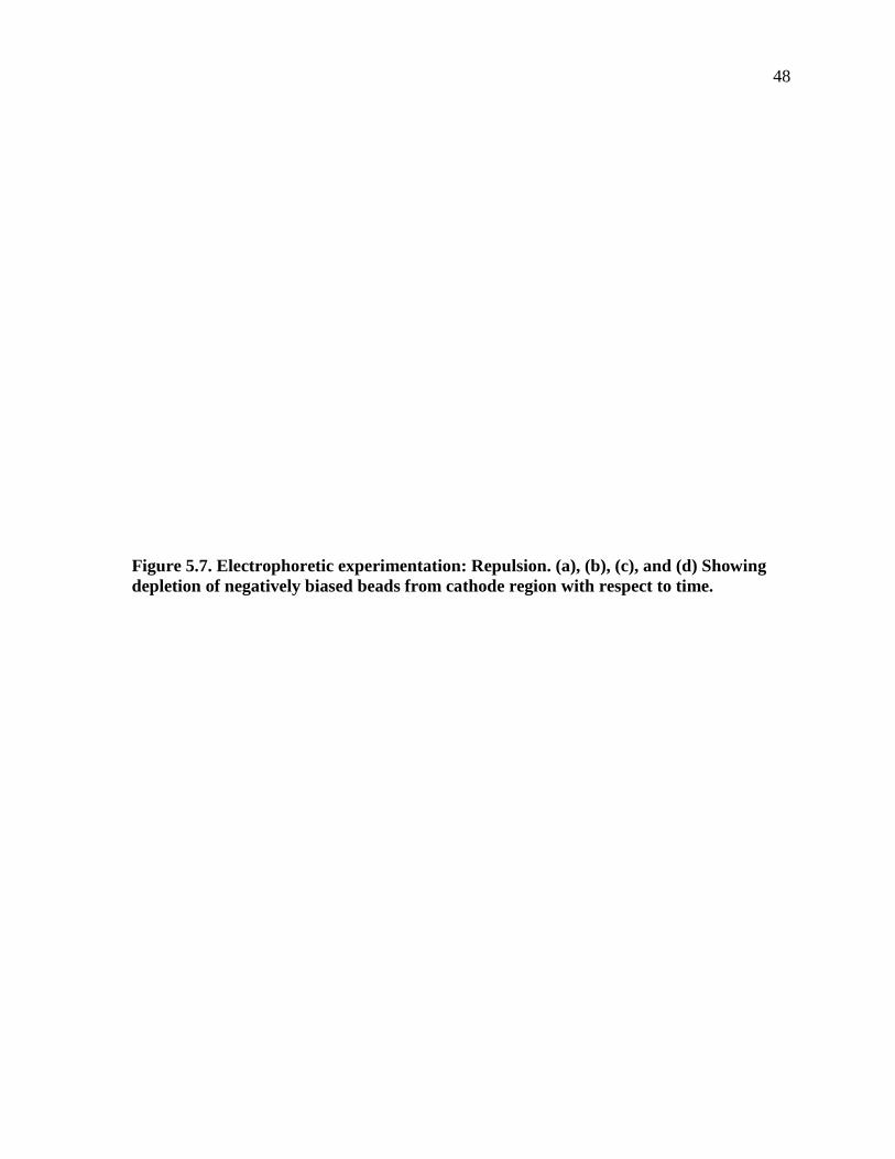
48
Figure 5.7. Electrophoretic experimentation: Repulsion. (a), (b), (c), and (d) Showing depletion of negatively biased beads from cathode region with respect to time.

49

50

51
Figure 5.8. Summary of electrophoretic experimentation.

52
CHAPTER 6
IMAGE PROCESSING AND 3-D ANALYSIS
In this chapter, image analysis of electrophoretic results is carried out using various
imaging techniques. 2-D analysis of the accumulated beads on the chip is done using Matlab
software for image processing. As these carbon electrodes are 3 dimensional in structure,
accumulation of beads along the height of the electrode is expected. In order to establish and
confirm this fact, 3-D analysis is carried out with the help of Scanning Electron Microscopy
(SEM) and Confocal Microscope on the accumulated chip. In addition a live electrophoretic
experiment is captured in real time using a Hirox Digital Microscope.
6.1 IMAGE PROCESSING USING SOFTWARE Image processing is any form of signal processing where the input is an image, such
as photographs or frames of video and the output of image processing can be either an image
or a set of characteristics or parameters related to the image. Most image-processing
techniques involve treating the picture as a two dimensional image and applying standard
signal-processing techniques to it.
In this research, videos are obtained from the electrophoretic experiments using a
charge-coupled device (CCD), a core technology used by most digital cameras. This CCD
camera consists of a series of closely spaced metal-oxide-semiconductor capacitors (MOS),
each one corresponding to a single image pixel. In its most basic form a CCD is a charge
storage and transport device where charge is stored on the MOS capacitors and then
transported across these capacitors for readout and subsequent transformation to a digital
image.
The image obtained by the CCD camera (Zarbeco, L.L.C, Randolph, NJ) is viewed
and stored using Zarbeco Video Toolbox Pro as shown in Figure 6.1 [117], which is installed
in windows vista (2 GHz, 2 GB RAM Inter (R) core duo CPU). Image processing is done
using a combination of mencoder (mplayer) and Matlab (see Appendix). A live
electrophoretic experiment is conducted and recorded as an uncompressed video in dot avi

53
Figure 6.1. Zarbeco video toolbox pro.
format (.avi). The duration of this video is about 3 minutes and is 3 GB in size. Due to the
size of the video, it cannot be uploaded as a single file for processing in Matlab.
Hence the video is made into segments whose size depends upon the configuration of
the processor used for image processing. The video is segmented into two parts using
mencoder: (i) Part 1 of the video consists of 35 seconds after accumulation begins; (ii) Part 2
of the video is 35 seconds in duration and shows the depletion process.
[Note: The duration of the video to be processed depends on the capacity of RAM in the
system]. Mencoder command line tools for segmenting a video is given below and is
illustrated in Table 6.1.
The segment to be analyzed is given as an input file to Matlab software and image
processing of the video is done using Matlab codes. When a video is processed in Matlab the
output is obtained as frames and the total number of frames in a video can be calculated as:
Total number of frames = Number of frames/sec × Length of the video in sec
A rectangular region around the biased electrodes is selected as our ROI (Region of
interest) and follows four co-ordinates system. This ROI is basically our way of telling the

54
Table 6.1. Mencoder Commands and Description
mencoder aaa.avi –ss x –endpos y -ovc copy –o bbb.avi
MENCODER COMMANDS DESCRIPTION
aaa.avi Input video file name
-ss Command for start time
x Input extract start time
-endpos Command for duration of the extract
y Input duration time
-ovc copy Command for no compression
-o Command for output file to write to
bbb.avi Output video file name to be saved
program to perform calculation only in this area and ignore everything outside this area. A
warning message is displayed when the ROI extends outside the image boundary. The region
of interest (ROI) shown in Figure 6.2 represents the parameters involved where (0, 0)
represents the (X, Y) co-ordinate of the image boundary, (70,140) and (390,140) represents
the (X, Y) co-ordinate of ROI 1 and ROI 2 respectively. (80) represents the width of the ROI
regions and (220) represents the height of the ROI regions. Once the ROI regions are
finalized, beads in these ROI regions have to be analyzed.
Figure 6.2. Region of Interest (ROI).

55
Image processing under Matlab treats every single bead as a pixel which is
differentiated from the rest of the image based on the color intensity. In order to increase the
visibility of beads, the background color is subtracted from the images. The RGB color
representation of the background is determined to be (127,127,127) hence each pixel in the
image is compared with the threshold value of (127) (intensity above which a pixel is
considered a bead). Every pixel above this intensity in the ROI is tailed as beads. The process
consists mostly of calculating various characteristics of the microbeads, or rather the pixel
representation of the bead groups. The Matlab program simply floors all the pixel intensities
thus creating a binary or two tone black and white image in which (0) represents black and
(255) represents white as in Figure 6.3. For enhanced clarity of the image, the negative of
this black and white image is considered where the beads are black in color and the
background is white in color.
Figure 6.3. Color codes.
Now the output is in the form of frames representing image at various points of time.
The frame at 0 seconds (before biasing) shows an equal concentration of beads at ROI 1 and
ROI 2 as shown in Figure 6.4. The video is processed at ROI 1 (positively biased electrodes)
from 0th second till 30th second and this produces 1500 frames. Figure 6.5 shows the 1500th
frame where there is maximum accumulation at ROI 1 and maximum depletion at ROI 2.

56
Figure 6.4. Image processing of chip showing equal concentration of beads at ROI 1 and ROI 2.
Figure 6.5. 10×10 microarray. (a) and (b) Image processing of accumulation at ROI 1 and depletion of beads at ROI 2.

57
Table 6.2 represents the accumulation concentration of beads at various times. Also, a
graph is plotted as in Figure 6.6 between time in seconds and concentration of beads
accumulated around the electrode in the ROI regions.
Table 6.2. Accumulation Concentration of Beads With Respect to Frames
Time in seconds 0 2 4 6 8 10 12 14
Concentration of Beads ( g/l)
0.42 1.16 1.25 1.27 1.28 1.30 1.3 1.29
Time in seconds 16 18 20 22 24 26 28 30
Concentration of Beads (g/l)
1.34 1.33 1.32 1.325 1.317 1.31 1.29 1.28
Figure 6.6. Accumulation of beads concentration vs. frame numbers.
It is seen from Figure 6.6 that there is a steep increase in the beads concentration
during the initial time. This represents the increase in number of beads entering the ROI1
region (anode) as the bias is applied to the electrodes. A fluctuation is observed in the graph
between 5 to 15 seconds. This is due to the fact that the beads present in the ROI1 region are

58
accumulating along the walls of the electrode creating dips in the graph due to stacking
effect. But at the same time there are other beads entering the ROI1 region which tend to
increase the number of observable beads. From 15 to 30 seconds, there is only a slight
increasing trend with less variation in the graph. This is because at this point of time, there is
maximum number of beads in the ROI1 region which are being accumulated while only a
few beads enter this region. After a while, the graph steadies out as the beads have been
accumulated reaching a threshold limit suggesting that no more beads can get accumulated
on the electrodes. This threshold limit depends on the surface area of the exposed region in
solution and the workable potential range of the electrode. Table 6.3 shows the concentration
of accumulated beads as 3.2 and Table 6.4 shows the concentration of beads in seconds. This
concentration factor can be calculated as shown in Equation 6.1.
Concentration Factor = concentration after biasing / concentration before Biasing (6.1)
Table 6.3. Concentration of Accumulated Beads
BEFORE BIASING
(Concentration of beads in g/l)
AFTER BIASING (Concentration of
beads in g/l)
INCREASE IN CONCENTRATION
FACTOR
ROI 1 0.42 1.34 3.2
Table 6.4. Increased Accumulation Concentration of Beads with Respect to Time
Time in seconds 0 2 4 6 8 10 12 14
Concentration of Beads (g/l)
1.280 1.327 1.384 1.415 1.420 1.358 1.346 1.334
NOTE: The beads stacked along the height of the electrode are not recognized during image
processing because the images in the video are considered two dimensional as the CCD
camera is placed perpendicular to the base of the chip during video capture.
In order to conform the stacking of beads on one another, positively biased polarity at
ROI 1 is changed to negative as shown in Figure 6.7. The output result clearly shows that the

59
Figure 6.7. Increased accumulation of beads vs. frame numbers.
concentration of accumulated beads is more than the accumulated beads concentration shown
in Table 6.2 and Figure 6.6. Table 6.5 shows the increased concentration of beads from a
factor of 3.2 to 3.38 and Table 6.6 shows the depletion concentration of beads with respect to
time.
Table 6.5. Increased Concentration of Accumulated Beads
BEFORE BIASING
(Concentration of beads in g/l)
AFTER BIASING (Concentration of
beads in g/l)
INCREASE IN CONCENTRATION
FACTOR
ROI 1 0.42 1.42 3.38
Table 6.6. Depletion Concentration of Beads With Respect to Frames
Time in seconds 0 2 4 6 8 10 12 14
Concentration of Beads ( g/l)
0.42 0.340 0.255 0.175 0.118 0.066 0.049 0.035
Time in seconds 16 18 20 22 24 26 28 30
Concentration of Beads (g/l)
0.036 0.029 0.030 0.029 0.028 0.027 0.025 0.022

60
Processing of the experimental electrophoresis video at 35th second (after biasing)
shows a huge accumulation of beads at positively biased electrodes (ROI 1) and very low
concentration of beads at negatively biased electrodes (ROI 2) as shown in Figure 6.8. The
image processing is made at negatively biased electrodes (ROI 2) from 0 second till 35th
second of the video which produces 1500 frames. Each frame number represents the
concentration of beads which is shown in Table 6.6. The graph is plotted between time in
seconds and concentration of beads which shows a steady decrease for some time later which
straightens. Table 6.7 shows the decreased concentration of beads as 19.09.
Figure 6.8. Depletion of beads concentration vs. frame numbers.
Table 6.7. Decreased Concentration of Accumulated Beads
BEFORE BIASING (Concentration of
beads in g/l)
AFTER BIASING (Concentration of
beads in g/l)
DECREASE IN CONCENTRATION
FACTOR
ROI 2 0.42 0.022 19.09
6.2 THREE DIMENSIONAL ANALYSIS The 2-D image analysis results indicates that there is a stacking effect during the
accumulation of beads but it does not shows how the stacking looks like or the concentration
of beads that can be accumulated around the biased electrodes. In order to clearly identify the
stacking and the quantification of beads, live 3-D electrophoresis experiment was done using

61
Hirox digital microscope followed by its imaging and quantification of beads by a SEM and
Keyence digital microscope respectively.
6.2.1. Live 3-D Experimentation: Hirox Digital Microscope
For establishing that there is accumulation along the sides of the electrode,
electrophoresis experiment is conducted and is recorded using a HIROX digital microscope
(KH-7700, River Edge, NJ) capable of recording live experiments on a real time basis
(Figure 6.9). The microscope is incorporated with rotating mirrors that enable three
dimensional profiling of the electrodes [118].
Figure 6.9. Hirox digital microscope.
Figure 6.10 shows the electrodes during accumulation and repulsion of beads. Thus it
is seen from the figures that there is an accumulation along the walls of the electrode.
Layered stacking of beads is expected around the biased region and hence to analyze this, a
scanning electron microscope is used.

62
Figure 6.10. 3-D electrophoretic experiment. (a) accumulation and (b) repulsion.
6.2.2. 3-D Analysis Using Scanning Electron Microscope (SEM)
In order for the chip to be suitable for analysis using SEM, certain steps need to be
followed to keep the microbeads in position around the electrode. Once the electrophoretic
experiment is carried out, the 3-D carbon chip is left in the experimental setup environment
with the positive and negative electrodes biased. Under this condition, the buffer solution is
made to dry and the dried chip is analyzed under Scanning Electron Microscope (Hitachi S-
2700, EM facility at SDSU). The typical specimen to be analyzed under SEM is coated in
gold to make it conductive. As the 3-D biochips are made of conductive Carbon, it can be
readily used without the need for gold coating. The chip is viewed under the microscope and
images are obtained at various regions of the chip.
Figure 6.11, shows accumulated beads on the positively biased 3-D electrodes on the
Carbon chip during electrophoresis. A closer view of the accumulated beads on the trace
between two electrodes is shown in Figure 6.12 and Figure 6.13.

63
Figure 6.11. SEM image showing the accumulated beads around the 3-D electrodes.
Figure 6.12. SEM image of accumulated beads on trace between two electrodes.

64
Figure 6.13. Closer view of the beads on trace between two electrodes.
Figure 6.14 shows the SEM image of the beads accumulated on the trace. The picture
portrays two distinct layers of beads in this region. This phenomenon of beads accumulating
over each other is known as stacking effect. A similar phenomenon is observed even at the
electrode region but to a greater extent. Figure 6.15 shows a SEM image of stacking of beads
around the electrode region. Further, the accumulation of microbeads along the walls of the
electrode is also observed.
SEM imaging was done on the four sides (front, rear, left, and right) of a single
accumulated electrode in order to show the uniform accumulation of negatively charged
beads on the 3-D walls of positively biased electrode as shown in Figure 6.16. These pictures
establish the fact that the Carbon chip is capable of accumulating the beads along the z-
direction in a uniform manner.
Figure 6.17 shows a comparison of negatively biased electrode and positively biased
electrode, where (a) shows an electrode with no beads on it due to the negative bias which
repels the negatively charged beads, and (b) shows a huge accumulation of beads due to the
positive bias which accumulates negatively charged beads.

65
Figure 6.14. Image of individual beads under SEM.
Figure 6.15. SEM image showing the stacking of beads along the walls of the electrode.

66
Figure 6.16. SEM image showing the accumulation at anode. (a) front view (b) rear view (c) left view and (d) right view.
Figure 6.17. SEM image of 3-D electrodes. (a) negatively biased electrode without beads and (b) positively biased electrode with beads.

67
SEM imaging is also made at the top portion of the positively and negatively biased
electrodes to see whether the accumulation only occurs along the walls, traces and trace-
electrode intersections of the positively biased region. Interestingly, there was significant
amount of accumulation on the top portion of the positively biased electrode. Figure 6.18
compares the top view of (a) negatively biased electrode without negatively charged beads,
and (b) positively biased electrode with accumulation of negatively charged beads.
Figure 6.18. SEM image showing top view of the electrode. (a) without beads, and (b) with beads.
As the beads are stacked on top of one another, when 2-D image analysis is made in
this region the result only includes the top layer of beads and those beads under the top layer
are not taken into consideration. Hence during image processing of electrophoretic
experiments, the accumulation of bead concentration remains same even thought the actual
accumulation was much higher. This is due to the stacking of beads on one another which is
evident from the shape of the graph in Figure 6.6 that explains the accumulation of beads
concentration vs. frame numbers.
Usually when an electric field is applied to the electrodes, beads are attracted towards
the positively biased electrodes. Analyzing the above SEM images, we can define three
possibilities of beads stacking which is shown in Figure 6.19: (a) Worst case scenario where

68
Figure 6.19. Types of accumulation of beads.
the beads are stacked one over the other with a height of 3.88µm (size of a single bead = ~
1.94µm), (b) Second layer of beads stacked between the gaps in the first layer with a height
of 3.39µm and is the most commonly seen arrangement. (c) Where the edge of the second
layer of beads aligns with the midpoint of the beads in first layer with a height of 2.91µm.
Hence for a given height of accumulation of beads, case (a) contains the least number of
stacks while case (c) contains the maximum number of stacks.
In this section, the SEM images show that there is accumulation along the walls of the
electrode as well as stacking of beads around the electrode. In order to quantify the amount
of accumulated beads, we use a 3-D profiler with built in software. In this profiling, we
consider the worst case scenario (Figure 6.19 (a): 3.88µm) of beads stacking as the results
obtained will have the least number of stacks for a given height of accumulation.
6.2.3. 3-D Analysis Using Keyence Digital Microscope In this section, profiling of beads on the electrode and trace is done using a Keyence
digital microscope (VHX-600, Woodcliff Lake, NJ) which is shown in Figure 6.20. The

69
Figure 6.20. Keyence. “Sensors, vision, measurement and microscopes.” Innovation in 3-D microscopes. http://www.keyence.com/ (accessed April 18, 2010).
microscope can be used for analyzing highly reflective surfaces and measurement of height,
width and height difference data on a given cross section is made possible [119]. Figure 6.21
shows an image of the accumulated beads on a 10×10 chip using VHX-600 digital
microscope: (1) across the trace, (2) around the electrode, and (3) height of the electrode.
Figure 6.21. Profiling of the accumulated chip.

70
6.2.3.1 PROFILING ACROSS THE TRACE A section of the accumulated trace between two electrodes is considered for profiling
as shown in Figure 6.21. The profiling is done at two spots (1 and 2). At spot 1, the height of
the bead from the base of the chip is 1.84µm as compared to the spot 2, which measures the
height as 3.67µm. This profiling gives a clear picture of two layer stacking on the traces
between two electrodes as shown from the profiling graph shown in Figure 6.22.
Figure 6.22. Profiling across the trace.
Calculation for number of beads on the trace:
Average diameter of a single bead (D bead) = 1.94µm
Height of the beads stack on the trace = 3.67µm (6.2)

71
From Equation 6.2,
Number of stacks on the trace = Height of the beads stack on the trace / D bead
= 3.67 / 1.94 = 1.89
Hence, number of stacks on the trace = ~2 stacks (6.3)
Assume a square area of 100µm × 100µm
Number of beads in a square area of 100×100 µm2 with single stack of beads at trace (T1)
= ((Length × Breadth) / (D bead) 2)
= (100 × 100)/1.942
T1= ~ 2577 beads
From Equation 6.3, we know the total number of stacks on the trace is ~2. So, number of
beads in a square area of 100×100µm2 with two stacks of beads at trace (T2)
= T1 × 2
= 2577 × 2
T2 = ~5154 beads
6.2.3.2 PROFILING ACROSS ELECTRODES A region around the accumulated electrode is considered for profiling as shown in
Figure 6.23. This profiling not only shows the presence of accumulated beads along the walls
of the 3-D electrode, but it also reveals that there are numerous layers of stacks.
Calculation for beads stacks around the electrode:
From the graph,
Maximum height of the accumulation around the 3-D electrode (H max Accum) = 28.2µm(6.4)
Using Equation 6.4,
Number of stacks possible at maximum accumulation (S max Accum) = H max Accum / D bead
= 28.2/1.94
S max Accum = ~15 stacks (6.5)

72
Figure 6.23. Profiling around the electrode.
6.2.3.3 PROFILING 3-D ELECTRODE The profiling of the 3-D electrode is shown in Figure 6.24.
The height calculated from the graph = 95.5µm (6.6)
This represents the height from the top layer of the beads on the trace to the top layer of
beads on the electrode. Also, it is seen from the graph that there is accumulation on the walls
of the electrode which extends to a certain length around the 3-D electrode. Hence, total
accumulation length at the base (L tot Accum) is calculated from the graph as 147µm.
L tot Accum = 147µm (6.7)
From the graph (Figure 6.24),

73
Figure 6.24. Profiling 3-D electrode.
Height of the accumulation on the top surface of 3-D electrode (H top Accum) = ~7.76µm(6.8)
Number of stacks possible at top surface of 3-D electrode (S top Accum) = H top Accum / D bead
= 8/1.94
S top Accum = ~4 stacks (6.9)
6.3. QUANTIFYING BEADS ALONG THE WALLS OF 3-D ELECTRODE
When the profiling is made for the accumulation of beads around the electrode, the
number of stacks is not same along the full height of the electrode. From equation 6.5, it is
clear that the electrode has ~15 stacks around it up to a height of 28.2µm. Above this height,
it is seen from the Figure 6.16 that there is only a single stack of beads.
Using Equations 6.2, 6.6, and 6.7, we find the height of the electrode. We know from
Equation 6.6 that the height from the top layer of the beads on the trace to the top layer of
beads on the electrode is 95.5µm. This includes the height of beads accumulated on the top

74
surface of the electrode which is 7.76µm. Also, from Equation 6.2, we know there is two
stack beads accumulation to a height of 3.67µm.
Height of the electrode = Equation 6.6 – Equation 6.8 + Equation 6.2 + height of the trace
= 95.5µm – 7.76µm + 3.67µm + 2µm
H elec = 93.41µm (6.10)
From this we can calculate the height up to which there is single stacking of beads.
Using Equations 6.4 and 6.10,
Height up to which there is single stacking (H elec single) = H elec - H max Accum
= 93.41 µm - 28.2 µm
H elec single = 65.21µm (6.11)
6.3.1 Calculation for Beads Stacks along the Walls of the 3-D Electrode
The schematic representation of the beads accumulated at the base of the electrode is
shown in Figure 6.25.
Figure 6.25. Schematic representation of beads at the base of the electrode.

75
From Equation 6.7, total accumulation length at the base (L tot Accum) = 147 µm = D outer
From Figure 6.25, Total effective accumulation length at the base (L tot eff) = D outer – D inner
= 147 – 95
L tot eff = 52µm (6.12)
Using Equation 6.12,
Hence, Effective accumulation length at the base on one side (Leff) = L tot eff / 2
= 52/2
L eff = 26µm (6.13)
From Equation 6.4, Maximum height of the accumulation around the 3-D electrode
(H max Accum) = 28.2µm, across section A-A in Figure 6.25 (a), it is seen that the number of
bead stacks decreases away from the 3-D electrode. So in order to calculate the number of
beads in this region, we integrate the area of the triangle (shape of region formed by
accumulated beads) as in Figure 6.26.
Figure 6.26. Beads accumulated at the base of the electrode represented as a triangle ABC.
A = ∫ f(x) dx
= 0∫b (slope of line AC) dx = 0∫b (hx/b) dx
= h/b [x2/2] 0 28.2
From Equations 6.4 and 6.13, h = 28.2 and b = 26
= 28.2/26 [{(28.2) 2 / 2} – [0]]

76
Integrated area of the triangle (ABC) = 431.26µm2 (6.14)
Using Equation 6.14,
Number of beads in this area (N triangle) = Integrated area of the triangle (ABC)/ (D bead) 2
= 431.26 / (1.94)2 = 222.30
N triangle = ~222 beads
Effective perimeter of the base (P eff base) = 2πr = 2πLeff
= 2 × 3.14 × 26 (from Equation 6.13, L eff = 26µm)
P eff base = 163.28µm
Number of beads along the perimeter (N peri base) = P eff base / D bead
= 163.28 / 1.94
N peri base = ~84 beads
Total number of beads in the region around the base of electrode (N elec base)
= N triangle × N peri base
= 222 × 84
N elec base = 18648 beads (6.15)
6.4. CALCULATION OF BEADS ON 2-D ELECTRODE A calculation of the number of beads in 2-D electrode is done based on the
assumption that the thickness of 2-D electrode is 2µm which is same as that of trace. Hence
the number of beads accumulated on 2-D electrode would be similar to the accumulation on
the traces in the 3-D biochip. The schematic representation of 2-D electrode is shown in
Figure 6.27.
Figure 6.27. Schematic representation of 2-D electrodes.
The diameter of the electrode = 95µm
Number of beads on a 2-D electrode (N single 2-D) = Area of the 2-D electrode/ (D bead) 2

77
= π r2 / (D bead) 2
= 3.14 × (47.5) 2/ (1.94) 2
N single 2-D = ~1882 beads (6.16)
From Equation 6.3, we know that the number of stacks on the trace is 2. Since the
accumulation on 2-D electrode is similar to that on the trace, the number of stacks on the 2-D
electrode is also equal to 2. Total number of beads on the top of the 2-D electrode (N tot 2-D)
= Number of beads on a 2-D electrode with single stacking × total number of stacks
= 1882 × 2
N tot 2-D = 3764 beads (6.17)
6.5. CALCULATION OF BEADS ON 3-D ELECTRODE The schematic representation of 3-D electrodes is shown in Figure 6.28.
Figure 6.28. Schematic representation of 3-D electrodes.
Top of the electrode
Number of beads on the top of the electrode in a single layer (N top single)
= Area of the 2-D electrode/(D bead) 2
= π r2 / (D bead) 2
= 3.14 × (47.5) 2/ (1.94) 2
N top single = 1882 beads
From Equation 6.9, number of stacks possible at top surface of 3-D electrode (S top Accum) = 4
Total number of beads on the top of the 3-D electrode (N top 3-D)

78
= Number of beads in single layer × Total number stacks
= N top single × S top Accum
= 1882 × 4
N top 3-D = 7528 beads (6.18)
Walls of the electrode:
From Equation 6.11, we have
The height up to which there is single stacking (H elec single) = H elec - H max Accum
That is, H elec = H max Accum + H elec single
= 28.2 µm + 65.21 µm (Equations 6.4 and 6.11)
Hence we can split the electrodes in to two regions, namely Region 1 and Region 2.
i.e., Total height of the electrode = Region 1 + Region 2
Region 1
From Equation 6.15,
Total number of beads in the region around the base of electrode = (N elec base) = N region 1
N elec base = N region 1=18648 beads (6.19)
Region 2
From Equation 6.11, we know that for 65.21µm from the top of the electrode there is only a
single layer of beads collection
Number of beads across the perimeter of the electrode = 2πr/ D bead
= 2 x 3.14 x (47.5/1.94) = 153.76
Number of beads across the perimeter of the electrode = ~154 beads (6.20)
Number of beads for a height of 65.21µm
= Height up to which there is single stacking (H elec single)/D bead
= 65.21/1.94
Number of beads for a height of 65.21µm = 34 beads (6.21)

79
Total number of beads in region 2 (N region 2) = Number of beads across the perimeter of the
electrode × Number of beads for a height of 65.21µm
= 154 × 34 (Equations 6.20 and 6.21)
N region 2 = 5236 beads
6.6 COMPARISON OF 2-D AND 3-D ELECTRODES 2-D ELECTRODE:
Bead concentration on a single 2-D electrode:
For a single stack of beads,
Total concentration of beads = 1882 beads.
For a double stack of beads,
Total number of beads concentration on the 3-D electrode (N tot 3-D)
= Single stack of beads × 2
= 1882 × 2
N tot 2-D = 3764 (6.22)
3-D ELECTRODE:
Bead concentration on a single 3-D electrode:
Using Equation 6.18 and 6.19,
Total number of beads concentration on a single 3-D electrode (N tot 3-D)
= N top 3-D + N region 1 + N region 2
= 7528 + 18648 + 5236
N tot 3-D = 31412 beads (6.23)
Using Equation 6.22 and 6.23,
Efficiency of bead accumulation (Ea) = N tot 3-D / N tot 2-D
= 31412 / 3764
Ea= 8.35
This efficiency of bead accumulation shows that the 3-D electrodes have 8 times higher
beads accumulation capacity than 2-D electrodes.

80
CHAPTER 7
FINITE ELEMENT ANALYSIS
In this research a 10×10 microarray of 150µm diameter glassy carbon electrodes
spaced with 350µm center-to-center spacing is used for numerical modeling as shown in
Figure 7.1. The numerical modeling is based on finite element formulations for electrostatic
conductive media DC and electrokinetic transient flow using FEMLAB 3.5 (developed by
Comsol. Burlington, MA).
Figure 7. 1. Schematic representation of 10×10 microarray.
The buffer solution used here is a 50mM histidine with a conductivity of 0.6µS/m, the
DNA diffusion coefficient of 6.8×10⁻¹¹ m2/s, and DNA electrophoretic mobility of
15,000µm2 /Vs [49]. One array of electrodes is biased positive and one array of electrodes is
biased negative. Typically, the anode is biased at +2.5V and cathode at -2.5V. As only two
arrays of electrodes are required for analysis, we developed a model with two arrays of

81
electrodes. Finite element simulation consisted of finite element mesh for the chip size of
1×1cm with the mesh being denser at electrodes due to sharp corners in the geometry and due
to high gradient of electric fields at these locations.
For conductive media DC, the boundary conditions used are as follows:
(i) Sides of the chip: Electric insulation.
(ii) At anode: Electric potential (+2.5V)
(iii) At cathode: Electric potential (-2.5V)
For electronically active microarray the electric field is the driving force for
transportation, accumulation, and hybridization of species in buffer solution. The result is
presented in terms of the electric field and electric potential between the positive and
negatively biased electrodes.
Figure 7.2 shows the electric field distribution between the two arrays of electrodes
i.e. anode and cathode. A more complete picture of the electric field inside the microarray, a
sectional plot along horizontal section A-A is given in Figure 7.3.
Figure 7.2. Electric field distribution in 2-D electronically active 10×10 microarray.

82
Figure 7.3. Electric field distribution across section A-A.
Figure 7.4 shows the electric potential distribution at the surface between the two
arrays of electrodes i.e. anode and cathode. A more complete picture of the electric potential
inside the microarray, a sectional plot along horizontal section B-B is given in Figure 7.5
showing a smooth electric potential distribution.
Figure 7.4. Electric potential distribution in 2-D electronically active 10×10 microarray.

83
Figure 7.5. Electric potential distribution across section B-B.
For electrokinetic flow, the boundary conditions used are as follows:
1. Sides of the chip: Insulation
2. At anode: Flux discontinuity
3. At cathode: Continuity
Finite element modeling for the concentration of DNA accumulation is solved
assuming an initial DNA concentration of 50µmoles/m3 [49]. Figure 7.6 shows the
accumulation concentration of DNA at the edge of the electrode (anode) with respect to time.
Figure 7.6. Accumulation concentration at anode.

84
Comparing the FEA result shown in Figure 7.6 with electrophoretic experimental
result shown in Figure 6.6, the results clearly indicate that the electrophoretic experiment on
a 3-D microarray biochip matches the accumulation concentration around anode which is
shown in Figure 7.7.
Figure 7.7. Comparison of FEA and experimental results on concentration beads at anode.

85
CHAPTER 8
RESULTS AND DISCUSSIONS
This chapter discusses the comparison of 2-D and 3-D carbon microarray biochips
based on the experimental results.
8.1 CONCENTRATION OF ACCUMULATION BASED ON IMAGE PROCESSING TECHNIQUES
We compare our results with that of Kassegne et al. as follows: Kassegne et al.
developed a numerical modeling of transport and accumulation of DNA on electronically
active biochips as shown in Figure 8.1. The single electrode system used in their study
consists of 25 anodes with diameter of 80µm and thickness of 100 nm. A 10µl sample (5nM
fluorescent labeled T12 oligonucleotide in 50mM histidine) was taken for analysis [49].
From Table 8.1 [49], their results show that the concentration of accumulation on a 2-D
metal electrode is 1%.
Figure 8.1. Active DNA chip: 25-site chip. Source: Kassegne, S., A. Hodko, M. Madou, K. Sarkar and J. Yang. “Numerical modeling of transport and accumulation of DNA on electronically active biochips.” Sensors and Actuators B: Chemical 94, no. 3 (2003): 81-98.
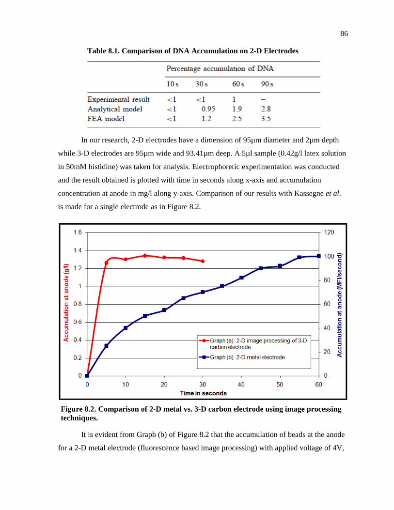
86
Table 8.1. Comparison of DNA Accumulation on 2-D Electrodes
In our research, 2-D electrodes have a dimension of 95µm diameter and 2µm depth
while 3-D electrodes are 95µm wide and 93.41µm deep. A 5µl sample (0.42g/l latex solution
in 50mM histidine) was taken for analysis. Electrophoretic experimentation was conducted
and the result obtained is plotted with time in seconds along x-axis and accumulation
concentration at anode in mg/l along y-axis. Comparison of our results with Kassegne et al.
is made for a single electrode as in Figure 8.2.
Figure 8.2. Comparison of 2-D metal vs. 3-D carbon electrode using image processing techniques.
It is evident from Graph (b) of Figure 8.2 that the accumulation of beads at the anode
for a 2-D metal electrode (fluorescence based image processing) with applied voltage of 4V,

87
there is a gradual accumulation over 60s whereas for the 3-D carbon electrode (pixel based
image processing) in graph (a), it is seen that for an applied voltage of 4-5V, there is
maximum accumulation around 10s which steadies within 25s of time. But around 30-35s
there is a decrease in concentration due to layered stacking of beads around the anode. This
phenomenon of decrease in concentration observed in the curve is due to the inability of 2-D
image processing which does not account for the stacking of beads. Even though the 2-D
image processing on a 3-D carbon chip does not provide the actual concentration of beads
around the anode, it clearly establishes the fact that 3-D carbon microarrayed biochip is more
efficient than 2-D metal chip in terms of concentration of accumulation.
In order to quantify the actual concentration of accumulation, 3-D image analysis
techniques are described in Section 8.2.
8.2 CONCENTRATION OF ACCUMULATION USING IMAGE ANALYSIS TECHNIQUES
In this section, image analysis using the profiling capability of Keyence digital
microscope and SEM are discussed.
The polycarboxylate micro-spheres (Polysciences Inc, PA) are dispersed with a
concentration of 2.64 % solids in latex solution, i.e., 0.0264g of beads/ml in latex solution.
Further we know that one gram by weight contains 2.27 × 10¹¹ beads, where average weight
of a single bead is 4.41 × 10⁻⁶µg. A flow cell solution is prepared with a concentration of
0.42µg/µl of beads in 50mM histidine buffer solution. Electrophoretic experimentation is
conducted by applying a potential difference of 4-5V at the anode and cathode. There is an
accumulation of negatively charged beads around the anode and this is quantified using a
Keyence digital microscope and SEM as in Section 6.2, 6.4, and 6.5 of Chapter 6 for 2-D and
3-D electrodes respectively. In order to compare the efficiency of a 3-D microarrayed chip
with that of the 2-D microarray chip, the bead concentration in a flow cell is calculated as
follows:
Number of beads per ml of latex solution [120]: (6W × 1012) / (ρ × π × Φ3) (8.1)
Where: W = grams of beads per ml in latex (0.0264g for a 2.64 % latex)
Φ = diameter in microns of latex particles (1.94)

88
ρ = density of polymer in grams per ml (1.05 for carboxylate)
From Equation 8.1,
Number of beads per ml of latex solution = (6 × 0.026 × 1012) / (1.05 × 3.14 × 7.30)
Number of beads per ml of latex solution = 5.68 × 10⁹ beads (8.2)
Size of flow cell: 5µl (Histidine + Latex solution with beads)
Concentration of latex solution in flow cell: 1.64% = 0.082µl
No of beads in flow cell (N Flow cell) = no of beads in 0.082µl latex solution
= 0.47 x 10⁶ beads (calculated from Equation 8.2)
Concentration of beads in 5µl flow cell solution = weight of single bead × N Flow cell
= 4.41 × 10-6 × 0.47 x 106
= 2.1µg of beads
Concentration of beads (C Flow cell) = 0.42 g of beads per liter of solution (8.3)
Increase in concentration factor (Cf 2-D beads) = Concentration of beads in accumulated region
Initial concentration of beads in flow solution (8.4)
From Equation 6.22,
Total number of beads accumulated on a single 2-D electrode: N tot 2-D = 3764 beads
In a flow cell there are five electrodes (N 2-D beads) = 3764 × 5 = 18820 beads (8.5)
Concentration of accumulated beads in region of accumulation (0.16µl*)
= weight of single bead × N 2-D beads
= 4.41 × 10-6 × 18820
= 0.083µg of beads in 0.16µl.
Hence, concentration of accumulated beads in 1 liter (C 2-D beads) = 0.52g/l (8.6)
*Note: In order to calculate the concentration of beads at the accumulated region, the volume
of solution in the region of accumulation is considered i.e. 0.16µl.
Applying Equation 8.3 and 8.6 to Equation 8.4,

89
Increase in concentration factor = 0.52 / 0.42
Cf 2-D beads = 1.24 (8.7)
From Equation 6.23,
The total number of beads accumulated on a single 3-D electrode: N tot 3-D = 31412 beads
In a flow cell there are five electrodes (N 3-D beads) = 31412 × 5 = 157060 beads(8.8)
The concentration of accumulated beads in region of accumulation (0.16µl)
= weight of single bead × N tot beads
= 4.41 × 10-6 × 157060
= 0.7µg of beads
Hence, concentration of accumulated beads in 1 liter (C 3-D beads) = 4.38g/l (8.9)
Applying Equation 8.3 and 8.9 to Equation 8.4,
The increase in concentration factor = 4.38 / 0.42
Cf 2-D beads = 10.43 (8.10)
In order to calculate the accumulation percentage, we define percentage accumulation
as the number of beads accumulated at an electrode divided by the total number of beads in
the flow cell, and is given by:
Accumulation (%) = (N 2-D beads / N Flow cell) × 100 (8.11)
Applying to Equation 8.11,
2-D Accumulation (%) = (N 2-D beads / N Flow cell) × 100
= (18820/0.47 x 106) × 100
2-D Accumulation (%) = 4 (8.12)
Applying to Equation 8.11,
3-D Accumulation (%) = (N 3-D beads / N Flow cell) × 100
= (157060/0.47 x 106) × 100

90
3-D Accumulation (%) = 33.42 (8.13)
From Equations 8.5 - 8.13, concentration of beads accumulated is given in Table 8.2.
Table 8.2. Concentration of Beads: 2-D vs. 3-D
Number of Beads
Accumulation (%)
Concentration of Beads (g/l)
Increase in concentration
factor 2-D Electrodes 18820 4 0.52 1.24
3-D Electrodes 157060 33.42 4.38 10.43
It is seen from Table 8.2 that for a flow cell concentration of 0.42g/l, the
concentration of accumulation is quantified for 2-D electrodes as 0.52g/l and for 3-D
electrodes as 4.38g/l. The results show that 3-D carbon electrodes exhibits 8.4 times higher
concentration of accumulation than 2-D carbon electrodes.
8.3 COMPARISON OF 2-D VS. 3-D ELECTRODES This section summarizes the results of 2-D image processing as well as 3-D image
analysis. The results from Figure 8.2 and Table 8.1 are plotted based on accumulation
concentration of beads at anode in g/l as shown in Figure 8.3.
Figure 8.3. Accumulation concentration of beads at anode. The ‘*’ notation for the result from [49] depicts that this concentration value has been normalized against results given in Figure 8.2 for comparison purposes.

91
It is seen from Figure 8.3 that image processing based 3-D carbon electrode has a
higher accumulation concentration than the image processing based 2-D metal electrode.
Further, the concentration of accumulation increases from 0.42g/l to 1.25g/l in 2-D carbon
electrodes whereas in 3-D carbon electrodes there is 10.5 times increase in concentration
from the base concentration, i.e. from 0.42g/l to 4.38g/l.
Also from graph (a) of Figure 8.2, it is seen that a saturation limit is attained faster
than in graph (b) due to higher applied voltage. This ability of 3-D carbon chip to withstand
higher voltage is comparable to the results obtained from electrochemical characterization on
3-D carbon microarray [121] and is shown in Figure 8.4.
Figure 8.4. Workable window of 2-D metal vs. 3-D carbon electrode. Source: Tata, N. “Electrochemical characterization of new generation 3D carbon electrode microarray.” MS diss., San Diego State University, 2010.

92
CHAPTER 9
CONCLUSION
The efficiency of 3-D C-MEMS fabricated biochip for accumulation of 1.94 µm
negatively charged polycarboxylate micro beads has been analyzed and reported in this
research. Manipulation of charged particles in microarray was carried out based on the
concept of active electrophoresis. The electrophoretic cell has a buffer solution of 50mM
Histidine solution with a concentration of 0.42g/l of beads dispersed in latex solution. A
closed cell packaging unit made from acrylic material with a PDMS pressure seal was
designed and fabricated for electrophoretic experimentation. During experimentation, the
negatively charged micro-spheres were accumulated around the positively biased electrode
due to the applied potential difference.
The following significant results were found in this research: 2-D analysis using
Matlab programming shows that at the anode, after electrophoretic experiment, there was 3.2
times increase in concentration of beads from initial concentration. Applying reverse polarity
to the accumulated region, there was 3.38 times increase in concentration of beads from
initial concentration. This gives rise to the possibility of presence of multiple stacks of beads
around the electrode. 3-D analysis using digital microscope with profiling software and
optical analysis shows that in 3-D carbon electrodes, there is 10.5 times increase from initial
concentration of beads i.e., 0.42g/l to 4.38g/l. 3-D carbon electrode has 8.4% higher
efficiency of bead accumulation than 2-D carbon electrode i.e., 0.52g/l to 4.38g/l. The
concentration of accumulation increases from 1.32g/l in 2-D metal electrodes to 4.38g/l in 3-
D carbon electrodes. The saturation level is attained at a faster rate in 3-D carbon electrodes
compared to 2-D metal electrodes. It is evident from image processing and image analysis
that the 3-D carbon electrodes are more efficient than 2-D electrodes in applications
involving high volume samples for pathogen detection systems. The electric field distribution
from finite element analysis shows that there is a higher electric field along the edges of the
biased electrodes. The numerical analysis shows a higher potential around the biased
electrode region and reduces further away from the electrode (as expected). The
93
concentration profile of accumulation of DNA using finite element modeling shows an
increase in concentration at the edge of the electrode with time.
This research involved drying of the flow cell with accumulated beads around
electrodes for quantification. This might have resulted in loss of beads from the walls of
electrode.
Future research can be done in the following areas: Live image analysis using
fluorescent beads during electrophoretic experimentation which would result in a more
precise value of accumulation concentration. The traces could be covered with insulator such
as polyamide to limit the concentration to the electrode only. Actual DNA instead of beads
could be used to get more realistic results.

94
REFERENCES
[1] Feynman, R. “There’s plenty of room at the bottom.” An Invitation to enter a new field of physics. http://www.zyvex.com/nanotech/feynman.html. (accessed October 1, 2009).
[2] Young, G. “Microelectromechanical systems.” Sandia national laboratory. http://en.wikipedia.org/wiki/microelectromechanical_systems (accessed October 3, 2009).
[3] Kassegne, S. “Microelectro Mechanical Systems.” MEMS application, ME 585 lecture notes, San Diego State University, 2007.
[4] Madou, M. “Carbon MEMS.” Significance of C-MEMS in the initial development of MEMS. http://mmadou.eng.uci.edu/Research.html. (accessed October 4, 2009).
[5] Micronit, R. “Lab-on-a-chip.” Invention of microtechnology for realizing semicounders. http://en.wikipedia.org/wiki/Microarray (accessed October 7, 2009).
[6] Ramsay, G. “DNA Chips: State-of-the-art.” Nature Biotechnology 16, no. 1 (1998): 40-44.
[7] Pethig, R. “Dielectrophoresis Using Inhomogeneous AC Electrical Fields to Separate and Manipulate Cells.” Criical Reviews in Biotechnology 16, no. 4 (1996): 331-348.
[8] Gascoyne, P., and J. Vykouval. “Electrophoresis: Its applications.” Biosensors and Bioelectronics 23, no. 13 (2003): 1973-1983.
[9] Villas, E. “Cell Electrophoresis.” Biosensors and Bioelectronics 23, no. 4 (1998): 56-61.
[10] Kassegne, S., R. Howard, P. Swanson, M. Yang, D. Smolko, H. Dalibor, D. Raymond, and M. Madou. “A Micro Electro-Optical DNA Array Sensor.” SPIE Conference on Smart Structures and Materials 26, no. 3 (2002): 4-8.
[11] Lu, Y., M. Andrew, L. Ying, K. Chen, L. Cheng, and C. Yang. “Three-dimensional electrode array for cell lysis via electroporation.” Biosensors and Bioelectronics 22, no.4 (2006): 568-574.
[12] Honda, N., M. Inaba, T. Katagiri, S. Shuichi, S. Hirotaka, H. Takayuki, O. Tetsuya, S. Mikiko, J. Mizuno, and W. Yasuo. “High efficiency electrochemical immuno sensors using 3D comb electrodes.” Biosensors and Bioelectronics 20, no. 11 (2005): 2306-2309.
[13] Tay, F., Y. Liming, J. Pang, and I. Ciprian. “Electrical and thermal characterization of a dielectrophoretic chip with 3D electrodes for cells manipulation.” Electrochemical Actuators 52, no. 8 (2007): 2862-2868.
[14] James, E. “Capillary electrophoretic methods to detect new biological compounds.” Capillary in detection method. http://www.patentstorm.us/patents/6299747.html (accessed October 3, 2009).

95
[15] Imisides, J., and G. Wallace. “Microsensors based on conducting polymers.” Chemtech 26, no. 5 (1996): 19-25.
[16] Wilson, J., C. Strout, T. DeSantis, J. Stilwell, A. Carrano, and G. Andersen. “ Sequence- specific identification of 18 pathogenic microorganisms using microarray technology.” Molecular and Cellular Probes 16, no. 2 (2002): 119-127.
[17] Wang, S. “The packaging, design, and experimental evaluation of a MEMS electrophoretic systems.” MS diss., San Diego State University, 2006.
[18] Bashir, R. “BioMEMS: state-of-the-art in detection, opportunities and prospects.” Advanced drug delivery reviews 56, no. 11 (2004): 1565-1586.
[19] Sibley, G. “DNA-DNA hybridization.” Study of complex microbial ecosystem. http://en.wikipedia.org/wiki/DNA-DNA_hybridization (accessed October 15, 2009).
[20] Schena, M. “DNA Microaray – a practical approach.” Clinical Chemistry. http://www.clinchem.org/cgi/content/full/48/1/211 (accessed October 15, 2009).
[21] Vespoorte, E. “Microfluidic chips for clinical and forensic analysis.” Electrophoresis 23, no. 6, (2002): 677-712.
[22] Malins, C., M. Niggemann, B. MacCraith, and M. Niggemann. “Multi-analyte optical chemical sensor employing a plastic substrate.” Measurement Science and Technology 11, no. 8 (2000): 999-1110.
[23] Grodzinski, P., H. Liu, B. Chen, J. Blackwell, Y. Liu, D. Rhine, T. Smekal, D. Ganser, C. Romero, H. Yu, T. Chan, and N. Kroutchinina. “Development of plastic microfluidic devices for sample preparation.” Biomedical microdevices 3, no. 4 (2001): 275-283.
[24] Chong, H., P. Aniruddha, B. Gregory, J. Bong, A. Woo, H. Joseph, and J. Lee. “Disposable smart lab on a chip for point-of-care clinical diagnostics.” Proceedings of the IEEE 92, no. 1 (2004): 154-173.
[25] Edmam, C., R. Swint, C. Gurtner, R. Formosa, S. Roh, S. Lee, and M. Heller. “Electric field directed assembly of an InGaAs LED onto silicon circuitry.” Photonics technology letters IEEE 12, no. 9 (2000): 1198-1200.
[26] David, D., T. Eugene, F. Kevin, M. Nerenberg, D. Sosnowski, and T. Ray. “Rapid, high fidelity analysis of simple sequence repeats on an electronically active DNA microchip.” Nucleic acids research 28, no. 7 (2000): 1-17.
[27] Heller, M., A. Forster, and E. Tu. “Active microelectronic chip devices which utilize electrophoretic fields for multiplex DNA hybridization and other genomic applications.” Electrophoresis 21, no. 1 (2000): 157-164.
[28] Cheng, J., L. Edward, W. Lei, U. Adam,O. Louis, J. Gerrue. “Preparation and hybridization analysis of DNA/RNA from E.coli on microfabricated bioelectronic chips.” Nature Biotechnology 16, no. 1 (1998): 541-546.
[29] Huang, Y., J. Yang, J. Penelope, S. Kassegne, and T. Marcus. “Separation of simulants of biological warfare agent from blood by a miniaturized dielectrophoresis device.” Biomedical Microdevices 5, no. 3 (2003): 217-225.

96
[30] Rothman, R., and S. Yang. “PCR-Based Diagnostics for Infectious Diseases: Uses, Limitations, and Future Applications in Acute-Care Settings.” Infectious Diseases 4, no. 6 (2004): 337-348.
[31] Mullis, K. “Dancing Naked in the Mind Field.” Exclusive online access to the field. http://www.nytimes.com/books/first/m/mullis-mind.html (accessed November 8, 2010).
[32] Rainbow, P. “Making PCR: A story of Biotechnology.” Interesting insights in to science. http://dannyreviews.com/h/Making_PCR.html (accessed November 10, 2010).
[33] Vesper, S. “Analysis via DNA Quantification.” Benefits of applying DNA quantification. http://www.mycometrics.com/resource.html (accessed November 16, 2009).
[34] Phang, G. “A Defensive Approach to Diagnostics for infectious Diseases.” Defense Research. http://innovationmagazine.com/innovation/volumes/v3n4/free/coverstory2.shtml (accessed November 16, 2009).
[35] Wang, D., P. Avila, H. Boushey, L. Cosoy, J. DeRisi, D.Ganem, and M. Zylerberg. “Microarray-based Detection and Genotyping of Viral Pathogens.” Microbiology 99, no. 24 (2002): 15687-15692.
[36] Pundit, F. “DNA sequencing technology continues rapid advance.” Base pair sequence. http://www.futurepundit.com/archives/005388.html (accessed October 5, 2009).
[37] Swanson, E. “Moore's Law and its art and science.” Analog Circuit Design 2, no. 4 (1998): 251-261.
[38] Yang, S. “Pathogen Detection.” An Introduction to pathogen detection technology. http://www.premierbiosoft.com/tech_notes/pathogen-detection.html (accessed October 5, 2009).
[39] Fry, N., and D. Pitcher. “Molecular techniques for the detection and identification of new bacterial pathogens.” Journal of Infection 40, no. 2 (2000): 116-120.
[40] Jaykus, L., and K. Stevens. “Bacterial separation and concentration from complex sample matrices: A review.” Crit Rev Microbiol 30, no. 1 (2004): 7-24.
[41] Javier, C., L. Oliver, and M. Xavier. “Pathogen detection: A perspective of traditional methods and biosensors.” Biosensor and Bioelectronics 22, no. 7 (2007): 1205-1217.
[42] Maruo, F. “Biotechnology: its use and applications.” Biomedical Nanotechnology 4, no. 3 (2000): 12-47.
[43] Rothman, R., and S. Yang. “PCR-based diagnostics for infectious diseases: uses, limitations, and future applications in acute-care settings.” The lancet Infectious Diseases 4, no. 6 (2004): 337-348.
[44] Sarkar, N. “Gel Electrophoresis.” Biology Animation Library. http://www.dnalc.org/ resources/ animations/gelelectrophoresis.html (accessed October 30, 2009).
[45] Bier, G. “Electrophoresis, Theory, Methods and Applications.” Capillary Electrophoresis. http://en.wikipedia.org/wiki/Gel_electrophoresis (accessed October 30, 2009).

97
[46] Yang, J. “Agarose gel electrophoresis.” Methods using in molecular biological science. http://en.wikipedia.org/wiki/Agarose_gel_electrophoresis (accessed October 28, 2009).
[47] Richard, K. “2-D Gel electrophoresis.” Proteomics and protein separations. http://en.wikibooks.org/wiki/Proteomics/Protein (accessed October 29, 2009).
[48] Smith, F., F. Tagliaro, and S. Turrina. “Capillary electrophoresis: principles and applications in illicit drug analysis.” Forensic Sciences International 77, no. 3 (1996): 211-229.
[49] Kassegne, S., A. Hodko, M. Madou, K. Sarkar and J. Yang. “Numerical modeling of transport and accumulation of DNA on electronically active biochips.” Sensors and Actuators B: Chemical 94, no. 3 (2003): 81-98.
[50] Barry, L. “Capillary electrophoresis.” Current Opinion in Biotechnology 3, no. 1 (1992): 59-64.
[51] Crivellente, F., G. Manetto, F. Smith, and F. Tagliaro. “A brief introduction to capillary electrophoresis.” Forensic Science International 92, no. 3 (1998): 75-88.
[52] Baba, Y. “Capillary affinity gel electrophoresis: new technique for specific recognition of DNA sequence and the mutation detection on DNA.” Journal of Biochemical and Biophysical methods 41, no. 3 (1999): 91-101.
[53] Anada, T., T. Arisawa, Y. Katayam, M. Maeda, Y. Ozaki, and T. Takarada. “The separation of oligodeoxynucleotides having a single-base difference by affinity capillary electrophoresis using oligodeoxynucleotide-polyacrylamide conjugate.” Electrophoresis 23, no. 14 (2002): 2267-2273.
[54] Hosokawa, K., A. Inoue, M. Maeda, and K. Sato. “Detection of single-base mutation by affinity capillary electrophoresis using a DNA-polyacrylamide conjugate.” Electrophoresis 26, no. 1 (2005): 3076-3080.
[55] Han, A., K. Hosokawa, A. Inoue, and M. Maeda. “Use of helper oligonucleotides in affinity capillary electrophoresis on a microchip for detection of single-nucleotide polymorphisms.” Analytical Biochemistry 371, no. 1 (2007): 124-126.
[56] Kanayama, N., A. Kimura, M, Maeda, H. Shibata, and T. Takarada. “Poly(ethylene glycol)-oligodeoxyribonucletide block copolymers for affinity capillary electrophoretic separation of single-stranded DNAs with a single-base difference.” Reactive and Functional Polymers 67, no. 11 (2007): 1373-1380.
[57] Adachi, K., T. Kanagawa, M. Nakashige, N. Noda, Y. Sekiguchi, M. Torimura, S. Tsuneda, and M. Yamaguchi. “Affinity capillary electrophoresis with magnetic beads for multiplex quantitative analysis of bacterial 16S rRNA.” Journal of Biosciences and Bioengineering 107, no. 6 (2009): 662-667.
[58] Haukanes, B., and C. Kvam. “Application of magnetic beads in bioassay.” Biotechnology 11, no. 1 (1993): 60-63.
[59] Andersson, H., S. Belak, J. Blomberg, J. Gantelius, N. LeBlanc, J. Schwenk and K. Stahl. “Development of a magnetic bead microarray for simultaneous and simple detection of four pestiviruses.” Journal of Virological Methoda 155, no. 1 (2009): 1-9.
98
[60] Gentleman, R., and R. Ihaka. “A language for data analysis and graphics.” Journal of Computational and Graphical Statistics 5, no. 3 (1996): 299-314.
[61] Ping, C., C. Yi, and T. Ying. “Development of an integrated CMOS DNA detection biochip.” Sensors and Actuators B: Chemical 120, no. 2 (2007): 758-765.
[62] Chien, T., P. Ching, C. Ping, and C. Yi. “An array-based CMOS biochip for electrical detection of DNA with multilayer self-assembly gold nanoparticles.” Sensors and Actuators B: Chemical 109, no. 2 (2005): 249-255.
[63] Peter, K. “Neurotransmitter regulation of dopamine neurons in the ventral tegmental area.” Brain Research Reviews 18, no. 1 (1993): 75-113.
[64] Hui, C., Y. Jian, S. Shan, S. Ching, L. Tit, L. Xiao and C. Yu. “In suit temporal detection of dopamine exocytosis from l-dopa-incubated MN9D cells using microelectrode array-integrated biochip.” Sensors and Actuators B: Chemical 115, no. 2 (2006): 634-641.
[65] Baowen, C., C. Chuan, H. Chu, S. Lu, K. Tzu, and F. Weileun. “Design and fabrication of novel three-dimensional multi-electrode array using SOI wafer.” Sensors and Actuators A: Physica 130, no. 1 (2006): 254-261.
[66] Emelie, H., and S. Susanne. “Soft lithography techniques.” Valves in PDMS. http://nanobio.ftf.lth.se/~biokurs/projects/projects2004/3C_SoftLithography.pdf (accessed October 30, 2009).
[67] Gao, X., M. Han, S. Nie, and J. Su. “Quantum-dot-tagged microbeads for multiplexed optical coding of biomolecules.” Nat. Biotechnol. 19, no. 2 (2001): 631–635.
[68] Mattoussi, H., S. Mulvaney, and L. Whitman. “Bead based biosensor.” Biotechniques 36, no. 2 (2004): 608–609.
[69] Ezrein, S., K. Johnson, and W. Lu. “A spatially addressable bead-based biosensor for simple and rapid DNA detection.” Biosensors and Bioelectronics 23, no. 6 (2008): 803-810.
[70] Christophe, M., and B. Loic. “Conducting elastomer surface texturing: a path to electrode spotting: Application to the biochip production.” Biosensors and Bioelectronics 20, no. 2 (2004): 197-203.
[71] Haaland, L. “Handbook of physics and chemistry.” Allotropes of carbon and its uses. http://en.wikipedia.org/wiki/Carbon (accessed October 29, 2009).
[72] Majji, S., M. Marc, A. McCreery, and S. Ranganathan. “Photoresist-derived carbon for microelectromechanical systems and electrochemical applications.” Journal of the Electrochemical Society 147, no. 1 (2000): 277-282.
[73] Marc, M., B. Park, L. Taherabadi, C. Wang, and J. Zoval. “Electrical properties and shrinkage of carbonized photoresist films and the implications for carbon microelectromechanical system devices in conductive media.” Journal of the Electrochemical Society 52, no. 12 (2005): 136-143.
[74] Russ, S. “Image processing and analysis.” Meaningful information from digital images. http://en.wikipedia.org/wiki/Image_analysis (accessed October 17, 2009).

99
[75] Chiou, A., C. Lee, and D. Mehta. “Multipoint parallel excitation and CCD-based imaging system for high-throughput fluorescence detection of biochip micro-arrays.” Optics Communications 190, no. 1-6 (2001): 59-68.
[76] Bakker, J., C. Jonsson, D. Kurzbuch, D. MacCraith, J. Melin, and T. Ruckstuhl. “A biochip reader using super critical angle fluorescence.” Sensors and Actuators B: Chemical 137, no. 1 (2009): 1-6.
[77] Jonathan, C., and T. Ratna. “Imaging of protein arrays and gradients using softlithography and biochip technology.” Sensors and Actuators B: Chemical 82, no. 3 (2002): 233-240.
[78] Eiich, T., H. Ha, K. Kagan, S. Masato, Y. Shohei, K. Young, and T. Yuzuru. “Label-free optical detection of aptamer-protein interaction using gold-capped oxide nanostructures.” Analytical Biochemistry 379, no. 1 (2008): 1-7.
[79] Anthony, P., M. Maria, M. Marco, and S. Simona. “Surface plasmons resonance imaging for affinity-based biosensors.” Biosensors and Bioelectronics 23, no. 1 (2009): 212-215.
[80] Jan, H., C. Hesch, and G. Schutz. “Implementation of alternating excitation schemes in a biochip-reader for quasi-simultaneous multi-color single-molecule detection.” Biosensors and Bioelectronics 23, no. 12 (2008): 1891-1895.
[81] Heong, Y., K. Jungdae, B. Ku, S. Kwang, L. Sang, and H. Yong. “Motion analysis of floating micro-granules: Microscale beads, inactivated Escherichia coli and platelets.” Physica A: Statistical Mechanics and its Applications 377, no. 2 (2007): 565-575.
[82] Cinelli, A. “Flexible method to obtain high sensitivity, low cost CCD cameras for video microscopy.” Journal of Neuroscience Methods 85, no. 1 (1998): 33-43.
[83] Bonner, T., J. Pell, and N. Simon. “A novel computerized image analysis method for the measurement of production of conidia from the aphid pathogenic fungus erynia neoaphidis.” FEMS Microbiology Letters 220, no. 1 (2003): 75-80.
[84] Horiike, Y., T. Ichiki, T. Koidesawa, Y. Sugiyama, and R. Taura. “Plasma application for biochip technology.” Thin Solid Films 435, no. 2 (2003): 62-68.
[85] Taura, R. “Types of Biochip.” News tagged with Biochips in the field of Biological Sciences. http://www.physorg.com/tags/biochip (accessed November 23, 2009).
[86] David, S. “Biochip and its use.” Advantage and dis-advantages of using Biochips. http://techtarget.com/sDefinition/0,,sid183_gci211664,00.html (accessed November 22, 2009).
[87] Aida, V. “The Human Genome Project and its importance in clinical medicine.” International Congress Series 1237, no. 1 (2002): 3-13.
[88] Peter, G. “Advances in Biochip.” Emerging tool and technologies in Biochip. http://www.sciencemag.org/products/chips_030405.dtl (accessed November 22, 2009).
[89] Alan, W., S. David, G. Guy, and D. Tuan. “Multi-functional biochip for medical diagnostics and pathogen detection.” Sensors and Actuators B: Chemical 90, no. 3 (2003): 104-111.

100
[90] Larry, R. “Types of microarray and its uses.” A multiplex lab-on-a-chip. http://en.wikipedia.org/wiki/Microarray (accessed April 20, 2010).
[91] David, K. “Overview of electrophoresis: motion of dispersed particles.” Absolute Technology. http://www.absoluteastronomy.com/topics/Electrophoresis (accessed November 20, 2009).
[92] Allen, B., and R. Larry. “Electrochemical Methods: Fundamentals and Applications.” Sensors and Actuators B: Chemical 87, no. 2 (2003): 104-111.
[93] Wanlin, W. “Electrochemical double layer.” Interface of electrodes. http://www.dcb-server.unibe.ch/groups/wandlowski/research/edl.html (accessed November 18, 2009).
[94] Chemie, D. “Types of electrophoresis.” Encyclopedia of chemistry and its type. http://www.chemie.de/lexikon/e/Electrophoresis/ (accessed November 19, 2009).
[95] Huckel, A., and N. Physik. “Electrophoresis: electric field based movements.” Biochemical and Biophysical communications 25, no. 1 (2006): 33- 45.
[96] Bing, L., S. Guihua, Z. Huizhi, J. Tianzi, and Z. Wanlin. “Alignment of two-dimentional electrophoresis gels.” Biochemical and Biophysical Research Communications 357, no. 2 (2007): 427-432.
[97] Schaffer, F. “Improved estimation of DNA from agarose gels.” DNA and its uses. http://www.uvp.com/pdf/ab-1000-02.pdf (accessed November 19, 2009).
[98] Bier, M. “Electrophoresis Theory, Methods and Applications.” Electrophoresis Theory. http://en.wikipedia.org/wiki/Gel_electrophoresis (accessed February 5, 2008).
[99] Mike, F. “Gel Electrophoresis.” Cold spring Harbor Laboratory. http://www.dnalc.org/ddnalc/resources/electrophoresis.html (accessed March 5, 2008).
[100]Micklos, B. “Gel Electrophoresis: its working principles.” Electrophoretic methods. http://science.exeter.edu/jekstrom/GelElT.pdf (accessed November 24, 2009).
[101]Chris, M. “Agarose Gel Electrophoresis.” Improved estimation of Gel. http://www.molecularstation.com/agarose-gel-electrophoresis/ (accessed November 24, 2009).
[102] John, D. “Introduction to Capillary Electrophoresis.” Harbor Laboratory: all about electrophoresis. http://www.beckmancoulter.com (accessed December 24, 2009).
[103] Richard, M. “Capillary electrophoresis separation of metal Ion-chelating agent complexes.” Biochemical Research. http://www.richardcarbonaro.com/projects/CE.html (accessed November 24, 2009).
[104] Clement, K., L. Jie, and K. Junemo. “Microfluidics of nano-drug delivery.” International Journal of Heat and Mass transfer 51, no. 24 (2008): 5590-5597.
[105] Christopher, R., P. John, A. Saman, T. Todd, and T. Williams. “Digital microfluidics using soft lithography.” Lap Chip 6, no. 2 (2006): 96-104.
[106] Henrik, L. “Theoretical Microfluidics.” Microfluidics in BioMEMS. http://www2.mic.dtu.dk/research/MIFTS/publications/books/MIFTSnote.pdf (accessed November 24, 2009).

101
[107] Kassegne, S. “Microelectro Mechanical Systems.” Physics of MEMS Microfluidics, ME 585 lecture note, San Diego State University, 2005.
[108] Steve, D. “Understanding of Nano-scale polymers.” Ability of Polymers. http://www.uic.edu/labs/honglab/HongLab_Research.html (accessed November 27, 2009).
[109] Licom, K. “Microfluidics.” Microfluidics and its applications in the field of MEMS. http://www.licom.net/index.asp (accessed November 28, 2009).
[110] Dae, Y., S. Dong, and S. Tae. “Fabrication of biochips with micro fluidic channels by micro end-milling and powder blasting.” Sensors 8, no. 4 (2008): 1308-1320.
[111] Mark, R., “The science of Miniaturization.” Sensors 26, no. 11 (2002): 33-45.
[112] Maldonado, R., and N. Stevenson. “Direct Assembly of 3D Carbon Nanofiber Electrodes for Electrochemical Power Sources.” The Electrochemical Society 1165, no. 4 (2001): 143-298.
[113] Madou, M. “Micro patterning of conductive polymers.” Application of polymers. http://mmadou.eng.uci.edu/Lectures/ECS2003F.ppt (accessed December 1, 2009).
[114] Benjamin, Y., M. Marc, G. Teixidor, and B. Zaouk. “Fabrication and characterization of three-dimentional carbon electrodes for lithium-ion batteries.” Journal of Power Sources 183, no. 4 (2008): 730-740.
[115] Shin, J. “Electrically active microarray of 3D carbon MEMS electrodes for pathogen detection systems.” MS diss., San Diego State University, 2008.
[116]Dow, C. “Sylgard 184 Silicone elastomer kit.” Preparation of PDMS mold. http://www.dowcorning.com/applications/search/default.aspx?R=131EN (accessed December 14, 2009).
[117] Gard, H. “Portable and powerful digital imaging solutions.” Zarbeco Inc. http://www.zarbeco.com/index.shtml (accessed December 4, 2009).
[118]HiRox. “The latest innovations in 3-D microscopes.” Innovation in 3-D microscopes. http://www.hirox-usa.com (accessed April 18, 2010).
[119]Keyence. “Sensors, vision, measurement and microscopes.” Innovation in 3-D microscopes. http://www.keyence.com (accessed April 18, 2010).
[120] Zauk. H. “Polybead polystyrene microspheres.” Polysciences, Inc. http://www.polysciences.com (accessed April 4, 2010).
[121] Tata, N. “Electrochemical characterization of new generation 3D carbon electrode microarray.” MS diss., San Diego State University, 2010.

102
APPENDIX
IMAGE PROCESSING: MATLAB CODES

103
APPENDIX : A.1 MATLAB CODES
clear; clc;
input_video = aviread('input/IM3a.avi');
frames = length(input_video);
[width, height] = size(input_video(1).cdata(:, :, 1));
% use this if you want want to use a still image as your background
% if you have processed it into B&W, use 'background'
background = imread('p.bmp');
diff = zeros(width, height, 'uint8');
fprintf('Begin job processing\n');
for frame = 1:frames
file_name = sprintf('out/frame_%04d.bmp', frame);
tmp = rgb2ycbcr(input_video(frame).cdata(:, :, :));
image = tmp(:, :, 1);
final = threshold(image, 150, 255);
final = subtract(final, background);
final = binary_tx(final, 0, 255, 127);
[d, p] = distance_aver(final, 70, 140, 80, 220, 127);
fprintf('dist_aver = %.1f,\tcoverage = %2.2f%%\t', d, p * 100);
if(frame == 1)
d_a = d;
p_a = p;
else
d_a = [d_a d];
p_a = [p_a p];
end
104
final = negative_tx(final);
imwrite(final, file_name, 'bmp');
fprintf('Processed frame: %d/%d\n', frame, frames);
end
figure(1);
stem(d_a), title('Average distance from center');
saveas(gcf, 'round2fig1.png', 'png');
figure(2);
p_a_length = length(p_a);
plot(p_a(2:p_a_length)), title('Average % coverage of ROI');
saveas(gcf, 'round2fig2.png', 'png');

105
A.2 PERCENTAGE COVERAGE ROI
% selects ROI, finds average distance of beads from center of ROI, also
% finds percentage coverage of beads inside the ROI
function [d, p] = distance_aver(image, xoff, yoff, roi_width, roi_height, cutoff)
[height, width] = size(image); % frame dimensions
% check if offset point is good
if(xoff > width || yoff > height || xoff < 0 || yoff < 0)
warning('Offset point outside bounds, setting to origin');
xoff = 0;
yoff = 0;
end
xright = xoff + roi_width - 1;
ybottom = yoff + roi_height - 1;
% check if roi is out of bounds
if(xright > width || ybottom > height)
warning('ROI extends outside image boundary, setting to border');
xright = width;
ybottom = height;
end
% create ROI (region of interest)
roi = image(yoff:ybottom, xoff:xright);
imshow(roi);
[width, height] = size(roi);
ycenter = floor(height/2);
xcenter = floor(width/2);
% calc average distance between roi center and each point
n = 0;

106
d = 0;
for row = 1:height
for col = 1:width
if(roi(col, row) >= cutoff)
tmp = ((col - ycenter) .^ 2) + ((row - xcenter) .^ 2);
tmp = round(sqrt(tmp));
d = d + tmp;
n = n + 1;
end
end
end
if (n == 0)
d = 0;
else
d = d / n;
end
p = n / (width * height);