Embed Size (px)
Citation preview

Firefly SDR Hendricks QRP Kits
Software Defined Receiver for 30m and 20m
With 2.5w/3.5w CW Transmitter
by Dan Tayloe, N7VE
Firefly SDR v7 11-8-06 Page 1 of 74

Table of Contents Specifications.............................................................................................................................................. 5
Receiver .................................................................................................................................................. 5 Transmitter.............................................................................................................................................. 5
Note to the Reader ...................................................................................................................................... 7 Building the Kit........................................................................................................................................... 7
Things you will need............................................................................................................................... 7 Parts List ............................................................................................................................................... 10 Tools and Construction Hints ............................................................................................................... 17 Bare PC Board Pictures ........................................................................................................................ 19 Power Connections and 5 and 6v Regulators ....................................................................................... 21 5 and 6v Regulator Tests....................................................................................................................... 23 Sidetone monitor Amplifier .................................................................................................................. 24 CW Side Tone Monitor Amplifier Test ................................................................................................ 26 Keyer Circuit......................................................................................................................................... 27 Keyer and CW Side Tone Monitor Amplifier Test .............................................................................. 29 Receiver Side Local Oscillator ............................................................................................................. 30 Receiver Side Local Oscillator Test ..................................................................................................... 32 90 Degree Phasing Section and LO Buffer........................................................................................... 32 90 Degree Phasing Section and LO Buffer Tests ................................................................................. 34 Detector Circuit..................................................................................................................................... 34 Detector Circuit Tests ........................................................................................................................... 36 Receiver Audio Preamp ........................................................................................................................ 37 Receiver Audio Preamp Tests............................................................................................................... 38 Receiver Front End and T/R Switch ..................................................................................................... 38 Receiver Front End and T/R Tests........................................................................................................ 41 Transmitter VXO .................................................................................................................................. 42 Transmitter VXO Tests......................................................................................................................... 44 Transmitter Buffer Circuit .................................................................................................................... 45 Transmitter Buffer and T/R Switch Tests............................................................................................. 47 Transmitter PA Circuit.......................................................................................................................... 48 Transmitter PA Tests ............................................................................................................................ 51 Board Connections................................................................................................................................ 52 System Connection Block Diagram...................................................................................................... 56 Mounting into a case............................................................................................................................. 57 A Note on PC Sound Cards .................................................................................................................. 58 Pre-Loading of SDR software on the PC.............................................................................................. 58 Notes on loading PowerSDR ................................................................................................................ 60 SDR Receiver Resources ...................................................................................................................... 62 Receiver Tune Up ................................................................................................................................. 63
Operating the Firefly SDR........................................................................................................................ 64 Firefly SDR Customizations and Optimizations....................................................................................... 65 Appendix A. Parts List............................................................................................................................. 68 Appendix B. Keyer Instructions .............................................................................................................. 70
Firefly SDR v7 11-8-06 Page 2 of 74
List of Figures Figure 1. Working over an oversized cookie sheet is highly recommended to catch stray surface
mounted parts...................................................................................................................................... 8 Figure 2. A temperature controlled soldering helps a lot. 750 degrees is recommended form non-lead
tinned boards....................................................................................................................................... 8 Figure 3. A very pointed soldering iron tip is a very big help for small surface mounted components.... 9 Figure 4. Headband Magnifiers. “Mag-eyes” from JoAnn Fabrics ........................................................... 9 Figure 5. Package as it arrives from Hendricks QRP Kits....................................................................... 10 Figure 6. Internal contents of the box ...................................................................................................... 11 Figure 7. Contents of the main bag spread out. Note #26 thicker wire and # 32 thinner wire. .............. 11 Figure 8. Color coded surface mounted parts. Long clear strip is the 0.1 uf caps (no color code). ....... 12 Figure 9. Color coded packages............................................................................................................... 12 Figure 10. List of new color codes for 20m only parts............................................................................ 13 Figure 11. Inventory of common, non-band specific parts included in the kit........................................ 13 Figure 12. Band specific parts for 30 and 20m........................................................................................ 14 Figure 13. Surface mounted resistors used in this kit and their markings ............................................... 14 Figure 14. Close up of part of the surface mounted resistors .................................................................. 15 Figure 15. The remainder of the surface mount resistors. ....................................................................... 16 Figure 16. Top side view of the Firefly SDR PC board............................................................................ 19 Figure 17. Bottom side view of the Firefly SDR circuit board................................................................ 20 Figure 18. 5v, 6v Regulator and 12v input areas highlighted, top side ................................................... 21 Figure 19. Bottom side parts location of 6v regulated............................................................................. 21 Figure 20. Top side view of 5v regulator, protection diode, and 9v temporary connection. Note D7
diode polarization! ............................................................................................................................ 22 Figure 21. Lead forming of the LM78M05 5v regulator before installation ........................................... 22 Figure 22. 6v regulator with C67 shorted and C13 installed. Note T3 flat side orientation and C13
stripe orientation. .............................................................................................................................. 22 Figure 23. Bottom side of the 6v regulator w/ C11 and C12 installed ..................................................... 22 Figure 24. Ground point and 5v/6v regulator output test points.............................................................. 23 Figure 25. Top side parts location of the CW side tone monitor amplifier ............................................. 24 Figure 26. Bottom side parts location of the CW side tone monitor amplifier......................................... 25 Figure 27. Top side IC2, C73, C1, volume trim pot R8 and R32. Note IC2 polarity and black stripes on
C1 and C73. ...................................................................................................................................... 25 Figure 28. Bottom side installation of R5, R6, and C5............................................................................ 26 Figure 29. Top side location keyer circuitry............................................................................................ 27 Figure 30. Bottom side location of keyer chip components C59, C60, and C91..................................... 27 Figure 31. Top side keyer parts. Note the orientation of IC8. IC8 Notch is at the top end. .................. 28 Figure 32. Bottom side components of the keyer circuit ......................................................................... 28 Figure 33. Temporary connection of a headphone jack to test the CW side tone monitor speaker output
........................................................................................................................................................... 29 Figure 34. Top side location of the receiver crystal oscillator circuitry ................................................. 30 Figure 35. Bottom side location of the receiver crystal oscillator circuitry............................................. 30 Figure 36. Top side receiver LO parts mounted ...................................................................................... 31 Figure 37. Bottom side receiver LO parts mounted................................................................................. 31 Figure 38. Top side location of the receiver crystal oscillator circuitry ................................................. 32
Firefly SDR v7 11-8-06 Page 3 of 74

Figure 39. Bottom side location of the receiver crystal oscillator circuitry............................................. 33 Figure 40. Top side receiver LO parts mounted ...................................................................................... 33 Figure 41. Bottom side receiver LO parts mounted................................................................................. 33 Figure 42. Top side location of the detector circuit ................................................................................. 34 Figure 43. Bottom side location of the detector circuit ........................................................................... 35 Figure 44. Top side Detector, R2, R4, C86, and IC9............................................................................... 35 Figure 45. Close up of bottom side detector circuit................................................................................. 35 Figure 46. Top placement of receiver audio preamp stage...................................................................... 37 Figure 47. Close up of the parts in the audio preamp stage (top side only)............................................. 37 Figure 48. Top placement of receiver front end and T/R switch ............................................................. 38 Figure 49. Bottom placement of receiver front end and T/R switch ....................................................... 39 Figure 50. Close up of bottom T/R parts. R69, C69, C70 and C81........................................................ 39 Figure 51. Close up of top side receiver front end and T/R switch ......................................................... 39 Figure 52. Close up of input receiver filter inductor L9. 30m values shown. For other bands see text. 40 Figure 53. Top side location of the transmitter VXO .............................................................................. 42 Figure 54. Bottom side location of the transmitter VXO.......................................................................... 42 Figure 55. Close up of top side installed transmitter VXO parts............................................................. 43 Figure 56. Close up of the bottom side installed transmitter VXO parts................................................. 43 Figure 57. Top side location of the TX Buffer circuit ............................................................................. 45 Figure 58. Bottom side location of the TX buffer circuit. ....................................................................... 45 Figure 59. Top side TX buffer parts installed. IC7, D3, R43, C41......................................................... 46 Figure 60. Bottom side TX buffer with parts installed ............................................................................ 46 Figure 61. Top side test points for the T/R switch in the receiver front end ........................................... 47 Figure 62. Location of keyer paddle inputs to test the T/R switch .......................................................... 48 Figure 63. Top side view of the PA circuit.............................................................................................. 48 Figure 64. Bottom side view of the PA circuit ........................................................................................ 49 Figure 65. Top side parts view of the PA circuit. C50 (left top end cap) not used on the 30m version. 49 Figure 66. Bottom side part view of PA circuit. C53 not used in the 30m version ................................ 49 Figure 67. Close up of Zener diode D1 with band orientation ................................................................ 50 Figure 68. Location of 20m modification, C14. Bottom side of TX low pass filter L6. ........................ 51 Figure 69. Antenna coax connection to transceiver. Upper connection is ground, lower is antenna. ..... 51 Figure 70. Connections for J1, I/Q (R/L) audio output to the PC sound card input ................................ 52 Figure 71. Connections of the I/Q audio output to its audio jack ............................................................ 52 Figure 72. Connections for X1 and R98, CW side tone monitor speaker and 100K CW speed pot. ....... 53 Figure 73. Connections to CW mon speaker jack, CW speed pot. Remove temporary resistor across
R98.................................................................................................................................................... 53 Figure 74. Connections for keyer paddle inputs (X2) and for keyer programming push button switch
(S2).................................................................................................................................................... 54 Figure 75. Visualization of paddle jack and keyer programming switch connections ............................ 54 Figure 76. Connections for TX spot switch (S1) and TX VXO 10K tuning pot (R99)........................... 54 Figure 77. Visualization of TX tuning pot and VXO spot switch connections. Switch shown “Spot On”.
........................................................................................................................................................... 55 Figure 78. Connections for 12v to the board .......................................................................................... 55 Figure 79. Antenna Connections.............................................................................................................. 55 Figure 80. External connections from a case view .................................................................................. 56 Figure 81. Diagram of the major external interfaces of the Firefly SDR, less front panel controls........ 56
Firefly SDR v7 11-8-06 Page 4 of 74
Figure 82. Mount all four corners of the main board using the mounting hardware as shown. .............. 57 Figure 83. Homebrew case fashioned out of double sided PC board, 5” x 3.5” x 1.375”..................... 57 Figure 84. Select the setup tab to get to this window. Select SoftRock, and set the center frequency... 60 Figure 85. Sheet used to calibrate the signal strength readings in Power SDR ....................................... 60 Figure 86. DSP/Image Reject tab used to null opposite sideband signal................................................ 61 Figure 87. Generic settings – NB on, 500 Hz filter, CWU, proper band selected (30m here) ................ 61 Figure 88. Adjustment points for tuning up the receiver. ......................................................................... 63 Figure 89. Pi Attenuator values – 3 db to 30 db ...................................................................................... 66 Figure 90. If the input attenuator is increased, Rx can be placed across the above 2 points, keeping R1
as is.................................................................................................................................................... 66 Figure 91. Tx VXO tuning linearity improved by using an external 4.7K resistor ................................. 67 Figure 92. Common, non-band specific part ........................................................................................... 69 Figure 93. Band specific parts ................................................................................................................. 69 Figure 94. A Function Table of the Keypress Combinations .................................................................. 70 Figure 95. Mem + dit menu (PAR mem to advance to the next menu item).......................................... 71 Figure 96. Mem + dah menu (PAR mem to exit) .................................................................................... 72 Figure 97. Mem switch menu (PAR mem to advance to the next menu item)........................................ 73 Figure 98. Mem + both menu (PAR mem to exit)................................................................................... 73
Specifications As measured from current prototypes, some variance in performance is expected from unit to unit.
Receiver Tuning range: 30m:10.090 to 10.138 MHz; 20m: 14.034 to 14.082 MHz in software using free software packages such as PowerSDR and Rocky Curent Drain: Approximately 37 ma @ 12v. Supply voltage range: 9 to 13.8v Receiver bandwidth: Wideband SDR receiver ~ 3 db down at +/- 24 KHz. Audio selectivity via PC software. MDS receiver sensitivity: Dependent on the PC sound card used. 30m measured: -127/-128 dbm in 500 Hz using a Presonus Firebox and PowerSDR software. Third order distortion dynamic range (IP3DR): 93 db Blocking Dynamic Range (BDR): ~100 db
Transmitter Power Output - 30m: ~2.5w at 12v (3.5w with addition of 47 pf at C14); 20m: ~3.5w at 12v
Firefly SDR v7 11-8-06 Page 5 of 74

TX tuning range - 30m: 10.102 to 10.113 KHz, 11 KHz range; 20m: 14.042 to 14.058 KHz, 16 KHz range. Low end TX tuning range dependant on the exact crystals used.
Firefly SDR v7 11-8-06 Page 6 of 74

Note to the Reader In the interest of “time to market”, I am shamelessly lifting the following few sections kit building sections from the NC2030 manual. Please ignore the references to the NC2030 – Dan, N7VE
Building the Kit
Things you will need Jacks, pots, switches, and push buttons, and a case specifically: - Three 1/8” stereo jacks (I/Q audio output, Monitor speaker output, Paddle inputs) - One small push button switch, normally open (programming button for the keyer) - One sub-miniature SPST switch (used for spotting the TX VXO on frequency) - One 100K linear panel mounted pot (keyer speed pot) - One 10K linear panel mounted pot (used to tune the TX VXO frequency) - One antenna jack - One rear 12v power connector - One case. Dimensions should be at least 5” in depth, 3.5” wide and 1 3/8” tall. The case should be metal to provide shielding on the TX VXO from the radiated antenna signal. - One 1/4w resistor for testing, 10K to 100K - 9v battery clip (for temporary power connection for testing) - Fresh 9v battery (for a low current power source for testing) - Clear nail polish (“Sally Hansen Diamond Strength” highly recommended for hardness. Source: Ulta) - Tweezers - Solder sucker (highly recommended) or solder wick - Temperature control soldering iron with a fine tip - 8 pin socket for the keyer chip (optional) - Magnifying headpiece and/or magnifying glass. 3.5 power reading glasses may work also. Try them on and check for focus at a 6 to 8” operating distance. - Cookie sheet (highly recommended for building on top of in order to catch stray parts) An important note: SDR radios have traditionally had a number of complaints concerning performance problems related to intermittent connections in the low level audio jacks. The use of good connectors and gold plated audio cables plugs have proved to be helpful in obtaining consistent day to day receiver performance. Cheap audio jacks and cheap audio cables provide for a good low cost starting point, but can be problematic in the long run. Good shielded audio cables between the receiver low level I/Q audio output and the input to the computer sound card is very helpful in keeping out spurious signals. Given a choice, make this cable as short as possible.
Firefly SDR v7 11-8-06 Page 7 of 74

Figure 1. Working over an oversized cookie sheet is highly recommended to catch stray surface mounted parts
Figure 2. A temperature controlled soldering helps a lot. 750 degrees is recommended form non-lead tinned boards
Firefly SDR v7 11-8-06 Page 8 of 74

Figure 3. A very pointed soldering iron tip is a very big help for small surface mounted components
Figure 4. Headband Magnifiers. “Mag-eyes” from JoAnn Fabrics
Firefly SDR v7 11-8-06 Page 9 of 74

As far as magnification, I think that common reading glasses may be just as good. Try 3.5 or 3.25 magnification glasses. Try them on and check the focus distance. Ideal is a focus distance of about 8 inches. I use the above Mag-eyes with my normal 1.5x reading glasses. I can gang both the reading glasses and the Mag-eyes together to get a really good, close up look at the parts. However, it does drive my eyes a bits nuts switching from no glasses to glasses, to Mag-eyes, to glasses plus Mag-eyes.
Parts List
Figure 5. Package as it arrives from Hendricks QRP Kits
Firefly SDR v7 11-8-06 Page 10 of 74

Figure 6. Internal contents of the box
Figure 7. Contents of the main bag spread out. Note #26 thicker wire and # 32 thinner wire.
Firefly SDR v7 11-8-06 Page 11 of 74

Figure 8. Color coded surface mounted parts. Long clear strip is the 0.1 uf caps (no color code).
Figure 9. Color coded packages
Firefly SDR v7 11-8-06 Page 12 of 74

Not all parts in the kit have markings on them. This includes all the surface mounted caps and some of the surface mounted transistors and diodes. The two figures above shows the color codes that have been placed on these packages in order to aid in the parts identification process. A few new color codes have been added for the new 20m parts. These are listed below: 27 pf red/green 33 pf red/blue 68 pf blue/black 120 pf yellow/black 330 pf red/yellow
Figure 10. List of new color codes for 20m only parts
Part Value Package Part Value Package 11 0.01 uf C0805 1 FT37-43 T37_INDUCTOR 26 0.1 uf C0805 6 T37-6 T37_INDUCTOR 2 150 pf C0805 1 22 pf C0805 3 BSS123 SOT23 1 47 pf C0805 1 FDN335 SOT23 2 5 pf C0805 3 BS170 SOT54E
1 22 uf Electrolytic cap 2 2N4401 TO92-CBE
3 100 uf Electrolytic cap
3 50 pf trimer cap 1 5K trim pot 3318_TRIMMER 3 18 M0805 1 49v Zener SOD123 2 100 M0805 1 MV209 SOT54H 2 300 M0805 1 1N4148 DO35-10 5 100k M0805 1 SB320 DO201-15 7 1k M0805 9 3.3k M0805 1 LT6231 SO08 2 33k M0805 1 LM386-N4 LM386 1 47k M0805 1 78L06 78LXX 5 75k M0805 1 74AHC04D SO14 2 8.2k M0805 1 74AC00D SO14 1 Norcal Keyer DIL8 1 74CBT3253D SO16 1 7805T TO220H
Figure 11. Inventory of common, non-band specific parts included in the kit
Firefly SDR v7 11-8-06 Page 13 of 74
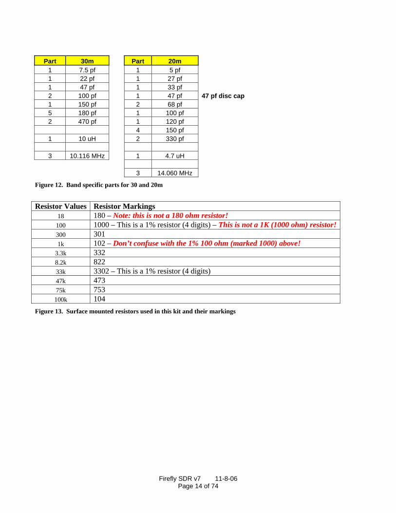
Part 30m Part 20m
1 7.5 pf 1 5 pf 1 22 pf 1 27 pf 1 47 pf 1 33 pf 2 100 pf 1 47 pf 47 pf disc cap 1 150 pf 2 68 pf 5 180 pf 1 100 pf 2 470 pf 1 120 pf 4 150 pf 1 10 uH 2 330 pf 3 10.116 MHz 1 4.7 uH 3 14.060 MHz
Figure 12. Band specific parts for 30 and 20m
Resistor Values Resistor Markings
18 180 – Note: this is not a 180 ohm resistor! 100 1000 – This is a 1% resistor (4 digits) – This is not a 1K (1000 ohm) resistor!300 301 1k 102 – Don’t confuse with the 1% 100 ohm (marked 1000) above!
3.3k 332 8.2k 822 33k 3302 – This is a 1% resistor (4 digits) 47k 473 75k 753 100k 104
Figure 13. Surface mounted resistors used in this kit and their markings
Firefly SDR v7 11-8-06 Page 14 of 74

Figure 14. Close up of part of the surface mounted resistors
Firefly SDR v7 11-8-06 Page 15 of 74

Figure 15. The remainder of the surface mount resistors.
The markings of the surface mounted resistor used in this kit can be confusing. Take special note that “1000” is 100 ohm, 1% resistor (not 1K!) and “180” is an 18 ohm resistor. Also “3302” is a 1% 33K resistor. If in doubt, measure it with an ohm meter! Note: There are a few “one of” surface mounted parts in the color coded parts figure above. It may be good at this time to mount the following single parts just to keep from loosing them: D1 (51v Zener – See PA section), Q5 (FDN335 – See TX Buffer section), C90 (7 pf – see Receiver Front End section)
Firefly SDR v7 11-8-06 Page 16 of 74

Tools and Construction Hints There are many great articles on the web that describe techniques on building surface mount projects. Alas, I am guilty of often using a bit too much solder. Rather than right my own version of this, let me repeat some of these links: www.geocities.com/vk3em/smtguide/websmt.html www.seed-solutions.com/gregordy/Amateur%20Radio/Experimentation/N2PKVNA/SMT.htm www.piclist.com/techref/smds.htm In building this transceiver myself and creating the manual, I have had some problems. These fall into several different categories:
1) IC pins not truly soldered 2) ICs mounted backwards 3) Resistors and capacitors not soldered to the right set of pads 4) Not all parts were installed 5) Bad resistor (part was open)
In helping others, I also had several cases where folks soldered one end of a resistor or capacitor, but not the other end. Between testing prototypes and building the final transceiver, I have built five of the NC2030s and three of the Firefly SDRs. Please learn from my mistakes. Each time an IC is mounted, check the mounting polarity twice before soldering it in. I suggest checking the IC polarity, soldering down one corner pin, and then checking it one more time before finishing the job. I think the old saying is “measure twice, cut once”. I have several times mounted caps and resistors to the wrong set of pads. This problem can be corrected by mounting the resistors first, double checking the resistor placement against the pictures, and mounting the capacitors after all the resistors are mounted. The assembly instructions have been modified to reflect this order. I have once been bit by not mounting all the parts. Double check the pictures against your kit to make sure things end up in the right place. You may find that the components in the pictures may be slightly different from what is in your kit. This may be partially due to the fact that the pictures are of the 20m version. Lastly, I have had IC pins that look soldered, but are not. This happens when the top of the lead of the part gets soldered, but the solder does not extend to the pad. This happened a few times until I figured out a trick to make sure that all pins were properly soldered.
Firefly SDR v7 11-8-06 Page 17 of 74

After soldering pins on both sides to firmly anchor the IC, I run a bead of solder down both sides of the IC. All pins are now shorted to each other. Next I heat of sections of that bead with the soldering iron and use the solder sucker to suck away the excess. You have to be fast removing the iron and getting the sucker in place before the solder has a chance to cool, but this seems to work very well. When using the approach, carefully inspect the pins when finished to make sure there is no solder left between the pins. It is not uncommon for a very light solder film to be left which can be cleaned up with either a knife or a very small screw driver blade or a light touch of the soldering iron. This manual has been set up to build a section, and then test it. The tests are normally quite simple. This should find most problems as we go from stage to stage rather than getting to the end and not knowing where to start. I found building the transceiver over a large cookie sheet eliminated the problem of dropping parts and loosing them. However, when doing the applied voltage tests, you should place a few sheets of clean paper under the boards to keep them from shorting out against the cookie sheet. I find that this radio can be built in about six hours. One good Saturday should do it.
Firefly SDR v7 11-8-06 Page 18 of 74

Bare PC Board Pictures
Figure 16. Top side view of the Firefly SDR PC board
Firefly SDR v7 11-8-06 Page 19 of 74

Figure 17. Bottom side view of the Firefly SDR circuit board.
Firefly SDR v7 11-8-06 Page 20 of 74
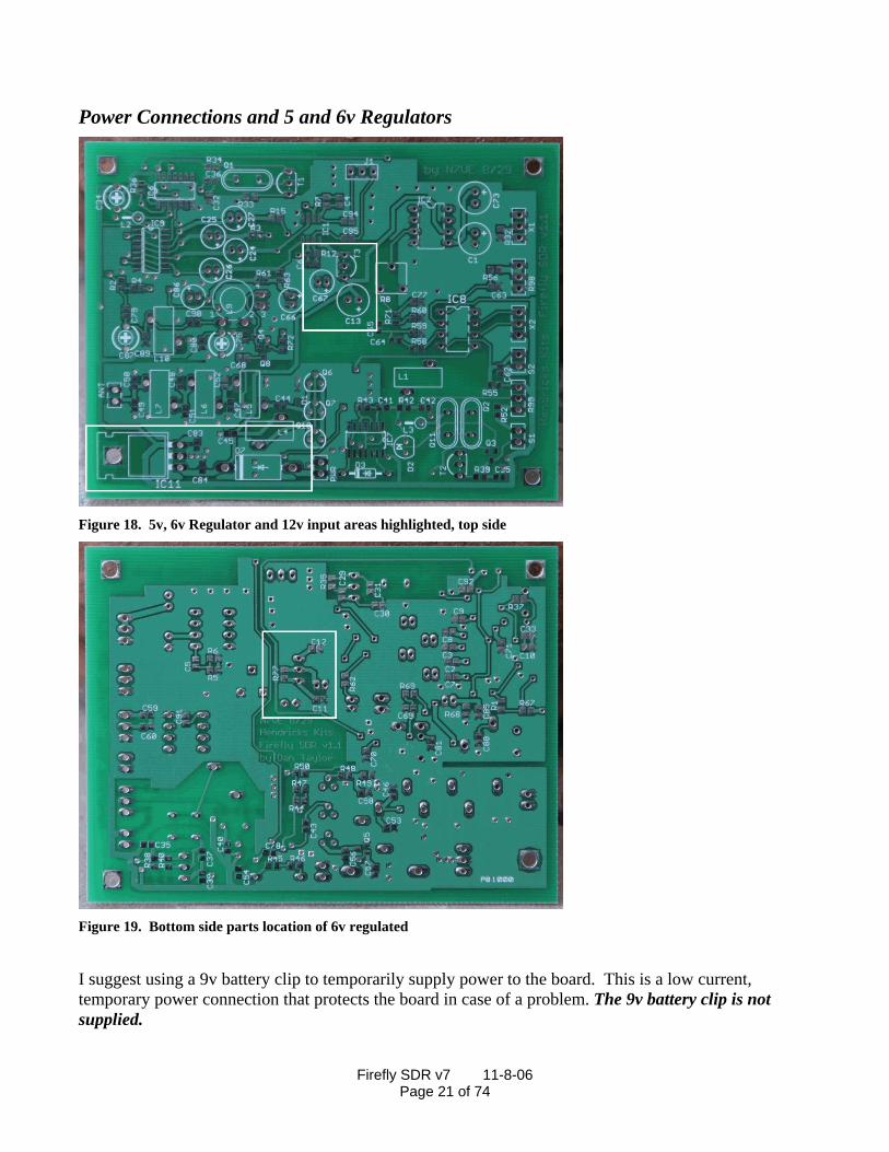
Power Connections and 5 and 6v Regulators
Figure 18. 5v, 6v Regulator and 12v input areas highlighted, top side
Figure 19. Bottom side parts location of 6v regulated
I suggest using a 9v battery clip to temporarily supply power to the board. This is a low current, temporary power connection that protects the board in case of a problem. The 9v battery clip is not supplied.
Firefly SDR v7 11-8-06 Page 21 of 74

Figure 20. Top side view of 5v regulator, protection diode, and 9v temporary connection. Note D7 diode polarization!
Figure 21. Lead forming of the LM78M05 5v regulator before installation
Figure 22. 6v regulator with C67 shorted and C13 installed. Note T3 flat side orientation and C13 stripe orientation.
Figure 23. Bottom side of the 6v regulator w/ C11 and C12 installed
Firefly SDR v7 11-8-06 Page 22 of 74

Install IC11 (LM78M05). Make sure hole of the regulator matches up with the mounting hole on the board! Install T3 (LM78L06), D7 SB320. Double check the polarity against the above picture! Check the diode band polarity, and match the flat side of T3 against the flat side outline on the board. Install 0.1 uf caps (no color markings). Top side: C83, C84; Bottom side: C11, and C12 Install C13, 100uF polarized capacitor. This is a polarized capacitor, so make sure it is installed with the correct polarization. The black stripe on the top of the cap is the negative side of the capacitor. The non-striped side matches with the “+” symbol marked on the board. Double check against the orientation on the board.
Short C67 (not used).
5 and 6v Regulator Tests
Figure 24. Ground point and 5v/6v regulator output test points
Firefly SDR v7 11-8-06 Page 23 of 74

The drain on the 9v battery should be about 9 ma. The current drain can be tested by connecting the 9v battery by one terminal only, then connecting a voltmeter between the remaining battery terminal and remaining 9v battery clip terminal. The input voltage to the board is diode protected. Thus you will not damage the board by hooking the battery up backwards. The tab of the 5v regulator is one of the only good ground connection points on the entire board. All voltage measurements from this point on will this regulator tap as the ground point. Measure and verify the 5v and 6v outputs as shown above. However, if the current drain is right, it is highly likely that all is well. At this time, remove the 9v battery connection.
Sidetone monitor Amplifier
Figure 25. Top side parts location of the CW side tone monitor amplifier
Firefly SDR v7 11-8-06 Page 24 of 74

Figure 26. Bottom side parts location of the CW side tone monitor amplifier
Figure 27. Top side IC2, C73, C1, volume trim pot R8 and R32. Note IC2 polarity and black stripes on C1 and C73.
Firefly SDR v7 11-8-06 Page 25 of 74

Figure 28. Bottom side installation of R5, R6, and C5.
Install the following parts in the following order:
- Install IC2 (LM386-4). Double check the orientation of the IC before soldering it in. Solder one pin, double check the orientation with the picture above, and then solder the rest of the pins.
- Install C1, C73 100 uf. Double check the polarity of the black stripe against the photos
above.
- Install R8 (5K trim resistor), R32 (1K marked 102).
- Install R5, R6 (18 ohm – marked 180) and C5 (0.1 uf – no color code)) on the bottom side.
CW Side Tone Monitor Amplifier Test This will be tested more completely after the next section. The easiest test is to check the board current draw when connected to the 9v battery. At this point the current drain is in the 13.5 to 14.5 ma range.
Firefly SDR v7 11-8-06 Page 26 of 74

Keyer Circuit
Figure 29. Top side location keyer circuitry
Figure 30. Bottom side location of keyer chip components C59, C60, and C91
Firefly SDR v7 11-8-06 Page 27 of 74

Figure 31. Top side keyer parts. Note the orientation of IC8. IC8 Notch is at the top end.
Figure 32. Bottom side components of the keyer circuit
Install IC8 (12F629). Note the IC8 notch orientation in the above picture before soldering! Solder one pin, double check the orientation with the picture above, and then solder the rest of the pins. Install 0.01 uf capacitors (brown color code): Bottom side C59 & C60, top side C62, C63. Install 0.1 uf capacitors (no color code): Bottom side C91, top side C64, C65, C77 Install 3.3K resistors: Top side R59, R60, and R71 (marked 332) Install 1K resistors: Top side R56, R58 (marked 102) Install 8.2K resistors: Top side R55 (marked 822) For temporary testing purposes connect a resistor somewhere in the 10K to 100 K range as shown above across the connections for the CW speed pot R98. I used a 47K resistor because that is what I had closest to hand. This will allow the keyer chip to send “FB” out of the side tone speaker monitor output when the board is powered up.
Firefly SDR v7 11-8-06 Page 28 of 74

Keyer and CW Side Tone Monitor Amplifier Test Connect the 9v battery. If no monitor side tone external speaker is connected, the board current draw when connected to the 9v battery will start at ~ 15.5 ma, then quickly drop back to 14.5 ma. The 1 ma difference is the keyer chip turning on and sending “FB”. The keyer chip will then turn off when done, reducing the current back down to 14.5 ma. A further and more complete test is to connect an external speaker (or set of headphones) to the CW side tone monitor output, X1. The picture below shows a headphone output connected temporarily across X1. R8 is the volume control for this CW side tone output, and the output is quite loud. I suggest turning R8 down a bit to the setting shown below as it is otherwise a bit loud.
Figure 33. Temporary connection of a headphone jack to test the CW side tone monitor speaker output
With a speaker attached, the current drain increased to 24 ma when the board is first powered up and the “FB” is sent. The current then dropped back to 14.5 ma. The high current value will depend on your exact R8 volume setting and the exact impedance of the external speaker. Note: The CW Keyer may not reset properly if the voltage is removed from the rig for only a few seconds. If the chip does not reset properly, it will not send the sign on messages on power up. If you power off the rig and want to power it back on immediately, you may need to press the Keyer push button to make sure the processor burns up all stray charge and thus get reset properly before turning the rig back on. The operating instructions for the keyer are at the end of this manual. The keyer in has several memories, a beacon mode, and a straight key mode where if a straight key is plugged in on power up (or
Firefly SDR v7 11-8-06 Page 29 of 74

if a paddle lever is held on power up), the keyer will disable itself and assume an external straight key is being used. The straight key mode is determined each time the keyer (i.e., the transceiver) is turned on. Disconnect the 9v battery supply.
Receiver Side Local Oscillator
Figure 34. Top side location of the receiver crystal oscillator circuitry
Figure 35. Bottom side location of the receiver crystal oscillator circuitry
Firefly SDR v7 11-8-06 Page 30 of 74

Figure 36. Top side receiver LO parts mounted
Figure 37. Bottom side receiver LO parts mounted
Install 0.1 uf (no color code) capacitors: Bottom side C31 Install 100K resistors: Bottom side R35 (marked 104) Install capacitors: Top side C36 (5 pf – Green/Black) & C32 (47 pf - Red) Install 3.3K resistors: Top side R34 (marked 332) Install 1K resistors: Top side R33 (marked 102) Install 2n4401: Top side T1. Make sure the flat side of T1 matches the flat side silk screen marking on the board. 30m specific parts Bottom side C30 (180 pf - Orange) & C29 (100 pf - Green) Install Q1 10.116 MHz crystal.
Firefly SDR v7 11-8-06 Page 31 of 74

20m specific parts Bottom side C30 (150 pf - Yellow) & C29 (68 pf – Blue/Black) Install Q1 14.060 MHz crystal.
Receiver Side Local Oscillator Test Connect the 9v battery. After the keyer finishes sending “FB”, the board current draw when connected to the 9v battery will be in the 15.8 to 14.8 ma range, about 1 ma higher than in the previous current test. A second test is to listen for the oscillator at either 10.114 (30m) or 14.060 MHz (20) on another receiver. Disconnect the 9v battery supply.
90 Degree Phasing Section and LO Buffer
Figure 38. Top side location of the receiver crystal oscillator circuitry
Firefly SDR v7 11-8-06 Page 32 of 74

Figure 39. Bottom side location of the receiver crystal oscillator circuitry
Figure 40. Top side receiver LO parts mounted
Figure 41. Bottom side receiver LO parts mounted
Firefly SDR v7 11-8-06 Page 33 of 74

Install IC6 (74AHC04): Top side. Caution! Install with the polarity as shown above! Solder one pin, double check the orientation with the picture above, and then solder the rest of the pins. Install capacitor: Top side C34, 50 pf trim cap. Caution! Install flat side down as shown above! These caps must have the right orientation or it will affect tune up (hot end, ground end). See the figures above! Install resistor: Top side R36, 100K (marked 104) Install capacitors: Bottom side C92 (0.1 uf – No color code) Install 1K resistor: Bottom side R37 (marked 102) 30m specific parts Bottom side - C33 (22 pf – Red/Black) Top side - L2, 10 uH molded choke. Note the part is installed standing on end. 20m specific parts Bottom side - C33 (27 pf – Red/Green) Top side - L2, 4.7 uH molded choke. Note the part is installed standing on end.
90 Degree Phasing Section and LO Buffer Tests Connect the 9v battery. After the keyer finishes sending “FB”, the board current draw when connected to the 9v battery will be in the 22 ma range. Disconnect the 9v battery supply.
Detector Circuit
Figure 42. Top side location of the detector circuit
Firefly SDR v7 11-8-06 Page 34 of 74

Figure 43. Bottom side location of the detector circuit
Figure 44. Top side Detector, R2, R4, C86, and IC9
Figure 45. Close up of bottom side detector circuit
Firefly SDR v7 11-8-06 Page 35 of 74

Install IC9 (74CBT3253): Top side. Caution! Install with the polarity as shown above! Solder one pin, double check the orientation with the picture above, and then solder the rest of the pins. Install capacitor: Top side C86, 22 uf. Caution! Install with black stripe as shown above! Install shorting strips: Top side C24, C25, C26, and C27. Install “U” formed wires to short out these unused caps as shown above. Install resistors: Top side R4 (18 ohms – marked 180), R2 (300 ohms - marked 301) Install 0.1 uf (no color code) capacitors: Bottom side C71, C85 Install 0.01 uf (Brown) capacitors: Bottom side C2, C3, C7, C8 Install resistors: Bottom side R1 (300 ohm – marked 301), R67 & R68 (3.3K – marked 332)
Detector Circuit Tests Connect the 9v battery. After the keyer finishes sending “FB”, the board current draw when connected to the 9v battery will be in the 27 to 29 ma range. Measure the voltage at either end of R4. Again, the ground reference for this test is the tab of the large 78M05 voltage regulator. The measured voltage should be in the 2.2 to 2.5v range. This test makes sure that the input voltage divider works. Measure the voltage on the shorting strap of unused capacitors C24, C25, C26, and C27. If the detector is running correctly, the voltage at each of these points should be the same as seen across R4 above, 2.2 to 2.5v. Disconnect the 9v battery supply.
Firefly SDR v7 11-8-06 Page 36 of 74

Receiver Audio Preamp
Figure 46. Top placement of receiver audio preamp stage
Figure 47. Close up of the parts in the audio preamp stage (top side only)
Install IC1 (LT6231): Top side. Caution! Install with the polarity as shown above! Solder one pin, double check the orientation with the picture above, and then solder the rest of the pins. Install capacitors: Top side C4, C6 (150 pf - Yellow) Use the right pads! See the figure above! Install capacitors: Top side C94, C95 (0.1 uf – no color code) Install resistors: Top side R3, R15 (100 ohms – 1% resistor marked 1000) Install resistors: Top side R7, R12 (33k ohm – 1% resistor marked 3302)
Firefly SDR v7 11-8-06 Page 37 of 74

Receiver Audio Preamp Tests Connect the 9v battery. After the keyer finishes sending “FB”, the board current draw when connected to the 9v battery will be in the 33 to 35 ma range. Measure the voltage at the IC1 end of C94 and C95. Again, the ground reference for this test is the tab of the large 78M05 voltage regulator. The measured voltage should be somewhere mid-range in the 0 to 5v range, perhaps as low as 1.5v and as high as 3.5v. The voltage should be closer to 2.2 to 2.5v after the receiver opposite sideband suppression is tuned up during the alignment section. The voltage should not be 0v or 5v on the IC1 end of C94 or C95. Note that the DC voltage out of the pre-amp will shift based upon the tuning setting of the detector clock phasing network, C34 (upper right hand corner). If you have concerns on the op-amp output voltage, adjust this trip cap and watch the DC output shift around. This is the receiver picking up its own local oscillator signal as a DC offset voltage. Disconnect the 9v battery supply.
Receiver Front End and T/R Switch
Figure 48. Top placement of receiver front end and T/R switch
Firefly SDR v7 11-8-06 Page 38 of 74
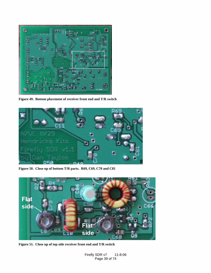
Figure 49. Bottom placement of receiver front end and T/R switch
Figure 50. Close up of bottom T/R parts. R69, C69, C70 and C81
Figure 51. Close up of top side receiver front end and T/R switch
Firefly SDR v7 11-8-06 Page 39 of 74

Install Q4 and Q8 (BSS123 – Blue in black package): Top side. Install capacitors: Top side C68 (0.1 uf – no color code) Install resistor: Top side R72 (3.3K – marked 332) Install trimmer caps: Top Side C87, C75 50 pf trim cap. Caution! Install flat side of trim caps as shown. These caps must have the right orientation or it will affect tune up (flat side hot end, rounded ground end). See “Figure 40. Top side receiver LO parts mounted “ for an alternate style trim cap that may be in your kit..
Figure 52. Close up of input receiver filter inductor L9. 30m values shown. For other bands see text.
The wire used in this kit is especially designed to be easy to strip using heat. Place some excess solder on the tip of your soldering iron (“solder blob”). Place the end of the cut wire into the blob, and the insulation will burn off. Work the iron down the wire to strip off as much insulation as needed, refreshing the solder blob as needed. Install capacitors: Bottom side C69 & C70 (0.01 uf - Brown) Install resistor: Bottom side R69 (3.3K – marked 332) 30m specific parts Bottom side – C81 (180 pf – Orange) Top side - C79 (47 pf - Red), C89 (150 pf - Yellow), C90 (7.5 pf – Orange/Black) Top side - Install L9 - T37-6 yellow core, 19T # 26 primary, 4T #32 secondary. Use 10” of #26 wire (the larger diameter wire supplied in the kit) for the primary, 4” of #32 (the very fine diameter wire supplied) for the secondary.
Firefly SDR v7 11-8-06 Page 40 of 74

Top side - Install L10 - T37-6 yellow core, 18T # 26. Use 10” of #26 wire (the larger diameter wire supplied in the kit) for the primary. 20m specific parts Bottom side – C81 (120 pf – Yellow/Black) Top side - C79 (33 pf – Red/Blue), C89 (100 pf - Green), C90 (5 pf – Green/Black) Top side - Install L9 - T37-6 yellow core, 15T # 26 primary, 3T #32 secondary. Use 10” of #26 wire (the larger diameter wire supplied in the kit) for the primary, 4” of #32 (the very fine diameter wire supplied) for the secondary. Top side -Install L10 - T37-6 yellow core, 15T # 26. Use 10” of #26 wire (the larger diameter wire supplied in the kit) for the primary.
Receiver Front End and T/R Tests Connect the 9v battery. After the keyer finishes sending “FB”, the board current draw when connected to the 9v battery will be in the 33 to 35 ma range. The current drain should not have changed from the current drain measured in the previous section. .There is not much that can be tested in this stage at this point. The drivers for the T/R switching transistors will not be installed until later. In past projects, there have been a lot of problems with the enamel wire on the inductors not being properly stripped before the inductors are installed. One simple test is to place an ohm meter across the PC board pads of L9 (two pads) and L10 (four pads) to ground (the tab of the 5v regulator) to make sure the inductor leads had been properly stripped and installed. Disconnect the 9v battery supply.
Firefly SDR v7 11-8-06 Page 41 of 74

Transmitter VXO
Figure 53. Top side location of the transmitter VXO
Figure 54. Bottom side location of the transmitter VXO
Firefly SDR v7 11-8-06 Page 42 of 74

Figure 55. Close up of top side installed transmitter VXO parts
Install transistors: Top side. T2 (2N4401), Q3 (BSS123 – Blue in black package) Caution! Install with the polarity as shown above! The flat side of T2 matches the flat side on the silkscreen outline. Install capacitors: Top side C55 & C42 (0.1 uf – no color code). Install resistors: Top side R39 & R52 (1K – marked 102), R42 (100K – marked 104) Install varicap tuning diode: Top side D2 (MV209). Caution! Install with the polarity as shown above! The flat side of D2 matches the flat side on the silkscreen outline.
Figure 56. Close up of the bottom side installed transmitter VXO parts
Install capacitors: Bottom side C35 (0.1 uf – No color code), C40 (22 pf – Red/Black) Install resistors: Bottom side R40 (100K ohm – marked 104), R38 (3.3K – marked 332)
Firefly SDR v7 11-8-06 Page 43 of 74

30m specific parts Bottom side – Install capacitors: C37 (100 pf - Green), C38 (180 pf - Orange) Install crystals: Top side Q2, Q11 (10.116 MHz) Install inductor: Top side L1 - T37-6 yellow core, 56T #32. Use the #32 wire (the very fine diameter wire supplied). 20m specific parts Bottom side – Install capacitors: C37 (68 pf – Blue/Black), C38 (150 pf - Yellow) Install crystals: Top side Q2, Q11 (14.060 MHz) Install inductor: Top side L1 - T37-6 yellow core, 40T #32. Use the #32 wire (the very fine diameter wire supplied). Note: L1 needs to be coated with clear fingernail polish to both seal the windings to the core and seal the core to the board. Not all clear fingernail polishes dry hard. My wife recommends Sally Hansen Diamond Strength (source: Ulta). It seems to work very well. Sealing windings to the core improves the temperature stability of this oscillator.
Transmitter VXO Tests Connect the 9v battery. After the keyer finishes sending “FB”, the board current draw when connected to the 9v battery will be in the 33 to 35 ma range. The current drain should not have changed from the current drain measured in the previous section. Shorting S1 (TX VXO spot switch) should see the current drain increase by another 1 ma. At this point in time, there will be no voltage across D2, the varactor tuning diode, so the VXO will be tuned to a very low frequency. Thus you can verify that the VXO is oscillating by listening for the transmit VXO as the jumper header S1 is shorted. The VXO frequency might end up being lower than 10.1 MHz (30m version only) Disconnect the 9v battery supply.
Firefly SDR v7 11-8-06 Page 44 of 74

Transmitter Buffer Circuit
Figure 57. Top side location of the TX Buffer circuit
Figure 58. Bottom side location of the TX buffer circuit.
Firefly SDR v7 11-8-06 Page 45 of 74

Figure 59. Top side TX buffer parts installed. IC7, D3, R43, C41
Figure 60. Bottom side TX buffer with parts installed
Install IC: Top side. IC7 (74AC00) Caution! Install with the polarity as shown above! Solder one pin, double check the orientation with the picture above, and then solder the rest of the pins. Install capacitor: Top side C41 (5 pf – Green/Black). Install resistor: Top side R43 (100K – marked 104) Install diode: Top side D3 (1N4148) Install capacitors: Bottom side C54, C78, C43, C56, C57 (0.1 uf – no color code) Install capacitors: Bottom side C58 (0.01 uf - Brown)
Firefly SDR v7 11-8-06 Page 46 of 74

Install resistors: Bottom side R45, R46, R44, R47, R49 (75K ohm – marked 753) Install resistors: Bottom side R50 (47K ohm – marked 473), R48 (8.2K ohm – marked 822) Install transistor: Bottom side Q5 (FDN335 – Red in Black package)
Transmitter Buffer and T/R Switch Tests Connect the 9v battery. After the keyer finishes sending “FB”, the board current draw when connected to the 9v battery will be in the 33 to 35 ma range. The buffer stage draws basically no additional current when not transmitting. At this point, the drivers for the T/R switch have been put into place so that the T/R switch can now be tested. Refer to the figure below:
Figure 61. Top side test points for the T/R switch in the receiver front end
With the board powered up in receive mode, point A should be 5v, and point B should be 0v or at least less than 1v. When in transmit mode, these readings should flip: point A 1v or less and point B at 5v. The T/R transition can be tested by shorting the keyer paddle inputs as shown in the diagram below:
Firefly SDR v7 11-8-06 Page 47 of 74

Figure 62. Location of keyer paddle inputs to test the T/R switch
I typically use my pointed tweezers to temporarily short the paddle inputs for a quick test. Disconnect the 9v battery supply.
Transmitter PA Circuit
Figure 63. Top side view of the PA circuit
Firefly SDR v7 11-8-06 Page 48 of 74

Figure 64. Bottom side view of the PA circuit
Figure 65. Top side parts view of the PA circuit. C50 (left top end cap) not used on the 30m version.
Figure 66. Bottom side part view of PA circuit. C53 not used in the 30m version
Install diode: Top side D1 (51v Zener Diode – No color code. Single item in black package). See figure below! Double check band orientation!
Firefly SDR v7 11-8-06 Page 49 of 74

Figure 67. Close up of Zener diode D1 with band orientation
Install transistors: Top side Q6, Q7, and Q10 (BS170). Double check flat side transistor orientation in above figures! Install capacitor: Top side C44, C45 (0.1 uf – No color) 30m specific parts Install capacitor: Top side C47 & C48 (470 pf - Blue), C49 (180 pf - Orange) Install capacitors: Bottom side C46 (180 pf - Orange) Note: make sure the windings on the following inductor are evenly spaced over the entire core! Install inductors: Top Side L5 & L7 - T37-6 (yellow core) 16T #26 - 10” of wire Install inductors: Top Side L6 - T37-6 (yellow core) 18T #26 - 10” of wire Install inductors: Top Side L4 - FT37-43 (dark core) 10T #26 - 10” of wire
Firefly SDR v7 11-8-06 Page 50 of 74

Figure 68. Location of 20m modification, C14. Bottom side of TX low pass filter L6.
20m specific parts Install capacitor: Top side C47 & C48 (330 pf – Red/Yellow), C49 (150 pf - Yellow) Install capacitors: Bottom side C46 (150 pf - Yellow), C14 (47 pf disc cap – see figure above) Note: make sure the windings on the following inductor are evenly spaced over the entire core! Install inductors: Top Side L5 & L7 - T37-6 (yellow core) 13T #26 - 10” of wire Install inductors: Top Side L6 - T37-6 (yellow core) 14T #26 - 10” of wire Install inductors: Top Side L4 - FT37-43 (dark core) 8T #26 - 10” of wire Note: The use of C14 on 20m seems to have boosted the output power from 2.5 to 3.5w.
Transmitter PA Tests Connect the 9v battery. After the keyer finishes sending “FB”, the board current draw when connected to the 9v battery will be in the 33 to 35 ma range.
Figure 69. Antenna coax connection to transceiver. Upper connection is ground, lower is antenna.
Connect a coax to the board and connect the transceiver to a 50 ohm load. Switch the 9v battery for a more stout 12v power source. Keying the transmitter as in the previous section should produce a 2.5w output.
Firefly SDR v7 11-8-06 Page 51 of 74

Board Connections
Figure 70. Connections for J1, I/Q (R/L) audio output to the PC sound card input
Figure 71. Connections of the I/Q audio output to its audio jack
Firefly SDR v7 11-8-06 Page 52 of 74

Figure 72. Connections for X1 and R98, CW side tone monitor speaker and 100K CW speed pot.
Figure 73. Connections to CW mon speaker jack, CW speed pot. Remove temporary resistor across R98.
Firefly SDR v7 11-8-06 Page 53 of 74

Figure 74. Connections for keyer paddle inputs (X2) and for keyer programming push button switch (S2)
Figure 75. Visualization of paddle jack and keyer programming switch connections
Figure 76. Connections for TX spot switch (S1) and TX VXO 10K tuning pot (R99).
Firefly SDR v7 11-8-06 Page 54 of 74

Figure 77. Visualization of TX tuning pot and VXO spot switch connections. Switch shown “Spot On”.
Figure 78. Connections for 12v to the board
Figure 79. Antenna Connections
Firefly SDR v7 11-8-06 Page 55 of 74

System Connection Block Diagram
Figure 80. External connections from a case view
Figure 81. Diagram of the major external interfaces of the Firefly SDR, less front panel controls.
Firefly SDR v7 11-8-06 Page 56 of 74
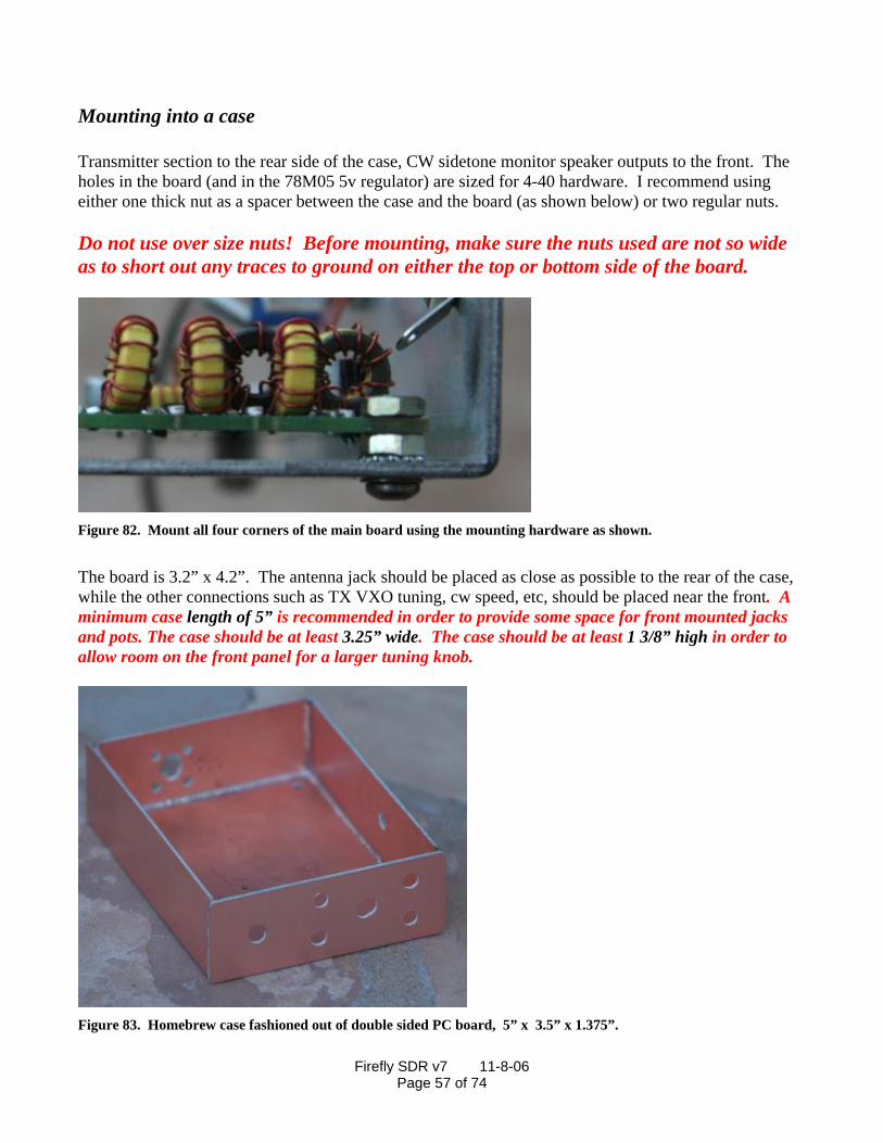
Mounting into a case Transmitter section to the rear side of the case, CW sidetone monitor speaker outputs to the front. The holes in the board (and in the 78M05 5v regulator) are sized for 4-40 hardware. I recommend using either one thick nut as a spacer between the case and the board (as shown below) or two regular nuts. Do not use over size nuts! Before mounting, make sure the nuts used are not so wide as to short out any traces to ground on either the top or bottom side of the board.
Figure 82. Mount all four corners of the main board using the mounting hardware as shown.
The board is 3.2” x 4.2”. The antenna jack should be placed as close as possible to the rear of the case, while the other connections such as TX VXO tuning, cw speed, etc, should be placed near the front. A minimum case length of 5” is recommended in order to provide some space for front mounted jacks and pots. The case should be at least 3.25” wide. The case should be at least 1 3/8” high in order to allow room on the front panel for a larger tuning knob.
Figure 83. Homebrew case fashioned out of double sided PC board, 5” x 3.5” x 1.375”.
Firefly SDR v7 11-8-06 Page 57 of 74

A Note on PC Sound Cards The SDR receiver front end puts out very low level audio signals in the 0 to 24 KHz range that is converted into digital form by the sound card of a computer. It is good to keep in mind that the sensitivity of the SDR receiver relates directly to the performance of the sound card A/D converter. Generic PC sound cards use 16 bit A/D converters. All A/D converters have a maximum input voltage of around 2 to 5v. The performance of 16 bit converters are typically roughly 80 db of dynamic range. Pro sound cards use 24 bit converters which are in the 98 to 122 db. The currently affordable high end 24 bit cards are in the 108 to 112 db of dynamic range, which is 30 db more sensitivity than the 16 bit card. The very high end 122 db A/D parts currently exist, are being designed into a sound card that should be available in a few months by the HPSDR group and TAPR. The point of all of this is that the large signal dynamic range and the receiver sensitivity is a function of the quality of the A/D converters. The 16 bit sound card in most PCs will not allow the full receiver performance to be realized. However, it will allow the user to get on the air, make contacts, and give SDR receivers a trial spin before moving on to a better sound card. The current higher end sound cards are the Delta-44 ($150, designed for a desktop PC) and the Edirol FA-66 ($350, designed for a firewire interface to a laptop). Flex Radio carries these sound cards: http://www.flex-radio.com/ It needs to be noted that most laptops are reported not to have stereo sound card inputs, but rather mono inputs. If the receiver is connected to a mono input, the SDR software will work, but will be unable to determine the difference between a signal 1 KHz higher from the center 10.114 MHz from that 1 KHz lower than 10.114 MHz. Thus signals that appear at 10.108 MHz (10.114 – 6 KHz) could really be a signal at 10.120 MHz (10.114 + 6 KHz). The use of the both the I/Q outputs from the receiver allows the SDR software to determine which side of 10.114 MHz the signal belongs to and to null the image.
Pre-Loading of SDR software on the PC In order to tune up the receiver, the I/Q audio output must be connected to the sound card input of a PC and a SDR software package must be installed and verified. There are several SDR software packages that are very popular, “Rocky” and “PowerSDR”. Both are free and are available on line. Of the two, I think that PowerSDR that has seen the most development activity, and is what I recommend. Remember that since the vast majority of the receiver functionality is in software, improvements to SDR software is like getting receiver hardware upgrade for free. For example, PowerSDR just release a beta version that allows two receivers to be run at the same time, one in the right speaker, the other in the left. This allows one to listen to both sides of a DX pile up when operating a split, or allows to monitor a station you want to work while you tune around elsewhere in the band.
Firefly SDR v7 11-8-06 Page 58 of 74

Both Rocky and PowerSDR are set up to work with softrock receiver. The receiver portion of this rig is softrock compatible. Any SDR software that can run a softrock receiver can be used for the receiver side of the Firefly SDR. Rocky: http://www.dxatlas.com/rocky/ This page for Rocky gives the setup instructions for the Rocky software package. PowerSDR: http://www.flex-radio.com/testdrive.htm This gives a link for you to get the PowerSDR software up and running on your computer. If you have any question on whether or not your computer is fast enough to run SDR software, I would suggest running this and checking the CPU meter on your computer. One of the features of both Rocky and PowerSDR is that it allows you to run a prerecorded sound file. Note that playing a prerecorded sound file exercises the full receiver functionality since the receiver cannot tell the difference between sound samples from the sound card from sound samples played from a file. If the sound samples work, your computer will work. http://www.flex-radio.com/downloads.htm#PowerSDR This link includes one sound file. Use this for a test drive of both Rocky and PowerSDR. There is no reason why you cannot install both packages on your computer and try them both out. The computer requirements vary widely from computer to computer. In general, any computer with a video on the mother board will have much worse performance than a computer with dedicated video card. It is much cheaper for a computer manufacturer to use an integrated video chip set on the motherboard (almost all laptops are this way, as well as the low end desktops), but the video memory, which is used all the time for refreshing the display, is shared with the computer, thus the computer runs slow compared to the same computer with a dedicated video card. The suggestions that I have seen recommend at least a 1 GHz PC. This should get you going for the standard +/- 24 KHz (48 kbps sampling rate) receiver reception range. There are sound cards available that also support 96 Kbps sampling (+/- 48 KHz receiver tuning range) and even 192 Kbps (+/- 96 KHz receiver tuning range). Flex Radio recommends a 3 GHz PC when sampling at 192 Kbps. Keep in mind that the +/- 24 KHz tuning range of the receiver exceeds the tuning range of the VXO transmitter, so this does not really concern this kit. However, if you are looking to get a new computer, the 3 GHz rate would be one to keep in mind.
Firefly SDR v7 11-8-06 Page 59 of 74

Notes on loading PowerSDR
Figure 84. Select the setup tab to get to this window. Select SoftRock, and set the center frequency.
The nominal center frequencies are 10.114, 14.058, or 18.095 MHz. If you are using a signal source of a known signal level (like the KX1/KX2 generators), select the calibration tab above.
Figure 85. Sheet used to calibrate the signal strength readings in Power SDR
Firefly SDR v7 11-8-06 Page 60 of 74

Enter the frequency of the test signal, its input signal strength, then click start.
Figure 86. DSP/Image Reject tab used to null opposite sideband signal
This is the tab that is used to fine tune the image rejection response. Course tune using the sliders, then fine tune with the up arrow/down arrow on the box. Ideally, the rejection should be nulled using a signal ~ 5 KHz lower than the center frequency (10.114, 14.058, 18.095 MHz).
Figure 87. Generic settings – NB on, 500 Hz filter, CWU, proper band selected (30m here)
Firefly SDR v7 11-8-06 Page 61 of 74

The most important point here is to click on “NB” to enable the noise blanker. Also note that the receiver will not turn on until the “Standby” button in the upper left is clicked (off as shown).
SDR Receiver Resources If you have problems with the above packages, there are two user groups that have very knowledgeable folks that can probably help. http://groups.yahoo.com/group/softrock40/ This is the softrock receiver group. Since the receiver used here looks like a softrock receiver (i.e., I/Q audio into a sound card), this group is a very good resource for hardware and software issue. http://mail.flex-radio.biz/pipermail/flexradio_flex-radio.biz/ This is the group for the PowerSDR software. If you use this package, you should probably monitor this group for software upgrades. Although this group is primarily focused on the Flex Radio SDR-1000, since their software is compatible with the softrock, it is also compatible with the receiver side of the Firefly SDR.
Firefly SDR v7 11-8-06 Page 62 of 74

Receiver Tune Up
Figure 88. Adjustment points for tuning up the receiver.
The adjustment is very straight forward. First a strong, steady signal source is required. Some examples of signal sources are:
- A RF signal generator. For this purpose, a setting of –50 dbm is ideal. - A crystal oscillator loosely coupled into the front end (1 to 2 pf in series). QRP crystals are
available from a number of sources including Norcal. - A marker generator such as the one available from Norcal. - A QRP transmitter transmitting at minimum power into a dummy load produced a very strong
signal that can be readily picked up using a 1 inch “sniffer” stub of wire connected to the antenna port of the NC2030. DO NOT TRANSMIT DIRECTLY INTO THE FRONT END OF THE RECEIVER!
- Over the air signals can be used, but these are usually neither strong nor consistent. The first step is to peak the receiver preselector trim pots. With the receiver connected to the PC and with the SDR sound card connected, the receiver center frequency is roughly 10.114 MHz. This center frequency can be applied to the set up portion of the SDR software.
Firefly SDR v7 11-8-06 Page 63 of 74

With one of the above signals applied to the input, the receiver Preselector trim caps are adjusted for best received signal strength. Alternating back and forth between the two caps quickly peaks the receiver front end. The next step is to look at the tune up signal and its mirror image on the far side of 10.114 MHz. For example, if the target signal is 10.110 MHz, there will be an image of this signal at 10.118 MHz. First check to see which signal is smaller. There should be some small opposite sideband suppression at this point. If the 10.110 signal is larger, all is well. If on the other hand if the signal at 10.118 MHz is larger, then the I and the Q signals are backwards and need to be reversed. If all is well, the opposite sideband image should be nulled out as much as possible using phase adjustment trimmer cap as shown above. When it is nulled out as much as can be done, the remainder of the nulling must be done in software. Rocky is especially good at this as it automatically starts to try to null out images of strong signals. I like PowerSDR better, but there are amplitude and phase adjustments that allow the signal to be nulled out to nothing. I suggest reading the PowerSDR manual to find out how to set up the software to run in a “softrock” compatible mode, how to set the softrock fixed frequency, and how to calibrate the signal strength when using a calibrated signal source such as the XG1 and XG2 from Elecraft.
Operating the Firefly SDR I am not sure what to say here. There is a manual on the Flex Radio web site that describes how to tune using the SDR software. First I suggest practicing tuning in signals on the band. My favorite two tuning modes are point and click & drag and drop. Using point and click, placing the cursor in the spectrum window and right clicking on the mouse will turn on cross hairs. Right clicking will toggle this cross hair mode on and off. With the cross hairs on, left clicking on a signal will place it in the middle of the receiver passband. With drag and drop, you can use the left mouse button to “drag” a signal into the middle of the receiver passband. When you get to the point of wanting to answer a signal on the air, turn the “spot” switch on and you will be able to see the transmit signal as you turn the TX tune knob. Tune the TX spot signal and you will be able to visually place it right on top of the signal you are listening to. At that point, the transmitter is set up and ready to go. Turn off the TX spot switch and use the keyer paddles to communicate with the other end. The monitor speaker output provides up to 1w of audio power. Thus, an amplified speaker is not needed. The on board 5K trimmer resistor (R8) in the keyer/cw sidetone monitor amplifier section is the volume control for the output level of this output. Set the volume to a comfortable level. There is no transmit connection into the SDR software, so the SDR receiver is still “on” during transmit even though the actual receiver hardware is turned off during transmit. Thus the SDR receiver produces anomalous audio output during transmit, it sounds kind of like a “thump”, so the CW sidetone output on the separate side tone monitor speaker is used to overcome the noise of the SDR receiver during the transmit period.
Firefly SDR v7 11-8-06 Page 64 of 74

Note that you have two speaker outputs, one set from the PC that carries the SDR receiver output, and a separate speaker output for cw side tone. The Firefly SDR has a built in keyer, complete with a memory function. The instruction on using the keyer and all of its functions are at the end of this document. If you never want to bother with the memory functions, or the beacon mode, or changing the keyer side tone frequency, just plug in a paddle and go. The only thing you really need to know is how to use the cw speed control on the front panel. The keyer has a straight key mode where a straight key (or an external keyer) can be plugged into the transceiver. When the transceiver is turned on, the keyer chip looks to see if one side of the paddle is grounded (like what would happen with a mono straight key plug), and the keyer will enter straight key mode. If you want to use paddles again, simple power off the rig and turn it on again to clear out straight key mode. The keyer also has a handy “tune” mode. Hold both the dot and dash paddles closed for five alternating dots and dashes and the transmitter will go into a steady transmit. Pressing either paddle will cancel the tune mode. Read the keyer operating section. There are lots of neat things that this keyer can do.
Firefly SDR Customizations and Optimizations The gain of the audio pre-amplifiers is currently set by the resistors R7 and R12 (33K). The input impedence is essentially 300 ohms, so the gain of the op-amp is 33000/300 = 110x. In addition, the fact that the op-amp is operated in a differential mode, thus there is a hidden additional 2x gain for a total of 220x. This translates to a db gain of 20*log10(220) = 46.8 db. This amount of gain was used in order to maximize the sensitivity of the receiver. As it is, the noise floor of my Presonus Firebox increases by only 2 db as I power up the receiver. The current 3 db rise, 500 Hz sensitivity is around -127 to -128 dbm when measured using the Firebox “sound card”. However, on 30m this sensitivity level is excessive. The SDR software measures the 20m background noise at about -100 dbm at my suburban location. From a receiver performance perspective, it is good to have the receiver noise floor 10 to 15 db lower than the band noise. Thus, for my and my band conditions at my location using my 500 ft loop antenna, I have roughly 12 db too much gain in my receiver front end. This excess gain will vary significantly from sound card to sound card. Thus, for your sound card, the background noise of the receiver in a 500 Hz bandwidth can be measured with the receiver connected to a 50 ohm dummy load. This noise level can be compared to the band noise on 30m under good band conditions to see the difference. If your sound card is less sensitive, and the difference is less than 15 db, there is no reason to change anything.
Firefly SDR v7 11-8-06 Page 65 of 74

However, if like me, you see a difference significantly larger than 15 db, it may be worth while to reduce the gain of the receiver. The very best way to do this is not to reduce the gain of the receiver op-amp by reducing the 33K feedback resistors. The best way is to change the attenuator in the front end of the receiver. This affects resistors R1 & R2 (300 ohms) and R4 (18 ohms). The input attenuator is currently 3 db. Increasing this attenuation (rather than reducing the op-amp gain) will not only reduce the signal out of the op-amp, but will also reduce the signal at the detector, making it behave better, and also reduce the signal at the input to the op-amp, helping it behave better. In addition, the extra attenuation will serve to further decouple the receiver pre-selector filter from the detector input, allowing for a flatter, more uniform wideband image rejection response. Thus changing the input attenuator to the receiver is the preferred means of reducing overall receiver gain than reducing the op-amp gain. Below is a list of resistor values for different attenuator values: Attenuation R1 & R2 R4 Rx Attenuation R1 & R2 R4 Rx
3 300 18 - 9 107 63 166 4 220 24 825 10 98 72 145 5 182 31 462 15 73 139 96 6 153 38 312 20 62 252 78 7 133 46 239 25 57 452 70 8 118 54 194 30 54 805 66
Figure 89. Pi Attenuator values – 3 db to 30 db
If you want to change to a higher value of attenuator, R2 and R4 can be readily replaced since they are on the top side. However, R1 is on the bottom side of the board. Rather than remove R1, the value of Rx can be applied instead to the top side as shown in the figure below:
Figure 90. If the input attenuator is increased, Rx can be placed across the above 2 points, keeping R1 as is.
Firefly SDR v7 11-8-06 Page 66 of 74

In order to get exactly the attenuation desired, the resistors are very odd values. However, there is no real gain to being so precise. I suggested using the 5% value that is closest to that listed above. This will be good enough. There are two other customizations that can be done. First, the tuning range is fairly non-linear. The tuning range can be made more linear by adding a 4.7K resistor across the VXO tuning pot (R99) as shown below:
Figure 91. Tx VXO tuning linearity improved by using an external 4.7K resistor
The second customization is to add a small 5k trim pot to one end of R99 is the bottom end of the tuning range goes below 10.100 MHz with your crystals. In my v1.0 board, the bottom end of the tuning range was 10.092 KHz. The v1.1 board bottom end range was 10.102 MHz. This difference in tuning range is primarily due to the differences in crystals between the two boards. If the bottom end of the tuning range is significantly below 10.100 MHz, then it would be advantageous to add a small trim pot between R52 and its connection to R99, the TX VXO tuning pot. This trim pot can then be adjusted so that the bottom end of the TX VXO stops at 10.100 MHz with the spot switch turned on. This will allow the entire tuning range of R99 to tune useful coverage range, making the TX VXO easier to tune. One more modification: The power output on 30m can be raised from 2.5w to 3.5w by adding a 47 pf disc cap at the C14 location as shown in the PA section above. This both increases the power and reduces the second harmonic.
Firefly SDR v7 11-8-06 Page 67 of 74

Appendix A. Parts List Part Value Package Part Value Package C1 100 uf E-025X065 IC1 LT6231 SO08 C2 0.01 uf C0805 IC2 LM386-N4 LM386 C3 0.01 uf C0805 T3 78L06 78LXX C4 150 pf C0805 IC6 74AHC04D SO14 C5 0.1 uf C0805 IC7 74AC00D SO14 C6 150 pf C0805 IC8 12F629 DIL8 C7 0.01 uf C0805 IC9 74CBT3253D SO16 C8 0.01 uf C0805 IC11 7805T TO220H C9 0 pf C0805 C10 0 pf C0805 Q3 BSS123 SOT23 C11 0.1 uf C0805 Q4 BSS123 SOT23 C12 0.1 uf C0805 Q5 FDN335 SOT23 C13 100 uf E-025X065 Q6 BS170 SOT54E C31 0.1 uf C0805 Q7 BS170 SOT54E C32 47 pf C0805 Q8 BSS123 SOT23 C34 50 pf trim cap Q10 BS170 SOT54E C35 0.1 uf C0805 C36 5 pf C0805 R1 300 M0805 C40 22 pf C0805 R2 300 M0805 C41 5 pf C0805 R3 100 M0805 C42 0.1 uf C0805 R4 18 M0805 C43 0.1 uf C0805 R5 18 M0805 C44 0.1 uf C0805 R6 18 M0805 C45 0.1 uf C0805 R7 33k M0805 C50 0 pf C0805 R8 5K trim pot 3318_TRIMMER C51 0 pf C0805 R12 33k M0805 C52 0 pf C0805 R15 100 M0805 C53 0 pf C0805 R32 1k M0805 C54 0.1 uf C0805 R33 1k M0805 C55 0.1 uf C0805 R34 3.3k M0805 C56 0.1 uf C0805 R35 100k M0805 C57 0.1 uf C0805 R36 100k M0805 C58 0.01 uf C0805 R37 1k M0805 C59 0.01 uf C0805 R38 3.3k M0805 C60 0.01 uf C0805 R39 1k M0805 C62 0.01 uf C0805 R40 100k M0805 C63 0.01 uf C0805 R42 100k M0805 C64 0.1 uf C0805 R43 100k M0805 C65 0.1 uf C0805 R44 75k M0805 C68 0.1 uf C0805 R45 75k M0805 C69 0.01 uf C0805 R46 75k M0805 C70 0.01 uf C0805 R47 75k M0805 C71 0.1 uf C0805 R48 8.2k M0805 C73 100 uf E-025X065 R49 75k M0805 C75 50 pf trim cap R50 47k M0805
Firefly SDR v7 11-8-06 Page 68 of 74

C77 0.1 uf C0805 R52 1k M0805 C78 0.1 uf C0805 R55 8.2k M0805 C80 0 pf C0805 R56 1k M0805 C83 0.1 uf C0805 R58 1k M0805 C84 0.1 uf C0805 R59 3.3k M0805 C85 0.1 uf C0805 R60 3.3k M0805 C86 22 uf E-020X050 R67 3.3k M0805 C87 50 pf trim cap R68 3.3k M0805 C88 0 pf C0805 R69 3.3k M0805 C91 0.1 uf C0805 R71 3.3k M0805 C92 0.1 uf C0805 R72 3.3k M0805 C94 0.1 uf C0805 R98 100K front panel C95 0.1 uf C0805 R99 10k front panel D1 49v Zener SOD123 D2 MV209 SOT54H T1 2N4401 TO92-CBE D3 1N4148 DO35-10 T2 2N4401 TO92-CBE D7 SB320 DO201-15
Figure 92. Common, non-band specific part
Part 30m 20m 17m 15m C29 100 pf 68 pf C37 100 pf 68 pf C30 180 pf 150 pf C38 180 pf 150 pf C33 22 pf 27 pf C79 47 pf 33 pf C89 150 pf 100 pf C90 7.5 pf 5 pf C81 180 pf 120 pf C46 180 pf 150 pf C47 470 pf 330 pf C48 470 pf 330 pf C49 180 pf 150 pf C14 - 47 pf L1 - T37-6 56T #32 40T #32 L2 molded choke 10 uH 4.7 uH L4 - FT37-43 10T #26 8T #26 L5 - T37-6 16T #26 13T #26 L6 - T37-6 18T #26 14T #26 L7 - T37-6 16T #26 13T #26 L9 - T37-6 19T #26 & 4T #32 15T #26 & 3T #32 L10 - T37-6 18T #26 15T #26 Q1 10.116 MHz 14.060 MHz Q2 10.116 MHz 14.060 MHz Q11 10.116 MHz 14.060 MHz
Figure 93. Band specific parts
Firefly SDR v7 11-8-06 Page 69 of 74

Appendix B. Keyer Instructions Operation: General notes on using the dit, dah and mem switch to control the keyer: The switch on pin 4 of the keyer chip will be referred to as the mem switch. Multiple functions result from multiple switch-press combinations (mem alone, mem+dit, mem+dah, mem+both dit and dah). Also, the switches can be pressed and released (PAR) OR pressed and held for two seconds (PAH). This doubles the number of combinations of the three control switches. Generally, PAR is used for actions: send the code speed or send a memory. PAH is used for settings: change the code speed (no pot) or record a memory or change the iambic mode. 4 menus are used for setting various options - they are activated by a PAH of the mem switch alone or plus a simulpress of dit or dah or both. The menu selections are made by pressing either the dit or dah switches - you will then normally hear a corresponding dit or dah via the sidetone, the selection will be made and you are then returned back to normal keyer mode. In general, the operator can skip a menu item by a PAR of the mem switch. Note that the keyer sidetone will be lower in pitch (about 270 Hz) for keyer commands such as the menu prompts. The normal sidetone pitch for routine sending defaults higher at about 580 Hz and can be changed with the SS menu command.
keys used PAR (press and release) PAH (press and hold)
mem switch send memory 3 record memory 3, O?, also beacon items: BE and BA mem + dit send speed paddle set of speed, pot options, main menu mem + dah send memory 2 record memory 2: M? mem + both send memory 1 record memory 1: T?
Figure 94. A Function Table of the Keypress Combinations
Powerup: After powerup the keyer will send an FB through the sidetone to signal correct operation. If either the dit or dah input is pressed during powerup the opposite paddle input will act as a straight key. An easy way to do this is to plug in a mono plug from the external key or keyer cable into the stereo paddle jack of the NC2030. The ring contact of the paddle jack will then be grounded. Speed Readout: The speed (in WPM) will be played through the sidetone if the mem switch is simulpressed with the dit switch and then both are released. I normally press the mem switch first and hold it, press the dit switch and finally release both. Speed Control and Menu: Initially the keyer will powerup at a default speed of 16 WPM in paddle speed set mode. The speed can be adjusted by pressing and holding the mem switch along with the dit switch. Usually I press and hold
Firefly SDR v7 11-8-06 Page 70 of 74

{PAH} the mem switch and then tap the dit switch. After 2 seconds, the keyer will send an S (for speed set). Press the mem switch to advance to the next menu item without changing the speed. Or, pressing the dit switch will increase the speed by 1 WPM and send a dit. Pressing the dah switch will decrease the speed by 1 WPM and send a dah. You can continuously adjust the speed by holding either switch but note that if you run the keyer "off the scale" at either 8 or 49 WPM, the keyer will "wrap around" to the opposite speed extreme. Exit the speed adjust routine by pressing and releasing the mem switch. If the pot circuitry is connected AND the P menu is invoked to turn on the pot speed control the speed can be adjusted by turning the pot. Maximum possible speed is 49 WPM, minimum possible speed is 8 WPM. Note that the minimum speed can be affected by component tolerances on the speed pot and the capacitor - see the pot calibration menu item if an 8 WPM minimum speed is required. The pot position is read continuously when the keyer is sending code, just before each dit, dah or space is sent. This allows the operator to adjust the code speed even in the middle of a memory send or record.
Menu item pressing a dit: pressing a dah: S Speed set from paddle increases speed by 1 WPM decreases speed by 1 WPM P Pot / paddle speed control selects pot speed control selects paddle speed control C Calibrate pot speed control enters the calibration routine restores default pot calibration B Bug / straight key mode enables bug mode (dah = key) disables bug mode (default) A iambic mode A or B enables iambic mode A enables mode B (default R Reverse paddle mode reverse dit and dah switches return dit and dah to normal
AU Autospace on / off turns on character autospace turns off autospace (default)
Figure 95. Mem + dit menu (PAR mem to advance to the next menu item)
P - Select Pot or Paddle speed control: Allows the keyer to be switched between pot or paddle speed control. The keyer defaults to paddle speed control. C - Calibrating the Pot speed control: Due to the variation in capacitors and pots it is likely that the minimum setting of the pot will result in a minimum speed higher than 8 WPM. This menu item will compensate and store an updated calibration value. Before entering the menu, be sure to turn the pot to the minimum speed. Then press the dit to go into the calibration routine - then one or more dits will be sent after a short delay and the keyer will exit from the menu. If the pot calibration is run with the pot not set at the minimum, rerun the cal with the pot correctly set. Pressing a Dah will restore the default powerup calibration value. B - Bug / Straight-key mode: Dits are sent normally but dahs are sent like a straight key. A - Iambic mode A or B: The A mentioned above signifies the mode A/B select menu item. The iambic mode of the keyer can be set to either mode using this routine. Check the JHP web site for an Acrobat (.pdf) file which explains the difference between the A and B keying modes.
Firefly SDR v7 11-8-06 Page 71 of 74

R - Reverse paddle mode: Reverses the dit and dah switches (easier than resoldering a jack). Remember that the pot speed control will be changed to the dit paddle which means that pot speed control changes while the dit is pressed will be ignored until the dit is released. AU - AUtospace on/off: The autospace feature inserts a character space (1 dah in length) automatically if the operator has not pressed a paddle switch 1 dit space after the last dit/dah sent. This feature is always on in the memory record routines (needed for the recording process). Recording Memory 2: A memory of up to 40 characters long can be recorded. The memory 2 record menu is entered by simulpressing the memory and the dah keys and holding them for 2 seconds. I usually PAH the mem switch and then tap the dah key.
Menu item Pressing a dit: Pressing a Dah SS? Sidetone Set Lowers sidetone Raises sidetone M? Record memory records a dit records a dah
Figure 96. Mem + dah menu (PAR mem to exit)
SS? - Sidetone Set: Press either a dit or dah to enter the SS menu and turn on the sidetone. A dit PAR (or PAH) will decrease the sidetone frequency, a dah PAR (or PAH) will increase the sidetone frequency. The sidetone will "wraparound" at the high (about 1700 Hz) and low (about 320 Hz) frequency limits. When the sidetone is at the desired frequency a PAR of the mem switch will exit the menu and store the new sidetone frequency in EEPROM. The SS menu item affects only the normal sidetone, the command sidetone is unchanged. M? - Record Memory 2: The memory is recorded by sending normally. Note that the keyer output is off during the recording and that the lower command sidetone is used. When complete, PAR the mem switch. The routine will be exited automatically after the 40th character is sent. The memory is saved in flash memory which means that it will still be there even if power is removed. If this menu item is entered by mistake, PAR the mem switch to exit without changing the memory. Playing Memory 2:
Firefly SDR v7 11-8-06 Page 72 of 74

Play memory 2 by simulpressing and releasing the memory and the dah keys. I usually PAH the mem switch and then tap the dah switch - the memory starts to play after the mem switch is released. A tap of either the dit or dah switch will stop the message play. Menu item pressing a dit: pressing a dah: BE BEacon mode starts the beacon going Exits the menu O? Record memory 3 records a dit records a dah BA Beacon Alternate
mode selects alternate beacon sends of mem 1 and mem 2
selects send of mem 1 only (default)
ST SideTone on/off turns off the sidetone turns the sidetone on (default)
Figure 97. Mem switch menu (PAR mem to advance to the next menu item)
BE - Beacon Mode: Beacon mode will send the contents of mem 1 continuously. Start the beacon by pressing the dit switch - the beacon starts to play. Exit beacon mode by tapping the dit or dah switch. O? - Record Memory 3: The memory is recorded by sending normally. Note that the keyer output is off during the recording and that the lower command sidetone is used. When complete, PAR the mem switch. The routine will be exited automatically after the 40th character is sent. The memory is saved in flash memory which means that it will still be there even if power is removed. If this menu item is entered by mistake, PAR the mem switch to exit without changing the memory. Playing Memory 3: Play memory 3 with a PAR of the memory switch. - the memory starts to play after the mem switch is released. A tap of either the dit or dah switch will stop the message play. BA - Beacon Alternate between mem 1 and mem 2 mode: This routine selects/deselects alternating the beacon play between memory 1 and memory 2. ST - SideTone on/off: Since most rigs have a built-in sidetone, it is handy to be able to silence the NorCal Keyer sidetone, especially when the tone is injected into the rig audio. Note that the sidetone will still be engaged during any menu or recording entry even if it has been turned off. Menu item pressing a dit: pressing a dah: T? Record memory 1 records a dit records a dah
Figure 98. Mem + both menu (PAR mem to exit)
T? - Record Memory 1:
Firefly SDR v7 11-8-06 Page 73 of 74

Enter record mode for memory 1 with a PAH of the mem switch and both paddle switches for 2 seconds. Hold the mem switch down, then squeeze both paddle switches simultaneously (they both must be down at the same time), then release the paddle, keep holding the mem switch until after 2 seconds the keyer will send T?. Memory 1 can now be recorded. Start sending your message. when complete, press the mem key. The memory is 40 characters long - recording will terminate automatically after the 40th character. If this menu item is entered accidentally, just PAR the mem switch to exit without recording. Playing Memory 1: First, hold the mem switch down, next, squeeze both paddle switches (they both must be down at the same time) then release the paddle and finally release the mem switch before 2 seconds elapse. The memory will start to play right after the mem switch release. Notes: To perform a full keyer reset (parameters to their default values, memories untouched): 1) remove power to the keyer 2) press and hold the mem switch 3) powerup the keyer keeping the switch depressed until the FB is sent. One unique feature of the NorCal Keyer is 5 ditdah tune mode. If both paddles are held for at least 5 ditdahs and then released, the keyer will enter tune mode (key down, sidetone on). To exit, tap either the dit or dah. Thanks to Lew Paceley, N5ZE, for inventing this mode.
Firefly SDR v7 11-8-06 Page 74 of 74