Embed Size (px)
Citation preview

HAL Id: hal-01628381https://hal.archives-ouvertes.fr/hal-01628381
Submitted on 20 Jun 2018
HAL is a multi-disciplinary open accessarchive for the deposit and dissemination of sci-entific research documents, whether they are pub-lished or not. The documents may come fromteaching and research institutions in France orabroad, or from public or private research centers.
L’archive ouverte pluridisciplinaire HAL, estdestinée au dépôt et à la diffusion de documentsscientifiques de niveau recherche, publiés ou non,émanant des établissements d’enseignement et derecherche français ou étrangers, des laboratoirespublics ou privés.
New Type of 2D Perovskites with Alternating Cationsin the Interlayer Space, (C(NH 2 ) 3 )(CH 3 NH 3 ) n
Pb n I 3 n +1 : Structure, Properties, and PhotovoltaicPerformance
Chan Myae Myae Soe, Constantinos Stoumpos, Mikaël Kepenekian, BoubacarTraoré, Hsinhan Tsai, Wanyi Nie, Binghao Wang, Claudine Katan, Ram
Seshadri, Aditya Mohite, et al.
To cite this version:Chan Myae Myae Soe, Constantinos Stoumpos, Mikaël Kepenekian, Boubacar Traoré, Hsinhan Tsai,et al.. New Type of 2D Perovskites with Alternating Cations in the Interlayer Space, (C(NH 2 )3 )(CH 3 NH 3 ) n Pb n I 3 n +1 : Structure, Properties, and Photovoltaic Performance. Jour-nal of the American Chemical Society, American Chemical Society, 2017, 139 (45), pp.16297-16309.�10.1021/jacs.7b09096�. �hal-01628381�

1
New Type of 2D Perovskites with Alternating Cations in the
Interlayer Space, (C(NH2)3)(CH3NH3)nPbnI3n+1: Structure,
Properties and Photovoltaic Performance
Chan Myae Myae Soe,1#
Constantinos C. Stoumpos,1#
Mika��l Kepenekian,2 Boubacar Traoré,
2
Hsinhan Tsai,3 Wanyi Nie,
3 Binghao Wang,
1 Claudine Katan,
2 Ram Seshadri,
4,5,6 Aditya D.
Mohite,3 Jacky Even,
7 Tobin J. Marks,
1 Mercouri G. Kanatzidis*
1
1Department of Chemistry and Argonne-Northwestern Solar Energy Research Center, Northwestern
University, Evanston, Illinois 60208, USA 2Institut des Sciences Chimiques de Rennes (ISCR), UMR 6226, CNRS - Université de Rennes 1 - Ecole
Nationale Supérieure de Chimie de Rennes - INSA Rennes, France
3Los Alamos National Laboratory, Los Alamos, NM 87545, USA 4Materials Research Laboratory, University of California, Santa Barbara, California 93106, USA 5Materials Department, University of California, Santa Barbara, California 93106, USA 6Department of Chemistry and Biochemistry, University of California, Santa Barbara, California 93106,
USA 7 Fonctions Optiques pour les Technologies de l’Information (FOTON), UMR 6082, CNRS - INSA
Rennes - Université de Rennes 1, France
*Corresponding authors. E-mail: [email protected]
KEYWORDS: Layered compounds, perovskite photovoltaics, solvent-engineering, hot-casting,
crystallinity
Page 1 of 45
ACS Paragon Plus Environment
Journal of the American Chemical Society
123456789101112131415161718192021222324252627282930313233343536373839404142434445464748495051525354555657585960

2
ABSTRACT
We present the new homologous series, (C(NH2)3)(CH3NH3)nPbnI3n+1 (n = 1, 2, 3), of layered 2D
perovskites. Structural characterization by single-crystal X-ray diffraction reveals that these
compounds adopt an unprecedented structure type which is stabilized by the alternating ordering
of the guanidinium and methylammonium cations in the interlayer space (ACI). Compared to the
more common Ruddlesden-Popper (RP) 2D perovskites, the ACI perovskites have a different
stacking motif and adopt a higher crystal symmetry. The higher symmetry of the ACI perovskites
is expressed in its physical properties, which show a characteristic decrease of the bandgap with
respect to their RP perovskite counterparts with the same perovskite layer thickness (n). The
compounds show a monotonic decrease in the optical gap as n increases: Eg = 2.27 eV for n = 1
to Eg = 1.99 eV for n = 2 and Eg = 1.73 eV for n = 3, which show slightly narrower gaps
compared to the corresponding RP perovskites. First-principles theoretical electronic structure
calculations confirm the experimental optical gap trends suggesting that the ACI perovskites are
direct bandgap semiconductors with wide valence and conduction bandwidths. To assess the
potential of the ACI perovskites towards solar cell applications, we studied the
(C(NH2)3)(CH3NH3)3Pb3I10 (n = 3) compound. Compact thin films from the
(C(NH2)3)(CH3NH3)3Pb3I10 compound with excellent surface coverage can be obtained from the
anti-solvent dripping method. Planar photovoltaic devices from optimized ACI perovskite films
yield a power-conversion-efficiency of 7.26% with a high open-circuit voltage of ~1 V and a
striking fill factor of ~80%.
Page 2 of 45
ACS Paragon Plus Environment
Journal of the American Chemical Society
123456789101112131415161718192021222324252627282930313233343536373839404142434445464748495051525354555657585960

3
INTRODUCTION
Two-dimensional (2D) layered halide perovskites are highly promising candidates for
optoelectronic applications, and this has sparked new investigations of these materials from the
synthetic, physicochemical and applications point of view.1-8 Unlike the more extensively
studied three-dimensional (3D) AMX3 perovskites (A+ = Cs, CH3NH3 (MA) or HC(NH2)2 (FA))
where the possibility of a 3D stable crystal structure is limited by the size and shape of the A+
cation9-10 the lower-dimensional perovskite semiconductors offer a much higher degree of
structural versatility and permit better control and fine-tuning of the optoelectronic properties.11
Conceptually, upon “cutting” the 3D parent compound along a specific crystallographic plane,
infinite nanosheets with a slab thickness of atomic or molecular size can be obtained, which are
separated by organic cations acting as spacers and in this context, they can be considered as
natural quantum wells (QWs). These ultrathin negatively charged perovskite nanosheets are held
together by intercalating organic cations, which balance the charge and support the structural
integrity of the 2D perovskites. Depending on the cut in the 3D framework, the 2D perovskites
can be subcategorized as <100>, <110>, and <111>-oriented perovskites. What effectively
determines this crystallographic cut is the size and shape of the spacer cation. Cations employed
for this purpose to date include, but not limited to, ammonium,1, 6, 12-15 amidinium,16-17
imidazolium18 and phosphonium19 ions. Among the <100> perovskites, the Ruddlesden-Popper
(RP) perovskites,20-21 are by far the most common structural type with less common types being
the Dion-Jacobson (DJ),22-23 and Aurivillius (AV)24-26 phases both of which finding paradigms
only in oxide perovskite families. The less common DJ phases are chemically different from the
RP phases in that the two spacer cations (M)2 of the (M)2An-1BnO3n+1 RP structure are replaced by
Page 3 of 45
ACS Paragon Plus Environment
Journal of the American Chemical Society
123456789101112131415161718192021222324252627282930313233343536373839404142434445464748495051525354555657585960

4
a single alkali metal M’ spacer in the M’An-1BnO3n+1 DJ structure. The AV perovskites have a
closer relationship to the RP compounds, but they are distinctively different because the
individual M cations are replaced by extended cationic [(Bi2O2)2+]∞ layers, which drastically
change the physical properties of the compounds.27-28 From the crystallographic viewpoint, the
DJ phases are accompanied by a relative shift of the layers along the ab-plane (½ , 0 shift,
KLaNb2O7-type) 29 or no shift at all (0, 0 shift, CsLaNb2O7-type)30 in the perovskite layers,
contrary to the RP phases that universally exhibit a (½, ½) shift. The (½, 0) case results in an
‘eclipsed’ configuration of the layers along the stacking direction. The structural chemistry of the
DJ oxide perovskites has recently undergone a resurgence after the predictions that such
structures can exhibit ferroelectricity31-32 using certain material design principles.33 Despite the
abundance of DJ perovskites in oxides,34 this structural type is hitherto unknown in the hybrid
halide perovskites.
Herein we report on the (C(NH2)3)(CH3NH3)nPbnI3n+1 (n = 1-3) family of 2D perovskites, new
type of 2D halide perovskite which feature two different alternating cations in the interlayer
space (ACI). This results is cation-ordering in the interlayer space with the two spacer cations
being guanidinium (C(NH2)3, GA)+ and methylammonium (CH3NH3), MA)+. This unique
ordering leads to the formation of an unprecedented structure type which blends the chemical
formula of the RP perovskites with the structural features of the DJ perovskites. The ordering of
the cations leads to a (½, 0) shift of the layers reminiscent of the DJ perovskites but at the same
differing in the occupation of the interlayer sites due to charge balance restrictions, thus leading
to a different centering of the unit cell (Table 1). GA was chosen as a spacer since it has a
structural formula reminiscent of the formamidinium (HC(NH2)2, FA)+ and iodoformamidinium
(IC(NH2)2, IFO)+ cations, which stabilize the perovskite structure, either in its 3D form35 or in
Page 4 of 45
ACS Paragon Plus Environment
Journal of the American Chemical Society
123456789101112131415161718192021222324252627282930313233343536373839404142434445464748495051525354555657585960

5
the <110> 2D perovskite,36 respectively. Conceptually, GA is obtained by substituting the C-H
hydrogen atom in FA or C-I iodine atom in IFO with an -NH2 group. The present study expands
on the series of simple 2D guanidinium compounds that adopt the <110>-oriented RP perovskite
type, originally obtained by Szafrański and coworkers37-39 and recently revisited by the
Hillebrecht’s group.40 The ACI perovskites reported in this work find join the very recently
reported GACsnPbnX3n+1 compounds which adopt a similar crystal structure.41 Here the ACI
phase GAMAnPbnI3n+1 series (n = 1, 2 and 3) has been structurally characterized by means of
single-crystal X-ray diffraction. The compounds exhibit lower bandgaps and slightly reduced
photoluminescence (PL) intensity compared to the known Ruddlesden-Popper (RP) perovskites
having butylammonium (BA) spacers. The observed trend in the bandgap within the ACI series
can be captured by DFT calculations. They predict that ACI have slightly narrower (n = 1, 3) or
comparable (n = 2) bandgap compared to the RP perovskites for their corresponding n-member.
We also investigated the photovoltaic performance of the highest member of the series
GAMA3Pb3I10 (n = 3), which adopts the centrosymmetric Imma space group and has the smallest
optical gap in the series, Eg = 1.73 eV, making it a good candidate for a light absorber material in
both single-junction and tandem solar cells. Smooth, compact high-quality thin films were
obtained by employing the solvent-engineering method with anti-solvent dripping at an
optimized delay time. While the morphology improves drastically for the films before and after
anti-solvent treatment, the crystallinity is found to remain unaffected. Planar solar cells
comprising the optimized n = 3 films exhibit a promising power-conversion-efficiency (PCE) of
7.26% (average 6.69 ± 0.47%), with a high Voc of 0.974 V and an impressive fill factor (FF) of
~80%, which is the highest value reported for 2D perovskite solar cells.
Page 5 of 45
ACS Paragon Plus Environment
Journal of the American Chemical Society
123456789101112131415161718192021222324252627282930313233343536373839404142434445464748495051525354555657585960

6
EXPERIMENTAL
Materials. Lead oxide (PbO, 99%), methylamine hydrochloride (CH3NH3Cl, 99%),
guanidine hydrochloride ((C(NH2)3Cl, ≥ 98%), hydriodic acid (HI, 57 wt% in H2O),
hypophosphorous acid (H3PO2, 50 wt% in H2O), N,N-dimethylformamide (DMF, anhydrous,
99.8%), dimethylsulfoxide (DMSO, anhydrous, ≥ 99.9%), and chlorobenzene (CB, anhydrous,
99.8%) were used as received from Sigma-Aldrich without further purification. Poly(3,4-
ethylenedioxythiophene)-poly(styrenesulfonate) (PEDOT:PSS) and phenyl-C61-butyric acid
methyl ester (PC61BM, > 99%) were purchased from Clevios and American Dye Source Inc.,
respectively.
Materials Synthesis. ((C(NH2)3)2PbI4. PbO (670 mg, 3 mmol) was dissolved in a mixture of
20.0 ml of aqueous HI and 1.7 ml of aqueous H3PO2 by heating to boiling under constant
magnetic stirring for at least 15 min. To the hot bright yellow solution was added solid
C(NH2)3Cl (573 mg, 6 mmol), and the reaction was kept under constant heating and stirring for a
few hours until ~25% of the acid solution has evaporated. The stirring was then discontinued,
and the hot supersaturated solution was slowly quenched to room temperature. Bright yellow
plate-like crystals precipitated after the solution was allowed to stand for 2 days. The crystals
were isolated by suction filtration and thoroughly dried at 60 °C in a vacuum oven (Yield: 0.66g,
26% based on total Pb).
(C(NH2)3)(CH3NH3)PbI4. PbO (670 mg, 3 mmol) was dissolved in a mixture of 20.0 ml of
aqueous HI and 1.7 ml of aqueous H3PO2 by heating to boiling under constant magnetic stirring
for at least 15 min. To the hot bright yellow solution were added solids CH3NH3Cl (203 mg, 3
Page 6 of 45
ACS Paragon Plus Environment
Journal of the American Chemical Society
123456789101112131415161718192021222324252627282930313233343536373839404142434445464748495051525354555657585960

7
mmol) and C(NH2)3Cl (287 mg, 3 mmol), and the reaction was kept under constant heating and
stirring for a few hours until ~25% of the acid solution has evaporated. The stirring was then
discontinued, and as the hot supersaturated solution was slowly cooled to room temperature. Red
crystals precipitated after the solution was allowed to stand for 2 days. The crystals were isolated
by suction filtration and thoroughly dried at 60 °C in a vacuum oven (Yield: 0.54g, 22% based
on total Pb).
(C(NH2)3)(CH3NH3)2Pb2I7. PbO (2232 mg, 10 mmol) was dissolved in a mixture of 20.0 ml of
aqueous HI and 1.7 ml of aqueous H3PO2 by heating to boiling under constant magnetic stirring
for at least 15 min. To the hot bright yellow solution were added solids CH3NH3Cl (675 mg, 10
mmol) and C(NH2)3Cl (478 mg, 5 mmol), and the reaction was kept under constant heating until
all the the reactants dissolved. The stirring was then discontinued, and as the hot supersaturated
solution was slowly quenched to room temperature, upon which the precipitation of dark red
crystals commenced. The crystals were allowed to settle for further 2 h, before the crystals were
isolated by suction filtration and thoroughly dried at 60 °C in a vacuum oven (Yield: 1.64g, 23%
based on total Pb).
(C(NH2)3)(CH3NH3)3Pb3I10. PbO (2232 mg, 10 mmol) was dissolved in a mixture of 20.0 ml of
aqueous HI and 1.7 ml of aqueous H3PO2 by heating to boiling under constant magnetic stirring
for at least 15 min. To the hot bright yellow solution were added solids CH3NH3Cl (675 mg, 10
mmol) and C(NH2)3Cl (318 mg, 3.33 mmol), and the reaction was kept under constant heating
until all the the reactants dissolved. The stirring was then discontinued, and as the hot
supersaturated solution was slowly quenched to room temperature, upon which the precipitation
of black crystals commenced. The crystals were allowed to settle for further 2 h, before the
Page 7 of 45
ACS Paragon Plus Environment
Journal of the American Chemical Society
123456789101112131415161718192021222324252627282930313233343536373839404142434445464748495051525354555657585960

8
crystals were isolated by suction filtration and thoroughly dried at 60 °C in a vacuum oven
(Yield: 1.50g, 22% based on total Pb).
Materials Characterization. High resolution synchrotron powder X-ray diffraction (SXRD)
data were collected at beamline 11-BM-B of the Advanced Photon Source (APS), Argonne
National Laboratory using λ = 0.517040 Å. Discrete detectors covering an angular range from 0
to 4º 2θ are scanned over a 26o 2θ range, with data points collected every 0.001o 2θ and a scan
speed of 0. 1º/s.
Scanning Electron Microscopy (SEM) images of the perovskite crystals were obtained by using a
Hitachi SU3400 equipped with an electron beam accelerated at 10-20 kV.
A Shimadzu UV-3600 PC double-beam, double-monochromator spectrophotometer was used to
acquire room-temperature optical diffuse reflectance spectra of the powdered samples in the
range of 200-2500 nm. BaSO4 was used as a non-absorbing reflectance reference, and
reflectance data were converted to absorbance data via Kubelka–Munk transformation.42-44
Photoluminescence spectra were collected on oriented crystals using Horiba LabRam Evolution
high-resolution confocal Raman microscope spectrometer (600 g/mm diffraction grating)
equipped with a diode CW laser (473 nm, 25 mW) and a Synapse CCD camera.
Single-crystal X-ray diffraction experiments were performed using a STOE IPDS II or IPDS 2T
diffractometer with Mo Kα radiation (λ = 0.71073 Å) and operating at 50 kV and 40 mA.
Integration and numerical absorption corrections were performed using the X-AREA, X-RED,
and X-SHAPE programs. The structures were solved by charge flipping and refined by full-
matrix least squares on F2 using the Jana2006 package.45 The PLATON software46 was used to
identify the twinning domains and validate the space groups of the compounds.
Page 8 of 45
ACS Paragon Plus Environment
Journal of the American Chemical Society
123456789101112131415161718192021222324252627282930313233343536373839404142434445464748495051525354555657585960

9
Theoretical calculations. First-principles calculations are based on density functional theory
(DFT) as implemented in the Siesta package.47 Calculations have been carried out with the GGA
functional in the PBE form, using the experimentally determined crystal structures.48 Spin-orbit
coupling is taken into account through the on-site approximation as proposed by Fernández-
Seivane et al.49 Core electrons are described with Troullier-Martins pseudopotentials.50 The
valence wavefunction is developed over a double-ζ polarized basis set of finite-range numerical
pseudoatomic orbitals.51 An energy cutoff of 150 Ry for real-space mesh size is used as well as a
1×4×4 k-point sampling grid for sampling the Brillouin zone.
Thin Film Characterization. AFM images were acquired using a Dimensional Icon Scanning
Probe Microscope (Veeco) in tapping mode. Powder X-ray diffraction measurements were
carried out on a Rigaku MiniFlex600 X-ray diffractometer (Cu Kα radiation, λ = 1.5406 Å)
operating at 40 kV and 15 mA. GIWAXS measurements were performed at Beamline 8-ID-E of
the Advanced Photon Source (APS) at Argonne National Laboratory. Samples prepared on
Si/PEDOT:PSS substrates were exposed to an X-ray beam (λ = 1.6868Å) at an incident angle of
0.20° for 5 s, and the scattered light was collected by a Pilatus 1 M pixel array detector at 204
mm from the sample. Absorbance data were collected on Cary 6000i UV-Vis-NIR
spectrophotometer in the 175-1800 nm region.
Solar Cell Device Fabrication. The FTO-coated glass substrates (TEC7, 2.2 mm, Hartford
Glass Co. Inc.) were cleaned by sequential sonication in aqueous detergent, deionized water,
isopropanol (IPA), and acetone (ACE) for 15 min each, followed by a 5 min oxygen plasma
treatment. A thin layer of PEDOT:PSS was deposited on the pre-cleaned FTO substrates by spin-
coating at 6,000 rpm for 30 s and annealed at 150 °C for 30 min in air. The substrates were then
transferred to a nitrogen-filled glove box to complete the rest of the device fabrication. Solutions
Page 9 of 45
ACS Paragon Plus Environment
Journal of the American Chemical Society
123456789101112131415161718192021222324252627282930313233343536373839404142434445464748495051525354555657585960

10
of GAMA3Pb3I10 were prepared by dissolving 300 mg of the oven-dried crystals in 1 ml of DMF
and 100 µl of DMSO solvents. For perovskite thickness study, various concentrations of the
compound (20 mg, 25 mg, 30 mg, 35 mg, and 40 mg) in 100 µl:10 µl DMF:DMSO were used.
The perovskite layer was deposited by spin-casting 60 µl of the as-prepared solution on the
ITO/PEDOT:PSS substrates at 500 rpm. for 3s, followed by 4,000 rpm. for 60 s. For solvent-
engineered films, 300 µl of CB anti-solvent was dropped on the spinning substrate at various
delay times (3 s, 5 s, 10 s, 20 s, 30 s, 40 s, and 50 s), and the films turned brown instantaneously.
The substrates were then annealed at 80 °C for 15 min to ensure removal of any remaining
solvent residuals. PC61BM layer was deposited on the perovskite film from a 20 mg/ml PC61BM
solution in CB at 5,000 rpm. for 30 s. Finally, 150 nm of Al was thermally evaporated through a
shadow mask at a pressure of ~ 2 × 10⁻⁷ Torr. The active area of the device was 0.09 cm2.
Solar Cell Device Characterization. The current density vs. voltage (J-V) characteristics were
collected in air without any encapsulation using a Keithley 2400 source meter under simulated
AM 1.5G irradiation (100 mW/cm2) generated by a standard solar simulator (Abet
Technologies). The light intensity was calibrated by using an NREL-certified monocrystalline Si
reference cell to reduce the spectral mismatch.
Page 10 of 45
ACS Paragon Plus Environment
Journal of the American Chemical Society
123456789101112131415161718192021222324252627282930313233343536373839404142434445464748495051525354555657585960

11
RESULTS AND DISCUSSION
Materials synthesis. The synthesis of the series of (C(NH2)3)2PbI4 and
(C(NH2)3)(CH3NH3)nPbnI3n+1 compounds was accomplished by mixing stoichiometric ratios of
pre-dried guanidinium chloride (GACl, C(NH2)3Cl), methylammonium chloride (MACl,
CH3NH3Cl), and lead oxide (PbO) in a hot HI solution. As soon as the supersaturated, clear,
bright yellow solution was removed from the hot plate and left to cool to ambient temperature,
crystals of the title compounds started forming. Bright yellow plates of (C(NH2)3)2PbI4, red
needles of (C(NH2)3)(CH3NH3)PbI4, dark red needles of (C(NH2)3)(CH3NH3)2Pb2I7, and black
needles of (C(NH2)3)(CH3NH3)3Pb3I10 were obtained, Figure 1. Unlike the RP perovskites, ACI
perovskites obey a different synthetic protocol requiring a fully stoichiometric reaction in order
to to crystallize in pure form. This is presumably because of the higher solubility of guanidinium
salts in the reaction medium, in contrast to the long aliphatic ammonium cations used in the
synthesis of the RP perovskites. The synthetic procedure finds an additional obstacle in the form
of the reaction by-product the yellow (C(NH2)3)PbI3,37 a relatively insoluble one-dimensional
(1D) “perovskitoid” of the NH4CdCl3 structure-type which competes with the precipitation of the
ACI perovskite phases.11 The co-formation of two reaction products was also observed in the Sn-
based GA systems11 with the 2D perovskite (C(NH2)3)2SnI4) being the kinetic reaction product
Page 11 of 45
ACS Paragon Plus Environment
Journal of the American Chemical Society
123456789101112131415161718192021222324252627282930313233343536373839404142434445464748495051525354555657585960

12
and the 3D ((C(NH2)3)SnI3) perovskite being the thermodynamic product. However, in the case
of the (C(NH2)3)2PbI4/(C(NH2)3)PbI3 system this tendency inverts with the (C(NH2)3)2PbI4 being
the thermodynamic product and GAPbI3 the kinetic one, possibly due to the lower
dimensionality of the 1D perovskitoid, which makes it easier to precipitate. With the hindsight of
the behavior of the pure guanidinium systems, we conducted the reactions to synthesize the
(C(NH2)3)(CH3NH3)nPbnI3n+1 (n = 1-3) perovskites under relatively low concentrations below the
saturation point of the solution, in order to avoid the formation of the 1D by-product.
All the ACI perovskites crystallize in high purity but their yield is relatively low (~25%)
due to the special synthetic considerations discussed above, Figure 1b. An exception is found for
(C(NH2)3)(CH3NH3)PbI4 (the n = 1) member which shows a photo-instability (in solution and in
the solid state) towards decomposition to the higher n = 2 member, presumably through a
disproportionation mechanism. The photoreaction is not severe and it occurs only on the surface
of the crystallites. A similar photosensitivity has been observed for the similar cation iodo-
formamidinium cation n = 1 perovskite which degrades upon ambient light irradiation.52 Another
important characteristic of the ACI perovskites that differentiates them from the RP perovskites
is their mechanical behavior. All ACI perovskites are brittle and tend to crack when mechanical
force is applied, as opposed to the RP perovskites that are more malleable and tend to undergo a
plastic deformation. As will be discussed below, the unique mechanical properties of the ACI
perovskites arise from their tight, more 3D-like crystal structure, which locks the layers in place
with respect to one another in contrast to the RP perovskites in which the floppy organic chains
of the spacers lend the materials additional flexibility.
Description of the crystal structures. The crystal structures of the homologous ACI perovskite
series, (GA)(MA)nPbnI3n+1 (n = 1-3), are illustrated in Figure 2; selected crystallographic data are
Page 12 of 45
ACS Paragon Plus Environment
Journal of the American Chemical Society
123456789101112131415161718192021222324252627282930313233343536373839404142434445464748495051525354555657585960

13
presented in Table 2, and selected bonding parameters are provided in Table 3. All compounds
crystallize in orthorhombic space groups with their unit cell dimensions being [a x 2a x
2(a.n+x)], where a ~ 6.3 Å is the lattice parameter of the idealized cubic 3D perovskite and x ~
3.1 Å is the interlayer spacing (Table 2). The odd n-members (n = 1, n = 3) adopt the
centrosymmetric Imma space group, whereas the even n-member (n = 2) adopts the polar
noncentrosymmetric Bmm2 space group. The difference in odd and even members of
homologous 2D perovskites series is expected as it arises from the changes in the
crystallographic symmetry element that bisects the perovskite layers themselves along the ab-
plane. For even n-members a mirror plane is present whereas for odd n-numbers this is replaced
by a glide plane.53 As a consequence of this trend all even-numbered halide 2D perovskites that
bear MA as the “perovskitizer” cation tend to be noncentrosymmetric due to the incompatibility
of the CH3NH3+ cation of sitting on a mirror plane.6, 54 Even though this assignment is
ambiguous because of the dynamic disorder present in most of the halide perovskites,55 strictly
crystallographic criteria suggest the noncentrosymmetric structure to be the most favorable
one.56-57
The crystal structures of the (GA)(MA)nPbnI3n+1 ACI perovskites are unique among 2D
perovskites because they are characterized by a very unusual ordering of the GA and MA cations
which act as spacers between the perovskite layers. The GA/MA ordering leads to a doubling of
the unit cell along the b-axis relative to the ideal undistorted cell, which coincides with the
preferred growth direction of the crystals which adopt a needle-shaped morphology. The doubled
b-axis hosts two individual (PbI6)4- units, whereas the GA and MA cations form individual stacks
along the crystallographic a-axis to engulf a single (PbI6)4- unit. In order to accommodate the
ordering of the spacers, the perovskite layers deviate from their idealized tetragonal symmetry,
Page 13 of 45
ACS Paragon Plus Environment
Journal of the American Chemical Society
123456789101112131415161718192021222324252627282930313233343536373839404142434445464748495051525354555657585960

14
undergoing a strong octahedral tilting along the cation ordering axis (b-axis). Each layer
compresses to engulf the compact MA spacer and expands to allow the incorporation of the
bulky GA cation at the layer edges, forming rhombic and hexagonal channels, respectively in the
process, Figure 3. The other two dimensions of the perovskite, along the a and c axes, remain
relatively undistorted as there is no mismatch in the crystal packing of the organic cations. The
MA cations that reside within the cuboctahedral perovskite cavities inside the layer adopt their
usual orientation, by aligning along the crystallographic c-axis in a very similar arrangement to
that observed ion the 3D perovskite MAPbI3.
In order to better highlight the special features of the ACI perovskites it is important to
compare them with the common structure archetypes. The general distinctive features of the DJ
perovskites over the RP perovskites are: i) the number of cations spanning the layers is reduced
to one in DJ perovskites vs. two in the RP perovskites; ii) the change in the relative arrangement
of two adjacent layers which in the case of the DJ perovskites involves a shift by half a unit cell
in one direction (½, 0) or none at all (0, 0), but in RP perovskites involves a universal display of
a half unit cell shift in both a and b crystallographic axes (½, ½).58 In oxides, the crystal structure
of DJ perovskites is strongly dependent on the size of the spacer cation and hinges between the
two archetypes; the (0,0) modification (P4/mmm archetype) is obtained for large cations (Rb, Cs)
which favor the occupation of the 8-coordinate sites between the layers, locking the layers on top
of one another. Small cations (Li, Na) on the other hand, adopt lower coordination numbers
resulting in the sliding of adjacent layer to the (½, 0) configuration (I4/mmm archetype).59 All
members of the ACI (GA)(MA)nPbnI3n+1 homology adopt the latter (½, 0) type of the DJ-like
perovskite structure albeit in a lower symmetry modification which corresponds to the
Page 14 of 45
ACS Paragon Plus Environment
Journal of the American Chemical Society
123456789101112131415161718192021222324252627282930313233343536373839404142434445464748495051525354555657585960

15
“amphoteric” type of oxide DJ perovskites as obtained when 6-coordinated K is used as a spacer
and lies between the two archetypes.29, 59
The fact that the (GA)(MA)nPbnI3n+1 compounds adopt the offset layer structure is
somewhat surprising given that both GA and MA are significantly larger than Cs.9 An
explanation to this may lie in the fact that the term “coordination” does not strictly apply to the
organic cations and trying to compensate for this by means of H-bonding fails since the closest
N…I distances are at ~ 3.6 Å for both GA and MA implying only very weak hydrogen bonding.60
It is perhaps more sensible to assess this effect based on the shape of the two cations which have
distinctive triangular (GA) and rod (MA) shapes and due to this “steric hindrance” the perovskite
layers offset to accommodate both cations between the two layers in a close-packed arrangement.
Note that this DJ-like structural rearrangement observed in the ACI halide perovskites is
necessary in order to maintain charge balance, since there is no conceivable charge redistribution
between the M2+ metal and the A+ cation to satisfy the genuine DJ structure expressed by the
hypothetical “(GA)(MA)n-1PbnI3n+1” formula. By contrast, transition metal oxide DJ perovskites
can maintain charge equilibrium and even interconvert to the RP structure simply by changing
the oxidation state of the constituent Mx+ metal (typically x = 4-5) to compensate for the loss of
the A+ cation.34 The close-packing of the GA and MA cations can be seen when the arbitrary
“coordination” polyhedra around the GA (cutoff distance 4.8 Å) and MA (cutoff distance 4.2 Å)
cation are drawn, centered on the carbon atom of each cation, Figure 3. Both cations are 8-
coordinate with MA lying in the center of a compressed square prism and GA in the center of an
expanded gyrobifastigium. The parallelogram equatorial planes of the two polyhedra reflect
clearly the distortion of the perovskite lattice to accommodate the two cations. The equatorial
plane of both cations is defined by two parallel vertices that coincide with the crystallographic
Page 15 of 45
ACS Paragon Plus Environment
Journal of the American Chemical Society
123456789101112131415161718192021222324252627282930313233343536373839404142434445464748495051525354555657585960

16
axes along the a-direction and another two along the b-direction. Along a-axis the vertices
coincide with unit cell parameter (~6.3 Å), whereas along the b-axis the vertices deviate with the
one around GA expanding to ~7.3 Å whereas the one around MA gets compressed to ~5.2 Å. The
geometrical “sum” of these two octahedra has proper dimensions to allow for the doubling of the
perovskite layer along the b-axis (~12.5 Å) and it is probably responsible for the offset of the
adjacent layers.
Because of their specific characteristics, the crystal structures of the ACI perovskites are
distinctively different from the corresponding RP perovskites. Using the RP (BA)2(MA)n-
1PbnI3n+1 series as a reference example,6 the most distinctive differences can be summarized as
follows: i) RP perovskites exhibit a significant distortion in both a and b crystallographic
directions owing to the distortive nature of the bulky BA spacers which exert a strong disruptive
force at the perovskite edges. In ACI perovskites, however, the combination of the MA/GA
cations which pack tightly between the layers causes the distortion to be minimized in only one
direction. Using the crystallographic nomenclature (Glazer61 in parenthesis or Aleksandrov53 in
square brackets), the individual layers in the BA series is characterized by a (a-a
0a
-) [Φ0Φ]
tilting mode whereas the GA/MA series by a (a+a
0a
0) [Ψ00] mode. Remarkably, none of these
two series has any significant distortion along the stacking direction, unlike the corresponding
PEA series (PEA is phenylethylammonium)8, 62 which shows a tilting preference along the
stacking axis adopting a (a0a
0a
+) [00Ψ] tilting mode. ii) As a result of the more tidy packing of
the cations, ACI perovskites are more symmetric as reflected in the shape of the unit cell [a x 2a
x 2(a.n+x)] which is closer to the α-phase of the 3D perovskite as opposed to the RP perovskites
[√a x √a x 2(a.n+x)]. The latter are better described as a derivative of the β-MAPbI3 phase at
room temperature.
Page 16 of 45
ACS Paragon Plus Environment
Journal of the American Chemical Society
123456789101112131415161718192021222324252627282930313233343536373839404142434445464748495051525354555657585960

17
Optical Properties. It is very interesting to investigate in the new structure types in 2D halide
perovskites how these small structural changes affect the electronic structure of the material vis-
à-vis the RP phases and consequently their photophysical properties. Figures 4a-c shows the
absorption spectra of the (GA)(MA)nPbnI3n+1 perovskites (n = 1-3). The spectra of all three
compounds exhibit a progressive decrease in the bandgap starting from Eg = 2.27 eV for n = 1 to
Eg = 1.99 eV for n = 2 and Eg = 1.73 eV for n = 3. The bandgap value is estimated by
extrapolating the high-energy edge to the energy axis, since the presence of excitonic peaks in all
spectra precludes the observation of a clear band edge. Similar to the RP perovskites, the
intensity of the excitonic peaks also decreases with increasing n in ACI perovskites as a
consequence of the decrease in the dielectric confinement.6 However, the absorption edge and
the exciton peak position is red shifted in ACI perovskites when compared to the RP perovskites.
This is also reflected in the color of the (GA)(MA)nPbnI3n+1 compounds which changes from red
(n = 1) to dark red (n = 2) to black (n = 3), whereas the more established BA-based RP series
display a corresponding color change from orange (n = 1) to red (n = 2) to dark red (n = 3),
Figures 4a-c.
A plausible, but not conclusive, explanation for this behavior is the symmetry (degree of
distortion) in the corresponding perovskites.63 As mentioned above, the ACI perovskites are
distorted only along one dimension (the GA/MA ordering axis), whereas the RP perovskites are
distorted along both directions in the ab-plane. The higher symmetry of the ACI perovskites is
clearly reflected in the corresponding Pb-I-Pb angles which show the tilting along the a-axis to
be marginal (176-180o), along the b-axis large (~160o) and intermediate along the stacking c-axis
(165-167o). The trend is markedly different from the RP perovskites which see a more uniform
deformation with the corresponding Pb-I-Pb angles ranging between 165-170o for both the ac-
Page 17 of 45
ACS Paragon Plus Environment
Journal of the American Chemical Society
123456789101112131415161718192021222324252627282930313233343536373839404142434445464748495051525354555657585960

18
plane and the stacking b-axis.6 This symmetry argument, stating that the less distorted crystal
structure will have the narrowest bandgap that applies to the 3D halide perovskites,10 likely
applies to the 2D perovskites as well, with the ACI and RP perovskites being the primary
examples. In order to better illustrate the bandgap reduction effect, the absorption edges of the n
= 1 members of the ACI, RP and <110>-sliced perovskites are plotted in Figure 4d. The observed
trend reinforces the symmetry argument since it shows that the most distorted structure of the
<110>-sliced perovskite GA2PbI4 (P21/n, Eg = 2.49 eV)40 has by far the widest bandgap. This is
due to the larger distortion and the dihedral angle dependence introduced by the <110> cleavage
of the perovskite sheets. 11 This can be compared to to the regular absorption of the less distorted
RP perovskite BA2PbI4 at Eg = 2.35 eV6 and the GAMAPbI4 ACI perovskite at Eg = 2.27 eV.
The reason that the symmetry argument discussed above may not hold in full in the 2D
perovskites is that other factors such as the contribution of spacer cations to the dielectric
confinement or their close proximity of the perovskite layers can be significant. As first pointed
out by Ishihara,64 the dielectric constant of the spacer can dramatically influence the excitons in
in 2D perovskites pinpointing the effect of conjugated organic molecules to the binding energy of
the confined exciton. The photo-physical puzzle of the 2D materials becomes even more
complex if one considers that the precise determination of the band edge continuum relative to
the exciton energy level may be challenging,3, 65 and that the mechanism of the exciton
expression also shows a strong temperature dependence.66 Nevertheless, on first approximation,
the excitonic emission as this gets expressed using photoluminescence (PL) spectroscopy does
not seem to be affected by these considerations, Figure 5.
The PL spectra of the (GA)(MA)nPbnI3n+1 ACI perovskite family (Figure 5) follows a
similar trend as the absorption spectra, with the PL emission wavelength increasing with
Page 18 of 45
ACS Paragon Plus Environment
Journal of the American Chemical Society
123456789101112131415161718192021222324252627282930313233343536373839404142434445464748495051525354555657585960

19
increasing n. The red shift in absorption observed for the ACI perovskites, relative to the RP
perovskites, holds firmly in the PL spectra as well. The marked difference between the spectra of
the two 2D families is that the ACI perovskites show significantly reduced PL emission intensity
relative to the RP series under comparable excitation conditions suggesting that the effect of the
dielectric environment due to the conjugated nature of the GA cations or the close proximity
between the perovskite layers has a significant effect. Although the present work is not an
exhaustive study of the optical properties of the new ACI perovskites, it is already obvious that
the properties of all 2D halide perovskites are significantly influenced by subtle structural
changes and thus offer a wide field for further investigations.
Band structure. The electronic band structure of the (GA)(MA)nPbnI3n+1 perovskites (n = 1-3)
was determined by means of Density Functional Theory (DFT) calculations. The calculations
indicate that both the n = 1 and n = 3 members are direct bandgaps semiconductors at the R point
of the Brillouin zone whereas the n = 2 member has a slightly indirect bandgap at the S point,
Figure 6a. The n = 2 member shows a slight deviation from the typical direct bandgap behavior,
observed in halide perovskites because of strong Rashba splitting caused by the
noncentrosymmetric nature of its structure (Figure S1). The calculated bandgaps are
underestimated within their typical margins at this level of theory but they nicely agree with the
experimental trends for the ACI (GA)(MA)nPbnI3n+1 perovskites of Eg = 1.12 eV (n = 1), Eg =
0.75 eV (n = 2) and Eg = 0.12 eV (n = 3). Noteworthy, at the same level of calculation, the
corresponding bandgaps for the RP (BA)2(MA)n-1PbnI3n+1 perovskites amount to Eg = 1.17 eV (n
= 1), Eg = 0.74 eV (n = 2) and Eg = 0.49 eV (n = 3) again predicting the experimental trend (with
the exception of n=2).
Page 19 of 45
ACS Paragon Plus Environment
Journal of the American Chemical Society
123456789101112131415161718192021222324252627282930313233343536373839404142434445464748495051525354555657585960

20
A remarkable feature observed in the ACI perovskites comes from the fact that they
show a small but significant dispersion along the perovskite layer stacking direction (Figure 6a
and Table S7; along W-T for n = 1 and Y-Γ for n = 2), suggesting that the structures of the ACI
perovskites have a weak but noticeable 3D character. The effect is greater at the valence band
maximum (VBM) than at conduction band minimum (CBM; Table S7) and is likely due to the
short spacing between the layers (~ 3.1 Å) that is comparable with the Pb-I bonding within the
perovskite layers (~ 3.2 Å). In fact, the short spacing allows for additional anti-bonding
interaction between iodine p-orbitals (Figure 6b), leading to a greater destabilization of the VBM
at the edge of the Brillouin zone. Interestingly, the bands stop being dispersive between the
layers for n = 3 (< 1meV) resulting in the typical 2D perovskite picture which has nearly flat
bands along the layer stacking direction (e.g. < 1meV for the n = 1-3 RP (BA)2(MA)n-1PbnI3n+1).
However, the reasons for the almost vanishing dispersion are different in the two cases. In the
typical 2D RP perovskites the interlayer distance is large leading to a vanishing electronic
coupling along the stacking direction. In addition, for the n = 3 ACI perovskite, the VBM
becomes localized on the middle perovskite layer with no weight on the iodides pointing towards
the spacing layer (Figure 6b). This localization, in turn, leads to the absence of inter-perovskite
layer electronic coupling. Interestingly, the CBM for the n = 3 localizes on the two outer
perovskite layers. By contrast, in the n = 1 perovskite both VBM and CBM reside on the same
unique perovskite layer not allowing the charges to be efficiently separated. The localized
density of states for the n = 2 ACI perovskite evidences a distinctive feature related to its
noncentrosymmetric Bmm2 space group and the VBM and CBM are forced to localize on each
individual layer finding themselves in a state of “charge-frustration”.
Page 20 of 45
ACS Paragon Plus Environment
Journal of the American Chemical Society
123456789101112131415161718192021222324252627282930313233343536373839404142434445464748495051525354555657585960

21
In order to assess the effect of the spacer dielectric constant on the dielectric confinement
of the ACI perovskites, we calculated the dielectric constant of the (GA)(MA)nPbnI3n+1
perovskites (n = 1 and 3) of this study to compare to those of the RP (BA)2(MA)n-1PbnI3n+1
perovskites (n = 1 and 3, Figure S2).67-68 We avoid the inclusion of the n = 2 members because
the permanent dipole related to the lack of inversion symmetry mentioned above bias the
calculation. The calculated dielectric profiles indicate that the dielectric contrast difference
between the inorganic and the spacer layers is significantly reduced for the ACI perovskites by a
factor of 2 compared to those obtained for the RP perovskites. Using a previously proposed
composite approach,69 we demonstrate that the higher dielectric constant in the spacer layer in
ACI perovskites can be attributed to the leakage of electron density from the perovskite layers
due to the shorter interlayer spacing, as the contribution of the more polarizable GA/MA pairs is
only marginally larger than that of the (BA)2 bilayers (Figure 2d). The reduction of the dielectric
confinement effect is expected to reduce the exciton binding energy. This trend holds universally
throughout the two perovskite families in which the dielectric constants of the materials increase
progressively to reach the maximum value of the dielectric constants found in the n = ∞ member
(MAPbI3).
Thin film fabrication and morphology. For solar cell applications, we focused on the
compound with the smallest bandgap, GAMA3Pb3I10 (n = 3). First, thin films of this compound
were prepared from 10:1 DMF:DMSO solutions. The synthesized compounds readily dissolve in
such solvents, yielding a clear bright yellow solution. It was found that a typical post-annealing
method yields a very rough, dull-colored film with a root-mean-square (rms) roughness of 37
nm, Figure 7a. The pinholes found in this type of film are unfavorable for planar solar cell device
architectures, creating undesired contacts between the two electrodes that results in poor device
Page 21 of 45
ACS Paragon Plus Environment
Journal of the American Chemical Society
123456789101112131415161718192021222324252627282930313233343536373839404142434445464748495051525354555657585960

22
performance.70 To improve the film quality, we applied the previously reported solvent-
engineering method where anti-solvent, specifically chlorobenzene, is dripped during the
spinning of the substrate to expedite the solvent removal process and subsequently promotes
faster perovskite crystallization.71-72 This method enables precise control of the perovskite
crystallization rate by changing the delay time before the commencement of the spin-casting
process and the anti-solvent dropping.
Here we investigated the optimal crystallization rate for GAMA3Pb3I10 by varying the
delay time between 3 s and 50 s. The obtained films exhibit a desirable compact morphology
with nm-scale crystallites, a dramatic improvement from the films without the solvent treatment.
We find that 20-30 s delay times yield the smoothest, most compact films. Upon the introduction
of anti-solvent drip, the film surface rms roughness decreases markedly down to 10 nm for 10-20
s delay times, beyond which it begins to increase again and eventually reaches 35 nm at 50 s,
Figure 7b. The PXRD of these films are shown in Figure 7c. All the films were polycrystalline,
consistent with the Bragg diffraction rings in the 2D GIWAXS data (Figure S3). Unlike RP
perovskites,2, 4, 8 the present films from ACI perovskites do not orient vertically, presumably due
to the shorter spacing between the perovskite layers provided by GA in comparison to BA
cations.
Even though the perovskite slab orientation on the substrate is still suboptimal, we
fabricated solar cells with high efficiency. We constructed planar device structures sandwiched
between a PEDOT:PSS hole transport layer and a PCBM electron transport layer, Figure 8a,
since the desirable vertical growth of the layered perovskites is more favorable on flat substrates
for efficient charge transport.2 The perovskite layer was deposited using the fast-crystallization
method with anti-solvent dripping, as described above. Following the trend shown in the AFM
Page 22 of 45
ACS Paragon Plus Environment
Journal of the American Chemical Society
123456789101112131415161718192021222324252627282930313233343536373839404142434445464748495051525354555657585960

23
images of the films, Figure 6a, which show the rms roughness of the films steadily decreasing
down to ~20s anti-solvent dripping delay time and then increasing again after the 30s delay
mark, we fabricated devices at the same dripping delay time intervals to study the effect of film
morphology on the device performance. Here the delay time is defined as the time between the
commencement of the spin-casting process and the dripping of the anti-solvent while the
substrate is spinning. The devices without the solvent treatment were not functional because of
the high roughness and protruding features on the rough perovskite film which create shorting
pathways. We observed a dramatic change in device parameters depending on when the anti-
solvent is dropped. As expected, there is a distinct correlation between the device performance
and the perovskite film smoothness and compactness. At very short delay times, low
photocurrents and low Voc are observed, which improve upon increasing the anti-solvent delay
time, Figure 8.
Remarkably, a significant improvement in the overall performance is observed at 10-20
sec delay due to the formation of the compact, smooth film morphology. In particular, at 20 s
delay time, a high Voc of ~1V, high Jsc of 9.84 mA/cm2, and an impressively high FF of 79.68%
are obtained. The high Voc illustrates an excellent interface between the perovskite layer and the
charge extraction layers. Intriguingly, while 2D perovskites typically suffer from low FF due to
the relatively higher charge recombination rate than their 3D counterparts, here we obtain a
superior FF, which we attribute to the high-quality film morphology with full surface coverage
and minimal pinholes. These qualities are in good agreement with previous studies on MAPbI3
where GA was used as an additive.73 The main difference between the devices fabricated from
the bulk materials as described here vs. devices made by mixing the constituent salts as described
by Marco et al.73 can be seen from the optical absorption spectra and the PXRD patterns of the
Page 23 of 45
ACS Paragon Plus Environment
Journal of the American Chemical Society
123456789101112131415161718192021222324252627282930313233343536373839404142434445464748495051525354555657585960

24
films (Figures S3 and S4). Our data clearly identify the active solar absorber to be the title 2D
compound, whereas the additive approach yields MAPbI3 as the active absorber.73 Our results
suggest that the ACI perovskites are very promising in giving a competitive device efficiency
even without the benefits of preferred orientation,2, 4 which is an obvious path towards improving
device performance in the future.
The present solar cells also show high reproducibility with an average PCE from 10
devices 6.69 ± 0.47%. For longer anti-solvent delay times, the device performance begins to
decrease, as evidenced by large drops in Voc and FF on going from 20 sec to 50 sec (Table 4).
This may be caused by the increased surface inhomogeneity and roughness as crystallites begin
to aggregate and form nanostructures compromising the compactness of the films. It is, however,
interesting that the photocurrent did not change significantly for longer delay times, likely
because the intrinsic film crystallinity remains unaltered regardless of the delay time.
To ensure fabrication of high efficiency solar cells, it is essential to optimize the light
absorber thickness, since the light harvesting ability and carrier diffusion length must be
balanced for optimum solar cell efficiency. Thus, we conducted a systematic study of device
efficiency as a function of precursor concentration, which in turn determines the perovskite
thickness and find an optimized condition at 30 mg in 110 µL solvent mixture (Figure S3).
Compared to BA-based n = 3 cells, the photocurrent generated in this GA-based n = 3 devices is
comparatively low, likely due to non-optimally oriented nature of the 2D GAMA3Pb3I10. Work is
in progress to further engineer the vertical orientation of the microstructure to further improve
device performance.
CONCLUSIONS
Page 24 of 45
ACS Paragon Plus Environment
Journal of the American Chemical Society
123456789101112131415161718192021222324252627282930313233343536373839404142434445464748495051525354555657585960

25
A new family of 2D halide perovskites of the formula (C(NH2)3)(CH3NH3)nPbnI3n+1 can be
created which contains alternating cations in the interlayer space (ACI), by employing
guanidinium cations as spacers. The red crystals of (C(NH2)3)(CH3NH3)PbI4 (n = 1) have an
optical gap of 2.27 eV; dark red crystals of (C(NH2)3)(CH3NH3)2Pb2I7 (n = 2) have a 1.99 eV
optical gap, and black crystals of (C(NH2)3)(CH3NH3)3Pb3I10 (n = 3) have a bandgap of 1.73 eV.
These materials have narrower bandgaps in comparison to typical RP perovskites, exhibiting a
clear red shift in their optical gaps by 80, 90 and 230 meV, respectively for the corresponding n =
1-3 members. We attribute the reduced bandgap of the ACI perovskites to their less distorted
crystal structure, behaving in an analogous manner to the 3D halide perovskites as the A-cation
changes from Cs to FA. Theoretical calculations successfully confirm this trend providing further
insights in the dielectric confinement of these QW electronic systems, and suggesting a small
exciton binding energy, which is beneficial for charge-transport related applications. Our initial
attempts to employ these compounds as photo-absorbers in planar solar cells for the higher
member of the ACI perovskites, GAMA3Pb3I10 with the smallest bandgap within the present
series, have yielded solar cell devices with a maximum η = 7.26% power conversion efficiency
due to an impressive FF of ~ 80%. The superior optoelectronic properties of the 2D ACI
perovskites suggest that this new class of compounds can advance photovoltaic research on 2D
halide perovskites, offering the possibility of breaching the 15% efficiency threshold.
Previously, we reported that the photo-physics of thin Ruddlesden-Popper perovskites films with
n>2 are dominated by lower energy states associated with the local intrinsic electronic structure
of the edges of the perovskite layers. These states appear to provide a direct pathway for
dissociating excitons into longer-lived free-carriers that significantly enhance optoelectronic
Page 25 of 45
ACS Paragon Plus Environment
Journal of the American Chemical Society
123456789101112131415161718192021222324252627282930313233343536373839404142434445464748495051525354555657585960

26
device performance. The question arises as to whether the ACI perovskites also exhibit similar
edge states and will be the subject of future investigations.
Supporting Information
Additional DFT plots for GAMA2Pb2I7 highlighting the noncentrosymmetric features (Rashba
splitting) of the compound, dielectric constant calculations, and PXRD and GIWAXS patterns of
GAMA2Pb2I7 and GAMA3Pb3I10 are provided in the Supporting Information. Detailed
crystallographic tables and crystallographic data in .cif format can be found as supplementary
materials. This material is available free of charge via the Internet at http://pubs.acs.org.
Corresponding Author
Author Contributions
#These authors contributed equally to this work.
Notes
The authors declare no competing financial interest.
Acknowledgements
Work on the synthesis and characterization of the materials was supported by the U.S.
Department of Energy, Office of Science (Grant No. SC0012541). Work on the solar cells
fabrication and evaluation was supported as part of the ANSER Center, an Energy Frontier
Research Center funded by the US Department of Energy, Office of Science, Office of Basic
Energy Sciences (award no. DE-SC0001059). Work at Los Alamos National Laboratory
(LANL) was supported by the Laboratory Directed Research & Development program. This
work was performed in part at the Center for Integrated Nanotechnologies, an Office of Science
Page 26 of 45
ACS Paragon Plus Environment
Journal of the American Chemical Society
123456789101112131415161718192021222324252627282930313233343536373839404142434445464748495051525354555657585960

27
User Facility operated for the US DOE Office of Science. LANL, an affirmative-action equal
opportunity employer, is operated by Los Alamos National Security for the National Nuclear
Security Administration of the US DOE under contract DE-AC52-06NA25396. C.K. and B.T.
acknowledge high-performance computing resources from Grand Equipment National de Calcul
Intensif (CINES/IDRIS, grant 2016-[x2016097682]). DFT calculations were performed at the
Institut des Sciences Chimiques de Rennes, which received funding from the European Union’s
Horizon 2020 Programme for Research and Innovation under grant 687008. This work made use
of the SPID (confocal microscopy) and EPIC (scanning electron microscopy) facilities of
Northwestern University’s NUANCE Center, which has received support from the Soft and
Hybrid Nanotechnology Experimental Resource (NSF ECCS-1542205), the Materials Research
Science and Engineering Centers (NSF DMR-1121262), the International Institute for
Nanotechnology (IIN), the Keck Foundation, and the State of Illinois through the IIN. Use of the
Advanced Photon Source at Argonne National Laboratory was supported by the Basic Energy
Sciences program of the US DOE Office of Science under contract DE-AC02-06CH11357.
Page 27 of 45
ACS Paragon Plus Environment
Journal of the American Chemical Society
123456789101112131415161718192021222324252627282930313233343536373839404142434445464748495051525354555657585960
28
References
(1) Stoumpos, C. C.; Soe, C. M. M.; Tsai, H.; Nie, W.; Blancon, J.-C.; Cao, D. H.; Liu, F.; Traoré, B.; Katan, C.; Even, J.; Mohite, A. D.; Kanatzidis, M. G., High Members of the 2D Ruddlesden-Popper Halide Perovskites: Synthesis, Optical Properties, and Solar Cells of (CH3(CH2)3NH3)2(CH3NH3)4Pb5I16. Chem 2017, 2, 427-440. (2) Tsai, H.; Nie, W.; Blancon, J.-C.; Stoumpos, C. C.; Asadpour, R.; Harutyunyan, B.; Neukirch, A. J.; Verduzco, R.; Crochet, J. J.; Tretiak, S.; Pedesseau, L.; Even, J.; Alam, M. A.; Gupta, G.; Lou, J.; Ajayan, P. M.; Bedzyk, M. J.; Kanatzidis, M. G.; Mohite, A. D., High-efficiency two-dimensional Ruddlesden–Popper perovskite solar cells. Nature 2016, 536, 312-316. (3) Blancon, J.-C.; Tsai, H.; Nie, W.; Stoumpos, C. C.; Pedesseau, L.; Katan, C.; Kepenekian, M.; Soe, C. M. M.; Appavoo, K.; Sfeir, M. Y.; Tretiak, S.; Ajayan, P. M.; Kanatzidis, M. G.; Even, J.; Crochet, J. J.; Mohite, A. D., Extremely efficient internal exciton dissociation through edge states in layered 2D perovskites. Science 2017, 355, 1288-1292. (4) Cao, D. H.; Stoumpos, C. C.; Farha, O. K.; Hupp, J. T.; Kanatzidis, M. G., 2D Homologous Perovskites as Light-Absorbing Materials for Solar Cell Applications. J. Am.
Chem. Soc. 2015, 137, 7843-50. (5) Mao, L.; Tsai, H.; Nie, W.; Ma, L.; Im, J.; Stoumpos, C. C.; Malliakas, C. D.; Hao, F.; Wasielewski, M. R.; Mohite, A. D.; Kanatzidis, M. G., Role of Organic Counterion in Lead- and Tin-based Two-dimensional Semiconducting Iodide Perovskites and Application in Planar Solar Cells. Chem. Mater. 2016, 28, 7781-7792. (6) Stoumpos, C. C.; Cao, D. H.; Clark, D. J.; Young, J.; Rondinelli, J. M.; Jang, J. I.; Hupp, J. T.; Kanatzidis, M. G., Ruddlesden–Popper Hybrid Lead Iodide Perovskite 2D Homologous Semiconductors. Chem. Mater. 2016, 28, 2852-2867. (7) Mao, L.; Wu, Y.; Stoumpos, C. C.; Wasielewski, M. R.; Kanatzidis, M. G., White-light Emission and Structural Distortion in New Corrugated 2D Lead Bromide Perovskites. J. Am.
Chem. Soc. 2017, 139, 5210–5215. (8) Smith, I. C.; Hoke, E. T.; Solis-Ibarra, D.; McGehee, M. D.; Karunadasa, H. I., A Layered Hybrid Perovskite Solar-Cell Absorber with Enhanced Moisture Stability. Angew.
Chem. Int. Ed. 2014, 53, 11232-11235. (9) Kieslich, G.; Sun, S.; Cheetham, A. K., Solid-state principles applied to organic-inorganic perovskites: new tricks for an old dog. Chem. Sci. 2014, 5, 4712-4715. (10) Stoumpos, C. C.; Kanatzidis, M. G., The Renaissance of Halide Perovskites and Their Evolution as Emerging Semiconductors. Acc. Chem. Res. 2015, 48, 2791-802. (11) Stoumpos, C. C.; Mao, L.; Malliakas, C. D.; Kanatzidis, M. G., Structure–Band Gap Relationships in Hexagonal Polytypes and Low-Dimensional Structures of Hybrid Tin Iodide Perovskites. Inorg. Chem. 2017, 56, 56-73. (12) Papavassiliou, G. C.; Koutselas, I. B., Structural, optical and related properties of some natural three- and lower-dimensional semiconductor systems. Synth. Met. 1995, 71, 1713-1714. (13) Sourisseau, S.; Louvain, N.; Bi, W.; Mercier, N.; Rondeau, D.; Boucher, F.; Buzaré, J.-Y.; Legein, C., Reduced Band Gap Hybrid Perovskites Resulting from Combined Hydrogen and Halogen Bonding at the Organic−Inorganic Interface. Chem. Mater. 2007, 19, 600-607. (14) Billing, D. G.; Lemmerer, A., Inorganic-organic hybrid materials incorporating primary cyclic ammonium cations: The lead iodide series. CrystEngComm 2007, 9, 236-244. (15) Mitzi, D. B., Organic−Inorganic Perovskites Containing Trivalent Metal Halide Layers: The Templating Influence of the Organic Cation Layer. Inorg. Chem. 2000, 39, 6107-6113.
Page 28 of 45
ACS Paragon Plus Environment
Journal of the American Chemical Society
123456789101112131415161718192021222324252627282930313233343536373839404142434445464748495051525354555657585960

29
(16) Wang, S.; Mitzi, D. B.; Feild, C. A.; Guloy, A., Synthesis and Characterization of [NH2C(I):NH2]3MI5 (M = Sn, Pb): Stereochemical Activity in Divalent Tin and Lead Halides Containing Single <110> Perovskite Sheets. J. Am. Chem. Soc. 1995, 117, 5297-5302. (17) A. Mousdis, G.; Gionis, V.; C. Papavassiliou, G.; P. Raptopoulou, C.; Terzis, A., Preparation, structure and optical properties of [CH3SC(NH2)2]3PbI5, [CH3SC(NH2)2]4Pb2Br8 and [CH3SC(NH2)2]3PbCl5·CH3SC(NH2)2Cl. J. Mater. Chem. 1998, 8, 2259-2262. (18) Zimmermann, I.; Keene, T. D.; Hauser, J.; Decurtins, S.; Liu, S.-X., Crystal structures of isotypic poly[bis(benzimidazolium) [tetra-[mu]-iodido-stannate(II)]] and poly[bis(5,6-difluorobenzimidazolium) [tetra-[mu]-iodido-stannate(II)]]. Acta Crystallogr. E 2014, 70, 178-182. (19) Apostolico, L.; Kociok-Kohn, G.; Molloy, K. C.; Blackman, C. S.; Carmalt, C. J.; Parkin, I. P., The reaction of tin(iv) iodide with phosphines: formation of new halotin anions. Dalton
Trans. 2009, 10486-10494. (20) Ruddlesden, S. N.; Popper, P., The compound Sr3Ti2O7 and its structure. Acta
Crystallogr. 1958, 11, 54-55. (21) Ruddlesden, S. N.; Popper, P., New compounds of the K2NiF4 type. Acta Crystallogr.
1957, 10, 538-539. (22) Dion, M.; Ganne, M.; Tournoux, M., Nouvelles familles de phases M(I)M(II)2Nb3O10 a feuillets “perovskites”. Mater. Res. Bull. 1981, 16, 1429-1435. (23) Jacobson, A. J.; Johnson, J. W.; Lewandowski, J. T., Interlayer chemistry between thick transition-metal oxide layers: synthesis and intercalation reactions of K[Ca2Nan-3NbnO3n+1] (3≤n≤7). Inorg. Chem. 1985, 24, 3727-3729. (24) Aurivillius, B., Mixed bismuth oxides with layer lattices. The structure type of CaNb2Bi2O9. Arkiv for Kemi 1949, 1, 463-480. (25) Aurivillius, B., Mixed bismuth oxides with layer lattices. Structure of Bi4Ti3O12. Arkiv
for Kemi 1949, 1, 499-512. (26) Aurivillius, B., Mixed bismuth oxides with layer lattices. Structure of BaBi4Ti4O15. Arkiv
for Kemi 1950, 2, 519-527. (27) Hervoches, C. H.; Lightfoot, P., A Variable-Temperature Powder Neutron Diffraction Study of Ferroelectric Bi4Ti3O12. Chem. Mater. 1999, 11, 3359-3364. (28) Kendall, K. R.; Navas, C.; Thomas, J. K.; zur Loye, H.-C., Recent Developments in Oxide Ion Conductors: Aurivillius Phases. Chem. Mater. 1996, 8, 642-649. (29) Sato, M.; Abo, J.; Jin, T.; Ohta, M., Structure determination of KLaNb2O7 exhibiting ion exchange ability by X-ray powder diffraction. Solid State Ion. 1992, 51, 85-89. (30) Kumada, N.; Kinomura, N.; Sleight, A. W., CsLaNb2O7. Acta Crystallogr. C 1996, 52, 1063-1065. (31) Strayer, M. E.; Gupta, A. S.; Akamatsu, H.; Lei, S.; Benedek, N. A.; Gopalan, V.; Mallouk, T. E., Emergent Noncentrosymmetry and Piezoelectricity Driven by Oxygen Octahedral Rotations in n = 2 Dion–Jacobson Phase Layer Perovskites. Adv. Funct. Mater. 2016, 26, 1930-1937. (32) Benedek, N. A.; Rondinelli, J. M.; Djani, H.; Ghosez, P.; Lightfoot, P., Understanding ferroelectricity in layered perovskites: new ideas and insights from theory and experiments. Dalton Trans. 2015, 44, 10543-10558. (33) Benedek, N. A., Origin of Ferroelectricity in a Family of Polar Oxides: The Dion—Jacobson Phases. Inorg. Chem. 2014, 53, 3769-3777.
Page 29 of 45
ACS Paragon Plus Environment
Journal of the American Chemical Society
123456789101112131415161718192021222324252627282930313233343536373839404142434445464748495051525354555657585960
30
(34) Schaak, R. E.; Mallouk, T. E., Perovskites by Design: A Toolbox of Solid-State Reactions. Chem. Mater. 2002, 14, 1455-1471. (35) Stoumpos, C. C.; Malliakas, C. D.; Kanatzidis, M. G., Semiconducting Tin and Lead Iodide Perovskites with Organic Cations: Phase Transitions, High Mobilities, and Near-Infrared Photoluminescent Properties. Inorg. Chem. 2013, 52, 9019-9038. (36) Mitzi, D. B.; Wang, S.; Feild, C. A.; Chess, C. A.; Guloy, A. M., Conducting Layered Organic-inorganic Halides Containing -Oriented Perovskite Sheets. Science 1995, 267, 1473-1476. (37) Grottel, M.; Szafrański, M.; Pająk, Z., NMR Study of Cation Motion in Guanidinium Iodoplumbates. Z. Naturforsch. A 1997, 52, 783. (38) Szafrański, M.; Katrusiak, A., Phase transitions in the layered structure of diguanidinium tetraiodoplumbate. Phys. Rev. B 2000, 61, 1026-1035. (39) Szafrański, M.; Ståhl, K., Pressure-induced decoupling of the order-disorder and displacive contributions to the phase transition in diguanidinium tetrachlorostannate. Phys. Rev.
B 2000, 62, 8787-8793. (40) Daub, M.; Haber, C.; Hillebrecht, H., Synthesis, Crystal Structures, Optical Properties, and Phase Transitions of the Layered Guanidinium-Based Hybrid Perovskites [C(NH2)3]2MI4; M = Sn, Pb. Eur. J. Inorg. Chem. 2017, 2017, 1120-1126. (41) Nazarenko, O.; Kotyrba, M. R.; Wörle, M.; Cuervo-Reyes, E.; Yakunin, S.; Kovalenko, M. V., Luminescent and Photoconductive Layered Lead Halide Perovskite Compounds Comprising Mixtures of Cesium and Guanidinium Cations. Inorg. Chem. 2017, 56, 11552-11564. (42) Gate, L. F., Comparison of the Photon Diffusion Model and Kubelka-Munk Equation with the Exact Solution of the Radiative Transport Equation. Appl. Opt. 1974, 13, 236-238. (43) Chondroudis, K.; McCarthy, T. J.; Kanatzidis, M. G., Chemistry in Molten Alkali Metal Polyselenophosphate Fluxes. Influence of Flux Composition on Dimensionality. Layers and Chains in APbPSe4, A4Pb(PSe4)2 (A = Rb, Cs), and K4Eu(PSe4)2. Inorg. Chem. 1996, 35, 840-844. (44) McCarthy, T. J.; Kanatzidis, M. G., Synthesis in Molten Alkali Metal Polyselenophosphate Fluxes: A New Family of Transition Metal Selenophosphate Compounds, A2MP2Se6 (A = K, Rb, Cs; M = Mn, Fe) and A2M'2P2Se6 (A = K, Cs; M' = Cu, Ag). Inorg.
Chem. 1995, 34, 1257-1267. (45) Petříček, V.; Dušek, M.; Palatinus, L., Crystallographic Computing System JANA2006: General features. Z. Kristallogr 2014, 229, 345. (46) Spek, A., Structure validation in chemical crystallography. Acta Crystallogr. D 2009, 65, 148-155. (47) José, M. S.; Emilio, A.; Julian, D. G.; Alberto, G.; Javier, J.; Pablo, O.; Daniel, S.-P., The SIESTA method for ab initio order- N materials simulation. J. Phys.: Cond. Matter 2002, 14, 2745. (48) Perdew, J. P.; Burke, K.; Ernzerhof, M., Generalized Gradient Approximation Made Simple. Phys. Rev. Lett. 1996, 77, 3865-3868. (49) Fernández-Seivane, L.; Oliveira, M. A.; Sanvito, S.; Ferrer, J., On-site approximation for spin–orbit coupling in linear combination of atomic orbitals density functional methods. J. Phys.:
Cond. Matter 2006, 18, 7999. (50) Troullier, N.; Martins, J. L., Efficient pseudopotentials for plane-wave calculations. Phys.
Rev. B 1991, 43, 1993-2006.
Page 30 of 45
ACS Paragon Plus Environment
Journal of the American Chemical Society
123456789101112131415161718192021222324252627282930313233343536373839404142434445464748495051525354555657585960

31
(51) Artacho, E.; Sánchez-Portal, D.; Ordejón, P.; García, A.; Soler, J. M., Linear-Scaling ab-initio Calculations for Large and Complex Systems. Phys. Status Sol. B 1999, 215, 809-817. (52) Mitzi, D. B.; Liang, K.; Wang, S., Synthesis and Characterization of [NH2C(I)NH2]2ASnI5 with A = Iodoformamidinium or Formamidinium: The Chemistry of Cyanamide and Tin(II) Iodide in Concentrated Aqueous Hydriodic Acid Solutions. Inorg. Chem.
1998, 37, 321-327. (53) Aleksandrov, K. S., Structural Phase Transitions in Layered Perovskitelike Crystals. Crystallogr. Rep. 1995, 40, 279-301. (54) Mercier, N., (HO2C(CH2)3NH3)2(CH3NH3)Pb2I7: a predicted non-centrosymmetrical structure built up from carboxylic acid supramolecular synthons and bilayer perovskite sheets. CrystEngComm 2005, 7, 429-432. (55) Szafrański, M.; Katrusiak, A., Mechanism of Pressure-Induced Phase Transitions, Amorphization, and Absorption-Edge Shift in Photovoltaic Methylammonium Lead Iodide. J.
Phys. Chem. Lett. 2016, 7, 3458-3466. (56) Hamilton, W., Significance tests on the crystallographic R factor. Acta Crystallogr. 1965, 18, 502-510. (57) Rogers, D., On the application of Hamilton's ratio test to the assignment of absolute configuration and an alternative test. Acta Crystallogr. A 1981, 37, 734-741. (58) The discussion and notation are quoted from: https://www.princeton.edu/~cavalab/tutorials/public/structures/perovskites.html. Accessed on 06/2017. (59) Fukuoka, H.; Isami, T.; Yamanaka, S., Crystal Structure of a Layered Perovskite Niobate KCa2Nb3O10. J. Solid State Chem. 2000, 151, 40-45. (60) Steiner, T., The Hydrogen Bond in the Solid State. Angew. Chem., Int. Ed. 2002, 41, 48-76. (61) Glazer, A., The classification of tilted octahedra in perovskites. Acta Crystallographica
Section B 1972, 28, 3384-3392. (62) Calabrese, J.; Jones, N. L.; Harlow, R. L.; Herron, N.; Thorn, D. L.; Wang, Y., Preparation and characterization of layered lead halide compounds. J. Am. Chem. Soc. 1991, 113, 2328-2330. (63) Pedesseau, L.; Sapori, D.; Traore, B.; Robles, R.; Fang, H.-H.; Loi, M. A.; Tsai, H.; Nie, W.; Blancon, J.-C.; Neukirch, A.; Tretiak, S.; Mohite, A. D.; Katan, C.; Even, J.; Kepenekian, M., Advances and Promises of Layered Halide Hybrid Perovskite Semiconductors. ACS Nano
2016, 10, 9776-9786. (64) Hong, X.; Ishihara, T.; Nurmikko, A. V., Dielectric confinement effect on excitons in PbI4-based layered semiconductors. Phys. Rev. B 1992, 45, 6961-6964. (65) Ishihara, T.; Takahashi, J.; Goto, T., Optical properties due to electronic transitions in two-dimensional semiconductors (CnH2n+1NH3)2PbI4. Phys. Rev. B 1990, 42, 11099-11107. (66) Yaffe, O.; Chernikov, A.; Norman, Z. M.; Zhong, Y.; Velauthapillai, A.; van der Zande, A.; Owen, J. S.; Heinz, T. F., Excitons in ultrathin organic-inorganic perovskite crystals. Phys.
Rev. B 2015, 92, 045414. (67) Sapori, D.; Kepenekian, M.; Pedesseau, L.; Katan, C.; Even, J., Quantum confinement and dielectric profiles of colloidal nanoplatelets of halide inorganic and hybrid organic-inorganic perovskites. Nanoscale 2016, 8, 6369-6378.
Page 31 of 45
ACS Paragon Plus Environment
Journal of the American Chemical Society
123456789101112131415161718192021222324252627282930313233343536373839404142434445464748495051525354555657585960

32
(68) Even, J.; Pedesseau, L.; Kepenekian, M., Electronic surface states and dielectric self-energy profiles in colloidal nanoscale platelets of CdSe. Phys. Chem. Chem. Phys. 2014, 16, 25182-25190. (69) Even, J.; Pedesseau, L.; Katan, C., Understanding Quantum Confinement of Charge Carriers in Layered 2D Hybrid Perovskites. ChemPhysChem 2014, 15, 3733-3741. (70) Soe, C. M. M.; Stoumpos, C. C.; Harutyunyan, B.; Manley, E. F.; Chen, L. X.; Bedzyk, M. J.; Marks, T. J.; Kanatzidis, M. G., Room Temperature Phase Transition in Methylammonium Lead Iodide Perovskite Thin Films Induced by Hydrohalic Acid Additives. ChemSusChem 2016, 9, 2656-2665. (71) Jeon, N. J.; Noh, J. H.; Kim, Y. C.; Yang, W. S.; Ryu, S.; Seok, S. I., Solvent engineering for high-performance inorganic–organic hybrid perovskite solar cells. Nat. Mater. 2014, 13, 897-903. (72) Xiao, M.; Huang, F.; Huang, W.; Dkhissi, Y.; Zhu, Y.; Etheridge, J.; Gray-Weale, A.; Bach, U.; Cheng, Y.-B.; Spiccia, L., A Fast Deposition-Crystallization Procedure for Highly Efficient Lead Iodide Perovskite Thin-Film Solar Cells. Angewandte Chemie 2014, 126, 10056-10061. (73) Marco, N. D.; Zhou, H.; Chen, Q.; Sun, P.; Liu, Z.; Meng, L.; Yao, E.-P.; Liu, Y.; Schiffer, A.; Yang, Y., Guanidinium: A Route to Enhanced Carrier Lifetime and Open-Circuit Voltage in Hybrid Perovskite Solar Cells. Nano Lett. 2016, 16, 1009-1016. (74) Shimakawa, Y.; Kubo, Y.; Nakagawa, Y.; Goto, S.; Kamiyama, T.; Asano, H.; Izumi, F., Crystal structure and ferroelectric properties of ABi2Ta2O9 (A=Ca, Sr, and Ba). Phys. Rev. B
2000, 61, 6559-6564.
Page 32 of 45
ACS Paragon Plus Environment
Journal of the American Chemical Society
123456789101112131415161718192021222324252627282930313233343536373839404142434445464748495051525354555657585960

33
Figure Captions
Figure 1. (a) Representative SEM images of (GA)(MA)nPbnI3n+1 (n = 1-3) crystals showing a plate-like crystal morphology. The plates are irregular parallelepipeds growing preferentially along one dimension. The scale bars represent a 50µm length. (b) High resolution synchrotron X-ray data (11-BM, APS, λ = 0.517040 Å) for (GA)(MA)nPbnI3n+1 (n = 1-3). The experimental data are in excellent agreement with the theoretical patterns determined by single-crystal X-ray diffraction analysis. The impurity observed in the n = 1 perovskite that grows on the surface of the crystal was identified to arise from the n = 2 member and amounts to ~10% of the sample.
Figure 2. View of the unit cells of the (GA)(MA)nPbnI3n+1 (n = 1-3) perovskites along (a) the crystallographic b- and along (b) the crystallographic a-axis highlighting the ordered crystal packing of the GA and MA cations between the perovskite layers
Figure 3. (a) Projected view of a supercell of (GA)(MA)3Pb3I10 along the crystallographic a-axis emphasizing on the polyhedral voids between the perovskite layers. (b-c) The “coordination” polyhedra of the GA and MA cations. (b) GA resides in the barycenter of a gyrobifastigium and (c) MA resides in the center of a square prism cavity. (d-f) The crystal packing of the respective polyhedra. (d) Packing of the GA cations along the a-axis. (e) Packing of GA and MA along the b-axis. (f) Side view of the packing of MA cations along the a-axis.
Figure 4. (a-c) Optical absorption spectra of the (GA)(MA)nPbnI3n+1 (n = 1-3) perovskites. (d) Selected absorption spectra of n = 1 member of the ACI perovskite (GA)(MA)PbI4, the RP perovskite (BA)2PbI4 and the (110)-cleaved perovskite (GA)2PbI4 highlighting the importance of the perovskite structure-type on the optical properties of the materials.
Figure 5. (a-c) Steady-state PL spectra and (d) graphical representation of the (GA)(MA)nPbnI3n+1 (n = 1-3) ACI perovskites (solid lines) and their comparison with the corresponding n-members of the (BA)2(MA)n-1PbnI3n+1 series of RP perovskites.
Figure 6. Electronic structure of the (GA)(MA)nPbnI3n+1 (n = 1-3) perovskites. (a) Electronic band structure of the n = 1-3 members highlighting the progressive narrowing of the bandgap and the splitting of the band extrema as the number of 2D layers increases. (b) The localized density of states around the conduction band minimum (CBM) and the valence band maximum (VBM), illustrating the propensity of the terminal 2D layers to host the CBM and the central 2D layers to stabilize the VBM.
Figure 7. (a) AFM images of solution-processed thin films of (GA)(MA)3Pb
3I10
as a function of
delay time for anti-solvent chlorobenzene (CB) dripping. The scale bar is 2 µm. (b) change in
Page 33 of 45
ACS Paragon Plus Environment
Journal of the American Chemical Society
123456789101112131415161718192021222324252627282930313233343536373839404142434445464748495051525354555657585960

34
surface roughness with increasing CB drip delay time. The size of the AFM image is 10 µm x 10 µm, and (c) PXRD of the associated films, illustrating little influence of the anti-solvent delay time on the film crystallinity and orientation. Figure 8. (a) Planar heterojunction solar cell structure employing (GA)(MA)3Pb3I10 as a light absorber. (b) J-V curves of (GA)(MA)
3Pb
3I10
as a function of delay time for anti-solvent
chlorobenzene (CB) dripping, and (c) the corresponding plots Jsc, Voc, FF and power conversion efficiency as a function of delay time for anti-solvent dripping.
Figures
Figure 1
Page 34 of 45
ACS Paragon Plus Environment
Journal of the American Chemical Society
123456789101112131415161718192021222324252627282930313233343536373839404142434445464748495051525354555657585960
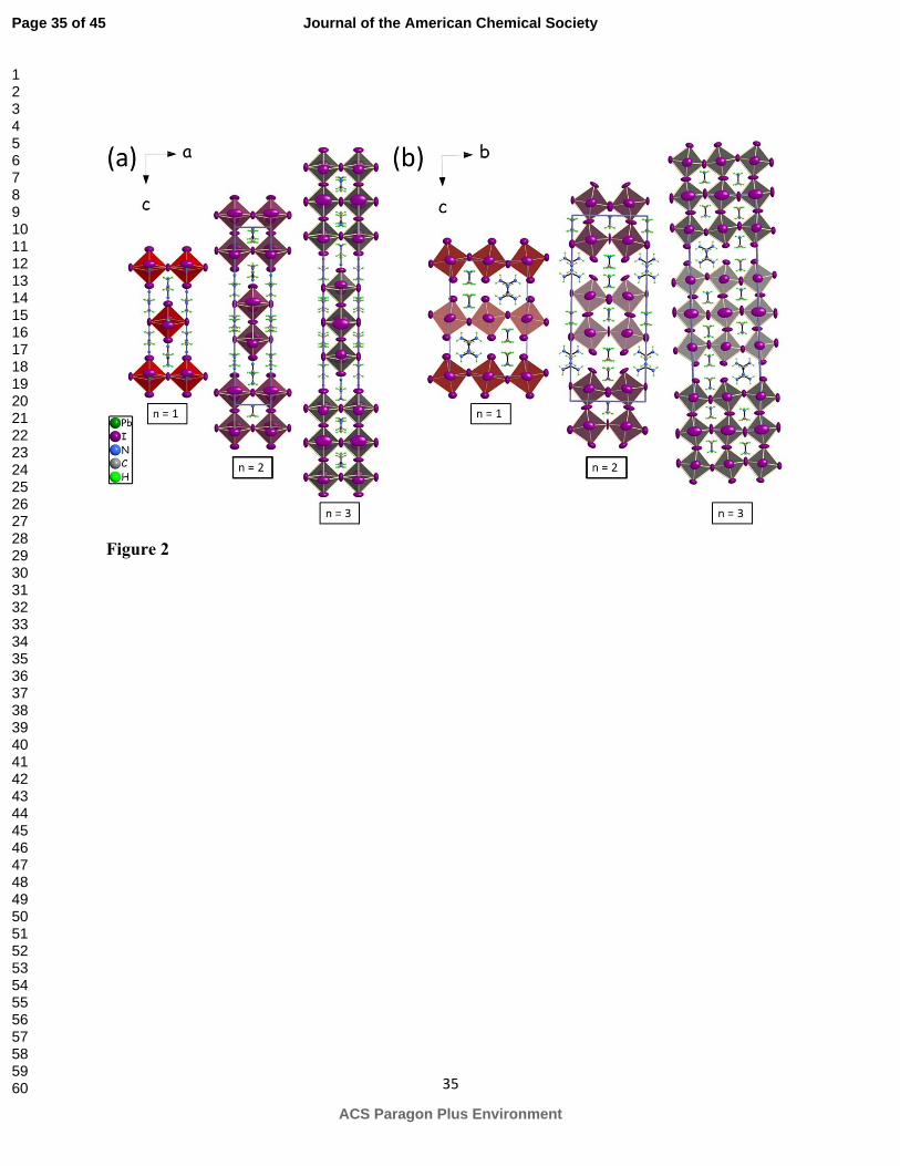
35
Figure 2
Page 35 of 45
ACS Paragon Plus Environment
Journal of the American Chemical Society
123456789101112131415161718192021222324252627282930313233343536373839404142434445464748495051525354555657585960

36
Figure 3
Page 36 of 45
ACS Paragon Plus Environment
Journal of the American Chemical Society
123456789101112131415161718192021222324252627282930313233343536373839404142434445464748495051525354555657585960

37
Figure 4
Page 37 of 45
ACS Paragon Plus Environment
Journal of the American Chemical Society
123456789101112131415161718192021222324252627282930313233343536373839404142434445464748495051525354555657585960

38
Figure 5
1.0 0.8 0.6 0.4 0.2 0.0500
550
600
650
700
750
800
PL emission /nm
1/n2
BA2MA
n-1Pb
nI3n+1
GAMAnPb
nI3n+1
2.4
2.2
2
1.8
1.6
PL emission /eV
500 600 7000.0
0.2
0.4
0.6
0.8
1.0
GAMAPbI4
BA2PbI
4
Wavelength /nm
PL Intensity
500 600 7000.0
0.2
0.4
0.6
0.8
1.0
Wavelength /nmWavelength /nm
GAMA2Pb
2I7
BA2MAPb
2I7
PL Intensity
500 600 7000.0
0.2
0.4
0.6
0.8
1.0
Wavelength /nm
GAMA3Pb
3I10
BA2MA
2Pb
3I10
PL Intensity
(a)
(c)
(b)
(d)
Page 38 of 45
ACS Paragon Plus Environment
Journal of the American Chemical Society
123456789101112131415161718192021222324252627282930313233343536373839404142434445464748495051525354555657585960

39
Figure 6
Page 39 of 45
ACS Paragon Plus Environment
Journal of the American Chemical Society
123456789101112131415161718192021222324252627282930313233343536373839404142434445464748495051525354555657585960
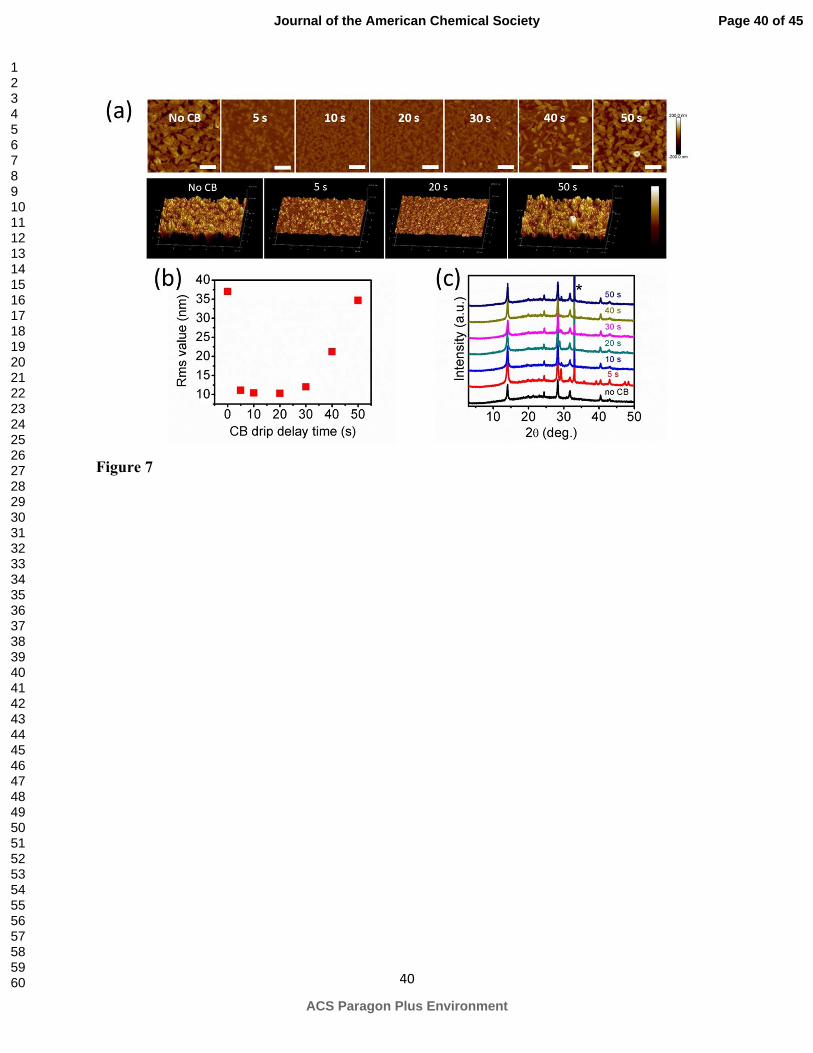
40
Figure 7
Page 40 of 45
ACS Paragon Plus Environment
Journal of the American Chemical Society
123456789101112131415161718192021222324252627282930313233343536373839404142434445464748495051525354555657585960

41
Figure 8
Page 41 of 45
ACS Paragon Plus Environment
Journal of the American Chemical Society
123456789101112131415161718192021222324252627282930313233343536373839404142434445464748495051525354555657585960

42
Table 1. Structural configurations of the three types of <100> 2D perovskites. RP DJ AV ACI
Formula (A′A)n+1BnX3n+1 A′ An–1BnX3n+1 (Bi2O2)A n-1BnX3n+1 (A′A)n+1BnX3n+1
Stacking sequence [(A′X)(ABX)n] [(A′)(An–1BX)n] [(Bi2O2)(A n-1BX)n] [(A′X)(ABX)n] Centering of perovskite slabsa I (½, ½, ½) P (0,0,0) I (½, ½, ½) A/B/C (½, 0, ½)
n = 3 exemplar Sr4Ti3O10 KCa2Nb3O10 (Bi2O2)SrTa2O9b,c (GA)(MA)3Pb3I10
a in the aristotype, ie. ignoring octahedral tilts
b The n = 2 is chosen for clarity; for the n = 3 member see reference
27
c Reference
74
Page 42 of 45
ACS Paragon Plus Environment
Journal of the American Chemical Society
123456789101112131415161718192021222324252627282930313233343536373839404142434445464748495051525354555657585960

43
Table 2. Crystal data and structure refinement for GAMAnPbnI3n+1 (n = 1-3) at 293 K. Formula GAMAPbI4 GAMA2Pb2I7 GAMA3Pb3I10
FW 807.0 1426.9 2046.9
Temperature (K) 293
Wavelength 0.71073 Å Refinement
method Full-matrix least-squares on F2
Crystal system orthorhombic
Space group Imma Bmm2 Imma
Unit cell dimensions (Å)
a = 6.4286(6) b = 12.4577(9) c = 18.8258(13)
a = 6.3729(4) b = 12.5435(8) c = 31.376(2)
a = 6.3520(7) b = 12.4378(9) c = 43.970(3)
Volume (Å3) 1507.7(2) 2508.2(3) 3473.8(5)
Z 4 4 4
ρcalc (g/cm3) 3.5551 3.7788 3.9138
µ (mm-1) 19.349 22.017 23.395
F(000) 1392 2424 3464 Crystal
size (mm3) 0.1111 x 0.0225 x 0.0167 0.0511 x 0.179 x 0.0100 0.0733 x 0.0372 x 0.0193
θ range (°) 3.27 to 29.23 2.6 to 29.27 2.78 to 29.29
Index ranges -8<=h<=8
-17<=k<=16 -25<=l<=25
-8<=h<=8 -17<=k<=17 -42<=l<=42
-8<=h<=8 -17<=k<=16 -57<=l<=60
Reflections collected
7172 11855 12119
Independent reflections
784 [Rint = 0.1277] 2595 [Rint = 0.0563] 1810 [Rint = 0.1261]
Completeness to θ 99% 99% 99% Data / restraints /
parameters 784 / 3 / 28 2595 / 9 / 82 1810 / 5 / 59
GOF 3.18 2.19 2.80
R indices [I>2σ(I)] Robs = 0.0575
wRobs = 0.1356 Robs = 0.0555
wRobs = 0.1099 Robs = 0.0597
wRobs = 0.1254
R indices [all data] Rall = 0.0677
wRall = 0.1361 Rall = 0.0898
wRall = 0.1126 Rall = 0.0863
wRall = 0.1270 Largest diff. peak and hole (e·Å-3)
1.84 and -2.31 5.69 and -1.65 3.32 and -3.20
R = Σ||Fo|-|Fc|| / Σ|Fo|, wR = {Σ[w(|Fo|2 - |Fc|
2)2] / Σ[w(|Fo|4)]}1/2 and w=1/(σ2(I)+0.0004I2)
Page 43 of 45
ACS Paragon Plus Environment
Journal of the American Chemical Society
123456789101112131415161718192021222324252627282930313233343536373839404142434445464748495051525354555657585960

44
Table 3. Bond lengths [Å] and angles (degrees) for GAMAPbI4, GAMA2Pb2I7, and GAMA3Pb3I10 at 293 K with estimated standard deviations in parentheses.
GAMAPbI4
Label Distances Label Angles
Pb(1)-I(1) 3.181(2) Pb(1)-I(2)-Pb(1)’ 180.0(5)
Pb(1)-I(2) 3.2143(6) Pb(1) -I(3)-Pb(1)’ 159.04(13)
Pb(1)-I(3) 3.1673(8)
GAMA2Pb2I7
Label Distances Label Angles
Pb(1)-I(1) 3.168(3) Pb(1)-I(1)-Pb(1)’ 159.8(4)
Pb(1)-I(4) 3.271(9) Pb(2)-I(2)-Pb(2)’ 159.4(5)
Pb(1)-I(5) 3.121(7) Pb(1)-I(4)-Pb(2) 166.13(14)
Pb(1)-I(6) 3.1910(6) Pb(1)-I(6)-Pb(1)’ 173.9(3)
Pb(1)-I(8) 3.181(3) Pb(1)-I(8)-Pb(1)’ 164.9(5)
Pb(2)-I(2) 3.205(4) Pb(2)-I(9)-Pb(2)’ 165.1(4)
Pb(2)-I(3) 3.097(7)
Pb(2)-I(4) 3.206(9)
Pb(2)-I(7) 3.1865(4)
Pb(2)-I(9) 3.145(3)
GAMA3Pb3I10
Label Distances Label Angles
Pb(1)-I(5) 3.154(3) Pb(2)-I(4)-Pb(2)’ 162.70(14)
Pb(1)-I(6) 3.1760(7) Pb(1)-I(5)-Pb(2) 167.66(11)
Pb(1)-I(7) 3.1280(7) Pb(1)-I(6)-Pb(1)’ 180.0(5)
Pb(2)-I(1) 3.092(2) Pb(1) -I(7)-Pb(1)’ 167.50(19)
Pb(2)-I(2) 3.1663(13)
Pb(2)-I(3) 3.1779(7)
Pb(2)-I(4) 3.1294(13)
Pb(2)-I(5) 3.264(3)
Page 44 of 45
ACS Paragon Plus Environment
Journal of the American Chemical Society
123456789101112131415161718192021222324252627282930313233343536373839404142434445464748495051525354555657585960

45
Table 4. Solar cell device parameters for GAMA3Pb
3I10
as a function of the delay in the anti-
solvent dripping. The average PCE is obtained from at least ten devices at each condition.
Delay time (s) Jsc [mA/cm2] Voc [V] FF [%] η[%]
3 s 6.781 0.863 69.07 4.04 (3.90 ± 0.18)
5 s 7.446 0.925 71.86 4.95 (4.33 ± 0.40)
10 s 8.668 1.033 76.08 6.81 (6.14 ± 0.36)
20 s 9.357 0.974 79.68 7.26 (6.69 ± 0.47)
30 s 8.833 0.970 78.01 6.68 (6.30 ± 0.59)
40 s 8.821 0.695 65.44 4.01 (3.84 ± 0.19)
50 s 8.989 0.554 60.83 3.03 (2.72 ± 0.28)
TOC Image
Page 45 of 45
ACS Paragon Plus Environment
Journal of the American Chemical Society
123456789101112131415161718192021222324252627282930313233343536373839404142434445464748495051525354555657585960

S1
Supporting Information
New Type of 2D Perovskites with Alternating Cations in the
Interlayer Space, (C(NH2)3)(CH3NH3)nPbnI3n+1: Structure,
Properties and Photovoltaic Performance
Chan Myae Myae Soe,1# Constantinos C. Stoumpos,1# Mika�̈�𝑒l Kepenekian,2 Boubacar Traoré,2
Hsinhan Tsai,3 Wanyi Nie,3 Binghao Wang,1 Claudine Katan,2 Ram Seshadri,4,5,6 Aditya D.
Mohite,3 Jacky Even,7 Tobin J. Marks,1 Mercouri G. Kanatzidis*1
1Department of Chemistry and Argonne-Northwestern Solar Energy Research Center, Northwestern
University, Evanston, Illinois 60208, USA 2 Institut des Sciences Chimiques de Rennes (ISCR), UMR 6226, CNRS - Université de Rennes 1 - Ecole
Nationale Supérieure de Chimie de Rennes - INSA Rennes, France 3Los Alamos National Laboratory, Los Alamos, NM 87545, USA 4Materials Research Laboratory, University of California, Santa Barbara, California 93106, USA 5Materials Department, University of California, Santa Barbara, California 93106, USA 6Department of Chemistry and Biochemistry, University of California, Santa Barbara, California 93106,
USA 7Fonctions Optiques pour les Technologies de l’Information (FOTON), UMR 6082, CNRS - INSA
Rennes - Université de Rennes 1, France
*Corresponding authors. E-mail: [email protected]

S2
Figure S1. Closeup view of the electronic band structure of the n = 2 member of the (GA)(MA)nPbnI3n+1 ACI perovskites, highlighting the Rashba splitting of the valence and conduction band extrema around the S point of the Brillouin zone.

S3
Figure S2. Dielectric profiles for (a) (GA)(MA)nPbnI3n+1, (b) (BA)2(MA)n-1PbnI3n+1 for n = 1 and n = 3. (c) Dielectric profile for bulk 3D MAPbI3. (d) Comparison between the dielectric profiles of RP and ACI layered perovskites with the same n-member, illustrating the net contribution of the spacer cations to the dielectric profile (green trace).
(a) (b) (c)
RP

S4
Figure S3. (a) PXRD patterns of thin films of (GA)(MA)2Pb2I7 and (GA)(MA)3Pb3I10 obtained from the chlorobenzene (CB) anti-solvent method. (b) Optical absorption spectra of thin films of (GA)(MA)2Pb2I7 and (GA)(MA)3Pb3I10 obtained from the anti-solvent method. (c) Efficiency vs. precursor solution concentration for devices made of (GA)(MA)3Pb3I10 using the anti-solvent method. (d) GIWAXS patterns of thin films of (GA)(MA)3Pb3I10 as a function of the delay in dripping time of the anti-solvent.

S5
Figure S4. Close up view of the PXRD pattern of a thin film of (GA)(MA)3Pb3I10 obtained from the anti-solvent method, referenced against the calculated patterns of (GA)(MA)3Pb3I10 and MAPbI3, highlighting the formation of the 2D ACI perovskite on the substrate.

S6
Table S1. Atomic coordinates (x104) and equivalent isotropic displacement parameters (Å2x10³) for GAMAPbI4 at 293 K with estimated standard deviations in parentheses. Label x y z Occupancy Ueq* Pb(1) 0 0 0 1 32(1) I(1) 0 418(2) 1667(2) 1 66(1) I(2) 5000 0 0 1 69(2) I(3) 0 7500 306(2) 1 78(2) N(1) 5000 2500 1110(50) 1 220(30) N(2) 0 7500 2231(15) 1 54(5) N(3) 0 8461(14) 3279(13) 1 54(5) C(1) 5000 2500 1910(50) 1 220(30) C(2) 0 7500 2948(15) 1 54(5) H(1n3) 0 8490.85 3740.93 1 64.8 H(2n3) 0 9050.08 3031.18 1 64.8 H(1n2) 0 6895.2 1999.53 1 64.8 H(2n2) 0 8104.8 1999.53 1 64.8 H(1n1) 5930.53 2950.49 956.76 0.25 265.7 H(2n1) 5290.76 1858.9 956.76 0.25 265.7 H(3n1) 3778.71 2690.61 956.76 0.25 265.7 H(1c1) 6221.29 2309.39 2061.62 0.25 265.7 H(2c1) 4709.24 3141.1 2061.62 0.25 265.7 H(3c1) 4069.47 2049.51 2061.62 0.25 265.7
*Ueq is defined as one third of the trace of the orthogonalized Uij tensor.

S7
Table S2. Atomic coordinates (x104) and equivalent isotropic displacement parameters (Å2x10³) for GAMA2Pb2I7 at 293 K with estimated standard deviations in parentheses. Label x y z Occupancy Ueq* Pb(1) 5000 2486(2) 3875(1) 1 32(2) Pb(2) 5000 2486(2) 1826(1) 1 33(2) I(1) 5000 0 4052(3) 1 83(5) I(2) 5000 5000 2009(4) 1 82(4) I(3) 5000 2889(7) 852(2) 1 69(3) I(4) 5000 2175(3) 2840(3) 1 84(2) I(5) 5000 2900(6) 4856(2) 1 67(3) I(6) 0 2516(10) 3822(3) 1 72(3) I(7) 0 2473(10) 1825(3) 1 75(3) I(8) 5000 5000 3742(4) 1 119(7) I(9) 5000 0 1696(3) 1 109(7) N(1) 0 0 2786(17) 1 103(19) N(2) 0 5000 2587(1) 1 500(100) N(3) 0 5000 1276(13) 1 65(14) N(4) 5000 5000 -260(30) 1 190(40) N(5) 5000 932(1) -180(20) 1 140(30) N(6) 5000 0 460(20) 1 140(30) N(7) 5000 986(12) 5810(11) 1 33(7) N(8) 5000 0 5208(10) 1 33(7) C(1) 0 0 3264(17) 1 103(19) C(2) 0 5000 3065(1) 1 500(100) C(3) 0 5000 798(13) 1 65(14) C(4) 5000 5000 220(30) 1 190(40) C(5) 5000 0 30(20) 1 140(30) C(6) 5000 0 5638(10) 1 33(7) H(1n1) 873.54 480.25 2693.79 0.25 123.3 H(2n1) 381.84 -624.48 2693.79 0.25 123.3 H(3n1) -1255.38 144.23 2693.79 0.25 123.3 H(1n2) 1277.74 4921.35 2494.7 0.25 596.4 H(2n2) -772.93 4477.13 2494.7 0.25 596.4 H(3n2) -504.8 5601.52 2494.7 0.25 596.4 H(1n3) -1011.97 4595.94 1368.49 0.25 78.5 H(2n3) 1194.73 4756.77 1368.49 0.25 78.5

S8
H(3n3) -182.76 5647.29 1368.49 0.25 78.5 H(1n4) 3758.24 4828 -351.94 0.25 229.2 H(2n4) 5327.7 5632.37 -351.94 0.25 229.2 H(3n4) 5914.06 4539.63 -351.94 0.25 229.2 H(1n5) 5000 932.01 -461.06 1 167.6 H(2n5) 5000 1532.67 -45.14 1 167.6 H(1n6) 5000 -600.66 600.24 0.5 167.6 H(2n6) 5000 600.66 600.24 0.5 167.6 H(1n7) 5000 1064.18 6085.52 1 39.8 H(2n7) 5000 1544.4 5645.3 1 39.8 H(1n8) 5000 -600.66 5069.11 0.5 39.8 H(2n8) 5000 600.66 5069.11 0.5 39.8 H(1c1) 966.4 -528.76 3366.27 0.25 123.3 H(2c1) 418.1 689.59 3366.27 0.25 123.3 H(3c1) -1384.5 -160.83 3366.27 0.25 123.3 H(1c2) 1416.32 4946.5 3167.17 0.25 596.4 H(2c2) -616.97 5649.92 3167.17 0.25 596.4 H(3c2) -799.35 4403.58 3167.17 0.25 596.4 H(1c3) 846.04 5579.56 696.02 0.25 78.5 H(2c3) 564.88 4337.96 696.02 0.25 78.5 H(3c3) -1410.92 5082.47 696.02 0.25 78.5 H(1c4) 4707.54 4293.9 320.55 0.25 229.2 H(2c4) 6349.82 5224.37 320.55 0.25 229.2 H(3c4) 3942.64 5481.73 320.55 0.25 229.2
*Ueq is defined as one third of the trace of the orthogonalized Uij tensor.
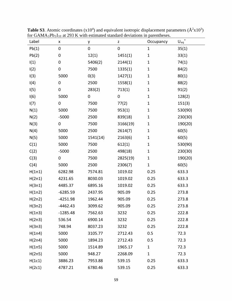
S9
Table S3. Atomic coordinates (x104) and equivalent isotropic displacement parameters (Å2x10³) for GAMA3Pb3I10 at 293 K with estimated standard deviations in parentheses. Label x y z Occupancy Ueq* Pb(1) 0 0 0 1 35(1) Pb(2) 0 12(1) 1451(1) 1 33(1) I(1) 0 5406(2) 2144(1) 1 74(1) I(2) 0 7500 1335(1) 1 84(2) I(3) 5000 0(3) 1427(1) 1 80(1) I(4) 0 2500 1558(1) 1 88(2) I(5) 0 283(2) 713(1) 1 91(2) I(6) 5000 0 0 1 128(2) I(7) 0 7500 77(2) 1 151(3) N(1) 5000 7500 953(1) 1 530(90) N(2) -5000 2500 839(18) 1 230(30) N(3) 0 7500 3166(19) 1 190(20) N(4) 5000 2500 2614(7) 1 60(5) N(5) 5000 1541(14) 2163(6) 1 60(5) C(1) 5000 7500 612(1) 1 530(90) C(2) -5000 2500 498(18) 1 230(30) C(3) 0 7500 2825(19) 1 190(20) C(4) 5000 2500 2306(7) 1 60(5) H(1n1) 6282.98 7574.81 1019.02 0.25 633.3 H(2n1) 4231.65 8030.03 1019.02 0.25 633.3 H(3n1) 4485.37 6895.16 1019.02 0.25 633.3 H(1n2) -6285.59 2437.95 905.09 0.25 273.8 H(2n2) -4251.98 1962.44 905.09 0.25 273.8 H(3n2) -4462.43 3099.62 905.09 0.25 273.8 H(1n3) -1285.48 7562.63 3232 0.25 222.8 H(2n3) 536.54 6900.14 3232 0.25 222.8 H(3n3) 748.94 8037.23 3232 0.25 222.8 H(1n4) 5000 3105.77 2712.43 0.5 72.3 H(2n4) 5000 1894.23 2712.43 0.5 72.3 H(1n5) 5000 1514.89 1965.17 1 72.3 H(2n5) 5000 948.27 2268.09 1 72.3 H(1c1) 3886.23 7953.88 539.15 0.25 633.3 H(2c1) 4787.21 6780.46 539.15 0.25 633.3

S10
H(3c1) 6326.56 7765.66 539.15 0.25 633.3 H(1c2) -6200.48 2107.99 425.22 0.25 273.8 H(2c2) -3735.01 2165.06 425.22 0.25 273.8 H(3c2) -5064.51 3226.95 425.22 0.25 273.8 H(1c3) 98.44 6774.04 2752.13 0.25 222.8 H(2c3) 1181.83 7906.52 2752.13 0.25 222.8 H(3c3) -1280.27 7819.44 2752.13 0.25 222.8
*Ueq is defined as one third of the trace of the orthogonalized Uij tensor.

S11
Table S4. Anisotropic displacement parameters (Å2x10³) for GAMAPbI4 at 293 K with estimated standard deviations in parentheses. Label U11 U22 U33 U12 U13 U23 Pb(1) 25(1) 28(1) 42(1) 0 0 3(1) I(1) 90(2) 63(2) 44(2) 0 0 -2(2) I(2) 21(2) 111(3) 74(2) 0 0 21(2) I(3) 155(4) 22(2) 57(2) 0 0 0
The anisotropic displacement factor exponent takes the form: -2π2[h2a*2U11 + ... + 2hka*b*U12]. Table S5. Anisotropic displacement parameters (Å2x10³) for GAMA2Pb2I7 at 293 K with estimated standard deviations in parentheses. Label U11 U22 U33 U12 U13 U23 Pb(1) 24(2) 26(3) 47(2) 0 0 1(2) Pb(2) 37(2) 28(3) 34(2) 0 0 0(2) I(1) 139(12) 35(5) 74(6) 0 0 0 I(2) 102(9) 40(6) 103(7) 0 0 0 I(3) 97(7) 75(5) 36(3) 0 0 34(2) I(4) 107(3) 119(3) 26(2) 0 0 -20(4) I(5) 91(7) 67(4) 43(3) 0 0 20(2) I(6) 18(3) 128(8) 72(4) 0 0 12(4) I(7) 26(3) 125(8) 72(3) 0 0 -25(4) I(8) 233(17) 6(4) 119(8) 0 0 0 I(9) 248(19) 13(5) 65(5) 0 0 0
The anisotropic displacement factor exponent takes the form: -2π2[h2a*2U11 + ... + 2hka*b*U12]. Table S6. Anisotropic displacement parameters (Å2x10³) for GAMA3Pb3I10 at 293 K with estimated standard deviations in parentheses. Label U11 U22 U33 U12 U13 U23 Pb(1) 37(1) 34(1) 35(1) 0 0 2(1) Pb(2) 31(1) 29(1) 38(1) 0 0 0(1) I(1) 116(2) 72(2) 35(2) 0 0 -10(1) I(2) 130(4) 25(2) 99(3) 0 0 0 I(3) 26(1) 123(2) 90(2) 0 0 -15(2) I(4) 172(4) 25(2) 68(3) 0 0 0 I(5) 120(2) 128(2) 26(2) 0 0 -2(2) I(6) 25(2) 250(5) 108(4) 0 0 -1(5) I(7) 304(8) 21(2) 128(5) 0 0 0
The anisotropic displacement factor exponent takes the form: -2π2[h2a*2U11 + ... + 2hka*b*U12].

S12
Table S7. Calculated band dispersion (meV) along the perovskite layer stacking direction in reciprocal space for ACI (GA)(MA)nPbnI3n+1 perovskites with n = 1-3.
n-member 1 2 3 k-direction W-T Γ-Y W-T
VBM (meV) 48 63 < 1 CBM (meV) 11 26 4


![Bandgap‐Tunable Cesium Lead Halide Perovskites with High … · and inorganic cesium (Cs) cations can be both structurally and thermally stable above 100 °C. [ 11,12 ] However,](https://img.dokumen.tips/doc/110x75/5e71ddd9b65e476b1d428c49/bandgapatunable-cesium-lead-halide-perovskites-with-high-and-inorganic-cesium.jpg)