Embed Size (px)
Citation preview

New Process Approaches to Metalorganic Vapor
Phase Epitaxy of III-nitrides for High Power HEMTs
Von der Fakultat fur Elektrotechnik und Informationstechnikder Rheinisch–Westfalischen Technischen Hochschule Aachen
zur Erlangung des akademischen Grades eines Doktors der Ingenieurwissenschaften,genehmigte Dissertation.
vorgelegt von
Diplom-Ingenieur
Roger Steinsaus Johannesburg, Sudafrika
Berichter: Universitatsprofessor Hans LuthUniversitatsprofessor Wilfried Mokwa
Tag der mundlichen Prufung: 10. August 2006
Diese Dissertation ist auf den Internetseiten der Hochschulbibliothek onlineverfugbar.

2


Contents
1 Introduction 1
1.1 Motivation . . . . . . . . . . . . . . . . . . . . . . . . . . . . . . . . . . . . 1
1.2 Scope of this Thesis . . . . . . . . . . . . . . . . . . . . . . . . . . . . . . . 4
2 Properties of III-Nitrides and their Application in HEMTs 7
2.1 Physical Properties . . . . . . . . . . . . . . . . . . . . . . . . . . . . . . . 7
2.2 Electrical Properties of Nitrides . . . . . . . . . . . . . . . . . . . . . . . . 8
2.2.1 Spontaneous and Piezoelectric Polarization . . . . . . . . . . . . . . 10
2.2.2 HEMT-Structures Based on AlGaN/GaN Heterojunctions . . . . . 13
3 Principles of MOVPE GaN Growth 19
3.1 MOVPE Process . . . . . . . . . . . . . . . . . . . . . . . . . . . . . . . . 19
3.1.1 General Considerations . . . . . . . . . . . . . . . . . . . . . . . . . 20
3.1.2 Thermodynamics . . . . . . . . . . . . . . . . . . . . . . . . . . . . 23
3.1.3 Kinetics . . . . . . . . . . . . . . . . . . . . . . . . . . . . . . . . . 25
3.1.4 Hydrodynamics and Mass Transport . . . . . . . . . . . . . . . . . 27
3.1.5 Influence of Carrier Gases . . . . . . . . . . . . . . . . . . . . . . . 32
3.2 Sapphire as Substrate for (Al)GaN growth . . . . . . . . . . . . . . . . . . 33
3.3 MOVPE III-nitride Growth . . . . . . . . . . . . . . . . . . . . . . . . . . 36
3.3.1 Modelling of GaN Growth . . . . . . . . . . . . . . . . . . . . . . . 38
i

ii CONTENTS
4 Experimental Setup and Characterization Methods 41
4.1 The Horizontal MOVPE Reactor (Aix 200 RF-S) . . . . . . . . . . . . . . 41
4.2 In-situ Monitoring . . . . . . . . . . . . . . . . . . . . . . . . . . . . . . . 44
4.2.1 In-situ Normalized Reflectometry . . . . . . . . . . . . . . . . . . . 45
4.2.2 Pyrometry . . . . . . . . . . . . . . . . . . . . . . . . . . . . . . . . 48
4.3 Ex-situ Characterization Methods . . . . . . . . . . . . . . . . . . . . . . . 52
4.3.1 Film Thickness and Homogeneity . . . . . . . . . . . . . . . . . . . 52
4.3.2 Differential Interference Contrast Microscopy . . . . . . . . . . . . . 53
4.3.3 Atomic Force Microscopy . . . . . . . . . . . . . . . . . . . . . . . . 54
4.3.4 Photoluminescence Spectroscopy . . . . . . . . . . . . . . . . . . . 55
4.3.5 X-ray diffraction . . . . . . . . . . . . . . . . . . . . . . . . . . . . 56
4.3.6 Rutherford Backscattering Spectroscopy . . . . . . . . . . . . . . . 57
4.3.7 Contactless Sheet Resistance Measurement . . . . . . . . . . . . . . 58
4.3.8 Hall Effect Measurement . . . . . . . . . . . . . . . . . . . . . . . . 59
5 Determination of Surface Temperature on Transparent Substrates 61
5.1 Standard Measurement Techniques vs. Emissivity Corrected Pyrometry . . 61
5.2 Conventional Calibration Methods . . . . . . . . . . . . . . . . . . . . . . . 62
5.3 New Calibration Approach with SiC Band Temperature Dependence . . . . 64
5.4 Limitations . . . . . . . . . . . . . . . . . . . . . . . . . . . . . . . . . . . 67
5.5 Conclusion . . . . . . . . . . . . . . . . . . . . . . . . . . . . . . . . . . . . 69
6 New Growth Approach for GaN 71
6.1 Morphological Development of MOVPE GaN . . . . . . . . . . . . . . . . . 71
6.2 Growth Reproducibility Issues . . . . . . . . . . . . . . . . . . . . . . . . . 75
6.3 New Process Approach: The Inverted Inlet Configuration . . . . . . . . . . 78
6.3.1 Growth Modelling . . . . . . . . . . . . . . . . . . . . . . . . . . . . 79

CONTENTS iii
6.3.2 Experimental Verification: Inverted to Conventional Inlet . . . . . . 83
6.3.3 Conclusion . . . . . . . . . . . . . . . . . . . . . . . . . . . . . . . . 87
7 Optimizing GaN Growth 89
7.1 Homogeneity Optimization . . . . . . . . . . . . . . . . . . . . . . . . . . . 89
7.1.1 Optimization Strategy . . . . . . . . . . . . . . . . . . . . . . . . . 90
7.1.2 Experimental Results . . . . . . . . . . . . . . . . . . . . . . . . . . 92
7.1.3 Modelling Verification . . . . . . . . . . . . . . . . . . . . . . . . . 94
7.1.4 Conclusion . . . . . . . . . . . . . . . . . . . . . . . . . . . . . . . . 96
7.2 On the Effect of N2 on GaN Growth . . . . . . . . . . . . . . . . . . . . . 97
7.2.1 Experimental Results . . . . . . . . . . . . . . . . . . . . . . . . . . 97
7.2.2 Conclusion . . . . . . . . . . . . . . . . . . . . . . . . . . . . . . . . 103
7.3 Electrical and Structural Optimization with Nitrogen . . . . . . . . . . . . 103
7.3.1 Aim to Prolong Coalescence in N2 . . . . . . . . . . . . . . . . . . . 103
7.3.2 Role of Nitrogen in 2D Growth . . . . . . . . . . . . . . . . . . . . 105
7.3.3 Optimizing GaN . . . . . . . . . . . . . . . . . . . . . . . . . . . . 106
7.3.4 Conclusion . . . . . . . . . . . . . . . . . . . . . . . . . . . . . . . . 111
8 HEMT growth 113
8.1 AlGaN Growth in the inverted inlet . . . . . . . . . . . . . . . . . . . . . . 114
8.1.1 Thickness and Alloy Composition control . . . . . . . . . . . . . . . 114
8.1.2 Thin AlGaN/GaN layers . . . . . . . . . . . . . . . . . . . . . . . . 117
8.1.3 Conclusion . . . . . . . . . . . . . . . . . . . . . . . . . . . . . . . . 119
8.2 Highly resistive GaN buffer . . . . . . . . . . . . . . . . . . . . . . . . . . . 121
8.2.1 Strategy for Semi-Insulating GaN . . . . . . . . . . . . . . . . . . . 121
8.2.2 Influence of Carrier Gas on Resistance . . . . . . . . . . . . . . . . 123
8.2.3 Conclusion . . . . . . . . . . . . . . . . . . . . . . . . . . . . . . . . 131

iv CONTENTS
8.3 HEMT results . . . . . . . . . . . . . . . . . . . . . . . . . . . . . . . . . . 132
9 Summary and Conclusions 137
References 141
Danksagung 149
List of Figures
2.1 Stick and ball diagram of wurtzitic GaN. According to the ionic radii thesmall spheres represent nitrogen while the big ones represent Gallium. . . . 8
2.2 Different polarities (Ga- and N faced) of wurtzite GaN [Amb98]. . . . . . . 10
2.3 Bandgaps of important binary semiconductors. . . . . . . . . . . . . . . . . 11
2.4 Sum of the microscopic dipoles, resulting in a spontaneous polarization 6= 0in the wurtzite structure (right) and = 0 in the zincblende (left). . . . . . . 12
2.5 Band diagram of the heterostructure formed by lightly n-doped narrow gapsemiconductor I and heavily n-doped wide gap semiconductor II dividedone from another (a) and together in thermodynamical equilibrium [Iba99]. 14
2.6 Polarisation induced charge in a Ga-faced (a) and N-faced (b) AlGaN/GaNheterostructure . . . . . . . . . . . . . . . . . . . . . . . . . . . . . . . . . 15
2.7 Dependence of the 2DEG mobility on the temperature and scattering mech-anisms for AlGaN/GaN heterostructures [Jen01]. . . . . . . . . . . . . . . 17
3.1 Process steps in CVD reactions . . . . . . . . . . . . . . . . . . . . . . . . 21
3.2 Typical Arrhenius plot of a CVD deposition process . . . . . . . . . . . . . 22
3.3 Schematic of the formation heat as a function of the distance along thereaction path. . . . . . . . . . . . . . . . . . . . . . . . . . . . . . . . . . . 26
3.4 Adatom motion and preferred adsorption at kinks and islands. . . . . . . . 27
3.5 Schematic diagram of the Rayleigh number versus the Reynolds number,classifying the different flow behavior expected in horizontal CVD reactors[Jen93]. . . . . . . . . . . . . . . . . . . . . . . . . . . . . . . . . . . . . . 31
3.6 Structure of an epilayer under biaxial compression. Pseudomorphic (left)and relaxed (right) with misfit dislocations. . . . . . . . . . . . . . . . . . . 34
v

vi LIST OF FIGURES
3.7 Rhombohedral structure and surface planes of the sapphire substrate. . . . 35
3.8 Growth model for GaN on sapphire substrates. . . . . . . . . . . . . . . . . 37
3.9 Schematic of the GaN decomposition and reaction pathways. Activationenergy (kcal/mol) is shown for each reaction pathway. Here, GaN* andGa* are adsorption species on the surface. Based on the work of Mihopoulos[Mih99] . . . . . . . . . . . . . . . . . . . . . . . . . . . . . . . . . . . . . 39
4.1 The AIX 200/4 horizontal reactor equipped with in-situ reflectometry andpyrometry (EpiR-TT) . . . . . . . . . . . . . . . . . . . . . . . . . . . . . 43
4.2 Schematic representation of the AIX 200/4 RF-S horizontal reactor em-ployed for the MOVPE growth of group III nitrides. Note, that the inletof group V and III is the conventional state on this sketch. . . . . . . . . . 44
4.3 Schematic of the in-situ reflectometer as used for measurements on rotatingsamples to detect the reflection [Hab02]. . . . . . . . . . . . . . . . . . . . 45
4.4 Schematic diagram illustrating the normalized reflectance. Layer B is nor-malized to the reflectance of layer A [Hab02]. . . . . . . . . . . . . . . . . . 46
4.5 Typical reflectance transient measured at a wavelength of 600 nm. . . . . . 47
4.6 Spectral radiance of a blackbody from Planck’s radiation law for severaltemperatures. . . . . . . . . . . . . . . . . . . . . . . . . . . . . . . . . . . 49
4.7 Spectral radiances for a blackbody and a graybody with emissivity of 0.5 atseveral temperatures, illustrating why accurate knowledge of the emissivityis essential. . . . . . . . . . . . . . . . . . . . . . . . . . . . . . . . . . . . 50
4.8 Pyrometry from opaque wafers such as Si or GaAs is a straightforward taskas seen on the left half. The emissivity (ε) of the substrate surface can becalculated from the measured reflectivity. On transparent substrates thepyrometer detects the emissivity of the underlying holder rather than thatof the transparent substrate. . . . . . . . . . . . . . . . . . . . . . . . . . . 51
4.9 Calibration run based on the Si-Al-eutectic formation at T = 577C wherea sudden roughening of the surface leads to a dramatic loss in reflectance.Experiment conducted at the Ferdinand Braun Institute Berlin in an AIX200/4 . . . . . . . . . . . . . . . . . . . . . . . . . . . . . . . . . . . . . . . 52
4.10 Schematic of Differential Interference Contrast. . . . . . . . . . . . . . . . 53
4.11 A smooth surface revealing terrace like steps of a GaN layer, as seen byAFM. . . . . . . . . . . . . . . . . . . . . . . . . . . . . . . . . . . . . . . 55

LIST OF FIGURES vii
4.12 Recombination processes for a direct band gap semiconductor. (A) BandBand Transition (e, h), (B) Band Acceptor Transition (e, A0), (C) DonorAcceptor Pair Transition (D0, A0), (D) Excitons. . . . . . . . . . . . . . . . 56
4.13 RBS spectrum of an AlxGa1−xN/GaN layer. The zigzag line is the RBSspectrum acquired in random geometry and the continuous line representsthe best fit from which the AlxGa1−xN layer composition (35 at% Al, 65at% Ga) and the thickness (27 nm) were determined. . . . . . . . . . . . . 58
5.1 Temperature offset between wafer surface and process control temperatureas determined by ECP and a light pipe pyrometer respectively for increas-ing rotation flows. . . . . . . . . . . . . . . . . . . . . . . . . . . . . . . . . 62
5.2 Reflectance and temperature transient of calibration run based on meltingpoint determination of a thin Ag layer on sapphire. The unexpected anduntimely slow degradation of the Ag-layer at a temperature of 570C ishighlighted. . . . . . . . . . . . . . . . . . . . . . . . . . . . . . . . . . . . 63
5.3 Reflection raw signal from SiC (double side polished, undoped) for twotemperatures. . . . . . . . . . . . . . . . . . . . . . . . . . . . . . . . . . . 65
5.4 Normalized reflectance spectra referenced to the room temperature spec-trum of an undoped double side polished SiC wafer for a range of absolutetemperatures. The straight lines represent the fit function used to deter-mine the onset of the absorption. . . . . . . . . . . . . . . . . . . . . . . . 66
5.5 The resulting correlation between absorption onset and absolute tempera-ture as found at the reference reactor (Ferdinand-Braun-Institut). . . . . . 67
5.6 Referencing our temperature, empty circles, to the absolute temperature,full circles. The true surface temperature of the SiC wafer at a processcontrol temperature T1=620 C is at 550 C and for T1=1050 C it is 950C. . . . . . . . . . . . . . . . . . . . . . . . . . . . . . . . . . . . . . . . . 68
5.7 Doping dependence of the energy bandgap of SiC . . . . . . . . . . . . . . 69
6.1 Typical reflectance transient (black line) and temperature (grey line) recordedduring a standard growth run of GaN on sapphire. AFM insets show themorphology at different stages of growth: Nucleation layer before (a) andafter recrystallization (b), during the evolution of island coalescence (c)and the final surface with atomic steps after coalescence (d). . . . . . . . . 73
6.2 Comparison of two nominally identical growth runs: The right transientdemonstrates a higher growth rate. The coalescence mode is also distinctlychanged. . . . . . . . . . . . . . . . . . . . . . . . . . . . . . . . . . . . . . 76

viii LIST OF FIGURES
6.3 Comparison of control temperature (light pipe) at 1180 C with surfacetemperature for a series of successive growth runs. The surface temperaturechanges here in the range of 14 K and the absolute temperature differenceis more than 50 K. . . . . . . . . . . . . . . . . . . . . . . . . . . . . . . . 77
6.4 Parasitic liner deposits at the liner ceiling . . . . . . . . . . . . . . . . . . 78
6.5 Sketch of inlet configuration and modelling of flow patterns: comparison forthe conventional (a) and the inverted inlet (b) geometry. The flow velocityis high on the ammonia channel side because of a high mass flow and acomparably small cross sectional area where the mass flow passes through.Thus, for the conventional inlet the flow is directed towards the ceiling bya vortex. The inverted case demonstrates no such effects. . . . . . . . . . . 79
6.6 Temperature distribution in a cross sectional view and on the liner ceiling. 80
6.7 Comparison of NH3 and TMGa distribution for the conventional (a) andthe inverted inlet (b) geometry. The concentrations are translated intocolors: blue for low and red for high concentrations. The ammonia andTMGa concentration close to the ceiling is higher for the conventional inletconfiguration. . . . . . . . . . . . . . . . . . . . . . . . . . . . . . . . . . . 81
6.8 Modeling: Comparison of MMGa distribution for the conventional (a) andthe inverted inlet (b) geometry. A transversal cross-section of the reactor ispresented. The concentrations are translated into colors: blue for low andred for high concentrations. The MMGa concentration is lower towards theceiling and higher towards the substrate in the inverted inlet configuration 82
6.9 Expected growth profiles according to modelling in flow direction over themiddle of the wafer. For the conventional inlet (lower line) a growth max-imum is expected in the middle of the wafer. The inverted inlet (upperline) geometry exhibits a maximum at the front of the wafer. . . . . . . . . 83
6.10 Comparison of growth rate distribution over the ceiling of the horizontalreactor above the substrate (marked with a circle) for the conventional(upper image) and the inverted inlet (lower image) geometry. The growthrates are translated into colors: blue for low and red for high rates. Thegrowth rate is more than three times as high for the conventional inletcompared to the inverted inlet. The deposition maximum is positionedupstream of the substrate for the conventional inlet. . . . . . . . . . . . . . 84
6.11 Comparison of transients (reflection measurement taken from the wafermiddle) for both growth processes. The coalescence time is significantlyshorter and the growth rate in the HT regime lower for the inverted inletgeometry. . . . . . . . . . . . . . . . . . . . . . . . . . . . . . . . . . . . . 85

LIST OF FIGURES ix
6.12 GaN growth profiles obtained using the conventional inlet (a) and the in-verted inlet (b) geometry. For the conventional inlet a convex growth profileis observed, for the inverted inlet a concave profile is found. . . . . . . . . . 85
6.13 Comparison of surface morphology at microscopic (upper image) and nanome-ter scale (lower image)for both processes. The AFM inset shows a slightlyrougher surface for the inverted inlet. . . . . . . . . . . . . . . . . . . . . . 86
7.1 Forced convection and Fickian diffusion dominate the distribution of growthlimiting species in the reactor and thus the homogeneity over the wafer.Forced convection moves the species in flow direction and parallel to thesubstrate surface, while diffusion moves the species perpendicular to theflow direction and to the substrate surface. . . . . . . . . . . . . . . . . . . 90
7.2 Inverted inlet geometry. The group III and group V sources are injectedthrough two separate channels. The upper channel contains the group Vsource (NH3) and the lower one the group III (TMGa) sources. For theuniformity investigation the total amount of hydrogen or nitrogen carriergas on the MO channel was increased stepwise . . . . . . . . . . . . . . . . 93
7.3 Standard deviation in thickness (left) and growth rate (right) in the in-verted inlet as a function of different amounts of hydrogen (boxes) andnitrogen (circles) in the carrier gas. . . . . . . . . . . . . . . . . . . . . . . 94
7.4 MMGa molar fraction distribution in a horizontal cross-section of the re-actor. Without nitrogen (upper image) and with nitrogen (lower image)supply through the lower inlet. Red shift means higher MMGa molar fraction. 95
7.5 Instant growth rate mappings for the regimes without nitrogen (left) andwith nitrogen (right) supply through the lower inlet. Less curved isolinesare achieved with nitrogen. . . . . . . . . . . . . . . . . . . . . . . . . . . . 96
7.6 Growth rate distribution for rotated wafers along the wafer centerline forthe regimes without nitrogen (upper line) and with nitrogen (lower line)supply through the lower inlet. Absolute growth rate values are over esti-mated by modelling. . . . . . . . . . . . . . . . . . . . . . . . . . . . . . . 96
7.7 Nomarski-microscopy of samples grown with increasing amount of nitrogenin the ambient. In case of pure nitrogen the surface drastically worsens.Hexagonal structures and even small ”turrets” can be observed. . . . . . . 98
7.8 AFM micrographs of GaN layers grown under pure H2 (left) or N2 (right). 98
7.9 The rocking curves of the (002) demonstrate similar FWHM values of about330arcsec, while the (102) peaks increases significantly. . . . . . . . . . . . 99
x LIST OF FIGURES
7.10 The donor bound exciton (DBX) peak is shifted towards lesser energiesfor an epitaxial growth run in pure nitrogen ambient in comparison to agrowth run in pure H2. . . . . . . . . . . . . . . . . . . . . . . . . . . . . . 100
7.11 Hall measurements at room temperature. . . . . . . . . . . . . . . . . . . . 101
7.12 Effect of nitrogen on the coalescence time and thickness. With increasingnitrogen content in the gas phase the coalescence time (and therefore the“coalescence thickness”) decreases drastically. . . . . . . . . . . . . . . . . 102
7.13 Reflectance transients of two growth runs in pure nitrogen ambient. Pro-longed coalescence in neither achieved by applying a lower coalescence tem-perature Tc nor lower V/III ratio. . . . . . . . . . . . . . . . . . . . . . . . 104
7.14 Growth transients: GaN is grown in different carrier gas mixtures on a”hydrogen template”. The carrier gas composition was changed stepwisetowards pure nitrogen, after the GaN film fully coalesced in H2 ambient . . 105
7.15 With increasing TMGa flow in the gasphase the coalescence time is almosthalved, while the coalescence thickness is constant (left). This affects alsothe electrical data (right): The shorter the coalescence time (with higherTMGa flow) the lower the mobility. . . . . . . . . . . . . . . . . . . . . . . 107
7.16 Applying a lower growth rate in combination with a reduced V/III ra-tio during the initial stages of growth results in an optimized coalescencegrowth rate and a thicker “coalescence layer” . . . . . . . . . . . . . . . . . 108
7.17 Symmetric (002) and asymmetric (102) reflections of GaN grown with de-creasing V/III ratio during coalescence reveal a significant structural im-provement. . . . . . . . . . . . . . . . . . . . . . . . . . . . . . . . . . . . . 109
7.18 Nomarski images: The longer the coalescence the more structured the sur-face gets. . . . . . . . . . . . . . . . . . . . . . . . . . . . . . . . . . . . . . 110
7.19 Comparison between the GaN grown in pure hydrogen to the finally fully”optimized GaN”. . . . . . . . . . . . . . . . . . . . . . . . . . . . . . . . . 111
8.1 Al solid-vapor relationship (left) and AlGaN growth rate for various Al gasphase concentrations (right). The dashed line in the left inset marks theideal vapor solid relationship, whereas boxes and dots represent measure-ment results from XRD and RBS respectively. The growth rate (right)decreases with increasing aluminum in the gas phase. . . . . . . . . . . . . 115
8.2 Alloy composition distribution for several runs at different positions overthe wafer in the inverted inlet configuration. . . . . . . . . . . . . . . . . . 116

LIST OF FIGURES xi
8.3 Heterostructure stacks grown on ”optimized GaN” in hydrogen (left) ornitrogen (right) ambient. Structure, thickness and composition are tem-perature independent, however, different for hydrogen and nitrogen. . . . . 118
8.4 AFM images of AlGaN layers grown in hydrogen (upper row) or nitrogenatmosphere (lower row). . . . . . . . . . . . . . . . . . . . . . . . . . . . . 119
8.5 Sheet carrier concentration for the AlGaN temperature series in hydrogen(left) and nitrogen (right) measured at room and liquid nitrogen temperature.120
8.6 Sheet conductivity (µ×ns) values for each series (hydrogen left and nitrogenright). . . . . . . . . . . . . . . . . . . . . . . . . . . . . . . . . . . . . . . 120
8.7 Comparison of two growth runs: The ”optimized GaN” with the two stepHT growth, consisting of the low growth rate and V/III ratio during co-alescence and the higher growth rate and V/III ratio during 2D growth(”2step”), in comparison with GaN grown in 75% nitrogen ambient (”1step”).124
8.8 Sheet resistance as a function of nitrogen percentage in the carrier gas. . . 125
8.9 AFM images of the AlGaN/GaN heterostructure on ”optimized GaN” (left)and ”N2 GaN” (right). . . . . . . . . . . . . . . . . . . . . . . . . . . . . . 126
8.10 With increasing HT-step growth temperature the formation of bigger de-fects such as turrets accelerates. Surface temperatures beyond 1130Cresult in hexagonal defects and pits on the surface. . . . . . . . . . . . . . 127
8.11 Resistance characterization procedure for the anneal time series. By locallyetching the AlGaN layer solely the GaN buffer is characterized. . . . . . . 127
8.12 Reflectance transients for several growth runs with different annealing times.Values are given for the reflectance differences between oscillation minimumand maximum. . . . . . . . . . . . . . . . . . . . . . . . . . . . . . . . . . 128
8.13 Broad increase in sheet resistance and resistivity over two orders of mag-nitude (left). Associated with the resistance is the rising FWHM value ofthe asymmetric (102) peak (right) . . . . . . . . . . . . . . . . . . . . . . . 129
8.14 Nomarski images of the annealing series. The morphology on the microm-eter scale smoothes with decreasing anneal time and also the density ofdefects clearly diminishes. . . . . . . . . . . . . . . . . . . . . . . . . . . . 130
8.15 AFM images of the anneal series. Anneal times decrease from left (2 min)to right (0 min). The surface morphology is quite similar to the earliergrown N2 samples (Figure 7.8). Round steps and pits are found. It seemsas if the surface becomes even more cauliflower like with decreasing annealtimes. . . . . . . . . . . . . . . . . . . . . . . . . . . . . . . . . . . . . . . 131

xii LIST OF FIGURES
8.16 Schematic drawing of a HEMT structure (left) and a real processed HEMT(right). . . . . . . . . . . . . . . . . . . . . . . . . . . . . . . . . . . . . . . 132
8.17 DC output characteristics for a gate bias from 1 to -7 V of two samplesgrown on different GaN buffers. Lg = 0.9 µm; Wg = 200 µm . . . . . . . . 133
8.18 Transfer characteristics of the HEMT structures. . . . . . . . . . . . . . . . 134

List of Tables
2.1 Crystal properties of GaN and AlN [Edg94] [Fou03]. . . . . . . . . . . . . . 9
3.1 Lattice constant and thermal expansion coefficient for heteroepitaxy ofGaN on different substrates [Gil98]. . . . . . . . . . . . . . . . . . . . . . . 34
6.1 Boundary conditions for a standard GaN growth process . . . . . . . . . . 80
6.2 Comparison of morphological, structural, electrical and uniformity data forthe conventional and inverted inlet geometries . . . . . . . . . . . . . . . . 86
7.1 Growth parameters for a standard GaN growth process in an AIX 200/4RF-S reactor (TMGa bubbler was used at a pressure of 1000 mbar and atemperature of 0C) . . . . . . . . . . . . . . . . . . . . . . . . . . . . . . 92
7.2 Growth parameters for the GaN growth process with increasing nitrogenamount in the gas phase . . . . . . . . . . . . . . . . . . . . . . . . . . . . 97
7.3 Growth parameters for the prolonged coalescence run in nitrogen ambient. 104
7.4 Properties of GaN layers with hydrogen coalescence and different amountof nitrogen during 2D growth. . . . . . . . . . . . . . . . . . . . . . . . . . 106
7.5 Growth parameters for prolonged coalescence in a 85% N2/ 15 % H2 carriergas mixture. . . . . . . . . . . . . . . . . . . . . . . . . . . . . . . . . . . . 107
7.6 Growth parameters for prolonged coalescence run in nitrogen ambient. . . 109
7.7 Improved electrical and structural data of the GaN film with lowering theV/III ratio, thus prolonging coalescence. . . . . . . . . . . . . . . . . . . . 110
8.1 Growth parameters for the AlGaN growth. . . . . . . . . . . . . . . . . . . 114
xiii

xiv LIST OF TABLES
8.2 Growth parameters for AlGaN growth at 9 slm in two commonly appliedcarrier gas mixtures . . . . . . . . . . . . . . . . . . . . . . . . . . . . . . . 116
8.3 Growth parameters for thin AlGaN growth at 9 slm in two commonlyapplied carrier gas mixtures . . . . . . . . . . . . . . . . . . . . . . . . . . 117
8.4 Growth parameters for the ”optimized GaN” template. . . . . . . . . . . . 123
8.5 Sheet resistance and structural quality of the ”optimized GaN” layer (2step)versus a non optimized growth run in 75% nitrogen (1step). . . . . . . . . 123
8.6 Parameters for undoped GaN growth with increasing nitrogen amount inthe gas phase . . . . . . . . . . . . . . . . . . . . . . . . . . . . . . . . . . 124
Chapter 1
Introduction
1.1 Motivation
In the last 60 years semiconductor technology developed from one germanium based,matchbox sized single transistor at Bell Labs to millions of silicon based transistors on anarea the size of a thumbnail in every day use. Thanks to Moore’s Law the cycle of increas-ing performance and shrinking size keeps going. The leading role in the semiconductorbusiness is still played by silicon, because it has many beneficial properties for deviceapplications. It is abundant in nature, non toxic, easy to process and is one of the bestcharacterized material systems. However, silicon also has significant weaknesses whenit comes to optoelectronics or high frequency applications. Silicon is an indirect semi-conductor, which greatly reduces its efficiency in light generation like in light emittingdiodes (LEDs). Also, many III-V compounds have far smaller effective electron massesthan the group IV materials like Si and Ge. Simplified, electronic transport depends onthe maximum obtainable charge carrier velocity, which is inversely proportional to theeffective mass. Thus, the ultimate speed of integrated circuits depends on the carriervelocity, so the low effective mass is one of the fundamental reasons that GaAs and otherIII-V compounds are used instead of Si in high-bandwidth and low noise applications likesatellite communication and radar. If additionally high power applications are envisaged,wide bandgap semiconductors are employed such as the III-nitrides.
Recent progress in epitaxial and bulk growth of GaN and related compounds make thesematerials viable contenders for a variety of different applications from light emitters inthe visible range (where III-nitride based technology is already commercialized) to highfrequency and high power devices. The properties of the group III nitrides have often beencited: They cover a wide bandgap range of 0.7eV (InN) to 6.2 eV (AlN). In comparison toother materials they have higher binding energies, making them mechanically very stable.The 3.4 eV bandgap of GaN predicts that it withstands 7.5 times the electric field that
1

2 CHAPTER 1. INTRODUCTION
GaAs can before avalanche breakdown occurs. The good electron transport properties ofGaN, with an electron mobility value possibly in excess of 2000cm2/V s and an averageelectron saturation velocity above 2 × 107cm/s make the material attractive for highfrequency application. All in all the nitrides are favorable when it comes to applicationsin hazardous environments, in high-temperature -frequency and -power regimes. Yet,GaN based RF components are not commercialized and will have to compete with theprevailing silicon based LDMOS devices or even SiGe, with less favorable properties inthis application field but low production costs.
Despite these prospects, single crystalline GaN films still need to be grown heteroepitax-ially on substrates like sapphire or SiC, which match more or less closely to its latticeconstants and thermal expansion coefficient, since -up to now- there is no commerciallyavailable substrate for homoepitaxy. In the beginning of GaN epitaxy the heteroepitaxysignificantly affected the quality of the material. High defect and dislocation densities(∼ 1010cm−2) resulted from the lattice mismatch. High impurity levels had the effect of avery high n-type background carrier concentration (∼ 1019− 1020 cm−3), which made theconductivity control, necessary for device applications, impossible. The problems relatedto the heteroepitaxial growth of GaN were first overcome by Amano and Akasaki in 1986[Ama86]. They introduced a thin AlN layer, grown on sapphire at lower temperature(LT) than the subsequent GaN layer, in a so-called two-step growth technique. Later,Nakamura used GaN as low temperature layer [Nak91]. In fact, this LT-layer, the socalled nucleation layer, acts like a template between the substrate and the epitaxial layer,resulting in a significant improvement of the material quality of the subsequent GaN lay-ers with dislocation densities ∼ 108cm−2 and a dramatic reduction of the backgrounddoping concentration (≤1017 cm−3). These developments also set the stage for the p-typeGaN doped with Mg in 1989, which was not possible until then. With these findings thefeasibility of the nitrides for device application came into focus and gave a great boost tonitride research.
Nowadays, the quality improvement of GaN-based materials is at a point where highperformance electronic devices can be produced. Of great technological interest for appli-cations such as sensors, radar, satellite, wireless base stations and power applications arehigh electron mobility transistors (HEMTs), which are by far the best investigated group-III nitrides electronic devices. The electron mobility is quite high in AlxGa1−xN/GaNheterostructures where two-dimensional electron gases (2DEG) form. The sheet con-ductivity in GaN based HEMTs, as the product of carrier concentration and mobilityis further enhanced by the strong piezoelectric and polarization effects present, whichaccount for the high carrier concentration in the 2DEG without doping. The nitridestherefore intrinsically fulfill another demand on HEMT structures: For high power andhigh speed performance it is of primal importance to maximize the channel sheet carrierconcentration without reducing electron mobility and saturation velocity. These facts incombination with the aforementioned material properties of the wide band gap nitridesallow a proportionately higher operating voltage and current for the same load impedance
1.1. MOTIVATION 3
in comparison to GaAs based heterostructures. When voltage and current are taken to-gether, a power delivery greater than 50 times that of GaAs devices is possible usingGaN-based HEMTs. It is this potential increase in power performance that acts as agreat motivator for pursuing GaN-based devices and circuits.
In order to achieve this goal, special care must be taken in the choice and preparationof a template. An ideal template for AlxGa1−xN/GaN heteroepitaxy with respect to theHEMT application must possess:
1. good structural quality with low dislocation densities for high amplification by highchannel conductivity at high frequencies;
2. a smooth surface with a low defect density, important for the growth of sharpinterfaces and flat surfaces as well as for device processing;
3. semi-insulating properties to avoid any parallel conductivity to the channel layerand to ensure high HEMT performance at high frequency;
4. high thermal conductivity to improve the dissipation of heat produced in the devicein high power applications;
5. ”manufacturing uniformity” in terms of homogenous layer characteristics and re-producible layer growth with a high yield, because high cost represent a significantroad block in the development of RF devices.
Moreover, the thickness and the composition of the subsequent AlxGa1−xN layer must befinely tuned in order to obtain a structural perfection at the AlxGa1−xN/GaN interface.The material grower must understand and solve all these growth issues related to group-IIInitrides in order to create a suitable nitride heterostructure for HEMT application.
Metal organic chemical vapor deposition (MOVPE) is the most successful and suitablegrowth method for obtaining high quality group III nitride based materials. Nevertheless,the number of process parameters to tune the growth is very large (e.g. temperatures,thicknesses, molar flow rates and ratios...) and due to the coupling between them, therole of each is not clearly understood. Although a tremendous amount of work has beendone these last years on optimizing the process parameters, a lot is still to be under-stood regarding the nitride growth mechanisms, particularly with regard to satisfying theaforementioned demands on HEMT structures.
Many failure mechanisms, originating from growth, limit the properties and lifetimes ofHEMT structures due to several reasons:
• Dislocation density: Dislocations are indeed electrically active acting as acceptorlike states and additionally as scattering centers for limiting transverse mobility.Control of dislocation types and densities is a prerequisite.

4 CHAPTER 1. INTRODUCTION
• Interface effects: the close proximity of the channel to the gate, essential for a hightransconductance, makes the device susceptible to surface effects, e.g. trapping ofmobile electrons. Passivation layers can help control these effects.
• DC-RF dispersion: Despite excellent DC and small signal characteristics of HEMTs,the measured large-signal power is much lower than expected. Power degradationis most likely caused by a loss of mobile electrons due to defect formation or impu-rities, thus some kind of trap in the material. For example a sufficiently high butcomparably lower resistivity, i.e. lesser deep level states in the buffer, lowers thiseffect [Fan03].
• Layer characteristics uniformity: In large scale epitaxial equipment this factor isnow widely controlled, however in single wafer reactors this is still an issue, notonly affecting the yield but the distribution of layer characteristics. New processapproaches become necessary.
1.2 Scope of this Thesis
Research aim of this work is to develop a MOVPE based growth process that allowsthe reliable and efficient deposition of high quality material for HEMT devices based onAlGaN/GaN heterojunctions on sapphire substrates. The main task is to establish abroad comprehension of its epitaxial process based on numerical and experimental dataand eventually to prove its functionality in terms of HEMT characteristics.
Epitaxy takes place in an Aixtron 200/4 RF-S horizontal reactor system. Beginning inchapter 2 the main structural and electrical properties of GaN are presented to establishthe basis for device applications. The MOVPE process is discussed in chapter 3. Partic-ularly this chapter deals with the growth limiting factors such as the hydrodynamics andthe mass transport. Chapter 4 presents the applied characterization methods, since theyprovide the main tools to investigate the GaN properties and introduces the experimentalsetup used in this work. The following chapters deal with the growth optimization ofHEMT device relevant thin films on sapphire substrates. In this context a lot of work hasalready been done in our labs [Ste03, Kal03] thus this thesis ties in with earlier results.
Since power HEMT devices consume large areas of typically several square-millimeter re-producibility and uniformity in terms of thickness and epilayer characteristics are paramount.However these are still open issues. Usage and development of adequate growth controland monitoring tools are essential to meet these premises especially with respect to III-nitride growth.
To this end a new approach for temperature determination will be investigated in chapter5, that makes growth conditions on transparent substrates comparable, independent of thereactor type used. Moreover and more importantly for the following discussion, a reliable

1.2. SCOPE OF THIS THESIS 5
basis for temperature determination is established, that facilitates in-situ measurementand control of the substrate temperature which is crucial for reproducible layer quality.
A new deposition approach is introduced in chapter 6 that takes care to avoid parasiticdepositions on the reactor walls as these have been found to be the origin of irrepro-ducibility [Har04]. Numerical simulations and growth modelling will be presented andthe commonly applied growth process is compared to the new one.
Homogeneity in terms of thickness and epilayer characteristics is addressed next in chapter7. In order to achieve a homogeneous distribution of growth species over the substrate,flow mechanical aspects in our reactor system are investigated. The carrier gas natureis therefore an important optimization parameter. For that purpose the role of differentcarrier gases - nitrogen and hydrogen - on III-nitride growth is examined. A necessityfor the application in HEMT structures is a highly conductive GaN channel. Thus -inaddition to a highly uniform GaN template- the optimization of morphology, structuraland electrical quality is required and addressed as last subject in chapter 7.
In chapter 8 AlGaN/GaN heterojunctions are grown with the main focus on controlledAluminium content and AlGaN thickness. The abrupt- and smoothness of the heterostruc-ture interface will be studied. However, HEMT structures have additional needs in theform of highly resistive buffers to avoid parasitic parallel conduction in the device struc-ture. Therefore the influence of the morphological development on the resistivity is studiedin chapter 8, concurrently not losing sight of the above mentioned layer qualities. FinallyHEMT device results will demonstrate the suitability of the growth approaches used.
At last all results will be summarized and an outlook on future research will be provided.

6 CHAPTER 1. INTRODUCTION
Chapter 2
Properties of III-Nitrides and theirApplication in HEMTs
Wide bandgap semiconductors afforded by group III-nitrides pave the way for high tem-perature and high power devices, because of their chemical and thermal durability. Inthis chapter the main structural and electrical properties will be devised. Furthermorea brief introduction to high electron mobility transistors (HEMT) based on GaN/AlGaNheterojunctions is given.
2.1 Physical Properties
In contrast to cubic III-V semiconductors, such as GaAs and InP, which crystalize in thecubic zincblende structure, the thermodynamically stable structure at ambient conditionsfor the three main compositions AlN, GaN and InN is the hexagonal wurtzite (so calledα-phase) [Amb98] [Mor98].
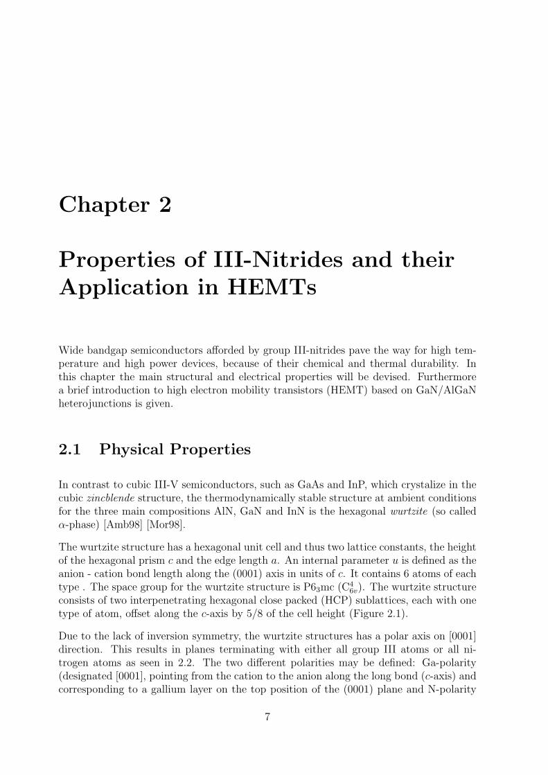
The wurtzite structure has a hexagonal unit cell and thus two lattice constants, the heightof the hexagonal prism c and the edge length a. An internal parameter u is defined as theanion - cation bond length along the (0001) axis in units of c. It contains 6 atoms of eachtype . The space group for the wurtzite structure is P63mc (C4
6v). The wurtzite structureconsists of two interpenetrating hexagonal close packed (HCP) sublattices, each with onetype of atom, offset along the c-axis by 5/8 of the cell height (Figure 2.1).
Due to the lack of inversion symmetry, the wurtzite structures has a polar axis on [0001]direction. This results in planes terminating with either all group III atoms or all ni-trogen atoms as seen in 2.2. The two different polarities may be defined: Ga-polarity(designated [0001], pointing from the cation to the anion along the long bond (c-axis) andcorresponding to a gallium layer on the top position of the (0001) plane and N-polarity
7
8CHAPTER 2. PROPERTIES OF III-NITRIDES AND THEIR APPLICATION IN HEMTS
Figure 2.1: Stick and ball diagram of wurtzitic GaN. According to the ionic radii thesmall spheres represent nitrogen while the big ones represent Gallium.
(designated [0001]) for which nitrogen atoms are on top (Figure 2.2).
It is worth noticing that Ga-faced does not mean Ga-terminated, termination being asurface property connected to the possible reconstructions. The discussed polarities mightbe obtained by using different growth techniques and substrates. It has been reported thathigh quality epitaxial GaN layers deposited by MOVPE on c-plane sapphire substratesgrow in the (0001) direction with Ga-faced surfaces, while MBE growth commonly occursin the (0001) direction, yielding an N-faced GaN layer [Amb98].
The polarity, the non-centrosymmetric structure and the partial ionicity of the chemicalbonding in the group III nitrides are responsible for the polarization effects which appearin the nitride layers. The physical properties of bulk and surface, as there are piezoelectriceffects (described in subsection 2.2.1) depend significantly on the surface polarity [Amb98].
An overview of important values for crystal properties, mechanical and thermal constantsand coefficients is given in table 2.1.
2.2 Electrical Properties of Nitrides
AlN, GaN and InN have different lattice constants, bandgaps and binding energies, be-cause of the different ionic radii. The wurtzitic polytype of GaN, AlN and InN forms a

2.2. ELECTRICAL PROPERTIES OF NITRIDES 9
AlN GaN
Crystal Structure Wurtzite Wurtzite
Lattice Constant a0 [A] 3.112 3.189
Lattice Constant c0 [A] 4.982 5.185
a0/c0 1.6010 1.6259
u0 0.380 0.376
aBohr [A] 5.814 6.04
Static Dielectric Constant εr 8.5 8.9
High Frequency DC εr,HF 4.77 5.35
Energy Gap [eV](Γ Valley) 6.2 3.39
Effective Mass me (Γ Valley) 0.48 0.2
Electron mobility [cm2/Vs] (300K) 135 1000
Hole mobility [cm2/Vs] (300K) 14 30
Saturation velocity [cm/s] 1.4 ×10⁷ 2.5 ×10⁷
Peak velocity [cm/s] 1.7 ×10⁷ 3.1 ×10⁷
Breakdown field [V/cm] >5 ×10⁶
Thermal Conductivity [W/cmK] 2 1.5
ρ [g/cm3] 3.29 6.07
Melting Point TM [K] 3487 2791
Decomposition Point TE [K] 1313 1123
Activation Energy EMN [kJ/mol] 414 379
Spontaneous Polarization PSP [C/m2] -0.081 -0.029
Piezoelectric Constants:
e14 [C/m2] 0.92 0.375
e15 [C/m2] -0.58/-0.48 -0.3/-0.33/-0.22
e31 [C/m2] -0.48/-0.60/-0.58 -0.49/-0.36/-0.33/-0.22
e33 [C/m2] 1.46/1.55 0.73/1/0.65/0.44
Piezoelectric Coefficients:
ε11 9.0 9.5
ε33 10.7 10.4
Elastic constants: exp. cal. exp. cal.
C11 345 396 374 367
C12 125 137 106 135
C13 120 108 70 103
C33 395 373 379 405
C44 118 116 101 95
Table 2.1: Crystal properties of GaN and AlN [Edg94] [Fou03].

10CHAPTER 2. PROPERTIES OF III-NITRIDES AND THEIR APPLICATION IN HEMTS
Figure 2.2: Different polarities (Ga- and N faced) of wurtzite GaN [Amb98].
continuous alloy system (AlGaN, InGaN and InAlN) whose direct bandgaps ranges from0.7 eV for InN and 3.4 eV for GaN to 6.2 eV for AlN. Figure 2.3 displays the bandgapsversus the lattice constant.
Control of the electrical properties of group III nitrides remains the foremost obstaclehindering device efforts.
2.2.1 Spontaneous and Piezoelectric Polarization
Polarization related properties, such as spontaneous and piezoelectric polarization, areimportant for device applications. The electric field caused by polarization influences theshape of the band edges and the carrier distribution of heterostructure interfaces.
Pyroelectric materials exhibit polarization without an external electric field such as thespontaneous polarization in wurtzitic group III nitrides. For a crystal to exhibit spon-taneous polarization it has to have a certain symmetry. Of the 32 point groups, whichdescribe all crystalline systems, 11 are centrosymmetric, i.e. they contain an inversioncenter. In those crystals polar properties are not present, because there is no preferreddirection. Ten of the initial 32 groups have a polar axis, which means they can displayspontaneous polarization.
The wurtzite structure of the group III-nitrides is one of them. The origin of spontaneous

2.2. ELECTRICAL PROPERTIES OF NITRIDES 11
Figure 2.3: Bandgaps of important binary semiconductors.
polarization lies in the ionic or dipole character of the metal nitrogen bond and is alwaysoriented along the crystal c-axis. The direction of the polarization (up or down the c-axis)can be controlled by controlling the polarity of the crystal. Spontaneous polarization canhave significant influence on carrier concentration as well as band edge profiles, since aspontaneous polarization is connected with a surface charge. The polarization strength isdependent on the alloy composition and in general increases from GaN over InN to AlNand depends on the ionic character of the metal nitrogen bond (dipole character). More-over every pyroelectric material is piezoelectric. In theory the strain-induced piezoelectricpolarization in III-nitrides can equal the value of the spontaneous polarization. Sponta-neous PSp and piezoelectric polarization PPe along the c-axis add up to the macroscopicpolarization P :
P = PSp + PPe (2.1)
The sign of the spontaneous polarization is determined by the polarity and is oppositeto the [0001] for metal-face layers. The piezoelectric polarization along the c-axis can becalculated by using the piezoelectric coefficients1 e33 and e13 as
PPe3 = e33ε3 + e31(ε1 + ε2) (2.2)
1The calculated values of the piezoelectric constants in GaN, InN, and AlN are up to ten times largerthan in GaAs based crystals and the sign is opposite to other III-V compounds.

12CHAPTER 2. PROPERTIES OF III-NITRIDES AND THEIR APPLICATION IN HEMTS
Figure 2.4: Sum of the microscopic dipoles, resulting in a spontaneous polarization 6= 0in the wurtzite structure (right) and = 0 in the zincblende (left).
where ε3 = (c− c0)/c0 is the strain along the c-axis, ε1 = ε2 = (a− a0)/a0 is the isotropicin-plain strain, a0 and c0 are the equilibrium values of the lattice parameters.
For a hexagonal structure, the relation between the lattice constants is given by
c− c0
c0
= −2C13
C33
a− a0
a0
(2.3)
where C13 and C33 are the elastic constants (table 2.1 ).
Using equations 2.2 and 2.3 the amount of piezoelectric polarization in the direction ofthe c-axis can be determined by
PPe3 = 2a− a0
a0
(e31 − e33
C13
C33
)(2.4)
The macroscopic polarization results in an electric field:
E = − P
εMaterialε0
(2.5)
where ε0 is the dielectric constant of vacuum and εmaterial is the relativ dielectric constantof the employed material.
For AlxGa1−xN alloys the piezo polarization equals
(e31 − e33
C13
C33
)< 0 (2.6)

2.2. ELECTRICAL PROPERTIES OF NITRIDES 13
and is valid over the whole range (x) of compositions. Therefore from Eq. (2.4) thepiezoelectric polarization is negative for tensile and positive for compressive strained Al-GaN films respectively. As a consequence, the orientation of the piezoelectric polarizationis parallel to the spontaneous polarization for tensile strain and antiparallel in case ofcompressively strained AlGaN layers.
Summarizing, polarization itself and gradients in polarization at interfaces and surfacesof AlGaN/GaN heterostructures induce fixed sheet charges, which in turn cause strongelectric fields inside every heterostructure. In the nitrides the electric field can reach astrength of 3 · 106V/cm and therefore enhance electron or hole accumulation (dependingon the polarity of the material) at AlGaN/GaN interfaces.
2.2.2 HEMT-Structures Based on AlGaN/GaN Heterojunctions
The High Electron Mobility Transistor (HEMT) has emerged as a promising candidate formicrowave power amplification. HEMTs are an integral part of a new generation of groupIII nitride transistors formed between semiconductors of different compositions and bandgaps. These devices offer advantages for instance in microwave and high speed digitalintegrated circuit (IC) applications but most of all as high power devices.
HEMT Heterostructures
The unique feature of the HEMT is channel formation from carriers accumulated along aheterojunction [Sze81, Hei01]. Whatever the physical origin of the carrier accumulation,the carriers have high mobility due to their separation from their source region and theirlocation in a region absent of impurity scattering. Where carriers accumulate a so calledtwo-dimensional electron gas (2DEG) is formed. Usually the origin of the carrier is ajunction between a heavily doped high bandgap and a lightly doped low bandgap region.In HEMTs based on AlGaN/GaN structures, this carrier accumulation is mainly due topolarization charges developed along the heterojunction in the high bandgap AlGaN side.A heterostructure as described above is shown in figure 2.5.
In inset (a) the Fermi levels EF of the two semiconductors do not coincide. At a realheterostructure in thermodynamic equilibrium, this will lead to a bending of the bands,until the structure will have just one common Fermi level (inset (b)). The heterostructureresults in the formation of a discontinuity in the conductance (EC) and valence (EV ) bandat the heterojunction. A triangular quantum well emerges, filled with electrons diffusingfrom semiconductor II and thus the strongly localized 2DEG develops. The term 2DEGrefers to the condition in which electrons have quantized energy levels in one spatialdirection but are free to move in the other two directions, parallel to the interface. Whilefigure 2.5 is valid for all compound semiconductors for group III nitrides also polarization

14CHAPTER 2. PROPERTIES OF III-NITRIDES AND THEIR APPLICATION IN HEMTS
Figure 2.5: Band diagram of the heterostructure formed by lightly n-doped narrow gapsemiconductor I and heavily n-doped wide gap semiconductor II divided one from another(a) and together in thermodynamical equilibrium [Iba99].
effects have to be taken into account.
AlGaN/GaN HEMTs
The carrier accumulation in the quantum well in the AlGaN/GaN heterostructure iscaused by the sum of spontaneous and piezoelectric polarization in the strained2 AlGaNlayer and the spontaneous polarization in the GaN layer. At the heterojunction thepolarization induced sheet charge is positive, thus free electrons will compensate thischarge resulting in the formation of a 2DEG. Since polarization effects depend on theAl-content, higher carrier concentrations can be induced with higher Al amounts in thesolid. For the Ga-face polarity the induced sheet charge is found to be in the AlGaNlayer near the interface (see figure 2.6 a) and therefore the 2DEG is formed in the GaNlayer. For the N-face polarity the polarization has the opposite direction what results inthe formation of the 2DEG in the GaN close to the top interface (figure 2.6 b) [Amb00].
The reason why the AlGaN/GaN heterostructure has been so intensively studied for thelast years is the fact, that the polarization in the layer system is large enough to form a2DEG with high sheet carrier concentrations without the necessity of a doped layer in thestructure.
Due to these material properties applications at elevated temperature (HEMT operationat 750C have been shown [Dau98]) are possible and in comparison with GaAs etc., higherbreakdown voltages, high saturated electron drift velocities and much higher thermal and
2The piezoelectric polarization, present solely in the thin AlGaN layer, originates from the tensilestrain imposed on the AlGaN layer due to the GaN layer underneath.

2.2. ELECTRICAL PROPERTIES OF NITRIDES 15
Figure 2.6: Polarisation induced charge in a Ga-faced (a) and N-faced (b) AlGaN/GaNheterostructure
chemical stability are achieved. For the AlGaN/GaN system simulations have predicteda high peak electron velocity of 2.7 · 105m/s at electric fields of 105V/cm. A mobilityof µe ≈ 2000cm2/V s has been calculated for the 2DEG in the GaN channel at roomtemperature and a sheet carrier concentration of n ≈ 1013cm−2. Together, these materialproperties yield the capability of about ten times as much microwave power density inW/mm channel periphery [Eas02].
In order to grow a HEMT with such sophisticated features several requirements on growthhave to be fulfilled:
1. homogenous layer characteristics
2. Semi-insulating GaN layers to avoid any parallel conductivity to the channel layerand to ensure high HEMT performance at high frequency;
3. good structural quality with low dislocation densities for high amplification by highchannel conductivity at high frequencies.
4. A smooth, defect free surface, important for the growth of sharp interfaces and flatsurfaces as well as for device processing;
5. Tight alloy composition and thickness control in the heterostructure
6. Maximization of the sheet conductivity µ × ns, thus maximizing both the sheetcharge density ns, necessitating the maximization of the spontaneous and piezoelec-tric polarizations with the Al mole fraction and the electron mobility µ requiringthe minimization of scattering centers due to dislocations, interface roughness andalloy disordering at the heterojunction.

16CHAPTER 2. PROPERTIES OF III-NITRIDES AND THEIR APPLICATION IN HEMTS
For device applications an intermediate Al content of about 30 % seems most promising,typically resulting in a sheet carrier density of 1 ×1013cm−2 and a 2DEG mobility of1200 to 1500 cm2/V s at 300K for an AlGaN layer thickness of 30 nm grown on 2 µmsemi-insulating GaN. Usually the sheet carrier density increases with Al content in theAlGaN layer. The mobility of the 2DEG though, decreases with increasing Al-content.Following the model of Zhang and Singh [Zha99], the higher the sheet carrier density andthe sheet charge, the closer the centroid of the 2DEG density is to the interface, and themore the electron transport is affected by the surface roughness. Hence, 30 % contentis assumed to represent an optimum composition. Heterostructure growth is completedwith the deposition of a GaN cap layer.
Electron Transport in AlGaN/GaN
The formation of a 2DEG without intentional doping in AlGaN/GaN heterostructuresoffers a novel phenomena that must be taken into account when determining the transportproperties in the channel. However, in comparison to AlGaAs/GaAs 2DEGs, where themobility is limited by Coulomb scattering induced by remote ionized donors [Smo99,Hir86], the electron mobilities in AlGaN/GaN heterostructures are still lower. A shortreview of scattering events will be given:
Ionized Impurities The separation of electrons from their donors due to the polariza-tion charges reduces the scattering and improves the electron mobility. Therefore scat-tering due to ionized impurities is solely caused by the background doping concentrationthat is usually in the order of 1016cm-3.
Alloy Scattering Alloy disorder scattering originates from the randomly varying alloypotential in the barrier. In AlGaAs/GaAs heterostructures this scattering effect is neg-ligible but in AlGaN/GaN heterostructures, the combination of the large electron mass,the high sheet carrier concentration, and the large alloy potential make this scatteringstrong.
Phonons The phonon scattering limits the mobility in the 2DEG in the range of temper-atures above 80K. The transport is affected by potential acoustic phonons, piezoelectricacoustic phonons, and polar optical phonons [Nag80].
Dislocations Due to the lattice mismatch between substrate and film, GaN layers con-tain typically 108 to 1010 cm-2 of dislocations. Thus changes in the periodicity of the latticelead to local potential changes and so to scattering events. Some threading dislocationsform acceptor like states and act as coulomb scattering centers.

2.2. ELECTRICAL PROPERTIES OF NITRIDES 17
Charged Surface Donors In an undoped heterostructure such as AlGaN/GaN thequestion arises where free electrons originate from. A possible source of electrons seemsto be surface donor states[Amb99], since the mentioned background carrier concentrationis not high enough to produce such a sheet carrier density in the 2DEG. The surface donorstates will form a source of scattering [Riz00] since they diminish the polarization inducedsheet charge and transport scattering occurs similar to a delta-doped remote donor layer.
Interface Roughness Interface roughness scattering limits electronic transport of highdensity 2DEG’s ( 1013cm−3), because the 2DEG shifts closer to the interface as the sheetcarrier concentration increases.
Thus, the electron transport properties of the 2DEG are limited by small angle scatteringfor low sheet carrier concentrations and by large angle scattering for high sheet carrierconcentrations. Dependence of the 2DEG mobility on the temperature and scatteringmechanisms is shown in figure 2.7.
Figure 2.7: Dependence of the 2DEG mobility on the temperature and scattering mech-anisms for AlGaN/GaN heterostructures [Jen01].

18CHAPTER 2. PROPERTIES OF III-NITRIDES AND THEIR APPLICATION IN HEMTS

Chapter 3
Principles of MOVPE GaN Growth
Usually, the production of compound semiconductor based devices requires the growth ofhigh quality epitaxial layers (low defect and impurity levels, precise thickness of the lay-ers close to the monolayer scale, abrupt transitions in composition and sharp interfaces).Metal-organic vapor phase epitaxy1(MOVPE) has been developed in the 1960’s by Man-asevit et al. [Man69], MOVPE, also known as metal-organic chemical vapor deposition(MOCVD), is a deposition method in which a thin solid film is synthesized by the chemicalreaction of molecules from the gaseous phase on a heated surface. CVD processes are veryversatile and suitable for the deposition of both semiconductor materials and coatings. Inthis work MOVPE has been used to grow (Al)GaN films on sapphire substrates. Thesefilms can be produced from several microns down to a thickness on the atomic layer scale,which is important in order to produce atomically sharp heterointerfaces e.g. for HEMTapplications.
In the following the MOVPE process for III-V semiconductors is briefly introduced andthe governing fundamentals are emphasized. Subsequently MOVPE will be discussed withparticular interest in GaN growth.
3.1 MOVPE Process
Among different deposition methods employed for obtaining epitaxial layers such as va-por phase epitaxy (VPE), liquid phase epitaxy (LPE), molecular beam epitaxy (MBE),hydride vapor phase epitaxy (HVPE), MOVPE is the most versatile and suitable method.The MOVPE has evolved into a leading growth technique for III-V compound semicon-
1The term epitaxy derives from the Greek. Epi, meaning on top or onto and taxis which translatesto ordering. Therefore epitaxy denotes the controlled growth of a substance on a single crystalline base,the substrate.
19

20 CHAPTER 3. PRINCIPLES OF MOVPE GAN GROWTH
ductor materials, such as GaAs, AlAs, InP and their alloys. Beside the fact that MOVPEmeets all the quality criteria for the epitaxial layers required for device applications, italso possesses the advantage to grow on large area substrates. Due to the developmentsin the area of optoelectronic applications, the MOVPE became the most successful andmature growth technique for group III nitrides based materials. All the breakthroughs inthe MOVPE growth of group III nitrides such as heteroepitaxial growth on mismatchedsubstrates and introduction of a low temperature nucleation layer, achievement of p-typedoping, control of doping level in the nitride layers and the possibility to grow high quality(defined from structural, optical and electrical point of views) GaN, AlGaN and InGaNlayers qualified the method for the growth of GaN based HEMT structures. It is thegrowth method used in this thesis and its basic principles will be discussed in the nextsections.
3.1.1 General Considerations
MOVPE is a non-equilibrium growth technique which is based on the vapor transport ofthe precursor molecules, i.e. for group III-V based compounds, group III alkyls (denotedR3M where R is an organic radical, typically CH3 or C2H5 and M is a metal from groupIII, Al, Ga or In) and binary hydrogen compounds of group V (denoted EH3 where Eis an nonmetal from Group V, N, P or As) and their subsequent reactions on a heatedsubstrate resulting in epitaxial growth of a thin solid film. In a simplistic manner, whichneglects the complexity of the MOVPE process, a general reaction can be written asfollows:
R3M(g) + EH3 (g) −→ ME(s) + 3RH(g) (3.1)
The precursors are transported by an accurately metered flow of carrier gas (usually highlypure H2 and/or N2) into a reaction chamber. The carrier gas passes through the group IIIsources2 to saturate with vapor from the source and carry a certain amount of materialinto the reactor. Because of the high vapor pressure the group V precursor solely flowsby pressure difference.
The MOVPE process is very complex and consists of a number of reactions involvingboth homogeneous and heterogeneous reactions of the group III and group V sourcemolecules as well as growth related surface processes such as adsorption/desorption ofthe chemical species and surface migration. The carrier gas will transport the sourcemolecules from the reactor inlet to the heated zone of the reactor where they will undergogas phase reactions, typically decomposition reactions (in the nitride growth case evenadduct formation reactions). The resulting species diffuse due to concentration gradients
2Alkyls of group III elements are usually in liquid form contained in so called ”bubblers”, which areheld in thermostats with a controlled temperature and thus posses a well defined vapor pressure.

3.1. MOVPE PROCESS 21
Figure 3.1: Process steps in CVD reactions
in the gas phase to the substrate surface where they are adsorbed at a vacant site. Atthis point, the species can either desorb or react with other surface species (or simplydecompose), then diffuse along the surface before the final incorporation reactions takeplace and the resulting product is incorporated into the film forming a new bond. Thegaseous byproducts that form desorb from the sample surface and diffuse in the carriergas away from the deposition zone towards the reactor exhaust. The basic processes inMOVPE are displayed in figure 3.1.
The MOVPE growth process consists of many parallel and series reaction steps occurringsimultaneously. For series reactions, the slowest step controls the overall reaction rate.For parallel reactions, the overall reaction rate is the sum of the individual reaction rates,hence the fastest reaction controls the overall reaction rate. For such a complex system,the most important elementary steps determining the overall reaction rate is controlled byan interplay between the three components: thermodynamics, kinetics and hydrodynamics(also including mass transport)[Hol96, Har03, Str99].
• The thermodynamics of growth, which describe the driving force for the overallgrowth process by indicating in which direction the reactions will proceed and pre-dicting the solid stoichiometry, as depicted in section 3.1.2.
• The kinetics of growth, shown in section 3.1.3, define the rates at which the possiblegas phase and surface reactions occur.
• The hydrodynamics (section 3.1.4) of the growth process controls not only the masstransport of the molecules in the gas phase, but also the temperature distribution,the velocity profile and total pressure in the reactor.

22 CHAPTER 3. PRINCIPLES OF MOVPE GAN GROWTH
Examining the crystal growth mechanisms it is apparent that a major parameter in CVDgrowth is the deposition temperature. As MOVPE is an exothermic process, the growthrate can be expected to be a complicated function of the temperature according to theArrhenius equation:
k = A exp (−Ea/RT ) (3.2)
where k is the rate constant, A is the pre-exponential factor, Ea is the activation energy,R is the gas constant and T is the absolute temperature. Qualitatively, three growthtemperature regimes [Sha75] can be established from a plot imaging the growth rateversus reciprocal temperature (Fig. 3.2):
Figure 3.2: Typical Arrhenius plot of a CVD deposition process
• kinetically limited regime: At low temperatures the growth is determined (limited)by the reaction rates at the substrate surface. The growth rate increases exponen-tially with the reciprocal temperature.
• mass transport limited regime: at intermediate temperatures the chemical kineticsbecomes faster, and the mass transport (gas diffusion to and away from the surface)is the rate limiting step. The growth rate becomes independent of the substratetemperature. Hydrodynamics influence the layer growth.
• thermodynamically limited regime: at high temperatures the thermodynamic equi-librium shifts to educt formation and hence the growth rate decreases. Also alter-native processes such as depletion of reactants must be considered.

3.1. MOVPE PROCESS 23
For each growth regime there are also other factors which may influence the overall growthrate besides temperature. In the kinetically limited case the surface plays an importantrole. When the mass transport limits the overall growth rate, parameters such as totalflow, flow velocity and reactor pressure must be taken into account. For the thermody-namically limited regime where growth rates decrease due to possible depletion routes(adducts formation, wall deposits), parameters such as reactor geometry, including gasinlet design and time residence may influence considerably the growth.
All these parameters define together the optimal parameter window for a growth processUsually the mass transport limited growth regime is favored, since variations in tempera-ture will not affect the epilayer thickness. However, an analysis of the three componentswhich govern the MOVPE process can provide a better understanding. Hence, in thenext subsections few generalities about thermodynamics, kinetics and hydrodynamics foran MOVPE growth process will be discussed.
3.1.2 Thermodynamics
In CVD, growth is simply a phase transition from the gaseous to the solid phase. Thebasic goal of thermodynamics as applied to epitaxy, is to define the relationship betweenthe compositions of the phases in an equilibrium system at constant temperature andpressure and hence thermodynamics determine the maximum growth rate for all growthprocesses. The driving force for deposition is the striving of the whole system towardsequilibrium [Pie92]. It is therefore useful to know the equilibrium conditions. The Gibbsfree energy function G per mole - also called free enthalpy - provides the true measure ofchemical affinity under conditions of constant temperature and pressure. A system willbe in equilibrium when G is at a minimum [Car94]. The free energy change of a chemicalreaction can be described as
∆Gr = Gproducts −Greactants (3.3)
When the free enthalpy change is zero, there is no net work obtainable. The system isin a state of equilibrium. If the free energy change is positive for a reaction, net workmust be put into the system to effect the reaction, otherwise the reaction cannot takeplace. If the free energy change is negative, the reaction can proceed spontaneously withaccomplishment of net work. Therefore ∆Gr is called the driving force of the reaction3.
For the calculation of the free energy of the reaction mixture, ∆Gr, first the standard freeenergies of formation for the pure reactants and the pure products are employed, givingthe standard reaction free energy, ∆Gr
0 :
3The partial derivative of the free energy ∂G∂ni
with respect to the number of moles n per component i,ni, is known as the chemical potential µi. The chemical potential denotes the required amount of energyfor the phase transition.

24 CHAPTER 3. PRINCIPLES OF MOVPE GAN GROWTH
∆G0r =
∑n∆G0
f (products)−∑
n∆G0f (reactants) (3.4)
where n denotes the stoichiometric coefficients in the chemical equation. While ∆Gr0 is
the difference in molar free energy between the pure products and the pure reactants intheir standard states (for a temperature T and a pressure of 1 atm), ∆Gr refers to anychosen, fixed composition of the reaction mixture. Thus, the value of ∆Gr varies with thecomposition of the reaction mixture. If the reaction mixture contains relatively more re-actants than it would have at equilibrium, then ∆Gr at that composition will be negative,and the system will have the tendency to form more products. For a higher proportionof products than at equilibrium, then ∆Gr will be positive and the reverse reaction, theformation of the reactants, will be spontaneous. At an equilibrium composition of thereaction mixture, ∆Gr = 0 and there is no tendency for the reaction to occur in eitherdirection.
The dependence of ∆Gr on the composition of the reaction mixture can be written as
∆Gr = ∆G0r + RT ln Q (3.5)
where Q is the reaction quotient and R is the gas constant (8.31451 kJ/K·mol). Thereaction quotient is defined in the same way as the equilibrium constant, K. If K isthe ratio of the concentrations (or partial pressures) of the products to those for thereactants, each raised to a power equal to its stoichiometric coefficient in the balancedchemical equation, the reaction quotient defines the same ratio but at any stage of thereaction. Q is expressed in terms of partial pressures, pi (where pi = xiPT , xi being themolar fraction of species i and PT the total pressure) for any gases or ai, activity of speciesi (ai = xiγi, where γi is a non-ideality factor called also activity coefficient).
At equilibrium, ∆Gr = 0, therefore the left-hand term of Eq. 3.5 is equal to 0 and Q =K, the equilibrium constant for the reaction and the equation becomes
∆G0r = −RT ln K (3.6)
This is the link between the equilibrium constant and the standard reaction free energy forany change, physical or chemical Jon00. The value of ∆ Gr
0 gives us information aboutthe yield of the desired reaction at the equilibrium conditions for the reaction mixture.Moreover, from all the tabulated thermodynamic data, phase diagrams of the system inequilibrium state can be constructed, helping to determine the energetically favorablephases as a function of experimental variables (temperature, composition).
A disequilibrium situation is intentionally created by supersaturation of the reactantsthat drives the system to produce the solid desired. This is the driving force for epitaxy.

3.1. MOVPE PROCESS 25
The maximum amount that can be produced is simply the amount that would establishequilibrium and is, thus, fundamentally limited by thermodynamics.
3.1.3 Kinetics
Thermodynamics define the equilibrium conditions but cannot give information on thecourse of a reaction. The kinetics of growth gives more insight on the reaction paths. InMOVPE homogeneous (gas phase) and well as heterogenous reactions (reactions betweengas and sample surface) take place. Where homogeneous reactions have been extensivelystudied by mass spectroscopic techniques, the investigation of the heterogeneous reactionsis still deficient because of lack of experimental tools needed for the measurement of theprocesses at the growing surface. Stringfellow [Str01] notes that ”the least understoodaspect of the entire MOVPE growth process is probably the array of surface reactions andphysical phenomena occurring at the solid/vapor interface during growth”. The difficultiesarise from the fact that both homogeneous and heterogeneous reactions occur simultane-ously, involving several precursors and their intermediates, apart from inhomogeneities intemperature and so forth. Also, reaction mechanism will be affected by so-called ”systemeffects” such as system pressure, reactor geometry and flow conditions. In this context anuniversally valid reaction mechanism for the same growth process in different reactors ishardly conceivable. To this end numerical simulations and process modelling are usefulto understand possible growth pathways together with the transport phenomena in thereactor. As a result, kinetics will here be described with a rather simplistic approach.
For a simple bimolecular reaction with reactants A and B which form the product P , theequilibrium constant K can be written as [Moo78]:
K =k1
k−1=
[P ]
[A][B](3.7)
here k1 and k−1 are the reaction rate constants of the reaction in forward (towards theproduct) and reverse direction. Each reaction rate constant is not dependent on theconcentration of the participating species but is dependent on the temperature accordingto the equation of Arrhenius (3.2)[Ben68, Ben82]:
The difference in activation energy for both reactions Ea,1 and Ea,−1 is equal to:
∆Hr = Ea,1 − Ea,−1 (3.8)
with the reaction enthalpy ∆Hr. The schematics of the formation heat as a function ofthe distance along the reaction path for a simple bimolecular reaction is shown in figure3.3.

26 CHAPTER 3. PRINCIPLES OF MOVPE GAN GROWTH
Figure 3.3: Schematic of the formation heat as a function of the distance along the reactionpath.
For a homogeneous reaction (gas phase reaction) the rate constant k1 can be resolvedas [Str99]:
k1 = PAPBπd2
AB
σAB
√8RT
πµAB
·NA · e−Ea/RT , (3.9)
where PA and PB are the probabilities that a collision between molecules A and B willproceed to reactants (basically depending on orientation factors), dAB is the distancebetween the centers of mass of A and B in the collision complex, σAB is the symmetrynumber for the pair ( 1 for A 6= B, and 2 for A = B), and µAB is the reduced molecularweight (MAMB/(MA + MB)) and NA is Avogadro’s number.
The heterogeneous reactions at the sample surface dominate the overall process. Thesurface has been thought to consist of atomically flat regions separated by steps, whichcan be visualized by atomic force microscopy. In this mode growth occurs by propagationof steps as well as by the formation and propagation of two- and three-dimensional islands.The physical procedure occurring on the surface during growth is depicted in figure 3.4. Asimple model for the interaction at the surface is presented by the Langmuir adsorption.Providing that adsorption and desorption in a stationary state are equal, the surfacecoverage Θ can be expressed by the Langmuir isotherm:
Θi =Kpi
1 + Kpi
(3.10)

3.1. MOVPE PROCESS 27
Figure 3.4: Adatom motion and preferred adsorption at kinks and islands.
K is the equilibrium constant at the surface, here also the adsorption constant and pi thepartial pressure in the vapor of species i. Since this chemisorption process is exothermicthe value of K and hence the surface coverage decreases with increasing temperature.Thus, the reaction rate is proportional to Θ. Assuming that the reaction would be bi-molecular for the III-V semiconductor growth process, the reaction rate rg is proportionalto the coverage of anion and cation species
rg = k1ΘAΘB (3.11)
It should be mentioned that the Langmuir model is too simplistic to describe the actualadsorption of gas molecules on the surface. It has to be taken into account that theadsorbed atoms are known to diffuse to the lowest energy position of the surface beforebeing incorporated into the growing film. Thus, imperfections such as screw dislocations,stacking faults and so forth, may be preferred sites. Other effects due to impuritiescollected on the surface (surfactant effects) also disturb ideal growth.
It was shown that the chemistry of the CVD process is quite complicated since a numberof homogeneous and heterogeneous chemical reactions take place. However the slowestreaction is most important since it will determine the growth rate of the film and istherefore often mainly accounted for in the modelling of the growth process.
3.1.4 Hydrodynamics and Mass Transport
The hydrodynamics are the last fundamental component which describe the overall MOVPEprocess. Transport phenomena (fluid flow, heat transfer and mass transport) finally gov-

28 CHAPTER 3. PRINCIPLES OF MOVPE GAN GROWTH
ern the access of the reactive species to the sample surface and influence the degree ofgas phase reactions taking place before deposition. The knowledge of the phenomena canbe obtained by modelling the growth process [Kle95]. To this end conditions are put intocalculation which are defined by the CVD experiment. The constraints are the processproperties such as reactor geometry, total flow, reactor pressure and substrate temperatureand thermodynamic properties belonging to the reactants and products (this presupposesthat the chemical model of deposition is known) and their partial pressures. In this wayit becomes possible to determine the temperature distribution in the gas phase, the flowprofiles and the distribution of the important chemical species for growth.
CVD Model Equations
Modelling can be used to find a set of start parameters in the case of a growth processdeveloped for a new material system or a new reactor type. In case of a well knownmaterial system, modelling can help find the optimal operating conditions in order toachieve significant growth rates of high quality layers and spatial uniformity of the layerthickness over large-area substrates. However, modelling cannot totally replace the exper-iments. Information from both experiment and modelling are needed to develop a betterunderstanding of the growth process.
The physical treatment of the hydrodynamic aspects in the growth of III-V semiconduc-tors is governed by the simultaneous solution of non-linear, coupled, partial differentialequations for the mass transport, the homogenous and heterogenous kinetics and heattransfer. The transport phenomena are described through mass, momentum and energyconservation [Bir60].
Conservation of mass:
∂
∂tρi = −∇ · (ρi~v +~ji) = −∇ · ~ni (3.12)
The total mass flux ~n from equation (3.12) is the sum of convective and diffusive fluxes.Where ρ is the mass density, i denotes the species, ~v the average mass velocity and ~j thediffusive flux .
Navier-Stokes equation (conservation of momentum):
∂
∂tρ~v = −[∇ · ρ~v~v +
∏] +
∑i
ρi~gi (3.13)
With∏
as the pressure tensor and ~gi as sum of all external forces, equation (3.13) statesthat any momentum change results from convective flow, internal pressure, viscous forcesand external forces such as gravity.
3.1. MOVPE PROCESS 29
Conservation of energy:
∂
∂tρ(E +
1
2υ2) = −∇ · ρ(E +
1
2υ2)v + ~q + [
∏·v]+
∑i
(~ni · ~gi) (3.14)
From the first law of thermodynamics the rate of gain in energy is principally formedfrom convection, conduction (q is the conductive heat flux), the energy dissipation due tocompression and friction, and external forces.
To specify the system it is assumed that the ideal gas law pV = nRT is applicable sinceprecursor and product partial pressures are low. The diffusive flux ~ji to the substratesurface in equation (3.12) combines ordinary Fickian diffusion (driven by concentrationgradients) and thermodiffusion, or Soret diffusion (driven by thermal gradients).
~ji = ~jci + ~jT
i (3.15)
Simplified the flux of the growth limiting species i can be described as [Ric86]
~ji =Di
kT∇pi +
αiDi
kTpi∇T, (3.16)
where Di is the diffusivity, αi is the thermodiffusion factor and k Boltzmann’s constant.
Thermodiffusion usually has a weak effect on the overall diffusive flux, however, it plays arole in MOVPE processes, since the steep temperature gradient in a reactor is in a severalhundred degrees Celsius range. In a nonisothermal reactor the gas is suddenly heatedby the susceptor. The resulting change in density by virtue of gas expansion, gives riseto buoyancy driven convection (natural convection). The thermodiffusion results in thetransport of heavy molecules (in respect to the gas mixture, eg. heavy metalorganics)into cooler regimes opposed to the concentration driven flux. This depletion of the groupIII compounds in the region close to the substrate results in a reduction of the growthrates by 10 - 20% relative to the growth rate achievable in the absence of thermal diffusion[Jen94].
Characteristic Parameters
The basic transport processes are characterized by dimensionless parameter combinationsthat arise from the scaling of the governing transport equations (3.12),(3.13) and (3.14):
The Knudsen number Kn denotes the mean free path λ between collisions for a gasmolecule relative to the characteristic length L. In a horizontal reactor with a rectangularprofile (height h, width w) L can be calculated by use of the hydraulic diameter. Thus,Kn is small for MOVPE reactors.
Kn =λ
L< 0.01 with L = 4
hw
2(w + h)(3.17)

30 CHAPTER 3. PRINCIPLES OF MOVPE GAN GROWTH
The continuum description in equation (3.12),(3.13) and (3.14) is then appropriate, oth-erwise molecules would not undergo gas phase reactions, since they are rarely subject togas phase collisions.
The dynamical behaviour of the reactant gas can be characterized by the Reynolds number.The Reynolds number Re is the relation between kinetic energy and frictional loss
Re =vL
%, (3.18)
where % = ηρ
stands for the kinematic viscosity, defined as ratio of viscosity η and densityρ. Re gives information whether a flow is laminar or turbulent. In case of an isother-mal liner an empirical value of Re > 2300 has been determined above which the flowbecomes chaotic. The transport regime will be dependent on the nature of the carrier gasemployed (%)in the MOVPE growth process. Giling calculated the Reynolds number for4 different carrier gases (H2, He, N2, Ar). He found that the Reynolds number dependson temperature, as a consequence of the variation of the density and viscosity of eachgas with temperature and that for N2 and Ar, at high flow rates, a turbulent regime canbe obtained. Also, for He or H2, at high flow rates, a so called ”entrance effect” can beobserved, which means that the gas flow and temperature profiles are not fully developedand turbulent zones can appear inside of the reactor. However, Re is typically low forconventional MOVPE reactors. In the setup used in this work the Reynolds number is atleast one order of magnitude lower than necessary for the tip over to turbulent flow.
The Rayleigh number Ra serves as a measure of the strength of natural convection inthe system, therefore characterizing the thermal behaviour of the gas flow. Ra gives therelation between buoyancy force and viscous force
Ra =αgcph
3ρ2∆T
ηκ, (3.19)
where α is the thermal expansion coefficient, cp is the specific heat of gas, h is the freeheight of top wall above substrate, ∆T = Thot − Tcold, κ is the thermal conductivityof gas, and g is the gravitational constant. When heated gas is beneath cold gas, forexample in a MOVPE reactor due to the heated susceptor and cold walls, a driving forcefor natural convection exists. With no forced convection, the transition from stagnationto convection occurs for values Ra > 1707. The Ra number for several temperaturesfor H2 and N2 were calculated by [Gil86a]. For normal geometries and temperatures noconvection is predicted for H2, but N2 is expected to be highly convective. Of course ifthe gas encounters an obstacle such as a tilted heated susceptor or if the reactor heightis too large, natural convection can result even in H2. Temperature gradients are theprimary cause of density variation in CVD systems, since the reactants are often usedin such low concentrations that the depletion of reactants by film growth is incapable ofcreating significant density variations in the fluid.

3.1. MOVPE PROCESS 31
Figure 3.5: Schematic diagram of the Rayleigh number versus the Reynolds number,classifying the different flow behavior expected in horizontal CVD reactors [Jen93].
Flow Phenomena in Horizontal Reactor Systems
The aforementioned critical values give a first impression of transport phenomena, but forreal MOVPE reactors (in our case horizontal), a mixed convection mechanism is respon-sible for the transport. Density gradients in reduced and atmospheric pressure reactorsare caused primarily by temperature gradients and thus may produce buoyancy drivenflows that superimpose on the forced flow entering the reactor. This results in mixedconvection transport and hence has significant effects on film thickness and uniformity.In this situation, the flow dynamics will be affected by each detail of the reactor geometry(dead spaces, obstacles or angles between the internal surfaces larger than 10) and flowrecirculation cells, roll cells or turbulent(vortex) motions can be observed. Figure 3.5shows the flow regions in a horizontal geometry based on the Rayleigh-Benard analysis.
Above a critical value Racr two dimensional convection cells, so called longitudinal rolls,develop downstream of the entrance region. The direction of rotation depends on thewall thermal boundary condition, as well as the inlet conditions. Jensen [Jen93] foundout that for an aspect ratio of 2 for the reactor cross-section and insulated side wallsthe rolls rotate inwardly, thus increasing deposition in a midplane. For cold side walls,where flow rotates outwardly deposition increases near the walls and thus decreasing ina midplane. As the roll pattern develops, the downward flow in the reactor center causeslateral nonuniformity in growth rate.
The hydrodynamics approach of the MOVPE growth process demonstrates the complexity

32 CHAPTER 3. PRINCIPLES OF MOVPE GAN GROWTH
of the flow phenomena in an MOVPE reactor. Consequently, most deposition character-istics are reactor dependent. The ”manufacturing uniformity” of semiconductor layers isregulated by the reactor geometry coupled with the fluid dynamics and heat and masstransfer. This makes the translation of experimental data for one reactor to another re-actor type and also the scale-up of reactors very uncertain. As a result of this complexityand despite their disadvantages (time consuming, high costs), trial-and-error methods arestill important in developing new MOVPE growth processes in these circumstances.
3.1.5 Influence of Carrier Gases
The carrier gas plays a decisive role in MOVPE. It transports the group III metalorganicand the group V source compounds into the heated zone of the reactor where decompo-sition processes take place to form the desired highly pure materials. The gas phase (i.e.the reaction medium) in which the chemicals partly decompose mostly consists of carriergas (around 70− 95%) 4. This has several consequences for growth:
• The hydrodynamical properties of the carrier gas such as density, viscosity, heatconductance and specific heat capacity determine the flow velocity- and tempera-ture distribution profiles in the reactor chamber. Therefore the transport and theresidence time of the growth species in the gasphase is significantly influenced.
• Through their respective masses carrier gas molecules initiate reactions of the growthspecies in the gasphase when acting as collision partners. Besides the number ofcollisions the impulse transmission is of importance for activation.
• The carrier gas itself might be product of one of the many reaction paths, thusreaction rates are determined by the carrier gas partial pressure.
• An influence of the carrier gas on surface reaction, absorbtion and desorption is alsoconceivable
Since we employed hydrogen and nitrogen (as well as arbitrary mixtures of both gases) asthe carrier gas in our reactor system, some fundamental properties of these are reviewedhere. These characteristics have a significant influence not only on hydrodynamics buton the gasphase reactions taking place in the reactor. The ratio for several propertiesbetween the two applied carrier gases hydrogen and nitrogen is given as
ρN2
ρH2
= 14 Density (3.20)
4lesser amounts of carrier gas in nitride growth than for classical III-V’s, see section 3.3)

3.2. SAPPHIRE AS SUBSTRATE FOR (AL)GAN GROWTH 33
ηN2
ηH2
= 2.5 Viscosity (3.21)
λN2
λH2
= 0.15 thermal conductivity (3.22)
cpN2
cpH2
= 0.08 specific heat capacity (3.23)
These differences have several consequences in growth:
For instance, the greater mass of N2 relative to H2 transmits higher kinetic energies toits collision partner, which in turn leads to a higher decomposition of the precursors.
Lower thermal conductivity of N2 in comparison to H2 helps to achieve a uniform tem-perature distribution on the substrate surface.
The diffusion constant of reactive species in nitrogen is lower than that for hydrogen whichcan account for lower growth rates.
Especially for nitrogen flows in a high temperature ambient (i.e high Rayleigh numbersas seen in equation 3.19) the existence of complex flow structures were observed by Giling[Gil86b]. Namely the presence of a region of colder gas (so called cold finger) penetratingfrom the inlet into the deposition zone. This cold finger arises from radiative heating ofthe top wall and the subsequent heat transfer to the incoming gas. Hence, if the flow rateis low and the thermal conductivity is high, heat is conducted sufficiently fast relativeto convection (3.19), so that there are no large temperature gradients from susceptor tothe reactor top wall. However, if the gas velocity is fast and/or a gas with lower thermalconductivity (e.g. N2) is used a thermal boundary layer develops along the top wall.
Furthermore N2 is a nonexplosive gas, leading to a safer overall MOVPE process.
3.2 Sapphire as Substrate for (Al)GaN growth
While for GaAs and InP the existence of large area substrates makes homoepitaxial growthpossible, for GaN this option is not available. The high dissociation pressures and meltingtemperatures are the main obstacles in obtaining large group III nitride single crystals,which can serve as substrates for homoepitaxial growth. Therefore single crystalline GaNfilms have been grown heteroepitaxially on several substrates, which match more or lessclosely to its lattice constants. Also different coefficients of thermal expansion betweensubstrate and nitrides cause residual stress upon cooling, which leads to additional struc-tural defects. There is no ideal or particularly suitable substrate available in that matter.
However, providing the thickness h of the epitaxially grown film is sufficiently small apseudomorphic layer can be grown. The structure of a mismatched layer is shown in figure
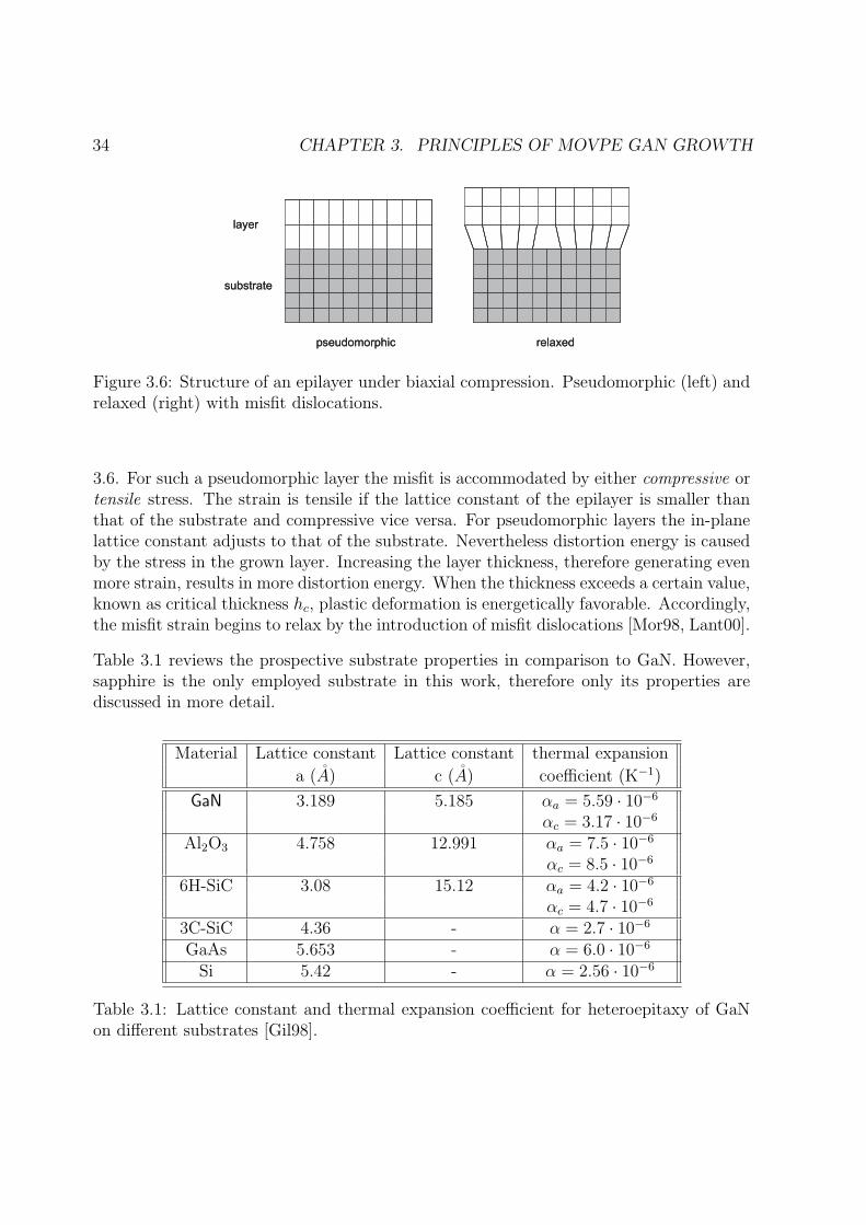
34 CHAPTER 3. PRINCIPLES OF MOVPE GAN GROWTH
Figure 3.6: Structure of an epilayer under biaxial compression. Pseudomorphic (left) andrelaxed (right) with misfit dislocations.
3.6. For such a pseudomorphic layer the misfit is accommodated by either compressive ortensile stress. The strain is tensile if the lattice constant of the epilayer is smaller thanthat of the substrate and compressive vice versa. For pseudomorphic layers the in-planelattice constant adjusts to that of the substrate. Nevertheless distortion energy is causedby the stress in the grown layer. Increasing the layer thickness, therefore generating evenmore strain, results in more distortion energy. When the thickness exceeds a certain value,known as critical thickness hc, plastic deformation is energetically favorable. Accordingly,the misfit strain begins to relax by the introduction of misfit dislocations [Mor98, Lant00].
Table 3.1 reviews the prospective substrate properties in comparison to GaN. However,sapphire is the only employed substrate in this work, therefore only its properties arediscussed in more detail.
Material Lattice constant Lattice constant thermal expansion
a (A) c (A) coefficient (K−1)
GaN 3.189 5.185 αa = 5.59 · 10−6
αc = 3.17 · 10−6
Al2O3 4.758 12.991 αa = 7.5 · 10−6
αc = 8.5 · 10−6
6H-SiC 3.08 15.12 αa = 4.2 · 10−6
αc = 4.7 · 10−6
3C-SiC 4.36 - α = 2.7 · 10−6
GaAs 5.653 - α = 6.0 · 10−6
Si 5.42 - α = 2.56 · 10−6
Table 3.1: Lattice constant and thermal expansion coefficient for heteroepitaxy of GaNon different substrates [Gil98].

3.2. SAPPHIRE AS SUBSTRATE FOR (AL)GAN GROWTH 35
Figure 3.7: Rhombohedral structure and surface planes of the sapphire substrate.
Sapphire Al2O3
Sapphire is the most extensively used substrate for growth of the group III nitrides andGaN in particular. Large area good quality crystals of sapphire are available at low cost.They are transparent, stable at high temperatures, and the growth technology of GaN onsapphire has reached a quite sophisticated level.
GaN can be deposited on one of the four planes of the corundum structure of sapphire,as there is the basal, c-plane (0001), a-plane (1120), r-plane (1102) and m-plane (1010).The latter two are technologically not important due to the obtained low film quality.Figure 3.7 demonstrates the planes and their respective hkl-values.
The lattice mismatch between basal GaN and sapphire plane (both c-plane) can be cal-culated using ∆a = (alayer - asubstrate)/asubstrate, where asubstrate is the effective lattice pa-rameter of the substrate in the epitaxial plane. This mismatch leads to high dislocationdensities (1010 cm−2). Through a variety of techniques, such as low-temperature (LT) AlNor GaN nucleation layers [Ama86, Nak91], multiple intervening LT layers [Ama98], epi-taxial lateral overgrowth [Bea01] and pendeoepitaxy [Zhe99] GaN layers with dislocationdensities as low as 107 cm−2 have been produced. However, these defects have a numberof effects on the layer characteristics. The electrical properties of the material and devicesmade from the material are altered, since defects lower sheet charge carriers concentra-tions, reduce the charge carrier mobility and thermal conductivity in heterostructure fieldeffect transistors [Liu02]. Yet, defects are unavoidable and thus precise control of defecttypes and densities is a prerequisite for high quality GaN growth with respect to HEMT

36 CHAPTER 3. PRINCIPLES OF MOVPE GAN GROWTH
application.
In this work all GaN films were grown on the c-plane, as it is the most common depositiondirection.
3.3 MOVPE III-nitride Growth
The growth of group III nitrides is carried out by introducing a laminar flow of alkylsof the group III elements, such as trimethyl-gallium TMGa), and hydrides or hydrogencompounds of the group V elements, e.g. ammonia (NH3) into the reactor. The reactoritself consists of a quartz tube that contains a substrate. The substrate is situated on asilicon-carbide coated graphite susceptor heated by a radio frequency coil.
Neglecting the reactions of the precursors with the carrier gas, the net reaction betweenTMGa and NH3 taking place during growth of GaN can be indicated as:
(CH3)3Ga + NH3 → GaN + 3CH4 (3.24)
In general, the supply of group III sources is lower than that of group V sources. For onething, this is because of inferior decomposition of the group V molecules in comparison tothe group III, since NH3 is thermally very stable. Even at the growth temperature usedfor HT growth only a few percent of ammonia is decomposed. On the other hand, moregroup V elements desorb from the substrate surface due to their volatility. Thus, highammonia flows stabilize the stoichiometry of the growing layer.
However, decomposition and adduct formation of the source materials occurs in the gasphase even before film growth on the susceptor proceeds. In order to suppress thesereactions caused by gas phase mixing a separation plate (see chapter 4) is introduced intothe reactor, right in between the inlets of group III and V sources. Formation of adductsand so forth would lead to untimely depletion of source materials in the gas phase andhence to reduced growth rates. Using the separation plate, mixing takes place right beforethe heated susceptor.
Besides the aforementioned growth affecting parameters even the carrier gas has an dis-tinct effect on growth. Obviously hydrodynamical properties of the carrier gas changethe transport but at the elevated temperatures, where GaN growth takes place, hydrogendecomposes and influences the growth chemistry in the gasphase and at the surface level,for example by etching the layer. This is a particularly useful effect in the early stages ofheteroepitaxial growth, e.g. during the so-called annealing step, where single islands formthat coalesce later on. In contrast, when growing InGaN/GaN Multi-Quantum-Wells ni-trogen is used as the carrier gas in order to increase the indium incorporation rate, whengrowing the active regions. Thus, in literature there have been many reports how H2 or
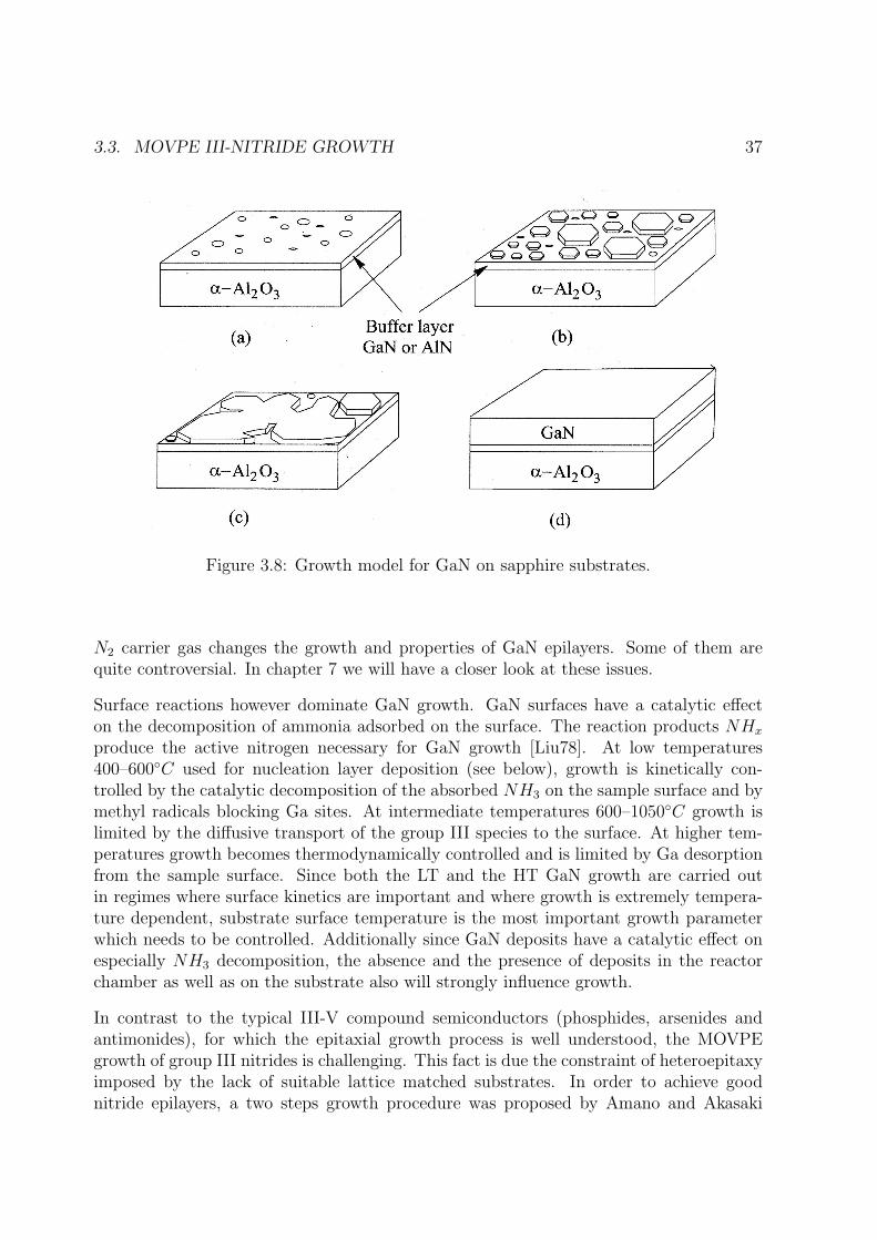
3.3. MOVPE III-NITRIDE GROWTH 37
Figure 3.8: Growth model for GaN on sapphire substrates.
N2 carrier gas changes the growth and properties of GaN epilayers. Some of them arequite controversial. In chapter 7 we will have a closer look at these issues.
Surface reactions however dominate GaN growth. GaN surfaces have a catalytic effecton the decomposition of ammonia adsorbed on the surface. The reaction products NHx
produce the active nitrogen necessary for GaN growth [Liu78]. At low temperatures400–600C used for nucleation layer deposition (see below), growth is kinetically con-trolled by the catalytic decomposition of the absorbed NH3 on the sample surface and bymethyl radicals blocking Ga sites. At intermediate temperatures 600–1050C growth islimited by the diffusive transport of the group III species to the surface. At higher tem-peratures growth becomes thermodynamically controlled and is limited by Ga desorptionfrom the sample surface. Since both the LT and the HT GaN growth are carried outin regimes where surface kinetics are important and where growth is extremely tempera-ture dependent, substrate surface temperature is the most important growth parameterwhich needs to be controlled. Additionally since GaN deposits have a catalytic effect onespecially NH3 decomposition, the absence and the presence of deposits in the reactorchamber as well as on the substrate also will strongly influence growth.
In contrast to the typical III-V compound semiconductors (phosphides, arsenides andantimonides), for which the epitaxial growth process is well understood, the MOVPEgrowth of group III nitrides is challenging. This fact is due the constraint of heteroepitaxyimposed by the lack of suitable lattice matched substrates. In order to achieve goodnitride epilayers, a two steps growth procedure was proposed by Amano and Akasaki

38 CHAPTER 3. PRINCIPLES OF MOVPE GAN GROWTH
[Ama86, Aka89] (Figure 3.8).
In the first step, a GaN nucleation layer is deposited on the substrate at low temperatures(400-600C for sapphire), followed by annealing. Then the main epilayer is grown inthe second step at a higher temperature (usually > 1000C). The nucleation layer mustact as a template between the substrate and the main epilayer. First, the sapphire iscovered with GaN nuclei, randomly distributed which furthermore will develop duringthe annealing step and finally will coalesce in the first part of the high temperature step,allowing the growth of a smooth nitride epilayer with improved structural and electricalproperties. This development of morphology can conveniently be monitored by means ofin-situ reflectometry as introduced in chapter 4.
3.3.1 Modelling of GaN Growth
The principal characteristics of the inverted and conventional inlet growth processes werestudied and compared using modelling. The modelling was performed by the Semicon-ductor Technology Research GmbH in Erlangen. The mathematical model is based on thesolution of the 2D/3D Navier-Stokes conservation equations describing flow, heat transfer,and multi-component diffusion of the gaseous mixture inside the reactor [Bir60], takinginto account the specific reactor geometry, the inlet design and the presence of wall de-posits and particles. However, numerical simulation can only be performed for the hightemperature deposition regime.
The chemical growth process is modelled starting from the following reaction equations.The products of TMGa decomposition are MMGa and atomic gallium. Gas-phase chem-ical reactions include two-step pyrolysis of the initial metal-organic precursor TMGa aspresented in (3.25) and (3.26).
TMGa −→ MMGa + 2CH3 (3.25)
MMGa −→ Ga + CH3 (3.26)
Fairly high temperatures in the reactor result in intensive TMGa pyrolysis producingMMGa, which, in turn, also decomposes to form atomic gallium which is the speciesproviding the greatest contribution to growth.
Additionally, the set of Gas-phase reactions for GaN growth from TMGa and NH3 usedin the computations is [Mih99]:
Ga(CH3)3 −→ GaCH3 + 2CH3 (3.27)
Ga(CH3)3 + NH3 ←→ Ga(CH3)3 : NH3 (3.28)
3 ·Ga(CH3)3 : NH3 −→ 3 · [Ga(CH3)2NH2]3 + 3CH4 (3.29)

3.3. MOVPE III-NITRIDE GROWTH 39
Figure 3.9: Schematic of the GaN decomposition and reaction pathways. Activation en-ergy (kcal/mol) is shown for each reaction pathway. Here, GaN* and Ga* are adsorptionspecies on the surface. Based on the work of Mihopoulos [Mih99]
3 ·Ga(CH3)3 : NH3 + NH3 −→ 3 · [Ga(CH3)2NH2]3 + 3CH4 + 3NH3 (3.30)
[Ga(CH3)2NH2]3 −→ 3GaN + 6CH4 (3.31)
2GaN(s) −→ 2Ga + N2 (3.32)
The kinetic mechanism of MOVPE gas-phase reactions is based on the work of Mihopoulos[Mih99]. The mechanism consists of six reactions and eight species which are shown inthe above equations. The schematic of the GaN decomposition and reaction pathways isshown in figure 3.9.
To simulate the surface chemistry, a quasi-thermodynamic approach is used. This ap-proach is based on the following assumptions:
• The atoms in the adsorption layer on the surface are nearly in equilibrium with thecrystal bulk. This means that the rates of atomic incorporation into the crystal andof the crystal decomposition (occurring at the step edges) are much higher thantheir net difference (growth rate).
• Kinetic effects occurring at the stage of adsorption/desorption can be accounted forby the sticking/evaporation coefficients of the individual species. Generally, thesecoefficients are dependent on temperature and the partial pressures of the species.

40 CHAPTER 3. PRINCIPLES OF MOVPE GAN GROWTH
A further discussion of hydrodynamic effects is found in section 3.1.4.
Chapter 4
Experimental Setup andCharacterization Methods
In this chapter the setup of the employed MOVPE system as well as the applied methodsfor characterization of the deposited layers are discussed. In particular the reactor itselfis described as well as the in-situ tools (reflectometry and pyrometry) emphasized sincethey represent the main tool to control, investigate and interpret the GaN growth in thiswork.
4.1 The Horizontal MOVPE Reactor (Aix 200 RF-S)
The MOVPE system used for the epitaxial growth of thin GaN films in this work wasdesigned for the deposition at reduced pressures. The main constituents of the equipmentare
• reactants and gas handling system,
• the reactor,
• the vacuum and exhaust system,
• the control unit
A more detailed description of these compounds and their application can be found inseveral publications [Jen94] [Sch03a]. In this work, all GaN growth runs were carried outin an AIX 200/4 RF-S horizontal reactor built by Aixtron.
41
42CHAPTER 4. EXPERIMENTAL SETUP AND CHARACTERIZATION METHODS
Gas Handling System and Sources
The reactant handling system mixes and meters the gases to be used in the reactor unit.According to the requirements the carrier gas for the gaseous sources can be switched be-tween nitrogen (N2) and hydrogen (H2). For the growth of GaN the precursors trimethyl-gallium (TMGa), as gallium source, and ammonia (NH3), as nitrogen source, were used.Furthermore trimethylaluminum (TMAl) as aluminium source as well as n-type (SiH4)dopants are available. By use of mass flow and pressure controllers the total gas flow isaccurately metered and controlled. The metal-organic group III compound and the groupV nitrogen source are fed to the gas inlet in the reactor head via two separate lines (RunMO and Run Hydrides), in order to avoid any reactions between the educts. The gasinlet of the reactor was additionally equipped with valves in order to be able to choosebetween the conventional 1 and the inverted inlet configuration 2(see below). Parallel tothe two main lines that lead into the reactor a third is available that directs the gas flowalongside the reactor, the Vent line. As a result the flows can be stabilized before theyare introduced into the reactor. Both Run and Vent line are pressure-wise controlled inorder to afford equal pressure conditions and hence preventing pressure surge in the eventof switching operation.
The Reactor
The core of the MOVPE system consists of a cylindrical steel mantled, horizontal cold wallreactor. This steel setup was chosen in order to provide us with three optical windows.The whole construction is required to tolerate typical growth conditions for the depositionof high quality GaN with temperatures of 1100 C and above, and at low pressures of 200mbar and below.
The stainless steel reactor has three optical ports (as seen in figure 4.1), through which in-situ reflectometry measurements are accomplished as well as ellipsometry could be carriedout. These ports are constantly rinsed with the carrier gas in order to avoid depositionwith particles from inside the reactor which in turn would hinder in-situ measurementefforts. The reactor contains a quartz liner (which is the actual reaction chamber) with arectangular cross section (13.1 cm × 4.5 cm). The void between liner and steel mantle isconstantly flushed. Thus, the process gas cannot leave the liner.
Within the liner a so called separation plate is installed so as to reduce adduct formationbetween the group III and group V source, as shown in figure 4.2. The carrier gas, loadedwith TMGa and NH3, is transported onto the heated susceptor, where growth takesplace. Usually, the NH3 enriched flow enters the reactor beneath the separation plate,while the MO flow enters from above the separation plate. The inlet configuration may as
1Metalorganic sources through the upper channel, ammonia through the lower channel.2Vice versa to the conventional inlet.
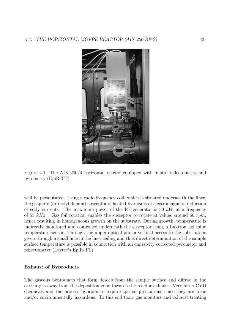
4.1. THE HORIZONTAL MOVPE REACTOR (AIX 200 RF-S) 43
Figure 4.1: The AIX 200/4 horizontal reactor equipped with in-situ reflectometry andpyrometry (EpiR-TT)
well be permutated. Using a radio frequency coil, which is situated underneath the liner,the graphite (or molybdenum) susceptor is heated by means of electromagnetic inductionof eddy currents. The maximum power of the RF-generator is 30 kW at a frequencyof 55 kHz . Gas foil rotation enables the susceptor to rotate at values around 60 rpm,hence resulting in homogeneous growth on the substrate. During growth, temperature isindirectly monitored and controlled underneath the susceptor using a Luxtron lightpipetemperature sensor. Through the upper optical port a vertical access to the substrate isgiven through a small hole in the liner ceiling and thus direct determination of the samplesurface temperature is possible in connection with an emissivity corrected pyrometer andreflectometer (Laytec’s EpiR-TT).
Exhaust of Byproducts
The gaseous byproducts that form desorb from the sample surface and diffuse in thecarrier gas away from the deposition zone towards the reactor exhaust. Very often CVDchemicals and the process byproducts require special precautions since they are toxicand/or environmentally hazardous. To this end toxic gas monitors and exhaust treating
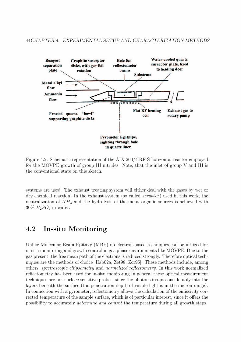
44CHAPTER 4. EXPERIMENTAL SETUP AND CHARACTERIZATION METHODS
Figure 4.2: Schematic representation of the AIX 200/4 RF-S horizontal reactor employedfor the MOVPE growth of group III nitrides. Note, that the inlet of group V and III isthe conventional state on this sketch.
systems are used. The exhaust treating system will either deal with the gases by wet ordry chemical reaction. In the exhaust system (so called scrubber) used in this work, theneutralization of NH3 and the hydrolysis of the metal-organic sources is achieved with30% H2SO4 in water.
4.2 In-situ Monitoring
Unlike Molecular Beam Epitaxy (MBE) no electron-based techniques can be utilized forin-situ monitoring and growth control in gas phase environments like MOVPE. Due to thegas present, the free mean path of the electrons is reduced strongly. Therefore optical tech-niques are the methods of choice [Hab02a, Zet98, Zor95]. These methods include, amongothers, spectroscopic ellipsometry and normalized reflectometry. In this work normalizedreflectometry has been used for in-situ monitoring.In general these optical measurementtechniques are not surface sensitive probes, since the photons irrupt considerably into thelayers beneath the surface (the penetration depth of visible light is in the micron range).In connection with a pyrometer, reflectometry allows the calculation of the emissivity cor-rected temperature of the sample surface, which is of particular interest, since it offers thepossibility to accurately determine and control the temperature during all growth steps.

4.2. IN-SITU MONITORING 45
In the following section the measurement principle and the setup used for in-situ normal-ized reflectometry and emissivity corrected pyrometry will be described.
4.2.1 In-situ Normalized Reflectometry
The plain reflectance signal offers a convenient method of determining growth rates andternary compositions as well an easy tool to monitor growth steps [Hab02b].
XBO-lampdetector
monochromator
beamsplitterAWM
wafer
rotating susceptor
Figure 4.3: Schematic of the in-situ reflectometer as used for measurements on rotatingsamples to detect the reflection [Hab02].
Figure 4.3 is a schematical description of the arrangement. The reflectometer consists ofa xenon lamp which is used as light source with a spectral range of 1.5 eV to 6.0 eV . Nextto the source several filters are installed. Every couple of seconds the source is shadedand a dark signal is measured to determine the background signal. Additionally a bandedge filter can be introduced in front of the xenon lamp in order to suppress light above2 eV . Hence, diffraction maxima of higher order caused by low wavelengths are disabled.Then the light travels via a spherical mirror to a beamsplitter, where it is focused almostperpendicular to the sample surface onto the susceptor. From here it is reflected onto atoggle mirror that compensates the tipping of the susceptor. Finally the reflected intensityis detected. A more accurate description of this arrangement can be found in [Thi02].
Due to the lack of GaN substrates the growth of GaN can only take place on substrates of

46CHAPTER 4. EXPERIMENTAL SETUP AND CHARACTERIZATION METHODS
a different material such as sapphire. Thus it is assumed that a three-phase-model (air/layer/ substrate), describing the optical properties of the layer substrate configuration,can be employed to depict the reflections occurring in the layers during growth. As longas the penetration depth of the light is larger than the thickness of the layer and the layercan be treated as a homogeneous film, the optical properties of all three phases contributeto the reflectance.
The three-phase model can be reduced to a two-phase model3 (only substrate and ambient)by defining an effective dielectric function describing the integral effect of the layer andthe substrate therefore simplifying the reflection occurring during the growth process onmulti layer structures. Using the Fresnel equations the reflectance can be calculated[Bor80]. In the case of perpendicular incidence the reflectivity R equals to
R = |r|2 =Ir
Ii
=E2
r
E2i
=
(n1 − n0
n1 + n0
), (4.1)
where Ir and Er is the reflected light intensity and reflected field component, respectively.Ii and Ei is the incident intensity and the incident field, respectively. Here n is therefractive index of the ambient medium.
Figure 4.4: Schematic diagram illustrating the normalized reflectance. Layer B is nor-malized to the reflectance of layer A [Hab02].
Due to the fact that the actually measured signal is the detector voltage U , some way ofcalibrating this voltage to the sample’s reflectivity R is needed. A normalized reflectanceR/Rref is used here for in-situ measurement, which is the reflectivity of the growing layerdivided by the reflectivity of the substrate. This is illustrated in figure 4.4
If the reflectivity is continuously measured during growth a transient graph, as exhibitedin figure 4.5, is acquired.
3This is also known as the effective media model [Bor80]

4.2. IN-SITU MONITORING 47
Figure 4.5: Typical reflectance transient measured at a wavelength of 600 nm.
By means of the transient growth rates and, where applicable, surface roughness can bedetermined. If λ is the wavelength of the used light and n the refractive index of thelayer, then the maximum of the Fabry-Perot oscillations due to interference, (followingBragg’s relation) of the reflected light can be found at thicknesses d such as
n · d = (m) · λ
2(4.2)
with m > 1 as integer. During growth layer thickness increases constantly so that amaximum of reflection is reached every time (4.2) is fulfilled. Thus the growth rate µgr
can be calculated by using the interval between two of these maxima
µgr =λ
2n∆t(4.3)
The reflectance signal offers not only the opportunity to measure such a crucial parameteras the growth rate, in addition information about the growth process itself can be obtainedas will be discussed in chapter 6

48CHAPTER 4. EXPERIMENTAL SETUP AND CHARACTERIZATION METHODS
4.2.2 Pyrometry
All substances at temperatures above absolute zero emit radiant energy as the resultof the atomic and molecular agitation that is associated with the temperature of thesubstances. The rate of emission per unit area increases with increase in temperature.Accordingly, the temperature of a substance can be measured by means of detectingsuch radiant energy. This thermal radiation is characterized by a spectrum that dependson the temperature T . Pyrometry or radiation thermometry is the determination oftemperature by analyzing this emission spectrum. Depending on the wavelength rangestudied, this procedure is called either optical or infrared pyrometry and is performedwith an instrument called pyrometer. Because of its fast response this method is oftenused in thin film processing. In our experimental setup there are two pyrometers. One isintegral part of the reflectometer setup and the other measures underneath the susceptorvia a lightpipe sensor (compare section 4.1.
Principles of Pyrometry
The pyrometry measurement is based on detection of the incandescence from a surfaceaccording to the Planck equation and Kirchhoff’s law [Pla00, Kir59]. The Planck spectralradiance (L) emitted from a surface of a blackbody in thermal equilibrium at temperatureT is
Lblackbody(λ, T ) =2hc2
0
λ5 exp(hc0/λkT )− 1(4.4)
where λ is the emitted wavelength, h is Planck’s constant, c0 is the speed of light invacuum and k is the Boltzmann’s constant. Figure 4.6 shows the spectral radiance ofblackbody emission for several wavelengths. Hence, determining the surface temperaturefrom a blackbody is a straightforward task.
However, real materials are seldom ideal blackbodies, i.e. bodies that absorb all incidentradiation and at the same time are isotropically diffusive emitters. The optical pyrometermeasures the spectral radiance of a real body Lλ, according to
Lλ(λ, T ) = εLbb (4.5)
where ε is called the spectral directional emissivity. It represents the ratio of the thermalradiation emitted from a real object to that from a blackbody. According to equation 4.5the thermal emission is corrected by the emissivity factor.

4.2. IN-SITU MONITORING 49
Figure 4.6: Spectral radiance of a blackbody from Planck’s radiation law for severaltemperatures.
The emissivity ε depends on the reflectivity (ρ) and transmittance (τ) of the material.Following the radiation balance
ρ + α + τ = 1 (4.6)
and Kirchhoff’s law stating that at thermal equilibrium, the emissivity of a body (orsurface) equals its absorptivity ε = α, we find
ε = 1− ρ− τ (4.7)
For opaque media the transmittance becomes zero, therefore epsilon strongly depends onthe reflectivity.
When pyrometric measurements are made at photon energies higher than the peak ra-diance the high-energy approximation of Planck’s radiation law can be used. Using theWien approximation [for λT < λmaxT ] the inferred temperature from the surface of theobject with the emissivity ε can be determined as
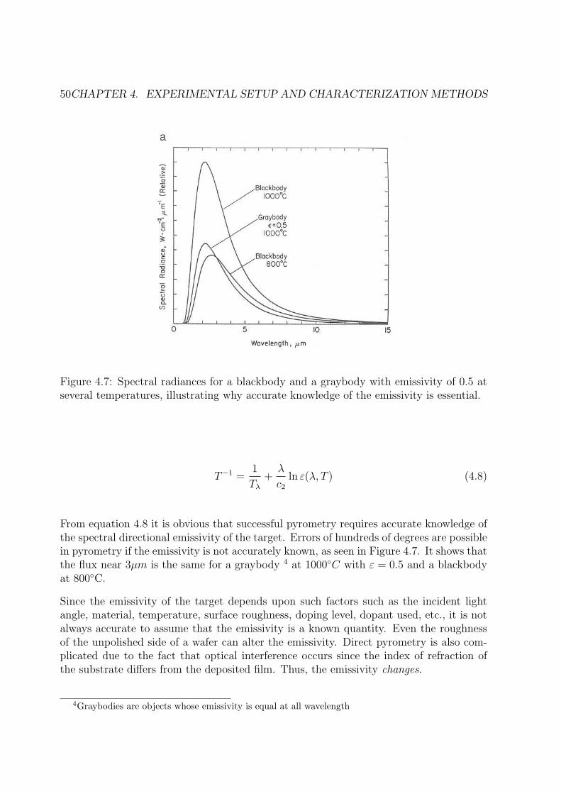
50CHAPTER 4. EXPERIMENTAL SETUP AND CHARACTERIZATION METHODS
Figure 4.7: Spectral radiances for a blackbody and a graybody with emissivity of 0.5 atseveral temperatures, illustrating why accurate knowledge of the emissivity is essential.
T−1 =1
Tλ
+λ
c2
ln ε(λ, T ) (4.8)
From equation 4.8 it is obvious that successful pyrometry requires accurate knowledge ofthe spectral directional emissivity of the target. Errors of hundreds of degrees are possiblein pyrometry if the emissivity is not accurately known, as seen in Figure 4.7. It shows thatthe flux near 3µm is the same for a graybody 4 at 1000C with ε = 0.5 and a blackbodyat 800C.
Since the emissivity of the target depends upon such factors such as the incident lightangle, material, temperature, surface roughness, doping level, dopant used, etc., it is notalways accurate to assume that the emissivity is a known quantity. Even the roughnessof the unpolished side of a wafer can alter the emissivity. Direct pyrometry is also com-plicated due to the fact that optical interference occurs since the index of refraction ofthe substrate differs from the deposited film. Thus, the emissivity changes.
4Graybodies are objects whose emissivity is equal at all wavelength

4.2. IN-SITU MONITORING 51
TS
susceptor
surface temperature
opaque transparent
Twafer
incident light
reflected light
emissivity of wafer emissivity of susceptor
TS
susceptor
surface temperature
opaque transparentopaque transparent
Twafer
incident light
reflected light
emissivity of wafer emissivity of susceptor
Figure 4.8: Pyrometry from opaque wafers such as Si or GaAs is a straightforward taskas seen on the left half. The emissivity (ε) of the substrate surface can be calculated fromthe measured reflectivity. On transparent substrates the pyrometer detects the emissivityof the underlying holder rather than that of the transparent substrate.
Emissivity Corrected Pyrometry
These issues are overcome with emissivity corrected pyrometry (ECP). Simply stated,this in-situ measurement technique requires the combined functionality of a conventionalpyrometer and a reflectometer. The reflectance of the substrate is measured at the samewavelength at which the pyrometer measures the thermal radiance. By using the equation(4.7) 5 the spectral directional emissivity (ε) of the substrate surface can be calculatedfrom the measured spectral directional reflectivity. Now, it is apparent why transparentsubstrates cannot be measured pyrometrically. At the employed detection wavelength(here: 950nm) the optical radiation from the susceptor passes through the transparentsubstrate and the pyrometer cannot distinguish between substrate radiation and susceptorradiation. The second problem is that the substrate emissivity at our detection wavelengthis negligible yielding no usable blackbody radiance. Thus a calibration of the ECP isneeded.
Calibration Methods
Presently, the most effective methods to calibrate real-time emissivity corrected pyrome-ters are procedures based on melting points or phase transitions. To the latter one belongsthe very convenient method based on the Si-Al-eutectic formation at T = 577C. Thisphase transition of a thin Al-layer on Si is accompanied by a sudden roughening of thesurface, which leads to a dramatic loss in reflectance that can be seen with the naked eye,or more conveniently, can be detected by a reflectance sensor. Figure 4.9 shows the re-flectance drop measured at the Ferdinand Braun Institute Berlin (FBH) performed witha LayTec EpiRAS-200 spectrometer that allows combined reflectance anisotropy spec-
5with negligible transmittance (with an opaque susceptor)

52CHAPTER 4. EXPERIMENTAL SETUP AND CHARACTERIZATION METHODS
550 560 570 580 590 600 610 6200.0
0.2
0.4
0.6
0.8
1.0Si/Al-Eutectic (577°C)
0.1°C / s
Rotationflow: 0 sccm
Refl
ecti
on
/arb
.unit
s
T / °C
Figure 4.9: Calibration run based on the Si-Al-eutectic formation at T = 577C wherea sudden roughening of the surface leads to a dramatic loss in reflectance. Experimentconducted at the Ferdinand Braun Institute Berlin in an AIX 200/4
troscopy (RAS) [Asp95] and reflectance (R) measurements between 826nm (1.5 eV) and248nm (5.0 eV). However this method is rather time consuming and yields only one datapoint at 577C. Also, the calibration accuracy could be influenced by Al-layer thickness.
4.3 Ex-situ Characterization Methods
4.3.1 Film Thickness and Homogeneity
As mentioned earlier optical methods such as reflectometry facilitate the actual layerthickness measurement. Using a Bio-Rad RPM2000 system, thickness mappings werecarried out to obtain the thickness distribution of GaN samples. The system can scanwafers up to 1 mm thickness at a resolution of up to 0.1 µm.
Light from the sample is collected by a lens and fed to a spectrometer. The latter measuresa definable wavelength range. These spectra exhibit typical interference effects because ofmultiple beam interference, where the spectral intensity is a function of the film thickness.With respect to the wavelength extrema are found. In principle the thickness d can nowbe calculated by use of equation (4.2). Therefore, if the film’s optical constants are

4.3. EX-SITU CHARACTERIZATION METHODS 53
known the thickness can be determined from the measured reflectivity. The basis of themeasurement method is similar to the already discussed reflectometry.
Furthermore weakly absorbing films and multilayer films can also be evaluated by useof the two phase model as mentioned in subsection 4.2.1, therefore defining an effectivedielectric function which describes the lower layers as an effective substrate.
4.3.2 Differential Interference Contrast Microscopy
Optical microscopy with all its derived types such as phase-contrast microscopy, differ-ential interference-contrast microscopy or fluorescence microscopy is widely applied inphysics, chemistry and biology. For our purpose, i.e. the layer morphology inspection af-ter growth, the differential interference-contrast (DIC) microscopy 6 was employed. Thistechnique is well suited topography evaluation of semiconductor layers and devices, aswell as for locating defects on the surfaces.
Figure 4.10: Schematic of Differential Interference Contrast.
Brightfield illumination is the normal, most even illumination mode for microscopy.A full cone of light is focused by an objective on the sample. The sample is uniformly
6sometime referred to as Nomarski microscopy after the French optics theoretician named GeorgesNomarski.

54CHAPTER 4. EXPERIMENTAL SETUP AND CHARACTERIZATION METHODS
illuminated. The picture observed is the result of differences in reflectivity created bymaterial properties of the sample, e.g. transmission and reflection through surface films,and by the surface contour of the sample.
Interference contrast is a special type of brightfield illumination. Figure 4.10 showsthe apparatus. Differences in height result in laterally different intensities and thereforein image contrast. Etch pits and cracks which are not detectable in brightfield will standout clearly enough to be photographed in interference contrast. The Nomarski techniqueis especially good for observing the topography on semiconductors since it is capable oflocating defects, such as pits, hillocks, cracks and other defects. This is very beneficialfor group III nitride layers grown on sapphire substrates which are almost transparent.
4.3.3 Atomic Force Microscopy
Atomic force microscopy (AFM) provides three-dimensional surface topography at nanome-ter lateral and sub-angstrom vertical resolution on semiconductors and other materials.A sharp tip 7 on the end of a flexible cantilever scans a sample surface, while maintain-ing a constant force. The surface is scanned by a piezoelectric tube that moves the tipin a raster pattern with respect to the sample. The tip-sample interaction is monitoredby reflecting a laser off the back of the cantilever into a split photodiode detector. Bydetecting the difference in the photodetector output voltages, changes in the cantileverdeflection or oscillation amplitude are determined. A more detailed discussion is found in[Bin86, Ste03]
The two most commonly used modes of operation are contact mode and tapping mode.In this work the samples were investigated using the tapping mode. Here the cantileveris oscillating close to its resonance frequency (typically ∼ 300 kHz) and lightly tappingon the surface during the scan. The laser deflection method is used to detect the root-mean-square (rms) amplitude of the cantilever oscillation. A feedback loop maintains aconstant oscillation amplitude by moving the scanner vertically at every x,y data point.Recording this movement forms the topographical image.
For investigation of atomically smooth surfaces, the AFM is very suitable, since the AFMpossesses a very good vertical resolution. It can resolve monoatomic steps on the samplesurface as well as calculate an rms roughness of the surface. Figure 4.11 displays parallelterrace like steps of epitaxially grown GaN.
Surface morphology investigations for the grown GaN and AlxGa1−xN/GaN layers wereperformed by atomic force microscopy (AFM) with a DI Nanoscope IIIa microscope op-erating in tapping mode. The rms roughness of the surface was calculated using the AFMsoftware.
7The tips typically have an end radius of 2 nm to 20 nm, depending on the tip type.

4.3. EX-SITU CHARACTERIZATION METHODS 55
Figure 4.11: A smooth surface revealing terrace like steps of a GaN layer, as seen byAFM.
4.3.4 Photoluminescence Spectroscopy
Photoluminescence Spectroscopy (PL) is a contactless, nondestructive method of probingthe optical properties of materials. Photoluminescence is the emitted radiation from asample as a consequence of light absorption 8. The spectral analysis of this light allowsstatements on (in case of direct semiconductors) the band gap, crystal-quality, strain,impurities and defects. For more detailed information on PL on GaN refer to [Thi02].
It has to be kept in mind that due to the limited penetration depth of light only a certaindepth of the specimen may be analyzed. The main recombination processes (as shown infigure 4.12) for a direct band gap semiconductor are:
• Band Band Transition
• Excitons
• Band Acceptor Transition
• Donor Acceptor Pair Transition
Strain measurements by PL are particularly easy for GaN. GaN layers grown on sapphiresuffer from compressive strain. The band gap increases in case of biaxial in-plane compres-sion compared to fully relaxed GaN. The donor bound exciton (DBX) energy thereforeincreases (from ∼ 3.466 eV ) with increasing compressive strain in the layers.
8During a PL experiment usually a direct band gap semiconductor is excited with light of a higherenergy than the bandgap, ~ωLaser > EGap, usually laser light.

56CHAPTER 4. EXPERIMENTAL SETUP AND CHARACTERIZATION METHODS
Figure 4.12: Recombination processes for a direct band gap semiconductor. (A) BandBand Transition (e, h), (B) Band Acceptor Transition (e, A0), (C) Donor Acceptor PairTransition (D0, A0), (D) Excitons.
The spectra collected in the near band edge range (3.42 to 3.52 eV ) were obtained usingan excitation energy of 50 µW, with a 1200 lines/mm grid.
4.3.5 X-ray diffraction
X-ray diffraction (XRD) is a widely-used technique in materials science, as a highly sen-sitive tool for detailed structural studies.
X-ray diffraction can be explained in simple terms by the ”reflection” of an incident X-raybeam from a stack of parallel equidistant atomic planes. The electrons that surround theatoms, rather than the atomic nuclei themselves, are the entities which physically interactwith the incoming X-ray photons. At each atomic plane a small portion of the beam isreflected. If those reflected beams do not cancel each other by interference, a diffractedbeam can be observed. The condition where the reflected beams interfere positively (addup in phase) to give a strong diffracted beam is given by Bragg’s law (compare equation(4.2)).
The Bragg law may be written as :
nλ = 2dhklsinθB (4.9)
where n is an integral number describing the order of reflection, λ is the wavelength of theX-rays, dhkl is the spacing between the lattice planes and θB is the Bragg angle where amaximum in the diffracted intensity occurs. At other angles there is little or no diffractedintensity, because of negative interference. Since we know λ and we can measure θB, we

4.3. EX-SITU CHARACTERIZATION METHODS 57
can calculate the interplanar spacings. The characteristic set of dhkl spacings generatedin a typical X-ray scan provides a unique ”fingerprint” of the material.
Using adequate incidence angles, various information about the crystal structure, compo-sition or imperfections can be obtained. In this work X-ray diffraction has been used todetermine the crystal quality of GaN layers and qualitatively compare dislocation densi-ties (see Chapter 7). The structural characteristics of the GaN epilayers were evaluatedby X-ray diffraction (XRD), using the symmetric (002) and asymmetric (102) reflection.The full width at half maximum (FWHM) of which are sensitive to all types of threadingdislocations (TDs), such as screw, edge type and mixed TDs, and to pure edge and mixedtypes of TDs, respectively [Hey96].
4.3.6 Rutherford Backscattering Spectroscopy
Rutherford Backscattering Spectroscopy (RBS) analysis is performed by bombarding asample target with a mono-energetic beam of high energy particles, typically He+ ions,with an energy of a few MeV . A fraction of the incident atoms scatters backwards fromheavier atoms in the near surface region of the target material, and is usually detected witha solid state detector that measures their energy. The energy of a backscattered particle isrelated to the depth and mass of the target atom, while the number of backscattered par-ticles detected from any given element is proportional to its concentration. This relationis used to generate a quantitative depth profile of the upper 1 to 2 µm of the sample. Theprimary applications of RBS are the quantitative depth profiling of thin film structuresand their crystallinity
RBS was employed to analyze the obtained AlxGa1−xN/GaN layers. The spectra wereacquired under random incidence (i.e. the angle of incidence does not coincide with alow index direction and channelling does not occur). In these conditions, many sub-surface atomic layers are hit and backscattering occurs from many deeper atoms. Thebackscattering spectrum exhibits a high intensity continuum of scattered energies up to amaximum defined by the surface peak due to scattering on the topmost layer [Iba99]. Fig-ure 4.13 shows an RBS spectrum acquired for an AlxGa1−xN/GaN layer along a randomdirection in order to determine the layer thickness and composition.
The acquired spectrum can be simulated under the assumption of a stoichiometric ratio ofgroup V (N) and group III (Al,Ga) elements, by inserting different relative concentrationsof Ga and Al until the best fit is obtained (see Fig. 4.13). The AlxGa1−xN layer com-position can be determined with an accuracy of ±2 atomic percent for Al. The relativeprecision of the Al level from sample to sample measured in the same RBS analysis isapproximately ±1 atomic percent.

58CHAPTER 4. EXPERIMENTAL SETUP AND CHARACTERIZATION METHODS
Figure 4.13: RBS spectrum of an AlxGa1−xN/GaN layer. The zigzag line is the RBSspectrum acquired in random geometry and the continuous line represents the best fitfrom which the AlxGa1−xN layer composition (35 at% Al, 65 at% Ga) and the thickness(27 nm) were determined.
4.3.7 Contactless Sheet Resistance Measurement
Resistivity is a primary quantity for characterization of semiconductor material. An eddy-current instrument directly measures nondestructively the conductance of a specimen.Values of sheet resistance and resistivity are calculated from the measured conductance,with the resistivity values also requiring a measurement of specimen thickness. Theeffective sheet resistance of a bulk substrate is its bulk resistivity ρ (in Ωcm) divided byits thickness d in cm.
Rs =ρ
d=
RA
ld(4.10)
R is the electrical resistance of a uniform specimen of the material (measured in ohms),l is the length of the specimen (measured in meters) and A is the cross-sectional area ofthe specimen (measured in square meters). LEI Eddy Current systems measure the con-ductivity of a sample by producing an RF magnetic field perpendicular to and throughthe sample. The measurement principle is based on the absorption and dissipation ofthe magnetic field in the sample. The change in energy is measured and thus conduc-tivity calculated. Since the magnetic energy passes through the sample, bulk wafers andmulti-layered wafers can be measured. The bulk specimens may be single crystal or poly-crystalline and of either conductivity type (p or n) in the form of slice wafers (round

4.3. EX-SITU CHARACTERIZATION METHODS 59
or other shape) that are free of diffusions or other conducting layers that are fabricatedthereon, that are free of cracks, voids or other structural discontinuities. The substrateon which the thin film is fabricated should have an effective sheet resistance at least 1000times that of the thin film. LEI systems can measure sheet resistance from below 0.1 Ω/¤to above 3000 Ω/¤. When measured within the proper resistance ranges LEI systemsmeasure these sheet resistances to within +/-3% .
4.3.8 Hall Effect Measurement
Hall effect measurements are commonly used to determine electrical properties of solidssuch as concentration and mobility of charge carriers [Hal79]. The Hall effect is causedby the deflection of moving charged particles (i.e. electrons) by a magnetic field (Lorentzforce). The carriers are accumulated at the edges of the samples resulting in an electricfield which compensates the Lorentz force. By measuring the voltage associated with thisthe carrier concentration can be obtained. For a bar shaped sample with the thickness dthe carrier concentration is given by the following expression,
n = − BI
edVH
(4.11)
where I is the current through the sample, B is the magnetic field, e is the electroniccharge and VH is the measured Hall voltage. When measuring GaN samples, it is worthmentioning that the measured carrier concentration is an effective one (donors minusacceptors), which does not take compensation effects (traps and such) into account. Thesign of the Hall voltage, positive or negative, gives the p- or n-type semiconductor.
The Hall mobility (depending on electron transport as discussed in chapter 2) is obtained,when additionally the resistance R of the sample is measured. Then µ is given by
µ =1
en· l
wd· 1
R, (4.12)
where e is the electronic charge, n is the charge density, l the length, w the width and dthe thickness of the sample.
According to (4.12) for a bar shaped sample the actual dimensions (d, w and length l)of the sample are necessary to determine all parameters. For everyday characterizationpurposes usually arbitrary shaped samples are used. There the so called van der Pauwmethod is applied for the Hall measurements [Pau58]. With this method the mobilityand carrier concentration of arbitrary shaped samples can be determined as long as thereare no holes, nonconducting islands or inclusions (i.e. the sample is simply connected),the ohmic contacts are placed on the periphery (preferably in the corners of the plate)

60CHAPTER 4. EXPERIMENTAL SETUP AND CHARACTERIZATION METHODS
and the contacts are sufficiently small. For detailed discussions of this method please see[Lant00, Ste03].
Hall effect measurements were done at 300 K and 77 K using the van der Pauw configu-ration, to determine the resistivity of the layers as well as the electron mobility and thecarrier concentration, using In balls for ohmic contacts. The In balls were annealed at400C for 3 - 4 minutes in order to achieve ohmic contacts. AlGaN/GaN heterojunctionswere contacted using a procedure in an RTP oven [Ber05].

Chapter 5
Determination of SurfaceTemperature on TransparentSubstrates
Accurate monitoring of growth temperatures is essential during GaN MOVPE growth.The layer qualities, growth rates, abruptness of heterointerfaces and ternary alloy compo-sitions are all dependent on growth temperature. Hence, in-situ measurement and controlof the substrate temperature in nitride MOVPE is crucial for obtaining reproducible layerquality. This chapter deals with temperature measurement on transparent substrates andthe difficulties associated with commonly applied calibration methods. A new method fortemperature calibration by using the in-situ measured band-gap shift of SiC in conjunctionwith real-time emissivity corrected pyrometry for transparent substrates is demonstrated.Eventually limitations of this new method are addressed.
5.1 Standard Measurement Techniques vs. Emissiv-
ity Corrected Pyrometry
For temperature determination thermocouples and pyrometers are the most widely usedtools for measuring and controlling the process temperature, likewise in our system, whichis equipped with a Luxtron light pipe sensor (compare chapter 4). Thermocouples areoften inaccurate because they make no thermal contact with the sample. Due to susceptorand/or wafer rotation the thermocouple is far away from the growing layer. Therefore,the true wafer temperature has an offset to the process control temperature. This offset isnot constant since changes in the susceptor setup or increasing reactor wall coatings andeven different rotation gas flows alter the actual wafer surface temperature [Har04a]andhence, this offset cannot be compensated by calibration. Fig 5.1 demonstrates this effect.
61

62CHAPTER 5. DETERMINATION OF SURFACE TEMPERATURE ON TRANSPARENT SUBSTRATES
As the process temperature is constant the real surface temperature changes drasticallyas a function of the rotation gas flow. All these indicated issues also hold for light-pipe sensors, which pyrometrically sense the temperature indirectly from underneath thesusceptor setup.
0 2000 4000 6000 8000 10000 12000 14000990
995
1000
1005
1010
1088
1089
1090
1091
1092
0
50 sccm 100200
300
400
0 sccm
500sccm
carrier gas: hydrogen
rotation gas: nitrogen
surface Tlight pipe T
tem
pera
ture
[°C]
time [s]
Figure 5.1: Temperature offset between wafer surface and process control temperature asdetermined by ECP and a light pipe pyrometer respectively for increasing rotation flows.
Real-time emissivity corrected direct pyrometry (ECP) [Bob94] of the susceptor and thewafer surface overcomes these problems. However, since optically transparent substratessuch as sapphire or SiC are often employed for GaN MOVPE growth, the measuredsurface temperature represents the susceptor surface temperature and has to be correctedfor the temperature difference between wafer and susceptor. Presently, calibration of real-time emissivity corrected pyrometers is achieved by procedures based on melting pointsor phase transitions [Hab02b] as demonstrated in chapter 4. It will be shown that thisapproach is not always applicable.
5.2 Conventional Calibration Methods
Presently, the most effective methods to calibrate real-time emissivity corrected pyrome-ters are procedures based on melting points or phase transitions as presented in chapter 4.
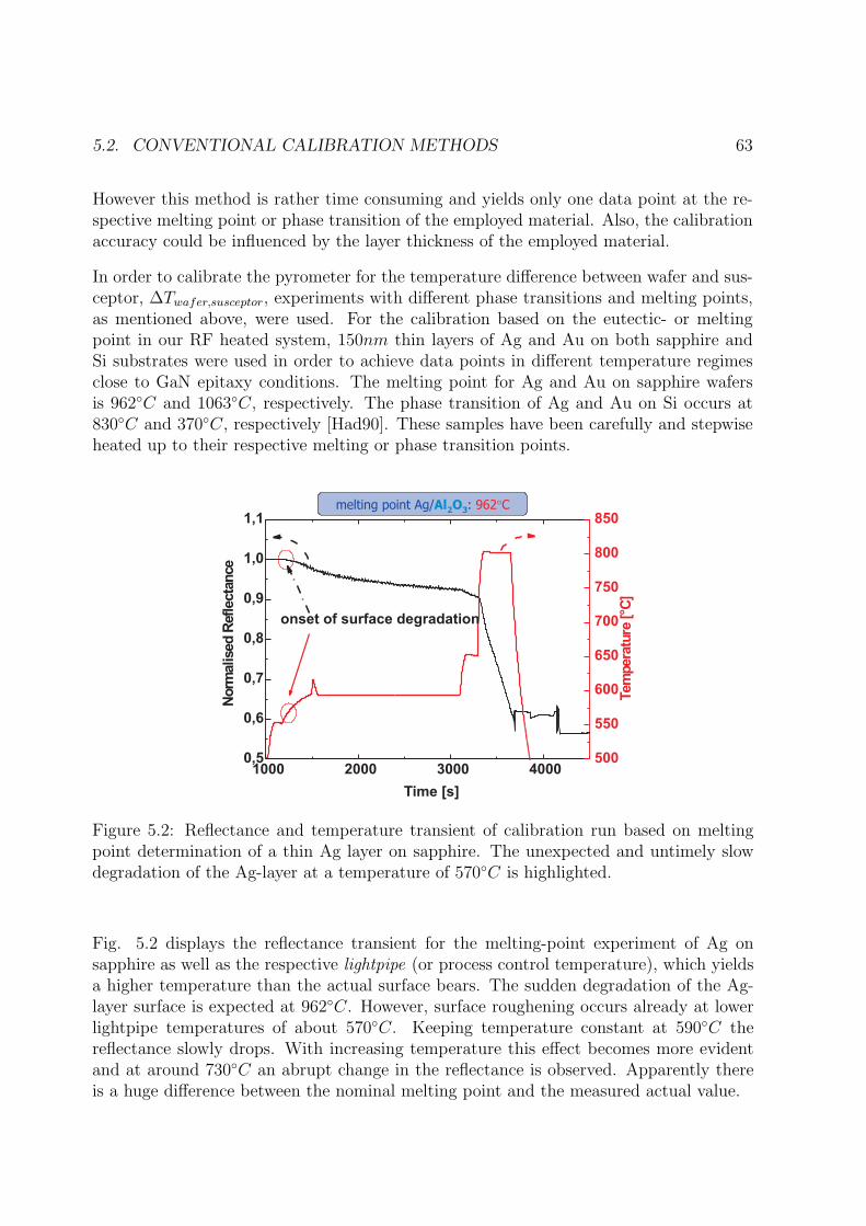
5.2. CONVENTIONAL CALIBRATION METHODS 63
However this method is rather time consuming and yields only one data point at the re-spective melting point or phase transition of the employed material. Also, the calibrationaccuracy could be influenced by the layer thickness of the employed material.
In order to calibrate the pyrometer for the temperature difference between wafer and sus-ceptor, ∆Twafer,susceptor, experiments with different phase transitions and melting points,as mentioned above, were used. For the calibration based on the eutectic- or meltingpoint in our RF heated system, 150nm thin layers of Ag and Au on both sapphire andSi substrates were used in order to achieve data points in different temperature regimesclose to GaN epitaxy conditions. The melting point for Ag and Au on sapphire wafersis 962C and 1063C, respectively. The phase transition of Ag and Au on Si occurs at830C and 370C, respectively [Had90]. These samples have been carefully and stepwiseheated up to their respective melting or phase transition points.
Figure 5.2: Reflectance and temperature transient of calibration run based on meltingpoint determination of a thin Ag layer on sapphire. The unexpected and untimely slowdegradation of the Ag-layer at a temperature of 570C is highlighted.
Fig. 5.2 displays the reflectance transient for the melting-point experiment of Ag onsapphire as well as the respective lightpipe (or process control temperature), which yieldsa higher temperature than the actual surface bears. The sudden degradation of the Ag-layer surface is expected at 962C. However, surface roughening occurs already at lowerlightpipe temperatures of about 570C. Keeping temperature constant at 590C thereflectance slowly drops. With increasing temperature this effect becomes more evidentand at around 730C an abrupt change in the reflectance is observed. Apparently thereis a huge difference between the nominal melting point and the measured actual value.
64CHAPTER 5. DETERMINATION OF SURFACE TEMPERATURE ON TRANSPARENT SUBSTRATES
While many reactors are heated via irradiation of the susceptor with IR lamps our horizon-tal reactor system is inductively heated via a RF-coil situated underneath the susceptorsetup. Thus, the untimely slow degradation of the surface is attributed to inductive heat-ing of the metallic film due to the RF-heating of the susceptor material. Hence, methodsbased on melting points and phase transitions for absolute temperature calibration are notapplicable for our RF-heated system. Another way for absolute temperature calibrationhas to be found.
5.3 New Calibration Approach with SiC Band Tem-
perature Dependence
The band gap of many IV and III–V materials varies strongly with temperature. There-fore, spectral reflectometry holds possibilities for utilizing this shift to reference the sub-strate temperature during MOVPE growth [Tim92, Bal03, Joh93]. To be more precisethe temperature dependent absorption edge is measured which is directly related to thebandgap energy.
The energy bandgap of semiconductors tends to decrease as the temperature is increased.This behavior can be better understood if one considers that the interatomic spacingincreases with the thermal vibrations in the lattice. An increased interatomic spacingdecreases the average potential seen by the electrons in the material, which in turn reducesthe size of the energy bandgap. The temperature dependence of the of the energy bandgaphas been experimentally determined [Var67] yielding the following empirical expressionfor the bandgap Eg as a function of the temperature T
Eg(T ) = Eg(0)− αT 2
T + β(5.1)
where Eg(0), α and β are material dependent fitting parameters. While both empiricaland theoretical equations exist for band gap dependence on temperature for most mate-rials of interest, in practise these equations do not consider doping effects, scattering ormore simply the instrument response. As a result it is much more accurate to generateexperimental calibration curves.
In this thesis a new method for temperature calibration is demonstrated by using thein-situ measured temperature-dependent band-gap shift of SiC in conjunction with real-time emissivity corrected pyrometry. SiC was chosen since its a semiconductor and itsbandgap is in the detection range of our reflectometer (unlike sapphire). It is transparentfor visible light, just as sapphire wafers used throughout this work. Moreover SiC is thesubstrate of choice for many applications in opto- and power electronics for III-nitrides.

5.3. NEW CALIBRATION APPROACH WITH SIC BAND TEMPERATURE DEPENDENCE65
300 400 500 6000.0
0.2
0.4
0.6
0.8
1.0
1.2
1.4
100°C
800°C
refl
ecta
nce/
a.u
wavelength / nm
4 3.5 3 2.5
photon energy / eV
Figure 5.3: Reflection raw signal from SiC (double side polished, undoped) for two tem-peratures.
The temperature-dependent SiC band gap shift measurement were carried out using twoinch, double side polished, 450 µm thick, 6H-SiC substrate, supplied by NovaSiC. Doubleside polished SiC substrates were used to enhance the detected reflectance signal level,since less light is scattered by the rough wafer backside.
The band-gap1 can be determined from the radiation reflected from the susceptor andtransmitted through the substrate. The optical measurements at ForschungszentrumJuelich (FZJ) were performed at 950nm with an EpiR-M-TT optical in-situ sensor hav-ing two separate measurement channels for emissivity corrected pyrometry and high ac-curacy reflectance measurements at a wavelength range from 826 (1.5 eV ) to 248 nm (5.0eV ). These were compared to measurements performed at the Ferdinand Braun InstituteBerlin (FBH) with a LayTec EpiRAS-200 spectrometer that allows combined reflectanceanisotropy spectroscopy (RAS) and reflectance (R) measurements in the same wavelengthrange from 1.5 to 5 eV .
In this set of experiments reflectance spectra with a resolution of 0.01eV were recordedfor a range of true temperatures at FBH and nominal light pipe temperatures at FZJ.The first set of experiments is conducted at FBH. The IR heating system was calibratedby means of phase transition measurements with a non-rotating susceptor in order toexclude cooling effects due to rotation gas flow. The measurement error due to the phasetransition calibration is assumed to be less than ±2K. Thus, the detected temperature
1To be more precise the temperature dependent absorption edge is measured which is directly relatedto the bandgap energy.

66CHAPTER 5. DETERMINATION OF SURFACE TEMPERATURE ON TRANSPARENT SUBSTRATES
2.0 2.5 3.0 3.5 4.00.4
0.5
0.6
0.7
0.8
0.9
1.0
1.1
T up:
100°C
200°C
300°C
400°C
500°C
600°C
700°C
800°C
RSiC
/R
SiC
,R
T
Energy / eV
absorption onset
Figure 5.4: Normalized reflectance spectra referenced to the room temperature spectrumof an undoped double side polished SiC wafer for a range of absolute temperatures. Thestraight lines represent the fit function used to determine the onset of the absorption.
is very close to the absolute temperature.
Looking at the reflectance spectra, the ”band gap” becomes clearly visible as a step inthe reflection signal. Figure 5.3 displays the reflection raw signal from SiC (double sidepolished, undoped) for two temperatures. Superposed is the spectrum of the white lightsource yielding the maximum intensity around 2.65 eV . However, the onset of absorption(”band gap”) is found at around 400 nm (∼ 3.2 eV ) and 470 nm (∼ 2.7 eV ) for wafertemperatures of 100C and 800C respectively.
Fig. 5.4 displays the inferred reflectance spectra from 2.0 to 4.0eV for an unintentionallydoped SiC wafer for a range of temperatures. The spectra are normalized and have beenreferenced to the room temperature spectrum. Thus, the difference in reflectance due tothe different transmission/ absorption is emphasized and the superposed white-light sourcespectrum filtered. These spectra display a sharp falling edge which corresponds to theonset of absorption in the layer. This onset is correlated to the band gap. With increasingsubstrate temperature the position of the falling edge moves to lower energies as the bandgap decreases. It should be noted that even at high temperatures the absorption edge isstill in the visible spectrum range. Using a suitable fit function (straight lines in Fig.5.4)the position of the absorption onset versus the absolute temperature was determined asseen in Fig.5.5. This fit is basically a fermi function with material dependent characteristicreflection values (instrument response) that gives the ”bandgap” energy.
Now, a gauging normal is established since the correlation of the band gap shift (or more
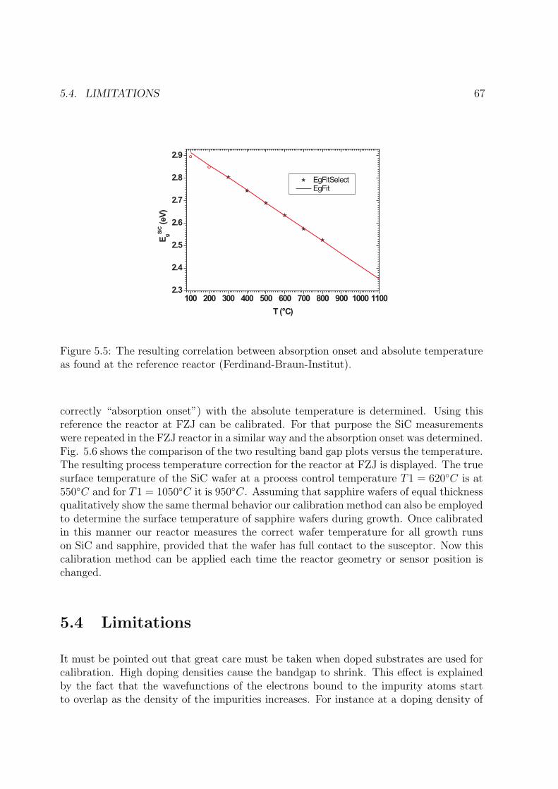
5.4. LIMITATIONS 67
Figure 5.5: The resulting correlation between absorption onset and absolute temperatureas found at the reference reactor (Ferdinand-Braun-Institut).
correctly “absorption onset”) with the absolute temperature is determined. Using thisreference the reactor at FZJ can be calibrated. For that purpose the SiC measurementswere repeated in the FZJ reactor in a similar way and the absorption onset was determined.Fig. 5.6 shows the comparison of the two resulting band gap plots versus the temperature.The resulting process temperature correction for the reactor at FZJ is displayed. The truesurface temperature of the SiC wafer at a process control temperature T1 = 620C is at550C and for T1 = 1050C it is 950C. Assuming that sapphire wafers of equal thicknessqualitatively show the same thermal behavior our calibration method can also be employedto determine the surface temperature of sapphire wafers during growth. Once calibratedin this manner our reactor measures the correct wafer temperature for all growth runson SiC and sapphire, provided that the wafer has full contact to the susceptor. Now thiscalibration method can be applied each time the reactor geometry or sensor position ischanged.
5.4 Limitations
It must be pointed out that great care must be taken when doped substrates are used forcalibration. High doping densities cause the bandgap to shrink. This effect is explainedby the fact that the wavefunctions of the electrons bound to the impurity atoms startto overlap as the density of the impurities increases. For instance at a doping density of

68CHAPTER 5. DETERMINATION OF SURFACE TEMPERATURE ON TRANSPARENT SUBSTRATES
Figure 5.6: Referencing our temperature, empty circles, to the absolute temperature, fullcircles. The true surface temperature of the SiC wafer at a process control temperatureT1=620 C is at 550 C and for T1=1050 C it is 950 C.
1018cm−3, the average distance between two impurities is only 10nm. This overlap forcesthe energies to form an energy band rather than a discreet level. This fact is easily proven.Transmission measurements of non intentionally (< 5E17) and doped SiC (> 1e18) showsignificant changes of the absorption behavior of the substrate. Fig.5.7 demonstrates thenormalized reflectance spectra of an undoped SiC wafer versus two other substrates ofhigher doping concentration. The band edge is strongly broadened by the dopants and/orthe free carriers make the material opaque.
Moreover the ECP system as it is described here cannot account for substrate temperaturedifferences due to wafer bowing effects, that might occur especially for thin substrates. Inour case, where non lattice matched materials (as GaN on sapphire) are grown, a strongconcave wafer bowing might occur. The inhomogeneous contact or distance betweenwafer and susceptor leads to considerable differences in the wafer surface temperature.Combined curvature and ECP measurements give access to this effect [Kro05].
In addition, in this setup pyrometry depends on the reliable measurement of the waferreflection and therefore effects such as wafer wobbling or rough surfaces have to be elim-inated, since they reduce the accuracy of the measurement.
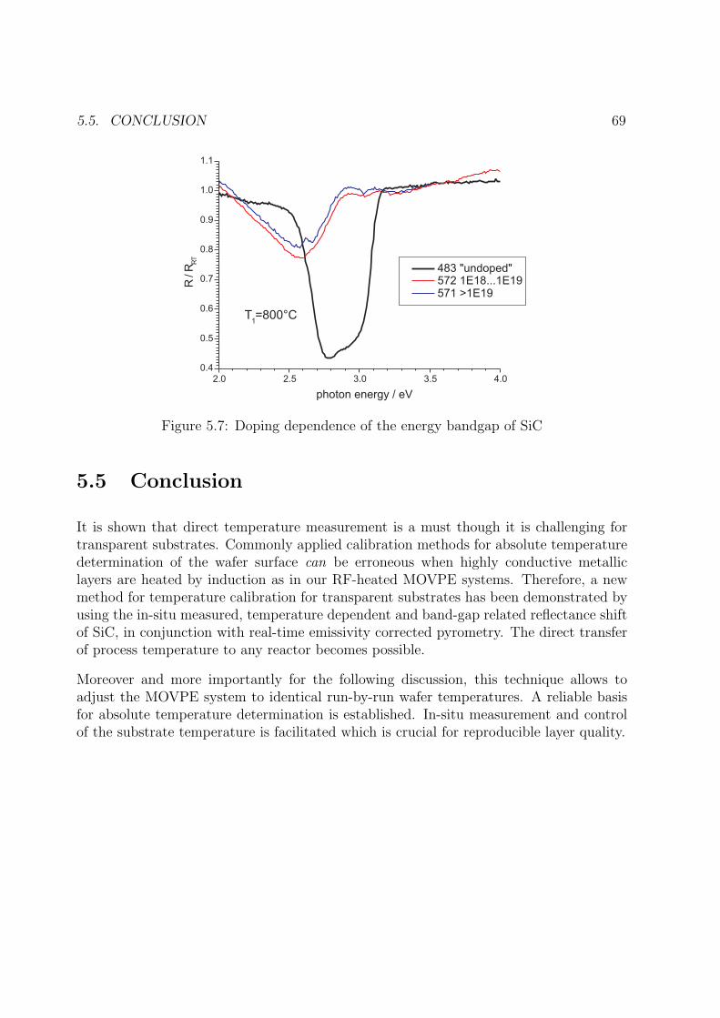
5.5. CONCLUSION 69
Figure 5.7: Doping dependence of the energy bandgap of SiC
5.5 Conclusion
It is shown that direct temperature measurement is a must though it is challenging fortransparent substrates. Commonly applied calibration methods for absolute temperaturedetermination of the wafer surface can be erroneous when highly conductive metalliclayers are heated by induction as in our RF-heated MOVPE systems. Therefore, a newmethod for temperature calibration for transparent substrates has been demonstrated byusing the in-situ measured, temperature dependent and band-gap related reflectance shiftof SiC, in conjunction with real-time emissivity corrected pyrometry. The direct transferof process temperature to any reactor becomes possible.
Moreover and more importantly for the following discussion, this technique allows toadjust the MOVPE system to identical run-by-run wafer temperatures. A reliable basisfor absolute temperature determination is established. In-situ measurement and controlof the substrate temperature is facilitated which is crucial for reproducible layer quality.

70CHAPTER 5. DETERMINATION OF SURFACE TEMPERATURE ON TRANSPARENT SUBSTRATES

Chapter 6
New Growth Approach for GaN
This chapter deals with the development and optimization of a new MOVPE processapproach on sapphire substrates with respect to AlGaN/GaN HEMT application.
Following this goal, the chapter is organized as follows: Beginning with a presentation ofthe applied MOVPE growth process on sapphire substrates the morphological develop-ment of GaN growth is discussed. Moreover, the reproducibility of the AIX 200/4 RF-Ssystem is addressed. The source of irreproducibility will be investigated using the newapproach for temperature determination (chapter 5). Counteractive measures are exam-ined and implemented: A new deposition approach is introduced that takes care to avoidparasitic depositions on the reactor walls. Numerical simulations and growth modellingwill be presented to prove the principal feasibility of the counteractive measures and toestablish a broad comprehension of the epitaxial process. At last the commonly appliedgrowth process is compared to the new one.
6.1 Morphological Development of MOVPE GaN
In the following section the standard MOVPE GaN growth process and the morphologicaldevelopment is discussed. The morphological development during GaN deposition will bemonitored by in situ normalized reflectometry. This in situ method will be applied tooptimize MOVPE of GaN on sapphire.
The high dissociation pressures and melting temperatures are the main obstacles in obtain-ing large group III nitride single crystals, which can serve as substrates for homoepitaxialgrowth. Therefore they are not yet commercially available and other substrates have beenemployed with considerable mismatch to GaN regarding lattice constants, thermal expan-sion and so forth. However, sapphire is the most extensively used. In general the qualityof films grown directly (i.e. without any transition layer) on any plane of sapphire is poor.
71
72 CHAPTER 6. NEW GROWTH APPROACH FOR GAN
To name just a few effects the degradation can be evidenced by XRD measurements (highFWHM values for symmetric and asymmetric rocking curves), morphology investigation(surface contains hillocks), and photoluminescence spectra (considerable yellow emission).In 1983 Yoshida et al. [Yos83] started the deposition of AlN buffer layers prior to thegrowth of GaN. Amano et al. [Ama86] adopted this process to MOVPE growth. Theyintroduced a thin AlN layer, grown on sapphire at lower temperature than the subse-quent GaN layer, in a so-called two-step growth technique. Nakamura [Nak91] suggested1991 that the quality of GaN layers improves if low temperature GaN nucleation layersare used. Hence, with a proper surface preparation and an optimized accommodationbetween substrate and main layer, good quality GaN films can be obtained.
The complexity of the GaN growth process requires a precise and fast control. The in-situ reflectometry method employed during growth is capable of providing information forreal time identification of the growth stages which can be helpful to optimize the growthprocess. The evaluation of the information extracted from the reflectometry transientsallows a faster optimization of the growth parameters which influence the properties ofthe layer. Furthermore, by combining the in-situ with ex-situ characterization methods(such as AFM, HALL or XRD), a better understanding of the GaN growth mechanism onsapphire can be obtained. In order to identify and analyze the GaN growth stages for ourprocess, the in-situ reflectometry method was employed during a standard GaN growthrun. A complete reflectance transient for GaN growth in Fig. 6.1 (black line) is presentedtogether with the AFM pictures which show the morphology at different growth stages.Also, the temperature profile recorded during the entire growth process is presented (greyline).
In our case, GaN growth was performed in an AIXTRON 200/4 RF-S single wafer reactorusing TMGa and NH3 as precursors and H2 or N2 as carrier gas. Although the GaNgrowth MOVPE process is originally called a two-step process, the entire growth processin fact is a succession of more than the two mentioned steps:
Substrate pretreatment:
The sapphire substrate is heated up to above 1000C where desorption takes place. Thisis performed under hydrogen ambient in order to free the substrate of absorbed gaseousmolecules and moreover to chemically clean the substrates by the reaction of carbon toalkanes and oxygen to water. Desorption, as the most common preparation procedureprior to MOVPE growth is reported to anneal the wafer surface and thus to reducethe roughness of the substrate which can present damages from the applied mechanicalpolishing procedure [Cui00].
The exemplary growth transient in figure 6.1 reveals no change in reflection due to thesubstrate pretreatment.

6.1. MORPHOLOGICAL DEVELOPMENT OF MOVPE GAN 73
aa
bb
cc
dd
0 2000 4000 60000.0
0.5
1.0
1.5
2.0
2.5
3.0
3.5
d
c
b
a
Two dimensional
layer-by-layer growth
Fabry-Perot oscillations
Coale
scence
Annealin
g
Nucl
eatio
n
Deso
rptio
n
Time (s)
R/R
Sapphir
e
0
200
400
600
800
1000
1200
Tem
pera
ture
(°C
)
d
c
b
a
Figure 6.1: Typical reflectance transient (black line) and temperature (grey line) recordedduring a standard growth run of GaN on sapphire. AFM insets show the morphology atdifferent stages of growth: Nucleation layer before (a) and after recrystallization (b),during the evolution of island coalescence (c) and the final surface with atomic steps aftercoalescence (d).
Nucleation layer growth:
Following the desorption step the reactor is ramped to a pressure of typically 200 mbarat a temperature of around 500C. At this temperature a thin nucleation layer of about20 to 30nm is grown. The nucleation layer (which acts as buffer or accommodation layerbetween the main GaN film and the substrate) provides the high density of nucleationcenters and, in growth steps following the nucleation, it promotes the lateral growth of themain layer. As a result of the low growth temperature the crystal quality is very poor. Thenucleation layer consists of both small crystallites embedded in amorphous material. The

74 CHAPTER 6. NEW GROWTH APPROACH FOR GAN
thickness of the nucleation represents the most important parameter for the subsequentlygrown main epilayer, in terms of surface morphology, electrical and structural properties[Hir97]. The layer thickness determines the crystallite size after annealing.
Figure 6.1 displays the detected in-situ reflectometry data during growth. Apparently thereflectance increases, due to the higher refractive index of GaN (nGaN ≈ 2.45) in com-parison to sapphire(nsaph ≈ 1.75, compare equation (4.1)). A film covering the substrateis formed and therefore a first Fabry-Perot oscillation is recorded. AFM studies show(Inset (a) in figure 6.1) a very smooth surface, containing very small grains.
Annealing:
Right after the nucleation layer growth the temperature is intentionally slowly ramped upto growth conditions. As the temperature increases the surface is stabilized with NH3.This annealing or recrystallization process turns the amorphous layer into a wurtzitic filmwith preferential orientation (i.e [0001] for c-sapphire) having an improved crystallinity.Also some of the material decomposes and evaporates at high temperatures, thus etchingthe material. During this step the GaN nuclei further develop to islands. The first islandsform from the desorbed (gas-phase) Ga atoms generated during the NL decomposition(evidence for this mechanism is presented in [Kol04]). The most important parameterhere is the annealing time. An extended annealing time will promote the reevaporationof GaN and etch the layer, decreasing the density of islands until only the bare sapphireis left.
In figure 6.1 the decrease in reflectivity is caused both by film etching (reversed growth)and scattering effects which are due to film roughening as islands appear.
The coalescence of the annealed layer is completed in the subsequent layer growth.
GaN growth, Part I: 3D growth, ”Coalescence”
The final step, the GaN epilayer growth, also sometimes referred to as the high temper-ature (HT) growth, takes place at elevated temperatures of usually above 1000C. Thisstep begins with the coalescence of the annealed layer’s islands. Because of the largedifference in the lattice constants of the grown layer and the substrate, the free energyof the system is lowered by three dimensional growth. The GaN layer starts to growsimultaneously both laterally and vertically in a three-dimensional growth mode, adja-cent islands flow together to form larger complexes. Where islands merge dislocationsform. Therefore the fewer the boundaries, the lower the dislocation density in the bulkGaN layer. However, due to the lattice mismatch a high density of threading dislocations(∼ 1010 cm−2) propagates directly through the as-grown layer. At the end of coalescence,the growth mode is rapidly changed to a two-dimensional growth mode which allows a

6.2. GROWTH REPRODUCIBILITY ISSUES 75
smooth GaN epilayer. In this transition step the most important parameters are thegrowth temperature, growth rate, reactor pressure and the V/III ratio since they stronglyinfluence the speed of coalescence which in turn determines the structural characteristicsand therefore the electrical and optical properties of the film.
The transition to a 2D growth mode is illustrated by the AFM inset (c) in figure 6.1.In the beginning a three-dimensional (3D) growth mode is favored, hence the averageroughness of the epilayer increases as long as the grain size stays below the nucleationsite spacing, which becomes apparent in a further decrease of the reflectance signal. Atthis point, the surface appears dim and shows no specular reflectivity.
GaN growth, Part II: 2D growth
This step begins with the completion of the previously started coalescence. Now that thetransition from 3D to 2D growth occurred the surface of the layer is optically smooth. Thetwo dimensional growth mode is rather insensitive to most of the aforementioned parame-ters of coalescence as it will be shown later on, however the temperature of course stronglyaffects the deposition since growth is carried out in the thermodynamically limited growthregime.
As the layer thickness increases, lateral growth is promoted, the reflectivity rises again andbegins to oscillate (Fabry-Perot oscillations) due to interference in the GaN/sapphirelayer. The amplitude of this oscillation is at its highest when a compact layer with asmooth surface has been established (AFM picture (d)). Eventually, when the depositionstep has ended and the reactor cools down, the surface is stabilized with NH3 in N2
ambient. The transient displays this cooling-down as a ”tail”.
6.2 Growth Reproducibility Issues
The foremost parameter for the deposition of GaN buffer layers for the use in HEMTstructures is the run to run reproducibility. Reproducibility comprises that equal resultsare achieved under identical growth conditions (growth temperature, precursor flow,V/IIIratio etc.). Furthermore reproducibility allows to pinpoint that changes observed in thegrowth are directly related to changes of the respective growth parameter. Solely with re-producible results the actual growth process can be optimized by comparing data collectedduring (in-situ) and after (ex-situ) the deposition of the GaN film. Hence, the investiga-tion of system response to intentional variation of growth parameters is therefore a keyissue in growth of high quality GaN layers. Thus, once a set of parameters is established,the reproducibility of which is paramount, resulting in reproducible layer characteristics.This is of particularly interesting for HEMT device growth with its high demands onmaterial quality. In addition, a reproducibly high yield of adequate material is required,

76 CHAPTER 6. NEW GROWTH APPROACH FOR GAN
Figure 6.2: Comparison of two nominally identical growth runs: The right transientdemonstrates a higher growth rate. The coalescence mode is also distinctly changed.
since high production costs represent a significant road block in the development of RFHEMT devices for high power applications.
While the material quality may be improved by optimization of various growth parame-ters as has been described in this chapter, the stability of the growth process is mainlyrelated to the ability of the equipment to allow a successful and reproducible control ofthe parameters crucial for growth. However, the aforementioned aspects are still openissues. The reproducibility needs to tested either by performing consecutive GaN growthruns or by repeating a chosen test-run in the same liner after a certain number of ex-periments. Only runs performed under identical experimental conditions (growth tem-perature, reactor pressure, precursor flows, V/III ratio are kept constant) are consideredfor the reproducibility analysis. Earlier investigations revealed a drastic shift of growthparameters [Har04, Kal03, Ste03]:
A gradual systematic change of the transients from run to run was observed. This is bestresolved for two identical runs. Figure 6.2 presents the transients of the 3rd and the 12thrun in the reactor. According to a higher growth rate the spacing of the Fabry-Perotoscillations in the HT growth regime is narrower for the 3rd run than for the 12th. Thecoalescence is also distinctly changed as can be evidenced by the morphology developmentin this stage. In the LT growth regime the ascent to the first oscillation is higher for the12th run than for the 3rd run according to a higher growth rate. These observations canbe explained by an increase in temperature in the LT and HT growth steps. The effecthowever is different. In the LT step, growth is kinetically controlled and the increase intemperature leads to a higher growth rate. In the HT step, growth is thermodynami-cally controlled so that an increase in temperature leads to a decrease in growth rate andfaster coalescence. These results indicate that the temperature controlled by the MOVPEequipment is not identical with the substrate temperature. The reproducibility of sub-

6.2. GROWTH REPRODUCIBILITY ISSUES 77
14K
surface T
light pipe T
136 138 140 142 144 146 148 150 152 154
1100
1110
1120
1130
1140
1150
1160
1170
1180
1190
1200
tem
pe
ratu
rein
°C
run #
14K
surface T
light pipe T
136 138 140 142 144 146 148 150 152 154
1100
1110
1120
1130
1140
1150
1160
1170
1180
1190
1200
tem
pe
ratu
rein
°C
run #
136 138 140 142 144 146 148 150 152 154
1100
1110
1120
1130
1140
1150
1160
1170
1180
1190
1200
136 138 140 142 144 146 148 150 152 154
1100
1110
1120
1130
1140
1150
1160
1170
1180
1190
1200
tem
pe
ratu
rein
°C
run #
Figure 6.3: Comparison of control temperature (light pipe) at 1180 C with surface tem-perature for a series of successive growth runs. The surface temperature changes here inthe range of 14 K and the absolute temperature difference is more than 50 K.
strate surface temperature versus light pipe temperature (1180C) is presented in Fig.6.3. The surface temperature varied in the high temperature regime by up to 14K and anabsolute temperature difference of more than 50K was observed. As a result the stronglytemperature dependent growth needs to be controlled by means of in situ temperaturemonitoring of the substrate as discussed in chapter 5.
The only systematic change from run to run in the reactor is the increasing amount ofparasitic deposits which form on the quartz parts of the chamber. The deposits willchange the sample temperature [Hab02b, Har04] due to the change of heat radiationaway from the sample as mentioned afore. Therefore the deposits are the real originof the observed temperature effects. However thats not their only influence on growth.The role of parasitic deposits in MOVPE reactors has been a matter of great discussionin the past [Har04]. These deposits act as a catalytic surface, depleting the gasphasefrom growth species. Furthermore parasitic deposits impede the continuous usage of theemployed reactor parts since the deposits tend to cause particles and/ or lead to a flakingwhich in turn ruins the surface morphology of the growing layer. The uptime and thereforethe efficiency of the growth process is decreased.The accumulation of these films thereforeneeds to be prevented.
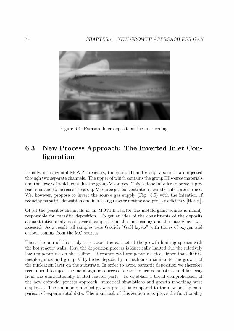
78 CHAPTER 6. NEW GROWTH APPROACH FOR GAN
Figure 6.4: Parasitic liner deposits at the liner ceiling
6.3 New Process Approach: The Inverted Inlet Con-
figuration
Usually, in horizontal MOVPE reactors, the group III and group V sources are injectedthrough two separate channels. The upper of which contains the group III source materialsand the lower of which contains the group V sources. This is done in order to prevent pre-reactions and to increase the group V source gas concentration near the substrate surface.We, however, propose to invert the source gas supply (Fig. 6.5) with the intention ofreducing parasitic deposition and increasing reactor uptime and process efficiency [Har04].
Of all the possible chemicals in an MOVPE reactor the metalorganic source is mainlyresponsible for parasitic deposition. To get an idea of the constituents of the depositsa quantitative analysis of several samples from the liner ceiling and the quartzbowl wasassessed. As a result, all samples were Ga-rich ”GaN layers” with traces of oxygen andcarbon coming from the MO sources.
Thus, the aim of this study is to avoid the contact of the growth limiting species withthe hot reactor walls. Here the deposition process is kinetically limited due the relativelylow temperatures on the ceiling. If reactor wall temperatures rise higher than 400C,metalorganics and group V hydrides deposit by a mechanism similar to the growth ofthe nucleation layer on the substrate. In order to avoid parasitic deposition we thereforerecommend to inject the metalorganic sources close to the heated substrate and far awayfrom the unintentionally heated reactor parts. To establish a broad comprehension ofthe new epitaxial process approach, numerical simulations and growth modelling wereemployed. The commonly applied growth process is compared to the new one by com-parison of experimental data. The main task of this section is to prove the functionality

6.3. NEW PROCESS APPROACH: THE INVERTED INLET CONFIGURATION 79
Figure 6.5: Sketch of inlet configuration and modelling of flow patterns: comparison forthe conventional (a) and the inverted inlet (b) geometry. The flow velocity is high on theammonia channel side because of a high mass flow and a comparably small cross sectionalarea where the mass flow passes through. Thus, for the conventional inlet the flow isdirected towards the ceiling by a vortex. The inverted case demonstrates no such effects.
of the growth approach.
6.3.1 Growth Modelling
The principal characteristics of the inverted and conventional inlet growth processes werestudied and compared using modelling. The modelling was performed by the Semicon-ductor Technology Research GmbH in Erlangen. The mathematical model is based onthe solution of the 2D/3D Navier-Stokes conservation equations describing flow, heattransfer, and multi-component diffusion of the gaseous mixture inside the reactor [Bir60],taking into account the specific reactor geometry, the inlet design and the presence ofwall deposits and particles. However, numerical simulation can only be performed forthe high temperature deposition regime. A brief introduction is found in chapter 3. Thekinetic mechanism of MOVPE gas-phase reactions is based on the work of Mihopoulos[Mih99]. To simulate the surface chemistry, a quasi-thermodynamic approach was usedas described in chapter 3. A further discussion of hydrodynamic effects is also found inchapter 3.
For high temperature GaN growth, the boundary conditions were defined by the experi-ments and they are summarized below (Table 6.1). For the established set of parametersin table 6.1 solely the inlet was switched from the conventional setting to the invertedone, thus facilitating the investigation of principal transport characteristics for the inletgeometries and their respective impacts on growth. In figure 6.6 the temperature distri-bution in the reactor and on the ceiling is presented. It is not influenced by the inlet

80 CHAPTER 6. NEW GROWTH APPROACH FOR GAN
Precursors flow rates TMGa = 6.63 ∗ 10−5mol/minNH3 = 5.80 ∗ 10−2mol/min
Carrier gas H2
Total flow 7.8 slmMO/ Hydride flow 6.8/ 1 slm
Growth temperature 1100CReactor pressure 200 mbar
Substrate: α-sapphire
Table 6.1: Boundary conditions for a standard GaN growth process
configuration.
central cross-section
ceiling
Figure 6.6: Temperature distribution in a cross sectional view and on the liner ceiling.
The inlet variation changes the transport, which governs the access of the reactive speciesto the sample surface. Thus, the flow patterns, as presented in Fig. 6.5, are compared forboth processes. In the ammonia channel the total flow is higher than on the MO channel.The upper channel has a larger cross-section than the lower channel in the vicinity ofthe separation plate edge, where the mixing of the two flows takes place. This leads toa much higher gas velocity at the separation plate end in the ammonia channel for theconventional inlet than for the inverted one. A turbulence at the tip of the separationplate results from this gas distribution. The total flow distribution 1 together with thedensity of the gas and the temperature gradient in the reactor leads to buoyancy drivenconvection (or natural convection) as is clearly seen by the vortex. As for the invertedinlet, the flow seems to distribute evenly into the heated susceptor area, forming a laminarflow. These flow phenomena, of course, have an immediate impact on the distribution of
1governed by forced convection and diffusion, as discussed in chapter 3.

6.3. NEW PROCESS APPROACH: THE INVERTED INLET CONFIGURATION 81
the species in the gasphase as we will discuss in the following.
TMGa
NH3conv.
conv. inv.
inv.
Figure 6.7: Comparison of NH3 and TMGa distribution for the conventional (a) and theinverted inlet (b) geometry. The concentrations are translated into colors: blue for lowand red for high concentrations. The ammonia and TMGa concentration close to theceiling is higher for the conventional inlet configuration.
Figure 6.7 serves as an illustration of growth species distribution in the central crosssection of the reactor for the conventional and inverted inlet case. The molar concentra-tions are translated into colors: red for high and blue for low concentrations. Ammoniaspreads towards the liner ceiling for the conventional case, whereas it is more homoge-nously distributed throughout the growth area for the inverted inlet. Qualitatively thesame behavior is predicted for the distribution of TMGa. Since it is injected close to theliner top it stays there. Its respective concentration is higher at the ceiling than for theinverted inlet, where the color scheme shows the highest concentration is to be found nearthe substrate.
Fig. 6.8 presents the transversal cross-section of the reactor at the location of the middle ofthe wafer and the distribution of monomethylgallium (MMGa), the main gallium reagentfor growth. For the conventional inlet growth process TMGa readily reaches the heatedregions of the reactor ceiling above the substrate providing favorable conditions for theformation of parasitic deposits. Therefore the concentration of MMGa is higher near theceiling of the reactor. In the inverted case the concentration of TMGa molecules is highercloser to the susceptor and react there to form the growth species MMGa.
Fig. 6.9 predicts the growth rate distribution in flow direction over the middle of thewafer according to modelling of non-rotated samples. The main reason for the changeof profiles is found in the distribution of the growth determining species near the heated

82 CHAPTER 6. NEW GROWTH APPROACH FOR GAN
MMGa
Conventional Inlet
Inverted Inlet
Figure 6.8: Modeling: Comparison of MMGa distribution for the conventional (a) and theinverted inlet (b) geometry. A transversal cross-section of the reactor is presented. Theconcentrations are translated into colors: blue for low and red for high concentrations.The MMGa concentration is lower towards the ceiling and higher towards the substratein the inverted inlet configuration
substrate. The susceptor region creates a strongly heated area on the reactor bottom. Thegrowth pattern is determined by the transport of growth limiting species to the susceptorsurface. The close injection of TMGa to the substrate for the inverted inlet leads toa shorter diffusion time for MMGa to reach the substrate. Therefore deposition startsdirectly at the rim of the heated susceptor, a deposition maximum is found. Afterward thegas phase is gradually depleted of the source chemicals in flow direction. The gas phaseis less strongly depleted of the nutrients toward the side walls of the reactor, becausethe gasphase at the sidewalls experiences the heated zone later, due to the disc shapeof the susceptor. Therefore the layers are thicker towards the edge of the wafer. Thegrowth maximum for the conventional inlet is positioned on the middle of the substrate.The MMGa has a longer diffusion length since it is delayed through a denser ammoniacontaining gas phase and forced convection carries the growth species further into thereactor.
All in all the effect of the conventional inlet on growth is an enhanced parasitic depositionby a factor of more than 3 on the quartz ceiling of the reactor as can be seen in Fig.6.10. The maximum of this deposition is unfortunately upstream of the wafer for theconventional process so that it can react catalytically with the process gases before theyreach the substrate whereas it is displaced downstream for the other geometry. Thereforeit is predicted that the inverted inlet process should be advantageous for high reactoruptimes and good morphology with respect to flaking and particle formation and a higherrun to run reproducibility.

6.3. NEW PROCESS APPROACH: THE INVERTED INLET CONFIGURATION 83
Figure 6.9: Expected growth profiles according to modelling in flow direction over themiddle of the wafer. For the conventional inlet (lower line) a growth maximum is expectedin the middle of the wafer. The inverted inlet (upper line) geometry exhibits a maximumat the front of the wafer.
6.3.2 Experimental Verification: Inverted to Conventional Inlet
Our experiments verify the predicted greatly reduced parasitic deposition in the invertedinlet geometry. Typically, at least 40 runs of 2µm thick GaN can be carried out withoutremoving parasitic deposits from the reactor ceiling instead of less than 10 growth runsfor the conventional growth process. Also the surface temperatures and the growth ratesremained constant from run to run with the new process. There are further characteristicswhich differ when comparing the transients (figure 6.11) for both growth processes:
• The growth rate of the nucleation layer is about one third higher for the invertedinlet geometry. This can be explained taking into account the different MMGaconcentrations near the substrate surface. In the conventional inlet, the MMGaconcentration is higher near the ceiling of the reactor and just a limited amountwill diffuse through the boundary layer contributing to the GaN on the substrate.In contrast, in the inverted inlet, where the TMGa is supplied through the lowerchannel, the MMGa concentration in the vicinity of the substrate is higher, it willreact more efficiently with the N-containing species, resulting in an increase of thenucleation growth rate [Kal04].
• The coalescence time is significantly shorter for the inverted inlet geometry. Areason for the shorter coalescence might be the higher availability of MMGa nearthe substrate therefore enhancing lateral growth, in turn leading to faster coalescence(compare chapter 7).
• The growth rate in the HT regime is lower for the inverted inlet geometry. As for the

84 CHAPTER 6. NEW GROWTH APPROACH FOR GAN
7.3
6.7
6.1
5.5
4.9
4.3
3.7
3.1
2.5
1.9
1.3
0.7
0.1
2.0
1.9
1.7
1.5
1.4
1.2
1.0
0.9
0.7
0.5
0.4
0.2
0.0
Conventional Inlet
Inverted Inlet
Figure 6.10: Comparison of growth rate distribution over the ceiling of the horizontalreactor above the substrate (marked with a circle) for the conventional (upper image)and the inverted inlet (lower image) geometry. The growth rates are translated intocolors: blue for low and red for high rates. The growth rate is more than three times ashigh for the conventional inlet compared to the inverted inlet. The deposition maximumis positioned upstream of the substrate for the conventional inlet.
lower growth rate in the HT regime some mechanism of material losses seems to beactivated at the reversed precursor supply associated with the total species flow andgas residence times. It might as well be due to the fact that the measuring pointfor growth rate determination is located in the middle of the wafer, whereas themaximum deposition rate is at the wafer rim. Therefore the growth rate depends,in short, on the configured growth parameters, which need to be optimized.
Fig. 6.12 presents thickness mappings of both runs. Considering the thickness distributionit becomes apparent that the growth profiles differ considerably. For the conventionalgrowth process the growth profile is convex whereas it is concave for the inverted inletgeometry.
Starting from figure 6.9 and using wafer rotation, concave growth profiles are produced inthe inverted inlet. The standard deviation in thickness with 2mm edge exclusion is 6.5%and 10.4% for the conventional and the inverted inlet geometry, respectively. Due to thedifferent convective to diffusive reactive species’ flow ratios, each inlet geometry will needits own strategy to obtain optimum uniformity (compare chapter 7).

6.3. NEW PROCESS APPROACH: THE INVERTED INLET CONFIGURATION 85
nucl.:
0.35 µm/h
t = 64 min
HT: 1.46 µm/h
t = 50 min
nucl.:
0.46 µm/hHT: 1.25 µm/h
Figure 6.11: Comparison of transients (reflection measurement taken from the wafer mid-dle) for both growth processes. The coalescence time is significantly shorter and thegrowth rate in the HT regime lower for the inverted inlet geometry.
Figure 6.12: GaN growth profiles obtained using the conventional inlet (a) and the in-verted inlet (b) geometry. For the conventional inlet a convex growth profile is observed,for the inverted inlet a concave profile is found.
The surface roughness is comparable at the microscopic and nanometer scale for bothprocesses as figure 6.13 demonstrates. The AFM inset shows a slightly different surfacemorphology for the inverted inlet. Considering that the coalescence phase, which cancontribute to the surface morphology, is somewhat shorter and the overall thickness isthinner for the ”inverted” growth run, the change in morphology may be explainable.
The structural quality of the material is state of the art and very similar for both samplestaking the different total layer thicknesses into account. The GaN layer grown by theconventional process the full-width at half maximum (FWHM) of the 002 rocking curveis 233 for the inverted inlet GaN film the FWHM is 244 arcsec.
The electrical properties of the grown material were investigated by room temperatureHall measurements and Lehighton contactless sheet resistance mappings. It was foundthat the sheet resistance is lower by 10% for the inverted inlet at an absolute valueof around 360Ω
¤ and its uniformity over the wafer is quite comparable for both process

86 CHAPTER 6. NEW GROWTH APPROACH FOR GAN
conventional inverted
500 µm 500 µm
conventionalconventional invertedinverted
rms = 0.62 nm rms = 0. 66 nm
Figure 6.13: Comparison of surface morphology at microscopic (upper image) andnanometer scale (lower image)for both processes. The AFM inset shows a slightly roughersurface for the inverted inlet.
approaches. Intentionally Si doped samples exhibited a carrier concentration of 1.0 and1.2 × 1017cm3 and an electron mobility of 605 and 544cm2/V s for the conventional andthe inverted geometry, respectively. Here again the samples are state of the art andcomparable for both growth processes. Table 6.2 summarizes the characteristics of bothprocesses. However, it is important to further characterize the layer properties, so farthese results prove the functionality of the new process.
Parameter Conventional inlet Inverted inletGrowth rate at 550C (µm/h) 0.35 0.46Growth rate at 1100C (µm/h) 1.46 1.25
Coalescence time (min) 64 50Growth profile Convex ConcaveThickness (µm) 3.90± 0.25µm (6.5%) 3.32± 0.35µm (10.4%)
Roughness, rms (nm) 0.622 0.655XRD: FWHM (0002) (arcsec) 233 244
Sheet resistance (Ω¤) 402± 129 (32%) 362± 101 (28%)
n300 (*1017 cm–3) 1.0 1.2µHall300K (cm2/V s) 605 544
Table 6.2: Comparison of morphological, structural, electrical and uniformity data for theconventional and inverted inlet geometries

6.3. NEW PROCESS APPROACH: THE INVERTED INLET CONFIGURATION 87
6.3.3 Conclusion
Improving reproducibility was the aim of this chapter. A new growth approach for hori-zontal reactors is therefore introduced, in which the metalorganic source is injected nearthe substrate unlike the conventional process, resulting in reduced parasitic deposition.Experiment and modelling verify the suitability of the new growth approach for enhancedreproducibility. Moreover the new approach leads to a fourfold reactor uptime withoutchanging reactor quartz parts. The structural, morphological and electrical characteris-tics of the grown layers are comparable for both processes. The main difference in thegrowth processes are the growth profiles which indicate that growth optimization mustbe carried out differently for both processes.

88 CHAPTER 6. NEW GROWTH APPROACH FOR GAN

Chapter 7
Optimizing GaN Growth
Now that the functionality of the new GaN growth approach is proven the optimizationof layers with respect to HEMT application can be tackled. In this context the majoringredients for an ideal GaN template should be reviewed:
1. ”Manufacturing uniformity” in terms of homogeneous layer characteristics and re-producible layer growth with a high yield.
2. Good structural quality with low dislocation densities for high amplification by highchannel conductivity at high frequencies;
3. A smooth surface with a low defect density, important for the growth of sharpinterfaces as well as for device processing;
This chapter deals with the fulfillment of these criteria. First of all the homogeneityin terms of thickness distribution is addressed and then the improvement of electrical,structural and morphological properties is faced.
7.1 Homogeneity Optimization
The new process prevents parasitic GaN growth on the hot reactor walls by invertingthe source gas supply and therefore leads to enhanced reproducibility and higher reactoruptimes. As reported in chapter 6 electrical and structural layer characteristics are quitecomparable for both inlet geometries. However, the inversion of the precursor supplyhas a drawback consisting in a fairly high growth rate non-uniformity, with a typicalstandard deviation in thickness of around 10%. However, HEMT devices for power appli-cations consume large areas of typically several mm2. Thickness uniformity is therefore
89

90 CHAPTER 7. OPTIMIZING GAN GROWTH
paramount. Due to different flow dynamics and species distribution in comparison to theconventional process, the inverted growth process also needs different strategies to obtainuniform layers.
Flow-mechanical aspects in our reactor system are investigated in order to achieve ahomogeneous thickness distribution. Due to the strong temperature dependence of thenucleation layer as well as the HT-GaN, temperature uniformity over the wafer is a pre-requisite [Shi04]. Besides this, the most important factor is the distribution of the growthrate determining species in the gas phase close to the substrate. This distribution is alsotemperature dependent (”cold finger” effect) and moreover relies on parameters such asthe carrier gas nature and flow velocities [Dau01, Har01]. For homogeneity optimizationwe particularly focus on the role of different carrier gases - nitrogen and hydrogen - duringIII-nitride growth.
upper channel
lowerchannel
upper channel
lowerchannel substrateTMGa + carrier
NH3+ carrier
forced convection
diffusion
Figure 7.1: Forced convection and Fickian diffusion dominate the distribution of growthlimiting species in the reactor and thus the homogeneity over the wafer. Forced convectionmoves the species in flow direction and parallel to the substrate surface, while diffusionmoves the species perpendicular to the flow direction and to the substrate surface.
7.1.1 Optimization Strategy
Apparently, a flow parameter optimization becomes necessary to enhance the uniformity.Starting point for our considerations is the expected growth profiles according to modellingin flow direction over the middle of the wafer. The inverted inlet geometry exhibits amaximum at the front of the wafer with a nonlinear decrease over the wafer as seenin figure 6.9 in chapter 6. In order to linearize the growth rate and thus enhance thethickness uniformity the deposition maximum needs to be shifted closer to the substrate.A beneficial side effect is the enhanced growth efficiency.
According to chapter 3 the distribution of chemical species in the mass transport limitedgrowth regime is determined by the hydrodynamics of the given flow. As depicted infigure 7.1 the mass transport is governed by forced convective (imposed pressure gradient)

7.1. HOMOGENEITY OPTIMIZATION 91
and diffusive (Fickian diffusion) flux1 of the growth limiting chemical species within thereactor, thus, determining the thickness homogeneity over the wafer [Str99]. A peculiarityarises when nitrogen is used as the carrier gas: In a high temperature process, as it isthe case for GaN deposition, the presence of a region of colder gas (so called cold finger)is observed, penetrating from the inlet into the deposition zone (compare chapter 3). Ifthe flow rate is low and the thermal conductivity is high, heat is conducted sufficientlyfast relative to convection, so that there are no large temperature gradients around thesusceptor. However, if the gas velocity is fast and/or a gas with lower thermal conductivity(e.g. N2) is used a thermal boundary layer develops. This can influence the decompositionof growth species and therefore change the supply of species to the surface.
In our reactor setup forced convection is driven by the pressure gradient between gas in-and outlet and the gas flow in the liner, thus dominating the flow velocity vg, which isdefined as
vg =Qtot · patm
A · ptot
(7.1)
The flow velocity is controlled by the total flow rate Qtot and the reactor pressure ptot.Here, patm is the atmospheric ambient pressure (= 1bar) and A stands for the cross-sectional area of either the inlet channel or the whole liner, depending on the gas velocitywhich is to be determined. Increasing the total flow leads to a different flow profile andhence to a different growth species distribution in the reactor.
Mass transport to the substrate itself is basically driven by Fickian diffusion and propor-tional to the mass flow m, which is defined as
m = ΣQiρi
Ai
(7.2)
where Qi is the total flow in channel i (either group III or V inlet) and ρi its respectivedensity in the cross section Ai. Thus changing the density of the gas in a channel willyield a change of diffusion of the species towards the substrate.
Following the aforementioned dependencies two approaches are chosen.
1. The flow velocity is enhanced by increasing the total flow of H2 carrier gas in thereactor. Thus the gas phase depletion of growth species is reduced, due to shorterresidence times.
2. Enhancing flow velocity and changing the diffusion rate by increasing the totalflow in N2 ambient, thus increasing both viscosity and density of the carrier gas.
1and natural convective flux (due to thermal gradients) which is, however, rather negligible.

92 CHAPTER 7. OPTIMIZING GAN GROWTH
Concurrently, the thermal conductivity within the gasphase is reduced, thus MMGa2
decomposition delayed.
Process modelling is employed to clarify the flow dynamics in this inlet configuration.
7.1.2 Experimental Results
In order to exclude effects due to different nucleation parameters, nucleation was alwayscarried out with H2 carrier gas at 550C until a layer thickness of about 25nm was reached.After layer annealing HT growth was performed at constant conditions of 200mbar reactorpressure and 1100C. For the uniformity investigation the total amount of hydrogen ornitrogen carrier gas on the MO channel was stepwise increased right before HT growth,according to figure 7.2. The alkyl inlet was chosen since the growth limiting species is theMO precursor. The main growth parameters for our GaN growth process are summarizedin table 7.1
GaN nucleation layer Annealing GaN epilayergrowth growth (HT growth)
Temperature 550C 1000C 1100CTMGa 15 sccm - 25 sccmNH3 2.2 slm 2 slm 3.3 slmV/III ratio 1482 - 1334Total flow 8 slm 8 slm 9...15 slmFlow MO side 1 slm 1 slm 1...7 slmFlow Hyd side 7 slm 7 slm 8 slmReactor pressure 200 mbar 200 mbar 200 mbarTime 1.5 min 3 min -Thickness 25 nm - ∼ 2 µm
Table 7.1: Growth parameters for a standard GaN growth process in an AIX 200/4 RF-Sreactor (TMGa bubbler was used at a pressure of 1000 mbar and a temperature of 0C)
The wafers are characterized ex situ using the film thickness measurement method intro-duced in chapter 4. The standard deviation of the thickness distribution, as determined byfilm thickness measurements, is a measure of the achieved thickness uniformity. Growthrates are calculated with the in-situ recorded reflectance transient at 600 nm.
Figure 7.3 presents growth rate (right) and thickness uniformity (left) versus the amountof additional carrier gas introduced through the lower inlet. Adding hydrogen, the growth
2MMGa is considered as the growth limiting species.
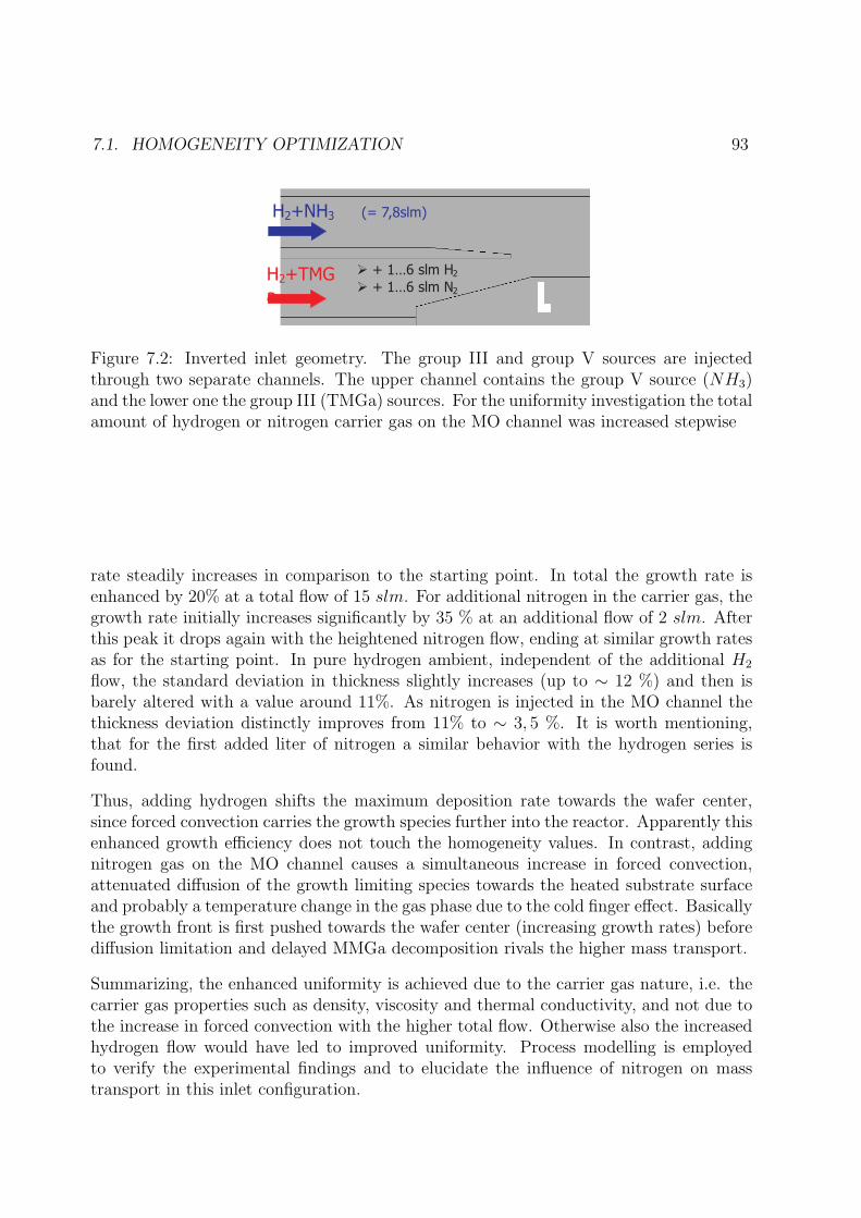
7.1. HOMOGENEITY OPTIMIZATION 93
H2+TMG
a
H2+NH3 (= 7,8slm)
Ø + 1…6 slm H2
Ø + 1…6 slm N2
Figure 7.2: Inverted inlet geometry. The group III and group V sources are injectedthrough two separate channels. The upper channel contains the group V source (NH3)and the lower one the group III (TMGa) sources. For the uniformity investigation the totalamount of hydrogen or nitrogen carrier gas on the MO channel was increased stepwise
rate steadily increases in comparison to the starting point. In total the growth rate isenhanced by 20% at a total flow of 15 slm. For additional nitrogen in the carrier gas, thegrowth rate initially increases significantly by 35 % at an additional flow of 2 slm. Afterthis peak it drops again with the heightened nitrogen flow, ending at similar growth ratesas for the starting point. In pure hydrogen ambient, independent of the additional H2
flow, the standard deviation in thickness slightly increases (up to ∼ 12 %) and then isbarely altered with a value around 11%. As nitrogen is injected in the MO channel thethickness deviation distinctly improves from 11% to ∼ 3, 5 %. It is worth mentioning,that for the first added liter of nitrogen a similar behavior with the hydrogen series isfound.
Thus, adding hydrogen shifts the maximum deposition rate towards the wafer center,since forced convection carries the growth species further into the reactor. Apparently thisenhanced growth efficiency does not touch the homogeneity values. In contrast, addingnitrogen gas on the MO channel causes a simultaneous increase in forced convection,attenuated diffusion of the growth limiting species towards the heated substrate surfaceand probably a temperature change in the gas phase due to the cold finger effect. Basicallythe growth front is first pushed towards the wafer center (increasing growth rates) beforediffusion limitation and delayed MMGa decomposition rivals the higher mass transport.
Summarizing, the enhanced uniformity is achieved due to the carrier gas nature, i.e. thecarrier gas properties such as density, viscosity and thermal conductivity, and not due tothe increase in forced convection with the higher total flow. Otherwise also the increasedhydrogen flow would have led to improved uniformity. Process modelling is employedto verify the experimental findings and to elucidate the influence of nitrogen on masstransport in this inlet configuration.
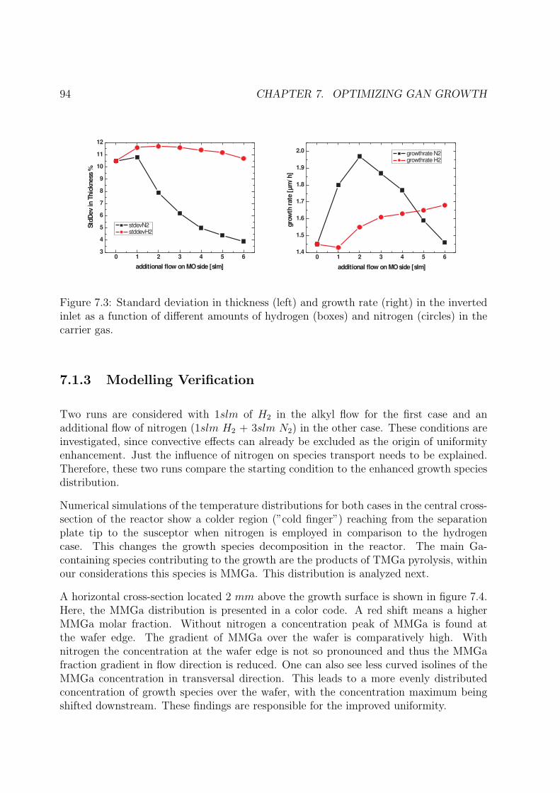
94 CHAPTER 7. OPTIMIZING GAN GROWTH
0 1 2 3 4 5 63
4
5
6
7
8
9
10
11
12
Std
Dev
inThic
kness
%
additional flow on MOside [slm]
stdevN2stddevH2
0 1 2 3 4 5 61.4
1.5
1.6
1.7
1.8
1.9
2.0
additional flow on MOside [slm]
gro
wth
rate
[µm
/h]
growthrate N2growthrate H2
Figure 7.3: Standard deviation in thickness (left) and growth rate (right) in the invertedinlet as a function of different amounts of hydrogen (boxes) and nitrogen (circles) in thecarrier gas.
7.1.3 Modelling Verification
Two runs are considered with 1slm of H2 in the alkyl flow for the first case and anadditional flow of nitrogen (1slm H2 + 3slm N2) in the other case. These conditions areinvestigated, since convective effects can already be excluded as the origin of uniformityenhancement. Just the influence of nitrogen on species transport needs to be explained.Therefore, these two runs compare the starting condition to the enhanced growth speciesdistribution.
Numerical simulations of the temperature distributions for both cases in the central cross-section of the reactor show a colder region (”cold finger”) reaching from the separationplate tip to the susceptor when nitrogen is employed in comparison to the hydrogencase. This changes the growth species decomposition in the reactor. The main Ga-containing species contributing to the growth are the products of TMGa pyrolysis, withinour considerations this species is MMGa. This distribution is analyzed next.
A horizontal cross-section located 2 mm above the growth surface is shown in figure 7.4.Here, the MMGa distribution is presented in a color code. A red shift means a higherMMGa molar fraction. Without nitrogen a concentration peak of MMGa is found atthe wafer edge. The gradient of MMGa over the wafer is comparatively high. Withnitrogen the concentration at the wafer edge is not so pronounced and thus the MMGafraction gradient in flow direction is reduced. One can also see less curved isolines of theMMGa concentration in transversal direction. This leads to a more evenly distributedconcentration of growth species over the wafer, with the concentration maximum beingshifted downstream. These findings are responsible for the improved uniformity.
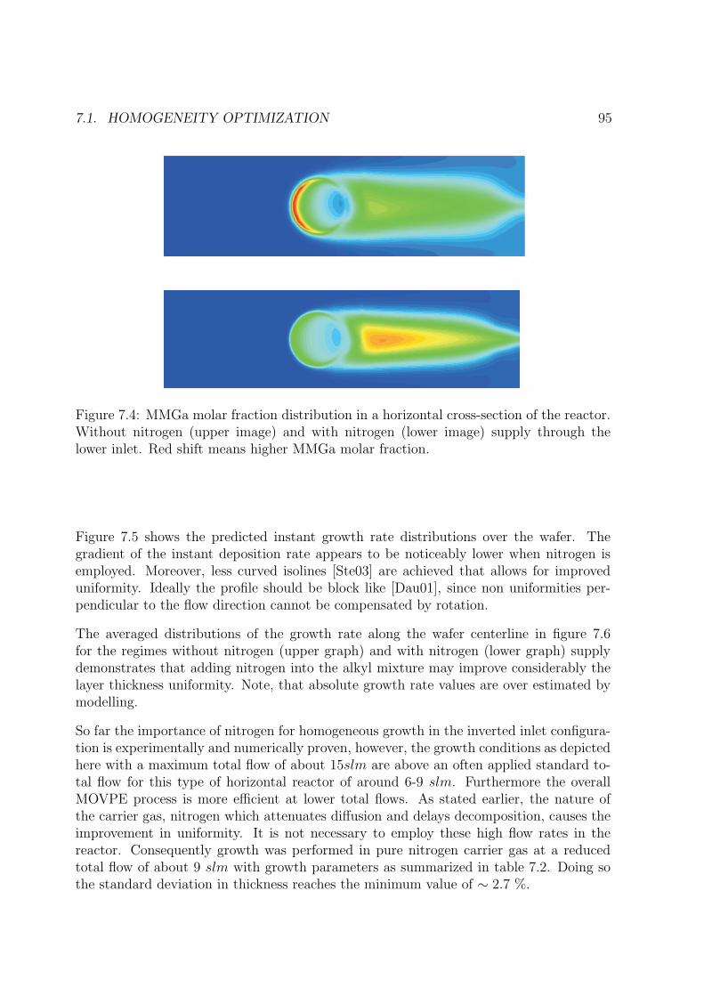
7.1. HOMOGENEITY OPTIMIZATION 95
Figure 7.4: MMGa molar fraction distribution in a horizontal cross-section of the reactor.Without nitrogen (upper image) and with nitrogen (lower image) supply through thelower inlet. Red shift means higher MMGa molar fraction.
Figure 7.5 shows the predicted instant growth rate distributions over the wafer. Thegradient of the instant deposition rate appears to be noticeably lower when nitrogen isemployed. Moreover, less curved isolines [Ste03] are achieved that allows for improveduniformity. Ideally the profile should be block like [Dau01], since non uniformities per-pendicular to the flow direction cannot be compensated by rotation.
The averaged distributions of the growth rate along the wafer centerline in figure 7.6for the regimes without nitrogen (upper graph) and with nitrogen (lower graph) supplydemonstrates that adding nitrogen into the alkyl mixture may improve considerably thelayer thickness uniformity. Note, that absolute growth rate values are over estimated bymodelling.
So far the importance of nitrogen for homogeneous growth in the inverted inlet configura-tion is experimentally and numerically proven, however, the growth conditions as depictedhere with a maximum total flow of about 15slm are above an often applied standard to-tal flow for this type of horizontal reactor of around 6-9 slm. Furthermore the overallMOVPE process is more efficient at lower total flows. As stated earlier, the nature ofthe carrier gas, nitrogen which attenuates diffusion and delays decomposition, causes theimprovement in uniformity. It is not necessary to employ these high flow rates in thereactor. Consequently growth was performed in pure nitrogen carrier gas at a reducedtotal flow of about 9 slm with growth parameters as summarized in table 7.2. Doing sothe standard deviation in thickness reaches the minimum value of ∼ 2.7 %.

96 CHAPTER 7. OPTIMIZING GAN GROWTH
Figure 7.5: Instant growth rate mappings for the regimes without nitrogen (left) and withnitrogen (right) supply through the lower inlet. Less curved isolines are achieved withnitrogen.
radial position, m
gro
wth
rate
,µm
/h
-0.02 -0.01 0 0.01 0.022
2.25
2.5
2.75
3
3.25
3.5
3.75
4
4.25
without nitrogen
with nitrogen
Figure 7.6: Growth rate distribution for rotated wafers along the wafer centerline for theregimes without nitrogen (upper line) and with nitrogen (lower line) supply through thelower inlet. Absolute growth rate values are over estimated by modelling.
7.1.4 Conclusion
It has been found that inversion of the precursor supply has a drawback when consideringthe thickness uniformity. Two approaches were looked at to change the growth speciesdistribution: An increase in forced convection and/or change of diffusive transport anddelayed growth species decomposition. Uniformity can only be improved by changing thenature of the carrier gas, thus, modifying the diffusive transport and decomposition ofgrowth species by adding nitrogen into the alkyl mixture. Thus, the growth species aredistributed more uniformly above the susceptor. This way, in N2 atmosphere a standarddeviation in thickness of less than 3% is achieved in comparison to 10% for H2 ambi-ent. The investigation of layer properties is necessary to understand the influence of thenitrogen carrier gas on GaN epilayers characteristics.

7.2. ON THE EFFECT OF N2 ON GAN GROWTH 97
7.2 On the Effect of N2 on GaN Growth
For the MOVPE of GaN the majority of epitaxy groups report the usage of hydrogenas the preferred carrier gas. Successful growth processes in hydrogen have long beenestablished. Nevertheless, there are others as well. Amano et al. used nitrogen as theambient gas [Ama84]. Nakamura et al. reported the use of a gas mixture of H2 andN2 as the sub-flow gas [Nak91a]. These GaN epilayers, grown in the presence of N2,show good uniformity and high quality. However, the majority of growth experimentsin nitrogen led to the opinion that pure N2 is not only detrimental to the morphologyand the structural quality of GaN but also to the electrical properties [Wan01]. Thereason for these controversial findings [Muk98, Nak99, Jav02] may be due to differentMOVPE reactor setups and non-adapted processes to the nitrogen ambient (one-to-onecopy of hydrogen process). There is no detailed study of the influence of nitrogen on GaNgrowth. Thus, in this section GaN growth in different atmospheres, from pure hydrogento pure nitrogen, will be systematically investigated.
7.2.1 Experimental Results
GaN epilayergrowth (HT growth)
Temperature 1100CTMGa 25 sccmNH3 2.2 slmV/III ratio 877Carrier gas 0...100% N2
Total flow 9 slmFlow MO side 6.5 slmFlow Hyd side 2.5 slmReactor pressure 200 mbarThickness > 2 µm
Table 7.2: Growth parameters for the GaN growth process with increasing nitrogenamount in the gas phase
For all samples nucleation layer growth and annealing were carried out using H2 carrier gasunder identical conditions as stated in table 7.1 in section 7.1. After the annealing process,growth was resumed and the successive high temperature growth step (HT-growth) wasperformed with different ratios of H2/N2 carrier gas mixtures, ranging from 0% (purehydrogen atmosphere) to 100% nitrogen at 1100C while the total flow was kept constantat 9slm. In this way, the carrier gas composition was changed right after the annealing

98 CHAPTER 7. OPTIMIZING GAN GROWTH
step. The main growth parameters for the HT growth process are summarized in table7.2
500µm500µm500µm500µm
10 % N2
40 % N2
75 % N2
100 % N2
Figure 7.7: Nomarski-microscopy of samples grown with increasing amount of nitrogenin the ambient. In case of pure nitrogen the surface drastically worsens. Hexagonalstructures and even small ”turrets” can be observed.
Pure H2
RMS = 0.388 nm
Pure N2
RMS = 0.368 nm
Figure 7.8: AFM micrographs of GaN layers grown under pure H2 (left) or N2 (right).
Figure 7.7 reveals the surface morphology as seen via Nomarski-microscopy of samplesgrown with increasing amount of nitrogen in the ambient. The morphology on the mi-crometer scale is rather smooth for any sample grown under hydrogen or mixtures ofhydrogen and nitrogen. In case of pure nitrogen the surface drastically worsens. Hexag-onal structures and even small ”turrets” can be observed. Any further processing stepstowards HEMT devices, such as metallization steps etc., are out of question for such asample. Morphology optimization becomes necessary. However, all samples are specularwhen examined by the eye.

7.2. ON THE EFFECT OF N2 ON GAN GROWTH 99
On the nanometer scale, the surface morphology also changes from H2 to N2 (Figure 7.8).For pure H2, the surface exhibits smooth and parallel atomic steps. The higher the N2
content the more the steps become round and pits are observed. This is a first indicationof an increased dislocation density. Its emphasized, however, that the roughness differsslightly but is comparably low (RMS: ∼ 0.3nm) for both samples.
The often reported surface degradation develops probably due to the different diffusionlength of the adatoms on the surface. Due to the increased gas density in nitrogen,the adatoms have smaller mean free paths and cannot migrate over long distances to findfavorable adsorption sites [Hal01, Wan01]. The structural properties may also be affected:
0 20 40 60 80 100
300
400
500
600
700
800
900
N2 content in gasphase(%)
FW
HM
(arc
sec.)
GaN (002)
GaN (102)
Figure 7.9: The rocking curves of the (002) demonstrate similar FWHM values of about330arcsec, while the (102) peaks increases significantly.
The crystal properties of the GaN epilayers were probed by X-ray diffraction using thesymmetric (002) and asymmetric (102) reflection: The rocking curves of the (002) demon-strate similar FWHM values of about 330arcsec, with only slight variations as the nitrogencontent in the gas phase is changed, as seen in figure 7.9. In contrast, the FWHM of the(102) peaks increases significantly from 400 to 900arcsec. The (102) rocking curve isbroadened by all types of threading dislocations (TDs) such as the edge, screw and mixedtypes of TDs, while the (002) rocking curve is only broadened by pure screw and mixedtypes of TDs [Wan01, Bot01]. Obviously, mainly the edge dislocation density increaseswith increasing N2 content.
Grain boundaries are causal for dislocation formation. Apparently, in comparison to a

100 CHAPTER 7. OPTIMIZING GAN GROWTH
pure hydrogen atmosphere, smaller grains coalesce and dislocations arise at the edges ofthe islands. Higher dislocation densities, in turn, might be associated with strain relax-ation, since dislocations accommodate the grown film to the substrate. Strain relaxationcan be proven by, for example, PL measurements.
3.45 3.46 3.47 3.48 3.49 3.50 3.51 3.52
H2:
DBX: 3.484 eVFWHM: 2.3 meV
100% H2100% N2
Intensity
Energy [eV]
N2:
DBX: 3.480 eVFWHM: 2.5 meV
Figure 7.10: The donor bound exciton (DBX) peak is shifted towards lesser energies foran epitaxial growth run in pure nitrogen ambient in comparison to a growth run in pureH2.
Photoluminescence measurements (figure 7.10) reveal a donor bound exciton (DBX) peakshifted towards lesser energies for an epitaxial growth run in pure nitrogen ambient incomparison to a pure H2 ambient. GaN layers grown on sapphire suffer from compressivestrain. The GaN band gap increases in case of biaxial in-plane compression compared tofully relaxed GaN. The DBX energy therefore increases with increasing compressive strainin the layers. A lesser compressive strain is thus found in the layer [Cho06]. Similar resultswere obtained by Raman spectroscopy. The amount of strain decreases with increasingN2 content. These results indicate that internal compressive strain is released possiblyby dislocation formation. Other groups also reported [Li04] different stress states whenusing nitrogen as the carrier gas, however did not mention the potential cause.
The degradation of the structural quality should also lead to a measurable impact on theelectrical data, which is investigated next.
The electrical properties of the grown material were investigated by room temperatureHall measurements. Intentionally Si-doped samples exhibited a distinct impact of the

7.2. ON THE EFFECT OF N2 ON GAN GROWTH 101
0 20 40 60 80 1000
100
200
300
400
500
600
µHall
ns
N2 content in gasphase [%]
Hall
mobilit
y[c
m2
]
5.00E+016
1.00E+017
1.50E+017
2.00E+017Carrie
rconcentra
tion
[cm
-3]
Figure 7.11: Hall measurements at room temperature.
carrier gas on the mobility of the GaN film. As the nitrogen content increases the mobilitydrops strongly from 488 to below 100cm2/V s at constant carrier concentration around1× 1017cm−3. Obviously the deterioration of the electrical characteristics is related to areduction of crystal structure quality with increasing nitrogen content. In particular thegenerated edge dislocations are electrically active,acting as acceptor like traps (comparechapter 8), and as scatter centers and thus carrier mobility is reduced (Eastman et al[Ng98]).
A lot of evidence has already been presented that the layer morphology, the structuralquality and the electrical properties degrade and more dislocations are induced with in-creasing nitrogen content. The origin of these effects must be correlated with growthand thus with the morphology development. Hence, the growth transients will clarify theunderlying growth mechanism.
The in situ measured reflectance transients at a wavelength of 600 nm for several growthruns with different carrier gas mixtures are presented in figure 7.12. The low temperaturegrowth step, as well as the annealing step, use hydrogen as carrier gas. After these growthsteps the coalescence phase starts in which the nuclei grow together. The beginning ofthis phase is denoted by the first dotted line in the transients. Gradually oscillations formwhich reach a constant intensity after complete two dimensional growth is observed. Ineach of the transients the second dotted line denotes the onset of complete 2D growth.With increasing nitrogen content in the gas phase (from bottom to top) the coalescencetime (and therefore the “coalescence thickness”) decreases drastically from 2200 to 100seconds. The coalescence time and thickness correlates with the size of the nuclei before
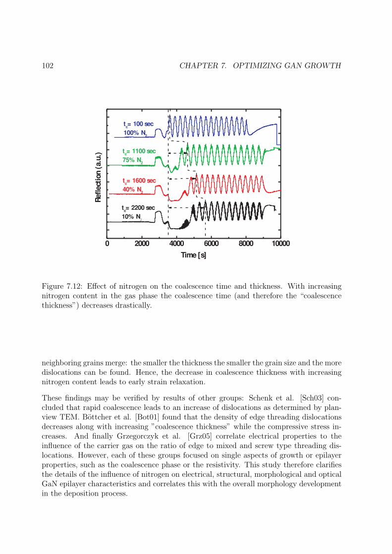
102 CHAPTER 7. OPTIMIZING GAN GROWTH
0 2000 4000 6000 8000 10000
tc= 2200 sec
10% N2
tc= 1600 sec
40% N2
tc= 1100 sec
75% N2
Refl
ecti
on
(a.u
.)
tc= 100 sec
100% N2
Time [s]
Figure 7.12: Effect of nitrogen on the coalescence time and thickness. With increasingnitrogen content in the gas phase the coalescence time (and therefore the “coalescencethickness”) decreases drastically.
neighboring grains merge: the smaller the thickness the smaller the grain size and the moredislocations can be found. Hence, the decrease in coalescence thickness with increasingnitrogen content leads to early strain relaxation.
These findings may be verified by results of other groups: Schenk et al. [Sch03] con-cluded that rapid coalescence leads to an increase of dislocations as determined by plan-view TEM. Bottcher et al. [Bot01] found that the density of edge threading dislocationsdecreases along with increasing ”coalescence thickness” while the compressive stress in-creases. And finally Grzegorczyk et al. [Grz05] correlate electrical properties to theinfluence of the carrier gas on the ratio of edge to mixed and screw type threading dis-locations. However, each of these groups focused on single aspects of growth or epilayerproperties, such as the coalescence phase or the resistivity. This study therefore clarifiesthe details of the influence of nitrogen on electrical, structural, morphological and opticalGaN epilayer characteristics and correlates this with the overall morphology developmentin the deposition process.

7.3. ELECTRICAL AND STRUCTURAL OPTIMIZATION WITH NITROGEN 103
7.2.2 Conclusion
Nitrogen is crucial for improved thickness homogeneity, but apparently nitrogen not onlychanges the surface morphology but it affects the growth mode in the early stages ofdeposition. From the presented data it is found that untimely recovery of the reflectancesignal, i.e. start of 2D growth, leads to GaN layers which contain a larger number ofedge type dislocations. Dislocations, in turn, influence the strain in the layer, leading tomore relaxed GaN layers when grown in nitrogen ambient. Dislocation scattering is thevery probable source of the decline in electrical data. As a result a larger ”coalescencethickness” is preferred, since it reduces the density of dislocations. Therefore a strategyneeds to be developed with which coalescence can be controlled despite the nitrogenambient needed for uniform layers.
7.3 Electrical and Structural Optimization with Ni-
trogen
For high power and high speed performance of HEMTs it is of primal importance tomaximize the channel sheet carrier concentration without reducing electron mobility andsaturation velocity, thus, to form a highly conductive GaN channel. Therefore -in addi-tion to a highly uniform GaN template- the optimization of morphology, structural andelectrical quality is required, allowing for control of dislocation types and densities.
In this section the strategy is developed with which highly uniform and state of theart material quality GaN films are grown, despite the effects of nitrogen on morphologydevelopment.
7.3.1 Aim to Prolong Coalescence in N2
An often reported approach towards prolonged coalescence is either lowering the depo-sition temperature and/or the V/III ratio [Fig00, Yan00, Kal03] during the coalescencephase. Originating from growth in pure N2 ambient, as shown in the foregoing discussion,we applied both methods as summarized in table 7.3. Nucleation layer growth and an-nealing conditions take place in hydrogen ambient and are the same as stated in table 7.2.During the coalescence phase the temperature was reduced to 1000 C and afterwardsincreased to epilayer growth temperature of 1100 C. In the next growth run the V/IIIratio was distinctly reduced to 485 in comparison to 877 during the HT-GaN epilayergrowth.
The resulting reflectance transients are presented in figure 7.13. In either case an im-mediate onset of small Fabry-Perot oscillations is observed. This suggests that, contrary

104 CHAPTER 7. OPTIMIZING GAN GROWTH
Coalescence HT-GaNlower T lower V/III
Temperature 1000 C 1000C 1100 CTMGa 25 sccm 25 sccm 25 sccmNH3 2.2 slm 1.2 slm 2.2 slmV/III ratio 877 485 877Carrier gas N2 N2 N2
Total flow 9 slm 9 slm 9 slmThickness > 2 µm
Table 7.3: Growth parameters for the prolonged coalescence run in nitrogen ambient.
0 2000 4000 6000 8000 10000 12000
Reflection
[arb
.units]
Time [s]
732
0 2000 4000 6000 8000 10000 12000
Rele
ctt
ion
[arb
.units]
Time [s]
736
Tc=1000°C
T =1100°C
V/III = 485
V/III = 867
0 2000 4000 6000 8000 10000 12000
Reflection
[arb
.units]
Time [s]
732
0 2000 4000 6000 8000 10000 12000
Rele
ctt
ion
[arb
.units]
Time [s]
736
Tc=1000°C
T =1100°C
V/III = 485
V/III = 867
Figure 7.13: Reflectance transients of two growth runs in pure nitrogen ambient. Pro-longed coalescence in neither achieved by applying a lower coalescence temperature Tc
nor lower V/III ratio.
to our intention, 2D growth begins. On a morphological scale the coalescence mode isnot controllable in nitrogen carrier gas. The electrical characterization by Hall measure-ments at room temperature of the intentionally Si-doped GaN yields very low electronmobilities. Applying a lower coalescence temperature results in an electron mobility of69 cm2/V s at carrier concentrations of 1 ×1017 cm−3. Using a lower V/III ratio duringcoalescence results in a mobility of 110 cm2/V s at a carrier concentration of 5.5 ×10¹⁷
cm−3. In either growth run the surface of the samples reveal similar features to the purenitrogen sample from figure 7.7: Hexagonal forms and turrets are observed.
A lengthened coalescence under nitrogen influence becomes impossible in our inlet con-figuration. Lacking control of coalescence results in poor electrical data. So the questionarises whether it is an inherent property of nitrogen (thus a matter of growth chemistry)or due to accelerated coalescence that the crystalline quality of GaN layers degrades.

7.3. ELECTRICAL AND STRUCTURAL OPTIMIZATION WITH NITROGEN 105
7.3.2 Role of Nitrogen in 2D Growth
To clarify this matter GaN was grown on a ”hydrogen template”, meaning the carriergas composition was stepwise changed towards pure nitrogen, after the GaN film fullycoalesced in H2 ambient. Consequently the coalescence time and “coalescence thickness”is the same for all growth runs. Figure 7.14 illustrates this. The line marks the transition(if applicable) between the carrier gases.
75% N2
100% H2
100% H2
0 2000 4000 6000 8000 10000 12000
Reflecti
on
[arb
.unit
s]
Time [s]
2050 sec.100% N2
75% N2
100% H2
100% H2
0 2000 4000 6000 8000 10000 12000
Reflecti
on
[arb
.unit
s]
Time [s]
0 2000 4000 6000 8000 10000 12000
Reflecti
on
[arb
.unit
s]
Time [s]
2050 sec.100% N2
Figure 7.14: Growth transients: GaN is grown in different carrier gas mixtures on a”hydrogen template”. The carrier gas composition was changed stepwise towards purenitrogen, after the GaN film fully coalesced in H2 ambient
Table 7.4 summarizes several properties of the resulting layers. Considering the error ofexperiment, the electrical and structural data exhibit almost no disadvantageous influenceof nitrogen on the 2D growth mode. The electrical data are comparable and state of theart at mobilities of around 600 cm2/V s for a carrier concentration around 7× 1016cm−3.The FWHM of the (002) reflections are also state of the art and decrease slightly from 262down to 237 arcsec whereas the FWHM of the (102) reflections increase slightly from 388to 415 arcsec. There are only minor changes of the surface morphology on the nanometerscale, which also holds for the RMS value. As expected, the thickness uniformity improveswith increasing nitrogen content in the gas phase during 2D growth. However, since theGaN layers grow on top of a rather inhomogeneous ”hydrogen template” even the highnitrogen amount cannot fully compensate that. Therefore uniformity is still improvable.

106 CHAPTER 7. OPTIMIZING GAN GROWTH
100 %H2 75 %N2 100 %N2
Electron mobility [cm2/Vs] 609 587 598Carrier concentration [cm-3] 9× 10¹⁶ 7× 10¹⁶ 6× 10¹⁶
XRD: FWHM (002) [arcsec] 262 264 237FWHM (102) [arcsec] 388 387 415
AFM: RMS [nm] 0.26 0.28 0.4Std. Dev. [%] 9 5.2 4.3Thickness [µm] 3.3 3.2 3
Table 7.4: Properties of GaN layers with hydrogen coalescence and different amount ofnitrogen during 2D growth.
It is concluded that the first growth steps (from nucleation to island coalescence) aremore sensitive to growth parameter variation than the two dimensional layer by layergrowth mode. Thus, there is no significant influence of the carrier gas composition onlayer characteristics after full film coalescence is achieved. Its influence in the coalescencephase however is strong, here the layer characteristics are prefixed and determined. Hownitrogen affects the coalescence mode in the early growth stages has to be subject tofurther investigations. We find hydrogen is crucial for the control of coalescence thickness.The general importance of hydrogen for GaN growth has been elaborated by works of Hanet al. and Figge et al. [Han97, Fig00]. Hydrogen usually leads to larger crystallites withan overall lower spatial distribution and density on the surface. The presence of hydrogenin the gas phase is a necessity for controlled 3D nucleation. However, hydrogen is essentialsolely during the coalescence.
The task now is to combine the advantage (uniformity) and to avoid the disadvantage(fast coalescence) of N2 as carrier gas in one process.
7.3.3 Optimizing GaN
Starting point for our considerations in this section is a ”pure nitrogen process”, as de-picted in table 7.2. Here also nucleation layer growth and annealing take place in hydro-gen, and gas switching takes place right after the annealing step has ended. Adding anintentionally low value of 15% H2 to an otherwise nitrogen ambient increases the coales-cence time to over 26 minutes. The Hall mobility improves significantly in comparison togrowth in pure nitrogen from µ = 69 to 401 cm2/V s with ns = 1 × 1017cm−3. Also themorphology becomes defect and ”turret” free again and the surface is specular as probedby Nomarski microscopy. This result is the basis now for further optimization.
A further increase of the coalescence thickness becomes necessary to obtain good structuralquality with low dislocation densities as postulated for the primary target of a high qualityGaN template. Therefore, the influence of the growth rate at a constant V/III ratio on

7.3. ELECTRICAL AND STRUCTURAL OPTIMIZATION WITH NITROGEN 107
GaN epilayergrowth (HT growth)
Temperature 1100CTMGa 15 ... 20 ... 25 sccmNH3 1.3 ... 1.7 ... 2.2 slmV/III ratio 877Carrier gas 85% N2/ 15% H2
Total flow 9 slmThickness > 2 µm
Table 7.5: Growth parameters for prolonged coalescence in a 85% N2/ 15 % H2 carriergas mixture.
14 16 18 20 22 24 26
150
200
250
300
350
400
5.00E+016
1.00E+017
1.50E+017
2.00E+017
2.50E+017
3.00E+017
mobility
Hall
mobilit
y[c
m2/V
s]
TMGflow [sccm]
carrier concentr.
Carrierconcentration[cm-3]
14 16 18 20 22 24 26
0.30
0.35
0.40
0.45
0.50
0.55
0.60
CoalescenceThickness[µm]
thickness
cTime
TMG flow [sccm]
800
1000
1200
1400
CoalescenceTime[sec]
Figure 7.15: With increasing TMGa flow in the gasphase the coalescence time is almosthalved, while the coalescence thickness is constant (left). This affects also the electricaldata (right): The shorter the coalescence time (with higher TMGa flow) the lower themobility.
coalescence thickness and time as well as on material properties were studied. Table 7.5summarizes the growth conditions during the HT-GaN deposition.
Figure 7.15 (left) shows the effect of growth rates on the coalescence thickness and time.The thickness was calculated from the coalescence growth rate determined by the in-situreflectometer at 600 nm.
The coalescence time decreases as a function of the TMGa amount (thus the growth rate)while the coalescence thickness is constant. That means the islands coalesce more rapidlyat a high growth rate, due to a lowered aspect ratio (ratio of vertical to lateral growthrates). Thus, lateral growth of the islands is enhanced [Yan00] or vertical inhibited.A fast transition towards 2D growth is promoted. A lower growth rate increases the

108 CHAPTER 7. OPTIMIZING GAN GROWTH
0 2000 4000 6000 8000 10000 12000
V/III=674
V/III=877
V/III=1078
Refl
ecti
on
[arb
.unit
s]
Time[s]
V/III=1276
Figure 7.16: Applying a lower growth rate in combination with a reduced V/III ratioduring the initial stages of growth results in an optimized coalescence growth rate and athicker “coalescence layer”
aspect ratio which leads to larger islands in the early stages of HT-growth. Datta et al.[Dat04] propose that larger islands mean grains with inclined side facets in comparison tothose with higher V/III ratio or growth rate. These inclined facets cause dislocations tobend 90, therefore the probability for mutual annihilation of TDs is raised and thereforestructural quality enhanced. If this assumption is true also the electrical data shouldimprove. Indeed, Hall measurements at room temperature (figure 7.15 (right)) show thatwith lower growth rates, (thus increasing coalescence thickness) the hall mobility increasesfrom ∼ 200 to ∼ 400 cm2/V s at carrier concentrations ∼ 5 to 8 cm−3, respectively. Thus,low growth rates during coalescence are beneficial for layer properties.
Next, the combined effect of lower V/III ratio and lower growth rate during the initialstages of growth is investigated. During coalescence the ammonia amount is varied from1.5 down to 0.8 slm at a fixed TMGa flow as summarized in table 7.6. After the film hasfully coalesced the growth parameters of HT-GaN are used.
The in situ measured reflectance transients at a wavelength of 600 nm for several growthruns with decreasing V/III ratio are presented in figure 7.16. After identical nucleationlayer growth and annealing (first dotted line) gradually oscillations form which reach aconstant intensity after complete two dimensional growth is observed (second dotted line).The coalescence is prolonged with decreasing V/III ratio. With reducing the V/III ratio

7.3. ELECTRICAL AND STRUCTURAL OPTIMIZATION WITH NITROGEN 109
Coalescence HT-GaNlower V/III
Temperature 1080 C 1100 CTMGa 12 sccm 25 sccmNH3 1.5 ... 1.3... 1 ... 0.8 slm 2.2 slmV/III ratio 1276...1078...877...674 877Carrier gas N2/H2 85% N2/ 15% H2
Total flow 9 slm 9 slmThickness ∼ 2.5 µm
Table 7.6: Growth parameters for prolonged coalescence run in nitrogen ambient.
(from bottom to top) the coalescence time (and therefore the “coalescence thickness”)increases. Thus, applying a lower growth rate in combination with a reduced V/III ratioduring the initial stages of growth results in an optimized coalescence growth rate, hencea thicker “coalescence layer”. This should lead to improved structural quality.
600 700 800 900 1000 1100 1200 1300
250
300
350
400
450
500
550
FW
HM
[arc
sec]
V/ I I I ratio
002102
Figure 7.17: Symmetric (002) and asymmetric (102) reflections of GaN grown with de-creasing V/III ratio during coalescence reveal a significant structural improvement.
XRD measurements of both symmetric (002) and asymmetric (102) reflections reveal theexpected tendency (figure 7.17). While the (002) is rather insensitive to changes, theFWHM of the asymmetric peak decreases. Hence, both the electrical and structural dataare significantly improved as summarized in table 7.7.

110 CHAPTER 7. OPTIMIZING GAN GROWTH
The last requirement as stated in the beginning of this chapter for further processingtowards a HEMT structure is a smooth surface with low defect densities. Figure 7.18displays the Nomarski images of the wafer surfaces. All wafers are specular and smooth.However, the longer the coalescence, with decreasing V/III ratio, the more wavy thesurface gets on a micrometer scale. Thus there is a ”natural end” to optimization. Forone thing increased coalescence means a longer growth run period and for the other atoo long coalescence can worsen the surface due to too large islands that will dominatethe surface features. However, in our case we still find smooth and state of the artsurfaces at acceptable growth run duration times. On an nanometer scale the wafers lookquite comparable with parallel steps and so do the RMS values. Finally, we compare the”optimized GaN” surface to growth in hydrogen: Figure 7.19 demonstrates comparablestep width in either case, however the ”optimized GaN” surface tends to the well knownround ”cauliflower”-like structures. Also the RMS values for both surfaces are alike (0.26and 0.35 nm).
Reduced
V/I I I
ratio
Reduced
V/I I I
ratio
500µm500µm
500µm500µm
500µm500µm
500µm500µm
Figure 7.18: Nomarski images: The longer the coalescence the more structured the surfacegets.
V/III ratio 1276 1078 877 674Electr. Mob. [cm2/Vs] 600 572 655 671Carrier Conc. [cm-3] 6× 10¹⁶ 6× 10¹⁶ 7× 10¹⁶ 9× 10¹⁶
RMS [nm] 0.23 0.34 0.27 0.35
Table 7.7: Improved electrical and structural data of the GaN film with lowering theV/III ratio, thus prolonging coalescence.

7.3. ELECTRICAL AND STRUCTURAL OPTIMIZATION WITH NITROGEN 111
Pure H2
RMS=0.26nmOptim ized GaN
RMS=0.35nm
Figure 7.19: Comparison between the GaN grown in pure hydrogen to the finally fully”optimized GaN”.
7.3.4 Conclusion
For the “inverted inlet geometry” a high nitrogen content in the gas phase is essentialfor improved thickness uniformity. A pure nitrogen ambient decreases the coalescencethickness and degrades crystal quality. However, it is not detrimental to the 2D growthphase. State of the art electrical and structural quality material as well as uniform layerswith smooth surfaces are achieved by using only small amounts of hydrogen (∼ 15%)during the coalescence phase in otherwise nitrogen ambient. We managed to even increasethe Hall mobility at room temperature up to 671 cm2/V s with a carrier concentrationof 9 × 1016cm−3 and a FWHM for the (002) and (102) peaks of 268 and 397 arcsecrespectively at a standard deviation in thickness of 3%. In this way, a high quality GaNtemplate is produced. Further investigations need to be carried out to check the suitabilityas a buffer for HEMTs.

112 CHAPTER 7. OPTIMIZING GAN GROWTH

Chapter 8
HEMT growth
In chapter 7 an ”optimized GaN” template was introduced with state of the art struc-tural and electrical properties. In order to obtain devices of high power, the followingparameters must be maximized:
1. Semi-insulating properties of the GaN to avoid any parallel conductivity to thechannel layer and to ensure high HEMT performance at high frequency;
2. Tight alloy composition and thickness control in the heterostructure, yielding opti-mal AlGaN/GaN heterojunctions;
3. Sheet conductivity µ×ns, thus maximizing both the sheet charge density ns, neces-sitating the maximization of the spontaneous and piezoelectric polarizations (PSEand PPE) with the Al mole fraction and the electron mobility µ, requiring the min-imization of scattering centers due to dislocations, interface roughness and alloydisordering at the heterojunction.
This chapter deals with the fulfillment of the final criteria. First of all AlGaN growthon the ”optimized GaN” layers is investigated and optimized and then first AlGaN/GaNheterojunctions produced. Resistivity control of the GaN buffer is addressed next. Fi-nally the resulting HEMT structures are characterized and evaluated according to therequirement list.
113

114 CHAPTER 8. HEMT GROWTH
8.1 AlGaN Growth in the inverted inlet
8.1.1 Thickness and Alloy Composition control
The first AlxGa1−xN growth experiments are directed toward the control of AlGaN thick-ness and the alloy composition. Due to the strong tendency of trimethylaluminum (TMAl)to form adducts with ammonia, the AlGaN layers are typically deposited at a reducedreactor pressure of 50 mbar. At this pressure, pre-reactions between TMAl and NH3 arelargely suppressed in our reactor. Starting point for the investigations were growth andflow conditions with which AlGaN is suitably deposited in the conventional inlet. AlGaNlayers with a thickness of 1 µm were grown on GaN at a constant surface temperatureof 1075 C corresponding to a control temperature of 1100C . The total flow (7.5 slm)and ammonia flow rate (5.8× 10⁻²mole/min) were kept constant whereas the TMAl andTMGa flow rates were varied to perform the growth at different aluminum contents inthe gas phase. AlGaN layers were deposited on top of the ”optimized GaN” layers asdescribed in the last chapter. AlGaN growth conditions are summarized in table 8.1.
AlGaN growth
Temperature 1100CTMGa 25...5 sccmTMAl 10...32 sccmNH3 1.3 slmCarrier gas 8% N2 92% H2
Total flow 7.5 slmReactor pressure 50 mbarThickness ∼ 1 µm
Table 8.1: Growth parameters for the AlGaN growth.
The AlGaN solid-vapor relationship and AlGaN growth rate are shown in figure 8.1. Thedashed line in the left inset marks the ideal vapor solid relationship, where all gas phaseAl is incorporated. The real incorporation stays below this line, although, with increasingaluminum in the gas phase the solid content increases linearly, as determined by XRDand RBS. Accountable for the difference between real incorporation and the dashed lineare loss mechanisms such as adduct formation. However, the aluminum incorporationefficiency is fairly high up to the Al content of about 60 %. The left inset displays thegrowth rate dependency on the gas phase aluminum. Here we observe a decrease (thedashed line represents an exponential fit) of the growth rate with increasing aluminumin the gas phase. Thus further increase of aluminum incorporation is limited by lowergrowth rates and enhanced Al losses.
For higher Al compositions from 70 to 100 %, the Al-containing species partial pressures

8.1. ALGAN GROWTH IN THE INVERTED INLET 115
0 10 20 30 40 50 600.5
1.0
1.5
2.0
2.5
Gro
wth
rate
[µm
/h]
Al in gasphase [%]
AlGaN growthrateExponential fit
0 10 20 30 40 50 600
20
40
60
Alin
solid
[%]
Al in gasphase [%]
XRDRBS
Figure 8.1: Al solid-vapor relationship (left) and AlGaN growth rate for various Al gasphase concentrations (right). The dashed line in the left inset marks the ideal vaporsolid relationship, whereas boxes and dots represent measurement results from XRD andRBS respectively. The growth rate (right) decreases with increasing aluminum in the gasphase.
and gas residence time is lowered to suppress the formation of particles via increasing thetotal flow in the reactor up to 10 slm and the total amount of Al precursor heightened(up to 98 sccm). For this growth regime additional process optimization is necessary tofind the optimum precursor flow parameters in order to achieve efficient growth.
Figure 8.2 demonstrates the alloy composition distribution for several runs at differentpositions over the wafer in the inverted inlet configuration. Especially for the devicerelevant range around 30% of Al the absolute deviation over the wafer is less than onepercent. Just the minimum and maximum aluminum containing wafers differ slightlyabove one percent in their composition.
Since our GaN layers are usually grown with a high nitrogen content (85% to 100%) andat a total flow of 9 slm it seems beneficial not to change the carrier gas composition or thetotal flow abruptly when growing the AlGaN layer. Thus, the carrier gas dependent Alincorporation at 9 slm with an intended Al-content of 30% was investigated at conditionsused for the GaN buffer except for the pressure. Growth parameters are displayed in table8.2.
The growth rate in nitrogen is about 30% lower (absolute growth rate: 0.75 µm/h) thanin hydrogen (1.1 µm/h). Furthermore, the Al incorporation is slightly more efficientin nitrogen than in hydrogen (33 % instead of 31 %) at otherwise identical TMAl andTMGa flows. However, the alloy uniformity over the wafer is equally good (< 0.5%

116 CHAPTER 8. HEMT GROWTH
-20 -10 0 10 20
10
20
30
40
50
60A
lum
inum
inso
lid[%
]
Position over Wafer [mm]
Avg. Al53%45%36%33%31%27%19%14%8%
Figure 8.2: Alloy composition distribution for several runs at different positions over thewafer in the inverted inlet configuration.
AlGaN growth
TMGa 8 sccmTMAl 27 sccmNH3 1.3 slmCarrier gas N2/H2 8/92 or 85/15Total flow 9 slm
Table 8.2: Growth parameters for AlGaN growth at 9 slm in two commonly appliedcarrier gas mixtures
absolute deviation), independent on the carrier gas. Whether there is an effect of thecarrier gas on the transport properties (e.g. interface roughness)in the HEMT structureis investigated in subsection 8.1.2.
Thus far, thick AlGaN layers of about 1 µm were investigated to understand AlGaNdeposition behavior and to estimate alloy compositions. Next, device relevant thicknessesaround 30 nm and AlGaN compositions of around 30% Al are considered.

8.1. ALGAN GROWTH IN THE INVERTED INLET 117
8.1.2 Thin AlGaN/GaN layers
The first AlGaN/GaN heterojunctions are grown on the ”optimized GaN” layer as de-scribed in the last chapter. Following device structure considerations in chapter 2 thelayer stack is intended to consist of a 2 µm GaN base, an approximately 30 nm thickAl0.3Ga0.7N layer with a 5 nm GaN cap. Within this structure the interface roughness isof primal importance for the transport properties of the HEMT, especially for high den-sity 2DEGs. Higher deposition temperatures enhance the surface morphology, althoughin turn increase nitrogen desorption from the surface and change adduct formation inthe gas phase. Also interface abruptness may be influenced detrimentally. In the lastsection thick AlGaN layers at a control temperature of 1100C were analyzed, here weturn to thin layers and study the influence of temperature both on the layer stack andthe aluminum content in the solid.
Temperature influence
AlGaN growth in hydrogen nitrogen(8% N2 92% H2) (85% N2 15% H2)
Temperature 1100...1130 C 1100...1130 CTMGa 8 9 sccmTMAl 27 26 sccmNH3 1.3 slm 1.3 slmThickness ∼ 30 nm ∼ 30 nm
Table 8.3: Growth parameters for thin AlGaN growth at 9 slm in two commonly appliedcarrier gas mixtures
We studied the influence of growth temperature on the AlGaN layer, i.e. thickness andcomposition, in both hydrogen and nitrogen atmosphere. The temperature ranges from1100 to 1130 C. The basic parameters are summarized in table 8.3. Note, that the TMAland TMGa flows in nitrogen ambient are slightly lowered, since thick layers exhibit a moreefficient Al incorporation for nitrogen than hydrogen ambient (refer to subsection 8.1.1).Thickness and composition are determined by RBS.
The heterostructure stacks grown on ”optimized GaN”, displayed in figure 8.3, exhibitalmost identical features for each series: Structure, thickness and composition are temper-ature independent, however, different for hydrogen and nitrogen. In hydrogen the stacksequence consists of a 2 nm GaN cap and a 29 nm Al0.38Ga0.62N layer. In nitrogen we find5 nm GaN cap and a 32 nm Al0.33Ga0.67N layer. Growth parameters for both nitrogenand hydrogen AlGaN layers are calculated from the discussed thick films. However, theAlGaN layer grown in hydrogen shows a distinctively higher aluminum percentage than

118 CHAPTER 8. HEMT GROWTH
31nm Al40% Ga60% N
2nm GaN cap
31nm Al40% Ga60% N
2nm GaN cap
29nm Al38% Ga62% N
2nm GaN cap
29nm Al38% Ga62% N
2nm GaN cap
29nm Al38% Ga62% N
2nm GaN cap
29nm Al38% Ga62% N
2nm GaN cap
32 nm Al32% Ga68% N
5nm GaN cap
32nm Al33% Ga67% N
5nm GaN cap
32nm Al33% Ga67% N
5nm GaN cap
32nm Al33% Ga67% N
5nm GaN cap
1100°
1117°
1130°
T AlGaN
Figure 8.3: Heterostructure stacks grown on ”optimized GaN” in hydrogen (left) or nitro-gen (right) ambient. Structure, thickness and composition are temperature independent,however, different for hydrogen and nitrogen.
the thick layer. The reason for the higher Al content in hydrogen can only be speculatedupon. It maybe related to the small thickness of the layer and thus to the start conditionsof growth. Even in nitrogen the aluminum content is rather high although the precursorflows are already reduced in comparison to the thick layer.
AFM micrographs (figure 8.4) reveal similar surfaces with parallel steps in either case.Even growth in nitrogen demonstrates identical surface morphologies with samples inhydrogen. This might be due to the small thickness of the AlGaN layers. The best RMSvalues of the 15 × 15 µm sized samples are achieved at a temperature of 1117 and 1100Cfor hydrogen and nitrogen respectively. The RMS value range is quite comparable forboth series from 0.5 nm to ∼ 0.8 nm. There is no clear temperature dependent trend.
Both series are electrically characterized by Hall measurements at room and liquid ni-trogen temperature. Figure 8.5 exhibits the sheet carrier concentration for the AlGaNtemperature series in hydrogen (left) and nitrogen (right). In general, the nitrogen sam-ples exhibit less free carriers (∼ 9 × 1012cm−2 at room temperature) in comparison tothe hydrogen ones (∼ 1.2× 1013cm−2 at room temperature) since the Al-content is lower.Hence, a lesser piezoelectric polarization is found. In addition it is found that withineach series the sheet carrier concentration drops considerably at 77K. Since these sam-ples are grown on the ”optimized GaN” layer with reduced dislocation density, residualdonors -uncompensated by edge type dislocations- contribute to the carrier concentrationat room temperature. This additional conductivity freezes out at low temperatures. Ina device structure we would find considerable parallel conduction effects that will lead tounsatisfactory device pinch off.
Neglecting the inadequacy for devices the sheet conductivity (µ×ns), as seen in figure 8.6,

8.1. ALGAN GROWTH IN THE INVERTED INLET 119
T = 1100°C T = 1117°C T = 1130°C
Rms = 0.541 nm Rms = 0.744 nm Rms = 0.679 nm
T = 1100°C T = 1117°C T = 1130°C
Rms = 0.721 nm Rms = 0.522 nm Rms = 0.819 nm
Figure 8.4: AFM images of AlGaN layers grown in hydrogen (upper row) or nitrogenatmosphere (lower row).
indicates similar and state of the art values (> 1.5× 10¹⁶V−1s−1, with µ > 1400cm2/V s)
for the growth series in hydrogen. In nitrogen, the sheet conductivity rises as a functionof the deposition temperature (with µ from 726 to 1492 cm2/V s), thus a further increaseseems beneficial. The best respective hall mobilities are found for the samples grown at1117 and 1130C grown in hydrogen and nitrogen respectively. Mobilities of 1440 and 1492cm2/V s are measured at carrier concentrations of 1.33 ×1013cm−2 and 9.4 ×1012cm−2 forhydrogen and nitrogen respectively, resulting in sheet conductivity values of 1.92 and 1.4×10¹⁶V
−1s−1 for hydrogen and nitrogen respectively. These results suggest that there isan optimum growth temperature for either atmosphere.
For the following discussion we will focus on AlGaN grown in hydrogen ambient.
8.1.3 Conclusion
The inverted inlet combines the reproducibility of the growth process with a good growthcontrol for AlxGa1−xN . Due to the high incorporation efficiency a minimal amount ofadduct formation occurs. Tight alloy composition and thickness control is achieved both

120 CHAPTER 8. HEMT GROWTH
1100 1110 1120 1130
6.0x10¹²
7.0x10¹²
8.0x10¹²
9.0x10¹²
1.0x10¹³
1.1x10¹³
1.2x10¹³
1.3x10¹³
AlGaN in H2:
Carrier conc @ RTCarrier conc @ 77KS
heet
carr
ier
concentr
ati
on
[cm
-3]
Growth temperature [°C]
1100 1110 1120 1130
6.0x10¹²
7.0x10¹²
8.0x10¹²
9.0x10¹²
1.0x10¹³
1.1x10¹³
1.2x10¹³
1.3x10¹³
AlGaN in nitrogenCarrier conc @ RTCarrier conc @ 77K
Growth temperature [°C]
Sheet
carr
ier
concentr
ati
on
[cm
-3]
Figure 8.5: Sheet carrier concentration for the AlGaN temperature series in hydrogen(left) and nitrogen (right) measured at room and liquid nitrogen temperature.
1100 1110 1120 1130
5.00E+015
1.00E+016
1.50E+016
2.00E+016
2.50E+016
Sheet
conducti
vit
y[µ
*n
s]
Temperature [°C]
AlGaN in H2
@RT
1100 1110 1120 1130
5.00E+015
1.00E+016
1.50E+016
2.00E+016
2.50E+016
Sheet
conducti
vit
y[µ
*n
s]
Temperature [°C]
AlGaN in nitrogen:@RT
Figure 8.6: Sheet conductivity (µ× ns) values for each series (hydrogen left and nitrogenright).
for hydrogen and nitrogen as carrier gas. HEMT device relevant AlGaN/GaN heterostruc-tures were grown on the ”optimized GaN”. Despite state of the art sheet conductivityvalues the heterojunctions exhibit additional conductivity due to residual donors in the”optimized GaN” layer. In a device structure we would find considerable parallel conduc-tion effects that will lead to unsatisfactory device pinch off.
Therefore resistance control is addressed next to achieve high quality HEMT devices.

8.2. HIGHLY RESISTIVE GAN BUFFER 121
8.2 Highly resistive GaN buffer
Undoped MOVPE grown GaN usually shows n-type conductivity.In the past, the n-typeconductivity of GaN layers had been mainly attributed to the formation of nitrogen vacan-cies in the crystal. More detailed investigations, though, suggested that oxygen impurities,rather than nitrogen vacancies, are the major source of residual electrons [Kel95, Nak92].Oxygen, if incorporated on the nitrogen site is a shallow donor in GaN. Water and oxygenare omnipresent impurities in the system. Both can either be present as impurities in themetal–organic precursors and gases or enter the system through leaks in the MOVPEsystem or during wafer loading. Another potential source is the sapphire substrate, sincewater forms during the sapphire (Al2O3) pretreatment in hydrogen [Kel01].
AlGaN/GaN HEMTs require a semi-insulating GaN buffer beneath the device structureto enable sharp current pinch off and low scatter in active device regions for high mobility,thus in semi-insulating material residual donors have to be compensated. Typical valuesof resistivity for undoped GaN layers, as reported in literature, range from 0.5 to 1011Ωcm[Mul05]. In order to suppress current leakage and RF losses a buffer resistivity of at least102Ωcm (in our geometry corresponding to 1 MΩ/¤) is intended.
8.2.1 Strategy for Semi-Insulating GaN
In the following discussion the previously obtained ”optimized GaN layer” (chapter 7) istested for its fulfilment of the resistivity requirements. The sheet resistance of the sam-ple, as determined by contactless conductivity measurement with a Lehighton LEI EddyCurrent system, exhibits a value of 3000 Ω/¤ (= 0.5 Ωcm). In this way, the ”optimizedGaN” layer does not meet the aforementioned requirements. Thus, the question ariseshow to control the resistivity of GaN.
To grow semi-insulating material the residual donors either have to be avoided or compen-sated by acceptor states, commonly done either by introducing high densities of threadingdislocations, or –instead of extended defects– introducing point defects by choosing growthconditions that result in high levels of carbon impurities [Ogi80, Hwa97]. Recently a thirdpossibility that renders GaN semi-insulating has been investigated: High concentrationsof deep and shallow level acceptor states are introduced by doping GaN with Fe, Cr andZn [Hei02, Ois03].
Summarizing there are three approaches:
• Choosing growth conditions that result in low levels of donor-impurity incorpo-ration (mainly oxygen) in the lattice. However growth conditions that favor lowoxygen levels, for example high growth pressures [Wic04], also decrease the number

122 CHAPTER 8. HEMT GROWTH
of acceptor-like states such as dislocations and carbon impurities. Thus, residualdonors still influence the layer resistivity.
• Changing growth conditions to introduce high densities of dislocations, potentiallyassociated with undesirable effects on the surface morphology and consequently theinterface roughness of the heterostructure [Hey99] and, moreover, the transportproperties (dislocation scattering, refer to chapter 2.
• Incorporate transition metals, associated with memory effects on MOVPE growth,thus contaminating the reactor and subsequently grown layers. Moreover litera-ture [Hei02] often reports that considerably higher levels of dopants (∼ 1019) werenecessary to compensate the background carriers (∼ 1016).
In the discussion below we will solely consider growth approaches based on the first twoitems. Hence, our growth procedure and parameters aim at the avoidance of high impuritylevels and the compensation of residual donors by dislocation related mechanisms. Inchapter 7 the influence of nitrogen on the coalescence phase was investigated and itwas found that with decreasing coalescence time electrically active edge type threadingdislocations arise. Thus we have a tool at hand that allows the control of dislocationtypes and densities. Moreover, an early coalesced GaN layer avoids the migration ofoxygen from the substrate into the bulk GaN [Wic04].
Tuning the Insulation Level of ”Optimized GaN”
Starting point for our resistivity improvements is the ”optimized GaN” layer. Table 8.4summarizes the growth conditions of the two-step-growth run. Nucleation layer growthand annealing take place in hydrogen atmosphere as found in table 7.1 in chapter 7. Acoalescence growth (step 1) with lower precursor flows and lower V/III ratio is followedby the high temperature deposition (HT-GaN) with higher source flows and V/III ratio(step 2). In a second deposition run the step 1 is excluded from the growth run-recipe inorder to shorten the coalescence.
The selective introduction of dislocations has been suggested to increase the resistance ofthe layer. From chapter 7 we know that a smaller ”coalescence thickness” yields a higherdensity of edge type dislocations which are electrically active, acting as acceptor like trapsin the layer [Grz05]. Figure 8.7 shows the transients of the two growth runs. Namelythe ”optimized GaN”, with the two step growth, in comparison to the one step growthrun. With a shorter coalescence we succeeded in increasing the buffer sheet resistance assummarized in table 8.5.
The sheet resistance for the one step growth run is twofold higher than for the two stepgrowth run, however still not high enough to meet the 102Ωcm criterion. Accompanied

8.2. HIGHLY RESISTIVE GAN BUFFER 123
Coalescence HT-GaN”step 1” ”step 2”
Temperature 1080 C 1100 CTMGa 12 sccm 25 sccmNH3 0.8 slm 2.2 slmV/III ratio 674 877Total flow 9 slm 9 slmThickness ∼ 2.5 µm
Table 8.4: Growth parameters for the ”optimized GaN” template.
Sample Sheet resistance [Ω/¤] XRD FWHM [arcsec]2step 3000 (002)= 268
(∼ 0.5 Ωcm) (102)= 3971step 6000 (002)= 319
(∼ 1 Ωcm) (102)= 569
Table 8.5: Sheet resistance and structural quality of the ”optimized GaN” layer (2step)versus a non optimized growth run in 75% nitrogen (1step).
with the sheet resistance is an increase in the FWHM of the (002) and (102) peaks, thuswe find an increase in resistivity at the expense of structural quality.
8.2.2 Influence of Carrier Gas on Resistance
Control of dislocation types and densities is essential for obtaining highly resistive layers.As demonstrated in chapter 7 the usage of different carrier gas compositions allows controlof the morphology development and hence dislocation evolution. Therefore undoped GaNlayers with different nitrogen fractions were grown (similar to chapter 7) as summarizedin table 8.6 and their sheet resistance determined, as seen in figure 8.8.
As expected, the sheet resistance rises as a function of the nitrogen amount in the gasphase, therefore as a function of the dislocation density. Above a certain nitrogen fraction(∼ 80%) the resistance rises steeply and the sample grown in 100% nitrogen is not evenmeasurable by the Lehighton LEI Eddy Current System. Note, that the sheet resistancevalues are lower in comparison to those in table 8.5, but due to the fact that the layerthickness is twofold higher (4 instead of 2 µm) the resistivity of both series is quitecomparable ≤ 1Ωcm. With ohmic contacts (Ti/Al/Ni/Au) to the nitrogen sample, witha contact resistance below 1Ωmm, I-V measurements at 5V in-between two contacts, givea sheet resistance of about 100 MΩ/¤ corresponding to a resistivity of 3×10⁴Ωcm. Thus,solely GaN growth in pure nitrogen ambient fulfils the primary resistance requirements.

124 CHAPTER 8. HEMT GROWTH
2000 4000 6000 8000 10000 12000
Refl
ecti
on
[arb
.unit
s]
Time [sec]
4486sec
860sec
Figure 8.7: Comparison of two growth runs: The ”optimized GaN” with the two stepHT growth, consisting of the low growth rate and V/III ratio during coalescence and thehigher growth rate and V/III ratio during 2D growth (”2step”), in comparison with GaNgrown in 75% nitrogen ambient (”1step”).
HT-GaN
Temperature 1100CTMGa 25 sccmNH3 2.2 slmV/III ratio 877Carrier gas 0...100% N2
Total flow 9 slmThickness ≥ 4 µm
Table 8.6: Parameters for undoped GaN growth with increasing nitrogen amount in thegas phase
Comparison: ”optimized GaN” vs. ”N2 GaN”
The question arises whether the layers grown in pure nitrogen atmosphere show a 2DEGand if the sheet conductance will suffer from the high dislocation densities in comparison

8.2. HIGHLY RESISTIVE GAN BUFFER 125
0 20 40 60 80 100
1800
2000
2200
2400
2600
2800
3000
3200
3400Sheet
Resis
tance
[Ω/square
]
Nitrogen in carrier gas[%]
?
Figure 8.8: Sheet resistance as a function of nitrogen percentage in the carrier gas.
to AlGaN growth on top of the optimized GaN. First of all the surface on a nanometerscale is considered.
Figure 8.9 presents the AFM images. Both surface morphology and surface roughnessdiffer. Where straight and parallel steps are observed for the heterostructure on ”opti-mized GaN”, the AlGaN on top of the nitrogen GaN reveals the familiar cauliflower likemorphology. Thus, both (hydrogen grown) AlGaN layers adapt to the underlying GaN.Also the surface roughness increases from 0.52 to 0.74 nm for a 15 × 15 µm sized sam-ple. Even though there is a distinct roughness difference, the channel conductivity of theHEMT structure using ”nitrogen GaN” is still very high. An electron mobility at roomtemperature of 1490 cm2/V s at sheet carrier concentrations of 9.88 ×1012cm−2 demon-strates the electrical quality of HEMT structures grown on ”nitrogen GaN”. Nitrogensamples combine the advantage of tunable high resistivity with state of the art electronicproperties.
Thus, the initially posed question whether the high numbers of dislocations are detri-mental for the electrical properties can be denied. At least our heterojunctions are notyet sensitive to these effects, therefore we need to turn to HEMT device characterization(section 8.3) to give a final prove of the feasibility of our growth approach.
In chapter 7 the drawback of the epitaxial runs carried out in nitrogen atmosphere wasalready discussed. The surface exhibits hexagonal structures and ”turrets” thus furtherprocessing becomes rather challenging. For instance pits or 3D structures on the surfacecomplicate the necessary metallization steps due to inadequate sticking of the metal on

126 CHAPTER 8. HEMT GROWTH
Rm s= 0.74 nmRm s= 0.52 nm
Figure 8.9: AFM images of the AlGaN/GaN heterostructure on ”optimized GaN” (left)and ”N2 GaN” (right).
the surface and therefore electrical characterization does not make sense. A strategy hasto be developed which allows for resistance control on the one hand and an appropriatesurface on the other. The morphology development using nitrogen strongly influencesthe structural and therefore electrical characteristics by changing the density and size ofnucleation islands. This in turn can also influence the surface morphology and thus thequality of ohmic and Schottky contacts. In this way parameters will be investigated thatpromote early two dimensional growth.First of all the influence of the temperature inthe HT-growth step is studied, since it enhances the adatom mobility on the surface andtherefore should be beneficial for the surface morphology.
Influence of Temperature on Resistivity and Morphology
Starting point for our considerations is growth of GaN in pure nitrogen with depositionparameters as summarized in table 8.6. The surface temperature in the HT-step is gradu-ally varied run by run from 1095 to 1140C. On top of the HT-GaN a 27 nm Al0.35Ga0.65Nand a 5 nm GaN cap is deposited in order to directly test device functionality.
Figure 8.10 presents the Nomarski images of the surface. With increasing growth temper-ature the formation of bigger defects such as turrets accelerates. Temperatures beyond1130C result in hexagonal defects and pits on the surface.
Figure 8.11 demonstrates the ohmic characterization procedure for these samples. Afterthe heterostructure is deposited the AlGaN layer is etched through to the bare GaN byreactive ion etching (RIE). Then ohmic contacts are applied in order to solely measurethe resistivity of the bulk GaN material. In this way, we grow the whole device structurebut concurrently are able to measure the GaN characteristics.

8.2. HIGHLY RESISTIVE GAN BUFFER 127
1095°C
1110°C
1130°C
1140°C
Figure 8.10: With increasing HT-step growth temperature the formation of bigger defectssuch as turrets accelerates. Surface temperatures beyond 1130C result in hexagonaldefects and pits on the surface.
Sheet resistance measurements of these layers require ohmic contacts, thus further pro-cessing steps become necessary, such as optical lithography to define the contact padsand different metallization steps for the contact itself. This effort is solely justified forcontinuous and relatively smooth surfaces. Due to the significant surface deteriorationonly the two lowest temperature samples are suggestive for further processing. For thesesamples the sheet resistance increases by one order of magnitude from 1 × 10⁸ to above1×109Ω/¤ and the resistivity from 3×10⁴ to 3×10⁵Ωcm. The higher growth temperatureadditionally facilitates lateral growth [Kal03], promoting dislocations and point defects,which are the dominant structural feature responsible for the resistivity variation seen inthe films. In terms of a reasonable compromise between surface quality and resistivity
Etching
Ohmic contact
Ohmic metal (Ti/Al/Ni/Au)
150 µm
225 µm
Rmeas.
Ohmic metal (Ti/Al/Ni/Au)
150 µm
225 µm
Ohmic metal (Ti/Al/Ni/Au)
150 µm
225 µm
150 µm
225 µm
Rmeas.
Sapphire (0001)
Semi-insul GaN (~ 2.5 µm)
AlGaN (~ 30 nm)
GaN cap. (~ 5 nm)
2 DEG
Sapphire (0001)
Semi-insul GaN (~ 2.5 µm)
AlGaN (~ 30 nm)
GaN cap. (~ 5 nm)
Sapphire (0001)
Semi-insul GaN (~ 2.5 µm)
AlGaN (~ 30 nm)
Sapphire (0001)
Semi-insul GaN (~ 2.5 µm)
AlGaN (~ 30 nm)
GaN cap. (~ 5 nm)
2 DEG
Figure 8.11: Resistance characterization procedure for the anneal time series. By locallyetching the AlGaN layer solely the GaN buffer is characterized.

128 CHAPTER 8. HEMT GROWTH
the best morphology with a high insulating buffer of 104Ωcm was achieved at 1095C.
The insulation level should be increased, preferably not at the expense of surface quality.Therefore another approach to highly resistive GaN is investigated next: The annealingtime influence on morphology development and the surface features is tested.
Influence of Anneal Time on Resistivity and Morphology
Figure 8.12: Reflectance transients for several growth runs with different annealing times.Values are given for the reflectance differences between oscillation minimum and maxi-mum.
Another method to influence the distribution and size of nuclei is to tune the annealtime, thus promoting an early onset of two dimensional growth. During annealing thetemperature is ramped, intentionally slow, from nucleation temperature to slightly belowHT growth conditions, where it is fixed for a given period of time. During this recrystal-lization process some of the material decomposes and evaporates, resulting in a arbitrarydistribution of islands. The most important parameter here is the annealing time. Anextended annealing time will promote the reevaporation of GaN and etch the layer, de-creasing the density of islands. Consequently, a shorter annealing time has the contraryeffect. More small islands will cover the surface and therefore more dislocations arise when
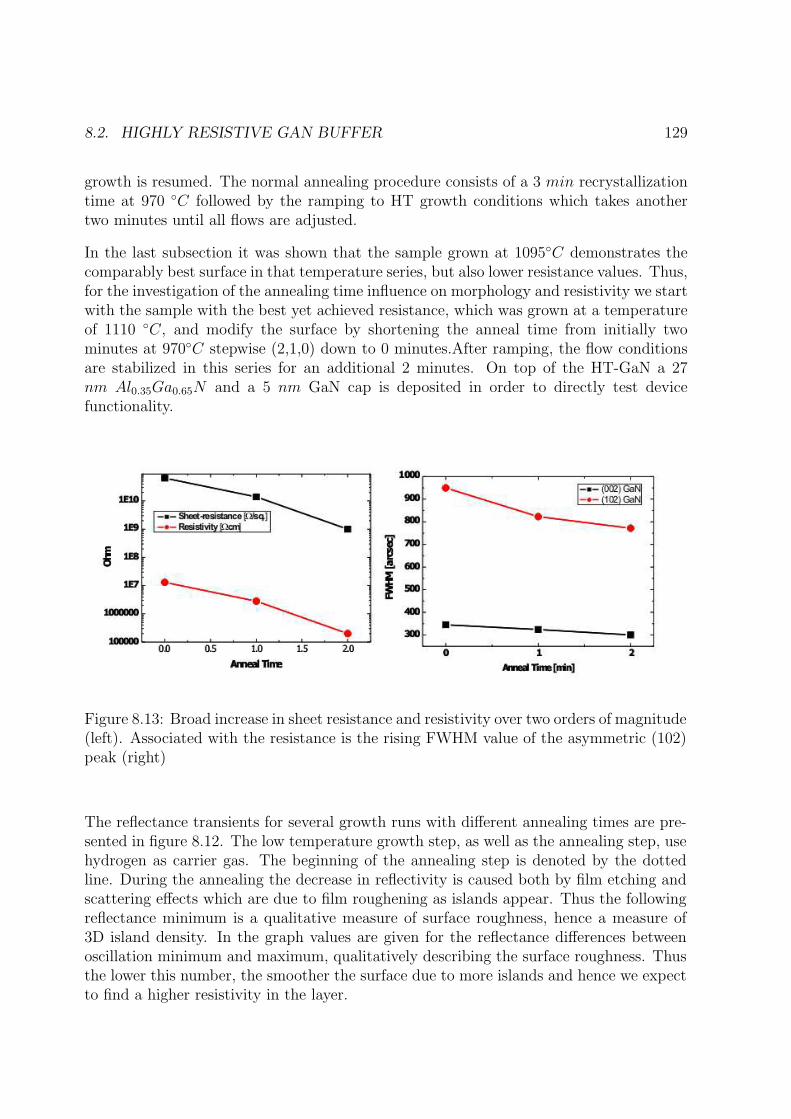
8.2. HIGHLY RESISTIVE GAN BUFFER 129
growth is resumed. The normal annealing procedure consists of a 3 min recrystallizationtime at 970 C followed by the ramping to HT growth conditions which takes anothertwo minutes until all flows are adjusted.
In the last subsection it was shown that the sample grown at 1095C demonstrates thecomparably best surface in that temperature series, but also lower resistance values. Thus,for the investigation of the annealing time influence on morphology and resistivity we startwith the sample with the best yet achieved resistance, which was grown at a temperatureof 1110 C, and modify the surface by shortening the anneal time from initially twominutes at 970C stepwise (2,1,0) down to 0 minutes.After ramping, the flow conditionsare stabilized in this series for an additional 2 minutes. On top of the HT-GaN a 27nm Al0.35Ga0.65N and a 5 nm GaN cap is deposited in order to directly test devicefunctionality.
Figure 8.13: Broad increase in sheet resistance and resistivity over two orders of magnitude(left). Associated with the resistance is the rising FWHM value of the asymmetric (102)peak (right)
The reflectance transients for several growth runs with different annealing times are pre-sented in figure 8.12. The low temperature growth step, as well as the annealing step, usehydrogen as carrier gas. The beginning of the annealing step is denoted by the dottedline. During the annealing the decrease in reflectivity is caused both by film etching andscattering effects which are due to film roughening as islands appear. Thus the followingreflectance minimum is a qualitative measure of surface roughness, hence a measure of3D island density. In the graph values are given for the reflectance differences betweenoscillation minimum and maximum, qualitatively describing the surface roughness. Thusthe lower this number, the smoother the surface due to more islands and hence we expectto find a higher resistivity in the layer.
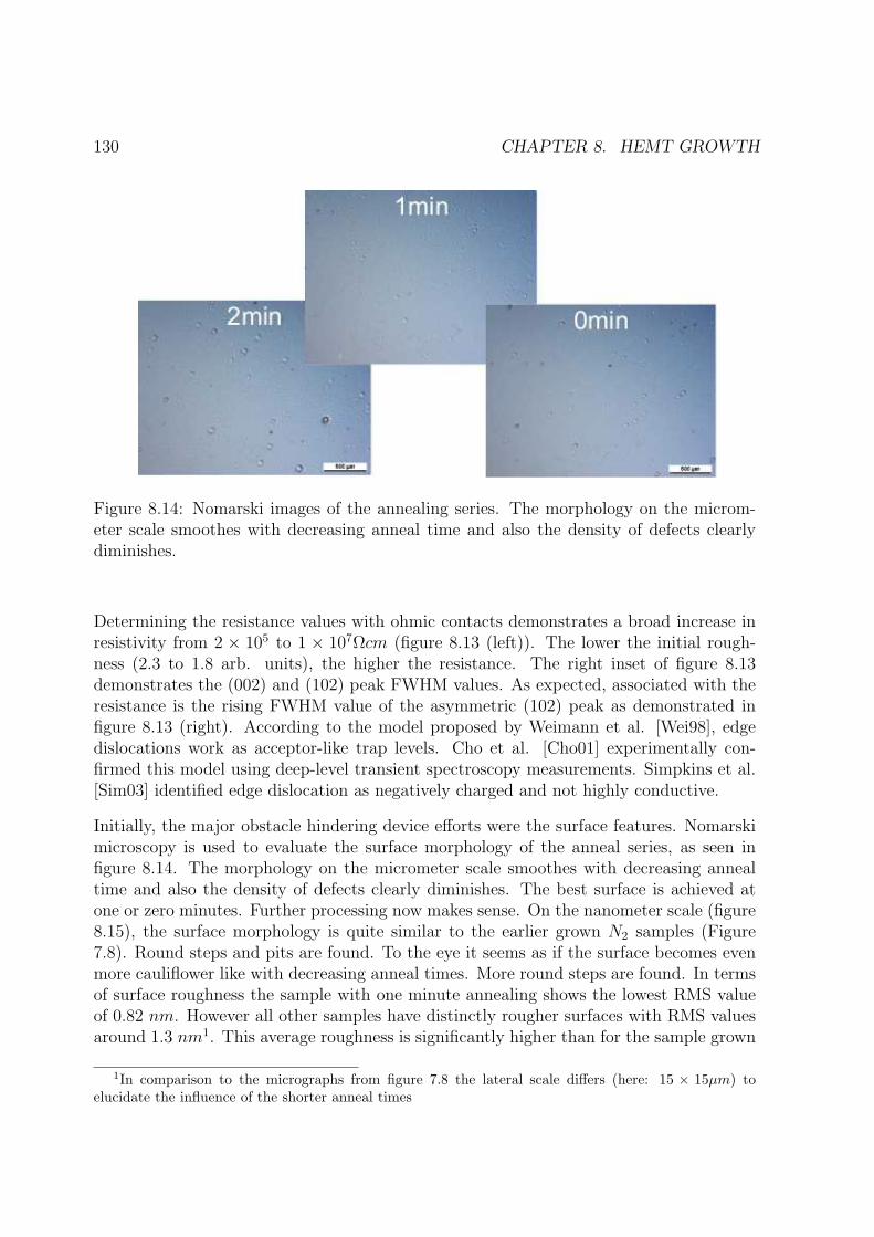
130 CHAPTER 8. HEMT GROWTH
Figure 8.14: Nomarski images of the annealing series. The morphology on the microm-eter scale smoothes with decreasing anneal time and also the density of defects clearlydiminishes.
Determining the resistance values with ohmic contacts demonstrates a broad increase inresistivity from 2 × 10⁵ to 1 × 10⁷Ωcm (figure 8.13 (left)). The lower the initial rough-ness (2.3 to 1.8 arb. units), the higher the resistance. The right inset of figure 8.13demonstrates the (002) and (102) peak FWHM values. As expected, associated with theresistance is the rising FWHM value of the asymmetric (102) peak as demonstrated infigure 8.13 (right). According to the model proposed by Weimann et al. [Wei98], edgedislocations work as acceptor-like trap levels. Cho et al. [Cho01] experimentally con-firmed this model using deep-level transient spectroscopy measurements. Simpkins et al.[Sim03] identified edge dislocation as negatively charged and not highly conductive.
Initially, the major obstacle hindering device efforts were the surface features. Nomarskimicroscopy is used to evaluate the surface morphology of the anneal series, as seen infigure 8.14. The morphology on the micrometer scale smoothes with decreasing annealtime and also the density of defects clearly diminishes. The best surface is achieved atone or zero minutes. Further processing now makes sense. On the nanometer scale (figure8.15), the surface morphology is quite similar to the earlier grown N2 samples (Figure7.8). Round steps and pits are found. To the eye it seems as if the surface becomes evenmore cauliflower like with decreasing anneal times. More round steps are found. In termsof surface roughness the sample with one minute annealing shows the lowest RMS valueof 0.82 nm. However all other samples have distinctly rougher surfaces with RMS valuesaround 1.3 nm1. This average roughness is significantly higher than for the sample grown
1In comparison to the micrographs from figure 7.8 the lateral scale differs (here: 15 × 15µm) toelucidate the influence of the shorter anneal times
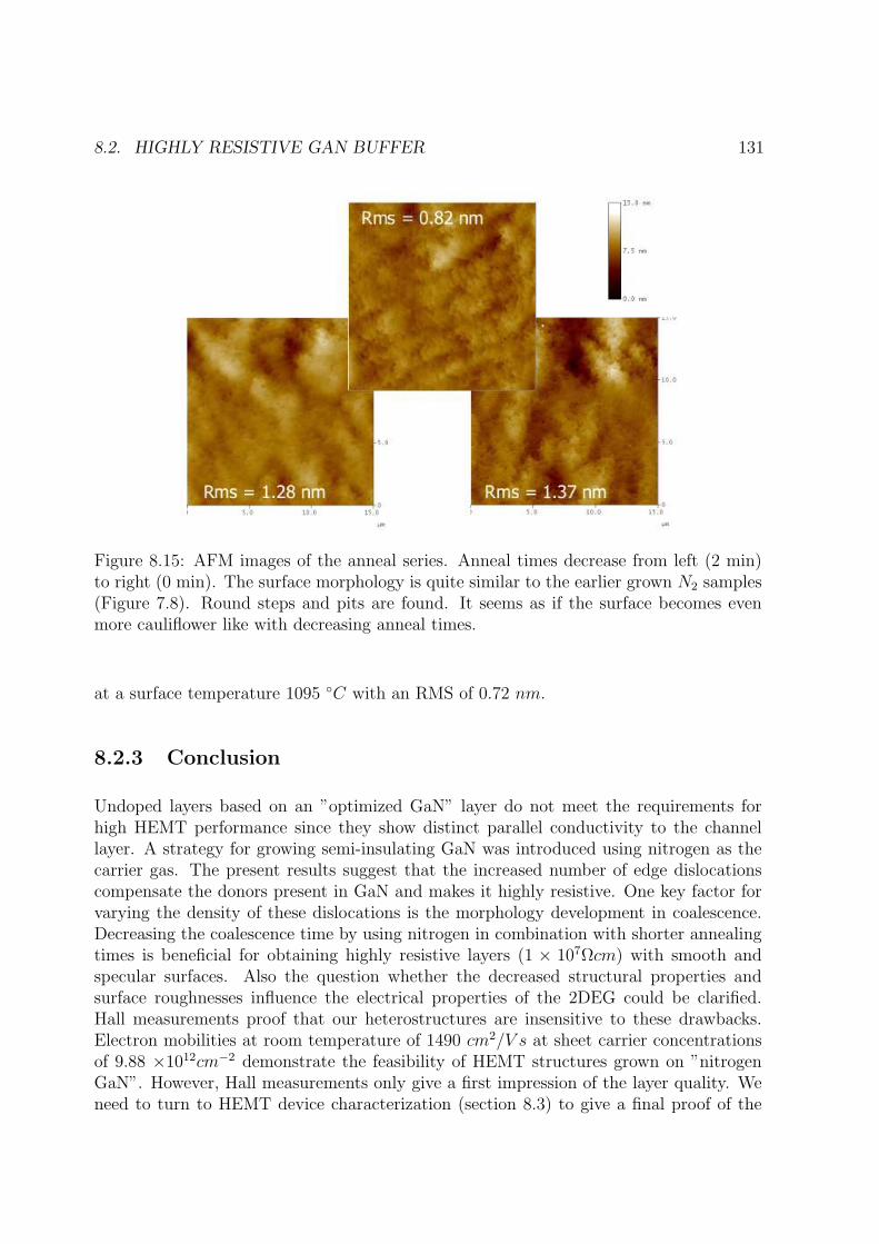
8.2. HIGHLY RESISTIVE GAN BUFFER 131
Figure 8.15: AFM images of the anneal series. Anneal times decrease from left (2 min)to right (0 min). The surface morphology is quite similar to the earlier grown N2 samples(Figure 7.8). Round steps and pits are found. It seems as if the surface becomes evenmore cauliflower like with decreasing anneal times.
at a surface temperature 1095 C with an RMS of 0.72 nm.
8.2.3 Conclusion
Undoped layers based on an ”optimized GaN” layer do not meet the requirements forhigh HEMT performance since they show distinct parallel conductivity to the channellayer. A strategy for growing semi-insulating GaN was introduced using nitrogen as thecarrier gas. The present results suggest that the increased number of edge dislocationscompensate the donors present in GaN and makes it highly resistive. One key factor forvarying the density of these dislocations is the morphology development in coalescence.Decreasing the coalescence time by using nitrogen in combination with shorter annealingtimes is beneficial for obtaining highly resistive layers (1 × 10⁷Ωcm) with smooth andspecular surfaces. Also the question whether the decreased structural properties andsurface roughnesses influence the electrical properties of the 2DEG could be clarified.Hall measurements proof that our heterostructures are insensitive to these drawbacks.Electron mobilities at room temperature of 1490 cm2/V s at sheet carrier concentrationsof 9.88 ×1012cm−2 demonstrate the feasibility of HEMT structures grown on ”nitrogenGaN”. However, Hall measurements only give a first impression of the layer quality. Weneed to turn to HEMT device characterization (section 8.3) to give a final proof of the

132 CHAPTER 8. HEMT GROWTH
feasibility of our growth approach.
8.3 HEMT results
The optimization of the GaN buffer and the AlGaN layer is successfully completed. How-ever its applicability with respect to HEMT device characteristics needs still to be proved.
RF-high-power HEMTs represent the application aim of our work. In contrast to smallsignal devices power HEMTs have gate lengths of 0.5 to 1 µm and cover areas of typ-ically several square-millimeter. These devices have to withstand a larger voltage andcurrent amplitude as compared to a small signal device, to provide high output power.Therefore the fulfillment of the -throughout this thesis- often mentioned requirements ofreproducibility, uniformity and material quality is paramount. To give a final proof of thefeasibility of our growth approach power HEMT devices were fabricated. In this sectionthe DC and RF characteristics of our grown heterostructures are discussed.
The HEMT is a three terminal device (as seen in figure 8.16) and is geometrically char-acterized by the gate length Lg, the gate width Wg, and the Source-Drain distance S D.The current flow in between the contacts is controlled by a bias voltage through the mid-dle Schottky contact (Gate). The standard HEMT processing procedure requires severallithographic steps and consists of the mesa etching, the fabrication of ohmic and Schottkycontacts for the source/drain contacts and the gate respectively. Further details aboutHEMT processing can be found in [Ber05]. It is worth noticing that the fabricated devicesare unpassivated.
Figure 8.16: Schematic drawing of a HEMT structure (left) and a real processed HEMT(right).
The layer stack consists of a 2.5 µm thick undoped GaN buffer followed by a 27 nm thinAl0.35Ga0.65N layer covered by a 4 nm GaN cap as determined via RBS. We compare

8.3. HEMT RESULTS 133
samples with different buffer resistivity values of 3 × 10⁵ and 1 × 10⁷Ωcm and otherwiseidentical heterostructure. The latter sample originates from the ”annealing time” seriesin section 8.2.2 with 0 minutes annealing at 970 C.
Hall measurements at room temperature reveal mobilities of 1405 and 1093 cm2/V s atsheet carrier concentrations of 8.2 and 8.7 × 1012 cm−2, respectively. The difference isnot necessarily originating from the different layer characteristics, but due to the appliedand rather simplistic alloying procedure based on indium contacts. Moreover the secondmeasured sample is cut from near the wafer edge since the middle was used for the HEMTprocessing.
Measurements of the output and the transfer characteristics are one of the basic methodsfor HEMT characterization. Using these measurements the functionality of the deviceand the quality of the layer structure can be analyzed. All measurements are performedby means of an Agilent E5270A semiconductor analyzer. The measurement system al-lows to measure in a bias range of -200 to +200 V . The current range is up to 1Awith femto-ampere accuracy. The gate-source and the drain-source biases are controlledsimultaneously and the gate and drain currents are read subsequently.
V =1...-7V
W = 200µm
L=0.9nm
gs
g
g
0 5 10 150.00
0.20
0.40
0.60
0.80
1.00
1.20
Dra
incurr
ent
(A/m
m)
Drain-source bias (V)
1068 M14k dc
0 5 10 150.00
0.20
0.40
0.60
0.80
1.00
1.20
Dra
incurr
ent
(A/m
m)
Drain-source bias (V)
1076 L14k dc
V =1...-7V
W = 200µm
L=0.9nm
gs
g
g
Figure 8.17: DC output characteristics for a gate bias from 1 to -7 V of two samplesgrown on different GaN buffers. Lg = 0.9 µm; Wg = 200 µm
From measurements one can extract the maximum drain current Isatd , the threshold voltage
Vth, the extrinsic transconductance gm and gate leakage currents. The typical output andtransfer characteristics measured for both samples are shown in figure 8.17 for gate widthof 200 µm, a gate length of 0.9 µm and a source drain distance of 3 µm (two finger device).In either transistor structure a decreasing drain current is measured in the saturationregion with increasing drain-source bias. The origin of this negative resistance effect hasbeen attributed to self heating of the device due to the poor thermal conductivity ofthe sapphire substrate [Ber03]. This effect can thus only be reduced by using differentsubstrates. The output characteristics shown in figure 8.17 exhibit a saturation draincurrent of 0.78 and 0.68 A/mm respectively. The origin of this slight difference can only bespeculated upon. Further measurements will be necessary. It is reasonable to assume that

134 CHAPTER 8. HEMT GROWTH
-8 -7 -6 -5 -4 -3 -2 -1 0 10
50
100
150
200
0.00
0.05
0.10
0.15
0.20
gm(m
S/m
m)
gate-source bias (V)
Vth
= - V1076-1 L14k dc
dra
incurr
ent
(A)
-8 -7 -6 -5 -4 -3 -2 -1 0 10
50
100
150
200
0.00
0.05
0.10
0.15
0.20
gm(m
S/m
m)
gate-source bias (V)
Vth
= - V1068 M14k dc
dra
incurr
ent
(A)
Figure 8.18: Transfer characteristics of the HEMT structures.
device manufacturing instead of intrinsic material properties accounts for the difference.Other origins of this difference may be the dependency of Id on the mobility, electronvelocity and carrier concentration. However, since RBS of these samples demonstratedidentical structures and compositions at least a change in the carrier concentration canbe excluded.
Extrinsic transconductances of 160 and 130 mS/mm at a threshold voltage of -5.5 Vare measured for the devices as seen in figure 8.18. These results are comparable withpublished results of AlGaN/GaN/Sapphire HEMTs where Isat
d reaches from 0.46A/mm to0.95A/mm and gm from 150 mS/mm to 236 mS/mm [Jav03, Gre00, Chi03, Dav04, Joh01].The gate leakage currents were measured to be 1 and 0.1 µA at Vgs = -6 V and Vds = 0V ,respectively.
Boundary frequencies are important for RF characterization. These parameters provethe device capability to operate at high frequencies or with high switching speeds. Tocharacterize the frequency behavior two basic parameters are used in practice: The currentgain cutoff frequency (or transit frequency) fT and the maximum frequency of oscillationfmax, which define the frequency range where the HEMT shows amplifying behavior.The boundary frequencies were evaluated from s-parameter measurements in a frequencyrange up to 110GHz using a HP 8510C Network Analyzer. Devices were measured for gatesource bias in a range from +1 V to Vth and drain source bias in a range from 0 to 20 V .To be comparable to HEMT results from GaN on SiC, which were processed in our labsbefore, the GaN on sapphire devices were measured at comparable working points (Vgs
=-2.5 V and Vds=20 V ). The devices with a gate length of Lg = 0.9 µm showed a cutofffrequency of fT = 6.5 and 11.2 GHz respectively and a maximum frequency of oscillationof 20 and 18.9 GHz. Our HEMTs on SiC substrates show similar cutoff frequencies (∼ 10GHz for fT ). Since the frequencies are working point and HEMT geometry dependent aworking point more suitable for high transit frequencies (Vgs =-5 V and Vds=20 V ) showsa ft value of 14.1 and 13.3 GHz respectively. These results are also comparable to otherpublished values of AlGaN/GaN/Sapphire HEMTs [Jav03].

8.3. HEMT RESULTS 135
These findings finally prove the functionality and feasibility of our MOVPE growth pro-cess. Moreover the output and RF characteristics are comparable to HEMT results ofGaN on SiC produced at our institute [Heid06]. Thus we are able to fabricate GaN-basedHEMT devices with state of the art electrical characteristics using the new growth processapproaches.

136 CHAPTER 8. HEMT GROWTH

Chapter 9
Summary and Conclusions
Research aim of this work was to develop an MOVPE based growth process that allowsthe reliable and efficient deposition of high quality material for HEMT devices based onAlGaN/GaN heterojunctions. The main task was to establish a broad comprehension ofthe epitaxial process based on numerical and experimental data and eventually to prove itsfunctionality in terms of HEMT characteristics. On account of this, several requirementsfor suitable power HEMT material were derived in this work:
• Reproducible layer growth
Usage and development of adequate growth control and monitoring instruments is essen-tial to meet these premises. It was shown that direct wafer surface temperature deter-mination is a must during growth, though it is challenging for transparent substrates.Emissivity corrected pyrometry is a widely employed tool for surface temperature mea-surements. However, commonly applied calibration methods for absolute temperaturedetermination of the wafer surface can be erroneous when based on phase transition ormelting point observations. Therefore, a new calibration method for transparent sub-strates has been demonstrated by using the in-situ measured, temperature dependent andband-gap related reflectance shift of SiC. This new approach for temperature determi-nation makes growth conditions on transparent substrates comparable, independent ofthe reactor type used. Moreover and more importantly for the following discussion, thistechnique allows to adjust the MOVPE system to identical run-by-run wafer tempera-tures. A reliable basis for absolute temperature determination is established. Using thisnew temperature determination approach the cause of irreproducibility in an horizontalreactor is investigated. Parasitic deposits that form on the cold reactor walls and insuf-ficient temperature control (the one allowing for the other) are the two major origins ofirreproducibility.
137

138 CHAPTER 9. SUMMARY AND CONCLUSIONS
A new deposition approach is introduced that reduces the formation of parasitic deposi-tions on the reactor walls, by injecting the metalorganics near the substrate unlike theconventional process. Experiment and modelling verify the suitability of the new growthapproach for enhanced reproducibility. Moreover the new approach leads to a fourfoldreactor uptime without changing reactor quartz parts. The structural, morphological andelectrical characteristics of the grown layers are comparable for both processes.
• ”Manufacturing uniformity” in terms of a high yield of homogenous layer charac-teristics
Homogeneity in terms of thickness and epilayer characteristics was addressed next. It hasbeen found that inversion of the precursor supply has a drawback when considering thethickness uniformity. In order to achieve a homogeneous distribution of growth speciesover the substrate flow mechanical aspects in our reactor system are investigated. Thegas velocity as well as the gas ”nature” are therefore important optimization parameters.For that purpose the role of different carrier gases - nitrogen and hydrogen - on III-nitridegrowth is examined. Using the inverted inlet configuration, uniformity can only be im-proved by changing the nature of the carrier gas, thus, modifying the diffusive transportand decomposition of growth species Thus, the growth species are distributed more uni-formly above the susceptor. This way, in N2 atmosphere a standard deviation in thicknessof less than 3% is achieved in comparison to 10% for H2 ambient. Further investigationsare necessary to understand the influence of the nitrogen carrier gas on GaN epilayerscharacteristics.
• Structural quality with low dislocation densities and a smooth, defect free surface
Nitrogen is crucial for improved thickness homogeneity, but apparently nitrogen not onlydeteriorates the surface morphology but it affects the growth mode in the early stages ofdeposition. From the presented data it is found that untimely recovery of the reflectancesignal, i.e. start of 2D growth, leads to GaN layers which contain a larger number ofedge type dislocations. Dislocations, in turn, influence the strain in the layer, leading tomore relaxed GaN layers when grown in nitrogen ambient. Dislocation scattering is thevery probable source of the decline in electrical data when nitrogen is used as carrier gas.As a result a larger ”coalescence thickness” is preferred, since it reduces the density ofdislocations. Therefore a strategy was developed with which good quality material canbe obtained despite the nitrogen ambient needed for uniform layers.
State of the art electrical and structural quality material as well as uniform layers withsmooth surfaces were achieved by using only small amounts of hydrogen (∼ 15%) duringthe coalescence phase in otherwise nitrogen ambient. We managed to even increase theHall mobility at room temperature up to 671 cm2/Vs with a carrier concentration of

139
9 × 1016cm−3 and a FWHM for the (002) and (102) reflections of 238 and 349 arcsecrespectively at a standard deviation in thickness of 3%. In this way, a high quality GaNtemplate is produced. Further investigation are carried out to check the suitability as abuffer for HEMTs.
• Tight alloy composition and thickness control in the heterostructure
AlGaN was grown on top of the high quality GaN template with the main focus on con-trolled Aluminium content and studies were performed regarding the abrupt- and smooth-ness of the heterostructure interface. The inverted inlet combines the reproducibility of thegrowth process with a good growth control for AlxGa1−xN . Due to the high incorporationefficiency a minimal amount of adduct formation occurred. Tight alloy composition andthickness control was achieved with less than one percent deviation over the wafer fordevice relevant aluminum contents in either hydrogen and nitrogen as carrier gas. Al-GaN/GaN heterostructures were grown on the ”optimized GaN”. Despite state of theart sheet conductivity values (1.92 ×10¹⁶V
−1s−1) the heterojunctions exhibit additionalconductivity due to residual donors in the layer. That way we measured a resistivity ofless than 1 Ωcm in the GaN. In a device structure we found considerable parallel conduc-tion effects leading to unsatisfactory device pinch off. Therefore resistance control wasaddressed next to achieve high quality HEMT devices.
• Semi-insulating GaN layers
A strategy for growing semi-insulating GaN was introduced using nitrogen as the carriergas. The present results suggest that the increased number of edge dislocations compen-sates GaN and makes it highly resistive. One key factor for varying the density of thesedislocations is the morphology development in coalescence. Decreasing the coalescencetime by using nitrogen in combination with shorter annealing times is beneficial for ob-taining high resistive layers (1 × 10⁷Ωcm) with smooth and specular surfaces. Also thequestion whether the decreased structural quality and surface roughnesses influence theelectrical properties could be clarified. Electron mobilities at room temperature of 1490cm2/V s at a sheet carrier concentrations of 9.88 ×1012cm−2 demonstrate the suitabilityof HEMT structures grown on ”nitrogen GaN”.
The output and RF characteristics of the produced HEMT structures are comparable toHEMT results of GaN on sapphire (and even GaN on SiC, produced at our institute),with values for Isat
d of ∼ 0.7 A/mm and gm of ∼ 150 mS/mm and cutoff frequencies ∼11 GHz for the chosen geometry and working point. These findings finally prove thefunctionality and feasibility of our MOVPE growth process.
Thus, new holistic approaches to III-nitride monitoring and growth are presented. Highreliability, reproducibility and minimum downtimes of the equipment is proven, optimized

140 CHAPTER 9. SUMMARY AND CONCLUSIONS
AlGaN/GaN film deposition shown and transferability of process temperatures to anyreactor demonstrated.
Bibliography
[Aka89] I. Akasaki and H. Amano and Y. Koide and K. Hiramatsu and N. Sawaki, J.Crystal Growth, 98, 209 (1989).
[Amb98] O. Ambacher, J. Phys. (D): Appl. Phys., 31, 2653, 1998.
[Amb99] O. Ambacher, J. Smart, J.R. Shealy, N.G. Weimann, K. Chu, M. Murphy, W.J.Schaff, L.F. Eastman, J. Appl. Phys., 85, No. 6, 3222, 1999.
[Amb00] O. Ambacher, B. Foutz, J. Smart, J.R. Shealy, N.G. Weimann, K. Chu, M.Murphy, A.J.Sierakowski, W.J. Schaff, L.F. Eastman, J. Appl. Phys., 87, No. 1,334, 2000.
[Ama84] H. Amano, N. Sawaki, and I. Akasaki, J. Crystal Growth, 68, 163 (1984).
[Ama86] H. Amano, N. Sawaki, I. Akasaki, Y. Toyoda, Apppl. Phys. Lett., vol. 48, 353(1986).
[Ama98] H. Amano and M. Iwaya and T. Kashima and M. Katsuragawa and I. Akasakiand J. Han and S. Hearne and J.A. Floro and E. Chason and J. Figiel, Jpn. J.Appl. Phys., 37, L1540 (1998)
[Asp95] D.E. Aspnes, Mater. Sci. Eng. B 30 (1995) 10
[Bal03] R.S. Balmer and T. Martin, J. Crystal Growth 48 (2003), p. 216
[Bea01] B. Beaumont and Ph. Vennegues and P. Gibart, phys. stat. sol. (b), 227, 1 (2001)
[Ben68] S.W. Benson, Thermochemical Kinetics, John Wiley and Sons, 1st ed., 1968
[Ben82] S.W. Benson, The Foundation of Chemical Kinetics, Robert E. Krieger, Malabar,Florida, 1982
[Ber05] J. Bernat, Fabrication and Characterisation of AlGaN/GaN High Electron Mo-bility Transistors for Power Applications, Dissertation, RWTH Aachen, 2005
141

142 BIBLIOGRAPHY
[Ber03] M.Berroth, E.Chigaeva, I. Dettmann, T. Stumpf, AlGaN/GaN - Heterostruk-turfeldeffekttransistoren Eigenschaften und Anwendungen, EEEfCOM 2003, Ulm(2003)
[Bin86] Binnig, G., Quate, C.F., and Gerber, Ch., Atomic force microscope, Phys. Rev.Lett. 56(9), 930-933, 1986
[Bir60] R. Bird, W. Stewart, E. Lightfoot, Transport Phenomena, John Wiley and SonsNew York, 1960
[Bob94] F.G. Bobel, A. Wowchak, P.P. Chow, J. Van Hove, L.A. Chow, Mater. Res. Soc.Symp. Proc. (1994) 105.
[Bor80] M. Born, E. Wolf, Principles of Optics, Pergamon Press, 1980
[Bot01] T. Bottcher, S. Einfeldt, S. Figge, R. Chierchia, H. Heinke, J. S. Speck and D.Hommel, Applied Physics Letters, 78, 1976 (2001)
[Car94] J.O. Carlson, Chemical Vapor Deposition; in Handbook of Deposition Technolo-gies for Films and Coatings, Noyes Publications, 1994
[Chi03] A.Chini, R.Coffie, G.Meneghesso, E. Zanoni, D.Buttari, S. Heikman, S.Keller,U.K.Mishra, 2.1A/mm current density AlGaN/GaN HEMT, Electron. Lett. 39(2003)
[Cho01] H.K. Cho, K.S. Kim, C.H. Hong and H.J. Lee, J. of Crystal Growth, 223, 38(2001).
[Cho06] Y. S. Cho, H. Hardtdegen, N. Kaluza, N. Thillosen, R. Steins, Z. Sofer, and H.Luth, phys. stat. sol. (c), in press 2006.
[Cui00] J. Cui et al.,MRS J. Nitride Semicond. Res. 5, 7, (2000).
[Dat04] R. Datta, M.J. Kappers, M.E. Vickers. J.S. Barnard, C.J. Humphreys , Super-lattices and Microstructures, 36, 393 (2004).
[Dau98] I. Daumiller, C. Kirchner et al., Device Research Conference Digest, pp. 114-115,1998.
[Dau01] M. Dauelsberg, H. Hardtdegen, L. Kadinski, A. Kaluza, P. Kaufmann, J. Cryst.Growth, 223, 21, 2001
[Dav04] S.K.Davidsson, M.Gurusinghe, T. G.Andersson, H. Zirath, Journal of Electron.Mater. 33, 440 (2004).
[Eas02] L.F. Eastman, U.K. Mishra The Toughest Transistor Yet ; IEEE Spectrum, pp.28-33, (2002).

BIBLIOGRAPHY 143
[Edg94] J.H. Edgar Properties of Group III Nitrides,INSPEC, 1994.
[Fig00] S. Figge, T. Bottcher, S. Einfeldt and D. Hommel, J. Cryst. Growth, 221, 262(2000).
[Fou03] B.Foutz, http://iiiv.tn.cornell.edu/www/foutz/nitride.html
[Gil86a] L.J. Giling, J. van de Ven, in Advanced Crystal Growth, Chpt. 12, Prentice HallInt., 1986.
[Gil86b] L.J. Giling, J. van de Ven, The Physics of CVD Processes, 1986.
[Gil98] B. Gil, Group III Nitride Semiconductor Compounds: Physics and Applications,Oxford University Press, 1998
[Gre00] B.M.Green, K. K.Chu, E.M.Chumbes, J. A. Smart, J. R. Shealy, L. F. Eastman,The Effect of Surface Passivation on the Microwave Characteristics of UndopedAlGaN/GaN HEMT’s, IEEE Electr. Device L. 21, 268 (2000)
[Grz05] A.P. Grzegorczyk, L. Macht, P.R. Hageman, J.L. Weyher and P.K. Larsen, J. ofCrystal Growth, 273, 424 (2005).
[Hab02a] K. Haberland et al., J. Cryst. Growth , 207, 87, 2002
[Hab02b] K. Haberland, A. Kaluza, M. Zorn, M. Pristovsek, H. Hardtdegen, M. Weyers,J.-T. Zettler, W. Richter, J. Crystal Growth 240, 87 (2002).
[Hab02] K. Haberland, Optical in-situ Studies during MOVPE with respect to III-V deviceproduction, Dissertation, TU Berlin, 2002
[Had90] H.-F. Hadamovsky, Werkstoffe der Halbleitertechnik, VEB Deutscher Verlag furGrundstoff Industrie, Leipzig (1990).
[Hal79] E.H. Hall, New Action of the Magneton Electric Currents, Amer. J. Math. 2(1879), p. 287 ff.
[Hal01] I. Halidou, T. Boufaden, A. Touhami, A. Rebey, B.E. Jani, Physica Status SolidiA, 184, 263 (2001)
[Han97] J. Han, T.-B. Ng, R.M. Biefeld, M.H. Crawford, D.M. Follstaedt, Appl. Phys.Lett., 71, No. 21, 3114, 1997
[Har01] H. Hardtdegen, A. Kaluza, D. Gauer, M. v. d. Ahe, M. Grimm, P. Kaufmann,and L. Kadinski, J. Cryst. Growth, 223, 15 (2001).
[Har03] H. Hardtdegen, CVD Processes, Fundamentals of Nanoelectronics, 34th IFFSpring School 2003

144 BIBLIOGRAPHY
[Har04] H. Hardtdegen, N. Kaluza, R. Steins, R. Schmidt, K. Wirtz, E.V. Yakovlev, R.A.Talalaev, Yu.N. Makarov, J. of Crystal Growth, 272, 407 (2004)
[Har04a] H. Hardtdegen, N. Kaluza, R. Schmidt, R. Steins, E.V. Yakovlev, R.A. Talalaev,Yu.N. Makarov, J.-T. Zettler, Phys. Stat. Sol. (a) 201 (2004) 312.
[Hei01] K. Heime, Elektronische Bauelemente; Institut fur Halbleitertechnik - LehrstuhlI, Vorlesung an der Rheinisch-Westfalischen Technischen Hochschule Aachen,2001
[Hei02] S. Heikman, S. Keller, S.P. DenBaars, U.K. Mishra, Applied Physics Letters, 81,439 (2002).
[Heid06] G. Heidelberger, A. Fox, M. Marso, Institut fur Schichten und Grenzflachen,private communication 2006
[Hey96] B. Heying, X. H. Wu, S. Keller, Y. Li, D. Kapolnek, B. P. Keller, S. P. DenBaars,and J. S. Speck, Appl. Phys. Lett. 68, 643 (1996).
[Hey99] B. Heying, E. J. Tarsa, C. R. Elsass, P. Fini, S. P. DenBaars, and J. S. Speck,Journal of Applied Physics, 85, 6470 (1999).
[Hir86] K.Hirakawa, H. Sakaki, Phys. Rev. B 33, 8291 (1986)
[Hir97] K. Hiramatsu and T. Detchprohm and H. Amano and I. Akasaki, Effects of bufferlayers in heteroepitaxy of gallium nitride, T. Nishinaga, K. Nishioka, J. Harada,A. Sasaki and H. Takei (Editors), Elsevier Science B.V., Amsterdam, 1997
[Hol96] M. Hollfelder, Dissertation, RWTH Aachen, 1996
[Hwa97] C.Y. Hwang, M.J. Schurman, W.E. Mayo, Y.C. Lu, R.A. Stall, and T. Salagaj,J. electron. Mater., 26, 243 (1997).
[Iba99] H. Ibach, H. Luth, Festkorperphysik: Einfuhrung in die Grundlagen, Springer-Verlag, 1999
[Jav02] P. Javorka, A. Alam, M. Wolter, A. Fox, M. Marso, M. Heuken, H. Luth, and P.Kordos, IEEE Electron Device Lett. 23, 287 (2002).
[Jav03] P. Javorka, Fabrication and Characterisation of AlGaN/GaN High Electron Mo-bility Transistors, Dissertation, RWTH Aachen, 2003.
[Jen01] D. Jena, Y. Smorchkova, Ch. Elsass, A. C.Gossard, and U.K.Mishra, Electrontransport and intrinsic mobility limits in two-dimensional electron gases of III-V nitride heterostructures, American Physical Society March Meeting, Seattle,Washington (2001).
[Jen93] K.F. Jensen, Chemical Vapor Deposition, Chpt. 2, Academic Press, 1993.

BIBLIOGRAPHY 145
[Jen94] K.F. Jensen, in Handbook of Chrystal Growth 3b, Thin Films and Epitaxy, Chpt.13, Elsevier Science B.V., 1994
[Joh93] S.R. Johnson, C. Lavoie, T. Tiedje and J.A. Mackenzie, J. Vac. Sci. Technol. B.11 (1993) (3).
[Joh01] J.W. Johnson, A.G.Baca, R.D.Briggs, R. J. Shul, J. R.Wendt, C.Monier,F.Ren, S. J. Pearton, A.M.Dabiran, A.M. Wowchack, C. J. Polley, P. P.CHow,Solid-State El. 45, 1979 (2001).
[Jon00] L.L. Jones and P.W. Atkins,Chemistry: Molecules, Matter, and Change, W.H.Freeman and Co., New York, 2000.
[Kal03] N. Kaluza, MOVPE Growth and Characterization of AlGaN/GaN Heterostruc-tures for HEMT Application, PhD Thesis, RWTH Aachen, 2003
[Kal04] N. Kaluza, R. Steins, H. Hardtdegen and H. Lueth, J. of Crystal Growth, 272,407 (2004)
[Kel95] B. P. Keller et al., Metalorganic chemical vapor deposition growth of high opticalquality and high mobility GaN, J. Electron. Mater., 24, 1707 (1995).
[Kel01] S. Keller, Wu Yi-Feng, G. Parish, Ziang Naiqian, J.J. Xu, B.P. Keller, S.P.DenBaars, U.K. Mishra, IEEE Transactions on Electron Devices, 48, 552 (2001).
[Kir59] G. Kirchhoff. Mber. Akad. Wiss. Berlin, Dez. 1859 (s. in Gesammelte Abhand-lungen. Barth, Leipzig 1882, S. 566).
[Kle95] C.R. Kleijn, Chemical Vapor Deposition Processes ; in Computational Modelingin Semiconductor Processing, Artech House, 1995
[Kol04] D.D. Koleske, M.E. Coltrin, K.C. Cross, C.C. Mitchell, A.A. Allerman, J. ofCrystal Growth, 273, 86 (2004)
[Kro05] A. Krost, F. Schulze, A. Dadgar, G. Strassburger, K. Haberland, T. Zettler,Physica Status Solidi B, 242, no.13, 2570 (2005).
[Lant00] R. Lantier, GaN/Al(Ga)N Heterostructures: MBE Growth,Electronic Propertiesand Polarization Fields, PhD Thesis, RWTH Aachen, 2000
[Li04] D. Li, H. Chen, H.B. Yu, Y.J. Han, X.H. Zheng, Q. Huang, J.M. Zhou, J. ofCrystal Growth, 263, 76 (2004).
[Liu78] S. Liu and D. Stevenson, J. Electrochem. Soc. 125, 1161 (1978).
[Liu02] L. Liu, J.H. Edgar, Materials Science and Engineering, R 37, 61, 2002
[Man69] H. Manasevit, W. Simpson, J. Electrochem. Soc., 116, 1725, 1969

146 BIBLIOGRAPHY
[Mih99] T. Mihopoulus, Ph. D Thesis, Massachusetts Institute of Technology, 1999
[Moo78] W.J. Moore, Physical Chemistry, Longman Group Ltd., 1978
[Mor98] H. Morkoc, Nitride Semiconductors and Devices, Springer Series in MaterialScience, 1998
[Muk98] T. Mukai, H. Narimatsu, and S. Nakamura, Jpn. J. Appl. Phys., 37, L479 (1998).
[Mul05] S. Muller, K. Kohler, R. Kiefer, R. Quay, M. Baeumler, L. Kirste, Physica StatusSolidi C, 7, 2639 (2005),
[Nag80] B.R.Nag, Electron Transport in Compound Semiconductor, Springer-Verlag edi-tion (1980)
[Ng98] H.M. Ng and D. Doppalapudi and T.D. Moustakas and N.G. Weimann and L.F.Eastman, Appl. Phys. Lett., 73, 821 (1998)
[Nak91] S.Nakamura, Jpn J. Appl. Physics 30, (10A):L1705, 1991
[Nak91a] S. Nakamura, Y. Harada, M. Senoh, Appl. Phys. Lett., 58, 2021 (1991).
[Nak92] S. Nakamura, T. Mukai, and M. Senoh, J. Appl. Phys., 71, 5543 (1992).
[Nak99] S. Nakamura, M. Senoh, S. Nagahama, T. Matsushita, H. Kiyoku, Y. Sugimoto,T. Kozaki, H. Umemoto, M. Sano, and T. Mukai, Jpn. J. Appl. Phys., 38, L226(1999).
[Ogi80] T. Ogino and M. Aoki, Jpn. J. Appl. Phys, 19, 2395 (1980).
[Ois03] Toshiyuki Oishi, Naruhisa Miura, Muneyoshi Suita, Takuma Nanjo, Yuji Abe,and Tatsuo Ozeki, Hiroyasu Ishikawa, Takashi Egawa, and Takashi Jimbo, Jour-nal of Applied Physics, 94, 1662 (2003).
[Pau58] L.J. van der Pauw, Phillips Research Reports, 13:1ff (1958)
[Pie92] H.O. Pierson, Handbook of Chemical Vapor Deposition (CVD) (Noyes Publica-tions, Park Ridge NJ, 1992)
[Pla00] M. Planck, Verh. Dtsch. Phys. Ges. Berlin 2 (1900) 202, 237.
[Fan03] Fan Ren, John C. Zolper, Wide energy bandgap electronic devices, Singapore :World Scientific , 2003
[Ric86] W. Richter, Festkorperprobleme 26, 335, 1986
[Riz00] A.Rizzi, R. Lantier, and H. Luth, Phys. Status Solidi A 177, 165 (2000)
[Sch03] H.P.D. Schenk, P. Vennegues. O. Tottereau, T. Rieman, J. Christen, J. of CrystalGrowth, 258, 232 (2003)

BIBLIOGRAPHY 147
[Sch03a] C. Schaefer, Diplomarbeit, RWTH Aachen, IHT, 2003
[Shi04] E. Shimizu, S. Sugawara, and H. Nakata, J. Cryst. Growth, 266, 340 (2004).
[Smo99] I. P. Smorchkova, C.R. Elsass, J. P. Ibbetson, R.Ventury, B.Heying, P. Fini,E.Haus, S. P.DenBaars, J. S. Speck, U.K. Mishra, J. Appl. Phys. 86, 4520 (1999)
[Sha75] D.W. Shaw, J. Cryst. Growth 31, 30 (1975)
[Sim03] B.S. Simpkins, E.T. Yu, P. Waltereit and J.S. Speck, J. Appl. Phys., 94, 1448(2003).
[Ste03] R. Steins, Metalorganic Vapour Phase Epitaxy of and Characterization of GaN,RWTH Aachen, Diplomarbeit, 2003
[Str99] G.B. Stringfellow, Organometallic Vapor-Phase Epitaxy: Theory and Practice(Academic Press Inc., 2nd ed. San Diego 1999)
[Str01] G.B. Stringfellow, Mater. Sci. Eng. B, 87, 97 (2001)
[Sze81] S.M. Sze, Physics of Semiconductor Devices, 2.Auflage, John Wiley & Sons, 1981
[Tim92] P.J. Timans, J. Appl. Phys 72 (1992) (2).
[Thi02] N. Thilossen, Optische Charakterisierung von Nitriden hergestellt mittelsMOVPE, Diplomarbeit, RWTH Aachen, 2002
[Var67] Y. P. Varshni, Physica (Amsterdam) 34, 149 (1967)
[Wan01] H. X. Wang, Y. Amijima, Y. Ishihama, and S. Sakai, J. Crystal Growth, 233,681 (2001).
[Wei98] N.G. Weimann, L.F. Eastman, D. Doppalapudi, H.M. Ng and T.D. Moustakas,J. Appl. Phys., 83, 3656 (1998).
[Wic04] A. E. Wickenden, , D. D. Koleske1, R. L. Henry, M. E. Twigg and M. Fatemi,J. of Crystal Growth, 260, 54 (2004).
[Yan00] T. Yang. K. Uchida, T. Mishma, J. Kasai and J. Gotoh, phys. stat. sol. (a), 180,45 (200)
[Yos83] S. Yoshida, S. Misawa, and S. Gonda, Appl. Phys. Lett. 42, 427, 1983
[Zha99] Y. Zhang, J. Singh, J. Appl. Phys. 85, 587 (1999)
[Zet98] J.-T. Zettler et. al., J. of Crystal Growth, 195, 151, 1998
[Zhe99] T.S. Zheleva and S.A. Smith and D.B. Thomson and K.J. Linthicum and P.Rajagopal and R.F. Davis, J. Electron. Mater., 28, L5 (1999)

148 BIBLIOGRAPHY
[Zor95] M. Zorn, J. Jonsson, W. Richter, J.-T. Zettler and K. Ploska, phys. stat. sol. (a)152, 23, 1995

149
DanksagungLicht und Finsternis sind nicht unvereinbar, sondern wohlbekannte Teile eines großerenGanzen.
Mit allen unseren Ecken und Kanten, mit der uns eigenen Veranlagung, unserem Wesenund Charakter, mit allen unausgeglichenen und spitzen Stellen, mit denen wir so haufiganecken, gleichen wir dem symbolhaften unbehauenen Stein. Er muß innerlich von unsbearbeitet werden. In diesem Sinne mochte ich mich bei all jenen bedanken, die diesemStein ein wenig Form gegeben haben:
• Herrn Prof. Dr. H. Luth, der mir die Moglichkeit gab, diese Arbeit am Institut furSchicht- und Grenzflachen des Forschungszentrums Julich anzufertigen,
• Prof. Dr. Wilfried Mokwa fur die Ubernahme des Koreferats. Daruberhinaus dankeich auch fur die Moglichkeit der langjahrigen Mitarbeit als Hiwi an seinem Lehrstuhl,
• Prof.Dr.Andrei Vescan und Prof. Dr.Rainer Waser fur die ”sehr gute” Prufungs-atmosphare,
• Frau Dr. H. Hardtdegen fur die jahrelange, diskussionsreiche Betreuung und aus-gezeichnete Unterstutzung dieser Arbeit, insbesondere fur die intensive Durchsichtund das Schleifen des Steins,
• Frau Dr. Nicoleta (Hexeleta) Kaluza ganz besonders fur die Hilfe in den erstenTagen, die stete Versorgung mit Papern, die AFM-Messungen und den ganzen Spaßund auch Arger mit dem doofen Doktorand (”Was machst du da...”),
• Herrn Dipl.-Ing. Yong-Suk Cho fur die vielen Stunden der gemeinsamen Verzwei-flung und der Kurzweil, fur das gute koreanische Essen und vor allem fur seineMenschlichkeit, die mir stets half mich aufzurichten. Mr. Cho: Good luck ;-),
• Herrn K. Wirtz fur die technische Unterstutzung und die steten Spaßchen im Labor.Danke Kornelius!,
• Frau Dr. Martina von der Ahe fur die XRD Messungen und die weisen Ratschlagezum Zwischenmenschlichen,
• Dipl.-Ing. G. Heidelberger fur viele Messungen und die allgemeine Diskussions-bereitschaft uber Wissenschaftliches und Anderes, aber vor allem auch fur die Hilfebeim Bewerbungstraining und beim Einreichen dieser Arbeit,
• Dr. Peter Javorka, Dr. Juraj Bernat und Dr. M. Wolter fur die perfekten Auftrittebei diversen Weihnachstfeiern und die gute Stimmung,

150
• Herrn Dr. Vitaliy Guzenko, Dr. Jens Knobbe, Dr. Nicollas Thillosen, Herrn Dipl.-Phys. Jakob Wensorra, Herrn Dipl.-Phys. Ralph Meijers, Herrn Dr. Simone Mon-tanari und Herrn Dipl.-Phys. Thomas Richter fur diverse DPG-Touren, Gespracheund die gute Zeit,
• dem Reinraumteam, insbesondere Herrn Dipl.-Ing ”Franzl, se man” Ringelmann,Herrn Hans Wingens, Herrn ”Stuffz” Jurgen Muller, ”Klausi” Wambach, Dipl.-Ing.A. Steffen sowie Frau Jana Mohr fur die vielen Erklarungen, die Geduld und vorallem den Spaß. Franzl, der HSV steigt ab!,
• Herrn ”Kollegen” Dr.-Ing. Michel Marso fur das Hochhalten des einzig wahrenakademischen Grades und diverse Hilfestellungen zum Thema HEMT,
• Dipl.-Ing. Alfred Fox fur mehr als die DC und RF Messungen,
• Herrn Prof. Dr. Arno Forster, Herrn Privatdozent Dr. Thomas Schapers, FrauDr. Raffaella Calarco, Herrn Dr. Michael Indlekofer, Dr. ”Mike” Lepsa fur vielefruchtbare Diskussionen,
• den Sekretarinnen Frau Irene Schumacher und Frau Diana Hilbrandt fur unermudlicheHilfestellungen und so manches nette Wort (auch im gahnend leeren Postfach),
• meinen Praktikanten und -innen,
• dem weltbesten Verwaltungsteam um Herrn Muller und Herrn Ix, Herrn ”OG”Huppertz, Frau Gruber und Frau Todt, die nie mude wurden Goethe Rezitaten zulauschen und auch sonst immer ein offenes Ohr fur mich hatten,
• Frau Gerda Musgen fur die außergewohnliche Moglichkeit zum Eintritt in die Offent-lichkeitsarbeit des Forschungszentrums Julich und Frau Annemarie ”Annchen” Winkensfur viel mehr als nur das gute Wasser,
• Dekanatssekretarin Karin von Czapiewski fur die hervorragnede organisatorischeUnterstutzung in der Endphase dieser Arbeit,
• den aktuellen und ehemaligen Mitarbeitern und Mitarbeiterinnen des IWE 1 und 2fur die Unterstutzung in Prufungsfragen und diverse gute Gesprache.
• all meinen Freunden, die ein offenes Ohr und Herz hatten,
• meiner Freundin Kerstin (Sch.) Almstadt fur all die Geduld und warmen Worte,unsere Entwicklng und vor allem ihre Liebe,
• Last -but not least- gilt der großtmogliche Dank der einen Person, die das allesmit viel Geduld und wenig Geld moglich machte, namlich meiner Mutter! Danke,Mump.

M A X F E L D S T R . 2 4 A • 9 0 4 0 9 N Ü R N B E R G T E L E F O N 0 1 7 9 / 2 2 0 6 5 2 4 • E - M A I L R O G E R . S T E I N S @ S I E M E N S . C O M
LEBENSLAUF
Dipl.-Ing Roger Steins PERSÖNLICHE INORMATION
Geburtsdatum: 24.01.1976
Geburtsort: Johannesburg, Südafrika
Staatsangehörigkeit: deutsch
Familienstand: ledig
Eltern: Hannelore & Herbert Steins
AUSBILDUNG
09/1986-06/1995 Besuch des Ville Gymnasiums Erftstadt
10/1996 –03/2003 Studium der Elektrotechnik an der RWTH Aachen (Studienrichtung Festkörperelektronik)
09/2002-03/2003 Diplomarbeit am Forschungszentrum Jülich
04/2003 – 04/2006 Doktorand am Forschungszentrum Jülich (Doktorvater: Prof. Dr. Hans Lüth)
WEHRDIENST
07/1995-05/1996 Redaktionssoldat beim Bataillon 950 Operative Information in Andernach. (Nachritendienstliche Tätigkeit zur Truppeninformation, „Radio Andernach“)
Aktiver Reservist beim Verband der Reservisten der deutschen Bundeswehr e.V.

BERUFLICHE ERFAHRUNG/ NEBENTÄTIGKEITEN
06/1996-09/1996 GEW RheinEnergie AG (mechanische und elektrische Grundpraxis)
06/1999-09/2001 Studentische Hilfskraft am Institut für Werkstoffe der Elektrotechnik (IWE), RWTH Aachen
09/2001-05/2002 Spectra Physics Semiconductor Lasers, Tucson, USA (Fachpraktikum)
06/2002-03/2003 Studentische Hilfskraft am Forschungszentrum
Jülich. (Epitaxie und Charakterisierung von Halbleiter- bauelementen)
10/2003-04/2006 Öffentlichkeitsarbeit Forschungszentrum Jülich GmbH
Seit 06/2006 Siemens AG, Führungsnachwuchs
SPRACHKENNTNISSE
Englisch: zweite Muttersprache
Französisch: Grundkenntnisse
BESONDERE KENNTNISSE
Programming Languages: C/C++/Visual C++, diverse proprietäre Sprachen
Computer Applications: Origin, Frontpage, Maple, LaTEX, Microsoft Office
Operating Systems: Linux, Windows XP/2000/NT/95/98
Fortbildungen: Präsentationstraining, Kommunikationstraining, Harvard Concept
HOBBIES UND INTERESSEN
Studentische Verbindung Landsmannschaft Pomerania Halle-Aachen
Sport: Hockey, Sportauszeichnung BW, Fußball
Auslandsaufenthalte in verschiedenen Kulturkreisen
PERSONAL STATEMENT
Greift nur hinein ins volle Menschenleben! // Ein jeder lebt's, nicht vielen ist's
bekannt, // Und wo Ihr's packt, da ist's interessant


![Wide-Bandga 16.Wide-BandgapII-VISemiconductors ... · molecular-beam epitaxy (MBE) [16.3], metalorganic molecular-beam epitaxy (MOMBE) [16.4] and atomic-layer epitaxy (ALE) [16.5]](https://img.dokumen.tips/doc/110x75/5e1f371b74bffa7fb71fc624/wide-bandga-16wide-bandgapii-visemiconductors-molecular-beam-epitaxy-mbe.jpg)