Embed Size (px)
Citation preview

In situ chemical sensing in AlGaN/GaN high electron mobility transistormetalorganic chemical vapor deposition process for real-timeprediction of product crystal quality and advanced process control
Soon Choa� and Gary W. Rubloffb�
Department of Materials Science and Engineering and Institute for Systems Research,University of Maryland, College Park, Maryland 20742
Michael E. Aumer, Darren B. Thomson, and Deborah P. PartlowAdvanced Materials and Semiconductor Device Technology Center, Northrop Grumman Electronic Systems,Linthicum, Maryland 21090
Rinku Parikh and Raymond A. AdomaitisDepartment of Chemical Engineering and Institute for Systems Research, University of Maryland,College Park, Maryland 20742
�Received 7 January 2005; accepted 14 June 2005; published 18 July 2005�
Gallium nitride and its alloys promise to be key materials for future semiconductor devices aimedat high frequency, high power electronic applications. However, manufacturing for such highperformance products is challenged by reproducibility and material quality constraints that arenotably higher than those required for optoelectronic applications. To this end, in situ massspectrometry was implemented in AlGaN/GaN/AlN/SiC metalorganic chemical vapor depositionprocesses as a real-time process and wafer state metrology tool. Dynamic chemical sensing throughthe process cycle, carried out downstream from the wafer, revealed generation of methane andethane reaction byproducts, as well as other residual gas species. Using the methane/ethane ratio, theGaN epilayer crystal quality was shown to be predictable in real time to a precision of 2%–5%. Thiswas verified by postprocess x-ray diffraction using the full-width at half-maximum height of GaNon-axis �002� and off-axis �102� rocking curve peaks as a measure of crystal quality. The methane/ethane ratio may have a fundamental significance in terms of the intrinsic chemistry in that thesetwo byproducts are speculated to reflect two different reaction pathways leading to GaN growth,namely the gas phase adduct formation route and the gas phase thermal decomposition of theprecursor, respectively. The fact that lower methane/ethane ratios consistently yield better crystalquality for the GaN films suggests that the gas phase thermal decomposition pathway produceshigher quality GaN growth. These results demonstrate that in situ mass spectrometry can be used topredict material quality during crystal growth. In turn, this offers an attractive pathway to advancedprocess control for GaN-based semiconductor manufacturing. © 2005 American VacuumSociety. �DOI: 10.1116/1.1993616�
I. INTRODUCTION
In recent years, gallium-nitride �GaN�- and aluminum-gallium-nitride �AlGaN�-based materials have distinguishedthemselves to be key materials for future semiconductor de-vices aimed at high frequency and high power electronicoperation.1–3 Unlike the rapidly expanding applications forGaN technology in optoelectronics �e.g., light emitting di-odes�, such high performance electronic applications placegreater demands on the material quality which is needed fordesired device performance. However, despite the potentialof these materials, currently the level of control and repro-ducibility in these processes are no where near that achievedin the silicon-based semiconductor manufacturing, becauseof the complexity of the process chemistries involved, the
a�Current address: Intel Corporation; electronic mail: [email protected]�Author to whom correspondence should be addressed; electronic mail:
1386 J. Vac. Sci. Technol. B 23„4…, Jul/Aug 2005 0734-211X/2005/
earlier stage of the technology’s evolution, and the conse-quent absence of emphasis on advanced process control�APC�.4–6
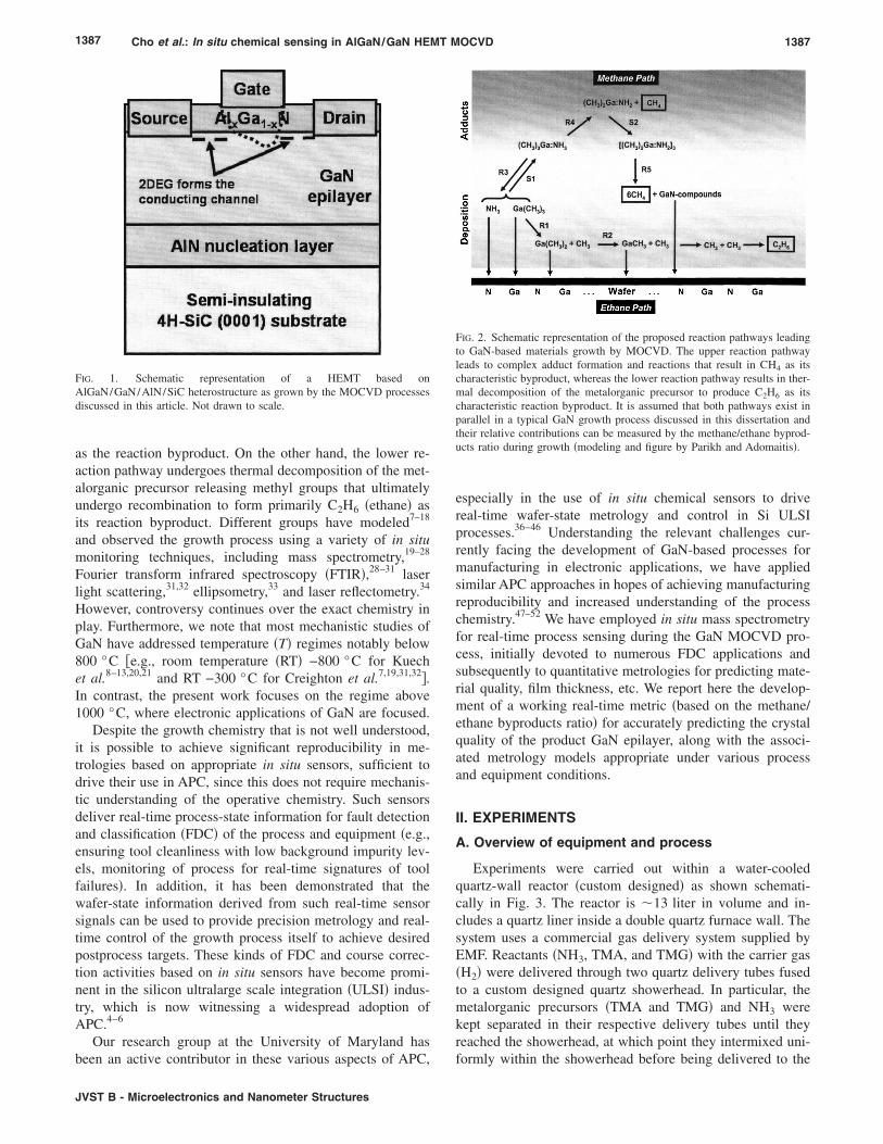
Although GaN metalorganic chemical vapor deposition�MOCVD� processes have been investigated in some depth,its intrinsic chemistry is still debated.7–34 Typically, MOCVDof GaN and AlGaN heteroepitaxial films �as shown in Fig. 1for example� are grown at high temperatures �e.g., up to1100 °C� using large concentrations of H2 �carrier� and NH3
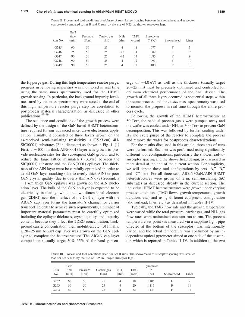
�N source�, and relatively small concentrations of metal�group III� precursors, trimethylgallium �TMG� or trimethy-laluminum �TMA�. The variety of active species and reactionpathways accessible at such elevated temperatures give riseto complex parasitic reactions in the gas phase as shown inFig. 2.35 GaN growth is characterized by two competing re-action pathways occurring in the gas phase. The upper reac-tion pathway leads to form complex adduct species whichfurther decompose to form a trimer specie before finally de-composing to form GaN on the hot wafer surface. This ad-
duct pathway releases several molecules of CH4 �methane�138623„4…/1386/12/$22.00 ©2005 American Vacuum Society
1387 Cho et al.: In situ chemical sensing in AlGaN/GaN HEMT MOCVD 1387
as the reaction byproduct. On the other hand, the lower re-action pathway undergoes thermal decomposition of the met-alorganic precursor releasing methyl groups that ultimatelyundergo recombination to form primarily C2H6 �ethane� asits reaction byproduct. Different groups have modeled7–18
and observed the growth process using a variety of in situmonitoring techniques, including mass spectrometry,19–28
Fourier transform infrared spectroscopy �FTIR�,28–31 laserlight scattering,31,32 ellipsometry,33 and laser reflectometry.34
However, controversy continues over the exact chemistry inplay. Furthermore, we note that most mechanistic studies ofGaN have addressed temperature �T� regimes notably below800 °C �e.g., room temperature �RT� −800 °C for Kuechet al.8–13,20,21 and RT −300 °C for Creighton et al.7,19,31,32�.In contrast, the present work focuses on the regime above1000 °C, where electronic applications of GaN are focused.
Despite the growth chemistry that is not well understood,it is possible to achieve significant reproducibility in me-trologies based on appropriate in situ sensors, sufficient todrive their use in APC, since this does not require mechanis-tic understanding of the operative chemistry. Such sensorsdeliver real-time process-state information for fault detectionand classification �FDC� of the process and equipment �e.g.,ensuring tool cleanliness with low background impurity lev-els, monitoring of process for real-time signatures of toolfailures�. In addition, it has been demonstrated that thewafer-state information derived from such real-time sensorsignals can be used to provide precision metrology and real-time control of the growth process itself to achieve desiredpostprocess targets. These kinds of FDC and course correc-tion activities based on in situ sensors have become promi-nent in the silicon ultralarge scale integration �ULSI� indus-try, which is now witnessing a widespread adoption ofAPC.4–6
Our research group at the University of Maryland has
FIG. 1. Schematic representation of a HEMT based onAlGaN/GaN/AlN/SiC heterostructure as grown by the MOCVD processesdiscussed in this article. Not drawn to scale.
been an active contributor in these various aspects of APC,
JVST B - Microelectronics and Nanometer Structures
especially in the use of in situ chemical sensors to drivereal-time wafer-state metrology and control in Si ULSIprocesses.36–46 Understanding the relevant challenges cur-rently facing the development of GaN-based processes formanufacturing in electronic applications, we have appliedsimilar APC approaches in hopes of achieving manufacturingreproducibility and increased understanding of the processchemistry.47–52 We have employed in situ mass spectrometryfor real-time process sensing during the GaN MOCVD pro-cess, initially devoted to numerous FDC applications andsubsequently to quantitative metrologies for predicting mate-rial quality, film thickness, etc. We report here the develop-ment of a working real-time metric �based on the methane/ethane byproducts ratio� for accurately predicting the crystalquality of the product GaN epilayer, along with the associ-ated metrology models appropriate under various processand equipment conditions.
II. EXPERIMENTS
A. Overview of equipment and process
Experiments were carried out within a water-cooledquartz-wall reactor �custom designed� as shown schemati-cally in Fig. 3. The reactor is �13 liter in volume and in-cludes a quartz liner inside a double quartz furnace wall. Thesystem uses a commercial gas delivery system supplied byEMF. Reactants �NH3, TMA, and TMG� with the carrier gas�H2� were delivered through two quartz delivery tubes fusedto a custom designed quartz showerhead. In particular, themetalorganic precursors �TMA and TMG� and NH3 werekept separated in their respective delivery tubes until theyreached the showerhead, at which point they intermixed uni-
FIG. 2. Schematic representation of the proposed reaction pathways leadingto GaN-based materials growth by MOCVD. The upper reaction pathwayleads to complex adduct formation and reactions that result in CH4 as itscharacteristic byproduct, whereas the lower reaction pathway results in ther-mal decomposition of the metalorganic precursor to produce C2H6 as itscharacteristic reaction byproduct. It is assumed that both pathways exist inparallel in a typical GaN growth process discussed in this dissertation andtheir relative contributions can be measured by the methane/ethane byprod-ucts ratio during growth �modeling and figure by Parikh and Adomaitis�.
formly within the showerhead before being delivered to the

1388 Cho et al.: In situ chemical sensing in AlGaN/GaN HEMT MOCVD 1388
wafer region below. Single-wafer substrate �2 in. diam semi-insulating SiC from Cree� was placed on the SiC-coatedgraphite susceptor. The susceptor was inductively heated at10 kHz to provide heating for the film growth to occur on thewafer. The residual process gases were continuously pumpedaway through the exhaust lines located at both ends of thereactor, connected to a common rotary vane pump.
B. HEMT heterostructure growth by MOCVD
The typical process sequence used to grow GaN-basedhigh electron mobility transistor �HEMT� heterostructures inour experiments is described in Table I. It began with30–60 min of pregrowth room temperature reactor purge.
FIG. 3. Schematic representation of the 200 amu in situ quadrupole mass spthe quartz wall reactor system for the GaN-based MOCVD processes discu
TABLE I. Typical MOCVD process sequence used tothe article.
Step No. Description Duration
1 RT reactorpurge
30–60 min
2 T ramp up 20 min3 High T reactor
purge5 min
4 AlN growth �15 min
5 GaN growth 60–90 min
7 AlGaN growth 1–3 min
8 Cooling with NH3 1 min
9 Cooling with NH3 12 min10 Cooling with H2 15 min11 Cycle purge 5 min 20 s
J. Vac. Sci. Technol. B, Vol. 23, No. 4, Jul/Aug 2005
During this period, the reactor �including the showerhead,liner, and susceptor� was purged with 25 slm of H2 at roomtemperature without intentional heating of the susceptor.Once the reactor has undergone sufficiently long purge toachieve acceptable low levels of background impurities�H2O, O2, etc.� as monitored by the mass spectrometry, heat-ing of the susceptor was initiated. During this step, tempera-ture was ramped at �1 °C/s until it reached the desired setpoint for growth �typically 1000–1200 °C as measured via asapphire light pipe directed at the bottom of the susceptor�.Once the temperature reached its final set point, it was main-tained for an additional 5 min to outgas background impuri-ties from both the susceptor and the liner in the presence of
eter gas sampling system �Inficon CPM™� attached to the downstream ofn this article.
the GaN-based HEMT heterostructure discussed in
ressure �Torr� Temperature Gases on
50 RT H2
50 Heating H2
50 At growth T H2
50 At growth T H2, NH3
TMA50 At growth T H2, NH3,
TMG50 At growth T H2, NH3,
TMA, TMGPump down
��45�Cooling H2, NH3
300 Cooling H2, NH3
300 Cooling H2
5↔450 RT H2
ectromssed i
grow
P
1389 Cho et al.: In situ chemical sensing in AlGaN/GaN HEMT MOCVD 1389
the H2 purge gas. During this high temperature reactor purge,progress in removing impurities was monitored in real timeusing the same mass spectrometry used for the HEMTgrowth sensing. In particular, the background impurity levelsmeasured by the mass spectrometry were noted at the end ofthis high temperature reactor purge step for correlation topostprocess material characterization, as discussed in otherpublications.47–49
The sequence and conditions of the growth process weredefined by the design of the GaN-based HEMT heterostruc-ture required for our advanced microwave electronics appli-cation. Usually, it consisted of three layers grown on theas-received semi-insulating �resistivity �1E5 � cm� 4H-SiC�0001� substrates �2 in. diameter� as shown in Fig. 1. �1�First, a �100 nm thick AlN�0001� layer was grown to pro-vide nucleation sites for the subsequent GaN growth and toreduce the large lattice mismatch ��3.3% � between theSiC�0001� substrate and the GaN�0001� epilayer. The thick-ness of the AlN layer must be carefully optimized in order toavoid GaN layer cracking �due to overly thick AlN� or poorGaN crystal quality �due to overly thin AlN�. �2� Second, a�1 �m thick GaN epilayer was grown on the AlN nucle-ation layer. The bulk of the GaN epilayer is expected to beelectrically insulating, while the two-dimensional electrongas �2DEG� near the interface of the GaN epilayer with theAlGaN cap layer forms the transistor’s channel for carriertransport. In order to achieve such requirements, a number ofimportant material parameters must be carefully optimizedincluding the epilayer thickness, crystal quality, and impuritycontent, because they affect the 2DEG concentration, back-ground carrier concentration, their mobilities, etc. �3� Finally,a 20–25 nm AlGaN cap layer was grown on the GaN epil-ayer to complete the heterostructure. The AlGaN cap layercomposition �usually target 30%–35% Al for band gap en-
TABLE II. Process and tool conditions used for set A ruwas created compared to set B and C runs by the us
Run No.
GaNtime�min�
Pressure�Torr�
Carrier gas�slm�
N�
G245 90 50 25G246 75 50 25G247 90 50 25G248 90 50 25G249 90 50 25
TABLE III. Process and tool conditions used for set Bthan for set A runs by the use of 0.25 in. longer susc
RunNo.
GaNtime�min�
Pressure�Torr�
Carrier gas�slm�
N�sl
G262 60 50 25 4G263 60 50 25 4G264 60 50 25 4
JVST B - Microelectronics and Nanometer Structures
ergy of �4.0 eV� as well as the thickness �usually target20–25 nm� must be precisely optimized and controlled foroptimum electrical performance of the final device. Thegrowth of all three layers occurred as sequential steps withinthe same process, and the in situ mass spectrometry was usedto monitor the progress in real time through the entire pro-cess cycle.
Following the growth of the HEMT heterostructure at50 Torr, the residual process gases were pumped away andthe wafer was cooled under NH3 at 300 Torr to prevent GaNdecomposition. This was followed by further cooling underH2 and cycle purge of the reactor to complete the processand remove the wafer for postprocess characterizations.
For the results discussed in this article, three sets of runswere performed. Each set was performed using significantlydifferent tool configurations, particularly the showerhead-to-susceptor spacing and the showerhead design, as discussed inmore detail at the end of the current section. For simplicity,we will denote these tool configurations by sets “A,” “B,”and “C” here. For all three sets, AlGaN/GaN/AlN HEMTheterostructures were grown on 2 in. semi-insulating SiCsubstrates as discussed already in the current section. Theindividual HEMT heterostructures were grown under varyingprocess conditions �TMG flows, growth temperature, growthduration, etc.� and using different equipment configuration�showerhead, liner, etc.� as described in Tables II–IV.
Typically, the TMG flow rate and the growth temperaturewere varied while the total pressure, carrier gas, and NH3 gasflow rates were maintained constant run-to-run. The processtemperature set point �as measured via a sapphire light pipedirected at the bottom of the susceptor� was intentionallyvaried, and the actual temperature was confirmed by an in-dependent optical pyrometer aimed at one side of the suscep-tor, which is reported in Tables II–IV. In addition to the two
arger spacing between the showerhead and susceptor.25 in. shorter susceptor legs.
TMG�sccm�
PyrometerT �°C� Showerhead Liner
11 1077 F 314 1082 F 914 1085 F 912 1093 F 1012 1100 F 10
s. The showerhead to susceptor spacing was smallerlegs.
TMG�sccm�
PyrometerT
�°C� Showerhead Liner
18 1106 F 920 1115 F 1122 1130 F 11
ns. Le of 0
H3
slm�
43.84.244
runeptor
H3
m�
1390 Cho et al.: In situ chemical sensing in AlGaN/GaN HEMT MOCVD 1390
types of direct temperature measurements, other indirectmeans to infer the actual process temperature were also em-ployed, including measurement of the cooling water tem-perature exiting the reactor and the utilized rf power output.
The showerheads were made of quartz and custom-designed by one of our co-authors �R. Adomaitis� through aphysically based model describing heat transfer and gastransport through the showerhead.53 For example, shower-heads “F” �used for set A and B runs� and “G” �used for setC runs� differed markedly in their hole pattern, size, anddistribution. Both the showerhead and the innermost linerwere removed from the reactor after each run. Showerheadswere cleaned in ultrasonic KOH solution bath run-to-run,while the liners were used for �3 runs without cleaning. Onaverage, a showerhead could be used for �10 runs beforebeing replaced due to the effect of the showerhead surfaceroughening on film growth uniformity. Finally, theshowerhead-to-susceptor spacing was intentionally varied bythe use of 0.25 in. longer susceptor legs for sets B and Ccompared to set A.
C. Real-time in situ process sensingby mass spectrometry
The mass spectrometry sampling system used is shownschematically in Fig. 3. The process and residual gases weresampled directly from the reactor downstream via a1/16 in. o.d.�0.010 in. i.d.�20 cm long stainless steelcapillary, which resulted in a pressure drop from the processpressure of 50 Torr down to �1 Torr behind the capillary.Most of this gas was then pumped away by a bypass differ-ential pumping to the foreline of the diaphragm pump �back-ing pump for the mass spectrometer’s turbomolecular pump�,leaving only a small fraction of the gas to enter a 20 �m i.d.orifice into the closed ion source region of the mass spec�Inficon model CPM™, 200 amu quadrupole mass spectrom-eter�.
By using an appropriately sized capillary-orifice combina-tion for the gas conductance network, the sampled gas pres-sure was reduced from the viscous flow regime �50 Torr� tothe molecular flow regime ��1 Torr�. The bypass differen-tial pumping technique enabled us to actively withdrawgases from the process through the sampling system. Both of
TABLE IV. Process and tool conditions used for set Cthan for set A runs by the use of 0.25 in. longer suscepattern were used compared to set A and B runs.
RunNo.
GaNtime�min�
Pressure�Torr�
Carrier gas�slm�
N�sl
G379 90 50 15 3G380 90 50 15 3G382 95 50 15 3G386 90 50 15 3
these sampling techniques, as well as the location of the
J. Vac. Sci. Technol. B, Vol. 23, No. 4, Jul/Aug 2005
sampling capillary �i.e., within the main gas flow down-stream to the growth reaction�, were critical in achievingadequate response time in process sensing.
The W filament current in the closed ion source was keptat 200 �A, while the electron energy was maintained at40 eV. This provided adequate sensitivity and minimumparasitic reactions within the closed ion source region. Elec-tron multiplier detection was used at an acceleration voltagesof 1000 V �for sets A and B� and 835 V �for set C after theelectron multiplier unit was replaced� to enhance and main-tain the signal-to-noise ratio run-to-run.
D. Postprocess material characterizations
The samples grown on SiC substrates as described in thepreceding sections were examined using a number of post-process characterization techniques, including x-ray diffrac-tion �XRD�, x-ray reflectance �XRR�, and photolumines-cence �PL�. In particular, the XRD was performed using aBede D1™ system equipped with microsource capability forhigher spatial resolution. Rocking curves were obtained at 81points on an equally spaced rectangular grid over the 2 in.wafer. Full-width at half-maximum �FWHM� height of theindividual rocking curves were obtained and averaged toprovide a measure of the average crystal quality of the GaNepilayer. For set A runs, FWHMs were measured for both theon-axis �002� symmetric and off-axis �102� glancing exit re-flections. The on-axis reflection �most commonly reported�alone is considered to be insufficient as a metric for GaNcrystal quality because it is not affected by edge dislocations�i.e., the material can have large density of edge dislocationsand still produce a narrow �002� peak�. However, it wasfound over the course of many runs that the presence of thetwo types of defects �edge and screw dislocations� were ingeneral correlated �i.e., found together�, and the off-axis�102� reflection therefore did not provide any additional in-formation to that from the on-axis �002� reflection. Also, inan effort to improve our throughput, the number of pointsanalyzed across the wafer was reduced to nine for set C runs.
III. RESULTS
A. Real-time in situ metrology development
. The showerhead to susceptor spacing was smalleregs. Also, showerheads with markedly different hole
TMG�sccm�
PyrometerT
�°C� Showerhead Liner
15 1111 G 315 1102 G 320 1111 G 1220 1113 G 18
runsptor l
H3
m�
In situ mass spectrometry sensing of the 50 Torr MOCVD

1391 Cho et al.: In situ chemical sensing in AlGaN/GaN HEMT MOCVD 1391
growth process as described above provided dynamic, real-time gas phase chemical signals as a function of the processcycle. Figures 4 and 5 show characteristic ion current signalsfrom H2 �carrier gas�, NH3 �column V precursor�, N2 �frag-mentation product from NH3�, H2O �background impurity�,CH4 �reaction byproduct�, C2H6 �reaction byproduct�, C�background impurity�, and O2 �background impurity�. Par-tial pressures for these species, reflected in the ion currents,exhibit strong time dependence throughout the entire processcycle, including the initial and final stages of the AlN, GaN,and AlGaN growth steps. This is primarily a consequence ofthe reactor residence time, which determines the rate atwhich reaction byproduct generation and reactant depletionattain steady state whenever there is a change in processchemistry �e.g., going from GaN growth to AlGaN ternaryalloy growth�. Virtually no column III precursors �TMA andTMG� were detectable in their original chemical form at thedownstream location. This is primarily attributed to the closeto complete decomposition and utilization at the extremelyhigh growth temperature near the wafer and showerhead re-gions. Note also that for the reaction byproducts methaneand ethane, mass peaks at 13 and 26 amu were used insteadof 16 and 30 amu as one might expect �based on NISTdatabase54�. These values were chosen from components inthe fragmentation patterns of the parent species to minimizeambiguity where mass fragments from multiple sourcesoverlap. Specifically, this was an attempt to avoid large over-lap in spectrum for the species present in the system includ-ing NH3 �fragmentation pattern at 17, 16, 15, and 14 amu�and N2 �fragmentation pattern at 28 and 14 amu; and para-sitic ion-molecule reactions to produce Nx-Hy species at 15,16, 29, and 30 amu�. Small overlaps ��8% � may have ex-isted between methane and ethane signals knowing that ad-ditional methane can be formed inside mass spectrometer ion
FIG. 4. In situ gas phase chemical signals from mass spectrometry, indica-tive of the dynamic gas composition downstream of the reactor as a functionof process steps. The mass spectrometry current signals were acquired inreal time through the entire HEMT growth process. Shown here is an ex-ample taken from run G262, for which the equipment configurations andprocess conditions are described in Table III.
source as a fragment of the original ethane from the
JVST B - Microelectronics and Nanometer Structures
MOCVD reaction. However, with the fixed operating condi-tion for the mass spectrometry, the minute overlap would beconsistent run-to-run and therefore negligible for the purposeof our analysis described below.
Because methane and ethane are clearly the byproducts ofthe growth reaction of our interest, it is expected that theycontain the wafer-state information indicative of depositionon the wafer, as well as the process-state information nor-mally expected. It has already been clearly demonstrated inthe past that these kinds of in situ sensor-based signals doindeed correlate to the wafer state in real time, in some caseswith high quantitative precision that allows precisionmetrology46 and subsequent control43 of the wafer state �e.g.,film thickness deposited�. Moreover, in this case, assumingthat each of the two byproducts come from different reactionpathways to grow the GaN-based material on the wafer �seeFig. 2�, the methane/ethane ratio can be thought of as a mea-sure of the relative contribution of each pathway for anygiven growth process. With this in mind, the methane/ethaneratio can be directly monitored in real time as shown in Fig.5. Averaging the values obtained through the entire GaNgrowth period provides the average methane/ethane ratiometric of our interest:
�S�CH4�dt
�S�C2H6�dt. �1�
Next, we show how this sensor-based metric can be used topredict the product crystal quality in real time and the corre-sponding metrology results we have obtained in our three
FIG. 5. In situ gas phase chemical signals from mass spectrometry, indica-tive of the dynamic gas composition downstream of the reactor as a functionof process steps. Shown here are the reaction byproducts methane �at13 amu� and ethane �at 26 amu� through the AlN, GaN, and AlGaN layergrowth steps along with the corresponding methane/ethane ratio metric de-rived in real time. This example is taken from run G262, the same run as inFig. 4.
sets of GaN growth runs.
1392 Cho et al.: In situ chemical sensing in AlGaN/GaN HEMT MOCVD 1392
B. Real-time prediction of GaN crystal qualityand metrology
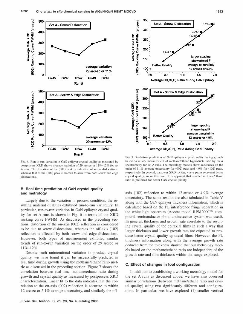
Largely due to the variation in process condition, the re-sulting material qualities exhibited run-to-run variability. Inparticular, run-to-run variation in GaN epilayer crystal qual-ity for set A runs is shown in Fig. 6 in terms of the XRDrocking curve FWHM. As discussed in the preceding sec-tions, distortion of the on-axis �002� reflection is consideredto be due to screw dislocations, whereas the off-axis �102�reflection is affected by both screw and edge dislocations.However, both types of measurement exhibited similartrends of run-to-run variation on the order of 29 arcsec or11%–12%.
Despite such unintentional variation in product crystalquality, we have found it can be successfully predicted inreal time during growth using the methane/ethane ratio met-ric as discussed in the preceding section. Figure 7 shows thecorrelation between real-time methane/ethane ratio duringgrowth and crystal quality as measured by postprocess XRDcharacterization. Linear fit to the data indicates that the cor-relation to the on-axis �002� reflection is accurate to within
FIG. 6. Run-to-run variation in GaN epilayer crystal quality as measured bypostprocess XRD shows average variation of 29 arcsec or 11%–12% for setA runs. The distortion of the �002� peak is indicative of screw dislocations,whereas that of the �102� peak is known to arise from both screw and edgedislocations.
12 arcsec or 5.1% average uncertainty, and similarly the off-
J. Vac. Sci. Technol. B, Vol. 23, No. 4, Jul/Aug 2005
axis �102� reflection to within 12 arcsec or 4.9% averageuncertainty. The same results are also tabulated in Table Valong with the GaN epilayer thickness information, which iscalculated based on the PL interference fringe separation inthe white light spectrum �Accent model RPM2000™ com-pound semiconductor photoluminescence system was used�.In general, thickness and growth rate correlate to the result-ing crystal quality of the epitaxial films in such a way thatlarger thickness and lower growth rate are expected to pro-duce better crystal quality epitaxial films. However, the PLthickness information along with the average growth ratededuced from the thickness showed that our metrology mod-els based on the methane/ethane ratio are independent of thegrowth rate and film thickness within the range explored.
C. Effect of changes in tool configuration
In addition to establishing a working metrology model forthe set A runs as discussed above, we have also observedsimilar correlations �between methane/ethane ratio and crys-tal quality� using two significantly different tool configura-
FIG. 7. Real-time prediction of GaN epilayer crystal quality during growthbased on in situ measurement of methane/ethane byproducts ratio by massspectrometry for set A runs. The metrology models show accuracies on theorder of 5.1% average uncertainty for �002� peak and 4.9% for �102� peak,respectively. In general, narrower XRD rocking curve peaks represent bettercrystal quality, so in this case, it is apparent that smaller methane/ethaneratio is preferred for better GaN crystal quality.
tions. In particular, we have explored �1� smaller vertical

1393 Cho et al.: In situ chemical sensing in AlGaN/GaN HEMT MOCVD 1393
spacing between the showerhead and susceptor in sets B andC �Fig. 8, Table VI� and �2� significantly different shower-head design in terms of its hole pattern, size, and distributionin set C �Fig. 9, Table VII�.
Overall results indicate that small methane/ethane byprod-uct ratios identify better GaN epilayer crystal quality, withthe corresponding metrology accurate to within 2%–5% av-erage uncertainty, depending on the tool configuration andthe associated model for the different set of runs. This isconfirmed by the correlation between the real-time methane/ethane ratio measured by in situ chemical sensing of thereaction byproducts and the postprocess GaN crystal qualitymeasured by XRD for changes in process conditions at afixed tool configuration. In turn, significant changes in toolconfiguration �i.e., the showerhead design and the spacingbetween showerhead and susceptor� necessitated a change inthe model, but for each tool configuration a model gave astrong correlation between mass spectrometry metrology andcrystal quality.
FIG. 8. Real-time prediction of GaN epilayer crystal quality during growthbased on in situ measurement of methane/ethane byproducts ratio by massspectrometry for set B runs. The metrology model shows accuracy on theorder of 2.0% average uncertanity for the �002� peak. In general, narrowerXRD rocking curve peaks represent better crystal quality, so in this case, itis apparent that smaller methane/ethane ratio is preferred for better crystalquality GaN. Identical showerhead design, but a smaller showerhead to
TABLE V. Postprocess GaN epilayer characterization for set A runs. GaN epbe deduced. XRD rocking curve FWHM provided a measure of epilayer cryscrew dislocations, whereas the off-axis �102� reflection is considered to be ain-situ mass spectrometry serves as our real-time crystal quality prediction
RunNo.
Thicknessby PL��m�
Average growthrate ��m/h�
G245 0.695 0.46G246 1.354 1.08G247 1.553 1.04G248 1.305 0.87G249 0.650 0.43
susceptor spacing �0.25 in. less�, was used compared to set A runs.
JVST B - Microelectronics and Nanometer Structures
IV. DISCUSSION
A. Elements that determine metrology/control model
The metrology models developed above, based on corre-lation between real-time mass spectrometry measurements ofmethane/ethane ratios and postprocess GaN crystal qualitycharacterization by XRD, display substantial validity �a few%� in the presence of modest intentional changes made inrun-to-run process condition within each set as seen in TablesII–IV. There also existed numerous nonintentional factorswithin each individual set in terms of the growth conditions,which ultimately contributed to the run-to-run material qual-ity variation but was still well described by the model.
For example, as the showerhead aged run-to-run, its sur-face roughened �i.e., area increased� due to bonding of ma-terials during process and their removal during postprocessKOH cleaning; this affected the depletion of the precursorwithin the showerhead and therefore the film growth unifor-mity on the wafer. The use of different liners brought aboutslight variation in the showerhead-to-susceptor spacing be-cause the showerhead was designed to rest on the horizontal
FIG. 9. Real-time prediction of GaN epilayer crystal quality during growthbased on in situ measurement of methane/ethane byproducts ratio by massspectrometry for set C runs. The metrology model shows accuracy on theorder of 3.5% average uncertainty for the �002� peak. In general, narrowerXRD rocking curve peaks represent better crystal quality, so in this case, itis apparent that smaller methane/ethane ratio is preferred for better crystalquality GaN. A completely different showerhead design, but an identical
thickness was measured by PL, from which the average growth rate couldquality. Distortion of the on-axis �002� reflection is considered to be due tod by both screw and edge dislocations. Methane/ethane ratio obtained from
c.
ane/ethaneratio
XRD FWHM at�002�
XRD FWHM at�102�
1.51 269 2441.33 223 2270.71 187 1691.58 290 2921.92 330 315
ilayerstalffectemetri
Meth
showerhead to susceptor spacing, was used compared to set B runs.

1394 Cho et al.: In situ chemical sensing in AlGaN/GaN HEMT MOCVD 1394
crossbar built into the liner itself, whose position uninten-tionally varied to within the glass fabrication error of�0.125 in. This would have affected the temperature andchemistry within the showerhead positioned directly abovethe hot susceptor. In fact, variability observed in the run-to-run sensing data motivated a reactor design modification toeliminate the liner as a source of such variability for futureruns. These types of influences on the gas phase chemistryduring the process are expected to manifest in terms of thefinal material quality such as the crystal quality. Finally, con-ditions of the underlying AlN nucleation layer and SiC sub-strate were inconsistent run-to-run, which would have influ-enced the GaN epilayer grown over them. This has beenproven through our routine XRD wafer mapping, where theoriginal defects within the SiC substrate could indeed trans-late to undesirable defects within the AlN and GaN layersgrown over them, unless steps were taken during the AlNlayer growth to minimize their effect.51
Despite all of these intentional and nonintentional sourcesof variability that lead to run-to-run variations in the processenvironment and resulting material quality, results show thata single model developed using one tool configuration pro-vides quantitative predictability of crystal quality over a rea-sonable range of process conditions. However, the modelsindicate strong dependence on the tool configuration param-eters such as the showerhead-to-susceptor spacing and theshowerhead design. These points are illustrated clearly inFig. 10. The model relating mass spectrometry predictors ofcrystal quality and actual XRD measures of crystal qualitychanges significantly with changes in tool configuration.However, once the tool configuration is fixed, the associatedmodel transforms the mass spectrometry measurement intoan effective predictor of material quality �to a few % preci-sion�.
B. Prognosis for applications
Even though the XRD rocking curve data are only sup-posed to reflect a qualitative or semiquantitative measure of amaterial’s crystal quality, such a correlation as seen here be-tween real-time wafer-state metric based on sensors andpostprocess product quality can be extremely useful from theviewpoints of both development and manufacturing.
The methane/ethane ratio offers an extremely useful met-
TABLE VI. Postprocess GaN epilayer characterization for set B runs. GaNepilayer thickness was measured by PL, from which the average growth ratecould be deduced. XRD rocking curve FWHM provided a measure of epil-ayer crystal quality. Methane/ethane ratio obtained from in-situ mass spec-trometry serves as our real-time crystal quality prediction metric.
RunNo.
Thickness byPL ��m�
Average growthrate ��m/h�
Methane/ethaneratio
XRD FWHM at�002�
G262 1.197 1.20 2.32 199G263 1.449 1.45 2.44 248G264 1.173 1.17 2.53 266
ric that can be quickly utilized to identify process conditions
J. Vac. Sci. Technol. B, Vol. 23, No. 4, Jul/Aug 2005
that optimize product crystal quality. With GaN technologiesstill in development, this is extremely useful. For instance, asingle design of experiment �DOE�, containing multipleshort period ��30 s� GaN growth steps within to explore awide range of process conditions �in terms of temperature,pressure, flow rates, gas composition, etc.�, may be per-formed on a semi-insulating SiC with a usual AlN nucleationlayer. The average methane/ethane ratio resulting from eachindividual GaN growth step can be monitored and recordedin real time. Knowing that lower methane/ethane ratio willhave a greater chance of producing better GaN crystal qual-ity, an optimal window of process condition can be selectedand employed in subsequent real HEMT heterostructuregrowth runs. This offers a systematic methodology toimprove/tune GaN-based processes with drastically reducedturnaround time and cost.
Furthermore, since the metric is based on real-time in situmetrology, it can be exploited for real-time control of theMOCVD growth process in the context of APC. In one sce-
TABLE VII. Postprocess GaN epilayer characterization for set C runs. GaNepilayer thickness was measured by PL, from which the average growth ratecould be deduced. XRD rocking curve FWHM provided a measure of epil-ayer crystal quality. Methane/ethane ratio obtained from in-situ mass spec-trometry serves as our real-time crystal quality prediction metric.
RunNo.
Thickness byPL ��m�
Average growthrate ��m/h�
Methane/ethaneratio
XRD FWHM at�002�
G379 0.860 0.57 2.01 189G380 0.805 0.54 2.16 296G382 0.925 0.58 2.17 273G386 1.083 0.72 2.12 242
FIG. 10. Crystal quality prediction models for three different tool configu-rations in terms of the showerhead to susceptor spacing �larger versussmaller spacing� and the showerhead design �F versus G�. It is apparent thatthe critical variables giving rise to a set of different metrology models arethe tool configuration parameters �the showerhead-to-susceptor spacing andthe specific showerhead design�, not the small changes made, within eachset, in temperature, gas flow rates, composition, liners, etc. Therefore, weconclude that once we define the tool configurations/geometries for ourprocesses, we are practically defining the elements that determine the
metrology/control model.
1395 Cho et al.: In situ chemical sensing in AlGaN/GaN HEMT MOCVD 1395
nario, the mass spectrometry signature can be employed forfault detection, identifying in real time wafers for which ma-terial quality may be degraded and triggering corrective ac-tions ranging from more in-depth characterization to debug-ging and repair of equipment. Such FDC approaches havealready been widely adopted in the Si ULSI industry as dis-cussed in Sec. I.
In another scenario, the real-time mass spectrometry pre-dictors of material quality may be employed for course cor-rection. If an appropriate process parameter, or a set of pa-rameters, can be identified which can improve materialquality as reflected in the methane/ethane ratio, then drift inthis ratio could be compensated in real time. ImplementingDOEs as discussed already in the current section may aid inrevealing the most appropriate and effective process param-eters for this purpose. Such real-time course correction couldprovide significant advantage in terms of achieving repro-ducibility and yield by minimizing the number of scrap wa-fers and wasted runs due to unacceptable GaN crystal qual-ity. Consequent cost reduction could be large, consideringthe irreproducibility and drift levels in the current GaN tech-nology as well as the high per wafer materials cost in GaN-based manufacturing.
C. Implications in terms of intrinsic chemistry
One of the advantages of the foregoing application ofreal-time chemical sensing and metrology for manufacturingprocess control is that it does not require a complete under-standing of the intrinsic chemistry, and can be exploitedreadily. Therefore, the current debate over the relevant reac-tion pathway and the parasitic reactions does not seem to bea major bottleneck in GaN-based technology and manufac-turing for now. However, in the long run, better understand-ing of fundamental mechanisms will no doubt help in termsof being able to optimize process conditions, and materialsand device performance.
As discussed in Sec. I, current understanding of the GaN-based MOCVD process suggests there are two competingreaction pathways, i.e., the adduct formation route and thethermal decomposition route, both occurring in the gasphase. Prior investigations have focused on significantlylower temperature regimes �RT −800 °C� than those treatedhere for electronic applications ��1000 °C�. Modeling workperformed within our research group35 indicates that the op-erative process chemistry changes significantly with varia-tions in reactor operating parameters, particularly in terms ofthe relative contributions of the two different reaction path-ways. For example, increase in chamber pressure enhancesthe adduct formation route and ultimately increases theamount of methane because this reaction is given by a bimo-lecular collision rate expression. Additionally, as the tem-perature is raised, both reaction routes may occur in parallel.For additional details, refer to Ref. 35.
Currently, a debate exists over which reaction pathway isresponsible for GaN growth. One side believes that GaNgrowth is dominated by the upper route mainly through the
8–10,16
formation of the cyclic trimer species. The other side ofJVST B - Microelectronics and Nanometer Structures
the argument believes that GaN growth is dominated by thelower route through pyrolysis of the metalorganicprecursor.14,25 Essentially, both reaction pathways are pos-sible, and the selectivity between the two reaction rate pa-rameters are significantly influenced by the choice of reactoroperating conditions, residence time in heated zones, degreeof precursor mixing as determined by the design of the gasdelivery system, reactor geometry, and the choice of reactionrate parameters.35
The methane/ethane ratio metric can be monitored, sinceethane is assumed to be produced as a byproduct of the ther-mal decomposition route and not the adduct route. We planfurther exploratory investigations to elucidate these issuesrelated to the intrinsic process chemistry. It is also acknowl-edged that our studies are rather limited to specific process/tool conditions geared towards electronic applications ofGaN �i.e., high T�1000 °C, semi-insulating SiC substrate�.In any case, all of our results to date indicate that the directdecomposition of the metalorganic precursor leads to bettercrystal quality than does the adduct pathway. However, it isacknowledged that our studies are focused on specificprocess/tool conditions geared towards electronic applica-tions of GaN �e.g., �1000 °C, semi-insulating SiC sub-strate�.
D. Other material quality metrics of importance
In developing real-time, in situ methods for sensing, me-trology, and control as reported here, we have focused oncrystalline perfection characterized by XRD as the measureof material quality. However, this is certainly not the onlymeasure of a material’s quality: other relevant and importantmeasures include PL, XRR, sheet resistance, Hall effectmeasurement, secondary ion mass spectrometry, etc. Wehave routinely examined our HEMT heterostructure films us-ing these postprocess techniques. In particular, the samex-ray machine �Bede D1™ system� was also used to measurethe thickness of the AlGaN cap layer ��20 nm�, where theseparation of interference fringes in the XRR mode gaveinformation on the thin layer’s thickness. Usually prior to allother types of characterization, PL was performed to obtainvarious measures of material quality, such as the band-edgeand deep-level intensities, thickness of the GaN epilayer��1 �m�, and the composition of the AlGaN cap layer. Inaddition, due to the nature of our application in high fre-quency and power electronics, electrical measurements suchas sheet resistance and Hall effect measurement for carriermobility are also important.
Optimization of all of these postprocess material qualitymetrics is important as well. Based on our results to date, weforesee analogous applications of real-time, in situ sensingfor metrology and APC tied to these material performancemetrics. For example, mass spectrometry may be useful forAlGaN cap layer thickness as a real-time course correctionapplication,50 while the correlation of mass spectrometry sig-nals to band-edge and/or deep-level PL may provide anotherapproach to FDC.49 Results along these lines will be dis-
cussed in separate publications.
1396 Cho et al.: In situ chemical sensing in AlGaN/GaN HEMT MOCVD 1396
V. CONCLUSIONS
In situ mass spectrometry sensing was implemented in50 Torr AlGaN/GaN/AlN/SiC HEMT heterostructuregrowth processes in order to enhance and control processreproducibility, and to achieve better understanding of theintrinsic chemistry involved. Dynamic chemical sensingthrough the process cycle, carried out downstream from thewafer, revealed generation of methane and ethane reactionbyproducts in real time, in addition to other residual gasspecies present in the process. Using the methane/ethane ra-tio, GaN epilayer crystal quality was shown to be predictablein real time during growth with quantitative precision of 2%–5%. This was verified by postprocess x-ray diffraction usingthe full-width at half-maximum height of GaN on-axis �002�and off-axis �102� rocking curve peaks as a measure of crys-tal quality. The same correlation was shown using three dif-ferent tool configurations with combinations of differentshowerhead designs and varied spacing between showerheadand susceptor.
The correlation shown here between the real-time wafer-state metric based on sensors and postprocess product qualityrepresents a significant advantage for GaN technology devel-opment in that it can be utilized in design of experiments toquickly identify the optimal range of process conditions forbest product quality. This offers a systematic methodology toimprove/tune GaN-based manufacturing processes with dras-tically reduced turn-around time and cost. The results alsopromise benefit to manufacturing process control in thegrowth of GaN-based heterostructures, both in terms of faultdetection and potential course correction as well, opening thedoor to the efficiencies and cost benefits of advanced processcontrol.
These results have further implications in terms of theintrinsic chemistry in that the two byproducts, methane andethane, are known to be associated with the two differentreaction pathways leading to GaN growth �i.e., gas phaseadduct formation route and gas phase thermal decompositionof precursor, respectively�. The fact that smaller methane/ethane ratio during process consistently yields better crystalquality GaN film suggests that the reaction pathway involv-ing direct thermal decomposition of the metalorganic precur-sor produces higher quality GaN material than does the ad-duct pathway.
In summary, this work shows significant benefit fromin situ mass spectrometry as a real-time process and waferstate sensor. Its ability to identify signatures of wafer statechanges correlated with material quality opens the door toexpedited development, manufacturing process control, andenhanced understanding of fundamental mechanisms.
ACKNOWLEDGMENTS
The authors are grateful for a close research partnershipwith, and financial support from, the Northrop GrummanCorporation. They also appreciate continuing interaction andtechnical support from Inficon, Inc., particularly R. Ellefson
and L. Frees. Inficon is a supplier of mass spectrometricJ. Vac. Sci. Technol. B, Vol. 23, No. 4, Jul/Aug 2005
sensors for process control applications in semiconductormanufacturing processes.
1L. F. Eastman and U. K. Mishra, IEEE Spectrum 5, 28 �2002�.2U. K. Mishra, P. Parikh, and Y. Wu, Proc. IEEE 90, 1022 �2002�.3R. J. Trew, Proc. IEEE 90, 1032 �2002�.4T. Sonderman, M. Miller, and C. Bode, Future Fab International 12, 119�2002�.
5S. W. Butler, J. Vac. Sci. Technol. B 13, 1917 �1995�.6G. G. Barna, B. V. Eck, and J. W. Hosch, Handbook of Silicon Semicon-ductor Metrology �Marcel Dekker, Inc., Austin, TX, 2001�, pp. 601–678.
7J. R. Creighton, J. Electron. Mater. 31, 1337 �2002�.8J. Sun, J. M. Redwing, and T. F. Kuech, J. Electron. Mater. 29, 2 �2000�.9J. Sun, J. M. Redwing, and T. F. Kuech, Phys. Status Solidi A 176, 693�1999�.
10S. A. Safvi, J. M. Redwing, M. A. Tischler, and T. F. Kuech, J. Electro-chem. Soc. 144, 1789 �1997�.
11D. D. Koleske, A. E. Wickenden, R. L. Henry, M. E. Twigg, J. C. Cul-bertson, and R. J. Gorman, MRS Internet J. Nitride Semicond. Res. 4S1,G3.70 �1999�.
12D. D. Koleske, A. E. Wickenden, R. L. Henry, M. E. Twigg, J. C. Cul-bertson, and R. J. Gorman, Appl. Phys. Lett. 73, 2018 �1998�.
13D. D. Koleske, A. E. Wickenden, R. L. Henry, W. J. DeSisto, and R. J.Gorman, J. Appl. Phys. 84, 1998 �1998�.
14R. P. Pawlowski, C. Theodoropoulos, A. G. Salinger, T. J. Mountziaris, H.K. Moffat, J. N. Shadid, and E. J. Thrush, J. Cryst. Growth 221, 622�2000�.
15A. Tachibana, O. Makino, S. Tanimura, H. Tokunaga, N. Akutsu, and K.Matsumoto, Phys. Status Solidi A 176, 699 �1999�.
16T. G. Mihopoulos, V. Gupta, and K. F. Jensen, J. Cryst. Growth 195, 733�1998�.
17C. H. Chen, H. Liu, D. Steigerwald, W. Imler, C. P. Kuo, M. G. Craford,M. Ludowise, S. Lester, and J. Amano, J. Electron. Mater. 25, 1004�1996�.
18Y. S. Hiraoka and M. Mashita, J. Cryst. Growth 136, 94 �1994�.19M. E. Bartram and J. R. Creighton, MRS Internet J. Nitride Semicond.
Res. 4S1, G3.68 �1999�.20A. Thon and T. F. Kuech, Appl. Phys. Lett. 69, 55 �1996�.21S. A. Safvi, A. Thon, J. M. Redwing, M. E. Tischler, and T. F. Kuech, in
Proceedings of the Thirteenth International Conference on Chemical Va-por Deposition, edited by T. M. Besmann, M. D. Allendorf, McD. Rob-inson, and R. K. Ulrich �Electrochemical Society, Pennington, NJ, 1996�,pp. 119–124.
22U. Bergmann, V. Reimer, and B. Atakan, Phys. Chem. Chem. Phys. 1,5593 �1999�.
23U. Bergmann, V. Reimer, and B. Atakan, Phys. Status Solidi A 176, 719�1999�.
24T. Li, R. P. Campion, C. T. Foxon, S. A. Rushworth, and L. M. Smith, J.Cryst. Growth 251, 499 �2003�.
25D. Sengupta, J. Phys. Chem. B 107, 291 �2003�.26J. Schafer, A. Simons, J. Wolfrum, and R. A. Fischer, Chem. Phys. Lett.
319, 477 �2000�.27C. A. Larsen, N. I. Buchan, S. H. Li, and G. B. Stringfellow, J. Cryst.
Growth 102, 103 �1990�.28M. J. Almond, M. G. B. Drew, C. E. Jenkins, and D. A. Rice, J. Chem.
Soc. Dalton Trans. 1992, 5 �1992�.29M. J. Almond, C. E. Jenkins, and D. A. Rice, J. Organomet. Chem. 439,
251 �1992�.30S. H. Kim, H. S. Kim, J. S. Hwang, J. G. Choi, and P. J. Chong, Chem.
Mater. 6, 278 �1994�.31J. R. Creighton, G. T. Wang, W. G. Breiland, and M. E. Coltrin, J. Cryst.
Growth 261, 204 �2004�.32J. R. Creighton, W. G. Breiland, M. E. Coltrin, and R. P. Pawlowski,
Appl. Phys. Lett. 81, 2626 �2002�.33M. Losurdo, P. Capezzuto, and G. Bruno, Phys. Status Solidi A 176, 733
�1999�.34A. Rebey, T. Boufaden, and B. E. Jani, J. Cryst. Growth 203, 12 �1999�.35R. P. Parikh and R. A. Adomaitis, J. Cryst. Growth �submitted�.36L. L. Tedder, G. W. Rubloff, I. Shareef, M. Anderle, D.-H. Kim, and G.
N. Parsons, J. Vac. Sci. Technol. B 13, 1924 �1995�.37L. L. Tedder, G. W. Rubloff, B. F. Cohaghan, and G. N. Parsons, J. Vac.
Sci. Technol. A 14, 267 �1996�.
1397 Cho et al.: In situ chemical sensing in AlGaN/GaN HEMT MOCVD 1397
38A. I. Chowdhury, W. W. Read, G. W. Rubloff, L. L. Tedder, and G. N.Parsons, J. Vac. Sci. Technol. B 15, 127 �1997�.
39G. Lu, L. L. Tedder, and G. W. Rubloff, J. Vac. Sci. Technol. B 17, 1417�1999�.
40T. Gougousi, Y. Xu, J. N. Kidder, Jr., G. W. Rubloff, and C. R. Tilford, J.Vac. Sci. Technol. B 18, 1352 �2000�.
41L. Henn-Lecordier, J. N. Kidder, Jr., G. W. Rubloff, C. A. Gogol, and A.Wajid, J. Vac. Sci. Technol. A 19, 621 �2001�.
42R. Sreenivasan, T. Gougousi, Y. Xu, J. Kidder, Jr., E. Zafiriou, and G. W.Rubloff, J. Vac. Sci. Technol. B 19, 1931 �2001�.
43Y. Xu, T. Gougousi, L. Henn-Lecordier, Y. Liu, S. Cho, and G. W.Rubloff, J. Vac. Sci. Technol. B 20, 2351 �2002�.
44L. Henn-Lecordier, J. N. Kidder, Jr., G. W. Rubloff, C. A. Gogol, and A.Wajid, J. Vac. Sci. Technol. B 21, 1055 �2003�.
45S. Cho, L. Henn-Lecordier, A. Singhal, Y. Xu, Y. Liu, J. N. Kidder, Jr.,and G. W. Rubloff, in AEC/APC Symposium XV, edited by InternationalSematech �International Sematech, Austin, TX, 2003�.
46S. Cho, L. Henn-Lecordier, Y. Liu, and G. W. Rubloff, J. Vac. Sci. Tech-
nol. B 22, 880 �2004�.JVST B - Microelectronics and Nanometer Structures
47S. Cho, G. W. Rubloff, M. E. Aumer, D. B. Thomson, and D. P. Partlow,Presented at the AVS 50th International Symposium, Baltimore, MD, 3November 2003 �unpublished�.
48S. Cho, G. W. Rubloff, M. E. Aumer, D. B. Thomson, and D. P. Partlow,Presented at the MRS Fall Meeting, Boston, MA, 1 December 2003 �un-published�.
49S. Cho, G. W. Rubloff, M. E. Aumer, D. B. Thomson, and D. P. Partlow,J. Vac. Sci. Technol. B 23 �2005�.
50S. Cho, D. S. Janiak, G. W. Rubloff, M. E. Aumer, D. B. Thomson, andD. P. Partlow, J. Vac. Sci. Technol. B �submitted�.
51M. E. Aumer, D. B. Thomson, D. P. Partlow, R. C. Clarke, S. Cho, G. W.Rubloff, and R. A. Adomaitis, Presented at the AVS 50th InternationalSymposium, Baltimore, MD, 2 November 2003 �unpublished�.
52M. E. Aumer, D. B. Thomson, D. Partlow, S. Cho, G. Rubloff, R. Ado-maitis, G. Henry, G. Augustine, and R. C. Clarke, presented at the MRSFall Meeting, Boston, MA, 1 December 2003 �unpublished�.
53B. D. Hoffman and R. A. Adomaitis, IEEE Trans. Semicond. Manuf.�sub-mitted�.
54
NIST Chemistry Webbook Database �http://webbook.nist.gov/chemistry�.