Embed Size (px)
Citation preview

New Faces of GaN:Growth, Doping and Devices
James S. SpeckMaterials DepartmentUniversity of CaliforniaSanta Barbara, CA
LEO of a-GaN from circular opening
Engineering Insights 2006


Personnel
MOCVDMike Craven (now Lumileds)Arpan Chakraborty (now Cree)Bilge ImerJohn Kaeding - posterKC Kim - posterDon LeeMatt Schmidt
HVPETroy Baker - posterAsako Hirai - posterBen Haskell
MBEMel McLaurin - posterSiddharth RajanManHoi Wong
TEMFeng WuYuan Wu
StaffPaul FiniStacia Keller
FacultySteve DenBaarsUmesh MishraShuji NakamuraJim Speck
Key CollaboratorsS.F. Chichibu (Tsukuba)H. Grahn (PDI)M. Wraback (ARL)
$$$JST – ERATOUCSB SSLDCAFOSRONR

Reversed direction of polarization
Bulk GaNin vacuum
+ + + + + + +
PSP
- - - - - - - - - -
N-terminated surface
----------
PSP
+ + + + + + +
Ga-terminated surface
Wurtzite Nitrides Crystal Symmetry

Spontaneous and piezoelectricpolarization cause:
1. band bending2. charge separation in QW
• Emission red shift• Low recombination efficiency• High threshold current
Growth on non-polar, semi-polar GaN will solve these problems
Motivation – Polarization Effects

Total Polarization Discontinuity
30°15° 45°
60° 75° 90°
0.03
0.02
0.01
-0.01
-0.02
0
ΔP
(C/m
)2z’
(1)
(2)
(3)
(4)
ϑ
30°15° 45° 60°75° 90°
-0.03
-0.04
0.01
-0.01
-0.02
0(1)
(2)
(3)
(4)
ΔP (
C/m
)2z’
ϑ
InxGa1-xN/GaN
AlyGa1-yN/GaN
Romanov et al. J. Appl. Phys. 100 (2006)
Calculated total polarization change
InxGa1-xN coherently strained to GaN
AlyGa1-yN coherently strained to GaN
Polarization discontinuitySpontaneousPiezoelectric
x = 0.200.150.100.05
y = 0.100.200.300.40

Non-Polar Planes Semi-Polar Planes
GaN Crystal Structure

Courtesy of LumiLEDs Lighting, LLC
0%
10%
20%
30%
40%
50%
60%
350 450 550 650
Peak Wavelength (nm)
Exte
rnal
Qua
ntum
Effi
cien
cy
InxGa1-xN
UV
(AlxGa1-x).52In.48P
C-plane
Semi-polar
InxGa1-xN
LED Efficiency

Non-Polar Growth - Summary
Systems•a-GaN / r-Al2O3 (MOCVD, HVPE and MBE)•a-GaN / a-SiC (MOCVD, MBE, MBE → HVPE)•m-GaN / m-SiC (MOCVD and MBE, MBE → HVPE)•m-GaN / (001) LiAlO2 (HCPE, MBE → HVPE)
Exchange of MBE, MOCVD and HVPE material‘Mix and match’(e.g., MBE m-GaN/LiAlO2 templates for HVPE → MOCVD)
Research Topics•Growth mode and growth mechanisms•Morphology•Defect generation and structure•Optical properties•Doping•Heterostructures•Devices

a-GaN Growth: … the idea …
• a-plane surfaces encountered in the lateral overgrowth of c-plane GaN
1μm
Preactor= 76 Torr
cross-section SEM

Nonpolar a-GaN on r-plane Sapphire
a-GaN grown on r-sapphire via MOCVD– Previous efforts produced faceted films– Planar films attained using two-step growth
GaN Nucleation LayerV/III: 2500Tg: ~600°Ct: ~20 nm
GaN Epitaxial FilmV/III: 300 – 1300Tg: ~1120°Cg.r.: 2 – 9 Å/sP: ≤ 100 Torr
…compare to c-GaN Epitaxy…
V/III: 2000 – 3500Tg: ~1090°CP: 76-760 Torr

a-GaN Microstructure
– 2.6 x 1010 cm-2 threading dislocation (TD) density
• Common [1120] TD line direction
– 3.8 x 105 cm-1 basal plane stacking fault density
• Faults aligned perpendicular to the c-axis [0001]
x-sectionTEM
plan-viewTEM

• Lateral overgrowth techniques effectively reduce threading dislocation densities in c-plane GaN
• The LEO Process…– Initial MOCVD Growth
• GaN template layer
– Dielectric Mask Pattern• 200 nm PECVD SiO2
– MOCVD LEO Regrowth• Same conditions as planar a-GaN growth
Lateral Epitaxial Overgrowth

Polarity Effects
GaN polarity strongly affects lateral growth rate
– Ga-face sidewall grows ~10x faster than N-face sidewall
Scale bar = 3 μmSEM

Dislocation Reduction
– overgrown regions of [1100] stripes relatively TD free
– dislocations bend into overgrowth from [0001] stripes
[1100] [0001]cross-section
TEM

LEO: Circular Mask Openings
• Stable GaN facets under ‘a-plane’ MOCVD growth conditions
Scale bar = 3 μm

LEDs on Planar m-GaN Substrates

)1110( )3110( )2211((a) , (b) and (c) , (d) templates
[T.J. Baker et al., Jap. J. Appl. Phys. 44, L920 (2005)]
Semi-Polar Orientations
Summary and Prospects
•Routes to non-polar and semi-polar GaN – well demonstratedMajor challenge: high TD density and SF density
•Defect reduction via LEO, 2S-LEO, SLEO, in situ SiNx
•Record p-type doping in MBE GaN on m-plane SiC
•~1 mW, unoptimized, LEDs on m-plane GaN; semi-polar GaN
•Demonstration of polarized light emission in EL from •m-plane LEDs•Semi-polar LEDs
•N-face GaN•New promise for advanced electronic devices
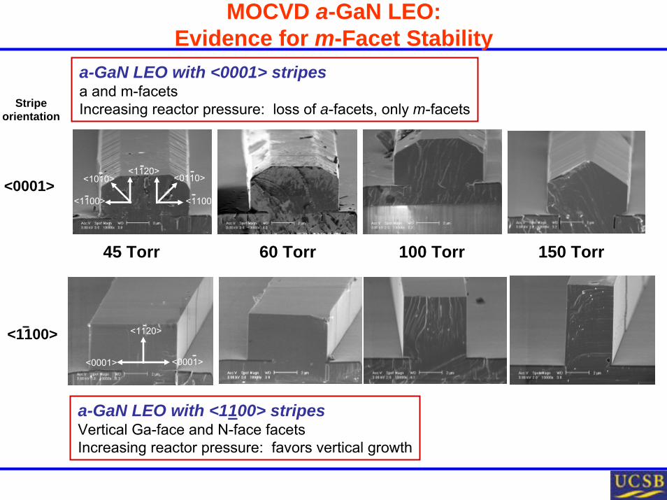
MOCVD a-GaN LEO:Evidence for m-Facet Stability
a-GaN LEO with <0001> stripesa and m-facetsIncreasing reactor pressure: loss of a-facets, only m-facets
a-GaN LEO with <1100> stripesVertical Ga-face and N-face facetsIncreasing reactor pressure: favors vertical growth
45 Torr 60 Torr 100 Torr 150 Torr
<1100>
<0001>
<1120>
<0001><0001>
Stripe orientation
<0110><1120>
<1100>
<1010>
<1100>

Planar HVPE m-GaN on LiAlO2
• Surfaces characterized by long-range textures, peak to valley < 200 nm.• Near complete elimination of bulk, crystallographic defects.
Free-standing m-GaN:

LED on planar m-GaN
MQW parameters:4 nm InGaN well, 16 nm GaN:Si barrier
LED structure grown by MOCVD on ~250 µm thick HVPE free-standing m-GaN
n-GaN: 2.2 μm (3 x 1018 cm-3)p-GaN: 0.3 μm (6 x 1017 cm-3)n-contact: Al/Au (30/200 nm)p-contact: Pd/Au (20/200 nm)

Polarized Light Emission – EL – m-plane GaN LEDs

• Low gate leakage [1,2,3]
• Low contact resistance [1,2,3]
• Enhancement mode operation [1,2,3]
• Enhanced back barrier confinement [1,2,3]
• InN channel [4]
[1] S. Rajan et al., Jpn. J. Appl. Phys. 44 (2005) L1178.[2] S. Rajan et al., 32nd International Symposium on Compound Semiconductors (ISCS), Sept 18-22 (2005), Europa- Park Rust, Germany[3] S. Rajan, Ph.D. Thesis, University of California at Santa Barbara (2006). [4] K. Xu et al., Appl. Phys. Lett. 83, 251 (2003).
Advantages of N-face GaN for HEMTs

Ga-face
N-face
Courtesy: S. Rajan
Advantages of N-Face GaN for HEMTs

Outline
Background on GaN symmetry and propertiesCrystal symmetryPhysical properties: heterostructures
A-plane and M-plane growthCommon MicrostructureDefect reductionDopingDevices
Semi-polar GaNNew orientations and possibilities
N-face GaNTurning the crystal and devices upside down …

Epitaxial Relationship
– a-GaN (1120) growth surface – GaN c-axis aligns with sapphire c-axis projection
• Convergent beam electron diffraction (CBED) determined polarity
XRD 2θ−ω

Research accomplishments – Non-polar GaN
2001 2002 2003 2004 2005 2006
1st planarHVPEa-GaN
Blue LED onHVPE a-GaN
1st HVPEa-GaN LEO
1st LED onm-GaN
1st MOCVDa-GaN
Advanceda-GaN LEO
1st HVPEm-GaN LEOMOCVD
a-GaN ona-SiC
MBE a-GaNgrowth diagram
Highly p-dopedMBE m-GaNPlanar HVPE
m-GaN
1st MOCVDa-GaN LEO

AlGaN
GaN
+ + + + + + + + + +
+ + + + + + + + + +
- - - - - - - - - - - - - - -Ga-polar surface
- - - - - - - - - - - - - - -2DEG
AlGaN
GaN
- - - - - - - - - - - - - - -
- - - - - - - - - - - - - - -
GaN+ + + + + + + + + +
N-polar surface
+ + + + + + + + + + - - - - - - - - - - - - - - -2DEG
+ + + + + + + + + +
AlGaN- - - - - - - - - - - - - - -
+ + + + + + + + + +
• N-face HEMT demonstrated promising performance
2DEG in excess of 1013 cm-2 with mobility of 1300 cm2/Vs [1]
ft and fmax of 12 GHz and 26 GHz respectively [2]
[1] S. Rajan et al., 47th Electronic Materials Conference, June 2005, Santa Barbara, CA [2] A. Chini et al., 63rd Device Research Conference, Conference Digest pp. 63-64.
AlGaN/GaN Heterostructures

Non-Polar – Common Microstructure
Systems•a-GaN / r-Al2O3 (MOCVD, HVPE and MBE)•a-GaN / a-SiC (MOCVD, MBE, MBE → HVPE)•m-GaN / m-SiC (MOCVD and MBE, MBE → HVPE)•m-GaN / (001) LiAlO2 (HCPE, MBE → HVPE)
TD density (total): ~1x1010 cm-2
SF density (total): >1x105 cm-1
SFs associated with exposed N face (000-1) during early growth
SolutionsIn situ/ex situ nanomaskingLateral Epitaxial Overgrowth (LEO)Two-step Lateral Epitaxial OvergrowthSidewall LEO (SLEO)‘Bulk’ GaN

• Under the current LEO growth conditions…– [0001] symmetric stripe – mixture of vertical and inclined m-planes– [1102] asymmetric stripe – vertical and inclined sidewalls– [1100] rectangular x-sections with vertical c-plane sidewalls
Scale bar = 5 μm (window width)
Inclined-view SEM
LEO Stripe Morphology

Cathodoluminescence (CL)
– uniform luminescence from overgrowth of [1100] stripes
– ‘mottling’ extends across width of [0001] stripes
Scale bar = 5 µm (window width)
CLλ = 365 nm
SEM
[0001][1100]

a-plane GaN/AlGaN MQWs
10-period GaN / AlxGa1-xN MQWs regrown on a-GaN (and c-GaN) templates via MOCVD
•Regrowth conditions modeled after HT epitaxial growth conditions– Tgrowth ~ 1120°C– Preactor = 76 Torr

a-plane vs. c-plane MQWs
•a- and c-plane MQWs simultaneously grown with varying well width
a- and c-MQW dimensions and xAl agree within 7%inferior a-MQW interface quality
a-plane69Å GaN /
96Å Al0.16GaN
c-plane72Å GaN /
98Å Al0.16GaN

PL Emission vs. Well Width
•MQW emission red-shifts with increasing GaN well width– a-plane: redshifts up to the GaN band edge– c-plane: redshifts beyond the GaN band edge
a-MQWc-MQW

MQW Emission Energy
– a-MQW emission modeled using square well SCPS calculations
• exciton binding energy accounts for model overestimation
•‘Nonpolar’ MQWs NOT Affected by Internal Electric Fields

m-GaN on m-SiC: MBE

m-GaN MBE: [Mg] vs. III-V Ratio
Substrate Temp ~ 530 °C on T.C.
REGIME Ga BEP [Torr]Ga-rich 3.3E-7Intermediate 2.4E-7III/V = 1 ~2.26e-7N-rich 1.54E-7
Doped Layers ~100 nm thick
AlGaN marker layers ~10 nm thick.
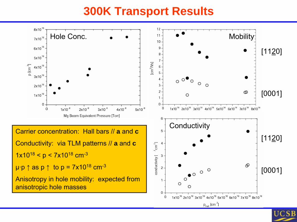
300K Transport Results
Hole Conc. Mobility
[1120]
[0001]
[0001]
[1120]
ConductivityCarrier concentration: Hall bars // a and c
Conductivity: via TLM patterns // a and c
1x10¹⁸ < p < 7x1018 cm-3
µ·p ↑ as p ↑ to p = 7x1018 cm-3
Anisotropy in hole mobility: expected from anisotropic hole masses

Range of dislocation density for which CL images shown in previous slide
Luminescence intensity is proportional to excess minority carrier concentration.
Excess Minority Carrier Concentration: Diffusion Length and Dislocation Density
J.S. Speck and S.J. Rosner, Physica B 274. 24 (1999)
GaN: Minority carrier diffusion length: ~ 100 nm (common)TDs are a limiting factor in non-polar LED performance

The beginning …
The first planar non-polar orientedwurtzite films …

Reactor Pressure - MOCVD
• Reactor Pressure: important growth variable
Reactor pressures ~76 Torr required for planar film growth
76 Torr 300 Torr 600 Torr
inclined-viewSEM
plan-viewSEM

Crystal Mosaic – a-GaN on r-Al2O3
• a-GaN on r-sapphire: orientation-dependent crystal tilt mosaic
omega rocking curves
c-mosaic = 0.28° (Δc/c ~1.1%)m-mosaic = 0.62° (Δa/a ~13.8%)

– LEO stripe morphology dependent on stripe orientation• Analyzed using ‘wagon wheel’ mask
– Three primary orientations: [0001], [1102], [1100] (0°, 45°, 90°)
plan-viewSEM
LEO Orientation Analysis

Dislocation Reduction – AFM
– characteristic surface pits in window regions– “pit-free” overgrowth
•AFM pits decorate TD terminations•One-to-one pit-to-TD correspondence (AFM and TEM)
[1100]
AFM
Mono-CL

AFM TEM
Planar HVPE a-GaN
• Planar Surface decorated with high pit density.
• Faint ~1 nm steps oriented normal to <0001>.
• RMS roughness ~1 nm.TDD: ~ 1 x 1010 cm-2
SFD: ~ 4 x 105 cm-1
Partial TDs: 7x109 cm-2
g = 0002
g = 1010

HVPE LEO a-GaN
• <1100> stripes have vertical c-plane sidewalls.• Ga-face (0001) lateral growth rate ~6x N-face (0001) growth rate.
– Coalescence front offset towards windows (large defect-free wing area results)
Schematic Cross-Sectional SEM Image“Wagon Wheel” pattern

HVPE LEO a-GaN (cont.)
• Typical stripe patterns: 2 µm windows/8 µm wings (2/8), 5/5, and 5/15.
• Asymmetrical {0001} wing growth rates • TDD of < 3 × 10⁻⁶ cm-2 and SFD of < 10-3 cm-1 in
wings; no measurable wing tilt.• Four-fold increase in cathodoluminescence intensity
in wings versus windows.
Coalescence Front
N-Face Wing Ga-Face Wing
SEM Image365 nm CL Image
Inv. DomainsWindow
Ga-FaceWing
N-FaceWing

– a-AlN and a-GaN orientations match the a-SiC
smooth a-GaN surface morphology
AFM
XRD 2θ−ω
a-GaN on a-SiC: Morphology & Orientation

a-GaN on a-SiC: Crystal Mosaic
– Minimal tilt mosaic orientation dependence• c-mosaic greater than m-mosaic
XRD ω rocking curves
c-mosaic = 0.30° (Δc/c ~ -2.8%)m-mosaic = 0.27° (Δa/a ~ -3.4%)

a-GaN on a-SiC: Morphology
– m-Axis rows of coalesced GaN islands coalesce slowly along the c-axis
– Coalesced GaN surfaces feature:
• Undulations along the m-axis
• Low density of submicron pits
• Crystallographic terraces perpendicular to c-axis

a-GaN on a-SiC: N-face Surfaces
• Exposed N-face facets responsible for basal plane faulting
SEM – 100 nm GaN

Planar m-GaN (cont.)
• Threading dislocation density ~ 4 × 109 cm-2.• Basal plane stacking fault density ~ 1 × 105 cm-1.• Possible inhomogeneous distribution of TDs and SFs may explain surface
morphology variations.
AFM TEM

HVPE LEO of m-GaN
• Planar direct-growth films:– Lattice mismatch, island coalescence ⇒ threading dislocations.– Exposed (0001) planes in island/3D growth ⇒ basal plane stacking faults
• Lateral epitaxial overgrowth:– Mask geometry affects growth direction.– Natural growth habit: growth on m-planes preferred.– <1120>-oriented stripes (a-direction) ⇒ Growth on (0001) and (0001) planes (vertical sidewalls)
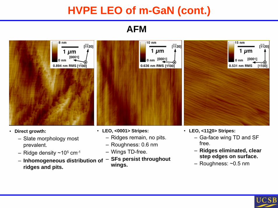
HVPE LEO of m-GaN (cont.)
• Direct growth:– Slate morphology most
prevalent.– Ridge density ~105 cm-1
– Inhomogeneous distribution of ridges and pits.
• LEO, <0001> Stripes:– Ridges remain, no pits.– Roughness: 0.6 nm– Wings TD-free.– SFs persist throughout
wings.
• LEO, <1120> Stripes:– Ga-face wing TD and SF
free.– Ridges eliminated, clear
step edges on surface.– Roughness: ~0.5 nm
AFM

n-Type Doping of a-GaN • a-GaN on a-SiC:
– Undoped GaN is resistive– n increases with Si/Ga ratio for n > 1 x 1018 cm-3
– Residual acceptor concentration on the order of 1 x 1018 cm-3
– Acceptors related to dislocations, stacking faults, and point defects– µ increases with n (screening of defects)
– at n = 1.5 x 1019 cm-3, μ = 109 cm2/V⋅s
Si/Ga
0 1e-4 2e-4 3e-4 4e-4
μ 300Κ
[c
m2 / V
s ]0
20406080
100120
n
[cm
-3]
0
1e+19
2e+19
resistive
N.G. Weimann et al. J. Appl. Phys.83 (1998) 3656

p-Type Doping of a-GaN • a-GaN on r-sapphire:
100 150 200 250 300
4.0x10¹⁹
6.0x10¹⁹
8.0x10¹⁹
1.0x10²⁰
1.2x10²⁰
1.4x10²⁰
Mg effective flow (sccm)M
g co
ncen
trat
ion
(cm
-3)
2x10¹⁷
3x10¹⁷
4x10¹⁷
5x10¹⁷
6x10¹⁷
7x10¹⁷
Hole concentration (cm
-3)
100 150 200 250 30002468
101214
Res
istiv
ity (Ω
-cm
)
Mg Effective Flow (sccm)
• [Mg] tracks Cp2Mg effective flow
• Reduction in hole concentration: • Incorporation of Mg in electrically
inactive form (e.g. precipitates)• Formation of Mg-induced
compensating defects
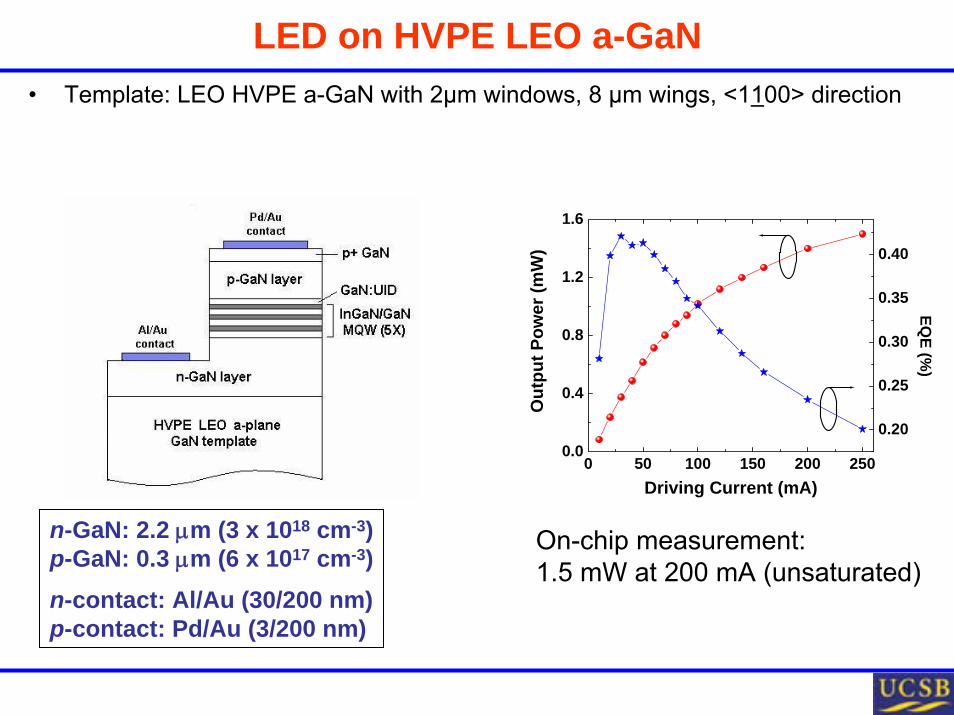
LED on HVPE LEO a-GaN
n-GaN: 2.2 μm (3 x 1018 cm-3)p-GaN: 0.3 μm (6 x 1017 cm-3)n-contact: Al/Au (30/200 nm)p-contact: Pd/Au (3/200 nm)
• Template: LEO HVPE a-GaN with 2µm windows, 8 µm wings, <1100> direction
0 50 100 150 200 2500.0
0.4
0.8
1.2
1.6
Driving Current (mA)
Out
put P
ower
(mW
)
0.20
0.25
0.30
0.35
0.40
EQE (%
)
On-chip measurement:1.5 mW at 200 mA (unsaturated)

• Electroluminescence vs. current: no shift in peak position, little peak linewidthbroadening
– No quantum-confined Stark Effect present
300 400 500 600 7000
1000
2000
3000
a-GaN LED ELEL
Inte
nsity
(a. u
.)
Wavelength (nm)
10 mA 20 mA 50 mA 80 mA 200 mA
0 50 100 150 200 250
23.5
24.0
24.5
25.0
25.5
26.0
26.5
27.0
27.5
Line
wid
th (n
m)
Driving Current (mA)
• MOCVD 5-QW LED on 250 µm free-standing planar HVPE m-GaN
0 50 100 150 200448
450
452
454
456
458
460
462
LED on planar m-GaN (cont.)
EL E
mis
sion
Wav
elen
gth
(nm
)
Drive Current (mA)
0 50 100 150 200
(b)
Current Density (A/cm2)
400 500 600
1000
2000
3000
4000 (a)100 mA80 mA60 mA40 mA30 mA20 mA5 mA
EL In
tens
ity (a
. u.)
Wavelength (nm)
• Turn-on voltage: 3-4 V• Low on series resistance: 16 Ω• Ideality factor ~4• EL emission at 450 nm• Peak shift observed at low current
densities due to band filling

Unpackaged m-GaN LED Results
0 50 100 150 200 250 300
0.0
0.5
1.0
1.5
2.0
2.5
3.0
Drive Current (mA)
CW
Out
put P
ower
(mW
)
0.32
0.34
0.36
0.38
0.40
0.42
0.44
EQE
(%)
0 200 400 600 800 1000
0
2
4
6
8
10
Onw
afer
Out
put P
ower
(mW
)
Drive Current (mA)
1% Duty Cycle (500 ns pulse) 5% Duty cycle (2.5 ms pulse) CW
• cw on-wafer output power at 300 mA : 2.95 mW (0.24 mW @ 20 mA)• Max EQE of 0.43% at 30 mA drive current• Saturation in output power not observed for higher cw drive currents
• Pulsed on-wafer output power at 1 A for 5% duty cycle: 8.5 mW

Packaged m-GaN LED Results
m-GaN LED Lamp Integrated Power
0
1
2
3
4
5
6
0 50 100 150 200
Current [mA]
Inte
grat
ed P
ower
[mW
]
First LED Lamp on Free-Standing m-GaN Substrate
0.0E+00
2.0E-05
4.0E-05
6.0E-05
8.0E-05
1.0E-04
1.2E-04
1.4E-04
1.6E-04
300 400 500 600 700 800
Wavelength [nm]
Pow
er D
ensi
ty [W
/nm
]
1mA2mA3mA5mA10mA15mA20mA30mA40mA50mA60mA70mA80mA90mA100mA120mA140mA160mA180mA200mA
• Unoptimized chip packaged in standard T05 package• Integrated optical power measured in integrating sphere• Approx. 6 mW at 200 mA• Same slight emission peak shift vs. current, as for on-wafer testing


![Exposing GAN-synthesized Faces Using Landmark Locations · obtained using recent GAN-based methods [7, 8]. The increasing sophistication of GAN-synthesized images also has the negative](https://img.dokumen.tips/doc/110x75/5f73a29978e68928974ed632/exposing-gan-synthesized-faces-using-landmark-locations-obtained-using-recent-gan-based.jpg)