Embed Size (px)
Citation preview

Portland State UniversityPDXScholar
Dissertations and Theses Dissertations and Theses
6-6-2018
New Approaches for Memristive Logic ComputationsMuayad Jaafar AljafarPortland State University
Let us know how access to this document benefits you.Follow this and additional works at: https://pdxscholar.library.pdx.edu/open_access_etds
Part of the Electrical and Computer Engineering Commons
This Dissertation is brought to you for free and open access. It has been accepted for inclusion in Dissertations and Theses by an authorizedadministrator of PDXScholar. For more information, please contact [email protected].
Recommended CitationAljafar, Muayad Jaafar, "New Approaches for Memristive Logic Computations" (2018). Dissertations and Theses. Paper 4372.
10.15760/etd.6256

New Approaches for Memristive Logic Computations
by
Muayad Jaafar Aljafar
A dissertation submitted in partial fulfillment of the requirements for the degree of
Doctor of Philosophy in
Electrical and Computer Engineering
Dissertation Committee: Marek A. Perkowski, Chair
John M. Acken Xiaoyu Song Steven Bleiler
Portland State University 2018

© 2018 Muayad Jaafar Aljafar

i
Abstract
Over the past five decades, exponential advances in device integration in
microelectronics for memory and computation applications have been observed. These
advances are closely related to miniaturization in integrated circuit technologies. However,
this miniaturization is reaching the physical limit (i.e., the end of Moore’s Law). This
miniaturization is also causing a dramatic problem of heat dissipation in integrated circuits.
Additionally, approaching the physical limit of semiconductor devices in fabrication
process increases the delay of moving data between computing and memory units hence
decreasing the performance. The market requirements for faster computers with lower
power consumption can be addressed by new emerging technologies such as memristors.
Memristors are non-volatile and nanoscale devices and can be used for building memory
arrays with very high density (extending Moore’s law). Memristors can also be used to
perform stateful logic operations where the same devices are used for logic and memory,
enabling in-memory logic. In other words, memristor-based stateful logic enables a new
computing paradigm of combining calculation and memory units (versus von Neumann
architecture of separating calculation and memory units). This reduces the delays between
processor and memory by eliminating redundant reloading of reusable values. In addition,
memristors consume low power hence can decrease the large amounts of power dissipation
in silicon chips hitting their size limit.
The primary focus of this research is to develop the circuit implementations for logic
computations based on memristors. These implementations significantly improve the
performance and decrease the power of digital circuits. This dissertation demonstrates in-

ii
memory computing using novel memristive logic gates, which we call volistors (voltage-
resistor gates). Volistors capitalize on rectifying memristors, i.e., a type of memristors with
diode-like behavior, and use voltage at input and resistance at output. In addition,
programmable diode gates, i.e., another type of logic gates implemented with rectifying
memristors are proposed. In programmable diode gates, memristors are used only as
switches (unlike volistor gates which utilize both memory and switching characteristics of
the memristors). The programmable diode gates can be used with CMOS gates to increase
the logic density. As an example, a circuit implementation for calculating logic functions
in generalized ESOP (Exclusive-OR-Sum-of-Products) form and multilevel XOR network
are described. As opposed to the stateful logic gates, a combination of both proposed logic
styles decreases the power and improves the performance of digital circuits realizing two-
level logic functions Sum-of-Products or Product-of-Sums.
This dissertation also proposes a general 3-dimentional circuit architecture for in-
memory computing. This circuit consists of a number of stacked crossbar arrays which all
can simultaneously be used for logic computing. These arrays communicate through
CMOS peripheral circuits.

iii
Dedication
Seek knowledge from the cradle to the grave, Prophet Muhammad.
To Noor, with love
To Mustafa and Murtaza
To my parents

iv
Acknowledgements
I would like to thank my advisor, Dr. Marek Perkowski. He has been supportive since
the days I began to learn about the basics of this research. My dissertation committee
guided me through all these years. Thank you to John Acken, Xiaoyu Song and Steven
Bleiler. Specially, I thank Dr. John Acken for patient guidance, encouragement and advice.
I thank my family. Their support has been unconditional all these years; they have given
up many things for my success; they have cherished with me every great moment and
supported me whenever I needed it.
Last and certainly not least, I thank the higher committee for education development in
Iraq (HCED-Iraq) for their generous support.
v
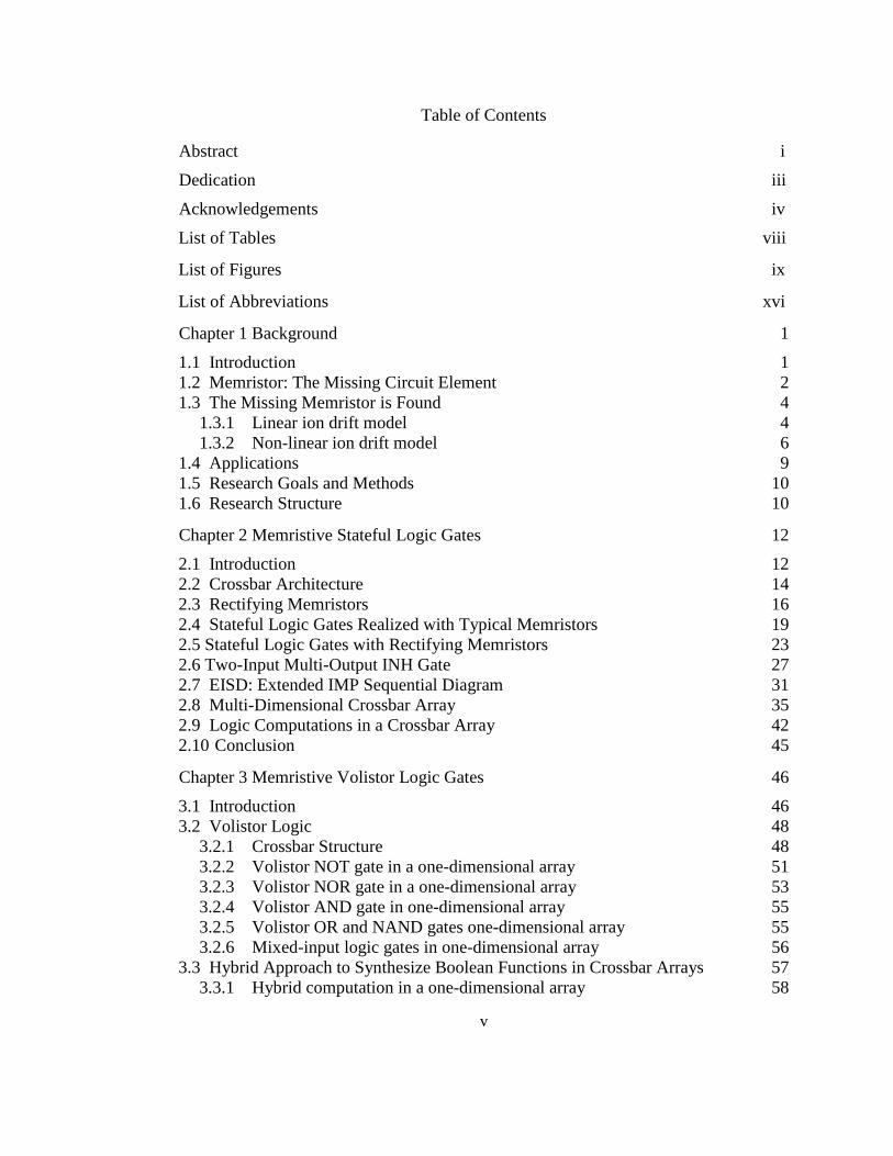
Table of Contents
Abstract i
Dedication iii
Acknowledgements iv
List of Tables viii
List of Figures ix
List of Abbreviations xvi
Chapter 1 Background 1
1.1 Introduction 1
1.2 Memristor: The Missing Circuit Element 2
1.3 The Missing Memristor is Found 4
1.3.1 Linear ion drift model 4
1.3.2 Non-linear ion drift model 6
1.4 Applications 9
1.5 Research Goals and Methods 10
1.6 Research Structure 10
Chapter 2 Memristive Stateful Logic Gates 12
2.1 Introduction 12
2.2 Crossbar Architecture 14
2.3 Rectifying Memristors 16
2.4 Stateful Logic Gates Realized with Typical Memristors 19
2.5 Stateful Logic Gates with Rectifying Memristors 23
2.6 Two-Input Multi-Output INH Gate 27
2.7 EISD: Extended IMP Sequential Diagram 31
2.8 Multi-Dimensional Crossbar Array 35
2.9 Logic Computations in a Crossbar Array 42
2.10 Conclusion 45
Chapter 3 Memristive Volistor Logic Gates 46
3.1 Introduction 46
3.2 Volistor Logic 48
3.2.1 Crossbar Structure 48
3.2.2 Volistor NOT gate in a one-dimensional array 51
3.2.3 Volistor NOR gate in a one-dimensional array 53
3.2.4 Volistor AND gate in one-dimensional array 55
3.2.5 Volistor OR and NAND gates one-dimensional array 55
3.2.6 Mixed-input logic gates in one-dimensional array 56
3.3 Hybrid Approach to Synthesize Boolean Functions in Crossbar Arrays 57
3.3.1 Hybrid computation in a one-dimensional array 58

vi
3.3.2 Hybrid computation in a two-dimensional array 61
3.3.3 Hybrid computation in a crossbar network 64
3.4 Volistor Logic Power Consumption 71
3.4.1 Power analysis and switching delay in a 1 × 8 crossbar array for S1 > 0 74
3.4.2 Power analysis in a 1 × 8 crossbar array for S1 = 0 76
3.4.3 Power analysis and switching delay in a 1×64 Crossbar Arrays for S1 > 0 80
3.5 Summary and Conclusion 84
Chapter 4 Memristive Programmable Diode Logic Gates 86
4.1 Implementation Approach 86
Chapter 5 A Time-Efficient CMOS-Memristive Programmable Circuit Realizing Logic
Functions in Generalized AND-XOR Structures 91
5.1 Introduction 92
5.2 A Generalized ESOP Structure 95
5.3 The mPLD-XOR: Circuit Structure and Functionality 98
5.4 Programming the mPLD-XOR 102
5.5 Implementation Example in the mPLD-XOR 103
5.5.1 A 3-bit adder 104
5.5.2 A 3-bit multiplier 111
5.6 Evaluation and Comparison of Different Logic Styles 114
5.7 Conclusion 117
Chapter 6 Multi-Input Volistor XNOR Gates 120
6.1 Introduction 120
6.2 Review of Rectifying Memristors, Volistors, and Programmable Diode Gates 122
6.2.1 Rectifying memristors 122
6.2.2 Volistor logic 123
6.2.3 Memristive diode logic 123
6.3 Two-Input Volistor XNOR Gate 124
6.3.1 Setting operation 125
6.3.2 Write operation 125
6.3.3 Read operation 126
6.3.4 Circuit simulation 126
6.4 N-input Volistor XNOR Gate 130
6.5 Summary and Conclusion 132
Chapter 7 Volistor Logic Gates in Crossbar Arrays of Rectifying Memristors 134
7.1 Introduction 134
7.2 Circuit Structure for Volistor Logic Gates 137
7.3 Review of Volistor Gates in One-Dimensional Arrays 139
7.3.1 Volistor NOR gate 140
7.3.2 Input-volistor NOR gate 141
7.4 Volistor Gates in Two-Dimensional Arrays 143

vii
7.4.1 Improved volistor NOR gate 143
7.4.2 Deselect of volistor NOR gate 145
7.4.3 Volistor AND gate 147
7.4.4 Volistor COPY gate 149
7.5 Input-Volistor Gates in Two-Dimensional Arrays 150
7.5.1 Input-volistor INH gate 150
7.5.2 Input-volistor AND gate 151
7.6 Design Constraints of Volistor gates in Crossbar Arrays 151
7.6.1 Design constraints of improved volistor NOR gate 151
7.6.2 Design constraints of input-volistor NOR gate 154
7.6.3 Design constraints of input-volistor AND gate 156
7.7 Implementation Example and Comparisons 157
7.7.1 Memristive programmable diode gates 158
7.7.2 Realization of a multi-output AND-OR function in the mPLA 159
7.7.3 Comparisons of the mPLA implementations 160
7.8 Conclusion 165
Chapter 8 Memristive Circuit Architectures 166
8.1 Memristive Circuit Architecture for Logic Computations 166
Chapter 9 Summary, Conclusion, Achievements, and Future Work 172
9.1 Summary and conclusion 172
9.2 Achievements and publications 175
Terminal References 177
Appendix Power Properties 184
viii
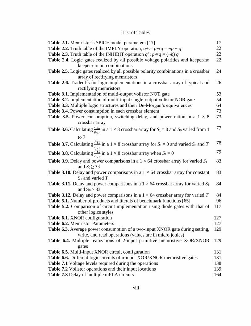
List of Tables
Table 2.1. Memristor’s SPICE model parameters [47] 17
Table 2.2. Truth table of the IMPLY operation, q+:= p→q = ¬p + q 22
Table 2.3. Truth table of the INHIBIT operation q+: p↛q = (¬p) q 22
Table 2.4. Logic gates realized by all possible voltage polarities and keeper/no
keeper circuit combinations
22
Table 2.5. Logic gates realized by all possible polarity combinations in a crossbar
array of rectifying memristors
24
Table 2.6. Tradeoffs for logic implementations in a crossbar array of typical and
rectifying memristors
26
Table 3.1. Implementation of multi-output volistor NOT gate 53
Table 3.2. Implementation of multi-input single-output volistor NOR gate 54
Table 3.3. Multiple logic structures and their De-Morgan’s equivalences 64
Table 3.4. Power consumption in each crossbar element 73
Table 3.5. Power consumption, switching delay, and power ration in a 1 × 8
crossbar array
73
Table 3.6. Calculating 𝑃𝑆𝐿
𝑃𝑉𝐿 in a 1 × 8 crossbar array for S1 = 0 and S0 varied from 1
to 7
77
Table 3.7. Calculating 𝑃𝑆𝐿
𝑃𝑉𝐿 in a 1 × 8 crossbar array for S1 = 0 and varied S0 and T 78
Table 3.8. Calculating 𝑃𝑆𝐿
𝑃𝑉𝐿 in a 1 × 8 crossbar array when S1 = 0 79
Table 3.9. Delay and power comparisons in a 1 × 64 crossbar array for varied S1
and S0 ≥ 33
83
Table 3.10. Delay and power comparisons in a 1 × 64 crossbar array for constant
S1 and varied T
83
Table 3.11. Delay and power comparisons in a 1 × 64 crossbar array for varied S1
and S0 > 33
84
Table 3.12. Delay and power comparisons in a 1 × 64 crossbar array for varied T 84
Table 5.1. Number of products and literals of benchmark functions [65] 96
Table 5.2. Comparison of circuit implementation using diode gates with that of
other logics styles
117
Table 6.1. XNOR configuration 127
Table 6.2. Memristor Parameters 127
Table 6.3. Average power consumption of a two-input XNOR gate during setting,
write, and read operations (values are in micro joules)
129
Table 6.4. Multiple realizations of 2-input primitive memristive XOR/XNOR
gates
129
Table 6.5. Multi-input XNOR circuit configuration 131
Table 6.6. Different logic circuits of n-input XOR/XNOR memristive gates 131
Table 7.1 Voltage levels required during the operations 138
Table 7.2 Volistor operations and their input locations 139
Table 7.3 Delay of multiple mPLA circuits
164

ix
List of Figures
Figure 1.1. Four fundamental passive circuit elements [Redrawn from 2]. 2
Figure 1.2. i-v characteristic of the memristor for a rectangular pulse input. (Left)
Input voltage applied across the memristor. (Right) hysteresis
behavior of the memristor.
4
Figure 1.3. (a) Structure of the HP example of memristor. (b) Circuit equivalent.
[Redrawn from 2]
5
Figure 1.4. The schematic of memristive device realized using tunnel barrier
where w and Rs represent the state variable and the electroformed
channel resistor [Redrawn from 12].
8
Figure 2.1. Idealized hysteretic behavior of the memristor in the i-v plane. VCLOSE
and VOPEN are threshold voltages, and VSET and VCLEAR are
programming voltages.
13
Figure 2.2. Schematic diagram of a 1 × 2 crossbar array. The instant application
of voltage pulses VCOND and VPROG to switches P and Q,
respectively, may toggle the logic state of Q depending on the initial
state of P and Q.
16
Figure 2.3. Characteristics of a rectifying memristor. (Left) The i-v characteristic
of the memristor. (Right) The s-v characteristic of a memristor. The
diagrams are depicted using the LTspice simulator and the
memristor model in [47].
18
Figure 2.4. Schematic of a keeper circuit [Redrawn from 48]. VW denotes the
voltage on W.
25
Figure 2.5. Schematic of a 1 × 9 crossbar array of rectifying memristors for
computing function F.
28
Figure 2.6. Schematic of memristive computing circuit including control and
datapath units.
30
Figure 2.7. (Left) Schematic of a computational array connected to driver
circuitries. (Right) Schematic of each driver circuitry.
31
Figure 2.8. Symbolic diagram of a 2-input IMP gate in ISD notation. 31
Figure 2.9. ISD of function NAND (p, q) where the output is stored as a new state
of memristor R.
32
Figure 2.10. Symbolic diagram of a two-input INH gate in EISD notation. 32
Figure 2.11. EISD of NOR gate. Different EISD notations for r = NOR (p, q)
depending on source and target memristors locations.
33
Figure 2.12. EISD of multi-output function OR 𝑝, 𝑞 ↛ 𝑟,OR 𝑝, 𝑞 ↛ 𝑠. 33
Figure 2.13. EISD of XOR (p, q) = [[(p↛q) + (q↛p)] ↛1] ↛1. 33
Figure 2.14. EISD notation of XOR (p, q, r). (a) The XOR gate is implemented
with 15 operations and five memristors. (b) The XOR gate is
implemented with 16 operations and four memristors. The EISD
shows the trade-off between the number of memristors and the
operations.
34

x
Figure 2.15. A 3 × 3 crossbar array of non-rectifying memristors. 37
Figure 2.16. Half-select problem may cause sneak current paths. The green dash-
line represents the desired current path whereas the red dash-lined
represents an undesired sneak current path.
37
Figure 2.17. (a) The sneak path disturbs the READ and WRITE operations. (b)
The circuit equivalent of the crossbar array with sneak path
phenomenon.
37
Figure 2.18. Biasing schemes for READ and WRITE operation. These schemes
limit the sneak path currents.
39
Figure 2.19. The effect of nonzero resistance of wires on the READ and WRITE
operations.
40
Figure 2.20. Schematic of the complete memristor crossbar array. The driver
circuitries are illustrated in Fig. 2.7.
41
Figure 2.21. Symbolic matrix. The entities show the values of the crossbar
memristors.
43
Figure 2.22. Symbolic matrices illustrate the steps of computing XOR (p, q, r) with
INH gates. The number of operations (clock cycles) to implement
the XOR gate is 11.
43
Figure 3.1. Crossbar arrays. (a) 1 × 2 crossbar array. (b) 2 × 1 crossbar array. The
inset shows the symbolic diagram of a memristor. The flow of
current into the device, as shown above, increases the resistance.
49
Figure 3.2. Symbolic illustration of a driver circuit connected to each wire. 50
Figure 3.3. Symbolic notations for volistor logic gates. (a) Volistor NOT. (b) two-
input volistor NOR gate. (c) two-input volistor AND gate. (d)
mixed-input NOR gate. Inside the gates, symbols V and R denote
whether a signal is a voltage-based or resistance-based,
respectively.
51
Figure 3.4. Volistor NOT behavior. (a) 1 × 8 crossbar array implementing a four-
output NOT and showing arbitrary nature of the locations of source
memristors S and target memristors T. The contribution of each
memristor is determined by the voltage driver, to which it is
connected. Wire W is connected to Z. (b) The operation of a one-
output NOT in a 1 × 2 array. VW stabilizes at ≈ 600 mV indicating
𝑣𝑠= ‘1’ manifesting on W. In addition, t1 toggles to ‘0’. (c) The
operation of a 63-output NOT in a 1 × 64 array. VW stabilizes and t
toggles as in b. (d) The operation of a one-output NOT in a 1 × 2
array. VW stabilizes at ≈ 0V indicating 𝑣𝑠= ‘0’ manifesting on W. As
a result, t remains ‘1’. (e) VW stabilizes as in d.
52
Figure 3.5. A 3 × 1 crossbar array used to implement a two-input volistor NOR. 54
Figure 3.6. Mixed input NOR. The implementation of a three-input one-output
NOR gate. The resistive input is stored in S1 and the voltage inputs
are applied to S2 and S3. The output is stored in memristor T.
56
Figure 3.7. Example of logic computation based on hybrid approach in a crossbar
array. (a) 1 × 4 crossbar array used to implement SOP function f.
60
xi
(b) Circuit configuration to implement each step. The total number
of consecutive operations (pulses) to realize f is 5.
Figure 3.8. Crossbar array. (a) Crossbar array is divided into three sections; gates
in section 1 are implemented with volistors but in section 2 and 3
are realized with stateful NOR. (b) The stateful approach realizes
two logic levels. (c) However, the hybrid approach realizes three
logic levels with the same implementation cost of the stateful
approach. Li is the number of logic level.
61
Figure 3.9. Symbolic matrices illustrate the steps of computing f ab cd A
based on the hybrid approach. (a) Initialization step. (b) Computing
ab with volistor AND. (c) Computing cd with volistor AND. (d)
Computing ab cd with stateful NOR. (e) Computing f with
mixed-input NOR.
64
Figure 3.10. Implementation of POS function f in a crossbar network. The function
is realized in a two-step process. (a) Realizing the first logic level
of function f in separate crossbars. This step produces four NOR
gates. (b) Realizing the second logic level of function f in a 16 × 1
crossbar array. This step produces the output of the POS function.
The interconnections and voltages applied to the wires show the
network configuration in each step.
66
Figure 3.11. Implementation of Boolean functions in different logic structures
based on the hybrid approach. (a) Example of a SOP function. (b)
Example of a POS function. (c) Example of a three level sum of
products of sums. (d) Example of an XOR of two products. (e)
Example of a NAND-AND-XOR logic function. (f) Example of an
AND-XOR-OR logic function. ‘P’ stands for pulse (operation),
e.g., 1p indicates one pulse for implementing a logic level. VL and
SL stand for volistor and stateful logic operations. In all circuits,
only the first logic level is implemented with volistor gates.
67
Figure 3.12. Realization of NAND-AND-XOR function f. The function is realized
in a six-step process in four crossbar arrays. (a) The first logic level
is realized with volistors; (b) the second logic level is realized with
mixed-input gates; (c)-(e) the other logic levels are realized with
stateful logic. Wires are set to 0V, v+, or v־ or connected to GND
through load resistor RG or to Z. In each step, the operation is
depicted by symbolic gates, and the results are shown as outputs of
the gates.
71
Figure 4.1. Memristive programmable diode OR gate. (a) A schematic of a two-
input diode OR gate implemented with rectifying memristors. (b)
The behavior of a two-input diode NOR gate. (c) The relation
between the size of a diode NOR gate and its RC delay during the
precharge interval. (d) A schematic of a 100-input diode NOR gate.
(e) The behavior of 100-input diode NOR gate. (f) A schematic of
89
xii
a two-input diode NOR with pull-down transistor. (g) The behavior
of two-input diode NOR with pull-down transistor.
Figure 4.2. Memristive programmable diode AND gate. (a) A schematic of a two-
input diode AND gate implemented with rectifying memristors. (b)
The behavior of a two-input diode NAND gate. (c) Relation
between the size and RC delay of a diode NAND gate during the
charge interval. (d) A schematic of a 100-input diode NAND gate.
(e) The behavior of 100-input diode NAND gate. (f) A schematic
diagram of a two-input diode NAND gate with pull-up resistor. (g)
The behavior of two-input diode NAND with pull-up resistor.
90
Figure 5.1. (a) Schematic of NAND, AND, NOR, OR-XOR logic structure. (b)
Logical equivalence of NAND, AND, NOR, OR-XOR structure
as realized in mPLD-XOR. (c) mPLD-XOR realizes functions in
NOT-OR-XOR-NOT logic structure.
97
Figure 5.2. Function G1 is implemented as its logical equivalence, G2. 97
Figure 5.3. Schematic of the mPLD-XOR. 99
Figure 5.4. Schematic of an mPLD-XOR for realizing an n-input single-output
function with l lines diode OR where l=2n to allow for inputs
complemented. Ini are the primary inputs where i ∈ 1,⋯ , 𝑛, and
Cj are the control signals stored in ReRAM where j ∈ 1,⋯ , 𝑙.
The output of the circuit is Q or Q depending on the function being
implemented.
99
Figure 5.5. Schematic of ReRAM of the mPLD-XOR shown in Figure 5.3 with
the reference resistor Rg.
100
Figure 5.6. Simulation results of the single-output mPLD-XOR shown in Figure
5.4 with the ReRAM configuration shown in Figure 5.5.
101
Figure 5.7. Programming the ReRAM. (a) Initializing the ReRAM to HRS (or
logic ‘0’). (b) Programming the right-most column of the ReRAM.
103
Figure 5.8. Generic fabric of the mPLD-XOR programmed for realizing a 3-bit
adder. The grey rectangles correspond to memristive arrays, the
white rectangles correspond to hybrid CMOS-memristive circuits,
and the rest of the blocks correspond to CMOS circuits.
104
Figure 5.9. Schematic diagram of sub-ReRAMs. Sub-ReRAM (a) stores the
control data for driving CMOS sub-circuits of the mPLD-XOR.
Sub-ReRAMs (b)-(d) store control data for realizing S0 and S1, S2,
and Co, respectively. The number of clock cycles for calculating an
output is shown in parenthesis, e.g., (#8). The size of sub-ReRAMs
is 35 × 8.
109
Figure 5.10. (a)-(j) The computational steps for realizing a 3-bit adder with stateful
gates. The total number of IMP and FALSE operations is 29. In
each step, the numbers of operations are shown.
111
Figure 5.11. Schematic of mPLD-XOR for realizing a 3-bit multiplier. In this
implementation, the number of computational steps is 12, and
instructions occupy 47 × 12 of the ReRAM size.
112

xiii
Figure 5.12. Schematic diagram of a 3-bit multiplier in a six-level-XOR-network
structure with any combination of sums, products, XORs, and
literals at the input of any XOR gate. This circuit is implemented
with the mPLD-XOR with feedback circuit. The internal signals are
stored in the memory cells to decrease the size of the ReRAM.
113
Figure 5.13. 6 × 16 crossbar array used to implement a 3-bit multiplier with
stateful logic gates. The matrix elements denote initial states of
crossbar memristors.
113
Figure 5.14. Area and delay comparisons of an N-bit Adder realized with multiple
approaches.
116
Figure 6.1. The i–v characteristic of a rectifying memristor and its symbolic
diagram. The flow of current into the device, as shown above,
decreases the resistance.
122
Figure 6.2. Implementation of memristive gates. (a) Implementation of two-input
volistor NOR gate. (b) Implementation of a 2-input programmable
diode AND gate.
124
Figure 6.3. Volistor XNOR gate. (a) Schematic of 2-input volistor XNOR gate.
(b) Behavior of volistor XNOR gate.
125
Figure 6.4. Read operation. Non-destructive voltage VREAD is applied to the
volistor XNOR gate to read the output. The inset shows the
symbolic diagram of the XNOR gate.
126
Figure 6.5. XNOR Circuit Simulation. The initial states are (s1, s2) = (0, 0). (a)
The circuit behavior when inputs are (Vin1, Vin2) = (1, 0). (b) The
circuit behavior when inputs are (Vin1, Vin2) = (1, 0). The outputs,
VAND and VOUT, are relevant only during the read operation.
128
Figure 6.6. Schematic diagram of a multi-input volistor XNOR gate. 130
Figure 7.1. General circuit structure for logic computations based on volistor and
stateful gates.
137
Figure 7.2. Schematic of an n-input volistor NOR gate realized in a 1 × (n+1)
memristive array.
141
Figure 7.3. Implementation of a three-input volistor NOR gate with a fan-out of
three. The source memristors are in LRS. Horizontal wires are
connected to high impedance Z.
141
Figure 7.4. (a) Schematic of two-input-volistor NOR gate. Inputs are va and rb,
and the output is rT. (b) Schematic of an n-input-volistor NOR gate
where all of the inputs are logic ‘0’.
142
Figure 7.5. Implementation example of multiple volistor NOR gates in a crossbar
array. The circuit implements Tm = NOR (a, b, c) on wm and Tm+1 =
NOR (¬a, ¬b, ¬c) on wm+1. Source memristors on wm + 2 are in HRS
to disconnect the input voltages.
144
Figure 7.6. Deselecting a volistor gate in a crossbar array. (a) Traditional approach
for deselecting a volistor gate by v+/2 scheme might disturb the
circuit operation. (b) Our approach for deselecting a volistor gate is
to use pass transistors and v+ scheme to ensure the correct operation
of the circuit.
145

xiv
Figure 7.7. Example of four sub-crossbar arrays (A, B, C, and D) connected by a
column and row of pass transistors.
146
Figure 7.8. Implementation of volistor AND gate with input resistances stored in
a computational array. (a) Realization of Tm=AND (a, b, c) where
inputs are located on row wm-1 (b) Realization of Tn = AND (a, b, c)
where inputs are located on column wn-1.
147
Figure 7.9. Volistor COPY Operation. (a) COPY value a on vm-1 to memristor Tm
on vm (b) COPY value a on wn-1 to memristor Tn on wn.
149
Figure 7.10. Schematic of input-volistor INH gate. Inputs are va and rb, and the
output is (¬a) b, which updates resistance state rb of memristor T.
150
Figure 7.11. VT-n relations of multiple volistor NOR gates realized in two m × n
crossbar arrays. The shaded area shows the range of VT for
implementing i-input volistor NOR gates where i ≤ n - 1.
153
Figure 7.12. (a) State transition delay in LRS memristor connected to VCLEAR. (b)
Simulation results of three 50-input volistor NOR gates executed in
a 3×101 crossbar array where 0 × vinh, 1 × vinh, and 50 × vinh show
the number of high inputs applied to each volistor NOR gate. Also,
v1, v2, and v3 denote the voltages on horizontal wires w1, w2 and w3
of volistor NOR gates. And T1, T2, and T3 are the memristances
(resistance states) of target memristors denoting the outputs.
154
Figure 7.13. VT–n relations of multiple input-volistor NOR gates realized in two
m × n crossbar arrays. The shaded area shows the range of VT for
implementing i-input-volistor NOR gates where i ≤ 2n-2.
156
Figure 7.14. VT-m relations of multiple volistor AND gates realized in two m × n
crossbar arrays. The shaded area shows the range of VT for realizing
i-input volistor AND gates where i ≤ 2m - 1.
157
Figure 7.15. Schematic of the mPLA for realizing a multi-output POS function. 159
Figure 7.16. Area estimation of memory array. The graphs show the maximum
size of memory arrays in each mPLA circuit.
164
Figure 8.1. Bock diagram of a memristive circuit for logic computations (upper
view). Logical operations are implemented in the computational
array. The memory arrays store the instructions. Memory arrays
and computational array communicate through CMOS drivers
shown as small rectangles.
167
Figure 8.2. Block diagram of a 3D memristive array (top side view). 168
Figure 8.3. (Left) Schematic of a single CMOS driver in Fig. 8.2. (Right) Driver’s
circuitry.
168
Figure 8.4. Schematic of four stacked computational arrays and their CMOS
drivers (bird view). Outputs of the stacked computational arrays are
beneath the memory arras. The memory arrays are not shown in this
figure.
169

xv
Figure 8.5. (a) Schematic of driver’s interconnections with computational arrays
shown in Fig. 8.2 (bird view) (b) Four stacked CMOS drivers (Bird
view). (c) Schematic of four stacked CMOS drivers which shows
how four wires of four stacked computational arrays communicate
through the drivers (side view).
170
Figure 8.6. CMOS driver for logic computing with hybrid volistor and stateful
logic operations.
171

xvi
List of Abbreviations
Symbol Definition
ASIC Application-Specific Integrated Circuit
3D Array 3-Dimenstional crossbar Array
CMOL CMOS-Molecular scale device
ESOP Exclusive-or-Sum-of-Products
GND Ground node
LRS Low resistance state of a memristor
HRS High resistance state of a memristor
Memristor Memory-resistor
POS Product-of-Sums
PPRM Positive Polarity Reed-Miller
VCOND or
VREAD
Applied to source memristors during the READ operation in stateful
logic
VCLOSE Positive threshold voltage for programming a memristor to LRS
VOPEN Negative threshold voltage for programming a memristor to HRS
VSET Positive programming voltage for abrupt resistance switching (form
HRS to LRS)
VCLEAR Negative programming voltage for abrupt resistance switching (form
LRS to HRS)
VPROG Applied to target memristors while executing stateful gates
VW Voltage on wire W
VS Input voltage applied to a source memristor while executing volistors
VT Applied to a target memristor while executing volistors
VL Volistor logic
SL Stateful logic
PS0 Average power consumption in a source memristor connected to logic
‘0’ (in VL) or set to HRS (in SL)
PS1 Average power consumption in a source memristor connected to logic
‘1’ (in VL) or set to LRS (in SL)
PS Average power consumption in a source memristors during SL or VL
PT Average power consumption in a target memristor
RG Load resistor
PRG Average power consumption in load resistor RG
𝑃𝑆0𝑊𝐿 PS0 (average power consumption in source memristors set to ‘0’) during
VL
𝑃𝑆1𝑊𝐿 PS1 (average power consumption in source memristors set to ‘1’) during
VL
𝑃𝑆𝑊𝐿 PS (average power consumption in source memristors) during VL
𝑃𝑆0𝑆𝐿 PS0 (average power consumption in source memristors in HRS) during
SL

xvii
𝑃𝑆1𝑆𝐿 PS1 (average power consumption in source memristors in LRS) during
SL
𝑃𝑆𝑆𝐿 PS (average power consumption in source memristors) during SL
SOP Sum-of-Products
S0 Number of source memristors in logic ‘0’
S1 Number of source memristors in logic ‘1’
TANT Three-level AND NOT Network with True inputs
Td Switching delay in a memristor
Volistor Voltage-resistor
Z High impedance

1
Chapter 1
Background
1.1 INTRODUCTION
The exponential advances in microelectronics over the past five decades are unlikely to
continue for the next decade due to physical limitations. The density of transistors in each
square centimeter has already exceeded 100 Million. The heat dissipation and memory
access delay are the main problems in these ultra-dense microcomputers. The computing
research community have been challenged to find variables other than charge or voltage,
devices, and architectures that enable the integration to go far beyond the limits of
conventional microelectronics technology [1]. In 2008, researchers in Hewlett Packard
Labs [2] connected the theory of memristor [3] to the thin film devices (TiO2). Memristors
and memristive devices [4] are two terminal nanoscale devices whose characteristics are
explained by the relation between magnetic-flux (𝜑) and charge (q). Memristors and
memristive devices are non-volatile devices that can be used for in-memory computing.
Therefore, memristors can perform advanced computing paradigms of combining
calculation and memory units. Unlike traditional computing paradigms, which separate
calculation from memory, in new computing paradigms there is no problem of memory
access delay and power crisis as one that exists in digital integrated circuits. However,
using this new paradigm of logic computation requires executing long sequences of logic
operations, which in turn increases the power consumption and complicates the control of
the circuit. In this dissertation, this problem is addressed. Multiple solutions are proposed
to decrease the number of in-memory logical operations. The proposed techniques also

2
decrease the power dissipation when compared to other memristive in-memory computing
approaches.
In addition to digital computing, memristors enable analog computing, e.g., in
neuromorphic applications. However, this dissertation only focuses on digital memristive
computing, i.e., memristors are used as binary switches with memory ability.
In this chapter, the theory of memristors, the practical memristors, models and
applications of memristors are briefly described. The goals of this research are also defined.
1.2 MEMRISTOR: THE MISSING CIRCUIT ELEMENT
The circuit elements R, C, L, and M can be functions of v, i, q, and φ in their defining
equations. For example, a charge-controlled memristor is defined as a single-valued
function M (q) [2]. In 1971, Leon Chua reasoned that there should be another fundamental
Fig. 1.1. Four fundamental passive circuit elements [Redrawn from 2].

3
passive circuit element in addition to the resistor, capacitor, and inductor. He called this
new element “memristor”, short for memory-resistor [3]. His reasoning was based on
symmetry arguments where he noted that the number of equations connecting pairs of
circuit variables (electrical current i, voltage v, charge q, and magnetic-flux 𝜑) are six. Two
equations (out of six) are dq = i and dφ = v (Faraday’s law of induction). Other (four)
equations connect pairs of circuit variables via circuit elements. However, before Chua’s
invention, there were only three known circuit element R, L, and C. Chua reasoned the
existence of another circuit element (memristor), which links flux and charge as dφ=Mdq
where M is the memristance of memristor (Fig. 1.1). Note that M is a function of charge,
yielding a nonlinear element. If M were a constant, it would be identical to R. The basic
definition of a current-controlled memristor is shown in (1.1) and (1.2) where w is the state
variable, which is the charge, and R is a state-dependent resistance.
𝑣 = 𝑅(𝑤)𝑖 (1.1)
𝑑𝑤
𝑑𝑡= 𝑖 (1.2)
The memristor concept was generalized in 1976 by Chua and Kang to include a much
broader class of non-linear dynamic systems called memristive system [4]. A memristive
device is a two-terminal passive device whose resistance is a function of state variable w
and the voltage v (or current i) and not on the charge or the flux, directly. The current-
controlled time-invariant memristive devices are described by (1.3) and (1.4).
𝑣 = 𝑅(𝑤, 𝑖)𝑖 (1.3)
𝑑𝑤
𝑑𝑡= 𝑓(𝑤, 𝑖) (1.4)
4
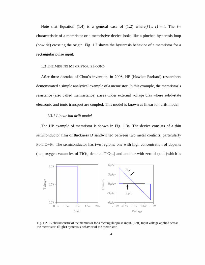
Note that Equation (1.4) is a general case of (1.2) where 𝑓(𝑤, 𝑖) = 𝑖. The i-v
characteristic of a memristor or a memristive device looks like a pinched hysteresis loop
(bow tie) crossing the origin. Fig. 1.2 shows the hysteresis behavior of a memristor for a
rectangular pulse input.
1.3 THE MISSING MEMRISTOR IS FOUND
After three decades of Chua’s invention, in 2008, HP (Hewlett Packard) researchers
demonstrated a simple analytical example of a memristor. In this example, the memristor’s
resistance (also called memristance) arises under external voltage bias where solid-state
electronic and ionic transport are coupled. This model is known as linear ion drift model.
1.3.1 Linear ion drift model
The HP example of memristor is shown in Fig. 1.3a. The device consists of a thin
semiconductor film of thickness D sandwiched between two metal contacts, particularly
Pt-TiO2-Pt. The semiconductor has two regions: one with high concentration of dopants
(i.e., oxygen vacancies of TiO2, denoted TiO2-x) and another with zero dopant (which is
Fig. 1.2. i-v characteristic of the memristor for a rectangular pulse input. (Left) Input voltage applied across
the memristor. (Right) hysteresis behavior of the memristor.

5
only oxide region TiO2). An external voltage bias across the device can drift the charged-
dopants yielding a variable resistance. In other words, the device is analogous to two
variable resistors connected in series as shown in Fig. 1.3b where w (t) represents the state
variable and 0 ≤ w (t) ≤ D. The resistance is RON when w (t) = D, and the resistance is ROFF
when w (t) = 0. Equation (1.5) and (1.6) explain the HP model of memristor where 𝜇𝑉 is
the average ion (vacancies) mobility. Note that Equation (1.5) and (1.6) are derived for the
simplest cases of ohmic electronic conduction and linear ion drift in a uniform field with
average ion mobility 𝜇𝑉.
𝑣(𝑡) = (𝑅𝑂𝑁𝑤(𝑡)
𝐷+ 𝑅𝑂𝐹𝐹 (1 −
𝑤(𝑡)
𝐷)) 𝑖(𝑡) (1.5)
𝑑𝑤
𝑑𝑡= 𝜇𝑉
𝑅𝑂𝑁
𝐷𝑖(𝑡) (1.6)
To keep w (t) within the interval [0, D], it is required to multiply 𝑑𝑤
𝑑𝑡 by window function
as used in [5-7].
text
ROFF
RON
RON (w/D) ROFF (D-w)/D
Undoped
Doped
(a) (b)
Fig. 1.3. (a) Structure of the HP example of memristor. (b) Circuit equivalent. [Redrawn from 2]

6
1.3.2 Non-linear ion drift model
Although the linear ion drift model shows the basic device behaviors, there is a
significant mismatch between the i-v characteristics of this model and that shown in
experiments [8-9]. The linear ion drift model does not represent the non-linear dependence
between 𝑑𝑤
𝑑𝑡 and 𝑖(𝑡). A number of non-linear ion drift models, which is desired for logic
computations, have been proposed. Three examples of non-linear ion drift models are
discussed below.
1) Lehtonen et al. model
Lehtonen et al. [10-11] proposed a model based on experimental results shown in [8]
where the i-v relation is explained by (1.7).
𝑖(𝑡) = 𝑤(𝑡)𝑛𝛽 sinh(𝛼𝑣(𝑡)) + 𝜒[exp (𝛾𝑣(𝑡) − 1] (1.7)
The 𝛼, 𝛽, and 𝛾 are experimental fitting parameters, and n determines the influence of
𝑤(𝑡) on 𝑖(𝑡). The state variable, 𝑤, is normalized within interval [0, 1]. When the device
is in the on-state (𝑤 ≈ 1), 𝑖(𝑡) ≈ 𝑤(𝑡)𝑛𝛽 sinh(𝛼𝑣(𝑡)). When the device is in the off-state
(𝑤 ≈ 0), 𝑖(𝑡) ≈ 𝜒[exp (𝛾𝑣(𝑡) − 1]. The model assumes: 1) asymmetric switching
behavior, and 2) the non-linear dependence between 𝑑𝑤
𝑑𝑡 and 𝑣(𝑡) as explained by (1.8)
where 𝑎 is a constant, 𝑚 is an odd constant, and 𝑓(𝑤) is a windows function.
𝑑𝑤
𝑑𝑡= 𝑎. 𝑓(𝑤). 𝑣(𝑡)𝑚 (1.8)
7
2) Simmons tunnel barrier model
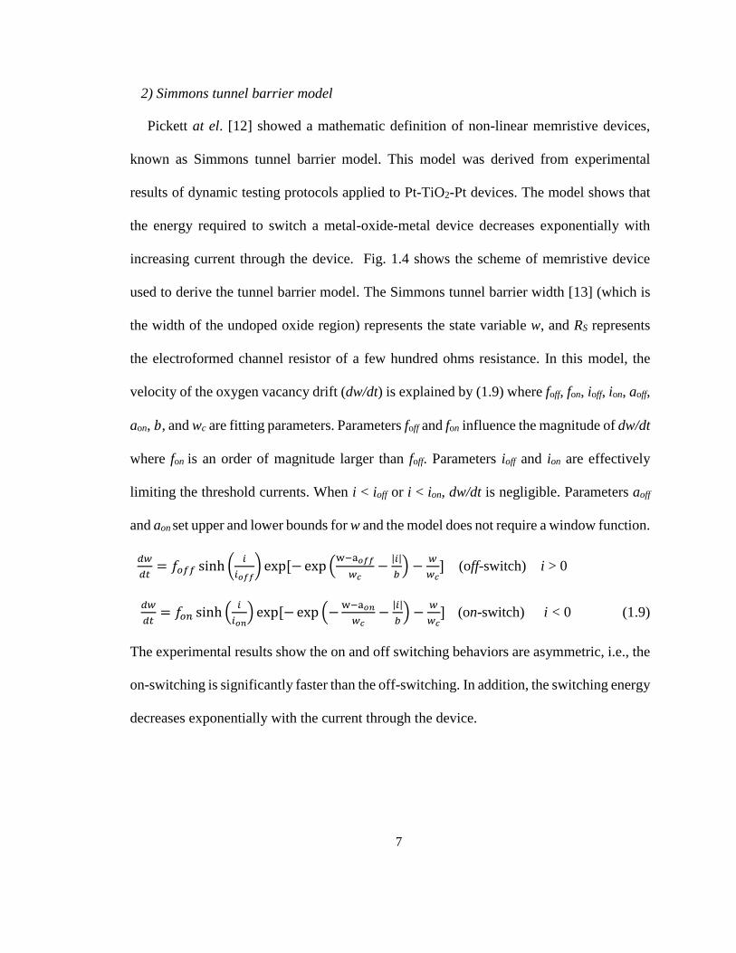
Pickett at el. [12] showed a mathematic definition of non-linear memristive devices,
known as Simmons tunnel barrier model. This model was derived from experimental
results of dynamic testing protocols applied to Pt-TiO2-Pt devices. The model shows that
the energy required to switch a metal-oxide-metal device decreases exponentially with
increasing current through the device. Fig. 1.4 shows the scheme of memristive device
used to derive the tunnel barrier model. The Simmons tunnel barrier width [13] (which is
the width of the undoped oxide region) represents the state variable w, and RS represents
the electroformed channel resistor of a few hundred ohms resistance. In this model, the
velocity of the oxygen vacancy drift (dw/dt) is explained by (1.9) where foff, fon, ioff, ion, aoff,
aon, 𝑏, and wc are fitting parameters. Parameters foff and fon influence the magnitude of dw/dt
where fon is an order of magnitude larger than foff. Parameters ioff and ion are effectively
limiting the threshold currents. When i < ioff or i < ion, dw/dt is negligible. Parameters aoff
and aon set upper and lower bounds for w and the model does not require a window function.
𝑑𝑤
𝑑𝑡= 𝑓𝑜𝑓𝑓 sinh (
𝑖
𝑖𝑜𝑓𝑓) exp [− exp (
w−a𝑜𝑓𝑓
𝑤𝑐−|𝑖|
𝑏) −
𝑤
𝑤𝑐] (off-switch) i > 0
𝑑𝑤
𝑑𝑡= 𝑓𝑜𝑛 sinh (
𝑖
𝑖𝑜𝑛) exp [− exp (−
w−a𝑜𝑛
𝑤𝑐−|𝑖|
𝑏) −
𝑤
𝑤𝑐] (on-switch) i < 0 (1.9)
The experimental results show the on and off switching behaviors are asymmetric, i.e., the
on-switching is significantly faster than the off-switching. In addition, the switching energy
decreases exponentially with the current through the device.

8
3) TEAM mod
TEAM [14], short for ThrEshold Adaptive Memristive Model, assumes no change in
state variable w when the current is between the thresholds, 𝑖𝑜𝑛 < 𝑖 < 𝑖𝑜𝑓𝑓. In addition, a
polynomial dependence rather than exponential dependence is assumed. In this model
memristors have adaptive nonlinearity and threshold currents. Therefore, Equation (1.9) is
rewritten as shown in (1.10) where koff and kon are fitting parameters, aoff and aon are adaptive
nonlinear parameters, ioff and ion are threshold currents, and w is the state variable, which
represents the effective electric tunnel width. Note that koff is a positive constant while kon
is a negative constant. The state variable w is within the interval [won, woff].
( )( 1) exp[ exp( )], 0
( )0,
( )( 1) exp[ exp( )], 0
off
on
a off
off off
off c
on off
a onon on
on c
w ai tk i i
i wdw t
i i idt
w ai tk i i
i w
(1.10)
Fig. 1.4. The schematic of memristive device realized using tunnel barrier where w and Rs represent the
state variable and the electroformed channel resistor, respectively [Redrawn from 12].

9
1.4 APPLICATIONS
The primary use of memristors is for memory application where memristors are
considered as emerging non-volatile technologies. The characteristics of memristors such
as their small size, non-volatility (memristors remember their resistances when powered
off), high endurance (the number of write cycles exceed 109 and it can reach up to 1015
while the device remains reliable), low switching delay (sub-nanosecond-few tens of
nanoseconds), low switching energy (0.1-1pJ), as well as being passive devices make them
ideal candidates for memory use. The generic structure for memristive memory is a
crossbar array [15]. The crossbar arrays can be stacked creating a three-dimensional
memory architecture [16-17]. In addition to memory use of memristors, there are many
proposals to use the memristors for computations [18-30], neuromorphic circuits and
machine learning applications [31-34].
Memristors may have different roles during logic computation. For example,
memristors can serve only as logic gates [22], [24], [27]. In this approach, logic values are
voltage signals. In another approach, memristors serve only as configurable switches in
FPGA-like circuits to realize routing networks [35-36]. Similar to the previous approach,
here, the logic values are voltage signals, as well. Memristors can also be used to perform
stateful logic. In this approach, memristors simultaneously serve as gates and latches [18-
20], [23], [25], [28]. Computations based on stateful logic are usually performed in crossbar
memory arrays. This unconventional approach to logic computations is performed in non
von-Neumann computer architectures.

10
1.5 RESEARCH GOALS AND METHODES
In this dissertation, the capabilities and limitations of logic computations based on
memristors are studied. Multiple approaches are proposed to decrease the computational
delays in non von-Neumann computer architectures. For example, a small hybrid CMOS-
memristive circuits is designed for fast implementation of generalized exclusive OR-Sum-
of-Products functions. The complexity of memristive circuits performing in-memory
computations is also studied. A general circuit architecture is proposed. The proposed
circuit architecture simplifies the datapath and reduces the size and computational delay.
In addition, a novel 3-dimentioal circuit architecture for in-memory computing is proposed.
1.6 RESEARCH STRUCTURE
This dissertation is organized as follows. Chapter 1 is a review of memristor theory,
practical memristors, memristor models, applications, and the contributions in this
dissertation. Chapter 2 reviews multiple design choices for logic computations based on
memristors. In addition, the generic circuit structures for logic computations with
memristors and their capabilities and potential problems are explained. Chapter 3 describes
volistors (voltage-resistor logic gates), i.e., new logic gates based on rectifying memristors.
Chapter 4 describes programmable diode logic gates, i.e., new logic gates based on
rectifying memristors. Chapter 5 shows a generic CMOS-memristive circuit structure for
in-memory computing called mPLD-XOR, i.e., memristive Programmable Logic Device
connected to XOR circuits. Multiple implementation examples using mPLD-XOR are
explained. Chapter 6 shows implementation example of multi-input XOR logic function
using a combination of volistor XNOR gates, programmable diode AND gates, and CMOS

11
buffers. Chapter 7 describes design constraints of volistors in crossbar arrays. In addition,
a novel implementation of mPLA (memristive Programmable Logic Array) for realizing
two-level OR-AND functions based on programmable diode ORs and volistor ANDs is
proposed. Chapter 8 shows an example of a three-dimensional memristive array for in-
memory computing. Chapter 9 summarizes the achievements and journal publications and
concludes this dissertation.

12
Chapter 2
Memristive Stateful Logic Gates
In today’s computer architectures, a key problem limiting system speed is the amount
of time spent moving data between the processor and memory. A way to address this
problem is to have memory within the calculation circuit. The invention of memristors, the
fourth passive circuit element, opens the door for changing the computing paradigms of
separating calculation from memory. Memristors, as non-volatile devices, enable stateful
logic (in-memory computing), hence saving time spent moving data between memory and
processor. This chapter describes design choices for stateful logic, which affect the size,
power, complexity, and delay of the circuits.
2.1 INTRODUCTION
Leon Chua postulated the existence of memristor as the fourth passive circuit element
based on symmetry arguments in 1971[3]. In 2008, memristor was clearly experimentally
demonstrated in Hewlett Packard Laboratories [2]. This two-terminal device is a thin
semiconductor film sandwiched between two metal contacts. Memristor is non-volatile, i.e.
it retains its memristance until a subsequent voltage toggles its resistance state. In other
words, memristor is a voltage-controlled device whose resistance (memristance) depends
on its voltage history. Memristors are ideal candidate for building memories due to their
non-volatility, scalability (down to 5nm) [38-39], high endurance (up to 1012 cycles) [40],
long-term retention (10 years) [41], and fast READ/WRITE speed (below 200ps) [42].
More importantly, memristors are computational memories and enable stateful logic [20],
hence saving time spent shuttling data between memory and processor. In stateful logic, the
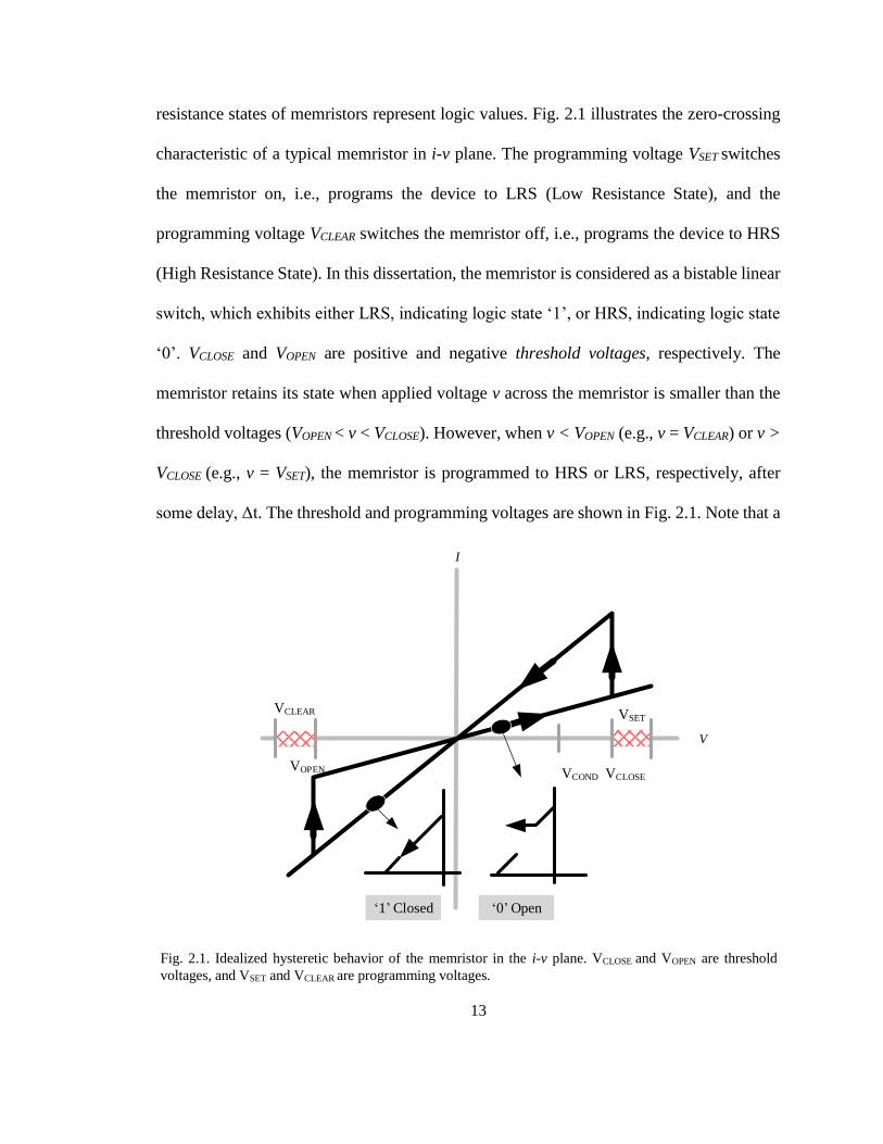
13
resistance states of memristors represent logic values. Fig. 2.1 illustrates the zero-crossing
characteristic of a typical memristor in i-v plane. The programming voltage VSET switches
the memristor on, i.e., programs the device to LRS (Low Resistance State), and the
programming voltage VCLEAR switches the memristor off, i.e., programs the device to HRS
(High Resistance State). In this dissertation, the memristor is considered as a bistable linear
switch, which exhibits either LRS, indicating logic state ‘1’, or HRS, indicating logic state
‘0’. VCLOSE and VOPEN are positive and negative threshold voltages, respectively. The
memristor retains its state when applied voltage v across the memristor is smaller than the
threshold voltages (VOPEN < v < VCLOSE). However, when v < VOPEN (e.g., v = VCLEAR) or v >
VCLOSE (e.g., v = VSET), the memristor is programmed to HRS or LRS, respectively, after
some delay, Δt. The threshold and programming voltages are shown in Fig. 2.1. Note that a
1 Closed 0 Open
VOPEN
VSETVCLEAR
VCLOSE
V
I
VCOND
Fig. 2.1. Idealized hysteretic behavior of the memristor in the i-v plane. VCLOSE and VOPEN are threshold
voltages, and VSET and VCLEAR are programming voltages.
14
programming voltage is any value within a particular range as shown in Fig. 2.1. Memristors
are compatible with CMOS technology [43], and logic computing with hybrid CMOS-
memristor circuits can be quite beneficial (see Chapter 5).
This chapter is organized in the following order. Section 2.1 describes a memristor-based
circuit architecture. Section 2.2 explores some stateful logic gates realized with typical
memristors. The same logic gates are realized with rectifying memristors, i.e., memristors
with diode-like behavior, as described in Section 2.3. In Section 2.4, the implementation of
multi-input multi-output stateful gates are explained, and in Section 2.5, IMPLY Stateful
Diagram (ISD) and its extension for logic synthesize is described. A generic two-
dimensional crossbar structure and its potential problems are discussed in Section 2.6 and
2.7. Section 2.8 concludes the chapter.
2.2 CROSSBAR ARCHITECTURE
Memristors are non-volatile computational memories. A single switch can only perform
primitive operations TRUE and FALSE. When the switch is open, the application of VSET
across the device closes the switch realizing logic operation TRUE. When the switch is
closed, the application of VCLEAR across the device opens the switch realizing logic operation
FALSE. However, a basic logic operation such as material implication (IMPLY) requires
two memristive switches [20]. Fig. 2.2 illustrates a one-dimensional programmable circuit
known as crossbar or crossbar array. In this array, two memristive switches P and Q are
electrically connected through the wire W, which is grounded through load resistor RG.
Inputs are the resistance states of P and Q, whereas the output is the new state of switch Q.
15
Stateful logic gates are performed by two operations, namely, READ and WRITE. These
operations are realized simultaneously. For example, in stateful IMPLY operation, the
READ operation is performed by applying VCOND to P, where 0V <VCOND <VCLOSE, and the
WRITE operation is performed by applying VPROG to Q, where VPROG = VSET. The READ
operation drives the wire W to either ≈ VCOND or to ≈ 0V, depending on the state of P. The
WRITE operation may toggle the state of Q, depending on the initial states of both P and
Q. The state of P remains unchanged during the operations.
Let LRS (also denoted by RCLOSED) represents logic ‘1’, and HRS (also denoted by ROPEN)
represents logic ‘0’. It is the case that ROPEN ≫ RCLOSED. Since the correct operation of the
circuit requires VW (the voltage on W) to be either ≈ 0V or ≈ VCOND, care must be taken to
ensure ROPEN / RG >> 1 and RG / RCLOSED >> 1. Assuming these inequalities are satisfied, RG
can be set as the geometric means of ROPEN and RCLOSED, i.e., RG = √ (ROPEN × RCLOSED).
A flow of current through Q could disturb the WRITE operation. If this current raises VW in
a time interval shorter than the switching time of Q, the WRITE operation will be disturbed.
Therefore, the RC delay of the circuit should be larger than the switching delay of memristor
Q. However, a large RC delay slows down the circuit operation. The use of external CMOS
circuitry—a keeper circuit— can help to improve the speed and accuracy of the circuit
operation [44]; however the area overhead would present another challenge.
A better way to suppress the current through Q would be to use the rectifying memristive
switches [15], [45], [46], elaborated in Section 2.3, with the circuit configuration of 0V
< VCOND < VCLOSE and VOPEN < VPROG < 0V. This circuit architecture suppresses the current
through Q during the WRITE operation and enables the converse nonimplication operation

16
(CNIMP), also known as inhibition operation (INH or INHIBIT), without additional CMOS
circuitry [25]. A two-input INH gate computes 𝑝 or 𝑞 where p and q are the inputs.
2.3 RECTIFYING MEMRISTORS
The rectifying memristors are resistive switches with intrinsic diode-like behavior with
a large resistive ratio of 3-6 orders of magnitude, e.g., 103 ≤ ROPEN/ RCLOSED ≤ 106 [15] and
[45-46]. The rectifying memristors suppress the current below 0.1 pA, when reverse biased
[45]. Memristors with a diode-like behavior can perform reliable logic operations without
any need for keeper circuits.
A crossbar array of rectifying memristors can be used to perform stateful INH operations
with voltage scheme 0V < VCOND < VCLOSE and VOPEN < VPROG < 0V. This voltage scheme
sets P forward biased and Q reverse biased and thus suppresses the current through the
target memristor, Q. As a result, VW remains unchanged ensuring that the WRITE operation
VCOND VPROG
RG
P Q
W
Fig. 2.2. Schematic diagram of a 1 × 2 crossbar array. The instant application of voltage pulses VCOND and
VPROG to switches P and Q, respectively, may toggle the logical state of Q depending on the initial state of P
and Q.

17
is performed correctly. This voltage configuration is used to perform stateful INH
operations without any need for keeper circuits, as elaborated in Section 2.5.
A simplified model for rectifying memristor is described by (2.1) and (2.2) [47]. In
Equation (2.1), R represents the resistance of the rectifying memristor; 𝑠 is the state variable
normalized between 0 and 1; 𝑣 is the applied voltage across the memristor; ROPEN represents
the resistance when the memristor is in HRS; RCLOSED represents the resistance when the
memristor is in LRS. For convenience, ROPEN is also used for reverse biased memristor.
The typical values of ROPEN and RCLOSED, which are shown in Table 2.1, are chosen based
on empirical results reported in [15]. The dynamic behavior of the state variable 𝑠 is
described by (2.2) where 𝑣𝐶𝐿𝑂𝑆𝐸 is a positive threshold voltage; 𝑣𝑂𝑃𝐸𝑁 is a negative
threshold voltage; VSET is a positive programming voltage; and VCLEAR is a negative
programming voltage. In addition, α is a positive constant related to the programming rate
of a memristor. In this dissertation, α is assumed to be 125 ×107 (Vs)-1 as used in [47].
𝑅 = 𝑅𝑂𝑃𝐸𝑁 (
𝑅𝐶𝐿𝑂𝑆𝐸𝐷
𝑅𝑂𝑃𝐸𝑁 )𝑠
𝑣 ≥ 0
𝑅𝑂𝑃𝐸𝑁 𝑣 < 0 (2.1)
𝑑𝑠
𝑑𝑡= 𝛼(𝑣 − 𝑣𝐶𝐿𝑂𝑆𝐸) 𝑣 ≥ 𝑣𝐶𝐿𝑂𝑆𝐸𝛼(𝑣 − 𝑣𝑂𝑃𝐸𝑁) 𝑣 ≤ 𝑣𝑂𝑃𝐸𝑁 0 𝑒𝑙𝑠𝑒𝑤ℎ𝑒𝑟𝑒
(2.2)
Table 2.1
Memristor’s spice model parameters [47]
Parameter Value
ROPEN 500MΩ
RCLOSED 500KΩ
𝒗𝑪𝑳𝑶𝑺𝑬 1V
𝒗𝑶𝑷𝑬𝑵 -1V
VSET 1.2V
VCLEAR -1.2V
α 125 × 107 (V. s)−1

18
With this value of α, the state transition in a memristor initially in HRS is 4 ns when the
applied voltage across the memristor is v = VSET. Comparable programming rates have been
reported in [40] and [42], as well. Substituting all related values in (2.2) results in
0.2 1.2
0.2 1.2
0
vds
vdt
elsewhere
and thus,
0.2 1.2
0.2 s 1.2
1.2 1.2
init
init
init
T s v
s T v
s v
where sinit and s+ are the initial and next states of the memristor, and T+ and T־ are the
switching delays (from HRS to LRS and from LRS to HRS, respectively). T+ and T־ are
assumed to be equal though, in general, they might be different. The solution for (2.2) is
1 1.2
0 1.2
1 1init
v
s v
s v
Fig. 2.3. Characteristics of a rectifying memristor. (Left) The i-v characteristic of rectifying memristor.
(Right) The s-v characteristic of rectifying memristor. The diagrams are depicted using the LTspice simulator
and the memristor model in [47].

19
Fig. 2.3 shows the i-v characteristic of a rectifying memristor. It also shows the s-v
characteristic of a memristor where s remains unchanged when vOPEN ≤ v ≤ vCLOSE. Table 2.1
shows the parameters of the memristor as used in [47]. The SPICE model used to plot
Fig. 2.3 is also explained in [47].
2.4 STATEFUL LOGIC GATES REALIZED WITH TYPICAL MEMRISTORS
Now that the basic circuit design concepts have been discussed, the question becomes
what types of stateful logic gates can be realized given specific design choices. In this
section, designs with typical memristors are discussed, and in Section 2.5 designs based on
rectifying memristors is discussed. All polarity combinations of VCOND and VPROG are applied
to a 1 × 2 crossbar array of typical memristors to examine what types of logic operations
can be realized by the circuit. The same procedure is applied to a 1 × 2 crossbar array of
rectifying memristors.
1) Stateful AND gate
The stateful AND gate was proposed in [23]. A 1 × 2 crossbar array alone is not sufficient
to implement the gate; a keeper circuit is required. The stateful AND gate requires VPROG <
VOPEN < VCOND < 0V and VOPEN < VPROG –VCOND. With this voltage combination, the use of a
keeper circuit is necessary. Without a keeper circuit, there is no logic operation, however,
with a keeper circuit, there is a logic AND operation. Take, for example, the case where P
and Q are both logic ‘0’, denoted as p, q = [0, 0] where p is the state of memristor P and q
is the state of memristor Q. The READ operation drives word line W to ≈ 0V. After the
WRITE operation, the voltage across Q is below VOPEN so Q remains ‘0’, as expected.
Similarly, when P is ‘1’ the crossbar array behaves as expected, regardless of the state of Q.
20
However, in the case where p, q = [0, 1], the crossbar array does not exhibit the desired
behavior. The READ operation drives W to ≈ 0V. Since RG >> RCLOSED of Q, the WRITE
operation drops VPROG across RG and thus the voltage difference across Q is approximately
0V. This is insufficient to change the state of Q. Therefore the AND function would operate
incorrectly. Laiho et al. [44] proposed splitting the simultaneous READ/WRITE operations
into consecutive operations. During the READ operation, the voltage drop on W is sampled
by the keeper circuit. During the WRITE operation, the keeper circuit forces the sampled
voltage onto W. Consequently, VPROG drops entirely across Q. That voltage drop is sufficient
to toggle the state of Q to ‘0’, which is the desired behavior of AND gate. The area overhead
of the keeper circuit is not the only obstacle that needs to be overcome; AND is not a
universal gate. In order to have a functionally complete set of operations, inverter is also
required. Inverter can be realized as a special case of the stateful IMP gate, explained below.
2) Stateful IMP gate
The stateful IMP gate was proposed in [19-20] and is defined as q+:= p→q = ¬p+q where
‘→’ is the IMP (short for IMPLY) gate, and q+ is the new value of q, which is the output of
the IMP gate. IMP gate can be implemented with a keeper circuit or without a keeper circuit
if sufficient capacitance on W is assumed. With a keeper circuit, the crossbar array runs at
full speed with the cost of increased area and power; in contrast, without a keeper circuit,
the crossbar array runs slow, but it consumes less area and power. The stateful IMP gate
requires 0V < VCOND < VCLOSE < VPROG, and VPROG – VCOND < VCLOSE. Take, for example, the
case where p, q= [0, 0]. The READ operation drives W to ≈ 0V. The WRITE operation
causes a voltage drop sufficient to toggle the state of Q, which is the expected behavior, as

21
shown in Table 2.2. The circuit operates similarly for all combinations of p, q. Implication
is functionally complete logic operation when coupled with the FALSE operation. Recall
that the FALSE operation is implemented by VPROG = VCLEAR.
3) Stateful OR gate
Much like IMP, the stateful OR gate can be implemented with or without a keeper circuit,
and the same power, speed, and area tradeoff applies. In practice, the use of a keeper circuit
in parallel with voltage divider ensures the correct operation of the circuit. The stateful OR
gate requires VOPEN < VCOND < 0V < VPROG < VCLOSE, and VCLOSE < VPROG –VCOND. With these
control voltages, the circuit operates correctly. OR is not a universal gate. In order to have
a functionally complete set of operations, inverter is also required.
4) Additional stateful gate
As discussed earlier in this section, different polarity combinations of VCOND and VPROG
implement different logic operations. There remains one voltage combination to consider:
VOPEN < VPROG < 0V < VCOND < VCLOSE, and VCOND – VPROG > VCLOSE. Assuming sufficient
capacitance on W, this polarity combination of control voltages implements the OR gate
with the output on P instead of Q. However, the use of a keeper in parallel with RG produces
the INH gate. The stateful INH gate was proposed in [25] and is defined as q+:= p↛q = ¬p∙q
where ‘↛’ is the INH gate. The truth table of INH logic is shown in Table 2.3. Take, for
example, the case where p, q= [1, 1]. The READ operation drives W to ≈ VCOND. During the
READ operation, the voltage on W is sampled by the keeper circuit. During the WRITE
operation, the keeper circuit forces the sampled voltage onto W. Consequently, the voltage
across Q becomes VPROG –VCOND. This voltage difference is sufficient to toggle the state of
Q to ‘0’, which is the desired behavior of the INH gate. Inhibition is functionally complete

22
logic operation when coupled with the TRUE operation. Recall that the TRUE operation is
implemented by VPROG =VSET. Similar to its use in the AND gate, the keeper circuit here
splits READ/WRITE into two consecutive operations.
In summary, a 1 × 2 crossbar array of typical memristors is sufficient to implement
several useful logic gates as long as care is taken in the selection of load resistor RG. Which
particular logic gate is implemented depends on the magnitude and polarity of the applied
Table 2.2
Truth table of the IMPLY operation
q+:= p→q = ¬p + q
In1 In2 Out
p q q+:= p⟶q
0 0 1
0 1 1
1 0 0
1 1 1
Table 2.3
Truth table of the INH operation
q+: p↛q = (¬p) q
In1 In2 Out
p q q+:= p↛q
0 0 0
0 1 1
1 0 0
1 1 0
Table 2.4
Logic gates realized by all possible voltage polarities and keeper/no-keeper circuit combinations
Polarity Logic Function
VCOND VPROG Sufficient capacitance on W With keeper circuit
+ + q+:= p→q q+:= p→q
- + q+:= OR (p, q) q+:= OR (p, q)
+ - p+:= OR (p, q) q+:= p↛q
- - No logic operation q+:= AND (p, q)
Signs + and – denote positive and negative voltage values of VCOND and VPROG defined for each logic
function in Section 2.4.

23
control voltages and on whether or not a keeper circuit is used. The circuit that provides
these control voltages is called a driver. Drivers are different than keeper circuits as
explained in Section 2.5 and 2.6. Keepers are auxiliary circuits required to perform reliable
operations. As already discussed, Table 2.4 summarizes the logic gates realized by all
possible voltage polarities and keeper/no-keeper circuit combinations. A 1 × 2 crossbar
array of typical memristors without a keeper circuit enables only IMPLY and OR logic
gates. When a keeper circuit is available, the memristors can realize all four operations:
AND, OR, IMP, and INH. Availability of more basic gates for synthesis allows for more
efficient realization of many Boolean functions, but also calls for invention of new logic
synthesis algorithms to synthesize arbitrary functions in new bases.
2.5 STATEFUL LOGIC GATES WITH RECTIFYING MEMRISTORS
This section explains which logic functions can be realized in a crossbar array of
rectifying memristors. The application of all polarity combinations of VCOND and VPROG
results in IMP and INH logic gates, as explained below. Table 2.5 summarizes the logic
gates realized by all voltage polarities and keeper/no-keeper circuit combinations.
1) Stateful IMP gate
A stateful IMP gate is realized with the same polarity combinations of VCOND and VPROG
described in a crossbar array with typical memristors, 0V < VCOND <VCLOSE < VPROG and
VPROG –VCOND < VCLOSE. An IMP gate can be implemented with a keeper circuit or without
a keeper circuit assuming sufficient capacitance on W. The same speed/power/area tradeoff
imposed by a keeper circuit in a crossbar array with typical memristors also holds for a
crossbar array with rectifying memristors.
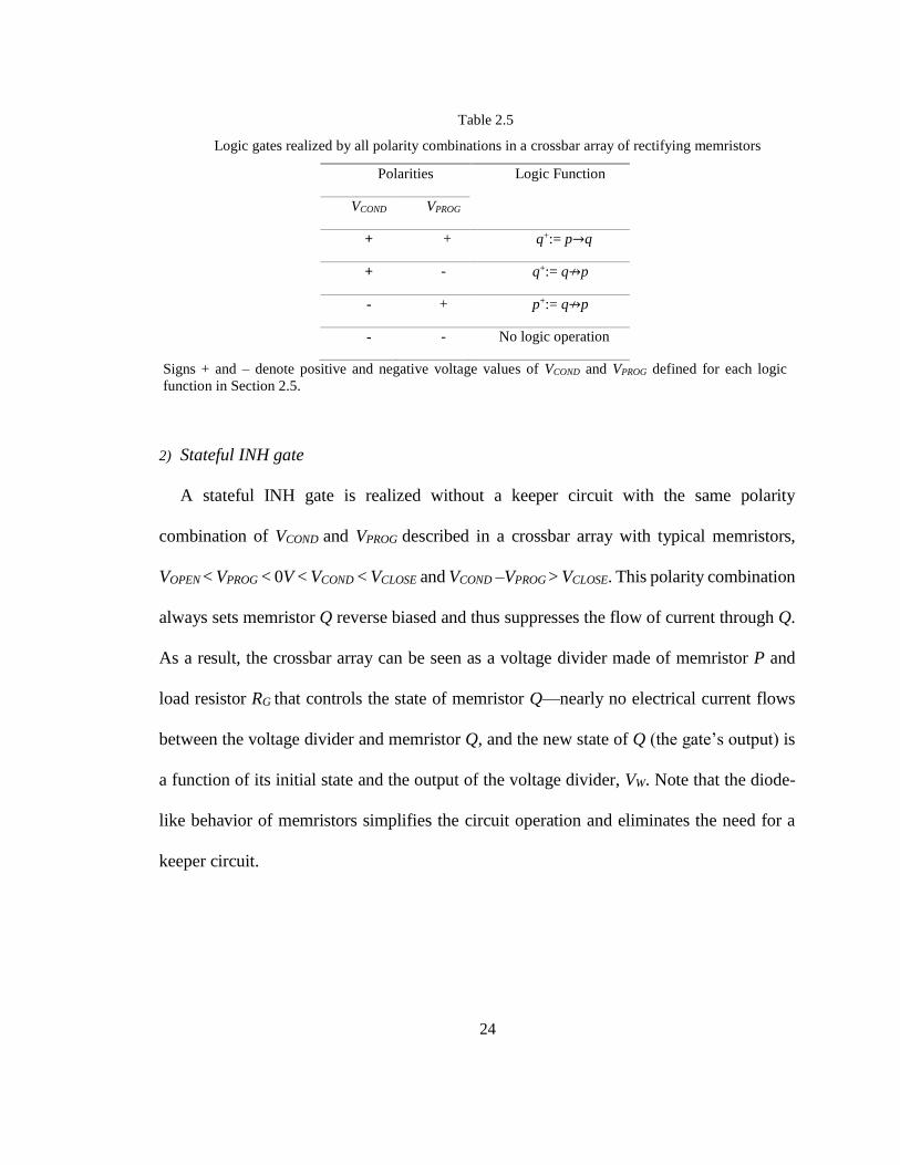
24
2) Stateful INH gate
A stateful INH gate is realized without a keeper circuit with the same polarity
combination of VCOND and VPROG described in a crossbar array with typical memristors,
VOPEN < VPROG < 0V < VCOND < VCLOSE and VCOND –VPROG > VCLOSE. This polarity combination
always sets memristor Q reverse biased and thus suppresses the flow of current through Q.
As a result, the crossbar array can be seen as a voltage divider made of memristor P and
load resistor RG that controls the state of memristor Q—nearly no electrical current flows
between the voltage divider and memristor Q, and the new state of Q (the gate’s output) is
a function of its initial state and the output of the voltage divider, VW. Note that the diode-
like behavior of memristors simplifies the circuit operation and eliminates the need for a
keeper circuit.
Table 2.5
Logic gates realized by all polarity combinations in a crossbar array of rectifying memristors
Polarities Logic Function
VCOND VPROG
+ + q+:= p→q
+ - q+:= q↛p
- + p+:= q↛p
- - No logic operation
Signs + and – denote positive and negative voltage values of VCOND and VPROG defined for each logic
function in Section 2.5.

25
The stateful INH gate can also be realized with the same polarity combination of VCOND
and VPROG described in a crossbar array with typical memristor for q+:= OR (p, q), i.e. VOPEN
< VCOND < 0V < VPROG < VCLOSE, and VCLOSE < VPROG –VCOND. This configuration implements
the INH gate with the output on P instead of Q. In other words, P is the target memristor
whereas Q is the source memristor. No keeper is required for this circuit configuration, as
well.
There remains one voltage combination to consider: VPROG < VOPEN <VCOND < 0V and
VOPEN < VPROG –VCOND. This circuit configuration produces no logic operation. Note that
stateful OR and AND gate cannot be realized with a crossbar array of rectifying memristors
without a keeper circuit. Fig. 2.4 illustrates a schematic diagram of a keeper circuit that
enables all stateful logic gates [48]. During the READ operation, source memristors are
driven with VCOND > 0V. During the WRITE operation, the keeper circuit forces 0V, VCOND,
Read
VCOND
VW
W
RG
Read
VPROG
VW- VW
Fig. 2.4. Schematic of a keeper circuit [Redrawn from 48]. VW denotes the voltage on W.

26
or - VCOND onto W depending on the result of READ operation and the type of stateful
operation. This keeper circuit can be used in a crossbar array with typical memristors and
rectifying memristors.
Table 2.6 summarizes the tradeoffs discussed in Section 2.4 and 2.5 for logic
implementations in a crossbar array with typical and rectifying memristors. Among all
design choices shown in Table 2.6, logic computations with rectifying memristors and
stateful INH gates require no keeper circuits. In addition, INH logic with TRUE operation
forms a complete set of logic gates. The use of rectifying memristors will also prevent the
disturbance of the WRITE operation, as discussed in Section 2.2. The simplicity and area
and power efficiency of the circuit are additional features of this particular design choice.
The use of rectifying memristors also enables multi-input multi-output INH gates without
additional CMOS circuitry, as discussed in Section 2.6. Rectifying memristors suppress
leakage currents, known as sneak current paths, as explained in Section 2.8. The sneak
current is an undesired phenomenon, which occurs in two-dimensional crossbar arrays, and
it may disturb the READ and WRITE operations. We rely on rectifying memristors for logic
computing for the all benefits mentioned above.
Table 2.6
Tradeoffs for logic implementations in a crossbar array of typical and rectifying memristors
Crossbar array with Typical memristors Rectifying memristors
Logic operation AND IMP OR INH IMP INH
Complete logic set No with
FALSE No
with TRUE
with FALSE
with TRUE
Keeper Yes No
Area/ power / complexity Potentially high Potentially low
Sneak current paths Larger Smaller

27
In summary, realization of stateful logic gates in one dimensional crossbar array of
typical memristors and rectifying memristors are explained. The conditions for the
correctness of the circuit operations are also studied.
2.6 MULTI-INPUT MULTI-OUTPUT INH GATE
A multi-input multi-output INH gate can be realized in a 1 × n crossbar array of
rectifying memristors. Fig. 2.5 shows a 1 × 9 crossbar array for computing function
, , , , ,F OR a b c d OR a b c e where M1-M5 are used as source memristors
whose logical states represent input variables a, b, c, d, and e; memristors M6 and M7 are
auxiliary memristors, which store intermediate signals; and M8 and M9 are target
memristors, which store the outputs, . , .a b c d a b c e . Function F is
realized in three steps as described below.
1) FALSE operation: Reset the memristors to HRS by connecting the vertical wires to
VPROG < 0V, and the horizontal wire to VCOND > 0V. This step is realized in one clock
cycle.
2) Copy operation: Connect the input voltages to the vertical wires of the source
memristors and VPROG to the horizontal wire to program (or copy the inputs into) the
source memristors. At the same time, connect the vertical wires driving the auxiliary
and target memristors to VCOND to set them to LRS. This step is realized in one clock
cycles, as well.
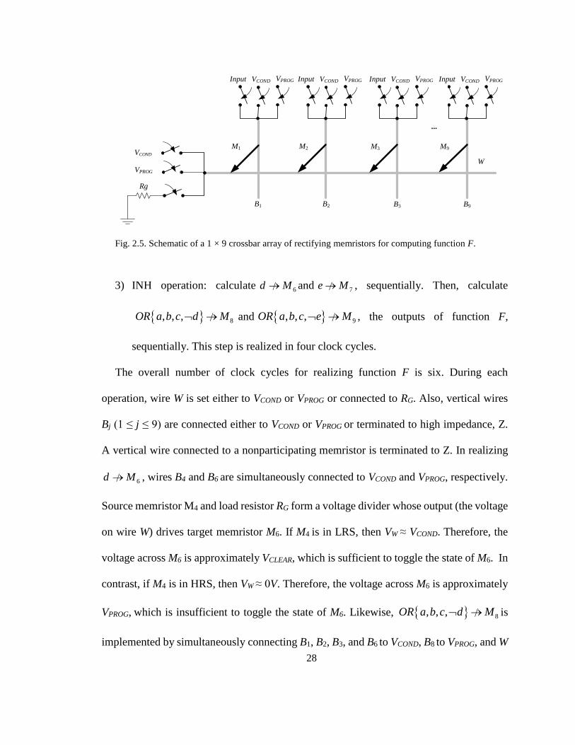
28
3) INH operation: calculate 6d M and 7e M , sequentially. Then, calculate
8, , ,OR a b c d M and 9, , ,OR a b c e M , the outputs of function F,
sequentially. This step is realized in four clock cycles.
The overall number of clock cycles for realizing function F is six. During each
operation, wire W is set either to VCOND or VPROG or connected to RG. Also, vertical wires
Bj (1 ≤ j ≤ 9) are connected either to VCOND or VPROG or terminated to high impedance, Z.
A vertical wire connected to a nonparticipating memristor is terminated to Z. In realizing
6d M , wires B4 and B6 are simultaneously connected to VCOND and VPROG, respectively.
Source memristor M4 and load resistor RG form a voltage divider whose output (the voltage
on wire W) drives target memristor M6. If M4 is in LRS, then VW ≈ VCOND. Therefore, the
voltage across M6 is approximately VCLEAR, which is sufficient to toggle the state of M6. In
contrast, if M4 is in HRS, then VW ≈ 0V. Therefore, the voltage across M6 is approximately
VPROG, which is insufficient to toggle the state of M6. Likewise, 8, , ,OR a b c d M is
implemented by simultaneously connecting B1, B2, B3, and B6 to VCOND, B8 to VPROG, and W
M1 M2 M9
Rg
...
VPROG
VCOND
W
B1 B2
M3
B3 B9
VPROGVCONDInputVPROGVCONDInput VPROGVCONDInput VPROGVCONDInput
Fig. 2.5. Schematic of a 1 × 9 crossbar array of rectifying memristors for computing function F.
29
to RG. Alternatively, 8, , ,OR a b c d M can be calculated by implementing a sequence
of INH gates, i.e., 8a M ,8b M , and
8d M . A stateful INH gate can be used to
produce NOT and NOR gates as 1p p and ( , ) 1 ( , )OR p q NOR a b , which
requires programming the target memristors to logic ‘1’. Therefore, an arbitrary logic
function can be realized based on logic NOR.
Fig. 2.6 shows the schematic of memristive circuit proposed in this dissertation for
calculating logic functions in a crossbar array. The circuit consists of crossbar memory
array and crossbar computational array. The memory array stores the instructions and
control signals whereas the computational array executes logic operations and stores the
results. These crossbar arrays are connected through datapath. This circuit architecture
enables in-memory computing as the computational array calculates logic functions and
stores the outputs. The computational array are connected to CMOS drivers. The schematic
of each driver is shown in Fig. 2.7. The drivers can connect the wires to 0V, VCOND, VPROG,
or the Ground (GND) through RG. The circuit can realize any logic function with INH and
TRUE operations without any keeper circuit. The crossbar memory array is driven by
shifter. The output of the shifter in the first, second, and nth clock cycles are (v1, v2… vn) =
(1, 0 … 0), (0, 1, 0 … 0), and (0…0, 1), respectively. Each column of the crossbar memory
array stores the control signals required to perform one logical operation. The size of the
crossbar memory array depends on the number of horizontal and vertical wires of the
computational array, the number of logical operations (which is equal to the number of
clock cycles) and the driver’s control signals. Hence, its size can be written as (3×l) * n
where 3 is the driver’s signals, l is the sum of horizontal and vertical wires, and n is the

30
number of clock cycles. The size of the memory array dominates the area when large
circuits are implemented. The computational delay depends on a synthesis approach for
logic computations [49]. The power dissipations in memristive arrays are discussed in
Chapter 3, 5, 6, and 7.
In summary, stateful NOR gates is built from INH gates. A multi-input stateful NOR
gate is realized either sequentially by cascading stateful INH gates or simultaneously by
implementing all stateful INH gates in parallel. A multi-output stateful NOR gate can be
realized by simultaneously driving several target memristors to VPROG.
3
Crossbar Memory Array
Shifter
. . . . . .
Computational Array
Driver Circuitry
3
3
3
3
3
v1
v2
vk
v(n-1)
vn
. . . . . .
Fig. 2.6. Schematic of memristive computing circuit including control and datapath units.

31
2.7 EISD: EXTENDED IMP SEQUENTIAL DIAGRAM
The IMP Sequential Diagram (ISD) [49] is used for analysis and synthesis of stateful
logic circuits. In this notation, each horizontal wire represents the state of a memristor over
the course of synthesis. Fig. 2.8 shows the symbolic diagram of the IMP gate where p and
q are inverting and non-inverting inputs of the IMP gate, stored in source and target
memristors P and Q, respectively. The output of IMP gate is the new state of Q, which is
p q .
Via between CMOS and nanowire
0V VCOND
VPROG RG
Fig. 2.7. (Left) Schematic of a computational array connected to CMOS drivers. (Right) Schematic of
each driver circuitry.
P p
Q q p IMP q = ¬ p+q+
p
Fig. 2.8. Symbolic diagram of a 2-input IMP gate in ISD notation.

32
Fig. 2.9 shows the ISD notation of NAND (p, q). The gate is implemented in three clock
cycles. In the first clock cycle, the FALSE operation programs memristor R to HRS, i.e.,
r = 0; the symbolic diagram of the FALSE operation is shown as a rectangle with label ‘0’.
In the second and third clock cycles, p r and q r are implemented. The new values
of r over the course of operations are shown alongside wire R. There is no more operations
defined in ISD, as IMP and FALSE form a complete set of logic gates. In this dissertation,
the ISD notation is extended (Extended ISD or EISD) to include INH and TRUE
operations, as well. Fig. 2.10 shows the symbolic diagram of the INH gate where p and q
are inverting and non-inverting inputs, stored in source and target memristors P and Q,
respectively. The output of the gate is the new state of Q, which is pq .
P p
q
¬p+(¬q)= ¬ (p+q)R r +0
0
+¬ p
p
Q q
Fig. 2.9. ISD of function NAND (p, q) where the output is stored as a new state of memristor R.
P p
Q q ¬ pq×
p
Fig. 2.10. Symbolic diagram of a two-input INH gate in EISD notation.

33
Fig. 2.11 shows the EISD notation of function ,OR p q r . This function is performed
in two clock cycles. In the first clock cycle, the TRUE operation sets memristor R to
logic ‘1’. The symbolic diagram of the TRUE operation is shown as a rectangle with label
‘1’. In the second clock cycle, the INH operation is performed. The new values of r over
the course of synthesis are shown alongside wire R. Memristors P, Q, and R in Fig. 2.11
are rectifying memristors, hence enabling stateful INH gate with multiple fan-out without
P p
Q q
¬ (p+q)R r
× 1
1
p
q
P p
Q q
¬ (p+q)R r × 1
1
p
q
Fig. 2.11. EISD of NOR gate. Different EISD notations for r = NOR (p, q) depending on source and
target memristors locations.
P p
Q q
¬ (p+q)R r × 1
1
¬ (p+q)S s × 1
1
Fig. 2.12. EISD of multi-output function , , ,OR p q r OR p q s .
p
q
1
1×
× ×
×
1
1
׬ p
p ¬qp
¬pq
XNOR (p, q)
× XOR (p, q)
T1-T2 T3 T4 T5 T6 T7 T8 T9
Fig. 2.13. EISD of ( , ) 1 1XOR p q p q q p .

34
a keeper circuit. Fig. 2.11 shows two different EISD notations for ,OR p q r as
different source and target memristors are chosen in each diagram for synthesizing the
function. Fig. 2.12 shows the EISD of multi-output function
, , ,OR p q r OR p q s . Fig. 2.13 shows the EISD of function
( , ) 1 1XOR p q p q q p . The diagram also shows the timing aspect
of the circuit, e.g., at T4 (the fourth clock cycle) value p is copied into the bottom most
memristor (wire). In the course of synthesis, it is not possible to READ from and WRITE
to a memristor simultaneously. For example, the instant implementation of p q and
q p requires reading from and writing to memristor P, hence, a copy of value p is stored
in an auxiliary memristor to avid the issue. The synthesis delay is nine clock cycles. This
XOR p XNOR q
1
1 XOR
XOR (p, q, r)
1
1 r
p
q
1
1 1
(a)
XOR p XNOR q
1
1
XOR
XOR (p, q, r)
1
1
p
q
1
1
1
WRr
(b)
Fig. 2.14. EISD notation of XOR (p, q, r). (a) The XOR gate is implemented with 15 operations and five
memristors. (b) The XOR gate is implemented with 16 operations and four memristors. The EISD shows
the trade-off between the number of memristors and the operations.

35
delay includes that of initialization and programming step. The overall number of
memristors used in this implementation is four. In EISD notation, gates and sub-circuits
are shown by blocks to simplify the diagram. For example, Fig. 2.14 shows the EISD
notation of a 3-input XOR gate realized as a cascade of 2-input XOR gates. Each XOR
gate consists of a number of INH and TRUE operations, as shown in Fig. 2.13. The 3-input
XOR (p, q, r) is implemented with five memristors in 15 clock cycles (Fig. 2.14a).
The EISD notation shows the tradeoff between the number of memristors and the
number of stateful gates. For example, the 3-input XOR gate can also be realized in 16
clock cycles and four memristors, i.e., by writing input r into the memristor P after
calculating p XNOR q, as shown in Fig. 2.12b. The rectangle with label WR indicates
writing input r into memristor P. Note that the WRITE operation is performed by
connecting one terminal of the memristor to input r and the other terminal to VPROG.
In summary, ISD is a notation used for analyzing and synthesizing stateful circuits and
shows the tradeoff between the number of memristors and the number of clock cycles
(logic operations). The proposed EISD generalizes the ISD notation.
2.8 TWO-DIMENSIONAL CROSSBAR ARRAY
Two-dimensional self-aligned crossbar arrays are regular structures with very high
density. Fig. 2.15 shows a 3 × 3 memristor crossbar array. At each junction, an area between
two perpendicular wires, one memristor is located. Each wire of the crossbar array is
connected to a CMOS driver, and each memristor is uniquely accessible. A stack of crossbar
arrays formed on CMOS layers creates a three-dimensional memristive array. CMOL
(CMOS-MOLECULE SCALE DEVICE) [20] is one example of 3D memristive arrays. The

36
primary use of the 3D arrays (three-dimensional crossbar arrays) is for memory
applications. In this dissertation, the focus is mainly on logic calculations in two-
dimensional crossbar arrays, or simply crossbar arrays.
Despite the simplicity, regularity, and high density of the crossbar arrays, there are some
potential problems such as half-select problem and sneak current paths limiting the size of
these arrays and disturbing their operations. For example, suppose that the crossbar array,
shown in Fig. 2.15 consists of non-rectifying memristors. Programming the upper right
corner memristor to LRS requires driving the right-most vertical wire to VSET and the
uppermost horizontal wire to 0V. This configuration half-selects the right-most column
memristors, i.e., only one terminal of each half-select memristor is driven by VSET while the
other terminal is floated (terminated to Z) [50]. Similarly, the uppermost row memristors
connected to 0V are half-selected, as well. The half-select memristors may cause sneak path
problem. The sneak path, as shown by a red-dash lines in Fig. 2.16, may inadvertently toggle
the state of a memristor or disturb the READ and WRITE operations. For example,
memristor M is intended for measuring the response. A current path through memristors
other than memristor M is a sneak path current. Fig. 2. 16 shows the dominant sneak path
current, which follows through half-select memristors in LRS.

37
RCLOSED
ROPEN
VSET
0V
Z
Z
Half-Select Memristors
ZZ
Fig. 2.15. A 3×3 crossbar array of non-rectifying memristors.
Fig. 2.16. Half-select problem may cause sneak current paths. The green dash-line represents the desired
current path whereas the red dash-lined represents an undesired sneak current path.
Z
Z
VTRUEZZ
M
RG Z
Z
VPROGZVCOND
P Q
RG
VPROGVCOND
3RCLOSEDP Q
(a) (b)
Fig. 2.17. (a) The sneak path disturbs the READ and WRITE operations. (b) The circuit equivalent of
the crossbar array with sneak current path.

38
Fig. 2.17a shows how a sneak path disturbs the READ and WRITE operation. Suppose
that the upper left corner memristor P is driven by VCOND and the upper right corner
memristor Q is driven by VPROG implementing :q p q . This operation falsely results
in q = 0 due to the sneak path problem. The green dash-line in Fig. 2.17a illustrates the
desired current path through memristor P whereas the red dash-line represents an undesired
sneak current path. The sneak path disturbs the READ operation since it adds up a parallel
resistance to memristor P, hence increasing the voltage on the uppermost wire. This voltage
increase disturbs the WRITE operation, as well, since it decreases the voltage difference
across memristor Q and makes it insufficient to toggle the state of Q. Fig. 2.17b shows the
circuit equivalence to the crossbar array while implementing :q p q . Note that the
sneak path crosses through the reverse biased LRS memristors, as shown in Fig. 2.17b.
The sneak current paths can be suppressed by connected the crossbar wires to proper
voltage values. For example, Fig. 2.18a shows a voltage scheme for a reliable READ
operation. In this scheme, the left-most vertical wire is set to VCOND while other vertical
wires of the crossbar array are grounded. The current through memristor P is fed to a sense
amplifier, which acts as a current-to-voltage converter. The output of the amplifier
determines the state of memristor P. This voltage scheme suppresses the sneak paths and
enables a reliable READ operation. However, this voltage scheme may cause a power
dissipation in other left-most column memristors depending on their resistance states.
Fig. 2.18b shows another voltage scheme for a reliable WRITE operation [51]. In this
scheme, the vertical and horizontal wires connected to memristor P are set to VSET and 0V,
respectively, while other crossbar wires are connected to VSET/2. This biasing scheme limits

39
the sneak paths and enables a reliable WRITE operation. However, this scheme may also
cause a power dissipation in other left-most column memristors of the crossbar array. There
are other techniques that can be used to improve the READ and WRITE operations as
studied in [51-53]. The use of rectifying memristors is our design choice to limit the sneak
paths in crossbar arrays. Rectifying memristors limits reverse biased currents, which cause
the sneak path currents, below 10–13 A. Studies show that the diode-like behavior of the
rectifying memristors effectively improves the read operation performance of a large scale
crossbar memory array without cell-selectors [54].
In addition to the sneak current paths, a nonzero resistance of wires could be another
challenge for reliable READ and WRITE operations [55-56]. This resistance degrades the
voltage along the wires and causes unequal voltage drops across the memristors. When all
memristors on a selected column are at LRS, the farthest memristor from the driver is the
0V
0V
P
VCOND 0V 0V
0V
VSET/2
VSET/2
P
VSET VSET/2 VSET/2
0V
(a) (b)
Fig. 2.18. Biasing schemes for READ and WRITE operation. These schemes limit the sneak path currents.

40
worst-case selected memristor, which sees the largest voltage degradation during the
WRITE operation (Fig. 2.19). The fidelity of the READ operation depends on the state of a
selected memristor as well as the states of other memristors in the crossbar array. The worst
performance of the READ and WRITE operations occurs under following circuit
circumstances [55]: 1) when a selected memristor is in LRS, other memristors of a selected
column are in HRS, and other crossbar memristors are in LRS, the READ operation has the
worst performance, and 2) when a selected memristor is in HRS while other memristors of
the crossbar array are in LRS, the READ and WRITE operation have the worst performance.
The maximum size of a crossbar array is determined based on the worst READ and WRITE
performance of memristors. To maximize the size of a crossbar array, the power
consumption should be minimized. This can be done by increasing the resistive values of
RCLOSED and ROPEN while keeping the ROPEN/RCLOSED ratio sufficiently large, as suggested in
The farthest
memristor from the
driver
Symbolic
drivers
...
...
...
...
...
.
.
.
Fig. 2.19. The effect of nonzero resistance of wires on the READ and WRITE operations.

41
[55]. However, this solution may increase the RC delay during a READ and WRITE
operation. In contrast to the previous works [55-56], recently, Youn et al. showed different
examples of the worst read scenarios in the crossbar arrays [57].
Fig. 2.20 shows the schematic of the memristor circuit proposed in this dissertation for
computing logic functions in a two-dimensional array. A driver circuit connected to each
wire of the crossbar array is shown in Fig. 2.7. These drivers enable row and column
operations in the computational crossbar array [47] and [74]. The complexity and
computational delay (measured as the number of clock cycles) of the circuit are related to
logic synthesis approaches used to realize functions. The size of the crossbar memory array
depends on the size of the computational array, the number of control signals used for
3
Crossbar Memory Array
Shifter
. . .
. . .
Computational
Array
Driver
Circuitry
3
3
3
3
v1
v2
vk
v(n-1)
vn
3
. . .
. . .
3
. . .
3
Fig. 2.20. Schematic of the complete memristor crossbar array. The driver circuitries are illustrated in
Fig. 2.7.
42
driving each wire of the computational crossbar array, and the size of the circuit realized in
computational array. See Chapter 3, 5, 6, and 7 for power analysis of memristor circuits.
In summary, the limitations of the cross array and the potential solutions are discussed.
In addition, a new general memristor circuit structure for logic computing in two-
dimensional array is proposed.
2.9 LOGIC COMPUTATIONS IN A CROSSBAR ARRAY
This section explains how to calculate logic functions in a crossbar array of rectifying
memristors with INH and TRUE gates. An implementation of 3-input XOR gate in the Sum-
of-Products (SOP) form, i.e., ( , , )XOR p q r pqr pqr pqr pq r is explained in the
following three steps.
1) Initialization: This step sets the memristors to logic ‘1’. Setting the memristors with
random states to logic ‘1’ may increase the power dissipation in the crossbar array.
Instead, if the memristors were logic ‘0’, their programming to logic ‘1’ would
decrease the power dissipation. Furthermore, programming the memristors to logic
‘0’ requires small amounts of power as memristors are set reversely biased. Therefore,
this step is realized with two consecutive FALSE and TRUE operations in two clock
cycles. The entries of the symbolic matrix, shown in Fig. 2.21 represent the logic
values stored in each memristor of the crossbar. The label on top of the arrow indicates
the number of operations required for the initialization.

43
2) Mapping: This step shows how to map the XOR gate into the crossbar memristors.
Suppose that the bottommost row memristors of the crossbar array store inputs p, q,
and r (Fig. 2.22a). The columns of the crossbar array are programmed one by one
using multi-output INH gates. For example, the left-most column memristors of the
crossbar array are programmed using two consecutive INH gates31 41( , )p m m and
31 11 21( , )m m m where mij shows the state of a memristor at intersection row i and
column j. The results of the inhibition operations are shown in Fig. 2.22b and 2.22c.
Similarly, other columns are programmed as shown in Fig. 2.22d. The total number
1 1 1 1
1 1 1 12
1 1 1 1
1 1 1 1
1p q r
1 1 1 1
1 1 1 11
1 1 1
1 1 1
1
p
p
p q r
1 1 1
1 1 11
1 1 1
1 1 1
1
p
p
p
p
p q r
1
14
1
1
1
p q r
p q r
p q r
p q r
p q r
(a) (b) (c) (d)
1
1
p q r pqr
p q r pqr
p q r pqr
p q r pq r
p q r
2
0 0 0
p q r pqr
p q r pqr
p q r pqr
p q r pq r
p q r XNR
XOR
(e) (f)
Fig. 2.22. Symbolic matrices illustrate the steps of computing XOR (p, q, r) with INH gates. The
number of operations (clock cycles) to implement the XOR gate is 11.
1 1 1 1
1 1 1 12
1 1 1 1
1 1 1 1
1 1 1 1
Fig. 2.21. Symbolic matrix. The entities show the values of the crossbar memristors.

44
of clock cycles for programming the columns is twice of the number of inputs, which
is six.
3) Calculation: This step explains how to calculate the XOR gate in the SOP form. First,
the products (minterms) are implemented with four multi-input INH gates
1,( ) 1, ( ) 1p q r p q r p q r , and ( ) 1p q r where each INH
gate is applied to one row of the crossbar array. The products are simultaneously
calculated and stored in the right-most column memristors as shown in Fig. 2.22e.
Next operation is to sum the products by two consecutive INH gates as
(( ) 1) 1pqr pqr pqr pq r . The first INH gate calculates logical NOR of
the products, which is equivalent to the logical XNOR of the inputs, and the second
INH gate inverts the output of the first INH gate producing XOR (p, q, r). Fig, 2.22f
shows the outputs of the INH gates.
The synthesis approach used for the XOR gate is similar to that proposed in [25] except
that cited approach [25] uses a combination of INH and IMP gates for synthesis. This
combination of logic gates decreases the delay but increase the complexity. There are two
types of operations, known as row and column operations, realized in crossbar arrays. Row
operations are applied to row memristors and column operations to column memristors. For
example, in step 3, the products (minterms) are implemented with row operations and the
sum (OR gate) with column operations. The INH gates used in row operations are realized
with VCOND > 0V and VPROG < 0V. However, opposite polarity of VCOND and VPROG is required
for implementing the INH gates in column operations.

45
One disadvantage of stateful logic computations is that stateful operations are
sequential, hence a long sequence of operations are required to perform a logic function.
With alternative circuit approaches, proposed in Chapter 3 and 4, a 3-inupt XOR gate can
be implemented with only three clock cycles as described in Chapter 5.
In summary, a 3-input XOR gate is implemented in a crossbar array of rectifying
memristors with multiple INH gates. The size of the crossbar array is 6 × 4 and the total
number of clock cycles is 11.
2.10 SUMMARY
This chapter explained the basic memristor crossbar structure. The sneak path problem
and some solutions were discussed. In addition, EISD notation was explained. Multiple
design choices for stateful logic circuits were reviewed. Rectifying memristors are
desirable for logic computations due to power and area saving benefits. This chapter also
described a new general circuit structure which enables in-memory computing.

46
Chapter 3
Memristive Volistor Logic Gates
This chapter introduces a novel volistor logic gate [29], which uses voltage as input and
resistance as output. Volistors rely on the diode-like behavior of rectifying memristors.
This chapter shows how to realize the first logic level, counted from the input, of any
Boolean function with volistor gates in a memristor crossbar network. Unlike stateful logic,
there is no need to store the inputs as resistance, and computation is performed directly.
The fan-in and fan-out of volistor gates are large and different from traditional memristor
circuits. Compared to a solely memristive stateful logic, a combination of volistors and
stateful inhibition gates can significantly reduce the number of operations required to
calculate arbitrary multi-output Boolean functions. The power consumption of volistor
logic is computed and compared with the power consumption of stateful logic using
simulation results—when implemented in a 1 × 8 or an 8 × 1 crossbar array, volistors
consume significantly less power.
3.1 INTRODUCTION
The stateful logic computations with memristors is an area of active research. Borghetti
et al. [20] proposed realizing the stateful logic via material implication (IMP). In classical
memristive stateful circuits, logic signals utilize resistance on input and output. In other
words, the previous resistance state of a memristor affects the operations. In contrast,
volistors do not use the previous resistance state in calculations. Other stateful logic gates
have been proposed as well, e.g., INH, AND, etc. In stateful logic, values are encoded by
resistance states of memristors. The stateful logic is usually performed in a generic crossbar

47
array. One key disadvantage of stateful logic is that a long sequence of operations is
required to implement an arbitrary Boolean function.
This chapter introduces a new concept in memristor logic, call volistor logic. Unlike a
stateful logic gate, a volistor (voltage-resistor) gate has voltage-based input and resistance-
based output. Therefore, volistors (volistor gates) can be used for first (possibly complex)
level of logic implementation. It is always assumed that negated inputs are available as
voltage signals. Volistors are implemented in generic crossbar arrays of rectifying
memristors. Logic synthesis methods with volistors are different from classical logic
synthesis. Multi-input multi-output volistor gates, implemented in a 1 × 8 crossbar array,
dissipate less power than corresponding stateful logic gates. The output of a volistor gate
is stored as a resistance state of a target memristor. The correct functionality requires
initializing the target memristor to LRS. With different coding schemes, either a volistor
OR and NAND logic set or a volistor NOR and AND logic set can be realized in the same
crossbar array. For instance, if the closed state of a memristor encodes logic ‘0’ and the
open state of a memristor encodes logic ‘1’, the set of OR and NAND operations is
implemented. The reverse encoding scheme implements the NOR and AND logic set. With
volistor logic, crossbar drivers need to supply only three voltage levels ,v v and 0V. In
addition, the drivers must be capable of connecting arbitrary wires in the crossbar to either
high impedance (Z) or grounding these wires through load resistors RG. Clearly, volistor
logic cannot implement arbitrary logical structures such as SOP, i.e., the volistor network
layer cannot implement every Boolean function. However, a combination of a volistor

48
NOR and AND with stateful INH, or their dual logic of volistor OR and NAND with
stateful IMP, can both be used to realize arbitrary multi-output Boolean functions.
This chapter is organized as follows. In Section 3.2, volistor gates are introduced. In
Section 3.3, the synthesis of arbitrary Boolean functions is explained. In Section 3.4, the
power consumption of volistor gates is computed and compared with stateful logic.
Section 3.5 is a summary and conclusion of the chapter.
3.2 VOLISTOR LOGIC
In this section, volistor logic is introduced. The key idea behind volistor logic is that
inputs are voltages and outputs are resistances. This is a significant change from the way
the voltage drivers are used in stateful logic; however, the target memristor is still used as
a memory element where the output is stored. The basic volistor logic gates are: inverter,
n-input NOR, and n-input AND, and their duals inverter, n-input OR, and n-input NAND.
The following subsections describe the basic architecture required for logic computations
and the basic logic gates.
3.2.1 Crossbar Structure
The basic circuit structures for volistor logic computations are the 1 × 2 crossbar array
and 2 × 1 crossbar array depicted in Fig. 3.1. Just as in stateful IMP, S denotes the source
memristor and T the target memristor. The wire B1 connected to source memristor S
conveys input signal VS. Let v+ = 0.6 V and v0.6– = ־ V. The logical coding scheme for VS
is defined as follows: v+ encodes logic ‘1’ denoted vs = 1, and 0V encodes logic ‘0’ denoted
49
vs = 0. The wire B2 connected to target memristor T carries a bias voltage, VT = v־.
Memristor T acts as a switch whose resistance state t represents the output of the crossbar
array. When T is open, its high-resistivity state encodes logic ‘0’, i.e. t = 0. When T is
closed, its low-resistivity state encodes logic ‘1’, t = 1. This interpretation of the resistivity
state of T is used for performing the NOR/AND logic set; another interpretation is
discussed in Section 3.2.5. Prior to logic computation, both memristors S and T must be
closed. To unconditionally close a memristor, it must be forward biased by VSET. The 1
× 2 crossbar array must satisfy (3.1). In particular, VT is selected such that VT-VS equals
VCLEAR when VS = v+.
0OPEN T
T S CLEAR
V V V
V V V
(3.1)
Each wire must be either driven by one of the voltages v+, 0, and VT, or terminated with
high impedance Z or grounded by load resistor RG. All these connections are realized with
B1 B2
W
VS VT
S T
W
VS
VT
B1
B2
S
T
Increase of
resistance
i
(a) (b)
Fig. 3.1. Crossbar arrays. (a) 1 × 2 crossbar array. (b) 2 × 1 crossbar array. The inset shows the symbolic
diagram of a memristor. The flow of current into the device, as shown above, increases the resistance.

50
CMOS switches shown symbolically in Fig. 3.2. RG is defined as geometric mean of
RCLOSED and ROPEN, i.e., √ (RCLOSED × ROPEN) = 15MΩ. The crossbar array operates by the
simultaneous application of VS and VT to S and T, respectively. Since VS > VT, current must
flow through the memristors. However, the application of these voltages forward biases S
and reverse biases T, thus suppressing the flow of current. This means that VW ≈ VS where
VW is the voltage on wire W. If Vs = v+, the voltage across T will toggle that memristor, i.e.,
the new state of target memristor T becomes t = 0.
The other basic structure for volistor logic is 2 × 1 crossbar array depicted in Fig 3.1b.
In this crossbar array, the logical coding scheme for VS is defined as follows: v־ encodes
logic ‘1’ denoted vs = 1, and 0V encodes logic ‘0’ denoted vs = 0. The 2 × 1 crossbar array
must satisfy (3.2). In particular, VT is selected such that S T CLEARV V V whenSV v .
0 T CLOSE
S T CLEAR
V V V
V V V
(3.2)
The crossbar arrays shown in Fig. 3.1 can be scaled to 1 × n and n × 1 arrays, allowing
for multi-input multi-output volistor logic gates. The 1 × n and n × 1 crossbar arrays must
Z
RG
VS
VT Wire
Fig. 3.2. Symbolic illustration of a driver circuit connected to each wire.

51
satisfy (3.1) and (3.2), respectively. These arrays implement wired-OR function where the
voltage on wire W denotes logical OR of inputs.
3.2.2 Volistor NOT gate in a one-dimensional array
An inverter is the simplest gate to realize in volistor logic; the symbolic diagram is
shown in Fig. 3.3a. Take, for example, the case where (vs, t) = (1, 1), i.e., vs = 1 and t = 1.
Both source and target memristors are initially closed. Volistor NOT can be realized in
either a 1 × 2 or 2 × 1 crossbar array. When realized in a 1 × 2 array, VT must be a negative
voltage, VS must be greater than or equal to 0V, per (3.2), and horizontal wire W must be
connected to high impedance Z. Setting W to Z allows VS to manifest on W. Based on
Ohm’s law, current should flow through the array, since VS -VT > 0V. However, memristor
T is reverse biased and thus suppresses the flow of current. In this case, the voltage drop
across S is 1.2 mV, i.e., the voltage on W equals 599 mV. The voltage drop across T is -
1.198 V, which is sufficient to open memristor T. This is the desired behavior of the inverter
V RVIN ROUT
V
VR ROUT
VIN1
VIN2
V
VR ROUT
VIN1
VIN2
V
RR ROUT
VIN
RIN
(a) (b) (c)
(d)
Fig. 3.3. Symbolic notations for volistor logic gates. (a) Volistor NOT. (b) two-input volistor NOR gate. (c)
two-input volistor AND gate. (d) mixed-input NOR gate. Inside the gates, symbols V and R denote whether
a signal is a voltage-based or resistance-based, respectively.

52
W
VS VT
S T
Z VT
X T
VT Z
T X
VT Z
T X
(a)
(b) (c) (d) (e)
Fig. 3.4. Behavior of volistor NOT. (a) 1 × 8 crossbar array implementing a four-output NOT and showing
arbitrary nature of the locations of source memristors S and target memristors T. The contribution of each
memristor is determined by the voltage driver, to which it is connected. Wire W is connected to Z. (b) The
operation of a one-output NOT in a 1 × 2 array. VW stabilizes at ≈ 600 mV indicating 𝑣𝑠= ‘1’ manifesting on
W. In addition, t1 toggles to ‘0’. (c) The operation of a 63-output NOT in a 1 × 64 array. VW stabilizes and t
toggles as in b. (d) The operation of a one-output NOT in a 1 × 2 array. VW stabilizes at ≈ 0V indicating vs =
‘0’ manifesting on W. As a result, t remains ‘1’. (e) VW stabilizes as in d.
function, i.e., (vs, t) = (1, 0). Given the parameters introduced in Section 2.3, the switching
delay of volistor NOT is 4.044 ns as shown in Fig. 3.4b.
Volistor NOT may be extended to a multiple fan-out function realized in arrays 1 × n or
n × 1. The multi-output NOT function storessv in up to n-1 target memristors in any
arbitrary location in the array. The role of each memristor is determined by its driver, i.e.,
source memristors are driven by VS and target memristors by VT. Interestingly, this means
that a memristor’s function is independent of its position in the crossbar array. Fig. 3.4a
shows a 4-output volistor NOT gate implemented in a 1 × 8 array. Source memristor S is
driven by VS and target memristors T by VT. Memristors X are terminated to Z and do not

53
take part in the circuit’s operation. The proper operation of a 63-output NOT gate with
vs = 1 implemented in a 1 × 64 array and simulated in LTspice is depicted in Fig. 3.4c. VW
is 528.881 mV, and all 63 target memristors are switched off successfully in 6.223 ns.
Fig. 3.4d shows the desired behavior of volistor NOT implemented in a 1 × 2 array when
vs = 0. VW is -599.4 μV, and the target switch remains closed. Fig. 3.4e shows the behavior
of a 63-output volistor NOT implemented in a 1 × 64 array when vs = 0. This results in
VW = -35.559 mV, and all target switches remaining closed. Table 3.1 summarizes these
configurations and their effects on VW. A NOT with an arbitrary fan-out can be realized in
one pulse. NOT gate is explained for completeness. As negated inputs are available at no
additional cost, volistor NOT is not practically useful. In this chapter, all volistor gates
appear only at the input layer.
3.2.3 Volistor NOR gate in a one-dimensional array
The second basic gate in volistor logic is NOR. Fig. 3.3b shows the symbolic diagram
of a two-input volistor NOR gate. Since 1 × n arrays have been previously discussed, in
this subsection, n × 1 arrays are considered. Take, for example, a two-input NOR gate
where (vs1, vs2, t) = (1, 0, 1). This requires the application of input data to S1 and S2 and VT
Table 3.1
Implementation of multi-output volistor not gate
Crossbar
Array 𝑣𝑠 # Outputs
VW
( mV)
Td
(ns) Fig. 3.4
1 × 2 1 1 598.8 4.065 b
1 × 64 1 63 528.9 6.223 c
1 × 2 0 1 -0.6 Not applicable d
1 × 64 0 63 -35.6 Not applicable e

54
to T. Since the gate is realized in a 3 × 1 crossbar array, Equation (3.2) requires VT > 0V
and VS ≤ 0V. Based on Ohm’s Law, current should flow through the crossbar array since
VT-VS > 0. However, S2 and T are both reverse biased and thus suppress the flow of current.
The voltage drop across S1 is 1.8 mV, i.e. VW = - 598.2 mV. The voltage drop across T is
- 1.198V, which is sufficient to open T. Recall that all memristors are initially closed. The
gate is realized by implementing a wired-OR, i.e., the voltage on W is the logical OR of vs1
and vs2. The output of the gate is the new state of switch T, either open or closed. Table 3.2
shows VW and Td for various combinations of inputs of a single-output volistor NOR gate,
W
VS1
VS2
S1
S2
VT
T
Z
Fig. 3.5. A 3×1 crossbar array used to implement a two-input volistor NOR.
Table 3.2
Implementation of multi-input single-output volistor NOR gate
Crossbar
Array
Number of Inputs
at Logic VW
(mV)
Td
(ns) ‘0’ ‘1’
3 × 1
0 2 -599.4 4.048
1 1 -598.2 4.068
2 0 0.3 Not
applicable
64 × 1
63 0 0.0 Not
applicable
0 63 -600 4.04
50 13 -597.6 4.08

55
implemented in a 3 × 1 and a 64 × 1 crossbar array. Note that with more logic ‘1’ inputs,
the value of VW approaches VS and the switching delay Td gets shorter.
3.2.4 Volistor AND gate in a one-dimensional array
The third basic gate in volistor logic is AND. This gate is realized as NOR with negated
literals of the desired product applied to the crossbar array. For example, the desired
product 𝑏𝑐 is realized by applying1 2 3( , , ) (1,0,1)s s sv v v to the memristors. As a result,
the voltage across T is sufficient to toggle t to ‘0’, i.e., t = a b c . According to the De
Morgan’s law a b c abc , which is the desired result. The AND gate can be scaled to
perform multi-input multi-output operations. The details are the same as described for
volistor NOR. It is assumed that negated inputs are always available at the same cost as the
non-negated inputs.
3.2.5 Volistor OR and NAND gates in a one-dimensional array
In all volistor logic gates discussed above, the logical coding scheme of memristive
switch T is defined as follows: an open switch encodes logic ‘0’, and a closed switch
encodes logic ‘1’. This scheme allows direct implementation of volistor NOR/AND;
however, it blocks direct implementation of volistor OR/NAND, i.e., two consecutive
operations must be performed. To realize OR/NAND gates directly, the logical coding
scheme of memristive switches T must be reversed, the open switch encodes logic ‘1’ and
the closed switch encodes logic ‘0’. This scheme allows a direct realization of volistor OR
in the same manner as volistor NOR described in Section 3.2.3. Likewise, volistor NAND
is realized by applying negated input logic values to the crossbar array, in the same manner

56
as the volistor AND described in Section 3.2.4. Circuit designers could select one of the
encoding schemes for the entire system or create a hybrid system with several partitions.
Each partition is encoded by one of the encoding schemes. Partitions with different
schemes are connected through inverters.
3.2.6 Mixed-input logic gates in a one-dimensional array
Inputs on standard volistor gates are voltages; however, as shown in Fig. 3.3d,
implementing gates with mixed-inputs is possible using a hybrid of stateful and volistor
logic where some inputs are represented by resistances and some by voltages. Fig. 3.6
depicts a three-input NOR gate implemented in a 1 × 4 crossbar array where (s, vs2, vs3, t)
= (0, 0, 1, 1). Recall that the members of the first tuple are resistances and voltages while
the members of the second tuple are the logic values that they represent. Specifically, s is
the resistive logic value stored in S1 and is to be interpreted as logic ‘0’. Assume s has been
set in a previous operation, and any memristors with voltage inputs have been already set
to RCLOSED. As in stateful logic, W is grounded through RG, and VCOND is applied to S1 where
VCOND = v+. As in volistor logic, input data are applied to memristors S2 and S3, and bias
voltage VT is applied to memristor T. Equation (3.2) requires VT =v־ and VS ≥ 0V. With this
W
VCOND VS1
S1 S2
VS2 VT
S3 T
RG
Fig. 3.6. Mixed input NOR. The implementation of a three-input one-output NOR gate. The resistive input
is stored in S1and the voltage inputs are applied to S2 and S3. The output is stored in memristor T.

57
configuration, s manifests as a voltage on W, and the circuit operates in the same manner
as volistor NOR. Translation between logical encoding schemes is accomplished in the
same manner as described in Section 3.2.5. Volistor AND gate may be realized with one
extra step since input resistances would need to be negated.
3.3 HYBRID APPROACH TO SYNTHESIZE BOOLEAN FUNCTIONS IN CROSSBAR ARRAYS
In theory, every single-output Boolean function of n variables can be realized in a one-
dimensional crossbar array with n source memristors and two auxiliary memristors [58]
where the auxiliary memristors may act as source or target memristors. However, this
realization leads to a long sequence of pulses (clock cycles). To avoid this long sequence
of pulses, multi-output Boolean functions can be realized in a crossbar network.
In this section, we show how to implement arbitrary Boolean functions in a crossbar
network utilizing a combination of stateful, volistor and mixed input gates. This generic
network structure can be used to implement logic functions in several forms such as SOP,
POS (Product-of-Sum), TANT (Three level AND NOT Network with True inputs) [59],
and ESOP. TANT architecture requires non-inverted inputs, but here, a generalized TANT
with no restriction on the input polarity is considered. Stateful operations are realized solely
with NOR and NOT. The stateful NOT gate is implemented by the INH gate with non-
inverting input set to constant 1. And, the stateful NOR gate is implemented by cascading
INH gates and setting the non-inverted input of the first gate of the cascade to constant 1,
e.g., ( 1) (1. ).a b b a a b .

58
3.3.1 Hybrid computation in a one-dimensional array
The simplest structure to perform memristive logic computation is a one-dimensional
crossbar array. In this structure, computations can be performed by either solely stateful
logic or by a combination of mixed input, stateful, and volistor logic. The first approach is
potentially slow since a long sequence of operations needs to be implemented. However,
the second approach, which we call hybrid approach, has the potential to reduce the number
of required operations. We assume a SOP with λ single literal degenerate products and γ
products with more than one literal; thus the SOP is the OR of λ+ γ inputs. The given SOP
function requires a four step process to be computed by the second approach:
1) TRUE: Set the memristors to closed states. In a 1 × n array, this requires driving all
vertical wires by v+ > 0V and horizontal wire by v0 > ־V. For an n × 1 array, the bias
voltages should be swapped. This step is realized in one pulse.
2) AND: Implement γ volistor AND gates to compute all γ products of literals. This step
requires a total of γ pulses.
3) NOR: Perform a stateful NOR operation on λ+ γ arguments. This includes the λ single
literal variables, which are supplied as voltages, and the γ products from the previous
step, which are stored as resistances. This step requires one pulse.
4) NOT: Negate the result of the previous step. This step requires one pulse.
Example 3.1. The following example describes the hybrid approach in a crossbar array
for Boolean function f ab ab c . This function can be realized in a 1 × 4 array in five
consecutive operations, i.e., one for TRUE, two for AND, one for NOR, and one for NOT,

59
as shown in Fig. 3.7. The first operation sets the memristive switches Mi to closed states.
This operation is achieved by driving vertical wires Bi to v+ and horizontal wire W to v־.
The second operation calculates ab by connecting B1 and B2 to voltage signalsa
V andb
V
encoding literals a and b . The output is stored in M4. Similarly, the third operation
calculates ab by driving B1 and B2 to voltage signalsaV and bV encoding literals a and b.
The output is stored in M3. The fourth operation calculates ( , , )NOR ab ab c utilizing mixed-
input logic. This operation is realized by connecting W to the GND through RG, B3 and B4
to v+, VC to B1 and B2 to v־ where voltage signal VC encodes literal c. The result of the NOR
gate is stored in M2. Currently, the logic value of M2 is f ; hence, the last operation is to
invert f to obtain f. This step is implemented by connecting W to the GND through RG and
driving B1 to v־ and B2 to v+. The value of f is stored in M1. Since M3 and M4 do not take
part in the last computation, B3 and B4 are terminated to Z. Fig. 3.7b summarizes the circuit
configuration during each operation.

60
As illustrated in Example 3.1, any SOP function can be realized in γ+3 operations with
at least γ+1+λ memristors in a one-dimensional crossbar array. In Example 3.1, λ = 1, so
we used four memristors. As a matter of proper operation, all target memristors Ti must be
initially closed. Further, if any of the inputs are logic ‘1’, inputs must be driving a closed
source memristor, Si. If all such Si are open, the electrical characteristics of the memristor
may prevent proper manifestation of the input voltage on the common wire. Therefore, all
memristors should be initially closed. The state resistance of a memristor may only change
when driven by VT. Therefore, a target memristor may be used as a source memristor, i.e.,
driven by VS in subsequent operations with no risk of changing its state. This reuse allows
for compact logic implementations. However, this reuse potentially results in all source
memristors being open, so any subsequent logic ‘1’ inputs have no closed memristor to
W
B1 B2
M1 M2
B3 B4
M3 M4
(a)
Operation Step Memristors’ Drivers Logic State of Memristors Mi
W B1 B2 B3 B4 M1 M2 M3 M4
1 TRUE v־ v+ v+ v+ v+ 1 1 1 1
2
AND
Z aV
bV Z v1 1 1 ־ ab
3 Z Va Vb v ־ Z 1 1 ab ab
4 NOR RG Vc v־ v+ v+ 1 𝑓 ab ab
5 NOT RG v־ v+ Z Z 𝑓 𝑓 ab ab
(b)
Fig. 3.7. Example of logic computation based on hybrid approach in a crossbar array. (a) 1 × 4 crossbar
array used to implement SOP function f. (b) Circuit configuration during each step. The total number of
consecutive operations (pulses) to realize f is 5.

61
drive. Therefore, the number of memristors in the array should be more than the number
of products, i.e., extra memristors should be provided as dedicated targets.
3.3.2 Hybrid computation in a two-dimensional array
The crossbar array can be scaled into a two-dimensional crossbar array of size m × n.
With this structure, in a single volistor operation, a product of literals can be created and
copied to an arbitrary column memristor or row memristor simultaneously, i.e., each row
in an m × n crossbar can be thought of as a 1 × n crossbar array and each column can be
thought of as an m × 1 crossbar array. The multi-output capability of crossbar arrays
discussed earlier allows this arbitrary copying in any dimension. Fig. 3.10 depicts target
memristors as multi-input volistor gates whose outputs are the states of the corresponding
memristors. Using the multi-output property, any combination of NOR/AND gates can be
copied to any number of arbitrary locations in a single column. One operation is required
(a) (b) (c)
Fig. 3.8. Crossbar array. (a) Crossbar array is divided into three sections; gates in section 1 are implemented
with volistors but in section 2 and 3 are realized with stateful NOR. (b) The stateful approach realizes two
logic levels. (c) However, the hybrid approach realizes three logic levels with the same implementation
cost of the stateful approach. Li is the number of logic level.
1 2
3
.
.
.
Hybrid
L1 L2
VR
V
VR
V
VR
V
VR
V
L3
Stateful
L1 L2
.
.
.
62
for each gate type. The entire crossbar array can be populated with an arbitrary combination
of gates in, worst case, 2n operations where n is the number of vertical wires. Populating
the crossbar in this manner is the first step (after initialization) in an approach that combines
the use of volistor, mixed-input and stateful logic in the same crossbar array to produce
logic computations.
Example 3.2. As a means of discussing this hybrid approach, take for example, the
implementation of function f ab cd A B A AB . This requires the same four-
step process described in Section 3.3.1 and is illustrated in Fig. 3.9. The matrices represent
the logic values stored in each memristor of the crossbar. Voltages applied to the horizontal
and vertical wires are indicated by the values shown to the left of and on top of the matrices.
The arrows between matrices indicate the number of operations required to move to the
next matrix. Fig. 3.9a shows the crossbar after initialization; the voltages to achieve this
state are not shown. Fig. 3.9b shows the result of computing the first product with volistor
AND. Fig. 3.9c shows the computation of the other product, which is also realized with
volistor AND. Fig. 3.9d shows stateful logic being used to compute B ab cd . In this
step, v+, v־, and RG are equal to VCOND, VPROG, and the load resistor in stateful logic.
Fig. 3.9e shows the implementation of a mixed NOR gate on resistance-based signal B
and voltage-based signal A producing the desired function f.
With the hybrid approach, the use of stateful IMP can be avoided. This simplifies driver
circuit, removes the need for a keeper circuit [10], and simplifies crossbar initialization.
The stateful approach also requires a step to store the inputs in the crossbar, however, since

63
the hybrid approach uses voltages as inputs, no storage step is required. The main
advantage is that for the same cost (number of operations and memristors), the hybrid
approach produces one additional level of logic versus the stateful approach. The hybrid
approach uses the efficiency of volistors to implement the first level of logic, which is
usually most complex.
Fig. 3.8a depicts a crossbar array divided into three sections. In stateful logic, the
memristors in section 1 store inputs; the memristors in section 2 store the first-level logic
outputs, and the memristor in section 3 stores the output of the second-level logic. In the
hybrid approach, since inputs are voltages, the memristors in section 1 store the outputs of
the first-level logic; the memristors in section 2 store the outputs of the second-level logic,
and the memristor in section 3 stores the output of the third-level logic. With the same
number of operations and the same number of memristors, the stateful approach produces
only two-level logic while the hybrid approach produces three-level logic as shown in
Fig. 3.8c. However, since in volistor logic the inputs are voltages, there can be only one set
of inputs applied to the crossbar at any given moment, and therefore, only one output can
be computed at a time. In stateful logic, inputs are stored as resistances. Therefore, each
row or column can be thought of as a distinct set of inputs capable of simultaneously
producing distinct outputs, with the restriction that all outputs implement the same type of
stateful gate, e.g., all the four NOR gates as shown in block 2 of Fig. 3.8a. In the next
subsection, we use the hybrid approach in a crossbar network which provides a means of
achieving different outputs in parallel using volistor logic.

64
Fig. 3.9. Symbolic matrices illustrate the steps of computing f ab cd A based on the hybrid approach.
(a) Initialization step. (b) Computing ab with volistor AND. (c) Computing cd with volistor AND. (d)
Computing ab cd with stateful NOR. (e) Computing f with mixed-input NOR.
3.3.3 Hybrid computation in a crossbar network
In a single crossbar array using volistor logic, there is a limited form of parallelism, i.e.,
only identical gates with identical inputs can be produced in a single step. To overcome
this limitation, a network of many individual crossbars can be used. Each individual
crossbar can have as many copies as necessary of a single gate with identical inputs. This
structure allows two or more separate crossbars to simultaneously calculate the first logic
1 1 11 1 1
1 1 11 1 1
1 1 11 1 1
1 1 11 1 1
1 1 11 1 1
1 1 11 1 1
1→
𝑎 1 1 1 1 1
1 1 11 1 1
1 1 1 1 1 1
1 1 11 1 1
1 1 1 1 1 1
1 1 11 1 1
1→
𝑎 1 𝑐 1 1 1
1 1 11 1 1
1 1 1 1 1 1
1 1 11 1 1
1 1 1 1 1 1
1 1 11 1 1
(a) (b) (c)
1→
𝑎 1 𝑐 1 1 1
1 11 1 1
1 1 1 1 1 1
1 1 11 1 1
1 1 1 1 1 1
1 1 11 1 1
1→
𝑎 1 𝑐 1 1 1
1 11 1 1
1 1 1 1 1 1
1 1 11 1 1
1 1 1 1 1 1
1 𝐴𝐵 11 1 1
(d) (e)
𝒗− 𝑽 𝑽 𝒁 𝒁 𝒁
𝒁𝟎𝟎𝟎𝟎𝟎
𝒗+ 𝒁 𝒗+ 𝒁 𝒗− 𝒁 𝟎 𝟎 𝟎 𝟎 𝑹𝑮 𝟎 𝑹𝑮𝟎𝟎𝟎𝟎𝟎
𝒗−
𝒁𝒁𝑽𝒗+
𝒁
Table 3.3
Multiple logic structures and their De-Morgan’s equivalences
# Logical Form De Morgan’s Equivalent Example
#of Pulses
1 AND-OR (SOP) AND-NOR-NOT Fig. 3.10a 3
2 OR-AND (POS) NOR-NOR Fig. 3.10b 2
3 NAND-NAND-NAND AND-NOR-NOR-NOT Fig. 3.10c 4
4 AND-XOR (ESOP) AND-NOT-NOR-NOR Fig. 3.10d 4
5 NAND-AND-XOR AND-NOR-NOT-NOR-NOR Fig. 3.10e 5
6 AND-XOR-OR AND-NOT-NOR-NOR-NOR-NOT Fig. 3.10f 7

65
level of an arbitrary Boolean function. Additional logic levels can be achieved with stateful
operations, mixed input gates, or both. The first level volistor operations can be NOR or
AND. Table 3.3 shows different forms of Boolean functions that are well suited to this
hybrid approach. Next, we present detailed examples for cases 2 and 5.
Example 3.3. POS implementation
Take an EXOR function of three variables
( )( )( )( )f a b c a b c a b c a b c a b c as an example. The De Morgan
equivalent expression is ( ) ( ) ( ) ( )a b c a b c a b c a b c w x y z .
The function is implemented in four crossbar arrays communicating through control
circuitry capable of making and breaking connection between vertical adjacent crossbars
arrays (Fig. 3.10). These interconnections are not further discussed in this chapter.
Executing f is a three-step procedure.
1) Initialize each crossbar array with all memristors set to closed state by driving vertical
wires with v+ and horizontal wires with v־.
2) Simultaneously compute volistor NOR of each maxterm in a separate crossbar
column (Fig. 3.10a) as described in Section 3.2.3.
3) Perform a stateful NOR on logic values computed in step 2 (Fig. 3.10b).

66
(a) (b)
Fig. 3.10. Implementation of POS function f in a crossbar network. The function is realized in a two-step
process. (a) Realizing the first logic level of function f in separate crossbars. This step produces four NOR
gates. (b) Realizing the second logic level of function f in a 16 × 1 crossbar array. This step produces the
output of the POS function. The interconnections and voltages applied to the wires show the network
configuration in each step.
𝑍
0
0
0
𝑍
0
0
0
𝑍
0
0
0
𝑍
0
0
0
𝑣− 𝑉𝑎 𝑉 𝑉𝑐
𝑣− 𝑉𝑎 𝑉𝑏 𝑉𝑐
𝑣− 𝑉 𝑉 𝑉𝑐
𝑣− 𝑉 𝑉𝑏 𝑉𝑐
𝑣−
0
0
0
𝑣−
0
0
0
𝑣−
0
0
0
𝑣−
0
0
𝑣+
RG 0 0 0
w
x
y
z
w
x
y
z
f

67
(a) (b) (c)
(d) (e)
VL SL SL SL SL SL
1p 1p 1p 1p 1p 1p
(f)
Fig. 3.11. Implementation of Boolean functions in different logic structures based on the hybrid
approach. (a) Example of a SOP function. (b) Example of a POS function. (c) Example of a three level
sum of products of sums. (d) Example of an XOR of two products. (e) Example of a NAND-AND-XOR
logic function. (f) Example of an AND-XOR-OR logic function. ‘P’ stands for pulse (operation), e.g.,
1p indicates one pulse for implementing a logic level. VL and SL stand for volistor and stateful logic
operations. In all circuits, only the first logic level is implemented with volistor gates.
VL SL SL
1p 1p 1p
VL SL
1p 1p
VL SL SL SL
1p 1p 1p 1p
VL SL SL SL
1p 1p 1p 1p
VL SL SL SL SL
1p 1p 1p 1p 1p

68
Executing f with a solely stateful approach would require two steps plus the overhead
of setting up each input. This input overhead is directly proportional to the number of inputs
for each gate. Volistor logic has no such input overhead; a multi-input gate and a single-
input gate are both produced in the same number of steps. However, the solely stateful
approach can be executed in two steps in a single crossbar, while the hybrid approach
would require more steps if performed in a single crossbar.
Example 3.4. NAND-AND-XOR implementation
Take the function . . .f e abed cd ae b as an example. The De Morgan equivalent of
function f is
1 2 1 2 1 2.
f e ab cd ae b e ae cd cd ae b e x y z b e x y y z b
w w w w o o
Executing f is the six-step procedure depicted in Fig. 3.12. In each step, all outputs are
computed simultaneously.
1) Perform the initialization as in Example 3.3.
2) Compute the products x, y and z. y is computed twice to enable a simultaneous
computation in step 3 (Fig. 3.12a).
3) Using mixed input gates as described in Section 3.2.6, compute w1 and w2 where
eV and
bV are input voltage and x, y, and z are input resistances. This step realizes
the NOR logic level (Fig. 3.12b).

69
4) Produce 1w and 2w This performs two stateful NOT gates in the third logic level
(Fig. 3.12c).
5) Produce o2 and o1 using the outputs from steps 3 and 4 (Fig. 3.12d). This step realizes
the fourth logic level, NOR (Fig. 3.12b).
6) Produce f from o2 and o1. This produces the fifth logic level, NOR (Fig. 3.12e).
Executing f with the solely stateful approach would require six steps plus the input setup
overhead.
Note that NAND-AND-XOR circuits are a new concept in logic synthesis. These
circuits are a generalization of the PSE circuits introduced in [60] where only one argument
of the AND layer is a NAND and others are literals. In PSE circuits, every output is
exclusive-OR of Product-Sum-EXOR).

70
(a) (b)
(c) (d)
(e)
x
y
z
y
0
0
𝑣+
0
RG 0 0 0
0
0
𝑣+
0
RG 0 0 0
0
0
𝑣−
0
0
0
𝑣−
0
x
y
z
y
w1 w2
Z
0
0
0
𝑣− 0V V𝑎 V
Z
0
0
0
𝑣− 0V V V
Z
0
0
0
𝑣− 0𝑉 𝑉𝑐 𝑉
Z
0
0
0
𝑣− 0𝑉 𝑉𝑐 𝑉
𝑣−
0
0
V
RG 0 0 0
𝑣−
0
0
V
RG 0 0 0
𝑣−
0
𝑣+
0
𝑣−
0
𝑣+
0
x
y
z
y
w1 w2
¬w2¬w1
0
0 RG
0
𝑣+ 0 0 0 𝑣+ 0 0 𝑣−
0
0 RG
0
x
y
z
y
w1 w2
¬w2¬w1
o2
o1
x
y
z
y
w1 w2
¬w2¬w1
o2
o1
f
0 0 0 RG
0
0
𝑣−
0
𝑣+
0
𝑣−

71
Fig. 3.12. Realization of NAND-AND-XOR function f. The function is realized in a six-step process in four
crossbar arrays. (a) The first logic level is realized with volistors; (b) the second logic level is realized with
mixed-input gates; (c)-(e) the other logic levels are realized with stateful logic. Wires are set to 0V, v+, or v־
or connected to GND through load resistor RG or to Z. In each step, the operation is depicted by symbolic
gates, and the results are shown as outputs of the gates.
3.4 VOLISTOR LOGIC POWR CONSUMPTION
Power measurements are made in LTspice IV using the same model mentioned in
Section 2.3. The average power consumption of each individual element of a 1 × n crossbar
array (n ≤ 64) is estimated over a 10 ns interval beginning with the application of the driver
voltages v+= 0.6V, v0.6- =־V and 0V, which are applied for 8 ns. Let the power consumed
in a source memristor set to logic ‘1’ be denoted PS1, the power consumed in a source
memristor set to logic ‘0’ be denoted PS0, the power consumed in a target memristor be
denoted PT, and the power consumed in load resistor RG be denoted PRG. Let PS = PS0+ PS1.
The superscripts SL and VL are used to indicate power consumptions during stateful and
volistor logic, respectively. For example, 0
SL
SP is the power consumed by a source
memristor set to logic ‘0’ when SL is performed, and VL
SP is the power consumed in source
memristors when volistor logic is performed. Table 3.4 describes the power consumption
in each crossbar element where VW andWV are the voltages on the horizontal wire during
VL and SL operations, respectively. Note that the resistive effect of wires is neglected
compared to RCLOSED = 500 KΩ. For example, the resistance of a relatively large width wire
of diameter 120 nm used in a 32 × 32 crossbar array is at most 30 KΩ when implemented
with relatively high resistance p-doped Si [61]. In other words, the resistance of each
horizontal or vertical wire of the crossbar is about 1 KΩ, which is negligible compared to
RCLOSED. The power consumed by volistor logic in a crossbar array is entirely due to the

72
leakage through the reverse biased memristors as there is no direct path to ground.
However, when volistor logic is performed in a crossbar array, there is an additional power
consumption in memristors not taking part in the operations. This is true for stateful logic,
as well. Since the power consumption in both cases is similar, and we are only interested
in comparing SL and VL, this additional power is not discussed.
In this section, the power consumption in a crossbar array for S1 > 0 and S1 = 0 is
analyzed separately. For ease of reference, let S1 and S0 denote the numbers of source
memristors set to vs = 1 and vs = 0, respectively; T denotes the number of target memristors;
PSL and PVL denote the total power consumption in memristors and in load resistor RG
during SL and VL operations, respectively; and Td denotes the switching delay—the time
required to completely switch from the close state to open state.

73
Table 3.5
Power consumption, switching delay, and power ratio in a 1 × 8 crossbar array
(S1, S0 , T) Circuit
Realization
PS1
(nW)
PS0
(nW)
PT
(nW)
PRG
(nW)
Td
(ns)
Pavg
(nW)
𝑃𝑆𝐿𝑃𝑉𝐿
(2, 2, 1) SL 0.168 0.168
e-3
2.192 17.946 4.239 20.474 6.13
VL 2.224
e-3
0.555 2.226 0 4.044 3.340
(2, 3, 1) SL 0.168 0.168
e-3
2.192 17.947 4.239 20.476 5.254
VL 3.471
e-3
0.555 2.225 0 4.044 3.897
(2, 4, 1) SL 0.168 0.168
e-3
2.192 17.947 4.239 20.476 4.601
VL 4.993
e-3
0.554 2.224 0 4.054 4.450
(2, 4, 2) SL 0.187 0.187
e-3
2.190 17.911 4.227 22.666 3.397
VL 8.868
e-3
0.553 2.221 0 4.064 6.672
(2, 3, 3) SL 0.207 0.207
e-3
2.187 17.876 4.288 24.645 2.955
VL 11.22
e-3
0.553 2.220 0 4.073 8.341
(2, 2, 4) SL 0.229 0.229
e-3
2.185 17.838 4.288 27.036 2.701
VL 0.014 0.552 2.219 0 4.083 10.008
S0 and S1 denote the numbers of source memristors set to logic ‘0’ and logic ‘1’, respectively; T denotes
the number of target memristors. PS0 and PS1 are the power consumptions in a source memristor set to logic
‘0’ and logic ‘1’, respectively. PT is the power consumption in a target memristor, and PRG is the power
consumption in load resistor RG. Pavg denotes the average power consumption in the crossbar array. Td
denotes the switching delay. PSL and PVL indicate the power consumptions during SL and VL operations,
respectively.
Table 3.4
Power consumption in each crossbar element
Logical Operation PS0 PS1 PT PRG
VL (VW)
2
𝑅𝑂𝑃𝐸𝑁
(𝑣+ − 𝑉𝑊)2
𝑅𝑂𝑃𝐸𝑁 × 10−3
(𝑣+ + 𝑉𝑊)2
𝑅𝑂𝑃𝐸𝑁 0
SL (𝑣+ − 𝑊)
2
𝑅𝑂𝑃𝐸𝑁
(𝑣+ − 𝑊)2
𝑅𝑂𝑃𝐸𝑁 × 10−3
(𝑣+ + 𝑊)2
𝑅𝑂𝑃𝐸𝑁
𝑊2
𝑅𝑂𝑃𝐸𝑁× 10√10

74
3.4.1 Power analysis and switching delay in a 1 × 8 crossbar array for S1 > 0
Table 3.5 compares the power consumed by each element switching delay Td and the
overall power consumption in memristors and load resistor RG ( )SL
VL
P
Pfor various
combinations of S1, S0 and T during SL and VL operations. The simulation results shown
in Table 3.5 are summarized as follows.
1) In SL and VL, PT is approximately 2 nW, i.e., changes to high/low composition of
inputs slightly affects the power consumed by any individual T. This is expected
given the characteristics of the rectifying memristors and considering that VW≈ VS.
2) The largest contributor to the power consumption in SL is RG—it consumes
approximately eight times more power than the next most power hungry circuit
element. In VL, there is no RG component.
3) The minor contributors to the power consumption in SL is0 0
SL
SS P .
4) The major contributors to the power consumption in VL are determined by S0 and T.
5) For any combination of S1, S0, and T, 2SL
VL
P
P . The lower bound of SL
VL
P
Pis obtained
for (S1, S0, T) = (1, 0, 7), which is 2.129.
6) For any combination of S1, S0, and T, Td is approximately equal in both SL and VL.
7) The general power relation between all circuit elements is
0 1 1 0
SL VL SL VL
S S S S T RGP P P P P P .

75
In a 1 × 8 crossbar array, for any combination of S1, S0, and T, where S1 > 0, the power
ratio can be approximated based on the properties shown below. The proofs of these
properties can be found in the appendix.
Property 1. When S1 > 0, the power consumption in a target memristor during VL
operation can be approximated as shown by (3.3).
𝑃𝑇𝑉𝐿 ≈ 4 × 𝑃𝑆0
𝑉𝐿 (3.3)
Property 2. When S1 > 0, the power consumption in load resistor RG can be
approximated as shown by (3.4).
𝑃𝑅𝐺 ≈ 8 × 𝑃𝑇𝑆𝐿 (3.4)
Property 3. When S1 > 0, the power consumption in source memristors during SL
operation is considerably smaller than the overall power consumption in target memristors
and load resistor RG as shown by (3.5).
𝑃𝑆𝑆𝐿
𝑃𝑆𝐿−𝑃𝑆𝑆𝐿 ≪ 1 (3.5)
Property 4. The power consumption in source memristors driven by logic ‘1’ during
VL operation is considerably smaller than the overall power consumption in source
memristors driven by logic ‘0’ and target memristors as shown by (3.6).
𝑆1×𝑃𝑆1𝑉𝐿
𝑃𝑉𝐿−𝑆1×𝑃𝑆1𝑉𝐿 ≪ 1 (3.6)
According to (3.5) and (3.6)
𝑃𝑆𝐿𝑃𝑉𝐿
≈𝑇 × 𝑃𝑇 + 𝑃𝑅𝐺
𝑆0 × 𝑃𝑆0𝑉𝐿 + 𝑇 × 𝑃𝑇

76
And according to (3.3) and (3.4)
𝑇 × 𝑃𝑇 + 𝑃𝑅𝐺
𝑆0 × 𝑃𝑆0𝑉𝐿 + 𝑇 × 𝑃𝑇
≈𝑇 × 𝑃𝑇 + 8 × 𝑃𝑇
𝑆0 ×𝑃𝑇4 + 𝑇 × 𝑃𝑇
Therefore, for any combination of S1, S0, and T where S1 > 0,
𝑃𝑆𝐿
𝑃𝑉𝐿≈
𝑇+8
𝑇+𝑆04
(3.7)
Note that the lower bound of (3.7) is larger than 2, therefore 𝑇 +𝑆0
2< 8.
In terms of switching delay, volistor gates perform slightly faster than stateful gates.
The switching delay in both SL and VL operations corresponds to the voltage drop across
the target memristors. This voltage drop is minimum when (S1, S0, T) = (1, 0, 7) where Td
is 4.136 ns and 4.477 ns for VL and SL, respectively. This voltage drop is maximum for
(S1, S0, T) = (7, 0, 1) where Td is 4.030 ns and 4.089 ns for VL and SL, respectively. Note
that the increase of S1 reduces the delay in both SL and VL operations.
3.4.2 Power analysis in a 1 × 8 crossbar array for S1 = 0
Table 3.6 shows the power consumption in a 1 × 8 crossbar array during VL and SL
operations. The simulation results show 𝑃𝑆𝐿
𝑃𝑉𝐿>1 for (S1, S0, T) = (0, S0, 1) and varied S0
between 1 and 7. The increase of S0 has minor effect on PVL as shown in Table 3.6.
Property 5. When S1 = 0, the power consumption in source memristors driven by
logic ‘0’ during VL operation is considerably smaller than the overall power consumption
in target memristors as shown by (3.8).

77
𝑆0×𝑃𝑆0
𝑉𝐿
𝑇×𝑃𝑇𝑉𝐿 ≪ 1 (3.8)
For a larger crossbar array, Equation (3.8) is still valid. For example, the upper bound
of 𝑃𝑆0𝑉𝐿
𝑃𝑇𝑉𝐿 in a 1 × 64 crossbar array obtained for (S0, T) = (63, 1) is 1.229 × 10⁻⁵ ≪ 1. Note that
when S1 = 0, 𝑃𝑇𝑆𝐿 ≠ 𝑃𝑇
𝑉𝐿 and the increase of S0 increases 𝑃𝑆𝐿
𝑃𝑉𝐿 as shown in Table 3.6. In a
1 n crossbar array, the power consumption in memristors during SL operation is the same
for (S1, S0, T) = (0, n-k, k) and (0, k, n-k) (1 ≤ k < n) as shown in Table 3.7. In other words,
the voltage on wire W is symmetrical for (S0, T) = (n-k, k) and (k, n-k). For example, for
(S0, T) = (2, 6), WV = -51.096 mV whereas for (S0, T) = (6, 2),
WV = 51.096 mV. For both
combinations, PSL = 4.246 nW, as shown in Table 3.7.
Table 3.6
Calculating 𝑝𝑠𝑙
𝑝𝑣𝑙 in a 1 × 8 crossbar array for S1= 0 and S0 varied between 1 to 7
(S1, S0, T) Circuit
Realization
PS0
(nW)
PT
(nW)
PRG
(nW)
Pavg
(nW)
𝑃𝑆𝐿𝑃𝑉𝐿
(0, 1, 1)
SL 0.558 0.558 0 1.116
2.004 VL
0.556
e-3 0.556 0 0.557
(0, 2, 1)
SL 0.527 0.589 0.014 1.657
2.975 VL
0.139
e-3 0.557 0 0.557
(0, 4, 1)
SL 0.474 0.648 0.114 2.658
4.772 VL
0.035
e-3 0.557 0 0.557
(0, 7, 1)
SL 0.407 0.731 0.392 3.58
6.427 VL
0.011
e-3 0.557 0 0.557

78
Note that SL
VL
P
Pincreases when S0 approaches n. Recall that in SL operation source
memristors are connected to v+ whereas in VL operation source memristors are connected
to 0V (since S1 = 0). In addition, the power consumption in source memristors during VL
operation is very small as shown by (3.8). Therefore, the increase of S0 only slightly affects
PVL. In contrast, the power consumption in source memristors and load resistor RG during
SL operation can significantly increase the SL
VL
P
P ratio.
When S0 = T, during SL operation W Wv V v V , and thus, 0W RGV P V . In this
case, 2SL
VL
P
P . For example, in a 1 × 8 crossbar array for (S0, T) = (4, 4), 2.113SL
VL
P
P and
Table 3.7
Calculating 𝑝𝑠𝑙
𝑝𝑣𝑙 in a 1 × 8 cross point array for S1 = 0 and varied S0 and T
(S1, S0, T) Circuit
Realization
PS0
(nW)
PT
(nW)
PRG
(nW)
Pavg
(nW)
𝑃𝑆𝐿𝑃𝑉𝐿
(0, 7, 1)
SL 0.407 0.731 0.392 3.972
6.427 VL
0.011
e-3 0.557 0 0.557
(0, 6, 2)
SL 0.455 0.671 0.174 4.246
3.811 VL
0.062
e-3
0.55
7 0 1.114
(0, 5, 3)
SL 0.505 0.613 0.044 4.408
2.636 VL
0.200
e-3 0.557 0 1.672
(0, 4, 4)
SL 0.588 0.558 0 4.704
2.113 VL
0.556
e-3 0.556 0 2.226
(0, 3, 5) SL 0.613 0.505 0.044 4.408
1.582 VL 0.002 0.556 0 2.786
(0, 2, 6) SL 0.671 0.455 0.174 4.246
1.267 VL 0.005 0.554 0 3.352
(0, 1, 7) SL 0.731 0.407 0.392 3.972
1.025 VL 0.027 0.550 0 3.877

79
in a 1 × 64 crossbar array for (S0, T) = (32, 32), 2.005SL
VL
P
P . In a 1 × 8 crossbar array, for
any combination of S0 and T, 1SL
VL
P
P . The lower bound of SL
VL
P
P, which is 1.025, is obtained
for (S0, T) = (1, 7). This combination maximizes PVL while minimizes PSL as shown in
Table 3.7. However, in a larger crossbar array, SL
VL
P
Pcan be smaller than one. For given S0,
Table 3.8 shows the minimum value of T, for which 1SL
VL
P
P . A further increase of T results
in a further decrease of SL
VL
P
P. The power analysis in a 1 × 64 crossbar array for S1 > 0 is
shown in Section 3.4.3.
Table 3.8
Calculating 𝑝𝑠𝑙
𝑝𝑣𝑙 in a 1 × 64 crossbar array when S1 = 0
(S1, S0, T) Circuit
Realization
PS0
(nW)
PT
(nW)
PRG
(nW)
Pavg
(nW)
𝑃𝑆𝐿𝑃𝑉𝐿
(0, 1, 8) SL 0.757 0.388 0.508 4.369
0.987 VL 0.035 0.549 0 4.427
(0, 2, 12) SL 0.818 0.347 0.830 6.63
0.997 VL 0.020 0.551 0 6.652
(0, 3, 16) SL 0.869 0.315 1.147 8.794
0.990 VL 0.016 0.552 0 8.88
(0, 4, 20) SL 0.912 0.290 1.447 10.895
0.982 VL 0.014 0.552 0 11.096
(0, 5, 23) SL 0.933 0.278 1.601 12.66
0.992 VL 0.012 0.552 0 12.756
(0, 6, 26) SL 0.951 0.268 1.742 14.416
0.998 VL 0.010 0.553 0 14.438
(0, 7, 30) SL 0.982 0.253 1.987 16.451
0.987 VL 0.010 0.553 0 16.66
Nonparticipant memristors in computations are terminated to high impedance Z.

80
3.4.3 Power analysis and switching delay in a 1 × 64 crossbar arrays for S1 > 0
Table 3.9-Table 3.12 show the power consumption and switching delay in SL and VL
for various combinations of S1, S0, and T, where S1 > 0. Our simulation results show that
the first four observations stated for a 1 × 8 crossbar array in Section 3.4.1 still hold.
However, unlike the last two observations, the following is observed.
1) The main contributors to SL
VL
P
Pare S0, T, and PRG. For example, holding T constant
while increasing S0, as shown in Table 3.9, decreases SL
VL
P
P. In contrast, holding S0
constant while increasing T, as shown in Table 3.10, bring SL
VL
P
Pclose to 1.
2) The switching delay Td in VL is slightly shorter than in SL when 1SL
VL
P
P and is equal
to or a bit longer than in SL when 1SL
VL
P
P .
In a 1 × 64 crossbar array, for any combination of S1, S0, and T, where S1 > 0, Equation
(3.3), (3.5), and (3.6) hold, and since 7.078 ≤ SL
VL
P
P≤ 8.328, Equation (3.4) can approximate
the relation between PRG and 𝑃𝑇𝑆𝐿 during SL operation. As a result, SL
VL
P
Pcan still be
approximated by (3.7). All derivations are in the same manner as shown in the appendix.
When S0 > 33, a VL operation consumes more power than SL operation as shown in
Table 3.9. In this case, the increase of T brings SL
VL
P
Pclose to 1, as predicted by (3.7) and
shown in Table 10. Conversely, when S0 < 33, VL operations consume less power than SL

81
operations, and the increase of T brings SL
VL
P
Pclose to 1, as shown in Table 3.12. Note that
the increase of S1 slightly affects SL
VL
P
Pas shown in Table 3.11. In terms of delay, volistors
perform faster than stateful gates when 1SL
VL
P
P , however, when 1SL
VL
P
P , the switching
delay in both operations is almost the same; when 1SL
VL
P
P , stateful gates perform faster
than volistors. In other words, the switching delay is determined by the voltage drop across
the target memristors. A logic gate operates faster when the voltage drop across the target
memristors is larger. The stateful gates are faster as S0 increases while S1 decreases
(Table 3.9) but slower for constant S0 with varied T from 1 to 57 (Table 3.12). Table 3.9
shows 1SL
VL
P
P when S0 > 33, regardless of value S1. Table 3.11 reinforces our conclusion
that S1 has almost no effect on SL
VL
P
P. As S0 increases while S1 decreases, it can be seen that
1 1
VL SL
S SP P and larger Td in VL than in SL (Table 3.9). Table 3.10 shows how the increase
of T affects SL
VL
P
Pwhen S0 > 33. The increase of T brings SL
VL
P
Pclose to 1. For all combinations,
Td is larger for VL and is associated with the large S0. Table 3.11 shows how the increase
of S1 affects SL
VL
P
Pwhen S0 (>33) and T are constant at 40 and 1, respectively. The increase
of S1 has a minor effect on SL
VL
P
P, i.e., 0.856SL
VL
P
Pfor all combinations shown in Table 3.11.
82
Although the increase of S1 has almost no effect on SL
VL
P
P, it decreases the delay in both SL
and VL operations. Table 3.12 shows how the increase of T affects SL
VL
P
Pwhen S1 and S0 are
kept constant at 1 and 6, respectively. For all combinations,0 0
5.2RG
VL
S
P
S P
. However, the
increase of T brings SL
VL
P
Pclose to 1, reducing the effect of
0 0
RG
VL
S
P
S Psignificantly as
predicted by (3.7). As a result, realizing a multi-input multi-output gate in a small crossbar
array, e.g. 1 × 8, with VL is more power efficient than with SL. This conclusion is
consistent with (3.7) and the results shown in Table 3.5. The increase of T increases 1
SL
SP
more than1
SL
SP and thus causes longer Td in SL.
As a summary, in a 1 × 8 crossbar array, the power consumption in SL is larger than in
VL, and also volistors operate slightly faster. In a 1 × 64 crossbar array, when S1 > 0, the
majority of the power consumption in VL corresponds to0 0
VL
S TS P T P and in SL
corresponds to RG TP T P as shown by (3.3) through (3.6). Therefore, SL
VL
P
Pcan be
estimated by (3.7). In a 1 × 64 crossbar array, a multi-input volistor gate consumes less
power than a multi-input stateful gate, unless the majority of inputs are logic ‘0’. When
S1=0, a multi-input volistor gate consumes less power than a multi- input stateful gate.
Recall that the majority of the power consumption in VL for S1 = 0 is VL
TT P as shown by
(3.8). However, in SL operation, the power consumption in each circuit element depends
on the combination of S0 and T. In a 1 × 64 crossbar array, for S1 > 0, a logic gate with

83
large fan-out consumes the same power regardless of the implementation approach, SL or
VL. Chapter 4 introduces another memristive logic gates, which we call programmable
diode gates. The programmable diode gates use voltage as input and output and capitalize
on rectifying memristors. The mix of volistor and programmable diode gates can further
reduce the number of pulses for computing logic function.
Table 3.9
Delay and power comparisons in a 1 × 64 crossbar array for varied S1 and S0 ≥ 33
(S1, S0, T) Circuit
Realization
PS1
(nW)
PS0
(nW)
PT
(nW)
PRG
(nW)
Td
(ns)
Pavg
(nW)
𝑃𝑆𝐿𝑃𝑉𝐿
(30, 33, 1) SL 0.770e-3 0.770e-6 2.228 18.541 4.041 20.792
1.009 VL 0.757e-3 0.556 2.228 0 4.041 20.599
(29, 34, 1) SL 0.824e-3 0.824e-6 2.227 18.539 4.042 20.767
0.982 VL 0.857e-3 0.556 2.227 0 4.034 21.156
(25, 38, 1)
SL 1.107e-3 1.107e-6 2.227 18.533 4.044 20.760 0.885
VL 1.423e-3 0.558 2.227 0 4.048 23.467
(13, 44, 1) SL 0.004 4.069e-6 2.224 18.484 4.060 20.760
0.778 VL 0.007 0.554 2.222 0 4.072 26.689
(1, 62, 1) SL 0.579 0.579e-3 2.159 17.406 4.470 20.18
0.583 VL 2.021 0.492 2.098 0 4.907 34.623
Table 3.10
Delay and power comparisons in a 1 × 64 crossbar array for constant S1 and S0 and varied T
(S1, S0, T) Circuit
Realization
PS1
(nW)
PS0
(nW)
PT
(nW)
PRG
(nW)
Td
(ns)
Pavg
(nW)
𝑃𝑆𝐿𝑃𝑉𝐿
(1, 40, 1) SL 0.603 0.603e-3 2.157 17.383 4.461 20.167
0.856 VL 0.908 0.513 2.141 0 4.575 23.569
(1, 40, 4) SL 0.821 0.821e-3 2.145 17.187 4.543 26.621
0.888 VL 1.179 0.507 2.129 0 4.665 29.975
(1, 40, 8) SL 1.161 1.161e-3 2.130 16.928 4.65 35.175
0.914 VL 1.592 0.5 2.113 0 4.780 38.496
(1, 40, 16) SL 2.005 2.005e-3 2.098 16.421 4.895 52.074
0.943 VL 2.592 0.484 2.081 0 5.049 55.248

84
3.5 SUMMARY AND CONCLUSION
Volistors capitalize on the characteristics of rectifying memristors to allow voltages to
be used directly as inputs. Hence, there is no need to store the inputs as resistance in
memristors. This eliminates the use of RG to read out the inputs in the first logic level and
thus eliminates the most power-hungry circuit element in stateful logic. There is no static
power in our circuits. The switching power consumed by volistor logic in a crossbar array
is entirely due to the leakage through the reverse biased rectifying memristor, as there is
no direct path to the ground. Using volistors at the first level provides NOR and AND
Table 3.11
Delay and power comparisons in a 1 × 64 cross point array for varied S1 and S0 > 33
(𝑆1, S0 , T) Circuit
Realization
PS1
(nW)
PS0
(nW)
PT
(nW)
PRG
(nW)
Td
(ns)
Pavg
(nW)
𝑃𝑆𝐿𝑃𝑉𝐿
(1, 40, 1) SL 0.603 0.603e-3 2.157 17.383 4.468 20.167
0.856 VL 0.908 0.513 2.141 0 4.585 23.569
(5, 40, 1) SL 0.027 0.027e-3 2.215 18.326 4.122 20.677
0.850 VL 0.039 0.548 2.212 0 4.140 24.327
(10, 40, 1) SL 0.007 0.007e-3 2.223 18.456 4.080 20.749
0.849 VL 0.010 0.553 2.221 0 4.079 24.441
(20, 40, 1) SL 1.727e-3 1.727e-6 2.226 18.52 4.057 20.781
0.849 VL 0.002 0.555 2.226 0 4.064 24.466
Table 3.12
Delay and power comparisons in a 1 × 64 crossbar array for varied T
(S1, S0 , T) Circuit
Realization
PS1
(nW)
PS0
(nW)
PT
(nW)
PRG
(nW)
Td
(ns)
Pavg
(nW)
𝑃𝑆𝐿𝑃𝑉𝐿
(1, 6, 1) SL 0.643 0.643e-3 2.155 17.345 4.454 20.147
3.636 VL 0.035 0.549 2.212 0 4.103 5.541
(1, 6, 5) SL 0.960 0.96e-3 2.139 17.074 4.571 28.735
2.002 VL 0.140 0.54 2.195 0 4.223 14.355
(1, 6, 15) SL 2.020 2.020e-3 2.098 16.420 4. 874 49.922
1.383 VL 0.693 0.519 2.152 0 4.474 36.087
(1, 6, 30) SL 4.247 4.247e-3 2.040 15.482 5.411 80.954
1.192 VL 2.263 0.489 2.090 0 4.942 67.897
(1, 6, 57) SL 10.069 10.069e-3 1.94 13.925 6.681 134.634
1.096 VL 7.104 0.439 1.985 0 6.026 122.883

85
directly, which provides flexibility sufficient to remove the need for IMP in stateful logic.
This removes the need for keeper circuitry. An additional advantage is that the first-level
volistor logic can have as many inputs as the number of available memristors in the
crossbar array within a single operation. However, inputs set to 0V incur a higher power
penalty than the inputs set to v+ or v־. The two-dimensional, multi-output property of
volistors provides for both a large fan-out (at the cost of increased power consumption)
and for a great flexibility in the placement of calculation results. Using multiple crossbars
in a network can provide another sort of parallelization, leading to pipelined architectures.
Several different first-level volistor operations can be computed in separate crossbars at
the same time, greatly speeding up what is typically the most complex level of
implementing Boolean functions. Subsequent logic levels can be accomplished in
connected crossbars in an approach that uses mixed input gates and stateful INH. A hybrid
approach of volistors and stateful INH can be used to compute logic faster, with less power
and with simpler external control circuitry than a solely stateful approach.

86
Chapter 4
Memristive Programmable Diode Logic Gates
This chapter introduces a novel implementation for memristive diode AND/OR gates.
4.1 IMPLEMENTATION APPROACH
The programmable memristive diode gates rely on diode-like behavior of rectifying
memristors and use voltage as input and output. Fig. 4.1a shows the schematic of a two–
input memristive programmable diode OR gate. The proper operation of the diode OR gate
requires initializing the memristors to LRS. In addition, input voltage levels v must satisfy
0V ≤ v ≤ VCLOSE where VCLOSE is a positive threshold voltage (see Fig. 2.3). This voltage
constraint is to ensure that the resistance states of rectifying memristors remain unchanged
as described by (2.2). The input voltage levels are defined as 0V and 1V encoding logic ‘0’
and ‘1’, respectively. Assuming that memristors M1 and M2 in Fig. 4.1a are connected to a
high and low input voltages, respectively, the behavior of the diode OR gate can be
described by ( )OPEN CLOSEDv R R i where v is the input voltage difference, and i is
the current through memristors, which is suppressed below 0.1 pA by the reverse biased
memristor M2. Therefore, the voltage across forward biased memristor M1 is very small,
and the output is almost V(in1). The behavior of an n-input programmable diode OR can
be shown by (4.1) where j and k are the numbers of memristors connected to low and high
input voltages, respectively.
Δ𝑣 = (
𝑅𝑂𝑃𝐸𝑁
𝑗+𝑅𝐶𝐿𝑂𝑆𝐸𝐷
𝑘) × 𝑖
𝑛 = 𝑗 + 𝑘 (4.1)

87
While all memristors are initialized to LRS, some of them exhibit HRS. For example, target
memristors are always reverse biased and exhibit HRS.
The diode OR gate without output load operates in the range of 3-ps. However, to be
realistic the behavior of a diode NOR gate, i.e., a diode OR gate connected to a CMOS
inverter, is shown in Fig. 4.1b where VS1 and VS2 are the inputs and VOUT is the output.
Connecting the common wire of the diode OR gate (i.e., W) to a CMOS inverter causes
unequal RC delays during the charge and precharge intervals. During the charge interval,
memristors are forward biased and the RC delay is in the range of 100-ps. However, during
the precharge interval, memristors are reverse biased, and the RC delay is in the range of
125 ns. For large diode NORs, this delay reduces to a few nanoseconds as shown in
Fig. 4.1c. Fig. 4.1d shows the schematic of a 100-input diode NOR gate. The behavior of
the gate is shown in Fig. 4.1e where half of the inputs are the same as VS1 and the other half
as VS2. The precharge delay is in the range of 2 ns. In addition, the use of a pull-down
network further decreases the precharge delay. Fig. 4.1f shows the schematic of a two-
input diode NOR gate with pull-down transistor connected to wire W. The behavior of the
NOR gate is shown in Fig. 4.1g where signal Ctrl controls the pull-down transistor. The
precharge delay of the gate is in the range of 125-ps.
The memristors of diode OR gate, which are initialized to LRS, act as binary switches
while maintaining their resistance states. A memristor driven by the high input voltage acts
as a closed switch, while a memristor driven by the low input voltage acts as an open
switch. Clearly, this role cannot be played by non-rectifying memristors.

88
Similar to the diode OR gate, a programmable diode AND gate can be implemented
with rectifying memristors. Fig. 4.2a shows the schematic of a two–input programmable
diode AND gate. Fig. 4.2b illustrates the behavior of the diode NAND gate (i.e., diode
AND gate connected to a CMOS inverter). Fig. 4.2c shows the relation between the size
(the number of inputs) and RC delay of the diode NAND gate during the charge interval.
Fig. 4.2d shows the schematic of a 100-input diode NAND gate. Fig. 4.2e illustrates the
behavior of the 100-input diode NAND gate where half of the inputs are the same as VS1
and the other half as VS2. Fig. 4.2f shows the schematic of a two-input diode NAND with
pull-up resistor connected to wire W. The behavior of the NAND gate is shown in Fig. 4.2g.
Note that the RC delay during the charge interval depends on the value of pull-up resistor
Rp, e.g., for Rp = 1.25 MΩ, this delay is in the range of 400-ps.
The i-v characteristic of a rectifying memristor can be modeled as a 1D1R (1 Diode in
series with 1 Resistive RAM) structure incorporated into a single two-terminal device [45].
A LRS memristor in reverse biased situation acts as an open switch and exhibits high
resistance state. Therefore, a rectifying memristor reduces the reverse bias leakage and
allows to implement diode gates with many inputs as shown in Fig. 4.1d and Fig. 4.2d.
Clearly, the PN junction or Schottky diode in CMOS process does not act as open switches
when reverse biased and cannot take the role of the rectifying memristors in large diode
gates used in the mPLD-XOR (see Chapter 5).
In Chapter 5, we design an mPLD-XOR (memristive programmable device connected to
an XOR plane) using a mix of volistor NOTs and programmable diode gates for realizing

89
ESOP functions. This combination of logic gates reduces the computation delay
significantly as shown in Chapter 5.
Fig. 4.1. Memristive programmable diode OR gate. (a) A schematic of a two-input diode OR gate
implemented with rectifying memristors. (b) The behavior of a two-input diode NOR gate. (c) The relation
between the size of a diode NOR gate and its RC delay during the precharge interval. (d) A schematic of a
100-input diode NOR gate. (e) The behavior of 100-input diode NOR gate. (f) A schematic of a two-input
diode NOR with pull-down transistor. (g) The behavior of two-input diode NOR with pull-down transistor.

90
Fig. 4.2. Memristive programmable diode AND gate. (a) A schematic of a two-input diode AND gate
implemented with rectifying memristors. (b) The behavior of a two-input diode NAND gate. (c) Relation
between the size and RC delay of a diode NAND gate during the charge interval. (d) A schematic of a
100-input diode NAND gate. (e) The behavior of 100-input diode NAND gate. (f) A schematic diagram
of a two-input diode NAND gate with pull-up resistor. (g) The behavior of two-input diode NAND with
pull-up resistor.

91
Chapter 5
A Time-Efficient CMOS-Memristive Programmable Circuit Realizing Logic
Functions in Generalized AND-XOR Structures
This chapter describes a CMOS-memristive Programmable Logic Device connected to
CMOS XOR gates (mPLD-XOR) for realizing multi-output functions well-suited for two-
level NAND, AND, NOR, OR-XOR based design. This structure is a generalized form
of AND-XOR logic where any combination of NAND, AND, NOR, OR, and literals can
replace the AND level. For mPLD-XOR, the computational delay measured as the number
of clock cycles equals the maximum number of inputs to any output XOR gate of a function
assuming that the number of XOR gates is large enough to calculate the outputs of the
function simultaneously. The input levels of functions are implemented with novel
programmable diode gates, which rely on the diode-like behavior of rectifying memristors,
and the output levels of functions are realized with CMOS modulo-two counters. As an
example, the circuit implementation of a 3-bit adder and 3-bit multiplier are presented. The
size and performance of the implemented circuits are estimated and compared with that of
the equivalent circuits realized with stateful logic gates. Adding a feedback circuit to the
mPLD-XOR allows the implementation of a multilevel XOR logic network with any
combination of sums, products, XORs, and literals at the input of any XOR gate. The
mPLD-XOR with a feedback can reduce the size and number of computational steps (clock
cycles) in realizing logic functions, which makes it well suited for use in communication
and parallel computing systems where fast arithmetic operations are demanding.

92
5.1 INTRODUCTION
In today’s computer architecture, a key problem limiting system speed is the amount of
time spent on moving data between the processor and memory. A way to address this
problem is to have memory within the calculation circuit. The invention of memristors [2-
3] opens the door for changing the computing paradigms of separating calculation from
memory. Memristors, as non-volatile devices, enable stateful logic [20], [25], [28], hence,
saving time spent in moving the data between memory and processor. They also save power
and time in memory refresh. One approach is to use memristor-based stateful logic. The
basic operations of IMPLY and FALSE can be implemented in stateful logic. They form
a complete logic set and can implement any logic function in any logic system such as
AND-OR or SOP, AND-XOR or ESOP, TANT or Three-level-AND-NOT-Network with
True inputs [59], AND-OR-XOR Three-Level Networks [64], and so on.
Alternatively, our motivation in this work is to realize arithmetic and communication
functions in ESOP form. The ESOP realization of such functions decreases the number of
products and literals compared to their realizations in SOP form [65]. The key point in
realizing such functions in ESOP form is to implement multi-input XOR gates, which has
been a challenge in conventional CMOS technology, i.e., a multi-input XOR gate is slow,
consumes large amounts of power, and occupies larger areas compared to other
combinational gates. Realizing a multi-input XOR gate with stateful logic would also
require a long sequence of stateful operations or a large number of memristors. This
disadvantage is due to the fact that XOR gates are only available in two logic levels (such
as NAND-OR) when implemented with IMPLY and FALSE operations. Consequently,

93
realizing an n-input XOR gate requires realizing an exponential number of products, i.e.,
2n-1. Implementation examples of multi-input XOR gate based on stateful logic are shown
in [25] and [66]. An n-input XOR of literals can be implemented in the same manner
described in [25] in a (2n – 1 + 1) × (n + 1) crossbar array on the order of 2n computational
steps. It can also be realized in the NAND-OR synthesis method [66] in a 1 × 2n crossbar
array in almost 2n– 1 computational steps.
In addition to the computational crossbar arrays considered in [25] and [66], there are
crossbar arrays used as Resistive Random Access Memory (ReRAM) [67] to store control
data required for driving the computational arrays. While in this chapter we used the
ReRAM for control storage, in general it can have other uses. The size of a ReRAM is
determined by the number of control bits used for driving the computational array per clock
cycle and the number of clock cycles for realizing a function. For example, the size of
ReRAM for driving a (2n –1 + 1) × (n + 1) computational array can be estimated ((2n-1 + 1)
+ (n + 1)) × 𝛼 × m where 𝛼 is the number of control bits for driving each wire of the
computational array per clock cycle, and m is the number of computational steps.
This chapter proposes a memristive programmable PLA-like circuit for realizing multi-
output functions well-suited for two-level NOR, AND, NAND, OR-XOR design. This
circuit is called mPLD-XOR, which is memristor-based Programmable Logic Device
connected to a CMOS modulo-two counters. The computational delay of the mPLD-XOR
measured as the number of clock cycles equals the maximum number of inputs to any
output XOR gates of a multi-output function, assuming that the number of modulo-two
counters is large enough to calculate the XOR gates of the function simultaneously. The

94
size of each computational array in mPLD-XOR is at most 1 × 2n where n equals the
number of primary inputs. The control data required for driving the computational arrays
are stored in ReRAM whose size depends on the number of primary inputs n, the number
of computational steps m, and the number of outputs of the function, as described in
Section 5.5.
The mPLD-XOR approach has some advantages over the stateful approach. In the
stateful approach, one would first calculate a function by populating the inputs in a
computational array and then implement stateful gates. As a result, to calculate the function
for a new set of inputs, the computational array must be cleared (by the FALSE operation),
the new set of inputs must be populated, and the stateful gates must be implemented again.
In this process, most of the computational steps are assigned for populating the inputs in
the computational array [25]. While in mPLD-XOR implementation, this long process does
not exist since the circuit uses voltage as input. In addition, the computational arrays are
programmed only once for calculating a multi-output function for any new set of inputs, as
described in Chapter 4. And the XOR gates are realized in CMOS modulo-two counters as
described in Section 5.3.
The mPLD-XOR implements multi-output functions in generalized ESOP forms, i.e.,
two-level structures where input levels consist of any combination of NAND, AND, NOR,
OR, and literals, and output levels are made of only XOR gates. Input levels are
implemented using novel programmable diode gates. These programmable gates, which
rely on rectifying memristors [45-46], have no practical limit on the number of inputs, as
described in Chapter 4. The output levels are realized in CMOS memory, i.e., modulo-two

95
counters, and permanently stored in resistive memory using volistor NOT gate [29]. The
generalized ESOP structures are good candidates for arithmetic and communication
applications.
This chapter is organized as follows. In Section 5.2, a generalization to the ESOP
structure is introduced. In Section 5.3, the mPLD-XOR for realizing circuits in the
generalized ESOP structure is proposed, followed by a brief description of mPLD-XOR
read and write configuration in Section 5.4. Section 5.5 shows how to implement a 3-bit
adder and 3-bit multiplier in the mPLD-XOR. In addition, the size and performance of the
circuits are estimated and compared to their corresponding circuits realized with stateful
logic operations. In Section 5.6, power, area, and delay of the programmable diode gates
and mPLD-XOR are evaluated and compared to previously proposed memristive logic
styles for N-bit addition operation. Section 5.7 concludes the chapter.
5.2 A GENERALIZED ESOP STRUCTURE
Arithmetic functions are well-suited for ESOP-based design. These functions are
implemented with a smaller number of products, interconnections, and literals than their
counterparts implemented in AND-OR based design [65] and [68-69]. Table 5.1 shows the
number of products and literals of benchmark functions implemented in SOP and ESOP
based designs using the Quine-McCluskey algorithm for multi-output functions [70] and
the EXMIN2 algorithm [68], respectively. The numbers clearly show the advantage of
ESOP based design over SOP design for arithmetic functions.

96
In two-level AND-XOR networks, realizing multi-input XOR gates is essential. A
multi-input XOR gate can be implemented as a cascade (or a tree) of two-input XOR gates.
However, using a traditional CMOS technology, this approach results in a slow XOR gate
[71]. In this study, we use the hybrid CMOS-memristive technology and propose a
memristive programmable logic device connected to modulo-two counters (mPLD-XOR)
to realize multi-output functions in ESOP based design. The mPLD-XOR can implement
the XOR gates with a practically unlimited number of fan-in, which is an advantage over
existing technologies (except quantum reversible circuits). The mPLD-XOR also allows
the implementation of logic functions in two–level NAND, AND, NOR, OR-XOR based
Table 5.1
Number of products and literals of benchmark functions [65]
Number of Products Number of
Literals
In Out SOP ESOP SOP ESOP
5xp1 7 10 63 32 278 120
9sym 9 1 84 51 504 372
addm4 9 8 189 91 1225 521
adr3 6 4 31 15 116 44
adr4 8 5 75 31 340 112
clip 9 5 117 67 631 402
cm82a 5 3 23 13 80 33
f51m 8 8 76 32 326 112
inc8 8 9 37 15 100 43
life 9 1 84 49 672 311
log8 8 8 123 104 730 550
mlp4 8 8 121 62 736 305
nrm4 8 5 120 69 716 391
rd53 5 3 31 14 140 39
rd73 7 3 127 35 756 134
rd84 8 4 255 59 1774 267
rdm8 8 8 76 32 325 112
rot8 8 5 57 36 305 197
sqr8 8 16 180 112 1068 546
squar5 5 8 25 20 95 57
z4 7 4 59 29 252 111

97
design, which is a generalized ESOP logic design. Fig. 5.1a shows the schematic of a two-
level NAND, AND, NOR, OR-XOR structure. The mPLD-XOR implements the input
level of functions using OR and NOT gates, i.e., NAND is realized as NOT-OR using De
Morgan law, ¬(ab) = (¬a) + (¬b), NOR as OR-NOT, and AND as NOT-OR-NOT, as
shown in Fig. 5.1b. Note that ¬a denotes the negation of variable a. Inverters at the input
of XOR gates can be moved to the outputs. If the number of inverters is odd, the outputs
must be inverted , i.e., ¬a ⨁ b= ¬(a ⨁ b) (output F2 in Fig. 5.1c). If the number of inverters
is even, the outputs are non-inverted, i.e., (¬a) ⨁ (¬b) = a ⨁ b (output F1 in Fig. 5.1c).
Fig. 5.2 shows an example of a single-output function (G1) in the generalized ESOP
structure and its logical equivalence (G2) as implemented using mPLD-XOR.
(a) (b) (c)
Fig. 5.1. (a) Schematic of NAND, AND, NOR, OR-XOR logic structure. (b) Logical equivalence of
NAND, AND, NOR, OR-XOR structure as realized in mPLD-XOR. (c) mPLD-XOR realizes functions in
NOT-OR-XOR-NOT logic structure.
. . .. . .
. . .
. . .. . .
. . .
. . .. . .
F1 F2
Fig. 5.2. Function G1 is implemented as its logical equivalence, G2.
¬a
b
¬c
d
e
f
c
d
e
f
a
b
G1=G2
G1 G2

98
5.3 THE MPLD-XOR: CIRCUIT STRUCTURE AND FUNCTIONALITY
The programmable diode logic gates introduced in Chapter 4 are used in a new circuit
structure called mPLD-XOR to realize multi-output functions in NAND, AND, NOR,
OR–XOR based-design. Fig. 5.3 shows the schematic of the mPLD-XOR. The device
consists of ReRAM connected to CMOS drivers, memristive programmable diode OR
gates connected to CMOS-memristive drivers, and CMOS modulo-two counters. The
ReRAM is a crossbar array of rectifying memristors, which stores all control data required
to drive the circuit. Inputs are applied to the programmable diode OR gates through CMOS-
memristive drivers controlled by data stored in ReRAM. The output of each programmable
diode OR gate is applied to a modulo-two counter, which acts as a parity circuit (or a T
flip-flop). The counter is functionally equivalent to an XOR gate with an arbitrary number
of inputs. The output of the counter is applied to a crossbar array through a transmission
gate and stored as a state of a memristor, as illustrated in Fig. 5.8 in Section 5.5. The
assertion of signal CLR resets the counter and makes it available for calculating another
output of a function. Fig. 5.4 includes the symbolic diagram of a modulo-two counter as a
D flip-flop where D = ¬Q. The counter is clocked by an l-input programmable diode OR
gate. The circuit implements an n-input single-output function in NAND, AND, NOR,
OR–XOR design. Inputs Ini where i ∈ 1,⋯ , 𝑛 and their complements are applied to a
1 × l programmable diode OR through CMOS-memristive drivers where l = 2n. The drivers
consist of 3-input programmable diode AND gates connected to CMOS buffers. When
CLK is high, a combination of inputs determined by high Cj where j ∈ 1,⋯ , 𝑙 is

99
propagated to the diode OR gate; Cj are control signals stored in each column of ReRAM
and applied to the AND gates at the positive edge of signal CLK.
Memory
(ReRAM)
CMOS Memory Drivers
m
n primary inputs
(in dual-rail representation)
2n
CM
OS
-mem
rist
ive
Dri
ver
s
k pro
gra
mm
able
2n
-in
pu
t d
iod
e O
R
k modulo-two
counters
2n
2n
k × 2n k
CLK
. . .
CLR
2n
k
Fig. 5.3. Schematic of the mPLD-XOR.
Inn
k
LRS LRS LRS
In1
. . .
Q
QSET
CLR
D
CLR
CLK
Cl
C2
C1
Programmable Diode OR Gate
Sequential XOR Gate
. . .
LRS
C(l-1)
. . .
al
a2
a1
a(l-1)ReRAM
o1o2o(l-1)ol
Fig. 5.4. Schematic of an mPLD-XOR for realizing an n-input single-output function with l lines diode OR
where l=2n to allow for inputs complemented. Ini are the primary inputs where i ∈ 1,⋯ , 𝑛, and Cj are the
control signals stored in ReRAM where j ∈ 1,⋯ , 𝑙. The output of the circuit is Q or Q depending on the
function being implemented.

100
The output of the circuit is Q, the current state of the counter (or ¬Q depending on the
function being implemented) and is available after m clock cycles where m also denotes
the number of XOR terms, i.e., m-input XOR of sums, products, or literals.
Fig. 5.5 shows the schematic of ReRAM with reference resistors Rg. The ReRAM is
connected to CMOS drivers made of an m-bit shifter. The output of the shifter, (Q1, Q2…
Qm), at the first, second, and mth clock cycle is (1, 0, …, 0), (0, 1, 0, …, 0), and (0, 0, …,
0, 1), respectively, where logic ‘1’ and ‘0’ denote high and low voltage levels and are
defined as 0.6V and 0V. The programmable circuit shown in Fig. 5.4 is scalable, and it can
be a base of future memristive programmable fabrics to realize large arithmetic circuits and
circuits with high XOR component. Examples of multi-output mPLD-XOR circuits are
shown in Section 5.5.
C3
CLK
2n × m Crossbar array
C1
C2
C2n
Rg
Rg
Rg
CMOS Drivers
C4
Rg
HRS
LRS
1 2 3 4 m
. . .
. . .
Rg
Fig. 5.5. Schematic of ReRAM of the mPLD-XOR shown in Fig. 5.3 with the reference resistor Rg.

101
The circuit in Fig. 5.4 is designed using a 50nm TSMC process BSIM4 models where
the number of inputs is 32, and the size of ReRAM is 64 × 16. For this example, all of the
inputs Ini are assigned a value of ‘0’.¬Ini represent the outputs of inverters with input Ini.
The ReRAM memristors are programmed as shown in Fig. 5.5. The pale shaded
memristors are in HRS, and clear ones are in LRS. Fig. 5.6 shows the simulation results
where V(clk) represents the clock cycle, V(a2) represents the output of the second AND
gate, V(k) represents the output of the programmable diode OR, and V(q) represents the
output of the modulo-two counter (see Fig. 5.4). During the first clock cycle, column 1 of
the ReRAM is connected to ‘1’ to read the control data. Since all memristors are in HRS,
none of the inputs are applied to the programmable diode OR. At the second clock cycle,
column 2 is set to ‘1’ and inputs ¬Ini are applied to the diode OR. During the second, third,
and fourth clock cycles, the high voltage of V(k) toggles the counter three times. As a
result, the output of the counter remains high. The simulation results in Fig. 5.6 are based
on Rg = 1 MΩ, RP = 3.5 MΩ, VP =0.6 V, and input voltages defined as 0V and 0.6V where
RP is a pull-up resistor used in diode AND gates and is connected to voltage VP.
Fig. 5.6. Simulation results of the single-output mPLD-XOR shown in Fig. 5.4 with the ReRAM
configuration shown in Fig. 5.5.

102
5.4 PROGRAMMING THE MPLD-XOR
The general writing to ReRAM is described in several papers [15] and [57]. This
description is provided as a refresher or a brief example. As with any programmable logic
device, the mPLD-XOR must be programmed to realize a logic function. Programming the
ReRAM is an m +1 step process where m equals the number of columns in ReRAM. The
first step in this process is to initialize the ReRAM to HRS. Fig. 5.7a shows the voltage
scheme for this initialization step. In this scheme, memristors are reverse biased and
consume minimum amounts of power. The next steps are to program all columns of
ReRAM one after another. Fig. 5.7b shows the voltage scheme for programming the right-
most column of ReRAM. In this scheme, only the column being programmed consumes
power. The amount of this power depends on the number of memristors being programmed
to LRS. Programming the diode gates in mPLD-XOR requires applying VSET across each
memristor. In this programming step, memristors are forward biased and consume large
amounts of power. However, this programming step is performed only once since the
memristors maintain their resistance states during logical operations. The results of our
simulations show that the sneak path current during the read operation is small due to the
diode-like behavior of the memristors. For example, the sneak path current is between 80-
pA and 240-pA depending upon its location in the array, which is small enough that it has
no negative impact on memristors in sneak path during the read operation. More analysis
about the sneak path current during the read operation can be found in [54]. For vary large
crossbar arrays, Opamp threshold logic can be used for the read operation [72]. In addition,

103
using asymmetric voltage scheme further decreases the leakage power during the
programming [46].
5.5 IMPLEMENTATION EXAMPLES IN THE MPLD-XOR
In previous sections, the generic fabric of the mPLD-XOR and the programming of the
device were explained. As described in Section 5.3, the mPLD-XOR can implement any
logic functions. As an example, this section shows how a 3-bit adder and a 3-bit multiplier
are mapped into this fabric. The size and performance of these circuits are also estimated.
For comparison purposes, the same adder and multiplier are also implemented with stateful
gates, and the size and performance of the circuits are estimated. Our calculations show
that the size of ReRAM and the number of computational steps for realizing a 3-bit adder
in the mPLD-XOR circuit to the stateful circuit are 280:957 and 8:29, respectively. For a
3-bit multiplier, these ratios are 564:5720 and 12:65, respectively. In both approaches, the
. . .
VOPEN
VCLOSE
. . .
VOPEN
VCLOSE
0V
LRS
LRS
. . . . . .
(a) (b)
Fig. 5.7. Programming the ReRAM. (a) Initializing the ReRAM to HRS (or logic ‘0’). (b) Programming the
right-most column of the ReRAM.

104
size of ReRAM (including CMOS drivers) dominates the area when large circuits are
implemented. The implementation details can be found in Section 5.5.1 and Section 5.5.2.
0 0 0
1 1 1 0 0
2 2 2 1 1 1 0 0 1 0 0
2 2 2 1 1 2 1 0 0 2 1 0 0 2 1 1 2 1 0 0 2 1 0 0o
S a b
S a b a b
S a b a b a a b b a b
C a b a a b a a a b a b a b b a b b a a b b b a b
(5.1)
5.5.1 A 3-BIT ADDER
Below we illustrate how a 3-bit adder can be realized in a simplified generic mPLD-XOR
fabric, where inputs in a complementary form only are applied to the circuit. This
simplification decreases the amount of the data stored in ReRAM to half. The size of
ReRAM in mPLD-XOR is 64 × 16. And the number of modulo-two counters is three,
which allows the calculation of three single-output functions simultaneously. The
schematic of the mPLD-XOR for realizing the adder is shown in Fig. 5.8. Inputs are ai and
bi where i ∈ 0, 1, 2, and outputs are S0, S1, S2, and Co as described by (5.1). Instructions
for realizing the adder are loaded in the ReRAM. Note that performing any logic function
requires loading the corresponding instructions in the ReRAM.
6
CLR1, CLR2, CLR3
6
6
ReRAM
Source Memristors
(SM)
Target Memristors
(TM)
P1, ¬P1, , P6, ¬P6
2
3
TM DriversCtrl, CLR0
12 ¬ P1, P1
¬ P4, P4
o1 o2 o3 o4
Q
QSET
CLR
D6-input
Diode OR
Q
QSET
CLR
D6-input
Diode OR
Q
QSET
CLR
D6-input
Diode OR
6Hybrid
Driver
Hybrid
Driver
Hybrid
Driver
6
6
6
6
6
6
6-bit
Complementary
Inputs
Computing
S1
Computing S2
Computing CO
Control of CMOS
Circuits
Memory Drivers
8
CLK
RST
¬P2, P2
¬ P3, P3
¬ P6, P6
¬ P5, P5
Computing
S0
Fig. 5.8. Generic fabric of the mPLD-XOR programmed for realizing a 3-bit adder. The grey rectangles
correspond to memristive arrays, the white rectangles correspond to hybrid CMOS-memristive circuits, and
the rest of the blocks correspond to CMOS circuits.

105
Fig. 5.9 shows a part of ReRAM divided into sub-ReRAMs, each of which stores the
instructions to calculate a 1-bit output, except the sub-ReRAM shown in Fig. 5.9a, which
stores control data for driving the CMOS sub-circuits. The size of sub-ReRAMs is 35 × 8.
Once an output of mPLD-XOR is calculated, it is stored as a state of a memristor using
volistor NOT gate [29]. Volistor NOT uses voltage as input and resistance as output. To
describe the operation of a volistor NOT gate, consider the circuit shown in Fig. 4.1a. Let
us assume that an input voltage is applied to memristor M1, and a negative bias defined as
– 0.6V is applied to memristor M2. When the input is ‘1’ (0.6V), the voltage across
memristor M2 is –1.2V (i.e., VCLEAR) which is sufficient to toggle the state of memristor M2
to HRS (logic ‘0’). When the input is ‘0’ (0V), the state of memristor M2 remains at LRS
(logic ‘1’). Memristor M1 is called ‘source memristor’ since it is driven by the input, and
memristor M2 is called ‘target memristor’ since it stores the output. Regardless of the input
value, the state of the source memristor remains at LRS while the state of the target
memristor may toggle to HRS depending on the input. Note that the role of each memristor
is determined by the voltage applied to the memristor. The proper operation of the volistor
NOT requires initializing memristors M1 and M2 to LRS. The crossbar array at the bottom
right of the mPLD-XOR in Fig. 5.8 is used to store the outputs of the counters using volistor
NOT. The crossbar memristors connected to the dual-rail outputs of the counters via
transmission gates act as source memristors (SM), and the crossbar memristors connected
to TM drivers act as target memristors (TM). The TM drivers are built with a CMOS shifter
with output voltage levels of 0V and –0.6V. The transmission gates connect the outputs of
the counters to the source memristors only when the outputs have been calculated. The
106
transmission gates are controlled by signals Pi and ¬Pi where i ∈1, …, 2j and j equals
the number of counters, which is 3 (see Fig. 5.8). Recall that each counter has two outputs,
Q and ¬Q, and thus, at the output of each counter two transmission gates are required.
The first column of sub-ReRAM in Fig. 5.9a stores control data for initializing the
CMOS sub-circuits of the mPLD-XOR, e.g., by asserting signals CLRi where i ∈ 1, 2, 3
to reset all modulo-two counters, or by asserting signals Pi and ¬Pi where i ∈ 1, …, 6 to
disconnect the modulo-two counters connected to the crossbar array via transmission gates.
Once an output of the adder is calculated, signal Ctrl is asserted to store the output in a
target memristor. For example, upon the first assertion of signal Ctrl, the first output (S0)
is stored in the left-most target memristor of the crossbar array, as shown in the bottom
right of Fig. 5.8. In this operation, the outputs of TM drivers, (o1, o2, o3, o4), equals (–0.6V,
0V, 0V, 0V). Ultimately all outputs will be stored in target memristors TM. Each column
of sub-ReRAMs in Fig. 5.9b to Fig. 5.9d controls the primary inputs applied to each
programmable diode OR gate for realizing an XOR term such as NAND, AND, NOR, OR,
or literal. (In particular, each row of the sub-ReRAMs controls 1-bit input during
computational steps where inputs are shown as a red vertical bus close to the sub-
ReRAMs). The process of realizing the 3-bit adder are described below.
1) Initialization
CMOS sub-circuits are initialized in the first clock cycle by asserting the control signals
stored in the first column of the ReRAM.

107
2) Calculating S0
Sum bit S0 is calculated in the second and third clock cycles by driving the second and
third columns of the crossbar array shown in Fig. 5.9b. In the third clock cycle, S0 is
available at the non-inverted output of XOR1. At this moment, ¬S0 is applied to a source
memristor via a transmission gate to store S0 in the left-most target memristor of the
crossbar array. In this operation, signals P2 and Ctrl stored in the third column of the
crossbar array shown in Fig. 5.9a are applied to the related transmission gate and TM
drivers, respectively. In the fourth clock cycle, signal CLR1 is asserted to clear the output
of the XOR1 for the next use.
3) Calculating S2
Sum bit S2 is calculated in five clock cycles, as shown in Fig. 5.9c. In clock cycle number
six, S2 is available at the inverted output of XOR2. At this moment, ¬S2 is applied to a
source memristor, and S2 is stored next to S0. This operation requires asserting signals P3
and Ctrl, which are stored in column number six of the crossbar array shown in Fig. 5.9a.
4) Calculating S1
Sum bit S1 is calculated in three clock cycles, as shown in Fig. 5.9b. In clock cycle
number seven, S1 is available at the inverted output of XOR1. Simultaneously, ¬S1 is
applied to a source memristor to store S1 next to S2 by asserting signals P1 and Ctrl,
stored in column number seven of the crossbar array shown in Fig. 5.9a.
5) Calculating Co
Carry bit Co is calculated in seven clock cycles, as shown in Fig. 5.9d. In clock cycle
number eight, Co is available at the inverted output of XOR3. At this moment, ¬Co is

108
applied to a source memristor to store Co next to S1 by asserting signals P5 and Ctrl,
stored in column number eight of the crossbar array in Fig. 5.9a.
In summary, a 3-bit adder is realized in eight clock cycles in a 35 × 8 sub-ReRAM.
The mPLD-XOR can be designed by programmable diode AND gates instead of diode
OR gates to realize logic functions in PPRM (Positive Polarity Reed-Miller) expressions
that is AND-XOR expressions with uncomplemented literals only, as in (5.1). This
realization also requires changing the diode AND gates used in CMOS-memristive drivers
with diode OR gates. In addition, the control data stored in ReRAM must be substituted
with their complements. In the AND-type mPLD-XOR, inputs in positive polarity are
applied to the circuit, and there is no need for input CMOS inverters.
Using memristor-based stateful IMPLY gates, a 3-bit adder can be implemented with
the NAND-OR logic structure [66] using (5.2). In this implementation, multi-input IMPLY
gates are utilized. The process of realizing a 3-bit adder in a 3 × 8 computational array is
shown in Fig. 5.10. More details can be found in [73].
The matrix shown in Fig. 5.10a is analogous to a 3 × 8 crossbar array where entities of
the matrix represent the states of corresponding memristors. Inputs ai and bi where i ∈ 0,
1, 2 are populated in the computational array shown in Fig. 5.10a. In step a, the auxiliary
memristors are initialized to HRS denoted by logic ‘0’ in one clock cycle. In step b, copies
of complementary inputs are stored in the third and fourth columns using stateful
1 1
1 1 1 1 1
( ( , ), ( , ), ( , ))
( ( , , ), ( , , ), ( , , ), ( , , ))
i i i
i i i i i
c NAND OR a b OR a c OR b c
s NAND OR a b c OR a b c OR a b c OR a b c
(5.2)

109
Ctrl
CLR0
CLR1
CLR2
CLR3
P1
¬ P1
P2
¬ P2
P3
¬ P3
P4
¬ P4
P5
¬ P5
P6
¬ P6
LRS
HRS
1 2 3 4 5 6 7 8
Control of
CMOS Switches
(a) (b)
LRS
HRS
¬ a0
¬ b0
¬ a1
¬ b1
¬ a2
¬ b2
1 2 3 4 5 6 7 8
6-bit inputsComputing S2(#6)
LRS
HRS
¬ a0
¬ b0
¬ a1
¬ b1
¬ a2
¬ b2
1 2 3 4 5 6 7 8
6-bit inputsComputing C0 (#8)
(c) (d)
Fig. 5.9. Schematic diagram of sub-ReRAMs. Sub-ReRAM (a) stores the control data for driving CMOS
sub-circuits of the mPLD-XOR. Sub-ReRAMs (b)-(d) store control data for realizing S0 and S1, S2, and
Co, respectively. The number of clock cycles for calculating an output is shown in parenthesis, e.g., (#8).
The size of sub-ReRAMs is 35 × 8.
LRS
HRS
¬ a0
¬ b0
¬ a1
¬ b1
¬ a2
¬ b2
1 2 3 4 5 6 7 8
6-bit inputs
Computing
S0(#3) and S1(#7)

110
IMPLY gates. This step is realized in two clock cycles. In step c, carry bit c1 is calculated
and stored in the right-most memristor of the first row. Also, a copy of ¬c1 is stored in the
right-most memristor of the second row. In step d, c1 and ¬c1 are copied to new locations,
as shown in Fig. 5.10d. The right-most columns are cleared to be used in step e. In step e,
sum bit s0 is calculated and stored in the right-most memristor of the first row. The
following steps, f through j, are illustrated in Fig. 5.10.
The number of computational steps is 29, and the size of ReRAM is estimated to be c
× m where c is the number of control bits driving the 3 × 8 crossbar array per computational
step, and m is the number of computational steps, which is 29. The number of control bits
driving each wire cannot be smaller than three since each wire needs to be connected to
multiple voltage levels, grounded through a reference resistor, or terminated to high
impedance. Assuming that each wire is driven by three control bits, the size of ReRAM
can be estimated 33 × 29.
In the mPLD-XOR, the number of control bits for driving each wire of the
computational arrays is one only since each wire must be connected to either ‘0’ or ‘1’ for
computing logic. In other words, there is no need to terminate the wires to high impedance
or to ground them through reference resistors. Moreover, the memristors maintain their
resistance states during logic calculations and don’t need to be initialized repeatedly.
Therefore, no additional voltage levels are required for implementing logic in mPLD-XOR.
The programmable diode gates have simple drivers, which in turn decrease the size of
ReRAM. The size of ReRAM and the number of computational steps for realizing the adder
in mPLD-XOR circuit to the stateful circuit are 280:957 and 8:29, respectively.

111
5.5.2 A 3-BIT MULTIPLIER
A 3-bit multiplier can be realized with the mPLD-XOR shown in Fig. 5.8. This requires
loading the instructions of the multiplier in ReRAM, which occupy 35 × 40 of the ReRAM
size. The number of clock cycles (computational steps) for this realization is 40. Adding
feedback CMOS D flip-flops to the mPLD-XOR can improve the size and performance of
the circuit. For example, the multiplier can be implemented in twelve clock cycles with
instructions which occupy 47 × 12 of the ReRAM size. The enhanced mPLD-XOR can
a0 b0 0 0 0 0 0 0 a0 b0 ¬a0 ¬b0 0 0 0 0
a1 b1 0 0 0 0 0 0 a1 b1 ¬a1 ¬b1 0 0 0 0
a2 b2 0 0 0 0 0 0 a2 b2 ¬a2 ¬b2 0 0 0 0
(a) 1 FALSE (b) 2 IMPs
a0 b0 ¬a0 ¬b0 0 0 0 c1 a0 b0 ¬a0 ¬b0 0 0 0 0
a1 b1 ¬a1 ¬b1 0 0 0 ¬c1 a1 b1 ¬a1 ¬b1 c1 ¬c1 0 0
a2 b2 ¬a2 ¬b2 0 0 0 0 a2 b2 ¬a2 ¬b2 0 0 0 0
(c) 2 IMPs (d) 2 IMPs + 1 FALSE
a0 b0 ¬a0 ¬b0 0 0 0 s0 a0 b0 ¬a0 ¬b0 0 0 0 s0
a1 b1 ¬a1 ¬b1 c1 ¬c1 0 0 a1 b1 ¬a1 ¬b1 c1 ¬c1 0 c2
a2 b2 ¬a2 ¬b2 0 0 0 0 a2 b2 ¬a2 ¬b2 0 0 0 ¬c2
(e) 2 IMPs (f) 4 IMPs
a0 b0 ¬a0 ¬b0 0 0 0 s0 a0 b0 ¬a0 ¬b0 0 0 0 s0
a1 b1 ¬a1 ¬b1 c1 ¬c1 0 0 a1 b1 ¬a1 ¬b1 c1 ¬c1 0 s1
a2 b2 ¬a2 ¬b2 c2 ¬c2 0 0 a2 b2 ¬a2 ¬b2 c2 ¬c2 0 0
(g) 2 IMPs + 1 FALSE (h) 4 IMPs
a0 b0 ¬a0 ¬b0 0 0 0 s0 a0 b0 ¬a0 ¬b0 0 0 0 s0
a1 b1 ¬a1 ¬b1 0 0 0 s1 a1 b1 ¬a1 ¬b1 0 0 0 s1
a2 b2 ¬a2 ¬b2 c2 ¬c2 c3 s2 a2 b2 ¬a2 ¬b2 0 0 c3 s2
(i) 7 IMPs (j) 1 FALSE
Fig. 5.10. (a)- (j) The computational steps for realizing a 3-bit adder with stateful gates. The total number of
IMP and FALSE operations is 29. In each step, the numbers of operations are shown.

112
store the output of each counter in a D flip-flop and make it available as a primary input
(Fig. 5.11). This feedback also makes a counter available for calculating another output.
The feedback D flip-flops are clocked by signal Sigi where i ∈ 1, 2, 3. Adding the
feedback to the mPLD-XOR allows the implementation of a multilevel XOR logic network
with any combination of sums, products, XORs, and literals at the input of any XOR gate.
Fig. 5.11 shows the schematic of a 3-bit multiplier as realized with the mPLD-XOR with
feedback D flip-flops. In this realization, internal signals IP0, IC0, IC1, and IC2 in Fig.
5.12 are calculated, stored in D flip-flops, and used to implement the next levels of the
circuit.
If the multiplier is implemented with stateful IMPLY gates, the number of computational
steps will be 65. Fig. 5.13 shows the initial states of the crossbar memristors for realizing
the multiplier. Assuming that each wire of the crossbar array is driven by three control bits,
the size of ReRAM is estimated to be 66 × 65.
9
CLR1, CLR2, CLR3
9
9
ReRAM
Source Memristors
(SM)
Target Memristors
(TM)
P1, ¬P1, , P6, ¬P6
2
3
Ctrl, CLR0
12 ¬ P1, P1
¬ P4, P4
o1 o2 o3 o4 o5 o6
Q
QS ET
C LR
D9-input
Diode OR
Q
QS ET
C LR
D9-input
Diode OR
Q
QS ET
C LR
D9-input
Diode OR
9Hybrid
Driver
Hybrid
Driver
Hybrid
Driver
9
9
9
9
9
9
6-bit
Complementary
Inputs
Computing
IP0, P4,and P5
Computing
IC0, IC1, P1, and P6
Computing
P2, P3, and IC2
CMOS Circuits
Memory Drivers
12
CLK
RST
¬P2, P2 ¬ P3, P3
¬ P6, P6
¬ P5, P5
Q
QSET
CLR
D
33
Internal Signals
(IC0, IC1, IC2, IP0)
Sig1, Sig2, Sig3
TM Drivers
Fig. 5.11. Schematic of mPLD-XOR for realizing a 3-bit multiplier. In this implementation, the number of
computational steps is 12, and instructions occupy 47 × 12 of the ReRAM size.

113
In summary, the size of ReRAM and the number of computational steps for realizing the
3-bit multiplier in mPLD-XOR circuit to the stateful circuit are 564:4290 and 12:65,
respectively.
P1
P2
IP0
IC0
P3
IC1
P4
IC2
P5
P6
a2 b2 a1 b1 a0 b0
Fig. 5.12. Schematic diagram of a 3-bit multiplier in a six-level-XOR-network structure with any
combination of sums, products, XORs, and literals at the input of any XOR gate. This circuit is implemented
with the mPLD-XOR with feedback circuit. The internal signals are stored in the memory cells to decrease
the size of the ReRAM.
¬𝑎0 ¬𝑎1 ¬𝑎2 ¬𝑏0 ¬𝑏1 ¬𝑏2 0 0 0 0 0 0 0 0 0 0¬𝑎0 ¬𝑎1 ¬𝑎2 ¬𝑏0 ¬𝑏1 ¬𝑏2 0 0 0 0 0 0 0 0 0 0¬𝑎0 ¬𝑎1 ¬𝑎2 ¬𝑏0 ¬𝑏1 ¬𝑏2 0 0 0 0 0 0 0 0 0 0¬𝑎0 ¬𝑎1 ¬𝑎2 ¬𝑏0 ¬𝑏1 ¬𝑏2 0 0 0 0 0 0 0 0 0 0¬𝑎0 ¬𝑎1 ¬𝑎2 ¬𝑏0 ¬𝑏1 ¬𝑏2 0 0 0 0 0 0 0 0 0 0¬𝑎0 ¬𝑎1 ¬𝑎2 ¬𝑏0 ¬𝑏1 ¬𝑏2 0 0 0 0 0 0 0 0 0 0
Fig. 5.13. 6 × 16 crossbar array for implementing a 3-bit multiplier with stateful logic gates. The matrix
elements denote initial states of crossbar memristors.

114
5.6 EVALUATION AND COMPARISON OF DIFFERENT LOGIC STYLES
An extensive comparison of different architectures is beyond the scope of this chapter,
however, to get some level of comparison, here are some published numbers for other
memristive styles of logic gates. The following is the direct comparison between a
published threshold logic example [72], MAGIC NOR example [28], and our
implementation and as such does not include the driving circuitry to the memristive array
(see Table 5.2). The minimum and maximum power dissipations of 2, 10, and 100-input
diode NAND/NOR gates were calculated. The same power calculation was also done for
multi-input stateful NOR gates realized with rectifying memristors using converse non-
implication gates (CNIMP) [25]. The simulation was performed in LTspice using 50nm
TSMC process BSIM4 models and the memristor model explained by (2.1) and (2.2). The
power dissipation and delay are calculated when a square pulse with 10ns time period and
a 50% duty cycle is applied. The initial states of memristors realizing the CNIMP NOR
gates are assumed to be ‘0’ (HRS). There are two steps for performing the stateful NOR
gate. The first step is programming the memristors, and the second step is performing the
logic. Most of the gate power consumption is related to the programming step (mapping
the gate into the memristors), which must be performed repeatedly for computing different
logic functions. The initial states of the memristors in the diode gates are assumed to be ‘1’
(LRS). In contrast to the stateful gates, memristors in the diode gates maintain their
resistance states during logic operations. Table 5.2 includes the power consumption of a 2-
input MAGIC NOR gate based on published numbers [74]. This power does not include
the programming step where the programming of a memristor to HRS and LRS consumes

115
26.35 uW and 169 uW, respectively [74]. The power consumption of a 10 and 100-input
MAGIC NORs is estimated by scaling the power consumption of a 2-input MAGIC NOR.
For example, the power consumption of a 10-input MAGIC NOR is estimated to be 5× the
power consumption of a 2-input MAGIC NOR, which is about 29.75 uW-313.85 uW. In
terms of area, the numbers of memristors in all logic styles shown in Table 5.2 are similar,
however, their CMOS parts are different. For instance, the output of a diode gate is
connected to a CMOS inverter and a pull-up resistor (or a pull-down transistor). However,
the output of a memristive resistance divider in a threshold gate is connected to an Opamp
threshold circuit. In our simulation, it is assumed that Vdd = 1V, VCOND = 0.6V, and VPROG
= –0.6 V where VCOND and VPROG are voltage signals used to perform the CNIMP NOR
gates. Also inputs applied to the diode gates are defined as 0V and 1V.
Fig. 5.14 shows the area and delay of an N-bit adder realized with multiple approaches.
The area and delay of the mPLD-XOR are explained by (5.3) and (5.4), respectively, where
MN is the number of diode OR memristors, and DN is the number of clock cycles.
M1=4, M2=10, M3=15, M4=21, M5=27, and MN=MN-1+4 for N>5.
(5.3)
D1=3, DN=DN-1+3 if (N-1 mod 3) ≠2, and DN=DN-1+2 if (N-1 mod 3) =2.
(5.4)
Equation (5.3) and (5.4) are derived for an mPLD-XOR with three modulo-two counters
and feedback D flip-flops. In all approaches, only the numbers of auxiliary (computational)
memristors are considered since the number of source and target memristors are equal. The
mPLD-XOR is 1.31× faster in average over the length of addition than the FBLC approach

116
[75], the second fastest approach shown in Fig. 5.14. In addition, the mPLD-XOR is 1.49×
more area efficient in average than the IMPLY Parallel approach [76], the second most
area efficient approach shown in Fig. 5.14.
Fig. 5.14. Area and delay comparisons of an N-bit Adder realized with multiple approaches.
0
2000
4000
6000
8000
10000
12000
14000
0 200 400 600 800 1000
LA
TE
NC
Y (
# C
YC
LE
S)
LENGTH OF ADDITION (N)
MAGIC conv. Latency Opt [74]
MAGIC Trans. II [74]
IMPLY Parallel [76]
FBLC [77]
mPLD-XOR
0
2000
4000
6000
8000
10000
12000
14000
0 200 400 600 800 1000
AR
EA
(#
AU
XIL
LA
RY
M
EM
RIS
TO
RS
)
LENGTH OF ADDITION (N)
MAGIC Trans. II [74]
MAGIC conv. Latency Opt
[74]
IMPLY Parallel [76]
mPLD-XOR
117
Note that the number of memristors utilized in the FBLC approach increases dramatically
[77] compared to other approaches, and thus it is not included in the graph (Fig. 5.14).
A 16-bit adder is also implemented in the mPLD-XOR with three modulo-two counters
and feedback D flip-flops where vectors A=01010101and B=00110011 are used as inputs.
The adder is performed in 42 clock cycles each of 4 ns period and 50% duty cycle. The
average power consumption is about 17 uW based on our SPICE simulations where 97%
of this power is consumed in CMOS parts of the circuit. The same adder is also
implemented in Xilinx Artix-7 FPGA XC7A100T (28nm technology). The Xilinx vivado
is used to estimate the data path delay and power consumption. The longest data path delay
of the FPGA is estimated 7.798 ns. The total active circuit power is 416 mW. In terms of
energy, the mPLD-XOR circuit consumes 2.678 pJ to implement the 16-bit adder while
the Xilinx FPGA consumes 3.244 nJ for realizing the adder.
Table 5.2
Comparison of circuit implementation using diode gates with that of other logic style
Logic Style Logic
Function
Power Dissipation (uW) Delay
2-inputs 10-inputs 100-inputs
Programmable
Diode logic
NOR 0.055-
0.158
0.055-
0.165
0.055-
0.245 < 0.2ns
NAND 0.426-
0.638
0.446-
0.680
0.437-
0.880 <0.50ns
Threshold logic
[72]
NOR NP 10.6 11.49 0.60us
NAND NP 9.2 10.09 0.45us
CNIMP NOR 0.457-
1.381
0.459-
5.028
0.466-
64.053 2 cycles (20ns)
MAGIC [74] NOR 5.95-
62.77 NP NP 1 cycle (1.3ns)
NP: Not provided by the related papers
118
5.7 CONCLUSION
The mPLD-XOR relies on the characteristics of rectifying memristors to allow voltages
to be used directly as inputs. The mPLD-XOR is designed to implement multi-output
functions well suited for XOR of sums or products structure such as arithmetic and
communication functions. The input levels of such functions are realized with novel
programmable diode gates and the output levels with CMOS modulo-two counters. The
number of computational steps for calculating a multi-output function equals the maximum
number of inputs to any output XOR gate when the number of modulo-two counters is
large enough to calculate the outputs simultaneously. A 3-bit adder and a 3-bit multiplier
are implemented with mPLD-XOR, and the size and performance of each circuit were
compared with the implementation of stateful gates. The size of ReRAM and the number
of clock cycles for realizing the adder in mPLD-XOR approach to the stateful approach are
280:957 and 8:29 respectively. For the 3-bit multiplier, these ratios are 564:4290 and 12:65.
Adding feedback circuits to mPLD-XOR, as shown in Fig. 5.11, allows the implementation
of a multilevel XOR logic network with any combination of sums, products, XORs, and
literals at the input of any XOR gate. The mPLD-XOR with feedback circuit has the
potential to decrease the number of computational steps and the size of ReRAM. In
realizing the 3-bit multiplier, the size of ReRAM and the number of computational steps in
mPLD-XOR with a feedback circuit to the mPLD-XOR without a feedback circuit are
564:1400 and 12:40, respectively. A 16-bit adder is also implemented in the mPLD-XOR
and Xilinx Artix-7 FPGA XC7A100T. The power consumption of the mPLD-XOR is
smaller than the Artix-7 FPGA, but the mPLD-XOR performs slower. In addition, the size

119
and delay comparisons of an N-bit adder realized with multiple approaches show that the
mPLD-XOR adder is more area-delay efficient. This chapter presents examples
demonstrating the benefits of using mPLD-XOR for realizing logic functions.

120
Chapter 6
Multi-Input Volistor XNOR Gates
A novel approach utilizing the emerging memristor process technology is introduced
for realizing a 2-input primitive memristive XNOR gate based on volistor logic. The
volistor XNOR gate uses voltage as input and resistance as output and capitalizes on the
diode-like behavior of rectifying memristors. The XNOR gate is used as a building block
of multi-input XNOR gates. The delay and the size of the N-input XNOR gate are small
compared to other memristive XNOR gates, i.e., the gate is implemented with eight
memristors of two crossbar arrays in 2N-1 clock cycles. The average power consumption
of an 8-input volistor XNOR gate is calculated and compared with its counterpart realized
with CMOS technology. Comparisons and simulation results show the benefit of the
proposed XNOR gate in terms of delay, area, and power. More importantly, the XNOR
gate combines memory and logic operations and enables in-memory computing.
6.1 INTRODUCTION
The ESOP realization of arithmetic functions has some advantages over the SOP
realization of the functions [65], [99]. In general, the ESOP realization of arithmetic
functions decreases the number of products and literals. In addition, ESOP circuits have
better testability and have a use in cryptography and communication circuits. The key point
in realizing such circuits is to implement multi-input XOR/XNOR gates, which has been a
challenge in many technologies. For example, in conventional CMOS technology, multi-
input XOR are slow, consume large amounts of power, and occupy larger areas compared
to other combinational gates. This chapter describes a novel approach for realizing a multi-

121
input resistive XNOR gate. There are multiple approaches for realizing a two-input
primitive memristive XOR/XNOR gate [62], [89], [100]-[101] depending on how inputs
and output signals are expressed. For example, in [89], both inputs and output are expressed
as resistance whereas in [100], inputs are expressed as voltage and only the output is
expressed as resistance. In [62], a mix of voltage and resistance is used to express the
inputs, and only resistance is used to express the output. And, in [101] and [102], both
inputs and output are expressed as voltage.
This chapter describes a new implementation of an XNOR gate based on volistors [29]
and memristive diode gates [37]. The proposed XNOR gate uses voltage as input and
resistance as output. Power, area, and delay comparisons are made against XNOR
implementations with memristive and CMOS technologies.
The chapter is organized in the following order. Section 6.2 provides a quick review of
the characteristics of rectifying memristors, volistors, and memristive diode gates.
Section 6.3 describes the implementation of a two-input volistor XNOR gate, and
Section 6.4 shows the implementation of a multi-input XNOR gate based on the proposed
two-input volistor XNOR gate. The multi-input XNOR circuits are compared with their
counterparts realized with CMOS and memristive technologies. Section 6.5 summarizes
concludes the chapter.

122
6.2 REVIEW OF RECTIFYING MEMRISTORS, VOLISTORS, AND PROGRAMMABLE DIODE
GATES
This description provides a brief review of the characteristics of the rectifying
memristors, volistors, and memristive diode gates as these logic gates are used in realizing
the XNOR gate.
6.2.1 Rectifying memristors
Fig. 6.1 shows the i-v characteristic of rectifying memristors [15], [45]-[46]. A
rectifying memristor exhibits approximately a linear i-v characteristic when it is forward
biased. The slope of this relation is much greater for the RCLOSED than for the ROPEN.
However, the current through the memristor can be disregarded when it is reverse biased.
VCLOSE and VOPEN are threshold voltages, and VSET and VCLEAR are programming voltages.
The inset in Fig. 6.1 shows the symbolic diagram of the memristor and explains the
polarities. We assume that RCLOSED denotes logic ‘1’ and ROPEN denotes logic ‘0’.
Fig. 6.1. The i–v characteristic of a rectifying memristor and its symbolic diagram. The flow of current into
the device, as shown above, decreases the resistance.

123
6.2.2 Volistor logic
Volistors capitalize on the diode-like behavior of rectifying memristors and utilize
voltage as input and resistance as output. Fig. 6.2a shows a 2-input volistor NOR gate with
input voltages Vin1 and Vin2 and output resistance t (i.e., the state of memristor T).
Memristor T is connected to a bias voltage VT (< 0V) to store the output. The circuit operates
properly under three conditions: 1) utilizing rectifying memristors, 2) initializing the
memristors to RCLOSED, and 3) selecting proper input and bias voltages that satisfy (6.1)
when input voltage Vin is high (see Fig. 6.1 for VCLEAR and VOPEN).
0OPEN T
T in CLEAR
V V V
V V V
(6.1)
While realizing the NOR gate, the voltage on wire WOR remains unchanged for the reason
that memristor T is reverse biased and allows approximately no current through the device.
(Note that memristor T is connected to negative voltage VT). In this implementation, the
source memristors (connected to Vin1 and Vin2) maintain their resistance states. In contrast
to most of the stateful gates, there is no need for grounding WOR through a reference resistor
for implementing the gate.
6.2.3 Memristive diode logic
Memristive diode gates utilize voltage as input and output. Fig. 6.2b shows a 2-input
diode AND gate where Vin1 and Vin2 are the input voltages and VAND (the voltage on wire
WAND) is the output voltage. This circuit operates properly under three conditions: 1)
utilizing rectifying memristors, 2) initializing the memristors to RCLOSED, and 3) selecting
proper input voltages that satisfy (6.2) to ensure that memristors maintain their resistance

124
states.
0 in OPENV V V (6.2)
The circuit in Fig. 6.2b operates with no state transitions in memristors. For example,
when inputs are different, the memristor connected to a high input voltage is reverse biased
(see the polarities of the memristors) and suppresses the current below 10-13 A [45]. In
addition, the voltage across the reverse biased memristor is insufficient to toggle the state
of the memristor as determined by (6.2). This implementation requires no reference resistor
as the gate relies on the diode-like behavior of the memristors. In contrast to the previous
work [27], this is a significantly different implementation of structurally similar but
conceptually different logic gates.
6.3 TWO-INPUT VOLISTOR XNOR GATE
Fig. 6.3a shows the schematic of the 2-input volistor XNOR gate. Although the circuit
WAND
Vin1
RCLOSED
Vin2
RCLOSED
WOR
Vin1 VT
RCLOSED T
Vin2
RCLOSED
(a) (b)
Fig. 6.2. Implementation of memristive gates. (a) Implementation of two-input volistor NOR gate. (b)
Implementation of a 2-input programmable diode AND gate.

125
has a similar structure as diode AND gate, it operates with different conditions. First, the
inputs have different voltage levels: 0V and |VCLEAR|. Therefore, inputs are meant to be
destructive to the states of memristors. Second, the output is defined as a state transition
in memristors S1 and S2. State transition ‘1’ denotes that no state transition occurs in
memristor S1 and S2, and state transition ‘0’ denotes that a state transition occurs in either
S1 or S2. As a result, there is no predetermined target (output) memristor. There are three
operations to realize the XNOR gate in the following order: setting, write, and read as
described below.
6.3.1 Setting operation
Memristors S1 and S2 must be initialized to logic ‘1’ (RCLOSED).
6.3.2 Write operation
The write operation computes and stores the output of the XNOR gate. Fig. 6.3b shows
the behavior of the XNOR gate. If the inputs are equal, no state transition occurs in S1 or
Vin1
Vin2
S1
S2
High
Impedance
WXNOR
(a) (b)
Fig. 6.3. Volistor XNOR gate. (a) Schematic of 2-input volistor XNOR gate. (b) Behavior of volistor
XNOR gate.
Vin1 Vin2 State
Transition
0 0 1
0 1 0
1 0 0
1 1 1

126
S2. However, if the inputs are different, the state of a memristor connected to the high input
voltage toggles to ROPEN (logic ‘0’). The output can be accessed anytime by reading the
nonvolatile states of S1 and S2 as explained below.
6.3.3 Read operation
The output is read-out as AND (s1, s2) where s1 and s2 are the state variables of
memristors S1 and S2. This operation is performed by a memristive diode AND gate. The
read operation requires connecting wire WXNOR to VREAD (< VCLOSE) and wires Win1 and Win2
to the GND through pull-down resistors, RG. The voltage on WAND shows the output of
XNOR gate (Fig. 6.4). Table 6.1 explains the configuration of XNOR circuit during setting,
write, and read operations.
6.3.4 Circuit simulation
The XNOR gate is simulated in LTspice using 50nm TSMC process BSIM models and
VREAD
S1
S2
High Impedance
Diode AND
Volistor XNOR
RON
RON
WXNOR WAND
Win1
Win2
Load
VOUT R
2Vdd3Vdd/2
XNOR
2
1
3 4
VOUT
Fig. 6.4. Read operation. Non-destructive voltage VREAD is applied to the volistor XNOR gate to read the
output. The inset shows the symbolic diagram of the XNOR gate.

127
the memristor model used in [47]. The parameters of the memristors are shown in Table
6.2. Signals are square pulse width with 5 ns time period and 100% duty cycle. In addition,
inputs are defined as 0V and 1.25V, and VREAD is defined as 0.7V. A load buffer is connected
to WAND and the simulation was conducted for Vdd = 0.6V, R = 1MΩ, and RG = 5MΩ (see
Fig. 6.4). Fig. 6.5 shows the behavior of the circuit during setting, write, and read
operations, assuming that initial states of S1 and S2 are logic ‘0’. Fig. 6.5a shows the
behavior of the XNOR circuit assuming that Vin1 and Vin2 are logic ‘1’ and logic ‘0’,
respectively. The write operation toggles s1. Therefore, VAND and VOUT during the read
operation are ‘0’, demonstrating that a state transition has occurred in either S1 or S2 during
the write operation. Note that the output during setting and write operations is irrelevant.
Fig. 6.5b shows the behavior of the XNOR circuit assuming that Vin1 and Vin2 are logic ‘1’.
Table 6.1
XNOR configuration
Operation Wires
Win1 Win2 WXNOR WAND
Setting 0V 0V VSET 0V
Write Vin1 Vin2 Z VDSEL
Read RG RG VREAD Z
Voltage VDSEL is used to deselect a column during the write operation where VDSEL = VREAD. RG is a load
resistor, and Z denotes high impedance.
Table 6.2
Memristor Parameters
Parameter Value Parameter Value
RCLOSED 500 KΩ VCLOSE 1 V
ROPEN 500 MΩ VOPEN -1 V
VSET 1.2 V Switching
delay 4 ns VCLEAR -1.2 V

128
Under this combination of inputs, s1 and s2 remain unchanged. Therefore, VAND and VOUT
during the read operation are ‘1’, demonstrating that no state transition has occurred in S1
and S2 during the write operation. Our simulation results show the proper operation of the
circuit for other inputs combinations, as well.
The average power consumption of the circuit during setting, write, and read operations
is 1.98 uW. This power is consumed in four CMOS drivers, four memristors, and two load
resistors RG connected to Win1 and Win2 through two transistors. Each CMOS driver consists
of two transistors and two control signals. (The size of the transistors, W/L ratio, is 8/1.)
Table 6.3 shows the average power consumptions of the circuit for different values of Vin1,
Vin2, s1, and s2.
Table 6.4 compares multiple memristive XOR/XNOR circuits proposed in the literature
with the volistor XNOR circuit. In all circuits, except for [101] and [102], the output is
stored as a nonvolatile state of a memristor. Among the circuits shown in Table 6.4, only
Setting ↔ Write ↔ Read Setting ↔ Write ↔ Read
(a) (b)
Fig. 6.5. XNOR Circuit Simulations. The initial states are (s1, s2) = (0, 0). (a) The circuit behavior when
inputs are (Vin1, Vin2) = (1, 0). (b) The circuit behavior when inputs are (Vin1, Vin2) = (1, 0). The outputs, VAND
and VOUT, are relevant only during the read operation.

129
the heterogeneous memristive XNOR circuit [89] and the proposed volistor XNOR circuit
can be realized in programmable memristor crossbar arrays whereas other XOR/XNOR
circuits [62], [100]-[102] are application-specific integrated circuits (ASIC). The volistor
XNOR gate is slightly faster than heterogeneous memristive XNOR gate for two reasons:
first, inputs are voltage signals. Therefore, there is no need for programming the source
memristors to represent the inputs. Second, memristors are of the same type. Therefore,
unlike [89], there is no additional delay for output buffering. For multi-input XNOR gate,
volistor XNOR is faster than heterogeneous memristive XNOR as explained in the next
Table 6.3
Average power consumption of a two-input volistor XNOR gate during the setting, write, and read
operations (values are in micro joules)
Inputs
(Vin1, Vin2)
Initial states of memristor S1 and S2
00 01/10 11
00 1.93 2.16 2.80
01/10 1.60 1.83 2.46
11 1.31 1.54 2.17
Table 6.4
Multiple realizations of 2-input primitive XOR/XNOR gates based on memristors
Realization
approach
Input/ output
type
Delay*
Memristors/
Transistor
Computing
in crossbar
Computing
Voltages
[102] V/V 1 3 M + 3 T NO 2
[91] V/V 1 2 M + AVS NO 4
[62] V, R/R 2** 2 M + 3 T NO 4
[100] V/R 1 1 M + 4 T NO 3
This work V/R 2 4 M YES 4
[89] R/R 3** 4 M YES 4
V and R denote voltage and resistance.
AVS denote Analog Voltage Summator.
* Delay is measured as the number of clock cycles.
**Writing the inputs into the source memristors is not counted.

130
section. The proposed volistor based circuit makes XNOR a primitive gate similar to the
IMPLY and CNIMP gates [25].
6.4 N-INPUT VOLISTOR XNOR GATE
An N-input XNOR gate is widely used in arithmetic, security, testing, and
communication circuits. This gate can be implemented by cascading 2-input volistor
XNOR gates in two crossbar arrays. Fig. 6.6 shows a block diagram of an N-input XNOR
gate that consists of 2-input XNOR gates XNOR1 and XNOR2 connected through CMOS
switches. The XNOR gate is configured as a function of signals 1-7, X, Y, and Z. (See
Fig. 6.4 to identify the terminals). Table 6.5 explains the operation of the circuit. For
example, in the first clock cycle, XNOR1 and XNOR2 are set to logic ‘1’. In the second
clock cycle, XNOR1 implements XNOR (Vin1, Vin2). In the third clock cycle, XNOR2
realizes XNOR (Vin1, Vin2, Vin3), and in the fourth clock cycle, XNOR1 is set to logic ‘1’ to
calculate XNOR (Vin1, Vin2, Vin3, Vin4) in next clock cycle. This process continues until an
N-input XNOR gate is realized. In each clock cycle, a combination of control or input
signals is applied to the circuit to perform a particular operation. For example, in the first
clock cycle, signals XYZ are set to ‘110’, terminals 1, 2, 4, 5, and 7 are set to 0V, and
2
1
XNOR1 XNOR2VOUT1 VOUT2
5
Y
Z
3 4 6 7
X
Fig. 6.6. Schematic diagram of a multi-input volistor XNOR gate.

131
terminals 3 and 6 are set to VSET. In particular, during the write operation, VDSEL is applied
to terminal 4 or terminal 7 to keep the states of AND gate unchanged. The computational
delay of the circuit is 2N-1. Table 6.5 also shows the state of XNOR1 and XNOR2 as a
function of multiple signals. When XNOR1 (or XNOR2) is in state ‘-’, it waits for XNOR2
(or XNOR1) to complete the setting or write operation. In clock cycle number seven,
Table 6.5
Multi-input XNOR circuit configuration
cyc
Terminals and Signals XYX State of XNORs
#
Fan-
in 1 2 3 4 5 6 7 X Y Z
XNOR
1
XNOR
2
1 0 V 0 V VSET 0V 0V VSET 0 V ‘1’ ‘1’ ‘0’ Setting Setting
2 Vin1 Vin2 Z VDSEL 0V Z 0 V ‘1’ ‘0’ ‘0’ Write -
3 Z Z VREAD Z Vin3 Z VDSEL ‘0’ ‘1’ ‘0’ Read Write 2
4 0 V 0 V VSET 0V 0 V Z 0V ‘1’ ‘1’ ‘0’ Setting -
5 Vin4 VOUT2 Z VDSEL Z VREAD Z ‘0’ ‘0’ ‘1’ Write Read 3
6 0 V 0V Z 0V 0 V VSET 0V ‘1’ ‘1’ ‘0’ - Setting
7 Z Z VREAD Z Vin5 Z VDSEL ‘0’ ‘1’ ‘0’ Read Write 4
8 0 V 0V VSET 0V 0V Z 0V ‘1’ ‘1’ ‘0’ Setting -
*cyc denotes the number of clock cycles
The table explains the sequential realization of the multi-input XNOR gate. Columns are control and
input signals applied to XNOR1 and XNOR2.
Table 6.6
Multiple logic circuits of n-input XOR/XNOR memristive gates
Approach
Input/
output
type
Delay** Memristors/
Transistor
[89]
(Optimized area) R/ R 4N-5 N+2 M
[89]
(Optimized delay) R/ R 3N-3 2N M
[25] R/ R 2N+C* (2N-1 +1) × (N+1) M
This work V/R 2N-1 8 M
Hybrid
XOR*** V/R N-1
1 M+
(f(N)=f(N-1)+4, f(2)=4, N≥2) T**
Hybrid
XNOR ****
V/V
1
(3 M+3 T) × (N-1)
* C is a constant number [25].
** Delay is measured is the number of clock cycles during the computations. In [89], the number of clock
cycles required to program the source memristors to represent the inputs is not counted.
*** In [100], the realization of only two-input resistive XOR gate is shown. We predicted the delay and
resources required for realizing an N-input XOR gate by cascading the XOR gates.
**** In [102], the realization of the XNOR gate for only N = 2 and 3 is shown. We estimate the delay and
the size of the circuit for realizing an N-input XNOR as shown in the table.
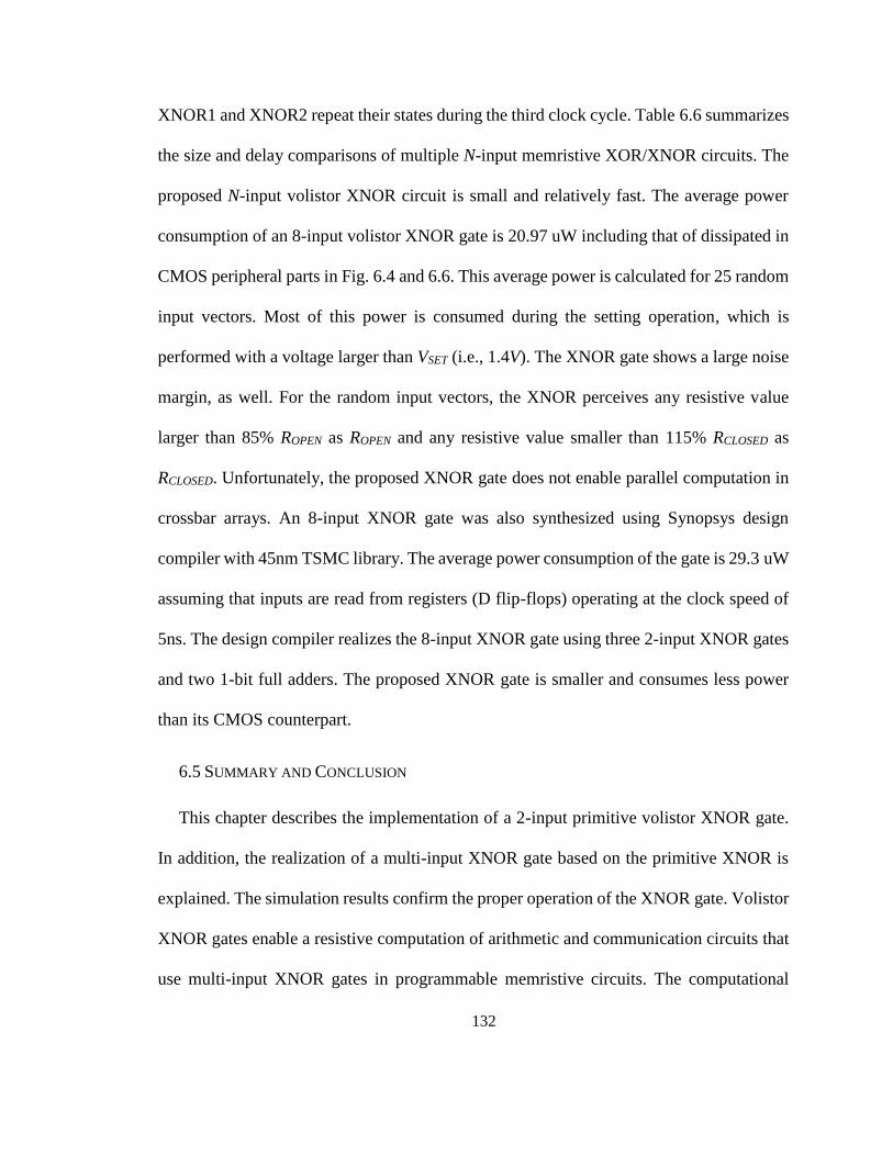
132
XNOR1 and XNOR2 repeat their states during the third clock cycle. Table 6.6 summarizes
the size and delay comparisons of multiple N-input memristive XOR/XNOR circuits. The
proposed N-input volistor XNOR circuit is small and relatively fast. The average power
consumption of an 8-input volistor XNOR gate is 20.97 uW including that of dissipated in
CMOS peripheral parts in Fig. 6.4 and 6.6. This average power is calculated for 25 random
input vectors. Most of this power is consumed during the setting operation, which is
performed with a voltage larger than VSET (i.e., 1.4V). The XNOR gate shows a large noise
margin, as well. For the random input vectors, the XNOR perceives any resistive value
larger than 85% ROPEN as ROPEN and any resistive value smaller than 115% RCLOSED as
RCLOSED. Unfortunately, the proposed XNOR gate does not enable parallel computation in
crossbar arrays. An 8-input XNOR gate was also synthesized using Synopsys design
compiler with 45nm TSMC library. The average power consumption of the gate is 29.3 uW
assuming that inputs are read from registers (D flip-flops) operating at the clock speed of
5ns. The design compiler realizes the 8-input XNOR gate using three 2-input XNOR gates
and two 1-bit full adders. The proposed XNOR gate is smaller and consumes less power
than its CMOS counterpart.
6.5 SUMMARY AND CONCLUSION
This chapter describes the implementation of a 2-input primitive volistor XNOR gate.
In addition, the realization of a multi-input XNOR gate based on the primitive XNOR is
explained. The simulation results confirm the proper operation of the XNOR gate. Volistor
XNOR gates enable a resistive computation of arithmetic and communication circuits that
use multi-input XNOR gates in programmable memristive circuits. The computational

133
delay of the XNOR circuit is small compared to other programmable memristive XNOR
gates. In addition, the power and area comparisons show the benefits of the volistor XNOR
gate over the CMOS XNOR gate.

134
Chapter 7
Volistor Logic Gates in Crossbar Arrays of Rectifying Memristors
This chapter introduces new implementations for volistors and programmable diode
gates in crossbar arrays of rectifying memristors. Volistors use voltage as input and
resistance as output and rely on the diode-like behavior of rectifying memristors. The
design constraints of volistors are explained. These constraints determine the size of the
crossbar array and the voltage levels for logic functions implementations. This chapter
shows that volistors can be cascaded in crossbar arrays with other memristive gates such
as programmable diode gates. An implementation example of AND-NOR PLA based on
hybrid programmable diode gates and volistors in a crossbar array is explained. The hybrid
PLA circuit reduces both area and computational delay. The hybrid PLA circuit is
compared to other memristive PLA (mPLA) circuits realized with stateful gates,
complementary resistive switches (CRS) based gates, and Boolean gates. The outcomes
show the benefit of the hybrid PLA circuit in terms of both size and delay.
7.1 INTRODUCTION
Memristors are the fourth passive basic elements in addition to resistors, capacitors, and
conductors [3]. Memristors are two-terminal, non-volatile, and nanoscale devices. These
devices with fast switching ability can be integrated with transistors [43] and can be scaled
down to less than 10 nm [83] where the size of the transistor is hitting the physical limit.
Memristors can be used for memory applications [15], [40], [84] and for digital and analog
computations [18], [85]-[86]. Memristive digital gates can be divided into three categories.
In the first category, the resistance states of memristors represent logic values [20], [25],

135
[28], [87]-[89]. This type of gates are known as stateful. In the second category, a
combination of resistance (states of memristors) and voltage signals represents logic values
[29], [62], [90]. And in the third category, voltage signals represent the input and output
values [24], [27], [32], [33], [37], [72], [91]-[93]. The stateful gates are sequential gates,
but their realization in parallel can reduce the delay [47], [77]-[78]. The stateful gates are
usually realized in crossbar arrays, however, their realization in structures other than
traditional crossbar arrays is possible [94]. In the second category, gates are designed to
exploit the voltage-based input (or output) of CMOS gates and resistor-based input (or
output) of stateful gates. The realization of logic gates using the Akers array [90], two-
input XOR gate [62], and volistor gates [29] are just a few examples of the second type of
gates. Some of these gates can be realized in crossbar arrays such as the volistors explained
in this chapter. The third category of memristive gates is beneficial to extend Moore’s law
when CMOS scaling becomes problematic. A few examples of this type of gates are
memristive fuzzy logic gates [24], memristive-ratioed logic gates [27], memristive
programmable diode gates [37], Boolean logic gates [91], memristive threshold gates [33]
and [72], memristive stochastic gates [92]-[93], memristive reservoir gates [32], etc. These
gates are not necessarily realized in standard crossbar arrays.
This chapter explains how rectifying memristors [15], [45]-[46] improve logic
operations. We propose a novel approach for implementing volistor gates in crossbar
arrays. Volistors depend on rectifying memristors (i.e., memristors with intrinsic diode-
like behavior) and use voltage as input and resistance as output. In addition, we derive the
design constraints for volistor gates. These constraints determine the size of the crossbar
arrays and the voltage values for realizing the gates. There are two different

136
implementation approaches for volistor gates. In the first approach, volistors use voltage
as input and resistance as output. However, in the second approach, volistors use a mix of
voltage and resistance as input and resistance as output. The second approach realizes, what
we call, input-volistor gates (i.e., input-voltage-resistor and output-resistor gates).
Volistors show some beneficial features. First, volistors enable in-memory computing.
Second, the fan-in and fan-out of volistor gates are large. For example, implementing a 64-
input (output) volistor gate without an auxiliary circuit [44] is not a challenge (see Section
7.6). Third, the voltage-based inputs of volistor gates (in contrast to the resistance-based
inputs of stateful gates) results in a smaller and faster memristive circuits (see Section
7.7.3). And fourth, volistors and other memristive gates can be cascaded in crossbar array
to decrease the delay. For example, AND-NOR functions can be realized in two clock
cycles by cascading volistors and programmable diode gates [37] in crossbar arrays (see
Section 7.7).
The rest of this chapter is organized as follows. In Section 7.2, the structure of memristive
circuit for realizing volistor gates is introduced. Section 7.3 provides a quick review of
volistor gates realized in one-dimensional array, whereas Section 7.4 describes the
implementation of volistor gates and Section 7.5 explain the implementation of input-
volistor gates in crossbar arrays. Section 7.6 shows the design constraints of volistors.
Section 7.7 shows an implementation example of an AND-NOR function based on
programmable diode gates and volistors. The size and delay of the circuit are also compared
to equivalent memristive circuits implemented with other memristive gates. Section 7.8
concludes the paper.

137
7.2 CIRCUIT STRUCTURE FOR VOLISTOR LOGIC GATES
This section shows a general new circuit structure for logic operations based on volistors,
programmable diode gates, stateful gates, etc. Fig. 7.1 illustrates this new circuit structure.
The circuit consists mainly of a computational array and memory array forming our
proposed approach to in-memory computing enabled by memristor technology. The
computational array is a network of sub-crossbar arrays that implements arbitrary logic
operations and store logic values. These sub-crossbar arrays communicate through
columns and rows of pass transistors. The computational array and the pass transistors are
driven by peripheral circuits. These peripheral circuits are controlled by nearby big
memristor memory array, which stores the instructions and control signals. The x columns
of the memory array are controlled by an x-bit shifter. The output of the shifter
............
...
...
...
............
...
...
...
...
...
...
...
...
...
...
...
...
...
Control Circuits
Co
ntro
l Circu
its
Input Array
(Inputs and their Complements)
Computational Array
Memory Array
(Instructions and Control Signals)
x
CMOS Memory Drivers
k
Memory Drivers
Fig. 7.1. General circuit structure for logic computations based on volistor and stateful gates.

138
1 2( , , , )xQ Q Q at the first, second, and xth clock cycle is (1,0, ,0), (0,1,0, ,0), and
(0, ,0,1), respectively, where logic ‘1’ and ‘0’ denote high and low-voltage levels. There
is a relatively small crossbar array that stores a number of k-bit vectors of inputs and their
complements. This input array is connected to the upper peripheral circuits, as illustrated
in Fig. 7.1. In this chapter, we assume that the inputs applied to the computational array
satisfy 0inl inh CLOSE
V v v V where inlv and inhv are low and high input voltages,
respectively, and are chosen 0V and 0.6V .
Let the size of each sub-crossbar array be A B . The size of resistive memory is
(( ) ) nA B C S C where is the number of control signals applied to each
CMOS driver that is connected to a row of the crossbar arrays, is the number of control
signals applied to each CMOS driver that is connected to a column of the crossbar arrays,
C is the number of sub-crossbar arrays, S is the number of pass transistors, and Cn is the
computational delay measured as the number of clock cycles. Here, we assume that 5
and 6 . As a result, the memory bus width is (5 6 )W A B C S . In addition, each
CMOS driver that controls a horizontal or vertical wire consists of five or six transistors,
respectively. Table 7.1 shows the voltage levels used in the circuit in Fig. 7.1 where
inhv v and inhv v . The circuit in Fig. 7.1 performs NOR, AND, INH (inhibition), and
Table 7.1
Voltage levels required during the operations
Operation Required Voltage Levels
Initialization 0V, VSET
Execution VCLEAR, v0 ,־V, v+, |VCLEAR|
Read v0 ,־V, v+

139
COPY gates among other types of logic gates. Each of these gates (except for COPY) has
multiple implementations depending on inputs locations (Table 7.2). For example, NOR
operation can be applied to either the inputs located in the input array (case 1) or the inputs
located in both the input array and computational array (case 2). Let input voltages inlv and
inhv encode logic ‘0’ and logic ‘1’, and input resistances OPENR and
CLOSEDR encode logic
‘0’ and logic ‘1’, respectively. Section 7.3 provides a quick review of volistor gates and
input-volistor gates realized in one-dimensional arrays and shows the limitations of volistor
logic gates.
7.3 REVIEW OF VOLISTOR GATES IN ONE-DIMENSIONAL ARRAYS
Volistors capitalize on diode-like behavior of rectifying memristors and use voltage as
input and resistance as output [29]. The input voltages of volistor gates eliminate the need
for reference resistors, the most power-hungry circuit elements in stateful IMPLY gate
[20], AND gate [88], CNIMP (Converse Non-Implication) gate [25], etc. Section 7.3.1
reviews the implementation of volistor NOR gate and its limitations, and Section 7.3.2
reviews the implementation of input-volistor NOR gate (which uses a mix of voltage and
resistance as input and resistance as output).
Table 7.2
Volistor operations and their input locations
Case
Inputs Locations Gates
Input
Array
Computational
Array NOR AND INH COPY
1
2
3

140
7.3.1 Volistor NOR gate
Volistor NOR gate was introduced in [29]. This implementation approach has the inputs
stored in the input array. Fig. 7.2 shows the schematic of an n-input volistor NOR gate
realized in a 1 ( 1)n memristive array with the voltages specified in (7.1).
0
0
inl inh CLOSE
OPEN T
T inh CLEAR
V v v V
V V V
V v V
(7.1 )
(7.1 )
(7.1 )
a
b
c
The role of each memristive switch is determined by its driving voltage such as v+, v־, etc.
Memristive switches S are set to closed state and connected to input voltages vin1-vinn. The
target memristive switch (which stores the output) is connected to voltage VT. Volistor
NOR is implemented in two clock cycles. In the first clock cycle, switch T is set closed.
And in the second clock cycle, NOR gate is implemented. Though memristive switches are
set closed, some of them act as open switches. For example, memristive switch T is always
reverse biased and acts as an open switch. During the operation, all switches S remain
closed. However, the state of switch T may be changed to open (programmed to HRS).The
diode-like behavior of memristors allows the implementation of volistor gates that have
multiple fan-out without auxiliary circuits [44]. When at least one of the inputs is high, the
voltage on wire wm is approximately vinh. Therefore, the voltage across switch T is close to
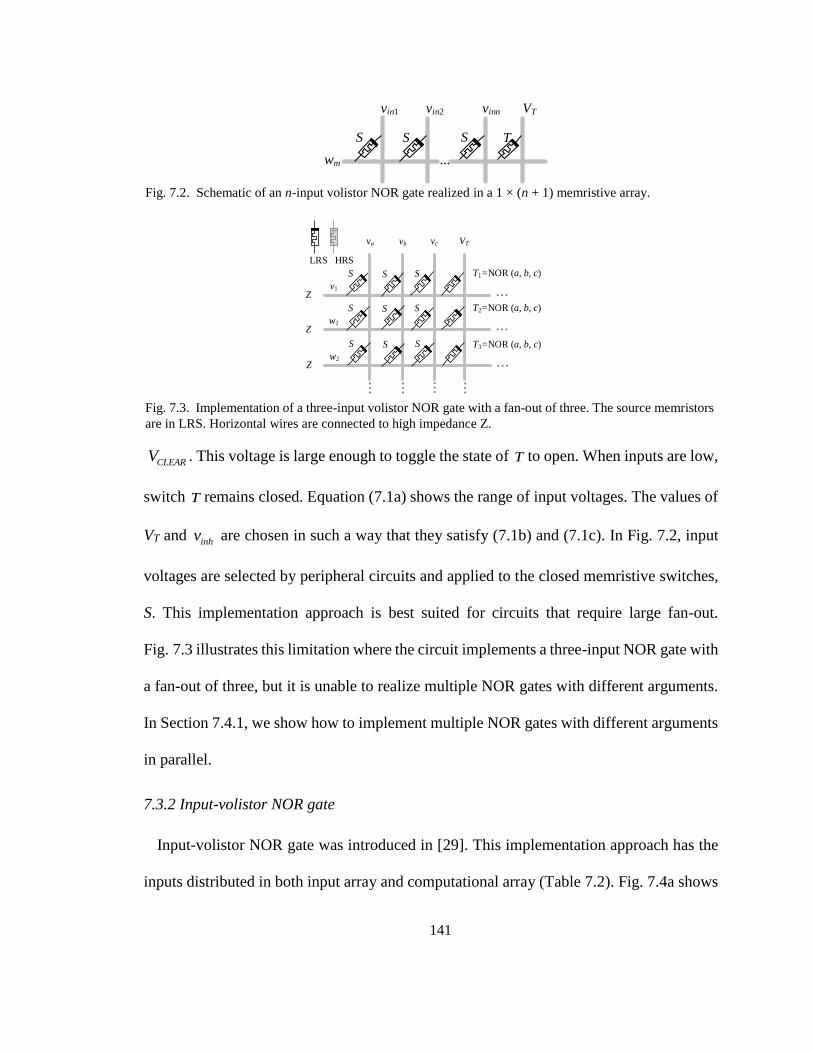
141
CLEARV . This voltage is large enough to toggle the state of T to open. When inputs are low,
switch T remains closed. Equation (7.1a) shows the range of input voltages. The values of
VT and inhv are chosen in such a way that they satisfy (7.1b) and (7.1c). In Fig. 7.2, input
voltages are selected by peripheral circuits and applied to the closed memristive switches,
S. This implementation approach is best suited for circuits that require large fan-out.
Fig. 7.3 illustrates this limitation where the circuit implements a three-input NOR gate with
a fan-out of three, but it is unable to realize multiple NOR gates with different arguments.
In Section 7.4.1, we show how to implement multiple NOR gates with different arguments
in parallel.
7.3.2 Input-volistor NOR gate
Input-volistor NOR gate was introduced in [29]. This implementation approach has the
inputs distributed in both input array and computational array (Table 7.2). Fig. 7.4a shows
LRS HRS
S S S
S S S
S S S
...
...
...
...
...
...
...
va vb vc VT
v1
w2
w2
Z
Z
Z
T1=NOR (a, b, c)
T2=NOR (a, b, c)
T3=NOR (a, b, c)
Fig. 7.3. Implementation of a three-input volistor NOR gate with a fan-out of three. The source memristors
are in LRS. Horizontal wires are connected to high impedance Z.
VTvinnvin2vin1
...
S SS T
wm
Fig. 7.2. Schematic of an n-input volistor NOR gate realized in a 1 × (n + 1) memristive array.

142
the schematic of the two-input-volistor NOR gate with input voltage va, input resistance rb,
and output resistance rT, as such rb and rT denote the logical states of S2 and T, respectively.
Input va is applied to memristor S1 initialized to LRS, voltage v+ is applied to memristor S2,
and voltage VT is applied to memristor T. The circuit operates with the voltages specified
in (7.1). An n-input-volistor NOR gate is realized in a 1 × (n + 1) memristive array. The
correct operation of volistor NOR may require grounding wm through reference resistor Rg
when n ≥ 8 (Fig. 7.4b). The need for Rg appears when all of the inputs are logic ‘0’, and
most of the inputs are resistances. Fig. 7.4b illustrates an n-input-volistor NOR circuit with
n-1 input resistance at logic ‘0’ (HRS) and one input voltage at logic ‘0’ ( inlv ). For this
combination of inputs, the circuit must satisfy (7.1) where
(( 1) 1) / ( )m T gw n v V n N
and OPEN ggN R R . For v+ = 0.6V, VT = -0.6V, and
Rg=√ (ROPRN × RCLOSED), Equation (7.2) is simplified to n < 74. In fact, the use of reference
resistor Rg allows to increase the size of the input-volistor NOR gate from n < 8 to n < 74.
v+va VT
S1
rb
wm
TS2
rT
(a)
v+vinl VT
S1
wm
TS2
v+
S3
v+
Sn
...
LRS HRS
Rg
(b)
Fig. 7.4. (a) Schematic of two-input-volistor NOR gate. Inputs are va and rb, and the output is rT. (b)
Schematic of an n-input-volistor NOR gate where all of the inputs are logic ‘0’.

143
When n < 8, the circuit can operate without Rg where )(( 1) ( 1)m T
w n v V n .
m T OPEN
w V V (7.2)
7.4 VOLISTOR GATES IN TWO-DIMENSIONAL ARRAYS
This section explains the implementation of improved volistor NOR, volistor AND, and
volistor COPY gates in crossbar arrays and show how to deselect a volistor gate in a
crossbar array.
7.4.1 Improved volistor NOR gate
In a single crossbar array, identical gates with identical inputs are a limited form of
parallelism that can be realized using volistor logic (Fig. 7.3). This limitation could be
resolved by permanently disabling specific memristors in the crossbar array that leaves
those memristors in permanent HRS [18], [75]. This approach would result in an
application-specific integrated circuit, different than our general concept of a
programmable mPLA. As an alternative, in our approach, the rectifying memristors are
programmed to HRS taking the role of memristors in permanent HRS. Recall that the
rectifying memristors have relatively large ROPEN and ROPEN/RCLOSED ratio. Consequently,
input voltages can be disconnected by programming the source memristors to HRS. This
technique allows to implement multiple volistor NOR gates in parallel in a crossbar array.

144
For example, the crossbar array shown in Fig. 7.5 implements Tm = NOR (a, b, c) on wire
and Tm+1 = NOR (¬a, ¬b, ¬c) = AND (a, b, c) on wm+1. The source memristors on wm+2 are
programmed to HRS to disconnect the inputs. The gates can be executed for any input
vector [va, vb, vc] in two clock cycles as the inputs are voltage signals and the source
memristors retain their resistance states. In contrast, the implementations of stateful logic
gates require programming the source memristors for any input vector of literals, because
the resistance states of source memristors represent the input values. In stateful gates,
programming the source memristors takes more clock cycles (e.g. 2n where n is the
number of inputs [25]) than in volistors where the programming takes only a single cycle.
In stateful logic, we would apply a voltage of v+/2 (v2/־) to those rows which are not used
in the current operation of the crossbar array [95]. This would prevent the target memristors
in these “deselected” rows from changing states. In contrast, in our circuit shown in
Fig. 7.1, to deselect a row of volistor NOR or any other row in a crossbar array, a
conventional v+/2 scheme cannot be used. Section 7.4.2 shows how to deselect a volistor
gate in a crossbar array.
LRS HRS
Tm = NOR (a, b, c)S SS S S S
...
Tm+1 = NOR (¬ a, ¬ b, ¬ c)S SS S S
...
Tm+2 = 1S SS S S S
...
...
...
...
...
...
...
...
S
va v¬ a vb v¬ b vc v¬ c VT
wm
wm+1
wm+2
Fig. 7.5. Implementation example of multiple volistor NOR gates in a crossbar array. The circuit
implements Tm = NOR (a, b, c) on wm and Tm+1 = NOR (¬a, ¬b, ¬c) on wm+1. Source memristors on wm + 2
are in HRS to disconnect the input voltages.
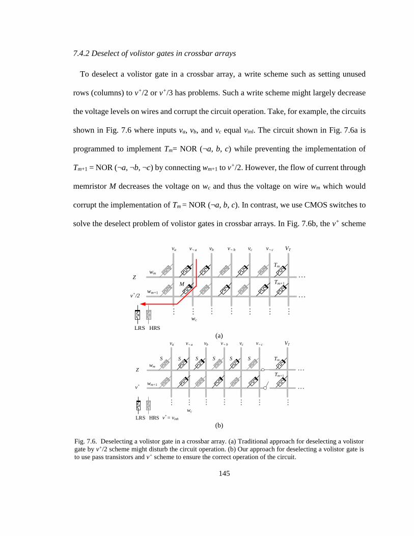
145
7.4.2 Deselect of volistor gates in crossbar arrays
To deselect a volistor gate in a crossbar array, a write scheme such as setting unused
rows (columns) to v+/2 or v+/3 has problems. Such a write scheme might largely decrease
the voltage levels on wires and corrupt the circuit operation. Take, for example, the circuits
shown in Fig. 7.6 where inputs va, vb, and vc equal vinl. The circuit shown in Fig. 7.6a is
programmed to implement Tm= NOR (¬a, b, c) while preventing the implementation of
Tm+1 = NOR (¬a, ¬b, ¬c) by connecting wm+1 to v+/2. However, the flow of current through
memristor M decreases the voltage on wc and thus the voltage on wire wm which would
corrupt the implementation of Tm = NOR (¬a, b, c). In contrast, we use CMOS switches to
solve the deselect problem of volistor gates in crossbar arrays. In Fig. 7.6b, the v+ scheme
LRS HRS
Tm
...
...
...
...
...
...
...
...
...
va v¬ a vb v¬ b vc v¬ c VT
wm
wm+1
Z
v+/2
Tm+1
wc
M
(a)
LRS HRS
Tm S SS S S S
...
...
...
...
...
...
...
...
...
va v¬ a vb v¬ b vc v¬ c VT
wm
wm+1
Z
v+
wc
Tm+1
v+= vinh (b)
Fig. 7.6. Deselecting a volistor gate in a crossbar array. (a) Traditional approach for deselecting a volistor
gate by v+/2 scheme might disturb the circuit operation. (b) Our approach for deselecting a volistor gate is
to use pass transistors and v+ scheme to ensure the correct operation of the circuit.
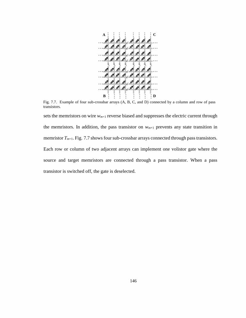
146
sets the memristors on wire wm+1 reverse biased and suppresses the electric current through
the memristors. In addition, the pass transistor on wm+1 prevents any state transition in
memristor Tm+1. Fig. 7.7 shows four sub-crossbar arrays connected through pass transistors.
Each row or column of two adjacent arrays can implement one volistor gate where the
source and target memristors are connected through a pass transistor. When a pass
transistor is switched off, the gate is deselected.
...
...
...
............
............
............
...
...
...
...
...
...
...
...
............
...
...
...
...
...
A
B
C
D
Fig. 7.7. Example of four sub-crossbar arrays (A, B, C, and D) connected by a column and row of pass
transistors.
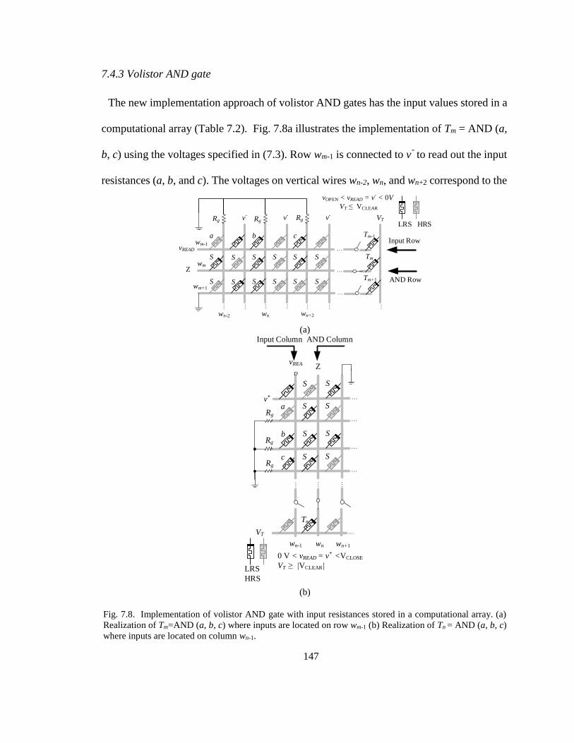
147
7.4.3 Volistor AND gate
The new implementation approach of volistor AND gates has the input values stored in a
computational array (Table 7.2). Fig. 7.8a illustrates the implementation of Tm = AND (a,
b, c) using the voltages specified in (7.3). Row wm-1 is connected to v־ to read out the input
resistances (a, b, and c). The voltages on vertical wires wn-2, wn, and wn+2 correspond to the
LRS HRS
wm-1
a
v-v-
b c
v-
...vREAD
...
... ...
...
...
...
wm
S SS S S S
...Z
Tm-1
...
VT
Tm
vOPEN < vREAD = v- < 0V
VT VCLEAR
RgRgRg
wm+1
...
S SS S S STm+1
wn-2 wn wn+2
Input Row
AND Row
(a)
LRS
HRS
b
...
a
...
...
...
vREA
D
...
Z
...VT
c
...
wnwn-1
Tn
S
S
S
S
0 V < vREAD = v+ <VCLOSE
VT |VCLEAR|
v+
Rg
Rg
Rg
...
wn+1
S
S
S
S
Input Column AND Column
(b)
Fig. 7.8. Implementation of volistor AND gate with input resistances stored in a computational array. (a)
Realization of Tm=AND (a, b, c) where inputs are located on row wm-1 (b) Realization of Tn = AND (a, b, c)
where inputs are located on column wn-1.

148
inputs. The output of the AND gate is the resistance state of memristor Tm connected to
horizontal wire wm. Memristor Tm is driven by voltage VT. The other memristors on m
w are
not part of the AND gate and are connected to v־ in order to minimize the effect of the
sneak current paths. Horizontal wires except for wm-1 and wm are connected to the GND.
The pass transistors are switched off, except for the one that is connected to Tm. If the inputs
were located in a column of the crossbar array, the AND gate would be implemented using
the voltages specified in (7.4). Fig. 7.8b illustrates the implementation of Tn = AND (a, b,
c) where inputs a, b, and c are located in column wn-1 and the output is stored in memristor
Tn. A two-input AND gate was simulated in a 9 × 9 crossbar array using 50 nm TSMC
process and the SPICE model of the rectifying memristor [47]. The simulation results show
the correct operation of the AND gate for all input combinations. Note that volistor AND
gate can also be implemented using input complements stored in the input array in the same
manner of implementing volistor NOR gate shown in Section 7.4.1.
0
OPEN
T CLEAR
V v V
V V
(3)
0
CLOSE
T CLEAR
V v V
V V
(4)
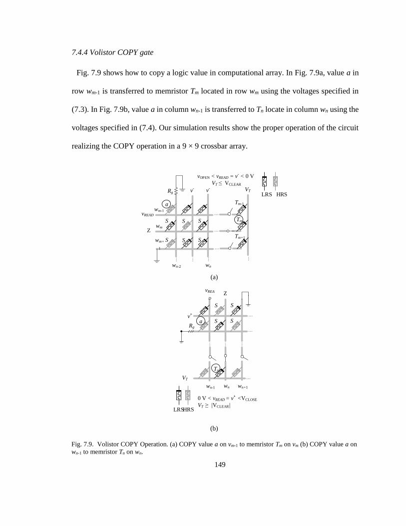
149
7.4.4 Volistor COPY gate
Fig. 7.9 shows how to copy a logic value in computational array. In Fig. 7.9a, value a in
row wm-1 is transferred to memristor Tm located in row wm using the voltages specified in
(7.3). In Fig. 7.9b, value a in column wn-1 is transferred to Tn locate in column wn using the
voltages specified in (7.4). Our simulation results show the proper operation of the circuit
realizing the COPY operation in a 9 × 9 crossbar array.
LRS HRS
wm-1
a
v-
...vREAD
...
...
...
wm
S S S
...Z
Tm-1
...
VT
Tm
vOPEN < vREAD = v- < 0 V
VT VCLEAR
Rg
wm+
1 ...
S S STm+1
wn-2 wn
v-
(a)
LRS HRS
......
vREA
D
...
Z
...VT
a
...
wnwn-1
Tn
S
S
0 V < vREAD = v+ <VCLOSE
VT |VCLEAR|
v+
Rg
...
wn+1
S
S
(b)
Fig. 7.9. Volistor COPY Operation. (a) COPY value a on vm-1 to memristor Tm on vm (b) COPY value a on
wn-1 to memristor Tn on wn.

150
In Section 7.5, the input-volistor INH gate and input-volistor AND gate are proposed.
These logic gates use a mix of voltage and resistance as input and resistance as output.
7.5 INPUT-VOLISTOR GATES IN TWO-DIMENSIONAL ARRAYS
The implementation of input-volistor INH requires having the inputs distributed in both
the input array and computational array. However, the implementation of input-volistor
AND gate requires having the inputs distributed in two different columns (rows) of
adjacent sub-crossbar arrays (Table 7.2).
7.5.1 Input-volistor INH gate
By definition, a INH b= (¬a) b, which also equals ¬ ((¬a) IMPLY (¬b)). The INH gate
is implemented with two memristors, as shown in Fig. 7.10, where va is the input voltage
and rb is the input resistance. Input va is applied to source memristor S initialized to LRS,
and input rb is the initial state of memristor T. The output is the new resistance state of
memristor T. The INH gate is implemented using the voltages specified in (7.1). Our
simulation results confirm the correct operation of the INH gate for all input combinations.
INH along with constant ‘1’ form a functionally complete set of logic gates. The input-
volistor IHN is implemented similar to input-volistor NOR. The difference is that in input-
VTva
S T
wr
rb
Fig. 7.10. Schematic of input-volistor INH gate. Inputs are va and rb, and the output is (¬a) b, which updates
resistance state rb of memristor T.

151
volistor NOR, the output is separated than inputs whereas in input-volistor INH, the output
is represented on the same memristor as one of the inputs.
7.5.2 Input-volistor AND gate
The input-volistor AND gate is implemented similar to the volistor AND gate (Fig. 7.8
The difference is that in input-volistor AND the output is represented on the same
memristor as one of the inputs whereas in volistor AND the output is separated than inputs.
In Section 7.6, the design constraints for implementing volistor gates in crossbar arrays
are discussed.
7.6 DESIGN CONSTRAINTS OF VOLISTOR GATES IN CROSSBAR ARRAYS
Volistors operate in crossbar arrays under some constraints. These constraints determine
the size of computational array and the range of voltage levels for implementing the gates.
The constraints are obtained under the assumption of having the primary inputs and their
complements stored in the input array. In addition, it is assumed that v+ = vinh, v־ = -vinh,
and Rg = √ (ROPEN×RCLOSED) where Rg is the reference resistor. Moreover, the pass
transistors connecting the sub-crossbar arrays are chosen such that rds << RCLOSED ˂˂ ROPEN
where rds is the drain-source resistance of a pass transistor. The constraints are explained
for each volistor gate as follows.
7.6.1 Design constraints of improved volistor NOR gate
Constraint 1 to Constraint 3 must be satisfied for the improved volistor NOR gates,
realized in two m × n sub-crossbar arrays.
Constraint 1. If all of the NOR’s inputs are logic ‘0’, the closed state of target memristive

152
switch must remain closed. In other words, Equation (7.2) should be satisfied where
(( 0.5) ) / 2m Tv n v V n . Fig. 7.11 shows the VT-n relation for the applied inputs. This
VT-n relation is denoted by ‘lower_all_0’ and shows the lower bound of VT.
Constraint 2. If one of the NOR’s inputs is logic ‘1’, the closed state of target memristive
switch must toggle to open. In other words, Equation (7.5) should be satisfied where
(( 1.5) ) / ( 2 1)m Tv N n v V N n and /OPEN CLOSEDN R R . Substituting vm in
(7.5) results in (7.6), which determines the range of VT. Fig. 7.11 shows the VT-n relations
for the applied inputs. These relations are denoted by ‘lower_1’ and ‘upper_1’ and show
the boundaries of VT.
2CLEAR OPEN CLEARm TV V v V V (7.5)
( 1.5)
2 2T CLEAR
N n vV V
N n
(7.6a)
( 1.5) ( 2 1) 2
2 2
CLEAR OPEN
T
N n v N n V VV
N n
(7.6b)
Constraint 3. If all of the NOR’s inputs are logic ‘1’, the closed state of target memristive
switch must toggle to open. In other words, Equation (7.5) should be satisfied where
( ( 0.5) ) / ( ( 0.5) ( 0.5))Tvm N n v V N n n . Fig. 7.11 shows the VT-n relations
for the applied inputs. These relations are denoted by ‘lower_all_1’ and ‘upper_all_1’ and
show the lower and upper bound of VT.

153
The shaded area in Fig. 7.11 shows the range of VT for realizing i-input volistor NOR
gates for any combination of inputs where i ≤ n - 1. Note that the resistive effect of the
wires is negligible as the resistance of the wires is very small compared to RCLOSED =
500 KΩ. For example, the resistive value of a relatively large width wire of diameter
120 nm used in a 32 × 32 crossbar array is at most 30 KΩ when implemented with relatively
high resistance p-doped Si [61]. In other words, the resistive value of each wire is about
1 KΩ, which is very small compared to RCLOSED.
Fig. 7.12b shows the simulation results of three 50-input volistor NOR gates realized in
a 3 × 101 crossbar array where inputs are (0, 0, …, 0), (1, 0… 0), and (1, 1, …, 1). The
state transition delay in target memristors depends on the number of vinh applied to each
NOR gate. The longest delay occurs when only one of the inputs is high. In this case, the
delay is 4.67 ns, which is 11.75% longer than a 4 ns transition delay in LRS memristor
connected to VCLEAR (Fig. 7.12a).
Fig. 7.11. VT-n relations of multiple volistor NOR gates realized in two m × n crossbar arrays. The
shaded area shows the range of VT for implementing i -input volistor NOR gates where i ≤ n - 1.
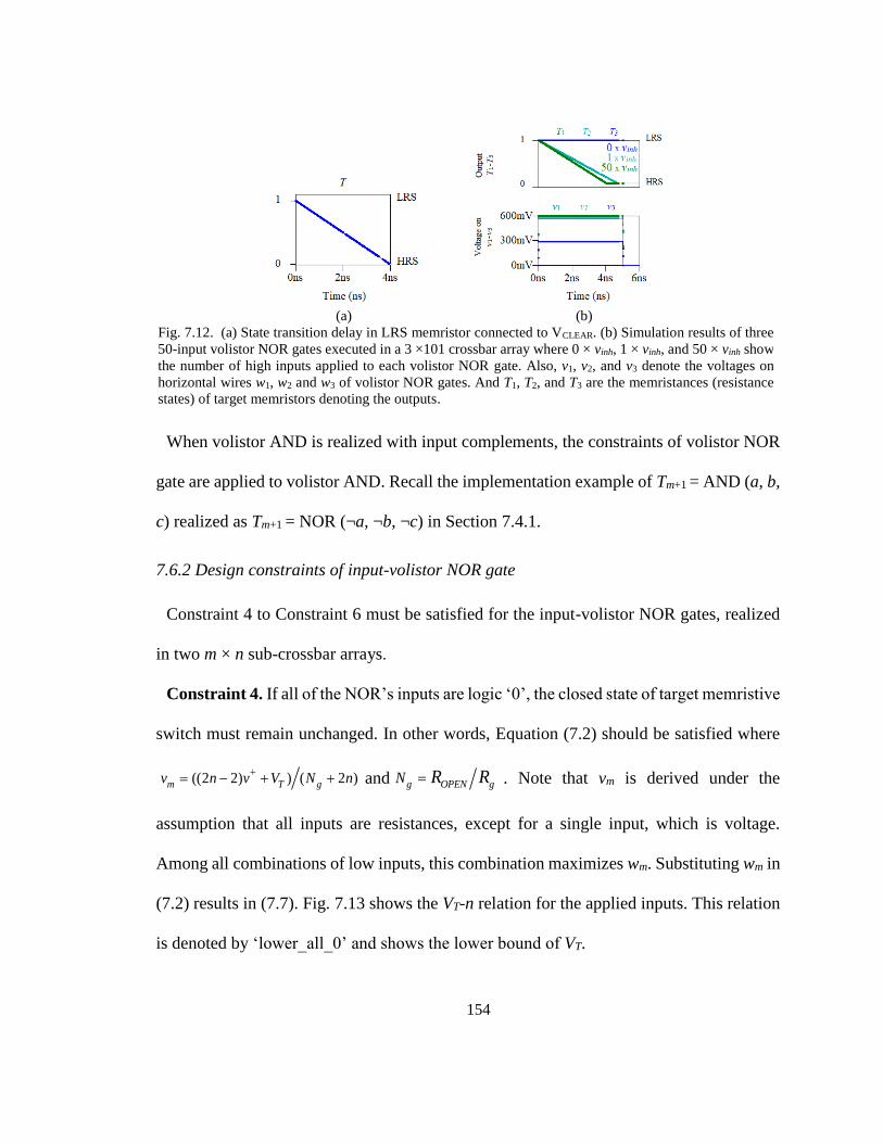
154
When volistor AND is realized with input complements, the constraints of volistor NOR
gate are applied to volistor AND. Recall the implementation example of Tm+1 = AND (a, b,
c) realized as Tm+1 = NOR (¬a, ¬b, ¬c) in Section 7.4.1.
7.6.2 Design constraints of input-volistor NOR gate
Constraint 4 to Constraint 6 must be satisfied for the input-volistor NOR gates, realized
in two m × n sub-crossbar arrays.
Constraint 4. If all of the NOR’s inputs are logic ‘0’, the closed state of target memristive
switch must remain unchanged. In other words, Equation (7.2) should be satisfied where
((2 2) ) ( 2 )m T gv n v V N n
and g OPEN gN R R . Note that vm is derived under the
assumption that all inputs are resistances, except for a single input, which is voltage.
Among all combinations of low inputs, this combination maximizes wm. Substituting wm in
(7.2) results in (7.7). Fig. 7.13 shows the VT-n relation for the applied inputs. This relation
is denoted by ‘lower_all_0’ and shows the lower bound of VT.
(a) (b)
Fig. 7.12. (a) State transition delay in LRS memristor connected to VCLEAR. (b) Simulation results of three
50-input volistor NOR gates executed in a 3 ×101 crossbar array where 0 × vinh, 1 × vinh, and 50 × vinh show
the number of high inputs applied to each volistor NOR gate. Also, v1, v2, and v3 denote the voltages on
horizontal wires w1, w2 and w3 of volistor NOR gates. And T1, T2, and T3 are the memristances (resistance
states) of target memristors denoting the outputs.

155
(( 1) (2 ) (2 ) ) ( 2 1)OPENT g gV n v n N V N n
(7.7)
Constraint 5. If one of the NOR’s inputs is logic ‘1’, the closed state of target memristive
switch must toggle to open. In other words, Equation (7.5) should be satisfied where
( 1)
2 1 ( ) ( ) 1(2 1) 1T
mg g
n v V vw
N N n n N N
. Note that wm is derived under the assumption
that the high input is resistance while all other inputs are voltages. Among all combinations
of inputs (for which only one input is logic ‘1’), this combination of inputs minimizes wm.
Fig. 7.13 shows the VT-n relations for the applied inputs. These relations are denoted by
‘lower_1’ and ‘upper_1’ and show the lower and upper bounds of VT.
Constraint 6. If all of the NOR’s inputs are logic ‘1’, the closed state of target memristive
switch must toggle to open. In other words, Equation (7.5) should be satisfied where
(2 2) 2(( ) ( ))( ) 11 2 1 (2 2)mgg
VTv
N N nv
N N n
. Note that wm is derived under the
assumption that all inputs are resistances, except for a single input, which is voltage.
Among all combinations of high voltage-resistance inputs, this combination maximizes vm.
Fig. 7.13 shows the VT-n relations for the applied inputs. These relations are denoted by
‘lower_all_1’ and ‘upper_all_1’ and show the boundaries of VT. The shaded area in
Fig. 7.13 shows the range of VT for realizing an i-input-volistor NOR gate for any
combination of inputs where i ≤ 2n - 2. The input-volistor NOR gate is realized in a smaller
computational array than the array used for volistor NOR gate. The small number of inputs

156
is an outcome of Constraint 4. Therefore, realizing both types of volistor NOR gate requires
small sub-crossbar arrays.
7.6.3 Design constraints of input-volistor AND gate
Constraint 7 to Constraint 9 must be satisfied for the volistor AND (and input-volistor)
gates, realized in two m × n sub-crossbar arrays.
Constraint 7. If all of the AND’s inputs are logic ‘1’, the close state of target memristive
switch must remain closed. Therefore, Constraint (7.8) should be satisfied where vn is the
voltage on wire wn (see Fig. 7.8) and equals ( (2 1) ) ( (2 1) 1)TN m v V N m . Fig.
7.14 shows the VT-m relation for the applied inputs. This relation is denoted by
‘upper_all_1’ and it shows the upper bound of VT.
n T OPENv V v (7.8)
Constraint 8. If one of the AND’s inputs is logic ‘0’ while all other inputs are logic ‘1’
the closed state of target memristive switch must toggle to open. In other words, Equation
(7.9) should be satisfied where ((2 2) ) ( 2 1)n Tv m v V N m . Fig. 7.14 illustrates
Fig. 7.13. VT–n relations of multiple input-volistor NOR gates realized in two m × n crossbar arrays. The
shaded area shows the range of VT for implementing i-input-volistor NOR gates where i ≤ 2n - 2.

157
the VT-m relations for the applied inputs. These relations are denoted by ‘upper_1L’ and
‘lower_1L’ and show the upper and lower bounds of VT, respectively.
2CLEAR OPEN n T CLEARV V v V V (7.9)
Constraint 9. If all of the AND’s inputs are logic ‘0’, Equation (7.9) should be satisfied
where ( (2 1) 1)n Tv V N m . Fig. 7.14 shows the VT-m relations for the applied inputs.
These relations are denoted by ‘upper_all_0’ and ‘lower_all_0’ and show the boundaries
of VT. Fig. 7.14 shows the range of VT for realizing an i-input volistor AND gate for any
combination of inputs where 2 1i m .
In summary, all volistor gates can be realized in small sub-crossbar arrays. The size of a
sub-crossbar array depends on characteristics of the rectifying memristors summarized in
Table 6.2.
7.7 IMPLEMENTATION EXAMPLE AND COMPARISONS
Volistors can be cascaded with programmable diode gates in the computational array.
We propose a programmable memristive PLA-like circuit (mPLA) for realizing two-level
multi-output functions well-suited for OR-AND based design. The computational delay of
Fig. 7.14. VT-m relations of multiple volistor AND gates realized in two m × n crossbar arrays. The shaded
area shows the range of VT for realizing i-input volistor AND gates where i ≤ 2m-1.

158
the mPLA is two clock cycles. In the first clock cycle, the target memristors are initialized
to LRS, and in the second clock cycle, functions are implemented. The mPLA uses voltage
as input and resistance as output and maintains the states of the source memristors during
the operations. Therefore, calculating a function for a new combination of inputs would
still require two clock cycles. The input levels of functions are implemented with
programmable diode OR gates, and the output levels are realized with volistor AND gates.
In Section 7.7.1, a quick review of memristive programmable diode gates is provided. In
addition, we show how to improve the programmable diode gates for parallel computing
in crossbar arrays. In Section 7.7.2, the programmable mPLA circuit for realizing an
arbitrary POS function based on hybrid diode gates and volistors is introduced. And in
Section 7.7.3, the implementations of POS functions with multiple memristive gates
(proposed in the literature) are compared to our implementation approach.
7.7.1 Memristive programmable diode gates
The memristive programmable diode gates capitalize on rectifying memristors and use
voltage as input and output. The diode gates are realized in a one-dimensional memristive
array. The proper operation of the gates requires programming the memristors to LRS. Let
us focus on the programmable diode OR gate. An n-input diode OR gate is implemented
in a 1 × n memristive array (see Fig. 7.2) using the voltages specified in (7.1). Inputs are
vin1-vinn and the output is vm, the voltage on wire wm. And, memristors maintain their states
during the operations. Inputs are selected by peripheral circuits and applied to the
memristive array. The implementation of diode gates can be improved similar to the

159
volistor gates by programming the memristors to HRS or LRS to disconnect or select an
input voltage, respectively.
7.7.2 Realization of a multi-output AND-OR function in the mPLA
Fig. 7.15 shows the schematic of mPLA for realizing an arbitrary multi-output POS
function. The mPLA consists of two sub-crossbar arrays, A and B, connected through pass
transistors. Sums are realized with diode ORs (e.g., OR 1, OR 2, OR 3) and the products
are implemented with volistor ANDs (e.g., AND n-1, AND n). Inputs are vin1-vinn, and
outputs are the new states of the target memristors (e.g., Tn- 1 and Tn). To deselect an output,
the corresponding AND gate is connected to 0V (e.g., AND n-2), and the relevant pass
transistor is switched off. Memristors in crossbar array A maintain their resistance states.
LRS HRS
OR 3
OR 2
OR 1
...
...
v¬in1
...VT
c2c1
0 V vin < VCLOSE
VT |VCLEAR|
...
c3
...
...
...
0 V Zvin1 v¬in2vin2 Z
...
...
...
...
cn-1cn-2
Tn-1
cn
...
...
...
...
...
...
...
c4
AN
D n
AN
D n
-1
Tn
v3
v2
v1
A
B
AN
D n
- 2
Fig. 7.15. Schematic of the mPLA for realizing a multi-output POS function.

160
As a result, calculating the function for another combination of inputs would only require
programming the target memristors to LRS and realizing the function.
A single-output OR-AND function can be realized in a single crossbar array. In this
realization, the size of the crossbar array can be as large as 512 × 512, and the only circuit
constraint to satisfy is to have the inputs and their complements stored in the input memory.
In realizing a single-output OR-AND function, all memristors of volistor AND are
initialized to LRS. To disconnect an input of AND gate, the corresponding horizontal
wired-OR is connected to v+. In Section 7.7.3, we compare the realization of an arbitrary
OR-AND function (or AND-NOR function, when negated inputs are used for realizing the
functions) based on the hybrid approach, and other memristive approaches.
7.7.3 Comparisons of the mPLA implementations
An extensive comparison of different mPLA implementations is beyond the scope of this
dissertation. However, to get some level of comparison, the implementations of proposed
mPLA and other hypothetical mPLAs are evaluated. This evaluation takes into account the
delay and the size of the memory array. The memory array and its CMOS peripheral circuit
dominate the circuit area. Thereby, the size of memory array is used for estimating the size
of the memristive circuit. An n-input single-output AND-NOR function is implemented in
multiple mPLA circuits for comparison.
1) mPLA circuit based on stateful IMPY-CNIMP gates
An n-input AND-NOR function can be implemented using IMPLY and CNIMP (INH)
operations [25] in an ( 1) ( 1)m n crossbar array. The size of memory array, which
stores the instructions and control signals, equals nW C . The delay is estimated to be

161
2 5nC n based on the published data. In addition, the size of memory bus width equals
4 ( 2)W m n as each wire is driven by four control signals [47]. Therefore, the size
of memory array is 4 ( 2) (2 5)m n n .
2) mPLA circuit based on stateful NOR-NOT gates
An n-input AND-NOR function can be realized based on stateful NOR and NOT gates
[28] in an ( 1) ( 1)m n crossbar array. We estimate the delay to be n + 4 clock cycles.
Mapping the function into the crossbar array is performed similar to the approach explained
in [96], i.e., one clock cycle for initializing the memristors to HRS, n + 1 cycles for
programming n + 1 columns of the crossbar array, and two clock cycles for realizing a
function—one cycle for realizing m stateful AND gates (NORs with negated inputs) and
the other cycle for realizing a single NOR gate. We estimate the width of memory bus to
be 3 ( 1) 5 ( 1)W m n , as each horizontal wire is controlled by three signals to be
connected to 0 , HSV V and0V , and each vertical wire is controlled by five signals to be
connected to 0,0 , ,CLEAR VSV V V V and SETV where ,HS VSV V and
0V are used to deselect a row,
to deselect a column, and to realize a gate, respectively. Therefore, the size of the memory
array ( )nW C is (5 3 8) ( 4).n m n
3) mPLA circuit based on CRS-CMOS gates
An n-input AND-NOR function can be implemented using CRS-CMOS gates [97] in two
crossbar arrays of m × n (for realizing the AND gates) and 1 × m (for realizing a NOR
gate). The delay is estimated to be n + 3 that is two cycles for initializing the CRS cells of
each crossbar to HRS/LRS state, n cycles for mapping the function into AND crossbar, and
one cycle for implementing the function. We estimate the width of memory bus to be

162
2 3 ( 1) ( 1)W m n m as each horizontal wire of the AND crossbar is controlled
by two signals to be connected to 0V and VHS (a non-destructive positive voltage) and each
vertical wire is controlled by three signals to be connected to , , ,th n RV V and ,th pV (i.e., a
destructive negative voltage, a non-destructive positive voltage which is equal to HSV , and
a destructive positive voltage, respectively). In addition, each wire of the NOR crossbar is
controlled by one signal to be connected to either 0V or ,th nV (during the initialization step).
Note that VHS is applied to deselect a row in the AND crossbar and VR is applied to
implement AND gates. Therefore, the size of the memory array ( )nW C is
(3 3 4) ( 3).m n n
4) mPLA circuit based on Boolean gates
An n-input NAND-AND function (or equivalently AND-NOR function) can be
implemented with the Boolean AND, NAND, and COPY gates in an ( 1) (2 1)m n
crossbar array [75]. The delay is five clock cycles. That is one cycle for the initialization
of the memristors to HRS, one cycle for copying the inputs and their complements to the
crossbar, one cycle for mapping the function into the crossbar, and two cycles for realizing
the function [75]. We estimate the width of the memory bus to be 4 ( 2 2)W m n as
each horizontal wire is controlled by four signals to be connected to 0 ,V HSV , SETV , and
reference resistor gR , and each vertical wire is controlled by four signals to be connected
to CLEARV , whV , SETV , and gR where Vwh = VHS. Vwh is used for implementing the gates,
whereas VHS is used for deselecting a row. Therefore, the size of memory array ( )nW C
is 20 ( 2 2)m n .

163
5) mPLA circuit based on hybrid gates
In the hybrid circuit, an n-input AND-NOR function can be implemented with hybrid
diode OR and volistor AND gates in an (m + 1) × (2n + 1) crossbar array. The outputs of
diode ORs represent logical NAND of input complements, (i.e., OR (¬a, ¬b) = NAND (a,
b)). Therefore, the mPLA can realize NAND-AND functions (or equivalently AND-NOR
functions). The delay of the mPLA is two clock cycles. In addition, the width of memory
bus is 5 ( 1) 6 (2 1)W m n . Therefore, the size of the memory array is
24 10 22n m .
6) Other circuits
There is another type of mPLA circuits, which use voltage as input and output, e.g., [98].
This type of mPLA was not used for in-memory computing, thereby, it is not compared to
other mPLAs mentioned above.
Fig. 7.16 compares the percentage increase in the memory array for each approach. The
memory percentage increase is defined as ( ) ( )
( ) 100( )
A x A hybF x
A hyb
where ( )A x is the
size of memory array and x1, 2, 3, 4 corresponds to the stateful IMPLY-CNIMP based
mPLA, stateful NOR-NOT based mPLA, CRS-CMOS based mPLA, and Boolean based
mPLA, respectively. In addition, ( )A hyb is the size of memory array in our hybrid based
mPLA. The minimum increase in the memory array occurs in the Boolean based mPLA
for n = 8 and it is 95%. The Boolean based mPLA has the second smallest memory array
size after the hybrid based mPLA. In all mPLA circuits, m is assumed 2n-1, i.e., the
maximum number of minterms of function.

164
There are major differences between the implementation approaches shown in Fig. 7.16.
For example, each mPLA has a different delay that affect the size of a memory array
(Table 7.3). In the Boolean based mPLA, the design is ASIC, i.e., some of the memristors
are in permanent HRS for realizing a specific function [75]. However, while authors
discussed that the number of voltage levels for logic operations is only three, they did not
discuss the size of a computational array. The hybrid circuit requires five voltage levels for
initialization and function implementation ( , ,0 , ,CLEAR SETV v V v V ), which results in a
wider memory bus width. Despite its wider memory bus width, the size of the memory
array in the hybrid mPLA is smaller than in other mPLAs (Fig. 7.16). The multiple voltage
levels used in the hybrid mPLA allow to cascade multiple types of memristive gates such
as stateful INH (NOR/NOT) gates [25], [98] and programmable memristive diode gates
Fig. 7.16. Area estimation of memory array. The graphs show the maximum size of memory arrays in each
mPLA circuit.
0
10
20
30
40
50
60
8 16 32 64
Are
a p
erce
nta
ge
incr
ease
×1
00
n
F(4) F(3) F(2) F(1)
Table 7.3
Delay of multiple mPLA circuits
Circuit Delay
IMPLY-CNIMP based
mPLA
2n+5
NOR-NOT based mPLA n+4
CRS-CMOS based mPLA n+4
Boolean based mPLA 5
Hybrid based mPLA 2

165
with volistors. In fact, it is necessary to cascade volistors and other memristive gates to
implement multilevel logic functions. Note that the size of the computational array in each
mPLA is a function of n (the number of literals).
7.8 CONCLUSION
Logic operations with rectifying memristors reduce the negative effect of sneak current
paths in crossbar arrays and enable volistor gates. Volistors make in-memory computing
possible. We showed how to realize multiple volistor gates in parallel in crossbar arrays.
In addition, the constraints for realizing volistor gates were explained. These constraints
determine the size of the computational array and the voltage levels required for
implementing the gates. An implementation example of programmable mPLA based on
hybrid volistor and memristive diode gates was explained. The size and delay of the hybrid
mPLA were compared to those of different mPLAs. In the hybrid mPLA, the delay is only
two clock cycles and the size of the memory array is smaller than those of other mPLA
circuits. The mPLA example shows the benefit of our new memristive circuit approaches.

166
Chapter 8
Memristive Circuit Architectures
Memristors are passive elements, and hence, memristive circuits require CMOS
supplementary circuits for gain and signal restorations. Different circuit architectures for
interfacing memristors and CMOS driving circuitries were proposed, e.g. CMOL [20] and
[39] and demultiplexer [83-85] architectures. This chapter shows examples of two and
three-dimensional CMOS-memristive circuit architectures describing the interface circuits
between the CMOS and memristive parts. In three dimensional circuit example, a stack of
two-dimensional crossbar arrays is utilized for parallel computing where the crossbars
communicate via peripheral CMOS circuits.
8.1 CIRCUIT ARCHITECTURE FOR MEMRISTORS
Fig. 8.1 shows a block diagram of a 2D (two-dimensional) crossbar circuit for logic
computations based on volistors and stateful gates. The computations take place in
computational array connected to CMOS drivers shown as small rectangles. The memory
arrays in Fig. 8.1 store the instructions and control signals. The same CMOS drivers shown
in Fig. 2.7 can be used in Fig. 8.1. Each wire of the computational array is controlled by
three or four signals stored in a memory array. The crossbar arrays are fabricated on top of
the CMOS layer and can be scaled into 3D (three-dimensional) array as illustrated in
Fig. 8.2. The 3D arrays have more complicated drivers than 2D arrays. The drivers in 3D
arrays shown in Fig. 8.2 must be capable of moving data vertically between the
computational arrays. The number of control signals of each driver depends on the number
of computational arrays s in the stack. For example, the number of control signals for
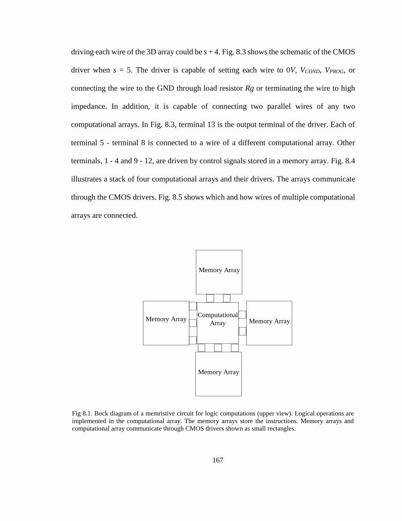
167
driving each wire of the 3D array could be s + 4. Fig. 8.3 shows the schematic of the CMOS
driver when s = 5. The driver is capable of setting each wire to 0V, VCOND, VPROG, or
connecting the wire to the GND through load resistor Rg or terminating the wire to high
impedance. In addition, it is capable of connecting two parallel wires of any two
computational arrays. In Fig. 8.3, terminal 13 is the output terminal of the driver. Each of
terminal 5 - terminal 8 is connected to a wire of a different computational array. Other
terminals, 1 - 4 and 9 - 12, are driven by control signals stored in a memory array. Fig. 8.4
illustrates a stack of four computational arrays and their drivers. The arrays communicate
through the CMOS drivers. Fig. 8.5 shows which and how wires of multiple computational
arrays are connected.
Memory ArrayComputational
Array
Memory Array
Memory Array
Memory Array
Fig 8.1. Bock diagram of a memristive circuit for logic computations (upper view). Logical operations are
implemented in the computational array. The memory arrays store the instructions. Memory arrays and
computational array communicate through CMOS drivers shown as small rectangles.

168
Fig. 8.2. Block diagram of a 3D memristive array (top side view).
0V VCOND
VPROG Rg
1
2
3
4
5
7
8
6
9
10
12
13
11
(a) (b)
Fig. 8.3. (a) Schematic of a single CMOS driver in Fig. 8.2. (b) Driver’s circuitry.
Mux1
Mux2
Vias
Pad
Swiching
Driver
Toward a computational array
Toward a memory array

169
Fig. 8.4. Schematic of four stacked computational arrays and their CMOS drivers (bird view). Outputs of the
stacked computational arrays are beneath the memory arras. The memory arrays are not shown in this figure.
Fig. 8.5a shows terminals 5-8 and 13 of four stacked CMOS drivers (bird view) and
how the black output wires of the drivers communicate through the terminals. The black
parallel wires are belong to four stacked computational arrays. Fig. 8.5b shows terminals
5-8 and 13 of four stacked CMOS drivers (side view) when only the connections of the
most bottom driver are illustrated. Fig. 8.5c shows all the connections of Fig. 8.5b. The
three-dimensional circuit shown in Fig. 8.4 enables parallel computing where all
computational arrays can process simultaneously. Note that the driver shown in Fig. 8.2
can be modified to allow performing hybrid volistor and stateful logic gates as shown in
Fig. 8.6. The complexity of the driver is increased by one additional control signal (14),
...
...
4
4
CMOS
Driver
...
Instructions and
control signals

170
which allows for selecting between volistor and stateful logic operations. The total number
of transistors used in this driver is s + 19.
3
4
13 5 6 7 8
Wire
Four stacked
CMOS drivers
(a) (b)
(c)
Fig. 8.5. (a) Schematic of driver’s interconnections with computational arrays shown in Fig. 8.2 (bird view)
(b) Four stacked CMOS drivers (Bird view). (c) Schematic of four stacked CMOS drivers which shows
how four wires of four stacked computational arrays communicate through the drivers (side view).

171
0V
Rg
1
2
3
12
5
7
8
6
9
10
11
13
inputVCOND
¬ inputVPROG
14
14
Fig. 8.6. CMOS driver for logic computing with hybrid volistor and stateful logic operations.

172
Chapter 9
Summary, Conclusion, Achievements and Future Work
9.1 SUMMARY AND CONCLUSION
The research reported in this dissertation focused on one particular problem: How to
improve logic computations based on memristor technology in non von-Neumann
architectures. To proceed with this goal, multiple design choices for logic computations
were studied. We found that the use of rectifying memristors (over non-rectifying
memristors) is desirable for logic computations due to the power and area saving benefits,
as described in Section 2.5. Using the rectifying memristors with a particular bias scheme
produce converse non-implication gates which forms a functionally complete set of logic
gates with TRUE operation. The ISD notation for logic analysis and synthesis with IMPLY
gates is extended to EISD to enable logic synthesis with IMPLY and INH gates.
Capitalizing on the characteristics of rectifying memristors, a particular realization of logic
gates called volistors were introduced. Volistors allow voltages to be used directly as
inputs. This eliminates the need for a reference resistor to read out the inputs in the first
logic level and thus eliminates the most power-hungry circuit element in most of the
stateful gates. Using multiple crossbars in a network provides parallelization, leading to
pipelined architectures. Several different first-level volistor operations can be computed in
separate crossbars at the same time, speeding up what is typically the most complex level
of implementing Boolean functions. Subsequent logic levels can be accomplished in
connected crossbars in an approach that uses mixed input gates and stateful NOR. This

173
hybrid approach with volistors and stateful INH NOR can be used to compute logic faster,
with less power than a solely stateful approach.
A programmable diode logic gate is another logic computing style proposed in this
dissertation. The programmable diode gates also rely on rectifying memristors to allow
voltages to be used directly as inputs. A memristive PLA-like circuit called mPLD-XOR
was proposed using the programmable diode gates. The mPLD-XOR is designed to
implement multi-output functions well suited for XOR of sums or products structure such
as arithmetic and communication functions. The input levels of such functions are realized
with programmable diode gates and the output levels with CMOS modulo-two counters.
The number of computational steps for calculating a multi-output function equals the
maximum number of inputs to any output XOR gate when the number of modulo-two
counters is large enough to calculate the outputs simultaneously. A 3-bit adder and 3-bit
multiplier were implemented using the mPLD-XOR, and the size and performance of each
circuit were compared with the implementation of stateful gates. The size of ReRAM and
the number of clock cycles for realizing the adder in mPLD-XOR approach to the stateful
approach are 280:957 and 8:29 respectively. For the 3-bit multiplier, these ratios are
564:4290 and 12:65. Adding feedback circuits to mPLD-XOR, as shown in Fig. 5.11,
allows the implementation of a multilevel XOR logic network with any combination of
sums, products, XORs, and literals at the input of any XOR gate. The mPLD-XOR with
feedback circuit has the potential to decrease the number of computational steps and the
size of ReRAM. In realizing the 3-bit multiplier, the size of ReRAM and the number of
computational steps in mPLD-XOR with a feedback circuit to the mPLD-XOR without a

174
feedback circuit are 564:1400 and 12:40, respectively. A 16-bit adder is also implemented
in the mPLD-XOR and Xilinx Artix-7 FPGA XC7A100T. The power consumption of the
mPLD-XOR is smaller than the Artix-7 FPGA but performs slower. In addition, the size
and delay comparisons of an N-bit adder realized with multiple approaches show that the
mPLD-XOR adder is more area-delay efficient.
A new approach for realizing a two-input XNOR logic gate was proposed. The
realization of a multi-input XNOR gate using the 2-input volistor XNOR gate was also
described. Volistor XNOR gates enable a resistive computation of arithmetic and
communication circuits that use multi-input XNOR gates. The computational delay of the
N-input XNOR gate is 2N-1. Comparisons were made for power, area, and delay evaluation
demonstrating the benefits of the volistor XNOR gate.
New implementation approach for multiple volistor gates in crossbar arrays was
proposed. In addition, the constraints for realizing volistor gates were described. These
constraints determine the size of the computational array and the voltage levels required
for implementing the gates. An implementation example of programmable mPLA based
on hybrid volistor and memristive diode gates was explained. In the hybrid mPLA, the
delay is only two clock cycles and the size of the memory array is smaller than those of
other mPLA circuits.
Example of a three-dimensional memristive circuit was shown. The interface between
CMOS and memristive circuits were designed. The circuit allows for parallel computing.
In conclusion, the problem of communication and memory access in von Neumann
architectures potentially can be solved using memristive technology. Memristors can be
175
used simultaneously as storage and processing elements enabling in-memory computing
architectures. In this dissertation, multiple approaches for logic computations were
proposed to increase computational efficiency. Examples were presented demonstrating
the benefits of the proposed approaches.
In future work, the three-dimensional circuit structure proposed in Chapter 8 will be
investigated for logic computations. The computation efficiency and energy dissipation
will be evaluated, and the possibility of replicating the circuit and connecting multiple such
circuits will be studied.
9.2 ACHIEVEMENTS AND PUBLICATIONS
This dissertation shows novel logic styles (techniques for logic computations) based on
memristors. These techniques can be effectively used in FPGA-like circuits to decrease the
computational delays (compared with fully stateful logic approaches). These new
techniques are capable of decreasing the power dissipation by eliminating the frequently
need for the programming step in stateful logic approaches. The programming step is
usually the most power-hungry step in stateful logic approaches. The proposed techniques
in this dissertation can be used together to implement two-level logic functions (SOP and
POS) in just one clock cycle. The new approaches enable in-memory computing in non
von-Neumann architectures. A complete example of hybrid CMOS-memristive circuit
including control and datapath are shown. The circuit (mPLD-XOR) is capable of realizing
generalized ESOP functions. The mPLD-XOR is designed with a very simple control and
datapath compared to other proposed hybrid CMOS-memristive circuit structures [78]. The
main contributions in this dissertation are published in journal papers as mentioned below.

176
[1] Aljafar, M., Long, P., & Perkowski, M. (2016). Memristor-Based Volistor Gates
Compute Logic with Low Power Consumption. BioNanoScience, 6(3), 214-234.
[2] Aljafar, M. J., Perkowski, M. A., Acken, J. M. & Tan, R. A Time-Efficient CMOS-
Memristive Programmable Circuit Realizing Logic Functions in Generalized AND-
XOR Structures. IEEE Transactions on Very Large Scale Integration (VLSI)
Systems, PP (99), 1-14.
[3] Aljafar, M. J., Perkowski, M. A. & Acken, J. M. Memristor-based Multi-Input
Volistor XNOR Gate for Arithmetic Circuits. Submitted for journal publication.
[4] Aljafar, M. J., Perkowski, M. A. & Acken, J. M. Volistor Logic Operations in
Crossbar Array of Rectifying Memristors. Submitted for journal publication.
177
TERMINAL REFERENCES
[1] International Technology Roadmap for Semiconductors (ITRS). Emerging Research
Devices. ITRS technical report
<http://www.itrs.net/Links/2009ITRS/2009Chapters_2009Tables/2009_ERD.pdf>
(2009).
[2] Strukov, D. B., Snider, G. S., Stewart, D. R., & Williams, R. S. (2008). The missing
memristor found. Nature, 453(7191), 80.
[3] Chua, L. (1971). Memristor-the missing circuit element. IEEE Transactions on circuit
theory, 18(5), 507-519.
[4] Chua, L. O., & Kang, S. M. (1976). Memristive devices and systems. Proceedings of
the IEEE, 64(2), 209-223.
[5] Joglekar, Y. N., & Wolf, S. J. (2009). The elusive memristor: properties of basic
electrical circuits. European Journal of Physics, 30(4), 661.
[6] Biolek, Z., Biolek, D., & Biolkova, V. (2009). SPICE Model of Memristor with
Nonlinear Dopant Drift. Radioengineering, 18(2).
[7] Prodromakis, T., Peh, B. P., Papavassiliou, C., & Toumazou, C. (2011). A versatile
memristor model with nonlinear dopant kinetics. IEEE transactions on electron
devices, 58(9), 3099-3105.
[8] Yang, J. J., Pickett, M. D., Li, X., Ohlberg, D. A., Stewart, D. R., & Williams, R. S.
(2008). Memristive switching mechanism for metal/oxide/metal nanodevices. Nature
nanotechnology, 3(7), 429-433.
[9] Strukov, D. B., & Williams, R. S. (2009). Exponential ionic drift: fast switching and
low volatility of thin-film memristors. Applied Physics A: Materials Science &
Processing, 94(3), 515-519.
[10] Lehtonen, E., & Laiho, M. (2010, February). CNN using memristors for
neighborhood connections. In Cellular Nanoscale Networks and Their Applications
(CNNA), 2010 12th International Workshop on (pp. 1-4). IEEE.
[11] Lehtonen, E., Poikonen, J., Laiho, M., & Lu, W. (2011, May). Time-dependency
of the threshold voltage in memristive devices. In Circuits and Systems (ISCAS), 2011
IEEE International Symposium on (pp. 2245-2248). IEEE.
[12] Pickett, M. D., Strukov, D. B., Borghetti, J. L., Yang, J. J., Snider, G. S., Stewart,
D. R., & Williams, R. S. (2009). Switching dynamics in titanium dioxide memristive
devices. Journal of Applied Physics, 106(7), 074508.
[13] Simmons, J. G. (1963). Generalized formula for the electric tunnel effect between
similar electrodes separated by a thin insulating film. Journal of applied physics, 34(6),
1793-1803.
[14] Kvatinsky, S., Friedman, E. G., Kolodny, A., & Weiser, U. C. (2013). TEAM:
Threshold adaptive memristor model. IEEE Transactions on Circuits and Systems I:
Regular Papers, 60(1), 211-221.
[15] Kim, K. H., Gaba, S., Wheeler, D., Cruz-Albrecht, J. M., Hussain, T., Srinivasa,
N., & Lu, W. (2011). A functional hybrid memristor crossbar-array/CMOS system for
data storage and neuromorphic applications. Nano letters, 12(1), 389-395.

178
[16] Likharev, K. K., & Strukov, D. B. (2006). CMOL: Devices, circuits, and
architectures. In Introducing Molecular Electronics (pp. 447-477). Springer Berlin
Heidelberg.
[17] Strukov, D. B., & Williams, R. S. (2009). Four-dimensional address topology for
circuits with stacked multilayer crossbar arrays. Proceedings of the National Academy
of Sciences, 106(48), 20155-20158.
[18] Snider, G. (2005). Computing with hysteretic resistor crossbars. Applied Physics
A: Materials Science & Processing, 80(6), 1165-1172.
[19] Kuekes, P. (2008, November). Material implication: Digital logic with memristors.
In Memristor and memristive systems symposium (Vol. 21).
[20] Borghetti, J., Snider, G. S., Kuekes, P. J., Yang, J. J., Stewart, D. R., & Williams,
R. S. (2010). ‘Memristive’switches enable ‘stateful’logic operations via material
implication. Nature, 464(7290), 873-876.
[21] Pershin, Y. V., & Di Ventra, M. (2010). Practical approach to programmable analog
circuits with memristors. IEEE Transactions on Circuits and Systems I: Regular
Papers, 57(8), 1857-1864.
[22] Linn, E., Rosezin, R., Kügeler, C., & Waser, R. (2010). Complementary resistive
switches for passive nanocrossbar memories. Nature materials, 9(5), 403.
[23] Shin, S., Kim, K., & Kang, S. M. (2011). Reconfigurable stateful NOR gate for
large-scale logic-array integrations. IEEE Transactions on Circuits and Systems II:
Express Briefs, 58(7), 442-446.
[24] Klimo, M., & Such, O. (2011). Memristors can implement fuzzy logic. arXiv
preprint arXiv:1110.2074.
[25] Lehtonen, E., Poikonen, J. H., & Laiho, M. (2012, August). Applications and
limitations of memristive implication logic. In Cellular Nanoscale Networks and Their
Applications (CNNA), 2012 13th International Workshop on (pp. 1-6). IEEE.
[26] Rose, G. S., Rajendran, J., Manem, H., Karri, R., & Pino, R. E. (2012). Leveraging
memristive systems in the construction of digital logic circuits. Proceedings of the
IEEE, 100(6), 2033-2049.
[27] Kvatinsky, S., Wald, N., Satat, G., Kolodny, A., Weiser, U. C., & Friedman, E. G.
(2012, August). MRL—memristor ratioed logic. In Cellular Nanoscale Networks and
Their Applications (CNNA), 2012 13th International Workshop on (pp. 1-6). IEEE.
[28] Kvatinsky, S., Belousov, D., Liman, S., Satat, G., Wald, N., Friedman, E. G., &
Weiser, U. C. (2014). MAGIC—Memristor-aided logic. IEEE Transactions on
Circuits and Systems II: Express Briefs, 61(11), 895-899.
[29] Aljafar, M., Long, P., & Perkowski, M. (2016). Memristor-Based Volistor Gates
Compute Logic with Low Power Consumption. BioNanoScience, 6(3), 214-234.
[30] Gaba, S., Sheridan, P., Zhou, J., Choi, S., & Lu, W. (2013). Stochastic memristive
devices for computing and neuromorphic applications. Nanoscale, 5(13), 5872-5878.
[31] Kim, H., Sah, M. P., Yang, C., & Chua, L. O. (2010, February). Memristor-based
multilevel memory. In Cellular nanoscale networks and their applications (CNNA),
2010 12th international workshop on (pp. 1-6). IEEE.
[32] Bürger, J., & Teuscher, C. (2013, July). Variation-tolerant computing with
memristive reservoirs. In Proceedings of the 2013 IEEE/ACM International
Symposium on Nanoscale Architectures (pp. 1-6). IEEE Press.

179
[33] Gao, L., Alibart, F., & Strukov, D. B. (2013). Programmable CMOS/memristor
threshold logic. IEEE Transactions on Nanotechnology, 12(2), 115-119.
[34] Maan, A. K., Jayadevi, D. A., & James, A. P. (2017). A survey of memristive
threshold logic circuits. IEEE transactions on neural networks and learning
systems, 28(8), 1734-1746.
[35] Strukov, D. B., & Likharev, K. K. (2005). CMOL FPGA: a reconfigurable
architecture for hybrid digital circuits with two-terminal
nanodevices. Nanotechnology, 16(6), 888.
[36] Xia, Q., Robinett, W., Cumbie, M. W., Banerjee, N., Cardinali, T. J., Yang, J. J.,
& Snider, G. S. (2009). Memristor− CMOS hybrid integrated circuits for
reconfigurable logic. Nano letters, 9(10), 3640-3645.
[37] Aljafar, M. J., Perkowski, M. A., Acken, J. M. & Tan, R. A Time-Efficient
CMOS-Memristive Programmable Circuit Realizing Logic Functions in Generalized
AND-XOR Structures. IEEE Transactions on Very Large Scale Integration (VLSI)
Systems, PP (99), 1-14.
[38] Govoreanu, B., Kar, G. S., Chen, Y. Y., Paraschiv, V., Kubicek, S., Fantini, A., &
Jossart, N. (2011, December). 10× 10nm 2 Hf/HfO x crossbar resistive RAM with
excellent performance, reliability and low-energy operation. In Electron Devices
Meeting (IEDM), 2011 IEEE International (pp. 31-6). IEEE.
[39] Li, K. S., Ho, C., Lee, M. T., Chen, M. C., Hsu, C. L., Lu, J. M., & Lin, C. Y. (2014,
June). Utilizing Sub-5 nm sidewall electrode technology for atomic-scale resistive
memory fabrication. In VLSI Technology (VLSI-Technology): Digest of Technical
Papers, 2014 Symposium on (pp. 1-2). IEEE.
[40] Lee, M. J., Lee, C. B., Lee, D., Lee, S. R., Chang, M., Hur, J. H., & Chung, U. I.
(2011). A fast, high-endurance and scalable non-volatile memory device made from
asymmetric Ta2O5-x/TaO2-x bilayer structures. Nature materials, 10(8), 625.
[41] Wei, Z., Takagi, T., Kanzawa, Y., Katoh, Y., Ninomiya, T., Kawai, K., &
Miyanaga, R. (2012, May). Retention model for high-density ReRAM. In Memory
Workshop (IMW), 2012 4th IEEE International (pp. 1-4). IEEE.
[42] Torrezan, A. C., Strachan, J. P., Medeiros-Ribeiro, G., & Williams, R. S. (2011).
Sub-nanosecond switching of a tantalum oxide memristor. Nanotechnology, 22(48),
485203.
[43] Borghetti, J., Li, Z., Straznicky, J., Li, X., Ohlberg, D. A., Wu, W., & Williams, R.
S. (2009). A hybrid nanomemristor/transistor logic circuit capable of self-
programming. Proceedings of the National Academy of Sciences, 106(6), 1699-1703.
[44] Laiho, M., & Lehtonen, E. (2010, May). Cellular nanoscale network cell with
memristors for local implication logic and synapses. In Circuits and Systems (ISCAS),
Proceedings of 2010 IEEE International Symposium on (pp. 2051-2054). IEEE.
[45] Kim, K. H., Hyun Jo, S., Gaba, S., & Lu, W. (2010). Nanoscale resistive memory
with intrinsic diode characteristics and long endurance. Applied Physics Letters, 96(5),
053106.
[46] Kim, K. M., Zhang, J., Graves, C., Yang, J. J., Choi, B. J., Hwang, C. S., &
Williams, R. S. (2016). Low-Power, Rectifying, and Forming-Free Memristor with an
Asymmetric Programing Voltage for a High-Density Crossbar Application. Nano
letters, 16(11), 6724-6732.

180
[47] Lehtonen, E., Tissari, J., Poikonen, J., Laiho, M., & Koskinen, L. (2014). A cellular
computing architecture for parallel memristive stateful logic. Microelectronics
Journal, 45(11), 1438-1449.
[48] Lehtonen, E., Poikonen, J. H., & Laiho, M. (2014). Memristive stateful logic.
In Memristor Networks (pp. 603-623). Springer International Publishing.
[49] Raghuvanshi, A., & Perkowski, M. (2014, November). Logic synthesis and a
generalized notation for memristor-realized material implication gates. In Proceedings
of the 2014 IEEE/ACM International Conference on Computer-Aided Design (pp. 470-
477). IEEE Press.
[50] Xu, C., Dong, X., Jouppi, N. P., & Xie, Y. (2011, March). Design implications of
memristor-based RRAM cross-point structures. In Design, Automation & Test in
Europe Conference & Exhibition (DATE), 2011 (pp. 1-6). IEEE.
[51] Chen, Y. C., Chen, C. F., Chen, C. T., Yu, J. Y., Wu, S., Lung, S. L., & Lu, C. Y.
(2003, December). An access-transistor-free (0T/1R) non-volatile resistance random
access memory (RRAM) using a novel threshold switching, rectifying chalcogenide
device. In Electron Devices Meeting, 2003. IEDM'03 Technical Digest. IEEE
International (pp. 37-4). IEEE.
[52] Flocke, A., & Noll, T. G. (2007, September). Fundamental analysis of resistive
nano-crossbars for the use in hybrid Nano/CMOS-memory. In Solid State Circuits
Conference, 2007. ESSCIRC 2007. 33rd European (pp. 328-331). IEEE.
[53] Zidan, M. A., Eltawil, A. M., Kurdahi, F., Fahmy, H. A., & Salama, K. N. (2014).
Memristor multiport readout: A closed-form solution for sneak paths. IEEE
Transactions on Nanotechnology, 13(2), 274-282.
[54] Gao, Y., Kavehei, O., Al-Sarawi, S. F., Ranasinghe, D. C., & Abbott, D. (2016).
Read operation performance of large selectorless cross-point array with rectifying
memristive device. INTEGRATION, the VLSI journal, 54, 56-64.
[55] Liang, J., & Wong, H. S. P. (2010). Cross-point memory array without cell
selectors—Device characteristics and data storage pattern dependencies. IEEE
Transactions on Electron Devices, 57(10), 2531-2538.
[56] Chen, A. (2013). A comprehensive crossbar array model with solutions for line
resistance and nonlinear device characteristics. IEEE Transactions on Electron
Devices, 60(4), 1318-1326.
[57] Youn, Y., Kim, K., Sim, J. Y., Park, H. J., & Kim, B. (2017). Investigation on the
Worst Read Scenario of a ReRAM Crossbar Array. IEEE Transactions on Very Large
Scale Integration (VLSI) Systems.
[58] Lehtonen, E., Poikonen, J. H., & Laiho, M. (2010). Two memristors suffice to
compute all Boolean functions. Electronics letters, 46(3), 239-240.
[59] Gimpel, J. F. (1967). The minimization of TANT networks. IEEE Transactions on
Electronic Computers, (1), 18-38.
[60] Perkowski, M., Fiszer, R., Kerntopf, P., & Lukac, M. (2012, August). An approach
to synthesis of reversible circuits for partially specified functions. In Nanotechnology
(IEEE-NANO), 2012 12th IEEE Conference on (pp. 1-6). IEEE.
[61] Jo, S. H., Kim, K. H., & Lu, W. (2009). High-density crossbar arrays based on a Si
memristive system. Nano letters, 9(2), 870-874.
181
[62] Shin, S., Kim, K., & Kang, S. M. (2012). Memristive XOR for resistive
multiplier. Electronics letters, 48(2), 78-80.
[63] Wilkinson, R. H. (1963). A method of generating functions of several variables
using analog diode logic. IEEE Transactions on Electronic Computers, (2), 112-129.
[64] Debnath, D., & Sasao, T. (1997, January). An optimization of AND-OR-EXOR
three-level networks. In Design Automation Conference, 1997. Proceedings of the
ASP-DAC'97 Asia and South Pacific (pp. 545-550). IEEE.
[65] Debnath, D., & Sasao, T. (1998, February). A heuristic algorithm to design AND-
OR-EXOR three-level networks. In Design Automation Conference 1998. Proceedings
of the ASP-DAC'98. Asia and South Pacific (pp. 69-74). IEEE.
[66] Lehtonen, E., Poikonen, J., & Laiho, M. (2012, May). Implication logic synthesis
methods for memristors. In Circuits and Systems (ISCAS), 2012 IEEE International
Symposium on (pp. 2441-2444). IEEE.
[67] Akinaga, H., & Shima, H. (2010). Resistive random access memory (ReRAM)
based on metal oxides. Proceedings of the IEEE, 98(12), 2237-2251.
[68] Sasao, T. (1993). EXMIN2: a simplification algorithm for exclusive-OR-sum-of-
products expressions for multiple-valued-input two-valued-output functions. IEEE
Transactions on Computer-Aided Design of Integrated Circuits and Systems, 12(5),
621-632.
[69] Sasao, T., & Besslich, P. (1990). On the complexity of mod-2l sum PLA's. IEEE
Transactions on Computers, 39(2), 262-266.
[70] Muroga, S. (1979). Logic design and switching theory.
[71] Weste, N. H., & Eshraghian, K. (1985). Principles of CMOS VLSI design (Vol.
188). New York: Addison-Wesley.
[72] James, A. P., Francis, L. R. V., & Kumar, D. S. (2014). Resistive threshold
logic. IEEE Transactions on Very Large Scale Integration (VLSI) Systems, 22(1), 190-
195.
[73] Lehtonen, E., Poikonen, J. H., Tissari, J., Laiho, M., & Koskinen, L. (2015).
Recursive algorithms in memristive logic arrays. IEEE Journal on Emerging and
Selected Topics in Circuits and Systems, 5(2), 279-292.
[74] Talati, N., Gupta, S., Mane, P., & Kvatinsky, S. (2016). Logic design within
memristive memories using memristor-aided loGIC (MAGIC). IEEE Transactions on
Nanotechnology, 15(4), 635-650.
[75] Xie, L., Du Nguyen, H. A., Taouil, M., Hamdioui, S., & Bertels, K. (2015,
October). Fast Boolean logic mapped on memristor crossbar. In Computer Design
(ICCD), 2015 33rd IEEE International Conference on (pp. 335-342). IEEE.
[76] Kvatinsky, S., Satat, G., Wald, N., Friedman, E. G., Kolodny, A., & Weiser, U. C.
(2014). Memristor-based material implication (IMPLY) logic: Design principles and
methodologies. IEEE Transactions on Very Large Scale Integration (VLSI)
Systems, 22(10), 2054-2066.
[77] Du Nguyen, H. A., Xie, L., Taouil, M., Nane, R., Hamdioui, S., & Bertels, K.
(2017). On the Implementation of Computation-in-Memory Parallel Adder. IEEE
Transactions on Very Large Scale Integration (VLSI) Systems.
[78] Rahman, K. C., Hammerstrom, D., Li, Y., Castagnaro, H., & Perkowski, M. A.
(2016). Methodology and design of a massively parallel memristive stateful IMPLY

182
logic-based reconfigurable architecture. IEEE Transactions on Nanotechnology, 15(4),
675-686.
[79] Chen, Y., Jung, G. Y., Ohlberg, D. A., Li, X., Stewart, D. R., Jeppesen, J. O., ... &
Williams, R. S. (2003). Nanoscale molecular-switch crossbar
circuits. Nanotechnology, 14(4), 462.
[80] DeHon, A. (2003). Array-based architecture for FET-based, nanoscale
electronics. IEEE Transactions on Nanotechnology, 2(1), 23-32.
[81] Zhong, Z., Wang, D., Cui, Y., Bockrath, M. W., & Lieber, C. M. (2003). Nanowire
crossbar arrays as address decoders for integrated nanosystems. Science, 302(5649),
1377-1379.
[82] Adam, G. C., Hoskins, B. D., Prezioso, M., & Strukov, D. B. (2016). Optimized
stateful material implication logic for three-dimensional data manipulation. Nano
Research, 9(12), 3914-3923.
[83] Yang, J. J., Strukov, D. B., & Stewart, D. R. (2013). Memristive devices for
computing. Nature nanotechnology, 8(1), 13.
[84] Eshraghian, K., Cho, K. R., Kavehei, O., Kang, S. K., Abbott, D., & Kang, S. M.
S. (2011). Memristor MOS content addressable memory (MCAM): Hybrid architecture
for future high performance search engines. IEEE Transactions on Very Large Scale
Integration (VLSI) Systems, 19(8), 1407-1417.
[85] Di Ventra, M., Pershin, Y. V., & Chua, L. O. (2009). Circuit elements with
memory: memristors, memcapacitors, and meminductors. Proceedings of the
IEEE, 97(10), 1717-1724.
[86] Jo, S. H., Chang, T., Ebong, I., Bhadviya, B. B., Mazumder, P., & Lu, W. (2010).
Nanoscale memristor device as synapse in neuromorphic systems. Nano letters, 10(4),
1297-1301.
[87] Rosezin, R., Linn, E., Kugeler, C., Bruchhaus, R., & Waser, R. (2011). Crossbar
logic using bipolar and complementary resistive switches. IEEE Electron Device
Letters, 32(6), 710-712.
[88] Kim, K., Shin, S., & Kang, S. M. (2011). Field programmable stateful logic
array. IEEE Transactions on Computer-Aided Design of Integrated Circuits and
Systems, 30(12), 1800-1813.
[89] Lebdeh, M. A., Abunahla, H., Mohammad, B., & Al-Qutayri, M. (2017). An
Efficient Heterogeneous Memristive xnor for In-Memory Computing. IEEE
Transactions on Circuits and Systems I: Regular Papers, 64(9), 2427-2437.
[90] Levy, Y., Bruck, J., Cassuto, Y., Friedman, E. G., Kolodny, A., Yaakobi, E., &
Kvatinsky, S. (2014). Logic operations in memory using a memristive Akers
array. Microelectronics Journal, 45(11), 1429-1437.
[91] Papandroulidakis, G., Vourkas, I., Vasileiadis, N., & Sirakoulis, G. C. (2014).
Boolean logic operations and computing circuits based on memristors. IEEE
Transactions on Circuits and Systems II: Express Briefs, 61(12), 972-976.
[92] Knag, P., Lu, W., & Zhang, Z. (2014). A native stochastic computing architecture
enabled by memristors. IEEE Transactions on Nanotechnology, 13(2), 283-293.
183
[93] Naous, R., & Salama, K. N. (2016, August). Approximate computing with
stochastic memristors. In CNNA 2016; 15th International Workshop on Cellular
Nanoscale Networks and their Applications; Proceedings of (pp. 1-2). VDE.
[94] Guckert, L., & Swartzlander, E. E. (2017). MAD gates—memristor logic design
using driver circuitry. IEEE Transactions on Circuits and Systems II: Express
Briefs, 64(2), 171-175.
[95] Luo, Y., Collier, C. P., Jeppesen, J. O., Nielsen, K. A., DeIonno, E., Ho, G., ... &
Heath, J. R. (2002). Two‐Dimensional Molecular Electronics
Circuits. ChemPhysChem, 3(6), 519-525.
[96] Thangkhiew, P. L., Gharpinde, R., & Datta, K. (2018). Efficient Mapping of
Boolean Functions to Memristor Crossbar Using MAGIC NOR Gates. IEEE
Transactions on Circuits and Systems I: Regular Papers.
[97] Wang, X., Li, S., & Zeng, Z. (2018). Configurable Logic Operations Using Hybrid
CRS-CMOS Cells. IEEE Transactions on Very Large Scale Integration (VLSI)
Systems.
[98] Lee, K. H., Lee, S. J., Kim, S. M., & Cho, K. (2013). Memristor-Based
Programmable Logic Array (PLA) and Analysis as Memristive Networks. Journal of
nanoscience and nanotechnology, 13(5), 3265-3269.
[99] Sasao, T. (1993). FPGA design by generalized functional decomposition. In Logic
synthesis and optimization (pp. 233-258). Springer, Boston, MA.
[100] Zhou, Y., Li, Y., Xu, L., Zhong, S., Xu, R., & Miao, X. (2016). A hybrid memristor‐
CMOS XOR gate for nonvolatile logic computation. physica status solidi (a), 213(4),
1050-1054.
[101] Singh, A. (2017, May). Memristor based XNOR for high speed area efficient 1-bit
full adder. In Computing, Communication and Automation (ICCCA), 2017
International Conference on (pp. 1549-1553). IEEE.

184
APPENDIX Power Properties
Property 1. When S1 > 0, the power consumption in a target memristor during VL operation can be
approximated as shown in (3.3).
𝑃𝑇𝑉𝐿 ≈ 4 × 𝑃𝑆0
𝑉𝐿 (3.3)
Proof: The power consumption in a target memristor during VL operation is 𝑃𝑇𝑉𝐿 =
(𝑉𝑊−𝑣−)2
𝑅𝑂𝑃𝐸𝑁=(𝑉𝑊+𝑣
+)2
𝑅𝑂𝑃𝐸𝑁,
and the power consumption in a source memristor set to logic ‘0’ during VL operation is 𝑃𝑆0𝑉𝐿 =
𝑉𝑊2
𝑅𝑂𝑃𝐸𝑁 .
Substituting 𝑃𝑇𝑉𝐿 and 𝑃𝑆0
𝑉𝐿 in (3.3) results in
𝑃𝑇𝑉𝐿
𝑃𝑆0𝑉𝐿 =
(𝑉𝑊+𝑣+)2
𝑉𝑊2 .
Let 𝑣+ = 𝑉𝑊 + 𝜀, then
𝑃𝑇𝑉𝐿
𝑃𝑆0𝑉𝐿 = [
2𝑉𝑊 + 𝜀
𝑉𝑊]2
= [2 +𝜀
𝑉𝑊]2
The minimum and maximum values of 𝑃𝑇𝑉𝐿
𝑃𝑆0𝑉𝐿 are calculated for (S1, S0, T) = (6, 1, 1) and (1, 1, 6),
respectively. The crossbar array is simulated for these combinations obtaining 4.002 ≤𝑃𝑇𝑉𝐿
𝑃𝑆0𝑉𝐿 ≤ 4.052.
Therefore, for any combination of S1, S0, and T where S1 > 0, 𝑃𝑇𝑉𝐿 ≈ 4 × 𝑃𝑆0
𝑉𝐿 .
Property 2. When S1 > 0, the power consumption in load resistor RG can be approximated as shown in
(3.4).
𝑃𝑅𝐺 ≈ 8 × 𝑃𝑇𝑆𝐿 (3.4)
Proof: The power consumption in load resistor RG is 𝑃𝑅𝐺 =𝑊
2
𝑅𝐺, and the power consumption in a target
memristor during SL operation is 𝑃𝑇𝑆𝐿 =
(𝑊−𝑣−)2
𝑅𝑂𝑃𝐸𝑁=(𝑊+𝑣
+)2
𝑅𝑂𝑃𝐸𝑁.
Substituting 𝑃𝑅𝐺 and 𝑃𝑇𝑆𝐿 in (3.4) results in,
𝑃𝑅𝐺
𝑃𝑇𝑆𝐿 =
𝑊2
𝑅𝐺×
𝑅𝑂𝑃𝐸𝑁
(𝑊+𝑣+)2=𝑅𝑂𝑃𝐸𝑁
𝑅𝐺×
1
[𝑊+𝑣+
𝑊]2.
Let 𝑣+ = 𝑊 + 𝜀. As a result,
𝑃𝑅𝐺
𝑃𝑇𝑆𝐿 =
𝑅𝑂𝑃𝐸𝑁
𝑅𝐺×
1
[2𝑊+
𝑊]2 =
𝑅𝑂𝑃𝐸𝑁
𝑅𝐺×
1
[2+
𝑊]2.
The minimum and maximum values of 𝑃𝑅𝐺
𝑃𝑇𝑆𝐿 are calculated for (S1, S0, T) = (7, 0, 1) and (1, 0, 7),
respectively. The crossbar array is simulated for these combinations obtaining 7.542 ≤𝑃𝑅𝐺
𝑃𝑇𝑆𝐿 ≤ 7.866.
Therefore, for any combination of S1, S0, and T where S1 > 0, 𝑃𝑅𝐺 ≈ 8 × 𝑃𝑇𝑆𝐿.
𝑃𝑇𝑉𝐿 and 𝑃𝑇
𝑆𝐿 in (3.3) and (3.4) can be substituted by PT as the power consumption in a target memristor
during SL and VL operations is approximately equal to 2 nW.

185
Property 3. When S1 > 0, the power consumption in source memristors during SL operation is
significantly smaller than the total power consumption in target memristors and load resistor RG as shown in
(3.5).
𝑃𝑆𝑆𝐿
𝑃𝑆𝐿−𝑃𝑆𝑆𝐿 ≪ 1 (3.5)
Proof: The simulation results show that the power consumption in source memristors during SL operation
( 𝑃𝑆𝑆𝐿) is negligible when compared to the power consumption in target memristors and load resistor RG. The
power consumption in source memristors set to logic ‘1’ is 1000 times larger than the power consumption in
source memristors set to logic ‘0’ since
𝑃𝑆1𝑆𝐿
𝑃𝑆0𝑆𝐿 =
(𝑣+ − 𝑊)2
𝑅𝐶𝐿𝑂𝑆𝐸𝐷×
𝑅𝑂𝑃𝐸𝑁
(𝑣+ − 𝑊)2= 103
Substituting 𝑃𝑆1𝑆𝐿 = 103 × 𝑃𝑆0
𝑆𝐿 to 𝑃𝑆𝑆𝐿
𝑃𝑆𝐿−𝑃𝑆𝑆𝐿 results in
(𝑆1 × 10
3 + 𝑆0) × 𝑃𝑆0𝑆𝐿
𝑃𝑆𝐿 − 𝑃𝑆𝑆𝐿
Substituting 𝑃𝑆𝐿 − 𝑃𝑆𝑆𝐿 with T × PT + PRG or its equivalent (T + 8) × PT in
(𝑆1×10³+𝑆0)×𝑃𝑆0
𝑆𝐿
𝑃𝑆𝐿−𝑃𝑆𝑆𝐿 results in
(𝑆1×10³+𝑆0)
(𝑇+8)×𝑃𝑇
𝑃𝑆0𝑆𝐿
.
It is required to compute the minimum value of 𝑃𝑇
𝑃𝑆0𝑆𝐿 to verify
(𝑆1×10³+𝑆0)
(𝑇+8)×𝑃𝑇
𝑃𝑆0𝑆𝐿
≪ 1. The 𝑃𝑇
𝑃𝑆0𝑆𝐿 ratio is equal to
(𝑊−𝑣−)2
𝑅𝑂𝑃𝐸𝑁×
𝑅𝑂𝑃𝐸𝑁
(𝑣+−𝑊)2 or
𝑃𝑇
𝑃𝑆0𝑆𝐿 = (
2𝑊
+ 1)2
substituting 𝑣+ = 𝑊 + 𝜀. The minimum value of 𝑃𝑇
𝑃𝑆0𝑆𝐿 is obtained for (S1, S0, T) = (1, 1, 6). For this
combination, 𝑊
=21.949 and thus
(𝑆1×10³+𝑆0)
(𝑇+8)×𝑃𝑇
𝑃𝑆0𝑆𝐿
=0.036, which is considerably smaller than 1 and proves (3.5).
The immediate consequence of (3.5) is used for deriving (3.7).
Property 4. The power consumption in source memristors connected to logic ‘1’ during VL operation is
considerably smaller than the total power consumption in source memristors connected to logic ‘0’ and target
memristors as shown in (3.6).
𝑆1×𝑃𝑆1𝑉𝐿
𝑃𝑉𝐿−𝑆1×𝑃𝑆1𝑉𝐿 ≪ 1 (3.6)
Proof: The simulation results show that the power consumption in source memristors set to logic ‘1’
during VL operation is negligible when compared to the power consumption in all memristors. In other
words,
𝑆1 × 𝑃𝑆1𝑉𝐿
𝑃𝑉𝐿 − 𝑆1 × 𝑃𝑆1𝑉𝐿 =
𝑆1 × 𝑃𝑆1𝑉𝐿
𝑆0 × 𝑃𝑆0𝑉𝐿 + 𝑇 × 𝑃𝑇
≪ 1
With the substitution of (3.3),

186
𝑆1 × 𝑃𝑆1
𝑉𝐿
𝑆0 × 𝑃𝑆0𝑉𝐿 + 𝑇 × 𝑃𝑇
≈𝑆1 × 𝑃𝑆1
𝑉𝐿
𝑆0 ×𝑃𝑇4+ 𝑇 × 𝑃𝑇
=𝑆1
𝑃𝑇𝑃𝑆1𝑉𝐿 (
𝑆04+ 𝑇)
≪ 1
The minimum value of 𝑃𝑇
𝑃𝑆1𝑉𝐿 is required to verify
𝑆1×𝑃𝑆1𝑉𝐿
𝑃𝑉𝐿−𝑆1×𝑃𝑆1𝑉𝐿 ≪ 1 and obtained for the (S1, S0, T) = (1, 0, 7)
𝑃𝑇
𝑃𝑆1𝑉𝐿 =
(2𝑉𝑊 + 𝜀)2
𝑅𝑂𝑃𝐸𝑁×
𝑅𝐶𝐿𝑂𝑆𝐸𝐷(𝑣+ − 𝑉𝑊)
2= 10−3 × (
2𝑉𝑊𝜀+ 1)2
where 𝜀 = 𝑣+ − 𝑉𝑊.The minimum value of 𝑉𝑊
𝜀 is 70.929, based on our simulation results, and thus
𝑃𝑇
𝑃𝑆1𝑉𝐿 =20.409. Therefore,
𝑆1×𝑃𝑆1𝑉𝐿
𝑃𝑉𝐿−𝑆1×𝑃𝑆1𝑉𝐿 ≈0.007, which is significantly smaller than 1 and proves (3.6). The
immediate consequence of (3.6) is used for deriving 3.7).
Property 5. When S1 = 0, the power consumption in source memristors connected to logic ‘0’ during VL
operation is considerably smaller than the power consumption in target memristors as shown in (3.8).
𝑆0×𝑃𝑆0
𝑉𝐿
𝑇×𝑃𝑇𝑉𝐿 ≪ 1 (3.8)
Proof: Our simulation results show that the power consumption in memristors during VL operation
approximately equals to the power consumption in target memristors when S1= 0. Moreover, the 𝑆0×𝑃𝑆0
𝑉𝐿
𝑇×𝑃𝑇𝑉𝐿 ratio
equals
𝑆0𝑇×
𝑉𝑊2
𝑅𝐶𝐿𝑂𝑆𝐸𝐷×
𝑅𝑂𝑃𝐸𝑁( 𝑉𝑊 + 𝑣
+)2= 103(
𝑆0𝑇) ×
1
(1 +𝑣+
𝑉𝑊)2
The upper bound of 𝑃𝑆0𝑉𝐿
𝑃𝑇𝑉𝐿 is obtained for (S0, T) = (7, 1) where VW = - 75.417 μV. As a result,
𝑃𝑆0𝑉𝐿
𝑃𝑇𝑉𝐿 =1.106×10⁻⁴, which is considerably smaller than 1 and proves (3.8). Note that for a larger crossbar
array, such as 1 × 64, Equation (3.8) still holds where the upper bound of 𝑃𝑆0𝑉𝐿
𝑃𝑇𝑉𝐿, obtained for (S0, T) = (63, 1),
equals 1.229 × 101 >> 5־.