Embed Size (px)
Citation preview

NAVAL POSTGRADUATE
SCHOOL
MONTEREY, CALIFORNIA
THESIS
Approved for public release; distribution is unlimited
A THREE-PHASE HYBRID DC-AC INVERTER SYSTEM UTILIZING HYSTERESIS CONTROL
by
Terence H. White
June 2004
Thesis Advisor: Robert Ashton Second Reader: Xiaoping Yun

THIS PAGE INTENTIONALLY LEFT BLANK

i
REPORT DOCUMENTATION PAGE Form Approved OMB No. 0704-0188 Public reporting burden for this collection of information is estimated to average 1 hour per response, including the time for reviewing instruction, searching existing data sources, gathering and maintaining the data needed, and completing and reviewing the collection of information. Send comments regarding this burden estimate or any other aspect of this collection of information, including suggestions for reducing this burden, to Washington headquarters Services, Direc-torate for Information Operations and Reports, 1215 Jefferson Davis Highway, Suite 1204, Arlington, VA 22202-4302, and to the Office of Management and Budget, Paperwork Reduction Project (0704-0188) Washington DC 20503. 1. AGENCY USE ONLY (Leave blank)
2. REPORT DATE June 2004
3. REPORT TYPE AND DATES COVERED Master’s Thesis
4. TITLE AND SUBTITLE: A Three-Phase Hybrid DC-AC Inverter System Utilizing Hysteresis Control 6. AUTHOR(S) Terence White
5. FUNDING NUMBERS
7. PERFORMING ORGANIZATION NAME(S) AND ADDRESS(ES) Naval Postgraduate School Monterey, CA 93943-5000
8. PERFORMING ORGANIZATION REPORT NUMBER
9. SPONSORING /MONITORING AGENCY NAME(S) AND ADDRESS(ES)
N/A
10. SPONSORING/MONITORING AGENCY REPORT NUMBER
11. SUPPLEMENTARY NOTES The views expressed in this thesis are those of the author and do not reflect the official policy or position of the Department of Defense or the U.S. Government. 12a. DISTRIBUTION / AVAILABILITY STATEMENT Approved for public release, distribution is unlimited
12b. DISTRIBUTION CODE
13. ABSTRACT (maximum 200 words)
The naval vessels of the future will require lighter, more compact, and more versatile power electronics systems. With the advent of the DC Zonal Electrical Distribution Sys-tem, more innovative approaches to the conversion of the dc bus power to ac power for motor drives will enhance the efficiency and warfighting capability of tomorrow’s ships. This thesis explores the concept of a hybrid dc-ac power converter that combines a hys-teresis controlled inverter with a six-step bulk inverter. A six-step bulk inverter is built from discrete components and tested in simulation and hardware. The two inverters are con-nected in parallel to provide a high-fidelity current source for a three-phase load. The ad-dition of the hysteresis inverter to the bulk inverter adds a closed current loop for more robust control and improves the quality of the output load current.
15. NUMBER OF PAGES
93
14. SUBJECT TERMS Hybrid inverter, hysteresis control, inverter, parallel inverters, six-step inverter, shipboard motor drives.
16. PRICE CODE
17. SECURITY CLASSIFICATION OF REPORT
Unclassified
18. SECURITY CLASSIFICATION OF THIS PAGE
Unclassified
19. SECURITY CLASSIFICATION OF ABSTRACT
Unclassified
20. LIMITATION OF ABSTRACT
UL
NSN 7540-01-280-5500 Standard Form 298 (Rev. 2-89) Prescribed by ANSI Std. 239-18

ii
THIS PAGE INTENTIONALLY LEFT BLANK

iii
Approved for public release; distribution is unlimited
A THREE-PHASE HYBRID DC-AC INVERTER SYSTEM UTILIZING HYSTERESIS CONTROL
Terence H. White
Major, United States Marine Corps B.S., University of California, Los Angeles, 1991
Submitted in partial fulfillment of the requirements for the degree of
MASTER OF SCIENCE IN ELECTRICAL ENGINEERING
from the
NAVAL POSTGRADUATE SCHOOL June 2004
Author: Terence H. White Approved by: Robert W. Ashton
Thesis Advisor
Xiaoping Yun Second Reader John P. Powers Chairman, Department of Electrical and Computer
Engineering

iv
THIS PAGE INTENTIONALLY LEFT BLANK

v
ABSTRACT
The naval vessels of the future will require lighter, more compact, and
more versatile power electronics systems. With the advent of the DC Zonal
Electrical Distribution System, more innovative approaches to the conversion of
the dc bus power to ac power for motor drives will enhance the efficiency and
warfighting capability of tomorrow’s ships. This thesis explored the concept of a
hybrid dc-ac power converter that combines a hysteresis controlled inverter with
a six-step bulk inverter. A six-step bulk inverter was built from discrete compo-
nents and tested in simulation and hardware. The two inverters were connected
in parallel to provide a high-fidelity current source for a three-phase load. The
addition of the hysteresis inverter to the bulk inverter added a closed current loop
for more robust control and improved the quality of the output load current.

vi
THIS PAGE INTENTIONALLY LEFT BLANK
vii
TABLE OF CONTENTS
I. INTRODUCTION........................................................................................................ 1 A. RESEARCH GOALS..................................................................................... 2 B. SCOPE OF THESIS ...................................................................................... 2
II. BACKGROUND INFORMATION ............................................................................ 5 A. INVERTER BASICS...................................................................................... 5 B. HYSTERESIS CONTROL ..........................................................................10 C. HYBRID INVERTERS .................................................................................12
III. SYSTEM DESIGN AND DEVELOPMENT..........................................................17 A. OVERALL SYSTEM DESIGN ...................................................................17 B. HYSTERESIS INVERTER..........................................................................18 C. BULK INVERTER........................................................................................21 D. SYSTEM CONFIGURATION .....................................................................27
IV. THEORETICAL RESULTS....................................................................................29 A. OVERALL PERFORMANCE.....................................................................29 B. HYSTERESIS INVERTER CURRENT .....................................................30 C. BULK INVERTER CURRENT...................................................................31
V. EXPERIMENTAL RESULTS.................................................................................41 A. PRELIMINARY TESTING OF BULK INVERTER ..................................41 B. THREE-PHASE TESTING OF HYSTERESIS INVERTER...................43 C. SINGLE-PHASE PARALLEL TESTING..................................................44 D. THREE-PHASE PARALLEL TESTING...................................................45 E. ZERO-SEQUENCE CURRENT.................................................................52 F. SUMMARY OF RESULTS.........................................................................54
VI. CONCLUSION..........................................................................................................57 A. REVIEW OF RESEARCH QUESTIONS AND GOALS.........................57 B. SUMMARY OF EXPERIMENTAL RESULTS.........................................57 C. ANSWERS TO RESEARCH QUESTIONS BASED ON RESULTS...58 D. RECOMMENDATIONS FOR FURTHER DEVELOPMENT.................58
APPENDIX A. CIRCUIT WIRING DIAGRAMS .....................................................61
APPENDIX B. MATLAB SIMULATION CODE .....................................................69
LIST OF REFERENCES.....................................................................................................73
INITIAL DISTRIBUTION LIST ...........................................................................................75

viii
THIS PAGE INTENTIONALLY LEFT BLANK

ix
LIST OF FIGURES
Figure 1. Half-Bridge Inverter Circuit Topology.......................................................... 5 Figure 2. Pulse-width modulation reference and carrier signals ............................. 8 Figure 3. Typical Sine-PWM applied load voltage (From Reference 3). ................ 9 Figure 4. Hysteresis band for inverter control...........................................................11 Figure 5. Topology of series-connected hybrid inverter (from Reference 2). ......13 Figure 6. Hybrid current-source/voltage source inverter (From Reference 5). ...14 Figure 7. Overall system block diagram of hybrid inverter system. ......................18 Figure 8. Controller section of hysteresis inverter (From Reference 2). ..............19 Figure 9. Power section of hysteresis inverter (From Reference 2). ...................20 Figure 10. Block diagram of hysteresis inverter (After Reference 2). ....................20 Figure 11. System block diagram of bulk inverter controller. ...................................21 Figure 12. 60-Hz signal generator circuit (After Reference 6). ................................22 Figure 13. Phase-shifter circuit (After Reference 7). .................................................22 Figure 14. Comparator circuit to generate logic signals to switches.......................23 Figure 15. Hysteresis signal reference circuit.............................................................24 Figure 16. Amplifier circuit for square wave signal. ...................................................26 Figure 17. Gate Driver Circuit (After Reference 8). ...................................................26 Figure 18. Power section topology of hybrid inverter. ...............................................28 Figure 19. Topology of single phase of hybrid inverter. ............................................29 Figure 20. Phase A applied voltage for bulk inverter (From Reference 3).............31 Figure 21. Results of simulation of bulk inverter, phase A. ......................................34 Figure 22. Phase A, B, and C currents of the bulk inverter ( )39 VdcV∆ = . ...........36 Figure 23. Theoretical harmonic content of bulk inverter phase current................38 Figure 24. Bulk inverter phase current and voltage...................................................42 Figure 25. Phases A (top), B (middle), and C (bottom) of hysteresis inverter
operating independently with Ih = 0.1 A and ∆Vdc = 39 V. (5.0 A/div) .44 Figure 26. Phases A, B, and C in parallel operation (5.0 A/div). .............................46 Figure 27. Detailed view of phase A, B, and C currents (2.5 A/div). .......................47 Figure 28. Frequency spectrum of bulk inverter (10 dB/div, 0-2000 Hz)................48 Figure 29. Frequency spectrum of hybrid inverter (10 dBV/div, 0-2000 Hz). ........49 Figure 30. Hybrid Phase A – Bulk and Hysteresis phase currents (2A/div). ........50 Figure 31. Hybrid Phase B – Bulk and Hysteresis phase currents (2 A/div). .......51 Figure 32. Hybrid Phase C – Bulk and Hysteresis phase currents (2 A/div)........52 Figure 33. Effect of zero-sequence current on hybrid circuit (2 A/div) ....................53 Figure 34. Component Layout Diagram for Bulk Inverter Controller.......................61 Figure 35. Component Layout Diagram for Hysteresis Signal Reference
Circuit. ............................................................................................................65

x
THIS PAGE INTENTIONALLY LEFT BLANK

xi
LIST OF TABLES
Table 1. Switching algorithm for six-step bulk inverter ..........................................32 Table 2. Socket A wiring diagram .............................................................................61 Table 3. Socket B wiring diagram .............................................................................62 Table 4. Socket C wiring diagram .............................................................................62 Table 5. Socket D wiring diagram .............................................................................62 Table 6. Socket E wiring diagram .............................................................................63 Table 7. Socket F wiring diagram..............................................................................63 Table 8. Socket G wiring diagram.............................................................................63 Table 9. Socket H wiring diagram .............................................................................63 Table 10. Socket I wiring diagram...............................................................................64 Table 11. Socket J wiring diagram ..............................................................................64 Table 12. Socket K wiring diagram .............................................................................64 Table 13. Socket L wiring diagram..............................................................................64 Table 14. Socket M wiring diagram.............................................................................65 Table 15. Socket N wiring diagram .............................................................................66 Table 16. Socket P wiring diagram .............................................................................66 Table 17. Socket Q wiring diagram.............................................................................66 Table 18. Socket S wiring diagram .............................................................................67 Table 19. Socket T wiring diagram..............................................................................67 Table 20. Potentiometer (Ri) connections ..................................................................67

xii
THIS PAGE INTENTIONALLY LEFT BLANK

xiii
ACKNOWLEDGMENTS
I would like to take the opportunity to recognize the people who helped me
along the way in my research.
Thanks to all of the faculty and staff of the Naval Postgraduate School for
your expertise and dedication. It was a privilege to study at your fine institution.
I would also like to thank all of my fellow officer students who always in-
spired me with their professionalism and kept me motivated through two years of
study.
Most of all, thank you to my wife, Kathy, and my daughters, Natalie and
Chloe, for all of your love and support.

xiv
THIS PAGE INTENTIONALLY LEFT BLANK

xv
EXECUTIVE SUMMARY
This thesis continues an ongoing research effort to explore the concept of
hysteresis control to produce a high-fidelity current source inverter for use in
shipboard motor drives. The hybrid inverter system developed in this thesis ad-
dresses the fleet requirement for lighter and more compact power converters in
the proposed advanced electrical power system for future naval vessels.
A six-step bulk inverter was designed, built, and tested prior to coupling
with an existing hysteresis-controlled inverter. The two inverter elements were
connected in parallel across a three-phase wye-connected load to form a hybrid
inverter system. The hybrid inverter system capitalized on the high power capa-
bility of the bulk inverter and the closed-loop current control employed by the hys-
teresis inverter. The goal of the research was to demonstrate that the parallel
combination of the six-step bulk inverter and the hysteresis inverter could pro-
duce a high-fidelity load current. Experimental trials attempted to optimize the
system configuration to draw all of the current at the fundamental frequency from
the six-step bulk inverter and utilize the hysteresis inverter to improve the quality
of the current waveform.
The experimental testing showed that both the bulk inverter and the hys-
teresis inverter operated as designed when connected to an inductive three-
phase load with a floating neutral point. The two inverters operated well when
connected in parallel across a three-phase load. When the hysteresis inverter
was added to the bulk inverter, the total harmonic distortion of the phase current
waveform dropped from 5.5% to 3.2%. The overall current waveforms for all
three phases closely corresponded to the reference current signal and the hybrid
inverter produced a stable, sinusoidal load current. The magnitude of the phase
current was set at 5.0 A peak across a load consisting of an inductance of 9.1
mH and a resistance of 1.05 Ω.

xvi
The primary input variables were the dc bus voltage, phase shift between
the bulk and hysteresis inverter reference signals, and width of the hysteresis
band. These input variables were adjusted to optimize the hybrid inverter system
in order force the bulk inverter to produce as much of the fundamental load cur-
rent as possible . The optimal experimental results were found with the dc bus
voltage set at 30.8 V, the phase shift at 55°, and the width of the hysteresis band
at 0.1 A. Although the bulk inverter did supply most of the fundamental load cur-
rent, the hysteresis inverter was still required to produce some of the fundamen-
tal. Theoretically with further controller refinement, the hysteresis inverter should
only be needed to cancel the harmonic content of the bulk inverter.
The concept of a hybrid inverter consisting of a six-step bulk inverter and a
hysteresis controlled inverter was validated in this experiment. Follow-on re-
search including controller refinement and higher power testing can further de-
velop the hybrid inverter for potential use on shipboard motor drives.

1
I. INTRODUCTION
As naval technology continues to advance, the power electronic systems
installed in ships must become more efficient, versatile, and dependable. Inno-
vation in methods to supply power to shipboard warfighting systems will provide
the key to creating a modern and capable fleet. Electric motors perform a multi-
tude of critical functions aboard all types of ships in the United States Navy, and
they all need a clean and reliable source of power.
The proposed advanced electrical power system for future naval vessels
features the DC Zonal Electric Distribution System (DC ZEDS) to provide a more
efficient means of distributing power throughout the ships. This system will rely
heavily on dc-ac inverters that are lighter and more compact than the systems
that are available on the commercial market today. The Office of Naval Re-
search (ONR) contends that the current conventional power electronics systems
are too large and heavy, and mandates the development of unique power con-
version solutions to implement in future naval power distribution systems [1]. One
possible solution to improve the compactness and power quality of commercial
products is presented in this thesis.
The hybrid inverter system represents a unique approach to the conver-
sion of dc power to a three-phase ac supply capable of driving the various motors
aboard today’s naval vessels. The system would most likely consist of a large
commercial bulk inverter paralleled or cascaded with a high bandwidth filtering
inverter. With a simple, compact controller, the hybrid inverter developed in this
thesis can provide a high-fidelity current source that can be scaled to match an
array of applications. Utilizing the concept of hysteresis control, it can maintain a
constant current to the load despite disturbances in the dc-link voltage. With two
inverter elements connected in parallel, the hybrid inverter also provides a de-
gree of redundancy for the power source to the motor.

2
A. RESEARCH GOALS
This thesis continues previous work began in Reference 2 to develop the
concept of a hysteresis controlled inverter coupled in parallel with a six-step bulk
inverter to produce a three-phase ac source for a motor drive. In the previous
research effort, the hysteresis inverter was designed, built and tested as an inde-
pendent unit. Preliminary testing was also done to verify that a single phase of
the hysteresis inverter could work in parallel with a square-wave inverter.
The goals of the research effort are listed below.
• Design, build, and test a six-step bulk inverter capable of parallel
operation with the hysteresis inverter.
• Operate the new six-step inverter in parallel with the existing three-
phase hysteresis inverter across a wye-connected load.
• Determine if the hybrid combination of the hysteresis inverter and
the bulk inverter can produce a high-fidelity output current.
• Test the hybrid inverter under various conditions to find the optimal
operating point; produce all current at the fundamental frequency
with the bulk inverter while the hysteresis inverter cancels higher
order harmonics.
It is hoped that successful testing of the hybrid inverter would validate the
hybrid system concept and mandate continued efforts to develop the system for
shipboard use.
B. SCOPE OF THESIS
The design and construction of the six-step bulk inverter began the proc-
ess of developing a hybrid inverter system. After testing the new bulk inverter to
verify its capabilities, the existing hysteresis inverter was retested to assess its
performance before paralleling. With two operable inverter elements, the hybrid
inverter system was assembled and tested. After adjusting the bulk inverter so
that it was producing all of the fundamental current, the hybrid inverter was stud-

3
ied in detail to determine the optimal operating point and measure its perform-
ance against research goals. This thesis details the research process and con-
sists of the following chapters:
Chapter I introduces the topic and motivates the need for a novel dc-ac
power conversion system.
Chapter II builds the reader’s knowledge base on inverter theory and re-
views some of the current literature on the topic of hybrid inverters.
Chapter III describes the process of the design and development of the
components of the hybrid inverter system. The overall system level diagrams
and the details of each circuit appear here.
Chapter IV discusses the governing theory that will predict the perform-
ance of each inverter element. The predicted performance of the bulk inverter is
projected with a computer simulation.
Chapter V presents the results of each phase of the experimental testing.
The results are weighed against the predicted performance and research goals.
Chapter VI summarizes the complete results of this thesis and provides
recommendations for future research work geared to further develop the hybrid
inverter concept. Wiring diagrams, layout diagrams, MATLAB computer simula-
tion code, and relevant component data sheets can be found in the Appendices.

4
THIS PAGE INTENTIONALLY LEFT BLANK

5
II. BACKGROUND INFORMATION
This chapter familiarizes the reader with the technical concepts covered in
the thesis. The basics of inverters and the various inverter control strategies are
introduced. The chapter also includes a review of current research on hybrid
inverters.
A. INVERTER BASICS
As a critical component of most large motor drive systems, an inverter
converts a dc power source into a controlled sinusoidal input current for the mo-
tor at a desired operating frequency; the dc power is generally derived by rectify-
ing an ac generating source. The inverter uses a network of switches to alternate
the positive and negative voltage buses of the input dc source to produce the ac
voltage across the load [3]. A representation of a simple half-bridge inverter cir-
cuit is depicted in Figure 1.
S1
S2
D1
D2
RL L
+ Vdc
- Vdc
VLOAD+_
Figure 1. Half-Bridge Inverter Circuit Topology
The amplitude and frequency of the sinusoidal output of the inverter can
be controlled directly by properly timing the closure and opening of switches S1

6
and S2. The Insulated Gate Bipolar Transistor (IGBT) is an example of a type of
switch commonly used for inverters. The quality of the output waveform is de-
pendent on a number of variables that mainly include the relative switching
speed, the filtering and the bandwidth of the controller. The relative switching
speed is generally specified in number of pulses (or switchings) per half-cycle of
the output fundamental voltage or current [3]. For most loads, the ideal voltage
and current waveforms will be sinusoidal at the desired operating frequency. For
nonlinear loads, it is common to force the voltage or the current sinusoidal while
letting the load characteristics define the uncontrolled variable.
Given a fixed amount of filtering and sufficient control bandwidth, the
switching sequence including the relative rate at which the switches operate de-
termines the inverter’s output accuracy when following a reference sinusoid. As
a result, the output of an inverter at a lower relative switching frequency will not
match the desired sinusoidal pattern as closely as an inverter switching at a
higher frequency. Since non-sinusoidal waveforms are rich in harmonic content
that is not directly usable by a machine load, the total harmonic distortion (THD)
of the current should be minimized to alleviate unwanted noise from torque pul-
sations and excess heating from eddy current losses.
The load current waveform, iL(t), can be represented by a composite se-
ries of the fundamental component and the sum of the higher harmonic compo-
nents as shown below [3]:
∞
≠
= + ∑11
( ) ( ) ( ).L L Lhh
i t i t i t (2-1)
The first term (iL1) is the desired fundamental frequency component, while the
summation of the iLh terms represents harmonic content. Ideally, the harmonic
terms would be zero if a perfectly sinusoidal waveform at the fundamental fre-
quency was desired. The Root-Mean-Squared (RMS) value of the current wave-
form is given by [3]:
∞
≠
= + ∑2 21
1
.L L Lhh
I I I (2-2)

7
The actual distortion present in the current waveform due to its harmonics can be
derived from the above relations. The THD as a percentage of the total current
waveform is given by [3]:
2
1 1
%THD 100 .Lh
h L
II
∞
≠
= ×
∑ (2-3)
The objective of the inverter system is to minimize the THD in order to match the
desired reference signal as closely as possible.
Various methods can be employed to control the switches within the in-
verter to produce an ac output current. The objective of any switching control
scheme is to sequence the switches in order to match the desired reference sig-
nal. Some switching schemes are very simple, while others are quite complex
and require the use of computers and digital signal processing (DSP) equipment.
The simplest of switching methods for inverters is square-wave switching.
With this method, the inverter cycles the voltage across the load by alternating
the positive dc voltage and then the negative dc voltage at the desired output
frequency. This method simply closes the top switch when the reference signal
is positive and closes the bottom switch when the reference signal is negative.
Although easy to implement, the square-wave switching method produces an
output waveform that falls short of matching the sinusoidal reference signal. As a
result the THD of the voltage is 47.8% and 30.5% for single-phase and three-
phase, respectively [3]. The distortion in the current is based on the amount of
filtering required which can be significant since the dominate harmonic is the third
and fifth for single-phase and three-phase, respectively.
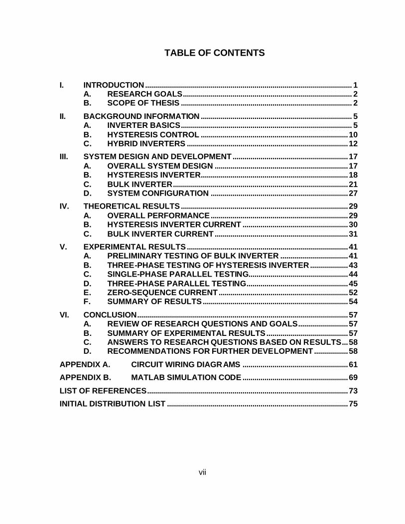
A more complex but commonly used switching scheme is called pulse-
width modulation (PWM). PWM techniques are capable of producing a good rep-
resentation of the desired waveform with only the inclusion of higher, easily filter-
able harmonics at the switching frequency. With PWM, the positive or negative
dc input source voltage is applied to the load in pulses of varying length. While
the amplitude and frequency of the pulses is fixed, the width of the individual
8
pulses is weighted by multiplying a reference waveform by a higher frequency
triangular-carrier to produce a digitized representation of the reference.
One prevalent technique of inverter control is sine-PWM. In a sine-PWM
inverter, a sinusoidal reference signal of the desired output frequency is com-
pared to a triangular modulation signal at a much higher frequency. Figure 2 il-
lustrates the two control signals and the switching scheme:
Triangular carrier signal (Vtri)Sinusoidal reference signal (Vref)
Figure 2. Pulse-width modulation reference and carrier signals
A brief description of the algorithm to control the applied voltage to the
load is shown here.
If Vref > Vtri: • Close S1 (top switch), open S2 (bottom switch). • Set VLOAD to +Vdc.
If Vref < Vtri: • Open S1 (top switch), close S2 (bottom switch) • Set VLOAD to –Vdc
The resultant applied voltage levels for a typical cycle in a sine-PWM in-
verter are depicted in Figure 3.

9
VLOADVREF
pulse width
Figure 3. Typical Sine-PWM applied load voltage (From Reference 3).
This type of inverter can produce a very high fidelity current waveform and
its use is widespread. The harmonic content of the current depends on the num-
ber of pulses applied per cycle. With a high integer count of pulses per half-
cycle, the first non-zero harmonic present in the current waveform will be signifi-
cantly separated from the fundamental and easy to filter. The order of the non-
zero harmonics present are determined by
2 1,n kr= ± (2-4)
where n represents the order of non-zero harmonics, k is the number of pulses
per cycle, and r can be any positive integer. According to this relationship, a high
value of k will make the minimum value of n a much higher order harmonic. For
example, if there were 15 pulses per cycle in a 60-Hz waveform, then the lowest
harmonic present would be the 29th harmonic ( )2 15 1⋅ − at a frequency of 1740
Hz. A relatively small low-pass filter could eliminate these components from the
current waveform.
Although a proven technique for inverter control, the sine-PWM switching
scheme and other similar schemes have a few key disadvantages. They require
the use of relatively complex hardware to implement and control, as opposed to
square-wave switching which can be controlled with a simple circuit. Also, the
high switching frequency often required can impose significant switching power
losses as the inverter needs to switch at frequencies much higher than the fun-

10
damental output frequency. The higher switching frequency necessary to pro-
duce high-fidelity waveforms can often exceed the capabilities of some power
electronic switches. Switches that are rated for very high voltage and current
have longer delays and cannot switch as fast as lower power devices. Power
electronics operating at a fixed high frequency rather than spread-spectrum may
also introduce undesirable noise into the shipboard environment which could be
easily detectable by the enemy.
B. HYSTERESIS CONTROL
Hysteresis control presents an alternative method for producing a sinusoi-
dal ac current waveform from a dc voltage source. With this method, the control-
ler maintains an output current that stays within a given tolerance of the refer-
ence waveform. The tolerance that the output stays within is called the “hystere-
sis band”. Unlike the above described PWM switching technique, the method of
hysteresis control depends on feedback from the output current to control the
inverter system. The closed-loop control method enables the inverter with hys-
teresis control to adapt instantly to changes in the output loading.
The concept of hysteresis control can be applied to a wide range of in-
verter configurations and topologies. Both single-phase and three-phase invert-
ers can be controlled by the hysteresis method as well. A common topology for
single-phase inverters is the H-bridge because it offers more controllability than
the half-bridge type. It allows the use of three output states instead of two and
requires half of the dc bus voltage to produce the same peak output voltage [3].
However, the minimum switch configuration and most popular topology for multi-
phase inverters consists of half-bridges.
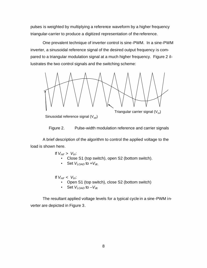
Figure 4 illustrates the fundamental concept of operation for the hystere-
sis-controlled inverter.
11
Figure 4. Hysteresis band for inverter control
The reference current, iref, represents the desired waveform for the output
load current. The top and bottom hysteresis limits form the hysteresis band,
which corresponds to the tolerance limit of the inverter controller. This discus-
sion will describe a two-level hysteresis inverter switching scheme.
The two-level inverter controller will apply the positive or negative dc bus
voltage to the load in order to keep the output current within the hysteresis band.
For example, when the output current rises above the top hysteresis limit, the
inverter controller will respond by switching the transistors to apply the negative
dc bus voltage to the load and effectively reduce the value of the output current
to bring it below the top hysteresis limit. The inverter controller will keep the
negative dc bus voltage across the load until the output current reaches the bot-
tom hysteresis limit. After the output current drops below the bottom limit, the
inverter controller will send the appropriate gating signals to the transistors to
switch them to apply the positive dc bus voltage across the load. This will bring
the output current back up above the bottom hysteresis limit and within the a l-
lowable tolerance band around the reference waveform. The controller will con-

12
tinuously repeat this cycle to maintain the output load current within the hystere-
sis band.
Unlike other high-fidelity inverter control strategies, the hysteresis control-
ler will operate at a variable switching frequency that is spread across the spec-
trum. The instantaneous switching frequency fs at any point on the current wave-
form can be predicted by [3]:
( )
,dc ref refs
h dc
V i if
LI V− | | | |
= (2-5)
where Vdc is the dc bus voltage, iref is the instantaneous voltage of reference cur-
rent signal, L is the load inductance, and Ih is the width o f the hysteresis band.
As reflected in Equation 2-5, the hysteresis inverter will switch faster at
points in the cycle where the reference current reaches its maximum and mini-
mum values and switch much slower when iref is close to zero in magnitude. A
larger load inductance will allow the inverter to switch at a lower frequency to
maintain the current within the same hysteresis band. Since fs will diverge to in-
finity if L is equal to zero, there must be some inductance present in the load for
the hysteresis-controlled inverter to work. The switching frequency is also i n-
versely proportional to Ih. The inverter will switch at higher rates overall to
achieve a higher fidelity output current within a smaller hysteresis band.
C. HYBRID INVERTERS
All of the above described switching schemes have distinct advantages
and disadvantages in their design. In general, a more complex switching
scheme such as sine-PWM will produce a more sinusoidal waveform, but it will
incur a larger power loss in the switching states as it must switch at a higher rate.
Also, a higher switching frequency may mandate the use of higher speed
switches which cannot handle as much current and voltage. In order to produce
higher power, slower switching is required given the same system components.
Conversely, the simple bulk converter arrangement only switches at a rate
equal to the actual output waveform and therefore incurs much lower overall

13
switching losses. Since the bulk converter does not switch at a very high fre-
quency, it can exploit the high power capability of the Gate Turn-Off thyristor
(GTO) or its derivatives for high voltage and current operation. However, the
output waveform of this type of inverter is too rich in harmonic content for military
propulsion loads and may not fit the requirements of many types of ancillary ac
loads. Most motor drives need a relatively smooth, sinusoidal input current to
operate properly without derating.
Recent research efforts have explored many different options in creating
hybrid inverters to capitalize on the advantages of each switching strategy. Each
effort concentrates on the common goal of producing the highest possible quality
of output waveform that can supply the maximum amount of power. The new
inverter control strategies also aim to add flexibility, reliability, and simplicity to
the process of converting dc to ac power.
One novel control strategy created a hybrid inverter from a high-fidelity
IGBT-based inverter and a low-fidelity GTO-based inverter. The complete details
of this system can be found in Reference 4. This hybrid system used a common
dc source voltage for the two series-connected three-phase inverters. The topol-
ogy of the system is depicted in Figure 5.
Figure 5. Topology of series-connected hybrid inverter (from Refer-ence 2).
The bulk inverter, with GTO switches operating at the low load frequency,
produced the majority (up to 63.7%) of the output power. The high-fidelity IGBT-

14
based inverter created the remainder of the power at the fundamental output fre-
quency and worked to offset the lower order harmonics produced by the bulk in-
verter. This hybrid inverter strategy worked well in practical experimentation as
the output from the series-connected inverters had a current THD of only 1.96%
due to the suppression of harmonics by the IGBT-based inverter.
A separate research effort, described in Reference 5, also explored the
concept of a hybrid inverter system with favorable results [5]. This experiment
placed a current-source inverter operating in a square-wave mode in parallel with
a high fidelity voltage-source inverter switching in a PWM mode at a much higher
frequency. The topology of this hybrid inverter system appears below.
3-phasemotor load
High fidelity inverter (VSI)
Low fidelity inverter (CSI)
dc source
Figure 6. Hybrid current-source/voltage source inverter (From Refer-
ence 5).
This system used the primary low fidelity inverter to generate the bulk of
the current while the secondary high fidelity inverter cancels out the low order
harmonics of the primary inverter output and augments the output at the desired
fundamental frequency. The experimental results for this system proved that it
could offer improved efficiency and responsiveness while minimizing switching
losses.
Although both of the above described research efforts proved the concept
of a square-wave mode inverter coup led with a high-fidelity inverter, they both
require the use of a complex computer system to control the switching cycles. A

15
DSP system metered the gating signals to the high fidelity PWM inverter in both
cases.
The basics of inverters were introduced in this chapter as well as some
prevalent switching schemes. A survey of current research pointed out the
emerging technology in hybrid inverter systems. This thesis will propose a dis-
tinct alternative to these hybrid inverter systems that relies only on simple dis-
crete circuits to control the inverter switches and does not require the use of
complex DSP equipment. The system proposed in this thesis will couple a sim-
ple six-step bulk inverter in parallel with a high-fidelity inverter which employs the
novel, yet simple concept of hysteresis control. The following chapter will detail
the design and development of this hybrid inverter system.

16
THIS PAGE INTENTIONALLY LEFT BLANK

17
III. SYSTEM DESIGN AND DEVELOPMENT
The hybrid inverter system brings several elements together to produce its
output current for the load. The design and construction of the complete inverter
as well as the component subsystems will be described in this chapter.
A. OVERALL SYSTEM DESIGN
The hybrid inverter system combines a relatively simple six-step bulk in-
verter and a high fidelity hysteresis controlled inverter to create a three-phase,
sinusoidal output current at the desired magnitude and frequency. The objective
of the inverter is to match a given reference current signal as closely as possible
with the output load current for each phase.
The bulk inverter utilizes a simple switching scheme to produce a three-
phase, six-step output voltage across the load at the fundamental frequency.
Since it switches at low frequency, the bulk inverter incurs only minimal switching
power losses compared to a higher fidelity inverter that switches at a much
higher rate.
The hysteresis inverter is connected in parallel with the bulk inverter and
utilizes the same dc power source. The high fidelity inverter with a closed cur-
rent-control loop serves to cancel the harmonics of the bulk inverter and make
the resultant sum of the two currents match the desired reference current across
the load. The load current for each phase complies with the following relation:
( ) ( ) ( ),L B Hi t i t i t= + (3-1)
where iB represents the bulk inverter output current and iH denotes the current
component produced by the hysteresis inverter. The hysteresis inverter monitors
the instantaneous value of the load current, iL, and adjusts the output current of
each phase to match the desired reference signal. The addition of the hysteresis
inverter enables the composite hybrid system to continuously adapt to changes
in the load current and effectively closes the current control loop. The system
level block diagram is depicted in Figure 7.
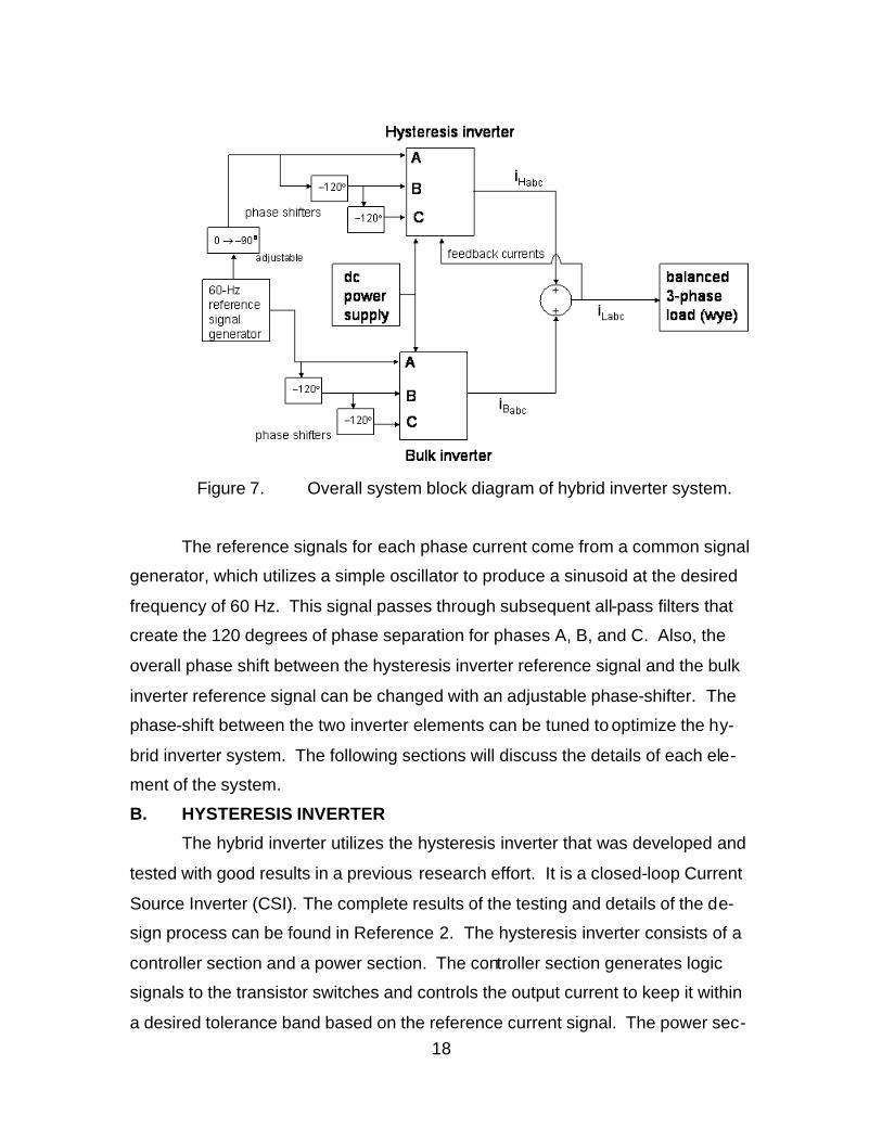
18
Figure 7. Overall system block diagram of hybrid inverter system.
The reference signals for each phase current come from a common signal
generator, which utilizes a simple oscillator to produce a sinusoid at the desired
frequency of 60 Hz. This signal passes through subsequent all-pass filters that
create the 120 degrees of phase separation for phases A, B, and C. Also, the
overall phase shift between the hysteresis inverter reference signal and the bulk
inverter reference signal can be changed with an adjustable phase-shifter. The
phase-shift between the two inverter elements can be tuned to optimize the hy-
brid inverter system. The following sections will discuss the details of each ele-
ment of the system.
B. HYSTERESIS INVERTER
The hybrid inverter utilizes the hysteresis inverter that was developed and
tested with good results in a previous research effort. It is a closed-loop Current
Source Inverter (CSI). The complete results of the testing and details of the de-
sign process can be found in Reference 2. The hysteresis inverter consists of a
controller section and a power section. The controller section generates logic
signals to the transistor switches and controls the output current to keep it within
a desired tolerance band based on the reference current signal. The power sec-
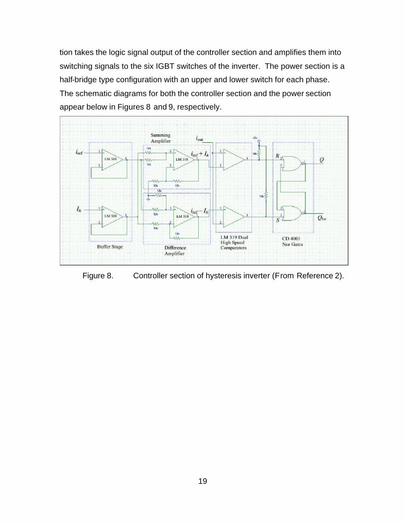
19
tion takes the logic signal output of the controller section and amplifies them into
switching signals to the six IGBT switches of the inverter. The power section is a
half-bridge type configuration with an upper and lower switch for each phase.
The schematic diagrams for both the controller section and the power section
appear below in Figures 8 and 9, respectively.
Figure 8. Controller section of hysteresis inverter (From Reference 2).

20
Figure 9. Power section of hysteresis inverter (From Reference 2).
The hysteresis inverter viewed as a subsystem is represented in the block
diagram in Figure 10 below.
controllersection
SemikronSKHI 22BGate drivers
Power section
3-phaseload
iHabciH*
abc
+-
logic signals gating signals
Figure 10. Block diagram of hysteresis inverter (After Reference 2).
The block diagram in Figure 10 shows that the hysteresis inverter provides
the unique advantage of a closed-loop system for the control of the load current.
The closed-loop control will provide the key to the successful operation of the

21
entire system when paralleled with the bulk inverter described in the following
sections.
C. BULK INVERTER
The bulk inverter produces a three-phase, six-step output to supply the
majority of the current at the fundamental frequency in the overall system. It is
an open-loop Voltage Source Inverter (VSI). The bulk inverter also provides the
reference current signal for the hysteresis inverter controller.
Constructed from discrete components, the bulk inverter consists of sev-
eral elements that work in concert to create a three-phase output. The system
block diagram for the bulk inverter controller is depicted in Figure 11. The three
voltage reference signals that appear in the figure are used to determine cross-
over points by the comparator circuit.
60-Hzsignal generator -120O
-120O
VAref
VBref
comparatorcircuit forbulk inverter
gate driver(x6)
Logic signals
switch gate control signals to IGBTs
A
B
C
12
3456
high frequency acpower supply for gate drivers
to hysteresis invertercontroller
VCref
Figure 11. System block diagram of bulk inverter controller.
The timing of the switches in the bulk inverter and the reference current
waveform for the hysteresis inverter both come from the same 60-Hz oscillator.
The schematic diagram in Figure 12 shows the simple design used to realize the
oscillator.
This circuit produces a steady sinusoidal signal at a frequency of 60 Hz
with an amplitude of 10 V peak. The output of the oscillator serves as phase A of

22
the inverters. To create the other two phases of the inverters, the phase A signal
is shifted by 120° sequentially to produce phases B and C. The phase-shifter
circuit used appears in Figure 13.
_
+
D1
D2 3 kΩ
1 kΩ
1 kΩ
3 kΩ
25 kΩ.1 µF
25 kΩ.1 µF
20.3 kΩ
10 kΩ
- 15V
+ 15V
VAref
Figure 12. 60-Hz signal generator circuit (After Reference 6).
VAref
from 60-Hz signal generator
_
+
100 kΩ
100 kΩ
46 kΩ
.1 µF
_
+
100 kΩ
100 kΩ
46 kΩ
.1 µF
VBref VCref
Figure 13. Phase-shifter circuit (After Reference 7).

23
In order to control the switches for each of the three phases of the bulk in-
verter, the sinusoidal reference signals pass through a network of comparator
circuits. Based on the LM311 comparator, these circuits take the reference sig-
nal input and produce square-wave pulse signals to the upper and lower
switches of the bulk inverter. This network is shown in Figure 14. The reference
signal labeled as Vref represents any of the three phase reference signals (VAref,
VBref, or VCref) depicted in Figure 13. The top comparator circuit will send a gate
signal of +15 V to the upper switch when the reference signal exceeds a thresh-
old of 2.5 V. Therefore, the comparator will generate a positive voltage signal for
most of the positive half cycle of that particular phase. The other comparator on
the bottom will correspondingly send a positive logic signal to the lower switch
when the reference voltage falls below –2.5 V. A small hysteresis current
through the positive feedback loop ensures that the output does not oscillate at
the transitions. The threshold for the logic signal switching was set to 2.5 V to
guarantee that an upper and lower switch in the same phase-leg are not acti-
vated simultaneously.
+_
+_
+15V
10 kΩ
2 kΩ
100 kΩ
100 kΩ
LM311
LM311
+15V
+15V
-15V
2 kΩ
Vref
1 kΩ
1 kΩ 510 Ω
510 Ω
Logic signal toS1, S3, S5
Logic signal toS2, S4, S6
Figure 14. Comparator circuit to generate logic signals to switches.

24
The controller for the bulk inverter also serves as the reference signal
source for the hysteresis inverter. The same signal that generates the logic sig-
nals to phase A of the bulk inverter drives the timing of the hysteresis inverter.
After it leaves the bulk inverter controller, the current reference signal passes
through a basic amplifier that sets the desired magnitude of the output load cur-
rent. The signal then passes through a phase-shifter that can set the overall
phase shift between the reference signal and the bulk inverter phase voltage.
This signal then goes into the hysteresis inverter as the phase A current refer-
ence signal. A pair of phase-shifters identical to those depicted in Figure 13
generates the reference current signals for phases B and C of the hysteresis in-
verter. Figure 15 shows the schematic diagram for this hysteresis signal refer-
ence circuit.
Figure 15. Hysteresis signal reference circuit.
In the configuration above, the first-stage amplifier has a variable resistor
in the feedback loop labeled as Rf. The desired magnitude of the reference cur-
rent signal to the hysteresis inverter can be set by adjusting the value of Rf. The
value of the input resistor is fixed at 20 kΩ and the amplitude of the reference
signal input is 10 V. The magnitude of the current reference signal, Iref, complies
with the following equation:

25
= =3
10.
20 10 2000f f
refR R
Ix
(3-2)
The actual reference current signal will follow a 1:1 relationship with the voltage
signal Iref in Equation 3-2. In the experimental configuration studied, the value of
Rf is 10 kΩ to reduce the magnitude of the reference signal Iref to 5 V. This
commands the hysteresis inverter controller to maintain the load current ampli-
tude at 5 A.
The phase shift of the reference current relative to the bulk inverter phase
voltage will depend on the value of Ri in the variable phase shifter depicted in
Figure 15. For this application, the value of Ri was varied using a 0–100 kΩ po-
tentiometer. Following the same principles as the phase shifter circuits in Figure
13, the amount of phase shift depends on the RC time constant of the circuit and
the input frequency, f, as illustrated by [7]:
φ π−= 12tan (2 ).i ifRC (3-3)
With the capacitance Ci held constant and f set at 60 Hz, the variable resistance
Ri can be adjusted with the potentiometer to obtain the desired phase shift.
The circuits depicted above were built from discrete components on com-
mon wire-wrap breadboard. A printed circuit board with copper on both sides
surrounded the circuit and supported a common ground plane, a positive supply
input, a negative supply input, and connections for the system outputs. Tables
contained in Appendix A list the specific pin connections of the components.
From the comparator circuit (Figure 14), the logic output signal passes into
the gate driver circuit (Figure 17). This circuit converts a logic signal into an ap-
propriate level to properly gate an IGBT in the bulk inverter power section; a To-
shiba TLP250 photocoupler is the main component. The gate driver circuit is also
necessary for providing electrical isolation. The control circuitry must be isolated
from the high voltage and current associated with actual inverter switches. Fur-
ther, isolation is necessary between individual switches. Reference 8 provides a
more detailed description of the gate driver circuit.

26
An amplified square wave input provides the basic power to the TLP250
via a high-frequency transformer (Magnetek GDE25-2) and a full-bridge rectifier
(using four 1N4148 fast-recovery diodes). A common amplifier supplied the
power for all six gate driver circuits. A function generator set at 20 kHz was used
for the input to the amplifier. A 1-µF capacitor filters out high frequency noise at
the output of the circuit to ensure that only the low frequency switching signal
gets to the transistors. The circuit diagrams for the signal amplifier and the gate
driver circuit are depicted below in Figures 16 and 17, respectively.
+_LM12
-15V
+15V
1 kΩ
3.3 kΩ
1.1 kΩ
1 µF2200 µF
2200 µF
1.5 nF
UF1003
UF1003
VINPUT
VOUTPUT
+
_
+
_
Figure 16. Amplifier circuit for square wave signal.
high freqtransformer1:1low couplingcapacitanceMagnetekGDE25-2
±15V20 kHzsquare waveac input(capable of ±10A)- from amplifier
Full-wavebridge rectifier
+15V dc
-15V dc
TLP250photocoupler
8
5
2 3
Logic signalInput
- +
360 Ω
65.1 Ω
1 µF1 µF
1 µF
Output to IGBT gate
+
-
-
+
1 µF
1 µF
1 µF
Figure 17. Gate Driver Circuit (After Reference 8).

27
The six identical gate driver circuits supplied the triggering signals to the
six bulk inverter IGBTs to produce an alternating current. The transistor switches
utilized were the Toshiba MG50Q2YS9 which combined the upper and lower
switches and diodes for each phase in the same package. Each switch is rated
for = 1200 VCEV and = 50 A.CI The total switching delay time for the IGBT is
calculated below.
( ) ,on d on rt t t= + (3-4)
and
( ) ,off d off ft t t= + (3-5)
where = µ = µ = µ( ) ( ) 0.8 s, 0.6 s, 1.8 s,d on r d offt t t and = µ 1.0 sft [9].
From the data presented above, the total time required to turn the IGBT
on is 1.4 µs and the total time to turn it off is 2.8 µs. Therefore, the total switch-
ing delay for each cycle is 4.2 µs. The maximum allowable switching frequency
of the transistor can then be computed as:
µmax
1 1 = = = 238.1 kHz.
+ 4.2 son off
ft t
(3-6)
The actual delay of the IGBT used is insignificant when coupled with the
gate driver circuit used in this inverter. The measured delays are 100 µs and 90
µs for turn-on and turn-off, respectively. Therefore, the total delay of 190 µs far
exceeds the IGBT switching time of 4.2 µs. Given the above delay, the maxi-
mum operation frequency drops to 5.2 kHz. Since each switch in the power sec-
tion of the bulk inverter will only turn on and off at a rate of 60 Hz, this frequency
limitation is not an issue.
D. SYSTEM CONFIGURATION
As configured in Figure 18, the bulk and hysteresis inverters are combined
via inductors prior to the load. Ideally, the bulk inverter will provide all of the re-
quired current at the fundamental frequency of 60 Hz while the hysteresis in-
verter will add the current components necessary to cancel harmonics in order to
shape the waveform to match the reference signal. The closed-loop system pro-

28
vided by the hysteresis inverter will continuously adjust the load current within the
tolerance band to ensure that it stays at the desired level.
Figure 18. Power section topology of hybrid inverter. In Figure 18, the two inverters are connected in parallel to drive a common
three-phase wye-connected resistive load. Although this diagram depicts a
purely resistive common load, the hybrid inverter can drive a load with a lagging
power factor as well. In the experimental testing of the system, the value of RL is
1.05 Ω and the inductances L are 9.1 mH.
The detailed designs of the components that comprise the hybrid inverter
were presented in this chapter. The design of the hysteresis inverter element
was described as well as the fabrication of the six-step bulk inverter control cir-
cuits and power section. The following chapter will expand on the theoretical
predictions for the system performance and simulate the operation of the newly
constructed bulk inverter.

29
IV. THEORETICAL RESULTS
The hybrid inverter system combines two predictable elements to form a
unique composite topology to produce ac power. This chapter presents the the-
ory behind their operation.
A. OVERALL PERFORMANCE
The requisite load of the hybrid inverter consists of an inductive element
and a resistive element. In the configuration studied, the output of each inverter
is connected to a separate inductor that feeds current into a parallel-connected
load. A model of the topology used in this experiment is depicted in Figure 19
below. The figure depicts the combined phase A of the parallel-connected in-
verters. The topology for phases B and C are identical.
S1
S2
D1
D2
S1
S2
D1
D2
Vdc
-Vdc
Bulk inverter(phase A)
Hysteresis inverter(phase A)n (neutral point)
RL
L L
IB IH
IL
-Vdc
Vdc
a
b c
Figure 19. Topology of single phase of hybrid inverter.
As discussed in the previous chapter, the load current consists of the sum
of the output currents of the bulk and hysteresis inverter sections. The induct-

30
ances on the output of each inverter are of equal value and they are connected
to a three-phase, balanced resistive load. The neutral point is floating in this con-
figuration. In order to evaluate the resultant load current, iL, the current compo-
nents produced by each inverter section are computed individually. By the prin-
ciple of superposition, the hysteresis inverter is replaced with an open circuit and
the load current produced by the bulk inverter is computed. Similarly, the bulk
inverter is replaced by an open circuit while the hysteresis inverter current is
quantified. The total load current is found by simply adding the two separate cur-
rent components coming into the node at point “a”.
B. HYSTERESIS INVERTER CURRENT
The current produced by the hysteresis inverter follows the model devel-
oped in Reference 2. Utilizing two-level switching, the hysteresis inverter applies
either +Vdc or –Vdc across the load. Therefore, two simple equations describe the
current across the load for each case. For the case where the positive dc voltage
is applied, the load current complies with [2]
− −− −
= + −
0 0( ) ( )
0( ) ( ) 1 .R Rt t t t
dcL LL L
Vi t e i t e
R (4-1)
When the hysteresis inverter applies the negative dc voltage to the load,
the negative sign appears in front of the Vdc term in Equation 4-1 and the current
is described by [2]
− −− − −
= + −
0 0( ) ( )
0( ) ( ) 1 .R Rt t t t
dcL LL L
Vi t e i t e
R (4-2)
The above set of equations show that there must be an appropriate
amount of inductance L in the circuit in order to prevent the load current from
changing instantaneously. It also indicates that larger time constants will slow
the rate of change of the current. This translates to a slower rate of switching for
the controller given a fixed hysteresis band and bus voltage. Since L is generally
fixed, the load range for optimal operation of the converter will be restricted. The
predicted switching frequency can be computed from the system parameters us-
ing Equation 2-5 as discussed earlier in the thesis.

31
C. BULK INVERTER CURRENT
Contrary to the hysteresis inverter, the applied voltage of the bulk inverter
follows a prescribed pattern with six discrete steps in each cycle. Each phase
voltage waveform is separated by a phase shift of 120° from the other two
phases. The voltages applied to the load depend only on the dc bus voltage and
there is no feedback input from the inverter output.
Figure 20 depicts the voltage steps of phase A for one period of a refer-
ence 60-Hz sine wave. The bulk inverter produces a quantized representation of
the sinusoidal reference signal. On the y-axis labels of Figure 20, the quantity
∆Vdc is defined by the total voltage across the dc bus from +Vdc to –Vdc. If the
positive and negative bus voltages are equal in magnitude, the then the value of
∆Vdc would be equal to 2Vdc. Since there are only four possible voltage levels,
the bulk inverter produces a relatively rough approximation of the desired sinu-
soidal waveform and will generate considerable harmonic content above the fun-
damental frequency.
voltage applied to load
reference signal (60 Hz)
ωt60O 120O
180O
240O 300O
360O
23 dcV∆
13 dcV∆
Figure 20. Phase A applied voltage for bulk inverter (From Reference 3).
To produce the various steps throughout the cycle on the phase voltage
waveform, the bulk inverter opens and closes each of the six switches in the
power section in a specified pattern. Each switch is closed for 180O out of the
360O cycle and open for the remainder. The prescribed switching algorithm for

32
the six-step bulk inverter is listed in Table 1 below. Refer to the bulk inverter to-
pology diagram in Figure 18 for the position of the inverter switches 1 -6.
Switch state Interval
(degrees) Switch 1 Switch 2 Switch 3 Switch 4 Switch 5 Switch 6
0-60 closed open open closed closed open
60-120 closed open open closed open closed
120-180 closed open closed open open closed
180-240 open closed closed open open closed
240-300 open closed closed open closed open
300-360 open closed open closed closed open
Table 1. Switching algorithm for six-step bulk inverter.
The rate of change of the current varies as the voltage applied across the
load steps through each discrete level. With a purely resistive load, the current
waveform matches the voltage waveform. However, the addition of inductive
elements in the load makes the current waveform lag behind the voltage wave-
form in the time domain. For phase A, the current across the load complies with
the following relation:
− −− −
= + −
0 0( ) ( )
0
( )( ) ( ) 1 .
R Rt t t tanL L
La La
V ti t e i t e
R (4-3)
In Equation 4-3, the initial conditions, t0 and iLa(t0), are reset to the instantaneous
value when a switching event occurs during the cycle and the phase voltage,
Van(t), steps to the next value. For example, if Van(t) doubles in magnitude from
? ∆Vdc to ? ∆Vdc at time t = 2.8 ms, then the value of t0 would become 2.8 ms
and the new value of iLa(t0) would be the magnitude of the phase A load current
at that time. The current follows the simple exponential relation in Equation 4-3

33
with these initial conditions and a constant applied voltage until the voltage steps
to the next value 2.8 ms later. With a 60-Hz fundamental frequency, a switching
event occurs every 2.8 ms, which corresponds to a change of 60 ,tω = ° a product
of frequency and time.
Similar to the relationship described for phase A, the load currents for the
bulk inverter for phase B and phase C are quantified by
− −− −
= + −
0 0( ) ( )
0
( )( ) ( ) 1 .
R Rt t t tbnL L
Lb Lb
V ti t e i t e
R (4-4)
− −− −
= + −
0 0( ) ( )
0
( )( ) ( ) 1 .
R Rt t t tcnL L
Lc Lc
V ti t e i t e
R (4-5)
The above equations form the basis of the simulation created to model the load
current generated by the bulk inverter. A MATLAB script file was used to plot the
expected load current and voltage for the bulk inverter with an applied dc bus of
39 V and a load of 1.05 Ω in series with 9.1 mH for each phase. Appendix B
contains the MATLAB code for the simulation. The phase current and voltage for
the bulk inverter appear in Figure 21.

34
Figure 21. Results of simulation of bulk inverter, phase A.
In the simulation of the bulk inverter, the phase A voltage followed the six-
step pattern described earlier. With a total applied dc bus voltage of 39 V, the
phase A voltage stepped through the discrete levels of 12 V, 24 V, –12 V, and –
24 V to approximate a sinusoidal reference signal. The simulation accounted for
a voltage drop of 2 V across each switch as specified on the data sheet for the
IGBT used [9].
The phase A load current in Figure 21 is scaled by a factor of 4 to amplify
the waveform with respect to the phase voltage. From Figure 21, the phase A
current lags behind the phase A voltage by 3.5 ms. At a frequency of 60 Hz, the
time delay of 3.5 ms corresponds to a phase shift of –75°. The large phase shift
reflects the heavily inductive load in the simulated circuit. The angle of the phase
shift depends on the characteristics of the load and is computed by:

35
1cos ,n
n
RZ
θ − =
(4-6)
where θn is the phase shift at harmonic number n and Zn is the total impedance
at the nth harmonic.
The magnitude of Zn can be calculated from the resistance and reactance
components of the load as follows:
2 2( ) ,nZ R jn L1 = + ω (4-7)
where R is the load resistance, ω1 represents the fundamental frequency, and L
is the load inductance. Consisting of a 9.1 mH inductor coupled with a 1.05 Ω
resistor, the load in the circuit has an angle of 73° at the fundamental frequency
of 60 Hz ( )1n = . The higher harmonic components will have different total im-
pedances and, therefore, they will be shifted in phase to a greater extent. The
actual current waveform for the bulk inverter will lag behind the voltage by a
phase shift greater than 73° due to its significant harmonic content. As a result,
the simulation produced a larger phase shift of 75°.
Figure 22 shows a detailed view of the three phase currents in the time
domain for the bulk inverter operating independently.

36
0.4 0.405 0.41 0.415 0.42 0.425-8
-6
-4
-2
0
2
4
6
8Phase Currents of Bulk Inverter
Time (sec)
Cur
rent
(A)
Phase APhase BPhase C
Figure 22. Phase A, B, and C currents of the bulk inverter
( )39 VdcV∆ = .
The detailed view of the current waveforms reveals that the phase cur-
rents of the bulk inverter change in slope at six distinct points throughout the cy-
cle. These points correspond to the switching events that occur every 2.8 ms, or
60°, to step the phase voltage to the a new level. Although the waveforms
roughly follow the shape of the sinusoidal reference signal, the sharp corners at
each transition point translate into higher frequency harmonics in the frequency
spectrum of the waveform. The theoretical harmonic content of the current
waveform can be derived from the magnitude of the harmonics present in the
phase voltage waveform. The Fourier series expression for the six-step bulk in-
verter phase A voltage is [10]

37
( ) ( ) ( ) ( )
1
1
1 12 2cos cos (6 1) cos (6 1) .
6 1 6 1
k k
an dc dck
v V V k kk k
θ θ θπ π
+∞
=
− − = + − + + − +
∑ (4-8)
The magnitude of the Fourier coefficients at each integer non-zero har-
monic frequency for the bulk inverter current will follow the relation:
,nn
n
BI =
Ζ (4-9)
where In is the magnitude of nth harmonic of phase current waveform, Bn is the
magnitude of nth harmonic of phase voltage, and Zn is the load impedance at nth
harmonic frequency.
Since nω1L > R for all harmonics, the impedance Zn will be the dominant
term in Equation 4-9. This will considerably decrease the magnitude of the
higher harmonics of the load current waveform. Using the equations above, the
frequency spectrum was predicted for the six-step bulk inverter operating with a
dc bus voltage of 39 V. The results are depicted in Figure 23.

38
Figure 23. Theoretical harmonic content of bulk inverter phase current.
The number of each non-zero harmonic is depicted above each data point
on Figure 23 where Zn = 1.05 + jnω10.0091 Ω. The magnitude of each harmonic
in the load current was computed in accordance with Equations 4-8 and 4-9. Us-
ing Equation 2-3, the theoretical THD of the six-step bulk inverter current was
calculated to be 4.83% including the first 31 harmonics. Similar analysis revealed
that the corresponding phase voltage waveform depicted in Figure 21 had a THD
of 30.48%. This difference illustrates the significant effect that the load induc-
tance has on the THD of the load current waveform.
This chapter presented the principles that govern the current produced by
the hysteresis and bulk inverters. The expected current and voltage waveforms
were created for the six-step bulk inverter using a MATLAB simulation. By apply-

39
ing the Fourier series expansion, the magnitude of the non-zero harmonics for
the bulk inverter current waveform was computed. The theoretical THD of the
phase current was 4.83% for the design load of 9.1 mH in series with a resis-
tance of 1.05 Ω.
With the addition of the hysteresis inverter in parallel with the bulk inverter,
the hybrid inverter system attempts to reduce this harmonic content. The next
chapter will detail the results of the hardware implementation of the hybrid in-
verter system and measure its performance against the design goals.

40
THIS PAGE INTENTIONALLY LEFT BLANK

41
V. EXPERIMENTAL RESULTS
Following the completion of the hardware fabrication process, the hybrid
inverter system was tested in several stages to assess its performance and de-
termine the optimal operating mode. Each individual subsystem was tested be-
fore the system was configured to operate as a unit.
A. PRELIMINARY TESTING OF BULK INVERTER
The predicted performance characteristics of the six-step bulk inverter ap-
pear in the simulation results of the previous chapter. The simulation results
served as a benchmark against which to measure the actual current waveform
produced by the bulk inverter.
In the preliminary testing, the bulk inverter was connected to a floating-
neutral, balanced, wye-connected load. Each phase of the load consisted of 9.1
mH inductance in series with 1.05 Ω of resistance. The resultant peak magni-
tude of the line-current was 5 A. The inductors used were the InverPower Con-
trols reactor rated for 10 A continuous current and a total inductance of 42.5 mH
and taps at 5% intervals. The load inductance of 9.1 mH was measured from the
30% tap of the inductor. The Hewlett-Packard 6002A DC Power Supply served
as the dc-link voltage source with an overall range of 0–50 V for ∆Vdc. With ∆Vdc
= 39 V, the bulk inverter produced the following current and voltage waveforms
found in Figure 24 for each of the three phases.

42
Figure 24. Bulk inverter phase current and voltage.
The bulk inverter voltage waveform in Figure 24 generally conformed to
the six-step pattern of the simulation results depicted in Figure 21 in the previous
chapter. Each change in the voltage level corresponded to a switching event,
and voltage stepped through six discrete levels in the course of one cycle. The
applied total voltage across the dc bus was 39 V for this test, as in the MATLAB
simulation.
As the voltage steps through the sequence of levels, the phase current
changes based on the RL load time constant and the applied voltage. The cur-
rent changes at the fastest rate when the phase voltage reaches its minimum
magnitude o f 24 V as seen in Figure 24. Since the load is inductive, the current
lags the voltage by 85°.
The experimental phase shift was greater than the phase shift of 75° ob-
served in the MATLAB simulation. The difference was most likely caused by a
discrepancy in the measured inductance and the actual inductance of the load L
at 60 Hz. Since the actual inductance of inductors used in the experiment vary
with frequency [2], the load may have actually had more inductance at 60 Hz
phase current (2.0 A/div)
phase voltage (10 V/div)

43
than the value measured by the instrument. This would cause the phase shift to
be higher.
Although they both follow the same overall pattern, the results from the
simulation did predict a higher peak value of the current (6.0 A) than the current
produced by the actual hardware (5.4 A). The 10% error in the experimental cur-
rent magnitude compared to the simulation results was most likely caused by the
errors in the inductor values mentioned above, underestimated voltage drops in
the IGBT switches and diodes, or switching delay times. Other than this differ-
ence, the actual results corresponded with the current waveforms produced in
the simulation.
The six-step bulk inverter performed as predicted by the theoretical
analysis and it proved suitable for coupling with the hysteresis inverter to form
the hybrid inverter system.
B. THREE-PHASE TESTING OF HYSTERESIS INVERTER
The hysteresis inverter had been built and tested during a previous re-
search effort with good results as an independent unit [2]. The original testing
provided baseline results. The baseline results used a dc bus voltage of 20 V and
a load of 9.1 mH in series with a 1-Ω resistance. A peak load current of 2 A was
produced with a hysteresis band of 0.06 A. However, in order to use this inverter
with the bulk inverter in the hybrid system, the three-phase reference signal must
come from the bulk inverter and not the original hysteresis inverter signal genera-
tor. Therefore, independent testing of the hysteresis inverter was repeated using
the hysteresis signal reference circuit (Figure 15) at the baseline and then at the
desired 5-A system peak load current. The three-phase output current is de-
picted in Figure 25.

44
Figure 25. Phases A (top), B (middle), and C (bottom) of hysteresis
inverter operating independently with Ih = 0.1 A and ∆Vdc = 39 V. (5.0 A/div)
The results depicted in Figure 25 confirm that the hysteresis inverter
worked as designed with the new hysteresis signal reference circuit created for
the hybrid inverter system. The testing done in the previous research effort was
revalidated as the current waveform matched the sinusoidal reference signal at 5
A peak magnitude.
C. SINGLE-PHASE PARALLEL TESTING
Prior to commencing testing and optimization of the complete three-phase
hybrid inverter system, a preliminary trial of one individual phase was conducted
to verify that the bulk and hysteresis inverters would work in conjunction with one
another. The results closely resembled the waveforms produced in Reference 2.
The parallel combination of one phase of the bulk inverter and one phase of the
hysteresis inverter produced a sinusoidal output current to a load of 9.1 mH in

45
series with a 1.05-Ω resistance. Tests of the other two phases yielded similar
results.
The single-phase experimental trials revalidated the previous results and
confirmed that the parallel combination of the bulk and hysteresis inverter ele-
ments would work together as designed.
D. THREE-PHASE PARALLEL TESTING
After seeing acceptable results during single-phase testing, the hybrid in-
verter system was reconfigured for three-phase operation. The objective of the
testing was to provide answers to the following questions:
• Can the hybrid inverter system produce a high-fidelity sinusoid from
the reference?
• How can the hybrid inverter system be optimized to draw all of the
fundamental load current from the bulk inverter and minimize the
current produced by the hysteresis inverter?
Variables in the hybrid inverter system that could be controlled were the
width of the hysteresis band, the phase shift between the bulk and hysteresis
inverters, the input dc bus voltage level, the composition of the load, and the size
of the load combining reactances. The experimental process aimed to adjust
each of these independent parameters to find the optimal combination to produce
the waveform that most closely matched the sinusoidal reference signal. In addi-
tion to obtaining the highest quality load current waveform, the secondary objec-
tive was to minimize the magnitude of the current produced by the hysteresis
inverter at the fundamental frequency and to make the bulk inverter produce vir-
tually all of the useful power. Minimizing the current share of the hysteresis in-
verter would enable the smallest possible hysteresis inverter to be used and it
would make the overall hybrid inverter system more compact.
The hybrid inverter was configured as depicted in Figure 18 with each in-
verter phase output passing through a 9.1 -mH inductor and then into the com-
mon phase load of a 1.05-Ω resistor. The neutral point was floating in the middle
of the balanced wye-connected load. After several iterative adjustments to the

46
dc bus voltage, the phase shift between inverters, and the width of the hysteresis
band, the optimal operating point was found. The phase currents from phases A,
B, and C at the optimal operating point are shown from top to bottom respectively
in Figure 26.
Figure 26. Phases A, B, and C in parallel operation (5.0 A/div) .
In order to produce these results, the phase shift between the bulk and
hysteresis inverters was 55°, the dc bus voltage ∆Vdc was set to 30.8 V, and the
width of the hysteresis band Ih was approximately 0.1 A. Figure 27 shows a
closer view of the three phase currents on the same x-axis.

47
Figure 27. Detailed view of phase A, B, and C currents (2.5 A/div).
The above figures affirm that the output current of the hysteresis inverter
coupled in parallel with the bulk inverter closely resembles a sinusoid.
The objective of the hybrid inverter was to produce a high-fidelity load cur-
rent waveform and reduce the THD of the bulk inverter load current. The output
current waveforms of both the hybrid inverter and the bulk inverter operating in-
dependently were analyzed using the Hewlett Packard 3561A Dynamic Signal
Analyzer. The frequency spectrum of a representative phase of the load current
produced by the bulk inverter appears below in Figure 28.

48
Figure 28. Frequency spectrum of bulk inverter (10 dB/div, 0-2000 Hz).
The observed frequency spectrum of the bulk inverter closely resembles
the predicted harmonic content shown in Figure 23 in the previous chapter.
Including the first 20 harmonics, the current THD was calculated to be 5.5% by
the spectrum analyzer. This experimental THD was slightly higher than the theo-
retical THD of 4.83%. The actual THD was most likely higher because the odd
triplet harmonics are suppressed but not completely cancelled as in the theoreti-
cal calculations.
Although the bulk inverter did produce a load current with relatively low
harmonic content, the addition of the hysteresis inverter further reduced the
overall THD. The frequency spectrum of the hybrid inverter phase load current is
shown in Figure 29.

49
Figure 29. Frequency spectrum of hybrid inverter (10 dBV/div, 0-2000 Hz).
Figure 29 shows that the lower-order harmonics were at least 35 dB
smaller than the fundamental for the hybrid inverter. The fifth and seventh har-
monics made the largest contribution to the THD in the bulk inverter, but they
were attenuated by at least 10 dB in the hybrid frequency spectrum. The per-
centage THD was 3.2% for the hybrid inverter spectrum up to the 20th harmonic.
Since the hysteresis inverter switched at a variable frequency, the harmonics
produced by the switching operations were spread across the spectrum and did
not appear as a dominant harmonic at a fixed frequency.
Based on the frequency spectrum analysis, the addition of the hysteresis
inverter improved the overall THD of the load current waveform of the bulk in-
verter from 5.5% to 3.2%. These results affirmed that the hybrid inverter could
produce a high-fidelity output load current.

50
Although the hybrid inverter met its overall objective to produce a clean si-
nusoidal output current, it fell short of the design goal of limiting the fundamental
current to the bulk inverter. While phase B of the hysteresis inverter produced
only canceling harmonics, phases A and C provided a share of the fundamental
load current.
In the phase A load current depicted in Figure 30, the bulk inverter pro-
vides approximately 3.5 A of the 5.0 A total current across the load while the hys-
teresis inverter makes up the difference with the other 1.5 A. Ideally, the bulk
inverter would produce about 5.0 A at the fundamental frequency while the hys-
teresis inverter only injected current to cancel harmonics higher than 60 Hz in the
bulk current waveform.
Figure 30. Hybrid Phase A – Bulk and Hysteresis phase currents
(2A/div) .
Figure 31 shows the results for phase B. The currents for each inverter
element in phase B approach the ideal objective described above. It contributes
Bulk inverter
Hysteresis inverter

51
almost no current at the fundamental frequency of 60 Hz. The bulk inverter in
phase B produced about 4.8 A peak at the fundamental frequency, while the hys-
teresis inverter current stayed below 1 A for the entire cycle. As expected, the
hysteresis inverter switched at a frequency much higher than the fundamental in
order to cancel the harmonics and to maintain the sinusoidal shape of the load
current waveform.
Figure 31. Hybrid Phase B – Bulk and Hysteresis phase currents (2 A/div).
The balance between the bulk and hysteresis inverter currents for phase
C appears in Figure 32. As in phase A, phase C of the hysteresis inverter con-
tributed a portion of the load current at the fundamental frequency. The results
are slightly more optimal than those of phase A. Thus, the hysteresis inverter
provides the right amount of current to augment the 4.0-A peak produced by the
bulk inverter.
Bulk inverter
Hysteresis inverter

52
Figure 32. Hybrid Phase C – Bulk and Hysteresis phase currents (2 A/div).
E. ZERO-SEQUENCE CURRENT
In a balanced, three-phase system, the sum of the three phase currents
will add to zero for any time in the cycle due to the 120° phase separation be-
tween each of the current vectors. The currents theoretically will comply with the
following relation:
+ + =( ) ( ) ( ) 0.a b ci t i t i t (5-1)
The instantaneous sum of all three phase currents is called the zero-sequence
current. The zero-sequence current should stay at zero at all times during the
cycle.
However, the experimental testing of the three-phase hybrid inverter re-
vealed a small but persistent zero-sequence current present in the circuit. Al-
though it did not disrupt the three line current waveforms, the zero-sequence cur-
Bulk inverter
Hysteresis inverter

53
rent appeared as a low frequency oscillation on the input current waveforms from
the hysteresis inverter and the bulk inverter. Connecting the two inverters in par-
allel created a path for the zero-sequence current to flow. Figure 33 depicts the
effect of the zero-sequence current and the ripple caused by it on the output cur-
rents of the bulk and hysteresis inverters.
Figure 33. Effect of zero-sequence current on hybrid circuit (2 A/div)
The large amplitude waveform represents the bulk inverter current and
the smaller amplitude waveform near the x-axis traces the hysteresis inverter
current. The zero-sequence current causes the ripple in the two waveforms at
low frequency over several cycles. This low frequency ripple caused the jitter in
the waveforms when observed on the oscilloscope. Figure 33 shows the dy-
namic interaction between the inverters as the hysteresis inverter current in-
creased when the bulk inverter decreased.
The zero-sequence could be caused by a slight imbalance in the actual
phase shift between current vectors, a small difference in the load impedances,
Bulk inverter
Hysteresis inverter

54
or the dynamic interaction between the inductors connected to the hysteresis and
bulk inverters on each phase.
In an attempt to eradicate the zero-sequence current, the neutral point
was temporarily clamped to the midpoint of the dc bus. This modification had no
effect on the oscillations caused by the zero-sequence current, so the neutral
point was returned to its floating state. An unbalanced load was the suspected
cause of the zero-sequence current. However, more precise matching of the
load elements failed to correct the problem.
One effective way to eliminate the zero-sequence current as well as the
imbalance between phase currents would be to implement a new control strategy
in the quadrature-direct-zero (qd0) reference frame. Common in motor drive
control, the qd0 strategy would provide control over the composite three-phase
system by transforming the three phase currents into two equivalent orthogonal
quantities and a zero-sequence term [10].
F. SUMMARY OF RESULTS
In the experimental testing phase of this research effort, the hybrid inverter
system was evaluated against expected performance parameters to validate the
design. After verification of each subsystem independently, the hysteresis in-
verter was coupled in parallel with the bulk inverter and tested in its design con-
figuration to verify that it met the prescribed objectives.
The testing revealed that the hysteresis/bulk hybrid inverter produced a
high-fidelity load current waveform with a peak amplitude of 5 A. The addition of
the hysteresis inverter to the bulk inverter significantly reduced the THD of the
current waveform. Therefore, the first objective of the testing was met as the
hybrid inverter produced a high-fidelity sinusoid from the reference.
The second objective was to optimize the system such that all of the fun-
damental current was produced by the bulk inverter. Thus, the power output of
the hysteresis inverter would be minimized. This load-sharing strategy would
capitalize on the strengths of each inverter element and allow for smallest possi-
ble hysteresis inverter. Experimental results revealed that the optimal operating

55
point was achieved at a dc bus voltage of 30.8 V, a phase shift of 55° (between
the bulk and hysteresis inverters), and a hysteresis band of 0.1 A. However, a
larger than desired portion of the fundamental load current was contributed by
the hysteresis inverter despite attempts to draw all of the fundamental load cur-
rent from the bulk inverter. It became clear that a further refinement of the con-
trol strategy would be necessary to alleviate an imbalance caused by zero-
sequence current.

56
THIS PAGE INTENTIONALLY LEFT BLANK

57
VI. CONCLUSION
With the experimental testing complete, the results can be measured
against the original research questions. The results of this thesis effort also bring
up new initiatives and further questions for future exploration.
A. REVIEW OF RESEARCH QUESTIONS AND GOALS
This research effort sought to explore the concept of a hybrid inverter con-
sisting of a high fidelity hysteresis element coupled with a lower fidelity six-step
inverter. The goal was to verify that the two types of inverters would operate to-
gether in a parallel connected configuration with a balanced three-phase load.
The overall objective was to improve the fidelity of the bulk inverter output by
adding the hysteresis inverter. Experimental testing strived to determine the op-
timal operating point for the system where the hysteresis inverter delivered only
enough current to cancel the higher harmonics of the bulk inverter. The output
current waveforms for each phase were evaluated and compared to the desired
60-Hz sinusoidal reference current signal.
B. SUMMARY OF EXPERIMENTAL RESULTS
After the construction and preliminary testing of the six-step bulk inverter,
the hybrid inverter was configured by connecting the bulk inverter in parallel with
the existing hysteresis inverter across a three-phase balanced load. The hybrid
inverter produced a satisfactory three-phase output current at a level of 5.0 A
peak for each phase in experimental trials. The THD of the current waveform
improved from 5.5% for the bulk inverter alone to 3.2% for the hybrid combination
of the bulk and hysteresis inverters. The bulk inverter produced almost all of the
load current at the fundamental frequency in phase B, but the hysteresis inverter
contributed some of the fundamental load current in phases A and C. There was
also a small zero-sequence current present in the system which caused a low
frequency oscillation in the individual output waveforms of the hysteresis and
bulk inverters. The closed-loop feature of the hysteresis inverter enabled the
hybrid inverter to maintain a stable output current despite these disturbances.

58
During the experiment, the independent inputs of dc bus voltage, phase
shift between inverters, and hysteresis tolerance band were adjusted to deter-
mine the mode which produced the best results. Iterative trials revealed that a dc
bus voltage of 30.8 V, a phase shift of 55°, and a hysteresis band of 0.1 A de-
fines the optimal operating point for the system. The hybrid system produced a
high-fidelity current waveform at a frequency of 60 Hz and a magnitude of 5.0 A.
C. ANSWERS TO RESEARCH QUESTIONS BASED ON RESULTS
The experimental results obtained in this research effort validate the con-
cept of the hybrid inverter consisting of a hysteresis inverter and a six-step bulk
inverter connected in parallel. The addition of the hysteresis inverter offered an
overall improvement to the quality of the output of the bulk inverter and made a
higher quality current waveform. The hysteresis inverter also closes the current
control loop to respond to anomalies and disturbances in the system and ensure
that the load receives a constant, sinusoidal current at the desired magnitude.
The optimal operating point for the paralleled inverters was found after fine tuning
the input variables.
Although trials were conducted at a relatively low power level, the hybrid
system can be easily scaled to higher power levels with no modification. The
hybrid inverter developed in this thesis represents a viable alternative to existing
converter technology in providing a reliable current source for motor drives on
today’s naval vessels.
D. RECOMMENDATIONS FOR FURTHER DEVELOPMENT
This thesis represents only one phase in an ongoing effort to fully de-
velop the hybrid inverter for employment in motor drive systems. While the ques-
tions presented in this research effort were answered, additional questions were
created and more study is required to bring this concept into practical use.
As discussed in Chapter 5 previously, a zero sequence current caused a
low frequency oscillation in the circuit. Also, the output phase currents of the
hysteresis inverter did not all carry the same amount of current. This is not sur-
prising, since all three phases are controlled independently. A new control

59
scheme implementing the qd0 reference frame could potentially remedy these
issues and provide even more fidelity to the output waveform.
Since the hybrid inverter system was tested at a lower power level, further
testing needs to be performed at high power levels to verify its capability. The
actual bulk and hysteresis inverters were designed for much higher power in their
present configuration. They are only limited by the ratings of the IGBTs in their
respective power sections. It is estimated that the existing hybrid inverter system
could produce up to 100 kW at 480 V given a sufficient source and load.
The hysteresis inverter currently in use implements a two-state switching
algorithm to keep the current within the hysteresis band. It switches the phase
voltage between +Vdc and –Vdc as the current goes below and above the hys-
teresis band. Although this mode of operation produces satisfactory results, the
simulation performed in Reference 2 demonstrated that superior performance
could be achieved by the implementation of three-state switching. This improved
mode would switch the phase voltage between +Vdc and 0 when the reference
current is increasing and alternate the voltage applied between –Vdc and 0 when
the reference is decreasing. A modification or redesign of the existing hardware
would be necessary to add this feature to the hybrid inverter, but it could poten-
tially improve the fidelity of the output current.

60
THIS PAGE INTENTIONALLY LEFT BLANK

61
APPENDIX A. CIRCUIT WIRING DIAGRAMS
This appendix provides the specific layout and pin connections for the cir-
cuits described in Chapter 3.
Figure 34 displays the layout of the components on the main circuit board
for the bulk inverter controller. The 60 Hz signal generator, the phase-shifter cir-
cuits, and the comparator circuits are on this board. Tables 2–14 list the specific
pin connections for each 16-pin socket.
Figure 34. Component Layout Diagram for Bulk Inverter Controller.
Pin # Tie to component Tie to Pin # 1 VAref NC 16 2 A9 NC 15 3 B10 NC 14 4 +15V -15V 13 5 D2 D7 12 6 C10 D13 11 7 VBref
LF347
VCref 10 8 GND 10 kΩ B1 9
Table 2. Socket A wiring diagram.

62
Pin # Tie to component Tie to Pin # 1 A9 20 kΩ B15 16 2 A1 300 Ω B16 15 3 B9 24 kΩ B13 14 4 A1 1 kΩ B14 13 5 A3 24 kΩ B11 12 6 GND 1 kΩ B12 11 7 GND 0.1 µF A3 10 8 A3 0.1 µF B3 9
Table 3. Socket B wiring diagram.
Pin # Tie to component Tie to Pin # 1 -15V 3 kΩ C15 16 2 A1 1 kΩ C16 15 3 A1 1 kΩ C13 14 4 +15V 3 kΩ C12 13 5 A2 - diode 1 + C13 12 6 C16 - diode 2 + A2 11 7 A1 100 kΩ A6 10 8 A7 100 kΩ C10 9
Table 4. Socket C wiring diagram.
Pin # Tie to component Tie to Pin # 1 C7 43 kΩ D15 16 2 A5 3 kΩ D16 15 3 D2 + 0.1µF GND 14 4 A7 100 kΩ A11 13 5 A10 100 kΩ D13 12 6 D4 43 kΩ D10 11 7 A12 3 kΩ D11 10 8 D7 + 0.1 µF GND 9 Table 5. Socket D wiring diagram.

63
Pin # Tie to component Tie to Pin # 1 GND 0.1 µF +15V 16 2 GND 2 kΩ E5 15 3 GND E16 14 4 K16 Logic1 13 5 M1 NC 12 6 E9
LM311 comparator
NC 11 7 E13 510 Ω E16 10 8 GND 0.1 µF -15V 9
Table 6. Socket E wiring diagram.
Pin # Tie to component Tie to Pin # 1 GND 0.1 µF +15V 16 2 GND 2 kΩ E4 15 3 GND E16 14 4 M2 Logic2 13 5 K15 NC 12 6 E9
LM311 comparator
NC 11 7 E13 510 Ω E16 10 8 GND 0.1 µF -15V 9
Table 7. Socket F wiring diagram.
Pin # Tie to component Tie to Pin # 1 GND 0.1 µF +15V 16 2 GND 2 kΩ G5 15 3 GND G16 14 4 K12 Logic3 13 5 M1 NC 12 6 I9
LM311 comparator
NC 11 7 I13 510 Ω G16 10 8 GND 0.1 µF -15V 9
Table 8. Socket G wiring diagram.
Pin # Tie to component Tie to Pin # 1 GND 0.1 µF +15V 16 2 GND 2 kΩ H4 15 3 GND H16 14 4 M2 Logic4 13 5 K11 NC 12 6 H9
LM311 comparator
NC 11 7 H13 510 Ω H16 10 8 GND 0.1 µF -15V 9
Table 9. Socket H wiring diagram.

64
Pin # Tie to component Tie to Pin # 1 GND 0.1 µF +15V 16 2 GND 2 kΩ I5 15 3 GND I16 14 4 I16 Logic5 13 5 M1 NC 12 6 E9
LM311 comparator
NC 11 7 E13 510 Ω I16 10 8 GND 0.1 µF -15V 9
Table 10. Socket I wiring diagram.
Pin # Tie to component Tie to Pin # 1 GND 0.1 µF +15V 16 2 GND 2 kΩ J4 15 3 GND J16 14 4 M2 Logic6 13 5 I15 NC 12 6 J9
LM311 comparator
NC 11 7 J13 510 Ω J16 10 8 GND 0.1 µF -15V 9
Table 11. Socket J wiring diagram.
Pin # Tie to component Tie to Pin # 1 VAref (A1) 1 kΩ E4 16 2 K1 1 kΩ F5 15 3 E4 100 kΩ E13 14 4 F4 100 kΩ F13 13 5 VBref (A7) 1 kΩ G4 12 6 K6 1 kΩ H5 11 7 G4 100 kΩ G13 10 8 H4 100 kΩ H13 9
Table 12. Socket K wiring diagram.
Pin # Tie to component Tie to Pin # 1 VCref (A10) 1 kΩ I4 16 2 L1 1 kΩ J5 15 3 I4 100 kΩ I13 14 4 J4 100 kΩ J13 13 5 12 6 11 7 10 8 9
Table 13. Socket L wiring diagram.

65
Pin # Tie to component Tie to Pin # 1 E4/G4/I4 10 kΩ E16 16 2 E5/G5/J5 10 kΩ E9 15 3 14 4 13 5 12 6 11 7 10 8 9
Table 14. Socket M wiring diagram.
The components of the hysteresis signal reference circuit are contained
on a separate board. Figure 35 illustrates the layout of the hysteresis signal ref-
erence circuit.
Figure 35. Component Layout Diagram for Hysteresis Signal Reference
Circuit.
The specific pin connections for the hysteresis signal reference circuit ap-
pear in Tables 15–20.

66
Pin # Tie to component Tie to Pin # 1 Q15 R2 16 2 Q16 R16 15 3 Q3 R3 14 4 N9 Q9 13 5 Q6 P2 12 6 Q4 Q10 11 7 Q12
LF347
Q8 10 8 GND 0.1µF +15V 9
Table 15. Socket N wiring diagram.
Pin # Tie to component Tie to Pin # 1 S11 NC 16 2 S5 NC 15 3 T4 NC 14 4 N9 Q9 13 5 T1 T2 12 6 S14 S10 11 7 IAref
LF347
S8 10 8 P3 0.1µF GND 9
Table 16. Socket P wiring diagram.
Pin # Tie to component Tie to Pin # 1 VAref 20 kΩ N2 16 2 Q16 10 kΩ (Rf) N1 15 3 N3 10 kΩ GND 14 4 N6 10 kΩ Q15 13 5 Q4 10 kΩ S3 12 6 N5 5 kΩ GND 11 7 10 8 GND 0.1µF -15V 9
Table 17. Socket Q wiring diagram.

67
Pin # Tie to component Tie to Pin # 1 16 2 15 3 pot1/Q12 100 kΩ P6 14 4 P5, IAref 100 kΩ S14 13 5 P2 100 kΩ S4/T3 12 6 S5 100 kΩ IBref 11 7 P1 100 kΩ P11 10 8 P10, ICref 100 kΩ S10 9
Table 18. Socket S wiring diagram.
Pin # Tie to component Tie to Pin # 1 P5/pot2 0.1µF GND 16 2 P12 0.1µF GND 15 3 S12 43 kΩ T13 14 4 P3 3 kΩ T14 13 5 S7 43 kΩ T11 12 6 T2 3 kΩ T12 11 7 10 8 9
Table 19. Socket T wiring diagram.
Pin # Tie to component Tie to Pin # 1 P5 100 kΩ pot T1 2 Table 20. Potentiometer (Ri) connections.

68
THIS PAGE INTENTIONALLY LEFT BLANK

69
APPENDIX B. MATLAB SIMULATION CODE
The following MATLAB script file was written to simulate the performance
of the six-step bulk inverter.
Filename: sixstepinverter.m
% Terence White
% simulation of six-step bulk inverter current and voltage clear simlength=3.5; % length of simulation in seconds N=30000; % number of data points t=linspace(0,simlength,N); % time vector dt=simlength/N; % time increment for simulation L=9.1e-3; % load parameters R=1.05; % for each phase w=377; % frequency in rad/s xl=w*L; % reactance of load Z=sqrt(xl^2+R^2); % impedance magnitude tau=R/L; % RL time constant of load Vsw=4; % forward voltage drop of two switches (typical=2V per IGBT) k=1; ia0=0; ib0=0; ic0=0; t0=0; ia=zeros(1,N); ib=zeros(1,N); ic=zeros(1,N); Va=zeros(1,N); Vb=zeros(1,N); Vc=zeros(1,N); E=39; % applied dc bus voltage in volts step=1; tprime=dt; theta=1; for k=1:N theta=tprime*w; if theta>=0 & theta<=pi/3 % first voltage step step(k)=1; Va(k)=(E-Vsw)/3; Vb(k)=-2*(E-Vsw)/3; Vc(k)=(E-Vsw)/3; tprime=tprime+dt;

70
end if theta>pi/3 & theta<=2*pi/3 % second voltage step step(k)=2; Va(k)=2*(E-Vsw)/3; Vb(k)=-(E-Vsw)/3; Vc(k)=-(E-Vsw)/3; tprime=tprime+dt; end if theta>2*pi/3 & theta<=pi % third voltage step step(k)=3; Va(k)=(E-Vsw)/3; Vb(k)=(E-Vsw)/3; Vc(k)=-2*(E-Vsw)/3; tprime=tprime+dt; end if theta>pi & theta<=4*pi/3 % fourth voltage step step(k)=4; Va(k)=-(E-Vsw)/3; Vb(k)=2*(E-Vsw)/3; Vc(k)=-(E-Vsw)/3; tprime=tprime+dt; end if theta>4*pi/3 & theta<=5*pi/3 % fifth voltage step step(k)=5; Va(k)=-2*(E-Vsw)/3; Vb(k)=(E-Vsw)/3; Vc(k)=(E-Vsw)/3; tprime=tprime+dt; end if theta>5*pi/3 & theta<=2*pi % sixth voltage step step(k)=6; Va(k)=-(E-Vsw)/3; Vb(k)=-(E-Vsw)/3; Vc(k)=2*(E-Vsw)/3; tprime=tprime+dt; end if theta>2*pi % resets algorithm to first step tprime=0; theta=0; step(k)=1; end if k>1 if step(k)>step(k-1) % reset current initial conditions ia0=ia(k-1); % after each step starts ib0=ib(k-1); ic0=ic(k-1);
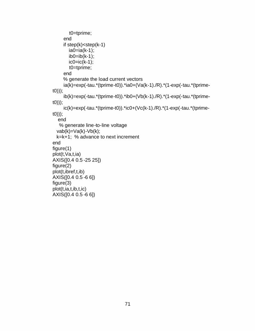
71
t0=tprime; end if step(k)<step(k-1) ia0=ia(k-1); ib0=ib(k-1); ic0=ic(k-1); t0=tprime; end % generate the load current vectors ia(k)=exp(-tau.*(tprime-t0)).*ia0+(Va(k-1)./R).*(1-exp(-tau.*(tprime-t0))); ib(k)=exp(-tau.*(tprime-t0)).*ib0+(Vb(k-1)./R).*(1-exp(-tau.*(tprime-t0))); ic(k)=exp(-tau.*(tprime-t0)).*ic0+(Vc(k-1)./R).*(1-exp(-tau.*(tprime-t0))); end % generate line-to-line voltage vab(k)=Va(k)-Vb(k); k=k+1; % advance to next increment end figure(1) plot(t,Va,t,ia) AXIS([0.4 0.5 -25 25]) figure(2) plot(t,ibref,t,ib) AXIS([0.4 0.5 -6 6]) figure(3) plot(t,ia,t,ib,t,ic) AXIS([0.4 0.5 -6 6])

72
THIS PAGE INTENTIONALLY LEFT BLANK
73
LIST OF REFERENCES
[1] “Advanced Electrical Power Systems Thrust,” Office of Naval Research website, www.onr.navy.mil, last accessed 30 May 2004.
[2] Paul Fillmore, “Design, construction, and testing of a hysteresis controlled dc-ac power converter for paralleling,” Master’s thesis, Naval Postgraduate School, Monterey, California, 2003.
[3] Ned Mohan, Tore M. Undeland, and William P. Robbins, Power Electron-ics, 3rd Edition, pp. 40-42, 204-239, John Wiley and Sons, Inc., Hoboken, New Jersey, 2003.
[4] Shoji Fukuda and Masayuki Kitano, “Control strategy for a three-phase series-connected hybrid inverter system,” Proc. 2001 IEEE 32nd Annual Power Electronics Specialists Conference, Vol. 2, pp. 968-973, IEEE Press, New York, 2001.
[5] Andrzej M. Trzynadlowski, Niculina Patriciu, Frede Blaabjerg, and John K. Pedersen, “A hybrid, current-source/voltage-source power inverter circuit,” IEEE Transactions on Power Electronics, Vol. 16, No. 6, pp. 866-871, 2001
[6] Adel S. Sedra and Kenneth C. Smith, Microelectronic Circuits, 4th Edition, pp. 980-982, Oxford University Press, New York, 1998.
[7] Robert F. Coughlin and Frederick F. Driscoll, Operational Amplifiers and Linear Integrated Circuits, 5th Edition, pp. 139-140, Prentice Hall, Upper Saddle River, New Jersey, 1998.
[8] Robert Crowe, “Design, construction, and testing of a reduced-scale cas-caded multi-level converter,” Master’s thesis, Naval Postgraduate School, Mon-terey, California, 2003.
[9] Toshiba America Electronic Components, Inc., “IGBT New Products Guide,” pp. 134-135, 1995.

74
[10] Paul C. Krause, Oleg Wasynczuk, and Scott D. Sudhoff, Analysis of Elec-tric Machinery and Drive Systems, 2nd Edition, pp. 481-494, IEEE Press, New York, 2002.

75
INITIAL DISTRIBUTION LIST
1. Defense Technical Information Center Ft. Belvoir, Virginia
2. Dudley Knox Library Naval Postgraduate School Monterey, California
3. Marine Corps Representative Naval Postgraduate School Monterey, California
4. Director, Training and Education, MCCDC, Code C46 Quantico, Virginia
5. Director, Marine Corps Research Center, MCCDC, Code C40RC Quantico, Virginia
6. Marine Corps Tactical Systems Support Activity (Attn: Operations Officer) Camp Pendleton, California
7. Dr. Robert Ashton, Department of Electrical and Computer Engineering Code EC/Ah Naval Postgraduate School
Monterey, California 8. Dr. Xiaoping Yun, Department of Electrical and Computer Engineering
Code EC/Yx Naval Postgraduate School
Monterey, California 9. Dr. John Powers, Chairman, Department of Electrical and Computer Engineering
Code EC Naval Postgraduate School Monterey, California
10. Major Terence H. White Stafford, Virginia