Embed Size (px)
DESCRIPTION
learn about nano
Citation preview


P1: RTJ
GGBD159FM GR3880/Mongillo Top Margin: 5/8in Gutter Margin: 3/4in September 25, 2007 16:1
Nanotechnology 101

P1: RTJ
GGBD159FM GR3880/Mongillo Top Margin: 5/8in Gutter Margin: 3/4in September 25, 2007 16:1
Recent Titles in theScience 101 Series
Evolution 101Janice Moore and Randy Moore
Biotechnology 101Brian Robert Shmaefsky
Cosmology 101Kristine M. Larsen
Genetics 101Michael Windelspecht
Human Origins 101Holly M. Dunsworth

P1: RTJ
GGBD159FM GR3880/Mongillo Top Margin: 5/8in Gutter Margin: 3/4in September 25, 2007 16:1
Nanotechnology 101
John Mongillo
Science 101
GREENWOOD PRESSWestport, Connecticut � London

P1: RTJ
GGBD159FM GR3880/Mongillo Top Margin: 5/8in Gutter Margin: 3/4in September 25, 2007 16:1
Library of Congress Cataloging-in-Publication Data
Mongillo, John F.Nanotechnology 101 / John Mongillo.
p. cm. – (Science 101, ISSN 1931-3950)Includes bibliographical references and index.ISBN–13: 978–0–313–33880–9 (alk. paper)1. Nanotechnology–Popular works. I. Title.T174.7.M66 2007620′.5–dc22 2007029805
British Library Cataloguing in Publication Data is available.
Copyright C© 2007 by John Mongillo
All rights reserved. No portion of this book may bereproduced, by any process or technique, without theexpress written consent of the publisher.
Library of Congress Catalog Card Number: 2007029805ISBN-13: 978–0–313–33880–9ISSN: 1931-3950
First published in 2007
Greenwood Press, 88 Post Road West, Westport, CT 06881An imprint of Greenwood Publishing Group, Inc.www.greenwood.com
Printed in the United States of America
The paper used in this book complies with thePermanent Paper Standard issued by the NationalInformation Standards Organization (Z39.48–1984).
10 9 8 7 6 5 4 3 2 1
P1: RTJ
GGBD159FM GR3880/Mongillo Top Margin: 5/8in Gutter Margin: 3/4in September 25, 2007 16:1
Contents
Series Foreword xvPreface xviiAcknowledgments xxi
1. What Is Nanotechnology? 1Introduction 1What Is Nanotechnology? 1
Living with Nanoparticles 3Nano, Nano, Nano 3Nanotechnology, a Future Trillion Dollar Business 3Nanotechnology Will Develop in Stages 4Nanotechnology Products and Applications 4
Sporting Goods 4Car Paint and Car Waxes 6Antibacterial Cleansers 6Medical Bandages 6Apparel Industry 6Sunscreens and Cosmetics 7Organic Light-Emitting Displays or OLEDs 7
Future Applications of Nanotechnology 7Environment 7Solar Energy 7Fuel Cells 8Food and Agriculture 8Automobiles and Aeronautics 8Medical Applications 9
Lab-on-a-Chip 9

P1: RTJ
GGBD159FM GR3880/Mongillo Top Margin: 5/8in Gutter Margin: 3/4in September 25, 2007 16:1
vi Contents
The U.S. Government Invests in Nanotechnology Research 10Other Countries Are Also Investing in Nanotechnology
Research 10What Do Americans Think of Nanotechnology? 10Will Nanotechnology Be Used to Help People in
Developing Countries? 11The Nanotechnology Job Market 13
The Need for Workers 13Universities Offer Nanotechnology Youth Programs 13The Fields of Study That Influence Nanotechnology 16
Feature: Mechanical Engineering 17Major Nanotechnology Career Areas 17What Are the Risks of Nanotechnology? 19
NANOSAFE2 20National Institute for Occupational Safety and Health
(NIOSH) 20Nanotechnology Environmental and Health
Implications (NEHI) 20National Nanotechnology Initiative (NNI) 20Environmental Protection Agency (EPA) 21Center for Biological and Environmental
Nanotechnology (CBEN) 21The Center for Responsible Nanotechnology 21
Nano Interview: Professor Martin L. Culpepper, Ph.D.,Massachusetts Institute of Technology 21
Nano Activity: Cutting It Down to Nano 26
2. The Science of Nanotechnology 29What Is Matter? 29
Forms of Matter 29Properties of Matter 30
Properties of Matter Change at the Nanoscale 31Volume to Surface Area 33
Matter’s Smallest Particles: Matter Is Made Up ofElements 33
The Periodic Table of Elements 33Semiconductors 35
Smallest Part of An Element: The Atom 35Inside the Atom: Subatomic Particles 36
Neutrons and Protons 36Electrons 36Isotopes 37

P1: RTJ
GGBD159FM GR3880/Mongillo Top Margin: 5/8in Gutter Margin: 3/4in September 25, 2007 16:1
Contents vii
Models of the Atoms 37Early Atomic Theory by Empedocles and Democritus 38Atomic Number and Atomic Mass 39
Atoms and Molecules 39Molecules and Chemical Bonding 40
Ionic Bonding 40Covalent Bonds and Monomers 40
A Monomer 41From Monomers to Polymers 41
Polymers and Nanotechnology 42Polymer-Based Nanosponges 42Polymer Solar Cells 43
A Unique Class of Synthetic Polymers, Dendrimers 43Dendrimers and Drug Delivery 43
Molecular Self-Assembly and Nanofabrication 44Soap Bubbles Self-Assemble 45Using the Self-Assembly Strategy to Make Products 45Other Applications of Molecular Self-Assembly 46
Self-Assembly in Medicine 46NanoSonic, Inc. 47
Nano Interview: Dr. Richard Claus, President of Nanosonic 48Nano Activity: Nanotechnology Demonstration Kit from
Nanosonic 50
3. The Nanotechnology Tool Box 55Optical Microscopes 55Scanning Probe Microscopes 56Surface Area to Volume at the Nanoscale 56
Scanning Tunneling Microscopes (STM) 57How Does the STM Work? 57
Atomic Force Microscopes (AFM) 57How Does the AFM Work? 58The Advantages of AFM 60AFM Tips 61
Magnetic Force Microscopes 61Interview: Nathan Unterman 61Electron Microscopes 63
A Scanning Electron Microscope 63Ernst Abbe 63
The Transmission Electron Microscope 64How Does the TEM Work? 64
Scanning Electron Microscope 65

P1: RTJ
GGBD159FM GR3880/Mongillo Top Margin: 5/8in Gutter Margin: 3/4in September 25, 2007 16:1
viii Contents
Hitachi Tabletop Microscope 66Nanofabrication Cleanroom Facilities 66Scanning Electron Microscopes and Photolithography 67Nano-Imprint Lithography 68
Dip Pen Nanolithography 68Thermal Dip Pen Nanolithography 69
NASA Virtual Lab 69Nanomanipulators 70Nanofabrication 70Nano Interview: Associate Professor Dean Campbell,
Ph.D., Bradley University 71Nano Activity: Modeling a Scanning Probe
Microscope 74
4. Carbon Nanotubes, Nanowires, and Nanocrystals 79The Element Carbon 79
Products Made from Carbon 80Some Uses of Carbon 80Different Forms of Carbon 81
Diamond 82Fullerenes and Nanotechnology 82Buckyballs 83
Applications of Buckyballs 83Carbon Nanotubes 83
Two Types of Nanotubes 85How are Carbon Nanotubes Made? 86
Laser Ablation 86Electric Arc Discharge 86Chemical Vapor Deposition (CVD) 86
Applications of Carbon Nanotubes 86Flat Panel Display Screens 88Nanoscale Electronics and Carbon Nanotubes 88
AFM Probe Tips 90Hydrogen Fuel Cells and Nanotubes 90Actuators/Artificial Muscles 90Nanotechnology in Chemical Sensors 91Carbon Nanotubes and NASA 92
NASA Space Elevator 92Not All Nanotubes are Carbon 92Nanowires, Nanocrystals, and Quantum Dots 93
Nanowires 93Production of Nanowires 93

P1: RTJ
GGBD159FM GR3880/Mongillo Top Margin: 5/8in Gutter Margin: 3/4in September 25, 2007 16:1
Contents ix
Nanocrystals 93Quantum Dots 94
Quantum Dots and Cancer 95Quantum Dots for Solar Cells 95
Nanoshells 96Nano Interview: Professor Timothy Sands, Ph.D., Purdue
University 96Nano Activity: Building Buckyballs, a NASA Explores Activity 100
5. Nanotechnology in Medicine and Health 103Cardiovascular Diseases 103
What Causes Cardiovascular Diseases? 104Nanoparticles Break Down Blood Clots 105Heart Stents and Nanotechnology 105
Cancer Detection and Diagnosis 106Cancer 106Cancer and Nanoshells 107Cancer and Gold Nanoparticles 107Breast Cancer and Nanoparticles 108
Nano Interview Dr. Edith Perez 109Cancer and Dendrimers 111Cancer and Cantilevers 112Cancer and Quantum Dots 112Cervical Cancer and Quantum Dots 112The Targeted Nano-TherapeuticsTM (TNTTM) System 113
Diabetes and Nanotechnology 113Nanorobots and Diabetes 114Biosensors for Diabetes 114Diabetes Research Continues 114
Tattoos for Diabetes 115Implants and Prosthetics 115Nanotechnology and Burn Victims 116Diagnosis and Therapy 116
Molecular Imaging Diagnosis 117Lab-on-a-Chip Diagnosis 117
Drug Delivery Using Nanoparticles 117Advanced Drug Delivery Systems and Lab-on-a-Chip 118
Nanotechnology Fights Infections 119Pharmaceutical Nanotechnology Research 119Nano Interview: Matt Boyas and Sarah Perrone 120
6. The Business of Nanotechnology 125Nanotechnologies in Businesses 125

P1: RTJ
GGBD159FM GR3880/Mongillo Top Margin: 5/8in Gutter Margin: 3/4in September 25, 2007 16:1
x Contents
Sporting Goods Equipment 125Baseball Bats 126Tennis Rackets 126Nano Golf Balls 126Skis and Nanofibers 126
Chewing Gum and Nanocrystals 127Apparel Industry 128
Nanotechnology in Cleaner Clothes 128Nanotechnology Socks 128
Cosmetics 129Sunscreens and Skin Cancer 129
Appliances 130Nano Silver Seal Refrigerator 130Flat-Plane Display Screens 131The Business of Air Purifiers 131
Electronics and Computers 131Automobile/Vehicle Industry 132
Auto Catalytic Converters 132Automobile Paint and Waxes 133
Aircraft Potential and Metal Rubber 134Paint and Other Water Resistance Coatings 134
Paints and Anti-Graffiti Coating 134Removing Windshield Fog 135Self-Cleaning Glass 135Antibacterial Cleansers 135Medical Bandages 135Solar Energy: Photovoltaic Cells 136Battery Technology 137
Virus-Assembled Batteries 137Long-Lasting Batteries 137
The Business of Building Atomic Force Microscopes 138Nano Interview: Dr. Alyssa Wise and Dr. Patricia Schank
(NanoSense Team) and Dr. Brent Macqueen(Nanoscientist) 139
Nano Activity: Sunscreens and Sunlight Animations,Adapted from SRI International’s Nanosense Unit 142
7. Nanotechnology for Food, Agriculture, Livestock,Aquaculture, and Forestry 147United States Department of Agriculture 147Food Packaging: A Major Goal Using Nanotechnology
Methods 148

P1: RTJ
GGBD159FM GR3880/Mongillo Top Margin: 5/8in Gutter Margin: 3/4in September 25, 2007 16:1
Contents xi
Nano Plastic Packaging 148New Kinds of Bottles 149
Foodborne Diseases 149Listeria Monocytogenes in Food 149Salmonella Ilnesses from Food 149
Nanosensors for Foodborne Contamination 151Using Food Packaging Sensors in Defense and Security
Applications 152Other Kinds of Sensors: The Electronic Nose and The
Electronic Tongue 152The Electronic Nose (e-nose) Technology 152The Electronic Tongue Technology 153
Nano Bar Codes Detect Foodborne Diseases 153Agriculture and Nanotechnology 154Biosensor Detects Herbicides on the Farm 154
Nanoscale Herbicides 155A Food Safety Issue 155Atomic Force Microscopy and Food Research 156Sustainable Watering of Crops 156Livestock Diseases 157Biochips for Disease Detection in Livestock 157
Biochips for Animal Breeding 158Nanosensors to Track Livestock 158Nanotechnology in Aquaculture and Fish Farming 158
Environmental Concern of Aquaculture 159Cleaning Fish Ponds with Nanotechnology Devices 159DNA Nanovaccines Using Nanocapsules and Ultrasound
Methods 159Forest Product Industry and Nanotechnology 159Ensuring Nanotechnologies in Food Production to Be Safe 160Nano Interview: Professor Makarand (MAK) Paranjape,
Ph.D., Georgetown University 160Nano Activity: Food Packaging 166
8. Nanotechnology for a Sustainable Environment 169Water Pollution and Nanotechnology 169Nanotechnology and Safer Drinking Water 170
Cleaning Up Arsenic 170The Element Arsenic 170Nanotechnology and Water Filters 171
Drinking Water from the Ocean 172

P1: RTJ
GGBD159FM GR3880/Mongillo Top Margin: 5/8in Gutter Margin: 3/4in September 25, 2007 16:1
xii Contents
Reverse Osmosis 172A New Kind of Reverse Osmosis 172Water Pollution: Using the Atomic Force Microscope to
Study Water Pollution 173Groundwater Pollutants 173Groundwater Cleanup 173
Iron Nanoparticles May Be Effective in Cleaning UpWaste Sites 174
Cleaning Up Organic Pollutants Using Nanotechnology 175TCE Cleanup with Gold Nanoparticles 175
Cleaning Up Nuclear Waste Sites 176Air Pollution 176
Titanium Dioxide and Clean Air 177What Is Titanium Dioxide? 177
Environmental Protection Agency and Department ofEnergy 178
Environmental Protection Agency 178Department of Energy 179
Nanotechnology and Energy Sources 179Solar Photovoltaic Cell (PV) 179
Quantum Dots for Solar Cells 180Hydrogen Fuel Cells 181
Fuel Cells and the Automobile Industry 181The Problem with Fuel Cells 182
Emerging Nanotechnologies and Risks 183Nano Interview: Professor Paul G. Tratnyek, Ph.D., Oregon
Health & Science University’s OGI School of Science& Engineering 183
Nano Activity: Discovering the Properties of Ferrofluids(Teacher Supervision Advised) 190
Materials You Need 190Where to Buy Ferrofluids 190
9. Nanotechnology Projects and the United StatesGovernment 193National Nanotechnology Institute 193The National Nanotechnology Initiative (NNI) and
Federal Agencies 195National Aeronautics and Space Administration (NASA) 195
Lab-on-a-Chip 195Spacecraft 196

P1: RTJ
GGBD159FM GR3880/Mongillo Top Margin: 5/8in Gutter Margin: 3/4in September 25, 2007 16:1
Contents xiii
A Self-Repair Spacecraft 197Spacecraft Recycling 197Improvements in NASA Spacesuits 197NASA Space Elevator 197
Carbon Nanotubes and the Space Elevator. 197National Science Foundation 198
National Science Foundation Classroom Resources 199National Institute of Standards and Technology (NIST) 199The Food and Drug Administration (FDA) 200Department of Defense (DOD) 200Department of Homeland Security 201
Underwater Sensor Networks 202The Mapleseed: A Nano Air Vehicle for Surveillance 202
Safety in Nanotechnology: The National Institute forOccupational Safety and Health (NIOSH) 202
Nano Interview: Laura Blasi, Ph.D., and NASA’s VirtualLab 203
Nano Activity: NASA Virtual Lab. Try It! 207Animation of Atomic Force Microscopy Basics 208
10. Colleges and Schools and Nanotechnology 211An Interview with Dr. Nancy Healy, Education Coordinator
of the National Nanotechnology InfrastructureNetwork (NNIN) 212
National Science Teachers Association and ExploraVision 218ExploraVision Project 219ExploraVision Project: Appy-Bot, Norma L. Gentner 219Other Toshiba/NSTA ExploraVision Winners 222
La Jolla, California 222St. Louis, Missouri 222
Colleges Motivate Students in Nanotechnology 222NanoDay at Northwestern 223
Northwestern University and Materials World Modules 223Penn State Nanotech Camps 223Rice University: The NanoKidsTM 224University of California, Santa Barbara: Chip Camp 224College of Nanoscale Science and Engineering (CNSE),
University of Albany 225Cornell University 225The University of Wisconsin-Madison 226Arizona State University 226

P1: RTJ
GGBD159FM GR3880/Mongillo Top Margin: 5/8in Gutter Margin: 3/4in September 25, 2007 16:1
xiv Contents
North Carolina State University and the University ofNorth Carolina, Chapel Hill 226
SRI International: NanoSense 226Nanotechnology in Museums and Traveling Exhibits 227
Making Things Smaller 227It’s a Nano World and Too Small to See Exhibits 227Lawrence Hall of Science 229
High School Programs in Nanotechnology 229Nanotechnology Information and Sites for Teachers 230Nano Interview: Ms. Renee DeWald, Toshiba/NSTA
ExploraVision, Fighting Cancer with Nano-Shells 230Nano Activity: Nanotechnology Consumer Products 232
Appendix A: Bibliography 235Appendix B: Companies in Nanotechnology Research and Development 238Appendix C: Nanotechnology Web Sites 246Appendix D: Nanotechnology Videos and Audios 250Appendix E: Some Important Events in Nanotechnology History 257Appendix F: National Science Education Standards, Content
Standards 259Appendix G: Colleges and Museums 261
Glossary 265Index 271

P1: RTJ
GGBD159FM GR3880/Mongillo Top Margin: 5/8in Gutter Margin: 3/4in September 25, 2007 16:1
Series Foreword
What should you know about science? Because science is so central tolife in the twenty-first century, science educators believe that it is essen-tial that everyone understand the basic foundations of the most vital andfar-reaching scientific disciplines. Science 101 helps you reach that goal—this series provides readers of all abilities with an accessible summaryof the ideas, people, and impacts of major fields of scientific research.The volumes in the series provide readers—whether students new to thescience or just interested members of the lay public—with the essentialsof a science using a minimum of jargon and mathematics. In each vol-ume, more complicated ideas build upon simpler ones, and conceptsare discussed in short, concise segments that make them more easily un-derstood. In addition, each volume provides an easy-to-use glossary andannotated references and resources of the most useful and accessibleprint and electronic resources that are currently available.

P1: RTJ
GGBD159FM GR3880/Mongillo Top Margin: 5/8in Gutter Margin: 3/4in September 25, 2007 16:1

P1: RTJ
GGBD159FM GR3880/Mongillo Top Margin: 5/8in Gutter Margin: 3/4in September 25, 2007 16:1
Preface
OVERVIEW
Nanotechnology: A 21st-Century Technology
Nanotechnology is the ability to observe, measure, manipulate, andmanufacture things at the nanometer scale, the size of atoms andmolecules.
The National Science Foundation predicts that the global market-place for goods and services using nanotechnologies will be worth atrillion dollars by 2015. In the same year, career opportunities in thisfast-paced technology will require 2–5 million semiskilled and skilledemployees worldwide. Nanotechnology has the potential to affect ev-erything from the clothes we wear, to the energy we use, to the way wedetect and treat cancer and other diseases.
Nanotechnology 101 is a reference book and an excellent research toolfor developing a working knowledge of basic nanotechnology conceptsand topics. Besides the potential benefits of nanotechnology, the legal,ethical, and social issues are also addressed.
In recent years, there have been several nanotechnology surveys thathave found that a majority of the adults know little or nothing aboutnanotechnology. Therefore, in an effort to make the book more ac-cessible and appealing to a broad range of readers, Nanotechnology 101incorporates many features and enhancements that include:
� Current Nanotech Topics. This book provides all of the basic conceptsand topics of nanotechnology. In its comprehensive, easy-to-read format,Nanotechnology 101 covers nanotechnology’s influence in medicine, engi-neering, economics, electronics, communications, energy, environment,transportation, space travel, and homeland security.

P1: RTJ
GGBD159FM GR3880/Mongillo Top Margin: 5/8in Gutter Margin: 3/4in September 25, 2007 16:1
xviii Preface
� Bibliography. An excellent listing of reading materials at the end of eachchapter and in the appendix is provided.
� Interviews. This book also features more than 15 interviews with peoplewho work and study in the nanotechnology field. The interviews includea nanotechnology business owner, an electrical engineer, a physics pro-fessor, an environmentalist, a chemistry teacher, and two high schoolstudents who were winners of an NSTA nanotechnology project.
� Companies and Products. General information and Web sites for morethan 100 companies who are involved in cutting-edge nanotechnologyresearch and nanofabrication have been presented to the reader. Some ofthese companies include IBM, Intel, Samsung, Eastman Kodak, Dupont,and Hitachi High Technologies.
� Career Information. It encourages young people to explore the possibil-ities of a career in the nanotechnology field by providing resources theycan contact to learn more about career opportunities in the field. As anexample, Penn State provides a free CD, Careers in Nanofabrication.
� Video Sources. To enhance the text, Nanotechnology 101 provides morethan 80 nanotechnology video Web sites. As an example, Is NanotechnologyGoing to be the Next Industrial Revolution? Conversations in Science, MadisonMetropolitan School District, UW-Madison Interdisciplinary EducationGroup. If you would like to view the video go to: http://mrsec.wisc.edu/Edetc/cineplex/MMSD/nano5.html
� Hands-on Activities and Suggested Projects. There are suggestions andopportunities for students and teachers to explore nano activities. As anexample, students can make a nanometer ruler, construct a Buckyballmodel, and build a LEGO R© model of an atomic force microscope. Wantto know how a scanning electron microscope works? Students can accessNASA’s electron microscope virtual lab Web site.
� Government and Nongovernment Resources. All of the major govern-ment agencies that are conducting nanotechnology research and fundingare included. Familiar names include Department of Energy, Environ-mental Protection Agency, and NASA. Many nongovernment groups arelisted as well. This list includes such organizations as, Foresight Institute,Nanotech Institute, Nano Science and Technology Institute, NanoBusi-ness Alliance, Institute of Technology, and Nanotech.
� Nanotechnology Timeline of Events. The timeline provides an opportu-nity to trace some of the important events of the history of nanotechnol-ogy.
� University and College Resources. Nanotechnology 101 includes nanotechresource links and Web sites from more than 20 colleges and universitiesthat provide nanotechnology educational and outreach programs devotedto middle school or high school students. By contacting these college sites,

P1: RTJ
GGBD159FM GR3880/Mongillo Top Margin: 5/8in Gutter Margin: 3/4in September 25, 2007 16:1
Preface xix
students and teachers can access interactive activities, lesson plans, onlineexhibits, experiments, games, and video broadcasts.
� National Science Education Standards. The content in the book providesa close alignment with the National Science Education Standards. Nanotech-nology is not a traditional discipline, but rather a combination of dis-ciplines involving physics, chemistry, biology, mathematics, engineering,and technology. Nanotechnology 101 provides information in the appendixthat links nanotechnology concepts with those science education stan-dards in each of the major science fields.
RICHARD E. SMALLEY (1943–2005)
To many people, Richard Smalley was the foremost leader in nan-otechnology. He has often been noted as the “Father of Nanotechnol-ogy.”
Richard Smalley was a Rice University professor who won a NobelPrize in chemistry in 1996. He is well known for his work with carbonnanotubes (known as the “Buckyballs”).
In the spring of 1999, Professor Smalley addressed the Senate Subcom-mittee on Science, Technology, and Space. Testifying at the meetings,he had called for congressional support of a National NanotechnologyInitiative (NNI) that could double U.S. Federal funding for nanoscaleresearch and development efforts over the next 3 years, to about $460million.
In 1999, while Professor Richard Smalley was testifying before theCongress, he had also been fighting leukemia for over a year. At onemeeting, he had the opportunity to speak about the medical applicationsof nanotechnology. Here is an excerpt of what he had to say.
I sit before you today with very little hair on my head. It fell out a few weeksago as a result of the chemotherapy I’ve been undergoing to treat a type ofnon-Hodgkin’s lymphoma. While I am very optimistic, this chemotherapy is avery blunt tool. It consists of small molecules, which are toxic—they kill cellsin my body. Although they are meant to kill only the cancer cells, they kill haircells too, and cause all sorts of other havoc.
Now, I’m not complaining. Twenty years ago, without even this crudechemotherapy, I would already be dead. But 20 years from now, I am confidentwe will no longer have to use this blunt tool. By then, nanotechnology willhave given us specially engineered drugs, which are nanoscale cancer-seekingmissiles, a molecular technology that specifically targets just the mutant can-cer cells in the human body and leaves everything else blissfully alone. . . .
I may not live to see it. But, with your help, I am confident it will happen.Cancer—at least the type that I have—will be a thing of the past.

P1: RTJ
GGBD159FM GR3880/Mongillo Top Margin: 5/8in Gutter Margin: 3/4in September 25, 2007 16:1
xx Preface
Richard Smalley died of non-Hodgkin’s lymphoma on October 2005.In 1999, the Rice University Center for Nanoscale Science and Tech-
nology (CNST) was renamed the Richard E. Smalley Institute forNanoscale Science and Technology in his honor.
Note: Non-Hodgkin’s lymphoma (NHL) is the nation’s sixth leading cause of cancerdeath. The American Cancer Society predicted that there would be about 6,300 newcases of NHL in this country in 2007. About 18,000 people die of this disease eachyear.

P1: RTJ
GGBD159FM GR3880/Mongillo Top Margin: 5/8in Gutter Margin: 3/4in September 25, 2007 16:1
Acknowledgments
The author wishes to acknowledge and express the contribution of gov-ernment and nongovernment organizations and companies. A specialthanks to the following people who provided resources, photos, and in-formation: Dr. Laura Blasi at Saint Leo University, Florida; Mr. Paul Oc-tavio Boubion, 8th grade physical science teacher at the Carl H. LorbeerMiddle School in California; high school students, Matt Boyas and SarahPerrone who attend the Upper St. Clair School District in Pennsylva-nia; Associate Professor Dean Campbell, Ph.D. at Bradley Universityin Peoria, Illinois; Dr. Richard Claus, president of NanoSonic Inc. lo-cated in Virginia; Dr. Martin L. Culpepper at Massachusetts Institute ofTechnology in Massachusetts; Renee DeWald, chemistry teacher at theEvanston Township High School in Illinois; Norma L. Gentner, Enrich-ment Teacher at Heritage Heights Elementary in Amherst, New York;Dr. Nancy Healy, Education Coordinator of the National Nanotechnol-ogy Infrastructure Network (NNIN) in Georgia; Catherine Marcotte,science teacher, ForwardVIEW Academy in Rhode Island; Patricia Palaz-zolo, Gifted Education Coordinator, for the Upper St. Clair School Dis-trict in Pennsylvania; Dr.Makarand Paranjape at Georgetown UniversityWashington, DC; Edith A., Perez, Medical Doctor and a Professor ofMedicine at the Mayo Medical School in Florida; Professor TimothyD. Sands,Ph.D. at Purdue University; Professor Paul G. Tratnyek, Ph.D.at Oregon Health & Science University’s OGI School of Science &Engineering; Nathan A. Unterman, physics teacher at the GlenbrookNorth High School in Illinois; Dr. Alyssa Wise and Dr. Patricia Schank(NanoSense team) and Dr. Brent MacQueen at SRI International inCalifornia.

P1: RTJ
GGBD159FM GR3880/Mongillo Top Margin: 5/8in Gutter Margin: 3/4in September 25, 2007 16:1
xxii Acknowledgments
Many thanks to Amy Mongillo and Dan Lanier who provided spe-cial assistance in reviewing topics and offering suggestions. In ad-dition, Cynthia Sequin of Purdue Public Relations, Catherine Mc-Carthy, Grants Project Director of Sciencenter, Cornell University, IBM,Konarka Technologies, Oak Ridge National Laboratory, and HitachiHigh-Technologies ( Japan) who provided technical assistance in ac-quiring photos for the book.
P1: 000
GGBD159C01 GR3880/Mongillo Top Margin: 5/8in Gutter Margin: 3/4in September 25, 2007 16:2
1
What IsNanotechnology?
INTRODUCTION
A patron at a local restaurant spills coffee on his trousers. The liquidbeads up and rolls off without leaving a spot on his clothing.
The U.S. Golf Association suggests that golfers can now use new golfballs that fly straighter, with less wobble, than normal golf balls.
A woman is using a new variety of canola oil in preparing her meals.The oil contains tiny particles that block cholesterol from entering herbloodstream.
Walking down a street in London, England, a pedestrian suddenlysmells that the air is cleaner. The sidewalk is treated with a specialproduct that breaks down harmful pollutants in the air.
The air purifying pavement, the new golf balls, the nonstain pants, arejust some of the examples of products produced by nanotechnology, akey technology for the 21st century. Nanotechnology offers cutting-edgeapplications that will revolutionize the way we detect and treat disease,monitor and protect the environment, produce and store energy, im-prove crop production and food quality, and build complex structuresas small as an electronic circuit or as large as an airplane.
WHAT IS NANOTECHNOLOGY?
Nanotechnology is the ability to observe, measure, manipulate, andmanufacture things at the nanometer scale. A nanometer (nm) is anSI (Systeme International d’Unites) unit of length 10−9 or a distance ofone-billionth of a meter. That’s very small. At this scale, you are talkingabout the size of atoms and molecules.
To create a visual image of a nanometer, observe the nail on yourlittle finger. The width of your nail on this finger is about 10 million

P1: 000
GGBD159C01 GR3880/Mongillo Top Margin: 5/8in Gutter Margin: 3/4in September 25, 2007 16:2
2 Nanotechnology 101
Table 1.1 Some Common Objects in Nanometers
How Many Nanometers? Approximately
The Width of an Atom 1 nanometer (nm)The Width Across a DNA Molecule 2 nanometersThe Width of a Wire in a Computer 100 nanometersThe Wavelength of Ultraviolet Light 300 nanometersThe Width of a Dust Particle 800 nanometersThe Length of Some Bacteria 1,000 nanometersThe Width of a Red Blood Cell 10,000 nanometersThe Width of a Hair 75,000 to 100,000 nanometersThe Width Across a Head of a Pin 1,000,000 nanometersThe Width Across the Nail of a Little
Finger10,000,000 nanometers
nanometers across. To get a sense of some other nano-scaled objects, astrand of human hair is approximately 75,000 to 100,000 nanometersin diameter. A head of a pin is about a million nanometers wide and itwould take about 10 hydrogen atoms end-to-end to span the length ofone nanometer.
The word “nanotechnology” was first introduced in the late 1970s.While many definitions for nanotechnology exist, most groups use theNational Nanotechnology Initiative (NNI) definition. The NNI callssomething “nanotechnology” only if it involves all of the following:
� Research and technology development at the atomic, molecular, or macro-molecular levels, in the length scale of approximately 1 to 100-nanometerrange.
� Creating and using structures, devices, and systems that have novelproperties and functions because of their small and/or intermediatesize.
� Ability to control or manipulate on the atomic scale.
See Chapter 8 for more information about the National NanotechnologyInitiative.
Please note that nanotechnology is not merely the study of smallthings. Nanotechnology is the research and development of materi-als, devices, and systems that exhibit physical, chemical, and biologicalproperties. These properties can be different from those found at largerscales—those that are more than 100 nanometers.
P1: 000
GGBD159C01 GR3880/Mongillo Top Margin: 5/8in Gutter Margin: 3/4in September 25, 2007 16:2
What Is Nanotechnology? 3
Living with Nanoparticles
You live with nanoparticles every day. In a normal room, there areabout 15,000 nanoparticles per cubic centimeter in the air. If youare taking a walk in the forest, you will be in an environment wherethere will be about 50,000 nanoparticles per cubic centimeter. In alarge city, there can be about 100,000 nanoparticles per cubic centi-meter (cm3).
NANO, NANO, NANO
In this chapter as well as in the others, we will be using terms,such as nanostructures, nanodevices, nanoparticles, nanoscale, nano-medicine, nanowires, nanotubes, nanoengineering, and so forth.
� If you have time, you may want to watchthe video, What is Nanotechnology? Pro-fessor Wendy Crone narrates the video.http://www.sciencedaily.com/videos/2006-06-11/
The prefix, “nano,” is usedto indicate a tool, an enter-prise, a particle, a pheno-menon, a project, or a man-ufactured item operating onor concerned with a scale atone billionth of a meter.
NANOTECHNOLOGY, A FUTURE TRILLIONDOLLAR BUSINESS
Making products at the nanometer scale is and will become a bigeconomy for many countries. By 2015, nanotechnology could be a
Did you know?Nano is derived from the Greek word meaning“dwarf.”
$1 trillion industry. Mean-while, according to the Na-tional Nanotechnology Ini-tiative (NNI), scientists willcreate new ways of making
Did you know?Even though you cannot see nanometer-sized par-ticles, you can smell some of them. As an example,the particles (molecules) in the air that float from acake baking in an oven are less than a nanometer insize. They are suspended in the air because gravitydoes not have much of an effect on them, owing totheir small size and mass. As the particles dispersearound the room, they reach our noses and we cansmell them less than a nanometer away.
structural materials that willbe used to build productsand devices atom-by-atomand molecule-by-molecule.These nanotechnology ma-terials are expected to bringabout lighter, stronger,smarter, cheaper, cleaner,and more durable products.

P1: 000
GGBD159C01 GR3880/Mongillo Top Margin: 5/8in Gutter Margin: 3/4in September 25, 2007 16:2
4 Nanotechnology 101
NANOTECHNOLOGY WILL DEVELOP IN STAGES
Dr. Mihail Roco is a senior advisor on nanotechnology to the NationalScience Foundation (NSF) and coordinator of the NNI. Dr. Roco be-lieves that nanotechnology will have several phases of development. Hestates that we are now in the second phase. The first one consisted of us-ing nanostructures, simple nanoparticles, designed to perform one task.The second phase started in 2005. In the second phase, researchers havediscovered ways to precisely construct nanoscale building blocks. Theblocks can be assembled into flat or curved structures such as bundles,sheets, and tubes. These structures hold promise for new and power-ful drug delivery systems, electronic circuits, catalysts, and light energysources.
By 2010, Dr. Roco says, the third phase will arrive, featuring nanosys-tems with thousands of interacting components. A few years after that,the first “molecular” nanodevices will appear. These devices will be com-posed of systems within systems operating much like a human cell works.
One of the main reasons why there is a lot more activity in producingnanotechnology products today than before is because there are nowmany new kinds of tools. These new tools consisting of special scan-ning electron microscopes and atomic force microscopes can measure,see, and manipulate nanometer-sized particles. See Chapter 3 for moreinformation about nanotechnology tools.
NANOTECHNOLOGY PRODUCTS AND APPLICATIONS
What kinds of nanoproducts are available now?More than $32 billion in products containing nanomaterials were
sold globally in 2005. As was stated earlier, the global marketplace forgoods and services using nanotechnologies will grow to $1 trillion by2015. However, other financial experts predict that the marketplace fornanoproducts will reach $2.6 trillion in manufactured goods by 2014.
Presently, there are more than 200 companies that market and sellproducts using nanotechnology applications. Many of these companiesproduce much of the 700 or so nanoproducts that are currently availablein the U.S. marketplace. Let’s review a few examples of nanoproductsthat are available today.
Sporting Goods
Special nanoparticles made of carbon are used to stiffen areas of theracquet head and shaft. The particles are 100 times more rigid than steeland 6 times lighter. The new composite hockey stick developed is more

P1: 000
GGBD159C01 GR3880/Mongillo Top Margin: 5/8in Gutter Margin: 3/4in September 25, 2007 16:2
Figure 1.1 Scale of Things. (Courtesy of Jeff Dixon)

P1: 000
GGBD159C01 GR3880/Mongillo Top Margin: 5/8in Gutter Margin: 3/4in September 25, 2007 16:2
6 Nanotechnology 101
durable than other sticks because of the carbon nanotube epoxy matrix.Nano tennis balls coated internally with a nano-sized membrane, slowpressure drain without adding weight.
Car Paint and Car Waxes
There are now new kinds of automobile paints, developed from nan-otechnology, that have improved scratch-resistant qualities compared toconventional car paint. Nano car waxes, made with nano-sized polishingagents, provide a better shine due to its ability to fill-in tiny blemishes inautomotive paint finishes.
Antibacterial Cleansers
There are several antibacterial cleansers that use nanoemulsion tech-nology to kill pathogens. The cleansers are able to kill tuberculosis andbacteria while remaining nonflammable, noncorrosive, and nontoxic.The good news is that there are no harmful effects when using theseproducts.
Medical Bandages
Silver’s antibiotic properties have made the metal a popular treat-ment for wounds and burns. Special dressings for burns provide
Did you know?The cleansing power of silver was known in the daysof the Roman Empire, when silver coins were usedto purify water in jugs and containers for drinkingand cooking purposes.
antimicrobial barrier protec-tion using concentrations ofnano silver particles. Thesemedical bandages help skinto heal by preventing infec-tions during treatment. Thesilver-impregnated dressings
require fewer painful changings of dressings than previous silvertreatments.
Apparel Industry
Several clothing companies have marketed new brands of nonstainnanotechnology fabrics. The fabric resists spills from many types of fibers(cotton, synthetics, wool, silk, rayon, and polypropylene). The fabricalso repels a range of liquids including beverages and salad dressings.These fabrics keep the body cool and comfortable and have an antistatictreatment that reduces static cling from dog hair, lint, and dust. SeeChapter 6 for more information about nanotechnology fabrics.

P1: 000
GGBD159C01 GR3880/Mongillo Top Margin: 5/8in Gutter Margin: 3/4in September 25, 2007 16:2
What Is Nanotechnology? 7
Sunscreens and Cosmetics
Several cosmetic companies have already marketed a number of prod-ucts that include nanotechnology. The products include sunscreens, de-odorants, and antiaging creams. One sunscreen product uses zinc oxidenanoparticles that protects the skin but does not leave white marks onthe skin. However, more regulation of some of these products will beneeded because of the limited research that has been carried out in thisstill new field. See Chapter 6 for more information about sunscreens.
Organic Light-Emitting Displays or OLEDs
The OLEDs are ultrathin displays manufactured by sandwiching ex-tremely thin (often nano-sized) layers of organic polymer light-emittingmaterials between electrodes. These images are bright and viewable atwide angles. The displays are smaller and of lighter weight than tradi-tional LCD (liquid crystal display) displays—meaning they are ideallysuited to mobile electronics, such as digital cameras, cellular phones,and handheld computers.
FUTURE APPLICATIONS OF NANOTECHNOLOGY
What can we look for in future applications of nanotechnology?
Environment
Emerging nanotechnologies hold great promise for creating newmeans of detecting air pollutants, and cleaning polluted waste streamsand groundwater. A research group is now testing the use of magneticnanoparticles that can absorb and trap organic contaminants in water. Ifthe testing continually succeeds, the process can also be very effective incleaning up contaminated Superfund sites—hazardous and toxic wastesites—in the United States. See Chapter 8 for more information aboutthe environment.
Solar Energy
Researchers are making an effort to find a lower-cost source of house-hold energy for the nation’s future. They are exploring the creationof nanoscale devices on the molecular level that can convert sunlightinto electric current. Scientists have invented a plastic solar cell thatcan turn the sun’s power into electrical energy, even on a cloudy day.The plastic material uses nanotechnology and contains solar cells ableto harness the sun’s invisible, infrared rays. Like paint, the composite

P1: 000
GGBD159C01 GR3880/Mongillo Top Margin: 5/8in Gutter Margin: 3/4in September 25, 2007 16:2
8 Nanotechnology 101
can be sprayed onto other materials and used as a portable source ofelectricity. A sweater coated in the material could power a cell phone orother wireless devices.
However, the idea of using nanostructures to convert sunlight intoelectricity is still theoretical. The main concern is that the present costof electricity produced by solar cells is four times greater than electricityproduced by nuclear or fossil fuels. Many companies and governmentagencies are funding much research in solar projects, which indicatesthere is an increasing interest in this field by the scientific communityand corporations. See Chapter 8 for more information about solar cells.
Fuel Cells
Several companies are utilizing nanostructure technology to help de-velop high performance fuel cells for use in automobiles, portable con-sumer electronics such as laptop computers, cell phones, and digitalcameras. A fuel cell is an energy conversion device and alternative tobatteries that converts energy from a chemical reaction into electricityand heat. Fuel cells combine fuels such as hydrogen or methanol alongwith air and water to produce electrical power. Because their by-productsare heat and water, fuel cells are environmentally friendly. See Chap-ter 8 for more information about fuel cells.
Food and Agriculture
The ability to use nanotechnology will allow food companies to de-sign and provide food products that would be safer, cheaper, andmore sustainable than the foods today. Food companies will also useless water and chemicals in the preparation and production of foodproducts.
One food company had developed nanosensors that would be embed-ded in food packaging. A color change in the nanosensor would alertthe consumer if a food in the package had become contaminated or if ithad begun to spoil. Some companies are producing a plastic consistingof clay nanoparticles. The nanoparticles in the plastic are able to blockout oxygen, carbon dioxide, and moisture from spoiling fresh meatsand other foods. See Chapter 7 for more information about food andagriculture.
Automobiles and Aeronautics
Nanoscale powders and nanoparticles will be able to enhance thephysical properties of automobile, aircraft, watercraft, trains, and

P1: 000
GGBD159C01 GR3880/Mongillo Top Margin: 5/8in Gutter Margin: 3/4in September 25, 2007 16:2
What Is Nanotechnology? 9
spacecraft. Planes, trains, and automobiles will be lighter, faster, andmore fuel-efficient and constructed of lighter, stronger materials. Someof these lightweight materials will include aluminum bodies for automo-biles, brake systems for high-speed trains, and quieter aircraft engines.The stronger, lighter materials will help in energy efficiency and re-ducing mass and weight of finished products. See Chapter 6 for moreinformation about automobiles and aircraft.
Medical Applications
Many medical procedures could be handled by nanomachines thatrebuild arteries, rebuild bones, and reinforce bones. In cancer nan-otechnology research, scientists are testing and experimenting with newideas to diagnose, treat, and prevent cancer in the future.
One research medical team is using nanoshells to target cancer cells.Nanoshells are hollow silica spheres covered with gold. In animal test-ing, Naomi Halas’s research team at Rice University directed infraredradiation through tissue and onto the shells, causing the gold to super-heat and destroy tumor cells while leaving healthy ones intact. Humanclinical trials using gold nanoshells are slated to begin within a fewyears.
Another cancer research team has shown that the targeted goldnanoparticles combined with lasers can kill oral cancer cells. Oral can-cer is any cancerous tissue growth located in the mouth. Smoking andother tobacco use are associated with 70–80 percent of oral cancer cases.Thirty thousand Americans will be diagnosed with oral or pharyngealcancer this year. See Chapter 5 for more information about the medicalfield.
Lab-on-a-Chip
In other nano medical news, researchers are studying lab-on-a-chiptechnology. Lab-on-a-chip technology consists of a portable handhelddevice containing a simple computer chip that can diagnose and mon-itor the medical conditions of a patient. As an example, a tiny sampleof blood placed on the device could diagnose if the patient is diabetic.The lab-on-a-chip could be used for commercial, medical diagnostic ap-plications, such as an in-office test for strep throat, or modern in-homepregnancy tests.
NASA has customized lab-on-a-chip technology to protect future spaceexplorers. The lab-on-a-chip would be used to monitor the health of thecrew by detecting contaminants in the spacecraft.

P1: 000
GGBD159C01 GR3880/Mongillo Top Margin: 5/8in Gutter Margin: 3/4in September 25, 2007 16:2
10 Nanotechnology 101
THE U.S. GOVERNMENT INVESTS IN NANOTECHNOLOGYRESEARCH
Nanotechnology is expected to have large impact on many sectors ofthe world’s economy. A strong nanotechnology economy can lead to newproducts, new businesses, new jobs, and even new industries for manycountries. As a result, nanotechnology funding for research is growingrapidly all over.
In 2001, President Clinton requested a major new initiative in the 2002federal budget, called the National Nanotechnology Initiative (NNI).The budget included an increase of more than 200 million dollars forthe government’s investment in nanotechnology research and devel-opment. In December 2003, President Bush signed the Nanotechnol-ogy Research and Development Act, which authorized funding for nan-otechnology research and development (R&D) over 4 years, starting inFY 2005. This legislation puts into law programs and activities supportedby the National Nanotechnology Initiative.
The 2003 bill authorized nearly $3.7 billion for research and de-velopment programs coordinated among several federal agencies. Thelegislation also authorized public hearings and expert advisory panels,as well as the American Nanotechnology Preparedness Center to studythe emerging technology’s potential societal and ethical effects.
Other Countries Are Also Investing in Nanotechnology Research
The United States is not the only country to recognize the tremen-dous economic potential of nanotechnology. In 2007, the Russian gov-ernment planned to take its export revenues from oil and gas sales andinvest it in nanotechnology research and development. During the next3 years, Russia will invest more than $1 billion in nanotechnology so thatit can become less dependent on raw materials.
Brazil had a projected budget for nanoscience during 2004 to 2007that included creating three institutions, four networks, and recruiting300 scientists to work in nanotechnology research. Some of the Brazil-ian researchers are interested in the use of magnetic nanoparticles toremove oil from oil spills and then be able to recycle the nanoparticlesand the oil. Other countries pursuing nanotechnology include Thai-land, Philippines, Chile, Israel, Mexico, Argentina, South Africa, Japan,China, and Korea, as well as several European countries.
WHAT DO AMERICANS THINK OF NANOTECHNOLOGY?
So, what do Americans think about this technology? In 2004, NorthCarolina State University researchers conducted a survey designed to

P1: 000
GGBD159C01 GR3880/Mongillo Top Margin: 5/8in Gutter Margin: 3/4in September 25, 2007 16:2
What Is Nanotechnology? 11
find out about the public’s perceptions of nanotechnology. The tele-phone survey polled a random sample of 1,536 adults in the continentalUnited States in the spring of 2004 as a part of a larger research projectstudying public perceptions of nanotechnology. What follows are someof their findings.
� More than 80 percent of the adults indicated they had heard “little” or“nothing” about nanotechnology. Most of them could not correctly answerfactual questions about it. However, despite knowing very little about thescience, 40 percent of the respondents predicted nanotechnology wouldproduce more benefits than risks. Another 38 percent believed risks andbenefits of nanotechnology would be about equal, and only 22 percentsaid the risks would outweigh the benefits.
� Approximately 70 percent of those surveyed said they were “somewhat”or “very” hopeful about nanotechnology, while 80 percent said they werenot worried at all about the science. Only 5 percent said they felt angryabout the science.
� Respondents were also asked to choose the most important potentialbenefit from nanotechnology. A majority (57 percent) cited “new andbetter ways to detect and treat human diseases.” Sixteen percent selected“new and better ways to clean up the environment”; 12 percent chose“increased national security and defense capabilities”; and 11 percentidentified ways to “improve human physical and mental abilities” as themost important benefit.
� In choosing which potential risk was the most important to avoid, mostrespondents (32 percent) picked “losing personal privacy to tiny newsurveillance devices.” Others wanted to avoid “a nanotechnology inspiredarms race” (24 percent); “breathing nano-sized particles that accumulatein your body” (19 percent); “economic disruption caused by the loss oftraditional jobs.”
For the full report, Study Shows Americans Encouraged by Prospects ofNanotechnology, contact North Carolina State University.
WILL NANOTECHNOLOGY BE USED TO HELP PEOPLEIN DEVELOPING COUNTRIES?
The applications of nanotechnology will certainly benefit all the de-veloped countries. But will this new technology help the developingcountries—those nations that have limited resources and whose peoplelive in poor conditions? To answer the question, the Canadian Programon Genomics and Global Health (CPGGH) has a plan to assist thosedeveloping countries.

P1: 000
GGBD159C01 GR3880/Mongillo Top Margin: 5/8in Gutter Margin: 3/4in September 25, 2007 16:2
12 Nanotechnology 101
The GPGGH is a leading international group that studies nan-otechnology applications. They advocate that nanotechnology appli-cations will help people in developing countries tackle their most ur-gent problems. Some of these problems include extreme poverty andhunger, child mortality, environmental degradation, and diseases, suchas malaria and HIV/AIDS.
The goals of the CPGGH identified and ranked several nanotechnol-ogy applications most likely to have an impact in the developing world.The top five nanotechnology applications on the list included:
1. Energy storage, production, and conversion
2. Agricultural productivity enhancement
3. Water treatment and remediation—cleaning up waste sites
4. Disease diagnosis and screening
5. Drug delivery systems
The CPGGH group selected energy as the number one priority in nan-otechnology applications to assist developing countries. They includedenergy production, conversion and storage, along with creation of alter-native fuels, as the energy areas where nanotechnology applications aremost likely to benefit developing countries.
Number two on the list is agriculture. They state that science canbe used to develop a range of inexpensive nanotech applications toincrease soil fertility and crop production, and help eliminate mal-nutrition. Malnutrition is a contributor to more than half the deathsof children under five in developing countries. Other agriculturaldevelopments include nanosensors to monitor the health of cropsand farm animals and magnetic nanoparticles to remove soil conta-minants.
Water treatment is third-ranked by the panel. One-sixth of the world’spopulation lacks access to safe water supplies, according to their studygroup. More than one-third of the population of rural areas in Africa,Asia, and Latin America has no clean water. Two million children dieeach year from water-related diseases, such as diarrhea, cholera, ty-phoid, and schistosomiasis, which result from a lack of adequate watersources and sanitation. Nanomembranes and nanoclays are inexpensive,portable, and easily cleaned systems that purify, detoxify, and desalinatewater more efficiently than conventional bacterial and viral filters. Thesewater treatment processes could provide potable water for families andcommunities.

P1: 000
GGBD159C01 GR3880/Mongillo Top Margin: 5/8in Gutter Margin: 3/4in September 25, 2007 16:2
What Is Nanotechnology? 13
Disease diagnosis and screening was ranked fourth. Some of thesetechnologies include inexpensive, handheld diagnostic kits that detectthe presence of several pathogens at once and could be used for wide-range screening in small clinics.
Drug delivery system was fifth on the list. Nanotechnology could im-prove transportation costs by developing drugs to last longer in storage.Most drugs today have a short shelf life because of changes in humidityand temperature change in storage rooms.
THE NANOTECHNOLOGY JOB MARKET
The Need for Workers
Many jobs will be needed to fill in the vacancies for nanotechnol-ogy. The National Science Foundation (“NSF”) projects that the nan-otechnology job market in the United States will require over 2 mil-lion nanotechnology-savvy workers by 2014. The NSF therefore is call-ing for children between the ages of 10 and 17 to be educated nowabout the field that will define their job market as adults. Of the2 million nanotechnology-savvy workers required by 2014, 20 percentare expected to be scientists, with the remaining 80 percent con-sisting of highly skilled engineers, technicians, business leaders, andeconomists.
Dr. Mihail Roco, mentioned earlier in this chapter, states that as nan-otechnology moves into the mainstream, companies building productsat the atomic level eventually will face a serious shortage of talent—far worse than what is already occurring. Dr. Roco estimated, about2 million nanotech-trained workers will be needed to support growingindustries and the startups they spawn within the next 10 to 15 years,He emphasized that the country needs to find ways to motivate studentsabout sciences and to make them aware of the career opportunities innanotechnology fields.
UNIVERSITIES OFFER NANOTECHNOLOGY YOUTH PROGRAMS
To motivate students to explore careers in nanotechnology, many col-leges and universities have presented a variety of programs for middleschool and high school students. These schools offer nanotechnologycamps, school outreach programs, field trips, and nanotechnology ca-reer days for students from city, suburban, and private schools. Some ofthese universities and colleges include Georgia Institute of Technology,Penn State, University of California, Santa Barbara, Cornell, University

P1: 000
GGBD159C01 GR3880/Mongillo Top Margin: 5/8in Gutter Margin: 3/4in September 25, 2007 16:2
14 Nanotechnology 101
Students interact with the LEGO R© nanotechnology exhibit that is one ofseveral displays in the "Nanotechnology: The Science of Making ThingsSmaller" project. The project is directed by Purdue University’s Departmentof Physics and its School of Electrical and Computer Engineering in con-junction with the Children’s Museum of Oak Ridge in Oak Ridge, Tennessee.(Courtesy Purdue News Service photo/David Umberger)
of New Mexico, Stanford, Howard University, Michigan State, Univer-sity of Pennsylvania, Drexel University, Harvard, and the University ofAlbany.
Let’s look at one example of a university’s nanotechnology programfor young people. The mission at the Northwestern University-NanoscaleScience and Engineering Center is to teach people of all ages about thenanoworld. In one of their workshops, 37 fifth graders came to North-western to participate in “NanoDay,” a half-day of activities designed tospark student interest in nanoscience and technology.
Besides the universities, the National Nanotechnology InfrastructureNetwork (NNIN) also provides a variety of school programs. Even mu-seums such as the Exploratorium in San Francisco, the Lawrence Hallof Science in California, and the Museum of Science in Boston havehad nanotechnology exhibits. Purdue University and Cornell University

P1: 000
GGBD159C01 GR3880/Mongillo Top Margin: 5/8in Gutter Margin: 3/4in September 25, 2007 16:2
What Is Nanotechnology? 15
The National Nanotechnology Infrastructure Network provides a variety ofschool programs. In one of their programs, students from an elementaryschool are learning about self-assembly through an activity demonstratedby Richard Kirk CEO of Claro Chemicals. (Courtesy National NanotechnologyInfrastructure Network)
have sponsored on-the-road nanoexhibits to spark public interest innanotechnology.
Several high schools also have special nanotechnology programs. TheFuture is NEAR (Nanotechnology Education and Research) programat North Penn High School in Lansdale, Pennsylvania offers its stu-dents an opportunity to gain 21st-century skills that will help preparethem to become successful leaders in the new, technological globalsociety.
In Albany, New York, eligible students at the Albany High School willhave the opportunity to participate in nanotechnology education viaa pilot program with the University of Albany, College of NanoscaleScience and Engineering. Under its pilot phase, NanoHigh will focuson school-to-work activities designed to train AHS students in creativenanoscience and nanoengineering concepts, and help equip them withthe skill set necessary to pursue advanced educational opportunities in

P1: 000
GGBD159C01 GR3880/Mongillo Top Margin: 5/8in Gutter Margin: 3/4in September 25, 2007 16:2
16 Nanotechnology 101
the field that is “leading to the next industrial revolution.” See Chapter10 to learn more about how schools, universities, colleges, and other or-ganizations are encouraging young people to explore nanotechnology.
THE FIELDS OF STUDY THAT INFLUENCE NANOTECHNOLOGY
Anyone who explores a career in nanotechnology will learn that it isa multidisciplinary field. Some of these fields include physics, mechani-cal engineering, chemistry, biology, medicine, business and economics,agricultural science, electronics, computer science, environmental sci-ence, and law and ethics.
Chemistry, biology, and physics are the major science nanotechnologyfields of study. These fields can provide candidates with a solid founda-tion for any of a broad range of nanotechnology careers.
Chemistry is the study of matter and the changes matter undergoes.Nanotechnology uses chemistry extensively in the field of moleculardevices and molecular manipulation.
The chemistry in nanotechnology is a bit different from the tradi-tional chemistry courses. The chemistry in nanotechnology deals withthe manipulation of atoms and molecules of chemicals. Synthesizinga chemical with nanotechnology means building something atom byatom. This process is quite different from traditional chemistry thatusually studies materials at the macro or larger scale—more than 100nanometers.
The traditional biology courses involve the study of the molecular struc-ture and function of living systems. These systems range from cellsand bacteria to spiders and humans. All of these organisms rely onnanometer-sized proteins or molecular motors to do everything fromcell division to moving a leg. An application of nanotechnology in bi-ology would be to isolate one of these molecular motors from a livingsystem and then design and use it to construct a nanoscale product suchas a nanorobot to search out and destroy tumors in the human body.
Physics is the study of the most fundamental interactions betweenenergy and matter and time and space. Physics also includes quantummechanics, the study of matter and radiation at an atomic scale.
Much of modern technology, such as the transistor, and integratedcircuits, which are at the heart of modern computers and electronics, isthe result of physics research.
To study science and technology, one must have an adequate back-ground in mathematics. Basic calculus is essential, and differential equa-tions and linear algebra are widely used.

P1: 000
GGBD159C01 GR3880/Mongillo Top Margin: 5/8in Gutter Margin: 3/4in September 25, 2007 16:2
What Is Nanotechnology? 17
The field of engineering constitutes applied science or the use ofscientific principles to analyze and solve practical problems, and es-pecially to design, build, operate, and maintain many types of construc-tions. The principle fields of engineering are civil and environmen-tal, chemical, electrical, and mechanical engineering. But many otherspecialized types of engineering exist. All types of engineering involvethe application of physics and mathematics to designing or problemsolving.
Feature: Mechanical Engineering
Physics is the foundation for all types of engineering. One of thefields is mechanical engineering, a discipline that involves the appli-cation of principles of physics for analysis, design, manufacturing, andmaintenance of mechanical systems. Mechanical engineering requiresa solid understanding of key concepts including mechanics, kinematics,thermodynamics, and energy.
Practitioners of mechanical engineering, known as mechanical engi-neers, use these principles and others in the design and analysis of au-tomobiles, aircraft, heating and cooling systems, buildings and bridges,industrial equipment and machinery, and more. At the scale of molec-ular technology, mechanical engineering develops molecular machinesand molecular machine components. See the Nano Interview at the endof the chapter for more information about mechanical engineering andits role in nanotechnology.
MAJOR NANOTECHNOLOGY CAREER AREAS
According to the National Nanotechnology Infrastructure Network,opportunities for careers in these fields are expanding rapidly. A majorchallenge for the field is the education and training of a new generationof skilled workers.
Nanotechnology job projections are estimated to be nearly 2 millionworkers worldwide by 2015. Most of the jobs will be in the United States,Japan, and several European countries. In addition, nanotechnologywill create another 5 to 7 million jobs worldwide in support fields andother industries.
The education levels of this workforce will include skilled workerswho have backgrounds in technical programs, have Associates degree(2 years), Bachelors degree (4 years), Masters degree (6 years), and Doc-torate (8 years). Note: Not everyone working in the field of nanotech-nology will require a doctorate degree. The major career opportunities

P1: 000
GGBD159C01 GR3880/Mongillo Top Margin: 5/8in Gutter Margin: 3/4in September 25, 2007 16:2
18 Nanotechnology 101
for these workers will exist in areas such as:
� Electronics/semiconductor industry� Materials science including textiles, polymers, and packaging� Automotive and aerospace industries� Sports equipment� Pharmaceuticals� Biotechnology� Medical fields� Environmental monitoring and control� Food science including quality control and packaging� Forensics—applied sciences used for legal investigations� University and federal lab research� National security
However, the nanotechnology fields that will grow most rapidly in thenext decade will include:
� Medicine: diagnostics and therapeutics (e.g., drug delivery)� Energy: fuel cells and batteries� Robotics, many kinds� Manufacturing: self-assembly� Commerce: Radio Frequency Identification� Space exploration
SsRichard Feynman (1918–1988)
Richard P. Feynman was an American physicist and one of the threemen who received the Nobel Prize in Physics in 1965. Feynman, who wasa long-term professor at California Institute of Technology, is best knownas one of the people who worked on atomic weapons at Los Alamos dur-ing World War II. He also discovered what caused the 1986 Challengerexplosion.
The idea of atom-by-atom construction was first put forth, in a scientificmanner, over 40 years ago by the Nobel Prize-winning physicist RichardFeynman. In 1959, Feynman gave a lecture called “There’s Plenty of Roomat the Bottom.” In his speech, he predicted that an entire encyclopediawould one day fit on the head of a pin and a library with all the world’s books
P1: 000
GGBD159C01 GR3880/Mongillo Top Margin: 5/8in Gutter Margin: 3/4in September 25, 2007 16:2
What Is Nanotechnology? 19
would fit in three square yards! Feynman also predicted that microscopiccomputers, atomic rearrangement, and nanomachines could float in veins.
Richard E. Smalley (1943–2005)
To many people, Richard Smalley was the foremost leader in nanotechnol-ogy. He has often been noted as the “Father of Nanotechnology.” Richard
Did you know?Nanoengineered carbon is the most common ma-terial used in the nano products followed by silver, ametal, and silica, a compound composed of siliconand oxygen.
Smalley was a Rice Universityprofessor who won the No-bel Prize in chemistry in 1996.Richard Smalley is mostlyknown for his work with car-bon nanotubes, (known asthe “Buckyballs”). Smalley washopeful that nanotechnologycould solve the global energy problem, which would ultimately solve otherworldwide problems such as hunger and water shortages. He believed thepotential for nanotechnology to benefit humanity was virtually limitless, andhe abided by the mantra: “Be a scientist; save the world.”
In 1999, the Rice University Center for Nanoscale Science and Technol-ogy (CNST) was renamed the Richard E. Smalley Institute for NanoscaleScience and Technology in his honor.
Ss
WHAT ARE THE RISKS OF NANOTECHNOLOGY?
The long-term benefits of nanotechnology will lead to new meansof reducing the production of wastes, cycling industrial contamination,providing potable water, and improving the efficiency of energy pro-duction and use. Good news for all. However, there are concerns thatthe introduction of large quantities of nanostructured materials, such asnanoparticles, into our everyday life may have ethical, legal, and societalconsequences.
Two independent studies released in 2003 included the risks of usingcarbon nanotubes. Chiu-Wing Lam of NASA’s Johnson Space Center ledone of these studies and the other was led by David Warheit of Dupont.Each study found that carbon nanotubes, when directly injected intothe lungs of mice, could damage lung tissue.
One overseas company that makes cleaning products using nano-meter-scaled materials had to remove these products from stores becauseseveral consumers were getting respiratory problems from using theproduct.
P1: 000
GGBD159C01 GR3880/Mongillo Top Margin: 5/8in Gutter Margin: 3/4in September 25, 2007 16:2
20 Nanotechnology 101
NANOSAFE2
Several organizations are developing programs to make sure there isa check and balance procedure to insure safety in the nanotechnologyfield. One European organization consisting of members from seven Eu-ropean Union countries has formed an organization called NanoSafe2.The overall aim of NANOSAFE2 is to develop risk assessment programsand to establish ways to detect, track, and characterize nanoparticles.These methods will be useful in determining any possible risks to hu-mans and the environment. NANOSAFE2 will develop technologies tocut down on exposure to nanoparticles and leaks to environment bydesigning safe production equipment.
There are other organizations and associations engaged in nanotechsafety research. Some of these agencies include the National ScienceFoundation (NSF), the National Toxicology Program of the Departmentof Health and Human Services, the Department of Defense (DOD), theEnvironmental Protection Agency (EPA), the Department of Energy(DOE), and the National Institutes of Health, the National Institutesof Standards and Technology (NIST), and the National Institute ofOccupational Safety and Health (NIOSH).
National Institute for Occupational Safety and Health (NIOSH)
NIOSH is conducting research on nanotechnology and occupationalhealth. Its mission is to help answer questions that are critical for sup-porting the responsible development of nanotechnology.
Nanotechnology Environmental and Health Implications (NEHI)
The Nanotechnology Environmental and Health Implications(NEHI) working group, composed of several U.S. government agencies,has researched and reported on concerns about the safety of nanotech-nology products. As of late 2006, one of the overriding concerns NEHIidentified was the difficulty and critical importance of reviewing thesafety of nanotechnology quickly enough to keep pace with the rapiddevelopment and implementation of nanoproducts. Research and de-velopment, known as “R and D,” can occur very rapidly in the fieldof nanotechnology, but the study of potential risks of new products tohealth and the environment can take considerable time to reach con-clusions and make decisions about product safety.
National Nanotechnology Initiative (NNI)
The National Nanotechnology Initiative coordinates where federalnanotech research dollars go. About $106 million of the funding was

P1: 000
GGBD159C01 GR3880/Mongillo Top Margin: 5/8in Gutter Margin: 3/4in September 25, 2007 16:2
What Is Nanotechnology? 21
earmarked for environment and health and safety research in nanotech-nology.
Environmental Protection Agency (EPA)
In late 2004, the U.S. Environmental Protection Agency awardedabout $4 million to fund a dozen research studies at universities onpossible risks associated with nanotechnology. See Chapter 8 for moreinformation about the Environmental Protection Agency.
Center for Biological and Environmental Nanotechnology (CBEN)
One of the aims of Rice University’s Center for Biological and Environ-mental Nanotechnology (CBEN) is to characterize the unintended con-sequences of nanotechnology, particularly in the environmental arena.As one of the six nanoscience and engineering centers funded by theNational Science Foundation, CBEN has a mandate to clear major road-blocks to nanotechnology commercialization. As the only center fundedunder the National Nanotechnology Initiative that focuses exclusively onenvironmental and biological systems, they are developing ways to usenanotechnology to clean our environment and improve public health.
The Center for Responsible Nanotechnology
The Center for Responsible Nanotechnology has identified severalseparate and severe risks. Some of their concerns are:
� Economic disruption from an abundance of cheap products.� Economic oppression from artificially inflated prices.� Personal risk from criminal or terrorist use.� Personal or social risk from abusive restrictions.� Social disruption from new products/lifestyles.� Unstable arms race.� Collective environmental damage from unregulated products.� Free-range self-replicators (grey goo).� Black market in nanotech.
NANO INTERVIEW: PROFESSOR MARTIN L. CULPEPPER,PH.D., MASSACHUSETTS INSTITUTE OF TECHNOLOGY
Dr. Martin L. Culpepper is a mechanical engineer and AssociateProfessor at Massachusetts Institute of Technology in Cambridge, Mas-sachusetts. Dr. Culpepper talked with the author about his career inmechanical engineering and his work in nanotechnology.

P1: 000
GGBD159C01 GR3880/Mongillo Top Margin: 5/8in Gutter Margin: 3/4in September 25, 2007 16:2
22 Nanotechnology 101
What is mechanical engineering?The classical definition of mechanical engineering is the discipline, thescience and technology that are required to create mechanical devices,most often those that move themselves or other things. For instance,mechanical engineers design and build mechanical systems that includeparts of airplanes, parts of automobiles, and even parts of satellites andspacecraft.
My work, as a mechanical engineering researcher, is to generate theknowledge that is required to build machines and their parts on a smallscale, that is, of a size that is approaching the molecular scale. I wantto be able to engineer these small-scale machines so that they may beused to move other smaller parts around. For instance, we want to beable to engineer nanomechanisms, nanoactuators and nanosensors; andthese machines will all depend upon some sort of nanoscale mechanicaldevice.
Most of mechanical engineering for the last 100 years or so, has dealtwith creating machines that were large enough so that we could handlethem with our hands. In the last 20 to 30 years engineers have startedbuilding devices that are small enough so that one cannot use theirhands to handle or operate them, but yet the machines may still be ob-served via a magnifying glass. When we discuss mechanical engineeringin a nanotechnology context we are talking about building machinesout of individual atoms, individual molecules, or groups of molecules.The machines I am working on are so small that one cannot see themwith a high-powered optical microscope.
There is a great deal of research that must be done before one canengineer nanoscale machines. For instance, we need to understandhow to put them together. Once you’ve made them, how do you takemeasurements so that you know if they are the right size? How do youmeasure their motions so that you know if they are moving in the rightway? Then, after that, how do you take what you have made and turn itinto products that people would use in their everyday lives? As engineers,we do these things with large-scale machines every day and we don’tthink twice about how to do them. We know how to do this from pastexperience. At the nanoscale, we struggle to conceive of methods wecould use to do the same types of things.
What college did you go to? What was your major?For my undergraduate studies, I received a scholarship to go to IowaState University. I was born in Iowa and lived there my entire childhood.While attending Iowa State I worked at John Deere in the summer

P1: 000
GGBD159C01 GR3880/Mongillo Top Margin: 5/8in Gutter Margin: 3/4in September 25, 2007 16:2
What Is Nanotechnology? 23
and I worked in a research group on a project for NASA. From theseexperiences I became interested in doing research on how to build newmachines that people had not been able to engineer before. At the timeI graduated from Iowa State, I was not interested in nanotechnology, asit was not as well known then as it is today.
After I graduated, I applied to, and was accepted at, the MassachusettsInstitute of Technology (MIT) where I received a Master’s of Science de-gree and then a Ph.D. in mechanical engineering. I am now an AssociateProfessor and faculty member in Mechanical Engineering at MIT.
What interested you in seeking a career in mechanical engineering?I became interested in mechanical systems and physics early on. Whileattending high school, I had pulled apart an automobile carburetorfrom my dad’s car. In those days, the automobile used a carburetor tomix gasoline and air for the engine. Although I was not successful inputting the pieces of the carburetor back together, I was fascinated bythe complexity of the parts in the carburetor and wondered how peoplecould design and make things that were so intricate.
Now as an Associate Professor of mechanical engineering at the Mas-sachusetts Institute of Technology, I do research on building intricate,small-scale machines out of atoms and molecules. This work requires anunderstanding of mechanical engineering and the physics that governbehavior at the molecular scale.
How did you get started in nanotechnology?About 5 years ago, I was building machines at MIT that were macro-scalein size. These machines were the size of a baseball or football. The macromachines could move precisely and accurately enough so that they couldbe a type of “construction equipment” for nanoscale machines. Theycould interact with atoms and measure or help to make nanomachines.Through making the larger machines, I gained knowledge of how onecould engineer smaller machines out of atoms and molecules. Now I amdesigning, building, and testing nanoscale machines.
What is a nanomachine?Nanoscale devices that can move and push upon other machines orparts. Most biological systems, for instance you and I, are comprised ofbillions of nanomachines. For instance, our muscle cells act in ways thatare similar to macro-scale machine behavior. Within our cells, moleculesperform a very intricate manipulation of atoms/other molecules thathelp our cells replicate and/or heal. Even bacteria have nanoscale mo-tors within them that they use to move around.

P1: 000
GGBD159C01 GR3880/Mongillo Top Margin: 5/8in Gutter Margin: 3/4in September 25, 2007 16:2
24 Nanotechnology 101
The nanomachines that I am interested in building are at an earlystage of development. When you look at them, they would resemble thesimplest type of machines that you would find at the large scale. Forinstance, the simpler types of pieces that are put together to build amore complex machine such as bolts, nuts, springs, and structural com-ponents. Something with a complex geometry, such as an automobileengine or a robot, will take decades to build at the nanoscale.
There is ongoing work that aims to use carbon nanotubes (tubes thatare several atoms in diameter to hundreds of atoms in diameter) to makesmall-scale machines. Researchers have discovered that these tubes maybe used to make bearings similar to those that enable a bicycle wheelrotate. Bearings are one of the fundamental things that you need inorder to build machines that move and so engineers are trying to usecarbon nanotubes in this way. Scientists and engineers are just getting tothe point where they are starting to integrate these small-scale parts inorder to build simple nanoscale machines, such as a very small shiftingdevice on a bicycle. Most of these shifting devices rely primarily uponthe function of a mechanism, called a 4-bar linkage that shifts the chainbetween sprockets. Building a shifting device at the nanoscale requires5 to 10 years of research and trial and error. More complex nanoscalemachines, such as robotic grippers, will probably take 10 to 20 years ormore.
My group grows the carbon nanotubes and we use simulations to helpus understand how to use these tubes to engineer simple machines, forinstance the shifter as previously described.
What are some of the benefits of building nanomachines?Speed and cost are two major benefits of nanomachines. With respect tospeed, there are physical laws that govern the speed at which machinesmay move as a consequence of their mass and stiffness, both of whichare usually related to their size. In most cases, the smaller the machine,the faster the machine can be run. If you can build mechanical devicesthat can run at millions of motions per second, they might be used toaccomplish many tasks in a short time. With respect to cost, it becomesinexpensive to build a nanomachine if one uses the right nanomanu-facturing processes, because thousands or millions of machines may bemade simultaneously.
It is likely that future nanomachines will have an impact on manydevices including computers, sensors, and electromechanical devices. Itis hoped that nanomachines will increase the speed of store-boughtconventional products by a factor of 100 to 1,000. The costs for
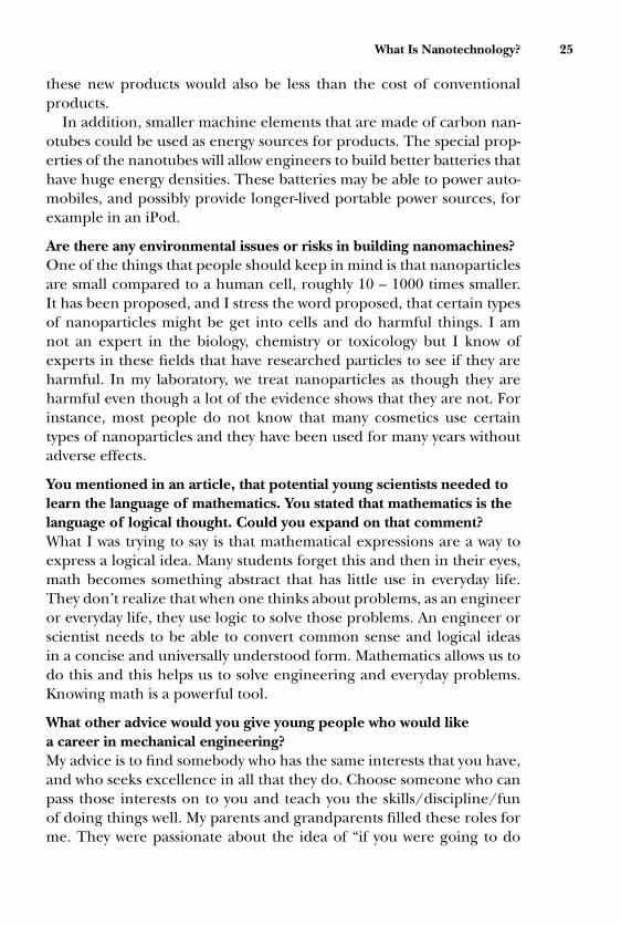
P1: 000
GGBD159C01 GR3880/Mongillo Top Margin: 5/8in Gutter Margin: 3/4in September 25, 2007 16:2
What Is Nanotechnology? 25
these new products would also be less than the cost of conventionalproducts.
In addition, smaller machine elements that are made of carbon nan-otubes could be used as energy sources for products. The special prop-erties of the nanotubes will allow engineers to build better batteries thathave huge energy densities. These batteries may be able to power auto-mobiles, and possibly provide longer-lived portable power sources, forexample in an iPod.
Are there any environmental issues or risks in building nanomachines?One of the things that people should keep in mind is that nanoparticlesare small compared to a human cell, roughly 10 – 1000 times smaller.It has been proposed, and I stress the word proposed, that certain typesof nanoparticles might be get into cells and do harmful things. I amnot an expert in the biology, chemistry or toxicology but I know ofexperts in these fields that have researched particles to see if they areharmful. In my laboratory, we treat nanoparticles as though they areharmful even though a lot of the evidence shows that they are not. Forinstance, most people do not know that many cosmetics use certaintypes of nanoparticles and they have been used for many years withoutadverse effects.
You mentioned in an article, that potential young scientists needed tolearn the language of mathematics. You stated that mathematics is thelanguage of logical thought. Could you expand on that comment?What I was trying to say is that mathematical expressions are a way toexpress a logical idea. Many students forget this and then in their eyes,math becomes something abstract that has little use in everyday life.They don’t realize that when one thinks about problems, as an engineeror everyday life, they use logic to solve those problems. An engineer orscientist needs to be able to convert common sense and logical ideasin a concise and universally understood form. Mathematics allows us todo this and this helps us to solve engineering and everyday problems.Knowing math is a powerful tool.
What other advice would you give young people who would likea career in mechanical engineering?My advice is to find somebody who has the same interests that you have,and who seeks excellence in all that they do. Choose someone who canpass those interests on to you and teach you the skills/discipline/funof doing things well. My parents and grandparents filled these roles forme. They were passionate about the idea of “if you were going to do

P1: 000
GGBD159C01 GR3880/Mongillo Top Margin: 5/8in Gutter Margin: 3/4in September 25, 2007 16:2
26 Nanotechnology 101
something, then do it right.” My grandfathers had a passion for workingon mechanical things and those skills they had were like magic to me.I wanted to learn to do what they could do. They also did an excellentjob and by observing their habit of excellence, I came to expect a lotfrom myself whenever I do something. Young people should also finda mentor that can pass on to them an understanding of why things areimportant and why they are relevant to everyday life. At the same time,make sure you have fun doing what interests you. For instance, if you lovemusic or acting, you can learn mechanical engineering and/or physicsand then apply them to make better instruments or devices for sets. Thesame thing applies to people that love cars, robots, airplanes, medicine,woodworking, and sports. You can use mechanical engineering, math,and physics to make useful contributions in these areas and have greatfun at the same time.
Would you want any of our readers (teachers/students) to contact youat your lab or by e-mail?My lab’s Web site is http://pcsl.mit.edu
E-mail ([email protected]) is OK, but I can’t guarantee a responsedue to the fact that I receive about 100–200 non-spam e-mails per daythat I have to respond to.
NANO ACTIVITY: CUTTING IT DOWN TO NANO
The activity, “Cutting It Down to Nano,” is adapted from the educationteam at MRSEC (Materials Research Science and Engineering Center)at the University of Wisconsin.
The challenge of the activity is to determine the number of timesyou need to cut the strip of paper in half in order to make itbetween 0 and 10 nanometers long. See the following Web sitefor more information about the activity: mrsec.wisc.edu/Edetc/IPSE/educators/activities/supplements/cuttingNano-Handout.pdf.
� For more activities to do from MRSEC, go to Web site: http://mrsec.wisc.edu/Edetc/IPSE/educators/cuttingNano.html
READING MATERIAL
Brezina, Corona. Careers in Nanotechnology. New York: Rosen Publishing Group, 2007.Fritz, Sandy. Understanding Nanotechnology: From the Editors of Scientific American. New
York: Warner Books, 2002.Johnson, Rebecca, L. Nanotechnology (Cool Science). Minneapolis, MN: Lerner Publi-
cations, 2005.

P1: 000
GGBD159C01 GR3880/Mongillo Top Margin: 5/8in Gutter Margin: 3/4in September 25, 2007 16:2
What Is Nanotechnology? 27
Poole, Charles P., and Frank J. Owens. Introduction to Nanotechnology. Hoboken, NJ:John Wiley & Sons, Wiley-Interscience, 2003.
Ratner, Mark, and Daniel Ratner. Nanotechnology: A Gentle Introduction to the Next BigIdea. Upper Saddle River, NJ: Prentice Hall, 2003.
Shelley, Toby. Nanotechnology: New Promises, New Dangers (Global Issues). London: ZedBooks, 2006.
VIDEOS
What Is Nanotechnology? An engineer from University of Wisconsin-Madison,Wendy Crone is on a mission. She and her interns are creating user-friendly exhibitsto teach the public about the nanoworld. http://www.sciencedaily.com/videos/2006-06-11/
Work Force Preparation. Are We Prepared to Get into the Nanotechnology Work-force? Professor Wendy Crone. Conversations in Science. Madison MetropolitanSchool District. UW-Madison Interdisciplinary Education Group. http://mrsec.wisc.edu/Edetc/cineplex/MMSD/prepared.html
When Things Get Small. Google Video. Describes how small is a nanometer? Thefilm shows how scientists layer atoms to form nanodots. http://video.google.com/videoplay?docid=-215729295613330853
Careers in Nanotechnology Information Video. Penn State University. http://www.cneu.psu.edu/nePublications.html
WEB SITES
The Foresight Institute: Nonprofit institute focused on nanotechnology, the comingability to build materials and products with atomic precision, and systems to aidknowledge exchange and critical discussion, thus improving public and privatepolicy decisions. http://www.foresight.org/
National Nanotechnology Initiative: The National Nanotechnology Initiative (NNI)is a federal R&D program established to coordinate the multiagency efforts innanoscale science, engineering, and technology. http://www.nano.gov/
Scientific American: Nanotechnology articles, some free and some archived,http://www.sciam.com/nanotech/
SOMETHING TO DO
Make a nanoruler to measure objects at the nanoscale. Go to the Lawrence Hall ofScience site for the instructions, http://www.nanozone.org/nanoruler print.htm

P1: 000
GGBD159C01 GR3880/Mongillo Top Margin: 5/8in Gutter Margin: 3/4in September 25, 2007 16:2
P1: 000
GGBD159C02 GR3880/Mongillo Top Margin: 5/8in Gutter Margin: 3/4in September 25, 2007 16:2
2
The Science ofNanotechnology
Nanotechnology is having the ability and the knowledge to manufactureproducts at the nanoscale—one billionth of a meter. All materials thatare one-billionth of a meter are invisible to the human eye. The nakedeye can see to about 20 microns. A micron (10−6) is one-millionth of ameter. Even using an optical microscope that uses light energy, we canonly see materials that are about 1 micron in size.
In Chapter 1 you read about a number of nanotechnology prod-ucts that are sold today. These products included pants that are stain-resistant, sunscreens that protect the skin against sun rays, medical dress-ings that are used for burn victims and special nanoparticles used tomake tennis rackets and hockey sticks. So, how can you “see,” manipu-late, and make products at the nanometer scale, the size of atoms andmolecules?
To understand how nanotechnology can be used to manufacture thesenanoproducts, you need to review the science of:
� matter and its forms,� matter’s smallest particles—atoms and molecules,� chemical bonding of atoms and molecules,� molecular self-assembly, and� how to manipulate matter at a scale of 1 to 100 nanometers.
WHAT IS MATTER?
Forms of Matter
Look around you. Everything around you is made up of matter. Matteris the air you breathe, the water you drink, the food you eat, the clothesyou wear, and the home you live in.

P1: 000
GGBD159C02 GR3880/Mongillo Top Margin: 5/8in Gutter Margin: 3/4in September 25, 2007 16:2
30 Nanotechnology 101
Table 2.1 International System of Measurement [Systeme Internationald’Unites (SI Units)]
Unit Abbreviation DescriptionScientificNotation
meter m approximately 3 feet 1 mcentimeter cm 1/100 of a meter, about
1/2 inch10−2
millimeter mm 1/1000 of a meter 10−3
micrometer µm 1/1,000,000 of a meter, oftencalled a micron
10−6
nanometer nm 1/1,000,000,000, the size of asingle molecule
10−9
Matter is anything that has mass and volume. Mass is the amount ofmatter in an object and volume is the amount of space occupied by anobject. Matter exists in three principal forms, called phases—gas, liquid,and solid.
Gas, or vapor, is the most energetic phase of matter. In gases, theparticles (individual atoms or molecules) are far apart from each otherand can move about freely. Air neither holds its shape nor its volumebecause particles move freely through open space. As a result, gasesexpand to fill the shape of their container. A gas, such as oxygen, isin constant motion and takes the shape of and completely fills anycontainer holding it.
In liquids, the particles are much closer together. So liquids are farmore difficult to compress. The particles that make up liquids moveabout, enabling liquids to change shape easily. A liquid takes the shapeof the container holding it.
In solids, the forces between the particles are strong enough to holdthe particles together in specific positions causing solids to maintain
� What is Matter?. If you have time, you maywant to watch the video, Go to: http://www.wpsu.org/nano/lessonplan detail.php?lpid=21
their shape. As an exam-ple, copper holds it shapebecause the particles staybound together in a regularpattern.
Properties of Matter
The different forms of matter have physical properties and chemi-cal properties that are characteristic of individual substances. Physical

P1: 000
GGBD159C02 GR3880/Mongillo Top Margin: 5/8in Gutter Margin: 3/4in September 25, 2007 16:2
The Science of Nanotechnology 31
properties of a substance include color, odor, hardness, density, and theability to conduct electricity and heat. We distinguish different types ofmatter by the differences in such physical properties. As an example,the formation of ice is a physical phase change, freezing of water. Eachsubstance has unique phase change properties, such as the tempera-tures, at which freezing or boiling of the substance occurs, known as the“freezing point” and “boiling point.”
Chemical properties describe the ability of a substance to change fromone kind of substance into a new and different brand-new substance.The formation of iron oxide (rust) is a chemical change. The moreproperties you can identify in a gas, liquid, or solid, the better you knowthe nature of that substance.
PROPERTIES OF MATTER CHANGE AT THE NANOSCALE
The properties of matter depend in part on size. The physical, chemi-cal, and biological properties of matter generally differ at the nanoscalewhen compared to the larger quantities of the same material. This isdue, in part, to the difference in surface area per unit of volume at thenanoscale.
Suppose we have a cube of salt. Its volume area is length times heighttimes depth. Let’s say that the block is 1 mm × 1 mm × 1 mm, whichis 1 cubic millimeter altogether. (We’re using millimeters (mm) insteadof nanometers for simplicity.)
The cube has 6 square sides, each of which is (1 mm × 1 mm) 1 squaremm in area, so the whole cube has an area of 6 square mm. The ratio ofthe area (A) of the cube to the volume (V) of the cube is A divided byV (written “A/V”) or a ratio of 6/1. Now, in contrast, suppose we havea bigger cube of salt whose edges are 2 mm long instead of 1 mm, sothis cube has a volume (2 × 2 × 2) of 8 cubic mm. The area of eachside of this salt cube is 2 mm × 2 mm, or 4 square mm, and the areaof the cube’s entire surface then is 6 × 4 square mm, or 24 square mm.So the area-to-volume ratio of the big block is 24 divided by 8, whichequals an A/V ratio of 3/1. So, the bigger cube has a smaller A/V ratiothan the smaller cube. This example demonstrates how smaller cubeswill have greater ratios of surface area to volume. Table 2.2 summarizesthis principle.
This table illustrates how as the sides of a cube get shorter, the volumeof a cube gets smaller more quickly than its surface area, so the ratioA/V increases. The ratio A/V is twice as great for the cube of 1 mm asfor the cube of 2 mm, and three times as great as the cube of 3 mm. Thisphenomenon happens on the nanoscale very significantly.

P1: 000
GGBD159C02 GR3880/Mongillo Top Margin: 5/8in Gutter Margin: 3/4in September 25, 2007 16:2
32 Nanotechnology 101
Table 2.2 Surface Area Per Unit of Volume
Length of Side ofCube
Volume of Cube(V)
Surface Area ofCube (A) Ratio of A/V
3 mm 27 54 22 mm 8 24 31 mm 1 6 6
Notice how the ratio of area to volume changes as the cube becomes smaller.
For a given substance, increasing the number of nanoscale particlesalso increases the proportion of atoms on the surface compared with thenumber of internal atoms. Atoms at the surface often behave differentlyfrom those located in the interior. Atoms at the surface have a higherenergy state, which means they are more likely to react with particlesof neighboring substances. The result is that chemical reactions cantake place between atoms and molecules at surfaces acting as miniaturechemical reactors.
By modifying materials at the nanoscale other properties such asmagnetism, hardness, and electrical and heat conductivity can bechanged substantially. These changes arise from confining electronsin nanometer-sized structures. As one example, electrons (subatomicparticles) do not flow in streams as they do in ordinary electrical wires.At the nanoscale, electrons act like waves. When electrons act as waves,they can pass through insulation that blocks flowing electrons.
Another example of changes at the nanoscale is that some nano sub-stances that should not dissolve in a liquid actually do dissolve. Someelements like gold also show change at the nanoscale. At the macro scale,gold metal is shiny yellow as you noticed in jewelry. If you break up thegold, to particle 100 nanometers wide, it still looks shiny yellow. But,when you break down the particle of gold to 30 nanometers across, thegold appears bright red. As the particle of gold gets even smaller than30 nanometers, it looks purple and when it is a little bit smaller it willappear brownish in color. Color can change in some other substances,like gold, at the nanoscale. Physical properties including strength, crys-tal shape, solubility, thermal and electrical conductivity, and magneticand electronic properties also change as the size decreases.
Let’s look at another example of how a physical property changesat the nanometer scale. At the macro scale, a sheet of aluminum isharmless. However, when the particles of aluminum are cut down in sizeto 20 to 30 nanometers, the metal can explode.

P1: 000
GGBD159C02 GR3880/Mongillo Top Margin: 5/8in Gutter Margin: 3/4in September 25, 2007 16:2
The Science of Nanotechnology 33
Volume to Surface Area
Nanomaterials have a large proportion of surface atoms, and the sur-face of any material is where reactions happen. Because of nanoparticles’
Did you know?Quantum mechanics is the study of matter and ra-diation at the atomic level.
huge surface area and thusvery high surface activity,nanotechnologists can po-tentially use much less mate-rial. The amount of surfacearea also allows a fast reaction with less time. Therefore, many pro-perties can be altered at the nanoscale. That’s the power of nanotech-nology.
MATTER’S SMALLEST PARTICLES: MATTER IS MADE UPOF ELEMENTS
Nanotechnology’s raw materials are the chemical elements. Any sam-ple of matter, whether it is a gas, liquid, or solid, is either an elementor is composed of several elements. Elements are known as the buildingblocks of matter. An element consists purely of atoms of one kind. It isa substance composed of pure chemicals that cannot be separated intosimpler substances. Therefore, an element is always an element, even atthe nanoscale.
Sulfur, copper, carbon, oxygen, iron are some common examplesof pure chemical elements. Just four of these—carbon (C), oxy-gen (O), hydrogen (H), and nitrogen (N)—make up approximately96 percent of the human body. Much of Earth, including the uni-verse, consists of several elements, such as carbon, hydrogen, oxy-gen, and nitrogen that are found in our bodies, too. Other com-mon elements include iron, copper, calcium, nickel, potassium, andmercury. Many of these elements are listed on the side of vitaminbottles.
The Periodic Table of Elements
The chemical elements are arranged in a chart called the PeriodicTable of Elements. The table of elements represents the building blocksof everything—both living and nonliving. About 90 elements have beenidentified as occurring naturally on Earth. The Periodic Table of Ele-ments is an important tool for scientists.
The table helps them understand the physical and chemical proper-ties of individual elements.

P1: 000
GGBD159C02 GR3880/Mongillo Top Margin: 5/8in Gutter Margin: 3/4in September 25, 2007 16:2
34 Nanotechnology 101
Table 2.3 The Major Elements Found in the Human Body
Element Symbol Approximate Percent by Mass in Human Body
Oxygen O 65,0Carbon C 18.5Hydrogen H 9.5Nitrogen N 3.3Calcium C 1.5Phosphorus P 1.0Potassium K 0.4Sulfur S 0.3Sodium Na 0.2Chlorine Cl 0.2Magnesium Mg 0.1
The Periodic Table can be divided into three basic groups of elements.The groups include metals, nonmetals, and semimetals or metalloids.Semi-metals have the properties of both metals and nonmetals. Chemistsuse one or two letter symbols to represent elements. As an example, thesymbol for aluminum is Al. The symbol for oxygen is O.
� The metal elements make up the majority of the groups of elements—more than 70 percent. Some of these metals include potassium, calcium,sodium, barium, and the more familiar ones include such metals as tin,lead, aluminum, copper, mercury, silver, and gold. Mercury is the onlymetallic element that is liquid at room temperature. Gold and silvernanoparticles are used in medical research and for treating burns andwounds and in cancer research. Most metals are good conductors of elec-tricity and heat and are malleable—easy to bend and shape. However,electrical conductivity in metal decreases with increasing temperature,whereas in semiconductors, electrical conductivity increases with increas-ing temperature.
� Some of the nonmetals include chlorine, bromine, iodine, and fluorine.The nonmetals are dull in color, usually brittle, and are poor conductors ofelectricity and heat. You are not going to find too many of these elementsin nanofabrication.
� A few elements are classified as metalloids or semimetals because theyare between a metal and a nonmetal. The metalloids include silicon (S),boron (B), germanium (Ge), arsenic (As), and tin (Sn). Metalloids haveproperties of both metals and nonmetals.

P1: 000
GGBD159C02 GR3880/Mongillo Top Margin: 5/8in Gutter Margin: 3/4in September 25, 2007 16:2
The Science of Nanotechnology 35
Some of the metalloids, such as silicon and germanium, are used assemiconductors in transistors. Transistors are the fundamental buildingblocks of a microchip and are built on a silicon base.
Semiconductors
A semiconductor is a common term used in the electronics and thecomputer field. Semiconductors are generally made from certain ele-ments such as silicon, germanium, and chemical compounds such aslead sulfide.
Semiconductors have a special atomic structure that allows their con-ductivity properties (both good and not so good) to be controlled by en-ergy from electric currents, electromagnetic fields, or even light sources.As an example, when you apply heat energy to a semiconductor you canincrease its conductivity of electricity. These semiconductor propertiesmake it possible to use them to make products such as transistors, inte-grated circuits, and many other types of electronic devices.
These 10 elements make up most of the matter in the universe.
Element 1: Hydrogen
Element 2: Helium
Element 3: Lithium
Element 4: Beryllium
Element 5: Boron
Element 6: Carbon
Element 7: Nitrogen
Element 8: Oxygen
Element 9: Fluorine
Element 10: Neon
SMALLEST PART OF AN ELEMENT: THE ATOM
The smallest quantity of an element, which has all of the propertiesof the element, is an atom. An atom is a microscopic structure found inall ordinary matter around us.
Atoms are extremely small, on the order of one to several nanometerswide. A nanoparticle would be a collection of tens to thousands of atomsmeasuring about 1 to 100 nanometers in diameter. As an example, itwould take more than a million atoms to match the thickness of thisbook page.

P1: 000
GGBD159C02 GR3880/Mongillo Top Margin: 5/8in Gutter Margin: 3/4in September 25, 2007 16:2
36 Nanotechnology 101
SsWriting with Atoms
In 1989, scientists at the IBM Research Center in San Jose, California, con-ducted an interesting activity using atoms. The scientists manipulated 35
Did you know?Xenon (Xe) is a gas most widely used in light-emitting devices called Xenon flash lamps, whichare used in photographic flashes, stroboscopiclamps, to excite the active medium in lasers whichthen generate coherent light, in bactericidal lamps(rarely), and in certain dermatological uses.
atoms of the gas xenon (Xe),to write the letters, IBM. IBMis the name of their company.The letters were 500,000 timessmaller than the type size ofletters used in printing thisbook. To place the atoms inthe form of the three letters,the scientists used a special tip
on scanning tunneling microscope (STM) to push the atoms into place. Thebumps you see in the photo (p. 37) are individual atoms. They have beenmoved precisely into position, in a row, one half nanometer from eachother.
Ss
See Chapter 3 for more information about nanotechnology micro-scopes.
INSIDE THE ATOM: SUBATOMIC PARTICLES
The three basic kinds of subparticles that make up the atom consistof neutrons, protons, and electrons.
Neutrons and Protons
Almost all the mass of an atom is in the nucleus. The nucleus lies at thecenter of the atom. The nucleus consists of two types of particles, protonsand neutrons. These two particles are called nucleons, the buildingblocks of the atomic nuclei.
The protons have a positive electric charge. Neutrons do not haveany electric charge; therefore they are an electrically neutral subatomicparticles of the nucleus. The strong nuclear force binds protons andneutrons together to make the nucleus.
Electrons
Electrons exist outside the nucleus. Electrons carry a negative charge,equal in magnitude and opposite to the charge of a proton. An electronis 1/1836 the mass of a proton and is much smaller. Electrons carry elec-trical current and the manipulation of these electrons allows electronic
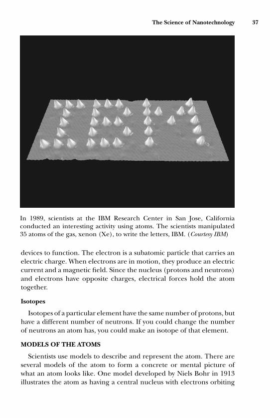
P1: 000
GGBD159C02 GR3880/Mongillo Top Margin: 5/8in Gutter Margin: 3/4in September 25, 2007 16:2
The Science of Nanotechnology 37
In 1989, scientists at the IBM Research Center in San Jose, Californiaconducted an interesting activity using atoms. The scientists manipulated35 atoms of the gas, xenon (Xe), to write the letters, IBM. (Courtesy IBM)
devices to function. The electron is a subatomic particle that carries anelectric charge. When electrons are in motion, they produce an electriccurrent and a magnetic field. Since the nucleus (protons and neutrons)and electrons have opposite charges, electrical forces hold the atomtogether.
Isotopes
Isotopes of a particular element have the same number of protons, buthave a different number of neutrons. If you could change the numberof neutrons an atom has, you could make an isotope of that element.
MODELS OF THE ATOMS
Scientists use models to describe and represent the atom. There areseveral models of the atom to form a concrete or mental picture ofwhat an atom looks like. One model developed by Niels Bohr in 1913illustrates the atom as having a central nucleus with electrons orbiting

P1: 000
GGBD159C02 GR3880/Mongillo Top Margin: 5/8in Gutter Margin: 3/4in September 25, 2007 16:2
38 Nanotechnology 101
Figure 2.1 Atom diagram. (Courtesy of Jeff Dixon)
around it. In the 1920s scientists improved on the model of the atom.One theory is that the electrons move about in a cloud-like regionsurrounding the nucleus. The electron cloud represents some probablelocations of where the electrons are likely to be at a set time.
These models should not be interpreted as any visual representationof an atomic model or as a recreation of an actual atom. The best modelsare those that are purely mathematical. However, the atomic modelimages do help as a guide in understanding concepts in chemistry andother sciences.
Early Atomic Theory by Empedocles and Democritus
Empedocles was a Greek philosopher and scientist who lived in Sicilybetween 492 B.C. and 432 B.C. One of his theories was to describe thingsaround us. Empedocles proposed that all matter was composed of fourelements: fire, air, water, and Earth. As an example, stone was believed tocontain a higher amount of Earth than the other elements. The rabbitwas believed to contain a higher amount of both water and fire than theother two elements.

P1: 000
GGBD159C02 GR3880/Mongillo Top Margin: 5/8in Gutter Margin: 3/4in September 25, 2007 16:2
The Science of Nanotechnology 39
Another Greek philosopher, Democritus, who lived from 460 B.C.to 370 B.C., developed another theory of matter. He believed that allmatter was made of tiny parts. He demonstrated his idea by stating ifsomeone continued to cut an object into smaller and smaller pieces, youwould reach the point where the piece was so tiny that it could no longerbe cut up and divided. Democritus called these small pieces of matteratomos, meaning “indivisible.” He suggested that atomos, or atoms, wereeternal and could not be destroyed. During his time, Democritus didnot have the means that could prove or disprove his theory or eventest it.
Atomic Number and Atomic Mass
The number of protons in the nucleus of an atom determines anelement’s atomic number. In other words, each element has a uniquenumber that identifies how many protons are in one atom of that el-ement. For example, all hydrogen atoms, and only hydrogen atoms,contain one proton and have an atomic number of 1. All carbon atoms,and only carbon atoms, contain six protons and have an atomic numberof 6. Oxygen atoms contain 8 protons and have an atomic number of 8.The atomic number of an element never changes.
Atomic masses of elements, however, depend on the number of neu-trons as well as protons in an atom and differ from their atomic numbers.Atomic mass is indicated in the periodic table of elements as Atomic MassUnits (AMU) and is a larger value than the atomic number.
ATOMS AND MOLECULES
Nanotechnology is all about the manipulation of atoms andmolecules. Atoms seldom exist in a solitary state. Occasionally, atoms
� You may want to see the video, NanoMani-pulator: Seeing and Touching Molecules. http://www.nanotech-now.com/multimedia.htm
join together with their ownkind of element. Sometimes,the atom joins together withother elements. When anatom of one element chem-ically combines with an atom of another kind of element, they form acompound. For example, water (H20) is a compound made from twoelements, hydrogen (H) and oxygen (O). The smallest part of the com-pound is a molecule, a combination of two or more atoms.
Molecules range in size from a few atoms to thousands of atoms. Howdo atoms join together to form molecules?

P1: 000
GGBD159C02 GR3880/Mongillo Top Margin: 5/8in Gutter Margin: 3/4in September 25, 2007 16:2
40 Nanotechnology 101
MOLECULES AND CHEMICAL BONDING
Knowing how molecules bond together is important in understandinghow nanostructures can be manufactured.
Molecules are combinations of atoms held together by chemicalbonds. A chemical bond is actually an electrostatic force between elec-trons and protons and between atoms and molecules. One researcharticle stated the electrostatic force is quite strong. Electrostatic forcesare more than 1000 times as strong as gravitational forces. The chemicaland physical properties of matter result from the ability of atoms to formbonds from electrostatic forces. There are two main types of chemicalbonds that hold those atoms together. They are called ionic bonds andcovalent bonds.
Ionic Bonding
Atoms can lose or gain electrons forming an ion, which has a netelectric charge. A negative charged ion, called an anion (pronounced/AN-ion/), is formed when an atom or a special group of atoms gainsadditional electrons. When an atom loses some electrons, a positivecharged ion is created called a cation (pronounced CAT-ion).
Ionic bonding takes place between two oppositely charged ions, ananion and a cation. Ions may consist of a single atom or multiple atoms,in which a group of atoms is called a “polyatomic ion.” Examples ofpolyatomic anions include: carbonate ion, which is composed of carbonand oxygen; and sulfate ion, which is composed of sulfur and oxygen.An example of a polyatomic cation is ammonium ion, which consists ofnitrogen and hydrogen. Cations are usually metal atoms and anions areeither nonmetals or polyatomic ions (ions with more than one atom).The attraction of the two charges holds the atoms or molecules together.Electrostatic forces hold ionic bonds together. Many compounds madeup of an anion and cation will dissolve in water, so that the two ionsseparate in the water and make an ionic solution. Ionic solutions areused for treating and cleaning the eye.
Ionic bonding occurs between an element that is a metal and one thatis a nonmetal. The majority of geological materials, such as minerals androcks, feature ionic bonding, predominantly.
Covalent Bonds and Monomers
Covalent chemical bonds are different from ionic bonding. Covalentbonding involves the sharing of a pair of electrons by two atoms. A

P1: 000
GGBD159C02 GR3880/Mongillo Top Margin: 5/8in Gutter Margin: 3/4in September 25, 2007 16:2
The Science of Nanotechnology 41
molecule of water, written H20, is held together by covalent bonds. Thetwo elements, hydrogen and oxygen, share electrons.
Covalent bonding occurs between two elements that are nonmetals.Much of the matter of substances in your everyday life, the solids, liquids,and gases, are the results of covalent bonding. Covalent bonds occurin all sorts of organic substances, including materials associated withliving things, such as plant or animal tissue, food, and the like. Covalentbonding predominates in biological systems, although ions have veryimportant roles in these systems, too.
A Monomer
A small molecule that is held together by covalent bonding is calleda monomer (from Greek mono “one” and meros “part”). Examples ofmonomers are hydrocarbons that consist only of the elements carbon(C) and hydrogen (H). Hydrocarbons are combustible when they com-bine with oxygen. They are the main components of fossil fuels, whichinclude petroleum, coal, and natural gas. When the covalent bonds ofthese types of substances are broken they will release energy, which iswhat occurs when fossil fuels burn.
From Monomers to Polymers
Monomers may become chemically bonded to several other similarmonomers to form a polymer. A polymer is a term used to describe avery long molecule consisting of structural units and repeating unitsconnected by covalent chemical bonds. When monomers are linkedtogether to each other during a chemical reaction, it is called poly-merization. Often polymerization occurs as a chain reaction, which willcontinue until a large number of the monomers have combined (poly-merized) with each other. The result of polymerization is a chain orother network of linked monomers that can be formed into fibers,sheets, fabrics, foams, or other structures, depending on the type ofpolymer.
Polymers can occur naturally, mainly in living organisms, or synthet-ically, through manufacturing. A few general examples of naturally oc-curring polymers include proteins, starches, and cellulose. Starches arepolymers composed of sugars. Latex, from the sap of rubber trees, canbe made to polymerize into latex rubber. The genetic materials DNA andRNA found in chromosomes and cells are also types of polymers. Severalnatural fibers such as wool, silk, and spider web thread are polymers.Scientists and engineers study the formation, structure, and propertiesof such natural polymers as models for synthetic nanomaterials.

P1: 000
GGBD159C02 GR3880/Mongillo Top Margin: 5/8in Gutter Margin: 3/4in September 25, 2007 16:2
42 Nanotechnology 101
Figure 2.2 Polymer. (Courtesy of Jeff Dixon)
Polymers and Nanotechnology
Polymerization is commonly used for making nanoscale materialsand other materials as well. Polymerization is used to create the plastic
Did you know?DNA is another example of a polymer.
materials found in thou-sands of strong, flexible, andlightweight products in youreveryday life. Some familiarexamples of polymers include the common plastics, polystyrene, andpolyethylene. These kinds of polymers are used in everything fromfood containers and packaging materials to cars, boats, and comput-ers. Polyvinyl alcohol is a main ingredient in latex paints, hair sprays,shampoos, and glues, and waxes and oils. Let’s look at some examplesof applications of polymerization in nanotechnology.
Polymer-Based Nanosponges
At the Los Alamos National Laboratory in Los Alamos, New Mexico,scientists have developed a reusable polymer-based nanosponge. Thenanosponge has nanometer-sized pores that can absorb and trap or-ganic contaminants in water. The Nanosponge polymer can be usedto clean up organic explosives and oil or organic chemical spills espe-cially in water, while decreasing clean up costs associated with presenttechnologies. The nanosponge is made up of polymeric building blocksthat form cylindrical cages to trap organics. After the sponges are satu-rated with contaminants, they can be rinsed with ethanol to remove thecontaminants and the nanosponge can then be reused.
The polymer sponge has multiple applications. For example, a poly-mer designed as a membrane can be placed on a water faucet. Themembrane can be used to treat and purify the water for drinking andcooking uses. One advantage of using polymers is that they are inex-pensive to manufacture and can be used in a variety of water treatmentsystems.

P1: 000
GGBD159C02 GR3880/Mongillo Top Margin: 5/8in Gutter Margin: 3/4in September 25, 2007 16:2
The Science of Nanotechnology 43
Polymer Solar Cells
In the hope of making solar energy more useful and affordable, sev-eral scientists have been working on creating organic photovoltaic cells.Their goal is to replace the usual silicon (S) with readily available ma-terials such as carbon (C). If they succeed, designers could one dayintegrate solar cells into everyday gadgets like iPods and cell phones.Even the energy absorbed by window tinting could be used to power alaptop, for example.
One team of researchers at the University of California have devel-oped an organic photovoltaic cell that uses a polymer, or plastic, materialin a unique way. Like other organic solar cells, the plastic material intheir prototype includes a polymer material. The material, composed ofcommon chemicals, is sandwiched between conductive electrodes. Pho-tons in the sunlight “knock” electrons from the polymer onto one ofthe electrodes. This causes an electrical imbalance where one electrodebecomes positively charged while the other is negatively charged. Whenthis happens an electrical current is created. See Chapter 8 for moreinformation about solar cells.
A Unique Class of Synthetic Polymers, Dendrimers
One unique class of polymers is dendrimers. Dendrimers play animportant role in nanotechnology. Dendrimers, which are synthesized
Did you know?Dendrimer comes from the Greek word dendra,meaning tree. The term dendritic describes any-thing that has a branched, tree-like structure.
from monomers, are tree-like highly branched poly-mer molecules that areabout 3 nanometers across.
Several different kinds ofdendrimers have been syn-thesized. They can be very useful in low-cost plastics such as radiatorhoses, weather stripping, and gasket seals. In biotechnology applica-tions, dendrimers are useful for their antiviral properties.
Dendrimers and Drug Delivery
Nanotechnology has the potential to be very useful for improving drugdelivery in treating patients with illnesses and diseases. The delivery ofdrugs into the body cannot be a hit or miss effort. The drug moleculeshave to find the exact place in the body where they can be the mosteffective. An anticancer drug needs to be delivered to a tumor where itcan do the most good. You do not want the anticancer drug deliveredto another organ in the body.

P1: 000
GGBD159C02 GR3880/Mongillo Top Margin: 5/8in Gutter Margin: 3/4in September 25, 2007 16:2
44 Nanotechnology 101
Dendrimers have several advantages in drug delivery; Dendrimerscan hold a drug’s molecules in their structure and deliver the drug toa particular part of the body such as a tumor. Dendrimers can entercells easily and release drugs on target and don’t trigger immune systemresponses.
Dendrimers can also be used for chemical analysis and diagnosis ofthe human body and to locate, diagnose, and then treat tumors or othersick cells. However, more research in safety issues needs to be done.
Dendrimers are of particular interest for cancer applications. Oneimportant factor is that it is easy to attach a large variety of other
Did you know?The term dendrimer was first used and patented byDonald Tomalia and others and Dow Chemical inthe 1980s.
molecules to the surface ofa dendrimer. These mole-cules could include tumor-targeting agents that canpinpoint tumors, deliver ananticancer drug to a tumor,
and may detect if the cancer drug is working.
MOLECULAR SELF-ASSEMBLY AND NANOFABRICATION
The term used for the manufacturing of nanoproducts and nanostruc-tures is nanofabrication. One branch of nanofabrication is self-assembly.Self-assembly is a strategy in which objects and devices, such as atomsand molecules, can arrange themselves into an orderly structure or finalproduct without any outside assistance. Self-assembly could occur if youcould shake a box of separated puzzle pieces, then look inside the boxto see a finished puzzle. The puzzle pieces self-assembled. Materials thatself-assemble include snowflakes, salt crystals, and soap bubbles. Eachone arranges itself into a pattern.
In the human body, the self-assembly process is similar to the way yourbones grow. Individual molecules are formed layer by layer on a surfaceof the bone. Self-assembly occurs spontaneously when the human bodyconverts food, water, and air into a variety of acids, sugars, and minerals.From these materials cells, blood, tissues, and muscles are created. Allof these biological functions are due to the self-assembly of moleculesin the human body which continue to build and repair cells and storeenergy all day long.
What is the advantage of using self-assembling in nanofabrication?One major reason is that to design and assemble nanoparticles atom byatom to make a lot of products is too slow and costly. Also, the atomsare too small for anyone to direct, find, and place individually andquickly.

P1: 000
GGBD159C02 GR3880/Mongillo Top Margin: 5/8in Gutter Margin: 3/4in September 25, 2007 16:2
The Science of Nanotechnology 45
Self-Assembly. Many researchers are exploring self-assembly of molecules atthe nanoscale to produce structures. In this activity, middle school studentsare modeling how self-assembly takes place. In this activity several LEGO R©
blocks are placed peg-side down on water. In time, the bricks will interactwith the surface tension of the water and with each other to assemble intoa pattern. (Courtesy Dean Campbell)
SOAP BUBBLES SELF-ASSEMBLE
Soap molecules can self-assemble into bubbles when you blow airthrough a soapy loop. The soap bubble molecules form two layers thatcontain a layer of water in between. The soap forms a monolayer onthe inside and a monolayer on the outside of the water. Each layer ofsoap is a self-assembled monolayer. The distance between the outer andinner layers of the bubble is about 150 nanometers. But the soap layercan become a bubble only when the conditions are just right. You needmostly air and very little water.
USING THE SELF-ASSEMBLY STRATEGY TO MAKE PRODUCTS
About one-quarter of the 2,000 or so nanotechnology projects the Na-tional Science Foundation now sponsors involve molecular self-assembly.

P1: 000
GGBD159C02 GR3880/Mongillo Top Margin: 5/8in Gutter Margin: 3/4in September 25, 2007 16:2
46 Nanotechnology 101
Molecular self-assembly is the most important of the nanoscale fabrica-tion techniques because it’s fast, inexpensive, and produces less waste.
Some of the major companies investing heavily in self-assembly in-clude Merck, Pfizer, 3M, IBM, and Hewlett-Packard. About one-quarterof the 2,000 or so nanotechnology projects the National Science Foun-dation now sponsors involve self-assembly.
Many soft or fluid consumer products such as foods, paints, deter-gents, personal care products, and cosmetics contain nanometer struc-tures that are formed by the self-assembly of molecules.
OTHER APPLICATIONS OF MOLECULAR SELF-ASSEMBLY
Self-Assembly in Medicine
Using the self-assembly process in medicine applications could greatlyimprove orthopedic implants. The average life of an implant today isabout 15 years, according to the American Academy of OrthopedicSurgeons. When implants fail in the body, they often break or crack thebone they are attached to. It is also very difficult to get bone to grow onthe implant, which is usually made of titanium or ceramics.
Researchers have developed a special coating comprising moleculesthat self-assemble into a structure similar to that of bone. The researchshows that when such a coating is applied to an implant, bone cells adaptto these structures and grow onto them.
In another research project, scientists have designed artificialmolecules that self-assemble to form structures that they think could beused to create a piece of artificial spinal cord. The artificial spinal cordcould help paralyzed patients regain some mobility. The self-assembledmolecule structures would act as a scaffold in which spinal-cord tissueor bone tissue could regenerate.
Self-assembly could change the nature of drug making too. A re-search group in Rochester, New York, is working on molecules that canself-assemble into drugs. The drugs would have the potential to sensecells with a disease and target them with treatments. The self-assembledmolecules bind to specific genes that cause certain genetic diseases andthis process blocks the genes from functioning. Of course, self-assemblyin drug making still has to be proven nontoxic to humans. Humanclinical trials are necessary. There is also the lengthy federal approvalprocess to go through. Plus, scientists have yet to learn how to designthe right molecules and figure out how to force them to assemble incertain ways.

P1: 000
GGBD159C02 GR3880/Mongillo Top Margin: 5/8in Gutter Margin: 3/4in September 25, 2007 16:2
The Science of Nanotechnology 47
NanoSonic, Inc.
Several companies use molecular self-assembly to make products. Oneof the companies, NanoSonic Inc., is located in Blacksburg, Virginia,The company’s team of researchers is headed by the president, Dr.Richard Claus, a professor at Virginia Tech. NanoSonic Inc. makes apatented material called Metal RubberTM using a molecular layeringprocess, known as electrostatic self-assembly.
Metal RubberTM looks like brown plastic wrap, and has some amazingproperties, including elasticity. “We can stretch it to about 200 to 300percent of its original length, and it relaxes back,” says Dr. Claus. “It’svery tough. We can expose it to chemicals. We can put it in jet fuel. Wecan hit it with acetone. We can boil it in water overnight, and it doesn’tmechanically or chemically degrade. We can heat it up to about . . . 700Fahrenheit. It won’t burn. We can drop it down to about . . . minus 167degrees Fahrenheit, and it maintains its properties.”
To make Metal RubberTM, the scientists at Nanosonic built it moleculeby molecule. The nanotechnology process that is used is called electro-static molecular self-assembly. “The Metal RubberTM virtually assemblesitself,” says Dr. Claus.
The scientists start with a plastic or glass substrate, or base, that theyhave given an electric charge, either positive or negative. Then theydip the substrate alternately into two water-based solutions. One so-lution contains ionic molecules that have been given a positive elec-trical charge (cations). The other solution contains ionic moleculesthat have a negative charge. If the substrate has a positive charge,it goes into the negative molecules first. The molecules cling tothe substrate, forming a layer only one molecule thick. After thenext dipping, into positive molecules, a second ultrathin layer forms.Making Metal RubberTM, Dr. Claus explains, is like “making a layercake.”
Dr. Claus says that with Metal RubberTM, nanotechnology has pro-duced a material with many potential uses. One of the most exciting isto make what he calls “morphing aircraft structures. These are aircraftthat dynamically change the shape of their wings and their control sur-faces during flight,” he explains. “Almost the way that a hawk might flyalong, see prey, and change its shape to dive down. For a plane, youneed a material that’s mechanically flexible. But you also need a mate-rial with a surface that’s controlled by sensors and electrical conductorsthat allow it to do that sensing and change shape accordingly.”

P1: 000
GGBD159C02 GR3880/Mongillo Top Margin: 5/8in Gutter Margin: 3/4in September 25, 2007 16:2
48 Nanotechnology 101
NANO INTERVIEW: DR. RICHARD CLAUS, PRESIDENTOF NANOSONIC
Dr. Richard Claus is president of NanoSonic, Inc., located inBlacksburg, Virginia. Dr. Claus responded to questions from studentsat the ForwardVIEW Academy in North Kingstown, Rhode Island.The students under the guidance of their chemistry teacher, Ms.Catherine Marcotte, were involved in doing many of the activities inthe NanoSonic Kit. The following are questions that they addressed toDr. Claus.
What made you (Dr. Claus) want to study nanotech?I was teaching engineering at Virginia Tech and one of the students inmy group started a small project in the lab. That was in the early 1990s,and I have been interested ever since.
What college did you go to?Johns Hopkins University in Baltimore.
What was your major?As an undergraduate, I majored in Arts and Sciences. As a graduatestudent, I majored in Engineering.
How did you get started in Nanotechnology?I was working on the faculty at Virginia Tech and doing work witha number of students in the area of optical fibers. We had a projectwith a company to put magnetic coatings onto a fiber, and the stu-dent mentioned above tried a “nanotechnology” process to apply thecoating.
When did you get your first idea about starting NanoSonic?Again, I was teaching at Virginia Tech, and another company came tous and asked us to do a project with them. The university could notapprove the legal terms and conditions of the contract proposed by thecompany, so we went off campus and started our own company to dothe work. Our objective was really just to support a graduate student andnot to start a company.
Who comes up with all the NanoSonic ideas?We all do. We currently have 62 people at NanoSonic, and they are a veryinteresting mix of individuals with very different technical backgroundsand experiences. Most of our ideas are due to the combination of sug-gestions from our chemists and engineers and production people. One

P1: 000
GGBD159C02 GR3880/Mongillo Top Margin: 5/8in Gutter Margin: 3/4in September 25, 2007 16:2
The Science of Nanotechnology 49
of our key laboratory staff people has a background and education inart, and we depend on her extensively for suggestions.
Does nanotechnology have any impact on your life?Directly, no. But there are lots of parts of my life that relate to nanotech-nology that seem more fun now, like why the sky is blue (really) and howI can prevent the inside of my car windows from fogging.
What is the best thing you have ever done involving nanotechnology?The best thing I have ever done has been hiring good people who knowa lot more about many different aspects of nanotechnology and practicalmanufacturing than I do. They are the ones who do all of the work.
Has studying this field changed the way you look at some things?Yes, as I mentioned earlier. One example is that nanoparticles are in anumber of normal household products, like suntan lotion. A few monthsago, a group of us went to the local drugstore and spent about an hourlooking at ingredients on the backs of suntan lotion products.
How did you start the company?When Virginia Tech did not want to pursue the project with the companyI mentioned above, we started the company the following afternoononline using a credit card. It took about 15 minutes.
Is your job fun?Yes, very much.
Can you cut Metal RubberTM?Yes, with a pair of scissors or a knife. It has the consistency of a mousepad.
Could you send a small sample of Metal RubberTM to our school?Let me see if the people down in the production area have anything wecan send.
Could you visit our school?I would be glad to if I am up your way.
What led to your making Metal RubberTM?Several of us went to a large international conference and heard a talkby a professor at a major research university. He said that no one wouldever make anything big and thick using self-assembly processing. Theperson next to me, Dr. Jennifer Lalli, turned to me and whispered, “Wecan do that!” Within a few weeks, Dr. Lalli and her group had made ourfirst Metal RubberTM materials.

P1: 000
GGBD159C02 GR3880/Mongillo Top Margin: 5/8in Gutter Margin: 3/4in September 25, 2007 16:2
50 Nanotechnology 101
Are you taking the measures to protect the environment from thepollution of the process (is there any?) of making Metal RubberTM
because it will stop a lot of problems in the future?Yes, we are. The byproducts of the production process are not significantpollutants, but we work closely with our town to properly handle andtreat all of the materials that we generate.
Where would you dispose of Metal RubberTM?In a landfill most probably. Again, it is pretty much like a mousepad.
Is it environmentally safe and biodegradable?Safe, yes. Biodegradable, no. It is something like milk jug containers—they are safe but will not degrade in a landfill for a long time.
Can you recycle it into something else?Yes, we can. I was on the phone about this in particular about an hourago.
How did you hear about nanotech?Meetings and conferences mostly, and technical journals. I was a profes-sor at Virginia Tech for about 30 years, so I did a lot of reading aboutscience and engineering. I still do.
NANO ACTIVITY: NANOTECHNOLOGY DEMONSTRATION KITFROM NANOSONIC
You can learn more about self-assembly by doing some of the ex-periments in a nanotechnology school kit produced by Dr. Claus andthe scientists at NanoSonic Inc. The Nanotechnology Demonstrationkit provides experiments that are designed for middle and high schoolscience classes. The kit contains all of the materials you need for 24students. Instructions, worksheets, teacher aids, and a resource CD areprovided.
The purpose of the Nanotechnology Demonstration Kit is to allowsecondary school students to learn about nanotechnology and nextgeneration materials by making and testing nanostructured materialsby themselves using a minimum of laboratory supplies and ordinary tapwater.
The kit is divided into five units that will introduce students to thefollowing concepts.
� Nanotechnology and nanostructured materials� Chemical bonding

P1: 000
GGBD159C02 GR3880/Mongillo Top Margin: 5/8in Gutter Margin: 3/4in September 25, 2007 16:2
The Science of Nanotechnology 51
� Electrostatics� Electrostatic self-assembly� Fabrication of their own nanostructured film
To learn more about the kit, contact NanoSonic, www.nanosonic.comMs. Catherine Marcotte, a science teacher and her high school classes,
had the opportunity to use the Nanotechnology Demonstration Kit ofactivities produced by Professor Richard Claus of NanoSonic, Inc, andthe manufacturer of Metal RubberTM. Her class interviewed Dr. RichardClaus and asked him questions about his work. I asked Ms. Marcotteto comment on her experiences as a science teacher and her thoughtsabout the world at the nanoscale. Here are her comments.
“I am currently in my eleventh year teaching varied science topics tosmall, mixed groups of secondary school students at an alternative pub-lic school program called ForwardVIEW Academy in North Kingstown,Rhode Island.
“Most often, each spring or summer, a science theme, such as energy,water, or science, society, and technology as in this year, seems to be inthe air that becomes the core of my plans for the coming school year.Other times, the course is chosen and serendipity works its magic. Basicchemistry was the focus that year and, coincidentally, nanotechnologyseemed to be on the cover of every magazine.
“Then, I had the pleasure to meet the author Mr. John Mongillo,who brought everything together with a lab kit for high school scienceinvolving nanotechnology by NanoSonic, Inc., which he wanted to co-teach with me in my classes. I was thrilled. It fit in perfectly and alsoprovided the perfect segue to this year’s technology theme.
“The kit gave students the opportunity to apply the concepts of nan-otechnology, such as self-assembly, in making a film on a glass slide onemolecule layer at a time! In the unit, students were reminded of atomicstructure and learned of electrostatics, and were also made aware of themany careers available in the growing field of nanotechnology.
“Later, through John, the students and I had a rewarding conversa-tion with the President of NanoSonic, Inc., Dr. Richard Claus, by writingquestions for Dr. Claus to which he kindly responded by email. Theentire experience brought the classes’ imaginations far beyond the con-fines of the classroom, from the uses for flexible Metal RubberTM to evena lovely house in the misty, morning hills of Blacksburg, Virginia, andthe thoughtful musings of a scientist and company president in answerto the question, “Why do you say your job is fun?”

P1: 000
GGBD159C02 GR3880/Mongillo Top Margin: 5/8in Gutter Margin: 3/4in September 25, 2007 16:2
52 Nanotechnology 101
“There is a comfort available in studying nature at its unimaginablysmall, and learning about the incredible advances in nanotechnology.The rewards are wonder and amazement at the depth of order andbeauty in the physical world. While we thinking humans are capable ofappreciating this, we are also capable of that which can seem the antithe-sis of order and beauty. Nature can seem more reliable. Learning moreabout our world on the nanoscale and realizing our own membershipin it can, I think, provide a sense of reassuring continuity.”
READING MATERIAL
Gross, Michael. Travels to the Nanoworld: Miniature Machinery in Nature and Technology.New York: Perseus Books Group, 2001.
Jones, R. L. Soft Machines: Nanotechnology and Life. Oxford, U.K.: Oxford UniversityPress, 2004.
Krummenacker, Markus, and James J. Lewis. J. Prospects in Nanotechnology: TowardMolecular Manufacturing. New York: John Wiley & Sons, 1995.
Mulhall, Douglas. Our Molecular Future: How Nanotechnology, Robotics, Genetics, andArtificial Intelligence will Transform Our World. Amherst, N.Y: Prometheus Books,2002.
Sargent, Ted. The Dance of the Molecules: How Nanotechnology Is Changing Our Lives.New York: Thunder’s Mouth Press, 2006.
Smalley, R.E. Carbon Nanotubes: Synthesis, Structure, Properties and Applications. NewYork: Springer, 2001.
VIDEOS
(Please note that playing the videos will require different plug-in applications, whichmeans you may need to download the proper video player.)
What is Matter? http://www.wpsu.org/nano/lessonplan detail.php?lp id=21
What is a Molecule? http://www.wpsu.org/nano/media/Molecule.mov
Electrostatic Self-Assembly. NanoSonic. http://www.nanosonic.com/schoolkits/schoolkitsFS.html
Nanoparticles—Chemistry, Structure and Function. Presented by: Karen L. Wooley,PhD, Professor Washington University in Saint Louis, Department of Chemistry.http://www.blueskybroadcast.com/Client/ARVO/
Dendritic Polymer Adhesives for Corneal Wound Repair, Presented by: Mark W.Grinstaff, PhD, Associate Professor of Biomedical Engineering and Chemistry,Metcalf Center for Science and Engineering. http://www.blueskybroadcast.com/Client/ARVO/
Nanowires and Nanocrystals for Nanotechnology. Yi Cui is an Assistant Pro-fessor in the Materials Science and Engineering Department at Stanford.video.google.com/videoplay?docid=6571968052542741458

P1: 000
GGBD159C02 GR3880/Mongillo Top Margin: 5/8in Gutter Margin: 3/4in September 25, 2007 16:2
The Science of Nanotechnology 53
WEB SITES
Big Picture on NanoScience: http://www.wellcome.ac.uk/node5954.html
Nanozine—This site is a Nanotechnology magazine with many definitions and linksto other nanoscience sites.
Foresight Nanotech Institute: http://www.foresight.org/
NASA and Self-Replicating Systems:http://www.zyvex.com/nanotech/selfRepNASA.html
How Stuff Works: How Nanotechnology Will Work:
Animated narrative shows how nanotechnology has the potential to totally changemanufacturing, health care and many other areas.
http://www.howstuffworks.com/nanotechnology.htm
SOMETHING TO DO
Make soap bubbles to learn about self-assembly. Exploratorium.
http://www.exploratorium.edu/snacks/soap bubbles.html
Nanoscale Activity: NanoSugar. Introduces the idea of a nanometer and ties in thesurface area to volume concept, University of Wisconsin.
http://mrsec.wisc.edu/Edetc/IPSE/educators/nanoSugar.html

P1: 000
GGBD159C02 GR3880/Mongillo Top Margin: 5/8in Gutter Margin: 3/4in September 25, 2007 16:2

P1: 000
GGBD159C03 GR3880/Mongillo Top Margin: 5/8in Gutter Margin: 3/4in September 25, 2007 16:3
3
The NanotechnologyTool Box
How do you “see” and manipulate matter at the nanoscale? What kindsof tools do you need to observe what atoms and molecules look like, and
� Amazing Creatures with Nanoscale Features,the video is an introduction to microscopyand applications of nanoscale properties.http://www.cneu.psu.edu/edToolsActivities.html.
once you “see” them, how doyou pick them up and movethem around?
This chapter will focus onsome of the tools, such asthe present state-of-the-artmicroscopes and how theyoperate in the nanoworld.
When you have time, you can see a video of one of these state-ofthe-art microscopes in action.
OPTICAL MICROSCOPES
Many of us have used an optical microscope at home or in the class-room. Optical microscopes focus visible light through a combinationof lenses to produce a magnified image of an object, say a flea’s leg.Scientists used glass lenses and mirrors to focus and magnify light on anobject. To increase the magnification of a microscope, more lenses areadded to the instrument.
Optical microscopy can distinguish objects in the micrometer range,which is about 10−6 meters. However, the resolution power of theseinstruments is limited to revealing objects down to about 200 nanome-ters to 250 nanometers magnifications. The tiniest objects we could seewould include red blood cells and small bacteria.
Optical microscopes have technical limitations too. A bacterium canbe seen through a microscope that works with visible light because thebacterium is larger than the wavelength of visible light. However, tinier
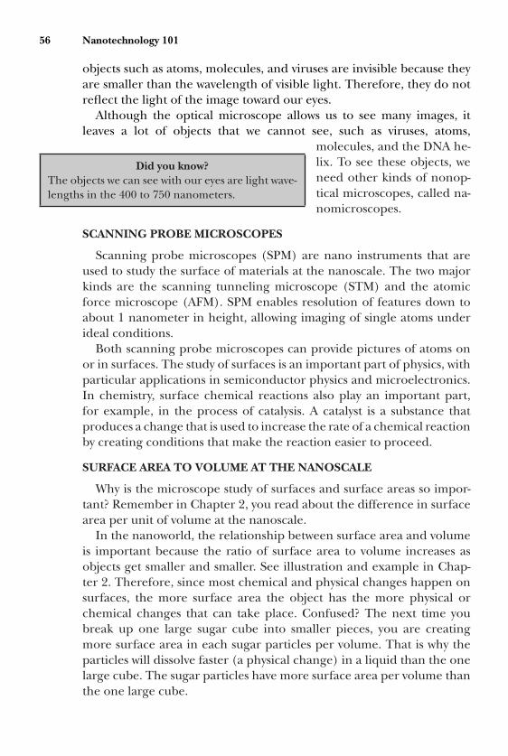
P1: 000
GGBD159C03 GR3880/Mongillo Top Margin: 5/8in Gutter Margin: 3/4in September 25, 2007 16:3
56 Nanotechnology 101
objects such as atoms, molecules, and viruses are invisible because theyare smaller than the wavelength of visible light. Therefore, they do notreflect the light of the image toward our eyes.
Although the optical microscope allows us to see many images, itleaves a lot of objects that we cannot see, such as viruses, atoms,
Did you know?The objects we can see with our eyes are light wave-lengths in the 400 to 750 nanometers.
molecules, and the DNA he-lix. To see these objects, weneed other kinds of nonop-tical microscopes, called na-nomicroscopes.
SCANNING PROBE MICROSCOPES
Scanning probe microscopes (SPM) are nano instruments that areused to study the surface of materials at the nanoscale. The two majorkinds are the scanning tunneling microscope (STM) and the atomicforce microscope (AFM). SPM enables resolution of features down toabout 1 nanometer in height, allowing imaging of single atoms underideal conditions.
Both scanning probe microscopes can provide pictures of atoms onor in surfaces. The study of surfaces is an important part of physics, withparticular applications in semiconductor physics and microelectronics.In chemistry, surface chemical reactions also play an important part,for example, in the process of catalysis. A catalyst is a substance thatproduces a change that is used to increase the rate of a chemical reactionby creating conditions that make the reaction easier to proceed.
SURFACE AREA TO VOLUME AT THE NANOSCALE
Why is the microscope study of surfaces and surface areas so impor-tant? Remember in Chapter 2, you read about the difference in surfacearea per unit of volume at the nanoscale.
In the nanoworld, the relationship between surface area and volumeis important because the ratio of surface area to volume increases asobjects get smaller and smaller. See illustration and example in Chap-ter 2. Therefore, since most chemical and physical changes happen onsurfaces, the more surface area the object has the more physical orchemical changes that can take place. Confused? The next time youbreak up one large sugar cube into smaller pieces, you are creatingmore surface area in each sugar particles per volume. That is why theparticles will dissolve faster (a physical change) in a liquid than the onelarge cube. The sugar particles have more surface area per volume thanthe one large cube.

P1: 000
GGBD159C03 GR3880/Mongillo Top Margin: 5/8in Gutter Margin: 3/4in September 25, 2007 16:3
The Nanotechnology Tool Box 57
Scanning Tunneling Microscopes (STM)
The first scanning probe instrument was the scanning tunneling mi-croscope (STM). The scanning tunneling microscope (STM) can showthree-dimensional images of individual atoms at the surface.
Gerd Binnig and Heinrich Rohrer of IBM’s Zurich Laboratory inZurich, Switzerland invented this microscope in 1981. The two scientistsreceived a Nobel Prize in Physics in 1986 for their innovation of the STM.
How Does the STM Work?
Scanning tunneling microscope (STM) uses a probe (the tip) to moveover the surface of the material being studied.
The tip of the probe, usually composed of tungsten or platinum, isextremely sharp. The tip, which consists of a single atom, is attached tocantilever that looks like a toy diving board with a sharp tip under oneend of it.
The tip slowly scans across the surface at a distance of only an atom’sdiameter. The tip is raised and lowered in order to keep the signal con-stant and maintain the distance. A small force measures the attraction orrepulsion between the tip and the surface of the sample during scanning.These forces, causing an up and down movement of the cantilever, aremonitored by a laser beam reflecting off the cantilever surface. Record-ing the up and down movement of the tip makes it possible to studythe structure of the surface sample. A profile of the wiggled surface iscreated, and from that a computer-generated image is produced. Thefinal image is a contour map of the surface showing trenches and valleys.The STM works best with conducting materials, but does not work wellwith insulators such as rubber.
The STM has many uses and applications in nanotechnology. TheSTM can image materials from DNA samples and other biological
Did you know?The Scanning Tunneling Microscope (STM) is verysensitive to vibrations. Just someone sneezing in thesame room, can jam the microscope’s tip into thesample and damage the experiment.
molecules. Another exam-ple is that STM has beenused to study the surfaceof operating battery elec-trodes through which elec-tricity enters or leaves.
Atomic Force Microscopes (AFM)
The atomic force microscope is sometimes called a Scanning ForceMicroscope. The AFM measures the interaction forces between probetip and sample.

P1: 000
GGBD159C03 GR3880/Mongillo Top Margin: 5/8in Gutter Margin: 3/4in September 25, 2007 16:3
58 Nanotechnology 101
Figure 3.1 How an AFM works. (Courtesy of Jeff Dixon)
How Does the AFM Work?
AFM is part of a family of instruments called scanning probe micro-scopes (SPM). AFM uses a probe moving across the sample’s surface toidentify its features. The probe is a sharp tip, usually made of silicon, atthe end of a cantilever that bends in response to the force between thetip and the sample being viewed. Any deflection from the sample is mea-sured and the AFM records the surface topography. The topography isthe projections (lumps), depressions (pits), and textures of a surface.The tip never touches the sample surface because it could damage it.AFMs are widely used to measure surface topography of many types ofsamples.
The atomic force microscope can be operated under two differentconditions (in air or in a vacuum) and two operating modes (contactor noncontact). Whatever the condition or mode, the basic operatingprinciples of the AFM remain the same. The AFM uses a probe thathas a tip mounted on a flexible cantilever. The tip is slowly scannedacross the surface of a material, just a few angstroms away from thesurface (noncontact mode) or in contact with it (contact mode). Anangstrom is one tenth (0.1) of a nanometer. The force between the

P1: 000
GGBD159C03 GR3880/Mongillo Top Margin: 5/8in Gutter Margin: 3/4in September 25, 2007 16:3
The Nanotechnology Tool Box 59
Table 3.1 Some Samples of Objects That Can BeObserved by an Atomic Force Microscope
Cells: Bacteria, PlantsCeramicsFiber: Hair, NanotubesMetalsMineralsMolecules: Self-Assembled Monolayers, ProteinsPaperParticles: Nanoparticles, Quantum DotsPlant Surfaces: Leaves, FruitPolymers
Note: AFM can image objects that are solid and have asurface.
atoms on the surface of the material and those on the tip cause the tipto deflect. This deflection can be recorded in various ways, the mostcommon of which uses a laser focused on the top of the cantileverand reflected onto photodetectors. A laser is a special type of ampli-fied light beam and is an essential part of CD and DVD players andrecorders.
The photodetector signals are used to map the surface topographyof samples with resolutions down to the nanoscale. At the nanoscale,the microscope is able to determine roughness, grain size, and features.
The number of applications for AFM has increased dramatically sincethe technology was invented in 1986. Presently, the AFM microscopes
Did you know?An angstrom is very small. An angstrom is a unit oflength equal to one-hundredth millionth of a cen-timeter or 10−8. Remember, a nanometer is 10−9.Chemists and physicists measure the distances inmolecules or wavelengths of light in angstroms.
are used for a variety ofapplications in industrialand scientific research thatincludes such areas as mi-croelectronics, telecommu-nications, biological, chem-ical, automotive, aerospace,and energy industries. Re-searchers also employ the AFM as a tool to investigate a wide rangeof materials such as thin and thick film coatings, ceramics, composites,glasses, synthetic and biological membranes, metals, polymers, and semi-conductors. The continuing application of the AFM systems will lead toadvancements in such areas as drug discovery, life science, electrochem-istry, polymer science, biophysics, and nano biotechnology.

P1: 000
GGBD159C03 GR3880/Mongillo Top Margin: 5/8in Gutter Margin: 3/4in September 25, 2007 16:3
60 Nanotechnology 101
In this activity, students are constructing the cantilever section of aLEGO R© model of a scanning probe microscope. LEGO R© models are builtto understand how a scanning probe microscope works. (Courtesy DeanCampbell)
The Advantages of AFM
The difference between AFM and other microscopy techniques isthe quality and the measure of resolution. While electron and opticalmicroscopes provide a standard two-dimensional horizontal view of asample’s surface, AFM also provides a vertical view. The resulting imagesshow the topography of a sample’s surface. While electron microscopeswork in a vacuum, most AFM modes work in dry or liquid environments.AFM does not require any special sample preparation that could damagethe sample or prevent its reuse.
AFM also can be used for imaging any conducting or nonconductingsurface properties of a substance, while the STM is limited to imagingonly conducting surfaces of a sample. The AFM is a major part of the$1 billion nanotechnology measurement tools market that is expectedto continue to grow at about 20 percent a year.

P1: 000
GGBD159C03 GR3880/Mongillo Top Margin: 5/8in Gutter Margin: 3/4in September 25, 2007 16:3
The Nanotechnology Tool Box 61
AFM Tips
AFM tips are generally made of silicon or silicon nitride. For mostapplications, pyramid-shaped silicon nitride tips are used. They are rel-atively durable and present a dry surface to the sample. Conical sili-con tips are often used for biomolecular applications because they arevery sharp and present a wet surface. However, they are relatively lessdurable.
Conventional silicon tips are good for measuring relatively flat sur-faces, but they do not penetrate the crevices that often exist in smalldevices and structures. The silicon tips also wear out quickly, reducingimage resolution.
Magnetic Force Microscopes
The magnetic force microscope (MFM) is another scanning probemicroscope. This microscope has a magnetic tip that is used to probethe magnetic field above the surface of a sample. The magnetic tip,mounted on a small cantilever, measures the magnetic interaction be-tween a sample and a tip. The MFM was developed as an evaluation toolfor measuring the magnetism levels in products.
INTERVIEW: NATHAN UNTERMAN
Mr. Nathan A. Unterman is a physics teacher at the GlenbrookNorth High School in Northbrook, Illinois. He teaches physics to highschool juniors and seniors. He and his students have built and usedLEGO R© models of the atomic force microscope (AFM) and the mag-netic force microscope (MFM). The author asked Mr. Unterman abouthow his interests in nanotechnology and his work in building LEGO R©
models.
How did you get interested nanotechnology?I attended a Research Experience for Science Teachers program in theMaterials Science department at Northwestern University a few yearsago.
Describe some of your experience in developing Lego models of anAtomic Force Microscope and a Magnetic Force Microscope.I was looking for a physical model that could be used in the class-room for scanning probe microscopes. I also wanted it to be somethingwhere quantitative data could be measured. The University of Wiscon-sin had a prototype for a LEGO R© AFM. I then created a method for

P1: 000
GGBD159C03 GR3880/Mongillo Top Margin: 5/8in Gutter Margin: 3/4in September 25, 2007 16:3
62 Nanotechnology 101
This is a completed LEGO R© model of a scanning probe microscope. Profes-sor Dean Campbell and other researchers conceptualize the idea of build-ing a model of a scanning probe microscope from LEGO R© building blocks.To construct the model, refer to instructions at the end of this chapter.(Courtesy Dean Campbell)
quantitative engagement. This engagement included the use of Excelsurface plotting.
How important is the field of nanotechnology in the subject you teach?In science in general, it is important. In secondary physics, it has not yetworked its way into the curriculum.
What advice would you give students who want to explore a career innanotechnology?Learn as much science, math, and writing as you can, and make sureyou balance that with the fine and applied arts.
Please describe how the LEGO R© model of the atomic forcemicroscope works.The probe is moved over a tray containing an array of balls that repre-sents the atoms of a sample. The beam from a laser pen in the probeis reflected off the cantilever of the probe as it scans points on the sur-face under study. The position of the reflected beam is measured ona wall-mounted grid and recorded. These positions are recorded in aspreadsheet and analyzed using the surface plot-graphing tool.

P1: 000
GGBD159C03 GR3880/Mongillo Top Margin: 5/8in Gutter Margin: 3/4in September 25, 2007 16:3
The Nanotechnology Tool Box 63
If a teacher or student wanted to construct the LEGO R© model of thescanning probe microscope, would you be able to assist them?They can refer to the article published in the December 2006 ScienceTeacher, or email me at: [email protected]
ELECTRON MICROSCOPES
Several different types of electron microscopes exist. Two majorones include the transmission electron microscopy (TEM) and the
� Measuring Electrical Properties with anElectron Force Microscope. ProfessorWendy Crone, Madison MetropolitanSchool District. http://mrsec.wisc.edu/Edetc/cineplex/MMSD/scanning3.html
scanning electron micro-scopy (SEM). Electron mi-croscopes use electronbeams instead of visiblelight, enabling resolution offeatures down to a few nano-meters.
Electron microscopes use a beam of high-energy electrons to probethe sample. Electron microscopes are scientific instruments that use abeam of highly energetic electrons to examine objects on a very finescale. High quality electron microscopes can cost from $250,000 to$1,000,000. They are one of the most useful instruments in laboratories.
A Scanning Electron Microscope
A scanning electron microscope (SEM) can analyze materials forinformation about topography, chemical composition, contamination,grain size and thickness with far greater depth of field than is possiblewith optical microscopy. The depth of field basically means how clear athree-dimensional image looks.
The topography information analyzed by the SEM includes the sur-face features of an object such as its texture and hardness. A microscopeoperator can observe the shape and size of the grain particles makingup the object and notice if there is any contamination. The compo-sition data includes the elements and compounds that the object iscomposed of. How the atoms are arranged in the pattern of the objectcan be detected by the crystallographic. The pattern in the crystal isformed by the way the atoms in a solid material are connected to oneanother.
ERNST ABBE
In the 1870s, a man named Ernst Abbe explained why the resolutionof a microscope is limited. He said that since the microscope uses visible

P1: 000
GGBD159C03 GR3880/Mongillo Top Margin: 5/8in Gutter Margin: 3/4in September 25, 2007 16:3
64 Nanotechnology 101
light and visible light has a set range of wavelengths, the microscopecan’t produce the image of an object that is smaller than the length ofthe light wave.
The Transmission Electron Microscope
The transmission electron Microscope (TEM) was the first type ofelectron microscope to be developed. It was developed by Max Knoll andErnst Ruska in Germany in 1931. The transmission electron microscope(TEM) operates on the same basic principles as the light microscopebut uses electrons instead of light. As mentioned earlier, what you cansee with a light microscope is limited by the wavelength of light. TEMsuse electrons as a “light source” and their much lower wavelength makesit possible to get a resolution a thousand times better than with a lightmicroscope. The enlarged version of the image of the specimen appearson a fluorescent screen or in a layer of photographic film.
You can see objects to the order of .2 nanometers. For example, youcan observe and study small details in the cell or other different materialsdown to near atomic levels. The microscope’s high magnification rangeand resolution has made the TEM a valuable tool in medical, biological,and materials research.
Transmission electron microscopy has had an important impact onthe knowledge and understanding of viruses and bacteria. The improve-ment in resolution provided by electron microscopy has allowed vi-sualization of viruses as the causes of transmissible infectious disease.Researchers are continuing the use of electron microscopy in the inves-tigation of such pathogens as SARS and the human monkeypox virus.SARS is a severe acute respiratory disease in humans which is caused bythe SARS virus. Monkeypox is a rare smallpox-like disease that is mostcommon in the rain forests of central and West Africa.
How Does the TEM Work?
A light source at the top of the microscope emits a beam of electronsthat travel through a vacuum in the column of the microscope. Insteadof glass lenses focusing the light source in the light microscope, theTEM uses electromagnetic lenses to focus the electrons into a very thinbeam. The electron beam then travels through the specimen you wantto study. Depending on the density of the material present, some of theelectrons are scattered and disappear from the beam. At the bottom ofthe microscope the rest of the electrons hit a fluorescent screen. Thescreen shows a shadow-like image of the specimen that can be studieddirectly by the operator or photographed with a camera.

P1: 000
GGBD159C03 GR3880/Mongillo Top Margin: 5/8in Gutter Margin: 3/4in September 25, 2007 16:3
The Nanotechnology Tool Box 65
Scanning Electron Microscope
The first Scanning Electron Microscope (SEM) debuted in the1940s but the first commercial instruments were produced in the1960s.
The SEM is a type of electron microscope capable of producing high-resolution images of a sample surface. Due to the manner in which theimage is created, SEM images have a characteristic three-dimensional ap-pearance and are useful for judging the surface structure of the sample.This scanning electron microscope has a magnification range from15xto 200, 000x and a resolution of 5 nanometers.
The SEM has the ability to image large areas of the specimen thatincludes thin films and bulky materials as well. In general, SEM imagesare much easier to interpret than TEM images.
SsBugscope
The Bugscope project is an educational outreach program for K-12 class-rooms. The project provides a resource to classrooms so that they mayremotely operate a scanning electron microscope to image “bugs” or “crea-tures” at high magnification. The microscope is remotely controlled in realtime from a classroom computer over the Internet using a Web browser.BugScope provides a state-of-the-art microscope resource for teachers thatcan be readily integrated into classroom activities. Students can peek at ex-treme close-up views of the insect world via their school computer labs andfor free.
The BugScope project was developed by the BugScope Project Teamand the Imaging Technology Group at the Beckman Institute for AdvancedScience and Technology at the University of Illinois at Urbana-Champaign.The scanning electron microscope costs about half a million dollars, andits main function is for research done at the university by graduate andpostdoctoral students as well as industry.
The team at the institute sets up preset views of the “creatures” providedby the school. The classroom teacher and students, from a computer stationat their own school, can operate the microscope for other views. Studentswatch the images projected on a screen in the front of the computer lab,and can use their own computer stations to ask questions from the scientistsat the center in Urbana.
The classroom has ownership of the project. The students design theirown experiments and provide their own bugs to be imaged in the micro-scope. Bugscope provides resources pages with helpful links related toelectron microscopy and bugs. The BugScope Web site: http://bugscope.beckman.uiuc.edu/
P1: 000
GGBD159C03 GR3880/Mongillo Top Margin: 5/8in Gutter Margin: 3/4in September 25, 2007 16:3
66 Nanotechnology 101
Bugscope also offers a virtual microscope activity. They recently devel-oped a Virtual Microscope that allows for Bugscope-type viewing (withoutan Internet connection) from precaptured high-resolution image datasets.They have built both a Virtual Scanning Electron Microscope (Virtual SEMor VSEM) and a Virtual Light Microscope (VLM). Go to their Web site anddownload the Virtual Microscope and give it a try for free!
Ss
HITACHI TABLETOP MICROSCOPE
Hitachi has developed its first tabletop electron microscope, the TM-1000. The TM-1000 is designed for researchers who want to breakthrough the limits of the light microscopy and close up to sophisticatedmagnifications up to 10,000.
The microscope is compact, easy to use, is ideal for a wide varietyof applications, and has superior resolution for higher magnificationthan an optical microscope. The TM-1000 provides a real alternativeto optical microscopes, stereomicroscopes, and confocal laser scanningmicroscopes. It has applications for many areas including life science,food, cosmetics, health care, pharmaceutical, textiles, materials science,semiconductor, and education.
NANOFABRICATION CLEANROOM FACILITIES
Scientists need a dust-free workspace to use electron microscopesand other tools effectively to build small-scale circuits and machines.The workspace facility is called a cleanroom and it is an important partof nanotechnology research. In fact it is nearly impossible to conductnanoscale research without a cleanroom environment.
Why a cleanroom? On the scale of a nanometer, any particle that is300 nanometers is huge and is capable of causing short circuits in ananoscale electronic circuit.
Cleanroom environments can cost approximately 3 million dollarsto install. Most cleanrooms consist of an air filtration system as well astemperature and humidity control systems. The system constantly movesthe air down to the floor where it is sucked back into the return air systemand then cleaned and sent back into the room. Some cleanrooms haveyellow illumination that allows researchers to work with light sensitivematerials. The yellow illumination prevents light-sensitive material frombeing exposed to ultraviolet light.
As researchers enter the cleanroom, special equipment removes dirtand dust particles from their shoes. The researchers then put on safetyglasses, gloves, and coveralls over their street clothes, shoes, and hair.All of the garments are made from lint-free fabrics that are antistatic. It

P1: 000
GGBD159C03 GR3880/Mongillo Top Margin: 5/8in Gutter Margin: 3/4in September 25, 2007 16:3
The Nanotechnology Tool Box 67
The Scanning Electron Microscope (FE-SEM) Model S-5500 is producedby Hitachi High-Technologies Corporation. The capabilities of the instru-ment bridge many research fields that include pharmaceutical, biological,and food industry research and nanomanipulation devices for advancedcarbon nanotube research. (Courtesy Hitachi High-Technologies Corporation(Japan))
may take 40 steps or more to complete the steps needed to get dressedbefore entering the cleanroom. Most of us get up in the morning usingbetween 6 and 9 steps to get dressed.
SCANNING ELECTRON MICROSCOPESAND PHOTOLITHOGRAPHY
Today the scanning electron microscope is mainly used for the studyof surfaces of materials as well as for the investigation of transpar-ent specimens. Two major applications for the scanning electron mi-croscope are for analyzing and inspecting objects and for photolitho-graphy.

P1: 000
GGBD159C03 GR3880/Mongillo Top Margin: 5/8in Gutter Margin: 3/4in September 25, 2007 16:3
68 Nanotechnology 101
Figure 3.2 Photolithography. (Courtesy of Jeff Dixon)
Photolithography is a process used to build components on amicrometer-sized scale. The process uses light to transfer a pattern of say,a microchip part, from a mask to a light-sensitive chemical photoresistthat forms an image of the pattern on a substrate. The method is likeusing silk-screening to make pictures and images from pattern maskson T-shirts. Photolithography has a broad range of industrial applica-tions, including the manufacture of semiconductors, flat-panel displays,micromachines, and disk heads.
NANO-IMPRINT LITHOGRAPHY
Today several companies are researching and experimenting withdifferent kinds of lithographic techniques using nanotechnology. Twotechniques include Dip Pen Nanolithography and Thermal Dip PenNanolithography.
Dip Pen Nanolithography
Dip Pen Nanolithography (DPN) is a soft-lithography technique thatuses an AFM scanning probe tip to draw nanostructures. In the DPNprocess, a probe tip is coated with liquid ink, which then flows onto the

P1: 000
GGBD159C03 GR3880/Mongillo Top Margin: 5/8in Gutter Margin: 3/4in September 25, 2007 16:3
The Nanotechnology Tool Box 69
surface to make patterns wherever the tip makes contact. This direct-write technique offers high-resolution patterning capabilities for a num-ber of molecular and biomolecular “inks” on a variety of substrates.Substrates are the base material that the images are printed on.
Some of the applications of the DPN technique include sol gel tem-plates that are used to prepare nanotubes and nanowires, and proteinnanoarrays to detect the amount of proteins in biological samples suchas blood.
Thermal Dip Pen Nanolithography
Researchers from the Georgia Institute of Technology and the NavalResearch Laboratory (NRL) have developed another method for writingnanometer-scale patterns onto a variety of surfaces.
Their writing method is called thermal dip pen nanolithography,which is an extension for dip pen nanolithography. The tDPN method
Did you know?The use of low-temperature, scanning electron mi-croscopy can be used by ski-run operators to deter-mine how effective their artificial snow operationsare in lengthening the ski season because of thecontrast between artificial and natural snow crys-tals.
uses easily melted solid inksand special AFM probes.The probes have built-inheaters that allow writing tobe turned on and off at will.The tDPN could be used toproduce features too smallto be formed by light-basedlithography. Other applica-tions of the tDPN include using the process as a soldering iron forrepairing circuitry on semiconductor chips. The thermal materials alsoprovide sharper features because they do not spread out like liquid inks.
NASA VIRTUAL LAB
How would you like to learn how to use an electron microscope in avirtual lab? Besides the BugScope project, NASA provides a virtual labonline of an electron microscope for schools, pupils, and teachers. Thefree JAVA program allows users a good sense of what the instrument cando. By downloading the free JAVA program for both PC and Mac, userscan pan, zoom, and even use a built-in ruler to measure such items as abeetle’s leg, crystals from a human kidney stone, and other objects.
Virtual Lab completely emulates a scanning electron microscope andallows any user to zoom and focus into a variety of built-in microscopicsamples. It also comes with a set of educational materials such as a demoon how a SEM works and movies of the real thing in action.
The Virtual Microscope, which includes free downloading, is availableon Sourceforge, http://virtual.itg.uiuc.edu/training/

P1: 000
GGBD159C03 GR3880/Mongillo Top Margin: 5/8in Gutter Margin: 3/4in September 25, 2007 16:3
70 Nanotechnology 101
See Chapter 9 for more information about the NASA Virtual Micro-scope Web site.
NANOMANIPULATORS
One of the major goals in the future is to manufacture products atthe nanoscale. In order to achieve that goal, researchers will need to usetools that can grab, pickup, push, pull, turnover, tap down, stack, andmove atoms and molecules. To develop the tools needed to do this kindof work will take more research time.
For now, nanotechnololgists are using and are continuing to developnew nanomanipulators—tools to manipulate objects in nanometers.Nanomanipulators are and will be important tools in nanotechnologyresearch and development,
Presently, scanning probe microscopy, such as the atomic force mi-croscope and the scanning tunneling microscope, is one method tomanipulate objects in nanometers. As an example, the AFM have beenused to move atoms, carbon nanotubes, and to test electronic circuitboards and integrated circuits.
A few companies are providing add-ons or interfaces to scanningprobe microscopes such as scanning tunneling microscopes (STM) andatomic force microscopes (AFM). Medical researchers have used a spe-cial kind of nanomanipulator to study fibrin fibers, the major com-ponents of blood clots. The researchers hope to gain insight into thehealing process by observing the strength and mechanical properties ofblood clots under a variety of conditions.
One company has a kind of nanomanipulator that offers several po-sitions that grasp, move, and test nanoscale samples. This action allowssimultaneous manipulation, imaging, and testing of samples.
NANOFABRICATION
Nanomanipulation will play a big role in nanofabrication. Nanofab-rication is the design and manufacture of devices with dimensions
Did you know?The microprocessor or microchip starts up andgoes to work when the computer is turned on. Itperforms arithmetic and logic operations that re-spond to and process basic instructions that drivethe computer.
measured in nanometers.Nanofabrication is of in-
terest to computer engi-neers who are interested inresearching and building su-per high-density micropro-cessors that can be used inlarge computer mainframes, microcomputers, and in handheld com-puters. The goal is to be able to get each data bit stored in a single atom.

P1: 000
GGBD159C03 GR3880/Mongillo Top Margin: 5/8in Gutter Margin: 3/4in September 25, 2007 16:3
The Nanotechnology Tool Box 71
If it can be done, a single atom might even be able to represent a byteor word of data.
Nanofabrication has also caught the attention of the medical industry,the military, and the aerospace industry. Nanofabrication methods in thelines of miniaturization (top-down) and self-assembly (bottom-up) areessential for the development of nanotechnology.
Top-down fabrication can be likened to making a baseball bat from ablock of wood. The original block of wood is cut down until the desiredshape of the bat is achieved. That is, you start at the beginning or thetop and slowly work your way down removing any wood in the shapingof the bat that is not needed.
The most common top-down approach to fabrication involves litho-graphic patterning techniques mentioned earlier in this chapter. Thelithographic process uses short-wavelength light sources.
A major advantage of the top-down approach is that the parts are bothpatterned and built in place, so that no assembly step is needed.
Bottom-up nanofabrication is the opposite of top-down nanofabrica-tion. The bottom-up nanofabrication is to build nanostructures atomby atom using either self-assembly techniques or manipulating atoms byemploying scanning probing microscopy.
Now many industries are adapting nanofabrication technology andwill use it even more in the future. Some of the companies include thosethat produce fiber-optic communications, pharmaceuticals, and micro-electronics. According to the Federal Government, the unprecedentedspread of nanofabrication and nanotechnology is likely to change theway almost everything is manufactured—from vaccines to computers toautomobile tires to objects not yet discovered.
NANO INTERVIEW: ASSOCIATE PROFESSOR DEAN CAMPBELL,Ph.D., BRADLEY UNIVERSITY
Dean Campbell, Ph.D., is an associate professor of chemistry atBradley University in Peoria, Illinois. Dr. Campbell talked with the au-thor of Nanotechnology 101 about the booklet, Exploring the Nanoworldwith LEGO R© Bricks, scanning probe microscopy, and ideas for building aLEGO R© model of a scanning probe microscope.
What college did you attend and what was your major field?I earned my bachelor’s degree in chemistry from the University ofWisconsin-Green Bay and my Ph.D. in chemistry from NorthwesternUniversity.

P1: 000
GGBD159C03 GR3880/Mongillo Top Margin: 5/8in Gutter Margin: 3/4in September 25, 2007 16:3
72 Nanotechnology 101
Dean Campbell, Ph.D., teaches chemistryat Bradley University in Peoria, Illinois.(Courtesy Duane Zehr)
How did you get interestedin nanotechnology?When I was an undergraduate, I wasinvolved in a project studying the sur-face chemistry of coal ash particles,and I was intrigued by how the chem-istry of surfaces could be so differ-ent from bulk material. In graduateschool I worked with surfaces of a dif-ferent sort, self-assembled monolay-ers. These types of monolayers are arather simple form of nanotechnol-ogy, as they tend to have nanoscalethicknesses.
What were your favorite subjectsin high school?I liked a lot of the sciences, be-cause I like to understand how thingswork. Ironically, because I was slow in
chemistry lab, I thought in high school that I would go into any sci-ence field EXCEPT chemistry. I changed my mind as an undergraduatebecause the field was so interesting and employable.
What is scanning probe microscopy (SPM)?Scanning probe microscopy (SPM) is a method for mapping surfaceforces of materials on the atomic scale. By mapping these forces, muchcan be learned about the surfaces of materials, where many interestingand complex phenomena occur. For example, many chemical reactionsinvolving solids are dependent on the nature of their surfaces. Scanningprobe microscopy includes the methods of atomic force microscopy(AFM), magnetic force microscopy (MFM), and lateral force microscopy(LFM). Most force microscopy techniques are variations of the samebasic principle. Forces between the surface and a cantilever tip causethe tip to deflect up and down or sometimes side to side. Deflection ofthe cantilever shifts the position of a laser beam that reflects off the topof the cantilever onto a photodiode array. The movement of the beambetween the photodiodes is used to calculate the cantilever deflection.
How is a scanning probe microscope useful in nanotechnologyresearch and in nanofabrication?The technique is primarily used to map surface forces at the nanoscale,but the SPM probes have sometimes been used to move objects such asatoms or “write” with molecular “ink.”

P1: 000
GGBD159C03 GR3880/Mongillo Top Margin: 5/8in Gutter Margin: 3/4in September 25, 2007 16:3
The Nanotechnology Tool Box 73
How is the scanning probe microscope different from an atomic forcemicroscope?An atomic force microscope can be considered one type of scanningprobe microscopy. Several other types of SPM exist (see: http://en.wikipedia.org/wiki/Scanning probe microscopy)
How did you and other researchers conceptualize the idea of buildinga model of a Scanning Probe Microscope from LEGO R© buildingblocks? Did you try other building materials as well?A number of people have used different materials to demonstrate SPM,including wooden sticks, hacksaw blades, and flexible sheet refrigeratormagnets. We opted to use LEGO R© bricks for a number of reasons.
First, many people are familiar with LEGO R© bricks, and most modelscan be built with a level of mechanical sophistication that does not in-timidate or frustrate the user. Second, LEGO R© bricks typically have manyconnection points, allowing tremendous flexibility in the structures thatcan be built. A set of bricks can be used to model structures of matterand the techniques used to study them.
You have taught students how to build a scanning probe microscopemodel from LEGO R©blocks. How old were the students who built theLEGO R© model and how long did it take them to build it? Were thereany problems in building the model?Eighth graders as well as graduate students have built various creationsof models. The simplest models can be built within a half hour. Morecomplicated models take longer to build. The most challenging part ofbuilding the model appears to be mounting the laser pointer.
If a teacher or student wanted to construct the LEGO R© model of thescanning probe microscope, whom should they contact for directionsand for a list of materials?Most of the directions for making the model are in the online book,“Exploring the Nanoworld with LEGO R© Bricks,” which can be accessedfrom http://mrsec.wisc.edu/Edetc/LEGO/index.html.
My contact information given on the site is:Dr. Dean Campbell, Department of Chemistry, Bradley University,
1501 West Bradley University, Peoria, IL 61625. Phone: (309) 677-3029.E-mail: [email protected]
What would your advice be to young people who would be interested ina career in nanotechnology? What are some of the opportunities in thisfield?Nanotechnology is a hot field now and will likely remain so for sometime. Nanotechnology is also a very interdisciplinary field. Successful

P1: 000
GGBD159C03 GR3880/Mongillo Top Margin: 5/8in Gutter Margin: 3/4in September 25, 2007 16:3
74 Nanotechnology 101
individuals will need to have a breadth of knowledge in mathematics,physical sciences and biology, as well as the ability to communicateeffectively with others.
What are some of the benefits of nanotechnology and what would besome of the risks?Many technologies stand to benefit from nanotechnology, ranging fromcomputers to medicine to sunscreen. There are some concerns thatnanoscale chemicals will have different properties and therefore differ-ent toxicities than bulk materials. Therefore, nanostructures must becarefully assessed for potential unexpected hazards.
NANO ACTIVITY: MODELING A SCANNING PROBE MICROSCOPE
In this activity, Professor Campbell provides background informationabout Scanning Probe Microscopy (SPM) and ideas on how to build aLEGO R© model of it.
Background Information. Scanning Probe Microscopy
You are likely familiar with microscopes that use light, but manyobjects like atoms are too small to be seen using light. Other micro-scopes use electrons to view even smaller objects, but these also havedifficulty visualizing objects as small as atoms.
Scanning probe microscopy (SPM) is a method for mapping sur-faces of materials on the atomic scale. It is useful to study the locationsof atoms on surfaces because many chemical reactions, such as corro-sion and catalysis, take place at solid surfaces. Most SPM techniquesare variations of the same basic principles, illustrated in the picture.At the heart of the microscope is a probe called a cantilever. Thecantilever is fixed at one end and can flex up and down at the otherend like a diving board. A laser beam is shined onto the tip of the can-tilever. The light bounces off the top of the cantilever onto a patternof light sensors called a photodiode array.
To run the SPM, the cantilever is brought very close to a surface.The surface is moved back and forth under the cantilever, so thecantilever more or less scans the surface. Forces between the surfaceand a cantilever tip cause the tip to deflect up and down. Deflectionof the cantilever shifts the position of the laser beam that reflects offthe top of the cantilever onto a photodiode array. The movement ofthe beam between the photodiodes is used to measure the amountof cantilever deflection. A computer combines the information

P1: 000
GGBD159C03 GR3880/Mongillo Top Margin: 5/8in Gutter Margin: 3/4in September 25, 2007 16:3
The Nanotechnology Tool Box 75
about the cantilever deflection with information about the back andforth movement about the surface to produce a three-dimensionalmap of the surface. This SPM technique is so sensitive that in-dividual atoms can deflect the cantilever probe and therefore bedetected!
Directions for Building the Model
Most of the directions for making the model can be accessedat our Web site “Exploring the Nanoworld with LEGO R© Bricks,”http://mrsec.wisc.edu/Edetc/LEGO/index.html.
To get an idea of how your model will look when finished, observethe triangular LEGO R© model in the photo. This model contains alaser pointer and a cantilever with a triangular LEGO R© probe on itsunderside and a mirror atop it. In this model, the cantilever tip isin physical contact with a LEGO R© surface. The LEGO R© pegs on thesurface deflect the cantilever. Light from the pocket laser reflectsfrom the mirror on the cantilever and shines onto a wall.
After you build your model, have someone attach small bricks tothe LEGO surface and then place the SPM behind a screen. Usingthe laser beam spot movement and horizontal surface movement, tryto map the locations of the small bricks on the surface. Sketch yourmap of the surface on a sheet of paper.
Placing 1x1 bricks on a flat plate “substrate” makes raised bumps topush the cantilever (and the laser beam spot) up and down. A “han-dle” can be attached to this substrate and used to map to positions ofthe bumps. Place the SPM and substrate on a sheet of paper. Move thesubstrate back and forth (with the handle always pointing in the samedirection). When a bump pushes the beam spot up, make a mark onthe paper at the end of the handle. Note that the map produced willbe rotated 180O from the actual bump positions.
Questions to Explore
1. Will a bump on a flat surface move the laser spot up or down?2. How does the distance the SPM is positioned from the wall affect how
much the laser beam spot shifts?
READING MATERIALS
Drexler, Eric K. Nanosystems: Molecular Machinery, Manufacturing, and Computation.New York: John Wiley & Sons, 1992.

P1: 000
GGBD159C03 GR3880/Mongillo Top Margin: 5/8in Gutter Margin: 3/4in September 25, 2007 16:3
76 Nanotechnology 101
Fritz, Sandy. Understanding Nanotechnology: From the Editors of Scientific American. NewYork: Warner Books, 2002.
Hall, J. Storrs. Nanofuture: What’s Next For Nanotechnology. Amherst, NY: PrometheusBooks, 2005.
Newton, David E. Recent Advances and Issues in Molecular Nanotechnology. Westport,CT: Greenwood Press, 2002.
Scientific American (authors). Key Technologies for the 21st Century: Scientific American:A Special Issue. New York: W.H. Freeman & Co, 1996.
VIDEOS
Try the Simulator. To see a simulation of a scanning tunnel microscope go to:http://nobelprize.org/educational games/physics/microscopes/scanning/
Videos from the Hitachi Corporation, http://www.hitachi.com/about/corporate/movie/ What’s Next in Nanotechnology?
Penn State University. Amazing Creatures with Nanoscale Features: This animation is anintroduction to microscopy, scale, and applications of nanoscale properties. Thisactivity is available for use via the Center Web site at http://www.cneu.psu.edu/edToolsActivities.html
Electron-Beam Lithography. Nanopolis Online Multimedia Library. Electron-beamlithography is a technique for creating extremely fine patterns required for modernelectronic circuits. http://online.nanopolis.net/viewer.php?subject id=139
NanoManipulator: Seeing and Touching Molecules. http://www.nanotech-now.com/multimedia.htm
Video Zyvex. Nanomanipulator, Zyvex S100 DVD Preview. http://www.zyvex.com/Research/SEM manip/Manip.html
WEB SITES
Scanning Tunneling Microscope (STM): Describes the STM’s development.http://physics.nist.gov/GenInt/STM/stm.html
Scanning Probe Methods Group, University of Hamburg: Academic research groupusing scanning probe methods (SPM), emphasis on investigating the relationshipbetween nanostructure and nanophysical properties. http://www.nanoscience.de/
IBM Almaden STM Molecular Art: Some of the famous images of atoms andmolecules made with IBM’s scanning tunneling microscope. http://www.almaden.ibm.com/vis/stm/lobby.html
NanoManipulator: University of North Carolina—The NanoManipulator providesan improved, natural interface to SPMs (STMs and ATMs). http://www.cs.unc.edu/Research/nano/index.html
Exploring the Nanoworld. http://mrsec.wisc.edu/edetc.
The Incredible Shrunken Kids. http://www.sciencenewsforkids.org/articles/20040609/Feature1.asp

P1: 000
GGBD159C03 GR3880/Mongillo Top Margin: 5/8in Gutter Margin: 3/4in September 25, 2007 16:3
The Nanotechnology Tool Box 77
SOMETHING TO DO
You can create an edible, layered cookie (nanosmore) that will representthe process of photolithography by creating a patterned silicon wafer us-ing a substrate and a photoresist with simple foods. www.nbtc.cornell.edu/mainstreetscience/nanosmores and photolithography.pdf

P1: 000
GGBD159C03 GR3880/Mongillo Top Margin: 5/8in Gutter Margin: 3/4in September 25, 2007 16:3

P1: 000
GGBD159C04 GR3880/Mongillo Top Margin: 5/8in Gutter Margin: 3/4in September 25, 2007 16:3
4
Carbon Nanotubes,Nanowires, andNanocrystals
Carbon is one of the most abundant elements in living things and ma-terials derived from living things. By volume, carbon is about the fourthmost abundant element in the universe.
As you learned in Chapter 2, elements are types of atoms that make upall the things around us. Carbon plays an important role in nanotech-nology research and for potential nanotechnology applications. Beforewe discuss the role of carbon as nanoparticles, let’s review some generalinformation about the chemical and physical properties of carbon inthe macro-world.
THE ELEMENT CARBON
The chemical element carbon (C), is found in many different com-pounds. It is in the food we eat, the clothes we wear, the cosmeticswe use, and the gasoline that fuels our cars. Carbon plays a domi-nant role in the chemistry of life and without carbon we could notexist.
Carbon is a naturally occurring nonmetallic element that is presentin the cells of all organisms. Carbon has an atomic number of 6and an atomic weight of 12. The carbon atom contains six neutronsand six protons and combines with other elements forming a vari-ety of compounds that include carbon dioxide and carbon mono-xide.
Carbon makes up about 19 percent of the mass of the human body andis an essential component of proteins, carbohydrates, fats, and nucleicacids. All fossil fuels, coal, petroleum, oil shale, and natural gas, containcarbon as a principal element and combined with hydrogen form acategory of hydrocarbons.

P1: 000
GGBD159C04 GR3880/Mongillo Top Margin: 5/8in Gutter Margin: 3/4in September 25, 2007 16:3
80 Nanotechnology 101
Figure 4.1 Carbon Atom. (Courtesy of Jeff Dixon)
Products Made from Carbon
As noted, carbon can combine with other elements as well as withitself. This ability allows carbon to form many different compounds ofvarying size, strengths, and shape. Carbon is used in synthetic mate-rials called composites that contain both carbon fiber and fiberglassreinforcement.
Light yet strong, carbon composites have many applications inaerospace and automotive fields, as well as in sailboats, and notablyin modern bicycles. Carbon is also becoming increasingly common insmall consumer goods as well, such as laptop computers, tripods, fishingrods, tennis racket frames, stringed instrument bodies, classical guitarstrings, and even drum shells.
Some Uses of Carbon
Graphite combines with clays to form the “lead” used in pencils.
A diamond is used for decorative purposes, and also as drill bits.
Carbon is added to iron to make steel.
Carbon in the form of graphite is used for control rods in nuclear reactors.
Graphite carbon in a powdered cake form is used as charcoal for cooking,artwork, and other uses.
Charcoal (carbon)is a constituent of gunpowder.

P1: 000
GGBD159C04 GR3880/Mongillo Top Margin: 5/8in Gutter Margin: 3/4in September 25, 2007 16:3
Carbon Nanotubes, Nanowires, and Nanocrystals 81
Charcoal pills are used in medicine in pill or powder form to adsorb toxinsor poisons from the digestive system.
Different Forms of Carbon
There are several different allotropes or forms of carbon. Each formhas a different molecular structure. The forms include amorphous,graphite, diamond, and fullerene.
The term amorphous means lacking a definite form or having no spe-cific shape. In chemistry, the term amorphous means that the substanceis lacking a crystalline form. For example, soot is an amorphous carbonthat is a dark powdery deposit of unburned fuel residues. Glass, amber,wax, rubber, and plastics are other examples of amorphous substances.Amorphous carbon has been found in comets.
However, the other forms of carbon—diamonds, graphites, andfullerenes—have definite crystalline forms. Graphite is a very soft min-eral consisting of loosely bond atoms arranged in a two-dimensionalcrystalline form that looks like a thin flat plane. This property makesgraphite a good natural lubricant because it’s flat, planar structure al-lows the nanoscale sheets of graphite to slide past one another eas-ily. Although the mineral is soft, graphite’s strength and its abilityto conduct electricity makes the mineral especially useful in nano-technology.
There are two main classifications of graphite, natural and synthetic.Graphite minerals can be found naturally in the Earth’s crust. Syntheticgraphite is made from petroleum coke.
Besides pencil production, graphite is also used to manufacture cru-cibles, ladles, and moulds for containing molten metals. Graphite ismainly used as electrical material in the manufacturing of carbonbrushes in electric motors. Highly pure graphite is used in large amountsfor the production of moderator rods and other components in nuclearreactors. The moderator in the nuclear reactor is used to slow downthe neutrons so that the right speed is maintained for a steady fissionrate.
Some other uses of graphite include:
� Aerospace applications� Batteries� Carbon brushes� Graphite electrodes for electric arc furnaces for metallurgical processing.� Graphite lubricants

P1: 000
GGBD159C04 GR3880/Mongillo Top Margin: 5/8in Gutter Margin: 3/4in September 25, 2007 16:3
82 Nanotechnology 101
Diamond
The hardest known natural mineral is diamond. The diamond con-tains carbon atoms that are stacked or arranged in a three-dimensionalform or array. This structure makes the diamond super hard for thecutting and grinding of metals and other materials. Unlike graphite, adiamond is not a good conductor of electricity but the mineral is anexcellent thermal conductor.
Applications of diamonds are used in a variety of products that in-clude laser diodes and small microwave power device, integrated circuitsubstrates, and printed circuit boards. Diamond is starting to be usedin optical components, particularly as a protective coating for infraredoptics in harsh environments.
Diamond provides an impressive combination of chemical, physical,and mechanical properties: Some of these properties include:
� Low coefficient of friction� High thermal conductivity� High electrical resistance� Low thermal expansion coefficient
FULLERENES AND NANOTECHNOLOGY
Fullerenes are the third allotropic form of carbon material (aftergraphite and diamond). Fullerenes are large molecules of carbon that
Did you know?Another allotrope of carbon is a spongy solidthat is extremely lightweight and, unusually, at-tracted to magnets. The inventors of this new formof carbon—a magnetic carbon nanofoam—say itcould someday find medical applications.
are arranged in a form thatlooks much different fromthe shapes of graphite ordiamond. Fullerenes are ar-ranged in a form that isspherical, ellipsoid, or cylin-drical. Fullerenes are about1 nanometer in diameter.
This compares to 0.16 nanometer for a water molecule.Fullerenes were discovered during laser spectroscopy experiments at
Rice University in September 1985. The 1996 Nobel Prize in Chem-istry was awarded to Professors Robert F. Curl, Jr., Richard E. Smalley,and Sir Harold W. Kroto for their discovery. Fullerenes were namedafter Richard Buckminster Fuller, an architect known for the design ofgeodesic domes, which resemble spherical fullerenes in appearance.

P1: 000
GGBD159C04 GR3880/Mongillo Top Margin: 5/8in Gutter Margin: 3/4in September 25, 2007 16:3
Carbon Nanotubes, Nanowires, and Nanocrystals 83
BUCKYBALLS
By far the most common and best-known fullerene is the buckmin-sterfullerene, buckyball, or C60. It has a soccer-ball-shaped structure
� To watch and listen to Sir Harold Krotoexplain why he named the carbon clusterthat he discovered, buckminsterfullerene,go to: http://online.nanopolis.net/viewer.php?subject id=268]
that includes 20 hexagonsand 12 pentagons. Scientistshave now discovered otherbuckyballs as well. They in-clude C70, C76, and C84.
Applications of Buckyballs
The fullerene family of carbon molecules possesses a range of uniqueproperties. A fullerene nanotube has tensile strength about 20 times
Did you know?Rice University scientists had constructed theworld’s smallest car—a single molecule “nanocar”that contained a chassis, axles, and four buckyballwheels. The entire car measured just 3–4 nanome-ters across, making it slightly wider than a strand ofDNA.
that of high-strength steelalloys, and a density halfthat of aluminum. So itis stronger than steel andlighter than aluminum.
Since the discovery of full-erenes, scientists have dis-covered some possible usesfor these molecules. Some ofthese potential applications include being used in making computers,fuel cells, and sensors.
Major pharmaceutical companies are exploring the use of fullerenesin drugs to control the neurological damage of such diseases asAlzheimer’s disease and Lou Gehrig’s disease (ALS). Companies arealso testing the use of fullerenes in drugs for atherosclerosis and for usein antiviral agents.
A group of medical researchers believe that fullerenes could be usedin tiny special sponges that would soak up dangerous chemicals fromany tissues in the brain that have been injured. The sponges would im-mobilize the dangerous chemicals that would, if left untreated, destroythe nerve cells.
CARBON NANOTUBES
Scientists discovered that if you can make buckyballs big enough, theycould become carbon cylinders called carbon nanotubes. Carbon nan-otubes are long, thin cylinders of carbon molecules. A carbon nanotubeis a completely different material from either diamond or graphite.

P1: 000
GGBD159C04 GR3880/Mongillo Top Margin: 5/8in Gutter Margin: 3/4in September 25, 2007 16:3
84 Nanotechnology 101
Figure 4.2 Carbon Forms. (Courtesy of Jeff Dixon)
Sumio Iijima, of NEC Corporation came upon carbon nanotubes in1991 in Tsukuba, Japan, while researching buckyballs using an electronmicroscope. The carbon nanotubes he discovered can be visualized asa two-dimensional sheet of graphite. The arrangement of carbon atomsinto a hexagonal lattice is called “graphene,” because it has the formof a graphite sheet rolled into a cylinder. The nanotube looks like arolled-up piece of chicken wire.
Carbon nanotubes have unique properties that make them poten-tially useful in a wide variety of applications such as in nanoelectronics,optics, and materials applications. They exhibit extraordinary strengthand unique electrical properties, and are efficient conductors ofheat.

P1: 000
GGBD159C04 GR3880/Mongillo Top Margin: 5/8in Gutter Margin: 3/4in September 25, 2007 16:3
Carbon Nanotubes, Nanowires, and Nanocrystals 85
Two Types of Nanotubes
There are two main types of nanotubes: single-walled nanotubes(SWNTs) and multiwalled nanotubes (MWNTs).
Most SWNTs have a diameter of close to 1 nanometer, with a tubelength that can be many thousands of times longer. In fact, SWNTscan reach the length of centimeters. The structure of a SWNT can beconceptualized by wrapping a one-atom-thick layer of graphite calledgraphene into a cylinder. A graphene is a two-dimensional single sheetof carbon-bonded atoms.
A single-walled nanotube is commonly called a buckytube and con-sists of one single shell. The nanotube is cylindrical, with at least oneend typically capped with a hemisphere of the buckyball structure. Thediameter of a nanotube is only a few nanometers wide and can extendup to 50 microns in length.
Nanotubes have the following physical, chemical, and mechanicalproperties that make them such an outstanding material:
� Electrical conductivity: Depending on their precise structure, car-bon nanotubes can be either metallic conductors or semiconductors.The electrons in nanotubes can travel much faster than in metalssuch as copper, and they do not dissipate or scatter. The electri-cal conductivity of the nanotubes could be useful in absorbing staticnoise, storing energy, or in replacing silicon circuits in computerchips.
� Thermal conductivity: The thermal conductivity of nanotubes is superiorto that of a diamond. In some tests, nanotubes have been shown to have athermal conductivity at least twice that of diamond. The nanotubes couldbe potentially handy for cooling off confined spaces inside computers andother nanoelectronics.
� Mechanical: Nanotubes are the stiffest, strongest, and toughest fiberknown. For their small size, nanotubes are six times lighter than steelbut more than 500 times stronger. They could be used to replace copperwires or to create superstrong plastics.
MWNTs are multiwalled nanotubes which may have 7–20 concentricgrapheme cylinders. Double-walled carbon nanotubes have higher ther-mal and chemical stability than single-walled carbon nanotubes. MWNTcan be applied to gas sensors, nanoelectronic devices, and nanocompos-ites.

P1: 000
GGBD159C04 GR3880/Mongillo Top Margin: 5/8in Gutter Margin: 3/4in September 25, 2007 16:3
86 Nanotechnology 101
HOW ARE CARBON NANOTUBES MADE?
There are several basic methods by which carbon nanotubes are made.Scientists can make modifications to each technique to suit their specificresearch purpose.
Laser Ablation
A high-power laser is used to vaporize carbon from a graphite targetat high temperature. The resulting “soot” is collected by a water-cooledcollector. This method is used to form single-walled nanotubes.
Electric Arc Discharge
In the electric arc discharge method, an electric current flows be-tween two graphite rods. One graphite rod acts as an anode (a negative
Did you know?In physics, plasma is another state of matter. It isan ionized gas. This means the gas is heated orelectrically charged to the point that it gives offlight, as in a fluorescent light tube or bulb. Plasmascreen televisions use this principle; they containgas that emits light when charged. Essentially, thesun, like most stars, is a great big ball of plasma. Inlife science, a different substance called plasma is apart of blood.
terminal from which elec-trons flow) and the otherrod acts as a cathode (a pos-itive terminal to which elec-tron flow).
During the discharge, ahot, bright arc of electric-ity vaporizes carbon from theanode and produces plasmaof carbon. The carbon con-denses on the cathode to
form nanotubes. This method produces mostly multi-walled nano-tubes.
Chemical Vapor Deposition (CVD)
In this method of making carbon nanotubes, metal catalyst particlesare placed on a surface, such as a silicon wafer, and heated to high tem-peratures in a hydrocarbon gas. The high temperature and the catalystparticles break apart the hydrogen and the carbon atoms in the gas. Ananotube grows out from the catalyst and grows longer and longer asmore carbon atoms are released from the gas. This method producesboth multiwalled and single-walled nanotubes depending on the tem-perature.
APPLICATIONS OF CARBON NANOTUBES
Carbon nanotubes are the driving force for current advances in nan-otechnology; they have excellent mechanical and electronic properties,

P1: 000
GGBD159C04 GR3880/Mongillo Top Margin: 5/8in Gutter Margin: 3/4in September 25, 2007 16:3
Carbon Nanotubes, Nanowires, and Nanocrystals 87
Table 4.1 Some Potential Applications forNanotubes
Actuators/Artificial MusclesAtomic Force Microscope Probe TipsBatteriesChemical SensorsCollision-Protection MaterialsControlled Drug DeliveryData StorageDialysis FiltersFlat Panel Display ScreensFlywheelsHydrogen StorageMicroelectromechanical (MEMS) DevicesMicroelectronics/SemiconductorsNanoelectronicsNanogearsNanolithographyNanothermometersNanotweezersReinforcement of ArmorSolar StorageSuper capacitorsThermal ProtectionWaste Recycling
the latter making them extremely attractive for electronics. Being onlya few times wider than atoms, the carbon nanotubes offer exceptionallyhigh material properties, such as electrical and thermal conductivity,stiffness, toughness, and remarkable strength.
Sheets of carbon nanotubes have the following features:
� The sheets are transparent and stronger than steel or high-strength plas-tics and can be heated to emit light.
� A square mile of the thinnest sheets, about 2-millionths-of-an-inch thick,would weigh only about 170 pounds.
� In lab tests, the sheets demonstrated solar cell capabilities for using sun-light to produce electricity.
Other potential applications of carbon nanotubes include the follow-ing.

P1: 000
GGBD159C04 GR3880/Mongillo Top Margin: 5/8in Gutter Margin: 3/4in September 25, 2007 16:3
88 Nanotechnology 101
Flat Panel Display Screens
When a nanotube is put into an electric field, it will emit electronsfrom the end of the nanotube like water being pushed through a high-powered water hose. If the electrons bombard a phosphor screen, thenan image can be created. Several companies are researching how touse this nanotube technology to replace the bulky electron guns ofconventional TV sets with smaller carbon nanotube electron guns.
Nanoscale Electronics and Carbon Nanotubes
Many nanoelectronic companies are interested in developing newmethods to manufacture transistors. Transistors are the key componentof the electrical circuit that is used in the operation of computers, cellu-lar phones, and other electronic devices. In fact transistors are used innearly every piece of electronic equipment today.
The transistors are a key building block of electronic systems—theyact as bridges inside the computer chip that carry data from one placeto another. The more transistors on a chip, the faster the processingspeed.
To manufacture more transistors on a chip, several companies are nowexperimenting on how to make the channel length in the transistors
� To see a carbon nanotube form a channel,go to: http://online.nanopolis.net/viewer.php?subject id=268]
smaller and smaller. Thechannel in the transistor isthe path where data travelsfrom one place to another in-side chips. Some success in
this area has already happened. One company has successfully usedcarbon nanotubes to make smaller channels in the production of theirtransistors.
The achievement of making smaller channels in the production oftransistors is an important step in finding materials, such as carbon nano-
Did you know?Moore’s Law was a statement by George E. Moore,cofounder of Intel. Moore stated that the complex-ity of these circuits would double every 2 years.
tubes, to be used to man-ufacture computer chips.Moore’s Law states that thenumber of transistors thatcan be packed on a chip dou-bles every 18 months. But
many scientists expect that within 10–20 years the present computerchip made with silicon will reach its physical limits. The ability to packmore transistors on the chip will no longer be feasible. So the applica-tion of carbon nanotubes in transistors may help increase the storageproblem on a chip.

P1: 000
GGBD159C04 GR3880/Mongillo Top Margin: 5/8in Gutter Margin: 3/4in September 25, 2007 16:3
Sciencenter of Ithaca, New York has a traveling nanotech exhibit called It’sa Nano World and another called Too Small To See. Attending the exhibits,school-aged children can learn about tiny things by walking through andplaying with very large and colorful things in a traveling science museum ex-hibition. In this photo, a group of students are building a carbon nanotube.(Courtesy Gary Hodges and the Sciencenter, Ithaca, NY)
P1: 000
GGBD159C04 GR3880/Mongillo Top Margin: 5/8in Gutter Margin: 3/4in September 25, 2007 16:3
90 Nanotechnology 101
AFM PROBE TIPS
Single-walled carbon nanotubes have been attached to the tip of anAFM probe to make the tip “sharper.” This allows much higher resolu-tion imaging of the surface under investigation; a single atom has beenimaged on a surface using nanotube-enhanced AFM probes. Also, theflexibility of the nanotube prevents damage to the sample surface andthe probe tip if by accident the probe tip slams into the surface.
Hydrogen Fuel Cells and Nanotubes
There is a global effort today to develop renewable energy sources. Agreat deal of research is being devoted to the production of hydrogenfuel cells. A fuel cell is an electrochemical energy-conversion device.Most fuel cells in use today use hydrogen and oxygen as the chemicals.When oxygen and hydrogen react in a fuel cell electricity is producedand water is formed as a by-product.
To use a hydrogen-oxygen fuel cell to generate electricity, scientistsand engineers must find a safe way to store hydrogen gas in the fuel tank.Hydrogen gas takes up a lot of volume. Carbon nanotube materials builtinto the inside of the tank may be an excellent option.
Carbon nanotubes are extremely porous. So, acting like a sponge,the carbon nanotubes in the tank would absorb large capacities of
Did you know?Hydrogen (Atomic Number 1) is the lightest ele-ment. It is by far the most abundant element inthe universe and makes up about 90 percent of theuniverse by weight. Hydrogen as water (H2O) isabsolutely essential to life and it is present in allorganic compounds.
hydrogen gas being pumpedinto the tank. By absorbinglarge quantities of hydrogengas, the carbon nanotubeswould allow more hydrogengas to be stored in a tank. Inthis way, you get a fuller tankof hydrogen gas than if you
pumped the same amount of hydrogen gas into a noncarbon nanotubetank.
While nanotube-based hydrogen cells for automobiles look promis-ing, it may be awhile before any large numbers of hydrogen fuel cellautomobiles are on the road.
Actuators/Artificial Muscles
An actuator is a device that can provide motion. In a carbon nanotubeactuator, electrical energy is converted to mechanical energy causing thenanotubes to move.
Here is how it works. Two pieces of paper made from carbon nan-otubes are placed on either sides of a piece of tape that is attached to an

P1: 000
GGBD159C04 GR3880/Mongillo Top Margin: 5/8in Gutter Margin: 3/4in September 25, 2007 16:3
Carbon Nanotubes, Nanowires, and Nanocrystals 91
electrode. An electrode is a conductor through which electric currentis passed.
When electric current is applied the electrons are pumped into onepiece of the paper. The nanotubes on that side of the paper expandcausing the tape to curl in one direction. This curling movement issimilar to the way an artificial muscle works. The nanotube actuator canproduce 50 to 100 times the force of a human muscle the same size.Researchers see the possible applications of the nanotube actuator forrobotics and prosthetics.
Nanotechnology in Chemical Sensors
Sensors are used in our everyday life even though they seem to be outof our sight. There are motion sensors, acoustic sensors, electrical powersensors, distance sensors, mechanical sensors, and chemical sensors.Sensors are used in automobiles, machines, aircraft, medicine, industry,and robotics.
Nanotechnology researchers are now developing and improving uponchemical sensors, using nanoparticles. Chemical sensors detect the pres-ence of very small amounts of specific chemical vapors or classes ofchemicals.
You are probably familiar with a carbon monoxide detector. A car-bon monoxide detector is a chemical sensor often used in the home.These detectors continually sample the air in the rooms and will soundan alarm if the invisible and odorless carbon monoxide levels becomedangerous in the home and workplace.
Researchers now want to develop small, inexpensive sensors that cansniff out chemicals just as dogs do when they are used in airports tosmell the vapors given off by explosives or drugs hidden in packagesor in other containers. These small and inexpensive sensors can beplaced throughout an airport, shopping mall, or building where securitymeasures are needed, to check for vapors given off by explosive devices.These sensors can also be useful in industrial plants that use chemicalsin manufacturing to detect the release of chemical vapors.
Using a chemical sensor to detect a chemical vapor is fine, but youwant to be able to identify and analyze the gas vapor quickly. You want to
Did you know?Chemical sensors are used to improve quality con-trol in the processing of various molten metals, in-cluding steel, aluminum, and zinc.
know what it is. Is it OKto breathe? Is it dangerous?In 2005, researchers at theNaval Research Laboratorywere able to detect minuteamounts of sarin gas in un-der 4 seconds using a prototype nanotube gas sensor. Previous sensors
P1: 000
GGBD159C04 GR3880/Mongillo Top Margin: 5/8in Gutter Margin: 3/4in September 25, 2007 16:3
92 Nanotechnology 101
took over a minute to detect the same amount. If you are unfamiliarwith sarin, it is known by its NATO designation of GB (O-Isopropylmethylphosphonofluoridate), an extremely toxic substance whose onlyapplication is as a nerve agent. As a chemical weapon, it is classified as aweapon of mass destruction by the United Nations. In 1995, there was asarin gas attack on a Tokyo, Japan, subway that killed several people andinjured many others.
In the future, nanotube chemical sensors can play an important rolein security and environmental applications.
Carbon Nanotubes and NASA
Carbon nanotubes may offer the possibility of detecting harmful ion-izing radiation during interplanetary space missions. Radiation damagesDNA in living cells, leading to health problems such as nausea, cataracts,and cancer.
Radiation hazards in space travel come in the form of trapped ra-diation, galactic cosmic rays, and solar particle events. To detect andmonitor the radiation, NASA is developing a carbon nanotube dosime-ter. A dosimeter is any device used to measure an individual’s dose to ahazardous environment. The carbon nanotube dosimeter would detectand measure the radiation by monitoring changes in the conductivity ofa nanotube sensor. Studies have shown that nanotube conductivity levelsin the dosimeter increase with radiation and then decrease after that.An increase in radiation doses in a spacecraft would warn the astronautsto take action.
NASA Space Elevator
NASA is also planning a space elevator that would be attached to acable that would orbit Earth at a height of 36,000 kilometers. Scientistsbelieve that the cable could be made from carbon nanotubes that are100 times stronger than steel. See Chapter 8 for more information aboutNASA’s plans for the space elevator.
NOT ALL NANOTUBES ARE CARBON
One company has found a way to make commercial quantities of natu-rally occurring nanotubes that are not carbon. The halloysite nanotubes,containing the elements aluminum, silicon, hydrogen, and oxygen, arefound in halloysite clay found in the soil in certain areas in the coun-try. Halloysite clay has historically been used to make fine china andceramics.

P1: 000
GGBD159C04 GR3880/Mongillo Top Margin: 5/8in Gutter Margin: 3/4in September 25, 2007 16:3
Carbon Nanotubes, Nanowires, and Nanocrystals 93
The company, NaturalNano, is developing methods of processing thehalloysite clay into nanotubes for use in commercial applications. Thehalloysite nanotubes can be used in such products as additives in poly-mers and plastics, electronic components, cosmetics, and absorbents.
NANOWIRES, NANOCRYSTALS, AND QUANTUM DOTS
Nanowires
A nanometer-scale wire is made of metal atoms, silicon, or othermaterials that conduct electricity. Nanowires are built atom by atom ona solid surface.
A nanowire is a very small wire that is composed of either metals orsemiconductors. It is also known as a nanorod or quantum wire sincethe dimensions of the nanowire are in the order of a nanometer (10−9
meters). The nanowires have the potential to be used as components tocreate electrical circuits.
Production of Nanowires
The fabrication of a nanowire can be done either with vapor deposi-tion using specialty gases, or with a laser aimed at a target material toproduce a specific vapor. The gases eventually condense on a substratematerial, like silicon, forming a nanowire.
The tiny nanowires have the potential to be used in medical applica-tions. A tiny nanowire sensor used in medical diagnostic tests is 1,000times more sensitive than conventional tests. The nanosensor is capableof producing test results in minutes rather than in days or weeks. Thisfeature could pave the way for faster and more accurate medical diag-nostic tests that would allow earlier disease detection and intervention.
Several companies are developing nanowire devices. These deviceswill be used for chemical sensing, lasers and light-emitting diodes, and,in the future, nanoelectronics.
Nanocrystals
Nanocrystals are grown from inorganic materials, including metalsand semiconductors. Some researchers have made nanocrystals of silver,gold, platinum, palladium, ruthenium, rhodium, and iridium. Nanocrys-tals are approximately 10 nanometers in diameter.
Some of the potential applications will include using nanocrystalsas building blocks for producing strong metals and composites. Thetechnology is also applicable to lighting, high-resolution imaging, andsemiconductor materials. Since nanocrystals emit colored light, they

P1: 000
GGBD159C04 GR3880/Mongillo Top Margin: 5/8in Gutter Margin: 3/4in September 25, 2007 16:3
94 Nanotechnology 101
will have a big impact on how everything from large-screen televisionsto portable electronics are manufactured.
In fact, nanocrystals could be the next generation of photovoltaics.The major problems of solar cells are that they have low specific power
Did you know?Nanocrystals made with zeolite are used as a filterto turn crude oil into diesel fuel at a major oilrefinery in Louisiana, a method cheaper than usingthe conventional way.
of efficiency and they cost alot. The nano-engineered so-lar cells have the potentialto solve these issues. Usingnanocrystals may be able toproduce very low cost solarcells that generate energy at
an installed photovoltaic system cost (capital cost of system) of less thanunder a dollar per watt. This would mean having a 5-KW system for lessthan $5,000, which would be competitive with fossil fuel prices.
Quantum Dots
A quantum dot is a semiconductor nanocrystal that is about 1 to 6nanometers in diameter. It has a spherical or cubic-like shape consistingof thousands of atoms,
A quantum dot is made of cadmium selenide (CdSe), cadmium sulfide(CdS), or cadmium telluride (CdTe) and then coated with a polymer.The coating is used to prevent these toxic chemicals from leaking.
The CdS is used for UV-blue, the CdSe for the bulk of the visiblespectrum, and the CdTe for the far red and near infrared. The particle’ssize determines the exact color of a given quantum dot.
A wide range of colors can be emitted from a single material simply bychanging the dot’s size and makeup. A larger dot emits the red end of thespectrum and the smaller ones emit blue or ultraviolet. As an example,
Did you know?The human eye can see radiation as colors rangingfrom red wavelengths of about 700 nanometers toviolet wavelengths of about 400 nanometers.
a cadmium selenide (CdSe)quantum dot more than6 nanometers in diameteremits red light, while oneless than 3 nanometers wideglows green.
Quantum dots could help scientists image the behavior of cells andorgans to a level of detail never before seen. Conventional fluorescentdyes used in the life sciences to help researchers monitor how cellsand organs grow and develop normally lose their ability to emit lightwithin seconds. On the other side, quantum dots emit light far longer,helping scientists monitor cells and organs in diseased and healthyconditions.

P1: 000
GGBD159C04 GR3880/Mongillo Top Margin: 5/8in Gutter Margin: 3/4in September 25, 2007 16:3
Carbon Nanotubes, Nanowires, and Nanocrystals 95
The wide range of colors that can be produced by quantum dotsmakes them well suited for a variety of applications. As an example,they have great potential in security. Quantum dots could, for example,be embedded in banknotes or credit cards, producing a unique visibleimage when exposed to ultraviolet light. The image would identify therightful owner of the credit card or banknote. Quantum dots could alsobe used in electronics applications such as data storage, light-emittingdiodes, photovoltaic devices, flat-panel displays, and in medical ap-lications.
Quantum Dots and Cancer
Emory University scientists have used luminescent quantum dotnanoparticles in living animals to simultaneously target and image can-cerous tumors. The quantum dots were first coated with a protectiveshell covering. Then special antibodies were attached to the surfaceof the quantum dots. After the quantum dots were injected into thebody, they were guided to the prostate tumor of the living mice. Us-ing a mercury lamp, the scientists were able to see the surface of thetumor illuminated by the accumulation of quantum dots on the cell.The scientists believe the ability to both target and image cells in vivo(in the body) represents a significant step in the quest to eventuallyuse nanotechnology to target, image, and treat cancer, cardiovascularplaques, and neurodegenerative disease in humans. See Chapter 5 formore information about nanotechnology and nanomedicine.
Quantum Dots for Solar Cells
Scientists have been doing a lot of research with quantum dots tomake photovoltaic cells more efficient. Presently, much of the solarenergy striking photovoltaic cells is wasted. Here is why. When solarphotons, fundamental light particles, strike a solar cell, they releaseelectrons in the semiconductor to produce an electric current. However,when an electron is set free by the photon, it collides often with anearby atom. The collision makes it less likely to set another electronfree. So even though solar photons carry enough energy to releaseseveral electrons, producing more electricity, they are limited to oneelectron per solar photon, according to solar experts. As a result, mostconventional solar cells operate at 15 to 20 percent efficiency using solarenergy.
Researchers at the National Renewable Energy Laboratory (NREL)and the Los Alamos National Laboratory have been experimenting withquantum dots as a semiconductor in a solar cell. They have discovered

P1: 000
GGBD159C04 GR3880/Mongillo Top Margin: 5/8in Gutter Margin: 3/4in September 25, 2007 16:3
96 Nanotechnology 101
that the use of the quantum dots allows solar energy to release multipleelectrons, not just one. This research has the potential to make ma-jor improvements in the manufacturing of photovoltaic cells. The tworesearch teams have calculated that a maximum efficiency of solar con-version at 42 percent efficiency is possible from the conversion of solarenergy to electricity. So, more efficient solar cells are in the developmentstage.
NANOSHELLS
Nanoshells are a new type of nanoparticle composed of a substancesuch as a silica core that is coated with an ultrathin metallic such as agold layer. Nanoshells are about 1/20th the size of a red blood cell andare about the size of a virus or about 100 nanometers wide. They areball-shaped and consist of a core of nonconducting glass that is coveredby a metallic shell, typically either gold or silver.
Nanoshells are currently being investigated as a treatment for can-cer similar to chemotherapy but without the toxic side effects. Thesenanoshells can be injected safely into the body as demonstrated in ani-mal tests. Once in the body, the nanoshells are illuminated with a laserbeam that gives off intense heat that destroys the tumor cells.
In preliminary testing, one research medical team is using nanoshellscombined with lasers to kill oral cancer cells. Oral cancer is a cancer-ous tissue growth located in the mouth. Smoking and other tobaccouse are associated with 70 percent to 80 percent of oral cancer cases.Approximately 30,000 Americans will be diagnosed with oral or pha-ryngeal cancer each year. Human clinical trials using applications ofnanoshells for cancer treatment will begin within a few years. However,nanoshells are already being developed for other applications. They in-clude drug delivery and testing for proteins associated with Alzheimer’sdisease.
NANO INTERVIEW: PROFESSOR TIMOTHY SANDS, PH.D.,PURDUE UNIVERSITY
Professor Timothy D. Sands is the Director of the Birck Nanotech-nology Center in Purdue University’s Discovery Park, located in WestLafayette, Indiana. He is also the Basil S. Turner Professor of Mate-rials Engineering and Electrical & Computer Engineering at Purdue.Dr. Sands received his B.S., M.S., and Ph.D. degrees at UC Berkeley. Pro-fessor Sands and his research group investigate nanowires, nanotubes,and superlattice materials for energy conversion devices and nanoelec-tronics.

P1: 000
GGBD159C04 GR3880/Mongillo Top Margin: 5/8in Gutter Margin: 3/4in September 25, 2007 16:3
Carbon Nanotubes, Nanowires, and Nanocrystals 97
Where did you grow up and what were some of your favorite activitiesand subjects as a teenager?I grew up and went to schools in northern California near San Francisco.As a young person, I enjoyed the outdoors and nature. I was interestedin collecting insects, bird watching, and I was very active in the AudubonSociety, as well. I hiked and explored the wetlands and hills in the SanFrancisco Bay Area.
What colleges did you attend and what was your major?After I graduated from high school, I attended the University ofCalifornia, Berkeley where I received all of my degrees including myPh.D. degree in Materials Science.
What subjects do you teach at Purdue University?I teach materials engineering, electrical engineering, and nanotechnol-ogy to undergraduates and graduate students.
What is materials engineering?Materials engineering is the study of the relationships between com-position, processing, microstructure, and properties of materials withthe aim of improving the performance of materials that are used foreverything from bridges to biochips.
What are your duties as the Director, Birck Nanotechnology Center?My principal duty as the director is to facilitate the research projects atthe Center. We have 45 resident faculty members and 200 resident grad-uate students. Since all of them come from a broad range of disciplines,as many as 30 disciplines, they need to learn how to work together. As anexample, in our research projects, a biologist would be working with anengineer. So, my duties at the center are to facilitate the interdisciplinarywork of the group projects.
What is your science background and how did you get interested in thefield of carbon nanotubes and nanotechnology?While at Berkeley as a student, I was able to take 50 percent of my classesin engineering and the other 50 percent in science courses. The sciencecourses were mostly in the field of physics.
I was always interested in small things such as atoms in crystals andmolecular structures. I did not get interested in carbon nanotubes untilI ran into a colleague at Purdue. His name is Timothy Fisher, and he isa mechanical engineer and professor at Purdue University.
Tim is an expert in carbon nanotubes and one day we started talkingabout our interests. I was working on nanoporous materials and he was

P1: 000
GGBD159C04 GR3880/Mongillo Top Margin: 5/8in Gutter Margin: 3/4in September 25, 2007 16:3
98 Nanotechnology 101
working on nanotubes. So, we decided to combine our interests and labexperiences to see if we could grow the carbon nanotubes inside a porousmaterial. This experience got me interested in carbon nanotubes. Whileworking as a team, we both also learned more about each other’s fieldsof study.
When we use the term, nanoelectronics, what are we talking about?Nanoelectronics to me really talks about bridging bottom-up nanofab-rication with top-down nanofabrication to manufacture electronic sys-tems. I think we are at the point where top-down nanofabrication isslowing down (running out of gas) and it is getting very expensive touse this method for manufacturing nanoelectronic circuits. So, now weneed to learn ways to use the bottom-up nanofabrication approach inconcert with top-down nanofabrication to make things at the nanoscale.This, of course, is a big challenge. The big opportunity is that carbonnanotubes have properties that are extraordinary, and if you can harnessthese properties, you would indeed be able to make higher performingnano devices and a higher performance chip.
How important are carbon nanotubes in the field of nanoelectronics?Carbon nanotubes stand out because they may offer the biggest poten-tial for nanotechnology breakthroughs. One reason is that the carbonnanotubes have high thermal conductivity, the highest of any known ma-terial. A major problem or bottleneck today in electronics is the removalof excessive heat in the active region of the chip. Single-walled carbonnanotubes could solve this problem because they would not overheat.Electrons also move readily in carbon nanotubes, which makes devicesswitch faster.
How did you and Professor Fisher develop a technique to growindividual carbon nanotubes vertically on top of a silicon wafer?Growing nanotubes vertically allows us to stack more transistor circuitsand other components in a computer chip, while keeping the samefootprint as a conventional chip. This would be the electronic equivalentof a skyscraper.
We grow individual nanotubes vertically out of tiny cavities on top ofa silicon wafer. This “vertically oriented” technique of growing carbonnanotubes on top of a silicon wafer might be an important step towardsnew kinds of computer chips with nanoelectronic devices, includingwireless equipment and sensors.
Growing carbon nanotubes vertically on a silicon wafer may be a newway of constructing future microchips that are much faster to make andmore energy efficient than conventional chips. Stacking the componentson top of each other also cuts the distance and the time an electrical

P1: 000
GGBD159C04 GR3880/Mongillo Top Margin: 5/8in Gutter Margin: 3/4in September 25, 2007 16:3
Carbon Nanotubes, Nanowires, and Nanocrystals 99
Students Vijay Rawat and David Ewoldt and Professor Sands are using aspecial laser machine to deposit different types of multilayered nitride filmswith thickness precision at the nanoscale. The team plans to use the nitridefilms for thermoelectric applications. (Photo credit: Birck Nanotechnology Center,Discovery Park, Purdue University)
signal needs to travel in a microchip. But more research work needs tobe conducted using this technique.
How do you grow the nanotubes?We start with a porous material that is easy to make. The porous mate-rial is formed directly on the surface of a silicon wafer. In the process ofmaking the porous material, we embedded a catalyst inside the pores.The catalyst particles are used to nucleate the nanotubes in a specific lo-cation. The wafer is placed in a plasma-enhanced deposition system thatcreates a carbon vapor that, when in contact with the catalyst particles,starts the growth of a carbon nanotube. The nanotubes self assembleand only one carbon nanotube forms per pore. There is no way a secondnanotube will form in the same pore. The nanotubes grow vertically andeventually project out of the pores.
What tools and equipment did you use in growing the nanotubes? Didyou need to work in a cleanroom environment?We use all the state-of-the-art tools and equipment we can get to doour work. Students building the vertical carbon nanotubes use scanning

P1: 000
GGBD159C04 GR3880/Mongillo Top Margin: 5/8in Gutter Margin: 3/4in September 25, 2007 16:3
100 Nanotechnology 101
probe microscopes to measure the properties of the tubes. They usescanning electron microscopes to observe what they are doing becauseyou cannot see these nanomaterials with a light optical microscope.Other techniques include using advanced lithography, a form of print-ing, to make patterns in a cleanroom environment. Students use an elec-tron beam patterning system to write very fine lines, as narrow as about10 nanometers, or about 50 atoms across. Lasers are used to measureproperties of individual nanotubes to determine their semiconductingor metallic properties.
Does Purdue University collaborate with major computer companies?There is much informal collaboration that goes on between universitiesand major computer chip corporations.
What advice would you give young people who would be interested in acareer in nanotechnology?Certainly, anyone thinking about nanotechnology should take the basicclasses in biology, chemistry, physics, and mathematics. If students andteachers are interested in learning more about nanotechnology, I wouldrecommend that they visit, nanoHUB.org., the Web site of the Network forComputational Nanotechnology (NCN). The NCN, led by Purdue, is a largenetwork of many colleges and universities throughout the country andis funded by the National Science Foundation.
The original idea of the network was to put up simulation tools forresearchers, but it turns out that the most popular section of the Web siteis the tutorial section, attracting all levels of viewers, from high schoolstudents to those taking college courses.
The categories on the nanoHUB include Simulate, Research, Teach andLearn, and Contribute. The Teach and Learn site is a good place to startfor someone who wants an introduction to nanotechnology. The top-ics include: Nano 101, Nanocurriculum, Learning Modules, and TeachingMaterials for K-12 and Undergraduates.
NANO ACTIVITY: BUILDING BUCKYBALLS, A NASAEXPLORES ACTIVITY
Fullerenes, such as buckyballs, are being researched for several uses,including propellants, superconductors, lubricants, and optical equip-ment. In fact, Science magazine even elected the buckyball “molecule ofthe year” in 1991.
You can build a buckyball model by going to the NASAexplores Website.

P1: 000
GGBD159C04 GR3880/Mongillo Top Margin: 5/8in Gutter Margin: 3/4in September 25, 2007 16:3
Carbon Nanotubes, Nanowires, and Nanocrystals 101
Here you will find a pattern and instructions on a PDF file for studentsand teachers.
The PDF file: http://www.nasaexplores.com/search.phpProcedure: Photocopy and then print out the buckyball figure
1. Cut around the perimeter of the buckyball template.
2. Cut along each dotted line to the star.
3. Cut out the shaded areas.
4. Beginning with the space labeled G in the upper right, place a drop ofglue on the printed side. Slide this ring under the adjacent ring, makinga five-sided hole surrounded by six-sided shapes.
5. Repeat step 4 until the sphere is formed.
Good luck.
READING MATERIAL
Hall, J. Storrs. Nanofuture: What’s Next For Nanotechnology. Amherst, NY: PrometheusBooks, 2005.
Krummenacker, Markus, and James J. Lewis. Prospects in Nanotechnology: Toward Molec-ular Manufacturing. New York: John Wiley & Sons, 1995.
Newton, David E. Recent Advances and Issues in Molecular Nanotechnology. Westport,CT: Greenwood Press, 2002.
Poole, Charles P., and Frank J. Owens. Introduction to Nanotechnology. Hoboken, NJ:John Wiley & Sons, Wiley-Interscience. 2003.
Regis, Edward. Nano! The True Story of Nanotechnology—the Astonishing New Science ThatWill Transform the World. United Kingdom, LONDON: Transworld PublishersLtd., 1997.
VIDEOS
Nanoscale. Professor Wendy Crone What is a Nanoscale? Discusses Quantum Effectsand Quantum Dots and Surface to Volume Ratio. Conversations in Science. Madi-son Metropolitan School District. UW-Madison Interdisciplinary Education Group.http://mrsec.wisc.edu/Edetc/cineplex/MMSD/index.html
Carbon Nanotube Transistors. Nanopolis Online Multimedia Library. The carbonnanotubes are ideal building blocks for molecular electronics, such as transistors.http://online.nanopolis.net/viewer.php?subject id=268
Nanowires and Nanocrystals for Nanotechnology. Yi Cui is an assistant pro-fessor in the Materials Science and Engineering Department at Stanford.www.google.com/videoplay?docid=6571968052542741458
What is a buckminsterfullerene. Sir Harold Kroto. The Nobel Laureate explains whyhe named the carbon cluster that he discovered as a buckminsterfullerene.
http://www.invention.smithsonian.org/video/ and http://invention.smithsonian.org/centerpieces/ilives/kroto/kroto.html

P1: 000
GGBD159C04 GR3880/Mongillo Top Margin: 5/8in Gutter Margin: 3/4in September 25, 2007 16:3
102 Nanotechnology 101
Forming Carbon Nanotubes. University of Cambridge.
Two videos show how nickel reacts in a process called catalytic chemical vapordeposition. This film demonstrates one of several methods of producing nanotubes.Text accompanies the video for better understanding of the process. http://www.admin.cam.ac.uk/news/special/20070301/?
WEB SITES
National Science Foundation, Nanoscale Science and Engineering: http://www.nsf.gov/home/crssprgm/nano/start.htm
Nanodot: News and Discussion of Coming Technologies. http://nanodot.org/
The Nanotube Site: Michigan State University’s Library of Links for the NanotubeResearch Community. http://www.pa.msu.edu/cmp/csc/NTSite/nanopage.html
Evident Technologies: Manufacturer of quantum dot nanoparticles for use as a color-enhancing additive in optical devices and visual materials. http://www.evidenttech.com
NanoVantage Inc.: Portal offering monthly reports on new developments in nan-otechnology. Emphasis on nanoparticles and nanocrystal materials. http://www.nanovantage.com/
SOMETHING TO DO
Make a paper model of a nanotube. www.stanford.edu/group/cpima/education/nanotube lesson.pdf

P1: 000
GGBD159C05 GR3880/Mongillo Top Margin: 5/8in Gutter Margin: 3/4in September 25, 2007 16:4
5
Nanotechnology inMedicine and Health
One of the most promising applications of nanotechnology is nano-medicine. Nanomedicine is defined as the application and develop-ment of nanoscale tools and machines designed to monitor health care,deliver drugs, cure diseases, and repair damaged tissues. Nanomedicalresearch will be an essential tool to diagnose, treat, and to do follow-upcare in major diseases such as cardiovascular diseases, cancer, diabetes,and other diseases.
CARDIOVASCULAR DISEASES
Cardiovascular diseases are the most frequent cause of death in theUnited States, Europe, and the world, according to the World HealthOrganization. In the United States, cardiovascular disease accounts fortwice as many deaths as all cancers in the country. Over 13 million peoplein the United States have coronary heart disease (CHD). Americanssuffer approximately 1.5 million heart attacks annually and about halfof them prove fatal, according to medical researchers.
To help diagnose and treat heart patients, one group, The NationalHeart, Lung, and Blood Institute (NHLBI) and the National Institutesof Health (NIH) have awarded researchers from Georgia Institute ofTechnology and Emory University $11.5 million to establish a new re-search program focused on creating advanced nanotechnologies to an-alyze plaque formation on the molecular level and to detect plaque atits early stages. Plaques, containing cholesterol and lipids, may buildup during the life of blood vessels. When these plaques become unsta-ble and rupture they can block the vessels, leading to heart attack andstroke.

P1: 000
GGBD159C05 GR3880/Mongillo Top Margin: 5/8in Gutter Margin: 3/4in September 25, 2007 16:4
104 Nanotechnology 101
The NHLBI researcher’s programs will focus mostly on detectingplaque and pinpointing its genetic causes. The scientists will use three
Did you know?Biologists categorize the molecules of living organ-isms into lipids, carbohydrates, proteins, and nu-cleic acids.
types of nanostructuredprobes. They include mole-cular beacons, semicon-ductor quantum dots, andmagnetic nanoparticles.
A molecular beacon is a biosensor. A biosensor is an analytical instru-ment capable of detecting biological molecules. The molecular beacon,only 4 to 5 nanometers in size, will seek out and detect specific targetgenes in the cells. Each cell in the human body contains about 25,000to 35,000 genes that determine your traits. Scientists are studying genesto determine what illnesses genes cause.
The light emitted from the beacon will create a glowing marker ifthe cell has a detectable level of a gene that is known to contribute tocardiovascular disease.
The second type of probe is the semiconductor quantum dots. Thisis also used to study the molecules of cardiovascular disease. Quantumdot-based probes can be used to study interactions in live cells or todetect diseased cells. These ultrasensitive probes may help cardiologistsunderstand the formation of early stage plaques and dramatically im-prove detection sensitivity.
The last probe in their research will include the nanostructuredprobe—magnetic nanoparticles. This probe will detect early-stageplaques in patients. The magnetic nanoparticles will target the surfaceof cells in a plaque and provide an image of the plaque formation. Thistechnique could become a powerful tool for better disease diagnosis.
What Causes Cardiovascular Diseases?
One of the major causes of cardiovascular disease in most cases is theformation of plaque in the blood vessels. The plaque can lead to theclogging of the blood vessels causing death, disability, or strokes. Strokesare caused by ruptured blood vessels leaking blood into the brain.
Here are some symptoms of stroke:
� Sudden numbness or weakness of the face, arm or leg, particularly if it ison one side of the body
� Sudden confusion, trouble speaking or understanding. Sudden difficultywith walking, dizziness, loss of balance or coordination

P1: 000
GGBD159C05 GR3880/Mongillo Top Margin: 5/8in Gutter Margin: 3/4in September 25, 2007 16:4
Nanotechnology in Medicine and Health 105
� Sudden trouble seeing from one or both eyes� Sudden severe headache with no known cause.
Nanoparticles Break Down Blood Clots
Strokes and other kinds of heart attacks are also caused by the forma-tion of blood clots in the circulatory system. Blood clots can lead to arange of serious medical conditions, including heart attacks, pulmonaryembolisms, and strokes. The main component of a clot is the insolublefibrin. Fibrin is a blood-clotting protein and has a role in normal andabnormal clot formation (coagulation) in the body.
One research group is experimenting with different ways of treatingfibrin. One test involves the use of nanoparticle drugs that dissolve andbreak up the fibrin. Preventing blood clots reduces the risk of stroke,heart attack, and pulmonary embolism.
Another research team is experimenting with a cardiovascularmethod that employs specially made molecules called “nanolipoblock-
� New Technology Helps Diagnose Heart Dis-ease. Grouper. Go to: http://grouper.com/video/MediaDetails.aspx?id=1869316
ers.” The nanolipoblockersprevent cholesterol fromcausing inflammation andplaque buildup at specificblood vessel areas in thebody.
In preliminary tests, these molecules show good results against harm-ful cholesterol.
Heart Stents and Nanotechnology
Doctors have used special stents for heart patients to open arteriesthat have become too narrow due to atherosclerosis. Atherosclerosisis the cholesterol plaque that builds up on the inner walls of arteries.As noted earlier, the plague prevents the blood vessels from carryingoxygen-rich blood throughout the body. The blockage of the blood flowcan lead to a stroke or heart attack.
During or after heart surgery, a stent is inserted permanently into anartery. The stent, the size of a small metal tube, keeps the artery open,which improves blood flow, and helps prevent buildup of plague. Thestent also enables the arteries to grow new tissue after the vessel-cloggingplaque deposits have been removed.
However, some problems can occur with stents. The stent placementin the body can cause infection, blood clots, or bleeding. One major

P1: 000
GGBD159C05 GR3880/Mongillo Top Margin: 5/8in Gutter Margin: 3/4in September 25, 2007 16:4
106 Nanotechnology 101
problem is that the body’s immune system can reject the metal stents.When this happens, the immune system can cause the creation of scartissue. In some cases, the scar tissue can build up inside blood vesselsand interfere with blood flow.
Now, nanoresearchers are using a variety of methods to find new ma-terials that cause the cells to attach better to these stents without creating
� Stroke Stopper. Neuroradiologists TreatBrain Strokes with New Kind of Stent,Science Daily Video. Go to: http://www.sciencedaily.com/videos/2006-04-07/
as much dangerous scar tis-sue. One research companyis testing a nano-thin coatingapplication that is designedto protect surrounding tissuefrom any potentially harmfulinteractions with metal stents.
CANCER DETECTION AND DIAGNOSIS
Cancer is currently the second leading cause of death in the UnitedStates and Europe. Detection of cancer at an early stage is a critical stepin improving cancer treatment. Currently, detection and diagnosis ofcancer usually depend on changes in cells and tissues that are detectedby a doctor’s physical exam or by laboratory-generated images on film.Scientists would like to make it possible to detect cancer at the earliestchanges in cells or tissues before a physical exam.
Cancer
To detect cancer at its earliest stages, the National Cancer Institute(NCI) has invested 144 million dollars to develop and apply nanotech-nology to cancer. The NCI envisions that within the next 5 years nan-otechnology will result in significant advances in early detection, molec-ular imaging, assessment of therapeutic methods, and prevention andcontrol of cancer. Cancer is an abnormal growth of cells anywhere inthe body. It occurs when the genes in a cell allow it to split (make newcells) without control. There are many kinds of cancer, because thereare many kinds of cells in the body. Some cancers form growths calledtumors, while others, like cancers of the blood (leukemias), travel allover the body. Cancers may harm the body in two ways. They may re-place normal cells with cells that do not work properly and they may killnormal cells.
Nanotechnology offers a wealth of tools that are providing cancerresearchers with new and innovative ways to diagnose and treat cancer.Already, nanotechnology has been used to create new and improved waysto find small tumors through imaging. Nanoscale drug delivery devices

P1: 000
GGBD159C05 GR3880/Mongillo Top Margin: 5/8in Gutter Margin: 3/4in September 25, 2007 16:4
Nanotechnology in Medicine and Health 107
are being developed to deliver anticancer therapeutics specifically totumors.
Nanotechnology provides opportunities to prevent cancer progres-sion. For example, nanoscale systems, because of their small dimensions,could be applied to stop progression of certain types of breast cancers.
Examples of nanotechnology in cancer research today include thefollowing:
� Nanoscale cantilevers and nanowire sensors that can detect a cancer froma single cell.
� Nanoparticles can aid in imaging malignant lesions, so surgeons knowwhere the cancer is, and how to remove it.
� Nanoshells can kill tumor cells selectively, so patients do not suffer terribleside effects from healthy cells being destroyed.
� Dendrimers can sequester drugs to reduce side effects and deliver multi-ple drugs to maximize therapeutic impact.
Cancer and Nanoshells
Nanoshells are hollow silica spheres covered with gold. Scientists canattach antibodies to their surfaces, enabling the shells to target cer-tain cells, such as cancer cells. In mouse tests, Professor Naomi Halas’sresearch team at Rice University directed infrared radiation throughtissue and onto the shells, causing the gold to superheat and destroytumor cells while leaving healthy ones intact. Technicians can controlthe amount of heat with the thickness of the gold and the kind of laser.Nanoshells could one day also be filled with drug-containing polymers.Heating them would cause the polymers to release a controlled amountof the drug. Human trials using gold nanoshells are slated to begin in acouple of years.
Cancer and Gold Nanoparticles
Oral cancer is any cancerous tissue growth located in the mouth.Smoking and other tobacco use are associated with 70 percent to 80 per-cent of oral cancer cases. Thirty thousand Americans will be diagnosedwith oral or pharyngeal cancer this year. It will cause over 8,000 deaths,killing roughly 1 person per hour, 24 hours per day.
One oral cancer research group has demonstrated that gold nanopar-ticles can be bond to malignant cells making cancer easier to diag-nose and treat. In laboratory demonstrations, the researchers targeted

P1: 000
GGBD159C05 GR3880/Mongillo Top Margin: 5/8in Gutter Margin: 3/4in September 25, 2007 16:4
108 Nanotechnology 101
Table 5.1 Some Potential Medical Activities Using Nanotechnology duringthe Next 1 to 5 Years
Cancer Cardiac Diseases DiabetesInfectiousDiseases
� Smart probeswith reducedtoxicity fordrug targeting
� Identificationof biomarkersfor earlyscreening inbody fluids
� Minimalinvasiveendoscopeand catheterfor diagnosticand therapy
� Implantablemobilesystems fordetection ofcancer cells
� Noninvasiveand minimalinvasive 3-Dimagingtechniques forblood flowin thecardiovascularsystem
� Robotics forheartdiagnostic andtherapy
� Telemedicinefor heartmonitoringusingimplantabledevices
� In vivodiagnostictools to checkglucosemetabolism
� Minimalinvasiveglucose sensorand insulindeliverysystems fordaily homecare
� Whole bodyimaging of fatdistribution
� Identificationof diagnosticmarkers andeasy screeningof changes ininfected cells.
� Integrateddiagnostic testfor rapid andearly diagnosisof viral andbacterialinfections
malignant cells in the body with gold nanoparticles. Then they use alaser to heat the particles that destroy the malignant cells.
Breast Cancer and Nanoparticles
Breast cancer is the most common malignancy in women in the UnitedStates, with approximately 180,000 new cases diagnosed in this countryannually. Breast cancer is the third most common cause of cancer death(after lung cancer and colon cancer) in the United States.
Statistics show that a woman has a one in eight chance of developingbreast cancer during her life. In 2007, breast cancer is expected to cause
� Faster Results for Breast Cancer. PathologistsUse Digital Imaging to Speed up Cancer Di-agnosis. Science Daily. Go to: http://www.sciencedaily.com/videos/2006-02-06/
approximately 40,000 deaths.Some of the treatment
of breast cancer includessurgery, hormone therapy,chemotherapy, and radiation
therapy. Now scientists are experimenting with nanoparticles to treatbreast cancer.

P1: 000
GGBD159C05 GR3880/Mongillo Top Margin: 5/8in Gutter Margin: 3/4in September 25, 2007 16:4
Nanotechnology in Medicine and Health 109
One preliminary plan includes using probes that inject special mag-netic iron nanoparticles into a tumor and then heating the nano-
Did you know?A small percentage of men can also get breastcancer.
particles. The nanoparticlesdestroy the cancer cells. Inthis probe, the magneticiron nanoparticles, contain-ing antibodies, are con-cealed in polymers. The polymers make the antibodies nearly invisibleto the body’s immune system.
The reason for the polymer coating is that you do not want the an-tibodies to be attacked by the immune system. Inside the bloodstream,the antibodies go to work and attach themselves onto the surface oftumor cells. Then, outside the body, laboratory technicians apply a heatsource to the magnetic particles in the tumor region of the body. Byapplying just the right amount of heat to the tumor region, the heatedmagnetic particles weaken and destroy the cancer cells.
Please note the use of magnetic particles as a heat treatment to killbreast cancer cells in humans is still conducted only in laboratories atthe preclinical and developmental stage. Preclinical tests for humansare still in the future, maybe 5 to 10 years from now.
NANO INTERVIEW: DR. EDITH PEREZ
To learn more about breast cancer, the author was able to contactEdith A., Perez, who is a Medical Doctor and a Professor of Medicine atthe Mayo Medical School in Jacksonville, Florida. She is also the Directorof Clinical Investigations and the Director of the Breast Cancer Program.Dr. Perez took time out to discuss her professional background and hermedical work in breast cancer.
Where did you grow up and what colleges did you attend?I grew up in Puerto Rico and attended the University of Puerto Rico,the University of Puerto Rico Medical School, and the Loma LindaUniversity for my residency. I also attended the University of California,Davis on a Hematology/Oncology fellowship.
What were some of your favorite activities and subjects in high school?I enjoyed reading and my two favorite subjects were algebra and chem-istry.
What interested you in seeking a career as a medical doctor?I became interested in medicine after the sudden death of one of myrelatives and this added to my goal of getting involved in making a

P1: 000
GGBD159C05 GR3880/Mongillo Top Margin: 5/8in Gutter Margin: 3/4in September 25, 2007 16:4
110 Nanotechnology 101
Dr. Edith A., Perez is a Medical Doctor and a Professor of Medicine at theMayo Medical School in Jacksonville, Florida. She is also the Director ofClinical Investigations and the Director of the Breast Cancer Program.(Courtesy Dr. Edith Perez)
difference for people, more than just dealing with mathematics andnumbers.
How did you get involved in breast cancer research?I identified that there was a significant need for improvements in patientcare, which added to my interest in learning, made it a logical careerchoice. I thought that I could also make a difference in people’s lives.

P1: 000
GGBD159C05 GR3880/Mongillo Top Margin: 5/8in Gutter Margin: 3/4in September 25, 2007 16:4
Nanotechnology in Medicine and Health 111
One of your research projects is to continue to collect and evaluatedata to demonstrate that adding an anti-HER2 agent (Herceptin) tochemotherapy patients with HER2 positive breast cancer can helpprevent recurrence of breast cancer in patients.
What is HER2?HER2 is a protein found on the membrane (with a portion in the sur-face) of cells that helps regulate cell growth. However, when the amountand type of HER2 protein are altered, this leads to increased cell growthand possibility of cancer spread, as a result of increased breast canceraggressiveness.
How does the anti-HER2 agent (Herceptin) treatment work?Herceptin is a monoclonal antibody that targets the extracellular do-main of the HER2 protein. This treatment is used for metastatic breastcancer, but also to diminish the risk of tumor reappearance (and im-prove survival) after breast cancer surgery. Metastatic, describes a cancerthat has spread to distant organs from the original tumor site. Metastaticbreast cancer is the most advanced stage of breast cancer. Herceptinslows the growth and spread of tumors that have an overabundance ofHER2.
What advice would you give young people who want to explore a careerin the medical field and in cancer research?The medical field, and specifically cancer research, is a great career.There are a lot of facets to be involved with including case and clinicalresearch, patient care, and education. Additionally, the strength of thescience and the advances being made and in the horizon makes it animportant career for helping society. It is truly an engaging and fulfillingcareer, both intellectually and on a personal level.
To learn more about Herceptin and Metastatic Breast Cancer Treat-ment, go to http://www.herceptin.com/herceptin/patient/resources/index.jsp
Cancer and Dendrimers
As you learned in Chapter 2, a dendrimer is a tree-like highly branchedpolymer molecule. Dendrimers are of particular interest for cancer ap-plications because of their defined and reproducible size, but moreimportantly, because it is easy to attach a variety of other moleculesto the surface of a dendrimer. Such molecules could include antibod-ies, imaging agents to pinpoint tumors, drug molecules for delivery

P1: 000
GGBD159C05 GR3880/Mongillo Top Margin: 5/8in Gutter Margin: 3/4in September 25, 2007 16:4
112 Nanotechnology 101
to a tumor, and molecules that might detect if an anticancer drug isworking.
Cancer and Cantilevers
In Chapter 3, you read about the cantilevers attached to the scan-ning probe microscopes. The cantilever is one tool with potential to aidin cancer diagnosis. Nanoscale cantilevers, tiny bars anchored at oneend, can be engineered to bind to molecules associated with cancer.They may bind to altered DNA sequences or proteins that are present incertain types of cancer. When the cancer-associated molecules bind tothe cantilevers, there are changes in surface tension that cause the can-tilevers to bend. By monitoring whether or not the cantilevers are bent,scientists can tell whether the cancer molecules are present. Scientistshope this bending will be evident even when the altered molecules arepresent in very low concentrations. This will be useful in detecting earlymolecular events in the development of cancer.
Cancer and Quantum Dots
Quantum dots also show promises of a new means of diagnosingand combating cancer. Quantum dots, also known as nanocrystals, areminiscule particles, or “dots” made of semiconducting materials. Whenthe dots are stimulated by ultraviolet light, they glow in very intense,bright neon colors.
Emory University scientists have used luminescent quantum dot nano-particles in living animals to target and image cancerous tumors. Thequantum dots were first coated with a protective shell covering. Thenspecial antibodies were attached to the surface of the quantum dots.After the quantum dots were injected into the body, they were guided toa prostate tumor of living mice. Using a mercury lamp, the scientists wereable to see the surface of the tumor. It was illuminated by the accumula-tion of quantum dots on the cell. The scientists believe the ability to bothtarget and image cells in vivo (in the body) represents an important stepin the goal to eventually use nanotechnology to target, image, and treatcancer, cardiovascular plaques, and other diseases in humans.
Cervical Cancer and Quantum Dots
Each year, some 10,000 women are diagnosed with cervical cancer,and over 35 percent will die because their cancer was detected toolate for treatment to be successful. Easier methods of routinely screen-ing women for precancerous lesions could favor a better survival rate.

P1: 000
GGBD159C05 GR3880/Mongillo Top Margin: 5/8in Gutter Margin: 3/4in September 25, 2007 16:4
Nanotechnology in Medicine and Health 113
Research published in a gynecology journal suggests that the applica-tion of quantum dots with other tools, could provide a method for earlydetection of cervical cancer.
The Targeted Nano-TherapeuticsTM (TNTTM) System
The TNTTM System is a noninvasive product that kills cancer usinglocalized lethal heat with negligible damage to healthy tissues. The prod-uct is being developed by the Triton Biosystems company and has be-gun human clinical trials. A component referred to as T-probes aredispensed into the body in serum form by an infusion into the patient’sblood stream. Once the T-probes are attached to cancer cells, a focusedmagnetic field selectively activates the magnetic spheres.
The magnetic energy in the spheres is converted to lethal heat whichcauses a rapid temperature increase at the surface of the cancer cells,killing them with negligible damage to surrounding healthy tissues.Over a couple of weeks following the infusion, the T-probes completelydegrade within the body with no trace or toxicity. The Company believesthe TNTTM System will eliminate many of the side effects currentlyassociated with conventional therapies.
DIABETES AND NANOTECHNOLOGY
Glucose is the primary source of energy in the human body. Thissimple sugar comes from digesting carbohydrates into a chemical thatthe human body can easily convert to energy. But, when glucose levelsin the bloodstream are not properly regulated, a person can developa serious condition known as diabetes. What happens is that the sugar(glucose) builds up in the blood instead of going to the cells.
The American Diabetes Association estimates that 17 million peoplein the United States have diabetes, but that one-third are unaware theyhave the disease. “Diabetes,” says the American Diabetes Association, “isa chronic disease that has no cure.”
� What are the Symptoms of Diabetes? Whois at Risk? How is Diabetes Confirmed?Diabetes Clinic. IrishHealth. (56K/Dialup.http://www.irishhealth.com/clin/diabetes/video.html#
People with diabetes mustcheck their blood sugar lev-els several times a day to helpkeep their diabetes undercontrol. For many of the mil-lion people diagnosed withdiabetes, their daily orders are to watch what they eat and then test theirblood glucose levels.
To control their glucose levels, patients with diabetes must take smallblood samples many times a day. Such procedures are uncomfortable

P1: 000
GGBD159C05 GR3880/Mongillo Top Margin: 5/8in Gutter Margin: 3/4in September 25, 2007 16:4
114 Nanotechnology 101
and extremely inconvenient. Then, if their glucose level is low, the pa-tient can inject insulin, a hormone that regulates the level of glucose.This is done everyday, with no days off.
Many scientists and researchers are working on ways to solve thediabetes riddle. So a cure, perhaps, is on the way.
Nanorobots and Diabetes
One research group is developing the potential of using nanorobotsfor treating diabetes. The nanorobots use embedded nanobiosensors inthe body to monitor blood glucose levels. The special sensors providesignals to mobile phones carried with the patient. If the glucose levelis too low, the nanorobots activate a programmed tune in the cellularphone. The tune alerts the patient to take any necessary action regard-ing the diabetes. This potential use of the nanorobots may be moreconvenient and safe for data collection and patient monitoring.
Biosensors for Diabetes
Monitoring blood glucose levels can be tiresome, even with today’simproved monitoring devices. Drs. Makarand Paranjape and John Cur-rie, researchers in the Georgetown Advanced Electronics Laboratory(GAEL), are working to take the process to a whole new level.
For the past few years, the team has been developing and testing anew biosensor device for blood glucose monitoring. The biosensor, the
� When you have time, see the video ofthis biosensor device at: http://college.georgetown.edu/research/molecules/14887.html
size of a small band-aid is de-signed to be worn anywhereon the body. The biosensorsamples tiny amounts of flu-ids that lie just beneath theskin. The device is small and
convenient, and makes measuring glucose levels pain-free and noninva-sive. Professor Paranjape and researchers at Georgetown University alsohave a video showing the procedure called Monitoring Blood Glucosewithout Pain or Blood.
See Chapter 7 to read an interview with Professor Paranjape discussingbiosensors.
Diabetes Research Continues
Other groups are also developing new tools to treat diabetes. Inone study, researchers were able to bond insulin molecules and sugar-sensitive proteins to a biodegradable polymer. The polymer nanopar-ticles are injected into a repository under the skin. The nanoparticles

P1: 000
GGBD159C05 GR3880/Mongillo Top Margin: 5/8in Gutter Margin: 3/4in September 25, 2007 16:4
Nanotechnology in Medicine and Health 115
can detect a diabetic’s glucose levels and release appropriate amountsof insulin to keep blood sugar levels steady. The research indicates thatdiabetics could administer the treatment with only one daily injection,rather than the several pinprick glucose tests and then followed up withinsulin shots. An injection a day is all that will be needed. No bloodtesting. No multiple injections.
Tattoos for Diabetes
Scientists are developing a smart tattoo that could tell diabetics whentheir glucose levels are dangerously low. Once perfected, the tattoo willallow glucose levels to be monitored around the clock, and could warnthe patient if their glucose levels are too low.
The tattoo has been designed by Professors Gerard Cote, of TexasA&M University, and Michael Pishko, of the chemical engineering de-partment at Penn State University. The tattoo is made of polyethyleneglycol beads that are coated with fluorescent molecules. The polymermolecules are injected underneath the skin using a needle. Under a
Did you know?Most animal cells are 10,000 to 20,000 nanome-ters in diameter. This means that nanoscale de-vices, having at least one dimension less than 100nanometers, can enter cells and the organelles in-side them to interact with DNA and proteins.
light source from a laseror a light-emitting diode,the beads would glow. Theamount of fluorescence thatis emitted is due to anychanges in the concentra-tion of glucose in the blood-stream.
In other words, the fluorescence levels change according to theamount of glucose present. As an example, a low glucose level wouldemit a different fluorescent light than a satisfactory glucose level. Thefluorescence levels could be measured using a device, such as a watch-like monitor.
IMPLANTS AND PROSTHETICS
In the coming years, patients may receive hip implants and otherbone implants that employ nanotechnology. As an example, oneresearch group has created a microsensor for patients recovering fromhip replacement and other joint related surgery.
The nanotechnology sensor is permanently implanted with the jointimplant. The self-powered wireless microsensor monitors the bone heal-ing process after surgery. During the healing process, the device mea-sures and compares how the bone grows and attaches to the pores on

P1: 000
GGBD159C05 GR3880/Mongillo Top Margin: 5/8in Gutter Margin: 3/4in September 25, 2007 16:4
116 Nanotechnology 101
the surface of the implant. It records how the patient is healing andwhen the patient can resume normal activities.
This technology will not only monitor bone healing at the time ofsurgery but also can determine when implants are worn out and need tobe replaced. The average lifetime of implants is about 15 years. There-fore the microsensor will be valuable throughout the patient’s lifetimefor observing and maintaining the health of the implant.
NANOTECHNOLOGY AND BURN VICTIMS
Each year, some 45,000 people are hospitalized with burns in theUnited States. Researchers in the College of Textiles at NC State arecreating unconventional “textile” products, such as skin grafts, by har-nessing the power of nanotechnology. Russell Gorga, assistant professorin Textile Engineering, Chemistry, and Science at North Carolina State,has been using nanofibers to build a synthetic copy of the body’s connec-tive tissue that surrounds and supports cells. The nanofiber skin graftscan be used to regrow the skin of burn or laceration victims. The skingraft provides a porous support structure where cells can attach andnutrients can flow into the cell while waste flows away.
The antibiotic properties of silver have made the metal a populartreatment for wounds and burns. Silver helps skin to heal by prevent-ing infections. In recent years several companies have revolutionizedwound care with silver-impregnated dressings that require fewer painfulchangings.
Another research team has modified using old model inkjet printersto develop a way to make sheets of human skin to be used on burn vic-tims. The printer cartridges are filled with living cells. The printer sprayscell materials, rather than ink, onto a gauze material, creating a sheetof living tissue. The researchers hope that this “skin-printing” methodwill minimize rejections by the body. This could be a life-saving tech-nology for the 20 percent of burn patients who have the most extensiveburns.
DIAGNOSIS AND THERAPY
The main advantage of nanomedicine is to get earlier diagnosis ofa disease. Diagnosing a disease early leads to less severe and costlytherapeutic demands and an improved clinical care. But the humanbody is a dark place to observe. So, you need special instruments thatcan cut through the darkness and provide a window into the body.These kinds of instruments are called imaging tools and you may

P1: 000
GGBD159C05 GR3880/Mongillo Top Margin: 5/8in Gutter Margin: 3/4in September 25, 2007 16:4
Nanotechnology in Medicine and Health 117
be familiar with some of them. They include ultrasound, MagneticResonance Imaging (MRI), and Positron emission tomography (PET).These instruments allow scientists to see more on everything from ob-servation of individual molecules and their movement within cells.
Molecular Imaging Diagnosis
Nanotechnology can help in designing the next generation of molec-ular imaging instruments for use in early diagnosis of a disease. Theinstruments can make it possible to track the effectiveness of pharma-ceuticals, treat disease, and monitor the response to therapies. Not onlycan molecular imaging be used to find, diagnose, and treat disease in-side the body, but will also have the ability to show how well a particulartreatment is working. As an example, molecular imaging has the po-tential to suggest how quickly a cancer is growing by determining howrapidly cancer cells are growing and how many are or are not dying.Once this assessment is made, physicians can compile data to deter-mine how best to treat patients with cancers growing at specific rates.Molecular imaging may someday allow discovery of a predisease state inpatients.
Lab-on-a-Chip Diagnosis
Laboratory-on-a-chip technology for earlier and quicker diagnosis ofa disease is being developed. Lab-on-a-chip has become possible becausenanotechnology lets scientists manipulate extremely small materials, onthe scale of atoms and molecules. The lab-on-a-chip is a miniaturized,portable version of a blood-count machine. The lab-on-a- chip can bedesigned for many applications. One example is that it could be a diag-nostic tool for cancer detection by searching in blood plasma for certainmolecules that could be early indicators of the disease. The handhelddevice also has advantages since it requires only a little sample of bloodto analyze the blood chemistry of a patient. Analyzing the composition ofblood is how doctors test for infections and deficiencies in the immunesystem.
DRUG DELIVERY USING NANOPARTICLES
Researchers believe that the potential benefits of nanotechnology willbe to provide vast improvements in drug delivery and drug targetingtechniques. These new strategies are often called drug delivery systems(DDS). The goal of a drug delivery system is to deliver the medicationsto a specific part of the body and to control the time-release rate of the

P1: 000
GGBD159C05 GR3880/Mongillo Top Margin: 5/8in Gutter Margin: 3/4in September 25, 2007 16:4
118 Nanotechnology 101
Lab-on-a-chip. Samir Iqbal, a doctoral student in the School of Electrical andComputer Engineering, works under a laboratory hood to transfer a smallamount of DNA solution to electronic chips. DNA attaches to gold moleculeson such "biochips" in a technology that offers promise for creating devicesfor detecting bacteria and other substances by combining proteins, DNA,and other biological molecules with electronic components. Such chipsmight be used to detect cancer cells and cancer-related proteins. (CourtesyPurdue News Service photo/David Umberger)
medication. The drug delivery systems will minimize drug degradationand loss and prevent harmful side effects by delivering therapeutic drugsto the desired site of the body. Drug delivery systems will have potentialfor many applications, including antitumor therapy, gene therapy, AIDStherapy, and the delivery of antibiotics and vaccines.
Advanced Drug Delivery Systems and Lab-on-a-Chip
Some researchers have discussed the possibility of combining thelaboratory-on-a-chip and the drug delivery system. A small device wouldbe implanted into the body, which would continuously monitor thevarious biochemicals in the bloodstream and in response to an injuryor disease would release appropriate drugs. For example, an insulin-dependent diabetic could use such a device to continuously monitor hisglucose levels and release insulin into the bloodstream, if needed.

P1: 000
GGBD159C05 GR3880/Mongillo Top Margin: 5/8in Gutter Margin: 3/4in September 25, 2007 16:4
Nanotechnology in Medicine and Health 119
NANOTECHNOLOGY FIGHTS INFECTIONS
Several companies are researching and experimenting with silvernanoparticles that may prevent infections by killing organisms such asStaphylococcus aureus, E. coli, and other kinds of infectious bacteria andviruses. In their research laboratories, the companies are using silver(colloidal or ionic silver) or silver in solution as a potent antibacterialproduct.
Silver is used as an enhancement in making bandages, dressings,and other health-care products. The silver nanoparticles or nanocrys-tals kill bacteria, viruses, and germs. The technicians break down silverinto nanoparticles that are much smaller than naturally occurring par-ticles. This process creates greater solubility and an improved abilityfor the silver atoms to migrate through a germ’s cell walls to kill theorganism.
The antibacterial and antiviral properties of silver are found in theproducts of other industries as well. One shoe manufacturer is usingsilver fiber built into shoes to prevent foot fungus and bacteria fromgrowing. This is important to diabetics, as they are prone to serious footinfections such as gangrene, which can result in amputation of the footor limb if infection is allowed to set in.
Several manufacturers of outdoor equipment are also using silverfiber in their products to prevent bacteria and fungi from growing intheir sleeping bags, cold-weather jackets, hiking clothes, and cyclingjerseys.
PHARMACEUTICAL NANOTECHNOLOGY RESEARCH
The National Science Foundation (NSF) expects nanotechnology toaccount for around half of all drugs made and sold by 2010. Demand fornanotechnology health-care products in the United States is projectedto increase nearly 50 percent per year to $6.5 billion in 2009. Therewill be the potential of introducing new, improved cancer and centralnervous system therapies. Diagnostic tests, based on quantum dots andimaging agents based on iron oxide nanoparticles will also show stronggrowth, according to pharmaceutical economists. By 2020, demandfor nanotechnology health-care products is projected to exceed $100billion.
The need for new or improved medicines in several therapeutic areaswill lead to the increasing use of nanotechnology in pharmaceuticalapplications. These areas include protein-based compounds for cancer,diabetes, and for infectious diseases. Experts also predict that over the

P1: 000
GGBD159C05 GR3880/Mongillo Top Margin: 5/8in Gutter Margin: 3/4in September 25, 2007 16:4
120 Nanotechnology 101
Sarah Perrone and Matt Boyas are high school students who attendUpper St. Clair High School in Upper St. Clair, Pennsylvania. Matt andSarah entered the ExploraVision Contest in 2006. Their project was calledNAI: Nanotech Active Immunization. (Courtesy Elise Boyas)
long term, pharmaceutical applications for nanotechnology will extendinto mostly therapeutic areas and in drug delivery systems.
NANO INTERVIEW: MATT BOYAS AND SARAH PERRONE
This chapter documents an interview with two students, Matt Boyasand Sarah Perrone. They received a 2006 NSTA/Toshiba ExploraVisionaward for their project entitled NAI: Nanotech Active Immunization whichused nanotechnology. The NSTA/Toshiba ExploraVision competition isheld annually and encourages students to think of possible future usesof technology. Matt and Sarah attend the Upper St. Clair School District,located outside of Pittsburgh, Pennsylvania.
Their teacher, sponsor, and coach is Ms. Patricia Palazzolo. She isthe Gifted Education Coordinator, grades 7–12, for the Upper St. ClairSchool District in Upper St. Clair, Pennsylvania. In addition to find-ing hands-on “real world” learning opportunities for her students,Ms. Palazzolo also coaches Future Problem Solving teams and teachesa special course on the impact of technology on every aspect of society.(The Future Problem Solving program’s Web site is www.fpsp.org)
P1: 000
GGBD159C05 GR3880/Mongillo Top Margin: 5/8in Gutter Margin: 3/4in September 25, 2007 16:4
Nanotechnology in Medicine and Health 121
What is the Toshiba/NSTA ExploraVision Awards Program?Before we proceed to the interview, Patricia Palazzolo was kind enoughto fill me in on the steps that are needed to submit a project for theToshiba/NSTA ExploraVision Awards Program. These are her words:
“The students are asked to produce an 11-page paper and a 5-pagedesign for a related Web site based on their ideas for the future ofany current technology or technological item. They do a tremendousamount of research to learn about the beginnings and cutting-edge ofthe technological item. They then use their creative and critical think-ing skills to imagine what that item might be like 20 years from now,what breakthroughs would be necessary to turn their futuristic idea intoreality, and what the ramifications—both positive and negative—wouldbe if their idea were to become reality. There are no three-dimensionalmodels required for the initial submission, although students reach-ing the higher levels of the competition are required to create a visualrepresentation of a prototype of their invention.”
See Chapter 10 for more information about the Toshiba/NSTA Ex-ploraVision Awards Program. The Web site is www.exploravision.org
Nano Interview. Matt Boyas and Sarah Perrone, NAI: Nanotech ActiveImmunization“Using millions of nanobots, NAI seeks to create a world in which people neverget a virus.”
Entered in the Toshiba ExploraVision Contest in 2006, NAI is thework of Matt Boyas and Sarah Perrone, students at Upper St. Clair HighSchool in Upper St. Clair, Pennsylvania, a Pittsburgh suburb. We had achance to sit down with Matt and Sarah and ask them a few questions.
What was the inspiration for NAI?Matt: At the time we were beginning the project, bird flu was a concernfor many people of the world. We decided to try and come up with a wayto eliminate the fear of the virus.
Sarah: However, we did not want to make our invention limited to acertain time period or a certain ailment. We then broadened our lookand came up with NAI.
Before you could invent NAI, you had to research currentimmunization methods. What are some?Sarah: The main precursor to NAI is the vaccine. The traditional shot-based vaccine is the main method of immunization in our world today,but scientists are coming up with new methods including mist and creamvaccines.

P1: 000
GGBD159C05 GR3880/Mongillo Top Margin: 5/8in Gutter Margin: 3/4in September 25, 2007 16:4
122 Nanotechnology 101
What exactly is NAI?Matt: NAI: Nanotech Active Immunization is a plan to successfully im-munize the masses without the dangerous side effects of needle-basedvaccinations. NAI uses nanotech robots called GNATs (Gargantuan Nan-otech Antigen-removal Team) to enter the body and destroy the viralgenetic material using enzymes.
How are the GNAT robots structured?Sarah: The GNAT robot is a tiny, self-controlled robot. The robots areairborne, and are inhaled into the body. These robots float around in thebloodstream until a virus is detected, whereupon the robots are activatedand destroy the virus. Each GNAT robot is powered by thousands ofmuscle cells growing on the silicon chips. The cells are very much alive,and produce ATP during aerobic respiration, which powers them.
How do the GNAT robots eliminate viral infection?Matt: Each GNAT robot has sensors that detect the protein capsid, acomponent of all viruses. Once detected, the robot rushes to the virus,where it inserts a long needle into the nuclear matrix. DNase and RNaseenzymes, made by pancreatic cells on the robot, travel through theneedle and break down the genetic material in the virus. Without anygenetic material, the virus cannot infect the person. White blood cellsdestroy the “empty” virus, and the robot goes into StandBy mode untilanother virus is detected.
What are some anticipated benefits or risks to using NAI?Sarah: Well, the benefits of NAI are obvious. No one would get infectedby viruses anymore. This would remove the threats of thousands ofdifferent viruses, from the common cold to HIV.
Matt: However, NAI, as with all medications, may have its risks. Sincewe haven’t really made it, we can’t say what risks it may have, but we canput out some guesses. Since the GNAT robots are located in the air, therobots may affect children or animals differently than adults. Also, thereis always the possibility of a technology malfunction.
Are there any institutions that are currently using nanotechnology in asimilar way that you propose to use it in NAI?Sarah: NAI is a completely theoretical project, but modern science iswell on its way to making it a reality. A needle-free, nanotechnology-based vaccine has been developed for anthrax. In addition, simi-lar nanotechnology-based vaccines have been developed for bubonicplague, staph, and ricin for the U.S. Army, as well as one for malaria forthe U.S. Navy.
P1: 000
GGBD159C05 GR3880/Mongillo Top Margin: 5/8in Gutter Margin: 3/4in September 25, 2007 16:4
Nanotechnology in Medicine and Health 123
READING MATERIALS
Freitas, Jr., Robert A. Nanomedicine: Basic Capabilities, Vol. 1. Austin, TX: LandesBioscience, 1999.
Goodsell, D.S. BioNanotechnology: Lessons from Nature. Hoboken, NJ: Wiley-Liss, Inc.,2004.
Jones, R. L. Soft Machines: Nanotechnology and Life. Oxford, UK: Oxford UniversityPress, 2004.
Rietman, Edward A. Molecular Engineering of Nanosystems Series: Biological and MedicalPhysics, Biomedical Engineering. New York: Springer, 2001.
Scientific American (author). Understanding Nanotechnology. New York: Grand Cen-tral Publishing, 2002.
VIDEOS AND AUDIOS
Nanobumps Improve Joint Replacements. Museum of Science, Boston
Research from Brown University shows that adding nanoscale texture to thesurface of orthopedic implants not only helps prevent infection, but it alsohelps the implant join to a patient’s natural bone. http://www.mos.org/eventsactivities/videocasts&d=1185
Bones that Grow Back Video: http://www.sciencentral.com/
Dendritic Polymer Adhesives for Corneal Wound Repair
Presented by: Mark W. Grinstaff, PhD., Metcalf Center for Science and Engineering:http://www.blueskybroadcast.com/Client/ARVO/
National Cancer Institute: Video Journey into Nanotechnology: http://nano.cancer.gov/resource center/video journey qt-low.asp
Audios
Voyage of the Nano-Surgeons. NASA-funded scientists are crafting microscopic ves-sels that can venture into the human body and repair problems—one cell at a time.http://science.nasa.gov/headlines/y2002/15jan nano.htm
Next Generation of Drug Delivery. The Bourne Report.
There are all sorts of ways to get medicine into the body; here are a few examplesof how MEMS and Nanotech-based approaches are making a difference. MarleneBourne. http://bournereport.podomatic.com/entry/2006-12-10T13 46 12-08 00
WEB SITES
Foresight Insitute, Nanomedicine: Nanomedicine may be defined as the monitor-ing, repair, construction and control of human biological systems at the molecularlevel, using engineered nanodevices and nanostructures. http://www.foresight.org/Nanomedicine
National Heart, Lung, and Blood Institute: http://www.nhlbi.nih.gov/index.htm
National Cancer Institute: http://www.cancer.gov/
Scientific American: http://www.sciam.com/nanotech/
Nano Science & Technology Institute: http://nsti.org

P1: 000
GGBD159C05 GR3880/Mongillo Top Margin: 5/8in Gutter Margin: 3/4in September 25, 2007 16:4
124 Nanotechnology 101
The National Institute for Occupational Safety and Health: http://www.cdc.gov/niosh/homepage.html
SOMETHING TO DO
Cancer Microscope Slide Activity. You may be interested in viewing human cancersand normal human tissues prepared on special microscope slides. The VWR Inter-national, a large distributor of science supplies for classrooms, offers several sets ofcancer slides. One set is called, Array 1: Top 4 Human Cancers and 4 Normal HumanTissues. If interested, you can contact them at www.vwr.com You can also check otherschool science suppliers and your school science department to find if they havethese kinds of slides.

P1: 000
GGBD159C06 GR3880/Mongillo Top Margin: 5/8in Gutter Margin: 3/4in September 25, 2007 16:5
6
The Business ofNanotechnology
NANOTECHNOLOGIES IN BUSINESSES
The National Science Foundation predicts that the global marketplacefor goods and services using nanotechnologies will grow to $1 trillionby 2015. The United States invests approximately $3 billion annuallyin nanotechnology research and development. This dollar figure ac-counts for approximately one-third of the total public and private sectorinvestments worldwide.
The range of possibilities of nanotechnology-manufacturedproducts—from electronics to communications, aerospace, medicine,energy, construction, and consumer goods—is almost limitless. Morethan one-half of the major corporations that are in the stock marketare in the nanotechnology business now or will be in the future. Seethe Appendix for a listing of companies that are in the nanotechnologyfield.
Last year, more than $32 billion in products with nanotech materialswere sold worldwide. By 2014, some $2.6 trillion in manufactured goodscould contain nanotechnologies, according to a research group thattracks the industry.
The researchers also estimated that about a little over 1,000 companieshave claimed to be working in a field that is related in some way tonanotechnology. In addition, the researchers also indicated that thereare 1,500 companies that are exploring nanotechnology options.
SPORTING GOODS EQUIPMENT
The sporting goods companies have been adapting nanotechnologyfor several years. In fact, they may have been the earliest of commer-cial companies to use nanotechnology applications. As an example,

P1: 000
GGBD159C06 GR3880/Mongillo Top Margin: 5/8in Gutter Margin: 3/4in September 25, 2007 16:5
126 Nanotechnology 101
some hockey equipment manufacturers have developed carbon nan-otube composite hockey sticks that are more durable and have betterimpact resistance than traditional sticks.
Baseball Bats
One sports manufacturer has created a special bat they call the CNT.The “CNT” stands for carbon nanotube technology. In their traditionalcarbon fiber bats, the spaces inside contain only resin. Over time theresin can weaken the bat’s power. The company solved the problem byapplying a special carbon nanotube solution into the resin. The resultis that the bat gives hitters more power through the hitting zone. Thesenew bats can cost about $175 and up.
Tennis Rackets
New kinds of nanotech tennis rackets are now in sporting goods retailstores around the world. One of the latest tennis racket features a smallproportion of nanotubes that are located in the yoke of the racket. Thisis the part of the racket that tends to bend slightly with the impact of ahard-hitting tennis ball. According to tests, the nano tennis rackets bendless during ball impact than the traditional rackets. The rackets, whichweigh 245 to 255 grams cost about $230.
Nano Golf Balls
Wilson announced it was the first golf equipment manufacturer tostrategically use nanotechnology. The application of the cutting-edgetechnology has allowed Wilson Sporting Goods Company to developstronger and lighter materials that optimize the performance of theirlineup of sporting goods equipment.
Not to be left out, other golf equipment companies have also figuredout how to alter the materials in a golf ball at the molecular level so the
� Golf Gear Improving Your Score with Nanotech-nology. AOL Video. http://video.aol.com/video-search/Golf-GearImproving-your-score-with-technology/id/3305225634
weight inside shifts less as theball spins. This means thateven a badly hit ball goesstraighter than other kinds,according to the manufac-turer.
Skis and Nanofibers
Every skier wants to improve his or her performance on the slopes.Ordinary skis may have tiny voids that create stress points that weakenthe ski. One company now injects nanoparticle crystals into these voids.

P1: 000
GGBD159C06 GR3880/Mongillo Top Margin: 5/8in Gutter Margin: 3/4in September 25, 2007 16:5
The Business of Nanotechnology 127
Table 6.1 Some Examples of Nanotechnology Products
ConsumerProducts
MedicalSupplies Components Equipment
SportsEquipment
Video Games
Stain-FreeClothing
Cameras
Sunscreensand Cosmetics
Paints
FoodPackagingProducts
Burn andWoundDressings
Drugs
DiagnosticTools
MedicalImagingEquipment
ArtificialMuscles
Dialysis Filters
Automobileand AircraftParts
CatalyticConverters
Fuel Cells
Solar Cells
Flat Screens
Transistors
Batteries
Toxic WastesCleanupEquipment
LithographyEquipment
Scanning ElectronMicroscopes
Atomic ForceMicroscopes
Nanotweezers
Biosensors
Cantilevers
Computer Aid Design
Air Purifiers
Super Capacitors
Water FiltrationSystems
The result is that the skis offer a low swing weight, easy turning, anddurability.
Nanotechnology applications will continue to make better-performing sporting goods equipment. Part of the potential nano list ofequipment includes yacht racing masts, vaulting poles, softball bats, golfclubs, and making lighter racing bikes and Indianapolis racing sportcars.
CHEWING GUM AND NANOCRYSTALS
Did you ever wonder why there is no chocolate chewing gum? Onereason is that the cocoa butter in the chocolate could not mix well withthe polymers, the chemicals that give gum its elasticity. In fact, the fatsfound in chocolate will cause chewing gum to fall apart. A Chicago-basedcompany, called O’Lala’s, developed a solution incorporating nanoscalecrystals. The crystals give its gum a creamier texture and chocolate flavor.A pack of 12 pieces will cost you about $1.25.

P1: 000
GGBD159C06 GR3880/Mongillo Top Margin: 5/8in Gutter Margin: 3/4in September 25, 2007 16:5
128 Nanotechnology 101
APPAREL INDUSTRY
Several clothing companies have come out with a new brand of non-stain fabric for pants that uses nanotechnology. The fabric resists spillsfrom many types of fibers such as cotton, synthetics, wool, silk, rayon,and polypropylene. The nanomade fabric also repels a range of liquidsincluding beverages and salad dressings. The fabric keeps the body cooland comfortable and has an antistatic treatment that reduces static clingfrom dog hair, lint, and dust.
Nanotechnology in Cleaner Clothes
David Soane, a chemical engineer, started a company called Nano-Tex. He uses the principles of nanotechnology to improve the strengthand durability of natural fibers like cotton. He created tiny structuresthat he calls “nanowhiskers,” which are tiny hairs that make liquid spillsbead up and roll right off various fabrics.
Soane discovered his idea for nanowhiskers by washing a peach, afuzzy kind of fruit. “When you wash a peach, very often the water
� Cleaner Kids Clothes. A Nanotechnol-ogy Fabric. ScienCentralNews. http://www.sciencentral.com/articles/view.php3?articleid=218392126&language=english
rolls right off,” explainsSoane. “That’s because on thefruit’s surface, there are allthese little pointed whiskers.”The nanowhiskers can repelstains because they form a
cushion of air around each cotton fiber. When something is spilledon the surface of the fabric, “the miniature whiskers actually prop upthe liquid drops, allowing the liquid drops to roll off,” says Soane, whocalls his stainproofing process, Nano-Care.
Each of Soane’s synthetic nanowhiskers is only 10 nanometers long,made of only a few atoms of carbon. “They repel a range of fluids,” saysSoane, “including coffee, tea, salad oil, ketchup, soy sauce, cranberryjuice.”
Nanotechnology Socks
Another nano-improved apparel application that is selling in UnitedStates Military Stores, stateside and abroad, are specially-made polyestersocks. The company ARC Outdoors uses a special process that allowsnanometer silver particles to bond within the fibers of the sock. Thesilver has antimicrobial properties that provide protection against odorand fungus in socks.

P1: 000
GGBD159C06 GR3880/Mongillo Top Margin: 5/8in Gutter Margin: 3/4in September 25, 2007 16:5
The Business of Nanotechnology 129
COSMETICS
Several cosmetic companies have already marketed a number of prod-ucts that include nanotechnology applications. These products include:deodorants, antiaging creams, and sunscreens.
Sunscreens and Skin Cancer
Skin cancers are caused by abnormal cell changes in the outer layerof skin called the epidermis. Skin cancer is the most common cancer inthe world. Most cases of skin cancer can be cured, but the disease is amajor health problem because it affects so many people.
Excessive exposure to sunlight is the main cause of skin cancer. Sun-light contains ultraviolet (UV) rays that can alter the genetic material inskin cells causing mutations.
Doctors believe that if you are at risk for skin cancer, you shouldfollow certain precautions that include avoiding intense sun exposurefrom late morning through early afternoon. While outdoors, wear a hat,long sleeves, trousers, and sunglasses that block UV radiation. Anotherprecaution tip is to use a sunscreen, a sun blocker, with a sun protectionfactor of 15 or higher whenever you are outside.
Zinc is one of the most effective sun blockers used in sunscreensbecause they can absorb much of the harmful ultraviolet (UV) rays that
Did you know?Ultraviolet rays can cause skin cancer. Accordingto medical reports, the number of people suscep-tible to skin cancer is predictably higher in placeswith intense sunshine, such as Arizona and Hawaii.Skin cancer is most common in Australia, whichwas settled largely by fair-skinned people of Irishand English descent.
can damage human skin.However, because of thelarge particles of zinc, thesunscreen looks thick andleaves white marks on theskin. The large particles ofzinc both absorb and scat-ter light, which is why zinccream looks white. But if youmake the zinc particles smallenough, the sunscreen will appear transparent because it will let visiblelight pass through.
So, researchers at the cosmetic companies went to work to reducethe large zinc particles into ultrafine nanoparticles. Their reduction ofthe size of the zinc particles is impressive. The large zinc oxide particleswere reduced from about 250 nanometers to as tiny as 10 nanometers.
These ultra fine nanoparticles are especially effective in absorbinglight in the damaging ultraviolet range, below 400 nanometers wave-length. The evidence so far is that a sunscreen containing an equivalent

P1: 000
GGBD159C06 GR3880/Mongillo Top Margin: 5/8in Gutter Margin: 3/4in September 25, 2007 16:5
130 Nanotechnology 101
A student in the NanoSense project is testing the UV-blocking ability of asunscreen. She is observing and recording what happens to the skin whenthe UV light reaches it. To learn more about this activity, refer to the in-structions at the end of this chapter for more information. (Courtesy PatriciaShank)
amount of ultrafine particles could be about twice as protective againstUV radiation as a normal sunscreen. However, regulation of these new
� Nano Sunscreens. To see how nano sun-screens work go to: http://online.nanopolis.net/viewer.php?subject id=274
kinds of sunscreen productswill be needed because ofthe limited research that hasbeen carried out in this field.
APPLIANCES
Nano Silver Seal Refrigerator
One major kitchen appliance company has offered a new line ofrefrigerators and washing machines that uses nanocoatings to preventgerms and molds from growing inside the appliances. Silver, as small as1 nanometer across, is used to coat surfaces. These nanoparticles areso electrically active that they inhibit the growth of harmful bacteriaand fungus. In a refrigerator, one company used the nanosilver in the

P1: 000
GGBD159C06 GR3880/Mongillo Top Margin: 5/8in Gutter Margin: 3/4in September 25, 2007 16:5
The Business of Nanotechnology 131
deodorizer unit and in the water dispenser to sanitize the air and waterthat passes over them.[Note. The Environmental Protection Agency is investigating to find ifsilver particles can be harmful when they are applied in the manufac-turing of some appliances.]
Flat-Plane Display Screens
Since 2003 several large electronic companies began producing thelatest flat-screen display technology for laptops, cell phones, digital cam-eras, and other uses that are made of nanostructured polymer films.These special displays are known as OLEDs, or organic light-emittingdiodes.
These ultrathin displays are manufactured by sandwiching extremelythin (often nano-sized) layers of organic polymer light-emitting mate-rials between electrodes. The images are bright and viewable at wide-angles. The displays are smaller and lighter-weight than traditional LCDdisplays—meaning they are ideally suited to mobile electronics, suchas digital cameras, cellular phones, and handheld computers. AmongOLED screen advantages are brighter images, lighter weight, less powerconsumption, and wider viewing angles.
The Business of Air Purifiers
Everyone wants clean air indoors. In fact, indoor pollution may bemore of a problem in many areas than outdoor air pollution. So compa-nies are building better indoor air purifiers. One company, NanoTwinTechnologies, has patented NanoTube as the active component behindtheir NanoBreeze Air Purifier. The tube is wrapped in a fiberglass meshcoated by a layer of titanium dioxide crystals that measure 40 nanome-ters in size. When switched on, the NanoTube radiates UV light thatcharges the crystals to create powerful oxidizing agents that destroyairborne germs and pollutants circulating over the tube’s surface.
ELECTRONICS AND COMPUTERS
The best computer chips used presently can hold around 40 mil-lion transistors, each measuring around a micrometer (one-thousandthof a millimeter) or less. This is electronics on a microscale, and itis done using what is called a top-down approach. It involves takingmaterial, usually silicon, and slicing it up into many wafers. Patterns(circuits consisting of many transistors) are drawn on light-sensitivefilms on the surface of each wafer. Using a light source, the unwantedmaterial between the circuits is etched away with acid. The result is

P1: 000
GGBD159C06 GR3880/Mongillo Top Margin: 5/8in Gutter Margin: 3/4in September 25, 2007 16:5
132 Nanotechnology 101
a finished product. This manufacturing approach is called top downbecause you start with something large, and then cut it down to aproduct you want. Most traditional chip manufacturers use top-downprocesses.
However, nanotechnology researchers are also looking at anothercompletely new way of manufacturing transistors. The new way requiresa bottom-up approach. In this process, molecules are created on thesurface of a chip allowing the molecules to self-assemble into largerstructures used to make transistors.
AUTOMOBILE/VEHICLE INDUSTRY
Nanomaterials could make future automobiles and airplanes lighterand stronger and most of all improve fuel efficiency. Nanotechnologypromises to make everything from new coatings that are scratch-resistantand self-cleaning to batteries that last longer for hybrid vehicles. In thelonger term, nanotechnology applications will most likely make hydro-gen easier to produce and safer to store as a renewable energy source forvehicles. Most experts agree that nanotechnology will play an importantrole in advancing hydrogen fuel cell technology. See Chapter 8 for moreinformation about hydrogen fuel cells.
Auto Catalytic Converters
Automakers are developing new ways to improve on their catalyticconverters that are used to control automobile emissions.
Today conventional technologies utilize precious group metals calledPGMs. The PGMs, such as platinum, palladium, and rhodium, are themain catalysts used in catalytic converters to control automobile emis-sions. However, the PGM demand has resulted in higher platinumprices. Also, the need for more PGMs is expected to continue to risewith
� an increase of more diesel cars in Europe,� higher emission standards for trucks in North America and Japan, and� an increase of vehicle production and higher emission standards in China
and India.
Several nanofabrication companies are now developing nanocom-posites catalysts that will use much lower levels of PGMs in catalyticconverters.

P1: 000
GGBD159C06 GR3880/Mongillo Top Margin: 5/8in Gutter Margin: 3/4in September 25, 2007 16:5
The Business of Nanotechnology 133
Table 6.2 Nanotechnology and the Automobile
Auto Frames Exhaust System Engine Paint and Tires
Carbonnanotube alloyswill be used toprovidelightweightmaterials thatwill provideboth strengthand lightweightmaterials forframes, cardoors,bumpers,mirrors, andwindshields.
Nanoscalemetal oxidecatalysts willreduce harmfulemissions.
Nanocatalystsand membranetechnology willplay a majorrole in usingfuel cells thatwill be moreeconomical andcleaner thanthe presentinternalcombustionengine.
Nanopowders andspecial coatingswill increase thedurability of paintcoatings.
Nanocompositeswill be used tobuild tires thatwill improve skidresistance andabrasion.
Automobile Paint and Waxes
A new type of finish for automobile bodies offers improved scratchresistance compared to conventional paint finishes. The nanoparticleclear coat lacquer fills in and conceals scratches, which provides a niceglossy coat to the look of the car or truck.
Several nano car waxes are now on the market and they are madewith nano-sized polishing agents. The new waxes provide a bettershine due to its ability to fill-in tiny blemishes in automotive paintfinishes.
The automobile companies are also spending money on nanotechnol-ogy to manufacture better-built vehicles to make them lighter, stronger,safer, and more fuel-efficient. For strength and safety, they are usingnanocomposites in the frames, doors, engines, seats, tires, and in otherauto parts as well. They are experimenting and testing hydrogen fuelcells to power their vehicles, making them less dependent on petroleum-based fuels and better for the environment.
Aeronautic companies are researching ways to use nanosensors thatcould be built directly into the body of an aircraft and used to identifymechanical, structural, and electrical problems before they ever arise.Among the more innovative things nanotechnologists envision are self-healing materials and shape-shifting wings.

P1: 000
GGBD159C06 GR3880/Mongillo Top Margin: 5/8in Gutter Margin: 3/4in September 25, 2007 16:5
134 Nanotechnology 101
AIRCRAFT POTENTIAL AND METAL RUBBER
In Chapter 2, you read about Dr. Claus, the President of NanoSonicInc. that makes Metal RubberTM. As you recall, Metal RubberTM lookslike brown plastic wrap and has some amazing properties, includingelasticity and it is very tough. Dr. Claus said that one of the most excit-ing applications of Metal RubberTM is to use it for “morphing aircraftstructures. These are aircraft that dynamically change the shape of theirwings and their control surfaces during flight,” he explains. Almost theway that a hawk might fly along, see prey, and change its shape to divedown. The hawk changes the shape of its body, and when it does that, itneeds to be able to sense what the outside forces and pressures are so itknows how to fly. For a plane, you need a material that’s mechanicallyflexible. But you also need a material with a surface that’s controlledby sensors and electrical conductors that allow it to do that sensingand change shape accordingly. Metal RubberTM might allow sensorsthat can be flexed. Now NanoSonic is working in partnership with anaircraft company to explore Metal RubberTM potential in aerospace.
PAINT AND OTHER WATER RESISTANCE COATINGS
Another example of rapid growth in nanotechnology applications is inthe field of wear-resistant paints and other kinds of coatings. Beginningin 1996, the Department of Defense (DOD) supported funding fordeveloping processes to manufacture coatings for use in the marineenvironment.
Then in 2000, the first nanostructured coating was qualified for useon gears of air-conditioning units for U.S. Navy ships. DOD estimatesthat use of the coatings on this equipment will result in a $20 millionreduction in maintenance costs over 10 years. The development of wear-resistant coatings by the DOD will lead to commercial applications thatcan extend the lifetime of moving parts in everything from personal carsto heavy industrial machinery.
Paints and Anti-Graffiti Coating
Graffiti is an expensive social concern for many major cities. Twoexamples illustrate the scale of the problem: the subway system or thetube in London spends over 15 million dollars per year for cleaningup graffiti and the City of Los Angeles spends even more millions forcleanup work.
Several companies have used nanotechnology to create paints andcoatings to help solve the graffiti problem. Some of the products, so

P1: 000
GGBD159C06 GR3880/Mongillo Top Margin: 5/8in Gutter Margin: 3/4in September 25, 2007 16:5
The Business of Nanotechnology 135
far being developed, provide a permanent clear coating that does notallow paint, permanent markers, stickers, graffiti, or any other markingsto bond to the coating. The clear coating forms a barrier between thesurface of, say, a wall and any graffiti paint that might be applied.
REMOVING WINDSHIELD FOG
Fog conditions can be a major concern for drivers in many parts of theworld. Many vehicle accidents have occurred due to fogging conditionsthat have occurred rapidly. One company may have an answer to keepthe fog particles from forming on the windshields of cars and trucks.They are developing a way to heat up a windshield without the useof costly copper heating elements. The group has designed a specialcoating, consisting of a transparent coat of carbon nanotubes (CNT),to cover the surface of a windshield. When electricity is supplied to thewindshield, it becomes a heater that can clear the surface of a windshieldin a short period of time.
SELF-CLEANING GLASS
Tired of cleaning windows? After years of development, PilkingtonActivTM is the world’s first self-cleaning glass to use a microscopic coatingwith a unique dual action. The coating on the glass reacts with ultravioletlight given off by the sun. This reaction on the surface breaks down andloosens the organic dirt. Then, when it rains, the coating causes rainwater to “sheet” off the surface of the glass, which not only washesaway the loosened particles of dirt, but also prevents the formulation ofdroplets, which cause streaks and make windows look dirty.
ANTIBACTERIAL CLEANSERS
There are several antibacterial cleansers that use nanoemulsion tech-nology to kill pathogens. These cleansers are able to kill tuberculosisand bacteria while remaining nonflammable, noncorrosive, and non-toxic. The good news is that there are no harmful effects when usingthese products.
MEDICAL BANDAGES
Silver’s antibiotic properties have made the metal a popular treatmentfor wounds and burns. Special dressings for burns offer antimicrobialbarrier protection using concentrations of silver with nanocrystallinetechnology. It helps skin to heal by preventing infections during treat-ment. The silver-impregnated dressings require fewer painful changingsthan previous silver treatments.

P1: 000
GGBD159C06 GR3880/Mongillo Top Margin: 5/8in Gutter Margin: 3/4in September 25, 2007 16:5
136 Nanotechnology 101
SOLAR ENERGY: PHOTOVOLTAIC CELLS
In this century, the use of solar cells is a major goal for supplyingenergy needs for the United States as well as the world. As of 2005,the world market for solar cells was about 3 to 4 billion dollars. Ofthis amount Japan had a 20 percent share, according to economicexperts. Germany had the greatest number of solar installations, ac-counting for 57 percent. The United States accounts for 7 percentand Europe accounts for 6 percent. The rest of the world accounts for10 percent.
Many companies are focusing on the technology in the productionof solar cells. However, the technology still remains expensive whencompared to the costs of fossil fuels. Presently solar cells have two majorproblems: they cost too much to make (in the form of energy), and theyare not very efficient. Typical efficiencies for solar cells range from 10to 15 percent.
Scientists have been doing a lot of research and experiments withquantum dots to make photovoltaic cells more efficient. A new quantum-dot-based solar cell has recently been prototyped with 30 percent effi-ciency.
One company, Nanosolar, has developed a low-cost technology tomake solar cells based on the economics of printing. Their technology
Did you know?CIGS are made up of four elements. Copper (Cu)is a reddish metal that is used mostly for electricalequipment. Indium (In) is a soft, metallic metalthat is used as a protective plate for bearings andother metal surfaces. Gallium (Ga) is a soft blue-gray metal. As gallium arsendite (GaAs), it is usedin light-emitting diodes (LEDs). Selenium (Se) is anonmetallic chemical element used extensively inelectronics, such as in photocells.
is like printing solar film onpaper. To make the thin-film solar cells, Nanosolarprints CIGS (copper-indi-um-gallium-selenium) ontoa thin polymer using ma-chines that look like printingpresses. There is no costly sil-icon involved in the process.According to the company,a solar cell from Nanosolarwill cost about one-fifth to
one-tenth the cost of a standard silicon solar cell.The technology of producing thin-film solar cells has the potential
to achieve mass production at low costs. One economic researcher esti-mates that the market for thin-film solar cells will increase in the nextfew years, and then reach $1.5 billion in sales in 2012. See Chapter 8 formore information about photovoltaic cells.

P1: 000
GGBD159C06 GR3880/Mongillo Top Margin: 5/8in Gutter Margin: 3/4in September 25, 2007 16:5
The Business of Nanotechnology 137
BATTERY TECHNOLOGY
Lithium-ion batteries, commonly used in laptops and cell phones,have a relatively short life span because they use a graphite anode,which wears out quickly with normal usage. Altair Nanotechnologieshas developed nanomaterials that resulted in safer, more powerfulbatteries.
The Altair team substituted the carbon anode with lithium titanate(LiTiO) nanocrystals, which makes the battery last longer. Lithium
Did you know?Lithium (Li) is the lightest metal and a thin layerof it can float on water. It is a strong alloy used inbuilding aircraft and space vehicles.
Titanate or Lithium Tita-nium Oxide nanocrystalsare typically 10 to 100 nano-meters.
Using the lithium titanatenanocrystals also length-ened the life of a lithium-ion battery from 750 recharges to between10,000 and 15,000 recharges. The nanocrystals also made the batterysafer.
Virus-Assembled Batteries
Professor Angela Belcher, a biomolecular materials chemist at MIT, istrying to use biological methods, such as viruses, to assemble batteries.“The goal is to have biology make things in an environmentally friendlyway,” says Professor Belcher.
Professor Belcher’s virus-assembled batteries are thin, transparentsheets that look like plastic wrap. They could be used to create smartcredit cards or lightweight hearing-aid batteries. Eventually, ProfessorBelcher hopes to weave battery cells into textile fibers to create battery-powered fabrics for clothing. As an example, soldiers might plug night-vision goggles into their uniforms, instead of using traditional batteriesfor energy.
Long-Lasting Batteries
The company mPhase Technologies and Bell Labs, research and de-velopment part of Lucent Technologies, have teamed up to develop atype of nanobattery. The nanobattery can store and generate electriccurrent that could be used for many years after it is bought.
In traditional batteries, all the chemicals are mixed together in thebattery. This causes traditional batteries to degrade even when not inuse. Therefore, traditional batteries have a certain shelf life before they

P1: 000
GGBD159C06 GR3880/Mongillo Top Margin: 5/8in Gutter Margin: 3/4in September 25, 2007 16:5
138 Nanotechnology 101
expire. In the new nanobattery, the chemicals are not mixed together,until you activate it. In other words, no power is used until the device,such as a tool, is turned on. So, the battery does not dissipate any of itschemical energy when not in use. This feature provides a very, very longshelf life that regular batteries don’t have.
THE BUSINESS OF BUILDING ATOMIC FORCE MICROSCOPES
Several companies such as Asylum Research, Veeco, Agilent, Novascanspecialize in sales and services of Atomic Force Microscopy (AFM). TheAFM is a high-resolution imaging and measurement tool that allowsresearchers to directly view single atoms or molecules that are only a fewnanometers in size. Then it produces a three-dimensional map of thesample’s surface.
Atomic force microscopes are a significant portion of the $1 billionmarket for nanotechnology measurement tools. The price of an AFMcan cost up to $500,000.
Atomic force microscopy (AFM) is the principal technology that scien-tists and researchers use to view and manipulate samples at the nanome-ter scale, which is why it’s called the “eyes of nanotechnology.”
The AFMs are employed in the semiconductor industry, the materialsscience field, and the biotechnology industry. AFM life science applica-tions include the imaging of live cells, proteins, and DNA under phys-iological conditions; single molecule recognition; and the detection ofsingle biomolecular binding interactions.
The AFM has several advantages over other technologies, whichmakes it a favorite with researchers. The chief difference between AFMand other microscopy techniques is the measure of resolution. Whileelectron and optical microscopes provide a standard two-dimensionalhorizontal view of a sample’s surface, AFM also provides a verticalview. The resulting images show the topography of a sample’s surface.While electron microscopes work in a vacuum, most AFM modes workin ambient or liquid environments. AFM does not require any spe-cial sample preparation that could damage the sample or prevent itsreuse.
The number of applications for AFM has increased since the tech-nology of this kind of microscope was invented in the 1980s andnow spans many areas of nanoscience and nanotechnology. AFM pro-vides the ability to view and understand events as they occur at themolecular level. This will increase knowledge of how systems work andlead to advancements in such areas as drug discovery, life science,

P1: 000
GGBD159C06 GR3880/Mongillo Top Margin: 5/8in Gutter Margin: 3/4in September 25, 2007 16:5
The Business of Nanotechnology 139
The SRI International NanoSense Project team includes (left to right): An-ders Rosenquist, Patricia Schank, Alyssa Wise, Tina Stanford. The team de-signs activities so high school students can understand the science conceptsthat account for the nanoscale phenomena. (Courtesy Larry Woolf )
materials science, electrochemistry, polymer science, biophysics, andbiotechnology.
NANO INTERVIEW: DR. ALYSSA WISE AND DR. PATRICIA SCHANK(NANOSENSE TEAM) AND DR. BRENT MACQUEEN(NANOSCIENTIST)
A team of educators and scientists at SRI International in Menlo Park,California, have designed and implemented a project called NanoSense.NanoSense introduces high school students and teachers to nanoscalescience concepts and skills. The instructional materials in the programinclude hands-on activities, student worksheets, lesson plans, visualiza-tions, and student readings. Hundreds of high school students have usedNanoSense materials.[Note: At the end of this chapter you will have the opportunity todo a nano activity, Sunscreens and Sunlight Animation, from one of theNanoSense units.]
I invited the team at SRI International to reply to questions aboutnanoscience and nanotechnology asked by the high school studentswho participated in the NanoSense program. The following are a few ofthese questions.

P1: 000
GGBD159C06 GR3880/Mongillo Top Margin: 5/8in Gutter Margin: 3/4in September 25, 2007 16:5
140 Nanotechnology 101
Where does most nanoscience research take place?Nanotechnology is a big business. More than $8.6 billion was invested bygovernments, companies and venture capitalists worldwide in 2004 and$60 billion to $70 billion worth of products that incorporate nanotech-nology are sold annually in the United States. The National Nanotech-nology Initiative (NNI) estimates that more than two million people willbe working in nanotechnology within the next 10 years.
The United States is the leader in nanotechnology research, but notby much. Nanotechnology is the largest federally funded science initia-tive in the country, receiving over $1 billion in federal funds annually,and private companies invest at least another $1 billion. Initially, gov-ernments made the largest investments in nanotechnology, but this haschanged in recent years, with industry contributing larger and largeramounts.
Japan has been involved in nanotechnology since the very early stagesand is very close to the United States in its level of development; theJapanese government invested around $750 million in nanotechnologyin 2004. The Europeans have recently recognized the importance ofnanotechnology and are starting to put a lot of money into nanotech-nology projects as well. Finally, countries that are beginning to get intonanotechnology include India, China, South Africa, and Brazil.
How are nanosized particles made?Typically we start from the bottom and build up the particles. You beginby reacting the molecules to form a mixture in which solid particles aresuspended in a liquid. Then you pour this mixture into a mold, whereit becomes a soft, jelly-like material. Finally, you carefully apply heatand drying treatments to produce the nanoparticles. This techniqueis great because it produces a very even distribution of nanoparticlesizes.
It’s very difficult to take bulk materials and just grind them up tomake nanoparticles; this method usually creates a broad particle sizedistribution of both nanoparticles and larger particles. One can isolatethe nanosized particles by setting up a fluid flow in which the smallparticles get carried along and the larger ones fall out due to gravity, butit’s a very tedious and slow process.
Why are gold nanoparticles used in so many medical applications?Gold nanoparticles are used for three main reasons: first, it’s very easyto make small, stable nanoparticles of gold; second, nanogold has beenaround for hundreds of years and has been used in medicine since the

P1: 000
GGBD159C06 GR3880/Mongillo Top Margin: 5/8in Gutter Margin: 3/4in September 25, 2007 16:5
The Business of Nanotechnology 141
1800s, so we have a lot of experience working with it; and third, gold isgenerally inert, which means that instead of reacting with it or dissolvingit, the body will leave it alone to do what we want it to do.
How close are scientists to making nanorobots that go inside the body?It depends on what you think of as nanorobots. There is a lot of hypeabout miniature versions of metal robots running around in the body orwreaking havoc on the world, but this is not the reality. But if you thinkof a “robot” as a functionalized nanoparticle that goes to a specific placein the body to do a specific thing, then nanorobots already exist; oneexample is drugs that are inserted into nanoparticles of clay becauseclay seems to go straight into the cells where the drug by itself wouldn’t.
Could we feel nanorobots inside of us?No, the particles don’t have enough mass for us to feel them. Just asthey are too small to see, they are too small to feel. In terms of what wewould feel, they are not different from the other chemical substanceswe currently put into our bodies.
Are there any possible problems with using nanoparticlesin sunscreens?Although no adverse effects of nanoparticle sunscreens on humans haveyet been found, there is concern that there may be undiscovered healthissues for nanosized particles. The chemical industries have assumedthat if large particles of a substance are safe, nanosized ones will betoo, and the U.S. Food and Drug Administration (which must approveall active ingredients used in sunscreens sold the United States) basesits approval process on the identity and concentration of a chemicalsubstance, not the size of the particle.
A growing body of evidence, however, suggests that the safety ofnanoparticles can’t be taken for granted just because larger particlesof the same substance have been proven to be safe. Nanoparticles areuseful precisely because they don’t always act in the same ways as theirlarger counterparts. With sunscreens, the concern is that the nanoparti-cles could penetrate the protective layers of the skin and cause reactionswith ultraviolet light that cause damage to DNA in cells. In 2003 theEuropean Scientific Committee on Cosmetic and Non-Food Products(SCCNFP) concluded that titanium dioxide nanoparticles are safe forcosmetic use, but suggested the need for more tests on the safety of zincoxide nanoparticles.
In response to this issue, many researchers are calling for full exami-nation and safety testing of nanoparticles as if they were completely new

P1: 000
GGBD159C06 GR3880/Mongillo Top Margin: 5/8in Gutter Margin: 3/4in September 25, 2007 16:5
142 Nanotechnology 101
chemicals, as well as clear identification of nanoparticles in ingredientslists of consumer products.
For more information about the NanoSense program, see www.nanosense.org
NANO ACTIVITY: SUNSCREENS AND SUNLIGHT ANIMATIONS,ADAPTED FROM SRI INTERNATIONAL’S NANOSENSE UNIT
Student Instructions & Worksheet
This animation worksheet is best used as an in-class activity withsmall groups so that students can discuss the different things theynotice in the animations.
Important: These models are meant to provoke questions and stim-ulate a discussion about how the scattering mechanism works and howa real-world phenomenon can be represented with a model. As withall models, they are imperfect representations and are not meant tobe shown to students simply as an example of “what happens.”
Introduction
There are many factors that people take into account when choos-ing which sunscreen to use. Two of the most important factors thatpeople consider are the ability to block UV light and how the sun-screen appears on the skin (due to the interaction with visible light).You are about to see three animations that are models of what hap-pens when sunlight (UV and visible rays) shines on:
� Skin without any sunscreen� Skin protected by 200 nm ZnO particle sunscreen� Skin protected by 30 nm ZnO particle sunscreen
Viewing the Animations Online:
To view the animations, have your students navigate to the ClearSunscreen Animation Web page at http://nanosense.org/activities/clearsunscreen/sunscreenanimation.html
Downloading the Animations:
If you have a slow Internet connection or want to have a copy ofthe animation on your computers for offline viewing, go to the Clear

P1: 000
GGBD159C06 GR3880/Mongillo Top Margin: 5/8in Gutter Margin: 3/4in September 25, 2007 16:5
The Business of Nanotechnology 143
Sunscreen Materials Web page at http://nanosense.org/activities/clearsunscreen/ and download the files “sunscreenanimation.html”and “sunscreenanimation.swf” to the same folder. To view the ani-mation, simply open the file “sunscreenanimation.html” in your Webbrowser.
Questions
1. Select the UVA and UVB wavelengths of light with no sunscreen andclick the play button.
a. What happens to the skin when the UV light reaches it?
The skin is damaged.
b. How is the damage caused by the UVA rays different from the dam-age caused by the UVB rays? (You may want to play the animationwith just UVA or UVB selected to answer this question.)
In the animation, UVB light causes a burn on the skin’s surface andUVA light causes the breakdown in skin fibers deeper in the skin thatleads to premature aging.
c. Based on what you know about the different energies of UVA andUVB light, why do you think this might happen?
The UVB light causes more immediate damage to the first cells it en-counters because it is high energy. The UVA light is lower in energyand can penetrate deeper into the skin before it does damage. BothUVB and UVA light also can lead to DNA mutations that cause cancer,which is not shown in the animation.
2. Now leave UVA and UVB light selected and try playing the animationfirst with the 30 nm ZnO sunscreen and then with the 200 nm ZnOsunscreen.
a. What kind of sunscreen ingredient is shown in each animation?
The 30 nm ZnO is a nanosized inorganic ingredient.The 200 nm ZnO sunscreen is a traditional inorganic ingredient.
b. What happens to the UV light in the animation of 30 nm ZnOparticle sunscreen?
The UV light is completely blocked via absorption.
c. What happens to the UV light in the animation of 200 nm ZnOparticle sunscreen?
The UV light is completely blocked via absorption.
d. Is there any difference in how the UV light interacts with the 30nm ZnO particles versus the 200 nm ZnO particles? Explain why

P1: 000
GGBD159C06 GR3880/Mongillo Top Margin: 5/8in Gutter Margin: 3/4in September 25, 2007 16:5
144 Nanotechnology 101
this is so, based on your understanding of how the sunscreens workto block UV light.
There is no difference in how the 30 nm and 200 nm ZnO particlesinteract with the UV light. This is because absorption depends on theenergy levels in the substance, which are primarily determined by thesubstance’s chemical identity, not the size of the particle.
e. Is there any difference in how the two kinds of UV light interact withthe sunscreens? Explain why this is so, based on your understandingof how the sunscreens work to block UV light.
Both UVA and UVB light are fully absorbed because ZnO absorbsstrongly for all wavelengths less than ∼380 nm.Students may point out that wavelengths of 380–400 nm are UVA lightthat might not be absorbed. This is true and can be discussed with thefinal question, which addresses the limitations of using models.
3. Select the visible light option and play the animation for each ofthe sunscreen conditions. What happens to the visible light in eachanimation, and what does the observer see?
a. Skin without any sunscreen
The photons of light pass through the air to the skin. At the skin’ssurface, most of the blue-green (∼400–550 nm) wavelengths of light areabsorbed by pigments in the skin, while the red-orange-yellow (∼550–700 nm) wavelengths of light are reflected and reach the observer’seye. The observer sees the surface of the skin. (Different skin colors arecaused by different amounts and types of the skin pigment melanin).
b. Skin with 200 nm ZnO particles sunscreen
The photons of light pass through the air and are refracted (bent) asthey enter the sunscreen. They are then scattered by the ZnO particlesmultiple times until they emerge from the sunscreen and are againrefracted (bent). Since large particles of ZnO scatter all wavelengthsof light equally, all of the different photon wavelengths reach the ob-server, who sees an opaque white surface. (Note that even though theanimation shows the different colored photons reaching the observer atdifferent times, in reality there are many photons of each color reachingthe observer at the same time.)
c. Skin with 30 nm ZnO particle sunscreen
The photons of light pass through the air and are refracted (bent)as they enter the sunscreen. They pass through ZnO particles with-out being scattered, and at the skin’s surface, most of the blue-green(∼400–550 nm) wavelengths of light are absorbed by pigments in theskin, while the red-orange-yellow (∼550–700 nm) wavelengths of lightare reflected. They then pass through the sunscreen again, and arerefracted (bent) when they pass to the air, before they reach the

P1: 000
GGBD159C06 GR3880/Mongillo Top Margin: 5/8in Gutter Margin: 3/4in September 25, 2007 16:5
The Business of Nanotechnology 145
observer’s eye. The observer sees the surface of the skin and we saythat the sunscreen is “clear.”
4. When we make a model (such as one of these animations), we maketradeoffs between depicting the phenomenon as accurately as possibleand simplifying it to show the key principles involved. What are someother ways these animations have simplified the model of the real-world situation they describe?
Example Simplifications:� The UVA and UVB light are each shown as two identical photons when in
reality there are many more photons involved.� The wavelengths of the two photons used to represent UVA and UVB light
are shown to be the same when in reality each consists of a range of wave-lengths.
� The ZnO particles are shown as “solid” balls when in reality they are clustersof ions.
� All of the ZnO particles are shown to be the same size, but in reality, thereis a distribution of particle sizes.
� The damage of the UV rays to the skin doesn’t show the DNA mutationsthat lead to cancer because of the size and timescale involved.
� The sunscreen solvent is a pale yellow, but it should be clear since it does notscatter (or absorb) light. How else could this be shown in the animations?
For the full version of this activity with all ten questions, please goto http://www.nanosense.org/activities/clearsunscreen/index.htmland download the Teacher Materials for Lesson 4: How SunscreensAppear: Scattering.
READING MATERIAL
Atkinson, William Illsey. Nanocosm: Nanotechnology and the Big Changes Coming from theInconceivably Small. New York: AMACOM/American Management Association,2003.
Drexler, Eric K. Nanosystems: Molecular Machinery, Manufacturing, and Computation.New York: John Wiley & Sons. 1992.
Fishbine, Glenn. The Investor’s Guide to Nanotechnology & Micromachines. New York:John Wiley & Sons, 2001.
Hamakawa, Yoshihiro. Thin-Film Solar Cells. New York: Springer-Verlag, 2004.Luryi, Serge, and Jimmy Xu. Future Trends in Microelectronics: Reflections on the Road to
Nanotechnology. Boston: Kluwer Academic Publishers, 1996.Scientific American (authors). Key Technologies for the 21st Century: Scientific American:
A Special Issue. New York: W.H. Freeman & Co, 1996.Uldrich, Jack, and Deb Newberry. Next Big Thing Is Really Small: How Nanotechnology
Will Change the Future of Your Business. New York: Crown Publishing Group, 2003.

P1: 000
GGBD159C06 GR3880/Mongillo Top Margin: 5/8in Gutter Margin: 3/4in September 25, 2007 16:5
146 Nanotechnology 101
VIDEOS
Exploring the Nanoworld, movies of nano-structured materials including ferroflu-ids, memory metals, LEDs, self-assembly, and Lego models. National ScienceFoundation supported Materials Research Science and Engineering Center onNanostructured Materials and Interfaces at the University of Wisconsin-Madison.http://mrsec.wisc.edu/edetc
G Living.The Phoenix Electric Nano Battery SUV. http://www.youtube.com/watch?v=w-Zv5RFgmWY&NR
Electron-Beam Lithography. Nanopolis Online Multimedia Library. Electron-beam lithography is a technique for creating extremely fine patterns requiredfor modern electronic circuits. http://online.nanopolis.net/viewer.php?subjectid=139
Cosmetics. Nanopolis Online Multimedia Library. The cosmetics industry was oneof the first industries to employ nanotechnology for cosmetics that include creams,moisturizers, and sunscreens. http://online.nanopolis.net/viewer.php?subjectid=274
WEB SITES
Nano Science and Technology Institute: http://www.nsti.org/
NanoBusiness Alliance: www.nanobusiness.org/
Center for Responsible Nanotechnology Newsletter:http://responsiblenontechnology.org/newletter.htm
Nanomagazine (founded 2001, many interviews with leading figures): http://www.nanomagazine.com
Nano Technology Magazine: http://nanozine.com
Small Times: Daily articles covering MEMS, nanotechnology, and microsystems, witha business angle. http://www.smalltimes.com
NanoInk, Inc.: Creator of Dip Pen Nanolithography (DPN) tools for fabricatingMEMS and other nanoscale devices. Chicago. http://www.nanoink.net
NanotechNews: News for nanotechnologists and investors: regular updates, manylinks to other nanotechnology Web sites, archives, search function, newswire.http://news.nanoapex.com/
SOMETHING TO DO
Self-cleaning glass is a nanotechnology consumer product that is available today.But, what is self-cleaning glass and how does it work? For an activity to helpyou learn more about the product, go to the NNIN Nanotechnology Web site:http://www.nnin.org/nnin edu.html

P1: 000
GGBD159C07 GR3880/Mongillo Top Margin: 5/8in Gutter Margin: 3/4in September 25, 2007 16:5
7
Nanotechnology forFood, Agriculture,Livestock,Aquaculture,and Forestry
Nanotechnology has the potential to provide the tools and the re-search to change the future of food technology. Applying the prin-
Did you know?Due to food shortages, millions of people through-out the world suffer from malnutrition. In fact, mal-nutrition is a contributor to more than half thedeaths of children under five in developing coun-tries. One of the goals of the United States Depart-ment of Agriculture is to reduce hunger in Americaand the world.
ciples of nanotechnology,researchers can producemore nutritious food andbeverages; improve foodpackaging, and developspecial biosensors. Thesebiosensors can monitorfood safety and the healthof crops, forest areas, fishponds, and livestock.
According to one report, more than 200 companies worldwide areengaged in nanotech research and development related to food. TheUnited States is the leader followed by Japan and China. All these coun-tries and others will take part in a nanofood market that will surge from$2.6 billion today to $20.4 billion in 2010.
UNITED STATES DEPARTMENT OF AGRICULTURE
Nanotechnology is one of the U.S. government’s top research prior-ities. The United States Department of Agriculture (USDA) is one ofthe leading agencies in supporting nanotechnology applications. TheDepartment of Agriculture’s multifaceted mission is to: ensure a safefood supply; care for agricultural lands, forests, and rangelands; supportsound development of rural communities; provide economic opportuni-ties for farm and rural residents; expand global markets for agriculturaland forest products and services; and work to reduce hunger in Americaand the world.

P1: 000
GGBD159C07 GR3880/Mongillo Top Margin: 5/8in Gutter Margin: 3/4in September 25, 2007 16:5
148 Nanotechnology 101
The USDA investment in nanotechnology research has the potentialto have a major impact on agriculture and food processing. One of theirgoals is to develop “smart” food packaging with built-in nanosensors todetect pathogens or contaminants in the product.
FOOD PACKAGING: A MAJOR GOAL USINGNANOTECHNOLOGY METHODS
Today, food packaging and safety are the major goals of food-relatednanotech research and development or R&D. Food companies are work-ing on developing packaging that incorporates lighter and strongerpackages with embedded sensors that can alert a consumer to contami-nation and or presence of pathogens.
According to industry analysts, the current U.S. market for the nan-otechnology of packaging of foods and beverages is an estimated $38billion, and will grow to $54 billion before 2010. The following includesa few examples that show nanoscale applications for food and beveragepackaging.
Nano Plastic Packaging
Several chemical companies are producing a nanotechnology trans-parent plastic film for packaging containing nanoparticles of clay. Thenanoparticles are integrated throughout the plastic and are able toblock oxygen, carbon dioxide, and moisture from reaching fresh meatsor other foods. The nanoclay particles also make the plastic lighter,stronger, and more heat-resistant.
One company that makes camera film used nanotech to developantimicrobial packaging for food products. The company is also
Did you know?Some food companies use oxygen absorbents toprevent the growth of aerobic pathogens and or-ganisms that may spoil food or allow them to be-come unsafe.
developing other “activepackaging” that absorbs oxy-gen. If oxygen gets into pack-aged food products, such ascheese or meat, it can reducethe freshness of the food,so it may no longer be safeto eat.
Another manufacturer of plastics has developed a nano-compositeplastic barrier for food that prevents the flow of oxygen and carbondioxide from entering a package. The nanoplastic package keeps allkinds of products fresher longer. The plastics also block out smells. Theplastic barrier is so strong that it can be useful in making boil-bag foodproducts and microwavable packaging.
P1: 000
GGBD159C07 GR3880/Mongillo Top Margin: 5/8in Gutter Margin: 3/4in September 25, 2007 16:5
Nanotechnology for Food, Agriculture, Livestock, Aquaculture, and Forestry 149
New Kinds of Bottles
Packaging companies are also interested in developing bottles thatare as hard as glass but will not shatter if mishandled. The plastic bottlescontain clay nanoparticles that are as hard as glass but far stronger,so the bottles are less likely to shatter. The layout of the nanoparticlesis keeping the liquid from spoilage and flavor problems and givingit up to a six-month shelf life. By embedding nanocrystals in plastic,researchers have created a molecular barrier that helps prevent theescape of oxygen. Nanocor and Southern Clay Products are now workingon plastic beverage bottles that may increase shelf life to 18 months.
Foodborne Diseases
The Centers for Disease Control and Prevention (CDC) estimates 76million people suffer from foodborne illnesses each year in the UnitedStates, accounting for 325,000 hospitalizations and more than 5,000deaths. Foodborne disease is extremely costly. Health experts estimatethat the yearly cost of all foodborne diseases in this country is 5 to 6billion dollars in medical expenses and lost productivity.
There are more than 250 known foodborne diseases. They can becaused by bacteria, viruses, or parasites. Some of the foodborne diseasesinclude botulism, E. coli, salmonellosis, and listeria monocytogenes.
Listeria Monocytogenes in Food
Listeria monocytogenes has recently been recognized as an impor-tant public health problem in the United States. Listeriosis is a seriousinfection caused by eating food contaminated with the bacterium.
Listeria monocytogenes is found in soil and water. Vegetables canbecome contaminated from the soil or from manure used as fertilizer.
� E. coli Handheld Sensor Detecting Bac-teria with Electromechanical Cantilevers.Chemical engineers have developed asensor that can almost instantly detectthe presence of E. coli. Science Daily.http://www.sciencedaily.com/videos/2006-11-09/
The bacterium has beenfound in a variety of rawfoods, such as uncookedmeats and vegetables, as wellas in processed foods thatbecame contaminated evenafter processing, such as softcheeses and cold cuts.
Salmonella Ilnesses from Food
The Centers for Disease Control and Prevention has estimated thatsalmonella infections are responsible for nearly 1.5 million illnesses

P1: 000
GGBD159C07 GR3880/Mongillo Top Margin: 5/8in Gutter Margin: 3/4in September 25, 2007 16:5
150 Nanotechnology 101
Escherichia coli is another foodborne pathogen that can cause human ill-nesses characterized by severe cramping (abdominal pain) and diarrhea. Inthis photo, Escherichia coli, being cultured in an agar plate, is the most com-mon bacteria found in the large intestines of healthy individuals. (CourtesyCenters for Disease Control)
annually. Salmonella bacteria are often present in polluted water, onkitchen surfaces, in soil, within the bodies of insects or other animals,and on factory surfaces. Some of the most common vectors of Salmonellafood poisoning are raw or undercooked meats, raw or undercookedpoultry, eggs, milk and dairy products, fish, shrimp, yeast, coconut, andegg- or dairy-based sauces and salad dressings.
Infection with Salmonella bacteria is called salmonellosis. It is esti-mated that from 2 to 4 million cases of salmonellosis infection occurin the United States annually. This has resulted in more than 16,000hospitalizations and nearly 600 deaths. The incidence of salmonellosisappears to be rising both in the United States and in other developednations. Billions of dollars are lost in job productivity due to this disease.

P1: 000
GGBD159C07 GR3880/Mongillo Top Margin: 5/8in Gutter Margin: 3/4in September 25, 2007 16:5
Nanotechnology for Food, Agriculture, Livestock, Aquaculture, and Forestry 151
Salmonella is a foodborne pathogen that can appear in such foods as pork.The disease causes fever, abdominal cramps. The scanning electron micro-graph shows two rod-shaped salmonella bacteria. (Courtesy Centers for DiseaseControl)
NANOSENSORS FOR FOODBORNE CONTAMINATION
Nanotechnology will provide safer and better quality foods for con-sumers by rapid detecting of pathogens in foods by using systems thatuse biosensors. By using biosensors, researchers and food processors canidentify even tiny amounts of pathogens in food before products leavethe food processing plants.
Professor Mohamed Ahmedna is a food scientist at North CarolinaA&T State University. He and his research team are working on ways to
Did you know?Today sensors provide information about tempera-ture and weather data, chemical contaminants, andeven control the deceleration for release of airbagsin automobiles.
detect contamination, suchas salmonella, early so thatthe public can avoid food-borne illness.
Dr. Ahmedna describesthe biosensor as, basically, adevice that detects biologi-cal organisms such as salmonella or any other bacteria. The biosensorshave the speed that you do not have with traditional methods. Speed isan issue as also are portability and cost.

P1: 000
GGBD159C07 GR3880/Mongillo Top Margin: 5/8in Gutter Margin: 3/4in September 25, 2007 16:5
152 Nanotechnology 101
This instrumentation may look simple, but tests to date have shownthat it can rapidly detect salmonella. Currently, industry methods forfood-borne bacteria detection can take several days. This biosensor unit,once refined, may deliver results in just a few hours.
USING FOOD PACKAGING SENSORS IN DEFENSE AND SECURITYAPPLICATIONS
In the view of the U.S. military, it is a national security priority todetect foodborne pathogens. With the present technologies, testing formicrobial food contamination takes 2 to 7 days for the results. Thesensors that have been developed to date are too big to be transportedeasily. In the immediate future, small, portable sensors that can detectand measure pathogens in food products are needed.
Several groups of researchers in the United States are developingbiosensors that can detect pathogens quickly and easily. These sensors
� Detecting Deadly Chemicals. A sampler gunthat can now be used to detect harmful ordangerous diseases essuch as anthrax. Sci-enceDaily. http://www.sciencedaily.com/videos/2006-12-10/
can play a critical role in theevent of a terrorist attack onthe food supply. With UnitedStates Department of Agricul-ture (USDA) and NationalScience Foundation (NSF)funding, researchers at Pur-
due University are developing a handheld sensor capable of detecting aspecific bacteria instantaneously from any sample.
OTHER KINDS OF SENSORS: THE ELECTRONIC NOSE AND THEELECTRONIC TONGUE
Two sensors, called the electronic nose and the electronic tongue,can detect food pathogens. Both these sensors have been used in labo-ratories, including NASA, to detect trace chemicals. Now, the electronicnose and the electronic tongue will be applied to the food industry,since both sensors are especially effective in recognizing contaminantsand analyzing the overall quality of foods.
The Electronic Nose (e-nose) Technology
An electronic nose (e-nose) is a device that identifies the specificcomponents of an odor and analyzes its chemical makeup to identify it.In a sense it mimics the human nose, but it has far greater sensitivity tosmell and can trace scents at the nanoparticle level.
Electronic noses are not new. They have been around for several years.Electronic noses were originally used for quality control applications in

P1: 000
GGBD159C07 GR3880/Mongillo Top Margin: 5/8in Gutter Margin: 3/4in September 25, 2007 16:5
Nanotechnology for Food, Agriculture, Livestock, Aquaculture, and Forestry 153
the food, beverage, and cosmetics industries. However, the e-nose islarge and expensive to manufacture.
Current research is focused on making the e-nose smaller, less expen-sive, and more sensitive. The new and improved e-nose could be usedto detect odors specific to diseases for medical diagnosis, the detectionof pollutants, and gas leaks for environmental protection.
The Electronic Tongue Technology
Similar to the e-nose technology, the electronic tongue, or e-tongue,mimics the human tongue, but it is more sensitive to flavors in foods.The e-tongue sensors can detect substances in parts per trillion andcould be used in packaging to trigger a color change that would alertthe consumer if a food had become contaminated or if it had begun tospoil.
Food researchers believe the electronic tongue is going to be vital tofood studies. As an example, a meat package with a built-in tongue cantaste the first signs of spoilage and activate a color change as a warningto the consumer.
The electronic tongue is made from a silicon chip that has microbeadsarrayed on it. Each of the beads responds to different analytes. Thedifferent analytes of the e-tongue are similar to the taste buds on thehuman tongue. The e-tongue responds to sweet, sour, salty, and bittertastes in a similar fashion as the taste buds on your tongue do.
The food and beverage industries may see the potential to use thee-tongue to develop a digital library of tastes. The collected data wouldinclude tastes that have been proven to be popular with consumers. Thee-tongue could also monitor the flavors of existing products. Probablymore importantly, the e-tongue could be used for brand security andtracking the supply chain of foods that normally cannot be tagged withtraditional bar codes.
NANO BAR CODES DETECT FOODBORNE DISEASES
Another kind of sensor technology is the nano bar code. Nano barcodes are similar to the traditional bar codes that are found on manypackaged food products today. However, the nano bar codes, containingmetal nanoparticles, could be used to detect pathogens. The nanopar-ticles have specific, recognizable chemical fingerprints that can be readby a machine, an ultraviolet lamp, or an optical microscope. Usingthese kinds of bar codes, a supermarket checkout computer can iden-tify thousands of different items by scanning the tiny bar code printed

P1: 000
GGBD159C07 GR3880/Mongillo Top Margin: 5/8in Gutter Margin: 3/4in September 25, 2007 16:5
154 Nanotechnology 101
on the package. The scanning of the barcode could reveal spoilage orpathogens within the food package.
A research group headed by Dan Luo, Cornell assistant professor ofbiological engineering, has created “nanobarcodes.” The nanobarcodesfluoresce under ultraviolet light in a combination of colors that canbe read by a computer scanner or observed with a fluorescent lightmicroscope.
Summarizing, nanosensors such as electronic tongues and electronicnoses plus the use of nanobarcodes have the potential to provide safefood products and packaging. The embedded sensors in food packagingwill respond to the release of particular chemicals when a certain foodbegins to spoil. So, as soon as the food starts to go bad, the packagingwill change color to warn the shopper. This system could also provide amore accurate and safer method than the present “sell by dates” markedon food products.
AGRICULTURE AND NANOTECHNOLOGY
The application of pesticides has become a controversial topic due toclaims that some products can damage the environment and even getinto the food chain. As an example, it has been estimated that about2.5 million tons of pesticides are used on crops each year. The worldwidedamage caused by pesticides reaches $100 billion annually. One of thereasons for the damage is the high toxicity and nonbiodegradability ofpesticides. Pesticides that are applied directly to the soil may be washedoff the land into nearby bodies of surface water or may percolate throughthe soil to lower soil layers and groundwater. When this happens, thepesticide becomes a pollution hazard and is highly toxic to humans andother organisms.
BIOSENSOR DETECTS HERBICIDES ON THE FARM
Researchers are hoping a new biosensor may help farmers and regula-tory officials detect herbicides in soil and water samples. Herbicides areused to control unwanted plants such as weeds. However, heavy appli-cations of herbicides can leave environmentally unsafe residues in soiland water.
The new biosensor is made of a chlorophyll-like chemical that canmeasure oxygen levels. This chemical produces oxygen in the presenceof certain chemicals and light.
In testing for a herbicide, a liquid sample is passed through the biosen-sor. If the sample contains a herbicide, it will react with the biosensor’s

P1: 000
GGBD159C07 GR3880/Mongillo Top Margin: 5/8in Gutter Margin: 3/4in September 25, 2007 16:5
Nanotechnology for Food, Agriculture, Livestock, Aquaculture, and Forestry 155
Table 7.1 Pesticide Persistence in Soil
Low(half-life < 30 days)
Moderate(half-life 30–100days)
High(half-life > 100 days)
Aldicarb Aldrin BromacilCaptan Atrazine ChlordaneCalapon Carbaryl LindaneDicamba Carbofuran ParaquatMalathion Diazinon PicloramMethyl-parathion Endrin TCAOxamyl Heptachlor Trifluralin
proteins and inhibit oxygen production. The electrode in the biosensordetects oxygen levels and sends the information to a computer that dis-plays the data in graph form. Reading the oxygen levels from the data ascientist can determine if too much or too little of herbicides has beenapplied to the soil. The biosensor can also identify traces of chemicalresidues in a matter of minutes.
Nanoscale Herbicides
Other researchers are focusing on ways to reduce the use of herbicidesall together. Their research includes using nanoparticles to attack theseed coating of weeds, which will prevent them from germinating.
The researchers report that this approach will destroy the weed evenwhen it is buried in soil, and will prevent them from growing even
Did you know?Two other major groups of pesticides, besides her-bicides, include insecticides that are used to con-trol insect damage and fungicides that are appliedto kill fungi and other parasites.
under the most favorableconditions. They believe thismethod is more preferableto tilling and manual pick-ing of weeds because ofthe costs incurred with suchhigh-maintenance methods. Using small proportions of nanoscale her-bicides, the nanoparticles can easily blend with soil and attack weedsthat are buried below the reach of tillers and conventional herbicides.More research has to be conducted to make sure the nanoparticles canbe used safely in the soil.
A FOOD SAFETY ISSUE
The issue of food safety has also been heightened by the possibili-ties of bioterrorism. Global businesses, government agencies, and other

P1: 000
GGBD159C07 GR3880/Mongillo Top Margin: 5/8in Gutter Margin: 3/4in September 25, 2007 16:5
156 Nanotechnology 101
organizations are now looking at a variety of technologies, as well asnanotechnologies that can trace food distribution from the farms, thefood-processing companies, to the stores and supermarkets.
ATOMIC FORCE MICROSCOPY AND FOOD RESEARCH
An estimated 25–81 million cases of foodborne illness and an esti-mated 9,000 deaths are associated with consumption of contaminatedfoods each year. Therefore, the presence of microbial and chemicalpathogens at any stage of food production, processing, and distributionmust be quickly determined in order to allow proper treatments beforefood consumption by the general public. To help achieve these goals,the United States Department of Agriculture (USDA) and other agen-cies use the Atomic Force Microscope (AFM). The AFM is implementedin food science research to observe the nanoscale structure of foods andother biomaterials and for investigating diseases, such as E. coli cellsand salmonella.
SUSTAINABLE WATERING OF CROPS
Agricultural scientists are exploring different ways to use water in amore sustainable way for irrigation. Presently, the main disadvantage ofusing irrigation is that it requires a lot of water, much of which is lostto evaporation. In some farm areas, more than 50 percent of water maybe lost to evaporation. The high evaporation rate may also decrease soilfertility through salinization.
Nanotechnology researchers would like to come up with a way to applywater slowly into the ground with a minimum of runoff and evaporation.One idea is to use the mineral zeolites to do the job.
Zeolites are microporous crystalline minerals that contain silicon,aluminium, and oxygen. Zeolites are used in petroleum refineries andfor water softening and purification products.
The researchers are interested in using zeolites in water irrigationsystems because the mineral can absorb about half its own volume of
Did you know?More than 500,000 tons of zeolites were used in theclean up after the nuclear power plant disaster atChernobyl.
water. The zeolites wouldact as water moderatorswhereby they will absorb upto 50 percent of their weightin water and slowly release itto plants.
Using zeolites in a water irrigation system has several advantages overother conventional irrigation methods. First, the zeolites could reducethe total amount of water needed to irrigate crops, making this kind of

P1: 000
GGBD159C07 GR3880/Mongillo Top Margin: 5/8in Gutter Margin: 3/4in September 25, 2007 16:5
Nanotechnology for Food, Agriculture, Livestock, Aquaculture, and Forestry 157
irrigation method useful in regions with limited water supplies. Second,little water is lost to the air through evaporation or to the soil via per-colation because water is released slowly and over a small area. At thesame time, fewer salts are deposited in the soil, helping to preserve soilquality.
LIVESTOCK DISEASES
The worldwide livestock industry is interested in measures that wouldguarantee the safety of the food supply provided by livestock. Outbreaksof livestock disease have resulted in export bans and collapsed markets.As one example, in the United Kingdom, the Mad Cow Disease crisis inthe late 1990s led to a 40 per cent domestic decline in beef sales and thecomplete loss of many export markets.
Mad cow disease is the commonly used name for Bovine SpongiformEncephalopathy (BSE). The disease is a slowly progressive, degenerative,fatal disease affecting the central nervous system of adult cattle. Theexact cause of BSE is not known.
Scientists are now exploring nanotechnology applications such as theuse of small drug delivery devices. The devices could be implanted intocattle to avoid diseases such as BSE from entering the animals’ centralnervous system.
BIOCHIPS FOR DISEASE DETECTION IN LIVESTOCK
Scientists at the Kopelman Laboratory at the University of Michiganare developing noninvasive nanosensors to test livestock diseases. Oneof these nanosensors could perhaps be placed in, say, a cow’s saliva glandin order to detect single virus particles long before the virus has had achance to multiply and long before disease symptoms are evident.
Researchers at the University of Pretoria, for example, are developingbiochips that will detect common diseases borne by ticks. A biochip (or
Did you know?Avian influenza, or “bird flu,” is a contagious dis-ease of animals caused by viruses that normally in-fect only birds and, less commonly, pigs.
microarray) is a device typ-ically made of hundreds orthousands of short strandsof artificial DNA depositedprecisely on a silicon circuit.Chips can be used for earlydisease detection in animals.
Biochips can also be used to trace the source of food and feeds. Forexample, a biochip tests livestock feed to detect the presence of animalproducts from forty different species as a means to locate the source of

P1: 000
GGBD159C07 GR3880/Mongillo Top Margin: 5/8in Gutter Margin: 3/4in September 25, 2007 16:5
158 Nanotechnology 101
pathogens—a response to public health threats such as avian flu andmad cow disease.
Biochips for Animal Breeding
One goal is to functionalize biochips for breeding purposes. Withthe mapping of the human genome behind them, geneticists are nowrapidly sequencing the genomes of cattle, sheep, poultry, pig, and otherlivestock hoping to identify gene sequences that relate to commerciallyvaluable traits, such as disease resistance, and leanness of meat. By in-cluding probes for these traits on biochips, breeders will be able toidentify champion breeders and screen out genetic diseases.
NANOSENSORS TO TRACK LIVESTOCK
Livestock tracking has been a problem for farmers. The USDA envi-sions the rise of “smartherds”—cows, sheep, and pigs fitted with sensorsand locators relaying data about their health and geographical locationto a central computer.
Implanting tracking devices in animals has been initiated for pets,valuable farm animals, or for animal wildlife conservation. Injectablemicrochips are already used in a variety of ways with the aim of improvinganimal welfare and safety to
� study animal behavior in the wild,� track meat products back to their source, and� reunite strays with their human owners.
NANOTECHNOLOGY IN AQUACULTURE AND FISH FARMING
Aquaculture is the cultivation of fish, shellfish, or aquatic plants in nat-ural or controlled marine or freshwater environments. Estimates reportthat about 20 percent of all commercial fish are raised in an aquacul-ture environment, and that this industry will continue to grow in the21st century.
Today, aquaculture is a multimillion dollar business. Much of thetrout, catfish, and shellfish consumed in the United States are prod-ucts of aquaculture. Global demand for seafood is projected to in-crease by 70 percent in the next 30 years. In fact, the world’s fastestgrowing area of animal production is the farming of fish, crustaceans,and mollusks, particularly in Asia. A consensus is growing that a dra-matic increase in aquaculture is needed to supply future aquatic foodneeds.

P1: 000
GGBD159C07 GR3880/Mongillo Top Margin: 5/8in Gutter Margin: 3/4in September 25, 2007 16:5
Nanotechnology for Food, Agriculture, Livestock, Aquaculture, and Forestry 159
Environmental Concern of Aquaculture
However, there are problems with some of the fish farms, particu-larly shrimp-raising farms. Disease outbreaks, chemical pollution, andthe environmental destruction of marshes and mangroves have beenlinked with fish farm activities. Environmentalists believe more sustain-able practices are needed to control the potential for pollution and thedamage of natural resources. There is also concern about the accidentalreleasing of cultivated fish into natural populations and what effects thatmight have.
Cleaning Fish Ponds with Nanotechnology Devices
Researchers believe that nanotechnology may have the potential toprovide fishponds that are safe from disease and pollution. One com-pany, Altair Nanotechnologies, makes a water-cleaning product for fish-ponds called NanoCheck. It uses 40-nanometer particles of a lanthanum-based compound that absorbs phosphates from the water and preventsalgae growth.
Altair sees a potentially large demand for NanoCheck for use in thou-sands of commercial fish farms worldwide where algae removal andprevention is costly at present. According to Altair, the company plansto expand its tests to confirm that its nanoparticles will not harm fish.
DNA Nanovaccines Using Nanocapsules and Ultrasound Methods
The USDA is completing trials on a system for mass vaccination of fishin fishponds using ultrasound. Nanocapsules containing short strandsof DNA are added to a fishpond where they are absorbed into the cells ofthe fish. Ultrasound is then used to rupture the capsules, releasing theDNA and eliciting an immune response from the fish. This technologyhas so far been tested on rainbow trout by Clear Springs Foods (Idaho,US)—a major aquaculture company that produces about one-third ofall U.S. farmed trout.
FOREST PRODUCT INDUSTRY AND NANOTECHNOLOGY
According to recent research, the future of the U.S. forest productsindustries, which employ some 1.1 million Americans and contributemore than $240 billion annually to the nation’s economy, could de-pend on how well those industries embrace the emerging science ofnanotechnology.

P1: 000
GGBD159C07 GR3880/Mongillo Top Margin: 5/8in Gutter Margin: 3/4in September 25, 2007 16:5
160 Nanotechnology 101
The hundred-page report, titled “Nanotechnology for the ForestProducts Industry—Vision and Technology Roadmap,” is based on pre-sentations and discussion by some 110 researchers from North Americaand Europe, with an interest in wood, paper, or other forest products,to explore the possible role of nanotechnology in the forest productsindustries.
The “Roadmap,” so called because it is intended to show where theforest products industry needs to go and how to get there, describes theU.S. forest products industry as a mature, somewhat stagnant energy-intensive industry that is facing new global competition. The report,which is the first comprehensive look at nanotechnology for the U.S.forest products industry, suggests that the infusion of nanotechnologycould lead to new and improved products. It also could lead to improvedand more efficient manufacturing processes.
“Nanotechnology represents a major opportunity to generate newproducts and industries in the coming decades,” the Roadmap says.
Potential uses of nanotechnology in forest products, as identifiedin the Roadmap, include development of intelligent wood- and paper-based products that could incorporate built-in nanosensors to measureforces, loads, moisture levels, temperatures, or pressures, or detect thepresence of wood-decay fungi or termites. According to the Roadmap,nanotechnology can have an even greater impact by providing benefitsthat extend well beyond food products but into the areas of sustainableenergy production, storage, and utilization.
ENSURING NANOTECHNOLOGIES IN FOOD PRODUCTIONTO BE SAFE
Many groups are concerned about the potential effects on humanhealth and the environment of manufactured nanoparticles in foods
Did you know?Synthetic zeolites are widely used as catalysts in thepetrochemical industry.
and food preparation. Toestablish appropriate safetytests and clear labeling,more research is needed toensure that nanotechnolo-
gies are developed in a safe and socially acceptable way.
NANO INTERVIEW: PROFESSOR MAKARAND (MAK) PARANJAPE,Ph.D., GEORGETOWN UNIVERSITY
As you learned in earlier chapters and in this one, biosensors havethe potential to be used in several fields including human health andfood preparation. In this interview, Dr. Paranjape discusses his work
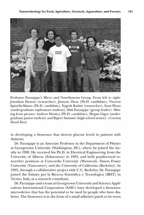
P1: 000
GGBD159C07 GR3880/Mongillo Top Margin: 5/8in Gutter Margin: 3/4in September 25, 2007 16:5
Nanotechnology for Food, Agriculture, Livestock, Aquaculture, and Forestry 161
Professor Paranjape’s Micro and NanoSystems Group. From left to right:Jonathan Hesson (researcher), Jianyun Zhou (Ph.D. candidate), VincentSpinella-Mamo (Ph.D. candidate), Yogesh Kashte (researcher), Sean Flynn(undergraduate sophomore student), Mak Paranjape (group leader). Miss-ing from picture: Andrew Monica (Ph.D. candidate), Megan Giger (under-graduate junior student) and Rajeev Samtani (high school senior). (CourtesyRussel Ross)
in developing a biosensor that detects glucose levels in patients withdiabetes.
Dr. Paranjape is an Associate Professor in the Department of Physicsat Georgetown University (Washington, DC), where he joined the fac-ulty in 1998. He received his Ph.D. in Electrical Engineering from theUniversity of Alberta (Edmonton) in 1993, and held postdoctoral re-searcher positions at Concordia University (Montreal), Simon FraserUniversity (Vancouver), and the University of California (Berkeley). In1995, through a collaborative project with U.C. Berkeley, Dr. Paranjapejoined the Istituto per la Ricerca Scientifica e Tecnologica (IRST) inTrento, Italy, as a research consultant.
Dr. Paranjape and a team at Georgetown University and Science Appli-cations International Corporation (SAIC) have developed a biosensormicro-device that has the potential to be used by people who have dia-betes. The biosensor is in the form of a small adhesive patch to be worn

P1: 000
GGBD159C07 GR3880/Mongillo Top Margin: 5/8in Gutter Margin: 3/4in September 25, 2007 16:5
162 Nanotechnology 101
on the skin and is very convenient to use and makes measuring glucoselevels completely pain-free and in a minimally invasive manner. The mul-tidisciplinary project was funded for over 3 years with technical expertisecoming from several scientific backgrounds: one other physics profes-sor, one professor in pharmacology, two senior researchers from SAIC(biochemistry and engineering), six postdoctoral researchers (chem-istry, materials engineering, biochemistry, microfabrication specialists,and two electrical engineers), and several undergraduate and graduatestudents in the physics program.
Where did you grow up and what were some of your favorite activitiesand subjects as a teenager?I was born in England but I grew up in Canada and lived as a teenager ina small town called Thunder Bay, which is right on Lake Superior, almost30 miles from the United States border north of Minnesota. I enjoyedracquet sports, skiing, and playing hockey—my favorite position wasplaying goal.
What colleges did you attend and what was your major?I completed my undergraduate and graduate degrees, including myPh.D., all in electrical engineering, at the University of Alberta in Ed-monton, Canada. It was during this time when Wayne Gretzky, one of myhockey idols, was playing for the Edmonton Oilers, a National HockeyLeague team that won several back-to-back Stanley Cups while I was inschool.
Presently, what subjects do you teach at Georgetown University?I have an electrical engineering degree, so I teach related subjects suchas electricity and magnetism, and electronics to both physics undergrad-uates and graduate students.
What interested you to become a physics professor, and how did youcross over and get interested in the field of diabetes and in being on ateam that developed a new biosensor device for glucose monitoring?My early interests were to follow in my dad’s footsteps. He is a physicistby training. I also thought about medicine, as well. I liked math a lot andenjoyed hands-on work, but my high school biology skills were not thatgreat. So I wanted to go into physics, but my dad said there are not thatmany jobs (or money) in this field. He thought that since I was math-oriented and a hands-on type person, I should consider engineering. Sothat is how I ended up in electrical engineering.

P1: 000
GGBD159C07 GR3880/Mongillo Top Margin: 5/8in Gutter Margin: 3/4in September 25, 2007 16:5
Nanotechnology for Food, Agriculture, Livestock, Aquaculture, and Forestry 163
How did you get involved in biosensors?The last time I took a biology course was in the 12th grade and I havenot taken any biology courses since then.
After I finished my Ph. D., I started to dabble in biology and biosen-sors during a time when I was employed as a postdoctoral researcherat Simon Fraser University. During this time, while I was involved in aproject to accurately measure the mass of individual cells, such as babyhamster kidney cells, using a relatively new emerging technology calledbiological microelectromechanical systems (or bio-MEMS), I becamevery interested in fabricating devices using microtechnologies, whetherthey are sensors or “machines” that could interact with biological cells.This work was very intriguing to me. Anyway, this is how I got into biosen-sors. I got involved with the glucose-monitoring project soon after arriv-ing at Georgetown University in 1998. Our research team was alreadyinvolved in fabricating noninvasive microdevices for health applications,and after winning a U.S. Defense Department contract for monitoringglucose and lactate in a soldier, the minimally-invasive glucose patch wasdeveloped.
What is the conventional way a person living with diabetes uses tomeasure and monitor his or her glucose level? Approximately, howmany times a day does a person have to do this routine?Typically a person with diabetes, and depending on the severity of thedisease, should sample his or her glucose level at least twice a day. Andthat is the minimum. Typically it is done 3 to 5 times a day—oncewhen you get up, once after breakfast, once after lunch, and once afterdinner, and finally once before bedtime. The more often you monitoryour readings, the better control you have on the disease. However, themore you monitor, the more painful the process can be for many peoplewith diabetes. Remember you are sticking a needle in your finger to drawblood and there is always going to be pain associated with this approach.And one of the big issues related to diabetes control is that many people,because of the pain, will not sample themselves the number of times theyshould in order to control their diabetes. Then after getting a bloodsample, and depending on the glucose reading, a person would injectinsulin, if needed. And this can occur after each glucose reading.
How does the new biosensor device work without puncturing the skinand what are the benefits of the device for patients?For the past few years, the team has been developing and testing a newbiosensor device for glucose monitoring. The size of a small band-aid,it is designed to be worn anywhere on the body, where the biosensor

P1: 000
GGBD159C07 GR3880/Mongillo Top Margin: 5/8in Gutter Margin: 3/4in September 25, 2007 16:5
164 Nanotechnology 101
samples tiny amounts of fluids that lie just beneath the top layer ofskin.
The device is small and convenient, and makes measuring glucoselevels pain-free and minimally invasive.
The biosensor device works to painlessly remove the outer dermis,or dead-skin layer, by using a “micro-hotplate.” The hotplate temper-ature is carefully controlled to apply a small amount of power. The“hotplate” is turned on to a temperature of 130oC. This sounds hot,but in such a small spot the size of a hair follicle, and for such ashort time, a person cannot even detect the heat, or feel any pain,as it is applied to the very outer layers of skin. The biosensor thendetermines the glucose levels from the sample of fluid, which rises tothe skin surface through the micro-pores created by the hotplate, us-ing tiny micro-electrodes that have been coated with a substance thatreacts specifically to the glucose. The fluid being sampled is intersti-tial fluid and not blood, which is commonly used to monitor glucoselevels.
Can young people who are 12 years old or younger use the biosensordevice? Are there any age limits?Any age group can use the biosensor. The ultimate goal of the deviceis not just to monitor the glucose level but eventually, to take stepsto actually inject insulin. The biosensor will form a complete closedloop system so the device will effectively monitor glucose levels anddeliver any insulin if needed. In a sense the envisioned device wouldperform as both biosensor and drug delivery system for the person withdiabetes.
How long does the present biosensor patch last on the body?The present patch contains several sensing sites and each of these sitesprovides a one-time glucose reading. When you are out of sensing sites,then the patch is removed. And this depends on how many times youare sensing your glucose level. The patch, when marketed, could last forabout two weeks depending on the person who will test their glucoselevels say 2 to 3 times a day. However, if you were able to add more andmore sensing sites, then a patch could last much longer.
Is the biosensor device still being tested, and if so, when do you thinkthe device would be available people with diabetes?Usually there is a long process needed for FDA approval of any new drugor new medical devices. However, the patch has some advantages in thatit is a minimally invasive patch because you do not need to implant it

P1: 000
GGBD159C07 GR3880/Mongillo Top Margin: 5/8in Gutter Margin: 3/4in September 25, 2007 16:5
Nanotechnology for Food, Agriculture, Livestock, Aquaculture, and Forestry 165
and you do not need to have to collect blood. Typically these kinds ofdevices are fast-tracked through FDA approval. Once the devices havebeen fully tested using animals, and then after performing clinical trialson human subjects, you can apply for FDA approval. It will take about2 years more for testing on humans. And then the fast track will takeabout 1 to 2 years for FDA approval.
What are some other possible applications for the biosensor device?Let me start by saying this project was sponsored by the Department ofDefense, DARPA (Defense Advanced Research Projects Agency). Theywere interested in using a patch technology, similar to our designedbiosensor patch. The patch would be for the war fighter on the battle-field who could succumb to trauma due to huge losses of blood. Bloodlost is critical so you need to minimize the blood lost as quickly as you canto have a chance of saving the injured trooper. In this application, troopswould be sent onto a battlefield, fitted with a biosensor patch placed ontheir arms. The patch would not hinder them from continuing theirduties.
If injured, the patch would record data about the severity of thetrooper’s wounds based on their glucose and lactate levels (and any otherreadily available bio-molecule that can be sampled with our patch). Thedata would be sent by short-range telemetry to a medic’s palm pilot,for example. The palm pilot would show the location of the injuredtrooper. The severity of the injury would also be ascertained. If themedic observed dangerous changes in a soldier’s body biochemistry,that soldier would be assisted first, and then removed from the fieldfor medical care. So in our continued research, we incorporated themilitary application with the civilian application kept in mind—that is,detecting glucose in people with diabetes.
Do you see other uses of this kind of biosensor?There is a whole list of applications. One other area of interest isto detect, in newborns, the potential of jaundice before its onset.The new mother and baby would leave the hospital and a biosensorpatch would be placed on the child’s arm. If any signs of jaundicewould appear when the child is at home, the patch, which monitorsa biomolecule called bilirubin, would signal an alert. In this way, youwould catch the jaundice earlier and then proceed with medical care.The patch would perform the sensing without pain, unlike current meth-ods that involve inserting a heel stick to draw blood from the newborn’sheel.

P1: 000
GGBD159C07 GR3880/Mongillo Top Margin: 5/8in Gutter Margin: 3/4in September 25, 2007 16:5
166 Nanotechnology 101
What advice would you give young people who would like a career inbiomedical research developing biosensors and other microdevices fordiagnostics?In high school, there is not much overlapping of subjects between thevarious science disciplines. However, at the college level, and in thereal world, there is a lot of interaction and collaboration that takesplace between people who have various backgrounds in physics, chem-istry, biology, mathematics, and engineering. You do not need to bean expert in everything. You can have your own expertise in one sub-ject but always consult others in different fields to see what else can bedone.
You can watch a short film of Prof. Paranjape and the GAEL lab wherethe biosensor device is produced. The film is called, Monitoring BloodGlucose Without Pain or Blood. The Web site is: http://college.georgetown.edu/research/molecules/14887.html
NANO ACTIVITY: FOOD PACKAGING
Since nanotechnology will be applied to the manufacturing of foodpackages you may be interested in learning more about food packag-ing by doing activities from The NSF-funded Materials World ModulesMWM) Program. One of the interdisciplinary modules is called FoodPackaging. In the Food Packaging module, you can learn about the manyfunctions of food packaging and how these materials affect the environ-ment. You can design your own environmentally friendly package fordelivering a hot baked potato and its topping.
See the video of one teacher’s experience in using the modules athttp://www.materialsworldmodules.org/videocenter/MWMinterviewkh.htm
For more information, contact: Materials World Modules, Northwest-ern University, 2220 Campus Drive, Cook Hall, Room 2078, Evanston,IL 60208 or [email protected]
READING MATERIALS
Goodsell, D.S. BioNanotechnology: Lessons from Nature. Hoboken, NJ: Wiley-Liss, Inc.,2004.
Gross, Michael. Travels to the Nanoworld: Miniature Machinery in Nature and Technology.New York: Perseus Books Group, 2001.
Mulhall, Douglas. Our Molecular Future: How Nanotechnology, Robotics, Genetics, andArtificial Intelligence will Transform Our World. Amherst, NY: Prometheus Books,2002.

P1: 000
GGBD159C07 GR3880/Mongillo Top Margin: 5/8in Gutter Margin: 3/4in September 25, 2007 16:5
Nanotechnology for Food, Agriculture, Livestock, Aquaculture, and Forestry 167
National Research Council. Frontiers in Agricultural Research: Food, Health, Environmentand Communities, Committee on Opportunities in Agriculture, Washington, DC:National Academies Press, 2003.
Schnoor, J.L. (Editor). Fate of Pesticides and Chemicals in the Environment (Environ-mental Science and Technology), New York: John Wiley & Sons, 1991.
The United States Department of Agriculture. National Planning Workshop.Nanoscale Science and Engineering for Agriculture and Food Systems. Washington,DC: 2003.
VIDEOS
Monitoring Blood Glucose without Pain or Blood. Go to: http://college.georgetown.edu/research/molecules/14887.html
Detecting Deadly Chemicals. Science Daily. Investigators on a crime scene can nowuse a new tool for collecting chemical or biological samples. The sampler gun collectssamples on a cotton pad—eliminating direct contact with anything harmful, as wellas risk of contaminating evidence—a GPS system to record the samples’ location,a camera that snaps pictures for evidence, and a digital voice recorder and writingpad for taking notes. http://www.sciencedaily.com/videos/2006-12-10/
Detecting Toxics. A new portable lab that detects deadly chemicals in the air. Sci-enceDaily. http://www.sciencedaily.com/videos/2006-02-09/
Materials World Modules. Northwestern University. The NSF-funded MaterialsWorld Modules MWM) Program has produced a series of interdisciplinary mod-ules based on topics in materials science, including Composites, Ceramics, Concrete,Biosensors, Biodegradable Materials, Smart Sensors, Polymers, Food Packaging, andSports Materials. The following video describes the experiences of one teacher whoused the Materials World Modules. Inside MWM: An Interview with Lake Forest Sci-ence Teacher Kate Heroux. In this interview with science teacher Kate Heroux, Pro-fessor Robert Chang, the developer of MWM, discusses the successes and challengesof implementing the Materials World Modules in high school. To see the video goto: http://www.materialsworldmodules.org/videocenter/MWMinterview kh.htm
WEB SITES
Task Force on Building a Science Roadmap for Agriculture, National Associationof State Universities and Land-Grant Colleges (NASULGC), Experiment StationCommittee on Organization and Policy (ESCOP), “A Science Roadmap for theFuture.” November 2001. www.nasulgc.org/comm food.htm
Nanotechnology for the Forest Products Industry—Vision and TechnologyRoadmap. www.fpl.fs.fed.us/highlighted-
National Science and Technology Council. The National Nanotechnology Initiative:Leading to the Next Industrial Revolution, Committee on Technology (InteragencyWorking Group on Nanoscience, Engineering and Technology, Washington, DC:2000. www.ostp.gov/NSTC/html/iwgn/iwgn.fy01budsuppl/toc.htm
United States Department of Agriculture: http://www.usda.gov
U.S. Forest Service: http://www.fs.fed.us

P1: 000
GGBD159C07 GR3880/Mongillo Top Margin: 5/8in Gutter Margin: 3/4in September 25, 2007 16:5
168 Nanotechnology 101
SOMETHING TO DO
Soil Uses
Each state in the United States has selected a state soil, 20 of which have beenlegislatively established. Soils, because of their chemical and physical propertiesdetermine land use purposes, such as farming, mining, and ranching and evenhousing. For a science report, you may want to research and write about your state’ssoil and how the land is used for agriculture and other uses. You can write abouttopics that include soil quality, soil risks and hazards, and soil salinity and planttolerance and how nanotechnology can impact these soil issues. To get informationabout your state soil go to: http://soils.usda.gov/gallery/state soils/

P1: 000
GGBD159C08 GR3880/Mongillo Top Margin: 5/8in Gutter Margin: 3/4in September 25, 2007 16:6
8
Nanotechnology fora SustainableEnvironment
We have learned from the previous chapters that applications of nan-otechnology have the potential to change and improve everything frommedical care and food safety to consumer products and electronics.In addition to these benefits, nanotechnology may help build a moresustainable environment by providing clean drinking water, better airquality, new sources of energies, and a reduction in hazardous and toxicwastes.
WATER POLLUTION AND NANOTECHNOLOGY
By 2015, approximately 3 billion people will live in countries whereit will be difficult to get enough water for basic needs. More than
� Safer Water Worldwide. Industrial toxicolo-gists developed a water purifier which sep-arates particles and organisms from wa-ter and can be used to detect pesticidesin water. Go to Web site. http://www.sciencedaily.com/videos/2006-12-06/
1 billion people will lack ac-cess to clean drinking wa-ter, while others will diefrom contaminated water.The Environmental Protec-tion Agency (EPA) estimatesthat at least 500,000 cases ofillnesses annually can be at-tributed to contaminated drinking water in the United States.
Water can be polluted by excessive amounts of chemicals such as:
Did you know?Heavy metals include metallic elements such asmercury, lead, and arsenic that are hazardous andtoxic and are a health risk for humans and otherliving organisms.
heavy metals, organic chem-icals, disease-causing micro-organisms, sediments, heator thermal pollution andothers. These sources of pol-lutants come from homes,mining activities, municipal sewage plants, industry and manufacturingplants, ranching, and agricultural operations.

P1: 000
GGBD159C08 GR3880/Mongillo Top Margin: 5/8in Gutter Margin: 3/4in September 25, 2007 16:6
170 Nanotechnology 101
NANOTECHNOLOGY AND SAFER DRINKING WATER
Arsenic contamination, both naturally occurring and resulting fromhuman activities, in drinking water is a global problem. For one example,in India, millions of people suffer from arsenic poisoning found indrinking water.
Cleaning Up Arsenic
Scientists are now developing strategies to clean up the arsenic, acarcinogen, in the water. Scientists at Rice University’s Center for Bi-ological and Environmental Nanotechnology (CBEN) have developeda low-cost technology for cleaning arsenic from drinking water. Thetechnology holds promise for millions of people not only in Indiabut also in Bangladesh and in other developing countries where thou-sands of cases of arsenic poisoning are linked to poisoned wells eachyear.
The scientists discovered that nanoparticles of iron oxide (rust) couldbe used to remove arsenic in water by using a magnetic field. Arsenic
Did you know?The following analogy will illustrate how little ofEarth’s freshwater is available: If all of Earth’s watercould fill a 4 liter (about 1 gallon) container, theamount of available fresh water would fill less thana tablespoon out of the 4 liters. As you can see,only a small percentage of freshwater on Earth isavailable for human use.
adheres to rust, according tothe scientists. Rust is essen-tially iron oxide, a combi-nation of iron and oxygen,and tends to be magnetic.The arsenic particles thatstick onto the iron oxide canbe removed from the waterby using a low-powered mag-
net that attracts the particles. Once the particles are extracted, the waterbecomes safe to drink.
The Element Arsenic
The element arsenic is a steel grey metal-like material. Arsenic isa natural part of our environment and widely distributed in Earth’scrust. So living organisms are often exposed to some amount of it.Very low levels of it are always present in soil, water, food, and air.Most arsenic compounds have no smell or special taste, even whenpresent in drinking water. Arsenic has been used in pesticides, poi-sons, chicken-feed supplements, and wood preservatives. However, thenaturally occurring arsenic in the soil can make the water toxic tohumans.

P1: 000
GGBD159C08 GR3880/Mongillo Top Margin: 5/8in Gutter Margin: 3/4in September 25, 2007 16:6
Nanotechnology for a Sustainable Environment 171
Table 8.1 Water Pollutants
Point Sources Bacteria Nutrients
TotalDissolvedAmmonia Solids Acids Toxics
Municipalsewagetreatmentplants
• • • •
Industrialfacilities
• •
Combinedseweroverflows
• • • •
NonpointSources
Agriculturalrunoff
• • • •
Urban runoff • • • •Constructionrunoff
• •
Miningrunoff
• • •
Septicsystems
• • •
Landfill spills •Forestryrunoff
• •
Source: U.S. Environmental Protection Agency.
Nanotechnology and Water Filters
Several companies are developing nanotechnology-based filters thatwill clean polluted water. The filters in the treatment system can sift outbacteria, viruses, heavy metals, and organic material.

P1: 000
GGBD159C08 GR3880/Mongillo Top Margin: 5/8in Gutter Margin: 3/4in September 25, 2007 16:6
172 Nanotechnology 101
One filter product consists of spiral-wound layers of fiberglass sheets.The sheets create a permeable surface of nano-sized pores—a bit-like ananoscale strainer. When pressure is exerted, the water pushes throughthe pores keeping out viruses and bacteria that are too large to gothrough the pores.
In Australia, one company has patented a water treatment technologythat uses nanoparticles for water purification. The product called Meso-Lite has been tested in several countries. The treatment can be used toremove ammonia from contaminated wastewaters. Once the ammoniahas been extracted in the treatment stage, the leftover ammonia can berecycled and used as a commercial fertilizer. The MesoLite process canalso be used as a backup system to support large wastewater treatmentplants.
DRINKING WATER FROM THE OCEAN
The need for a sustainable, affordable supply of clean water is a keypriority for the United States’ future and especially for states that havefew freshwater sources and a fast-growing population. One source ofproviding more fresh water to ocean-side states is to transform unusablewater from the ocean into valuable freshwater. Desalination is the pro-cess that is used for removing dissolved salts from seawater and brackishwater.
Reverse Osmosis
In a water desalination treatment system, reverse osmosis is a separa-tion process that uses pressure to force a solvent, such as water, througha membrane that retains the solute, such as salt ions, on one side andallows pure water to pass to the other side. However, reverse osmosistreatment units use a lot of water and energy and therefore can becostly to operate. As an example, some reverse osmosis treatment plantsrecover only 5 to 15 percent of pure water entering the system. Theremainder is discharged as wastewater. One nanotechnology group mayhave a way to reduce costs of conventional desalination treatments byusing carbon nanotubes.
A New Kind of Reverse Osmosis
Researchers at Lawrence Livermore National Laboratory (LLNL) aredeveloping a water desalination system using carbon nanotube-basedmembranes. The use of the carbon nanotubes in the membranes couldreduce the cost of desalination by 75 percent, compared to reverseosmosis methods used today.

P1: 000
GGBD159C08 GR3880/Mongillo Top Margin: 5/8in Gutter Margin: 3/4in September 25, 2007 16:6
Nanotechnology for a Sustainable Environment 173
The carbon nanotubes used by the researchers are sheets of carbonatoms rolled so tightly that only seven water molecules can fit acrosstheir diameter. Their small size makes them a good source for separatingmolecules. The nanopores also reduce the amount of pressure neededto force water through the membrane As a result, there are savingsin energy costs when compared to reverse osmosis using conventionalmembranes.
Water Pollution: Using the Atomic Force Microscope toStudy Water Pollution
Virginia Tech researchers are using an atomic force microscopy(AFM) to observe how a bacterium adheres to the silica surfaces ofsoil. This sticking efficiency of bacteria has not been previously mea-sured experimentally using the AFM. The researchers believe if theycan learn how bacteria can adhere or stick on to various soil surfaces,then they can use the information to predict how bacteria in the soilparticles can be removed and transported in the groundwater.
GROUNDWATER POLLUTANTS
In the United States, approximately 50 percent of the people dependon underground water naturally stored in aquifers. Surface water pro-vides the other source of fresh water. In fact, many of the rural areas ofthe United States depend almost entirely on groundwater. But some ofthe nation’s groundwater is contaminated, say scientists, and clean upcould cost hundreds of billions of dollars as well as several decades tocomplete.
Groundwater occurs beneath Earth’s surface at depths of a few cen-timeters to more than 300 meters (900 feet). The water that is availablefor human use by pumping operations is within the zone of saturation.The zone of saturation is where the spaces between particles of soil orspaces within fractures of rock that compose the aquifer are entirelyfilled with groundwater. Groundwater concerns include the leaching ofpollutants such as arsenic and MTBE (a gasoline additive, now banned)into the water making it unfit for human consumption. The leachingof buried toxic and hazardous wastes can also pollute groundwater re-sources.
GROUNDWATER CLEANUP
Scientists are developing different technologies for cleaning up pol-lutants in groundwater.

P1: 000
GGBD159C08 GR3880/Mongillo Top Margin: 5/8in Gutter Margin: 3/4in September 25, 2007 16:6
174 Nanotechnology 101
Figure 8.1 Contaminant remediation using permeable reactive barriers.The Permeable Reactive Barriers (PRBs), commonly called “iron walls,” isanother approach to remediate contaminated groundwater. In this process,macro-sized iron particles are placed into the ground forming a perme-able iron barrier or wall that dissolves the pollutants in the groundwater.(Courtesy of Jeff Dixon. Redrawn with permission from Robert M. Powell, HorizonEnvironmental Corporation)
Iron Nanoparticles May Be Effective in Cleaning Up Waste Sites
Professor Zhang of Lehigh University has been working for sev-eral years to develop a remediation method to clean up ground-water contaminants, using nanoscale metallic particles. He has beenfield-testing the method at several industrial sites. The industrial sitesare contaminated with such toxicants as polychlorinated biphenyls(PCBs), DDT (a potent pesticide), and dioxin. These are all chlori-nated hydrocarbons and persistent organic pollutants of types that arefairly insoluble in water; they are found mostly in soil sediments, andfatty animal tissue. So far, the results of his research have been veryencouraging.
Professor Zwang’s technology involves pumping nanoparticles (iron-based particles measuring 100 to 200 nm) into the contaminatedgroundwater. The nanoparticles are almost all iron with less than 1 per-cent palladium. Palladium (Pd) is a rare silver-white metal and is used asa catalyst in catalytic converters on cars. When the iron-based nanopar-ticles are applied to water or soil contaminated with carcinogenicchlorinated solvents, the particles remove the chlorine and convert the

P1: 000
GGBD159C08 GR3880/Mongillo Top Margin: 5/8in Gutter Margin: 3/4in September 25, 2007 16:6
Nanotechnology for a Sustainable Environment 175
solvents into harmless hydrocarbons and chloride, commonly found intable salt.
Professor Zhang’s nanoremediation offers potential advantages overexisting conventional methods. One of the advantages is that nanore-mediation avoids digging up the contaminated soil and treating it—thisis a very costly treatment process.
CLEANING UP ORGANIC POLLUTANTS USINGNANOTECHNOLOGY
Trichloroethene or TCE is one of the most common and poisonousorganic pollutants in U.S. groundwater and one of the nation’s mostpervasive and troublesome groundwater pollutants. TCE is an industrialsolvent used primarily in metal degreasing and cleaning operations.
TCE is found at 60 percent of the contaminated waste sites on theSuperfund National Priorities List, and it is considered one of the mosthazardous chemicals at these sites because of its prevalence and its tox-icity. Superfund is the common name for the Comprehensive Environ-mental Response, Compensation and Liability Act (CERCLA) of 1980.This is a federal law whose mission is to clean up the worst hazardous andtoxic waste site areas on land and water. These sites constitute threats tohuman health and the environment.
TCE, as a volatile organic compound (VOC), has a tendency tovolatilize or escape from groundwater into the air. When this processof volatilization happens in groundwater beneath a building, the TCEcan enter the building as a vapor, which can produce an air quality orinhalation hazard to people within the building.
TCE can be absorbed through the lungs, mucous membranes, gas-trointestinal tract, and the skin. Exposure to TCE happens mostly frombreathing contaminated air and drinking contaminated water. Short-term exposure to high levels of this chemical can result in toxic effectson a number of organs and systems, including the liver, kidney, blood,skin, immune system, reproductive system, nervous system, and cardio-vascular system. In humans, acute inhalation exposure to TCE causescentral nervous system symptoms such as headache, dizziness, nausea,and unconsciousness. TCE has been linked to liver damage, impairedpregnancies, and cancer.
TCE Cleanup with Gold Nanoparticles
Cost is the major hurdle to cleaning up TCE-polluted groundwater.Cleanup costs for TCE nationwide are estimated in the billions of dollars.

P1: 000
GGBD159C08 GR3880/Mongillo Top Margin: 5/8in Gutter Margin: 3/4in September 25, 2007 16:6
176 Nanotechnology 101
The Department of Defense alone estimates the cost of bringing its1,400 TCE-contaminated sites into Environmental PA compliance atmore than $5 billion.
Researchers at Rice University and Georgia Institute of Technologyhave found that gold nanoparticles coated with palladium are extremelyeffective catalysts for breaking down toxic chemicals such as TCE intoless harmful products. Using a treatment of gold nanoparticles, theresearchers hope to drive down the costs of cleanup operations byeliminating:
� the drilling costs for new wells,� the construction costs for surface treatment facilities, and� the energy costs of pumping up water to the surface.
Tests have found that the gold-palladium nanocatalysts break TCEdown about 100 times faster than bulk palladium catalysts. One of themajor advantages of using palladium catalysts to break down TCE isthat palladium converts TCE directly into nontoxic ethene and ethane,colorless, odorless, and gaseous hydrocarbons.
The researchers have another idea and that is to develop a devicethat would include a cylindrical pump containing a catalytic membraneof the gold-palladium nanoparticles. The device would be placed downexisting wells where it would pump water through continuously breakingthe TCE into nontoxic components.
CLEANING UP NUCLEAR WASTE SITES
Scientists believe that using gold-palladium nanoparticles may havean impact on other toxic waste sites, such as the Hanford Nuclear WasteSite located in the southeastern part of Washington State. The site,near the Columbia River, contains nuclear waste material since the endof World War II. Many environmental activists are concerned that thewaste will get into the groundwater. So, maybe a new kind of treatmentmethod using nanoparticles could play a role in preventing the spreadof the nuclear wastes into the groundwater.
AIR POLLUTION
Air pollution is a major health problem in the United States andthroughout the world. An estimated 3 million people die each yearfrom the effects of air pollutants. Medical researchers have linked highlevels of air pollution to illnesses and diseases. These health problems

P1: 000
GGBD159C08 GR3880/Mongillo Top Margin: 5/8in Gutter Margin: 3/4in September 25, 2007 16:6
Nanotechnology for a Sustainable Environment 177
Table 8.2 Applications of Titanium Oxide (TiO2) as a Photocatalyst
� Self-cleaning and bacterial degradation for glass products and forfloors and walls in hospitals.
� Water cleaning capacity and for purification of soil.� Air cleaning effects for pavement blocks and sidewalks.
include asthma, allergies, emphysema, chronic bronchitis, lung cancer,and heart attacks. Pollutants in the air cost citizens billions of dollarsevery year in health care and lost time at work. In a major health studyconducted by the American Lung Association, about 50 percent of theUnited States population is breathing unhealthy amounts of air pollu-tion. Other countries suffer from air pollution too.
Titanium Dioxide and Clean Air
Walking down a street in central London, a person may suddenly feelthat the air quality is quite clean. The sidewalk has been treated witha nanotechnology product containing catalytic properties that breakdown molecules in harmful pollutant emissions in the air. In Milan(Italy) and Paris (France), there are similar concrete sidewalks that aretreated with titanium dioxide (TiO2). According to some experts, thetitanium dioxide concrete slabs have reduced pollutants during rushhour by 60 to 70 percent in these two cities.
Japan’s Mitsubishi Materials Corporation has developed a pavingstone that uses the catalytic properties of TiO2 to remove nitrogenoxides (NOx) from the air. Nitrogen oxides are emitted into the airprimarily from the emissions of automobiles and power plants that burnpetroleum and coal. The paving stone breaks down nitrogen oxides intomore environmental-friendly substances such as nitric acid ions. Theseions can then be washed away by rainfall or neutralized by the alkalinecomposition of the concrete.
What Is Titanium Dioxide?
Titanium dioxide is a white powder. It is used as a whitener for paints,in food products, toothpaste, and many other consumer goods. Tita-nium dioxide is a strong photocatalyst. A photocatalyst produces surfaceoxidation to eliminate bacteria and other materials when it is exposedto the sun or a fluorescent lamp. Therefore, when a product is madeof TiO2 in the sun, organic compounds such as dirt, mold and mildew,and bacteria break down, without consuming the TiO2

P1: 000
GGBD159C08 GR3880/Mongillo Top Margin: 5/8in Gutter Margin: 3/4in September 25, 2007 16:6
178 Nanotechnology 101
Another advantage of products made from titanium dioxide is thatit has a self-cleaning surface. When water hits the titanium dioxide, asmooth sheet forms instead of tiny droplets. The sheet of water getsunder the dirt and lifts it off the surface and washes it away. The com-bination of these effects makes TiO2 self-cleaning to a large extent, andit can be applied in microscopically thin coatings to building materials,glass, or even fabrics.
Scientists in Hong Kong are developing dirt-resistant clothing withtitanium dioxide and a Japanese company has manufactured ceramic
Did you know?Not all air pollution occurs outdoors. In fact, in-door air is often even more polluted than the airoutside homes and workplaces. The United StatesEnvironmental Protection Agency (EPA) ScienceAdvisory Board has ranked indoor air pollutionamong the top five environmental risks to publichealth. Many of these indoor air quality hazardsare attributable to VOCs, such as TCE and otherorganic solvents.
tiles using the chemical.The titanium dioxide self-cleaning ceramic tiles, ac-cording to the NationalInstitute of Health’s Envi-ronmental Health Perspec-tives, have achieved a 99.9percent bacterial kill ratewithin one hour for suchstrains as penicillin-resistantStaphylococcus aureus and Es-cherichia coli.
ENVIRONMENTAL PROTECTION AGENCYAND DEPARTMENT OF ENERGY
Two major federal agencies that will be involved in the development,funding, and applications of nanotechnology for environmental pro-grams to conserve and protect resources and to provide new sourcesof energy will be the Environmental Protection Agency (EPA) and theDepartment of Energy (DOE).
Environmental Protection Agency
The Environmental Protection Agency was created in 1970 and wasestablished in response to growing public concern about: unhealthy air,polluted rivers and groundwater, unsafe drinking water, endangeredspecies, and hazardous waste disposal.
The agency’s mission is to “protect public health and to safeguardthe natural environment—air, water, and land—upon which humanlife depends.” Its areas of responsibility include control of air pollu-tion and water pollution, solid waste management, protection of thedrinking water supply, and pesticide regulation. The EPA is aware that
P1: 000
GGBD159C08 GR3880/Mongillo Top Margin: 5/8in Gutter Margin: 3/4in September 25, 2007 16:6
Nanotechnology for a Sustainable Environment 179
nanotechnology is a revolutionary science and engineering approachthat has the potential to have major consequences—positive andnegative—on the environment.
Department of Energy
The Department of Energy’s (DOE) goal is to advance the national,economic, and energy security of the United States. The department’sstrategic goals to achieve the mission are designed to deliver resultsalong strategic themes that include:
� Energy Security: Promoting America’s energy security through reliable,clean, and affordable energy,
� Environmental Responsibility: Protecting the environment by providinga responsible resolution to the environmental legacy of nuclear weaponsproduction.
NANOTECHNOLOGY AND ENERGY SOURCES
In this century, along with renewal energy sources such as wind energy,geothermal energy, and nuclear energy, many companies are focusingon the technology to produce photovoltaic solar cells and hydrogen fuelcells.
Solar Photovoltaic Cell (PV)
A solar photovoltaic cell (PV) is a device that converts solar energyinto electricity in a manner that does not release any pollutants to theenvironment. Today, solar cells are commonly used to power small-sizeditems such as calculators and watches. But solar PVs have a great futurein providing all the electricity needs for rural communities, homes, andbusinesses. The future for solar cell production and their usage is verypromising as a renewable energy resource. However, the technology stillremains expensive when compared to the costs of fossil fuels to produceelectricity.
Solar cells have two major challenges: they cost too much to make (inthe form of energy), and they are not very efficient. Although efficienciesof 30 percent have been achieved, the present-day typical efficienciesfor solar cells is from 15 to 20 percent. However, solar nano researchersbelieve they can make solar cells more efficient.

P1: 000
GGBD159C08 GR3880/Mongillo Top Margin: 5/8in Gutter Margin: 3/4in September 25, 2007 16:6
180 Nanotechnology 101
Quantum Dots for Solar Cells
Much of the sun’s energy is wasted by today’s photovoltaic cells.When solar photons strike a solar cell, they release electrons in the
Figure 8.2 Konarka Technologies de-velops light-activated Power Plastic R©
that is flexible, lightweight, low in costand much more versatile in applica-tion than traditional silicon-basedsolar cells. These new materials aremade from conducting polymers andnano-engineered materials that canbe coated or printed onto a surfacein a process similar to the way photo-graphic film is made. (Courtesy KonarkaTechnologies, Inc.—Power PlasticTM)
semiconductor to produce an electriccurrent. However, when an electron isset free by the photon, it collides oftenwith a nearby atom making it less likelyto set another electron free. So eventhough the sun’s solar photons carryenough energy to release several elec-trons, producing more electricity, theyare limited to one electron per solarphoton. As a result, conventional solarcells operate at 15 to 20 percent effi-ciency using solar energy.
Scientists have been doing a lot of re-search and experiments with quantumdots to make photovoltaic cells moreefficient. Researchers at the NationalRenewable Energy Laboratory (NREL)and the Los Alamos National Laboratoryhave been experimenting with quantumdots as a semiconductor in a solar cell.They have discovered that the use of thequantum dots allows solar energy to re-lease multiple electrons, not just one.This research has the potential to makemajor improvements in the manufactur-ing of photovoltaic cells. The two re-search teams have calculated that a max-imum of solar conversion to electricityto a 42 percent efficiency rate is pos-sible from the conversion of solar en-ergy to electricity. The solar cells couldbe used to make hydrogen directly fromwater for fuel cells. The researchers stillneed more time and research to com-plete their studies.
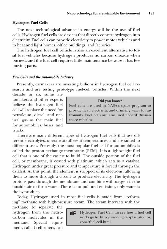
P1: 000
GGBD159C08 GR3880/Mongillo Top Margin: 5/8in Gutter Margin: 3/4in September 25, 2007 16:6
Nanotechnology for a Sustainable Environment 181
Hydrogen Fuel Cells
The next technological advance in energy will be the use of fuelcells. Hydrogen fuel cells are devices that directly convert hydrogen intoelectricity. Fuel cells can provide electricity to power motor vehicles andto heat and light homes, office buildings, and factories.
The hydrogen fuel cell vehicle is also an excellent alternative to fos-sil fuel vehicles because hydrogen produces no carbon dioxide whenburned, and the fuel cell requires little maintenance because it has fewmoving parts.
Fuel Cells and the Automobile Industry
Presently, carmakers are investing billions in hydrogen fuel cell re-search and are testing prototype fuel-cell vehicles. Within the next
Did you know?Fuel cells are used in NASA’s space program toprovide heat, electricity, and drinking water for as-tronauts. Fuel cells are also used aboard Russianspace vehicles.
decade or so, some au-tomakers and other expertsbelieve the hydrogen fuelcell will replace the need forpetroleum, diesel, and nat-ural gas as the main fuelfor automobiles, buses, andtrucks.
There are many different types of hydrogen fuel cells that use dif-ferent electrolytes, operate at different temperatures, and are suited todifferent uses. Presently, the most popular fuel cell for automobiles iscalled the proton exchange membrane (PEM). It is a lightweight fuelcell that is one of the easiest to build. The outside portion of the fuelcell, or membrane, is coated with platinum, which acts as a catalyst.Hydrogen under great pressure and temperature is forced through thecatalyst. At this point, the element is stripped of its electrons, allowingthem to move through a circuit to produce electricity. The hydrogenprotons pass through the membrane and combine with oxygen in theoutside air to form water. There is no polluted emission, only water isthe by-product.
Today, Hydrogen used in most fuel cells is made from “reform-ing” methane with high-pressure steam. The steam interacts with the
� Hydrogen Fuel Cell. To see how a fuel cellworks go to: http://www.digitalsplashstudios.com/fuel-cell.html
methane to separate thehydrogen from the hydro-carbon molecules in themethane. Special equip-ment, called reformers, can

P1: 000
GGBD159C08 GR3880/Mongillo Top Margin: 5/8in Gutter Margin: 3/4in September 25, 2007 16:6
182 Nanotechnology 101
Figure 8.3 Fuel Cell Source. Source: U.S. Department of Energy.
make hydrogen from coal, fossil fuels, nuclear energy, sewage, bacteria,and paper-mill waste. In the future, solar cells may be used to makehydrogen.
The Problem with Fuel Cells
One of the major obstacles in fuel-cell research is designing a safe,lightweight, and compact hydrogen fuel tank that can store sufficientamounts of hydrogen.
Hydrogen is a gas, and is not dense, so to store enough of it in atank you have to compress it at very high pressures. Another option is to
Did you know?The first fuel cell was built in 1839 by Welsh judgeand scientist Sir William Grove. However, the useof fuel cells as a practical generator began in the1960s, when the National Space Administration(NASA) chose fuel cells over nuclear power andsolar energy to power the Gemini and Apollo space-craft. Today, fuel cells provide electricity and wateron the space shuttles.
store the hydrogen gaschemically by bonding itwith another material. Thecarbon nanotubes maybethe answer to the storageproblem. The reason is thathydrogen easily bonds to car-bon nanotubes. Placing agrid of coated nanotubes (orbuckyballs) inside the tank,the nanotubes would “soak

P1: 000
GGBD159C08 GR3880/Mongillo Top Margin: 5/8in Gutter Margin: 3/4in September 25, 2007 16:6
Nanotechnology for a Sustainable Environment 183
up” the hydrogen like a sponge. As a result, the nanotube grid has thecapacity to absorb large amounts of hydrogen gas in a tank about thesize of an automobile gas tank.
Once the tank is filled up with the hydrogen, the driver would startthe car engine. This action would cause the hydrogen to dislodge fromits storage area, the tank, and float through a hose into the fuel cell. Inthe fuel cell, the hydrogen would be converted into electricity and watervapor. However, while fuel cells look promising, more research will needto be done before a mass production of hydrogen fuel cell vehicles areon the road.
EMERGING NANOTECHNOLOGIES AND RISKS
Industry and academic experts suggest there is still uncertainty aboutthe impact of releasing nanoparticles into the environment. It has alsobeen pointed out that there is a lot more to learn about how nanopar-ticles behave when they are released into the environment. Like allemerging technologies with great promise, the nanotechnology andnanochemistry industries will face challenges in ensuring that environ-mental risks are properly managed.
NANO INTERVIEW: PROFESSOR PAUL G. TRATNYEK, Ph.D.,OREGON HEALTH & SCIENCE UNIVERSITY’S OGI SCHOOLOF SCIENCE & ENGINEERING
Professor Paul G. Tratnyek is an environmental chemist and a pro-fessor of environmental and biomolecular systems at Oregon Health &Science University’s OGI School of Science & Engineering, Beaverton,Oregon.
Dr. Tratnyek’s research group, along with collaborators at the PacificNorthwest National Laboratory and the University of Minnesota, hasdiscovered that at least one type of nano-sized particles of iron may behelpful in cleaning up carbon tetrachloride contamination in ground-water. Carbon tetrachloride is a chemical that is used in dry-cleaningapplications and as a degreasing agent to clean tools. Carbon tetrachlo-ride is a toxic chemical that has shown to cause cancer in animals.
The prospect of using iron nanoparticle technology for environmen-tal cleanup is promising. However, Dr. Tratnyek states that there are alot of unanswered questions about the appropriate implementation ofthis technology and even some questions about its safety.
Dr. Tratnyek talked to the author about his career and his environ-mental work in groundwater contamination.

P1: 000
GGBD159C08 GR3880/Mongillo Top Margin: 5/8in Gutter Margin: 3/4in September 25, 2007 16:6
184 Nanotechnology 101
Where did you grow up and what schools did you attend?I grew up in Sudbury, Massachusetts, a suburb of Boston. I wentto the public high school and then to Williams College in Western
Professor Paul G. Tratnyek is an environmen-tal chemist and a professor of environmentaland biomolecular systems at Oregon Health& Science University’s OGI School of Science& Engineering, Beaverton, Oregon. (CourtesyAnne Rybak Photographic)
Massachusetts where I receivedmy bachelor’s degree. AfterWilliams College, I went tothe Colorado School of Minesin Colorado and received myPh.D. degree in applied chem-istry. The reason I selectedthe Colorado School of Minesto study was because I wasinterested in the link betweenchemistry and the earth sci-ences.
What were some of yourfavorite activities and subjectsin school?As a young person in elemen-tary school I was very interestedin the environmental scienceactivities and natural history.Through high school and col-lege I focused mainly on the “ba-sics,” i.e., chemistry, physics, andmathematics. Only in graduateschool did I come back aroundto studying environmental sci-ence.
How did you get interested inusing iron particles in cleaningup contaminants ingroundwater?
When I arrived at the Oregon Graduate Institute and became a professor,one of my senior mentors, another professor in the department, knewthe group in Canada that had first stumbled onto the possibility of usingiron metal to remediate contaminated groundwater. But the group haddifficulty addressing the chemical aspect of that technology. I offered tohelp with that, and they provided a small amount of funding for me toget started. My early results helped explain how the technology worked

P1: 000
GGBD159C08 GR3880/Mongillo Top Margin: 5/8in Gutter Margin: 3/4in September 25, 2007 16:6
Nanotechnology for a Sustainable Environment 185
and this gave people confidence and boosted the commercial viabilityof the technology.
How does groundwater become contaminated?Groundwater contamination occurs all over the place and comes fromtwo forms—point sources and nonpoint sources. Point source meansthat the contamination was discharged to the environment from somelocalized source, such as a dry-cleaning plant or from a factory or busi-ness that had a leaking pipe or had spilled the contaminants. Nonpointsources include contamination that was distributed broadly across a wideenvironment. Pesticides often present nonpoint source contaminationproblems because they are introduced to the environment over largeareas, by aerial spraying, or the like.
Nonpoint and point sources are both big problems and it is difficultat times to know where the source of the contamination came from.What you usually hear in the news is the point source contaminationcases because you can get names of some companies who buried toxicmaterials in their backyards. Many of these are Superfund sites, whichget a lot of press.
What are some of the contaminants found in groundwater and whichones are the most harmful to human health?Overall, the most significant contaminants probably are the chlorinatedsolvents, which were used in dry cleaning, degreasing, cleaning circuitboards in the electronic industry, etc. Big and small spills of these chem-icals are widespread. The chlorinated solvents are toxic (e.g., some arecarcinogenic) and therefore present real problems when they contam-inate groundwater used for drinking purposes. Besides chlorinated sol-vents, there are other major categories of contaminants: gasoline andother fuels; metals like chromate, etc.
What is the most common or traditional method that is used forgroundwater remediation?The most traditional method is referred to as a “pump and treat.” Thisinvolves pumping the groundwater out of the ground and treatmentof the contamination at the surface. Because treatment is done aboveground, it’s called an “ex situ” method.
In this process, a well is put into the ground where there is contami-nated groundwater. A pump is attached to the well and if the pumpingis successful it will draw some of the contamination out of the ground tothe surface. Then the contaminants are treated in a variety of differentways, usually be adsorption to activated carbon filters. The pump and

P1: 000
GGBD159C08 GR3880/Mongillo Top Margin: 5/8in Gutter Margin: 3/4in September 25, 2007 16:6
186 Nanotechnology 101
treat is easy from an engineering standpoint. However, this process isalso criticized as being inefficient for two related reasons. The pumpand treat method tends not to solve the problem, but just controls it.This means that you have to continue to pump these contaminated ar-eas for a long period. If the well pumps are turned off, the contaminantconcentrations tend to rebound.
The constant daily pumping operation is costly. Ex situ process canalso be tied up in legal and regulatory issues because once the contami-nated water is pumped up to the surface you cannot just dump it backon the ground again because it is hazardous waste, so you need to gothrough regulatory and legal requirements to remove it.
You have been studying how iron particles break down pollutants since1992. One technology you and your colleges helped to develop was theuse of Permeable Reactive Barriers (PRBs), commonly called “ironwalls,” to remediate contaminated groundwater. In this process,however, you used macro-sized iron particles. What are iron walls andwhat are the advantages of using this process for cleanup rather thanthe traditional remediation technologies?The “iron wall” or permeable reactive barriers (PRBs) has two maincharacteristics—it is in situ and it is passive. In situ means that youapply iron particles by placing them into the ground and treat thecontamination there. You do not have to pump the contaminated waterup to the surface. The other advantage is that this method is passive.Pump and treat is active because you have to constantly keep the pumpsworking. Ideally passive technologies mean that once the treatment isin place you can cover it up, plant grass, and then you can leave thearea—there is nothing else to do.
Passive can be much less expensive in the long haul than pump andtreat which is an active process. In situ allows you to put iron particlesand materials down into the ground to interact with the groundwa-ter to remove the contaminants. The groundwater will flow throughthis treatment zone and be treated and what comes out at the end iscleaned. The iron wall also serves the function of an in-ground cutoffwall. This means you can intercept the contaminated groundwater in avery precise way—you cut it off. This cutoff wall is useful in many wayswhere many properties are near one another. So, if someone spills toxicmaterials into the ground and contaminates the groundwater, you canuse a cutoff wall to keep the contaminants from entering the ground-water of the nearby neighbor’s property, or discharging into surfacewater.

P1: 000
GGBD159C08 GR3880/Mongillo Top Margin: 5/8in Gutter Margin: 3/4in September 25, 2007 16:6
Nanotechnology for a Sustainable Environment 187
How does iron break down the contaminants?Traditionally iron walls have been made with granular iron particles thatare the size of millimeters. These coarse iron grains are fairly inexpen-sive and plentiful. When contaminated water interacts with the metal,a chemical reaction takes place. The reaction removes the chlorines,which makes the products less toxic. In a traditional iron wall, the ironremains available to degrade contaminants pretty much indefinitely.
Do the iron particles have any advantages over the use of other metalsfor groundwater remediation?You can use other metals but iron is better because it is less harmful tothe environment than other metals. Iron is cheaper too. There are twomethods of using iron particles in groundwater remediation.
The traditional way or the most common way of making permeableiron walls (PRBs) is to use iron particles that are manufactured for theconstruction industry. These micron-sized iron particles are coarse andgranular-shaped.
Recently, however, there has been interest in the PRB field in usingnano-sized iron particles for cleaning up contaminants in groundwater.Nano-sized particles range in size from 10 to 100 nanometers. Much ofthis process is similar to the conventional iron wall method for clean up.However, there are a few differences. The nanoparticles particles are sosmall that you can make slurry solutions and then inject the solutionsinto the wells. By using this process, you can create an iron wall, butat a much greater depth than the conventional PRB way. This is hugeadvantage. The downside is that when you inject the iron nanoparticlesinto the ground, it is not clear how far the particles will move once theyare in the groundwater.
Generally, nanoparticles do not move very far, in fact they do not movefar enough. You want the nanoparticles to move farther. Researchersare working on ways to make nanoparticles go farther, but if they gettoo good at this the particles might move to places we don’t want them(drinking water supplies, for example). So, we need to do more researchto try to figure out if this PRB process poses a potential problem.
Once these “iron walls” are placed in the soil how long is it before theyneed to be replaced?The installation of the conventional non-nano iron wall has lasted forsome time. There are a good number of iron walls that have worked formore than 10 years.
We expect that the nanoparticle iron wall installation will not last verylong, because the nanoparticles are so small that they will be used up in a

P1: 000
GGBD159C08 GR3880/Mongillo Top Margin: 5/8in Gutter Margin: 3/4in September 25, 2007 16:6
188 Nanotechnology 101
short time. Therefore, it is difficult to estimate how long the nanoparticleiron wall will last. Our best estimate is that the nanoparticle iron wallwill probably last only for a few months. The goal of the nanoparticleiron wall is to knock out the contaminants quickly.
Where have these “iron walls” been used in Oregon and elsewhere?The convention iron wall (PRBs) was first used by researchers at theUniversity of Waterloo at a site in Ontario, Canada. In the U.S., thefirst large-scale conventional iron wall was used in an industrial park inSunnyvale, California. Since then, there have been many applications ofthe conventional PRB.
The iron nanoparticle remediation process is much newer and thereare fewer of those that have been implemented. The first pilot programwas initiated by Professor W.X. Zhang at Lehigh University. He estab-lished a pilot program at a chemical manufacturing site on the east coastand reported some favorable results. This was the first pilot-scaled pro-gram and since then there have been a number of consulting companiesthat have done more than a dozen versions of the nanoparticle iron wallinstallations.
Are there any risks in using iron nanoparticles for groundwaterremediation and if so, what would some of these risks be?There is much debate going on about the use of nanoparticles. The riskshave two parts; one is toxicity and the other part is the exposure part.Nanoparticles can be toxic, especially if you inhale them, but will therebe any harm to humans and animals? That depends on whether thereis exposure to these iron nanoparticles.
Different situations pose different risks. If you are in the businessof manufacturing these particles then you have occupational healthissues that you need to worry about. However, once you inject theseparticles into the ground for remediation there is very little chance thatanyone will be exposed to those iron particles. It is quite clear that theseparticles are not very mobile in groundwater because they tend to stickonto anything available for them to attach to. A general rule is onceyou inject these particles into the ground they may move only a few feetfrom where you have injected them. So there is little likelihood that thenanoparticles will show up in the neighbor’s drinking water well that is300 feet away.
I heard that scrap iron is used to make iron particles used forgroundwater remediation. Is this true? If so, how is it used?The conventional commercial granular iron micro-particles (not ironnanoparticles) that are used in a conventional iron wall come from a

P1: 000
GGBD159C08 GR3880/Mongillo Top Margin: 5/8in Gutter Margin: 3/4in September 25, 2007 16:6
Nanotechnology for a Sustainable Environment 189
variety of scrap metal dealers, many from the Midwest. These materi-als come from sources like old brake drums. The scrap iron is shred-ded and then it is cleaned to remove any grease or oil on the metal,and is sold for a variety of commercial applications such as hardeningconcrete.
The iron nanoparticles are not made this way. Iron nanoparticles areusually made in a process called bottom-up nanofabrication. Nanopar-ticles start with a solution of iron and some other materials and thenyou precipitate the nanoparticles out of the solution starting from themolecules going to the nanoparticles.
In one of your articles, you described an experiment forundergraduate general chemistry students. In the experiment, thestudents investigated the chemistry behind the iron-permeable reactivebarriers (iron walls) used to remediate contaminated groundwater. Isthis an activity that high school chemistry students could also performsafely, under supervision, in their science class?Yes, Students and teachers can refer to a 4-page article, A Discovery-Based Experiment Illustrating How Iron Metal is Used to Remediate Contami-nated Groundwater. For the article, go to: http://cgr.ebs.ogi.edu/merl/resources.htm
From reading the article, teachers and students can get enough in-formation to investigate the details of the degradation process in thePRB contaminant system by determining the various parameters for thedegradation of a dye in place of a contaminant. Dyes have often beenused as model contaminants. So, we use a dye in this activity because itis nontoxic and it works well.
In the activity, students measure the kinetics of the disappearance ofa dye solution in a cuvette containing granular iron particles—not theiron nanoparticles. There is a nice illustration in the article that showsthe degradation process of the dye. If you wish, you can also monitorthe dye concentration by using a UV-vis spectrophotometer. We havehad high school teachers who have worked on several variations of thisactivity.
Resources for Educators and Students
1. A multimedia CD-ROM (MERL: Metals for Environmental Remediation andLearning), which provides more details on the history, development, in-stallation, and chemistry of iron walls, is available from the authors. Seehttp://cgr.ebs.ogi.edu/merl/ (accessed on October 2001) for more in-formation.

P1: 000
GGBD159C08 GR3880/Mongillo Top Margin: 5/8in Gutter Margin: 3/4in September 25, 2007 16:6
190 Nanotechnology 101
2. Useful information on iron walls can be found at many Web sites, in-cluding http://cgr.ebs.ogi.edu/iron; http://www.rtdf.org; http://www.doegjpo.com/perm-barr/.
NANO ACTIVITY: DISCOVERING THE PROPERTIES OFFERROFLUIDS (Teacher Supervision Advised)
Nanotechnologists are experimenting with ferrofluids to help cleanup wastewater. Ferrofluids contain nanoparticles of a magnetic solid,usually magnetite (Fe3O4), in a colloidal suspension.
NASA discovered ferrofluids when their scientists were trying to con-trol liquid products in space. Ferrofluids have been used in many ap-plications, including computer disk drives, low-friction seals, and loud-speakers.
In this activity, you will learn about some of the properties of ferroflu-ids. The activity was adapted from the NanoSense Program produced bythe SRI International in Menlo Park, California. Patricia Schank andTina Stanford coauthored the activity. To learn more about this nanoactivity and other NanoSense activities go to: www.nanosense.org (SafetyNote: You should do the following activity with teacher supervision.)
Materials You Need
1. Sealed display cells of ferrofluids (for ordering, see Where to Buy)
2. Magnet
� Have your teacher show and pass around one or more samples of fer-rofluid along with a strong magnet. Under teacher supervision, let stu-dents play with the ferrofluids and magnet and see what they can make itdo. The teacher may also want to show and pass around another magneticmaterial, like a piece of iron, for comparison. The teacher should explainto the students that since we have been able to make the particles in theferrofluids so small, we have been able to change the physical state of thematerial from a solid to a liquid.
� What happens when you bring a magnet close to the liquid?� When you put the magnet near the ferrofluids, it distorts. What causes
this distortion?� What does this distortion represent?
Where to Buy Ferrofluids
The science department or the science teacher can order sealed dis-play cells of ferrofluids from Educational Innovations, Inc., at: http://

P1: 000
GGBD159C08 GR3880/Mongillo Top Margin: 5/8in Gutter Margin: 3/4in September 25, 2007 16:6
Nanotechnology for a Sustainable Environment 191
www.teachersource.com (click on “Browse or Search the Catalog”, “Elec-tricity! Magnetism! Engines!” and then “Ferrofluids”). A Ferrofluid Ex-periment Booklet is also available (item FF-150) for about $6.
References
http://jchemed.chem.wisc.edu/JCESoft/CCA/CCA2/MAIN/FEFLUID/CD2R1.HTM
READING MATERIAL
Karn, Barbara, Vicki Colvin, Paul Alivasatos, Tina Masciangioli (Eds.). Nanotechnologyand the Environment. Washington, DC: American Chemical Society, 2004.
Lewis, Scott Alan. The Sierra Club Guide to Safe Drinking Water. San Francisco: SierraClub Books, 1996.
Roco, Mihail C., and William Sims Bainbridge. Societal Implications of Nanoscience andNanotechnology. Boston, MA: Kluwer Academic Publishers, 2001.
Somerville, Richard C.J. The Forgiving Air: Understanding Environmental Change. Berke-ley, CA: University of California Press, 1998.
Wiesner, Mark, and Jean-Yves Bottero. Environmental Nanotechnology. New York. Mc-Graw Hill Professional Publishing, 2007.
VIDEOS
Photovoltaics. Turning Sunlight into Electricity. United States Department of En-ergy. Solar Energies Technologies Program: Animations. The “photovoltaic ef-fect” is the basic physical process through which a PV cell converts sunlightinto electricity. Sunlight is composed of photons or particles of solar energy.http://www1.eere.energy.gov/solar/video/pv3.mov
Clean Technology Vehicles. Altairnano. Demonstration vehicle using NanoSafe long-term batteries for vehicles. http://www.altairnano.com/ZEV.mov
Hydrogen Fuel Cell. Digital Splash Multimedia Studios. http://www.digitalsplashstudios.com/fuel-cell.html
How a Fuel Cell Works. Ballard Fuel Cells. Ballard’s principal business is the design,development, and manufacture of proton exchange membrane (PEM) fuel cellproducts. (Scroll down)
http://www.ballard.com/be informed/fuel cell technology/how the technologyworks
WEB SITES
National Institute for Occupational Health (NIOSH): http://www.cdc.gov/niosh/homepage.html
Copies of the National Air Quality and Emissions Trends Report are available from U.S.Environmental Protection Agency. Copies of the report may be viewed via the OARWeb site at: http://www.epa.gov/docs/oar/oarhome.html
Environmental Protection Agency: http://www.epa.gov/

P1: 000
GGBD159C08 GR3880/Mongillo Top Margin: 5/8in Gutter Margin: 3/4in September 25, 2007 16:6
192 Nanotechnology 101
A site for innovative technologies for contaminated soil and groundwater.
Department of Energy: http://www.energy.gov/index.htm
National Renewable Energy Laboratory (NREL): www.nrel.gov/
Sandia National Laboratories: http://www.sandia.gov/
SOMETHING TO DO
Do you ever wonder how much energy your school building uses? Could you becomean energy consultant who could design a nanotechnology program to save energy?If you do, you may want to go to the EnergyNet sponsored by the Department ofEnergy. They have several energy projects on their Web site.
Energy Audits
Here is one online project from the Department of Energy that will give you andothers in grades 6–12 the opportunity to act as energy consultants for their schools.In this project, you can conduct energy audits to review the energy use in your schoolor other buildings. For directions go to:
http://www.energynet.net/eninfo/info/what is energynet.html
The U.S. Department of Energy also has a Web site of many other kinds of activitiesto do. Here is their Web site:
http://www1.eere.energy.gov/education/lesson plans.html

P1: 000
GGBD159C09 GR3880/Mongillo Top Margin: 5/8in Gutter Margin: 3/4in September 25, 2007 16:6
9
NanotechnologyProjects and theUnited StatesGovernment
Nanotechnology is expected to have a large impact on many sectorsof the United States and the world’s economy. All governments agreethat a strong nanotechnology economy can lead to new products, newbusinesses, new jobs, and even new industries for many countries. As aresult, nanotechnology funding for research is growing rapidly in manycountries.
The U.S. government is aware of the economic and social impactsthat nanotechnology can make. For several decades, the governmenthas funded nanotechnology research.
NATIONAL NANOTECHNOLOGY INSTITUTE
However, a big push for more government investment in nanotech-nology research occurred in 2001. At that time, President Clinton re-quested in the 2002 federal budget a major new initiative, called theNational Nanotechnology Initiative (NNI). The budget included an in-crease of more than 200 million dollars for the government’s investmentin nanotechnology research and development.
Additional nanotechnology dollars were authorized during PresidentBush’s term. In December 2003, President Bush signed the Nanotech-nology Research and Development Act, which authorizes funding fornanotechnology research and development (R&D) nanotechnology.This legislation puts into law programs and activities supported by theNational Nanotechnology Initiative (NNI). The legislation also autho-rizes public hearings and expert advisory panels, as well as the AmericanNanotechnology Preparedness Center to study the emerging technol-ogy’s potential societal and ethical effects.
According to one report, from 2001 to 2007, NNI participants formedover 60 facilities or institutes involved in nanotechnology research

P1: 000
GGBD159C09 GR3880/Mongillo Top Margin: 5/8in Gutter Margin: 3/4in September 25, 2007 16:6
194 Nanotechnology 101
Table 9.1 United States Government Expenditures in Nanotechnology(in millions of dollars, approximately)
Agencies 2002 2003 2004 2005 2006 2007
NationalScienceFoundation
$ 204 $ 221 $ 256 $ 338 $ 344 $ 373
Department ofDefense
$ 224 $ 322 $ 291 $ 267 $ 436 $ 345
Department ofEnergy
$ 89 $ 134 $ 202 $ 216 $ 207 $ 258
Other FederalAgencies
$ 136 $ 142 $ 183 $ 217 $ 251 $ 259
and development throughout the United States. New centers of nan-otechnology expertise, most of which are associated with universities,train workers and help educate researchers and developers of tech-nology.
Spending on nanotechnology research and development (R&D) hasamounted to several billions of dollars since the late 1990s, by the UnitedStates alone and accounts for a large portion of worldwide spending onthis type of work. The government agencies that have spent the greatestamounts on nanotechnology are the National Science Foundation, theDepartment of Energy, and the Nation Institutes of Health.
In nanotechnology research, engineers, medical doctors, educa-tors, chemists, physicists, nanotechnology researchers usually collabo-rate on studies and projects. Nanotechnology researchers often mustshare equipment, because many of the high-technology microscopesand other devices used in this technology are too expensive for eachindividual research facility to purchase and maintain its own. For ex-ample, acquiring a scanning electron microscope and building a clean-room can cost millions of dollars. So, grants and loans from govern-ment and private institutions provide money for such activities andequipment.
So far, the NNI has already made valuable contributions to the devel-opment of nanotechnology. With NNI funding, researchers have beenworking on gold nanoshells that can target the destruction of malig-nant cancer cells (See Chapter 5), low-cost solar cells and quantum dotsfor energy sources (See Chapter 6), and nanoscale iron particles thatcan reduce the costs of cleaning up contaminated groundwater (SeeChapter 8).

P1: 000
GGBD159C09 GR3880/Mongillo Top Margin: 5/8in Gutter Margin: 3/4in September 25, 2007 16:6
Nanotechnology Projects and the United States Government 195
THE NATIONAL NANOTECHNOLOGY INITIATIVE (NNI) ANDFEDERAL AGENCIES
The main goal of the National Nanotechnology Initiative (NNI) isto coordinate all of the federal agencies’ efforts in nanoscale science,engineering, and technology. Three of these federal agencies were cov-ered in earlier chapters. They included the Department of Agriculturein Chapter 7 and the work of the Environmental Protection Agency andthe Department of Energy in Chapter 8.
This chapter will report on nanotechnology research at the NationalScience Foundation, Department of Defense, National Institute of Stan-dards and Technology, National Institute of Occupational Safety, Depart-ment of Homeland Security, and the National Aeronautics and SpaceAdministration.
NATIONAL AERONAUTICS AND SPACE ADMINISTRATION (NASA)
President Dwight D. Eisenhower established the National Aeronauticsand Space Administration (NASA) in 1958; this was the time of the thenSoviet Union’s launch of the first artificial satellite. NASA grew outof the National Advisory Committee on Aeronautics, which had beenresearching flight technology for more than 40 years. NASA’s missionis to pioneer the future in space exploration, scientific discovery, andaeronautics research.
In Chapter 5, you read a little bit about NASA’s lab-on-a-chip.
Lab-on-a-Chip
According to NASA, the lab-on-a-chip technology can be used for newtools to detect bacteria and life forms on Earth and other planets and
Did you know?Since the lab-on-a-chip is small device, a large num-ber of them could be carried on a Mars rover tosearch for life and for monitoring microbes insideMartian habitats.
for protecting astronauts bymonitoring crew health anddetecting microbes and con-taminants in spacecraft.
On Earth, some basiclab-on-a-chip technology ap-proaches are being used forcommercial and medical diagnostic applications. As an example, the lab-on-a-chip technology can be used as an in-office test for strep throat, ormodern in-home pregnancy tests. The hand-held portable device, con-taining a simple chip design, can conduct diagnostic tests and recordtest results in a short time for the patient.

P1: 000
GGBD159C09 GR3880/Mongillo Top Margin: 5/8in Gutter Margin: 3/4in September 25, 2007 16:6
196 Nanotechnology 101
Lab-on-a-chip. The lab-on-a-chip is a microfabricated device that performschemical and biochemical procedures under computer control, usingminiscule quantities of samples to be analyzed. (Courtesy U.S. Department ofEnergy, Oak Ridge National Laboratory)
Spacecraft
In the near future NASA may use combinations of plastics and othermaterials that will greatly reduce the weight of a spacecraft. Less weightin the spacecraft can reduce launch costs.
Carbon fiber technology has already been used to replace many space-craft components. Presently, the B-2 Stealth Bomber uses carbon fibermaterials in its wings. Carbon fiber composites, for example, are fivetimes stiffer than steel for the same weight allowing for much lighterstructures. In addition, carbon fibers have the highest thermal conduc-tivity; they do not overheat. This property allows the carbon fibers tobe used as heat dissipating elements on the outside of the craft forspacecraft reentry protection.

P1: 000
GGBD159C09 GR3880/Mongillo Top Margin: 5/8in Gutter Margin: 3/4in September 25, 2007 16:6
Nanotechnology Projects and the United States Government 197
A Self-Repair Spacecraft
Using advanced nanotechnology, the spacecraft may adapt to con-ditions in space travel by rebuilding itself, as needed, while inflight. Solar energy from the spacecraft solar panels would powerthe computers and assemblers. This would also allow general re-pair and maintenance to occur without using crew repair astro-nauts.
Spacecraft Recycling
Recycling aboard the spacecraft will be greatly improved by nanotech-nology. Recycling at the atomic level will be very efficient and, in closedenvironments, such as space stations, this will be crucial. Nanotechnol-ogy should also be able to recycle the air efficiently as well, providing ahigh-quality life support system. Recycling water is also well within thecapabilities of nanosystems with all waste molecules being recycled andused elsewhere.
Improvements in NASA Spacesuits
The new nano-designed spacesuits will be light, thin, comfortable,and easy to work with but they will have enhanced strength. The suit willautomatically adjust to the contours of the astronaut’s body when it isput on. The suit will be able to repair itself.
NASA Space Elevator
A space elevator is essentially a long cable extending from the Earth’ssurface to a tower in space. The space elevator will orbit Earth at about36,000 kilometers in altitude.
Four to six “elevator tracks” would extend up the sides of thetower and cable platforms, at different levels. These tracks would allow
Did you know?What will be the first major space commercial busi-nesses? The top two businesses may be passengerflights and mining. Advertising is also a possibility.
electromagnetic vehicles totravel at speeds reachingthousands of kilometers-per-hour. The vehicles travelingalong the cable could serveas a mass transportation sys-tem for moving people, payloads, and power between Earth and space.Security measures are also planned to keep the cable structure fromtumbling to Earth.
Carbon Nanotubes and the Space Elevator. To build such a sky-high el-evator, very strong materials would be needed for the cables (tethers)and the tower. Carbon nanotubes could be the answer for constructing

P1: 000
GGBD159C09 GR3880/Mongillo Top Margin: 5/8in Gutter Margin: 3/4in September 25, 2007 16:6
198 Nanotechnology 101
the cables. Carbon nanotubes appear to have the potential strength thespace elevator needs.
According to NASA researchers, carbon nanotubes are 100 timesstronger than steel. The space elevator will become a realistic possibility
� Space Elevator. Scientists envision a spaceelevator based in the Pacific Ocean. Go to:http://www.sciencentral.com/articles/view.php3?article id=218392162&language=english
with nanotube fibers thatnanotechnology will provide.Maximum stress is at the high-est point—the altitude, so thecable must be thickest thereand taper exponentially as itapproaches Earth. Using this
material, a cable could be constructed, probably downwards from thespace station.
However, NASA states that the space elevator construction is not fea-sible today, but it could be toward the end of the 21st century.
NATIONAL SCIENCE FOUNDATION
The National Science Foundation (NSF) is an independent federalagency. Their goal is to promote the progress of science; to advance thenational health, prosperity, and welfare; to secure the national defense.NSF funds support basic research conducted by America’s colleges anduniversities. About 1,300 projects involving more than 6,000 faculty andstudents are supported each year.
The NSF funds the National Nanofabrication Users Network (NNUN)and the Network for Computational Nanotechnology (NCN). TheNNUN includes five university-based research hubs which are focused onelectronics, biology, advanced materials, optoelectronics, and nanoscalecomputer simulation. The NCN, centered at Purdue University, is link-ing theory and computation to experimental work that helps turn thepromise of nanoscience into new nanotechnologies.
The National Science Foundation funds a number of projects. Oneexample of a funded nanoproject includes nano research work doneat the University of Akron. Scientists at the University of Akron haveshown how to create a densely packed carpet of carbon nanotubes thatfunctions like an artificial gecko foot—but with 200 times the geckofoot’s gripping power. Potential applications include dry adhesives formicroelectronics, information technology, robotics, space, and manyother fields.
Another NSF program that was funded included work at the Uni-versity of Wisconsin-Madison. Researchers were able to begin the pro-cess of developing nanoscale electronic devices that can be directed to

P1: 000
GGBD159C09 GR3880/Mongillo Top Margin: 5/8in Gutter Margin: 3/4in September 25, 2007 16:6
Nanotechnology Projects and the United States Government 199
The National Science Foundation funded an exhibit called “It’s a NanoWorld.” The traveling exhibit, organized by Sciencenter in Ithaca, NewYork, is a hands-on interactive exhibition that introduces children and theirparents to the biological wonders of the nanoworld. At this station in theexhibit, visitors are using magnifying glasses to look at tiny parts of feathers,shells, and seeds. (Courtesy Sciencenter, Ithaca, NY)
self-assemble themselves automatically. This research developmentwould allow manufacturers to mass-produce nanochips having circuitelements only a few molecules across. The mass production of thenanochips would provide large quantities of chips to be developed withpossible lower costs per unit.
National Science Foundation Classroom Resources
The NSF provides Classroom Resources, a diverse collection of lessonsand Web resources for classroom teachers, their students, and students’families. Go to: http://www.nsf.gov/news/classroom/
NATIONAL INSTITUTE OF STANDARDS ANDTECHNOLOGY (NIST)
The National Institute of Standards and Technology (NIST) mission isto promote U.S. innovation and industrial competitiveness by advancingmeasurement science, standards, and technology in ways that enhance

P1: 000
GGBD159C09 GR3880/Mongillo Top Margin: 5/8in Gutter Margin: 3/4in September 25, 2007 16:6
200 Nanotechnology 101
economic security and improve our quality of life. Researchers in NIST’sdevelop measurements, standards, and data crucial to private industry’sdevelopment of products for a nanotechnology market that could reach$1 trillion during the next decade. NIST’s work also aids other federalagencies’ efforts to exploit nanotechnology to further their missions,such as national security and environmental protection.
THE FOOD AND DRUG ADMINISTRATION (FDA)
The Food and Drug Administration (FDA) is an agency of the UnitedStates Department of Health and Human Services and is responsible forregulating
� food,� dietary supplements,� drugs and cosmetics,� biological medical products,� dietary supplements,� color additives in food,� blood products, and� medical devices.
FDAconducts research in several of its Centers to understand the char-acteristics of nanomaterials and nanotechnology processes. Research in-terests include any areas related to the use of nanoproducts that FDAneeds to consider in the regulation of these products. As an exampleof current research, FDA is collaborating with other agencies on studiesthat examine the skin absorption and phototoxicity of nano-sized tita-nium dioxide and zinc oxide preparations used in sunscreens. If anyrisks are identified, which may occur from these nano chemicals used insunscreens, then additional tests or other requirements may be needed.
FDA only regulates certain categories of products. Existing require-ments may be adequate for most nanotechnology products that we willregulate. These products are in the same size-range as the cells andmolecules that FDA reviewers and scientists associate with every day.
DEPARTMENT OF DEFENSE (DOD)
The mission of the Department of Defense is to provide the militaryforces that are needed to deter war and to protect the security of theUnited States. The department’s headquarters is at the Pentagon.

P1: 000
GGBD159C09 GR3880/Mongillo Top Margin: 5/8in Gutter Margin: 3/4in September 25, 2007 16:6
Nanotechnology Projects and the United States Government 201
The DOD has a long history of supporting innovative nanotechnol-ogy research efforts for the future advancement of warfighter and battlesystems capabilities. The DOD includes the Defense Advanced ResearchProjects Agency (DARPA), Office of Naval Research (ONR), Army Re-search Office (ARO), and the Air Force Office of Scientific Research(AFOSR).
Since the mid-1990s, DOD identified nanoscience as a strategic re-search area that would require a substantial amount of basic researchfunding on a long-term basis. The potential of nanotechnology appli-cations will impact many areas for future warfighting. Some of theseareas include chemical and biological warfare defense, a reduction inthe weight of warfighting equipment, high-performance informationtechnology, and uninhabited vehicles and miniature satellites.
DEPARTMENT OF HOMELAND SECURITY
The Department of Homeland Security is a federal agency whoseprimary mission is to help prevent, protect against, and respond to actsof terrorism on U.S. soil. The Department of Homeland Security hasthe capability to anticipate, preempt, and deter threats to the homelandwhenever possible, and the ability to respond quickly when such threatsdo materialize.
As the United States focuses on protecting and defending againstterrorism, scientists are conducting research in antiterrorist technology.One of the programs is to develop new kinds of nanoscale sensors todetect explosives and hazardous chemicals at the nanometer level. Mostexperts agree that sensors are critical to all of the homeland securitystrategies.
Nanoscale sensors, with their small, lightweight size will improve thecapability to detect chemical, biological, radiological, and explosive orCBRE agents. The use of nanoscale sensors for CBRE can be deployedfor advance security to
� transportation systems (protection for air, bus, train/subway, etc.);� military (protection for facilities, equipment and personnel);� federal buildings (White House, U.S. embassies, and all other federal
buildings);� customs (for border crossings, international travel, etc.);� civilian businesses; and schools.
Further research will yield sensor technologies that are cheaper andlighter yet far more sensitive, selective, and reliable than current systems.

P1: 000
GGBD159C09 GR3880/Mongillo Top Margin: 5/8in Gutter Margin: 3/4in September 25, 2007 16:6
202 Nanotechnology 101
Underwater Sensor Networks
An area that nanotechnology has much significant promise for is indeveloping networks of multiple sensors that can communicate witheach other to detect very small amounts of chemicals or biological
Did you know?Nanotechnology-based materials will be essential tofabricate protective garb for emergency responseteams and hospital staff who will need to cope withCBRE incidents.
agents. As an example, anunderwater sensor networkcould be used to detect themovement of ships into andout of various seaports. Thesensors could also be builtinto cargo ship containers
for detecting any chemical, biological or radiological materials in thecargo.
THE MAPLESEED: A NANO AIR VEHICLE FOR SURVEILLANCE
The Defense Advanced Research Projects Agency (DARP) is a centralresearch and development organization for the Department of Defense.
� Detecting Deadly Chemicals. Science Daily.The Anthrax Scare and a New Tool forCollecting Chemical or Biological Sam-ples. Go to: http://www.sciencedaily.com/videos/2006-12-10/
The organization is workingwith an aircraft company todesign a surveillance droneshaped like a mapleseed. Theremote-controlled nano airvehicles (or NAVs, for short)would be dropped from an
aircraft. Then, it would whirl around a battlefield snapping pictures ordelivering various payloads. Besides controlling lift and pitch, the wingswill also house telemetry, communications, navigation, imaging sensors,and battery power. If built, the NAV may only be about 1.5 inches longand have a maximum takeoff weight of about 0.35 ounces.
SAFETY IN NANOTECHNOLOGY: THE NATIONAL INSTITUTEFOR OCCUPATIONAL SAFETY AND HEALTH (NIOSH)
The National Institute for Occupational Safety and Health (NIOSH)is the federal agency responsible for conducting research and makingrecommendations for the prevention of work-related injury and illness.NIOSH is part of the Centers for Disease Control and Prevention (CDC)in the Department of Health and Human Services.
NIOSH is the leading federal agency conducting research and pro-viding guidance on the occupational safety and health implications ofnanotechnology. This research focuses NIOSH’s scientific expertise on
P1: 000
GGBD159C09 GR3880/Mongillo Top Margin: 5/8in Gutter Margin: 3/4in September 25, 2007 16:6
Nanotechnology Projects and the United States Government 203
answering questions that are essential to understanding safe approachesto nanotechnology. Some of these questions include:
� Are workers exposed to nanomaterials in the manufacture and use ofnanomaterials, and if so what are the characteristics and levels of expo-sures?
� What effects might nanoparticles have on the body’s systems?� Are there potential adverse health effects of working with nanomaterials?� What work practices, personal protective equipment, and engineering
controls are available, and� How effective are they for controlling exposures to nanomaterials?
NIOSH believes that the answer to these questions is critical for sup-porting the responsible development of nanotechnology and for main-taining competitiveness of the United States in the growing and dynamicnanotechnology market.
NIOSH publishes a document called Approaches to Safe Nanotechnol-ogy. The document reviews what is currently known about nanoparticletoxicity and control. The document serves as a request from NIOSH tooccupational safety and health practitioners, researchers, product inno-vators and manufacturers, employers, workers, interest group members,and the general public to exchange information that will ensure that noworker suffers material impairment of safety or health as nanotechnol-ogy develops.
Opportunities to provide feedback and information are availablethroughout this document. You can download a copy of the document bycontacting the following Web site: http://www.cdc.gov/niosh/topics/nanotech/safenano/
To learn more about Nanotechnology and NIOSH go to: http://www.cdc.gov/niosh/topics/nanotech/
NIOSH provides an online library on nanotechnology. Go to: http://www.cdc.gov/niosh/topics/nanotech/nil.html
NANO INTERVIEW: LAURA BLASI, Ph.D., AND NASA’S VIRTUAL LAB
Dr. Laura Blasi has been committed to the pursuit of equity in educa-tion, focused on evaluation in K-12 education and at the college-level.Her emphasis has been on improving innovation—such as the useof technology for teaching and learning. She has collaborated withcolleagues at the Association of American Colleges and Universities(AAC&U) and at the University of Virginia’s Center for Technology

P1: 000
GGBD159C09 GR3880/Mongillo Top Margin: 5/8in Gutter Margin: 3/4in September 25, 2007 16:6
204 Nanotechnology 101
and Teacher Education (CTTE). In collaboration with her colleagueDr. Dan Britt, she is currently working on “To Infinity and Beyond”which emphasizes the history and role of telescopes and microscopesin the exploration of space, funded by NASA’s Space Telescope ScienceInstitute (STScI).
Dr. Blasi is a member of Project Kaleidoscope: Faculty for the 21stCentury (F21), a national network of emerging leaders in undergrad-uate STEM (Science, Technology, Engineering, and Mathematics) fo-cused on transforming the environment for learning for undergraduatestudents in mathematics and the various fields of science. Dr. LauraBlasi is currently an evaluation specialist at Saint Leo University nearTampa, Florida, working with faculty members in science to integrateNASA’s Virtual Lab at the college-level and with faculty members inmath to transform entry-level courses to support student success. Whileat the University of Central Florida (UCF) for the past 4 years, Dr. LauraBlasi’s research had focused on high school science in low-income class-rooms, specifically using the Virtual Lab simulation developed by NASAKennedy Space Center.
You have been working with NASA’s Virtual Lab, tell us moreabout this . . .
The Virtual Lab is a suite of simulations of advanced microscopes, in-cluding the Scanning Electron Microscope (SEM); Fluorescence LightMicroscope; Energy Dispersive Spectrometer (for the SEM); and anAtomic Force Microscope (AFM). There are a range of specimens ac-cessible through these tools, such as the eye of a housefly, euglena,an integrated circuit, and lunar dust. The Virtual Lab was developed byNASA within the Learning Technologies Project (LTP), and the softwarewas designed and built by the Beckman Institute.
The software was refined using the findings from a study I conductedfunded by the BellSouth Foundation in low socioeconomic schools usingthe Virtual Lab. The study documented the use of the Virtual Lab soft-ware within tenth grade science classrooms in the 2004–2005 school year(n=225) in low socioeconomic status areas in Orange County, Florida,while contributing to the further development of the program.
Working with my colleague, Theresa Martinez, at NASA Kennedy SpaceCenter (KSC), we recently launched Cogs (Connecting a Generationto Science) on the Web (http://www.nasa-inspired.org/). This projectseeks to develop materials to support the systemic integration of NASA’sVirtual Lab into middle and high school classrooms nationally.

P1: 000
GGBD159C09 GR3880/Mongillo Top Margin: 5/8in Gutter Margin: 3/4in September 25, 2007 16:6
Nanotechnology Projects and the United States Government 205
We developed Cogs from requests for support made by teacherswhen we piloted the Virtual Lab. While Cogs includes the Virtual Labdownload and teaching materials to support the use of this simulation,teachers can post requests for new specimens to be added or they canask questions that can be addressed by experts in the field.
How did the Virtual Lab develop?A team from NASA Kennedy Space Center (KSC) led by Berta Alfonsoproposed this Virtual Lab. The Virtual Lab concept was proposed inresponse to educators’ requests to provide students access to NASA’sinstruments. Many of these instruments are too costly for schools andcolleges to purchase and maintain. Specifically, this need was voicedwithin our discussions with Historically Black Colleges and Universities(HBCUs) in the United States.
By providing simulations of these microscopes, we could meet theseneeds in a way that did not conflict with KSC operations and security.By providing this software freely to all, NASA could also ensure equalaccess and availability to the local community, the nation, and beyondborders across the globe. Theresa Martinez now heads up the NASA KSCoverseeing the Virtual Lab. We described the development of the VirtualLab at length in the journal Simulation and Gaming last year (2006).
How did you get involved with the Virtual Lab?I became involved as an independent evaluator. With funding fromthe BellSouth Foundation working with talented graduate students inthe UCF College of Education, I conducted a usability study in threeOrange County public schools that serve low-income communities usingthe Virtual Lab software in Florida. The schools were low performerson the state standardized tests for 3 or more years prior. So we werenot focused on Advanced Placement students in mathematics and thesciences at well-funded schools for public relations purposes—we reallywanted to know what was happening and if the technology could beimproved to meet the needs of the students and teachers.
The Virtual Lab allows students and teachers to work individuallywith very sophisticated scientific instruments. These tools from NASAare free of cost and cannot be broken. They allow science teachersto teach science using a hands-on approach rather than only throughlecture or textbook reading. This is the reason it was important forme to work within low-income schools, which provide access to theclassroom conditions that are experienced across the country. If thelimited access to technology is not addressed systemically in education,it will be difficult to reach the goals for the development and use of

P1: 000
GGBD159C09 GR3880/Mongillo Top Margin: 5/8in Gutter Margin: 3/4in September 25, 2007 16:6
206 Nanotechnology 101
advanced technologies that we imagine setting and achieving over thenext 10 years in the United States.
Can teachers become involved with the Virtual Lab project?Yes, while teachers use the simulation in their classrooms, we also havehad teachers then go on to train others in their schools. The VirtualLab has also been developed for use in professional development forteachers in science and math, with the idea that teachers will more likelyincorporate it if they have experience using and integrating the VirtualLab into their lesson plans.
The interface includes annotation and measuring tools (from mil-limeters to microns) and the integration of the software can supportstudent preparation for standardized tests in mathematics and the sci-ences. The Virtual Lab is also used at the college level in the sciences, itis not limited in its design but instead it replicates the actual microscopeinterfaces.
With this context in mind we have been developing Cogs, so that highschool and middle school teachers can browse, print, and even createresources and lesson plans related to the Virtual Lab. The Cogs projectalso gives teachers access to related animations and videos on the toolsthemselves, their use, and careers in the field.
What are the career paths available for Science, Technology,Engineering, and Mathematics (STEM) education that emerged in thedevelopment of the Virtual Lab?There are a few that may not be thought of as options for middleand high school students, simply because they are evolving with thisgeneration and were not featured in the options that many teachershad available to them. Artists and programmers who created the Vir-tual Lab provide examples of emerging careers in design and develop-ment. Scientists and engineers worked as subject matter experts, pro-viding information and insights—as well as virtual specimens for ourproject.
There are other roles for evaluators, teachers, and project directorsdirectly related to STEM education, and these are roles that I have hadthroughout this project. It’s important to keep in mind that both womenand men are pushing the frontiers of this work. Career counseling andadvising in high school and in college will play a large role when workingtoward these kinds of STEM careers, but earlier exploration paired withguidance is better to develop the necessary skills for success. In terms ofnanotechnology, while aiming for specific goals in terms of the economiccompetitiveness of the United States, we also need to focus on ways

P1: 000
GGBD159C09 GR3880/Mongillo Top Margin: 5/8in Gutter Margin: 3/4in September 25, 2007 16:6
Nanotechnology Projects and the United States Government 207
students today can be part of the effort to improve the pathways towardthose goals.
While the Virtual Lab can be used in middle, high school, and collegeclassrooms, can programmers, scientists, and other researchers also getinvolved?Yes, definitely. The Cogs Web site offers a place for microscopists toview requested specimens and to discuss ways of contributing to theproject. Dr. Glenn Fried and Dr. Ben Grosser and their colleagues at theBeckman Institute who developed the software also have made sure thatthe architecture is open source on SourceForge. Defined in XML code,the Virtual Lab can be easily expanded by the developer community(see: http://virtual.itg.uiuc.edu/software/).
From your perspective, what role can the Virtual Lab play as we seek toprepare students in the United States to fuel innovation in the field ofnanotechnology research and development?The Virtual Lab specifically allows students to see objects that are familiarand relevant to everyday living at the level of millimeters and microns.In order to think and work at the level of nanometers, students needto understand the concept of scale while also experiencing the level ofdetail possible through advanced microscopy.
More generally in terms of careers in STEM, both men and womenneed to approach study as an active experience that they can do ratherthan as a secondary report that they can read about. The Virtual Laballows students to experience first-hand investigation guided by theirteachers using equipment that was once out-of-reach for almost allschools in terms of space available for equipment and expense.
There will continue to be debate over the ways to best prepare studentsfor STEM careers, just as there will be debate over the role of virtual labsin education. We need to be clear that in both cases there are conclusiveresearch findings and we are able to act on them. Overall, the VirtualLab allows more diverse populations access to advanced microscopesacross all socioeconomic status (SES) levels when adequate technologyaccess and support is available.
NANO ACTIVITY: NASA VIRTUAL LAB. TRY IT!
Dr. Blasi explained in her interview that NASA provides a virtual lab.The virtual lab is a suite of microscopes and multidimensional, high-resolution image datasets, all available online, without cost for scienceclassrooms, teachers, and students. The Virtual Lab can be used on

P1: 000
GGBD159C09 GR3880/Mongillo Top Margin: 5/8in Gutter Margin: 3/4in September 25, 2007 16:6
208 Nanotechnology 101
computers without the purchase of any additional equipment. To down-load, A Description of the Virtual Lab Here: Go to: http://www.nasa-inspired.org/cogs/?q=nasavirtual
Animation of Atomic Force Microscopy Basics
What is an Atomic Force Microscope (AFM)? How does it “see”atomic resolution? How does it provide the Virtual Microscope with
� Download the Atomic Force MicroscopeTraining Animation http://virtual.itg.uiuc.edu/training/#afmFor the Other Animated Tutorials Goto: http://www.nasa-inspired.org/cogs/?q=nasamicroscope
three-dimensional data abouttopography? This animationwill show you the basicsbehind this imaging tech-nique, and covers scanningtunneling, contact mode,and tapping mode AFM.
READING MATERIAL
Foster, Lynn E. Nanotechnology: Science, Innovation, and Opportunity. Upper SaddleRiver, NJ.:Prentice Hall, 2005.
Hall, J. Storrs. Nanofuture: What’s Next For Nanotechnology? Amherst, NY: PrometheusBooks, 2005.
Ratner, Daniel, and Mark A. Ratner. Nanotechnology and Homeland Security: NewWeapons for New Wars. Upper Saddle River, NJ: Prentice Hall, 2003.
Scientific American (authors). Key Technologies for the 21st Century: Scientific American:A Special Issue. New York: W.H. Freeman & Co, 1996.
Shelley, Toby. Nanotechnology: New Promises, New Dangers (Global Issues). London, UK:Zed Books, 2006.
VIDEOS
Detecting Deadly Chemicals. Science Daily. Investigators on a crime scene can nowuse a new tool for collecting chemical or biological samples. The sampler gun collectssamples on a cotton pad—eliminating direct contact with anything harmful, as wellas risk of contaminating evidence—a GPS system to record the samples’ location,a camera that snaps pictures for evidence, and a digital voice recorder and writingpad for taking notes. http://www.sciencedaily.com/videos/2006-12-10/
NASA Space Elevator. Can we build a 22,000-mile-high cable to transport cargo andpeople into space? http://www.pbs.org/wgbh/nova/sciencenow/3401/02.html
A Nanotechnology Super Soldier Suit. Nanotechnology in the military.http://www.youtube.com/watch?v=-pNbF29l9Zg&mode=related&search=Detecting Deadly Chemicals. Science Daily. The Anthrax Scare and a new tool for col-lecting chemical or biological samples. http://www.sciencedaily.com/videos/2006-12-10/

P1: 000
GGBD159C09 GR3880/Mongillo Top Margin: 5/8in Gutter Margin: 3/4in September 25, 2007 16:6
Nanotechnology Projects and the United States Government 209
Space Elevator. Scientists envision a space elevator based in the Pacific Oceanand rising to a satellite in geosynchronous orbit. http://www.sciencentral.com/articles/view.php3?article id=218392162&language=english
AUDIO
Voyage of the Nano-Surgeons. NASA-funded scientists are crafting microscopic ves-sels that can venture into the human body and repair problems—one cell at a time.http://science.nasa.gov/headlines/y2002/15jan nano.htm
WEB SITES
National Science Foundation: http://www.nsf.gov/crssprgm/nano/
NSF Home Page: http://www.nsf.gov
NSF News: http://www.nsf.gov/news/
Department of Homeland Security: http://www.dhs.gov/index.shtm
Department of Defense: http://www.defenselink.mil/
The National Institute for Occupational Safety and Health: http://www.cdc.gov/niosh/homepage.html
National Aeronautics and Space Administration: http://www.nasa.gov/home/index.html
Los Alamos National Laboratory: http://www.lanl.gov/
National Nanotechnology Initiative: The National Nanotechnology Initiative (NNI)is a federal R&D program established to coordinate the multiagency efforts innanoscale science, engineering, and technology. The goals of the NNI are to: main-tain a world-class research and development program aimed at realizing the fullpotential of nanotechnology; facilitate transfer of new technologies into productsfor economic growth, jobs, and other public benefit; develop educational resources,a skilled workforce, and the supporting infrastructure and tools to advance nan-otechnology. http://www.nano.gov/
U.S. Food and Drug Administration: The U.S. Food and Drug Administration reg-ulates a wide range of products, including foods, cosmetics, drugs, devices, andveterinary products, some of which may utilize nanotechnology or contain nanoma-terials. http://www.fda.gov/nanotechnology/
National Institute of Standards and Technology: http://www.nist.gov/public affairs/nanotech.htm
SOMETHING TO DO
You may enjoy a National Science Foundation game, called NanoMission.NanoMissionTM is a cutting edge gaming experience which educates players aboutbasic concepts in nanoscience. http://www.nanomission.org/

P1: 000
GGBD159C09 GR3880/Mongillo Top Margin: 5/8in Gutter Margin: 3/4in September 25, 2007 16:6

P1: 000
GGBD159C10 GR3880/Mongillo Top Margin: 5/8in Gutter Margin: 3/4in September 25, 2007 16:7
10
Colleges and Schoolsand Nanotechnology
In Chapter 1, Dr. Mihail Roco, a senior adviser for nanotechnology at theNSF’s National Nanotechnology, said that companies building productsat the atomic level eventually would face a serious shortage of talent—farworse than what is already occurring.
Dr. Roco estimated about 2 million nanotech-trained workers will beneeded to support growing industries and the startups they start withinthe next 10 to 15 years. He emphasized that the country needs to findways to motivate students about sciences and to make them aware of thecareer opportunities in nanotechnology fields.
Based on the need to employ 2 million nanotechnology-savvy workersby 2015, the National Science Foundation (NSF) is pushing for childrenbetween the ages of 10 and 17 to become educated now about the
� Work Force Preparation. Are We Preparedto Get Into the Nanotechnology Workforce?Professor Wendy Crone. Go to: http://mrsec.wisc.edu/Edetc/cineplex/MMSD/prepared.html
field of nanotechnology.The science organizationalso stated that 20 percentof the 2015 workforce wouldbe scientists. The remain-ing 80 percent will consistof highly skilled engineers,technicians, business leaders, mechanics, sales representatives, graphicdesigners, economists, and others. So, many workers will not need aPh.D. to get into this field.
To learn more about career paths in nanotechnology, you may want towatch the following video that interviews a number of students and pro-fessionals about their nanotechnology careers: http://virtual.itg.uiuc.edu/training/index.shtml#careers
This chapter will highlight some middle schools and high schools,several universities and colleges, and a few nonprofit organizations on

P1: 000
GGBD159C10 GR3880/Mongillo Top Margin: 5/8in Gutter Margin: 3/4in September 25, 2007 16:7
212 Nanotechnology 101
how they are helping the young people understand nanotechnology andto explore careers in this emerging field.
AN INTERVIEW WITH DR. NANCY HEALY, EDUCATIONCOORDINATOR OF THE NATIONAL NANOTECHNOLOGYINFRASTRUCTURE NETWORK (NNIN)
One of the major groups that is providing state-of-the-art nanotech-nology facilities and resources to schools and colleges is the NationalNanotechnology Infrastructure Network (NNIN). The author had anopportunity to talk with Dr. Healy during a phone interview about herprofessional career as the Education Coordinator of the National Nan-otechnology Infrastructure Network (NNIN). Dr. Healy’s office is lo-cated at Georgia Institute of Technology, Atlanta, Georgia.
The NNIN is a National Science Foundation funded program, whichsupports nanoscience researchers by providing state-of-the-art nanotech-nology facilities, support, and resources. The NNIN is a consortium ofthirteen universities across the United States (http://www.nnin.org). Inaddition to researcher support, the NNIN has a large and integratededucation and outreach program.
What is your role as the Education Coordinator of the NationalNanotechnology Infrastructure Network?The NNIN education programs focus on the development of a nano-ready workforce as well as development of a nano-literate public.Outreach efforts span elementary-level students through adults. TheNNIN provides a variety of programs which include: summer campsfor middle and high school students; on-site and off-site schoolvisits which include laboratory tours, hands-on activities, demonstra-tions, and presentations; summer research experiences for undergrad-uates and K-12 teachers; workshops for K-12 teachers; K-12 instruc-tional materials development; workshops/seminars for undergraduates;community college programs; symposia at national meetings; work-shops for faculty, industry, and government personnel (lifelong learn-ing); and a Web site for accessing information on our resources andprograms.
Where did you grow up and what were your favorite subjectsin high school?I grew up in Greenville, Rhode Island, and my favorite subjects in highschool were science and history. I wanted to be an archaeologist so Icould combine the two subjects.

P1: 000
GGBD159C10 GR3880/Mongillo Top Margin: 5/8in Gutter Margin: 3/4in September 25, 2007 16:7
Colleges and Schools and Nanotechnology 213
What college did you attend and what was your major?I attended University of Rhode Island for my undergraduate degreein zoology and then I received a master’s degree and Ph.D. degree ingeology at the University of South Carolina.
How did you get interested in a career in nanotechnology education?I don’t think anyone working in nanotechnology education had astraight path in this career. I knew about nanotechnology when I was inSouth Carolina working for the state agency that oversaw all the collegesand universities. We had just approved the Nano Center at the Univer-sity of South Carolina. So I learned about the field of nanotechnology.Around the same time, I found out that Georgia Tech wanted somebodyto coordinate this new program in nanotechnology education and out-reach (NNIN). They wanted someone with an interdisciplinary sciencebackground, which is what I had, and someone who had an understand-ing of teacher professional development in K-12 math and science. Iapplied and I received my new position in July 2004.
You were quoted in an article, “People generally don’t know whatnanotechnology really is. There’s a risk that their perceptions will bebased on popular culture portrayals of it rather than fact.” What aresome ways to help the general population to be able to separatenanotechnology fact from fiction?I really think it is the responsibility of researchers, whether they arein the university, in government, or in industry to make sure that thepublic knows what is true and what is not true about any field, whetherit is nanotechnology, biomedicine, or aeronautics. Researchers and sci-entists need to engage the public about what they are doing. One wayof communicating this to the public is to have scientists address variousclubs and organizations such as the rotary clubs. Having nanotechnol-ogy forums in schools and campuses is another way to educate thepublic. I think it is very important to work with the media, too. Scientistshave the responsibility to make sure their science reported in the me-dia is accurate and correct, and to correct any misconceptions in theirwork.
What are some of the benefits in nanotechnology? What are some ofthe ethical or societal issues?One major benefit will be in the microelectronic and telecommunica-tion fields. Our whole electronic world will be faster and smaller and willconsume much less energy than we do now. Another benefit will be inthe area of nanomedicine. This is a huge area. We will see some amazing

P1: 000
GGBD159C10 GR3880/Mongillo Top Margin: 5/8in Gutter Margin: 3/4in September 25, 2007 16:7
214 Nanotechnology 101
things happening in biomedical applications, particularly in such areasas cancer detection and treatment.
Dr. Nancy Healy, Education Coordinator ofthe National Nanotechnology InfrastructureNetwork (NNIN). The NNIN is a NationalScience Foundation funded program thatsupports nanoscience researchers by provid-ing state-of-the-art nanotechnology facilities,support, and resources. (Courtesy National Nan-otechnology Infrastructure Network)
On social and ethical issues, Ithink one of the major concernsis about the production of materi-als using nanoparticles. The ques-tion is, “will the nanoparticlesbe the next asbestos problem?”There is research that says yesthey are harmful, but I have spo-ken with other researchers whopoint out that some of these stud-ies are not done well. So it is veryimportant that good studies andgood science be done in thisarea of concern. No one wantsto breathe in bad stuff into ourlungs, but everyday we intake par-ticles from vehicle exhausts. Sowill the Buckyballs be any moreharmful than the soot that comesout of the exhausts from vehi-cles? That is a study that needs tobe done. The EPA and NSF arefunding more and more researchprograms to look at the safetyconcerns of nanotechnology.
I think that there is a big ethi-cal issue of nanotechnology thatcould occur between the havesand have-nots. In other words,
will the industrialized nations get all this technology, and in doing so,bypass those countries that are poorer? This issue needs to be addressedby everyone in the industry and that includes the scientists, ethicists,and the lawyers.
In the past the NNIN has presented programs at the National ScienceTeachers Association to inform teachers about nanotechnology. Whatkind of presentation have you done?In NNIN, we have a program called the NNIN Research Experiencefor Teachers (NNIN RET). The teachers who were participants in thisprogram have presented instructional nanotechnology units at the

P1: 000
GGBD159C10 GR3880/Mongillo Top Margin: 5/8in Gutter Margin: 3/4in September 25, 2007 16:7
Colleges and Schools and Nanotechnology 215
NSTA meetings. The teachers developed these units as a result of theirsummer nanotechnology research experiences at such colleges as Geor-gia Tech, Harvard, Howard University, Penn State, and the Universityof California, Santa Barbara. In 2006, 19 teachers participated in theNNIN RET and their units were presented to schoolteachers at the 2007NSTA. After the presentations, the schoolteachers visited our NSTA ex-hibit booth to review the units and to get additional information. Theseunits are posted or will be posted on our Web site.
One teacher, from Gwinnett County, Georgia, created a physics andliterature unit based on material in the Ratner and Ratner book, Nan-otechnology, A Gentle Introduction to the Next Big Idea. Even though sheteaches advanced placement physics, she included literature materialsinto the unit. Then, she brought the unit to the elementary grades byhaving her students create books on what the future will be like withnanotechnology. In the beginning, the NNIN RET involved all highschool teachers with physics and chemistry backgrounds. We now haveadded middle school teachers with backgrounds in physical science andin basic biology.
The NNIN program sponsors volunteers who go to local schools andwork with student groups who visit the Georgia Tech Campus. Whatkinds of activity lessons do they present? Are any of these lessonsavailable for teachers?Yes, lessons are available to teachers. As an example, we have our “Mod-eling Self-Assembly” lesson and another lesson on hydrophobic and hy-drophilic properties posted on the education portal. We are now prepar-ing and working on another 20 units that will be available to teachers.
We also have a teacher resource flyer that we hand out toteachers and that flyer is available on the Georgia Tech Web site(http://www.mirc.gatech.edu/education.php). The NNIN goal is toprovide information to teachers so they can go to one place for spe-cific information on nanotechnology units, such as a chemistry unit,that they can use in their classes.
The NNIN program has a variety of summer camps for high-schoolaged students. What do the students learn at these camps?Every camp we have provides an introduction to nanotechnology. Wegive the kids an understanding of what nano is and where it is going.Every camp has information on education and career opportunities. So,kids get an idea what the field is, where it is going, and what jobs willbe available. All the camps bring the kids into some kind of laboratoryfacility. At Georgia Tech, they visit at least three research laboratorieslearning about what the researchers are doing in their own labs. Students

P1: 000
GGBD159C10 GR3880/Mongillo Top Margin: 5/8in Gutter Margin: 3/4in September 25, 2007 16:7
216 Nanotechnology 101
The University of Michigan conducts a nanoelectronics camp for students.In this photo, students are working with a professor in a cleanroom envi-ronment. (Courtesy National Nanotechnology Infrastructure Network)
also visit a cleanroom facility to learn how it is used in nanotechnology. Atsome camps, students can do microchip preparation using a cleanroom.The camps provide a lot of exposure in the nanotechnology field.
Do students at these camps have access to different kindsof electron microscopes?Yes, at some camps. We are moving into this area of developing waysfor students to access Atomic Force Microscopes and Scanning ElectronMicroscopes. Some groups at the University of California, Santa Barbara,have been able to remotely use the AFM at Penn State.
We had a group of high school students come in and use our AFMand our SEM microscopes at Georgia Tech. These microscopes allowedthe students to go down and look at miniscule amounts of matter. Weare also looking at ways to use remote access to these microscopes, too.
Penn State has an animation of how a scanning electron microscopeis used. This animation, Amazing Creatures with Nanoscale Features, isan introduction to microscopy, scale, and applications of nanoscale

P1: 000
GGBD159C10 GR3880/Mongillo Top Margin: 5/8in Gutter Margin: 3/4in September 25, 2007 16:7
Colleges and Schools and Nanotechnology 217
properties. It introduces some of the tools that are used by scien-tists to visualize samples that are smaller than what we can see withour eyes. This activity is available for use via the Center’s Web site athttp://www.cneu.psu.edu/edToolsActivities.html.
I learned that one college had a nanotechnology career day and itattracted more than 300 school-age students. The NNIN also hascareer days. What are some of the advantages for students to attendthese kinds of career day events?We do something called Nanoinfusion at Georgia Tech. This event ispretty much like a career day. At one of these events, we had about 375eighth grade students split between 2 days for about 4 hours each day.
The activities of a nano career day, or field trip to a facility, depends onwhich facility they visit and the duration of the visit. Typically there arehands-on activities and demonstrations, lectures, and tours. The advan-tage of all these nano career days is that it gets kids on a college campus,and for many, to see a college campus for the first time. While on campus,the students can interact with graduate students and faculty members.To excite students, the career day should have a tie-in with somethingthat has real-world applications which is what we strive to provide ourvisitors.
Diana Palma, the Assistant NNIN Education Coordinator at GeorgiaTech, is the one who developed and organized Nanoinfusion. She cankeep 150–175 kids busy during a 3–4 hour visit. The students visit ourfacility and they go to a series of stations that are set up where they getto see either a demonstration or do a hands-on activity at each station.Then they move on in groups to experience different things, such as acleanroom tour or a laboratory tour. For the first Nanoinfusion, we had15 research labs on campus participate and 70 volunteers to assist thestudents. At the end, we may have them create an advertising piece orcommercial based on a nanotechnology product that they have seenor a possible product from someone’s research. They get exposed to awhole range of things during their visit.
NNIN has featured on its Web site a number of features that aredirected to students and teachers. A partial list includesNanotechnology Careers, Nanotechnology Tools, NanotechnologyProducts, Seeing Nanostructures and even a children’s sciencemagazine called Nanooze. Is the NNIN planning to add any additionaleducational topics?We are planning on a few more features and to provide additional nan-otechnology educational units on the NNIN Web site for K-12 teachers.

P1: 000
GGBD159C10 GR3880/Mongillo Top Margin: 5/8in Gutter Margin: 3/4in September 25, 2007 16:7
218 Nanotechnology 101
What would your advice be for high school students who wish toexplore a career in nanotechnology?At the high school level, students need to take a minimum of 3 years ofscience and mathematics. They need to explore some of the career andeducational options that are available in this field. I wish more stateswould duplicate the program at Penn State. Penn State has a specialprogram where students can obtain a two-year degree in nanotechnology(at a local community college with a capstone semester at Penn State)and then go on to a 4-year program if they want to pursue furthereducation. Students should know that they do not need to have a Ph.D.degree to work in the field of nanotechnology research. As with anyfield, there are all kinds of opportunities. At the technical level, theycould be maintaining vacuum pumps in a lab or learning how to dodifferent fabrication processes in the cleanroom. You can be a lawyerand be involved with nanotechnology perhaps as a patent lawyer. Youcan be a graphic artist or a businessperson on the entrepreneurial side.But you need to have some basic understanding of the interactions ofall the sciences and engineering. One of the units we have up on ourWeb site, which is our nanoproducts unit, includes an extension activityon careers. The unit provides the students with a number of sites theycan visit to explore career opportunities. We eventually plan to have onour Web site a whole unit on exploring nanotechnology careers.
You can visit the NNIN Web site at: http://www.nnin.org
NATIONAL SCIENCE TEACHERS ASSOCIATIONAND EXPLORAVISION
Each year, several elementary, middle school, and high schools haveentered science projects in a program called ExploraVision, which issponsored by the Toshiba Corporation and the National Science Teach-ers Association (NSTA). The ExploraVision is designed for K–12 stu-dents of all interest, skill, and ability levels. ExploraVision encouragesstudents to create and explore a vision of future technology by combin-ing their imaginations with the tools of science.
Since 1992, more than 200,000 students from across the United Statesand Canada have competed in ExploraVision. For many of the partic-ipants ExploraVision can be the beginning of a lifelong adventure inscience, as students develop higher-order thinking skills and learn tothink about their role in the future.
Each year there are several schools that explore a future vision ofnanotechnology. As an example, in Chapter 5, the author interviewed

P1: 000
GGBD159C10 GR3880/Mongillo Top Margin: 5/8in Gutter Margin: 3/4in September 25, 2007 16:7
Colleges and Schools and Nanotechnology 219
students who were winners of the ExploraVision Program. There havebeen other ExploraVision nanotechnology winners over the past years.Here is a short list of some of those schools that participated in theExploraVision program.
ExploraVision Project
The Tumor-nator, Mr. Paul Octavio Boubion. Mr. Paul OctavioBoubion is an eighth-grade physical science teacher at the Carl H. Lor-beer Middle School, in Diamond Bar, California. I asked Mr. Boubionto comment on his experiences in the nanotechnology field and theExploraVision program. Here is what he had to say.
I got interested nanotechnology from my brother-in-law, Timothy Ryan, PhD.who is a research scientist at Cornell University. Dr. Ryan is a neurophysicistand has inspired me with his research and discoveries. He is a wealth ofinformation about a wide variety of scientific topics and my “lifeline” when Ihave a question.
I have also been inspired by the creative topics my students have re-searched for Toshiba/NSTA ExploraVision contest each year. The bestentries my students have submitted in the past seem to be nanotechrelated.
The “Tumor-nator” was a Toshiba/NSTA ExploraVision project and wasone of the main inspirations as a teacher. The four 8th graders worked onthis project for months and I provided as much help as I could. The studentslearned more about science through their research than all they learned inmiddle school.
The students project, Tumor-nator, received a Toshiba/NSTA ExploraVi-sion Honorable Mention in 2005. The tumor-nator targets malignant tumorsin the body and repairs the P53 gene in the DNA of cancer cells. The P53 genetriggers cell death in the life cycle of a healthy cell. Then, T-cells can work to re-move the cells using the body’s own natural processes. The Tumor-nator treat-ment also contains, interferon, which stimulates T-cell production in the body.
My advice for students who want to explore a career in nanotechnologyis to take their laboratory training very seriously so they are prepared to doscience, not merely earn a grade.
You can contact Mr. Boubion at this email: [email protected]
ExploraVision Project: Appy-Bot, Norma L. Gentner
Mrs. Norma L. Gentner is an Enrichment Teacher (K-5) at HeritageHeights Elementary, Sweet Home Central School District, Amherst, NewYork. Mrs. Gentner’s team of fifth-grade students took second placein the Nationals as ExploraVision winners. I asked Mrs. Gentner tocomment on her experiences in the nanotechnology field and about

P1: 000
GGBD159C10 GR3880/Mongillo Top Margin: 5/8in Gutter Margin: 3/4in September 25, 2007 16:7
220 Nanotechnology 101
The “Tumor-nator” was a Toshiba/NSTA ExploraVision project done byeighth-grade students in Diamond Bar, California. Their teacher is PaulBoubion. The Tumor-nator targets malignant tumors in the body and repairsthe P53 gene in the DNA of cancer cells. (Courtesy Paul Boubion)
the award-winning ExploraVision project, the Appy-Bot. The followingincludes her comments,
The Appy-Bot will eliminate the need for appendectomies in the future byusing nanotechnology to repair a patient’s appendix.
Normally, nanotechnology wouldn’t be a science studied at the elementaryschool level, but the national science competition, ExploraVision providesa forum that challenges students and teachers to go beyond the classroomcurriculum.
During the 2004–2005 school year, a team of three fifth graders wanted tocreate a future technology that would eliminate the need for appendectomies.The Pediatric Surgeon who performed an appendectomy on one of the teammembers came in and shared what was happening to the appendix beforesurgery. He also encouraged the team to do some research on nanobots. Theywent on-line and learned about nanobots and nanotechnology.
The next part of the design process took them to the University of Buf-falo where they met with professors in Chemical and Biological Engineering.One professor felt that the team’s initial concept for the Appy-Bot had toomany functions for it to be nano-sized and encouraged them to create micro-machines. The competition required them to look 20 years into the future,

P1: 000
GGBD159C10 GR3880/Mongillo Top Margin: 5/8in Gutter Margin: 3/4in September 25, 2007 16:7
Colleges and Schools and Nanotechnology 221
Norma L. Gentner with her team of fifth grade students who were SecondPlace ExploraVision winners. Their nanotechnology project was called, TheAppy-Bot, which eliminates the need for appendectomies in the future byusing nanotechnology to repair a patient’s appendix. (Courtesy Norma L.Gentner)
and they felt that micro-machines were not futuristic enough. They also dis-covered that the 2020s were going to be the “Golden Age of Nanobots,” whichwould be the perfect time to launch their idea. The team left that professor’soffice disheartened, but ran into another professor from that department Mrs.Gentner had used before. He took them to a conference room and “really”helped them to understand through analogies and some math calculationsjust how small a nano was. Their project went through its final revision, andbecame a fleet of millions to billions of nanobots in a gel cap someone wouldswallow. There would be two types of Appy-Bots. One type would suck insurrounding liquids, flushing out the obstruction to the appendix, while theother would pick away at it.
The team took 2nd Place in the Nationals. National Winners and theirWeb sites/projects are posted on the ExploraVision Web site (http://www.exploravision.org). Or, you can go directly to the team’s Web site (http://www.exploravision.org/past-winners/winners-2005.php). Just scroll down thepage until you get to “The Appy-Bot,” and click on “View winning Web site.”
Again, you asked how important nanotechnology is in the subject I teach.As you can see, it was extremely rewarding in its application to ExploraVision

P1: 000
GGBD159C10 GR3880/Mongillo Top Margin: 5/8in Gutter Margin: 3/4in September 25, 2007 16:7
222 Nanotechnology 101
challenges, and future science. Due to the abstract nature of nano sciencethough, not all students at the elementary level would be as ready as thisteam was in its application. Plus, most of the science taught at this levelconcerns itself with present science, and doesn’t usually take a problem-solvingapproach. This was real-life application!
I think that the possibilities of what nanotechnology can do for medicinein the future and people in general are truly exciting. But, we have to takea different approach to science in elementary schools, where students areapplying what they learn in the classroom to authentic questions/problems.
You can go to their Web site at http://dev.nsta.org/evwebs/531/
Other Toshiba/NSTA ExploraVision Winners
La Jolla, California
The La Jolla High School in La Jolla, California, developed TheNanoclotterator. The nanoclotterator is an injectable blood-clot eatingnanobot designed like the T4 bacteriophage virus. The NCR would beabout 4 microns in size—small enough to fit within the tiniest cap-illaries, yet large enough to keep from passing through blood vesselwalls. A specially designed “mouth” would extend from the NCR cap-sule, biting out and removing chunks of a blood clot. The school wasa second place ExploraVision winner in 2006. The project Web site ishttp://dev.nsta.org/evwebs/3314/
St. Louis, Missouri
Middle School students at the John Burroughs School, St. Louis, Mis-souri, developed a way to help travelers overcome airline jet lag andstudents can study all night. The name of their project was called theBody Clock Band. A nanocomputer imbedded in the wristwatch-like de-vice dispenses sleep-inducing or “stayawake” pharmaceuticals through
Did you know?The Toshiba Corporation, based in Tokyo, is a diver-sified manufacturer and marketer of advanced elec-tronic and electrical products, communicationsequipment, power systems, industrial and social in-frastructure systems, and household appliances.
the skin according to user-programmed sleep cycles.Drugs are nonhabit formingand safeguard excessive use.
You can go to the Explo-raVision Web site to findother Toshiba/NSTA win-ners in a variety of fields be-sides nanotechnology.
COLLEGES MOTIVATE STUDENTS IN NANOTECHNOLOGY
Many universities and colleges sponsor a variety of workshops,career days, field trips, laboratory and cleanroom visits, hands-on

P1: 000
GGBD159C10 GR3880/Mongillo Top Margin: 5/8in Gutter Margin: 3/4in September 25, 2007 16:7
Colleges and Schools and Nanotechnology 223
nanotechnology activities, and Web sites to motivate students in scienceand nanotechnology.
NanoDay at Northwestern
The Northwestern University-Nanoscale Science and EngineeringCenter sponsors a NanoDay at their campus. The mission of the NWU-NSEC is to foster a lifelong interest in science and technology by teach-ing people of all ages about the nanoworld. Many schools have cometo Northwestern to participate in “NanoDay.” It is a half-day of activ-ities designed to spark student interest in nanoscience and technol-ogy. The students watch a variety of demonstrations led by professors.The students also participated in a hands-on activity: building modelLEGO R© atomic force microscopes (AFMs). At the end of the activities,each student received a take-home “Try This!” Nanokit developed bythe University of Wisconsin-Madison. For more information contact:www.nsec.northwestern.edu
Northwestern University and Materials World Modules
Materials World Modules is a National Science Foundation (NSF)funded inquiry-based science and technology educational programbased at Northwestern University.
The program is dedicated to helping teachers enhance their sciencecurriculum and excite their students about science and the world welive in. The Materials World Modules (MWM) Program has produced aseries of interdisciplinary modules based on topics in materials science,including Composites, Ceramics, Concrete, Biosensors, BiodegradableMaterials, Smart Sensors, Polymers, Food Packaging, and Sports Ma-terials. The modules are designed for use in middle and high schoolscience, technology, and math classes. Over 9,000 students in schoolsnationwide have also used them. For more information, go to Web site:http://www.materialsworldmodules.org/aboutmwm.htm
You may be interested in seeing a video: Inside MWM: An Interviewwith Lake Forest Science Teacher Kate Heroux. In this interview withscience teacher Kate Heroux, Professor Robert Chang, the developerof MWM, discusses the successes and challenges of implementing theMaterials World Modules in high school. To see the video go to: http://www.materialsworldmodules.org/videocenter/MWMinterview kh.htm
Penn State Nanotech Camps
Penn State offers programs for high school students interested inlearning more about nanofabrication. These include one-day experi-ences during the school year, and the extremely popular, three-day

P1: 000
GGBD159C10 GR3880/Mongillo Top Margin: 5/8in Gutter Margin: 3/4in September 25, 2007 16:7
224 Nanotechnology 101
Nanotech Camps during the summer months. Throughout the year,students in grade 7 and above are invited to attend 1-day camps atUniversity Park to receive an introduction to nanotechnology. For stu-dents in ninth grade and above, three-day summer nano camps offermore in-depth opportunities for looking into careers, education, andthe details of nanotechnology fabrication and application. Penn Stateoffers students certificates or degrees in Nanofabrication Manufactur-ing Technology (NMT). You can also request a free copy of Careers inNanotechnology Information Video at www.cneu.psu.edu
Rice University: The NanoKidsTM
The NanoKidsTM is an educational outreach program, headed byDr. James M. Tour, Chao Professor of Chemistry and Director of the Car-bon Nanotechnology Laboratory at Rice University. The NanoKids pro-gram is dedicated to increasing public knowledge of the nanoscale worldand the emerging molecular research and technology that is rapidly ex-panding internationally. Some of the goals in the program are to:
� significantly increase students’ comprehension of chemistry, physics, bi-ology, and materials science at the molecular level;
� provide teachers with conceptual tools to teach nanoscale science andemerging molecular technology; and to
� demonstrate that art and science can combine to facilitate learning forstudents with diverse learning styles and interests.
For more information about NanoKids go to: http://cohesion.rice.edu/naturalsciences/nanokids/
University of California, Santa Barbara: Chip Camp
The University of California offers a program called Nanotech ChipCamps for small groups of high school students. The Nanotech ChipCamp at UCSB pairs high school students with graduate student mentorsin a cleanroom laboratory and teaches them nanofabrication processes.On the first day, students make a micro resistor. On the second day,students have a guided exploration of parameters and do an analysis.Students also attend talk(s) provided by faculty member(s) about variousaspects of nanotechnology. Students will then be able to share what theyhave learned through this experience via their school or county sciencefair. By using scientific inquiry, students will have a better understandingof the intricacies of nanofabrication processes and how these processes

P1: 000
GGBD159C10 GR3880/Mongillo Top Margin: 5/8in Gutter Margin: 3/4in September 25, 2007 16:7
Colleges and Schools and Nanotechnology 225
relate to other pure and applied sciences, as well as the world aroundthem.
The Chip Camp provides students (and the participating teacher)with an intensive two-day laboratory experience that enables students to:
� gain a better understanding of integrated circuit systems;� understand how the order of steps used in processing affects the outcome;� develop procedures which compare change with constancy;� model the processes and explain it to someone else; and� organize what they have learned into a comprehensive display.
For more information about Chip Camps write to [email protected]
College of Nanoscale Science and Engineering (CNSE),University of Albany
The College of Nanoscale and Engineering (CNSE) has been assist-ing school districts in the implementation of programs that encouragescience awareness in grades K-12 and help build the science and tech-nology workforce of the future.
In October 2006, CNSE announced the $500,000 “Nano High” initia-tive program. The mission of this pilot program is between CNSE andthe City School District of Albany. The goal is to develop and implementinnovative science and engineering educational programs between Al-bany High School and CNSE. Under a pilot program, NanoHigh willfocus on school-to-work activities designed to train Albany High Schoolstudents in creative nanoscience and nanoengineering concepts. Theprogram will also help equip them with the skills necessary to pursueadvanced educational opportunities in the emerging field of nanotech-nology. For more information go to: http://www.albanynanotech.org/
Cornell University
Cornell University sponsors a program called Main Street Science.Main Street Science serves the needs of the K-12 students and ad-vances the science literacy of the general public through the de-velopment of hands-on science, technology, engineering, and math(STEM) activities. Main Street Science provides lesson plans on can-tilevers, diatoms, microscopy and scale, motors, sunprint paper andphotolithography, sodium alginate polymers, and chromatography. Goto: http://www.nbtc.cornell.edu/mainstreetscience/index2.html

P1: 000
GGBD159C10 GR3880/Mongillo Top Margin: 5/8in Gutter Margin: 3/4in September 25, 2007 16:7
226 Nanotechnology 101
The University of Wisconsin-Madison
The University of Wisconsin-Madison Materials Research Scienceand Engineering Center (MRSEC) Interdisciplinary Education Group(IEG): uses examples of nanotechnology and advanced materials toexplore science and engineering concepts. The center provides K-12curriculum kits and activities, programs, exhibits, and videos. They evenhave a slide-show library.
You can reach their Web site at: http://www.mrsec.wisc.edu/edetc/modules/index.html
Arizona State University
The Arizona State University sponsors a program called SPM - LIVE!The program gives educators and researchers the opportunity to per-form Scanning Probe Microscopy (SPM) experiments, through the In-ternet with image broadcasting and control of the instrument on areal-time basis. They offer a list of modules that include size and scale,and scanning probe microscopy, the Allotropes of carbon and engi-neered materials. For more information send an email: [email protected].
North Carolina State University and the University of North Carolina,Chapel Hill
The universities provide a unique software program where you canexplore characteristics of viruses with the use of atomic force microscopy.Your challenge in the software program is to figure out what is makinga puppy ill. You observe a phage invading a bacterium, learn abouthow viruses take over a cell and multiply, and examine different virusstructures. The program also includes the history of virology research.This program is available free to educators and students for use ininstructional contexts. For more information go to: http://ced.ncsu.edu/nanoscale/materials.htm
SRI International: NanoSense
As you learned in Chapter 6, The SRI International provides a pro-gram called NanoSense. Working closely with chemists, physicists, edu-cators, and nanoscientists, the NanoSense team is creating, classroomtesting, and disseminating a number of curriculum units to help highschool students understand science concepts that account for nanoscalephenomena and integrate these concepts with core scientific ideas intraditional curricula.

P1: 000
GGBD159C10 GR3880/Mongillo Top Margin: 5/8in Gutter Margin: 3/4in September 25, 2007 16:7
Colleges and Schools and Nanotechnology 227
NanoSense is led by Co-Principal Investigators, Patricia Schank andTina Stanford at the Center for Technology in Learning. SRI Inter-national is an independent, nonprofit research institute conductingclient-sponsored research and development for government agencies,commercial businesses, foundations, and other organizations.
For more information about Nanosense, or if you have questions orcomments, contact us at: nanosense-contact @ ctl.sri.com
NANOTECHNOLOGY IN MUSEUMS AND TRAVELING EXHIBITS
Museums also are developing exhibits, demonstrations, and activitiesfor people of all ages to learn about the field. The Boston Museumof Science offers programs, media, and exhibits about recent researchin nanoscale science and nanomedicine. Both online and in the Ex-hibit Halls, the Museum is an information clearinghouse for this emerg-ing field, utilizing podcasts, cablecasts, live demonstrations, and specialevents to bring visitors the latest nanotech information.
The museum offers live presentations that have included Nano-SizedFactories of the Future, Nanotech Today, and Nanoparticles for CancerDrug Discovery. Contact: http://www.mos.org/topics/cst
Making Things Smaller
Purdue University’s Department of Physics and the School of Elec-trical and Computer Engineering, in conjunction with the Children’sMuseum of Oak Ridge, offers an exhibit called “Nanotechnology: TheScience of Making Things Smaller.” In the exhibit, Youngsters will havethe opportunity to learn firsthand about nanotechnology through videoanimations, a wall of nano-art, hands-on activities, posters, and a LEGO R©
scanning probe microscope. In fact, the first stop in the exhibit formany visitors is the LEGO R© working model of a scanning probe micro-scope. The LEGO R© model “sees” by probing objects with a small, sharptip. By slowly touching the LEGO R© model surface with a tip, a three-dimensional image can be generated and displayed on a computer.
It’s a Nano World and Too Small to See Exhibits
Cornell University has a traveling nanotech exhibit called, It’s a NanoWorld. Over the last 3 years, elementary school children all over theUnited States have been learning about incomprehensibly tiny things bywalking through and playing with very large and colorful things in a trav-eling science museum exhibition. The exhibition was created by CornellUniversity’s National Science Foundation (NSF)-funded Nanobiotech-nology Center (NBTC) in partnership with the Sciencenter, Ithaca’s

P1: 000
GGBD159C10 GR3880/Mongillo Top Margin: 5/8in Gutter Margin: 3/4in September 25, 2007 16:7
228 Nanotechnology 101
Sciencenter has a traveling nanotech exhibit called It’s a Nano World andanother one called Too Small To See. Attending the exhibits, school-agedchildren have been learning about tiny things by walking through andplaying with very large and colorful objects in a traveling science museumexhibition. In this photo, a visitor at the exhibit is discovering thatmolecules are too small to see, but not too small to smell. (Courtesy GaryHodges and the Sciencenter, Ithaca, NY)
hands-on science museum, and Painted Universe, a local design firm.The focus of the exhibit, aimed at 5- to 8-year-olds and their parents, isto explain concepts of size and scale, showing children that many thingsin the world are too small to be seen with the naked eye.

P1: 000
GGBD159C10 GR3880/Mongillo Top Margin: 5/8in Gutter Margin: 3/4in September 25, 2007 16:7
Colleges and Schools and Nanotechnology 229
It’s a Nano World exhibit first opened at the Sciencenter in 2003.Since then the exhibit has traveled to science museums in Ohio, SouthCarolina, Louisiana, Michigan, Virginia, and Texas. An estimated 3 mil-lion people have seen the exhibit.
Renee DeWald is a chemistry teacher at theEvanston Township High School, EvanstonIL. Her high school team researched anddeveloped a project titled, Fighting Can-cer with Nano-Shells, that in the future,nano-shells would be used as one of the ma-jor treatments for cancerous tumor cells.(Courtesy Renee DeWald)
Another exhibit developed by thesame group at Cornell is called, “TooSmall to See,” This exhibit is aimedat middle school students to explainhow nanotechnologists create anduse devices on a molecular scale.The exhibit, aimed at 8- to 13-year-olds, helps visitors view the world atthe atomic scale and to better under-stand just how small a nanometer is.
Lawrence Hall of Science
Established in 1968, at the Uni-versity of California, at Berkeley, inhonor of Ernest O. Lawrence, theLawrence Hall of Science providesan online site, called the Nanozon.At this site you can do a variety ofactivities such as solving nanopuz-zles, watching a nanovideo, makea nanometer ruler, and even askNanobrain a question such as howtall is a cupcake or how small is amolecule. http://nanozone.org/
HIGH SCHOOL PROGRAMS IN NANOTECHNOLOGY
The Future is N.E.A.R. program at North Penn High School in Lans-dale, Pennsylvania, offers its students an opportunity to gain 21st cen-tury skills that will help prepare them to become successful leaders inthe new, technological global society. The program introduces the fun-damentals of nanotechnology, engineering research, and higher-levelthinking and application of knowledge to high school students whilecultivating their interest in engineering, problem solving, and life-longlearning. Some of the main goals of The Future is N.E.A.R. project areto inform and educate students about nanotechnology, the present and

P1: 000
GGBD159C10 GR3880/Mongillo Top Margin: 5/8in Gutter Margin: 3/4in September 25, 2007 16:7
230 Nanotechnology 101
future applications of nanotechnology and to improve science, tech-nology, engineering, and mathematical (STEM) knowledge and skillsutilizing a collaborative, real-world research environment.
NANOTECHNOLOGY INFORMATION AND SITES FOR TEACHERS
The Nanoscale Informal Science Education (NISE) Network bringsresearchers and informal science educators together to inform the pub-lic about nanoscience and technology. The network includes an onlineresource center that features careers in nano and even activities de-signed for students who have an understanding of atoms and moleculesto help them learn the applications of nanotechnology in everyday life.
The National Center for Learning and Teaching in Nanoscale Scienceand Engineering (NCLT) is the first national center for learning andteaching of nanoscale science and engineering education in the UnitedStates.
The mission of NCLT is to develop the next generation of leaders inNSE teaching and learning, with an emphasis on NSEE capacity build-ing, providing a strong impact on national STEM education.
The NCLT provides Professional Development Opportunities for 7–12grade science teachers interested in learning more about Nanoscienceand how to incorporate this cutting-edge research into the classroom.
This program offers science teachers opportunities to work withnanoscience researchers, science educators, and learning tool expertsin content development and laboratory experiments. For more infor-mation about this program: http://www.nclt.us/pd activities.htm
With support from the National Science Foundation, the NanoScaleScience Education Research Group has been investigating how studentslearn about nanotechnology and nanoscale science. This research in-cludes studies of elementary, middle, high school, undergraduate, andgraduate students. For more information about this program and a list-ing of studies go to: http://ced.ncsu.edu/nanoscale/materials.htm
NANO INTERVIEW: MS. RENEE DEWALD, TOSHIBA/NSTAEXPLORAVISION, FIGHTING CANCER WITH NANO-SHELLS
Renee DeWald is a chemistry teacher at the Evanston Township HighSchool, Evanston, Illinois. The high school team researched and de-veloped a project titled, Fighting Cancer with Nano-Shells, that in thefuture, nano-shells would be used as one of the major treatments forcancerous tumor cells. The ExploraVision project, Fighting Cancer withNano-Shells, earned an honorable mention in 2006.

P1: 000
GGBD159C10 GR3880/Mongillo Top Margin: 5/8in Gutter Margin: 3/4in September 25, 2007 16:7
Colleges and Schools and Nanotechnology 231
How did you get interested nanotechnology?For many years, I have worked with Northwestern University ProfessorRobert Chang on the Materials Worlds Modules curriculum program.When NU became a partner in the first national center for learning andteaching of nanoscale science and engineering education in the UnitedStates (NCLT), I became interested in nanotechnology and facilitatedsummer professional development opportunities for high school teach-ers in nanoscience.
Describe some of your teaching experience in developing thenanotechnology project.For many years, I have had students enter the Toshiba ExploraVisioncompetition. Working in groups to simulate research and developmentteams, students select a current technology and after researching itshistory and present, creatively project what the technology will looklike in 20 years. They predict what breakthroughs will be needed torealize the vision as well as examining the possible positive and negativeconsequences of the new technology.
Each year, several of my student teams would earn honorable mentionawards, and all of these winning projects incorporated nanotechnologyin the vision. So more recently, I started actively teaching a nanotechnol-ogy unit before the project and encouraged all students to use nanotech-nology concepts in their ExploraVision papers. The project FightingCancer with Nano-Shells earned an honorable mention in 2006.
How important is the field of nanotechnology in the subject you teach?I think nanotechnology has the potential of teaching students the howof science. Often we tell students what we know without telling them howwe know. In the nanoscience unit that I teach, students build a modelof an atomic force microscope after learning about atomic structure.
What advice would you give students who want to explore a careerin nanotechnology?I would tell them that nanotechnology is the future of science and thatthe worldwide need for nanotechnology workers is expected to reach 2million by 2015.
Can you provide a Web site or recommend a one where our readerswould be able to access more information about your project work?Yes, I can. Here are a few of them.
www.exploravsion.org has information on the contest as well as Websites of past winning papers. Here is another Web site:

P1: 000
GGBD159C10 GR3880/Mongillo Top Margin: 5/8in Gutter Margin: 3/4in September 25, 2007 16:7
232 Nanotechnology 101
http://www.nclt.us is the Web site for the NCLT and a valuable nan-otechnology resource.
NANO ACTIVITY: NANOTECHNOLOGY CONSUMER PRODUCTS
The National Nanotechnology Infrastructure Network (NNIN) pro-vides a Web site titled, Nanotechnology Educational Resources and Activ-ities for K-12 students and teachers. The Web site provides NanoproductsGuides, Worksheets, Teacher Guides, and Activity Pages.
Since a growing number of consumer products employ nanotechnol-ogy, the NNIN has assembled a set of activity sheets describing somecommon and not so common applications of nanotechnology that stu-dents can relate to. In general, these products take advantage of someunique property of materials at the nanoscale to provide improved func-tionality. All the following guides and worksheets are for the followingconsumer nanotechology products. Some of the consumer product ac-tivities include:
� Nanofilm Lens Cleaner- Clarity Fog Eliminator� Eagle One Nanowax� Kodak Ultima Picture Paper� NDMX Golf Balls� Stain Free “Nano-pants”� Wilson Double Core Tennis Balls� Shock Doctor “Hotbed” Insoles� Nanotech Tennis Racket� Pilkington Self-Cleaning Glass
Go to: http://www.nnin.org/nnin k12nanotechproducts.html
READING MATERIALS
Brezina, Corona. Careers in Nanotechnology. New York: Rosen Publishing Group, 2007.Drexler, Eric K., Christine Peterson, and Gayle Pergamit. Unbounding the Future. New
York: William Morrow and Company, Inc., 1991.Feynman, Richard P. The Meaning of it All: Thoughts of a Citizen-Scientist. New York:
Perseus Books, 1998.Hall, J. Storrs. Nanofuture: What’s Next For Nanotechnology. Amherst, NY: Prometheus
Books, 2005.Ratner, Mark, and Daniel Ratner. Nanotechnology: A Gentle Introduction to the Next Big
Idea. Upper Saddle River, NJ: Prentice Hall, 2003.

P1: 000
GGBD159C10 GR3880/Mongillo Top Margin: 5/8in Gutter Margin: 3/4in September 25, 2007 16:7
Colleges and Schools and Nanotechnology 233
VIDEOS
Vega Science Trust, England: Videos on basics of nanotechnology and howit will change the world. http://www.vega.org.uk/series/tnbt/nanotechnology/index.php
Work Force Preparation. Are We Prepared to Get Into the Nanotechnology Work-force? Professor Wendy Crone. Conversations in Science. Madison MetropolitanSchool District. UW-Madison Interdisciplinary Education Group. http://mrsec.wisc.edu/Edetc/cineplex/MMSD/prepared.html
Penn State University. Amazing Creatures with Nanoscale Features. This animation isan introduction to microscopy, scale, and applications of nanoscale properties. Itintroduces some of the tools that are used by scientists to visualize samples that aresmaller than what we can see with our eyes. This activity is available for use via theCenter Web site at http://www.cneu.psu.edu/edToolsActivities.html
N is for Nanotechnology. NISE Network. “N” is for Nanotechnology” is a 30-minutedocumentary exploring the hypes, hopes, and facts of this fascinating field as seenthrough the eyes of award-winning scientists, industry leaders, and writers. http://www.knhproductions.ca/nisnano/trailer.html
Web casts. Presentation. University of Texas, Nanotechnology
“Nanoscience: Big Science at Tiny Scales” Join Dr. Paul Barbara for an exploration ofwhat nanotechnology is and can be, and how researchers at the University of Texasare helping to shape our nanotechnology future. ESI http://streamer.cit.utexas.edu:16080/esi/webcast
WEB SITES
Harvard University: Includes monthly cable casting of NanoTech News via NewEngland Cable News, NanoScale Science & Engineering Presentations, NSEC guestresearcher appearances, multimedia research updates, educational collaboration& dissemination activities, Teacher Programs, outreach to students & knowledgetransfer to public. http://www.nsec.harvard.edu/education.htm
University of California at Berkeley: Includes researcher presentations, interac-tive demos and facilitated activities, physical/virtual contextual bridge exhibits, in-sights into research, human map of research and talking techno heads. http://scienceview.berkeley.edu/wor/Exhibits.html and http://scienceview.berkeley.edu/wor/Partners.htm
University of Chicago: Includes details on research opportunities for undergrad-uates and high school students, demos for elementary school kids and intern-ships for high school students. Also, includes videos like “Sights & Sounds of Sci-ence,” “DragonflyTV,” etc. Talks about museum collaborations & science camps.http://mrsec.uchicago.edu/outreach/
SOMETHING TO DO
Like a mystery? Solve the Case of the Green Milk by going to The Lawrence Hall ofScience, Nanozone site. http://nanozone.org/what.htm

P1: 000
GGBD159C10 GR3880/Mongillo Top Margin: 5/8in Gutter Margin: 3/4in September 25, 2007 16:7

P1: 000
GGBD159APXA GR3880/Mongillo Top Margin: 5/8in Gutter Margin: 3/4in September 25, 2007 16:7
Appendix A
Bibliography
Atkinson, William Illsey. Nanocosm: Nanotechnology and the Big Changes Coming from theInconceivably Small. New York: AMACOM/American Management Association,2003.
Berube, David M. Nano-Hype: The Truth behind the Nanotechnology Buzz. Amherst, NY:Prometheus Books, 2005.
Brezina, Corona. Careers in Nanotechnology. New York: Rosen Publishing Group,2007.
Committee on Implications (author). Implications of Emerging Micro- and Nanotech-nologies. Washington, DC: National Academies Press, 2002.
Crandall, B.C. Nanotechnology: Molecular Speculations on Global Abundance. Cambridge,MA: The MIT Press, 1996.
Crandall, B.C., and James Lewis (Ed.). Nanotechnology: Research and Perspectives. Cam-bridge, MA: The MIT Press, 1992.
Di Ventra, Massimiliano, and Stephane Evoy (Eds.). Introduction to Nanoscale Scienceand Technology. New York: Springer, 2004.
Drexler, Eric K. Nanosystems: Molecular Machinery, Manufacturing, and Computation.New York: John Wiley & Sons, 1992.
———. Engines of Creation. Garden City, NY: Anchor Press, 1987.Drexler, Eric K., Christine Peterson, and Gayle Pergamit. Unbounding the Future. New
York: William Morrow and Company, Inc., 1991.Feynman, Richard P. The Character of Physical Law, The 1964 Messenger Lectures.
Cambridge, MA: MIT Press, 1967.———. Six Easy Pieces: Essentials of Physics Explained by Its Most Brilliant Teacher. New
York: Perseus Books, 1998.———. Six Not So Easy Pieces: Einstein’s Relativity, Symmetry and Space-Time. Reading,
MA: Addison Wesley, 1997.———. The Meaning of it All: Thoughts of a Citizen-Scientist. New York: Perseus Books,
1998.Fishbine, Glenn. The Investor’s Guide to Nanotechnology & Micromachines. New York:
John Wiley & Sons, 2001.Foster, Lynn E. Nanotechnology: Science, Innovation, and Opportunity. Upper Saddle
River, NJ:Prentice Hall, 2005.

P1: 000
GGBD159APXA GR3880/Mongillo Top Margin: 5/8in Gutter Margin: 3/4in September 25, 2007 16:7
236 Appendix A
Fouke, Janie (Ed.). Engineering Tomorrow: Today’s Technology Experts Envision the NextCentury. Piscataway, NJ: IEEE Press, 2000.
Freitas, Jr., Robert A, and Ralph C. Merkle. Kinematic Self-Replicating Machines. Austin,TX: Landes Bioscience, 2004.
Freitas, Jr., Robert A. Nanomedicine: Basic Capabilities, Vol. 1. Austin, TX: LandesBioscience, 1999.
Fritz, Sandy. Understanding Nanotechnology: From the Editors of Scientific American. NewYork: Warner Books, 2002.
Fujimasa, Iwao. Micromachines: A New Era in Mechanical Engineering. Oxford, NY:Oxford University Press, 1996.
Goodsell, D.S. BioNanotechnology: Lessons from Nature. Hoboken, NJ: Wiley-Liss, Inc.,2004.
Gross, Michael. Travels to the Nanoworld: Miniature Machinery in Nature and Technology.New York: Perseus Books Group, 2001.
Hall, J. Storrs. Nanofuture: What’s Next for Nanotechnology. Amherst, NY: PrometheusBooks, 2005.
Hamakawa, Yoshihiro. Thin-Film Solar Cells. New York: Springer-Verlag, 2004.Imry, Yoseph. Introduction to Mesoscopic Physics. Oxford, NY: Oxford University Press,
2002.Johnson, Rebecca, L. Nanotechnology (Cool Science). Minneapolis, MN: Lerner Publi-
cations, 2005.Jones, R.L. Soft Machines: Nanotechnology and Life. Oxford, UK: Oxford University
Press, 2004.Jones, M. Gail, Michael R. Falvo, Amy R. Taylor, and Bethany P. Broadwell. Nanoscale
Science. Arlington, VA: NSTA Press, 2007.Karn, Barbara, Vicki Colvin, Paul Alivasatos, and Tina Masciangioli (Eds.). Nan-
otechnology and the Environment. Washington, DC: American Chemical Society,2004.
Krummenacker, Markus, and James J. Lewis. Prospects in Nanotechnology: Toward Molec-ular Manufacturing. New York: John Wiley & Sons, 1995.
Luryi, Serge, and Jimmy Xu. Future Trends in Microelectronics: Reflections on the Road toNanotechnology. Boston: Kluwer Academic Publishers, 1996.
Mulhall, Douglas. Our Molecular Future: How Nanotechnology, Robotics, Genetics, andArtificial Intelligence will Transform Our World. Amherst, NY: Prometheus Books,2002.
National Academy Press (author). Small Wonders, Endless Frontiers: A Review of theNational Nanotechnology Initiative. Washington, DC: National Academy Press,2002.
Newton, David E. Recent Advances and Issues in Molecular Nanotechnology. Westport,CT: Greenwood Press, 2002.
Poole, Charles P., and Frank J. Owens. Introduction to Nanotechnology. Hoboken, NJ:John Wiley & Sons, Wiley-Interscience, 2003.
Ratner, Mark, and Daniel Ratner. Nanotechnology: A Gentle Introduction to the Next BigIdea. Upper Saddle River, NJ: Prentice Hall, 2003.
Ratner, Daniel, and Mark A. Ratner. Nanotechnology and Homeland Security New Weaponsfor New Wars. Upper Saddle River, NJ: Prentice Hall, 2003.
Regis, Edward. Nano: The Emerging Science of Nanotechnology. Boston, MA: Little Brown& Co., 1996.

P1: 000
GGBD159APXA GR3880/Mongillo Top Margin: 5/8in Gutter Margin: 3/4in September 25, 2007 16:7
Appendix A 237
———. Nano! The True Story of Nanotechnology—the Astonishing New Science That WillTransform the World. London, United Kingdom: Transworld Publishers Ltd.,1997.
Rietman, Edward A. Molecular Engineering of Nanosystems Series: Biological and MedicalPhysics, Biomedical Engineering. New York: Springer, 2001.
Roco, Mihail C., and William Sims Bainbridge. Societal Implications of Nanoscience andNanotechnology. Boston, MA: Kluwer Academic Publishers, 2001.
———. (Eds.). Converging Technologies for Improving Human Performance: Nanotechnol-ogy, Biotechnology, Information Technology and Cognitive Science. New York: Springer,2004.
Sargent, Ted. The Dance of the Molecules: How Nanotechnology is Changing Our Lives.New York: Thunder’s Mouth Press, 2006.
Schulte, Jurgen (Ed.). Nanotechnology: Global Strategies, Industry Trends and Applica-tions. New York: John Wiley & Sons, 2005.
Scientific American (authors). Key Technologies for the 21st Century: Scientific American:A Special Issue. New York: W.H. Freeman & Co, 1996.
———. (author). Understanding Nanotechnology. New York: Grand Central Publishing,2002.
Shelley, Toby. Nanotechnology: New Promises, New Dangers (Global Issues). London, UK:Zed Books, 2006.
Smalley, R.E. Carbon Nanotubes: Synthesis, Structure, Properties and Applications. NewYork: Springer, 2001.
Uldrich, Jack. Investing in Nanotechnology: Thank Small. Win Big. Cincinnati, OH:F + W Publications, 2006.
Uldrich, Jack, and Deb Newberry. Next Big Thing Is Really Small: How NanotechnologyWill Change the Future of Your Business. New York: Crown Publishing Group, 2003.
Wiesner, Mark, and Jean-Yves Bottero. Environmental Nanotechnology. New York.McGraw Hill Professional Publishing, 2007.

P1: 000
GGBD159APXB GR3880/Mongillo Top Margin: 5/8in Gutter Margin: 3/4in September 25, 2007 16:8
Appendix B
Companies inNanotechnologyResearch andDevelopment
AccuFlex R© Evolution Golf Shaft by Accuflex R©: http://www.accuflexgolf Designersand manufacturers of a new nanoparticle golf shaft. http://www.accuflexgolf.com
Advanced Magnetics: http://www.advancedmagnetics.com/ Advanced Magnetics,Inc. is a developer of iron oxide nanoparticles used in pharmaceutical products.
Agilent Technologies: http://www.home.agilent.com Agilent Technologies offers awide range of high-precision atomic force microscopes (AFM).
Alnis Biosciences, Inc.: http://www.alnis.com Alnis is a drug development companywith a therapeutic technology to treat cancer as well as infectious and inflammatorydiseases.
Altairnano: http://www.altairnano.com/ Altairnano is an industry in the develop-ment and manufacturing of ceramic nanomaterials.
Angstrom Medica, Inc.: http://www.angstrommedica.com/ Angstrom Medica is alife-science biomaterials company that implements nanotechnology for orthopedicapplications.
Anpath Group, Inc. formerly EnviroSystems: http://www.envirosi.com/ A companythat develops products designed to prevent infectious diseases without harming theenvironment.
Applied Materials, Inc.: http://www.appliedmaterials.com/about/index.html Ap-plied Materials, Inc. provides, service and software products for the fabrication ofsemiconductor chips, flat panels, and solar photovoltaic cells.
Applied Nanoworks: http://www.appliednanoworks.com/ Applied NanoWorks isa technology company that produces additives for the coatings, plastics, ink, andadhesives industries.
Arryx Inc.: http://www.arryx.com/about.html Provides technology that uses focusedlight that function like microscopic tweezers to grab small objects.
Asia Pacific Fuel Cell Technologies: http://www.apfct.com/ The company is involvedwith PEM fuel cell technology.

P1: 000
GGBD159APXB GR3880/Mongillo Top Margin: 5/8in Gutter Margin: 3/4in September 25, 2007 16:8
Appendix B 239
Aspen Aerogels: http://www.aerogel.com/ A manufacturer of aerogels in easy-to-apply blankets and fabricated packages, two to eight times more effective thanexisting insulations.
BASF, The Chemical Company: http://www.corporate.basf.com Currently producesseveral nanoproducts, such as nanoparticle pigments and nanoscale titanium diox-ide particles.
Bayer: http://www.bayer.com/en/Profile-and-Organization.aspx Bayer is aresearch-based, growth-oriented global enterprise with core competencies inthe fields of health care, nutrition, and high-tech materials. Bayer is successfullyexploiting the innovative potential of nanotechnology.
BioDelivery Sciences International: http://www.biodeliverysciences.com A pharma-ceutical company that has patented drug delivery technologies.
Bell Labs, Alcatel-Lucent: http://www.alcatellucent.com/wps/portal/BellLabs NewJersey Nanotechnology Consortium (NJNC) is created by the State of New Jersey, theNew Jersey Institute of Technology, and Lucent Technologies to conduct research,develop nanotechnology prototype devices, and to train more nanotech scientistsand specialists.
Babolat R© NSTM Drive Tennis Racket by Babolat R©: http://www.babolat.com/english/tennis/technology/index.php?src=tennis The company produces carbonnanotubes used to stiffen key areas of the racquet head and shaft.
Cabot Corporation: http://w1.cabot-corp.com/controller.jsp?N=21+1000 Thiscompany produces nano-structured and submicron particles that are used in theproduction of tires, inks, and plastics.
Carbon Nanotechnologies, Inc.: http://www.cnanotech.com CNI is a producer ofBuckytubes.
Carter Wallace. First Response R© Home Pregnancy Test by Carter-Wallace R©: http://nanopedia.case.edu/NWPage.php?page=pregnancy.tests The home pregnancy testis an example of how nanoproperties can be used.
Cima Nanotech, Inc.: http://www.cimananotech.com/products.aspx Cima Nan-oTech manufactures nanomaterials-based products for use in electronics applica-tions.
CG2 NanoCoatings, Inc.: http://cg2nanocoatings.com NanoCoatings provides in-novative and practical nanotechnology-based coating solutions.
DayStar: http://www.daystartech.com/ DayStar’s goal is to provide low-cost, high-volume solar-electric photovoltaic (PV) cells.
Dendritech: http://www.dendritech.com/ The company provides antibody conju-gates used in an immunoassay for rapid and sensitive detection of markers indicativeof heart attacks.
Dendritic Nanotechnologies, Inc.: http://dnanotech.com/ DNT, Inc. and the Na-tional Cancer Institute (NCI) have entered into a Small Business Innovation Re-search (SBIR) contract to develop a new generation of targeted diagnostic and

P1: 000
GGBD159APXB GR3880/Mongillo Top Margin: 5/8in Gutter Margin: 3/4in September 25, 2007 16:8
240 Appendix B
therapeutic delivery technology for the early detection and treatment of epithelialovarian cancer.
Dockers R© Go Khaki R© by Dockers R©: http://www.popsci.com/popsci/science/92a80b4511b84010vgnvcm1000004eecbccdrcrd.html The clothing company offerspants which promise to keep your legs stain-free using nanotechnology.”
DuPont Titanium Technologies: http://www.titanium.dupont.com/ DuPont hasbeen a pioneer in titanium dioxide technology for the coatings industry.
Eagle One Nanowax R© by Eagle One: http://www.eagleone.com/pages/products/product.asp?itemid=1103&cat=5010
NanoWax uses nanotechnology to fill in these scratches and conceal the swirl marks.
Eastman Kodak, Ultima R© Photo Paper by Eastman Kodak R© Company: http://nanotechwire.com KODAK Ultima Picture Paper employs ceramic nanoparticlesto resist the effects of heat, humidity, light, and ozone.
Ecologycoatings Liquid Nanotechnology: http://www.ecologycoatings.com Thecompany uses nano-sized particles of mineral oxides to create waterproof coatingsfor paper.
EnviroSystems: http://www.envirosi.com The company’s goal is to produce productsdesigned to prevent infectious diseases without harming the environment.
Evident Technologies: http://www.evidenttech.com The company develops prod-ucts based on proprietary quantum dot technology.
eSpin Technologies: http://www.espintechnologies.com/company.htm The com-pany manufactures Nanofibers used in industries such as aerospace, health care,and energy storage.
FEI Company: http://fei.com FEI designs and manufactures a wide variety of elec-tron microscopes and nanotechnology tools and components.
Filtration Technology, Inc.: http://www.filtrationtechnology.com/foodchem.shtml
Filtration Technology, Inc., are filtration and contamination control specialists thatprovide cleanroom facilities and air and liquid filtration.
General Motors R© Automotive Exterior by General Motors R© Inc.: http://www.azonano.com
GM is now using about 660,000 pounds of nanocomposite material per year.
Goodweaver: http://www.goodweaver.com/ Goodweaver produces nanosilver an-tibacterial and deodorant insole that stops itching and prevents athletic foot.
Helix Material Solutions: http://www.helixmaterial.com/ HMS provides single-walled carbon nanotubes (SWNT) and a variety of multiwalled carbon nanotubes(MWNT) for applications in electronics, biology, and medicine.
Hewlett Packard: http://www.hpl.hp.com/research/about/nanotechnology.htmlResearchers at Hewlett-Packard are focusing on the fabrication of nanometer-scalestructures.

P1: 000
GGBD159APXB GR3880/Mongillo Top Margin: 5/8in Gutter Margin: 3/4in September 25, 2007 16:8
Appendix B 241
Hitachi High-Technologies Corporation: http://www.hitachi-hitec.com/global/Hitachi High-Technologies is an integrated organization that develops, manufac-tures, markets, and services equipment and systems in the emerging field of nan-otechnology.
Hyperion Catalysis International: http://www.fibrils.com Hyperion Catalysis Inter-national is a company in carbon nanotube development and commercialization.
IBM Research: http://researchweb.watson.ibm.com/nanoscience/ IBM uses scan-ning tunneling microscopy (STM) and atomic force microscopy (AFM) as structuralprobes, and, along with electron beam lithography, as tools for the modification ofmaterials at the atomic and nanometer scales.
Innovative Skincare: http://innovativeskincare.com/ Innovative R© Skincare pro-duces SPF 20 Sunscreen Powder that provides the ultimate broad-spectrum sunprotection.
Intel: http://www.intel.com/ Develop the first 45nm processor. Intel entered thenanotechnology era in 2000 when it began volume production of chips with sub-100nm length transistors.
Isotron: http://www.isotron.net/isotron.php?style=gold The company employs pro-tective coatings for equipment and decontamination technologies for homelandsecurity, industrial, and military applications.
Kereos Targeted Therapeutics and Molecular Imaging: http://www.kereos.com/Kereos Inc. develops targeted therapeutics and molecular imaging agents designedto detect and treat cancer and cardiovascular disease early.
Konarka Technologies: http://www.konarkatech.com/ Konarka builds a light-activated power plastic that converts light to energy—anywhere. The light-activatedpower plastic is inexpensive, lightweight, flexible, and versatile.
Lands’ End: ThermaCheck R© Vest by Lands’ End R© Inc. http://www.landsend.com/The company applies nanotechnology to each fiber in the fleece that resists staticcling and shock, repels lint, and pet hair.
Luna nanoWorks: http://www.lunananoworks.com/ Luna nanoWorks produceshigh quality proprietary carbon nanomaterials, including single-walled carbon nan-otubes.
Mercedes-Benz: http://www.mercedes-benz.com The automobile company intro-duced nanoparticle new paint system for its Mercedes models.
MetaMateria Partners:www.metamateria.com MetaMateria Partners is a developerand manufacturer of nanopowders and ceramic manufacturing methods for energystorage such as batteries and capacitor.
Metal Nanopowders: http://www.metalnanopowders.com/ The company producesmetal nanopowders that can be used in magnetic tapes and targeted drug delivery.
Molecular Imprints: http://www.molecularimprints.com Molecular Imprints de-sign, develop, manufacture, and support imprint lithography systems to be usedby semiconductor device and other industry manufacturers.

P1: 000
GGBD159APXB GR3880/Mongillo Top Margin: 5/8in Gutter Margin: 3/4in September 25, 2007 16:8
242 Appendix B
Motorola R© Organic Light Emitting Diodes (OLEDs) by Motorola R©:www.motorola.com The research arm of Motorola Inc. has built a 5-inchcolor video display prototype using its own carbon nanotube (CNT) technology.
mPhase and Lucent Technologies: http://www.mphasetech.com mPhase and Lu-cent Technologies are laboratories that are developing new kinds of batteries.
Nanergy Inc.: http://www.nanergyinc.com/ Nanergy is a company that is focus onproducts that harness nanotechnology, and especially photovoltaic nanofilms.
Nano-C Inc.: http://www.nano-c.com Nano-C is a developer in the production ofhigh-quality fullerenic materials including C60, C70, C84, and fullerene black.
Nanochem: http://www.nanochem.com NanoChem has developed a new chemicalprocess that efficiently removes ammonia from wastewaters.
Nanoco Technologies: http://www.nanocotechnologies.com Nanoco Technologiesmanufactures fluorescent nanocrystals from semiconductor and metallic materialsknown as quantum dots.
Nanofilm Technology: http://www.nanofilmtechnology.com Nanofilm develops op-tically clear, thin coatings, self-assembling nanolayers, and nanocomposites thatact as a protective layer for displays, such as computer displays and cell phonewindows.
NanoDynamics: http://www.nanodynamics.com NanoDynamics provides nano-enabled solutions in the fields of energy, automotive, water processing, and con-sumer products.
NanoHorizons: http://nanohorizons.com/ A company that provides anti-odor/antimicrobial protection to natural and synthetic fibers and fabrics.
NanoInk: http://www.nanoink.net/ The company’s product is The NSCRIPTORTM,which allows scientists to perform experiments using Dip Pen Nanolithography R©.
Nano Interface Technology, Inc.: http://www.nanointerfacetech.com Nano Inter-face Technology is a research organization committed to developing nanotechnolo-gies in biotechnology and the drug delivery areas.
Nanolab: http://www.nano-lab.com Nanolab is a manufacturer of carbon nanotubesand a developer of nanoscale devices.
Nanoledge: http://nanoledge.com Nanoledge provides carbon nanotubes-filledresins for high-performance equipment applications that include water sports, mo-tor sports, and balls sports, including tennis rackets.
NanoMedica, Inc.: http://www.nanomedica.com/ The company is developing ther-apeutics for the treatment of cancer using nanotechnology.
Nanonex Corp: http://www.nanonex.com Manufacturer of imprint, step-and-flashlithography systems.
NanoOpto Corporation: http://www.nanoopto.com NanoOpto’s products have ap-plications in optical communications, digital imaging, and optical storage (CD/DVDdrives).

P1: 000
GGBD159APXB GR3880/Mongillo Top Margin: 5/8in Gutter Margin: 3/4in September 25, 2007 16:8
Appendix B 243
Nanostellar: http://www.nanostellar.com/home.htm Nanostellar is developingtechnology for applications that include automobile catalysts, petrochemical in-dustry, displays, fuel cells and batteries.
Nanosolar: http://www.nanosolar.com Nanosolar has developed proprietary tech-nology that makes it possible to simply roll-print solar cells.
NanoSonic, Inc.: http://www.nanosonic.com NanoSonic, Inc. develops revolution-ary new molecular self-assembly processes that allow the controlled synthesis ofmaterial structure at the nanometer level and the manufacturing of new materials.Products include Metal Rubber and sensors and systems.
Nanophase Technologies: http://www.nanophase.com/ Nanophase is developingprocesses for the commercial manufacturing of nanopowder metal to be used infuel cells, personal care, and wood preservation.
Nanospectra Biosciences, Inc.: http://www.nanospectra.com/ Nanospectra Bio-sciences, Inc. is developing a therapeutic medical device to destroy solidtumors.
Nanosys: http://www.nanosysinc.com The company is using thin-film electronicstechnology to help develop high performance fuel cells for use in portable consumerelectronics such as laptop computers and cell phones.
Nanosurf: http://www.nanosurf.com Nanosurf develops scanning probe micro-scopes (SPM)
Nanotec. Nanoprotect Glass and Automotive Glass by Nanotec Pty Ltd.: http://www.nanotec.com.au/ Nanoprotect Glass is a special nanotechnology product witha long-term self-cleaning effect for glass and ceramic surfaces.
Nano-Tex R© Textiles by Nano-Tex R©, Inc., LLC.: http://www.nano-tex.com Nano-TexTM’s technology fundamentally transformed fabric at the nano-level to improveeveryday clothing by being stain-resistant and static free.
NEC: http://www.nec.com NEC is developing a carbon nanohorn electrode that itclaims can create 20 percent more power in fuel cells used in laptop computers andmobile phones.
Nucryst: http://www.nucryst.com Nucryst Pharmaceuticals develop medical prod-ucts that fight infection and inflammation based on its patented nanocrystallinesilver technology.
OptoTrack, Inc.: http://www.optotrack.com/ot info/index.html Optotrack, Inc. isa company in the development of optical, imaging, biological sensors, and microsys-tems based on microfabrication and nanotechnology.
Owlstone Nanotech: http://www.owlstonenanotech.com Owlstone has created acomplete chemical detection system a hundred times smaller and a thousand timescheaper than other currently available devices.
Oxonica: http://www.oxonica.com/index.php Oxonica Energy division is focusedon the development of ENVIROXTM, a diesel fuel-borne catalyst which reduces fuelconsumption and exhaust emissions.

P1: 000
GGBD159APXB GR3880/Mongillo Top Margin: 5/8in Gutter Margin: 3/4in September 25, 2007 16:8
244 Appendix B
Pacific Nanotechnology: http://www.pacificnanotech.com Pacific Nanotechnologyprovides atomic force microscope products and services.
Pilkington: http://www.pilkingtonselfcleaningglass.co.uk Pilkington ActivTM is theworld’s first self-cleaning glass to use a microscopic coating with a unique dualaction.
Powdermet, Inc.: http://www.powdermetinc.com Powdermet manufactures metaland ceramic nano-engineered fine powders and particulates used in many fieldsincluding electronic materials, metal cutting, and paints.
Proctor & Gamble: http://www.pg.com/en US/index.jhtml Proctor and Gamblehave been using nano-structured fluids research in consumer products.
pSivida: http://www.psivida.com/ pSivida is a bio-nanotechnology company that hasdeveloped drug delivery products in the health-care sector.
QuantumSphere, Inc.: http://www.qsinano.com QuantumSphere Develops catalystmaterials and electrode devices for clean-energy applications such as batteries andmicro-fuel cells for portable power.
Rosseter Holdings Ltd.: http://www.e-nanoscience.com. Rosseter Holdings Limited,located in Cyprus, is a company that specializes in large-scale production of carbonnanotubes and related materials.
Samsung R© Refrigerator by Samsung R©: http://www.samsung.com Samsung utilizednanotechnology and applied it to the interior coating of their refrigerators foreffective sterilization, deodorization, and antibacterial effects.
Shemen Industries.Canola Active Oil by Shemen Industries: http://goliath.ecnext.com/ The Canola Active Oil is used to inhibit the transportation of cholesterol fromthe digestive system into the bloodstream.
Smith and Nephew: http://www.accuflexgolf.com/tech.asp) Acticoat R© WoundDressings by Smith & Nephew provides antimicrobial barrier protection.
Sharper Image, Antibacterial Silver Athletic and Lounging Socks by Sharper Image:http://www.sharperimagebest.com/zn021.html) The quarter-length sports socksare knitted with a cotton material containing millions of invisible silver nanopar-ticles.
Solaris Nanosciences Corporation: http://www.solarisnano.com/contactus.phpThe Solaris primary goal is to provide low manufacturing cost, high-efficiency, andlong-life solar cells in the projected growth of the global renewable energy market.
Sony R© Corporation Organic Light Emitting Diodes (OLEDs) by Sony R© Corpo-ration: http://www.sony.com/ Made of nano-structured polymer films, the OLEDscreens emit their own light and are lighter, smaller, and more energy efficient thanconventional liquid crystal displays.
T-2 R© Photocatalyst Environment Cleaner by T-2 R©: http://www.t-2.biz/index.php?cf=t-2 intro The company has developed a surface cleaner that can cause the break-down of organic toxins, odors, and more.

P1: 000
GGBD159APXB GR3880/Mongillo Top Margin: 5/8in Gutter Margin: 3/4in September 25, 2007 16:8
Appendix B 245
Toshiba, Lithium-Ion Battery by Toshiba Corporation: http://www.toshiba.co.jp/about/press/2005 03/pr2901.htm The company is developing a new kind of batterythat contains nanoparticles that can quickly absorb and store vast amount of lithiumions, without causing any deterioration in the electrode.
Veeco: http://www.veeco.com Veeco is a leader in atomic force and scanning probemicroscopy. Vecco produces scanning probe microscope systems (AFM/SPM).
Wilson Sporting Goods: http://www.wilson.com Wilson announced it was thefirst golf equipment manufacturer to strategically use nanotechnology to developstronger and lighter materials in their sporting equipment.
Xintek, Inc.: http://www.xintek.com Xintek’s major products include carbon nan-otube (CNT)-based field emission electron source, field emission grade CNT mate-rial, field emission x-ray source, and CNT AFM probes.
Zyvex: http://www.zyvex.com/ Zyvex develops nanomanipulation products that arecompatible with scanning electron microscopes and standard optical microscopes.

P1: 000
GGBD159APXC GR3880/Mongillo Top Margin: 5/8in Gutter Margin: 3/4in September 25, 2007 16:9
Appendix C
NanotechnologyWeb sites
Please note that the author has made a consistent effort to include up-to-date Websites. However, over time, some Web sites may no longer be posted.
GOVERNMENT AGENCIESDepartment of Agriculture (DOA): The Department of Agriculture’s multifacetedmission is to ensure a safe food supply; care for agricultural lands, forests, andrangelands,. http://www.usda.gov/wps/portal/usdahome
Department of Defense (DOD): The mission of the Department of Defense is toprovide the military forces needed to deter war and to protect the security of theUnited States. http://www.defenselink.mil/
Department of Education (DOE): Its original directive remains its mission today—toensure equal access to education and to promote educational excellence throughoutthe nation. http://www.ed.gov/index.jhtml
Department of Energy: The Department of Energy’s (DOE) goal is to advance thenational, economic, and energy security of the United States. http://www.energy.gov/index.htm
Department of Homeland Security(DHS): The Department of Homeland Securityis a federal agency whose primary mission is to help prevent, protect against, andrespond to acts of terrorism on United States soil. http://www.dhs.gov/index.shtm
Environmental Protection Agency(EPA): The Environmental Protection Agency wascreated in 1970 and was established in response to growing public concern aboutunhealthy air, polluted rivers and groundwater, unsafe drinking water, endangeredspecies, and hazardous waste disposal. http://www.epa.gov/
Food and Drug Administration (FDA). The U.S. Food and Drug Administrationregulates a wide range of products, including foods, cosmetics, drugs, devices, andveterinary products, some of which may utilize nanotechnology or contain nanoma-terials. http://www.fda.gov/nanotechnology/
Los Alamos National Laboratory: The Laboratory has served the nation by develop-ing and applying the best science and technology to ensure its safety and security.http://www.lanl.gov/

P1: 000
GGBD159APXC GR3880/Mongillo Top Margin: 5/8in Gutter Margin: 3/4in September 25, 2007 16:9
Appendix C 247
National Aeronautics and Space Administration (NASA): NASA’s mission is to pio-neer the future in space exploration, scientific discovery, and aeronautics research.http://www.nasa.gov/home/index.html
National Institute for Occupational Safety and Health (NIOSH): The agency isresponsible for developing and enforcing workplace safety and health regulations.http://www.cdc.gov/niosh/homepage.html
National Institute of Standards and Technology (NIST): NIST’s mission is to pro-mote U.S. innovation and industrial competitiveness by advancing measurementscience, standards, and technology in ways that enhance economic security andimprove our quality of life. http://www.nist.gov/public affairs/nanotech.htm
National Nanotechnology Initiative (NNI): The National Nanotechnology Initiative(NNI) is a federal R&D program established to coordinate the multiagency effortsin nanoscale science, engineering, and technology. http://www.nano.gov/
National Renewable Energy Laboratory (NREL): The nation’s primary laboratoryfor renewable energy and energy efficiency research and development (R&D).www.nrel.gov/
National Science Foundation (NSF): Their goal is to promote the progress of sci-ence; to advance the national health, prosperity, and welfare; to secure the nationaldefense. http://www.nsf.gov/crssprgm/nano/
National Science and Technology Council (NSTC): A primary objective of the NSTCis the establishment of clear national goals for Federal science and technologyinvestments http://www.ostp.gov/nstc/index.html
Sandia National Laboratories: Sandia National Laboratories has developed science-based technologies that support our national security. http://www.sandia.gov/
OTHER WEB SITESAll Things Nano: Museum of Science, Boston. http://antill.com/MOS/
AZoNano Information: The aim of AZoNano.com is to become the primary Nan-otechnology information source for the science, engineering, and design commu-nity worldwide. http://www.azonano.com/aboutus.asp
Big Picture on NanoScience: The Wellcome Trust is an independent charity fund-ing research to improve human and animal health. http://www.wellcome.ac.uk/node5954.html
CMP Cientifica: News, networks, conferences, and nanotechnology resources inEurope. http://www.cientifica.com
Foresight Institute: Nonprofit institute focused on nanotechnology, the comingability to build materials and products with atomic precision, and systems to aidknowledge exchange and critical discussion, thus improving public and privatepolicy decisions. http://www.foresight.org/
Foresight Institute, Nanomedicine: Nanomedicine may be defined as the mon-itoring, repair, construction and control of human biological systems at themolecular level, using engineered nanodevices and nanostructures. Includes theNanomedicine Art Gallery. http://www.foresight.org/Nanomedicine

P1: 000
GGBD159APXC GR3880/Mongillo Top Margin: 5/8in Gutter Margin: 3/4in September 25, 2007 16:9
248 Appendix C
How Stuff Works: How Nanotechnology Will Work: Animated narrative showshow Nanotechnology has the potential to totally change manufacturing, healthcare and many other areas. http://www.howstuffworks.com/nanotechnology.htm
IBM Almaden STM Molecular Art: Some of the famous images of atoms andmolecules made with IBM’s scanning tunneling microscope. http://www.almaden.ibm.com/vis/stm/lobby.html
Institute of Nanotechnology (UK): The Institute of Nanotechnology has been cre-ated to foster, develop, and promote all aspects of science and technology in thosedomains where dimensions and tolerances in the range of 0.1 nm to 100nm play acritical role. http://www.nano.org.uk/
NanoBusiness Alliance: Provides nanobusiness information. www.nanobusiness.org/
Nanogloss: Online dictionary of nanotechnology. http://www.nanogloss.com
Nanooze: A science magazine about nanotechnology for kids. www.nanooze.org
NanoScale Science Education: NanoScale Science Education Research Groupthat offers K-12 nanotechnology materials. http://ced.ncsu.edu/nanoscale/nanoteched.htm
Nano Science and Technology Institute: The Nano Science and Technology Institute(NSTI) is chartered with the promotion and integration of nano and other advancedtechnologies through education, technology and business development. http://www.nsti.org/
NanoSpace: The Center for NanoSpace Technologies is a Texas-based nonprofitscientific research and education foundation. http://www.nanospace.org
Nanotechnology: Institute of Physics monthly journal for aspects of nanoscale sci-ence and technology. http://www.iop.org/journals/nano
Nanotechnology Now: Provides introduction to nanotechnology, general infor-mation, images, interviews, news, events, research, books, glossary, and links.http://nanotech-now.com/
National Cancer Institute: Provides information about common cancer types.http://www.cancer.gov/
National Heart, Lung, and Blood Institute: The National Heart, Lung, and BloodInstitute (NHLBI) provides leadership for a national program in diseases of theheart, blood vessels, lung, and blood; blood resources; and sleep disorders. http://www.nhlbi.nih.gov/index.htm
NIST. Scanning Tunneling Microscope (STM): Describes the invention of the to-pografiner, a precursor instrument, between 1965 and 1971, and also tells of theSTM’s development. http://physics.nist.gov/GenInt/STM/stm.html
Science Friday Kids’ Connection in association with Kidsnet: http://www.sciencefriday.com/kids/sfkc20021206-1.html

P1: 000
GGBD159APXC GR3880/Mongillo Top Margin: 5/8in Gutter Margin: 3/4in September 25, 2007 16:9
Appendix C 249
Scientific American: Nanotechnology articles, some free and some archived.http://www.sciam.com/nanotech/
Secret Worlds: The Universe Within. View the Milky Way at 10 million light yearsfrom the Earth. Then move through space toward the Earth in successive orders ofmagnitude until you reach a tall oak tree. http://micro.magnet.fsu.edu/primer/java/scienceopticsu/powersof10/
Small Times: Daily articles covering MEMS, nanotechnology, and microsystems, witha business angle. http://www.smalltimes.com
The Incredible Shrunken Kids: http://www.sciencenewsforkids.org/articles/20040609/Feature1.asp
The NanoTechnology Group: A consortium of nano companies, universities,and organizations developing a nano science curriculum for K-12. http://www.TheNanoTechnologyGroup.org
The Nanotube Site: Michigan State University’s Library of Links for the NanotubeResearch Community. http://www.pa.msu.edu/cmp/csc/NTSite/nanopage.html
Vega Science Trust, England: Videos on basics of nanotechnology and howit will change the world. http://www.vega.org.uk/series/tnbt/nanotechnology/index.php
Virtual Journal of Nanoscale Science & Technology: A weekly multijournal compi-lation of the latest research on nanoscale systems. http://www.vjnano.org
Xerox/Zyvex Nanotechnology: Former Xerox Palo Alto Research Center Nanotech-nology page: brief introduction to core concepts of molecular nanotechnology(MNT), and links for further reading. http://www.zyvex.com/nano/
Zyvex.com: Provides a brief introduction to the core concepts of molecular nan-otechnology. http://www.zyvex.com/nano/

P1: 000
GGBD159APXD GR3880/Mongillo Top Margin: 5/8in Gutter Margin: 3/4in September 25, 2007 16:9
Appendix D
NanotechnologyVideos and Audios
The following videos and audios are suggested to enhance your understanding ofnanotechnology topics and issues. Some of the videos listed are presented in thechapters. However, you may wish to review other videos as well.
Please note that the author has made a consistent effort to include up-to-dateWeb sites. However, over time, some Web sites may move or no longer be posted.
Viewing some of these videos may require special software called plug-ins. There-fore, you will need to download certain software to view the videos. You may needto upgrade your player to the most current version.
VIDEOHow Breast Cancer Spreads. Sutter Health. This group has a number of cancervideos. http://cancer.sutterhealth.org/information/bc videos.html
Faster Results for Breast Cancer. Pathologists Use Digital Imaging to Speed upCancer Diagnosis. Science Daily. http://www.sciencedaily.com/videos/2006-02-06/
Detecting Deadly Chemicals. Science Daily. A sampler gun that can now be usedto detect harmful or dangerous diseases such as anthrax. http://www.sciencedaily.com/videos/2006-12-10/
Work Force Preparation. Are We Prepared to Get into the Nanotechnology Work-force? Professor Wendy Crone. Conversations in Science. Madison MetropolitanSchool District. UW-Madison Interdisciplinary Education Group. http://mrsec.wisc.edu/Edetc/cineplex/MMSD/prepared.html
Video Game: PlayGen develops games for learning and teaching. NanoMissiontm
is developing first scientifically accurate interactive 3d learning games based onunderstanding nanosciences and nanotechnology. To see a sample of one of theirgames with a theme of nanoscience and cancer go to: http://www.playgen.com/home/content/view/30/26/
Scanning Probe Microscopy. Professor Wendy Crone The next big thing or smaller.Conversations in Science. Madison Metropolitan School District. UW-Madison In-terdisciplinary Education Group. http://mrsec.wisc.edu/Edetc/cineplex/MMSD/scanning2.html

P1: 000
GGBD159APXD GR3880/Mongillo Top Margin: 5/8in Gutter Margin: 3/4in September 25, 2007 16:9
Appendix D 251
Stroke Stopper. Neuroradiologists Treat Brain Strokes with New Kind of Stent, Sci-ence Daily Video. Go to: http://www.sciencedaily.com/videos/2006-04-07/
Nanoscale. Professor Wendy Crone What is a nanoscale. Discusses Quantum Effects,and Quantum Dots. Surface to Volume Ration Makes a Difference is also discussed.Conversations in Science. Madison Metropolitan School District. UW-Madison In-terdisciplinary Education Group. http://mrsec.wisc.edu/Edetc/cineplex/MMSD/index.html
When Things Get Small. Google Video. Describes how small is a nanometer? The filmshowing how scientists layer atoms to form nanodots. http://video.google.com/videoplay?docid=-215729295613330853
Try the Simulator. To see a simulation of a scanning tunnel microscope go to: http://nobelprize.org/educational games/physics/microscopes/scanning/
Using Nanoscience to understand the properties of matter. Explore Materials.http://www.wpsu.org/nano/lessonplan detail.php?lp id=21
What is Matter? http://www.wpsu.org/nano/lessonplan detail.php?lp id=21
What is a Molecule? http://www.wpsu.org/nano/media/Molecule.mov
Taking Pictures of What You Can’t See. http://www.wpsu.org/nano/media/TakingPictures.mov
The Threat of Bird Flu. ScienceDaily http://www.sciencedaily.com/releases/2007/04/070416092206.htm
NASA Space Elevator. Can we build a 22,000-mile-high cable to transport cargo andpeople into space? http://www.pbs.org/wgbh/nova/sciencenow/3401/02.html
Forming Carbon Nanotubes. University of Cambridge. Two videos show how nickelreacts in a process called catalytic chemical vapor deposition. This film demonstratesone of several methods of producing nanotubes. Text accompanies the video forbetter understanding of the process. http://www.admin.cam.ac.uk/news/special/20070301/?
Videos from the Hitachi Corporation. What’s Next in Nanotechnology? http://www.hitachi.com/about/corporate/movie/
The Lemelson Center. Nobel laureate William Phillips levitates a magnet to explainhow atoms form bonds. There are several videos in this collection. Select the one onlevitation. You may be also interested in the other videos as well. http://invention.smithsonian.org/centerpieces/ilives/phillips/phillips.html
CSI: X-Ray Fingerprints. Stimulating atoms to reveal chemicals on fingerprints,http://www.sciencedaily.com/videos/2006-12-08/
What is Nanotechnology? University of Wisconsin-Madison engineer Wendy Croneis on a mission. She and her interns are creating user-friendly exhibits to teach thepublic about the nanoworld. http://www.sciencedaily.com/videos/2006-06-11/
Exploring the Nanoworld: Movies of nano-structured materials: ferrofluids, memorymetals, amorphous metals, LEDs, self-assembly, DNA, Magnetic Resonance Imaging,

P1: 000
GGBD159APXD GR3880/Mongillo Top Margin: 5/8in Gutter Margin: 3/4in September 25, 2007 16:9
252 Appendix D
Lego models. National Science Foundation supported Materials Research Scienceand Engineering Center on Nanostructured Materials and Interfaces at the Univer-sity of Wisconsin-Madison. http://mrsec.wisc.edu/edetc
A Nanotechnology Super Soldier Suit. Nanotechnology in the military. http://www.youtube.com/watch?v=-pNbF29l9Zg&mode=related&search=
Nanokids-Bond With Me. You Tube. http://www.youtube.com/watch?v=R6vWWGjt10
Monitoring Blood Glucose Without Pain or Blood. A short film of Professor Paran-jape and the lab where the diabetes biosensor device is produced. http://college.georgetown.edu/research/molecules/14887.html
Secret Worlds: The Universe Within. Visit the subatomic universe of electrons andprotons and viewing the Milky Way. http://micro.magnet.fsu.edu/primer/java/scienceopticsu/powersof10/
G Living. The Phoenix Electric Nano Battery SUV. http://www.youtube.com/watch?v=w-Zv5RFgmWY&NR
National Geographic. National Geographic has five video shots on Nanotechnology.They include the following titles: Smaller than Small, Land of the Giants, Nano in Nature,Growing Technology, and Stand by for a Change. This activity is available at: http://www7.nationalgeographic.com/ngm/0606/feature4/multimedia.html
Penn State University. Amazing Creatures with Nanoscale Features: This animation isan introduction to microscopy, scale, and applications of nanoscale properties. Itintroduces some of the tools that are used by scientists to visualize samples that aresmaller than what we can see with our eyes. This activity is available for use via theCenter Web site at http://www.cneu.psu.edu/edToolsActivities.html
Electron-Beam Lithography. Nanopolis Online Multimedia Library. Electron-beamlithography is a technique for creating extremely fine patterns required for modernelectronic circuits. http://online.nanopolis.net/viewer.php?subject id=139
Is Nanotechnology Going to be The Next Industrial Revolution? Conversa-tions in Science. Madison Metropolitan School District. UW-Madison Inter-disciplinary Education Group. http://mrsec.wisc.edu/Edetc/cineplex/MMSD/nano5.html
Cosmetics. Nanopolis Online Multimedia Library. The cosmetics industry was oneof the first industries to employ nanotechnology for cosmetics that include creams,moisturizers, and sunscreens. http://online.nanopolis.net/viewer.php?subject id=274
Carbon Nanotube Transistors. Nanopolis Online Multimedia Library. The car-bon nanotubes are ideal building blocks for molecular electronics. http://online.nanopolis.net/viewer.php?subject id=268
University of Virginia Materials Research Science and Engineering Center. PaladinPictures, Inc. and the University of Virginia Materials Research Science & Engineer-ing Center (MRSEC). The film, Nano Revolution, was filmed largely on-location

P1: 000
GGBD159APXD GR3880/Mongillo Top Margin: 5/8in Gutter Margin: 3/4in September 25, 2007 16:9
Appendix D 253
at the University of Virginia, and is aimed at introducing people to the field ofNanotechnology. http://www.paladinpictures.com/nano.html.
Dendritic Polymer Adhesives for Corneal Wound Repair Presented by: MarkW. Grinstaff, Ph.D., Metcalf Center for Science and Engineering. http://www.blueskybroadcast.com/Client/ARVO/
Nanoparticles—Chemistry, Structure and Function
Presented by: Karen L. Wooley, Ph.D. and Professor, Washington University inSaint Louis, Department of Chemistry. http://www.blueskybroadcast.com/Client/ARVO/
Introduction to Nanoscale Materials Behavior—Why all the Fuss? Presented by: MarkA. Ratner, Ph.D., Department of Chemistry, Northwestern University. http://www.blueskybroadcast.com/Client/ARVO/
National Cancer Institute: Video Journey Into Nanotechnology. http://nano.cancer.gov/resource center/video journey qt-low.asp
Bones that Grow Back Video. http://www.sciencentral.com/
Careers in Nanotechnology Information Video. Penn State U. http://www.cneu.psu.edu/nePublications.html
Electrostatic Self-Assembly. NanoSonic. http://www.nanosonic.com/schoolkits/schoolkitsFS.html
NanoManipulator: Seeing and Touching Molecules. http://www.nanotech-now.com/multimedia.htm
Smaller than Small, National Geographic Magazine. http://www7.nationalgeographic.com/ngm/0606/feature4/multimedia.html
Nanozone, Lawrence Hall of Science. http://www.nanozone.org/whatvideo.htm
Clean Technology Vehicles. Altairnano. Demonstration vehicle using NanoSafe long-term batteries for vehicles. http://www.altairnano.com/ZEV.mov
Vega Workshop Videos. There are several videos in this collection. They includeHarry Kroto’s Buckyball Workshops and John Murrell’s States of Matter Workshop.http://www.vega.org.uk/schools/details/4
Molecular Motors Drive Cellular Movements. A group led by Susan P. Gilbert, as-sociate professor of biological sciences, is figuring out how motors inside cellsconvert chemical energy into mechanical force. http://www.pitt.edu/research.html
Nano-optics Research Offers a Bright Future. Researchers led by Hong Koo Kim,codirector of the Institute of NanoScience and Engineering, have developed a newtechnology that may revolutionize optics and fields like imaging, spectroscopy, andinformation technology. http://www.pitt.edu/research.html
Project on Emerging Nanotechnologies. “Hands-on” Learning Activity for ScienceInvisible to the Naked Eye. Bethany Maynard, a 6th grader at a Fairfax County,

P1: 000
GGBD159APXD GR3880/Mongillo Top Margin: 5/8in Gutter Margin: 3/4in September 25, 2007 16:9
254 Appendix D
Virginia elementary school, shows how young people can observe, test, and inves-tigate nanotechnology. http://www.nanotechproject.org/76/nanotechnology-can-be-childs-play
Nanowires and Nanocrystals for Nanotechnology. Yi Cui is an assistant professorin the Materials Science and Engineering Department at Stanford. video.google.com/videoplay?docid=6571968052542741458
Synthesis of Colloidal Silver. The formation of silver nanoparticles can be observedby a change in color, small nanoparticles of silver are yellow. http://mrsec.wisc.edu/Edetc/nanolab/silver/index.html
The Lemelson Center. What is a buckminsterfullerene? Sir Harold Kroto. TheNobel Laureate explains why he named the carbon cluster that he discov-ered as a buckminsterfullerene. http://www.invention.smithsonian.org/video/ andhttp://invention.smithsonian.org/centerpieces/ilives/kroto/kroto.html
Dr. Alan Goldstein on potential and dangers of nanotechnology. http://video.google.com/videoplay?docid=5221560918013409256&hl=en
Cellular Visions: The Inner Life of a Cell, the animation illustrates unseen molecularmechanisms and the ones they trigger, specifically how white blood cells sense andrespond to their surroundings and external stimuli. The animation shows a num-ber of molecular machines—ribosomes, motors, and more. http://www.studiodaily.com/main/searchlist/6850.html
Probe Microscopes. Wendy Crone. Activities using magnetic probe strips to inves-tigate the north and south poles of a magnet. Scanning Probe microscopy worksthe same way. Conversations in Science. Madison Metropolitan School District.UW-Madison Interdisciplinary Education Group. http://mrsec.wisc.edu/Edetc/cineplex/MMSD/scanning1.html
Nanotech Assembly. Productive Nanosystems: From Molecules to super products.Mark Sims, and Nanorex, Inc. http://singularityvideos.blogspot.com/2006/09/nanotech-assembler.html
Demonstration Video. See How It Works. Self-Cleaning Glass from Pilking-ton. http://www.pilkingtonselfcleaningglass.co.uk/howitworks;jsessionid=450BA85300D73FF706160BEECB8A1614
Nanotechnology Size and Scale. Professor Wendy Crone. Conversations in Science.Madison Metropolitan School District. UW-Madison Interdisciplinary EducationGroup. http://mrsec.wisc.edu/Edetc/cineplex/MMSD/nano3.html
N is for Nanotechnology. NISE Network. “N” is for Nanotechnology” is a 30-minutedocumentary exploring the hypes, hopes, and facts of this fascinating field asseen through the eyes of award-winning scientists, industry leaders, and writers.http://www.knhproductions.ca/nisnano/trailer.html
mPHASE Nanobattery. MPhase develops new nanobattery technology. Applicationsinclude homeland security, space exploration, communications, and the medicalfield. YouTube. http://www.youtube.com/watch?v=P8UwBP4yVgM

P1: 000
GGBD159APXD GR3880/Mongillo Top Margin: 5/8in Gutter Margin: 3/4in September 25, 2007 16:9
Appendix D 255
Nanotechnology Applications: Professor Lisensky shows some nanotechnology ex-amples such as ferrofluids and carbon nanotubes and how these can be usedto make displays, space elevators, cancer treatments, self-cleaning windows, andstain-free. Nano Quest Video Library. http://fll.ee.nd.edu/index.cgi?videoname=apps
Space Elevator. Scientists envision a space elevator based in the Pacific Ocean andrising to a satellite in geosynchronous orbit. http://www.sciencentral.com/articles/view.php3?article id=218392162&language=english
NNIN Soft Lithography Network. Professor George M. Whitesides. This is a tech-nical forum on how to use lithography in a small business as users and providers.http://www.cns.fas.harvard.edu/research/cns videos.php
Photovoltaics: Turning Sunlight Into Electricity. United States Department of En-ergy. Solar Energies Technologies Program: Animations. http://www1.eere.energy.gov/solar/video/pv3.mov
Measuring Electrical Properties with an Electron Force Microscope. ProfessorWendy Crone. Madison Metropolitan School District. http://mrsec.wisc.edu/Edetc/cineplex/MMSD/scanning3.html
What are the Symptoms of Diabetes? Who is at Risk? How is Diabetes Con-firmed? Diabetes Clinic. IrishHealth. (56K/Dialup. http://www.irishhealth.com/clin/diabetes/video.html#
How a Fuel Cell Works. Ballard Fuel Cells. Ballard’s principal business is the design,development, and manufacture of proton exchange membrane (PEM) fuel cellproducts. http://www.ballard.com/be informed/fuel cell technology/how thetechnology works
How Fuel Cells Work. A HowStuffWorks Video. Professor Tom Fuller from theGeorgia Tech Institute of Technology explains how a fuel cell works. http://videos.howstuffworks.com/fuel-cell-video.htm
Hydrogen Fuel Cell. Digital Splash Multimedia Studios. http://www.digitalsplashstudios.com/fuel-cell.html
Detecting Toxics. A new portable lab that detects deadly chemicals in the air. Sci-enceDaily. http://www.sciencedaily.com/videos/2006-02-09/
Nature: The First Nanotechnologist. Dr. Gentry explains how nature works atthe nanometer size scale to create the cells in our bodies; examples include cellwalls, molecular self-assembly, and odor receptors. http://fll.ee.nd.edu/index.cgi?videoname=nature
Probe Microscopes: Tools used in Nanotechnology by Professor Wendy Crone.What are the tools that are used to explore the world of nano science? ProfessorCrone uses a common refrigerator magnet to illustrate a probe device for iden-tifying atoms. The presentation continues with an illustration how nanoprobesinvestigate surfaces and move atoms. http://fll.ee.nd.edu/index.cgi?videoname=tools

P1: 000
GGBD159APXD GR3880/Mongillo Top Margin: 5/8in Gutter Margin: 3/4in September 25, 2007 16:9
256 Appendix D
Development of a platform based on a fleet of scientific instruments con-figured as autonomous miniature robots capable of fast operations at thenanometer scale. NanoRobotics Laboratory. Laboratoire de nanorobotique. Go to:http://wiki.polymtl.ca/nano/index.php/Research Then click on the site. NewMicro-Nanorobotics Platforms.
Golf Gear Improving Your Score With Technology. AOL Video. http://video.aol.com/video-search/Golf-GearImproving-your-score-with-technology/id/3305225634
E. Coli Hand-Held Sensor. Detecting Bacteria With Electromechanical Cantilevers.Chemical engineers have developed a sensor that can almost instantly detect thepresence of E. coli. Science Daily. http://www.sciencedaily.com/videos/2006-11-09/
Safer Water Worldwide. Industrial Toxicologists Develop Cost-Effective, Life-SavingDisinfection. Toxicologists developed PUR, a water purifier that combines a floccu-lant, which separates particles and organisms from water Science Daily. http://www.sciencedaily.com/videos/2006-12-06/
The Threat of Bird Flu. ScienceDaily. http://www.sciencedaily.com/releases/2007/04/070416092206.htm
Protein Lab Chip Assay. Agilent. A lab-on-a-chip used for analyzing proteins. http://www.chem.agilent.com/scripts/generic.asp?lPage=1566&indcol=N&prodcol=Y
Smart Trash Cans. A microchip embedded in recycling bins encourages householdsto recycle trash for dollars. Science Daily. http://www.sciencedaily.com/videos/2006-10-01/
Protein Lab Chip Assay. A lab-on-a-chip used for analyzing proteins. http://www.chem.agilent.com/scripts/generic.asp?lPage=1566&indcol=N&prodcol=Y
AUDIOSVoyage of the Nano-Surgeons. NASA-funded scientists are crafting microscopic ves-sels that can venture into the human body and repair problems—one cell at a time.http://science.nasa.gov/headlines/y2002/15jan nano.htm
The Lure of Nanotechnology. National Public Radio. http://www.npr.org/templates/story/story.php?storyId=1604431
“Buckyball” Nobel Laureate Richard Smalley Dies. http://www.npr.org/
Next Generation of Drug Delivery. The Bourne Report. There are all sorts of ways toget medicine into the body; here are a few examples of how MEMS and Nanotech-based approaches are making a difference. Marlene Bourne.
http://bournereport.podomatic.com/entry/2006-12-10T13 46 12-08 00

P1: 000
GGBD159APXE GR3880/Mongillo Top Margin: 5/8in Gutter Margin: 3/4in September 25, 2007 16:9
Appendix E
Some ImportantEvents inNanotechnologyHistory
1900 Max Planck proposes energy quantization.
1905–1930 Development of quantum mechanics.
1927 Heisenberg formulated his uncertainty principle
1931–1933 The first electron microscope was built by Ernst Ruska and Max Knoll.
1953 DNA structure discovery by James D. Watson and Francis Crick.
1959 Feynman’s talk, “There is plenty of room at the bottom.”
1968 Alfred Y. Cho and John Arthur of Bell Laboratories and their colleaguesinvent a technique that can deposit single atomic layers on a surface.
1965 Proposal of Moore’s Law.
1974 Norio Taniguchi conceives the word “nanotechnology” to signify man-ufacturing products with a tolerance of less than a micron.
1981 Invention of STM by Gerd Binnig and Heinrich Rohrer. The scanningtunneling microscope can image individual atoms.
1983 Ralph Nuzzo and David Allara of Bell Laboratories discover self-assembled monolayers. Nuzzo and Allara’s research lead to the de-velopment of stain-repellent coatings on carpet, lubricants that stillcling in harsh weather, and materials that line artificial hearts andkeep the body’s proteins from depositing.
1985 Buckyball discovery by Kroto, Curl, and Smalley.
1986 Invention of Atomic Force Microscope by Binnig, Quate, and Gerber
1986 Eric Drexler writes Engines of Creation that describes the manufactureof Nanoscale devices.
1989 Donald Eigler of IBM writes the letters of his company using individualxenon atoms.

P1: 000
GGBD159APXE GR3880/Mongillo Top Margin: 5/8in Gutter Margin: 3/4in September 25, 2007 16:9
258 Appendix E
1991 Discovery of carbon nanotubes by Sumio Iijima.
1996 Robert Curl Jr., Richard Smalley, and Harold Kroto receive a NobelPrize for the discovery of buckministerfullerene, the scientific namefor Buckyballs.
2000 The Clinton administration announces the National NanotechnologyInitiative (NNI), which funds 700 million dollars a year.
2002 U.S. Army awards a contract to Massachusetts Institute of Technologyto develop military applications for nanotechnology.
2003 President Bush Signs Nanotechnology Research and Development Act,which authorizes funding for nanotechnology research and develop-ment (R&D) over 4 years, starting in FY 2005.
2004 Carbon nanotubes used a light filament. President Bush Signs Bill Au-thorizing $3.7 Billion Nanotechnology Program for nanotechnologyR&D, for FY 2005–2008.
2005 Beam of electrons used to shape metallic nanowires.
2006 Technology for making thin-film nanotubes by evaporation is invented.Food and Drug Administration faces a growing number of nanotechmedical devices to evaluate.
2007 Russia decides to invest 1 billion dollars in nanotechnology from theirfunds in oil and gas reserves. Regulatory oversight of nanotechnologyis urgently needed and the Environmental Protection Agency (EPA)should act now, reports an EPA study in 2007.

P1: 000
GGBD159APXF GR3880/Mongillo Top Margin: 5/8in Gutter Margin: 3/4in September 25, 2007 16:10
Appendix F
National ScienceEducation Standards,Content Standards
Unifying Concepts and Processes, K–12Systems, order, and organizationEvidence, models, and explanationConstancy, change, and measurementEvolution and equilibriumForm and function
Science as Inquiry, Content Standard A, Grades 9–12Abilities necessary to do scientific inquiryUnderstandings about scientific inquiry
Physical Science, Content Standard B, Grades 9–12Structure of atomsStructure and properties of matterChemical reactionsMotions and forcesConservation of energy and increase in disorderInteractions of energy and matter
Life Science, Content Standard C, Grades 9–12The cellMolecular basis of heredityBiological evolutionInterdependence of organismsMatter, energy, and organization in living systemsBehavior of organisms
Earth and Space Science, Content Standard D, Grades 9–12Energy in the earth systemGeochemical cyclesOrigin and evolution of the earth systemOrigin and evolution of the universe

P1: 000
GGBD159APXF GR3880/Mongillo Top Margin: 5/8in Gutter Margin: 3/4in September 25, 2007 16:10
260 Appendix F
Science and Technology, Content Standard EAbilities of technological designUnderstandings about science and technology
Science in Personal and Social Perspectives, Content Standard FPersonal and community healthPopulation growthNatural resourcesEnvironmental qualityNatural and human-induced hazardsScience and technology in local, national, and global challenges
History and Nature of Science, Content Standard GScience as a human endeavorNature of scientific knowledgeHistorical perspectives

P1: 000
GGBD159APXG GR3880/Mongillo Top Margin: 5/8in Gutter Margin: 3/4in September 25, 2007 16:10
Appendix G
Colleges andMuseums
National Nanotechnology Infrastructure Network (NNIN) has provided the follow-ing links as resources for nanotechnology education. These links are arranged byinstitution to which these educational and outreach programs are affiliated. Somelinks are devoted to middle school and high school students, while a majority con-tains information for all levels. A brief description for each link is provided.
Albany NanoTech: Albany NanoTech at the University at Albany—SUNY bringstogether the nanoelectronics, nanosystems, and nanophotonics technologies thatpower the nanotechnology revolution. http://www.albanynanotech.org
Arizona State University: Includes images of animations, microscopy, schemat-ics, and lecture videos in engineering, life sciences, math, technology, and phys-ical sciences. Also includes interactive activities on carbon allotropes, biomin-erals, engineered materials, liquid crystals, yeast, iridescence, modern informa-tion storage media, gold films, music of spheres, light bulb, friction, DNA, etc.http://invsee.asu.edu/Invsee/invsee.htm
Columbia University: Details on seminars, NanoEngineering Clinic at Rowan, nan-otechnology courses and workshops, REU, RET, and NanoDay in New York. Detailson the REU, RET, High School Visitation & Ron McNair CITIES programs.http://research.radlab.columbia.edu/nsec/outreach/http://www.cise.columbia.edu/mrsec/education.htm
Cornell University: Lesson plans on cantilevers, diatoms, microscopy and scale,motors, sunprint paper and photolithography, sodium alginate polymers, chro-matography, dissolving chocolate, springboks, create a mechanical flea, size, cat-apults, elasticity testing, frog jumping, paper thickness, immunology curriculum,nanosmores and photolithography, and microrebus. http://www.nbtc.cornell.edu/mainstreetscience/index2.html
Lehigh: ImagiNations. Lehigh University Web site for students and teachers whowant to know more about nanotechnology. http://www.lehigh.edu/∼inimagin/
Museum of Science at Boston: Articles, news clips, demos, presentations, ex-periments, videos, speeches, etc., on nanotechnology. http://www.mos.org/doc/1137?words=nanotechnology
P1: 000
GGBD159APXG GR3880/Mongillo Top Margin: 5/8in Gutter Margin: 3/4in September 25, 2007 16:10
262 Appendix G
NanoScience Instruments: Details on RET & REU programs at Virginia Tech, Cor-nell University, Harvard University, University of Wisconsin-Madison, Rice Uni-versity, Northwestern University, University of Connecticut, University of Califor-nia at Santa Barbara, Columbia University, and University of South Carolina.http://www.nanoscience.com/education/nanoschools.html
National Nanotechnology Infrastructure Network: This site provides general in-formation about nanotechnology, links to additional resources, information onREU and RET programs, and an online science magazine for students. http://www.nnin.org.
North Carolina State University: In this unique software you explore characteristicsof viruses with the use of atomic force microscopy to figure out what is making apuppy ill. Watch a phage invade a bacterium. Learn about how viruses take over acell and multiply. Examine different virus structures and learn about the history ofvirology research. http://ced.ncsu.edu/nanoscale/materials.htm
Northwestern University: Materials World Modules and national Center for Learn-ing and Teaching in Nanoscale Science & Engineering includes instructional mate-rials, workshops, professional development, and video broadcastshttp://www.materialsworldmodules.org/http://www.nsec.northwestern.edu/education.htm http://www.nclt.us
Rice University: Series of 12 self-contained nanoscale science and technologylessons. Twenty-minute Proof-of-Concept DVD—3D animated video combining twolesson/adventures: Welcome to the NanoLoft & DNA the Blueprint of Life? Interac-tive digital student workbook features the Research Laboratory, the NanoLoft, theDNA room, & the Nanotechnology room with information, exercises, games, soundbites, out-of-the-box imagination, songs, etc. nanokids.rice.edu/
ScienceCentral, Inc: Lesson plans on nano cancer fix, nano’s downside, smallestrobot, etc. http://www.sciencentral.com/
University of California at Berkeley: Includes researcher presentations, interactivedemos and facilitated activities, physical/virtual contextual bridge exhibits, insightsinto research, human map of research and talking techno heads.http://scienceview.berkeley.edu/wor/Exhibits.htmlhttp://scienceview.berkeley.edu/wor/Partners.htm
University of Chicago: Includes details on research opportunities for undergrad-uates and high school students, demos for elementary school kids and intern-ships for high school students. Also, includes videos like “Sights & Sounds of Sci-ence,” “DrangonflyTV,” etc. Talks about museum collaborations & science camps.http://mrsec.uchicago.edu/outreach/
University of Illinois at Urbana-Champaign: The Bugscope project provides a re-source to classrooms so that they may remotely operate a scanning electron mi-croscope to image “bugs” at high magnification. The classroom has ownership ofthe project—they design their own experiment and provide their own bugs to beimaged in the microscope. http://bugscope.beckman.uiuc.edu/
University of North Carolina at Chapel Hill: Good site to explore relative sizesof objects. Contains the classic video “Powers of 10” by Eames & Eames, along

P1: 000
GGBD159APXG GR3880/Mongillo Top Margin: 5/8in Gutter Margin: 3/4in September 25, 2007 16:10
Appendix G 263
with other resources for investigating scientific notation and the scale of things.Interactive Web site that starts with a pinhead & scales down to a virus. http://www.cs.unc.edu/Research/nano/ed/scale.html
University of South Carolina: The National Science Foundation awarded the De-partment of Chemistry & Biochemistry with Research Experiences for Undergrad-uates Program & Research Experiences for Teachers Program in Nanoscience.http://nano.sc.edu/ret/about/home.html
University of Wisconsin-Madison: Modules designed to show how x-ray diffraction &scanning probe microscopy, shape-memory alloys, light-emitting diodes, ferrofluids,magnetism, curricular connections, memory metal, and other metal nanoparticlesillustrate basic science concepts covered in the traditional chemistry curriculum.http://www.mrsec.wisc.edu/edetc/modules/index.html
Vega Science Trust, England: Videos on basics of nanotechnology and how it willchange the world. http://www.vega.org.uk/series/tnbt/nanotechnology/index.php
Virginia Tech: First edition of Nano2Earth, a secondary school curriculum designedto introduce nanoscience and nanotechnology. It is the first program in the countryto introduce these subjects using an environmental science approach. http://www.nanoed.vt.edu/curriculum2.htm

P1: 000
GGBD159APXG GR3880/Mongillo Top Margin: 5/8in Gutter Margin: 3/4in September 25, 2007 16:10

P1: 000
GGBD159GLO GR3880/Mongillo Top Margin: 5/8in Gutter Margin: 3/4in September 25, 2007 16:11
Glossary
adhesion. The force causing unlike molecules to be attached to one another.
alkali metals. A group of soft, very reactive elements that include lithium, sodium,and potassium.
angstrom unit. One hundred-millionth of a centimeter or 108.
anion. A negatively charged ion.
arsenic. A gray, brittle element with a metallic luster.
assay. A chemical test to determine the effect of a drug.
atom. The smallest unit of a chemical element, about a third of a nanometer indiameter. A unit composed of neutrons, electrons, and protons. Atoms make upmolecules and solid objects.
Atomic Force Microscope (AFM). An instrument able to image surfaces by measur-ing the force on a tip as it moves across a surface on a substrate. Also termed ascanning force microscope.
biopolymer. A polymer found in nature. DNA and RNA are examples of naturallyoccurring biopolymers. See also polymer.
biosensor. A sensor used to detect a biological substance (for example: bacteria,blood gases, or hormones).
biotech. Biotechnology, a technology based on biological organisms or molecularbiological techniques.
bottom-up nanofabrication. Building larger objects from smaller building blockssuch as atoms and molecules.
Buckminsterfullerene. See Fullerenes. A broad term covering the variety of buckyballsand carbon nanotubes that exist. Named after the architect Buckminster Fuller, whois famous for the geodesic dome, which buckyballs resemble.
Buckyball. A large molecule made up of 60 carbon atoms arranged in a series ofinterlocking hexagonal shapes, forming a structure similar to a soccer ball.
carbon. A nonmetallic element found in all living things. Carbon is part of all or-ganic compounds and, in combined form, of many inorganic substances. Diamonds,graphite, and fullerenes are pure forms of carbon.

P1: 000
GGBD159GLO GR3880/Mongillo Top Margin: 5/8in Gutter Margin: 3/4in September 25, 2007 16:11
266 Glossary
carbon nanotubes. Long, thin cylinders of carbon, that are unique for their size,shape, and remarkable physical properties. Nanotubes have a very broad rangeof electronic, thermal, and structural properties that change depending on thedifferent kinds of nanotube length, chirality, or twist.
catalyst. Any substance that increases a chemical reaction without itself being con-sumed by the reaction.
cell. A small, usually microscopic, membrane-bound structure that is the fundamen-tal unit of all living things.
cholesterol. A large molecule found in living tissue including much of the mass ofthe human liver.
cleanroom. A climate- and particle-controlled workspace that includes an air filtra-tion system that changes the air in the cleanroom about ten times every minute.Special cleanroom suits are also required to protect equipment and other materialsin the cleanroom.
compound. A material in which atoms of different elements are bonded to-gether.
crystals. The formation of a solid whose atoms have a definite pattern or arrange-ment.
dendrimer. A dendrimer is a polymer with physical characteristics that make it veryapplicable to probe and diagnose diseases or to manipulate cells at the nanoscale.Dendrimer comes from the Greek word dendra, meaning tree.
Dip Pen Nanolithography. An AFM-based soft-lithography technique. A method fornanoscale patterning of surfaces by the transfer of a material from the tip of anatomic force microscope onto the surface.
DNA (deoxyribonucleic acid). The molecule that encodes genetic information,found in the cell’s nucleus.
DNA Chip. A purpose-built microchip used to identify mutations or alterations in agene’s DNA.
drug delivery. The use of physical, chemical, and biological components to delivercontrolled amounts of a therapeutic agent to a diseased cell.
E-beam. An electron beam focused, steered, and controlled by magnets and byelectrostatic lenses, such as in an e-beam writer or a Scanning Electron Microscope(SEM).
electrode. A material that allows an electric current to enter or leave a device.
electron. A subatomic particle with one negative charge.
electron beam lithography. A process of fabrication that uses electron beams to formstructures on surfaces.
electron microscopy. An electron microscope uses electrons rather than light tocreate an image. An electron microscope focuses a beam of electrons at an objectand detects the actions of electrons as they scatter off the surface to form an image.
element. A material consisting of only one type of atom.
fuel cell. An electrical cell that converts chemical energy of a fuel into direct-currentelectrical energy. Researchers are hoping to develop fuel cells that could take the
P1: 000
GGBD159GLO GR3880/Mongillo Top Margin: 5/8in Gutter Margin: 3/4in September 25, 2007 16:11
Glossary 267
place of combustion engines, thereby reducing the world’s dependence on fossilfuels.
ferrofluid. A fluid in which fine particles of iron, magnetite, or cobalt are suspended,typically in oil. Ferrofluids were invented by NASA as a way to control the flow ofliquid fuels in space.
ferromagnetic materials. Substances, including a number of crystalline materialsthat are characterized by a possible permanent magnetization.
fluorescence. The property of molecules to absorb a wavelength of light and thenemit light at a higher wavelength.
fullerenes. Fullerenes are a molecular form of pure carbon discovered in 1985. Themost abundant form produced is buckminsterfullerene (C60), with 60 carbon atomsarranged in a spherical structure. There are larger fullerenes containing from 70 to500 carbon atoms.in vivo. A medical experiment done within a living subject.ion. An atom or molecule that is electrically charged.ion conductors. The discharge of charged particles in a fluid electrolyte to conductan electrical current.ionic bond. A chemical bond in which an attractive electric force holds ions ofopposite charge together.lab-on-a-chip devices. Miniaturized analytical systems that integrate a chemical labo-ratory on a chip. Lab-on-a-chip technology enables portable devices for point-of-care(or on-site) medical diagnostics and environmental monitoring.liposome. A type of nanoparticle made from lipids or fat molecules. It was thefirst nanoparticle used to create therapeutic agents to treat infectious diseases andcancer.lithography. The process of imprinting patterns on materials.
logic gates. Fundamental logic structures that are used in digital computing. Themost common gates are AND, OR, NOT Logic gates.
Magnetic Force Microscope. A kind of scanning probe microscope in which a mag-netic force causes the tip to move. The motion allows the operator to measure themagnetic force of a sample.
matter. Anything that occupies space.
metastasis. The process by which certain cancers spread from one organ or structurewithin the body to another.
microchip. A silicon chip that contains many microscopic components.
molecular manufacturing. The automated building of products from the bottomup, molecule by molecule, with atomic precision. This will make products that areextremely lightweight, flexible, and durable.
molecular motors. Nanostructures that work by transforming chemical energy tomechanical energy within biological structures.
molecules. Molecules are groups of atoms, which are bonded together.
monomer. A small molecule that may become chemically bonded to othermonomers to form a polymer. From the Greek mono “one” and meros “part.”

P1: 000
GGBD159GLO GR3880/Mongillo Top Margin: 5/8in Gutter Margin: 3/4in September 25, 2007 16:11
268 Glossary
Moore’s Law. Coined in 1965 by Gordon Moore, future chairman and chief ex-ecutive of Intel, it stated at the time that the number of transistors packed into anintegrated circuit had doubled every year since the technology’s inception four yearsearlier. In 1975 he revised this to every 2 years, and most people quote 18 months.
nanobiotechnology. The ability to develop the tools and processes to build devicesfor studying biosystems, in order to learn from biology how to create better nanoscaledevices.
nanocomposites. Nanomaterials that result from the mixture of two or morenanoparticles to create greater strength in a product.
nanocrystals. Nanocrystals are aggregates of thousands of atoms that combine into acrystalline form of matter. Typically around 10 nanometers in diameter, nanocrystalsare larger than molecules but smaller than bulk solids. The crystals might be addedto plastics and other metals to make new types of composite structures for everythingfrom cars to electronics.
nanodots. Nanoparticles that consist of homogenous materials that are spherical orcubical in shape.
nanofabrication. The construction of items using assemblers and stock molecules.
nanofiber. A polymer membrane formed by electrospinning, with filament diame-ters of 150–200 nanometers.
nanolithography. Refers to etching, writing, or printing at the microscopic level,where the dimensions of characters are on the order of nanometers.
nanomanipulation. The process of manipulating items at an atomic or molecularscale in order to produce precise structures.
nanomedicine. The area of research focusing on the development of a wide spec-trum of nanoscale technologies for disease diagnosis, treatment, and prevention.nanometer. A unit of measurement equal to one-billionth of one meter. The headof a pin is about 1 million nanometers across.nanoparticle. A nanoscale spherical or capsule-shaped structure. Most nanoparticlesare hollow, which provides a central reservoir that can be filled with anticancerdrugs, detection agents, or chemicals. Most nanoparticles are constructed to besmall enough to pass through blood capillaries and enter cellsnanoprobe. Nanoscale machines used to diagnose, image, report on, and treat dis-ease within the body.
nanorods or carbon. Formed from multiwall carbon nanotubes.nanoscale. The length scale between 1 to 100 nanometers.
nanoshells. Nanoscale metal spheres, which can absorb or scatter light at virtuallyany wavelength. Nanoshells are being investigated for use in treating cancer.
nanoscience. The scientific understanding of nanoscale.
nanospheres. Spherical objects from tens to hundreds of nanometers consisting ofsynthetic or natural particles.
nanostructures. Structures whose overall design is at the nanoscale.
nanotechnology. A manufacturing technology to fabricate most structures and ma-chines from individual atoms and molecules.

P1: 000
GGBD159GLO GR3880/Mongillo Top Margin: 5/8in Gutter Margin: 3/4in September 25, 2007 16:11
Glossary 269
nano-test-tubes. Carbon nanotubes that are opened and filled with materials, andused to carry out chemical reactions.
nanotube. A one-dimensional fullerene with a cylindrical shape. Carbon nanotubeswere discovered in 1991 by Sumio Iijima. Nanotubes are a proving to be useful asmolecular components for nanotechnology.
nanowires. Semiconductor nanowires are one-dimensional structures, with uniqueelectrical and optical properties, that are used as building blocks in nanoscale de-vices.
neutron. A subatomic particle with no electrical change and positive charge.
optics. The science of light and its interaction with matter.
piezoelectrics. Dielectric crystal that produces a voltage when subjected to mechan-ical stress or can change shape when subjected to a voltage.
photosynthesis. The process by which plants and bacteria transform energy fromlight sources into chemical energy.
photovoltaics. An artificial system that transforms light energy into electrical cur-rent.
polymer. A macromolecule formed from a long chain of molecules calledmonomers. Polymers may be organic, inorganic, synthetic, or natural in origin.
polymerization. The process of making polymers from monomers.
protein. Large organic molecules involved in all aspects of cell structure and func-tion.
proton. A subatomic particle with a positive charge of one unit. The number ofprotons in a nucleus determines which element the atom is.
quantum. A small discrete package of light energy.
quantum dots. Nanometer-sized semiconductor particles, made of cadmium se-lenide (CdSe), cadmium sulfide (CdS), or cadmium telluride (CdTe) with an inertpolymer coating. Researchers are investigating the use of quantum dots for medicalapplications, using the molecule-sized crystals as probes to track antibodies, viruses,proteins, or DNA within the human body.
quantum dot nanocrystals (QDNs). They are used to tag biological molecules.
quantum mechanics. A largely computational physical theory that describes theproperties of matter at the nanometer scale.
replicator. A system able to build copies of itself when provided with raw materialsand energy.
RNA (ribonucleic acid). A long linear polymer of nucleotides found mainly in thecytoplasm of a cell that transmits genetic information from DNA to the cytoplasmand controls certain chemical processes in the cell.
Scanning Force Microscope (SFM). An instrument able to image surfaces to molecu-lar accuracy by mechanically probing their surface contours. Also termed an atomicforce microscope.
Scanning Probe Microscopy (SPM). Experimental techniques used to image bothorganic and inorganic surfaces with atomic resolution. Includes atomic force micro-scopes and scanning tunneling microscopes.

P1: 000
GGBD159GLO GR3880/Mongillo Top Margin: 5/8in Gutter Margin: 3/4in September 25, 2007 16:11
270 Glossary
Scanning Tunneling Microscope (STM). An instrument able to image conductingsurfaces to atomic accuracy to reveal the structure of a sample.
self-assembly. At the molecular level, the spontaneous gathering of molecules intowell-defined, stable structures that are held together by intermolecular forces.
semiconductor. A solid substance, such as silicon, whose ability to conduct electricityis less than metals. The semiconductor’s ability to conduct electricity increases withrising temperatures.
silicon. A nonmetallic element that is widely used as a semiconductor for makingintegrated circuits.
solubility. The ability of a solute to dissolve in a given solvent.
spectroscopy. The science of using a tool to reveal the composition of a sampleby measuring the light absorbed, scattered, and emitted by atoms or moleculesresulting in a spectrum.
stent. An expandable wire mesh used in a medical operation to keep blood vesselsopen.
substrate. A wafer that is the basis for subsequent processing operations in thefabrication of semiconductor devices.
superconductor. An object or substance that conducts electricity with zero resis-tance.
thin film. A film one molecule thick; often referred to as a monolayer.
top-down fabrication. The process of making a nanostructure starting with thelargest structure and taking parts away.
top-down nanofabrication. Produces nanometer-scaled devices from bulk materialsby lithography techniques, which include photolithography, e-beam lithography,and nanoimprint, etc.
transistor. The basic element in an integrated circuit. It is an on/off switch thatdetermines whether a bit is one or two.
Transmission Electron Microscopy (TEM). The use of electron high-energy beamsto achieve magnification close to atomic observation.
wavelength. The wavelength of light is usually measured in angstrom units.
zeolite. A ceramic material built of aluminum oxide and silicon oxide with othermaterials.

P1: 000
GGBD159IND GR3880/Mongillo Top Margin: 5/8in Gutter Margin: 3/4in September 25, 2007 16:11
Index
Abbe, Ernst, 63Actuators/artificial muscles, 90–91AFM. See Microscope: atomic force
microscopyAircraft structures, morphing, 47Appy-Bot, 219–21Atomic mass, 39Atomic number, 39Atoms, 35–39
Batteries, 137–38Biosensors, 114, 147; definition of, 151;
diabetes, treatment for, 114; glucosemonitoring, for, 162–64; herbicidesdetection, in, 154–55; uses for, 165
Blasi, Laura, interview with, 203Bonding: chemical, covalent chemical,
ionic, 40Boyas, Matt, interview with, 120–22Buckyballs, 83–84, 100–101Bugscope project, 65
Campbell, Dean, interview with, 71–74Canadian Program on Genomics and
Global Health, goals of, 11–12Cancer: breast cancer, 108–11;
dendrimers and, 43–44, 111–12;detection and diagnosis of, 106–13;skin cancer, 129; treatment withnanoshells, 107, 229
Carbon, 80–83Cardiovascular diseases, 103–05
CBEN. See Center for Biological andEnvironmental Nanotechnology
Cells: fuel, 8, 181–83; solar, 179–80Center for Biological and
Environmental Nanotechnology, 21Center for Responsible
Nanotechnology, 21Claus, Richard, Dr., 48Cleanroom facilities, nanofabrication,
66–67Cosmetics: sunscreens, 129CPGGH. See Canadian Program on
Genomics and Global HealthCrone, Wendy, 211Culpepper, Martin L., interview with, 21CVD. See Nanotubes, carbon: chemical
vapor deposition
DARP. See Defense Advanced ResearchProjects Agency
Defense Advanced Research ProjectsAgency, 202
Democritus, 39Dendrimers, 43–44, 111–12Department of Agriculture, 195Department of Defense, 200Department of Energy, 179, 195Department of Homeland Security, 201Desalination, 172–73DeWald, Renee, 229–32Diabetes, treatment for, 114–15, 162–64Diamond, the mineral, 82

P1: 000
GGBD159IND GR3880/Mongillo Top Margin: 5/8in Gutter Margin: 3/4in September 25, 2007 16:11
272 Index
Diseases: bar code detection of,foodborne, 149, 153–54; biochips fordetection of, livestock, 157
DOD. See Department of DefenseDOE. See Department of EnergyDosimeter, carbon nanotube, 92
Electronics, nanoscale, 88Empedocles, 38Energy sources, 179–83Engineering: materials, 97; mechanical,
22–23, 25, 97Environmental Protection Agency, 21,
178–79, 195EPA. See Environmental Protection
AgencyExploraVision, 218
Fabric, nanomade, 128FDA. See Food and Drug AdministrationFeynman, Richard P., 18–19Food and Drug Administration, 200Fullerenes, 82
Gentner, Norma L., 219GNAT robots, 122
Healy, Nancy, 212
Iijima, Sumio, 84Imaging tools, 116–17; magnetic
resonance imaging, 117; molecularimaging diagnosis, 117; positronemission tomography, 117
Implants, 115–16Isotopes, 37
Lab-on-a-Chip, 7, 117–18, 195–96Lam, Chiu-Wing, 19Lawrence Hall of Science, 229
Macqueen, Brent, Dr., interview with,139–42
Mapleseed, 202Marcotte, Cathy, 48, 51Mass: atomic, 39; definition of,
30Matter, 29–33
Medicine and health, nanotechnologyin, 103–24; blood clots, drugs for,105; burn victims treatment, 116;drug delivery and targeting, 43–44,117–18; heart stents, nano-thincoating application for, 106;Herceptin, 111; infections, fighting,119; medical bandages, 135;pharmaceutical research, 119;salmonella, 149; vaccines, 159
Metalloids, 34–35Metal Rubber, 47, 49–51, 134MFM. See Microscope: magnetic forceMicroscope: atomic force, 57–60, 90,
138, 156; atomic force microscopy,138; electron, transmission, 63–64,216–17; Hitachi tabletop, 66; Legomodels of, 60–63, 73–75, 227;magnetic force, 61; optical, 55–56;scanning electron, 63, 65, 67;scanning probe, 56, 72–75; scanningtunneling, 57; Virtual, 69
Molecular self-assembly, 44–47, 132Molecules, 39–47Mongillo, John, 51Monolayer, 45Monomer, 41Moore’s Law, 88MRI. See Imaging tools: magnetic
resonance imagingMWNTs. See Nanotubes, carbon:
multi-walled
NAI: Nanotech Active Immunization,121–22
Nano, definition of, 3Nanobiotechnology Center, 227–29NanoCheck: water-cleaning, for, 159Nanoclotterator, 222Nano-composite plastic barrier, 148Nanocrystals, 93–94, 112, 127; plastic,
in, 149Nanoelectronics, 98Nanofabrication, 44, 66–67, 70–72, 132Nanoinfusion, 217Nanolithography, 68–69Nanomachine, 23–25Nanomanipulators, 70

P1: 000
GGBD159IND GR3880/Mongillo Top Margin: 5/8in Gutter Margin: 3/4in September 25, 2007 16:11
Index 273
Nanooze, 217Nanoparticles, 3, 35; blood clots, for,
105; clay, 148; drug delivery andtargeting using, 117–18; gold,140–41, 175; iron, 74–175, 184–89;medical applications of, 140–41;nuclear waste sites cleanup with, 176;production of, 140; sunscreens, in,49, 140–41
Nanorobots, 114, 141NanoSafe, 2, 20Nanoscale Informal Science Education,
230NanoSense, 227Nanoshells, 96, 107, 229Nanosolar, 136NanoSonic, Inc., 47–51Nanosponges, polymer-based, 42Nanotechnology: applications, 4, 7;
aquaculture, in, 159; benefits of,213–14; business of, 125–46; careerareas of, 17–18; career paths for, 211;definition of, 1, 29; demonstrationkit, 50–51; education for, 206–07,222–27, 229–30; energy sources and,179–83; exhibits, traveling, of,227–29; fields of study influencing,16; food packaging, in, 148–50; forestproducts, in, 159; funding, U.S.government, for, 193–208; job marketfor, 13; products, consumer, using,4–7, 15, 29, 125–35, 232; risks of, 19;solar energy, in, 136; stagedevelopment of, 4; tools, 55; U.S.government investment in, 10,193–208
Nanotechnology Education andResearch program, 15
Nanotechnology Environmental andHealth Implications, 20
Nanotechnology Research andDevelopment Act, 193
Nanotubes, carbon, 83, 90–92, 97–99,135, 198; applications of, 86;chemical vapor deposition, made by,86; dosimeter, 92; electric arcdischarge, made by, 86; hydrogenfuel cells and, 90; laser ablation,
made by, 86; multi-walled, 85; reverseosmosis, used in, 173; single-walled,85
Nanotubes, non-carbon, 92–93Nanowires, 93Nanozon, 229NASA. See National Aeronautics and
Space AdministrationNational Aeronautics and Space
Administration: spacecraft, 195–97;space elevator, 92, 197–98; VirtualLab, 69, 203–07
National Center for Learning andTeaching in Nanoscale Science andEngineering, 230
National Heart, Lung, and BloodInstitute, 103
National Institute of OccupationalSafety and Health, 20, 202–03
National Institute of Standards andTechnology, 199
National Institutes of Health, 103National Nanofabrication Users
Network, 198National Nanotechnology
Infrastructure Network, 14, 212, 232National Nanotechnology Initiative, 2,
10, 20, 193–95National Science Foundation, 45,
198–99, 211National Science Teachers Association,
218NAVs. See Vehicles, nano airNCLT. See National Center for Learning
and Teaching in Nanoscale Scienceand Engineering
NCN. See Network for ComputationalNanotechnology
NEAR. See Nanotechnology Educationand Research
NEHI. See NanotechnologyEnvironmental and HealthImplications
Network for ComputationalNanotechnology, 198
NHLBI. See National Heart, Lung, andBlood Institute
NIH. See National Institutes of Health

P1: 000
GGBD159IND GR3880/Mongillo Top Margin: 5/8in Gutter Margin: 3/4in September 25, 2007 16:11
274 Index
NIOSH. See National Institute ofOccupational Safety and Health
NISE. See Nanoscale Informal ScienceEducation
NNI. See National NanotechnologyInitiative
NNIN. See National NanotechnologyInfrastructure Network
NNIN Research Experience forTeachers, 214–18
NNIN RET. See NNIN ResearchExperience for Teachers
NNIST. See National Institute ofStandards and Technology
NNUN. See National NanofabricationUsers Network
NSF. See National Science FoundationNSTA. See National Science Teachers
Association
Octavio, Paul, 219OLED. See Organic light-emitting
displaysOptical fibers, 48Organic light-emitting displays, 7,
131
Paranjape, Makarand, interview with,160–66
Particles, subatomic, 32, 36–37Perez, Edith, 109–11Periodic Table of Elements, 33–34Perrone, Sarah, interview with, 120–22PET. See Imaging tools: positron
emission tomographyPhotolithography, 67–68Photovoltaic cells: solar, 43, 136, 179–80Pollution, air, 176–79, 184–88Pollution, water, 169–76, 184–89Polymers, 41–43Prosthetics, 115–16
Quantum dots, 94–96, 136; cancer and,112; solar cells, for, 180
Roco, Mihail, Dr., 4, 13, 211
Sands, Timothy, interview with, 96–100
Schank, Patricia, Dr., interview with,139–42
Science, Technology, Engineering, andMathematics, 206–07, 225
Semiconductors, 35Sensors: chemical, 91; electronic nose,
152–53; electronic tongue, 153; foodpackaging, 152; tracking livestock,for, 158; underwater networks, 202
Sourceforge, 69SPM. See Microscope: scanning probeSTEM. See Science, Technology,
Engineering, and MathematicsSTM. See Microscope: scanning
tunnelingSurface area to volume, 56; nanosugar,
53Surveillance, air, 202SWNTs. See Nanotubes, carbon:
single-walled
Targeted Nano-Therapeutics System,113
Tatoos, for treatment of diabetes, 115TEM. See Microscope: electron,
transmissionTitanium dioxide, 177–78TNT. See Targeted Nano-Therapeutics
SystemToshiba/NSTA ExploraVision, 230–31;
awards program, 121Tratnyek, Paul G., interview with,
183–89Tumor-nator, 219
Unterman, Nathan, interview with,61–63
Vehicles, nano air, 202Volume, definition of, 30Volume to surface area, 33
Warheit, Davis, 19Wise, Alyssa, Dr., interview with, 139–42
Xenon (Xe), 36
Zeolites, in water irrigation, 156

P1: 000
GGBD159ATA GR3880/Mongillo Top Margin: 5/8in Gutter Margin: 3/4in September 25, 2007 16:11
About the Author
JOHN MONGILLO is a noted science writer and educator. He is coau-thor of Encyclopedia of Environmental Science, Environmental Activists, andTeen Guides to Environmental Science, all available from Greenwood.

P1: 000
GGBD159ATA GR3880/Mongillo Top Margin: 5/8in Gutter Margin: 3/4in September 25, 2007 16:11


![Introduction to Nanotechnology What is Nanotechnology While many definitions for nanotechnology exist, the [National Nanotechnology Initiative] NNI calls](https://img.dokumen.tips/doc/110x75/56649d9e5503460f94a88dbf/introduction-to-nanotechnology-what-is-nanotechnology-while-many-definitions.jpg)