Embed Size (px)
Citation preview


Nanoscale Quantum Optics
Kick-off Workshop
9-10 April 2015
Belgrade, Serbia
ABTRACTS OF GUEST AND INVITED LECTURES
AND CONTRIBUTED PAPERS
Editors
Jelena Dimitrijević, Branislav Jelenković and Mario Agio
Belgrade, 2015

Scientific Committee
Mario Agio (Germany and Italy)
Dimitris G. Angelakis (Greece)
Félix Bussieres (Switzerland)
Darrick Chang (Spain)
Christophe Couteau (France)
Irene D'Amico (United Kingdom)
Sander Dorenbos (The Netherlands)
Thomas Durt (France)
Susana Huelga (Germany)
Brana Jelenković (Serbia) Branko Kolarić (Belgium) Walter Pfeiffer (Germany)
Peter Rabl (Austria)
Concita Sibilia (Italy)
André Xuereb (Malta)
Local Organizers
Jelena Dimitrijević Brana Jelenković
Photonics Center
Institute of Physics
University of Belgrade, Serbia
Workshop topics
Generation, detection & storage of quantum states of light at the nanoscale
Nonlinearities & ultrafast processes in nanostructured media
Nanoscale quantum coherence
Cooperative effects, correlations and many-body physics tailored by
strongly confined optical fields

i
PREFACE
The COST Action MP1403 Nanoscale Quantum Optics (NQO) aims at promoting
and coordinating forefront research in nanoscale quantum optics through a
competitive and organised network, which will define new and unexplored
pathways for deploying quantum technologies in nano-photonics devices within the
European research area. The main vision is to establish a fruitful and successful
interaction among scientists and engineers from academia, research centres and
industry, focusing on quantum science & technology, nanoscale optics & photonics,
and materials science. To date 25 COST Countries, 3 COST Near-Neighbour
Countries and 9 COST International Partner Countries have joined the Action.
The Kick-off Workshop organised in Belgrade on April 9-10, 2015, represents the
first scientific event of the Action and it is the occasion to present the research
activities of its members, consolidate working groups (WG) and discuss future
plans. The Kick-off Workshop will be followed by several other networking events,
which will take place in the next four years. These include WG meetings, training
schools, conferences and exchange visits.
The Kick-off Workshop features invited and contributed talks and poster
presentations, structured in one session for Guest Speakers, four WG sessions, each
introduced by WG Leaders, one session dedicated to the Industry, Education and
Training and a poster session. Furthermore, it will provide a general introduction to
the COST system and to the Action objectives.
This Book of Abstracts has been edited to gather and disseminate the scientific
contributions presented at the Kick-off Workshop. We would like to thank all
participants, the local organisers and the members of the scientific committee for
their work and wish them a fruitful meeting in Belgrade.
Belgrade, April 2015
Mario Agio (Action Chair), Branislav Jelenković (MC Member for Serbia)

ii
WORKSHOP PROGRAM
8th April – Photonics Centre
13:00 – Informal Visit to Photonics Center, Institute of Physics, University of
Belgrade
9th April – Kolarac Foundation
8:30 – Welcome to Participants
Local Organizer – Brana Jelenkovic (Serbia)
Welcome Address – Viktor Nedovic (Serbia)
8:45 – Introduction to COST Association and COST Action NQO
Action Chair – Mario Agio (Germany and Italy)
Gender Balance Advisor – Irene D’Amico (United Kingdom)
Early Stage Res. Advisor – André Xuereb (Malta)
9:10 – Guest Speakers
Jelena Vuckovic (USA)
Nenad Vukmirovic (Serbia)
Dejan Pantelic (Serbia)
10:10 – Coffee Break
10:30 – Technical Session (WG1)
WG1 Leader – Félix Bussieres (Switzerland)

iii
Invited – Mete Atatüre (United Kingdom)
Contributed – Jean-Michel Gérard (France)
Contributed – Niccolò Somaschi (France)
Contributed – Daniele Bajoni (Italy)
Contributed – Ana Predojevic (Austria)
Contributed – Andreas Engel (Switzerland)
12:30 – Free Lunch
14:00 – Technical Session (WG2)
WG2 Leader – Walther Pfeiffer (Germany)
Invited – Christoph Lienau (Germany)
Contributed – Bin Yang (France)
Contributed – Andreas Eckstein (United Kingdom)
Contributed – Johannes Feist (Spain)
Contributed – Harald Giessen (Germany)
Contributed – Jeremy Butet (Switzerland)
16:00 – Coffee Break
16:20 – Poster Session & MC Meeting
19:30 – Get together and dinner at Aero Club
10th April – Kolarac Foundation
8:50 – Industry, Education and Training
Education and Training Adv. – Darrick Chang (Spain)
Industry Adv. – Sander Dorenbos (The Netherlands)

iv
Invited – Val Zwiller (The Netherlands)
Invited – Bert Offrein (Switzerland)
10:10 – Coffee Break
10:30 – Technical Session (WG3)
WG3 Leader – Thomas Durt (France)
Invited – Paola Cappellaro (USA and Italy)
Contributed – Vincenzo Savona (Switzerland)
Contributed – Alexander Kromka (Czech Republic)
Contributed – Lorenzo Rosa (Italy and Australia)
Contributed – Niels Israelsen (Denmark)
Contributed – Elke Neu (Germany and Switzerland)
12:30 – Free Lunch
14:00 – Technical Session (WG4)
WG4 Leader – Peter Rabl (Austria)
Invited – Giovanna Morigi (Germany)
Contributed – Tommy Hakala (Finland)
Contributed – Francesco Intravia (Germany)
Contributed – Nick Schilder (France)
Contributed – Philipp Schneeweiss (Austria)
Contributed – André Xuereb (Malta)
16:00 – Closing Remarks

v
CONTENTS
Preface ............................................................................................. i
Workshop Program ........................................................................ ii
Contents.......................................................................................... v
Guest Speakers ............................................................................... 1
Quantum nanophotonics
J. Vuckovic ......................................................................................................... 2
Modeling of Nitride Nanostructure Based Classical and Non-Classical Light
Emitters
N. Vukmirović, S. Tomić and Ž. Gačević ........................................................... 3
Complexity of natural photonic structures
D. V. Pantelić ..................................................................................................... 4
Invited Speakers ............................................................................. 5
Quantum optics with quantum-dot spins and photons
M. Atatüre .......................................................................................................... 6
Ultrafast Coherent Charge Transfer in Solar Cells and Artificial Light Harvesting
Systems: Toward Movies of Electronic Motion
C. Lienau ............................................................................................................ 7
Quantum Optics with Nanowires
V. Zwiller , K. Jöns, M. Reimer, G. Bulgarini, M. Bouwes Bavinck, L. Schweickert, I. Esmaeil Zadeh, J. Zichi ............................................................. 8
vi
Photonic devices for future computing systems
B. Jan Offrein ..................................................................................................... 9
Quantum Spectrometers
P. Cappellaro ................................................................................................... 10
Nano-friction in cavity quantum electrodynamics
T. Fogarty, C. Cormick H. Landa, and G. Morigi ........................................... 11
Oral Contributions ........................................................................ 13
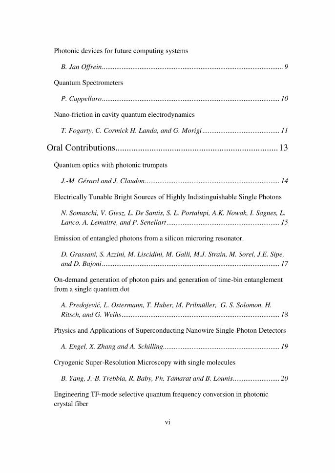
Quantum optics with photonic trumpets
J.-M. Gérard and J. Claudon ........................................................................... 14
Electrically Tunable Bright Sources of Highly Indistinguishable Single Photons
N. Somaschi, V. Giesz, L. De Santis, S. L. Portalupi, A.K. Nowak, I. Sagnes, L. Lanco, A. Lemaitre, and P. Senellart ............................................................... 15
Emission of entangled photons from a silicon microring resonator.
D. Grassani, S. Azzini, M. Liscidini, M. Galli, M.J. Strain, M. Sorel, J.E. Sipe, and D. Bajoni ................................................................................................... 17
On-demand generation of photon pairs and generation of time-bin entanglement
from a single quantum dot
A. Predojević, L. Ostermann, T. Huber, M. Prilmüller, G. S. Solomon, H. Ritsch, and G. Weihs ........................................................................................ 18
Physics and Applications of Superconducting Nanowire Single-Photon Detectors
A. Engel, X. Zhang and A. Schilling ................................................................. 19
Cryogenic Super-Resolution Microscopy with single molecules
B. Yang, J.-B. Trebbia, R. Baby, Ph. Tamarat and B. Lounis .......................... 20
Engineering TF-mode selective quantum frequency conversion in photonic
crystal fiber

vii
A. Eckstein, T. Hiemstra, S. Kolthammer, J. Nunn, and I. A. Walmsley .......... 21
Transport and harvesting of excitons mediated by strong coupling
J. Feist, C. Gonzalez-Ballestero, E. Moreno and F. J. Garcia-Vidal .............. 22
Ultrafast hybrid nonlinear plasmonics
H. Giessen, B. Metzger, M. Hentschel, L. Gui, Q. Ai, T. Schumacher, T. Weiss, M. Nesterov, M. Lippitz, B. Knabe, K. Buse, X.C. Ye, and C.B. Murray ......... 23
Second Harmonic Generation from Realistic Plasmonic Nanoantennas and Fano
Metamolecules
J. Butet and O. J.F. Martin .............................................................................. 24
Engineering non-classical states of light and matter in automatedly optimized
photonic crystal structures
V. Savona, H. Flayac and M. Minkov .............................................................. 26
Carbon synthesis in Prague and incorporation of optically active silicon colour
centres into diamond thin films
M. Varga, A. Kromka, et al. ............................................................................. 27
Room temperature Single Photon Sources in Silicon Carbide
S. Castelletto, A. Lohrmann, L. Rosa, B. C. Johnson, T. Ohshima, A. Gali..... 29
Controlled Routing of Single Plasmons at the Nanoscale
S. Kumar, N. Møller Israelsen, A. Huck and U. Lund Andersen ..................... 31
A low-loss, broadband dielectric antenna enabling highly efficient photon
collection from a coherent NV center spin in diamond
E. Neu, D. Riedel, D. Rohner, M. Ganzhorn, T. Kaldewey, P. Appel, R. J. Warburton, and P. Maletinsky ......................................................................... 32
Coupling effects in plasmonic nanoparticle arrays: the weak and the strong
coupling regime and the effects of spin-orbit coupling
T. K. Hakala, L. Shi, M. Kataja, A. Julku, H. T. Rekola, M. J. Huttunen, J.-P. Martikainen, R. J. Moerland, S. van Dijken, and P. Törmä ............................ 33

viii
Dynamics of a quantum emitter in nonlocal dissipative periodic structures
F. Intravaia, K. Busch ..................................................................................... 34
Role of collective superradiant modes on the spontaneous emission in a dense
cloud of atoms
N.J. Schilder, C. Sauvan, A. Browaeys, J.-P. Hugonin and J.-J. Greffet ......... 35
Optical diode based on the chirality of guided photons
C. Sayrin, C. Junge, R. Mitsch, B. Albrecht, D. O'Shea, P. Schneeweiss, J. Volz, A. Rauschenbeutel ................................................................................... 37
Optomechanics, a platform for nanoscale quantum optics
A. Xuereb.......................................................................................................... 38
Poster Presentations ..................................................................... 39
Evolution of 1D Airy beam propagating through a Zeeman EIT atomic medium
D. Arsenović, J. Dimitrijević and B. M. Jelenković ......................................... 40
Surface plasmons excitation in Kretschmann structure with waveguiding,
amplifying and nonlinear nanoscale cover layer
H.V. Baghdasaryan, T.M. Knyazyan, T.T. Hovhannisyan, M. Marciniak ...... 41
Cavity Quantum Electrodynamics with Quantum Dots
M.P. Bakker, A.V. Barve, T. Ruitenbeek, W. Löffler , L.A. Coldren, D. Bouwmeester, and M.P. van Exter ................................................................... 42
Second Harmonic generation from ZnWO4 single crystal and ZnWO4-ZnO
composites
A. Belardini, P. Osewski, E. Petronijevic, M. Centini, C. Sibilia, D. Pawlak . 43
Composite localized modes in discretized spin-orbit-coupled Bose-Einstein
condensates
P. P. Beličev, G. Gligorić, A. Maluckov, J. Petrović , Lj. Hadžievski and B. A. Malomed .......................................................................................................... 44

ix
Controlling Coherence in Epsilon-Near-Zero Metamaterials
H. Caglayan ..................................................................................................... 45
Infrared Thermal Emission by Multipolar Nanoantennas
M. Centini, A. Benedetti, M. C. Larciprete, A. Belardini, R. Li Voti, M. Bertolotti and C. Sibilia. .................................................................................. 46
One-dimensional sub-wavelength atom localization via Zeeman EIT in a
degenerate two-level system
J. Dimitrijević, D. Arsenović and B. M. Jelenković ......................................... 47
Photonics of metal oxides: Formation of organic molecules over their surfaces
M. Ferus, S. Civiš and P. Kubelík .................................................................... 48
Photon detectors based on High Tc Superconductors
C. Feuillet-Palma, N. Bergeal and J. Lesueur ................................................. 49
Proposal for an all-silicon integrated single-photon source by unconventional
photon blockade
H. Flayac, D. Gerace and V. Savona............................................................... 50
Micro-photoluminescence study of local emission of Quantum Dots in Core-Shell
GaAs/AlGaAs Nanowires
L. Francaviglia, Y. Fontana, G. Tütüncüoglu, F. Matteini, H. Potts, S. Conesa-Boj, J. Arbiol, A. Fontcuberta i Morral ........................................................... 51
Addressing a single photon source by a nanowaveguide
W. Geng, M. Manceau, N. Rahbany, V. Sallet, M. De Vittorio , L. Carbone, Q. Glorieux, A. Bramati, C. Couteau .................................................................... 52
Spectral Dynamics of NV centers in the vicinity of a mirror
N. M. Israelsen, J. S. Neergaard-Nielsen, U. L. Andersen and A. Huck .......... 54
Nonequilibrium terahertz conductivity in materials with localized electronic
states

x
V. Janković and N. Vukmirović ........................................................................ 55
Controlling the emission quantum efficiency of Er3+
ions by near-field coupling
with plasmonic nanohole array
B. Kalinic, T. Cesca, N. Michieli, C. Maurizio, P. Mazzoldi, G. Mattei .......... 56
Absence of mutual polariton scattering for strongly coupled surfa ce plasmon
polaritons and dye molecules with a large Stokes shift
M.A. Koponen, U. Hohenester, S. Baieva, and J.J. Toppari ............................ 57
Nanostructuring of multilayered thin films by femtosecond laser beam
A. G. Kovačević, S. Petrović, A. Beltaos, U. Ralević, A. Matković, B. Vasić, R. Gajić, and B. Jelenković .................................................................................. 59
High intensity broadband source of energy-entangled photons for spectroscopy
S. Lerch and A. Stefanov .................................................................................. 60
Single molecule fluorescence coupled to dielectric waveguides: a new route
towards integrated single photon sources
P. Lombardi, M. Maccari, S. Rizvi, G. Mazzamuto, and C. Toninelli, G. Kewes, O. Neitzke, A. W. Schell, J. Probst, J. Wolters, and O. Benson .......... 61
One-dimensional superconducting photonic crystal with dielectric defect layer
I.L. Lyubchnskii, A.E. Zabolotin, N.N. Dadoenkova, Yu.S. Dadoenkova, and Y.P. Lee ............................................................................................................ 62
Entanglement with negative Wigner function of 3000 atoms heralded by a single
photon
R. McConnell, H. Zhang, J. Hu, S. Ćuk and V. Vuletić .................................... 63
A Pulsed Nonclassical Light Source Driven by an Integrated Electrically
Triggered Quantum Dot Microlaser
P. Munnelly, T. Heindel, M. M. Karow, S. Höfling, M. Kamp, C. Schneider, and S. Reitzenstein ........................................................................................... 64

xi
Wavelenght filtering of the emission at 1.3 m of a single InAs quantum dot by using a tunable fibre Bragg grating
G. Muñoz-Matutano, D. Rivas, A. Ricchiuti, D. Barrera, C. R. Fernández-Pousa, L. Seravalli, G. Trevisi, P. Frigeri, S. Sales, J. Martínez-Pastor ......... 65
Propagation of Raman–Ramsey pulses through Rb buffer gas cell under condition
of Zeeman Electromagnetically Induced Transparency
S. N. Nikolić, M. Radonjić, N. M. Lučić, A. J. Krmpot, and B.M. Jelenković .. 67
Propagation and survival of frequency-bin entangled photons in metallic
nanostructures
L. Olislager, B. Kolaric,, W. Kubo, T. Tanaka, R. A. L. Vall e , P. Emplit, and S. Massar.......................................................................................................... 68
Electromagnetically induced transparency in spherical quantum dot with on-
center hydrogen impurity in magnetic field
V. Pavlović and Lj. Stevanović ......................................................................... 69
Perforated SOI Microring Resonators for Enhanced Light Matter Interaction
R. Petruškevičius, D. Urbonas, M. Gabalis, K. Vaškevičius, A. Balčytis, S. Juodkazis .......................................................................................................... 70
Different strategies towards the deterministic coupling of a Single Quantum Dot
to a Photonic Crystal Cavity Mode
I.Prieto, J.Herranz, Y.González, P.A.Postigo, B.Alén, L.González, J.Martín‐Sánchez, L.J.Martínez, M.Kaldirim, D. Fuster, J.Canet‐Ferrer,
G.Muñoz‐Matutano, and J.Martínez‐Pastor .................................................... 71
Polaron transport in nanocrystal solids
N. Prodanović, N. Vukmirović ......................................................................... 72
Directional couplers based on open and closed waveguide arrays
A. Radosavljević, J. Petrovic, A. Daničić, A. Maluckov and L. Hadžievski ..... 73
Operating Quantum Dot Single-Photon Sources Using a Compact Stirling
Cryocooler

xii
A. Schlehahn, M. Gschrey, J.-H. Schulze, S. Rodt, A. Strittmatter, T. Heindel, and S. Reitzenstein ........................................................................................... 74
White light generation and non-linear optical properties of Ag nanoclusters and
nanoparticles dispersed in the glass host
M. V. Shestakov, V. E. Kaydashev , H. Hanh Mai , E. Janssens, M. Meledina, S.Turner, P. Lievens, G.Van Tendeloo and V. V. Moshchalkov ....................... 75
Slow-Light Metamaterials
P. Tassin ........................................................................................................... 77
Bright Emission of Indistinguishable Photons from Deterministically Fabricated
Quantum Dot Microlenses
A. Thoma, P. Schnauber, M. Gschrey, R. Schmidt, B. Wohlfeil, M. Seifried, J.-H. Schulze, S. Burger, F. Schmidt, A. Strittmatter, S. Rodt, T. Heindel, S. Reitzenstein ...................................................................................................... 78
Azophenylcarbazoles: isomerization and application to functionalize GaN
surface.
R.Tomašiūnas, A.Balčytis, G.Seniutinas, V.Bikbajevas, R.Petruškevičius, V.Getautis......................................................................................................... 79
Metamorphic InAs/InGaAs nanostructures for single QD emission in the telecom
range
G. Trevisi, L. Seravalli, G. Muñoz-Matutano, D. Rivas, J. Martinez-Pastor and P. Frigeri.......................................................................................................... 81
Progress in the fabrication of open-access microcavities using focused ion beam
milled substrates
A. Trichet, S. Johnson, P. Dolan and J. Smith ................................................. 82
Near-Field Optical Detection of Plasmon Resonances
C. Triolo, S. Trusso, S.Patanè, S. Savasta and R.Saija ................................... 83
Quantum Communications along free-space and satellite channels: a workbench
for Nanoscale Quantum Processes

xiii
G. Vallone, D. Dequal, M. Tomasin, M. Schiavon, and P. Villoresi .............. 84
Ab initio dielectric responses as a basis for computational plasmonics and
photonics
R. Warmbier, A. Quandt................................................................................... 85
Analytical formalism for the interaction of two-level quantum emitters with
plasmonic nanoresonators
J. Yang, P. Lalanne, M. Perrin, ....................................................................... 87
Generation and Detection of Single Photons: Applications in Quantum
Communication
H. Zbinden........................................................................................................ 88
Parametric non-degenerate four wave mixing in hot potassium vapor
B. Zlatković, A. Krmpot, N. Šibalić, B. M. Jelenković, M. Radonjić ................ 89
Meeting Participants .................................................................... 91

xiv

1
GUEST SPEAKERS

2
Quantum nanophotonics
Jelena Vuckovic
Ginzton Laboratory, Spilker Building for Engineering and Applied Sciences Stanford University , 348 Via Pueblo Mall , Stanford, CA 94305-4088, USA
email: [email protected]
By embedding a single quantum emitter inside a nanoresonator that strongly
localizes optical field, it is possible to achieve a very strong light –matter
interaction. The strength of this interaction is characterized by the coherent emitter-
field coupling strength (g), which increases with reduction in the optical mode
volume and which also sets the limit on the operational speed of such a system.
With InAs quantum dots inside GaAs photonic crystal cavities, coupling strengths
of 40 GHz can be reached (much greater than the record values in atom-cavity QED
systems), while nanometallic cavities could increase them over 100GHz, as a result
of the further reduction in the mode volume. Such a quantum dot-nanocavity
platform is of interest for various quantum technologies, as well as in optical
switching/computing [1,2].
Finally, alternative material systems such as impurities in silicon carbide [3] or
diamond that could potentially bring the described experiments to the room
temperature regime are investigated, as well as the applications beyond quantum
technologies, including optical switches and biosensors.
REFERENCES
[1] On-chip generation of indistinguishable photons using cavity quantum-
electrodynamics, Kai Müller, Armand Rundquist, Kevin A. Fischer, Tomas
Sarmiento, Konstantinos G. Lagoudakis, Yousif A. Kelaita, Carlos Sanchez Munoz,
Elena del Valle, Fabrice P. Laussy, Jelena Vuckovic (arXiv:1408.5942)
[2] Ultrafast Photon-Photon Interaction in a Strongly Coupled Quantum Dot-Cavity
System, Dirk Englund, Arka Majumdar, Michal Bajcsy, Andrei Faraon, Pierre
Petroff, and Jelena Vuckovic, Physical Review Letters 108, 093604 (2012)
[3] Visible Photoluminescence from Cubic (3C) Silicon Carbide Microdisks
Coupled to High Quality Whispering Gallery Modes, Marina Radulaski, Thomas M.
Babinec, Kai Müller, Konstantinos G. Lagoudakis, Jingyuan Linda Zhang, Sonia
Buckley, Yousif A. Kelaita, Kassem Alassaad, Gabriel Ferro, and Jelena
Vuckovic, ACS Photonics (2014)

3
Modeling of Nitride Nanostructure Based Classical and
Non-Classical Light Emitters
σenad Vukmirović1, Stanko Tomić2 and Žarko Gačević3
1Scientific Computing Laboratory, Institute of Physics Belgrade, Serbia 2Joule Physics Laboratory, University of Salford, Manchester, United Kingdom
3ISOM - ETSIT, Universidad Politécnica de Madrid, Spain email: [email protected]
Nanostructures based on III-nitride semiconductors offer certain advantages for
realization of single-photon sources. Larger band offsets and effective masses lead
to strong quantum-confinement effects which enable the operation of single-photon
sources at higher temperatures. Wide band gap of III-nitrides leads to the emission
in the blue and ultraviolet spectral range, which is not accessible with most of the
other materials. In this talk, simulation insights into the classical and non-classical
light emission properties of III-nitride nanostructures will be discussed.
In the first part of the talk, calculations of excitonic and biexcitonic states in self-
assembled GaN/AlN quantum dots will be presented with special emphasis on the
use of these dots for single-photon source applications [1]. Theoretical methodology
for the calculation of single-particle states was based on 8-band strain-dependent
envelope function Hamiltonian, with the effects of spin-orbit interaction, crystal-
field splitting, and piezoelectric and spontaneous polarizations taken into account.
Exciton and biexciton states were found using the configuration-interaction method.
Optimal dot heights for their use in single-photon emitters were determined for
various diameter-to-height ratios.
In the second part of the talk, electronic properties of InGaN quantum structures
embedded in site controlled GaN nanowires will be presented [2]. The InGaN
structures under consideration consist of two sections: the middle one, which is
formed on the polar c-facet, and the side one, which is formed on the semi-polar r-facets. These structures exhibit two-color emission at 384 nm and 488 nm. We
identify that the main origin of two-color emission is higher In incorporation on the
nanowire polar c-facet, while the influences of internal electric field and strain are
less significant.
REFERENCES
[1] S. Tomić and σ. Vukmirović, Phys. Rev. B 7λ, 245330 (200λ). [2] Ž. Gačević, N. García-Lepetit,
σ. Vukmirović, et al, in preparation.

4
Complexity of natural photonic structures
Dejan V. Pantelić1
1Institute of Physics, University of Belgrade, Serbia email: [email protected]
Photonic structures are ubiquitous in nature [1] – ranging from insect eyes, cuticle
and wings, bird feathers and cuttlefish bone, to stones and minerals, to mention just
a few. Optically interesting features are very intricate and range from nanometer to
micrometer level. They are simultaneous combination of ordered and disorder [2],
resulting in complicated diffraction gratings with defects (surface, volume or
layered), scatterers and photonic crystals.
Here we deal with internal complexity of biological structures in terms of their
internal geometry and a number of resulting optical effects – iridescence,
polarization, photonic band-gap, scattering, dispersion, fluorescence, diffraction,
interference... The number of degrees of freedom is so large that there is an
extremely small probability of finding two identical structures.
We propose attaching a biological structure into an item (a bill, a document, or a
product), thus making it as unique as an individual human being with its fingerprint,
retinal veins, or iris colour and pattern. The natural variability of biological
processes guarantees the uniqueness, in the same way as no two fingerprints are
identical. The uniqueness is expressed by multiple optical features randomly
distributed across the structure. Furthermore, natural structures can be artificially
modified or functionalized by direct laser writing to include other overt or covert
information.
The advantage is that there is no need for complicated manufacturing of micro and
nanostructures [3]. They grow by themselves in huge numbers, each one being
unique and extremely complicated to counterfeit.
REFERENCES
[1] T. Starkey, P. Vukusic, Nanophotonics 2 289–307 (2013)
[2] D. S. Wiersma, Nature Photonics 7 188-196 (2013)
[3] R. L. van Renesse, Optical document security, Artech House, (2004)

5
INVITED SPEAKERS

6
Quantum optics with quantum-dot spins and photons
Mete Atatüre
Cavendish Laboratory, University of Cambridge, Cambridge, United Kingdom
email: [email protected]
Spins confined in solids, such as quantum dots and atomic impurities provide
interesting and rich physical systems. Their inherently mesoscopic nature leads to a
multitude of interesting interaction mechanisms of confined spins with the solid
state environment of spins, charges, vibrations and light. Implementing a high level
of control on these constituents and their interactions with each other creates
exciting opportunities for realizing stationary and flying qubits within the context of
spin-based quantum information science. I will provide a snapshot of the progress
and challenges for optically interconnected spins, as well as first steps towards
hybrid distributed quantum networks involving other physical systems.

7
Ultrafast Coherent Charge Transfer in Solar Cells and Artificial
Light Harvesting Systems: Toward Movies of Electronic Motion
Christoph Lienau1
1Institute of Physics, Carl von Ossietzky University, Oldenburg, Germany email: [email protected]
The efficient conversion of (sun-)light into electrical or chemical energy is one of
the most fundamental and relevant challenges in current energy research. Our
ability to construct artificial molecular or nanostructured devices that can harvest
and exploit sunlight inevitably relies on an in-depth understanding of the elementary
microscopic principles that govern the underlying light conversion processes.
Generally, these processes happen on an exceedingly short femtosecond time scale,
making real time studies of the light-driven dynamics particularly important. To
elucidate these dynamics, we have recently combined coherent femtosecond
spectroscopy and first-principles quantum dynamics simulations [1,2] and have
used this approach to explore the primary photoinduced electronic charge transfer in
two prototypical structures: (i) a carotene-porphyrin-fullerene triad, an elementary
component for an artificial light harvesting system [2] and (ii) a polymer:fullerene
blend as a model for an organic solar cell [1].
Surprisingly, our results provide strong
evidence that in both systems, at room
temperature, the driving mechanism of
the primary step within the current
generation cycle is a quantum-
correlated wavelike motion of electrons
and nuclei on a timescale of few tens of
femtoseconds. Our results suggest that
the strong coupling between electronic
and vibrational degrees of freedom is of
key importance for the dynamics and
yield of the charge separation process. In my talk, I will present our most recent
findings and their implications for the light-to-current conversion in solar cells.
REFERENCES
[1] S. M. Falke et al., Coherent ultrafast charge transfer in an organic photovoltaic
blend. Science 344, 6187 (2014).
[2] C. A. Rozzi et al. Quantum coherence controls the charge separation in a
prototypical artificial light harvesting system. Nature Comm. 4, 1602 (2013).
Real time simulation of the coherent charge
transfer dynamics between polymer and
fullerene moiety in a P3HT/PCBM thin film
photovoltaic device

8
Quantum Optics with Nanowires
V. Zwiller1, 2
, K. Jöns2, M. Reimer
2, G. Bulgarini
2, M. Bouwes Bavinck
2, L.
Schweickert2, I. Esmaeil Zadeh
2, J. Zichi
2
1Applied Physics, KTH, Stockholm, Sweden 2 Kavli Institute of Nanoscience, TU Delft, Netherlands
email: [email protected]
Nanowires offer new opportunities for nanoscale quantum optics; the quantum dot
geometry in semiconducting nanowires as well as the material composition and
environment can be engineered with unprecedented freedom to improve the light
extraction efficiency.
Quantum dots in nanowires are shown to be efficient single photon sources, in
addition because of the very small fine structure splitting, we demonstrate the
generation of entangled pairs of photons from a nanowire.
By doping a nanowire and making ohmic contacts on both sides, a nanowire light
emitting diode can be obtained with a single quantum dot as the active region.
Under forward bias, this will act as an electrically pumped source of single photons.
Under reverse bias, an avalanche effect can multiply photocurrent and enables the
detection of single photons.
Another type of nanowire under study in our group is superconducting nanowires
for single photon detection, reaching efficiencies, time resolution and dark counts
beyond currently available detectors. We will discuss our first attempts at
combining semiconducting nanowire based single photon emitters and
superconducting nanowire single photon detectors on a chip to realize complete
quantum circuits on a chip.

9
Photonic devices for future computing systems
Bert Jan Offrein
IBM Research – Zurich, Säumerstrasse 4, 8803 Rüschlikon, Switzerland email: [email protected]
Photonic technology is now emerging in computing systems as a means to provide
the required interconnect bandwidth between racks and boards. In addition to the
larger bandwidth x length product as in electrical links, optical communication
offers a higher interconnect density and power efficiency. To further scale the
performance of future cloud, datacenter and server systems optical technology must
be integrated deep into the system, closely packaged with electrical functions such
as the processor, switch or memory. However, today’s hybrid optical technology solutions suffer from the large number of components and associated assembly cost.
Silicon photonics extends established CMOS technology with optical functions such
as electro-optic modulators, detectors and wavelength filter devices for wavelength
division multiplexing offering a path to a higher state of integration [1]. This opens
prospects for scalable and cost-effective electro-optical functions in silicon but also
at system-level, novel assembly and optical signal distribution technologies have to
be established. At the Photonics
group of IBM Research – Zurich
we explore both aspects. Novel
silicon photonics devices for
power-efficient optical links were
demonstrated. For example an
optical modulator with <50 fJ
switching energy [2] and high Q/V
silicon photonics optical cavities [3]. Single mode polymer waveguides provide a
scalable optical interface between silicon photonics chips and the system [4].
Exploring technologies for alternate computing concepts, we demonstrated Bose-
Einstein Condensate formation at room temperature in a polymer with potential
applications in quantum simulations [5].
REFERENCES
[1] S. Assefa, et al., IEEE IEDM, pp. 33.8.1–33.8.3 (2012)
[2] J. Hofrichter, et al., Optics Express, Vol. 20 Issue 9, pp. 9363-9370 (2012)
[3] P. Seidler, et al., Optics Express, Vol. 21 Issue 26, pp. 32468-32483 (2013)
[4] R. Dangel, et al., Optics Express, Vol. 23 Issue 4, pp. 4736-4750 (2015)
[5] T. Stoeferle, et al., Nature Materials, 13, pp. 247–252 (2014)
Vision for a computing board with processor
packages and memory indicating embedded
electrical and optical interconnects.

10
Quantum Spectrometers
Paola Cappellaro1
1 Nuclear Science and Engineering Department, Massachusetts Institute of Technology, Cambridge, MA
email: [email protected]
Quantum control techniques have proven effective to extend the coherence of qubit
sensors, thus allowing quantum-enhanced sensitivity at the nano-scale. For
example, simple pulsed dynamical decoupling schemes can protect against
decoherence by acting as noise filters, while preserving the interaction with the
system or field that one wishes to measure.
Nuclear spin imaging with a shallow NV
center in diamond. A single NV spin at 1-
2nm from the diamond surface can sense
single nuclear spins in a molecule (the
chemokine receptor CXCR4) anchored to
the diamond. The magnetic field produced
by individual C13 is in the range of nT,
within reach of NV sensitivity. In the inset:
the binding site of interest (atoms other than
C13 are blue (O) and red (N)).
In this talk I will show how we can engineer the evolution of quantum sensor by
creating more general dynamic filters that help reveal temporal and spatial
information about classical and quantum sources.
The high frequency resolution achieved by these dynamical filters turns the
quantum sensors into accurate spectrometers, capable of detecting the dynamics of
external fields or of imaging the spatial configuration of a spin bath.
I will illustrate applications of these strategies in experimental implementations
based on the Nitrogen-Vacancy center in diamond, which shows promise for the
detection of biological signals and for the reconstruction of protein structures [1].
REFERENCES
[1] A. Ajoy, U. Bissbort, M. D. Lukin, R. L. Walsworth and P. Cappellaro, Phys.
Rev. X 5, 011001 (2015)

11
Nano-friction in cavity quantum electrodynamics
Thomas Fogarty1, Cecilia Cormick
2 Haggai Landa
3, and Giovanna Morigi
1
1Theoretische Physik, Universität des Saarlandes, D-66123 Saarbrücken, Germany 2 G, C N C T and niversidad Nacional de C ordoba, Ciudad niversitaria,
LA , C rdoba, Argentina 3 Univ. Paris Sud, CNRS, LPTMS, UMR 8626, Orsay 91405, France
email: [email protected]
The Frenkel-Kontorova model reproduces in one dimension the essential features of
the stick-slip motion which is characteristic of friction. We theoretically analyze a
realization where the atomic array is an ion chain and the substrate potential is the
optical lattice of a high-finesse resonator, as sketched in subplot (a). The ion
transitions strongly couple with the cavity
mode, and constitute a dynamically-
refractive medium, which determines the
potential depth. In this regime the cavity
potential behaves like a deformable
substrate. We characterize the properties
of the stationary state, resulting from the
balance between a pump driving the
resonator and losses due to cavity decay,
when the interparticle distance and the
potential wavelength are incommensurate.
While the sliding phase is essentially
independent of the cavity nonlinearity C, for increasing cavity coupling the
transition to the pinned phase occurs at decreasing values of the pump strength, as
sketched in subplot (b), and can exhibit bistability. This dynamics represents a
paradigm of competing selforganizing mechanisms at the quantum limit which can
be observed in existing experimental setups [1].
REFERENCES
[1] T. Fogarty et al.. preprint (2015).

12

13
ORAL CONTRIBUTIONS
14
Quantum optics with photonic trumpets
Jean-Michel Gérard and Julien Claudon
1Institute for Nanoscience and Cryogeny, CEA, Grenoble, France
email: [email protected]
Optimizing the coupling between a localized quantum emitter and a single-mode
optical channel represents a powerful route to realize bright sources of non-classical
light states for QIPC. Reversibly, the efficient absorption of a photon impinging on
the emitter is key to realise a spin-photon interface, the node of future quantum
networks.
Besides optical microcavities, photonic wires are
very attractive in this context [1]. We introduce
the Photonic Trumpet [2], formed by a high-index
single-mode waveguide and a conical tapering.
Nearly perfect single mode emission, low-
divergence Gaussian radiation pattern, linear
polarization control and high efficiency single
photon emission (> 0.75 photon per pulse) are
reported for a single quantum dot embedded in a
Photonic Trumpet. We also demonstrate a
broadband tuning of the emission wavelength
without efficiency loss using strain-effects. More
generally, this novel photonic microstructure
appears as a very promising platform to explore
the unique optical properties of “one-dimensional
atoms”[3] and hybrid optomechanical systems where the interaction between the two-level
quantum system and mechanical modes is
mediated by strain [4].
REFERENCES
[1] J. Claudon et al, Nature Photonics 4, 174 (2010).
[2] M. Munsch et al, Phys. Rev. Lett. 110, 177402 and 239902(E) (2013)
[3] D. Valente et al, New J. Phys 14, 083029 (2012); Phys Rev A 86, 022333 (2012)
[4] I. Yeo et al, Nature Nanotechnology 9, 106 (2014)
Au+ SiO2
mirror
1 µm
adiabatic
taper
anti-
reflection
coating
InAs QD
Scanning electron
micrograph of a GaAs
photonic trumpet.

15
Electrically Tunable Bright Sources of Highly Indistinguishable
Single Photons
N. Somaschi1, V. Giesz
1, L. De Santis
1, S. L. Portalupi
1, A.K. Nowak
1, I. Sagnes
1, L.
Lanco1,2
, A. Lemaitre1, and P. Senellart
1,3
1 Laboratoire de Photonique et Nanostructures-CNRS, Marcoussis, France 2 Université Paris Denis - Diderot - Paris 7, Paris, France
3 Département de Physique, Ecole Polytechnique, Palaiseau, France email: [email protected]
Semiconductor quantum dots (QDs) are very promising systems to build a solid
state quantum network, especially with the possibility to fabricate bright sources of
single and indistinguishable photons. Recently, we demonstrated single photon
sources with brightness of 80% and indistinguishability as high as 92% by inserting
QDs in micropillar cavities [1].
Here we report on the fabrication of electrically tunable ultrabright sources of
indistinguishable single photons. We propose a novel cavity design which permits
to apply an electric field while maintaining a 3D confinement for the photons: it
consists of a micro-pillar cavity (2-3 m) connected to a larger ohmic-contact
a) Schematic of the connected–pillar device. b, c) -scope image
and PL intensity map of the device. d) PL contour plot recorded at
different applied voltage showing the exciton line shift across the
cavity mode. e, f) Second order autocorrelation function g(2)( ) in a
an HBT(e) and HOM (f) experiment showing high single photon
purity and indistinguishability of the source.

16
surface with four 1D-bridges and a surrounding frame (Fig. 1a). Laterally, the
fundamental cavity mode (CM) of the structure is confined in the centre of the
connected pillar. Vertically, the GaAs cavity is surrounded by GaAs/AlGaAs Bragg
mirrors, doped in a p-i-n diode configuration. A single QD is deterministically
positioned at the center of the pillar by means of an advanced in-situ optical
lithography (Fig. 1b, c) [2, 3]. The strong Purcell effect obtained with such device
results in a very high brightness of the single-photon source, exceeding 55%.
Furthermore the application of an electric field results in a Stark shift of the QD
transition over a few nm spectral range, allowing a fine spectral tuning within the
mode (Fig. 1d). Under non-resonant excitation, we demonstrate a photon
indistinguishability in the 70-to 80% range (Fig. 1f). This structure allows strictly
resonant excitation where the photons are shown to be perfectly indistinguishable.
REFERENCES
[1] O. Gazzano et at., Nat.Comm. 4, 1425 (2013)
[2] A. Dousse et at., Phys. Rev. Lett. 101, 267404 (2008)
[3] A. Nowak et al., Nat.Comm. 5, 3240 (2014).

17
Emission of entangled photons from a silicon microring resonator.
D. Grassani1, S. Azzini
1, M. Liscidini
1, M. Galli
1, M.J. Strain
2, M. Sorel
3, J.E. Sipe
4, and
D. Bajoni5
1Institute 1 Dipartimento di Fisica, Università di Pavia, 27100 Pavia, Italy 2 Institute of Photonics, University of Strathclyde, Glasgow G4 0NW, UK 3 School of Engineering, University of Glasgow, Glasgow G12 8LT, UK
4 Department of Physics and Institute for Optical Sciences, University of Toronto, 60 St. George Street, Ontario, Canada
5 Dipartimento di Ing. Ind. Inf., Università di Pavia, 27100 Pavia, Italy email: [email protected]
Entanglement is a fundamental tool in a wide variety of quantum information
protocols, among others quantum cryptography and quantum information
processing. An ideal integrated source of entangled photons should be CMOS
compatible for cheap production, easily integrable with fiber networks, and highly
repeatable. In this work (Optica 2 88–94 (2015)) we report on a novel source of
entangled photon pairs integrated on a silicon chip. Our sample, a silicon micro-ring
with radius of 10 m (Fig 1 (a)), emits signal and idler photon pairs by spontaneous four wave mixing. Entanglement is verified via a Franson type experiment (Fig. 1
(b)(c)). This source of entangled photons has unique characteristics. The spectral
brightness per coupled pump power is remarkable, ∼ 6 × 10⁷ nm
−1 mW
−2 s
−1 , more
than four order of magnitudes larger than that reported for entangled photon pairs
emitted by cm long silicon waveguides. The ring small footprint has great
advantages for scalability, its micrometric size making it ideal for integration with
other photonic devices on the same chip.
a) Micrograph of the sample. (b) Time correlation curve for a coupled pump power of 1
mW. The letters S and L refer to the paths takes by the signal and idler photons in the
short (S), and long (L) arms of two independent interferometers, blue for signal and red
for idler. (c). Height of the central peak from panel (b) as a function of the total phase
(dots) and best fit to a sinusoid (red dashed line).

18
On-demand generation of photon pairs and generation of time-bin
entanglement from a single quantum dot
Ana Predojević1, Laurin Ostermann
2, Tobias Huber
1, Maximilian Prilmüller
1,
Glenn S. Solomon3, Helmut Ritsch
2, and Gregor Weihs
1
1Institute for Experimental Physics, University of Innsbruck, Innsbruck, Austria 2 Institute for Theoretical Physics, University of Innsbruck, Innsbruck, Austria 3Joint Quantum Institute, National Institute for Standards and Technology and
University of Maryland, Gaithersburg, United States
email: [email protected]
Quantum information processing needs novel, efficient, and compact sources of
single photons and entangled photons pairs. We report here the resonant two-photon
excitation of the biexciton state of a single InAs quantum dot embedded in a micro-
cavity [1]. This method allows us to generate photon pairs with nearly unit
probability. The resonant nature of the excitation was confirmed by the observation
of Rabi oscillations. In addition, we measured the level of quantum coherence in the
ground-biexciton state superposition by performing a Ramsey interference
measurement. Also, and to our knowledge for the first time, we performed a
measurement of the spin-echo in such a system.
In addition, we report on an unprecedented level of time-bin entanglement [2] from
a single quantum dot. The requirements to generate this type of entanglement
include the suppression of the single exciton amplitude in the excitation pulse and
negligible dephasing caused by the laser excitation. These conditions constitute
contradictory demands on the excitation pulse-length and its intensity. We
performed a study of these limitations from both an experimental and a theoretical
point of view and we identified key parameters required in order to achieve a high
degree of time-bin entanglement from a quantum dot system. We measured the
entanglement in this optimized regime and the results yield the concurrence of
0.78(6) and fidelity of 0.88(3) to the maximally entangled state.
REFERENCES
[1] H. Jayakumar, A. Predojević, T. Huber, T. Kauten, G. S. Solomon, G. Weihs, Phys. Rev. Lett. 110 135505 (2013).
[2] H. Jayakumar, A. Predojević, T. Kauten, T. Huber, G. S. Solomon, and G.Weihs, Nature Communications 5 4251 (2014).

19
Physics and Applications of Superconducting Nanowire Single-
Photon Detectors
Andreas Engel, Xiaofu Zhang and Andreas Schilling
Institute of Physics, University of Zurich, Switzerland
email: [email protected]
Superconducting nanowire single-photon detectors (SNSPD) have attracted a lot of
interest in recent years, due to their unique combination of characteristics. They are
characterized by low-timing jitter, high count rates, high detection efficiency and
low dark counts. This makes them detectors of choice for a wide variety of
applications, from quantum key distribution and interplanetary communications to
cancer research, to name just a few.
In order to simultaneously obtain above mentioned characteristics, it is necessary to
realize various optimizations [1], e.g. the use of optical cavities to increase the
photon absorption, or the reduction of thermal background radiation to reduce dark
counts. These technological advances have recently been matched by an improved
understanding of the detection mechanism [2, 3], which indicates that magnetic
vortices are essential for photon detection in SNSPD. We will present our current
understanding of the detection mechanism and highlight some results also important
for applications. Furthermore, we will discuss preliminary results that give an
indication of why SNSPD made from WSi show some remarkable differences as
compared to SNSPD based on NbN and similar materials [4].
REFERENCES
[1] E. A. Dauler et al., Opt. Eng., 53 081907 (2014).
[2] A. Engel and A. Schilling, J. Appl. Phys., 114, 214501 (2013).
[3] A. N. Zotova and D. Y. Vodolazov, Supercond. Sci. Technol., 27, 125001
(2014).
[4] A. Engel et al., IEEE Trans. Appl. Supercon., 25, 2200407 (2015).
20
Cryogenic Super-Resolution Microscopy with single molecules
B. Yang1,2
, J.-B. Trebbia1,2
, R. Baby1,2
, Ph. Tamarat1,2
and B. Lounis1,2
1Univ Bordeaux, LP2N, F-33405 Talence, France 2 nstitut d’ ptique & CNRS, LP2N, -33405 Talence, France
email: [email protected]
The controlled, coherent manipulation of quantum systems is an important
challenge in modern science and engineering, with significant applications in
quantum technologies. Solid-state quantum emitters such as single molecules,
quantum dots and NV centers in diamond are among the promising candidates for
realization of quantum bits. Arrays of strongly interacting solid-state quantum
systems are appealing platforms for the preparation of collective delocalized states
formed by the entanglement of individual emitters. For these systems, dipole-dipole
coupling occurs on nanometers scale and therefore experimental schemes which
optically resolve quantum emitters at this scale and allow the manipulation of their
degree of entanglement are crucial.
Although the various super-resolution microscopy techniques are now commonly
used at room temperature e.g. in biology, their extension to low temperatures is in
its infancy, mainly because of the inherent experimental complications due to the
use cryogenic systems and the non-adequacy of the photo-physics of usual markers
at these temperatures. We will present two super-resolution optical microscopy
techniques with single molecules. Organic molecules inserted in well-suited solid
matrix at liquid helium temperature are simple two-level systems on which quantum
entanglement experiments can be performed. We demonstrate a resolution down to
4 nm (FWHM) with DBATT molecules in octadecane at 2K. This technique
provides the unique possibility to super-resolve single molecules having close
optical resonances and can therefore bring quantum optics applications such as
studying the interactions and entanglements between single molecules.

21
Engineering TF-mode selective quantum frequency conversion in
photonic crystal fiber
Andreas Eckstein1, Thomas Hiemstra
1, Steve Kolthammer
1, Joshua Nunn
1, and Ian A.
Walmsley1
1Ultrafast Quantum Optics and Optical Metrology, Department of Physics, University of Oxford
email: [email protected]
Quantum frequency conversion [1] is a promising tool to translate quantum states of
light to a different wavelength regime, e. g. to improve detection efficiencies of
states at the single photon level [2]. Exploiting dispersion, it is possible to
implement a time-frequency (TF) mode selective conversion, quantum pulse gate
(QPG) [3], in order to [de-]multiplex from/into spectrally overlapping yet
orthogonal modes, boosting the transmission capacity of a single optical link while
minimizing degrading effects due to chromatic dispersion. However, the
requirements on phase-matching the nonlinear optical processes involved means
that application is restricted to a narrow range of wavelengths.
The emergence of micro-structured
photonic crystal fiber (PCF) has made it
possible to tailor optical dispersion profiles
to the application at hand. For four-wave-
mixing, the dominant nonlinear interaction
of light in silica, this means that phase-
matching can be achieved in settings not
accessible to standard optical fiber [4]. We
explore the enlarged parameter space for
implementing a QPG with the additional
freedom of engineering the material
dispersion function, and explore its
feasibility and possible roadblocks for application in quantum state engineering.
REFERENCES
[1] P. Kumar, Opt. Lett. 15, 1476-1478 (1990)
[2] S. Tanzilli, W. Tittel, M. Halder, O. Alibart et al., Nature 437, 116-120 (2005)
[3] B. Brecht, A. Eckstein, A. Christ et al., New J. Phys. 13, 0605029 (2011)
[4] C. Soeller et al., Phys. Rev. A 81 031801(R) (2010); H. J. McGuiness et al.,
Phys. Rev. Lett. 105, 093604 (2010)
Pulse-demultiplexing with a QPG: A
input pulse is decomposed into the gate’s mode basis, and the gating pulse selects
the mode to be converted.

22
Transport and harvesting of excitons mediated by strong coupling
J. Feist1, C. Gonzalez-Ballestero
1, E. Moreno
1 and F. J. Garcia-Vidal
1,2
1Departamento de sica Te rica de la Materia Condensada and Condensed Matter P ysics Center MAC , niversidad Aut noma de Madrid, Madrid, Spain
2Donostia International Physics Center (DIPC), Donostia/San Sebastian, Spain
email: [email protected]
The transport of excitons is a fundamental process that plays a crucial rule both in
natural phenomena such as photosynthesis, where energy has to be transported to a
reaction center, and in artificial devices such as organic solar cells, whose power
conversion efficiency can be improved significantly when the exciton diffusion
length is increased. However, most systems composed of organic molecules are
disordered and possess relatively large dissipation and dephasing rates, such that
exciton transport typically is inefficient.
Very recently, an increase of the electrical conductance of an organic material was
shown under strong coupling of the excitons to a cavity mode [1]. Strong coupling
is achieved when the energy exchange rate between exciton and electromagnetic
field modes becomes faster than the decay and decoherence rates of either
constituent. Inspired by this result, we demonstrate that exciton conductance in
organic materials can be enhanced by several orders of magnitude when the
molecules are strongly coupled to an electromagnetic mode. Using a 1D model
system, we show how the formation of a collective strongly coupled mode (a
polariton) allows excitons to bypass the disordered array of molecules and jump
directly from one end of the structure to the other [2].
We furthermore show that by designing the electric field profile of the
electromagnetic mode that provides the strong coupling, the transport properties can
be tuned to achieve exciton harvesting, i.e., to guide excitons from a collection area
to a specific location. We demonstrate this effect using the localized plasmon
resonances of a single metallic nanosphere and a three-sphere structure. The latter
provides pronounced hot spots where the electric field is strongly concentrated. We
show that excitons are efficiently transported between these hot spots, bypassing the
rest of the system [3].
REFERENCES
[1] E. Orgiu et. al., arXiv:1409.1900.
[2] J. Feist and F.J. Garcia-Vidal, Phys. Rev. Lett. (in press), arXiv:1409.2514.
[3] C. Gonzalez-Ballestero et al., arXiv:1502.04905.

23
Ultrafast hybrid nonlinear plasmonics
Harald Giessen1, Bernd Metzger
1, Mario Hentschel
1, Lili Gui
1, Qi Ai
1, Torsten
Schumacher2, Thomas Weiss
1, Maxim Nesterov
1, Markus Lippitz
2, B. Knabe
3, K.
Buse3, X.C. Ye
4, and C.B. Murray
4
14th Physics Institute and Research Center SCoPE, University of Stuttgart, Germany 2 Experimental Physics III, University of Bayreuth, Germany
3University of Freiburg, Dept. of Microsystems Engineering, Freiburg, Germany 4University of Pennsylvania, Department of Chemistry, Philadelphia, USA
email: [email protected]
We are going to present several different concepts on ultrafast nonlinear hybrid
plasmonics. Both second- and third-harmonic processes are studied. The first
concept incorporates strong local nonlinearities such as nanocrystals of nonlinear
materials like LiNbO3 and ITO into gaps of plasmonic nanoantennas [1]. The
second concept investigates the nonlinearities of the metals itself, particularly the
influence of the localized density of states in the d-band and its influence on the
nonlinear optical processes [2]. The third concept uses Miller’s rule to enhance the
optical nonlinearity by tailoring the linear response such that the first order
susceptibility is resonant with the second harmonic light [3]. This leads to a strong
and reproducible enhancement of the nonlinear response.
Figure 1 depicts a typical nanostructure, as well the results of spectroscopic
nonlinear experiments. The results for the nonlinear response increase largely
towards the infrared, both due to larger
oscillator strength as well as higher Q
factors.
Our general method is particularly well
suited to incorporate also localized
quantum emitters into the gap and
investigate nonlinear optical processes
on the single particle level.
We acknowledge support by DFG, ERC
(Complexplas), and BW-Stiftung.
REFERENCES
[1] B. Metzger et al., Nano Lett. 14, 2867 (2014).
[2] B. Metzger et al., Opt. Lett. 39, 5293 (2014).
[3] B. Metzger et al., submitted (2015).

24
Second Harmonic Generation from Realistic Plasmonic
Nanoantennas and Fano Metamolecules
Jeremy Butet and Olivier J.F. Martin
Nanophotonics and Metrology Laboratory (NAM), Swiss Federal Institute of Technology Lausanne (EPFL), 1015, Lausanne, Switzerland
email: [email protected]
It is well known that metallic nanoantennas are able to enhance and control light-
matter interactions down to the nanoscale. Indeed, optical antennas have the ability
to concentrate the electric field inside their nanogap beating the diffraction limit.
The enhancement of the electric field enables the observation of nonlinear optical
processes. For instance, second harmonic generation (SHG) from metallic
nanoantennas, the process thereby two photons at the fundamental frequency are
converted into one photon at the second harmonic (SH), has been experimentally
reported recently.
In a first part, we will discuss results obtained using a surface integral formulation
extended to the case of surface SHG. Our method allows efficient evaluations of the
SH near-field and far-field distributions. Calculations were performed for idealized
(rectangular arms) and realistic (mesh adapted from a scanning electron microscope
image) gold nanoantennas. As previously reported in the case of symmetric
antennas, the SH electric field at both sides of the idealized nanogap is found
oscillating out of phase indicating a non radiative behaviour (SH dark mode). This
behaviour is no longer observed considering a realistic gold nanoantenna. Due to
the shape asymmetry of the arms, the SH near-field distribution is more complex
and the SH cross section increases because of symmetry breaking at the nanoscale.
Interestingly, the dissymmetry is also clearly revealed by far-field analysis
demonstrating that SHG is a promising tool for sensitive optical characterization of
plasmonic nanoantennas.
In a second part, we will discuss a new strategy that we recently developed to
increase nonlinear optical processes in plasmonic systems. This strategy is based on
Fano resonances which stem from the coupling between a dark mode and a bright
mode. Dark modes are weakly coupled to far-field radiations, resulting in a strong
localization in the near-field, but need to be coupled with an optically active mode
to be effectively excited. This coupling can be mediated by Fano resonances in
order to increase the near-field at the fundamental wavelength. The optical
properties of silver heptamers were tailored in order to observe simultaneously a
Fano dip at the fundamental wavelength (nm) and a high order scattering
peak at the second harmonic wavelength (nm). The observation of a Fano

25
dip at the fundamental wavelength ensures that the dark mode is effectively excited.
This strategy effectively increases second harmonic generation. This work paves the
way for the design of new plasmonic Fano systems with high nonlinear efficiencies.

26
Engineering non-classical states of light and matter in automatedly
optimized photonic crystal structures
Vincenzo Savona, Hugo Flayac and Momchil Minkov
Laboratory of Theoretical Physics of Nanosystems, Ecole Polytechnique Fédérale de Lausanne (EPFL), Lausanne, Switzerland
email: [email protected]
This contribution reports on two distinct but related results achieved in our group.
In the first part, I report on a novel optimization procedure for photonic crystal slab
structures. The procedure combines a fast mode-expansion method with a genetic
optimization algorithm, allowing exhaustive exploration of a chosen space of
structural parameters [1]. When applied to silicon photonic crystal nanocavities –
using the shifts of a few neighbouring holes as parameters – the method produced
cavity quality factors up to 50 times higher than previous best. The resulting designs
have been already successfully tested in
three independent experiments [2-4],
where Si L3 cavities with Q=2x10⁶ have
been measured and record-low power
threshold for optical bistability in a Si
device demonstrated.
In the second part, I present protocols for
producing non-classical states of photons
and of mechanical vibrations on these
optimized photonic structures. In particular, I discuss the unconventional photon
blockade, and the perspective of an ultralow-power all-silicon single-photon source
[5]. I then present schemes, based on realistic optimized photonic-phononic crystal
structures, for the generation and readout of entangled states of mechanical
vibrations at macroscopic distance [6].
REFERENCES
[1] M. Minkov and V. Savona, Scientific Reports 4, 5124 (2014)
[2] Y. Lai, et al., Appl. Phys. Lett. 104, 241101 (2014)
[3] U. P. Dharanipathy, et al., Appl. Phys. Lett. 105, 101101 (2014)
[4] N. Vico Trivino, et al., Appl. Phys. Lett. 105, 231119 (2014).
[5] T. C. H. Liew and V. Savona, Phys. Rev. Lett. 104, 183601 (2010)
[6] H. Flayac and V. Savona, Phys. Rev. Lett. 113, 143603 (2014)
(a) Optimized L3 cavity design with
Q=5x10⁶. (b) Double nanobeam design for
remote mechanical entanglement

27
Carbon synthesis in Prague and incorporation of optically active
silicon colour centres into diamond thin films
M. Varga1, A. Kromka
1, et al.
1Institute of Physics of ASCR, Cukrovarnicka 10, Prague 6, 16200, Czech Republic
email: [email protected]
One of the main roles of the Department of Optical Materials (Institute of Physics)
is the deposition of carbon allotropes in their nano-sized form. This includes the
chemical vapour deposition (CVD) of diamond thin films or their porous-like
structures, and growth of carbon nanotubes and graphene by r.f. plasma CVD
process combined with linear antenna microwave plasma system. Present diamond-
related research topics at the department are: a) low temperature diamond growth
(below 400 °C) b) optimizing an ultrasonic seeding process suitable for nearly any
material type with complex 3D geometry c) diamond growth from polymer
composites and/or even over polymer layers, d) growth of diamond films of
electronic grade, and e) optimizing of diamond properties for biological uses such
as tissue engineering and regenerative medicine.
Optically tailored diamond films and nanostructures have attracted great attention
due to their remarkable properties and potential applications in several emerging
technological fields, such as quantum computing, sensing, cell imaging and drug
delivery. In the past few years, we have already proven usage of diamond thin films
in opto-bio-electronics. Our extensive studies on optical properties of intrinsic
diamond films [1-3] resulted in tailored fabrication of optical planar waveguides
and photonic crystals [4, 5]. Furthermore, intentional doping of diamond with
foreign atoms (silicon, nitrogen or chromium) can produce a range of colour defect
centres with strong and stable fluorescence, no photobleaching and long quantum
coherence times [6]. These centres can be artificially engineered in the diamond
lattice during the growth process or post-processing (ion implantation, irradiation).
In this proposal, we will point out the direct incorporation of silicon atoms into
diamond films deposited under a wide range of growth process parameters.
REFERENCES
[1] M. Varga, Z. Remes, O. Babchenko, A. Kromka, Phys. Stat. Sol. B 249 2635
(2012).
[2] P. Galar, B. Dzurnak, M. Varga, et al., Optical Materials Express 4 624 (2014).
[3] M. Kozak, F. Trojanek, P. Galar, M. Varga, et al., Optics Express 21 31521
(2013).
[4] V. Prajzler, M. Varga, P. Nekvindova, et al., Optics Express 21 8417 (2013).

28
[5] L. Ondic, O. Babchenko, M. Varga, A. Kromka, et al., Scientific Reports 2 1
(2012).
[6] S. Potocky, J. Holovsky, Z. Remes, et al., Phys. Stat. Sol. B 251 2603 (2014).

29
Room temperature Single Photon Sources in Silicon Carbide
Stefania Castelletto1, Alex Lohrmann
2, Lorenzo Rosa
3, Brett C. Johnson
2, Takeshi
Ohshima4, Adam Gali
5
1 School of Aerospace, Mechanical and Manufacturing Engineering RMIT
University, Melbourne Australia 2Centre for Quantum Computation and Communication Technology, School of
Physics, University of Melbourne, Melbourne, Victoria 3010, Australia 3 Swinburne University of Technology, Centre for Micro-Photonics, Hawthorn,
Australia and Department of Information Engineering, University of Parma, Italy 4SemiConductor Analysis and Radiation Effects Group, Japan Atomic Energy
Agency,1233 Watanuki, Takasaki, Gunma 370-1292, Japan, 5Institute for Solid State Physics and Optics, Wigner Research Centre for Physics,
Hungarian Academy of Sciences, P.O.B. 49, H-1525, Budapest, Hungary email: [email protected]
Defects are common in many materials and some were regarded for years as
detrimental. Recently with the advent of ultra-sensitive detectors, quantum optical
single spin magnetic resonance protocols and advanced material synthesis and
doping, diamond intra-band gap defects and their nanostructured counterpart are
revealed to be a disruptive discovery for the future of nanoscale sensing and
quantum technologies[1]. We will report on recently studied optical centres in
another wide-band gap semiconductor, such as silicon carbide (SiC). SiC harbors
paramagnetic defects whose quantum properties were recently unraveled [2-7]. As
occurred for similar diamond point defects[1], we have recently identified a bright
single photon emission in 4H-SiC. We will show more recent results on single
defects SiC nanoparticles [8], nanotetrapods [9] and other SiC quantum emission
[10] providing novel information on their physics and atomistic structure. The
fundamental understanding of these defects is essential for their engineering and
deployment in next generation multifunctional sensors and in quantum nano-
photonics.
We will discuss the potential designs of photonics cavities to further enhance some
of these single photon sources.

30
The advance of quantum technology requires a single photon source operating at room
temperature integrated in the same material where large scalability devices are ready
available. Silicon carbide is satisfying this condition. The hexagonal silicon carbide lattice
has been modified to host an isolated single defect identified with an intrinsic vacancy
defect, providing an extremely bright single photon emission upon optical excitation. (a)
Illustration of the excited state wave-function of the identified single photon source in 4h-
SiC. (b) single defects in 4H4. (c) Isolation of equivalent defects in nanoparticles of 3c-sic
emitting in the red with different photo-excitation-recombination properties8.
REFERENCES
[1] Schirhagl, S., Chang, K., Loretz, M. & Degen, C.L., Annu. Rev. Phys. Chem.
65:83-105 (2014).
[2] Koehl, W. F.; Buckley, B. B.; Heremans, F. J.; Calusine, G.; Awschalom, D. D,
Nature, 479 (7371), 84 -87 (2011).
[3] A. L. Falk et al., Nat. Commun., 4 , 1819 (2013).
[4] S. Castelletto, B.C. Johnson., N. Stavrias, A. Gali A. & T. Ohshima, Nat.
Materials 13, 151-156 (2014)
[5] Kraus, H. V. et al. Nat. Phys , 10 (2), 157-162 (2014).
[6] Christle et al., Nature Materials 14, 160–163 (2015).
[7] Widmann et al., Nat. Materials 14, 164–168 (2015).
[8] S. Castelletto, B. C. Johnson, C. Zachreson, I D. Beke, I. Balogh, T. Ohshima, I.
Aharonovich, A. Gali, ACS Nano, 2014, 8 (8), pp 7938–7947
[9] S. Castelletto, Z. Bodrog, A. P. Magyar, A. Gentled A. Gali, I. Aharonovich,
Nanoscale, 2014, 6, 10027-10032
[10] A. Lohrmann, N. Iwamoto, S. Castelletto, T. Ohshima, T. Karle, A. Gali, S.
Prawer,1 J. C. McCallum, and B. C. Johnson, under revision

31
Controlled Routing of Single Plasmons at the Nanoscale
Shailesh Kumar1,2
, Niels Møller Israelsen1, Alexander Huck
1 and Ulrik Lund Andersen
1
1Department of Physics, Technical University of Denmark, Fysikvej, 2800 Kongens Lyngby, Denmark
2present address: Institute of Technology and Innovation, University of Southern Denmark, Campusvej 55, Odense 5230, Denmark
email: [email protected]
It is possible to confine photons beyond the diffraction limit by converting them
into surface plasmon excitations propagating along nanoscopic metallic wires [1].
By placing metallic wires next to each other it is possible to evanescently couple
photons from one waveguide to another. Such coupling has previously been
demonstrated both in the visible and the telecom spectral range, but only for pre-
determined systems with a fixed coupling ratio [2,3].
We report on the experimental construction of a plasmonic beam-splitter with a
tunable splitting ratio, which we tested with single photons. The beam splitter is
based on evanescent adiabatic coupling between two silver nanowires supporting
propagating surface plasmon polariton (SPP) modes. The individual nanowires have
diameters of 88 nm. Using a scanning probe technique [4, 5], we first couple a
single nitrogen vacancy (NV) center located in a nano-diamond to the SPP mode
propagating along one nanowire. After this, the second wire is placed next to the
first one such that the SPPs supported by the individual wires can couple to each
other. As the next step we demonstrate different splitting ratios by further adjusting
the gap between the two wires with a resolution better than 10 nm. The couplings
found in the experiment are confirmed by finite element simulations [6].
REFERENCES:
[1] D. K. Gramotnev and S. I. Bozhevolnyi, Nature Photonics 4, 83 - 91 (2010).
[2] Q. Li, S. Wang, Y. Chen, M. Yan, L. Tong, and M. Qiu, IEEE Journal of
Selected Topics in Quantum Electrodynamics 7, 4 (2011).
[3] H. Wei, S. Zhang, X. Tian, and H. Xu, PNAS 110, 4494–4499 (2013).
[4] S. Kumar, A. Huck, and U. L. Andersen, Nano Lett. 13, 1221 (2013).
[5] A. Huck, S. Kumar, A. Shakoor, and U. L. Andersen, Phys. Rev. Lett. 106,
096801 (2011).
[6] S. Kumar, N. I. Kristiansen, A. Huck, and U. L. Andersen, Nano Lett. 14, 663–669 (2014).

32
A low-loss, broadband dielectric antenna enabling highly efficient
photon collection from a coherent NV center spin in diamond
Elke Neu1,2
, Daniel Riedel1, Dominik Rohner
1, Marc Ganzhorn
1, Timo Kaldewey
1,
Patrick Appel1, Richard J. Warburton
1, and Patrick Maletinsky
1
1Department of Physics University of Basel, Basel, Switzerland 2 present address: Experimental Physics, Saarland University, Saarbrücken
Germany email: [email protected], [email protected]
Extracting light from single quantum systems in high index, solid state materials is
intrinsically challenging and highly relevant for applications in quantum
information and sensing. We here introduce a novel solution to this challenge, in
form of a broadband, dielectric antenna potentially enabling near unity photon
collection efficiency [1]. The device efficiently redirects fluorescence of single
Nitrogen Vacancy (NV) centers in a synthetic diamond membrane and thus enables
efficient optical read-out of the σV’s electronic spin, a process highly crucial when
using the NV spin as qubit in quantum networks [2] or as magnetic sensor [3].
We implement our antenna by bonding a nanofabricated sub-
membrane to a high index gallium-phosphide solid immersion lens. This procedure
conserves the σV’s favorable spin properties; we find coherence times T2
Compared to bulk diamond, we observe strongly altered NV emission patterns in
the back focal plane. These patterns allow us to demonstrate the proper operation of
our antenna and to deduce a 97%
efficiency of NV emission into GaP.
We currently achieve single photon
count rates ~1 MHz, which are limited
by known loss-factors. Future
improvements will allow us to further
increase these rates by up to a factor
of ten and thereby open exciting
perspectives for quantum
communication and sensing.
REFERENCES
[1] D. Riedel et al., Phys. Rev. Appl. 2 064011 (2014).
[2] H. Bernien et al., Nature (London) 497, 86 (2013).
[3] L. Rondin et al., Rep. Progr. Phys., 77, 056503 (2014).

33
Coupling effects in plasmonic nanoparticle arrays: the weak and
the strong coupling regime and the effects of spin-orbit coupling
T. K. Hakala1, L. Shi
1, M. Kataja
2, A. Julku
1, H. T. Rekola
1, M. J. Huttunen
1, J.-P.
Martikainen1, R. J. Moerland
3, S. van Dijken
2, and P. Törmä
1
1 COMP Centre of Excellence, Department of Applied Physics, Aalto University, FI-
00076 Aalto, Finland 2 NanoSpin, Department of Applied Physics, Aalto University School of Science, FI-
00076 Aalto, Finland 3 Department of Imaging Physics, Faculty of Applied Sciences, Delft University of
Technology, Lorentzweg 1, NL-2628 CJ, Delft, The Netherlands email: [email protected]
We study the spatial coherence properties of a system composed of periodic silver
nanoparticle arrays covered with fluorescent organic molecule film [1]. The
evolution of spatial coherence of the structure is investigated both in weak and
strong coupling regimes by systematically varying the coupling strength between
the localized molecular excitons and the collective, delocalized modes of the
nanoparticle array known as surface lattice resonances (SLRs). In stark contrast to
pure localized excitons, the high degree of spatial coherence is maintained in the
strong coupling regime, even when the mode is very exciton-like (80 %).
The effects of spin-orbit coupling are studied in periodic rectangular arrays of
magnetic Ni nanoparticles [2]. We observe SLR modes in which the two directions
of the lattice are coupled by the magnetic-field-controllable spin-orbit coupling in
the nanoparticles. When breaking the symmetry of the lattice, we find that the
optical response shows Fano-type surface lattice resonances whose frequency is
determined by the periodicity orthogonal to the polarization of the incident field. In
striking contrast, the magneto-optical Kerr response is controlled by the period in
the parallel direction. The spectral separation of the response for longitudinal and
orthogonal excitations provides versatile tuning of narrow and intense magneto-
optical resonances.
REFERENCES
[1] L. Shi, T. K. Hakala, H. T. Rekola, J.-P. Martikainen, R. J. Moerland, and P.
Törmä, Phys. Rev. Lett. 112, 153002 (2014).
[2] M. Kataja, T. K. Hakala, A. Julku, M. J. Huttunen, S. van Dijken, and P. Törmä,
Under review in Nature Communications.
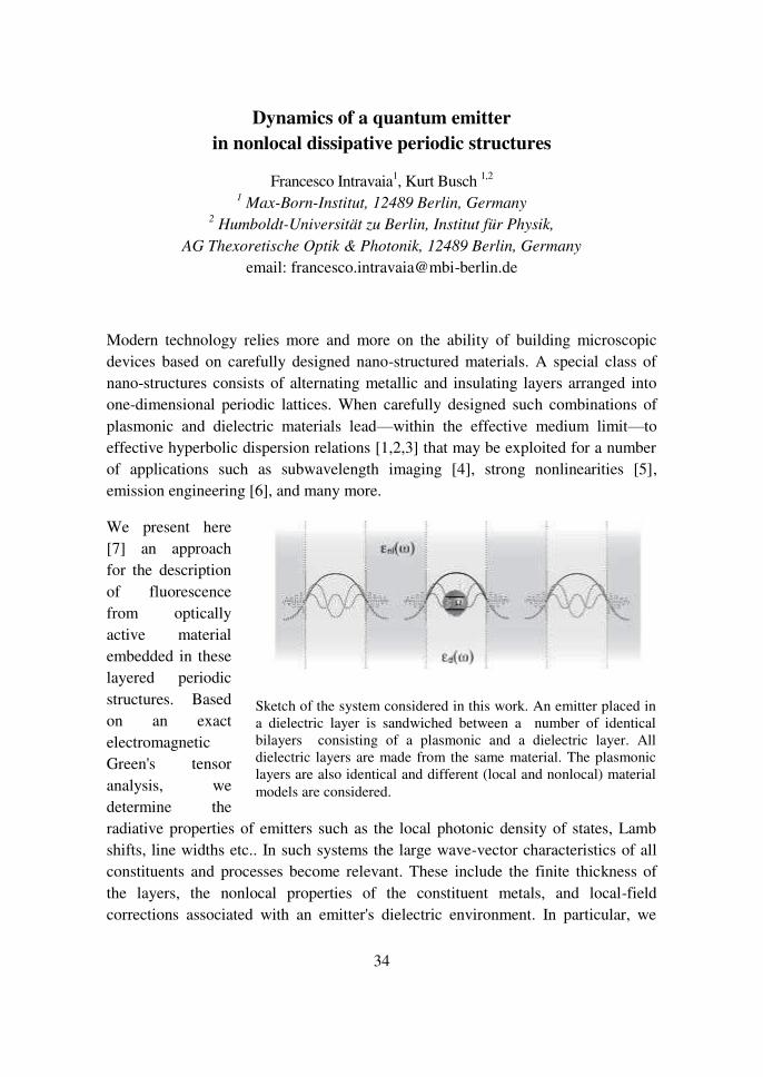
34
Dynamics of a quantum emitter
in nonlocal dissipative periodic structures
Francesco Intravaia1, Kurt Busch
1,2
1 Max-Born-Institut, 12489 Berlin, Germany 2 Humboldt-Universität zu Berlin, Institut für Physik,
AG Thexoretische Optik & Photonik, 12489 Berlin, Germany
email: [email protected]
Modern technology relies more and more on the ability of building microscopic
devices based on carefully designed nano-structured materials. A special class of
nano-structures consists of alternating metallic and insulating layers arranged into
one-dimensional periodic lattices. When carefully designed such combinations of
plasmonic and dielectric materials lead—within the effective medium limit—to
effective hyperbolic dispersion relations [1,2,3] that may be exploited for a number
of applications such as subwavelength imaging [4], strong nonlinearities [5],
emission engineering [6], and many more.
We present here
[7] an approach
for the description
of fluorescence
from optically
active material
embedded in these
layered periodic
structures. Based
on an exact
electromagnetic
Green's tensor
analysis, we
determine the
radiative properties of emitters such as the local photonic density of states, Lamb
shifts, line widths etc.. In such systems the large wave-vector characteristics of all
constituents and processes become relevant. These include the finite thickness of
the layers, the nonlocal properties of the constituent metals, and local-field
corrections associated with an emitter's dielectric environment. In particular, we
Sketch of the system considered in this work. An emitter placed in
a dielectric layer is sandwiched between a number of identical
bilayers consisting of a plasmonic and a dielectric layer. All
dielectric layers are made from the same material. The plasmonic
layers are also identical and different (local and nonlocal) material
models are considered.

35
show that the corresponding effects are non-additive and lead to considerable
modifications of an emitter's luminescence properties.
REFERENCES
[1] I. Iorsh, A. Poddubny, A. Orlov, P. Belov, and Y. S. Kivshar, Phys. Lett. A 376,
185 (2012).
[2] O. Kidwai, S. V. Zhukovsky, and J. E. Sipe, Phys. Rev. A 85, 053842 (2012).
[3] A. Poddubny, I. Iorsh, P. Belov, and Y. Kivshar, Nat Photon 7, 948 (2013).
[4] P. A. Belov and Y. Hao, Phys. Rev. B 73, 113110 (2006).
[5] G. A. Wurtz et al., Nat. Nano. 6, 107 (2011).
[6] C. L. Cortes, W. Newman, S. Molesky, and Z. Jacob, J.Optics 14, 063001
(2012).
[7] F. Intravaia and K. Busch, submitted to Phys. Rev. A 2015 (arXiv:1412.4110).
Role of collective superradiant modes on the spontaneous emission
in a dense cloud of atoms
N.J. Schilder1, C. Sauvan
1, A. Browaeys
1, J.-P. Hugonin
1 and J.-J. Greffet
1
1Institute Laboratoire C arles abry, nstitut d’ ptique, CNRS, Université Paris-Sud, 2 Avenue Augustin Fresnel, 91127 Palaiseau Cedex, France
email: [email protected]
Since the pioneering work of Dicke [1] in 1954, there has been a lot of scientific
interest in collective spontaneous emission by an ensemble of emitters. The decay
channels of these excitations correspond to eigenstates which are described by a
collective spontaneous decay rate and a collective Lamb shift, such as the super-
and subradiant states [1,2].
Although the notion of collective effects has been proposed 70 years ago, there are
still many open questions. In the original Dicke analysis, interactions between
dipoles are not included. However, when the density of emitters is high, dipole-
dipole interactions become important. In the past [2], it was thought that
superradiance breaks down in the presence of dipole-dipole interaction, as that
induces Van der Waals dephasing. In this work we have shown that superradiant
states still exist in a mesoscopic cloud of two-level systems with a very large
density, with the number of dipoles per unit volume. There exist
superradiant states which have a given oscillatory spatial structure. Furthermore, for

36
a given spatial structure, they occur at the same frequency. They are very robust in
the sense that the same structure is found for all microscopic realisations.
When atomic densities are large, one is tempted to introduce the concept of an
effective refractive index. We propose that the above-mentioned collective
superradiant modes are the most important modes for defining the effective
refractive index of the cloud. To asses this hypothesis, we compare the total field
scattered, the contribution of the superradiant modes and the field scattered by a
homogeneous particle with the atom cloud shape and an effective refractive index.
We find a very good agreement. In summary, we have found that despite the very
strong interaction, superradiant modes survive in dense media. Furthermore, these
superradiant modes are responsible for the usual scattering behaviour as described
in the standard effective medium picture. This result establishes a connection
between the collective excitation point of view of quantum optics with the
macroscopic description of electrodynamics of continuous media.
REFERENCES
[1] R.H. Dicke, Phys. Rev. 93, 1 (1954).
[2] M. Gross and S. Haroche, Physics Reports 93, 5 (1982).

37
Optical diode based on the chirality of guided photons
C. Sayrin, C. Junge, R. Mitsch, B. Albrecht, D. O'Shea,
Philipp Schneeweiss, J. Volz, A. Rauschenbeutel
TU Wien, Atominstitut & Vienna Center for Quantum Science and Technology email: [email protected]
Nanophotonic components confine light at the wavelength scale and enable the
control of the flow of light in an integrated optical environment. Such strong
confinement leads to an inherent link between the local polarization of the light and
its propagation direction [1-3], resulting in a chiral character of the light. We
employ this effect to demonstrate low-loss nonreciprocal transmission of light at the
single-photon level through a silica
nanofiber in two different
experimental schemes [4]. We
either use an ensemble of spin-
polarized atoms weakly coupled to
the nanofiber-guided mode or a
single spin-polarized atom strongly
coupled to the nanofiber via a
whispering-gallery-mode resonator.
We observe a strong imbalance
between the transmissions in
forward and backward direction of
about 10 dB for both schemes.
Remarkably, at the same time, the forward transmissions still exceeds 70 %. The
resulting optical isolator exemplifies a new class of nanophotonic devices based on
the chiral interaction of light and matter, where the state of individual quantum
emitters defines the directional behavior.
REFERENCES
[1] C. Junge et al., Phys. Rev. Lett. 110, 213604 (2013).
[2] R. Mitsch et al., Nature Commun. 5:5713 (2014).
[3] J. Petersen et al., Science 346, 67 (2014).
[4] C. Sayrin et al., arXiv:1502.01549 (2015).
Optical diode exploiting the inherent link
between the local polarization and
propagation direction of guided light.

38
Optomechanics, a platform for nanoscale quantum optics
André Xuereb1,2
1 Department of Physics, University of Malta, Msida, Malta 2 Centre for T eoretical Atomic and Molecular P ysics, Queen’s niversity Belfast,
Belfast, United Kingdom email: [email protected]
This Action brings together a wide variety of people with very different
backgrounds. Rather than a technical talk, I will use my time to give an overview of
optomechanics, as seen through the lens of someone actively working in the field
for the last several years.
Optomechanics [1] is a thriving
field that lies at the intersection
between quantum optics and
mesoscopic physics. It ranges in
application from the very
fundamental, e.g., studying the nature of
quantum mechanics on the mesoscale, to the
very applied, e.g., building devices that can convert
classical or quantum signals between microwave and
optical frequencies. Although optomechanical devices
exist in a wide range of formats and sizes, a very promising approach [2] developed
over the last few years brings the field into the realm of nanoscale optics and
therefore closer to the central scope of this Action. In this talk I intend to briefly
introduce the basic ideas underlying the field, some of its more significant
theoretical and experimental results, and also the directions that the field is moving
in.
REFERENCES
[1] M. Aspelmeyer, T. J. Kippenberg, and F. Marquardt, Rev. Mod. Phys. 86, 1391
(2014).
[2] M. Eichenfield, J. Chan. R. M. Camacho, K. J. Vahala, and O. Painter, Nature
462, 78 (2009).

39
POSTER PRESENTATIONS

40
Evolution of 1D Airy beam propagating through
a Zeeman EIT atomic medium
Dušan Arsenović, Jelena Dimitrijević and Branislav M. Jelenković
Institute of Physics, University of Belgrade, Pregrevica 118, 11080 Belgrade, Serbia
email: [email protected]
We study propagation of the one-dimensional Airy beam [1] through the atomic
medium with electromagnetically induced transparency (EIT) [2]. Maxwell-Bloch
equations are solved numerically assuming single continuous-wave laser field
resonant to the Fg=1→Fe=0 hyperfine atomic transition of the 87
Rb D2 line.
Presence of the external magnetic field removes the degeneracy of the Zeeman
magnetic sublevels, bringing tripod-like atomic scheme. Characteristics of the Airy
beam propagation through the EIT medium, slow-light Airy wave-packets and
bullets, modulation and deflection of Airy beam, have been recently studied
analytically and numerically [3, 4].
Out study analyzes how the response of the atomic medium, with induced Zeeman
EIT coherences, influences evolution of the Airy beam propagation for different
magnetic fields, inside or out of the EIT transparency window. Results are
presented for the Airy beam intensity profile during temporal evolution and also for
the deflection of the Airy beam for various propagation distances. Modulation and
deformation of the Airy beam, different levels of absorption of the Airy beam lobs,
while propagating through the EIT medium, are analyzed through the formation and
behavior of the dark-states. Presented results suggest ways of magneto-optical
control of the Airy beam and also possible applications in optical design, optical
switching, optical information processing etc.
REFERENCES
[1] Y. Hu, G. A. Siviloglou, P. Zhang, N. K. Efremidis, D. N. Christodoulides, and
Z. Chen, in Nonlinear Photonics and Novel Optical Phenomena, pp. 1, ed. Z. Chen,
R. Morandotti, Springer (2013).
[2] E. Arimondo, in Progress in Optics, vol. 35, pp. 257, ed. E. Wolf, Elsevier
(1996).
[3] C. Hang and G. Huang, Phys. Rev. A 88 013825 (2013).
[4] F. Zhuang, J. Shen, X. Du, D. Zhao, Opt. Lett. 37(15) 3054 (2012).

41
Surface plasmons excitation in Kretschmann structure with
waveguiding, amplifying and nonlinear nanoscale cover layer
H.V. Baghdasaryan1, T.M. Knyazyan
1, T.T. Hovhannisyan
1, M. Marciniak
2,3
1State Engineering University of Armenia, Yerevan, Armenia 2National Institute of Telecommunications, Warsaw, Poland
3Kielce University of Technology, Kielce, Poland email: [email protected]
Kretschmann structure with a dielectric covering
layer of different thickness and material is analysed
numerically by the method of single expression
[1,2]. Surface plasmons excitation at angular
interrogation is studied. The relevant Kretschmann
structure with cover layer is shown in the Figure.
Thin SiO2 layer in the Kretschmann structure as a
protective cover (with a thickness of few
nanometers) is considered. Covering layer of around hundred nanometers thick
exhibits waveguiding features and its excitation is possible at angles less than the
angle of surface plasmon (SP) excitation.
Inclusion of a gain in a covering layer is analysed and compensation of intrinsic loss
in a metallic layer is discussed as well. There exists minimal value of a gain for the
loss compensation that is needed for the first waveguide-mode of a covering layer.
An influence of intensity-dependent refractive index change (i.e. optical
nonlinearity) in the cover layer on SP excitation in Kretschmann structure is
analysed. Inclusion of nonlinearity in a covering dielectric layer causes the shift of
the incident wave angle of SP excitation and bistable behaviour of the angular
dependence of the reflectance. At the fixed amplitude of intensive incident wave the
hysteresis in the reflectance was revealed, which depends on the sign of
nonlinearity. Obtained distributions of the electric field and the power flow in the
nanolayers of the considered structures permit to understand the physics of
nanoscale phenomena at SP excitation.
REFERENCES
[1] H.V. Baghdasaryan, T.M. Knyazyan. Optical and Quant. Electr. 31 1059 (1999).
[2] H.V. Baghdasaryan, T.M. Knyazyan, T.T. Hovhannisyan, M. Marciniak, Optical
and Quant. Electr. 47 3 (2015).
Geometry of the problem
z
y
2
E
x H
m ~
d m 0
1
cover layer cov

42
Cavity Quantum Electrodynamics with Quantum Dots
M.P. Bakker1, A.V. Barve
2, T. Ruitenbeek
1, W. Löffler
1 , L.A. Coldren
2, D.
Bouwmeester1,2
, and M.P. van Exter1
1Huygens-Kamerlingh Onnes Laboratory, Leiden University, The Netherlands 2 University of California Santa Barbara, Santa Barbara, USA
email: [email protected]
We study single InAs self-assembled quantum dots (Qdot) in a high-finesse optical
cavity, in the form of an oxide-apertured AlGaAs micropillar [1]. This system is
ideally suited for the generation, detection and storage of quantum states of light at
the nanoscale, which is precisely the title of workgroup 1 of the COST action
‘σanoscale Quantum τptics’. This system is ideally suited because (i) it enables
strong atom-field coupling, (ii) the Qdot frequency can be easily tuned with respect
to the cavity via electrical contacts, (iii) the cavity can be made polarization
degenerate to allow access to the polarization quantum state, and (iv) both neutral
and charge Qdots can be investigated, with different level scheme and optical
polarizations. Furthermore, these semiconductor systems can be integrated in opto-
electronic networks with many elements and all types of functionalities, including
quantum memories, quantum gates, and the potential of bosonic sampling.
The figure shows how the quantum state
of a single Qdot can completely modify
the reflectivity (top figure) and
transmittivity (bottom figure) of an
optical microcavity; the dashed curves
show the corresponding measurements
for an empty cavity for reference. This
is just one of the many measurements
that we can perform and analyze. We
have also analyzed (i) avoided crossing
of dressed Qdot and optical states, (ii)
saturation effects at an average power of
<< 1 photon in the cavity, and (iii) strong
hysteresis effect due to the collection of
charge in nearby traps. Intriguing
physics that we like to investigate further.
REFERENCES
[1] M.P. Bakker et al., Appl. Phys. Lett. 104, 151109 (2014).

43
Second Harmonic generation from ZnWO4 single crystal and
ZnWO4-ZnO composites
A. Belardini1, P. Osewski
2, E. Petronijevic
1, M. Centini
1, C. Sibilia
1, D. Pawlak
2
1Sapienza Università di Roma, Rome, Italy 2 Institute of Electronic Materials Technology, Warsaw, Poland
email: [email protected]
Zinc tungstate (ZnWO4) has been known for its advantageous photoluminescent
properties, high chemical stability and low price, and it is a promising material for
various applications including scintillators, microwave devices, fiber optical
communications, NO2 sensors etc. In this work we investigate the second order
nonlinear optical response from the ZnWO4 single crystal samples, as well as from
the two ZnWO4-ZnO eutectic composites obtained by means of micro-pulling-down
technique [1]. We measure second harmonic generation (SHG) in all the samples
even though the known center of symmetry in the ZnWO4 unit cell implies zero
conversion efficiency.
In our experiment, we use a set-up similar to
the one used in [2]. We fit the conversion
efficiency of ZnWO4 by using linear
characterization from [3] and the model of
class 2 uniaxial crystals that are also
monoclinic. SHG gives us an insight into the
orientation of optical axis of the examined
samples which is always in the surface
plane. Other nonlinear processes lead to
supercontinuum generation. We get the great
enhancement in SHG signal for the samples
with ZnO lamellas. Furthermore we are improving the fabrication process which
could lead to tailoring and further control of such interesting processes in this
relatively cheap and easy-to-fabricate material.
REFERENCES
[1] D. A. Pawlak et al, Advanced Functional Materials 20, 1116-1124 (2010).
[2] A. Belardini et al, “Second Harmonic Generation Circular Dichroism from Self-
Ordered Hybrid Plasmonic-Photonic Nanosurfaces,” Adv. τpt. Mat. 2(3): 208-213
(2014).
[3] C. J. Spengler, S. τ’Hara, “Zinc Tungstate – Some τptical Properties,” App. Optics Vol. 3, No. 9 (1964).
SHG from ZnWO4: the s output as a
function of the incidence angle α and the input polarization.

44
Composite localized modes in discretized spin-orbit-coupled Bose-
Einstein condensates
P. P. Beličev1, G. Gligorić1
, A. Maluckov1, J. Petrović1 , Lj. Hadžievski1 and B. A.
Malomed2
1P* group, Vinča nstitute of Nuclear Sciences, niversity of Belgrade, Serbia 2 Department of Physical Engineering, School of Electrical Engineering, Faculty of
Engineering, Tel Aviv University, Israel email: [email protected]
The use of ultracold quantum gases, in particular bosonic and fermionic
condensates, for simulating fundamental effects originating in condensed-matter
physics has drawn much interest [1]. One of these effects is the spin-orbit coupling
(SOC). This effect plays a major role in many phenomena and applications,
including spin and anomalous Hall effects [2], topological insulators [3], spintronics
[4], etc. In contrast to the complex picture found in solids, the experimental and
theoretical description of SOC effects in Bose-Einstein condensate (BEC) is much
simpler [5]. This has motivated our study of the impact of SOC on the
immiscibility-miscibility transition in the localized complexes in BEC, which can
emulate the phase transition between insulating and conducting states in
semiconductor. For this purpose, we introduce a discrete model for binary SO-
coupled BEC trapped in a deep one-dimensional optical lattice [6]. We consider two
different types of coupling, with spatial derivatives acting inside each species, and
between the species. Stable localized composite states of miscible and immiscible
types are found to exist for both types of coupling. We also study how the transition
between miscible and immiscible type of localized complexes depends on the SOC
strength. Particularly interesting are the applications of our model to the SOC binary
condensates built of infinitely heavy atoms and the binary BEC with effective
atomic masses which have opposite signs.
REFERENCES
[1] I. Bloch, J. Dalibard, W. Zweger, Rev. Mod. Phys. 80 885 (2008).
[2] D. Xiao, M. C. Chang, Q. Niu, Rev. Mod. Phys. 82 1959 (2010).
[3] M. Hasan, C. L. Kape, Rev. Mod. Phys. 82 3045 (2010).
[4] I. Žutić, J. Fabian, S. D. Sarma, Rev. Mod. Phys. 76 323 (2004).
[5] H. Zhai, Int. J. Mod. Phys. B 26 1230001 (2012).
[6] P. P. Beličev at al, J. Phys. B 48 065301 (2015).

45
Controlling Coherence in Epsilon-Near-Zero Metamaterials
Humeyra Caglayan1,2
1Electrical and Electronics Engineering Department, Abdullah Gul University, Kayseri, Turkey
2 Bilkent University Nanotechnology Research Center, Ankara, Turkey email: [email protected]
The extreme-parameter metamaterials, such as epsilon-near-zero (ENZ) have
attracted a great deal of attention recently. Manipulating electromagnetic waves
and fields by spatially and temporally tailoring the material parameters such as
permittivity and permeability offer unprecedented tools in the design of devices and
components. EσZ structures “stretch” the effective wavelength inside the structure and as a result physical distances in such structures, although physically large, may
behave as electrically small lengths [1, 2].
It is possible to affect the degree of coherence by spatially and temporally tailoring
the material parameters. In this talk, I am going to present how an epsilon-near-
zero (ENZ) medium may be utilized to increase the degree of coherence by
comparing the field radiated from sources randomly vibrating in air to that in an
ENZ medium.
I will present the degree of incoherence caused by randomness in the location of
electromagnetic sources and how this can be reduced and controlled by embedding
these sources in an ENZ environment. The concept will be first shown numerically
for a collection of dipoles with randomized positions. Furthermore, I will present
this phenomenon in emission of quantum sources in ENZ metastructures such as a
waveguide near its cut-off frequency. ENZ materials can open up fascinating
possibilities for extending the coherence length of emitters, leading to
unprecedented light-matter interaction with long spatial coherence length.
REFERENCES
[1] B. Edwards, A. Alu, M. Young, M. Silveirinha, and N. Engheta, "Experimental
verification of epsilon-near-zero metamaterial coupling and energy squeezing using
a microwave waveguide," Phys. Rev. Lett. 100, 033903 (2008).
[2] E. J. R. Vesseur, T. Coenen, H. Caglayan, N. Engheta, and A. Polman,
"Experimental Verification of n=0 Structures for Visible Light, " Phys. Rev. Lett.
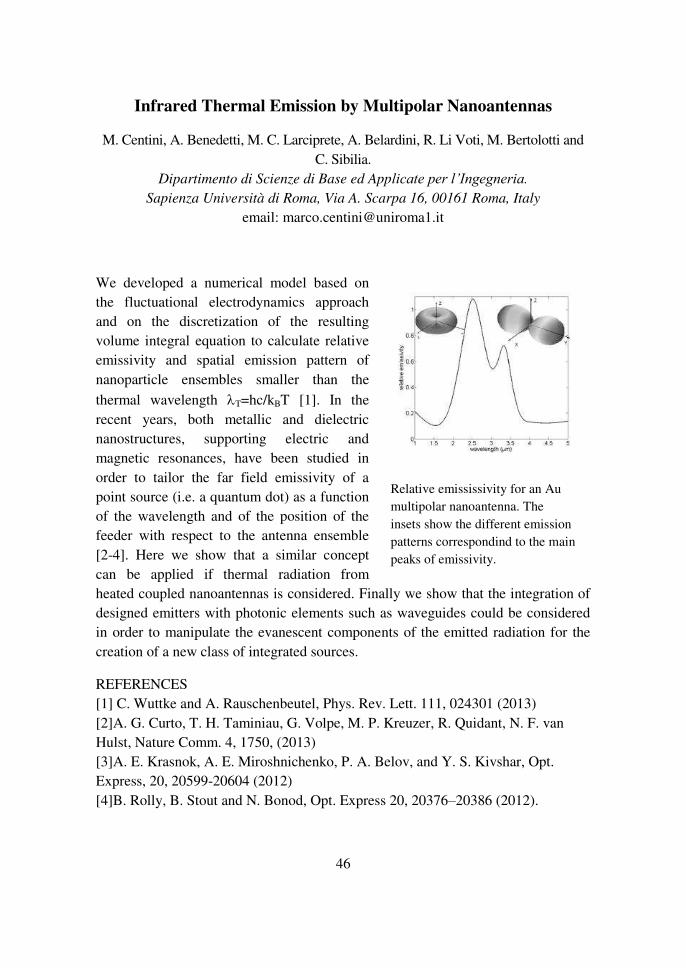
46
Infrared Thermal Emission by Multipolar Nanoantennas
M. Centini, A. Benedetti, M. C. Larciprete, A. Belardini, R. Li Voti, M. Bertolotti and
C. Sibilia.
Dipartimento di Scienze di Base ed Applicate per l’ ngegneria. Sapienza Università di Roma, Via A. Scarpa 16, 00161 Roma, Italy
email: [email protected]
We developed a numerical model based on
the fluctuational electrodynamics approach
and on the discretization of the resulting
volume integral equation to calculate relative
emissivity and spatial emission pattern of
nanoparticle ensembles smaller than the
thermal wavelength T=hc/kBT [1]. In the
recent years, both metallic and dielectric
nanostructures, supporting electric and
magnetic resonances, have been studied in
order to tailor the far field emissivity of a
point source (i.e. a quantum dot) as a function
of the wavelength and of the position of the
feeder with respect to the antenna ensemble
[2-4]. Here we show that a similar concept
can be applied if thermal radiation from
heated coupled nanoantennas is considered. Finally we show that the integration of
designed emitters with photonic elements such as waveguides could be considered
in order to manipulate the evanescent components of the emitted radiation for the
creation of a new class of integrated sources.
REFERENCES
[1] C. Wuttke and A. Rauschenbeutel, Phys. Rev. Lett. 111, 024301 (2013)
[2]A. G. Curto, T. H. Taminiau, G. Volpe, M. P. Kreuzer, R. Quidant, N. F. van
Hulst, Nature Comm. 4, 1750, (2013)
[3]A. E. Krasnok, A. E. Miroshnichenko, P. A. Belov, and Y. S. Kivshar, Opt.
Express, 20, 20599-20604 (2012)
[4]B. Rolly, B. Stout and N. Bonod, Opt. Express 20, 20376–20386 (2012).
Relative emississivity for an Au
multipolar nanoantenna. The
insets show the different emission
patterns correspondind to the main
peaks of emissivity.

47
One-dimensional sub-wavelength atom localization
via Zeeman EIT in a degenerate two-level system
Jelena Dimitrijević, Dušan Arsenović and Branislav M. Jelenković
Institute of Physics, University of Belgrade, Pregrevica 118, 11080 Belgrade, Serbia
email: [email protected]
We analyze influence of the magnetic field on the 1D atom localization [1] in an
atomic medium under the action of two optical fields, standing-wave and traveling-
wave, probe field. Optical Bloch equations are solved numerically for the Zeeman
sublevels of the hyperfine atomic transition Fg=2→Fe=1 of the 87
Rb D1 line. For
small values of the applied magnetic field, electromagnetically induced
transparency (EIT) [2] can be observed. Both fields are linearly polarized, with
mutually orthogonal polarizations and wave-vectors. Two configurations are
considered, depending whether applied magnetic field is in the direction of the
standing-wave or the probe field polarization. Information on the atom position can
be achieved both from the probe field absorption and the excited state population of
the atomic system i.e. overall lasers fluorescence.
Two presented configurations enable different transitions between Zeeman
magnetic sublevels, thus different formation of dark-states and localization patterns
i.e. atom position probability distributions within wavelength distance. Depending
on the laser fields’ intensity magnitudes and on the applied magnetic field, presented localization schemes provide variety of results. We analyze width and
contrast of the calculated localization narrow patterns for the range of laser field
intensities, both being important parameters for the experimental realization of the
localization effect. It is shown that, for the choice of parameters, magnetic field can
bring substantial changes on the behavior of the position-dependent atom–field
interaction, dark-state population, EIT and consequently localization effect. 2D
localization effect via coherent magnetic field has been recently analyzed [3] by
utilizing magnetic dipole allowed transition in a triangle atomic scheme.
REFERENCES
[1] K. T. Kapale, in Progress in Optics, vol. 58, pp. 200, ed. E. Wolf, Elsevier
(2013).
[2] S. E. Harris, Physics Today 50 36 (1997).
[3] T. Shui, Z. Wang, B. Yu, Quantum Inf. Process 14(3) 929 (2015).

48
Photonics of metal oxides: Formation of organic molecules over
their surfaces
Martin Ferus1, Svatopluk Civiš1
and Petr Kubelík1
1J. Heyrovsky Institute of Physical Chemistry, Czech Academy of Sciences, Dolejškova 3, Prague, Czec Republic
email: [email protected]
Metal oxides are well known for their photo activity. The fundamental or applied
research is therefore focused on their application in chemical synthesis, water or air
cleaning, light converting or light harvesting systems. However, one challenging
topic is focused on a little bit different problem: Their possible role in formation of
organic substances in the universe. These minerals (particularly TiO2) have been
found on Mars [1],[2] or in interstellar space [3]. Therefore, one branch of our
research deals with photonics over the metal oxides surfaces which may occur on
various stellar bodies like terrestrial planets and/or comets [4]. We have studied
several chemical reactions of inorganic molecular gases (CO2) or simple prebiotic
precursors (HCHO, HCONH2) over the TiO2 surface upon laser and broad band UV
irradiation. The reaction products were analyzed with high resolution FT absorption
spectrometry and GC-MS chromatography. The goal of this ongoing study is
to investigate the ability of the metal oxides to produce organic
molecules (hydrocarbons, sugars) under conditions of various interstellar bodies and
primordial Earth. Our newest results on photonics and photochemistry of metal
oxides show that basic prebiotic molecules (glycolaldehyde, sugars) and
hydrocarbons (methane) are formed from simple parent molecules. The research
answers fundamental questions including sugars synthesis umpolung problem or
photochemical sources of methane in atmospheres.
REFERENCES
[1] Quinn, R. C.; Zent, A. P. τrig. Life Evol. Biosph. 2λ, 5λ−72 (1λ99).
[2] Pang, K.; Ajello, J. M. Icarus 30, 63−74 (1λ77). [3] Brünken, S.; Müller, H. S.; P. Menten, K. M.; McCarthy, M. C.; Thaddeus, P.
Astrophys. J. 676, 1367−1371 (2008). [4] Ferus, M.; Civiš, S.; Šponerová, J. et al.; P.σ.A.S. 112, 657–662 (2015).
Acknowledgement: This work is a part of the research programs funded by the grant
Agency of the Czech Republic (Grant no. 14-12010S), Ministry of Education,
Youth and Sports of the Czech Republic, action COST CM1104, contract No.
LD14115 and Technological Agency of the Czech Republic (Grant No.
TA04010135).

49
Photon detectors based on High Tc Superconductors
Cheryl Feuillet-Palma1, Nicolas Bergeal
1 and Jérôme Lesueur
1
1LPEM - ESPCI/CNRS/UPMC PSL Research University, Paris (France) email: [email protected] & [email protected]
In the past years, we have been developing High-Tc Josephson nano-junctions made
by ion irradiation [1]. Based on commercial YBa2Cu3O7 thin films, this versatile
and highly scalable technique opens a new route towards superconducting
electronics in the temperature range between 20K and 80K. DC [2] and RF
applications have been explored, with very encouraging results.
In particular, we built a heterodyne
High-Tc Superconductor (HTSc)
receiver in the THz range, made of a
Josephson mixer embedded in a
broad-band antenna, operating at
50K-60K. High-frequency mixing
properties of such device up to 420
GHz has been obtained, with
interesting conversion gain [3].
Accurate modeling of the detector
was made using a three-ports model.
We now develop a new project using ion irradiation patterning of HTSc thin films.
The goal is to make HTSc Superconducting Single Photon Detectors (SSPD),
operating at higher temperature and higher speed than commercially available
SSPDs. Meander line nanowires are patterned on ultra-thin (10 to 30 nm thick)
YBa2Cu3O7 films, and polarized with a DC current close to the critical current.
Incident photons locally destroy the superconducting state, and a voltage pulse is
recorded. First DC characterization of nanowires (50 to 500 nm wide) will be
presented.
REFERENCES
[1] N. Bergeal et al. APL 87, 102502 (2005) & JAP 102, 083903 (2007)
[2] N. Bergeal et al. APL 89, 112515 (2006) & T. Wolf et al IEEE Trans. App. Sup.
23, 1101205 (2013)
[3] M. Malnou et al. APL 101, 233505 (2012) & JAP 116, 074505 (2014)
Heterodyne Josephson receiver made by
ion irradiation of HTSc

50
Proposal for an all-silicon integrated single-photon source
by unconventional photon blockade
Hugo Flayac1, Dario Gerace
2 and Vincenzo Savona
1
1 École Polytechnique Fédérale de Lausanne, Switzerland 2 Dipartimento di Fisica, Università di Pavia, Italy
email: [email protected]
Integrated single-photon sources working in the typical telecommunication band
would represent a useful building block in quantum photonics devices. Ideally, pure
single-photon states require a two-level emitter as a source. Although the recent
progress in fully integrated and telecom-compatible quantum photonics
technologies, the ability of generating single-photon states on-chip is still lacking,
owing to the lack of efficient quantum emitters at such wavelengths. As an
alternative, single-photons can be generated through the photon blockade effect, but
ordinary nonlinear materials require a large number of photons to produce
appreciable effects, owing to the intrinsically small nonlinear susceptibilities in the
bulk [1].
Here we propose an alternative all-silicon device that employs a different paradigm,
namely the interplay between quantum interference and the third-order intrinsic
nonlinearity of silicon in a system of two coupled optical cavities [2,3]. This
unconventional photon blockade allows to
produce single photons at extremely low
input power. We demonstrate how to
operate this mechanism under pulsed
optical excitation, as required for device
applications, and propose a state-of-art
implementation in a standard silicon-based
photonic crystal integrated circuit with the
smallest footprint area, as schematically
represented in the figure.
REFERENCES
[1] S. Ferretti and D. Gerace, Phys. Rev. B 85 033303 (2012).
[2] S. Ferretti, V. Savona, and D. Gerace, New J. Phys. 15 025012 (2013).
[3] H. Flayac, D. Gerace, and V. Savona, Sci. Rep. (submitted).
Representation of a single photon source
integrated in a photonic crystal platform

51
Micro-photoluminescence study of local emission of Quantum Dots
in Core-Shell GaAs/AlGaAs Nanowires
Luca Francaviglia1, Yannik Fontana
1, Gözde Tütüncüoglu
1, Federico Matteini
1, Heidi
Potts1, Sonia Conesa-Boj
1, Jordi Arbiol
2, Anna Fontcuberta i Morral
1
1Laboratoire des Materiaux Semiconducteurs, École Polytechnique Fédérale de Lausanne, Lausanne, Switzerland
2 Institut de Ciència de Materials de Barcelona, Bellaterra, CAT, Spain email: [email protected]
In the last few years quantum dots (QDs) have been shown as ideal components for
quantum photonic devices. They are excellent candidates for controlled single-
photon emitters and efficient detectors thanks to their high sensitivity to local
electric and magnetic fields. In both cases, full exploitation of QD properties can be
achieved if they are embedded in nanowires (NWs) [1]. Bright single-photon
emitters with narrow emission lines have
been recently obtained [2] by molecular
beam epitaxy as self-assembled QDs
embedded in GaAs/AlxGa(1-x)As
core/shell nanowires. They have been
studied in this work by means of large-
scale micro-photoluminescence at 14K in
order to understand the mechanisms
leading to the QD self-nucleation and
consequent growth. In particular, the QD
occurrence and emission energy in
function of the NW radial structure and
shell thickness is considered. We found
that the QD density increases with the
NW shell thickness in a non-monotonic
way. A minimum thickness threshold is necessary to observe QD emission. We
show that the deposition of an AlAs pre-deposition layer on the core facets can
lower this threshold. In addition, an overlook in the QD-size growth is given by the
evolution of the emission energy distributions. Being established on the analysis of
several hundreds of emitters, our study provides statistically valid results. SEM
investigations on fewer NWs provide a more detailed morphological insight in
agreement with the statistical outcome. These results are consistent with previous
explanations [2,3] of emission due to Ga-rich nano-formations in the AlGaAs shell.
HAADF-STEM image of a GaAs-
AlGaAs NW cross section. Zoom of
one NW corner. In the circle an Al-
poor QD is visible as a triangular
region in the shell.

52
REFERENCES
[1] J. Claudon, J. Bleuse, N. Malik, Nature Photon. 4 211117 (2010).
[2] M. Heiss, Y. Fontana, A. Gustafsson, Nat. Mater. 12 439 (2013).
[3] L. Mancini, Y. Fontana, S. Conesa-Boj, App. Phys. Lett. 105 243106 (2014).
Addressing a single photon source by a nanowaveguide
Wei Geng1, Mathieu Manceau
2, Nancy Rahbany
1, Vincent Sallet
3, Massimo De
Vittorio4, 5
, Luigi Carbone5, Quentin Glorieux
2, Alberto Bramati
2, Christophe Couteau
1,
6*
1 Laboratory of Nanotechnology, Instrumentation and Optics (LNIO), Charles Delaunay Institute, CNRS UMR 6281, University of Technology of Troyes (UTT),
10000, Troyes, France. 2 Laboratoire Kastler Brossel, CNRS UMR 8552, University Pierre and Marie
Curie, 75005 Paris, France. 3 Groupe d'étude de la matière condensée (GEMAC), CNRS, University of
Versailles St Quentin, 78035 Versailles Cedex, France. 4 Istituto Italiano di Tecnologia (IIT), Center for Bio-Molecular Nanotechnologies
Via Barsanti sn, 73010 Arnesano (Lecce), Italy. 5 National Nanotechnology Laboratory (NNL), CNR Istituto Nanoscienze, Via per
Arnesano km 5, 73100 Lecce, Italy. 6 CINTRA CNRS-Thales-NTU UMI 3288, and School of Electrical and Electronic
Engineering, Nanyang Technological University, 637553 Singapore.
The integration of single photon emitters with optical buses has recently attracted
great interests in the realm of photonic integration, as the generation and transfer of
single photons become essential in quantum information processing (QIP) [1].
Many platforms, such as photonic crystals and cavities involving complex
fabrications, have been proposed towards the collection of light from single
nanoscale emitters, while only a few of them tackle the issue of effectively
addressing a single photon emitter [2]. Herein we report a simple strategy to realise
the localised excitation of a single photon source made of a CdSe/CdS nanocrystal
using a nanowaveguide made of a single ZnO nanowire, which acts as a passive or
an active sub-wavelength nanowaveguide to excite the single photon source,
depending on whether we use above or below bandgap energy to couple light into
this nanowire waveguide. The efficient excitation of the single photon source and
the waveguiding behaviour within the nanowire in active and passive cases are

53
characterised using a photoluminescence set-up corroborated by FDTD simulations,
as well as using a Hanbury-Brown and Twiss interferometer for photon correlation
measurements. Combined with the intriguing properties of semiconductor
nanowires, such integration can be extended to various applications, for instance
electrically driven single photon emitter, efficient single photon detection and
quantum information interconnect between nodes.
REFERENCES
[1] τ’Brien, J. L.; Furusawa, A.; & Vučković, J. Photonic Quantum Technologies. Nat. Photonics 2009, 3, 687–695.
[2] Northup, T. E.; & Blatt, R. Quantum Information Transfer Using Photons. Nat. Photonics 2014, 8, 356–363.

54
Experimentally measured spectral
enhancement of NV centers vs.
distance to a planar silver mirror.
Spectral Dynamics of NV centers in the vicinity of a mirror
Niels M. Israelsen1, Jonas S. Neergaard-Nielsen
1, Ulrik L. Andersen
1 and Alexander
Huck1
1Department of Physics, Technical University of Denmark, Kongens Lyngby, Denmark
email: [email protected]
Compared to a homogeneous optical environment, the spontaneous emission rate of
a dipole emitter can be strongly modified when the emitter is placed in the vicinity
of a planar reflecting interface such as a silver mirror. Measurements of the
spontaneous emission rate as a function of emitter mirror distance can for instance
be used to determine the dipole orientation of the emitter, its internal quantum
efficiency [1], and to reveal higher order transition moments [2].
In this contribution we report on strong
modifications of the emission spectrum of
nitrogen vacancy (NV) centers placed in the
vicinity of a planar silver mirror. NV center
ensembles were prepared via nitrogen
implantation and annealing about 10 nm below
the surface of an electronic grade diamond
sample. Silver was deposited on the end facet
of a cleaved optical fiber, and the fiber was
placed with a piezo stage in the vicinity of the
diamond.
We model the vibronic spectrum of the NV center by applying the Franck-Condon
principle, and use a rate equation model to determine the spectral enhancements.
REFERENCES
[1] A. Mohtashami and A. F. Koenderink , New Journal of Physics 15, 043017
(2013).
[2] M. L. Andersen, S. Stobbe, A. S. Sørensen, P. Lodahl, Nature Physics 7, 215-
218 (2011).

55
Nonequilibrium terahertz conductivity in materials with localized
electronic states
Veljko Janković1 and Nenad Vukmirović1
1Scientific Computing Laboratory, Institute of Physics Belgrade, University of Belgrade, Pregrevica 118, 11080 Belgrade, Serbia
email: [email protected]
A broad range of disordered materials contain electronic states that are spatially
well localized. In this work [1] we studied the electrical response of such materials
to external terahertz electromagnetic field. We obtained expressions for
nonequilibrium terahertz conductivity of a material with localized electronic states
and weak electron-phonon or electron-impurity interaction. The expression is valid
for any nonequilibrium state of the electronic subsystem prior to the action of
external field. It gives nonequilibrium optical conductivity in terms of microscopic
material parameters and contains both coherences and populations of the initial
electronic subsystem's density matrix. Particularly, in the case of incoherent
nonequilibrium state of the electronic subsystem, the optical conductivity is entirely
expressed in terms of the positions of electronic states, their nonequilibrium
populations, and Fermi's golden rule transition probabilities between the states. The
same mathematical form of the expression is valid both in the case of electron-
phonon and electron-impurity interaction. Moreover, our result for the
nonequilibrium optical conductivity has the same form as the expressions
previously obtained for the case of equilibrium. Our results are expected to be valid
at sufficiently high frequencies, such that the period of the external field is much
smaller than the carrier relaxation time. We apply the derived expressions to two
model systems, a simple one-dimensional Gaussian disorder model and the model
of a realistic three-dimensional organic polymer material obtained using previously
developed multiscale methodology [2]. We note that the simple one-dimensional
model captures the essential features of the mobility spectrum of a more realistic
system. Furthermore, our simulations of the polymer material yield the same order
of magnitude of the terahertz mobility as previously reported in experiments.
REFERENCES
[1] V. Janković and σ. Vukmirović, Phys. Rev. B 90, 224201 (2014).
[2] σ. Vukmirović and L.-W. Wang, Nano Lett. 9 , 3996 (2009).

56
Controlling the emission quantum efficiency of Er3+
ions by near-
field coupling with plasmonic nanohole array
B. Kalinic1, T. Cesca
1, N. Michieli
1, C. Maurizio
1, P. Mazzoldi
1, G. Mattei
1
1 Department of Physics and Astronomy, University of Padova, Italy email: [email protected]
Due to its intense room temperature
emission at em=1.54 m, the Er3+
ion is the
main optical dopant for many
optoelectronic applications. The long
lifetime of characteristic transition 4I13/2
→4I15/2 of Er ions (about 12 ms) is one of
the major limitations in the realization of
photonic and optoeletronic devices based
on Er-doped materials, because the long
permanence of the ion in the excited state
makes it prone to non-radiative decay
processes such as energy migration,
cooperative up-conversion and
concentration quenching [1]. Since the
early work of Purcell [2], it is well known
that the variation of the local photonic
density of states can modify the
spontaneous emission rate of the emitter.
In the present work, we investigated the variation of the emission quantum
efficiency of Er3+
ions in silica layers due to the interaction at sub-wavelength
distance with Au plasmonic nanohole arrays (NHA), whose Extraordinary Optical
Transmission (EOT) peak is resonant with the Er3+
emission wavelength [3]. Time-
resolved photoluminescence (PL) measurements have shown a strong decrease of
the Er lifetime. The modification of the local density of states arising from EOT and
a resonant coupling with surface plasmon polariton modes is investigated
experimentally and by finite-element method (FEM) electrodynamic simulations.
REFERENCES
[1] E. Snoeks et al., Optical Materials 5, 159 (1996)
[2] E. M. Purcell, Phys. Rev. 69, 681 (1946)
[3] B. Kalinic et al., J. Phys. Chem. C (accepted, 2015).
(A) Variation of the Er3+ PL decay curves
at em=1540 nm as a function of the
distance from a Au NHA. (B) FEM
simulated angularly resolved power
outflow of Er emitter placed 50 nm below
a Au film and a NHA

57
Absence of mutual polariton scattering for strongly coupled surfa
ce plasmon polaritons and dye molecules with a large Stokes shift
M.A. Koponen1, U. Hohenester
2, S. Baieva
1, and J.J. Toppari
1
1Dept. of Phys., Nanoscience Center, P.O.B 35, 40014 Univ. of Jyväskylä, Finland 2Institut für Physik, Karl-Franzens-Univ., Universitätsplatz 5, 8010 Graz, Austria
email: [email protected]
During the last decades surface plasmon polaritons (SPPs) have attracted vast
interest due to promises of optics beyond the diffraction limit. Of particular interest
is also strong coupling between SPPs and molecular excitations (ME) arising from
the strongly enhanced light-matter interaction, and manifesting itself through a
formation of new SPP-ME hybrid modes exhibiting Rabi splitting even up to seve-
ral hundreds of meV [1,2]. These modes could provide the missing non-linearity to
enable interactions needed for any optical component. Also the dynamics of these
modes can differ dramatically from the dynamics of either SPP or ME, and can
significantly affect the chemical properties of the molecules involved [3].
We have demonstrated strong coupling between SPPs and various molecules [2],
and in all of them the fluorescence of MEs reveals
the coexistence of the strongly coupled polariton
modes and non-coupled MEs. As the molecular
fluorescence is directly related to the ME
occupation, it provides an ideal tool for studying
the polariton dynamics. Here we have utilized dye
molecules with an especially large Stokes shift,
i.e. Nile Red (NR), to demonstrate the absence of
scatterings among the polariton branches and to
show that the modes decay directly via dephasing
and internal relaxation of the molecules to a
fluorescing state [4]. This result provides essential
information on the dynamics of the strongly
coupled modes.
REFERENCES
[1] A.M. Glass, et al. Opt. Lett. 5, 368 (1980); J. Bellessa, et al, Phys. Rev. Lett. 9,
036404 (2004); J. Dintinger, et al. Phys. Rev. B 71, 035424 (2005); P. Vasa, et al. Nature Phot. 7, 128 (2013).
Measured fluorescence
(circles) for three NR-
samples together with the
quantum mechanical model
(solid lines)

58
[2] T.K. Hakala, et al. Phys. Rev. Lett. 103, 053602 (2009); S.V. Baieva, et al. Nanoscale Res. Lett. 7, 191 (2012); S.V. Baieva, et al. J. Chem. Phys. 138, 044707
(2013).
[3] T. Schwartz, et al. Chem. Phys. Chem. 14, 125 (2013).
[4] M.A. Koponen,e, Phys. Rev. B 88, 085425 (2013).

59
Nanostructuring of multilayered thin films by femtosecond laser
beam
Aleksander G. Kovačević1, Suzana Petrović2, Angela Beltaos, Uroš Ralević1
,
Aleksandar Matković1, Borislav Vasić1, Radoš Gajić1, and Branislav Jelenković1
1Institute of Physics, University of Belgrade 2 nstitute of Nuclear Sciences „Vinča“, niversity of Belgrade
email: [email protected]
Thin films have a wide area of application, from semiconductor technology to other
fields like optics, chemistry, mechanics: coatings for reflection/antireflection,
filtering, protection, diffusion barriers, waveguiding, sensing and decorative
purposes. Thin films can enhance
characteristics by structuring. The use of
ultrafast laser beams to generate structures
on thin films gains more and more
interest. Such interaction yields the
generation of nanoparticles which tend to
regroup on the surface and form the
structures. Nanoparticles are of great
interest due to their position between bulk
materials and atomic/molecular structures.
We have used low-fluence femtosecond
beam of various wavelegths and
expositions on thin film samples: Al on Si,
Al/Ti multilayer on Si and multilayer
graphene on SiO2. Graphene is a material
of outstanding electronic, optical, magnetic, thermal and mechanical properties, and
Al/Ti films have an important mechanical applications due to their extraordinary
wearing behavior and corrosion resistance. The exposition yielded the generation of
nanoparticles and the formation of subwavelength laser-induced periodic surface
structures (LIPSS). In Al and Al/Ti samples, preferential radius of nanoparticles
was ~25–75 nm; spatial period and width of LIPSS were ~320 nm and ~200–220
nm, respectively [1]. In graphene, preferential radius of nanoparticles was ~18 nm;
spatial period and width of LIPSS were ~70–100 and ~35 nm, respectively [2].
REFERENCES
[1] A. Kovačević, S. Petrović et al., Appl. Surf. Sci. 326 91 (2015).
[2] A. Beltaos, A. Kovačević et al., J. Appl. Phys. 116 204306 (2014).
LIPSS on multilayer grapheme.

60
High intensity broadband source of energy-entangled photons for
spectroscopy
Stefan Lerch1 and André Stefanov
1
1 Institute of Applied Physics, University of Bern, Switzerland
email: [email protected]
When pumped by a narrowband laser, photon pairs produced by spontaneous
parametric downconversion can show strong correlations in energy, i.e. the energy
of both photons from the pair sums up to the energy of the pump laser, which is
well defined. On other hand the energy of each photon from the pair can take any
value from a large spectrum, depending of the phase matching in the emission
process. Therefore broadband energy entangled photons possess simultaneously
broadband and narrowband features. It has been theoretically predicted that using
such quantum light for two-photon spectroscopy allows to reveal spectroscopic
features not accessible with classical light [1]. However no experimental
demonstration has been realized up to now because it requires a high flux of
entangled photons together with the capability to manipulate their spectrum. We are
presenting here a high flux source of highly entangled photons, pushing the creation
rate to the limit of multiple pair emission. The photon pairs are subsequently
manipulated in their energy spectrum by means of a pulse shaper, inspired from
ultrafast optics setup. In order to characterize the source and the spectral
manipulation capabilities, the photons are detected by sum frequency generation in
a non-linear crystal. This allows to study the two-photon state with femtosecond
resolution. The temporal correlation function of the two-photons can thus be
measured. Moreover the influence of dispersion on the state can be demonstrated.
Because the entanglement content of those states is intrinsically very large [2], they
are suited to study entanglement between highly dimensional states. With our setup
we demonstrated the implantation of quantum state tomography on frequency-bin
entangled qutrits and ququarts and the measurement of Bell operators as
entanglement witnesses [3]. Moreover the scheme can be extended to other
discretization procedures [4].
REFERENCES
[1] F. Schlawin, et al., Nature Communications, 4, 1782, (2013)
[2] T.P. Wihler, B. Bessire, & A. Stefanov, J. of Physics A, 47(24), 245201. (2014)
[3] C. Bernhard, B. Bessire, T. Feurer, & A. Stefanov, PRA, 88(3), 032322 (2013)
[4] B. Bessire, C. Bernhard, T. Feurer, & A. Stefanov, NJP, 16(3), 033017 (2014)

61
Single molecule fluorescence coupled to dielectric waveguides: a
new route towards integrated single photon sources
P. Lombardi,1,2
M. Maccari,3 S. Rizvi,
1 G. Mazzamuto,
1 and C. Toninelli,
1,2
G. Kewes,4 O. Neitzke,
4 A. W. Schell,
4 J. Probst,
4 J. Wolters,
4 and O. Benson
4
1European Laboratory for Non-Linear Spectroscopy (LENS), Firenze, Italy, 2INO-CNR, Istituto Nazionale di Ottica, Firenze, Italy,
3Università degli Studi di Firenze, Firenze, Italy, 4Institut für Physik, Humboldt-Universität, Berlin, Germany,
email: [email protected]
We here discuss a new kind of solid-state single-photon source based on organic
molecule emitters efficiently coupled to dielectric waveguides [1]. We investigate a
simple device consisting of single emitters (Dibenzoterrylene molecules (DBT)
hosted in anthracene crystals [2,3]) placed very close (tens of nanometers) to
dielectric Si3N4 waveguides. In this work we present a first evidence of molecules
excitation through light coupled into a waveguide.
The potentiality of this approach is also explored by means of numerical
simulations aimed at finding the optimal guiding structure for this application.
Single emitter photon coupling into a single waveguide mode up to 30% is
anticipated.
REFERENCES
[1] J. Hwang et. al, New Journal of Physics, 13, 085009 (2011)
[2] A.A.L. Nicolet et al., ChemPhysChem, 8, 1215 (2007)
[3] C. Toninelli et al., Opt. Express, 18, 7, 6577 (2010)
CCD images of one waveguide
with DBT:Ac crystal: white light
image (left) and DBT fluorescence
detection (right). Confocal laser
excitation is focused on the coupler
(red circle). The blue circle
indicates the crystal responsible for
the fluorescence (15 um apart from
the illuminated region).

62
One-dimensional superconducting photonic
crystal with dielectric defect layer
I.L. Lyubchnskii1, A.E. Zabolotin
1, N.N. Dadoenkova
1,2, Yu.S. Dadoenkova
1,2, and Y.P.
Lee3
1Donetsk Physical&Technical Institute of the National Academy of Sciences of Ukraine, Donetsk, Ukraine
2Ulyanovsk State University, Ulyanovsk, Russian Federation 3Quantum Photonic Science Research Center, Hanyang University,Seoul, Republic
of Korea email: [email protected]
Investigation of the superconducting (SC) photonic crystals (PCs) is one of
intensively developing directions in modern photonics [1]. The majority of
publications devoted to SCPC, refers to study of the ideal PCs with regular
structure. It is well known that periodicity violation leads to appearance of the
defect modes inside the photonic band gaps. In our
papers [2, 3] we investigated 1D PC with complex
defect composed of dielectric and SC layers and
showed strong dependencies of the defect mode’s intensities and positions on the thickness of SC layer
and temperature. In this communication, we present
the theoretical analysis of the spectra for the inverse
PC, namely, ternary SCPC with a dielectric defect
layer. We calculated the variation of transmitted
spectra of the SCPC of the structure
(ASB)5DB(BSA)
5, where A is strontium titanate
SrTiO3, B is aluminium oxide Al2O3, and S is high-
temperature superconductor YBa2Cu3O7. The
dependence of transmission spectra for two polarizations of light on the thickness of
SC constituent for the fixed thickness of defect layer is presented below.
REFERENCES
[1] S.M. Anlage, J. Opt. 13 024001 (2011).
[2] I.L. Lyubchanskii, N.N. Dadoenkova, A.E. Zabolotin, Y.P. Lee, and Th. Rasing,
J. Opt. A: Pure Appl. Opt. 11 114014 (2009).
[3] N.N. Dadoenkova, A.E. Zabolotin, I.L. Lyubchanskii, Y.P. Lee, and Th. Rasing,
J. Appl. Phys. 108, 093117 (2010).

63
Entanglement with negative Wigner function of 3000 atoms
heralded by a single photon
Robert McConnell1, Hao Zhang
1, Jiazhong Hu
1, Senka Ćuk1,2
and Vladan Vuletić1
1MIT-Harvard Center for Ultracold Atoms, Cambridge, Massachusetts, USA 2 Institute of Physics, University of Belgrade, Belgrade, Serbia
email: [email protected]
For measurements on N uncorrelated atoms in a coherent spin state (CSS), quantum
projection noise sets the limit of precision known as the standard quantum limit,
which scales as 1/ N . Entangled states can reduce projection noise and overcome
this limit, and are now recognized as a resource for quantum information
processing, secure communication and precision metrology. Hence an important
goal is to create the entangled states of many-particle systems while retaining the
ability to characterize the quantum state and validate entanglement. In our work we
generate entanglement of several thousand atoms by detection of a single photon
that has interacted with the ensemble. We reconstruct a negative-valued Wigner
function, an important hallmark of non-classicality, and verify an entanglement
depth of 90% atoms in the ensemble.
An ensemble of 3100 300 laser-cooled 87
Rb atoms with total spin S is confined in
an optical cavity and prepared in a CSS along x-axis, with quantization z-axis
determined by a magnetic field along the cavity. A 780-nm probe laser is coupled
into the cavity with single-atom cooperativity 1 . A single vertically-polarized
(along x) probe photon with detuning from the atomic resonance passes through
the cavity and experiences Faraday rotation. If the photon is detected with
horizontal polarization upon exiting the cavity, the atomic ensemble is projected
into non-Gaussian entangled state of collective atomic spin, i.e., the first excited
Dicke state [1] along x, which displays a negative-valued Wigner function of
0.36 0.08 and entanglement depth of 2910 190 out of 3100 atoms. This is the
first time a negative Wigner function and the mutual entanglement of virtually all
atoms have been attained in an ensemble containing more than a few particles.
REFERENCES
[1] F. T. Arecchi, E. Courtens, R. Gilmore and H. Thomas, Phys. Rev. A 6, 2211
(1972).

64
A Pulsed Nonclassical Light Source Driven by an Integrated
Electrically Triggered Quantum Dot Microlaser
P. Munnelly1, T. Heindel
1, M. M. Karow
1, S. Höfling
2, M. Kamp
2, C. Schneider
2,
and S. Reitzenstein1
1Institut für Festkörperphysik, Technische Universität Berlin, Hardenbergstraße 36, 10623 Berlin, Germany
2Technische Physik, Universität Würzburg, Am Hubland, 97074 Würzburg, Germany
email: [email protected]
The generation, manipulation, and detection of single photons on an integrated
platform is actively pursued within the nanophotonics community [1]. Linear
optics-based quantum information processing [2] and quantum cryptography
schemes [3] utilizing, e.g., the polarization of single photons, would greatly benefit
from the compactness and efficiency afforded by such architectures.
Here, we present a novel compact
nanophotonic device consisting of a
nonclassical light source excited by a
monolithically integrated and
electrically driven quantum dot (QD)
microlaser. Our device concept is
based on self-assembled InGaAs QDs
embedded in micropillar cavities.
Electrically driven micropillars act as
whispering gallery mode (WGM) microlasers operated either in continuous or
pulsed mode, with repetition rates up to 150 MHz. These microlasers are used as
on-chip excitation sources to laterally excite individual QDs in nearby micropillars,
which in turn act as vertically emitting nonclassical light sources. We demonstrate
the generation of antibunched light in continuous and pulsed operation,
demonstrating the potential of our compact solid-state platform for the generation of
triggered single photons on a highly integrated chip.
REFERENCES
[1] F. Flassig et al., arXiv:1502.05612 (2015).
[2] E. Knill, R. Laflamme, and G. J. Milburn, Nature 409, 46 (2001).
[3] N. Gisin et al., Rev. Mod. Phys. 74, 145 (2002).
Schematic of the device, showing the peripheral
target micropillar which is laterally excited by
an electrically triggered WGM microlaser.

65
Wavelenght filtering of the emission at 1.3 μm of a single InAs quantum dot by using a tunable fibre Bragg grating
G. Muñoz-Matutano1,2
, D. Rivas2, A. Ricchiuti
1, D. Barrera
1, C. R. Fernández-Pousa
3,
L. Seravalli4, G. Trevisi
4, P. Frigeri
4, S. Sales
1, J. Martínez-Pastor
2
1ITEAM Institute, U. Politécnica Valencia, C/Camino de Vera s/n, 46022 Valencia, Spain.
2Instituto de Ciencia de los Materiales, U. València, P.O. Box 22085, 46071 Valencia, Spain.
3Departamento de Ingeniería de Comunicaciones, Universidad Miguel Hernández, Av. Universidad s/n, E03202 Elche, Spain.
4CNR-IMEM Institute, Parco delle Scienze 37a, I-43100 Parma, Italy. email: [email protected]
We propose a novel -Photoluminescence ( -PL) characterization technique of
single Quantum Dots (QDs) based on the light filtering through a wavelength
tunable Fiber Bragg Grating (FBG)
instead of a standard monochromator [1].
The wavelength tuning capability (figure
1), together with the increased light
collection efficiency of the FBG, offer a
great advantage to study transient -PL ( -TRPL) of the different excitonic
transitions, by using conventional InGaAs
APD detectors. Along with these
operational improvements, the wavelength
tunable FBG offers an efficient, but easy
and cheap alternative characterization
tool, which could be easily integrated into
more complex signal treatment schemes,
as phase or amplitude modulators. With
the help of our set-up improvement, we
studied -TRPL from single QDs emitting
at 1.3 m (grown by MBE on metamorphic substrates [2]) at low
temperatures. The efficient FBG filtering could be used to improve the signal to
noise ratio in photon correlation experiments, and develop a more efficient single
Wavelenght filtering of the -
Photoluminescence emission from XX0
(b) and X+ (c) QD optical transitions
with Fiber Bragg Grating. Black lines
corresponds to the standard
monochromator adquisition.

66
photon collection in the telecom wavelengths (1300 – 1500 nm) with standard
InGaAs APD detectors.
In future applications, our FBG filtering method applied to the XX0-X
0 cascade
emission could be used to force the entanglement [3], and, hence to demonstrate
that our QDs can be used as a single photon emitters (preliminary results of HBT
experiments will be presented), or sources for polarization photon entanglement.
REFERENCES
[1] Muñoz-Matutano G, Rivas D, Ricchiuti A, Barrera D, Fernández-Pousa C R,
Martínez-Pastor J, Seravalli L, Trevisi G, Frigeri P, Sales S 2013 Nanotehcnology
25, 035204 (2013).
[2] Seravalli L, Trevisi G, Frigeri P, Rivas D, Muñoz-Matutano G, Suárez I, Alén B
and Martínez-Pastor J 2011 Appl. Phys. Lett. 98 173112
[3] Kodriano Y, Poem E, Lindner N H, Tradonsky C, Gerardot B D, Petroff P M,
Avron J E and Gershoni D 2010 Phys. Rev. B 82 155329
67
Propagation of Raman–Ramsey pulses through Rb buffer gas cell
under condition of Zeeman Electromagnetically Induced
Transparency
S. N. Nikolić1, M. Radonjić1, σ. M. Lučić1, A. J. Krmpot
1, and B.M. Jelenković1
1Institute of Physics, University of Belgrade, Serbia email: [email protected]
Experimental and theoretical investigation of time development of Zeeman
electromagnetically induced transparency (EIT) [1] during propagation of two time
separated polarization laser pulses through Rb vapour is presented [2,3]. The laser
pulses were produced by modifying laser intensity and degree of elliptical
polarization. The single laser beam is frequency locked to the hyperfine Fg=2 → Fe=1 transition of the D1 line in
87Rb.
Transients in the intensity of the − component of the transmitted light are both
measured and calculated at different values of the external magnetic field, during
the first (preparatory) and the second (probe) pulse. Zeeman EIT resonance at a
particular time instant of the pulse propagation is reconstructed by taking
normalized − transmissions at various magnetic fields at given time. From these
results, the dependence of EIT line shapes, amplitudes and linewidths on the laser
intensity, Ramsey sequence and the Rb cell temperature are examined.
It is shown that at early times of the probe pulse propagation, several Ramsey
fringes are present in EIT resonances, while at later moments a single narrow peak
prevails. Time development of EIT amplitudes are determined by the transmitted
intensity of the − component during the pulse propagation.
REFERENCES
[1] M. Fleischhauer, A. Imamoğlu, and J.P. Marangos, Rev. Mod. Phys. 77 633
(2005).
[2] S. N. Nikolić, M. Radonjić, σ. M. Lučić, A. J. Krmpot, and B.M. Jelenković, J.
Phys. B: At. Mol. Opt. Phys. 48 045501 (2015).
[3] I. Yoshida, N. Hayashi, K. Fujita, S. Taniguchi, Y. Hoshina, and M. Mitsunaga,
Phys. Rev. A 87 023836 (2013).

68
Propagation and survival of frequency-bin entangled photons in
metallic nanostructures
Laurent Olislager,1 Branko Kolaric,
2, Wakana Kubo,
3 Takuo Tanaka,
3 Renaud A. L. Vall e 4, Philippe Emplit,
1 and Serge Massar
5
1 P RA–P otonique, niversit libre de Bru elles, B-1050 Brussels, Belgium, 2Research Center in Physics of Matter and Radiation (PMR), Department of Physics, University of Namur, 61 rue de Bruxelles, B-5000 Namur, Belgium,
3Riken, Tanaka Metamaterials Lab, Japan, 4CNRS, University Bordeaux, CRPP, UPR 8641, 115 av. Schweitzer, F-33600
Pessac, France, 5Laboratoire d’ nformation Quantique, niversit libre de Bru elles, B-1050
Brussels, Belgium email: [email protected]
Here we present an analysis of interactions of frequency-bin entangled photons with
different plasmo- photonic nanostructures i.e. a nanosphere (HPPS) array and a
nanopillar (NPA) array respectively. Specifically, in this study we address two
pivotal questions. First, in which cases and to what extent does frequency-bin
entanglement survive when a photon
is subject to a plasmonic conversion?
Second, could the nature of a
resonance affect the coherence of the
photon-plasmon-photon conversion
process? Figure a shows typical
results performed on our structures.
Experimental measurements
extracted from coincidence peaks
(Figure b) are in good agreement
with the predictions. After
subtraction of the background noise,
large net visibilities are obtained. In
conclusion, we find no evidence for decrease of coherence when photons are
converted to mesoscopic electronic excitations. Indeed the only parameter that
seems to influence the results are the losses of the samples, which are much higher
for a flat gold film than for the investigated plasmonic structures due to the
existence of plasmonic resonances.

69
Imaginary and real part of
susceptibility vs. probe field
detuning with R0=8 a.u.* and
B0=0.5 a.u.* .
Electromagnetically induced transparency in spherical quantum
dot with on-center hydrogen impurity in magnetic field
V. Pavlović and Lj. Stevanović
Faculty of Science and Mathematics, University of Nis email: [email protected]
Electromagnetically induced transparency (EIT) is an atomic coherent effect that
permits propagation of electromagnetic radiation without attenuation through
otherwise opaque medium [1]. In recent years, this phenomenon has been
investigated in nanostructures such as semi-
conductor quantum wells and quantum dots
(QD) due to their practical applications (e.g. in
telecommunications, optoelectronic devices,
EIT-based quantum memories) [2 - 4].
In this paper we have analyzed the realization
of EIT with hydrogenic impurity located in the
center of 3D spherical QD in the presence of
static magnetic field at intermediate strength.
The energy levels of impurity 1s0, 2p-1 and 3d-2,
which are included in consideration, together
with probe and control laser fields, inducing -
transitions, form a ladder-type three-level atom.
The optical Bloch equations in steady-state
regime are solved and it is discussed
dependence of the susceptibility on the QD
radius R0, Rabi frequency of coupled field ΩC,
detuning of the probe field ∆p and magnetic
field strength B0.
REFERENCES
[1] K. -J. Boller, A. Imamoğlu, S. E. Harris, Phys. Rev. Lett. 66 2593 (1991).
[2] Z. Raki, H. R. Askari, Superlattices and Microstruct. 65 161 (2014).
[3] G. Rezaei, S. Shojaeian Kish, B. Vaseghi, S. F. Taghizadeh, Phys. E 62 104
(2014).
[4] P. Kaer Nielsen, H. Thyrrestrup, J. Mørk, B. Tromborg, Opt. Express 15 6396
(2007).

70
Perforated SOI Microring Resonators for Enhanced Light Matter
Interaction
Raimondas Petruškevičius1, Darius Urbonas
1, Martynas Gabalis
1, Konstantinas
Vaškevičius1, Armandas Balčytis1,2
, Saulius Juodkazis2
1Center for P ysical Sciences and Tec nology, Savanorių ave. 23 , Vilnius LT-02300, Lithuania
2Centre for Micro-Photonics, Swinburne University of Technology, Hawthorn, VIC 3122, Australia
email: [email protected]
A novel perforated microring resonator structure with low relative permittivity
material defects has been proposed for enhancement of light matter interaction,
sensing and applications in nanoscale quantum optics. The device fabricated on a
Silicon-on-Insulator (SOI) platform. We present numerical simulations of the
perforated optical microring resonator based finite-difference time domain (FDTD)
and finite-element methods (FEM). The bottlenecks of simulation time for FDTD
method were resolved by harnessing graphical processing unit (GPU) computation
techniques. It was shown that GPU based FDTD implementation performs the same
simulation task up to 18 times faster.
The performance in enhancement of light matter interaction of perforated microring
resonator in bulk and surface sensing schemes has been analyzed. We show that our
proposed refractive index sensor based on a modified microring resonator
significantly outperforms ordinary microring resonators. The presented perforated
microring resonator allows for variation of both, the quality factor and the
sensitivity, making it applicable in many optical applications. Our design not only
achieves high sensitivity, but also increases the total area of the interface between
the microring resonator and the surrounding medium, which enhances the light
matter interaction, and has high potential in nanoscale quantum optics applications.
The initial device fabrication results are discussed. It is shown that microring
resonator with sub wavelength perforations enhances SOI ring sensor sensitivity 3-5
times. The microring resonator with a first order Bragg grating and a defect mode
has large spatial detection resolution and wider free spectral range (FSR). On the
other hand, if the microring is modified with a second order Bragg grating, the
resulting structure can be used for vortex sensors and micro-manipulation of
particles.

71
Different strategies towards the deterministic coupling of a Single
Quantum Dot to a Photonic Crystal Cavity Mode
I.Prieto1, J.Herranz
1, Y.González
1, P.A.Postigo
1*, B.Alén
1, L.González
1,
J.Martín‐Sánchez1, L.J.Martínez
1, M.Kaldirim
1, D. Fuster
2, J.Canet‐Ferrer
2,
G.Muñoz‐Matutano2, and J.Martínez‐Pastor
2
1 IMM-Instituto de Microelectrónica de Madrid (CNM-CSIC), Isaac Newton 8, PTM, E-28760 Tres Cantos, Madrid, Spain
2 UMDO (Unidad Asociada al CSIC-IMM), Instituto de Ciencia de Materiales, Universidad de Valencia, P.O. Box 22085, 4607 Valencia, Spain
email: [email protected]
In this work we present two strategies for coupling of InAs site-controlled QD
with the mode of GaAs- based PC nanocavities. In both approaches InAs QD are
formed at specific sites of the GaAs surface defined by the presence of
nanoholes formed after desorption of the GaAs oxide points obtained by AFM local
oxidation lithography. These site-controlled nanostructures show good optical
emission properties and are efficient quantum emitters operating as single photon
sources. In both approaches the photonic crystal nanocavities are fabricated by e-
beam lithography and dry etching on GaAs epitaxial layers grown by molecular
beam epitaxy.
Site controlled InAs QD fabrication at the maximum of the electric field of a pre-
patterned photonic crystal cavity. (a) Fabrication of the photonic crystal structure and
GaAs oxide dot (AFM local oxidation); (b) The structure is completed by a regrowth
process up to 140nm thickness with an embedded site-controlled InAs QD placed 20nm
below the surface.
72
Polaron transport in nanocrystal solids
σikola Prodanović1, σenad Vukmirović1
1Scientific Computing Laboratory, Institute of Physics Belgrade, Serbia email: [email protected]
Colloidal quantum dot supercrystals are novel nanostructured materials which
appear very promising in potential optoelectronic applications and for fundamental
study of electronic transport properties in condensed matter physics. Recent
fabrication of high quality supercrystals with relatively strong inter-site electronic
coupling and high size monodispersity enabled high carrier mobilities that slightly
increase with decreasing temperature. Due to such temperature behaviour it is
believed that such transport is so called coherent band-like transport.
We developed an accurate model accounting for electron-phonon interaction in
colloidal quantum dot supercrystals that allowed us to identify the nature of charge
carriers and the electrical transport regime. We find that in experimentally relevant
CdSe nanocrystal solids the electron-phonon interaction is sufficiently strong that
small polarons localized to single dots are formed. Charge-carrier transport occurs
by small polaron hopping between the dots with mobility that decreases with
increasing the temperature. While such a temperature dependence of mobility is
usually considered as a proof of band transport, we show that the same type of
dependence occurs in the system where transport occurs by small polaron hopping.
REFERENCES
[1] σ. Prodanović, σ. Vukmirović, Z. Ikonić, P. Harrison, and D. Indjin, J. Phys. Chem. Lett. 5, 1335 (2014).

73
Directional couplers based on open and closed waveguide arrays
Ana Radosavljević, Jovana Petrovic, Aleksandar Daničić, Aleksandra Maluckov and Ljupčo Hadžievski
P⋆Group, Vinča nstitute of Nuclear Sciences, niversity of Belgrade, P. .B. 522, Belgrade, Serbia
email: [email protected]
Multiport optical couplers are of great interest as interferometric beam splitters in
quantum optics and sensing [1]. They are realized by concatenating or nesting
single-mode two-port couplers, or by using multimode interference. Here, we
propose alternative multiport optical couplers based on open and closed finite
waveguide arrays in two compact architectures: planar waveguide arrays (WGA)
and circular multicore fibers (MCF). Directional coupling is based on periodic
energy exchange between waveguides achieved by engineering their coupling
coefficients to yield the eigenvalues of the system coupling matrix commensurable.
a) WGA, b) MCF, c) an example of periodic energy transfer in a realistic 5-guide open
array.
Equal coupling coefficients render periodic propagation dynamics in the case of
M=2,3 for WGA and M=2,3,4,6 for the circular array, where M is the number of
cores. Starting from the eigenvalue commensurability condition, we derive ratios
between the coupling coefficients that render periodicity for M=4,5 WGAs, [2]. We
also consider adding the central core to the MCF and derive an additional condition
for the coupling coefficients that should be fulfilled to achieve periodic dynamics.
We use these findings to design 1x2, 1x4 and binomial directional couplers. They
are of interest for optical circuits, multipath interferometers and coherent energy
transport. The results are corroborated by numerical simulations of realistic WGAs.
REFERENCES
[1] B. J. Metcalf et al., Nat. Commun. 4 1356 (2013).
[2] J. Petrovic, Opt. Lett. 40 139-142 (2015).

74
Operating Quantum Dot Single-Photon Sources
Using a Compact Stirling Cryocooler
A. Schlehahn, M. Gschrey, J.-H. Schulze, S. Rodt, A. Strittmatter, T. Heindel,
and S. Reitzenstein
Institut für Festkörperphysik, Technische Universität Berlin, Hardenbergstraße 36, 10623 Berlin, Germany
email: [email protected]
The emerging field of quantum information technology has become a major driving
force for the development of easy-to-operate single-photon sources (SPSs) [1] and
detectors [2]. To realize practical solid state based SPSs, mainly two different routes
can be pursued: first, specific materials can be used to achieve room temperature
operation, and second, an easy-to-handle cooling technique can be applied to
operate readily available high-quality single-photon emitters at cryogenic
temperatures.
Here, we report on the application of a
compact and user-friendly Stirling
cryocooler (c.f. Figure inset) in the field
of nanophotonics. The Stirling
cryocooler is used to operate a single
quantum emitter constituted of a
semiconductor quantum dot (QD) at a
temperature of (28.79 0.07) K [3].
Proper vibration decoupling of the
cryocooler and its surrounding enables
free-space micro-photoluminescence
spectroscopy to identify and analyze
different charge-carrier states of a
single quantum dot. As an exemplary application in quantum optics, we perform
Hanbury-Brown and Twiss experiments demonstrating a strong suppression of
multi-photon emission events with g(2)
(0) < 0.04 from this Stirling-cooled single
quantum emitter (c.f. Figure).
REFERENCES
[1] G.-C. Shan, Z.-Q. Yin, C.-H. Shek, and W. Huang, Front. Phys. 9, 170 (2014).
[2] R. H. Hadfield, Nat. Photonics 3, 696 (2009).
[3] A. Schlehahn et al., Rev. Sci. Instrum. 86, 013113 (2015).
Photon-autocorrelation measurement of a
single quantum dot operated with a plug-
and-play Stirling cryocooler (see inset).

75
White light generation and non-linear optical properties of Ag
nanoclusters and nanoparticles dispersed in the glass host
Mikhail V. Shestakov1, Vladimir E. Kaydashev
1,2, Hong Hanh Mai
1,2, Ewald
Janssens2, Maria Meledina
3, Stuart Turner
3, Peter Lievens
2, Gustaaf Van Tendeloo
3 and
Victor V. Moshchalkov1
1INPAC-Institute of Physics and Chemistry, KULeuven, B-3001 Leuven, Belgium 2 Laboratory of Solid State Physics and Magnetism, KULeuven, B-3001 Leuven,
Belgium 3 EMAT, Department of Physics, University of Antwerp, 2020 Antwerp, Belgium
email: [email protected]
Ag- doped bulk oxyfluoride glasses have been prepared by conventional melt-
quenching method. The photoluminescence excitation and emission spectra of the
as-prepared glass cover wide range from 300 to 500 nm and from 400 to 900 nm,
respectively, corresponding to the typical spectra of Ag nanoclusters with size less
than 1.2 nm [1, 2]. The particular preparation conditions result in a glass with white
light luminescence based solely on emission of Ag nanoclusters under excitation in
UV [3]. Likewise, the white light generation may be achieved via co-doping with
Tm3+
ions emitting in the blue region [4]. The quantum yield of the prepared glasses
was found to be up to 70% [1]. The as-prepared glasses were heat-treated at 350 oC
(below glass transition temperature) preserving glassy state of the samples. Under
heat-treatment the Ag nanoclusters coalesce into the amorphous nanoparticles larger
than 2 nm exhibiting a broad surface plasmon absorption band centered at 480 nm
in the visible range. These amorphous Ag nanoparticles do not emit light due to the
ascribing plasmonic properties. Open aperture z-scan experiments were conducted
using 480 nm nanosecond laser pulses. These experiments revealed that the Ag
nanoclusters and nanoparticles exhibit non-saturated and saturated non-linear
absorption with large non-linear absorption indices, respectively [5]. The prepared
glasses may be applied for white light generation under UV excitation, optical
limiting and object’s contrast enhancement.
REFERENCES
[1] A. S. Kuznetsov, V. K. Tikhomirov, M. V. Shestakov and V. V. Moshchalkov,
Nanoscale 5 10065 (2013)
[2] V. K. Tikhomirov, T. Vosch, E. Fron, V. D. Rodríguez, J. J. Velázquez, D.
Kirilenko, G. Van Tendeloo, J. Hofkens, M. Van der Auweraer, V. V.
Moshchalkov, RSC adv. 2 1496 (2012)
[3] A.S. Kuznetsov, V.K.Tikhomirov, V.V.Moshchalkov, Mater. Lett. 92 4 (2013)

76
[4] M.V. Shestakov, X.M. Chen, V. Kaydashev, W. Baeckelant, V.K. Tikhomirov,
J.Vanacken, J. Hofkens, V.V. Moshchalkov, Opt. Mat. Express 4 1227 (2014)
[5] H.H. Mai, V.E. Kaydashev, V.K. Tikhomirov, E. Janssens, M.V. Shestakov, M.
Meledina, S. Turner, G. Van Tendeloo, V.V. Moshchalkov, P. Lievens, J. Phys.
Chem. C 118 15995 (2014)

77
Slow-Light Metamaterials
Philippe Tassin
Chalmers University of Technology
I will discuss the state-of-the-art in slow-light metamaterials [1], i.e., effective
media in which light propagates at a group velocity much smaller than the speed of
light in vacuum. Slow-light metamaterials are based on a classical analogue of
electromagnetically induced transparency.
The metamaterials consists of a radiative
meta-atom coupled by near fields to a dark
meta-atom that traps the optical energy [2-3].
Two important aspects of slow-light
metamaterials will be discussed: the design
of the dark meta- atom (minimizing radiation
loss) and the choice of material
(minimizing dissipative loss) [4]. This will
culminate in our latest designs based on
dielectric metamaterials excited by
nonresonant antennae [5].
REFERENCES
[1] P. Tassin, T. Koschny, C. M. Soukoulis, Classical Analog of
Electromagnetically Induced Transparency in Metamaterials and Wave Control, Wiley (2013).
[2] P. Tassin, L. Zhang, T. Koschny, E. N. Economou, C. M. Soukoulis, Phys. Rev.
Lett. 102, 053901 (2009).
[3] P. Tassin, L. Zhang, T. Koschny, E. N. Economou, C. M. Soukoulis, Opt.
Express 17, 5595 (2009).
[4] C. Kurter, P. Tassin, L. Zhang, T. Koschny, S. M. Anlage, C. M. Soukoulis,
Phys. Rev. Lett. 107, 043901 (2011).
[5] A. Jain, P. Tassin, T. Koschny, C. M. Soukoulis, Phys. Rev. Lett. 112, 117403
(2014).
Design of a slow-light metamaterial.

78
Bright Emission of Indistinguishable Photons from
Deterministically Fabricated Quantum Dot Microlenses
A. Thoma1, P. Schnauber
1, M. Gschrey
1, R. Schmidt
1, B. Wohlfeil
2, M. Seifried
1, J.-H.
Schulze1, S. Burger
2, F. Schmidt
2, A. Strittmatter
1, S. Rodt
1, T. Heindel
1, S.
Reitzenstein1
1Institute for Solid-State Physics, Technical University Berlin, Berlin, Germany 2 Zuse-Institute Berlin (ZIB), Berlin, Germany
email: [email protected]
Bright non-classical light sources emitting single and indistinguishable photons on
demand constitute essential building blocks towards the realization of quantum
communication networks [1]. In this work we report on efficient single photon
sources based on deterministically fabricated single quantum dot (QD) microlenses.
Close to ideal performance of the non-classical light-sources in terms of photon
extraction efficiency, high suppression of multi-photon events and a high degree of
indistinguishablility is ensured by applying in-situ electron beam lithography [2]
with high process yield of >90%.
In our concept we combine
cathodoluminescence spectroscopy with
advanced in-situ 3D electron-beam lithography
at cryogenic temperatures to pattern monolithic
microlenses precisely aligned to pre-selected
single QDs. Here, the microlenses allow for a
broadband enhancement of the extraction
efficiency, which can reach values beyond 80
% if combined with a lower Au mirror. The
quantum character of emission is tested by
photon-autocorrelation measurements and
reveals very high suppression of multi-photon
emission events with g(2) τ ≤0.01 even for optical pump powers of two times the
saturation power (cf. Figure). Moreover,
performing Hong-Ou-Mandel experiments
under pulsed p-shell excitation allows us to
demonstrate an interference visibility exceeding 80 %, which reveals a very high
degree of indistinguishability of the emitted photons.
Micro-photoluminescence
emission spectrum and power
dependent photon-
autocorrelation measure-ments
of a QD microlens (cf. inset).
79
REFERENCES
[1] N. Gisin, R. Thew, Nat. Photonics 1, 165 (2007).
[2] M. Gschrey et al., Appl. Phys. Lett. 102, 251113 (2013)
Azophenylcarbazoles: isomerization and application to
functionalize GaN surface.
R.Tomašiūnas1, A.Balčytis1, G.Seniutinas
1, V.Bikbajevas
1, R.Petruškevičius2,
V.Getautis3
1Institute of Applied Research, Vilnius University, Sauletekio 10, 10223 Vilnius, Lithuania
2Center for Physical Sciences and Technology, Savanorių 23 , 02300 Vilnius, Lithuania
3Kaunas niversity of Tec nology, Radvilėnų 9, 27 Kaunas, Lit uania
If a material with initial centrosymmetric structure irradiated with fundamental
and its second harmonic 2 beams is able to absorb these beams, quantum
interference between two photons and one 2 photon to same energy level can be
achieved. Thus depending on phase difference between these two beams poling
electric field inside the material can be created. Such oriented distribution makes
molecules bleached out towards direction of the electric field polarization. This
induced molecular orientation breaks the initial centrosymmetric structure inside
material creating quasi-phase-matched grating of nonlinear second-order
susceptibility (2) applicable to second harmonic generation. That’s the basis for all-
optical poling – a method used to investigate optical storage materials. Key point
for optical storage application is to fix molecules oriented in the host matrix. To be
successful one needs to overcome problems like photoinduced (reading) and
thermally driven relaxation. Increase of the first leads to a dramatic “wash-out” of the non-centrosymmetry [1]. Temperature measurements were performed to
investigate thermoisomerization phenomena. For azophenylcarbazoles in
polycarbonate a model describing all-optical poling transients using an approach of
three relaxation rates was applied to interpret the experimental results measured in a
wide range of temperatures 300 K–150 K, thus covering the β transition for the host [2]. The rates for thermoisomerization (10
−5–10−2
s−1
) and for orientational diffusion
of trans isomer (10−6–10
−4 s
−1) exhibited diverse temperature dependent behavior
manifesting non-Arrhenius type dependence for the highest rate interpreted using a
geometry ”adjustment” model. At temperatures far below Tg we were able to

80
uncover the situation when the orientational randomization is suppressed
considering the azochromophores as “frozen”. Highest values of (2) (0.72 pm/V)
and lowest mobility were obtained for the most branched azophenylcarbazoles [3].
To enhance the interaction with host matrix genuine molecular glasses were
investigated [4].
Combined with the prominent optoelectronic material GaN the fascinating
isomerization properties of azochromophores may provide a great potential for
developing hybrid multifunctional devices. Smart surfaces and interfaces are the
basis for sensors and FETs. Our interest extended towards azochromophore self-
assembled monolayers (SAM) on GaN. By means of surface hydroxylation
assemblies of azophenylcarbazole molecules were chemisorbed and aligned in
closely-packed SAMs on GaN due to intermolecular forces. Since self-assembly
and homogeneity of coverage of gallium nitride surface by azochromophores aren’t simple tasks, several configurations of surface active headgroups have been tested.
Wetting behavior, XPS and work function investigations provided indication that
GaN surface was successfully functionalized by azophenylcarbazole SAMs [5].
Modulation of gallium nitride work function via resonantly photoinduced trans→cis
isomerization confirmed the latter process. Depending on the molecule architecture
the attachment quality was predicted and the results will be discussed.
REFERENCES
[1] G.σavickaitė et al. Phys. Status Solidi A 208(8), 1833(2011).
[2] G.Seniutinas et al. Phys. Chem. Chem. Phys. 15, 14219(2013).
[3] G.σavickaitė et al. Dyes and Pigments 92, 1204(2012).
[4] G.Seniutinas et al. Mol. Cryst. Liq. Cryst. 556, 124(2012).
[5] V.Bikbajevas et al. Mol. Cryst. Liq. Cryst. 604, 52(2014).

81
Metamorphic InAs/InGaAs nanostructures
for single QD emission in the telecom range
Giovanna Trevisia, Luca Seravalli
a, Guillermo Muñoz-Matutano
c, David Rivas
b, Juan
Martinez-Pastorb and Paola Frigeri
a
aIMEM-CNR, Parco Area delle Scienze, 37/a, I-43100 Parma, Italy bInstituto de Ciencia de los Materiales, Universitat de València, 46071 Valencia,
Spain cOptics and Quantum Comunications group, ITEAM, UPV, Valencia, Spain.
email: [email protected]
InAs self-assembled semiconductor quantum dots (QDs) can be viable sources of
single photons, but strong research efforts are still needed to engineer the structure
to tune the emission in the telecom window (1.3 - 1.55 µm). [1]
We present the design, the MBE growth and the optical characterization of
metamorphic InAs/InxGa1-xAs QDs with a density low enough for single QD
characterization. [2] The MBE growth is based on the deposition of InAs sub-
critical coverages on InxGa1-xAs metamorphic buffers (MBs): QD emission is
redshifted due to the reduction of QD strain and QD-MB band discontinuities, as
verified by model calculation carried on with the Tibercad software. [3]
Optical properties were studied by
ensemble PL at 10K and by µ-PL
at 4K and single QD emission was
detected from 1000 to 1315 nm:
most of the excitonic species at the
ground state were detected. In
conclusion, our results show that
metamorphic InAs/InGaAs QDs
can be effective single photon
sources emitting at 1.3 - 1.55 µm
at low temperature.
REFERENCES
[1] C.L. Salter, R.M. Stevenson,
I. Farrer, C.A. Nicoll, D.A. Ritchie, and A.J. Shields, Nature 465, 594 (2010).
[2] L. Seravalli, G. Trevisi, and P. Frigeri, CrystEngComm 14, 6833 (2012).
[3] www.tiberlab.com
[4] L. Seravalli, G. Trevisi, P. Frigeri, D. Rivas, G. Munoz-Matutano, I. Suarez, B.
Alen, J. Canet, and J.P. Martinez-Pastor, Appl. Phys. Lett. 98, 173112 (2011).
µPL QD spectra from QDs on In0.15Ga0.85As MBs

82
Progress in the fabrication of open-access microcavities using
focused ion beam milled substrates
Aurélien Trichet, Sam Johnson, Philip Dolan and Jason Smith
Department of Materials, University of Oxford, UK email: [email protected]
Open access microcavities have become popular in recent years for cavity QED of
both atomic and solid state systems, due to their ready tunability, ease of access to
the confined cavity mode, as well as high finesses and small mode volumes. A
number of techniques have
been used to fabricate the
concave substrates of such
cavities including chemical
etching [1], laser processing
[2], and focused ion beam
milling [3]. This latter method
has the advantage of offering
precision shapes at length
scales much shorter than the
optical wavelength, thereby
offering the smallest mode
volumes and ready engineering
of new structures such as
coupled cavities, whilst
providing finesse comparable
with the best of other methods.
We will present some of the latest developments in the fabrication of cavities using
focused ion beam methods, along with some recent work on coupling of emitters
such as single nitrogen-vacancy centres in diamond to cavity modes.
REFERENCES
[1] M. Trupke, E. A. Hinds, S. Eriksson, E. A. Curtis, Z. Moktadir, E. Kukharenka,
and M. Kraft, Appl. Phys. Lett. 87, 211106 (2005).
[2] D. Hunger, T. Steinmetz, Y. colombe, C. Deutsch, T. W. Hänsch and J. Reichel,
New J. Phys. 12, 065038 (2010)
[3] P. R. Dolan, G. M. Hughes, F. Grazioso, B. R. Patton, and J. M. Smith, Optics
Lett. 35, 3556 (2010)
SEM micrographs of FIB milled substrates; cross
sectional micrograph of a 7 m radius of curvature
substrate with DBR coating; and transmission
spectrum of a high finesse cavity.

83
Near-Field Optical Detection of Plasmon Resonances
C. Triolo1, S. Trusso
2, S.Patanè
1, S. Savasta
1 and R.Saija
1
1 Dipartimento di Fisica & Scienze della Terra, University of Messina, Italy 2CNR-IPCF, Istituto per i Processi Chimico-Fisici, Messina
email: [email protected]
The plasmons properties depend on many factors, such as composition, size, shape
and arrangement of nanoparticles. In this talk, we propose a method to obtain an
indirect precise measure of the nanoparticle dimension from the backscattering. The
method basically consists in excite the plasmon resonance by means of a near field
aperture probe collecting in the far field the interference arising from the incident
field and the superimposed scattered one. The interaction between the incident and
the scattered field in backscattering zone as a function of tip–sample distance has
been resorting to multipolar expansion of of the fields and on T-matrix approach[1].
To validate the model we studied the optical properties of gold nanoparticles
deposited by pulsed laser ablation [2] and investigated by near-field optical
microscopy (SNOM) in a transmission far-field collection scheme [3]. The
theoretical model almost accurately reproduces the experimental data and makes us
confident that the used method is suitable to describe more complex systems of
metal nanoparticles.
REFERENCES
[1] Borghese F, Denti P, Saija R (2007) Scattering from model nonspherical
particles. Springer, Berlin Heidelberg
[2] C. D’Andrea, F. σeri, PM τssi, σ Santo, S. Trusso,. σanotechnology, 20:245606 (2009).
[3] E. Cefalì, S. Patanè, PG Gucciardi, M. Labardi,M. Allegrini, J Microscopy 210,
262 (2007)

84
Quantum Communications along free-space and satellite channels:
a workbench for Nanoscale Quantum Processes
Giuseppe Vallone, Daniele Dequal, Marco Tomasin, Matteo Schiavon,
and Paolo Villoresi
Quantum Future Research Group Università degli Studi di Padova – DEI
Padova, Italy email: [email protected] . WEB: quantumfuture.dei.unipd.it
Quantum Communications represent a paradigm shift with respect to classical
counterpart allows envisaging demonstrations of test of Quantum Mechanics over
planetary scale as well as protocols of Quantum Information, quantum teleportation
along satellite-to-ground or intersatellite links. The sharing of quantum states
among ground and orbiting terminal may be considered as feasible with present
optical means [1,2]. However, the extension of the Quantum Communications and
Technologies to long distances, on the surface of the Earth as well as from the Earth
to an orbiting terminal in Space, is influenced by difficulties, among which the
moving terminals, the large losses, the effects on the optical propagation of the
turbulent medium.
The development of novel scheme for quantum devices in the nanoscale for
generation, detection and storage of quantum states is expected to provide a great
impulse in the area.
To present the actual state of the research, we will present the experimental studies
on the faithful transmission of qubits from Space to ground and from distant
terminals on the Earth which demonstrates the means for realizing Space Quantum
Communications [3].
REFERENCES
[1] P. Villoresi et al., “Experimental verification of the feasibility of a quantum channel between space and Earth,” σew Journal of Physics, vol. 10, no. 3, p. 33038, 2008.
[2] A. Tomaello et al., “Link budget and background noise for satellite quantum key distribution,” Advances in Space Research, vol. 47, no. 5, pp. 802–810, 2011.
[3] G. Vallone et al., “Experimental Satellite Quantum Communications,” arXiv preprint arXiv:1406.4051, 2014.

85
Ab initio dielectric responses as a basis for computational
plasmonics and photonics
Robert Warmbier1,2,3
, Alexander Quandt1,2,3
1School of Physics, University of the Witwatersrand, Johannesburg, South Africa 2NRF-DST Centre of Excellence in Strong Materials, University of the
Witwatersrand, Johannesburg, South Africa 3Materials for Energy Research Group, University of the Witwatersrand,
Johannesburg, South Africa email: [email protected]
Theoretical simulations offer complementing insight into physical properties
compared to experimental set-ups. In the field of optics we are often confronted
with multi-scale problems. The fundamental dielectric response of a system is
determined by the electronic properties
of a material on an atomistic scale.
Modern Density Functional Theory
(DFT) and its time-dependent extensions
(TD-DFT) allow us to compute the linear
dielectric response of a solid for the
complete electro-magnetic spectrum. In
the case of molecular systems, TD-DFT
even allows for the real-time simulation
of linear and non-linear dielectric
responses.
This fundamental ab-initio numerical
data is used as input for plasmonic or
photonic simulations of systems with
specific geometries and/or dimensions.
It turns out that graphene is an excellent benchmark for the optical properties and
potential applications of low-dimensional materials. Unfortunately, its optical
properties are very sensitive to the quality of the samples under examination. The
plasmonic properties of graphene in the THz region are of great technological
interest. We therefore present results of low-energy dielectric response calculations
for a perfect graphene sheet, and we track the changes in the dielectric response
caused by defects and impurities.
Electron Energy Loss Spectrum of
Graphene as a function of energy and
momentum transfer

86
Accurate dielectric response data is also crucial for plasmonic-photonic devices. We
briefly describe our current research to supply the standard frequency and time
domain methods of computational electrodynamics with proper ab initio data, and
we discuss some results concerning the photonic band structures of plasmonic
photonic (quasi)-crystals.

87
Analytical formalism for the interaction of two-level quantum
emitters with plasmonic nanoresonators
Jianji Yang,1 Philippe Lalanne
1, Mathias Perrin,
2
1 LP2N, Univ. Bordeaux, CNRS, 33405 Talence, France 2 LOMA, Univ. Bordeaux, CNRS, 33405 Talence, Franceemail:
Much theoretical study has been conducted on the optical response of the composite
structure made of quantum emitters (QEs) and resonant plasmonic nanostructure
[1]. As shown recently, the scattering and absorption cross-sections of the hybrid
system can exhibits Fano resonances resulting from the interaction between the QEs
and the plasmon resonance, being dramatically different from the bare (without QE)
resonant plasmonic nanostructure [1].
Coupling coefficients between injected field, QE and nanoparticles are obtained by
brute-force fully-vectorial electromagnetic calculations. The approach is accurate
indeed, but much physics remains hidden. Besides, these numerical simulations
have to be entirely redone whenever an excitation parameter is changed (angle of
incidence, frequency of the pump beam, relative position of the QE). Consequently,
a reliable framework for understanding and designing the properties of composite
structures is lacking.
The quasi-normal mode (QNM) expansion recently proposed for plasmonic
nanoresonators [2,3], allows us to compute analytically the key parameters that
describes the QE/nanoparticle interaction (including the spontaneous decay rate of
QE). As a result, a semi-analytical description of the optical response of the
composite can be derived and further allows intuitive understanding and even
optimization of its optical properties. Importantly, the formalism allows the
derivation of accurate closed-form expressions for the Fano factor that determines
the Fano spectral responses of hybrid systems.
The theoretical formalism, which explicitly relies on the natural resonances of the
plasmonic nanoresonator, represents an enabling approach for the description of
plasmon-exciton interactions in complex systems.
REFERENCES
[1] W. Zhang et al., Phys. Rev.Lett. 97, 146804 (2006). A. Ridolfo et al., Phys. Rev. Lett.105, 263601 (2010). A. Manjavacas et al., Nano Lett.11, 2318 (2011). X. Chen et al., Phys. Rev.Lett. 110, 153605 (2013).
[2] C. Sauvan et al., Phys. Rev.Lett. 110, 237401 (2013).
[3] Q. Bai et al., Opt. Express 21, 27371 (2013).

88
Generation and Detection of Single Photons:
Applications in Quantum Communication
Hugo Zbinden
Group of Applied Physis, University of Geneva, Geneva, Switzerland email: [email protected]
Single Photons Sources and Single Photon Detectors are obviously important tools
for research and in quantum optics, and an important part of the action WG 1 is
dedicated to their development. There are also many potential applications in a wide
range of fields, in particular for the detectors.
In this short talk, I would
like to highlight the
importance for these
tools in the field of
Quantum
Communication.
Quantum Key
Distribution is the most
advanced technology,
but very is an active
research worldwide on
Quantum Repeaters,
with the promise of long
distance quantum
communication. I will
discuss, to which extent single photon sources on demand can improve the
performance of Quantum Repeater with respect to entangled photon pair sources
[1]. I will also show the essential role of highly efficient single photon counters and
give a brief overview of their state of the art.
REFERENCES
[1] N. Sangouard and H. Zbinden, What are single photons good for?, J. of Mod.
Opt.,17,DOI:10.1080/09500340.2012.687500 (2012).
Principle of quantum repeaters: Entanglement swapping
operations are then repeatedly performed between
neighboring links until it is extended over the desired
distance.

89
Parametric non-degenerate four wave mixing in hot potassium
vapor
B. Zlatković1, A. Krmpot
1, N. Šibalić1
, B. M. Jelenković1, M. Radonjić1
1 Institute of Physics, University of Belgrade, Pregrevica 118, 11000 Belgrade, Serbia
email: [email protected]
Parametric non-degenerate four wave mixing (4WM) is a nonlinear process in
which two pump photons mix in order to create photons with different frequencies.
This process is realized via double lambda scheme by stimulating a four-stage
cyclical transition resulting in the emission of amplified probe and conjugate
photons. Photons created by this process are time-correlated and produce relative
intensity squeezed beams [1] enabling measurements beyond the shot-noise limit
[2].
In our experiment double lambda scheme is realized at D1 line of potassium isotope 39
K. We have investigated the influence of the density of potassium atoms, intensity
of the pump beam, intensity of the probe beam, angle between the pump and the
probe beam, one photon detuning and two photon detuning on the 4WM gain.
The laser frequency is locked at various detunings (250 MHz to 2500 MHz) from
the 4S1/2Fg=1 -> 4P1/2 transition. The probe is detuned at 460 MHz (ground state
hyperfine splitting) in respect to the pump beam and scanned around the Raman
resonance. The vacuum potassium vapor cell,is heated up to 150oC. The pump
and probe beam intersect at small angle (2- 10 mrad) determining the phase
matching condition.
The efficiency of 4WM process is studied by simultaneously measuring the
conjugate and the probe beam amplification. The highest gain we measured is 80
and to the best of our knowledge it is the highest gain obtained in FWM process in
alkaline vapor cells. The maximal gain was achieved at 120oC and for -6 MHz two
photon detuning. We believe this will significantly improve the results in further
investigation on relative intensity squeezing.
REFERENCES
[1] C. F. McCormick, V. Boyer, E. Arimondo, and P. D. Lett, Optics Letters, Vol.
32, Issue 2, pp. 178-180 (2007)
[2] R. C. Pooser, A. M. Marino, V. Boyer, K. M. Jones, and P. D. Lett, Optics Express, Vol. 17, Issue 19, pp. 16722-16730 (2009)

90

91
MEETING PARTICIPANTS
Agio, Mario Germany [email protected]
Andersen, Ulrik Denmark [email protected]
Arsenovic, Dusan Serbia [email protected]
Atature, Mete United Kingdom [email protected]
Baghdasaryan, Hovik Armenia [email protected]
Bajoni, Daniele Italy [email protected]
Bergeal, Nicolas France [email protected]
Bussieres, Felix Switzerland [email protected]
Butet, Jeremy Switzerland [email protected]
Cappellaro, Paola United States [email protected]
Centini, Marco Italy [email protected]
Chang, Darrick Spain [email protected]
Couris, Stelios Greece [email protected]

92
Couteau, Christophe France [email protected]
Cuk, Senka Serbia [email protected]
D'Amico, Irene United Kingdom [email protected]
Dimitrijevic, Jelena Serbia [email protected]
Dorenbos, Sander Netherlands [email protected]
Durt, Thomas France [email protected]
Eckstein, Andreas United Kingdom [email protected]
Engel, Andreas Switzerland [email protected]
Feist, Johannes Spain [email protected]
Ferus, Martin Czech Republic [email protected]
Francaviglia, Luca Switzerland [email protected]
Gerace, Dario Italy [email protected]
Gerard, Jean-Michel France [email protected]
Giessen, Harald Germany [email protected]
Ginis, Vincent Belgium [email protected]
Gligoric, Goran Serbia [email protected]

93
Guerreiro, Ariel Portugal [email protected]
Hakala, Tommi Finland [email protected]
Heindel, Tobias Germany [email protected]
Huck, Alexander Denmark [email protected]
Intravia, Francesco Germany [email protected]
Israelsen, Niels Denmark [email protected]
Jankovic, Veljko Serbia [email protected]
Jelenkovic, Branislav Serbia [email protected]
Kolaric, Branko Belgium [email protected]
Kovacevic, Aleksander Serbia [email protected]
Kroll, Stefan Sweden [email protected]
Kromka, Alexander Czech Republic [email protected]
Lienau, Christoph Germany [email protected]
Lombardi, Pietro Italy [email protected]
Lyubchanskii, Igor Ukraine [email protected]
Martinez Pastor, Juan Spain [email protected]

94
Mattei, Giovanni Italy [email protected]
Morigi, Giovanna Germany [email protected]
Munnelly, Pierce Germany [email protected]
Neu, Elke Germany [email protected]
Nikolic, Stanko Serbia [email protected]
Offrein, Bert Switzerland [email protected]
Oulton, Ruth United Kingdom [email protected]
Pantelic, Dejan Serbia [email protected]
Patane, Salvatore Italy [email protected]
Pavlovic, Vladan Serbia [email protected]
Petronijevic, Emilija Italy [email protected]
Petruskevicius, Raimondas Lithuania [email protected]
Pfeiffer, Walter Germany [email protected]
Postigo, Pablo Aitor Spain [email protected]
Predojevic, Ana Austria [email protected]
Prodanovic, Nikola Serbia [email protected]

95
Rabl, Peter Austria [email protected]
Radosavljevic, Ana Serbia [email protected]
Reitzenstein, Stephan Germany [email protected]
Rice, James Ireland [email protected]
Ritsch, Helmut Austria [email protected]
Rosa, Lorenzo Italy [email protected]
Saija, Rosalba Italy [email protected]
Savona, Vincenzo Switzerland [email protected]
Schilder, Nick France [email protected]
Schneeweiss, Philipp Austria [email protected]
Sewell, Robert Spain [email protected]
Shelykh, Ivan Iceland [email protected]
Shestakov, Mikhail Belgium [email protected]
Sibilia, Concita Italy [email protected]
Somaschi, Niccolo France [email protected]
Stefanov, Andre Switzerland [email protected]

96
Tassin, Philippe Sweden [email protected]
Tomasiunas, Rolandas Lithuania [email protected]
Toppari, Jussi Finland [email protected]
Trevisi, Giovanna Italy [email protected]
Trichet, Aurelien United Kingdom [email protected]
Van Exter, Martin Netherlands [email protected]
Varga, Marian Czech Republic [email protected]
Villoresi, Paolo Italy [email protected]
Vuckovic, Jelena United States [email protected]
Vukmirovic, Nenad Serbia [email protected]
Xuereb, Andre Malta [email protected]
Yang, Bin France [email protected]
Yang, Jianji France [email protected]
Zbinden, Hugo Switzerland [email protected]
Zlatkovic, Bojan Serbia [email protected]
Zwiller, Valery Netherlands [email protected]

97

98

99