Embed Size (px)
Citation preview
University of Southern California
USC
REVIEW OF THIS MATERIAL DOES NOT IMPLY DEPARTMENT OF DEFENSE INDORSEMENT OF FACTUAL ACCURACY OR OPINION
APPROVED FOR PUBLIC RELEASE, DISTRIBUTION UNLIMITED
Nanophotonics and Nanophotonics and Microcavities Microcavities forforDense WDM SystemsDense WDM Systems
Dan Dapkus and John O’BrienThe Photonics Center @ USC

Report Documentation Page Form ApprovedOMB No. 0704-0188
Public reporting burden for the collection of information is estimated to average 1 hour per response, including the time for reviewing instructions, searching existing data sources, gathering andmaintaining the data needed, and completing and reviewing the collection of information. Send comments regarding this burden estimate or any other aspect of this collection of information,including suggestions for reducing this burden, to Washington Headquarters Services, Directorate for Information Operations and Reports, 1215 Jefferson Davis Highway, Suite 1204, ArlingtonVA 22202-4302. Respondents should be aware that notwithstanding any other provision of law, no person shall be subject to a penalty for failing to comply with a collection of information if itdoes not display a currently valid OMB control number.
1. REPORT DATE 18 APR 2000
2. REPORT TYPE N/A
3. DATES COVERED -
4. TITLE AND SUBTITLE Nanophotonics and Microcavities for Dense WDM Systems
5a. CONTRACT NUMBER
5b. GRANT NUMBER
5c. PROGRAM ELEMENT NUMBER
6. AUTHOR(S) 5d. PROJECT NUMBER
5e. TASK NUMBER
5f. WORK UNIT NUMBER
7. PERFORMING ORGANIZATION NAME(S) AND ADDRESS(ES) University of Southern California
8. PERFORMING ORGANIZATIONREPORT NUMBER
9. SPONSORING/MONITORING AGENCY NAME(S) AND ADDRESS(ES) 10. SPONSOR/MONITOR’S ACRONYM(S)
11. SPONSOR/MONITOR’S REPORT NUMBER(S)
12. DISTRIBUTION/AVAILABILITY STATEMENT Approved for public release, distribution unlimited
13. SUPPLEMENTARY NOTES DARPA/MTO, WDM for Military Platforms Workshop held in McLean, VA on April 18-19, 2000, Theoriginal document contains color images.
14. ABSTRACT
15. SUBJECT TERMS
16. SECURITY CLASSIFICATION OF: 17. LIMITATION OF ABSTRACT
UU
18. NUMBEROF PAGES
14
19a. NAME OFRESPONSIBLE PERSON
a. REPORT unclassified
b. ABSTRACT unclassified
c. THIS PAGE unclassified
Standard Form 298 (Rev. 8-98) Prescribed by ANSI Std Z39-18
University of Southern California
USC
REVIEW OF THIS MATERIAL DOES NOT IMPLY DEPARTMENT OF DEFENSE INDORSEMENT OF FACTUAL ACCURACY OR OPINION
APPROVED FOR PUBLIC RELEASE, DISTRIBUTION UNLIMITED
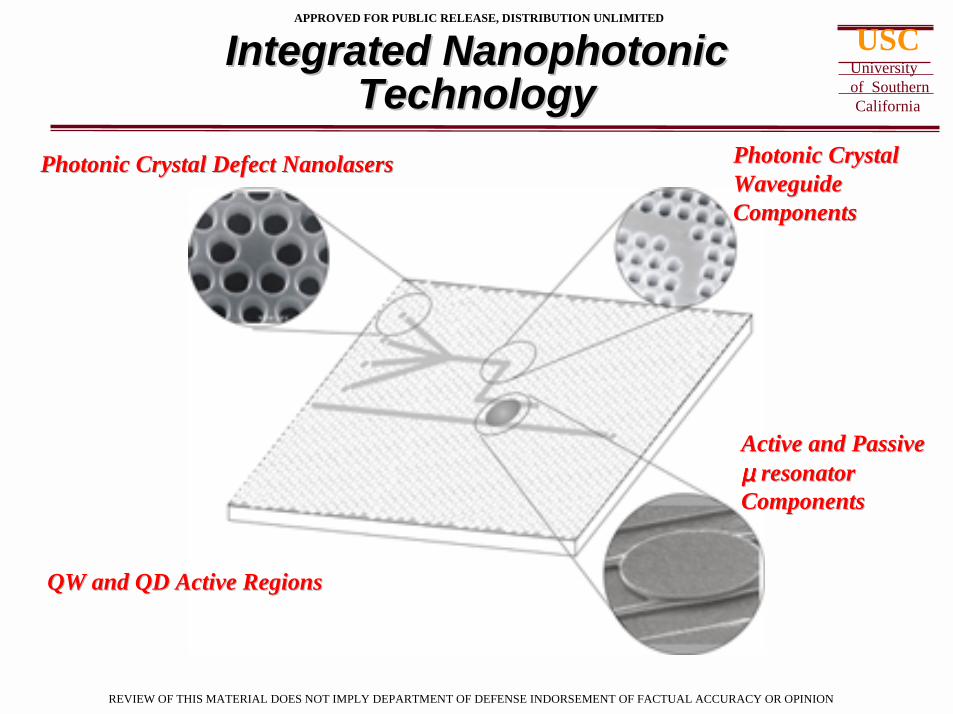
Integrated NanophotonicIntegrated NanophotonicTechnologyTechnology
Photonic Crystal Defect Photonic Crystal Defect NanolasersNanolasers Photonic Crystal Photonic Crystal Waveguide Waveguide ComponentsComponents
Active and PassiveActive and Passiveµµµµµµµµ resonator resonatorComponentsComponents
QW and QD Active RegionsQW and QD Active Regions
University of Southern California
USC
REVIEW OF THIS MATERIAL DOES NOT IMPLY DEPARTMENT OF DEFENSE INDORSEMENT OF FACTUAL ACCURACY OR OPINION
APPROVED FOR PUBLIC RELEASE, DISTRIBUTION UNLIMITED
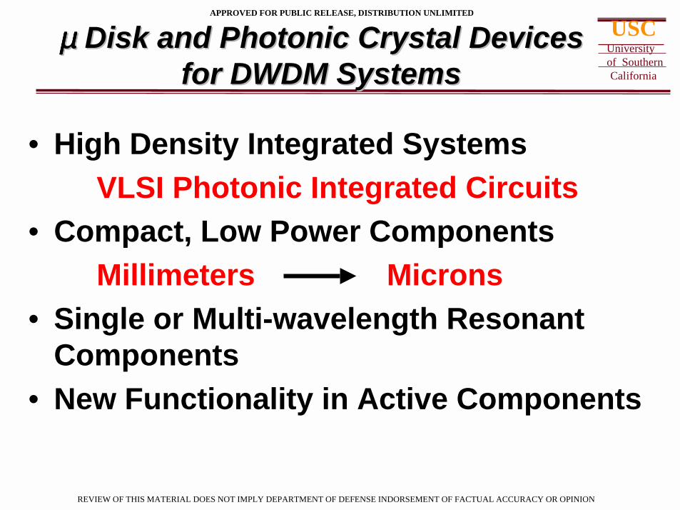
µµµµµµµµ Disk and Photonic Crystal Devices Disk and Photonic Crystal Devicesfor DWDM Systemsfor DWDM Systems
• High Density Integrated SystemsVLSI Photonic Integrated Circuits
• Compact, Low Power ComponentsMillimeters Microns
• Single or Multi-wavelength ResonantComponents
• New Functionality in Active Components

University of Southern California
USC
REVIEW OF THIS MATERIAL DOES NOT IMPLY DEPARTMENT OF DEFENSE INDORSEMENT OF FACTUAL ACCURACY OR OPINION
APPROVED FOR PUBLIC RELEASE, DISTRIBUTION UNLIMITED
Integrable Integrable NanophotonicNanophotonicComponentsComponents
!! DWDM DWDM µµµµµµµµ-Disk and -Disk and Nanolasers Nanolasers and Arraysand Arrays!! Tunable LasersTunable Lasers!! DispersiveDispersive, , SuperprismSuperprism Propagation Propagation!! Low Voltage, High Bit Rate ModulatorsLow Voltage, High Bit Rate Modulators!! Wavelength Selective SwitchesWavelength Selective Switches!! Narrow Band Tunable Filters and DetectorsNarrow Band Tunable Filters and Detectors!! Wavelength Selective Couplers and SplittersWavelength Selective Couplers and Splitters!! Chemical and Biological Sensor ElementsChemical and Biological Sensor Elements!! Waveguide to Fiber CouplersWaveguide to Fiber Couplers

University of Southern California
USC
REVIEW OF THIS MATERIAL DOES NOT IMPLY DEPARTMENT OF DEFENSE INDORSEMENT OF FACTUAL ACCURACY OR OPINION
APPROVED FOR PUBLIC RELEASE, DISTRIBUTION UNLIMITED
Nanophotonic Technologies
•• High Q ResonatorsHigh Q Resonators""Heterogeneous IntegrationHeterogeneous Integration""Electron Beam LithographyElectron Beam Lithography""Highly Asymmetric Dry EtchingHighly Asymmetric Dry Etching""Selective Area EpitaxySelective Area Epitaxy""QW and QD Active RegionsQW and QD Active Regions

University of Southern California
USC
REVIEW OF THIS MATERIAL DOES NOT IMPLY DEPARTMENT OF DEFENSE INDORSEMENT OF FACTUAL ACCURACY OR OPINION
APPROVED FOR PUBLIC RELEASE, DISTRIBUTION UNLIMITED
Selectively Grown Active RegionsSelectively Grown Active Regions
0 10 20 30 40 501.54
1.56
1.58
1.60
1.62
1.64
1.66
1.68
Lasi
ng W
avel
engt
h [ µ µµµ
m]
SAG stripe width [µµµµm], W
- 1000 µµµµm - 800 µµµµm - 750 µµµµm - 500 µµµµm - 400 µµµµm
I2,λλλλ2
I1,λλλλ1
Si3N4
W W
University of Southern California
USC
REVIEW OF THIS MATERIAL DOES NOT IMPLY DEPARTMENT OF DEFENSE INDORSEMENT OF FACTUAL ACCURACY OR OPINION
APPROVED FOR PUBLIC RELEASE, DISTRIBUTION UNLIMITED
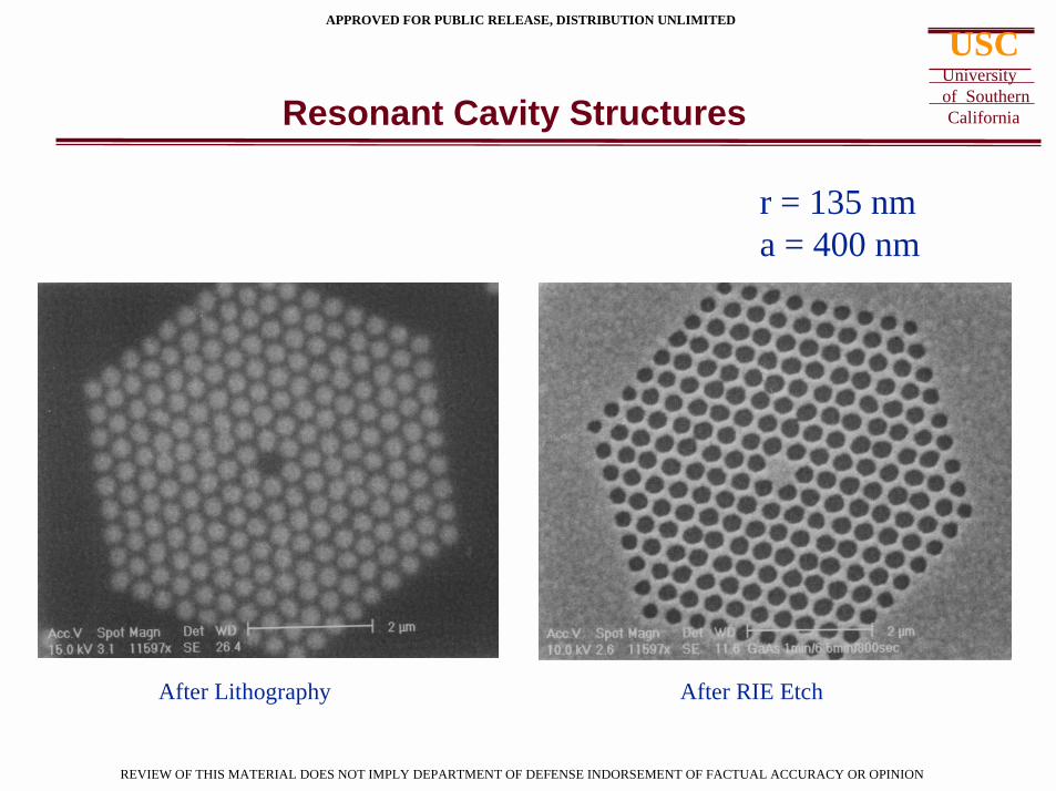
After Lithography After RIE Etch
r = 135 nma = 400 nm
Resonant Cavity Structures

University of Southern California
USC
REVIEW OF THIS MATERIAL DOES NOT IMPLY DEPARTMENT OF DEFENSE INDORSEMENT OF FACTUAL ACCURACY OR OPINION
APPROVED FOR PUBLIC RELEASE, DISTRIBUTION UNLIMITED
Top Views of GaAs PBGs after ECR etch

University of Southern California
USC
REVIEW OF THIS MATERIAL DOES NOT IMPLY DEPARTMENT OF DEFENSE INDORSEMENT OF FACTUAL ACCURACY OR OPINION
APPROVED FOR PUBLIC RELEASE, DISTRIBUTION UNLIMITED
Magnitude of the Electric Field in the Defect Cavity
top view
cross section
University of Southern California
USC
REVIEW OF THIS MATERIAL DOES NOT IMPLY DEPARTMENT OF DEFENSE INDORSEMENT OF FACTUAL ACCURACY OR OPINION
APPROVED FOR PUBLIC RELEASE, DISTRIBUTION UNLIMITED
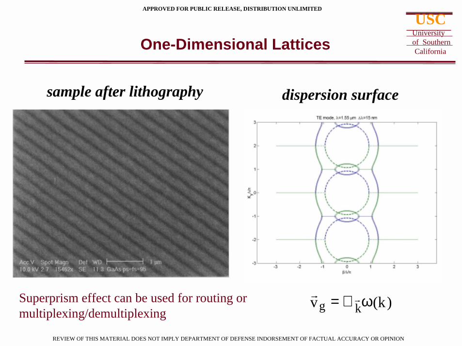
One-Dimensional Lattices
"!v g = ∇ "!
k ω(k)
sample after lithography dispersion surface
Superprism effect can be used for routing or multiplexing/demultiplexing

University of Southern California
USC
REVIEW OF THIS MATERIAL DOES NOT IMPLY DEPARTMENT OF DEFENSE INDORSEMENT OF FACTUAL ACCURACY OR OPINION
APPROVED FOR PUBLIC RELEASE, DISTRIBUTION UNLIMITED
Magnitude of the Electric Field in the Defect Cavity
top
bottom
top
bottom
symmetric cladding asymmetric cladding

University of Southern California
USC
REVIEW OF THIS MATERIAL DOES NOT IMPLY DEPARTMENT OF DEFENSE INDORSEMENT OF FACTUAL ACCURACY OR OPINION
APPROVED FOR PUBLIC RELEASE, DISTRIBUTION UNLIMITED
µ Resonator Structuresµ Resonator Structures
λλλλres2
λλλλres .
λλλλ1111,λ,λ,λ,λ2222, ...,, ...,, ...,, ...,λλλλres,................λλλλΝΝΝΝ
λλλλ1111,λ,λ,λ,λ2222, ....., ....., ....., .....λλλλΝΝΝΝ
λλλλ1111,λ,λ,λ,λ2222, ...,, ...,, ...,, ...,λλλλres,................λλλλΝΝΝΝ
λλλλres
λλλλ1111,λ,λ,λ,λ2222, ....., ....., ....., .....λλλλΝΝΝΝ
λλλλres1, λλλλres2
λλλλres1
Resonant Filter / Switch Resonant Y or Splitter
Resonant T or Splitter

University of Southern California
USC
REVIEW OF THIS MATERIAL DOES NOT IMPLY DEPARTMENT OF DEFENSE INDORSEMENT OF FACTUAL ACCURACY OR OPINION
APPROVED FOR PUBLIC RELEASE, DISTRIBUTION UNLIMITED
Vertical Coupler Fabricated byVertical Coupler Fabricated byHeterogeneous IntegrationHeterogeneous Integration
λλλλi
λλλλ1...λλλλN
λλλλ1.λλλλi-1..λλλλN
Laterally Coupled Disk • Air Couping • Sub Micron Control
��������������������������������������������
��������������������������������������������
������������������������������
������������������������������
OLD NEW
Vertically Coupled Disk • Epi Layer Coupling • Control Coupling by Epilayer Thickness
Transfer Substrate
Resonant Disk
Waveguides
• Add-Drop Filters• Resonant Detectors• Integrated Lasers• Resonant Modulators
University of Southern California
USC
REVIEW OF THIS MATERIAL DOES NOT IMPLY DEPARTMENT OF DEFENSE INDORSEMENT OF FACTUAL ACCURACY OR OPINION
APPROVED FOR PUBLIC RELEASE, DISTRIBUTION UNLIMITED
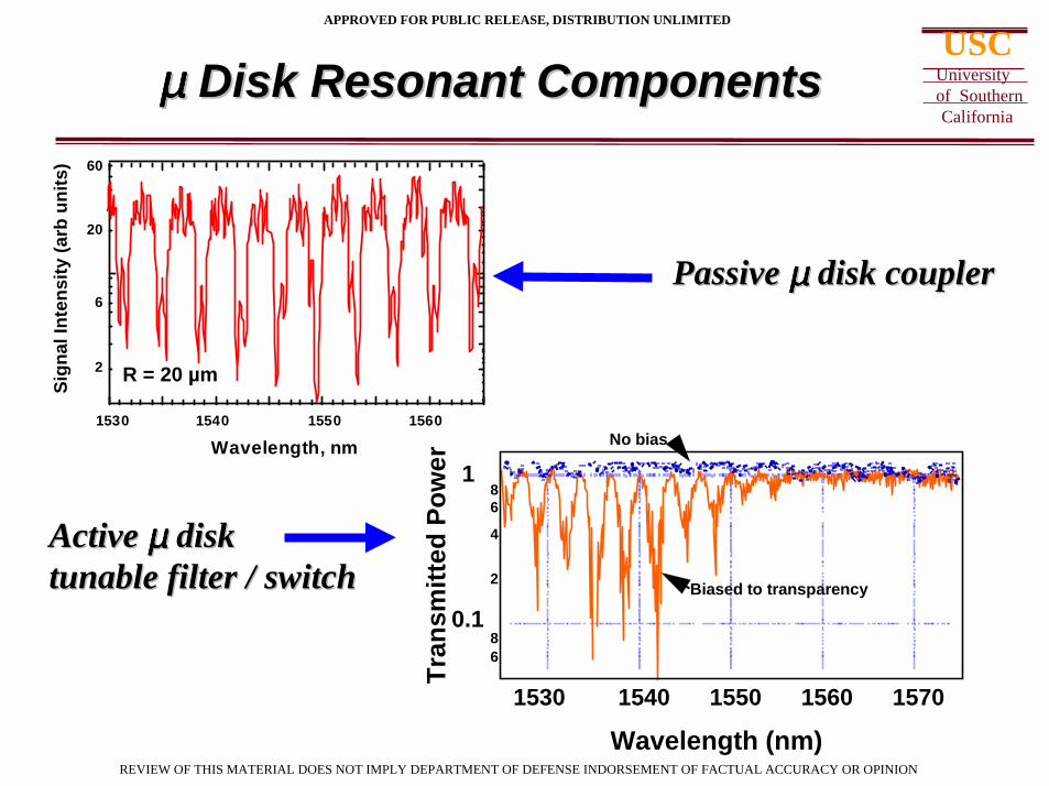
µµµµµµµµ Disk Resonant Components Disk Resonant Components
1560155015401530
Wavelength, nm
2
6
20
60
Sign
al In
tens
ity (a
rb u
nits
)
R = 20 µm
Passive Passive µµµµµµµµ disk coupler disk coupler
Active Active µµµµµµµµ disk disk tunable filter / switchtunable filter / switch
Tran
smitt
ed P
ower
6 8
0.1
2
4
6 8
1No bias
Biased to transparency
Wavelength (nm)1530 1540 1550 1560 1570