Embed Size (px)
Citation preview

This article was downloaded by: [Ohio State University Libraries]On: 16 March 2013, At: 18:30Publisher: Taylor & FrancisInforma Ltd Registered in England and Wales Registered Number: 1072954 Registered office:Mortimer House, 37-41 Mortimer Street, London W1T 3JH, UK
Contemporary PhysicsPublication details, including instructions for authors and subscriptioninformation:http://www.tandfonline.com/loi/tcph20
Nanomagnets for sensors and data storageK. J. KirkVersion of record first published: 08 Nov 2010.
To cite this article: K. J. Kirk (2000): Nanomagnets for sensors and data storage, Contemporary Physics, 41:2,61-78
To link to this article: http://dx.doi.org/10.1080/001075100181187
PLEASE SCROLL DOWN FOR ARTICLE
Full terms and conditions of use: http://www.tandfonline.com/page/terms-and-conditions
This article may be used for research, teaching, and private study purposes. Any substantialor systematic reproduction, redistribution, reselling, loan, sub-licensing, systematic supply, ordistribution in any form to anyone is expressly forbidden.
The publisher does not give any warranty express or implied or make any representation that thecontents will be complete or accurate or up to date. The accuracy of any instructions, formulae, anddrug doses should be independently verified with primary sources. The publisher shall not be liablefor any loss, actions, claims, proceedings, demand, or costs or damages whatsoever or howsoevercaused arising directly or indirectly in connection with or arising out of the use of this material.

Nanomagnets for sensors and data storage
K. J. K IRK
Miniaturized magnetic devices are ubiquitous in the hard disks of computers and in tape
storage systems. Giant magnetoresistance was discovered as recently as 1988 but already
sensors using the eŒect are being incorporated into read heads for the highest density hard
disk systems. As a result of intensive research and development, storage density on hard
disks has increased dramatically at a rate greater than 60% per year. At sub-micron and
nano-scale dimensions the properties of magnetic devices are strongly aŒected by their size
and shape in a complex way resulting from the interplay between diŒerent types of magnetic
energy. In some cases this causes a deterioration in the performance of existing devices,
however it has also enabled entirely new devices to be proposed. Arrays of nanomagnets
could be used for ultra-high density storage on hard disks or for fast and dense, non-volatile,
solid state memory. Storage applications are possible because hysteresis in the nanomagnets
creates two oppositely magnetized states which are stable in zero applied ® eld and can store
binary data . Magnetic sensors based on giant magnetoresistance in layered magnetic
structures are among the most sensitive available for operation at room temperature and
above. This paper describes the physical properties of nanomagnets and their role in present
and future applications.
1. Introduction
The magnetic data storage industry produced 140 million
hard disk drives worth $27 000 million in 1998 [1]. Over the
last 10 years the density of information stored on hard
disks has increased dramatically, with growth rates now
exceeding 60% per year. The rapid pace of technological
development towards higher density data storage has led to
an immense expansion of interest in magnetic materials,
especially thin ® lms, and has produced many spin-oŒs in
research and technology for sensors, new types of memory,
and even a new ® eld of electronics based on the spin of the
electron rather than its charge [2,3]. At the same time there
has been a strong push towards miniaturization, in many
cases the new devices will have dimensions deep in the
nanometre regime, and will be made from magnetic ® lms
only a nanometre or so thick.
Research into magnetic materials has been particularly
fruitful and new discoveries have been incorporated into
commercial products at unprecedented speed. Tradition-
ally, technologically useful magnetic materials fell into
two classes [4]: so-called `hard’ magnetic materials which
retain their magnetic state well and can therefore be
used as permanent magnets or as the thin ® lm coatings
which store information on disks or tapes; and `soft’
magnetic materials which have a large change in their
magnetic state for a small change in the external ® eld
and therefore are suitable as the active elements of
sensors. As we shall see, this traditional distinction
between hard and soft materials becomes less clear for
magnets of small dimensions, where a nanomagnet made
from a soft material may have ideal properties for data
storage.
The key recent discovery in magnetic materials was
giant magnetoresistance or GMR [5], a phenomenon in
which a material undergoes a large change in resistance
of typically 5± 40% when an external ® eld is applied.
When there is a large GMR response to a small ® eld
very sensitive magnetic ® eld sensors can be produced [6].
GMR sensors are already making inroads into magnetic
data storage in the recording heads for hard disks. The
GMR eŒect is most eŒectively exploited in layered
Author’ s address: Department of Physics and Astronomy, Department of
Electronics and Electrical Engineering, University of Glasgow, Glasgow
G12 8QQ, Scotland, UK.
Contemporary Physics, 2000, volume 41, number 2, pages 61± 78
Contemporary Physics ISSN 0010-7514 print/ISSN 1366-5812 online Ó 2000 Taylor & Francis Ltdhttp://www.tandf.co.uk/journals/tf/00107514.html
Dow
nloa
ded
by [
Ohi
o St
ate
Uni
vers
ity L
ibra
ries
] at
18:
30 1
6 M
arch
201
3

structures containing ferromagnetic and non-magnetic
layers. For example, devices such as spin valves and
spin tunnel junctions have been developed in which two
magnetic layers are sandwiched with a spacer layer of
either a non-magnetic metal or an insulator. There are
exciting possibilities for GMR devices as small cheap and
rugged sensors for use in navigation or mechanical
systems, and for magnetic random access memory
(MRAM ), a type of fast and dense non-volatile memory
which could eventually rival silicon DRAM [7,8].
Developments have also taken place in magnetically
hard materials for hard disk coatings known as media.
Up to four other metals are now alloyed with Co to
produce a granular ® lm with optimum properties for
recording. Hard disk media in current production are
magnetized in the plane of the disk, but materials are
also being investigated which are magnetized perpendi-
cular to the plane and could lead to higher density
storage than for in-plane recording [9]. Perpendicularly
magnetized media are already being used for magneto-
optical recording. In magneto-optical technology the data
is again stored in a magnetic coating on the disk but this
time is written and read with the help of a laser [10,11].
The data storage density in magneto-optical systems is
lower than on hard disk drives, since bit sizes are limited
by the wavelength of the light, but they are nevertheless
important for high density rewritable storage on remo-
vable disks. Near-® eld optical methods [12,13] could lead
to higher density magneto-optical recording, with bit
sizes far below the wavelength of the laser light, however
they are still not expected to exceed the storage densities
forecast for hard disks.
2. Looking at the eŒects of miniaturization
The trend in electronic devices is always towards miniatur-
ization. It is only necessary to think of the increase in
storage capacity of hard disks in personal computers over
recent years to realize that Gbytes of data are being
squeezed into a space which not long ago would have held
only a few Mbytes. In this section I will discuss some of the
eŒects on hard disk systems of miniaturizing their magnetic
components to sub-micron dimensions, and describe how
these eŒects are under investigation by magnetic imaging,
magnetic measurements and computer simulation.
2.1. Miniaturization issues in magnetic data storage
The basic components of a hard disk system are the disk
itself and the recording head. The most obvious way to
increase the density of data storage is for each piece of data,
or `bit’ , to be stored in a smaller space on the disk. With
miniaturization of the bits it follows that the other
components of the system must be miniaturized too.
At the heart of an advanced recording head is the
magnetoresistive sensor element. This is a small piece of
thin ® lm magnetic material which is a sensitive detector of
magnetic ® eld. Figure 1 shows a schematic diagram of the
sensor reading a sequence of bits. The data is written by a
tiny electromagnet, also built into the recording head,
which magnetizes a small part of the disk to create each bit.
Data is encoded as transitions’ which are changes between
two bits magnetized in opposite directions. The presence of
a transition indicates a binary 1 and the absence of a
transition (i.e. two adjacent bits written in the same
direction ) a binary 0. When data is being read, the vertical
M
magnetoresistivesensor element
strayfields
written bitson surfaceof diskdirection of
travel of disk
bitlength
trackwidth
Figure 1. Magnetoresistive sensor element reading bits on a hard disk. The magnetization M of the sensor element changes its direction
due to the stray magnetic ® eld (pointing up or down) at the transitions between bits. An alternating pattern of bits, as shown here, would
be read as a sequence of binary 1s.
K. J. Kirk62
Dow
nloa
ded
by [
Ohi
o St
ate
Uni
vers
ity L
ibra
ries
] at
18:
30 1
6 M
arch
201
3
magnetic ® eld at the transition changes the orientation of
the magnetization in the sensor, causing an increase or
decrease in resistance.
The bits on a hard disk are arranged in concentric
circular tracks. Therefore, to increase the density of stored
information, the bit length (the distance between transi-
tions) and the track width both need to shrink. Recent
milestones for storage density in demonstration systems are
16 Gb inÐ 2
, from drive manufacturer Seagate Technology
in March 1999 [14] and 20.7 Gb inÐ 2
from the Read-Rite
Corporation in May 1999. For the 20.7 Gbit inÐ 2
record,
the bits were 55 nm wide, there were 1700 tracks per
millimetre, and the recording head was travelling only
15 nm from the disk. Seagate recently announced (June
1999 ) a dramatic increase in track density to over 4100
tracks per millimetre by improving the accuracy with which
their recording heads could follow narrower tracks.
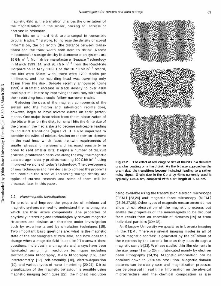
Reducing the sizes of the magnetic components of the
system into the micron and sub-micron regime does,
however, begin to have adverse eŒects on their perfor-
mance. One major issue arises from the miniaturization of
the bits written on the disk: for small bits the ® nite size of
the grains in the media starts to become noticeable, leading
to indistinct transitions ( ® gure 2). It is also important to
consider the eŒect of miniaturization on the sensor element
in the read head which faces the twin requirements of
smaller physical dimensions and increased sensitivity in
order to read smaller bits. Despite a number of di� cult
practical problems to be solved along the way, the magnetic
data storage industry predicts reaching 100 Gbit inÐ 2
using
improved versions of today’ s technology. The development
of new techniques and new devices to combat the problems
and continue the trend of increasing storage density are
topics of current research and some of them will be
discussed later in this paper.
2.2. Nanomagnetic investigations
To predict and improve the properties of miniaturized
magnetic systems we need to understand the nanomagnets
which are their active components. The properties of
physically interesting and technologically relevant magnetic
structures and devices are therefore under investigation
both by experiments and by simulation techniques [15].
Two important basic questions are: what is the magnetic
state of the nanomagnets at zero ® eld, and how does this
change when a magnetic ® eld is applied? To answer these
questions, individual nanomagnets and arrays have been
fabricated using high resolution techniques including
electron beam lithography, X-ray lithography [16], laser
interferometry [17], self-assembly [18], electro-deposition
[19], and various types of nano- imprinting [20,21]. Direct
visualization of the magnetic behaviour is possible using
magnetic imaging techniques [22], the highest resolution
being available using the transmission electron microscope
(TEM ) [23,24] and magnetic force microscopy (MFM )
[25,26,27,28]. Other types of magnetic measurement do not
allow direct observation of the magnetic processes but
enable the properties of the nanomagnets to be deduced
from results from an ensemble of elements [29] or from
individual particles [30 ± 33].
At Glasgow University we specialize in Lorentz imaging
in the TEM. There are several imaging modes in all of
which magnetic contrast is generated by the de¯ ection of
the electrons by the Lorentz force as they pass through a
magnetic sample [23]. We have studied thin ® lm elements in
the size range 4 l m to 25 nm, fabricated mainly by electron
beam lithography [34,35]. Magnetic information can be
obtained down to 2± 20 nm resolution. Magnetic domain
patterns can be clearly seen and magnetization processes
can be observed in real time. Information on the physical
microstructure and the chemical composition is also
Figure 2. The eŒect of reducing the size of the bits in a thin ® lm
granular coating on a hard disk. As the bit size approaches the
grain size, the transitions become indistinct leading to a rather
noisy signal. Grain size in the Co alloy ® lms currently used is
typically 12± 15 nm, compared with a bit length of < 55 nm.
Nanomagnets for sensors and data storage 63
Dow
nloa
ded
by [
Ohi
o St
ate
Uni
vers
ity L
ibra
ries
] at
18:
30 1
6 M
arch
201
3

available from the TEM and can be correlated with the
observed magnetic microstructure to give a complete
picture of how the magnetic properties are aŒected by
defects, grain size and irregularities.
Advances in computer modelling combined with im-
provements in high resolution lithography and imaging
over the last ten years mean that experimental and
simulated results can now be compared for nanomagnetic
systems. Theoretical work on nanomagnets has helped to
clarify some details of the magnetic processes, explore the
parameters required for improved devices, and extend our
understanding into regimes which are di� cult to access
experimentally, such as extremely fast time-scales and very
tiny elements.
3. Properties of small magnetic elements
In this paper I shall concentrate on the properties of thin
® lm elements of micro-polycrystalline soft magnetic mate-
rial such as Ni80Fe20 (NiFe) and pure Co. These sorts of
magnetic ® lms, patterned into elements with micron and
sub-micron dimensions, have proved to be versatile for a
wide range of applications in sensors, memory elements and
data storage. Their behaviour is strongly aŒected by their
shape and size in the micron and nano-scale regime, as we
shall see.
3.1. Magnetic domain structures
We will now begin to look at the magnetization distribution
within a thin ® lm element of magnetic material. M (r ) is the
magnetization vector at each point, where |M | = M s is the
saturation magnetization. M s is a characteristic of the
material and has a constant value in a sample of uniform
composition. It is the orientation of M which varies
throughout the sample giving rise to the huge variety of
domain patterns observed.
Figure 3 shows magnetic images of square and rectan-
gular elements of NiFe ® lm, 20 nm thick. The elements are
shown in plan view in the TEM. They are magnetized in the
plane of the ® lm with magnetization distributions shown in
the schematic diagram, ® gure 3 (d ). In ® gures 3 (a ) and (b )
(Foucault mode) the light and dark shading shows the
magnetic domains, which are areas of more or less constant
magnetization. In each case, white and black indicate
opposite magnetization directions parallel to the double-
headed arrow, while domains magnetized perpendicular to
the arrow appear grey. Using another imaging mode,
known as the Fresnel mode, ® gure 3 (c ) shows the domain
walls which form the boundaries between the domains. At a
domain wall the magnetization rotates, usually by 90 8 or
180 8 , from one domain to the next. These elements have
`¯ ux closure’ domain patterns in which the magnetization
in the elements forms a closed loop.
The diŒerent domain patterns result from the competing
magnetic in¯ uences in micron and sub-micron sized
elements. The exchange interaction, a consequence of the
quantum mechanical origin of magnetism, attempts to have
the whole of the element magnetized the same way. To
minimize the magnetostatic energy, however, the magneti-
zation would like to split into many domains, to form
closed magnetic loops and minimize the stray ® elds. The
magneto-crystalline anisotropy, meanwhile, would prefer
the magnetization to lie along certain crystal axes in the
material, or, in a polycrystalline material, along a preferred
direction (or easy axis) sometimes created by growing the
® lm in an applied ® eld. In addition, the element experiences
the magnetizing eŒect from any external magnetic ® eld.
In a nanomagnet of soft magnetic material at zero ® eld,
the dominant eŒects are from the competition between the
exchange energy and the magnetostatic energy. When the
magneto-crystalline anisotropy is very low, or when it
averages to zero in a polycrystalline material, the magne-
tization has no preferred directions and is quite happy to
follow the edges of the element, as was clearly seen in the
¯ ux closure domain patterns in ® gure 3. A diŒerent type of
domain structure is seen in more elongated rectangles in
® gure 4. These elements take up a `near single domain’ state
with uniform magnetization in most of the element, except
for small domains at the ends where the magnetization
(a)
(c)
Figure 3. Magnetic domains in NiFe elements observed by two
diŒerent Lorentz imaging modes in the transmission electron
microscope. In Foucault mode, (a ) and (b), we can see the
direction of magnetization in the domains (white and black
indicate opposite magnetization directions parallel to the double
headed arrows). In Fresnel mode, (c), the domain walls are
visible. These elements have a ¯ ux closure domain structure in
which the magnetization forms closed loops as shown in the
schematic diagram (d ). The dimensions of the elements are
2 l m ´ 2 l m, 1 l m ´ 2 l m, 2 l m ´ 1 l m and 1 l m ´ 1 l m. Film
thickness is 20 nm.
K. J. Kirk64
Dow
nloa
ded
by [
Ohi
o St
ate
Uni
vers
ity L
ibra
ries
] at
18:
30 1
6 M
arch
201
3

loops round to achieve partial ¯ ux closure, thereby
reducing, but not eliminating, the stray ® eld. For complete
¯ ux closure in these elements it would be necessary to have
either a very long central domain wall running parallel to
the long axis or a high density of shorter walls running
transversely. Neither of these scenarios would be favoured
by the exchange interaction since they would entail
deviation from uniform magnetization over a large part
of the element.
We have seen that domain walls exist at the boundaries
between domains of diŒerent magnetization direction.
Inside the wall the magnetization must somehow swing
round from one direction to another. In fact there are a
number of wall types with characteristic width and
properties [36]. In soft thin ® lms Ne el walls predominate
in which the magnetization vector stays parallel to the
plane of the ® lm while it gradually rotates from one
direction to the next. In a magnetic ® lm with low
anisotropy, such as NiFe, this will cost very little
magnetostatic or magneto-crystalline energy. To minimize
the energy, the exchange interaction tries to enforce a very
slow change in the magnetization direction across the wall.
Therefore Ne el walls are very wide, about 200 nm in a
continuous ® lm. For many years it was tempting to believe
that walls could not form inside nanomagnets narrower
than a standard wall width Ð therefore they would be truly
single domain. However it has been clearly shown by high
resolution magnetic imaging that domain walls can indeed
be accommodated. The walls themselves will no longer be
simple Ne el walls but will have a more complicated
structure, with their detailed form depending on the
thickness of the ® lm [37].
The concept of shape anisotropy is particularly impor-
tant in small elements. This is the tendency for the
magnetization to align along the length of the element,
creating an easy axis de® ned by the shape. Shape
anisotropy minimizes the magnetostatic energy by keeping
the magnetization parallel to the long edges of an element.
More stray ® eld, and therefore more stray ® eld energy, is
generated if the magnetization meets head-on the long
edges of a rectangle rather than the shorter ones. For the
same reason, the magnetization in a continuous thin ® lm
usually lies in the plane of the ® lm rather than perpendi-
cular to it.
3.2. Switching ® elds and switching mechanisms
It is quite clear, then, that the shape of a nanomagnet has a
very strong eŒect on its domain patterns. These in turn
aŒect its magnetic properties, such as its switching ® eldÐ
the ® eld required to switch the magnetization from one
direction to the opposite direction. For example, elongated
rectangular elements (as seen in ® gure 4 ) have been found
to have certain characteristic properties. The magnetization
aligns along the long axis and a single domain occupies
most of the element: therefore there are two stable magnetic
states. The coercivity of an element can easily be more than
100 times the coercivity of an unpatterned soft magnetic
® lm of the same material. The element width has a strong
eŒect on the applied ® eld needed to switch between the two
stable states. Figure 5 shows how the switching ® eld of Co
and NiFe elements of a similar thickness, applied parallel to
the long axis of the elements, increases as the width
decreases.
It is also important to know the mechanism by which
switching occurs. In general, switching will proceed by
some combination of three basic mechanisms: rotation of
the magnetization within a domain, growth of existing
domains, or formation of new domains. For example,
observations in the TEM on elongated rectangular nano-
magnets made from NiFe and Co have shown that
switching starts by growth of the ¯ ux closure domains at
the ends [38]. Above an aspect ratio (length/width ) of about
4 : 1 there is no eŒect from the element’ s length on its
switching ® eld. This tells us something else about the
switching mechanism in these elongated elementsÐ switch-
ing occurs independently from one end or the other with no
interaction between the end domains.
Information on the switching ® elds and mechanisms
gives a good indication of how the geometry of a
nanomagnet could be modi® ed in order to alter its
magnetic properties. In the case of elongated elements
the switching ® eld is more than doubled if the end
(a) (b)1µmµ
Figure 4. Domain structure in elongated rectangles
4 l m ´ 1 l m and 4 l m ´ 0.5 l m, made from a NiFe ® lm
26 nm thick: (a) magnetic image and (b ) schematic. Complete
¯ ux closure is not possible in these elements so they become
predominantly magnetized along their length. Vortex-type
domains commonly form at the ends. Stray ® elds can be seen
outside the elements as dark shading at the ends and lighter
shading at the sides.
Nanomagnets for sensors and data storage 65
Dow
nloa
ded
by [
Ohi
o St
ate
Uni
vers
ity L
ibra
ries
] at
18:
30 1
6 M
arch
201
3

domains are suppressed by changing the ends of the
element from a rectangular to a pointed shape [39].
Because they have two stable magnetization states,
elongated elements are suitable for data storage applica-
tions. The two opposite states can be used to store
binary data and the high switching ® eld gives the
elements stability to retain the data against external
magnetic in¯ uences.
3.3. Predicting the behaviour of nanomagnets
3.3.1. Stable states. For a long time attempts have been
made to predict the behaviour of small magnetic elements,
to enhance our knowledge of the physics of magnetism at
small dimensions and as a tool for the development of new
magnetic devices and systems. Therefore micromagnetic
models have been produced which consider the in¯ uences
acting on the system and show the probable resulting
domain patterns.
An eŒective method to predict stable magnetization
con® gurations, the ones seen in real systems, is to calculate
the energy minima of the system using the magnetic Gibbs
free energy. The magnetic Gibbs free energy is the sum of
the relevant magnetic energy terms, generally including the
exchange energy, the magnetostatic energy, the magneto-
crystalline anisotropy energy and the potential energy of
the system in the external applied ® eld. Stable states are
therefore local minima on a complex energy surface.
During a magnetization cycle, the system follows a route
over this energy surface, which will be distorted by changes
in the applied ® eld. Magnetic hysteresis arises because in
general the same route cannot be retraced on the reverse
path.
Equations for the most important terms of the magnetic
Gibbs free energy are given below. In each case the energy
is integrated over the volume, V, of the system. The total
free energy, E tot, is the sum of these terms. At a stable state,
E tot has a local minimum, subject to the constraint that |M |
remains constant throughout the system.
Exchange energy
Eex 5
Z
V
AX3
i 5 1
Ñ b i( )2
dV , (1)
Magnetostatic energy
Emag 5 2 12
Z
V
Hd . ¹0M( ) dV , (2)
Magneto-crystalline anisotropy energy
Ean 5 2Z
V
Ku u . b( )2
dV , (3)
Magnetic potential energy
Epot 5 2Z
V
Happ . ¹0M¡
dV . (4)
Here M is the magnetization vector and b is the direction
cosine of the magnetization vector (M = M s b ). A is the
exchange constant [40] and l 0 is the permeability of free
space. H app is the external applied ® eld, Hd is the self-
demagnetizing ® eld, Ku is the uniaxial anisotropy constant
of the material and u is the anisotropy direction.
Looking at the equations, we can get an idea of what
factors determine the magnitude of these terms. Exchange
energy (1) depends on the rate of change in angle of the
magnetization vector from one point to the next. If the
angle of M is steeply varying, as it could be in a domain
wall, the exchange energy will be large. The factor A, the
exchange constant, is analogous to an elastic constant for
the magnetic material. The magnetostatic energy contribu-
tion (2) to the total depends strongly on the sample
geometry, via the demagnetizing ® eld. This can be di� cult
to determine precisely since the magnetization con® gura-
tion inside the sample is aŒected by the stray ® elds it
produces itself. Some simple cases and useful approxima-
tions are described below. The magneto-crystalline energy
(3) lowers the total energy if M lies along u, the easy axis of
the material. In NiFe K u is small so this energy contribu-
tion may be negligible compared to the other terms,
especially for nanomagnets. The magnetic potential energy
(4) is generated by applying an external ® eld. This term will
most eŒectively minimize the total energy if the magnetiza-
tion in the sample aligns in the same direction as the
applied ® eld.
Co 25nm thick
NiFe 26nm thick
30 50 70 90 110
element width (nm)
0
500
1000
1500
switc
hing
fie
ld (
Oe)
Figure 5. Increase of switching ® eld of rectangular nano-
magnets of NiFe and Co as their width is decreased. The aspect
ratio of these elements (length/width) was between 3.75 and 10
but in this range it had little eŒect on the switching ® eld.
K. J. Kirk66
Dow
nloa
ded
by [
Ohi
o St
ate
Uni
vers
ity L
ibra
ries
] at
18:
30 1
6 M
arch
201
3

The demagnetizing ® eld H d depends on the geometry of
the system via a demagnetizing factor, N , de ® ned by
H d 5 2 NM . (5 )
A simpli® cation frequently made for a thin ® lm element is
to approximate it by a uniformly magnetized, very oblate,
ellipsoid with its two major axes the same as the length and
width of the element [41]. The two in-plane dimensions a
and b must be much larger than the thickness c. The
demagnetizing factor when the sample is magnetized along
the long axis, a, in the plane of the ® lm is then
Na 5p4
c
a1 2
1
4
a 2 b
a2
3
16
a 2 b
a
2
(6)
and for the sample magnetized along the short axis, b, also
in the plane, is
Nb 5p4
c
a1 1
5
4
a 2 b
a2
21
16
a 2 b
a
2
. (7)
The out-of-plane demagnetizing factor N c is related to Na
and Nb by
Na 1 Nb 1 Nc 5 1 . (8)
Nc should be ~ 1 if the assumption of a very oblate ellipsoid
is correct. For an element measuring 1 l m ´ 200 nm ´ 25
nm, the demagnetizing factors in the plane of the ® lm are
Na = 0.013 along the length and Nb = 0.023 across the
width. For out-of-plane magnetization, Nc = 0.96. With no
external ® eld and negligible magneto-crystalline anisotro-
py, the magnetization will orientate in the direction giving
the smallest demagnetizing ® eld in (5 ), i.e. along the long
axis a. This is the origin of shape anisotropy. Clearly if the
in-plane dimensions of a nanomagnet are very small they
could become comparable to the ® lm thickness and the
assumption of a very oblate ellipsoid (a > b > > c ) will no
longer be valid. If a diŒerent approximation cannot be
used, numerical methods are then needed to calculate the
demagnetizing ® eld.
A very useful simpli® cation of the total energy of a
magnetic element is given by the Stoner± Wohlfarth
equation, which can be used to predict switching ® elds
and hysteresis loops of a uniformly magnetized magnetic
sample. The total Stoner± Wohlfarth energy of the element
is
ES W 5 K s in2
u 2 H e a s y M s c o s u 2 H h a r d M s s in u , (9 )
where K is the uniaxial anisotropy constant, } is the angle
between M in the element and the easy axis, and H ea sy and
Hhard are the applied ® eld components, parallel and
perpendicular to the easy axis, in the plane of the element.
For the Stoner± Wohlfarth equation to be applicable the
magnetization in the element must be uniform throughout
and must be assumed to rotate coherently under the
in¯ uence of the applied ® eld. There must be a single easy
axis (uniaxial anisotropy). The anisotropy constant K can
either refer to the magneto-crystalline anisotropy, with
constant Ku, or the shape anisotropy using the stray ® eld
energy constant Kd,
Kd 5¹0M 2
s
2, (10 )
whichever dominates in the element in question.
Using (9 ) the total energy for each orientation of M can
be found for diŒerent values of applied ® eld. Therefore the
stable directions of magnetization in the element can be
identi ® ed as the orientations of M giving energy minima.
When changing the external ® eld an energy minimum may
disappear, so if the system was previously stable in that
minimum it must go to a new, lower, minimum. If the
applied magnetic ® eld is opposite to the initial magnetiza-
tion direction, complete switching may occur. The Stoner±
Wohlfarth assumption that the system switches by coherent
rotation of M is necessary so that uniform magnetization is
preserved at all times. However we know that in real
systems it is common for the magnetization in an element
to change by means of domain processes, so the Stoner±
Wohlfarth value for the switching ® eld will be an over-
estimate [42]. Nevertheless it is useful as an upper bound to
the switching ® eld, and to predict some general trends.
3.3.2. Dynamic solutions. Even when using energy mod-
els more complex than the Stoner± Wohlfarth picture, there
is ample experimental evidence that modelling magnetiza-
tion reversal by considering only the stable states at the
energy minima is not completely reliable. For example,
some energy states may have very similar energy, such as in
the 2 l m ´ 1 l m and 1 l m ´ 2 l m elements in ® gure 3,
which makes the end result very sensitive to the exact path
by which reversal takes place [43]. Therefore dynamic
solutions can be used to determine the magnetic state of an
element during a particular ® eld cycle. In this picture, the
system stays in an energy minimum until the minimum
disappears, as in the static methods, but then follows the
dynamic equations to reach a new stable state.
Another limitation of static energy minimization meth-
ods for micromagnetic modelling is that they do not take
into account the speed of reversal. With increasingly fast
systems being used for data storage it becomes necessary to
investigate high frequency processes where a quasi-static
approach is inadequate and dynamic modelling is vital.
Most dynamic models work by taking H eΠas the
eŒective ® eld acting on a particular point in the magnetic
sample. Equilibrium is reached when
Heff 5 2 E tot
M, (11 )
so the system is at a local minimum in energy, and
M 3 H eff 5 0, (12 )
Nanomagnets for sensors and data storage 67
Dow
nloa
ded
by [
Ohi
o St
ate
Uni
vers
ity L
ibra
ries
] at
18:
30 1
6 M
arch
201
3

so the torque on the magnetization is zero. When a new
external ® eld is applied, the magnetization precesses around
the ® eld direction according to
1
c
M
t5 M 3 H eff, (13 )
where c is the gyromagnetic ratio for an electron. Energy
dissipation is brought into the equations via a damping
term, a , which is found from ferromagnetic resonance
experiments and is usually in the range 0.01 ± 1. a represents
critical damping. When damping is included E tot decreases
over time and M rotates towards H eΠuntil parallel so the
torque is again zero. For full equations incorporating the
damping term, see [43].
Both dynamic micromagnetic simulations and those
based on energy minimization require numerical techniques
on high speed computers to calculate the demagnetizing
® eld of the system and perform the minimization or
integrate the equation of motion for M . The ® rst step in
this kind of modelling is to discretize the magnetic element
into smaller volumes with edge size of the order of the
exchange length, ex ,
ex 5A
M 2s
1 /2
. (14 )
Within each discretization volume, the magnetization can,
justi® ably, be assumed to be uniform so an equation can be
written for its energy, E tot, in the applied ® eld. As ex is just
a few nanometres it becomes clear why nano-scale magnetic
elements are easier and quicker to model than larger ones
where discretization produces many thousands of equations
to be solved.
4. Applications of nanomagnetics in new technology
Nanomagnetic systems are an important part of today’ s
technology and have potential for new devices for the
future. In this section I will discuss three main
applications of nanomagnets: proposed patterned media
for hard disks; miniature magnetic sensors employing
the GMR eŒect, currently used in advanced recording
heads; and magnetic memory cells or MRAM which
are being developed for fast and dense solid state
memory.
4.1. Patterned media for hard disks
The trend towards hard disks with a greater storage density
still seems unstoppable and the increase in storage density
is actually accelerating rather than slowing down. However
eŒects associated with the ® nite grain size of magnetic
alloys used for storage could prevent inde® nite miniatur-
ization [44]. To reach ultra-high storage densities, a new
type of storage media has been proposed made from a
closely-packed array of nanomagnets patterned onto a hard
disk [45].
4.1.1. The superparamagnetic limit. Conventional hard
disk media are continuous ® lms of granular Co alloys.
Writing data on the disk involves aligning the magnetiza-
tion of a small area of the media. The ® lms used for media
are specially designed so that the grains are `exchange-
decoupled’ . This means that each grain reverses individu-
ally and very localized areas of the disk can be written,
enabling the bits to be very small and well de® ned.
Intergranular exchange coupling is suppressed by adding
non-magnetic ingredients, in particular Cr, which segregate
to the grain boundaries breaking the ferromagnetic
connection between the grains. At the same time the
signal-to-noise ratio and the coercivity of the medium must
be optimized. Magnetostatic interactions between the
grains will still occur and each grain needs to have a high
coercivity in order to withstand the magnetostatic in¯ uence
of its neighbours.
In the quest for smaller bits, the size of the grains has been
steadily reduced. Smaller grains help avoid uneven transi-
tions between bits and ensure a minimum number of grains
per bit to limit statistical noise. However there is a danger in
continuing to reduce the grain size of the media. If the grains
are too small, their magnetic energy becomes comparable to
their thermal energy and their magnetization direction can
switch freely, like the atoms in a paramagnetic material. Of
course, if individual grains on a hard disk are susceptible to
thermal switching at room temperature then the stored
information will rapidly disappear. The limit on grain size is
known as the superparamagnetic limit and has been
predicted to be around 10 nm using current media [46].
Smaller grains can only be used if their switching ® eld is
increased. This is in fact possible by altering the composi-
tion of the Co alloy. Higher coercivity, around 3500 Oe, has
been achieved by moving to four and ® ve component Co
alloys incorporating Ta and Pt to increase the magneto-
crystalline anisotropy of the grains [47,48]. Even greater
coercivity, up to 10 000 Oe, would be possible if hard
magnet materials such as SmCo or NdFeB were used as
media. With this coercivity, grain sizes could in theory be
reduced to 2.5 nm. However this would put impossible
demands on the write heads available today, which are
limited to write ® elds of 5000 Oe. This is a key problem
facing the hard disk industry in its plans for the future. One
solution could be thermally assisted writing, where the
coercivity of the media would be weakened locally using a
laser pulse to make it easier to magnetize.
4.1.2. Requirements for patterned media. Higher storage
densities, in the 100 ± 500 Gbit inÐ 2
range, could be
reached using patterned media. Instead of a bit being a
collection of exchange-decoupled grains, it would be an
K. J. Kirk68
Dow
nloa
ded
by [
Ohi
o St
ate
Uni
vers
ity L
ibra
ries
] at
18:
30 1
6 M
arch
201
3

individual nanomagnet made from an exchange-coupled
® lm like NiFe. The media would then consist of an array of
nanomagnet bits, physically isolated from their neighbours
and able to be switched independently. The strong
intergranular exchange coupling within the ® lm ensures
that all the grains in a bit switch at once. Depending on the
material, a nanomagnet bit could be thermally stable down
to around 10± 20 nm in size, leading to ultra-high storage
densities. At the same time the switching ® elds would be of
moderate size, thus reducing the demands on the write
head. Sharp transitions between bits are guaranteed by
lithographic patterning. The signal-to-noise requirement to
have many grains per bit no longer appliesÐ therefore
extremely small grain sizes are not required.
To store one bit of data, each nanomagnet must have
two distinct magnetization states. This is easily achieved
using elongated elements of soft magnetic materials with
uniaxial shape anisotropy. The bits could be oriented either
in the plane of the disk or perpendicular to it. Suitable
candidates (shown in ® gure 6 ) are (a ) bars patterned in the
plane of the disk, (b) pillars with their long axis vertical
[49], or (c) cones. A perpendicular con® guration allows the
nanomagnets to be packed more densely, whilst an in-plane
con® guration would enable more conventional reading and
writing technology to be used.
Figure 7 shows an image from the transmission electron
microscope showing nanomagnet bars of Co ® lm, with
nominal dimensions 200 nm ´ 40 nm and thickness 25 nm,
fabricated at Glasgow. With one bit stored per element, this
would correspond to a storage density of 27 Gb inÐ 2
.
Magnetic imaging shows the Co nanomagnets to be
magnetized along their length. Their average switching
® eld is 1200 Oe. The sequence of magnetic images in ® gure 8
show how an array of NiFe nanomagnets of the same size
reverse their magnetization in an applied ® eld. These have a
lower average switching ® eld of around 800 Oe. Research-
ers elsewhere have shown that it is possible to write `data ’
to nanomagnet arrays by reversing the magnetization of
individual elements, usually using the localized ® eld from
the probe of a magnetic force microscope [50]. It has also
been possible to detect the magnetization direction of
perpendicular Ni pillars using an ordinary read head
scanned across an array [51].
The packing density of an array is limited by magneto-
static interactions between adjacent elements. Interactions
have the eŒect of lowering or raising the switching ® eld
compared to what would be expected for an isolated
element. Depending on the magnetization state and
position of the neighbours, demagnetizing or magnetizing
eŒects will occur. For example we have seen that the
distribution of switching ® elds was widened in an array of
elements arranged side by side when their spacing was
made the same as their width or smaller [39]. It is important
that the eŒect of interactions does not cause an element to
switch at too low a ® eld so it could be accidentally
overwritten during writing of its neighbours, or at too high
(a)
(b)
(c)
Figure 6. Possibilities for patterned media: (a) bars in the plane
of the disk, (b ) perpendicular pillars and (c) cones. Nanomagnets
for data storage on hard disks must have two distinct
magnetization states. This can be achieved using the special
shape-controlled properties of elongated elements.
50nm
Figure 7. Co nanomagnet bars 200 nm ´ 40 nm, 25 nm thick,
fabricated by electron-beam lithography and viewed in the
transmission electron microscope. With one bit stored per
element this would correspond to a storage density of
27 Gbit inÐ 2
.
Nanomagnets for sensors and data storage 69
Dow
nloa
ded
by [
Ohi
o St
ate
Uni
vers
ity L
ibra
ries
] at
18:
30 1
6 M
arch
201
3

a ® eld so it would fail to be written by the recording head.
To avoid these problems, the size, shape, and aspect ratio
of the elements in the nanomagnet array must be tailored
for optimum density and performance.
4.1.3. Practical issues for mass production. If patterned
media are to be taken up for commercial hard disk systems,
cost eŒective methods of mass production of magnetic
nano-elements must be developed. Most of the fabrication
methods used in research on nanomagnets would not be
suitable. Electron beam lithography is highly versatile and
can produce very small elements, but is a rather slow serial
process. Laser interference lithography can be used to cover
large areas at once but is restricted to regular rectangular
arrays [52]. More promising pattern transfer techniques are
nano-imprint lithography [53] or embossing [54] which use
electron beam fabricated master moulds, or some kinds of
`soft lithography’ in which ¯ exible moulds are used [55].
Ion beam modi® cation of a continuous ® lm would have the
bene® t of retaining a smooth and ¯ at recording surface [56].
In recent experiments using ion beam bombardment,
magnetically softer areas with in-plane magnetization were
created in perpendicularly magnetized CoPt multilayers by
mixing the layers.
New recording head designs will also be needed for
patterned media, particularly if the stray ® eld from the
nanomagnet bars or pillars is in a diŒerent direction from
that in current systems. It will also be necessary to
synchronize writing the data with the position of the bits.
This will involve greater control of the head position and
more servo information, describing the exact position of the
elements, to be written on the disk. If the bits are too small
to read and write using conventional recording heads,
alternative techniques will be needed to access the data [57].
4.2. GMR sensors
Sensors based on GMR are an exciting class of device with
applications in mechanical and navigational systems, as
well as their major use in read heads for hard disks. The
origin of the GMR eŒect is the diŒerence in scattering of
electrons of opposite spin (up or down) as they pass
through a ferromagnetic material [3,58]. For a particular
orientation of magnetization in the material this spin-
dependent scattering will lead to one type of electron
experiencing a higher resistivity than the other.
4.2.1. The GMR eŒect. Layered magnetic structures
have proved most useful for GMR devices. Spin-dependent
scattering occurs in the magnetic layers and at the
interfaces. For example, a simple GMR sensor could
consist of two magnetic layers which can have their
magnetization oriented either parallel or antiparallel to
each other. When the two layers are magnetized antipar-
allel, the spin-up and spin-down electrons will be scattered
equally. However, when the layers are magnetized parallel,
the spin-dependent scattering results in a lower resistivity
for one type of electron and a higher resistivity for the other
type. The spin-up and spin-down electrons act as parallel
conduction channels, so lowering the resistivity for one type
540 Oe 610 Oe 680 Oe 750 Oe
820 Oe 880 Oe 950 Oe 1010 Oe
Figure 8. Magnetization sequence for an array of 200 nm ´ 40 nm NiFe nanomagnets. Light and dark colours indicate opposite
magnetization directions, parallel to the arrow. The ® eld was applied parallel to the long axis of the elements, inside the transmission
electron microscope.
K. J. Kirk70
Dow
nloa
ded
by [
Ohi
o St
ate
Uni
vers
ity L
ibra
ries
] at
18:
30 1
6 M
arch
201
3

results in a lower resistance for the structure as a whole.
The crucial feature for obtaining the GMR eŒect is that
an applied ® eld should change the relative orientation of
magnetization in the layers. A two layer sensor could be
designed so the ® eld to be detected rotates the magnetiza-
tion in one layer from antiparallel to parallel orientation
with respect to the other layer. This would give a
measurable decrease in resistance. The important para-
meters of a GMR structure are the maximum fractional
change in resistance, D R/R , and the saturation ® eld
required to achieve the full range of response. A very
sensitive low ® eld sensor would have a large D R/R and a
small saturation ® eld.
Multilayers, spin valves and spin tunnel junctions, as
described below, have all been investigated for use in
commercial sensors. This invariably means they will be
patterned into micron and sub-micron sized elements.
Experiments have shown that the suitability of small GMR
elements for sensors depends strongly on their dimensions
as a result of shape anisotropy and stray ® eld eŒects.
4.2.2. Multilayers, spin valves and spin tunnel junctions.
Giant magnetoresistance was ® rst discovered in Fe ± Cr
superlattices with thin non-magnetic Cr layers, less than
2 nm thick, separating slightly thicker Fe layers [5]. The
eŒect was subsequently investigated in other multilayers of
magnetic and non-magnetic metals, for example and Co±
Cu [59] and Ni± Cu [60]. Parallel magnetization in the layers
produces a low resistance state and antiparallel magnetiza-
tion gives a high resistance state, as indicated in ® gure 9 (a ).
In zero ® eld the magnetic layers are aligned in the
antiparallel high resistance state by antiferromagnetic
coupling. In an applied ® eld the layers are forced into the
parallel alignment, pointing in the applied ® eld direction,
giving the low resistance state. Multilayers comprising up
to 30 magnetic± non-magnetic bilayers can have a rather
large D R /R (up to 100% ) but require a ® eld of several
hundred oersted (Oe) to overcome the antiferromagnetic
coupling and saturate them in the low resistance state.
Lower values for the saturation ® eld have been achieved in
modi® ed structures, for example by using thicker non-
magnetic layers, but at a cost of a somewhat lower
magnetoresistance ratio. Multilayers therefore cannot be
used as detectors of very small ® elds, however they are
suitable for larger ® eld applications and are under
investigation for position sensors in mechanical systems
[61].
A more sensitive response to an applied ® eld is possible
using a spin valve structure (® gure 9 (b )). Spin valves,
discovered in 1991 [62], have two soft magnetic layers,
originally both NiFe, separated by a metallic spacer layer,
usually Cu. There is no antiferromagnetic coupling between
the layers. The GMR eŒect is generated by having a
`pinned’ layer, held rigidly to a ® xed magnetization
Figure 9. Layered structures for GMR sensors in high resistance state at zero ® eld and low resistance state with a ® eld applied: (a)
multilayer, (b ) spin valve and (c) spin tunnel junction.
Nanomagnets for sensors and data storage 71
Dow
nloa
ded
by [
Ohi
o St
ate
Uni
vers
ity L
ibra
ries
] at
18:
30 1
6 M
arch
201
3

direction and a `free’ layer in which the magnetization is
free to rotate relative to the pinned layer when a ® eld is
applied. Thus high resistance (antiparallel) and low
resistance (parallel) states can be achieved. Spin valves
are already being used in GMR read heads where they
provide good sensitivity to small ® elds from the media.
Spin tunnel junctions [63] have two magnetic electrodes
separated by an insulating tunnel barrier made from
aluminium oxide (® gure 9 (c )). Unlike in spin valves, the
current ¯ ows through the junction perpendicular to the
layers rather than in the plane of the layers. This increases
the eŒect of the spin-dependent scattering on the electrons
passing through the structure and leads to a higher D R/R of
around 25% . In addition the higher resistance of spin
tunnel junctions may be more suitable for low current
applications.
4.2.3. Design of the spin valve read head. The use of
GMR sensors in read heads for hard disks has been highly
signi® cant in the increase in storage density over the last
few years. GMR sensors enable the detection of smaller
® elds from smaller bits. They also retain their properties
better when scaled down in size than their predecessors,
read heads based on the anisotropic magnetoresistance
eŒect. A typical spin valve sensor element for a GMR read
head is shown in ® gure 10. During operation of the hard
disk system, the edge A± A ¢ of this layered structure passes
over the tracks on the disk (compare ® gure 1 ). The layers in
the spin valve are usually constructed so that in the rest
state, with no signal being detected, the magnetization
directions in the pinned and free layers are at right angles.
M p in the pinned layer lies across the stripe and M f in the
free layer lies parallel to the stripe. This gives a linear,
bipolar response to applied ® eld as the magnetization in the
free layer swings either up or down depending on the
orientation of the ® eld detected. The magnetization in the
pinned layer is ® xed by an under- or over-lying antiferro-
magnet, such as FeMn, InMn, TbCo or NiO [64].
A number of parameters aŒect the properties of a spin
valve: the materials of the layers and their crystal structure,
ferromagnetic coupling between the pinned and free layers
through the non-magnetic spacer layer, the uniformity and
thermal stability of the antiferromagnetic pinning layer,
and the strength of the induced anisotropy in the free layer.
Figure 10. Cut-away diagram of magnetic layers in a spin valve read head showing orientation of magnetization in the free layer, M f,
and the pinned layer, M p . In the rest state, with no ® eld detected, M f and M p are at right angles. Stray ® eld from the disk causes M f to
rotate, thus moving towards parallel or antiparallel alignment with M p .
K. J. Kirk72
Dow
nloa
ded
by [
Ohi
o St
ate
Uni
vers
ity L
ibra
ries
] at
18:
30 1
6 M
arch
201
3

Spin valves for read heads commonly have many extra
layers to improve the performance of the device, including
seed layers to promote textured growth of the ® lm, a
capping layer to protect the structure, and extra Co at the
interfaces to enhance the GMR. The pinned layer is now
likely to be a Co alloy rather than NiFe.
Ideally in a spin valve sensor, the magnetization in the
pinned layer stays ® xed and uniform whilst the magnetiza-
tion in the free layer rotates uniformly under the in¯ uence
of the external ® eld. However in patterned elements of spin
valve material, shape anisotropy in the individual layers
and magnetostatic coupling between the magnetic layers,
especially at the edges, will have signi® cant eŒects. These
magnetostatic eŒects become increasingly large as read
heads are miniaturized so there is a strong tendency for
their properties to be determined mainly by their shape.
Shape eŒects may be strong enough to override the induced
anisotropy in the free layer, the interlayer ferromagnetic
coupling, and even the pinning of the pinned layer. This has
been investigated by electrical measurements [65,66] and by
micromagnetic simulations [67,68] . A simpli® ed picture of
these eŒects is given in ® gure 11. Proper bias, with M f and
M p at right angles, is shown in ® gure 11 (a ). As the
dimensions of the spin valve element are reduced, the
interaction caused by stray ® elds at the edges of the two
magnetic layers tries to orient M f to be antiparallel to the
pinned layer as in ® gure 11 (b ). For even narrower stripes,
shape anisotropy in the pinned layer tries to rotate the M p
towards the long axis of the device, see ® gure 11 (c ). A
particular problem with the free layer is that demagnetizing
eŒects tend to keep the magnetization at the edges of the
stripe aligned parallel to the edge. Therefore it is less free to
rotate and so less sensitive to the ® eld from the disk.
Various techniques are in use to control the properties of
the layers and avoid these problems. The correct alignment
of the layers can be helped to some extent by using the ® eld
across the stripe, produced by the current through the
sensor, to balance the other forces on the pinned layer. Bias
magnets made from magnetically hard CoCrPt are often
incorporated at the ends of the stripe to prevent domains
forming in the free layer. To avoid the ® elds from the
pinned layer acting to demagnetize the free layer, the
pinned layer has been replaced by a laminated pinned layer,
or `arti ® cial antiferromagnet’ , made from a Co± Ru± Co or a
CoFe± Ru± CoFe trilayer [69,70]. The two Co layers are
antiferromagnetically coupled so that their stray ® elds
cancel out and do not aŒect the free layer. For the best
properties, this composite layer must usually still be biased
by an antiferromagnet.
The eŒects of patterning spin valves to micron dimen-
sions can be seen in magnetic images from the transmission
electron microscope [71]. Figure 12 shows shape eŒects on
the reversal of the free layer for a 4 l m ´ 2 l m spin valve
element. It is clear that reversal is not simply by uniform
rotation but involves the formation of domains. The image
at remanence (0 Oe ) shows a complex ¯ ux closure domain
pattern, and, in an applied ® eld of 16 Oe opposite to the
Mf
Mf
Mf
M
M
M
(a)
(b)
(c)
p
p
p
decreasingsize of sensorelement
Figure 11. Simpli® ed picture of the eŒect of decreasing the size
of a spin valve sensor element: (a ) proper bias, with the
magnetization in the free and pinned layers at right angles; (b)
interlayer magnetostatic interactions bring M f into antiparallel
alignment with M p ; (c) shape anisotropy overcomes the pinning
of the pinned layer, M f is now aligned along the long axis,
antiparallel to M p .
Figure 12. Magnetic images of spin valve element,
4 l m ´ 2 l m, during magnetization reversal of the free layer.
H indicates the applied ® eld direction, and P indicates the
pinning direction. The complex domain structure is explained in
the schematic diagrams. It is clear that reversal was not by
uniform rotation of the free layer. The magnetization showed a
strong tendency to align along the edges of the element. The
layers in this spin valve structure were: 5 nm Ta (seed layer),
8 nm NiFe (free layer), 2.5 nm Cu (non-magnetic spacer layer),
6 nm NiFe (pinned layer), 6 nm FeMn (pinning layer), 5 nm Ta(capping layer).
Nanomagnets for sensors and data storage 73
Dow
nloa
ded
by [
Ohi
o St
ate
Uni
vers
ity L
ibra
ries
] at
18:
30 1
6 M
arch
201
3

pinning direction, we can see that domains at the edges
seem to be resistant to reversal by the applied ® eld H . This
would result in a noisy, nonlinear signal and reduced
sensitivity. Clearly deviations from simple rotation of M f in
the free layer caused by edge eŒects, rotation away from
proper alignment, and loss of pinning all need to be
addressed for further miniaturization of read heads.
4.3. MRAM
Magnetic memory elements are being developed as a new
type of non-volatile random access memory (RAM ) [72,73].
In certain applications magnetic RAM could replace silicon
devices based on CMOS technology, and it has initially
found a niche where resistance to radiation is important,
for example, in satellites. It has been predicted that MRAM
could have the density of DRAM (which is dense but
relatively slow ), and the speed of SRAM (which is fast but
needs a large area on the chip to store one bit). Even better,
MRAM retains the stored data when the power is switched
oŒ, so a computer using MRAM to store its operating
system would not need time to boot up from the hard disk.
The operation of magnetic memory cells is based on two of
the magnetic phenomena discussed in this paper: the GMR
eŒect in spin valves or spin tunnel junction structures and
the special properties of nanomagnets as storage elements
for binary data. As in patterned media (section 4.1 ), data
can be stored because the nanomagnet has two stable
states, but in MRAM the data is read by measuring the
electrical resistance of the cell to distinguish between the
two states. Thanks to GMR this signal is large enough to
be useful for devices.
4.3.1. Operation of a magnetic memory cell. A typical
magnetic memory cell has two magnetic layers (usually
NiFe or NiFeCo, < 10 nm thick) separated by a non-
magnetic spacer. Data is written by changing the orienta-
tion of one of the magnetic layers in the cell using the ® eld
generated by a current passing through thin ® lm wires
above and below the cell. Nanomagnets for M RAM tend
to be low aspect ratio rectangular elements with the length
about twice the width. They are elongated just enough for
shape anisotropy to impose an easy axis and produce two
stable magnetization states. As in the elongated elements
considered previously for patterned media, magnetization
reversal is likely to start from domain structures at the ends
of the elements. However the ends are now close enough
together for the end domains to interact during switching.
Therefore the exact reversal process has a signi ® cant eŒect
on the switching ® eld.
As with GMR sensors it is necessary to have some
way of switching just one of the magnetic layers, relative
to the other, and several schemes have been proposed to
achieve this. In the pseudo spin valve one of the
magnetic layers is thicker than the other and therefore
has a higher switching ® eld [74]. The data is stored by
the orientation of magnetization in the thicker `hard’
layer (® gure 13 (a )). To read the data a smaller ® eld pulse
is used to ¯ ip the magnetization in the thinner `soft’ layer
® rst one way and then the other. Comparing the
resistance measured in each direction reveals the orienta-
tion of the magnetization in the storage layer. Another
method is to use a spin valve structure in which the free
layer is switched relative to the pinned layer to store a 0
or a 1 (® gure 13 (b )). Measuring the resistance of the
element indicates its magnetic state. These are both non-
destructive readout schemes, because the data remains
intact whilst it is being read, unlike in DRAM. Spin
tunnel junctions, with higher GMR and higher resistance
are most likely to be suitable for MRAM [72]. They
Figure 13. Data storage in MRAM memory cells. In the pseudo spin valve memory cell (a ), data is stored in the magnetization
direction of the thicker `hard’ layer. The data is read by switching the magnetization direction in the thinner `soft’ layer from one
direction to the other and comparing the resistance values. In the spin valve memory cell (b ), data is stored by having the free layer either
parallel or antiparallel to the pinned layer, giving either low or high resistance for the cell. Metallic spacer layers or insulating tunnel
barriers could be used for either type of MRAM cell.
K. J. Kirk74
Dow
nloa
ded
by [
Ohi
o St
ate
Uni
vers
ity L
ibra
ries
] at
18:
30 1
6 M
arch
201
3

could be incorporated into either pseudo spin valve or
spin valve type structures.
In order to achieve high density memory it helps greatly
if there is a simple method to select a single cell for reading
or writing, without having extra components such as
transistors at each memory location. For MRAM using a
metal spacer layer, simple matrix addressing is possible in
which a cell is selected by the combined ® eld from the word
line passing above the cell, electrically isolated from it, and
the sense line which connects the cells together in series.
The two current lines cross at right angles and produce two
® eld components. H w , due to the word line is directed along
the switching direction. H s, a smaller ® eld from the sense
line, is perpendicular to the switching direction and assists
in the rotation of the magnetization during switching. Only
the cell at the intersection is selected, the other cells in each
row or column only receive one component of the ® eld and
do not switch. If coherent rotation can be assumed Hw and
H s will correspond to H ea sy and Hhard in the Stoner±
Wohlfarth model (9) so methods based on the Stoner±
Wohlfarth approach have been used to help predict the
components of ® eld required for switching [75]. Similar
considerations apply for tunnel junctions, but in this case
two write current lines are used crossing at right angles and
insulated from the cell. Since in a tunnel junction the sense
current has to ¯ ow perpendicular to the layers, additional
components (one diode per cell ) are needed to prevent
unwanted current paths through an array of memory cells.
4.3.2. Domain processes and switching. It is important
that nanomagnets for MRAM cells have repeatable and
consistent switching behaviour and the shape of the
elements has turned out to be very important for this.
Experiments on simple rectangular elements have shown
them to have an unacceptably large variation in switching
® eld [74]. This is thought to be because the reversal
processes tend to be more unpredictable in rectangular
elements where so many diŒerent domain patterns are
allowed by symmetry. For example, consider a simple
domain structure in a rectangular element consisting of a
single main domain plus the small end domains which form
to lower the magnetostatic energy by reducing the stray
® eld (® gure 14 ). There are two possibilities, both equally
likely to occur. In the S-state (® gure 14 (a )) the end domains
are magnetized in the same direction whilst in the C-state
(® gure 14 (b )) they are oppositely magnetized. Micromag-
netic modelling predicts the two states to have diŒerent
switching ® elds of 74 Oe for the S-state and 86 Oe for the C-
state, for Co elements 0.5 l m ´ 0.25 l m ´ 1.5 nm [76].
Switching is evidently facilitated in the S-state when the
end domains are magnetized the same way and can more
easily amalgamate during switching.
The eŒect of the geometry of an element has been
investigated by modelling and experiments in order to
obtain improved switching performance and repeatability.
Pointed and elliptical ends have been studied by magnetic
imaging in the TEM [35]. Figure 15 shows that, for NiFe
nanomagnets 41 nm thick, end domains formed at rectan-
gular (a ) and blunt elliptical ends (b ), but not at sharper
elliptical (c ) or pointed ends (d ). Simulations of thinner
NiFe elements showed both elliptical and pointed ends
reversing mainly by rotation, without the formation of
domains [77].
It has already been noted that suppressing the formation
of domains at the ends of nanomagnets raises their
switching ® eld [39]. This is a problem for MRAM because
switching ® elds need to be low to fall within the range
which can be generated using thin ® lm current lines
carrying 20 ± 30 mA. The target is therefore for rather low
switching ® elds of < 100 Oe, which could perhaps be
achieved using thinner ® lms with transverse anisotropy.
Since the behaviour of MRAM cells depends crucially on
the properties of nanomagnets, they should perform well
when miniaturized further, especially since they will
increasingly closely approach a single domain state.
However it will be di� cult to achieve very low switching
® elds as the element width is reduced. Issues of stability
over millions of magnetization reversal cycles [78] and
device noise, in particular 1/f noise generated in the tunnel
barrier [79], are also under investigation.
(a) (b)
Figure 14. Two possible domain structures for MRAM
elements with 2 : 1 aspect ratio. In the S-state (a ) the end
domains point the same direction and in the C-state (b ) they
point in opposite directions. For a Co element
0.5 l m ´ 0.25 l m ´ 1.5 nm, the switching ® elds were calculated
to be 74 Oe for the S-state and 86 Oe for the C-state [76].
Nanomagnets for sensors and data storage 75
Dow
nloa
ded
by [
Ohi
o St
ate
Uni
vers
ity L
ibra
ries
] at
18:
30 1
6 M
arch
201
3

Magnetic memory chips will of course need very short
read and write times for rapid access to the data. Dynamic
simulations and high speed experiments have therefore
been used to investigate the eŒect of using very short
duration pulses for switching. In experiments by Russek et
al. [80] switching times of a few tenths of a nanosecond
were obtained in a spin valve element 0.6 l m wide. The
switching ® eld was found to increase as the inverse of the
pulse width for pulses in the range 0.5± 10 ns. In simulations
of high-speed switching in spin tunnel junction structures,
0.8 l m ´ 1.6 l m, mechanisms of magnetization reversal
have been predicted which diŒer from those seen in samples
switched at low speeds [81]. The simulations showed there
was a tendency for the magnetization to be pinned at the
edges of a magnetic element, whilst the central region
rotated more freely. Experimental results for the magneti-
zation in the free layer agreed well with the predictions
from the dynamic model. For example, a 200 ps ® eld pulse
produced oscillations in the average magnetization with a
period of 0.5 ± 1.0 ns depending on the strength of the ® eld.
5. Future prospects in nanomagnetics
Spin valves are now well established as the sensor elements
in read heads for hard disks and spin tunnel junctions may
follow [82]. Much work is continuing in materials research
and device design to improve and develop their properties.
Important issues to be resolved for spin tunnel junctions
are how to lower the very high resistance, reduce the noise,
and cope with the increased danger of damage by
electrostatic discharge. Further improvements required
for spin valve sensors are greater uniformity of pinning
and better high temperature stability. The high temperature
performance is important for rugged sensors in high
temperature applications (bearing in mind that an ordinary
read head operates at 125 ± 150 8 C) and also to ensure
sensors can survive some high temperature processing when
incorporated into integrated semiconductor circuits.
New devices are being devised in the ® eld of spin
electronics [83,84] such as spin transistors and hybrid
magnetic and semiconductor devices. Metallic devices
based on the spin of the electron could be miniaturized to
much smaller sizes than semiconductor devices before
running into problems associated with having too few
electrons in the device. However a useful transistor has not
yet been produced.
Colossal magnetoresistance (CMR ) materials have ex-
tremely large magnetoresistance ratios of > 100% . The
most widely studied group of CMR materials are calcium-
doped lanthanum manganese oxides, La1 Ð xCaxMnO3 ,
which form a perovskite crystal structure [85]. CMR
materials are still some way from commercial exploitation
because initially the best results were obtained at cryogenic
temperatures, using ® elds of several Tesla, and at normal
temperatures the eŒect had disappeared. However recent
reports are more promising, with room temperature
(a)
(b)
(c)
(d)
Figure 15. Magnetic images of the eŒect of end shape on the
domain structure in NiFe nanomagnets 300 nm wide and 41 nm
thick. Domains form at rectangular ends (a ) and blunt elliptical
ends (b ), but not at sharper elliptical ends (c ) or pointed ends (d).
Shading indicates magnetization directions, mapped parallel to
the arrows. Stray ® elds can be seen clearly outside the elements.
K. J. Kirk76
Dow
nloa
ded
by [
Ohi
o St
ate
Uni
vers
ity L
ibra
ries
] at
18:
30 1
6 M
arch
201
3

operation now possible and lower saturation ® elds being
achieved using ceramic materials, tunnel junction struc-
tures, or arti® cial grain boundaries grown on bi-crystal
SrTiO3 substrates [86].
Further miniaturization of magnetic devices requires
high resolution fabrication. It has been exciting to see the
developments in mechanical pattern transfer, enabling
features down to a few tens of nanometres to be produced
by imprinting or moulding. It should also be noted that the
smallest dimensions attainable using optical lithography
are now ® rmly in the 100 ± 200 nm regime.
High resolution magnetic imaging is already possible
using electron microscopy methods. Magnetic force micro-
scopy and near- ® eld magneto-optical techniques are
improving in resolution and ease of interpretation. Com-
parison of these experimental images with computed
magnetization distributions is helping in the development
of more reliable micromagnetic simulations. Magnetic
imaging with fast time resolution would help in under-
standing the high speed processes occurring in real devices.
To date spatial distribution of high speed magnetic
processes has been seen in an 8 l m NiFe disk using time
resolved scanning Kerr eŒect microscopy [87]. Near-® eld
optical techniques will be necessary to increase the spatial
resolution.
It is clear that nanomagnets are hugely important for
many important devices and systems in use today. In
particular they provide the major form of data storage
during a time when our requirement for storage capacity
show no sign of diminishing. The advent of GMR together
with other developing technologies, will ensure that nano-
magnets continue to expand their role at the same time as
we shrink their dimensions.
Acknowledgements
I would like to thank Professor J. N. Chapman for his
helpful comments on my initial draft of this paper. I would
also like to acknowledge the contribution of Professor
Chapman, Dr S. McVitie, Dr P. R. Aitchison and Professor
C. D. W. Wilkinson to the work at Glasgow described here.
References
[1] Raia, E., 1999, Data Storage, January, 5.
[2] 1995, Magnetoelectronics Special Issue, Phys. Today, 48(4).
[3] Prinz, G. A., 1998, Science, 282, 1660.
[4] Jiles, D., 1991, Introduction to Magnetism and Magnetic Materials
(London: Chapman and Hall ), chap. 4, pp. 69± 81.
[5] Baibich, M. N., Broto, J. M., Fert, A., Vandau, F. N., PetroŒ, F.,
Eitenne, P., Creuzet, G., Friederich, A., and Chazelas, J. J. N., 1999
Phys. Rev. Lett., 61, 2472.
[6] Daughton, J., 1999, J. Magn. Magn. Mater., 192, 334.
[7] Wolf, S., 1999, presented at the MRS Spring Meeting, 5± 8 April; see
also DARPA web site at http://www.darpa.mil/dso/rd/materials/magnetic.html.
[8] de Boeck, J., and Borghs, G., 1999, Phys. World, April, 27.
[9] Lodder, J. C., 1995, MRS Bull., October, 59.
[10] Suzuki, T., 1996, MRS Bull., September, 42.
[11] Takagi, A., 1997, Data Storage, May/June, 47.
[12] Betzig, E., Trautman, J. K., Wolfe, R., Gyorgy, E. M., Finn, P. L.,
Kryder, M. H., and Chang, C. H., 1992, Appl. Phys. Lett., 61, 142.
[13] Knight, G., 1998, Data Storage, February, 23.
[14] Raia, E., 1999, Data Storage, March, 10.
[15] 1995, Magnetisation on a Microscopic Scale Special Issue, MRS Bull.,
20 (10 ).
[16] Miramond, C., Fermon, C., Rousseaux, F., and Decanini, D., 1997, J.
Magn. Magn. Mater., 165, 500.
[17] Savas, T. A., Farhoud, M., Hwang, M., Smith, H. I., and Ross, C. A.,
1999, J. Appl. Phys., 85, 6160.
[18] Teichert, C., Barthel, J., Oepen, H. P., and Kirshner, J., 1999, Appl.
Phys. Lett., 74, 588.
[19] Fasol, G., 1998, Science, 280, 545.
[20] Palacin, S., Hidber, P. C., Bourgoin, J.-Ph., Miramond, C.,
Fermon, C., and Whitesides, G. M., 1996, Chem. Mater., 8, 1316.
[21] Wu, W., Cui, B., Sun, X., Zhang, W., Zhuang, L., Kong, L., and
Chou, S. Y., 1998, J. vac. Sci. Technol., B16, 3825.
[22] Hubert, A., and SchaÈ fer, R., 1998, Magnetic Domains: The Analysis of
Magnetic Microstructures (Berlin, Heidelberg: Springer-Verlag ),
chap. 2, pp. 11 ± 106.
[23] Chapman, J. N., 1984, J. Phys. D: Appl. Phys., 17, 623.
[24] Chapman, J. N., and Kirk, K. J., 1997, Magnetic Hysteresis in Novel
Magnetic Materials, edited by G. Hadjipanayis (Amsterdam: Kluwer
Academic Publishers ), pp. 195± 206.
[25] New, R. M. H., Pease, R. F. W., White, R. L., Osgood, R. M., and
Babcock, K., 1996, J. Appl. Phys., 79, 5851.
[26] Fernandez, A., Bedrossian, P. J., Baker, S. L., Vernon, S. P., and
Kania, D. R., 1996, IEEE Trans. Magn., 32, 4472.
[27] Hehn, M., Ounadjela, K., Bucher, J. P., Rousseaux, F., Decanini, D.,
Bartenlian, B., and Chappert, C., 1996, Science, 272, 1782.
[28] Gomez, R. D., Burke, E. R., and Mayergoyz, I. D., 1996, J. Appl.
Phys., 79, 6441.
[29] Wirth, S., Heremans, J. J., von Molnar, S., Field, M., Campman,
K. L., Gossard, A. C., and Awschalom, D. D., 1998, IEEE Trans.
Magn., 34, 1105.
[30] Luo, Y., and Zhu, J. G., 1994, IEEE Trans. Magn., 30, 4080.
[31] Wernsdorfer, W., Doudin, B., Mailly, D., Hasselbach, K., Benoit, A.,
Meier, J., Ansermet, J.-Ph., and Barbara, B., 1996, Phys. Rev. Lett.,
77, 1873.
[32] O’ Barr, R., and Schultz, S., 1997, J. Appl. Phys., 81, 5458.
[33] Cros, V., Lee, S. F., Faini, G., Cornette, A., Hamzic, A., and Fert, A.,
1997, J. Magn. Magn. Mater., 165, 512.
[34] McVitie, S., and Chapman, J. N., 1988, IEEE Trans. Magn., 24, 1778.
[35] Kirk, K. J., Chapman, J. N., and Wilkinson, C. D. W., 1999, J. Appl.
Phys., 85, 5237.
[36] Hubert, A., and Sch Èafer, R., 1998, Magnetic Domains: The Analysis of
Magnetic Microstructures (Berlin, Heidelberg: Springer-Verlag ),
chap. 3, pp. 238± 271.
[37] RamstoÈ ck, K., Hartung, W., and Hubert, A., 1996, Phys. status solidi
(a), 155, 505.
[38] R Èuhrig, M. R., Khamsehpour, B., Kirk, K. J., Chapman, J. N.,
Aitchison, P. R., McVitie, S., and Wilkinson, C. D. W., 1996, IEEE
Trans. Magn., 32, 4452.
[39] Kirk, K. J., Chapman, J. N., and Wilkinson, C. D. W., 1997, Appl.
Phys. Lett., 71, 539.
[40] Hubert, A., and Sch Èafer, R., 1998, Magnetic Domains: The Analysis of
Magnetic Microstructures (Berlin Heidelberg: Springer-Verlag ),
chap. 3, p. 155.
[41] Chikazumi, S., 1964, The Physics of Magnetism, English edition,
edited by S. H. Charap (New York, Chichester: John Wiley and Sons),
chap. 2, p. 21.
Nanomagnets for sensors and data storage 77
Dow
nloa
ded
by [
Ohi
o St
ate
Uni
vers
ity L
ibra
ries
] at
18:
30 1
6 M
arch
201
3

[42] Awschalom, D. D., and DiVincenzo, D. P., 1995, Phys. Today, April,
43.
[43] Schre¯ , T., 1997, Magnetic Hysteresis in Novel Magnetic Materials,
edited by G. Hadjipanayis (Amsterdam: Kluwer Academic Publish-
ers ), pp. 49± 68.
[44] Weller, D., and Moser, A., IEEE Trans. Magn. (in the press).
[45] Chou S. Y., Wei, M. S., Krauss, P. R., and Fischer, P. B., 1994, J.
Appl. Phys., 76, 6673.
[46] Charap, S. H., Lu, P. L., and He, Y., 1997, IEEE Trans. Magn., 33,
978.
[47] Grundy, P. J., 1998, J. Phys. D: Appl. Phys., 31, 2975.
[48] Xiong, W., and Hoo, H. L., 1998, Data Storage, July/August, 47.
[49] Chou, S. Y., Krauss, P. R., and Kong, L., 1996, J. Appl. Phys., 79,
6101.
[50] Kong, L., Shi, R. C., Krauss, P. R., and Chou, S. Y., 1997, Jpn. J.
Appl. Phys., 36, 5109.
[51] Wong, J., Scherer, A., Todorovic, M., and Schultz, S., 1999, J. Appl.
Phys., 85, 5489.
[52] Ross, C. A., and Smith, H. I., 1998, Data Storage, September, 41.
[53] Chou, S. Y., Krauss, P. R., Zhang, W., Guo, L., and Zhuang, L.,
1997, J. Vac. Sci. Technol., B15, 2897.
[54] Casey, B. G., Monaghan, W., and Wilkinson, C. D. W., 1997,
Microelectron. Eng., 35, 393.
[55] Brittain, S., Paul, K., Zhao, X. M., and Whitesides, G., 1998, Phys.
World, May, 31.
[56] Chappert, C., Bernas, H., Ferre, J., Kottler, V., Jamet, J. P., Chen, Y.,
Cambril, E., Devolder, T., Rousseaux, F., Mathet, V., and
Launois, H., 1998, Science, 280, 1919.
[57] Speliotis, D., 1999, Data Storage, January, 25.
[58] Barthelemy, A., Fert, A., Morel, R., and Steren, L., 1994, Phys.
World, November, 34.
[59] Parkin, S. S. P., Li, Z. G., and Smith, D. J., 1991, Appl. Phys. Lett., 58,
2710.
[60] Highmore, R. J., Blamire, M. G., Somekh, R. E., and Evetts, J. E.,
1992, J. Magn. Magn. Mater., 104, 1777.
[61] Kubinski, D. J., and Holloway, H., 1996, J. Appl. Phys., 79, 1661.
[62] Dieny, B., Speriosu, V., Metin, S., Parkin, S. S. P., Gurney, B. A.,
Baumgart, P., and Wilhoit, D. R., 1991, J. Appl. Phys., 69, 4774.
[63] Moodera, J. S., Kinder, L. R., Wong, T. M., and Meservey, R., 1995,
Phys. Rev. Lett., 74, 3273.
[64] Kools, J. C. S., 1996, IEEE Trans. Magn., 32, 3165.
[65] Cross, R. W., Kim, Y. K., Oti, J. O., and Russek, S. E., 1996, Appl.
Phys. Lett., 69, 3935.
[66] Lu, Y., Altman, R. A., Marley, A., Rishton, S. A., Troulliard, P. L.,
Xiao, G., Gallagher, W. J., and Parkin, S. S. P., 1997, Appl. Phys.
Lett., 70, 2610.
[67] Oti, J. O., Cross, R. W., and Russek, S. E., 1996, J. Appl. Phys., 79,
6386.
[68] Yuan, S. W., and Bertram, H. N., 1994, J. Appl. Phys., 75, 6385.
[69] van den Berg, H. A. M., Clemens, W., Gieres, G., Rupp, G.,
Schelter, W., and Vieth, M., 1996, IEEE Trans. Magn., 32, 4624.
[70] Huai, Y., Zhang, J., Anderson, G. W., Rana, P., Funada, S., Hung,
C. Y., Zhao, M., and Tran, S., 1999, J. Appl. Phys., 85, 5528.
[71] Chapman, J. N., Aitchison, P. R., Kirk, K. J., McVitie, S., Kools,
J. C. S., and Gillies, M. F., 1998, J. Appl. Phys., 83, 5321.
[72] Parkin, S. S. P., Roche, K. P., Samant, M. G., Rice, P. M., Beyers,
R. B., Scheuerlein, R. E., O’ Sullivan, E. J., Brown, S. L.,
Bucchigano, J., Abraham, D. W., Lu, Y., Rooks, M., Trouillard,
P. M., Wanner, R. A., and Gallagher, W. J., 1999, J. Appl. Phys., 85,
5828.
[73] Tehrani, S., Chen, E., Durlam, M., DeHerrera, M., Slaughter, J. M.,
Shi, J., and Kerszykowski, G., 1999, J. Appl. Phys., 85, 5822.
[74] Everitt, B. A., Pohm, A. V., Beech, R. S., Fink, A., and Daughton,
J. M., 1998, IEEE Trans. Magn., 34, 1060.
[75] Everitt, B. A., Pohm, A. V., and Daughton, J. M., 1997, J. Appl.
Phys., 81, 4020.
[76] Zheng, Y., and Zhu, J. G., 1997, J. Appl. Phys., 81, 5471.
[77] Gadbois, J., Zhu, J. G., Vavra, W., and Hurst, A., 1998, IEEE Trans.
Magn., 34, 1066.
[78] Gider, S., Runge, B. U., Marley, A. C., and Parkin, S. S. P., 1998,
Science, 281, 797.
[79] Nowak, E. R., Weissman, M. B., and Parkin, S. S. P., 1999, Appl.
Phys. Lett., 74, 600.
[80] Russek, S. E., Oti, J. O., Kaka, S., and Chen, E. Y., 1999, J. Appl.
Phys., 85, 4773.
[81] Koch, R., Deak, J. G., Abraham, D. W., Trouillard, P. L., Altman,
R. A., Lu, Y., Gallagher, W. J., Scheuerlein, R. E., Roche, K. P., and
Parkin, S. S. P., 1998, Phys. Rev. Lett., 81, 4512.
[82] Zhang, J., 1998, Data Storage, November, 31.
[83] Gregg, J., Allen, W., Viart, N., Kirschman, R., Sirisathitkul, C.,
Schille, J.-P., Gester, M., Thompson, S., Sparks, P., Da Costa, V.,
Ounadjela, K., and Skvarla, M., 1997, J. Magn. Magn. Mater., 175, 1.
[84] Prinz, G. A., 1995, Phys. Today, April, 58.
[85] Sun, J. Z., Krusin-Elbaum, L., Gupta, A., Xiao, G., Duncombe, P. R.,
and Parkin, S. S. P., 1998, IBM J. Res. Develop., 42, 89.
[86] Fontcuberta, J., 1999, Phys. World, February, 33.
[87] Hiebert, W. K., Stankiewicz, A., and Freeman, M. R., 1997, Phys.
Rev. Lett., 79, 1135.
Katherine Kirk is a postdoctoral researcher at
Glasgow University. She has been investigating
nano-magnetic structures and devices for 4 years.
This involves fabricating thin ® lm magnetic
elements using high resolution techiques and
studying how their magnetic properties are
aŒected. Katherine received a degree in physics
from Manchester University, where she ® rst
became interested in thin ® lms. This was followed
by a PhD in physics at Strathclyde University on
the proximity eŒect in high temperature super-
conducto rs. After her PhD she worked on high
temperature ultrasonic transducers for non-de-
structive testing, also at Strathclyde University.
She then began work at Glasgow University on
her current project, which combines magnetic
imaging in the transmission electron microscope
in the Department of Physics and Astronom y and
nanofabrication in the Department of Electronics
and Electrical Engineering.
K. J. Kirk78
Dow
nloa
ded
by [
Ohi
o St
ate
Uni
vers
ity L
ibra
ries
] at
18:
30 1
6 M
arch
201
3