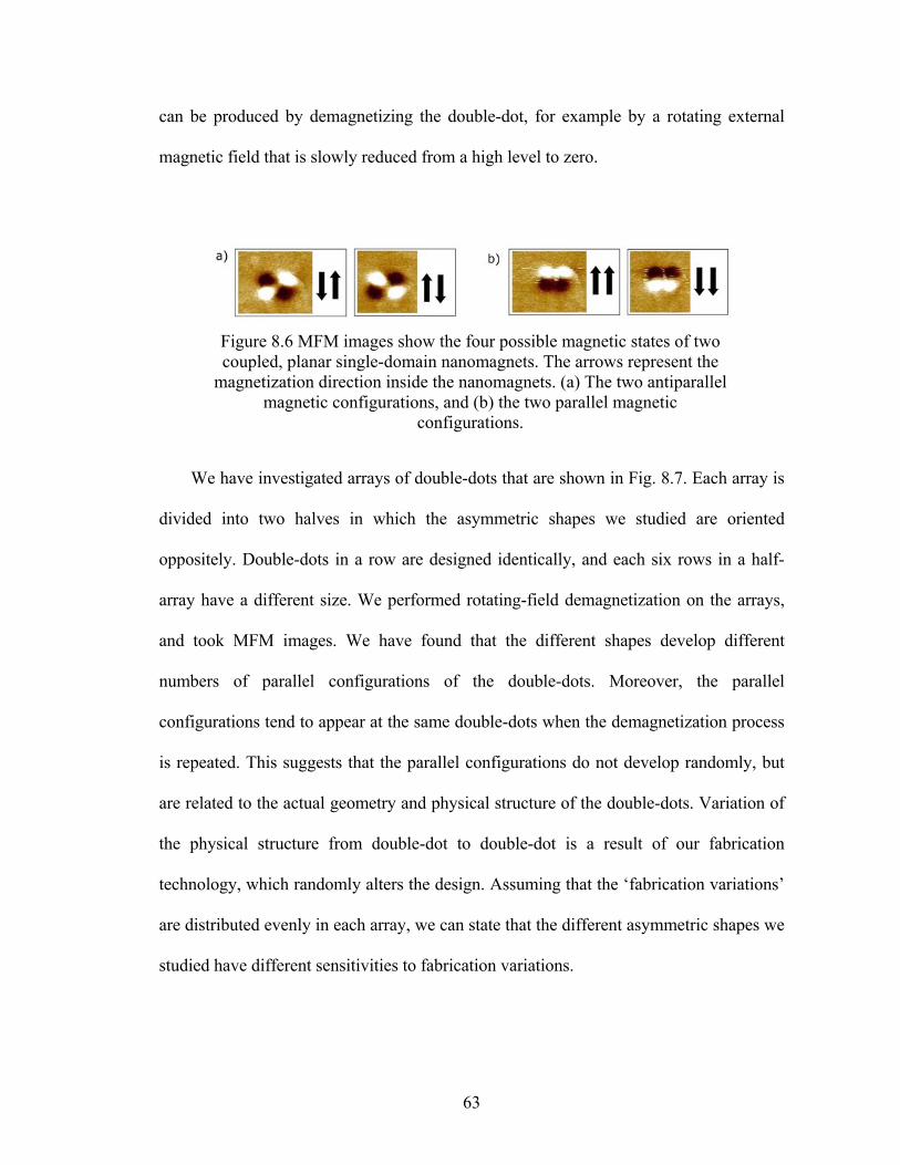
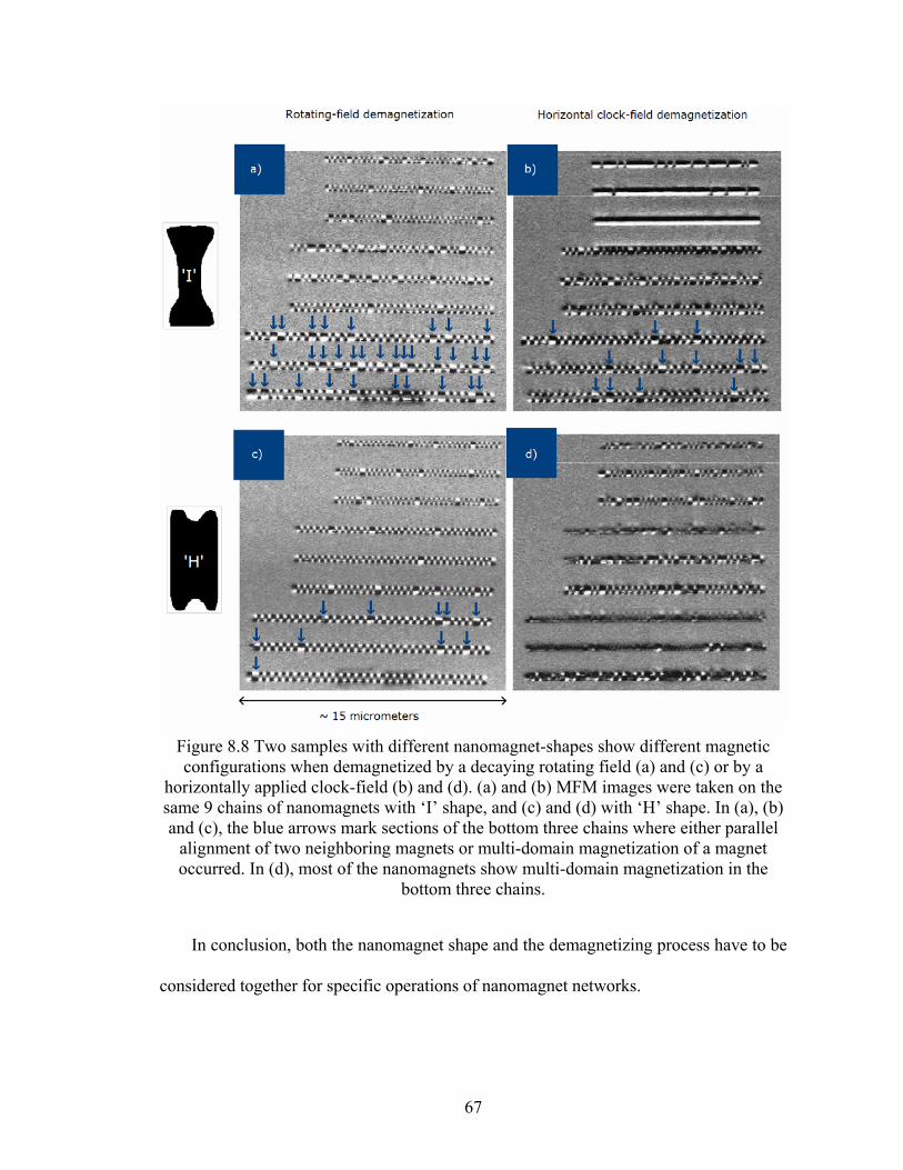
Embed Size (px)
Citation preview

EXPERIMENTAL STUDY OF NANOMAGNETS FOR MAGNETIC QUANTUM-
DOT CELLULAR AUTOMATA (MQCA) LOGIC APPLICATIONS
A Dissertation
Submitted to the Graduate School
of the University of Notre Dame
in Partial Fulfillments of the Requirements
for the Degree of
Doctor of Philosophy
by
Alexandra Imre MS
______________________________
Wolfgang Porod Director
______________________________
Gary H Bernstein Co-director
Graduate Program in Electrical Engineering
Notre Dame Indiana
April 2005
EXPERIMENTAL STUDY OF NANOMAGNETS FOR MAGNETIC QUANTUM-
DOT CELLULAR AUTOMATA (MQCA) LOGIC APPLICATIONS
Abstract
By
Alexandra Imre
Nanomagnets that exhibit only two stable states of magnetization can represent digital
bits Magnetic random access memories store binary information in such nanomagnets
and currently fabrication of dense arrays of nanomagnets is also under development for
application in hard disk drives The latter faces the challenge of avoiding magnetic
dipole interactions between the individual elements in the arrays which limits data
storage density On the contrary these interactions are utilized in the magnetic quantum-
dot cellular automata (MQCA) system which is a network of closely-spaced dipole-
coupled single-domain nanomagnets designed for digital computation MQCA offers
very low power dissipation together with high integration density of functional devices
as QCA implementations do in general In addition MQCA can operate over a wide
temperature range from sub-Kelvin to the Curie temperature Information propagation
and inversion have previously been demonstrated in MQCA In this dissertation room
temperature operation of the basic MQCA logic gate ie the three-input majority gate is
demonstrated for the first time
Alexandra Imre
The samples were fabricated on silicon wafers by using electron-beam lithography
for patterning thermally evaporated ferromagnetic metals The networks of nanomagnets
were imaged by magnetic force microscopy (MFM) with which individual
magnetization states were distinguished and mapped Magnetic dipole-ordering in the
networks was investigated in different samples Average ordering lengths were
calculated by statistical analysis of the MFM images taken after several independent
demagnetization processes
The average ordering length was found to be dependent on the shape and size of the
nanomagnets and limited by defects introduced during fabrication Defect tolerant
shape-design was investigated in samples of many different ring-shaped and elongated
nanomagnets The shape-effects were explained by means of micromagnetic
simulations
The majority gate was demonstrated by employing NiFe polycrystalline
nanomagnets with 70 nm x 120 nm lateral sizes Inputs were provided by additional
nanomagnets fabricated together with the gate and the operation was tested by MFM
The work presented here is an experimental proof of the MQCA concept The
theoretical calculations can be found in the dissertation of Gyoumlrgy Csaba
Gyoumlrgy Csaba ldquoComputing with field-coupled nanomagnetsrdquo PhD dissertation
University of Notre Dame 2004
1
CHAPTER 1
MOTIVATION
The magnetic quantum-dot cellular automata concept is a version of the field-
coupled QCA architecture that was first proposed in [1] The original idea was
introduced for a quantum dot system in which electrons tunnel between the quantum
dots under the influence of repelling Coulomb forces The basic QCA geometries and
their functions are shown in Fig 11 An elementary building block contains four
quantum dots in a square arrangement having one dot in each corner With two electrons
in the four-dot cell two stable states are defined by the configuration of the electrons as
they occupy the corners of the squares along the diagonals Electron tunneling occurs
only inside the cells and the neighboring boxes are coupled by long-range electrostatic
fields This architecture can propagate and process binary information when a feasible
clocking method is applied [2]
From a more general point of view the field-coupled QCA architecture is a signal
processing system built from simple identical bistable units that are locally connected to
each other solely by electromagnetic forces consequently the signal processing function
is defined by the placement of the building blocks and their physical interactions The
QCA concept can be realized in different physical systems
2
Figure 11 Quantum-dot cellular automata devices
The first experimental demonstration of a working electronic QCA cell was
published in 1997 [3] the logic gate in 1999 [4] and the shift register in 2003 [5] by the
same group at the University of Notre Dame In this approach the quantum dots are
realized by aluminum islands that are separated by a few-nanometer thick layer of
aluminum oxide Good agreement with the theoretical results was demonstrated at 50
mK Room temperature operation is expected only when the sizes are reduced to the
molecular scale [6] however the realization of molecular QCA requires more advanced
fabrication technology
We proposed to realize the QCA concept using ferromagnetic dots and magnetic
field coupling in 2002 [7][8] As an advantage compared to the above mentioned
electrostatic devices logic gates featuring single-domain magnets in the size scale of 100
nm are expected to operate at room temperature because of the relatively high energy
coupling energy
3
CHAPTER 2
MAGNETIC LOGIC DEVICES
Ferromagnetic materials have been considered for applications in digital computing since
the appearance of the first magnetic memory device As is very well summarized by
Hans Gschwind in his book ldquoDesign of digital computersrdquo published in 1967 [9]
ldquomagnetic components are rather attractive to the computer designer for several reasons
They possess an inherent high reliability
They require in most applications no power other than the power to switch their state
They are potentially able to perform all required operations ie logic storage and amplificationldquo
The key feature of such ferromagnetic components is magnetic hysteresis which
describes the internal magnetization of the components as a function of external
magnetizing force and magnetization history Hysteresis curves may take a variety of
different forms and many non-trivial aspects contribute to the picture of the underlying
physical mechanism A schematic hysteresis loop is shown in Fig 21
Nearly all applications rely heavily on particular aspects of hysteresis A number of
primary magnetic properties of a component can be determined from its hysteresis loop
The saturation magnetization is the magnetization value when magnetizing the material fully with a magnetizing force
4
The remanent magnetization or remanence is the magnetization value that remains in a material when the magnetizing force is zero The remanent magnetization is called retentivity when the material has been magnetized to the saturation point The level of residual magnetism may be lower than the retentivity value when the magnetizing force did not reach the saturation level
The coercive field or coercivity is the amount of reverse magnetic field that must be applied to a magnetic material to make the magnetic flux return to zero Soft magnetic materials have small coercive fields compared to other magnetic materials
The permeability (micro) is a property that describes the ease of establishing a magnetic flux in the component It is the ratio BH
B = micro0microRH = micro0(H+M) (21)
where B is the magnetic flux density vector (units 1T = 104 G) H is the magnetic field strength vector (units 1 Am = 4π10-3 Oe) M is the magnetization vector (units 1 Am = 10-3 emucm3) micro0 = 4π10-7 Hm is the permeability of free space and microR is the relative permeability
Figure 21 Magnetic hysteresis curve B vs H or M vs H is a
property of ferromagnetic materials
5
The field of magnetostatics was extensively studied in the last two centuries because
of the early applications of magnetic materials in simple machines The accumulated
knowledge then was able to provide magnetic components for the early stage of digital
computing
Prior to integrated circuit technology data in a computer was stored using magnetic
cores Cores were generally constructed by two methods The first called a tape wound
core was fabricated by wrapping a magnetic tape around a nonmagnetic toroidal form
The second called a ferrite core was made by molding finely ground ferrite (a ceramic
iron oxide) into a toroidal form Magnetic core memories were constructed by threading
current-carrying copper wires through the apertures of the cores and arranging the
approximately 1 mm diameter rings into an array Current pulses through the wires were
able to set the magnetization of the cores to clockwise or counter clockwise directions
which represented the binary information 0 and 1 The operation principle of the device
was similar to todayrsquos random access memories (RAM) The core memories became
widely used in computers by the early sixties but even after the rise of silicon they were
utilized in certain critical applications (for example NASA used ferrite core memories
until 1991) The cores were also investigated for logic applications A review can be
found in Gschwindrsquos book [9] page 460 The core is introduced as a magnetic amplifier
and logic gates and shift registers constructed from several cores are explained An
alternative physical variation of cores with additional apertures called a ldquotransfluxorrdquo is
also described The multi-aperture transfluxors were developed mainly by Hew Crane
working from the notion of controlling the direction of bit flow to achieve complete logic
capability Crane introduced the basic all-magnetic logic approach at the Fall Joint
6
Computer Conference in 1959 In 1961 the worlds first and only all-magnetic
computer with multi-aperture core logic system was demonstrated [10]
While magnetic cores are individual magnetic elements one can think of a
continuous magnetic medium that could host a whole memory or logic device if the
digital information were represented and conserved in restricted volumes of the medium
Such volumes can be uniformly magnetized regions called magnetic domains which are
separated from each other by regions where the magnetization vector rotates from the
magnetization direction of one domain to the other called domain walls The most
prominent domain walls the 180ordm Bloch and the 180ordm Neacuteel wall are depicted in Fig 22
The type of the domain walls as well as the preferred direction of the magnetic domains
depends on magnetic anisotropies of the actual material system
Figure 22 (a) Bloch wall (b) Neacuteel wall From
Hubert and Schafer [11] page 216
7
For instance in thin films with strong out-of-plane anisotropy magnetic stripe-
domains evolve spontaneously guided by energy minimization within otherwise
unstructured samples Such materials include garnets orthoferrites and hexaferrites
which were studied exhaustively for application in magnetic bubble technology
Magnetic bubbles are cylindrical domains of reversed magnetization in the thin film
Individual bubbles can be created in the film either by locally creating a vertical
magnetic field strong enough to reverse the magnetization or by spawning a secondary
bubble from a seed bubble Information can be represented then by the presence or
absence of ldquoisolatedrdquo bubbles or in a dense array of bubbles by different bubble ldquostatesrdquo
This was the main idea of the research on magnetic bubble memories in the late 60s [12]
Memory is provided here in that the bubbles persist as long as there is a static magnetic
field present and in that there is latitude in the magnitude of that field provides necessary
tolerances Bubbles can be propelled by creating a gradient in the bias field along the
film Bubbles move into the region of lower bias since the field is opposite to the bubble
magnetization and the magnetic energy decreases by the bubble movement The gradient
in the bias field can be created by current carrying conductors on the surface of the film
Continuous propagation can then be achieved by alternating pulses in an array of
conductors In most devices however propagation was done by coupling a rotating in-
plane field to a track of permalloy bars which came in a variety of shapes
Bubbles might also be used to perform logic but the storage application was more
obvious and was the only one that received significant attention
The scheme of propagating domain walls in a rotating external magnetic field is
employed by a contemporary research project as well Professor Cowburnrsquos group
8
previously at the University of Durham UK and presently at the Imperial College
London UK is working on specially designed loops of permalloy wires inside which
head-to-head and tail-to-tail domain walls are swept around [13][14] Logic functionality
is coded in the geometrical design of the wire loops
Finally another contemporary work that uses single-domain nanomagnets as basic
components should be mentioned The proposed architecture by Ney in [15] describes a
programmable logic element that is based on a single magnetic random access memory
(MRAM) cell It combines the inherent advantage of a non-volatile output with flexible
functionality that can be selected at run-time to operate as an AND OR NAND or NOR
gate This is an alternative approach to enhance computational power considering
magneto-electronic logic elements
In addition to such applications research in magnetic matter today focuses on
understanding dynamic processes on the nanoscale and engineering new materials with
special magnetic properties
9
CHAPTER 3
INTRODUCTION TO THE MAGNETIC QUANTUM-DOT CELLULAR
AUTOMATA (MQCA) CONCEPT
It already has been demonstrated that propagating magnetic excitations (domain walls
solitons) in magnetic nanostructures are suitable for digital signal processing [16][17]
According to our theoretical studies [7][8][18] nanomagnets with a sufficiently large
anisotropy low coercivity and a remanence equal to their saturation state may be utilized
practically as stray-field-coupled QCA building blocks In such a QCA block the digital
information is represented by the magnetization states of an individual nanomagnet just
as in magnetic random access memory (MRAM) [19] or patterned media hard disk drive
(HDD) [20] devices The number of stable magnetization states of a nanomagnet is
determined by its magnetic anisotropy for example crystalline or shape anisotropy The
nanomagnets are required to be magnetically bistable as shown in Fig 31(a) so that the
bit values lsquo0rsquo and lsquo1rsquo can be assigned to the two stable states
Consider an elongated-shape single-domain magnet that provides the hysteresis
curve sketched in Fig 31(a) This nanomagnet is strongly bistable as its remanent
magnetization (magnetization at zero external magnetic field) always points along the
long axis due to shape anisotropy Even though a magnetizing force can rotate the
magnetization away from the long axis when the force is removed the nanomagnet
switches to either of the two remanent states Placing many of these magnets side by side
10
along the long axis may result in an array of dipole-coupled nanomagnets that favor
antiparallel alignment of the magnetization directions This is due to the stray field of the
magnets acting on each other in close vicinity trying to magnetize their neighbors in the
opposite direction The antiparallel alignment that develops is called antiferromagnetic
ordering In MQCA this phenomenon drives the computation Figure 31(b) illustrates a
nanomagnet network in which the information propagates from left to right influenced
by the interface devices The network is driven by an external magnetic field into a
magnetic state that is allowed to relax to the antiferromagnetically-ordered ground state
The input and output of the nanomagnet network can be realized in a similar fashion to
an MRAM but the vast majority of the magnets (the interior of the array) is influenced
only by the field of their neighbors and need not be accessed externally
Figure 31 (a) Schematic hysteresis curve of an elongated nanomagnet
magnetization versus applied magnetic field both displayed along the longest axis of the magnetic particle (b) Illustration of a magnetic computing array The information flows from the input devices toward the output devices via
magnetic interactions
11
The field-coupled QCA devices are operated by an external clock a periodically
oscillating external magnetic field in our case which is able to drive the system into an
initial state and to control the relaxation to a ground state The calculated total
magnetostatic energy of two coupled single-domain permalloy nanomagnets as a
function of the magnetization direction of the right dot is shown in Fig 32(a) [18] The
magnetization of the left magnet is fixed The magnetostatic energy is dominated by
shape anisotropy of the elongated magnets which keeps the magnetization of the dots
bistable and results in two deep energy minima for magnetization directions parallel to
the magnetic easy axis (for 0ordm and for 180ordm) The ground state is found for 180ordm due to the
dipolar coupling which favors the antiparallel alignment while the parallel alignment is
found for 0ordm and represents a metastable state The energy difference between ground
state and metastable state is approximately 150 kT at room temperature and the energy
barrier from metastable to ground state is approximately 100 kT both are significantly
large for application at room temperature
The role of the external clock-field is to overcome the energy barriers between
metastable states and ground state Clocking can be performed by applying the magnetic
field along the short axis of the dots as explained in Fig 33 [8] In Fig 33(b) the
external field turns the magnetic moments of all magnets horizontally into a neutral logic
state later referred as ldquonullrdquo state against the preferred magnetic anisotropy This is an
unstable state of the system and when the field is removed the nanomagnets relax into
the antiferromagnetically ordered ground state as shown in Fig33(d) If the first dot of
the chain is influenced by an input device during relaxation then its induced switching
sets the state of the whole chain due the dipolar coupling To effect line switching the
12
input device must produce a local magnetic field that influences only the first
nanomagnet in the chain and which is oriented parallel with the long geometrical axis
This can be realized by a current carrying electrical wire for example as shown in Fig
33
Figure 32 Room-temperature energy diagram of two coupled
nanomagnets in the function of angle of magnetization of the right nanomagnet as against the fixed magnetization direction of the left
nanomagnet
13
Figure 33 Operating scheme of the nanowire (a) Initial configuration (b)
high-field state (ldquonullrdquo state) before and (c) after the application of the input (d) final ordered state [8]
One can think of this chain of coupled nanomagnets as an inverter chain Chains
containing an odd number of dots simply transmit the state of the input and those
containing even numbers of dots operate as an inverter The clock field affects the whole
chain thus all the inversions are done in one clock cycle This brings up the first
question that needs to be answered by experimental investigations ie is there a critical
length for these chains for which the antiferromagnetic ordering tends to be perfect
(errorless) If the answer is yes then is it large enough to support more complicated
arrangements of dots that work as a logic gate
14
CHAPTER 4
INVESTIGATION OF FABRICATION TECHNIQUES
The technology for fabricating arrays of nanomagnets is currently under development in
the HDD and MRAM industrial research
Patterned magnetic media are under consideration for used in HDDs to further
increase the areal density [20][21] Replacing thin-film media patterned media consist of
a regular array of magnetic nanoelements with uniaxial anisotropy The bits are stored in
the magnetization of the single domain nanoelements just as in the case of MQCA The
patterned media development is still at an early stage Fabrication techniques involve
electron-beam lithography (EBL) X-ray and interference lithography nanoimprinting
magnetic material deposition and pattern transfer The deposition of the magnetic
material is usually done by electroplating sputtering or evaporation the pattern transfer
applies reactive ion etching (RIE) or low-energy ion irradiation Focused ion beam (FIB)
techniques are also under consideration [22][23]
There is a significant effort directed toward fabricating nanomagnets with an easy
axis perpendicular instead of parallel to the surface and many papers present fabrication
of nanopillars [24] or patterning of metallic multilayers [25][26][27] which both
provide out of plane domain orientation
15
In addition to the research using the conventional fabrication techniques listed
above there is progress in self assembly of magnetic nanoparticles from colloidal
solution [28][29]
Finally there are some attempts to employ biomineralization of magnetic particles
as it can produce single and perfect crystals [30][31][32]
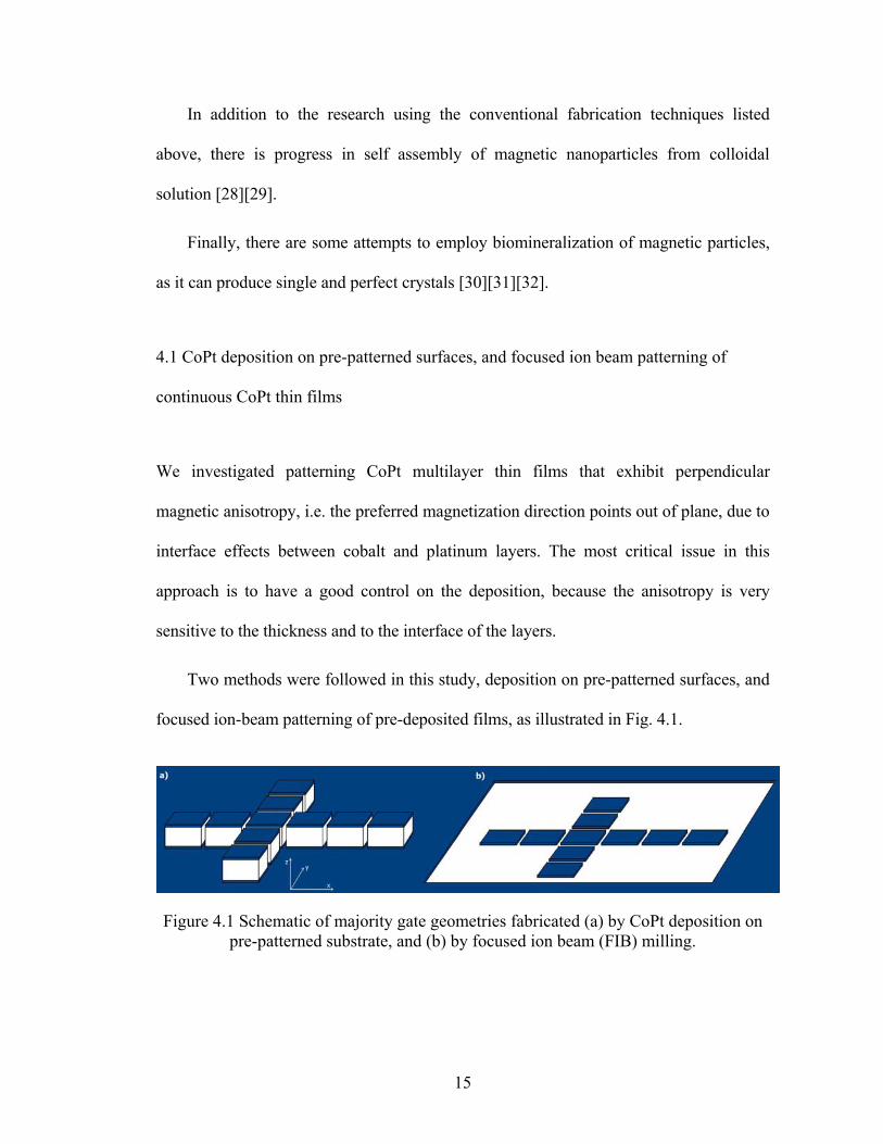
41 CoPt deposition on pre-patterned surfaces and focused ion beam patterning of
continuous CoPt thin films
We investigated patterning CoPt multilayer thin films that exhibit perpendicular
magnetic anisotropy ie the preferred magnetization direction points out of plane due to
interface effects between cobalt and platinum layers The most critical issue in this
approach is to have a good control on the deposition because the anisotropy is very
sensitive to the thickness and to the interface of the layers
Two methods were followed in this study deposition on pre-patterned surfaces and
focused ion-beam patterning of pre-deposited films as illustrated in Fig 41
Figure 41 Schematic of majority gate geometries fabricated (a) by CoPt deposition on pre-patterned substrate and (b) by focused ion beam (FIB) milling
16
In the case of deposition on pre-patterned surface the fabrication process was the
following
Define the pattern by EBL on PMMA (on SiO2 and on Si surfaces)
Create mask by Pt evaporation (35 nm) and lift-off
Transfer pattern by RIE (CF4 25 sccm O2 5 sccm 250 W chamber at 30 mTorr)
Sputter deposit CoPt (EMITECH K-675X sputter coater 910-3 mbar Ar plasma one cobalt and two platinum targets 200 mA co-deposition with rotating sample stage 36 rotations overall)
The approach to define fine patterns by high-resolution lithography and then to
transfer them into the substrate by RIE is described in [33] and [34] in the context of
patterned perpendicular magnetic media for data storage
The sputtering parameters in our case were optimized for largest domain size by
means of magnetic force microscopy (MFM) The sputtered magnetic deposit covers the
top of the islands the bottom of the trenches and to a lesser extent the sidewalls of the
islands Stripes of domains inside which the magnetization points out-of-plane were
found to form on the top of the islands while the anisotropy was destroyed in the
trenches where the surface was rough after the RIE as is seen in Fig 42(b) We could
not observe clear a single-domain magnetic configuration even for the smallest islands
(see Fig 42(d)) This might be because further reduction of the island size is required or
because the magnetic moments relax into the plane at the edges The effect of the
sidewall deposition is also questionable as it is exchange coupled to the top We
abandoned this fabrication method because answering these questions would require
more sophisticated methods such as very high resolution scanning electron microscopy
with polarization analysis (SEMPA)
17
Figure 42 (a) and (c) AFM (b) and (d) MFM images show the result of CoPt
deposition on pre-patterned silicon surface
For the other method we investigated we used a pre-deposited CoPt thin film
which was prepared at the IBM Almaden research center by Olav Hellwig alternating up
to 50 layers of sputter-deposited cobalt and platinum The hysteresis curves of this
sample which we measured by SQUID indicated strong perpendicular anisotropy
The focused ion-beam milling was done by a LEO 1540 Crossbeam microscope at
the Research Institute for Technical Physics and Materials Science in Budapest
Hungary with the following parameters Ga liquid-metal ion source 30kV acceleration
voltage 5-6 mm working distance 2-5 pA probe current 9-10 nm spot size Figure 43
shows a representative image of the patterned surface According to the MFM data
single-domain magnets were fabricated successfully However long range ordering on
the chains was not observed The accumulated dust from the milling process may have
disturbed the designed patterns since it appeared to be magnetic on the MFM images
generating a small contrast
18
Figure 43 (a) AFM and (b) MFM images show the result if FIB milling of CoPt
multilayer thinfilm
This work was presented in [35]
42 NiFe alloy and Co structures made by electron-beam lithography and lift-off
For the MQCA studies we fabricated our test samples by means of EBL thermal
evaporation and lift-off First poly-methyl-methacrylate (PMMA) was spun on the
surface of an oxidized silicon wafer PMMA is available in different solutions with
various molecular weights and widely used as a high contrast high resolution e-beam
resist [36] PMMA is a positive resist which undergoes chain scission and a reduction in
molecular weight with exposure to an electron-beam at normal doses of 300-500
microCcm2 The developer is strongly selective toward the dissolution of the low molecular
weight components of the resist The role of molecular weight and developer strength on
etch rate of PMMA was analyzed extensively by Greeneich [37] Generally a high
molecular weight material is chosen for high contrast and resolution performance In
order to improve the lift-off an additional co-polymer layer (a mixture of methyl
methacrylate and methacrylic acid) can be employed under the PMMA layer The resist
thickness that we use varies between 60 and 240 nm for the PMMA and between 150
19
and 550 nm for the co-polymer Pre-bake is done on a 175 ordmC hotplate for a few minutes
for each layer Figure 44 illustrates the steps of the fabrication process for both single
layer and double layer samples
Figure 44 Electron-beam lithography and lift-off technology process steps
(a) Exposure (b) metal deposition and (c) lift-off
The EBL was carried out on an AMRAY 1400 converted scanning electron
microscope driven by the Nanometer Pattern Generator System by J C Nabity [38]
Using a thermal emission tungsten cathode in the gun with 50 kV acceleration voltage
we have a lithography resolution of about 15-20 nm a minimum line width of 30-35 nm
and a minimum of 60-80 nm pitch To develop the exposed image we use a solution of
methyl-isobuthyl ketone (MIBK) isopropanol (IPA) and methyl-ethyl ketone (MEK)
1315 respectively which has been identified as a high contrast developer by
Bernstein et al [39] In Fig 44(b) the difference between the single layer and the double
20
layer resist is shown by the larger undercut in the co-polymer On the one hand this can
prevent the formation of thin walls along the border of the dots as seen in Fig 45(a) On
the other hand the patterns are less defined in the presence of the co-polymer because of
its larger shadow angle As a result the evaporated material that does not arrive perfectly
perpendicular to the surface of the substrate most of the time spreads out Another
property of the double layer resists is the development of PMMA bridges These bridges
appear to be quite elastic and can cause pattern deformation if they stick together before
evaporation as Fig 45(b) reveals We evaporated cobalt or permalloy as magnetic
material in an Airco Temescal FC1800 e-beam evaporator Both ferromagnetic materials
have a melting point of around 1750 K After evaporation the lift-off is done in a
mixture of methylene chloride (MC) and acetone (ACE) at a ratio of 81 respectively at
room temperature
Figure 45 Top view SEM micrographs after lift-off The elongated and flat
identically defined cobalt dots in the chains were fabricated (a) on single layer and (b) on double layer resist In case of single-layer resist there is material
accumulation of the edges of the elements In case of using double-layer resist the pattern can get deformed as the PMMA bridges stick together
21
The nanomagnets that can be fabricated by lift-off technique are necessarily planar
Building of pillar type nanomagnets which would have perpendicular anisotropy
due to their shape fails because of the closing of the PMMA windows as the evaporated
metal accumulates on the circumference If high aspect ratio pits are developed in the
resist the windows may close totally before the end of the deposition as it has happened
in case of the permalloy cones shown in Fig 46
Figure 46 Tilted SEM image of magnetic cones
fabricated by lift-off
The resolution of our e-beam lithography system is approximately 15-20 nm With
this resolution we can fabricate lines of approximately 30-35 nm wide and can place
elements approximately 20 nm apart at the closest but still separated Given this
resolution elements in the order of 100 nm can be fabricated with some control over the
shape
22
CHAPTER 5
PROPERTIES OF NANOMAGNETS
Magnetism at the nanoscale exhibits different physical phenomena than at macro scales
These phenomena arise because the physical size of the magnetic element is comparable
to or smaller than the characteristic magnetic length scales Many of the magnetic
characteristic length scales such as the domain size the domain-wall width the
exchange length or the thin-film perpendicular anisotropy threshold are ruled by energy
minimization Some others such as the spin diffusion length or the spin precession
length are the result of diffusion processes The magnetic phenomena that appear in
mesoscopic systems may be very diverse depending on the combination of the
characteristic length scales involved For an extensive review of characteristic length
scales see [40] from Dennis
51 Characteristic ferromagnetic material constants and the energy terms
Ferromagnets are characterized by intrinsic and extrinsic magnetic properties Intrinsic
properties such as Curie temperature (TC) saturation magnetization (MS)
magnetostriction (λS) and magneto-crystalline anisotropy (K1) are independent of
microstructure or nanostructure Extrinsic properties such as induced anisotropy (KU)
remanence magnetization (MR) or the coercivity field (HC) however derive from the
23
physical dimensions The design of nanomagnets for specific applications therefore
involves a careful selection of material and physical structure
The main intrinsic properties of the 3d metallic ferromagnetic elements such as
iron cobalt and nickel are collected in Fig 51 after Coey [41] The values refer to room
temperature
Structure
density (kgm3)
TC
(K)
MS
(MAm)
λS
(10-6)
K1
(kJm3)
A
(pJm)
lEX
(nm)
δBW
(nm)
Fe bcc
7874 1044 171 -7 48 83 15 41
Co hcp
8836 1388 145 -62 530 103 20 14
Ni fcc
8902 628 049 -34 -5 34 34 82
Figure 51 Characteristic constants of iron cobalt and nickel after Coey [41]
Each of the three elements has a different crystal structure namely body centered
cubic (bcc) for Fe hexagonal closely packed (hcp) for Co and face centered cubic for
Ni The crystal structure is responsible for the magneto-crystalline anisotropy K1
TC is the Curie temperature above which the material loses its magnetic long range
order and becomes paramagnetic
24
The magnetostriction parameter λS describes the change of a materialrsquos physical
dimension due to change in its magnetization The mechanical-strain-induced magnetic
anisotropy is related to σ the stress on the crystal by
KUSTRESS = (32)λSσ (51)
A is the exchange stiffness with which the exchange length lEX is derived as
2 SEX MAl deg= micro (52)
δBW is the width of the Bloch wall derived as
1 KABW =δ (53)
The intrinsic magnetic properties of the materials can be tailored by alloying
Permalloy is an fcc NiXFe1-X alloy with composition range 078ltXlt081 and it is
probably the best-studied soft magnetic material The particular feature of permalloy is
that K1 and λS change sign at nearly the same composition by chance which makes it
possible to achieve an excellent soft material with basically no intrinsic magnetic
anisotropy The main drawback of permalloy is its relatively weak polarization of micro0MS
asymp 10 T
Designing extrinsic properties of nanomagnets one needs to consider an energy
balance between exchange self-demagnetizing and anisotropy energies of the magnetic
body In summary the contributing energies are the following
The exchange energy is associated with quantum mechanical interactions among atomic moments that tend to align with each other in ferromagnetic materials
The self-demagnetizing or magnetostatic energy is associated with the potential energy per volume of the magnetization M in its own self-field
25
The anisotropy energy is associated with the tendency of the magnetic moments to align in certain directions Magnetic anisotropy can be exerted by a non-symmetric crystal structure or stress which both have an effect on electron spin-orbit coupling and crystal fields or it can be induced by the shape of the particle considering the self-demagnetizing effect at the boundaries
The magnetic domain and domain wall formation is the result of an energy balance
in the magnetic materials In magnetic materials that exhibit anisotropy the
magnetization within the domains points into one of the easy axis directions Figure 52
displays different magnetic domain structures that were made visible with the help of
polarization optics
Figure 52 Domains observed with magneto-optical methods on homogeneous magnetic
samples (a) Images from two sides of an iron whisker combined in a computer to simulate a perspective view (b) Thin film NiFe element (thickness 130 nm) with a weak transverse anisotropy (c) Faraday effect picture of domains in a single-crystal garnet film (bottom) with perpendicular anisotropy together with a schematic of the
magnetization (top) From Hubert and Schafer [11] page 1
26
52 Magnetic force microscopy (MFM) studies
Our technique to study magnetic nanostructures magnetic force microscopy (MFM)
provides close to the best magnetic spatial resolution available today However MFM
can obtain only steady-state magnetic images due to the scanning-probe approach We
use a multimode scanning probe microscope (SPM) that performs the full range of
atomic force microscopy (AFM) and scanning tunneling microscopy (STM) techniques
to measure surface characteristics including topography elasticity friction adhesion
and magneticelectrical fieldslowast Magnetic force microscopy is a secondary imaging mode
of the SPM and it is derived from tapping mode (TM) that is a patented technique (by
Veeco Instruments) TM maps topography by lightly tapping the surface with an
oscillating probe tip The cantileverrsquos oscillation amplitude changes with sample surface
topography and the topographic image is obtained by monitoring these changes and
closing the z feedback loop to minimize them
Dynamic MFM maps the magnetic force gradient (Fgrad) above the sample surface
This is performed through a two-pass technique ie the ldquoLift Moderdquo Lift Mode
separately measures topography and another selected property (magnetic force electric
force etc) using the topographical information to track the probe tip at a constant height
(lift height) above the sample surface during the second pass as illustrated in Fig 53
lowast Digital Instruments Nanoscope IV
27
Figure 53 MFM Lift Mode principles from DI support notes [42] (1amp2) Cantilever traces surface topography on first trace and retrace (3) Cantilever ascends to the lift
scan height (4amp5) Lifted cantilever profiles topography while responding to magnetic influences on second trace and retrace
We use standard and low-moment etched silicon MFM probes with a cantilever
length of 225 microm and a corresponding spring constant (cL) of approximately 1 Nm The
tip is coated with a ferromagnetic thin film and it can be viewed as a magnetic dipole
oriented in the z-direction because of its shape
While scanning the vibrating cantilever behaves to first approximation as a driven
harmonic oscillator and its equation of motion is
zFtfFzct
tzmF L gradz002
2
2cos)(++minus=
partpart
= π (54)
where m is the effective mass of the cantilever cL is the spring constant of the cantilever F0 is the driving force of the oscillation and Fzgrad is force gradient of a magnetic field acting on the tip in the direction of motion
⎟⎟⎠
⎞⎜⎜⎝
⎛
partpart
+part
part+
partpart
= 2
2
2
2
2
2
1
zHM
zH
MzH
MF zz
yy
xxgradz micro
(55)
This can be simplified if we assume the tip to behave as a magnetic dipole
(Mz gtgt Mx My)
28
In general every spatially varying force field changes the resonant frequency of the
cantilever In the case of our microscope the tip is driven to oscillate at a fixed
frequency and the MFM signal is the change of phase which is recorded as a function
of x y and z The recorded phase-shift of the cantilever oscillation is directly
proportional to the second derivative of the spatially varying magnetic force field In this
mode the amplitude is controlled to be constant Alternatively the amplitude could be
recorded and the phase could be kept constant
Figure 54 shows stray field of a single-domain magnet and the second derivative of
the stray field above the magnet at a particular distance calculated by Gyoumlrgy Csaba
The colors blue and red represent opposite signs Thus opposite poles of a magnet (ie
South and North) appear with opposite contrast on the MFM phase image (an image that
is constructed tracking the phase changes of the output signal)
Figure 54 Calculated stray field of a planar elongated magnet shown in a
vertical plane that cuts through the magnet (on the left) and calculated second derivative of the stray field in a plane above the magnet (on the right)
29
Figure 55 illustrates the topographic and the magnetic phase images of a single-
domain permalloy magnet The magnetic poles are clearly visible in Fig 55(b)
Figure 55 (a) Topography and (b) Lift Mode phase
images of a single-domain permalloy magnet
If the lateral magnetic resolution allows MFM can map the internal domain
structure of multi-domain magnets too For example see Fig 56 In this case the
contrast is generated by the stray field of domain walls Magnets with just slightly
different parameters or the exact same magnet after different magnetization processes
can exhibit different domain structures
In order to understand the dynamics of magnetic domain formation and to
confidently reconstruct magnetization states based on MFM images we use a popular
micromagnetic simulator called object oriented micromagnetic framework (OOMMF)
developed by the National Institute of Standards and Technology (NIST) Reconstructing
the magnetization from an MFM image is not straightforward The reconstruction
method is described in [43]
30
Figure 56 Topography and Lift Mode phase images of two micron-size permalloy
magnets
53 Micromagnetic simulator studies
OOMMF is a project of the Mathematical and Computational Sciences Division of the
Information Technology Laboratory at NIST in close cooperation with the
micromagnetic activity group (microMAG) of the Center for Theoretical and Computational
Materials Science at NIST OOMMF is package of portable extensible public domain
programs and tools for micromagnetics [44] The code forms a completely functional
micromagnetics package and also has a well documented flexible programmers
interface so that people developing new code can swap their own code in and out as
desired The main contributors to OOMMF are Mike Donahue and Don Porter
31
The core of the code is written in C++ with an open source scripting language
TclTk interface Target systems include a wide range of Unix and Windows platforms
The OOMMF applications communicate over Internet (TCPIP) connections in modular
architecture
The micromagnetic problem ie the geometrical description of a magnetic element
is impressed upon a regular 2D grid of squares with 3D magnetization spins positioned
at the centers of the cells For each cell the solver integrates the Landau-Lifshitz
equation
(56)
where M is the pointwise magnetization (Am) γ is the gyromagnetic ratio (m(As)) α is the damping coefficient (dimensionless) Heff is the pointwise effective field (Am) defined as
(57)
The average energy density E is a function of M specified by Browns equations
including crystalline anisotropy exchange self-magnetostatic (demagnetization) and
applied field (Zeeman) terms thus the effective field depends on the magnetization in a
very complex way partly through Maxwells equations and partly through
phenomenological forces which take into account quantum mechanical effects quasi-
classically The steady state solutions are usually complex domain patterns for larger size
bulk materials Apart from some very special cases the Landau-Lifshitz equation must
be treated numerically and for larger structures (gt5-10 microm) this becomes increasingly
time consuming
32
Figure 57 illustrates a 2D simulation in which the 3 nm cell size used is visible
Small asymmetries are introduced to the simulated shape when the bitmap file which is
used as an input is mapped onto the simulatorrsquos grid
Figure 57 Simulation of a nanomagnet in OOMMF [44]
Arrows in a figure of a simulation represent magnetization direction while the
coloring is assigned to one of the normalized vector components (ie x y or z) in each
cell
In addition to the description of geometry in a BMP file the simulator requests
characteristic material constants and external magnetic field description of the simulated
experiment Figure 58 shows the characteristic parameters that are used in our
simulations For the damping coefficient α a default value of 05 is set which allows
the solver to converge in a reasonable number of iterations Physical materials have α
typically in the range 00004 to 015 The anisotropy type is set to uniaxial in the plane
as we consider stable magnetization to point solely in the plane
33
Figure 58 Screen-shot of the characteristic parameters setting
As a further example we introduce the simulated hysteresis loop of the nanomagnet
that was already shown above in Fig 57 The hysteresis curve simulated in the direction
of the easy magnetic axis is displayed in Fig 59 In general at the microscale the
hysteresis curve tends to appear like a staircase where the steps correspond to sudden
transitions ie partial magnetization reversals At the nanoscale the magnetization
reversal can occur in a single step which results in a square-like hysteresis curve such
as shown in Fig 59
34
Figure 59 Simulated magnetization reversal along the easy axis of a
nanomagnet
Figure 510 displays the hysteresis loop simulated in the direction of the hard
magnetic axis
35
Figure 510 Simulated magnetization reversal along the hard axis of a
nanomagnet
Not only magnetization but magnetic fields can also be simulated by OOMMF
Figure 511 shows a study of stray field of a nanomagnet Outside the nanomagnet the
strongest stray fields occur at the close vicinity of the corners where they reach 250 mT
as is shown in Fig 511(b) At 10 ndash 15 nm away from the corner boundaries the
magnetic stray-field is still of the order of 100 mT as displayed in Fig 511(c) Stray
36
fields larger than 10 mT can be found everywhere around the nanomagnet within a
distance of approximately 50 nm as shown in Fig 511(d)
Figure 511 Simulated stray field of a nanomagnet (a) Magnetization of the
nanomagnet On the stray field images white areas correspond to magnetic fields higher than (b) 250000 Am (c) 100000 Am and (d) 10000 Am
The magnetic field values can be converted to induction by the SI equation B = micro0H
37
CHAPTER 6
MAGNETIC RINGS AND FLUX-CLOSURE MAGNETIC DOTS FOR QCA
Nanomagnets display well-defined domain patterns that evolve into each other at
specific applied fields The domain patterns can be designed by choosing proper shape
for the magnets Thus it is possible to design nanomagnet devices that show intended
functionality We demonstrate such functionality in the last chapter Both multi-domain
and single-domain structures however suffer from a relatively wide distribution of
domain nucleation fields which is referred to as the switching field distribution
Circular rings attracted special attention recently [45] due to the lack of strong stray
fields in their flux-closure states which ensures narrower switching field distribution
than for nanomagnets with sharp ends
61 Investigation of micron size square-rings
We investigated the static domain structures and the magnetization reversal processes of
square-rings Figure 61 (b) demonstrates a common magnetic state of such ring where
two oppositely lsquochargedrsquo domain walls are localized in the opposite corners
38
Figure 61 Micron size cobalt square-ring fabricated by e-beam lithography and lift-off sample is courtesy of Vitali Metlushko University of Illinois (a) SEM
(b) MFM image of the fabricated sample and (c) schematic drawing of the magnetization direction inside the ring that corresponds to the MFM image
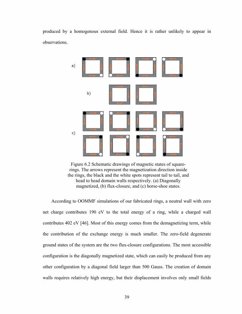
Domain walls can be either charged (when a net magnetization points inward or
outward at the corner) or neutral (when the magnetization simply lsquobendsrsquo at the corner)
By putting domain walls with positive negative or zero net volume charge to the
corners (and only to the corners) in all possible combinations we obtain a set of basic
domain configurations of square rings as summarized in Fig 62
We have fabricated permalloy square rings with a size of 21 microm x 21 microm 180 nm
wide and 25 nm thick and investigated domain-wall motion in them [46]
Micromagnetic simulations confirm the stability of the above introduced magnetic states
in our samples If no charged domain walls are present in a ring it displays a clockwise
or counterclockwise flux-closure magnetization distribution (see Fig 62(b)) The next
simplest configuration arrangement consists of two oppositely-charged walls The walls
may occupy either opposite (as shown in Fig 62(a)) or neighboring corners (Fig
62(c)) we will refer to the former as lsquodiagonally magnetizedrsquo and the latter as the
lsquohorse-shoersquo state Putting charged domain walls at all corners yields to a four-domain
configuration The four-domain state represents the highest energy and it cannot be
39
produced by a homogenous external field Hence it is rather unlikely to appear in
observations
Figure 62 Schematic drawings of magnetic states of square-
rings The arrows represent the magnetization direction inside the rings the black and the white spots represent tail to tail and
head to head domain walls respectively (a) Diagonally magnetized (b) flux-closure and (c) horse-shoe states
According to OOMMF simulations of our fabricated rings a neutral wall with zero
net charge contributes 190 eV to the total energy of a ring while a charged wall
contributes 402 eV [46] Most of this energy comes from the demagnetizing term while
the contribution of the exchange energy is much smaller The zero-field degenerate
ground states of the system are the two flux-closure configurations The most accessible
configuration is the diagonally magnetized state which can easily be produced from any
other configuration by a diagonal field larger than 500 Gauss The creation of domain
walls requires relatively high energy but their displacement involves only small fields
40
and energies Domain walls initially present in the structure can move and annihilate
each other forming other domain configurations MFM observations confirmed this
simple qualitative picture
We demonstrated switching between magnetic states in a controlled manner in [46]
also In order to gain control over the domain-wall displacements local fields should be
applied that overwhelm the effect of pinning-field distributions The simplest way to
accomplish this is to fabricate magnetic elements in close proximity to the square rings
such that the localized field of these nanoelements will be superimposed onto the
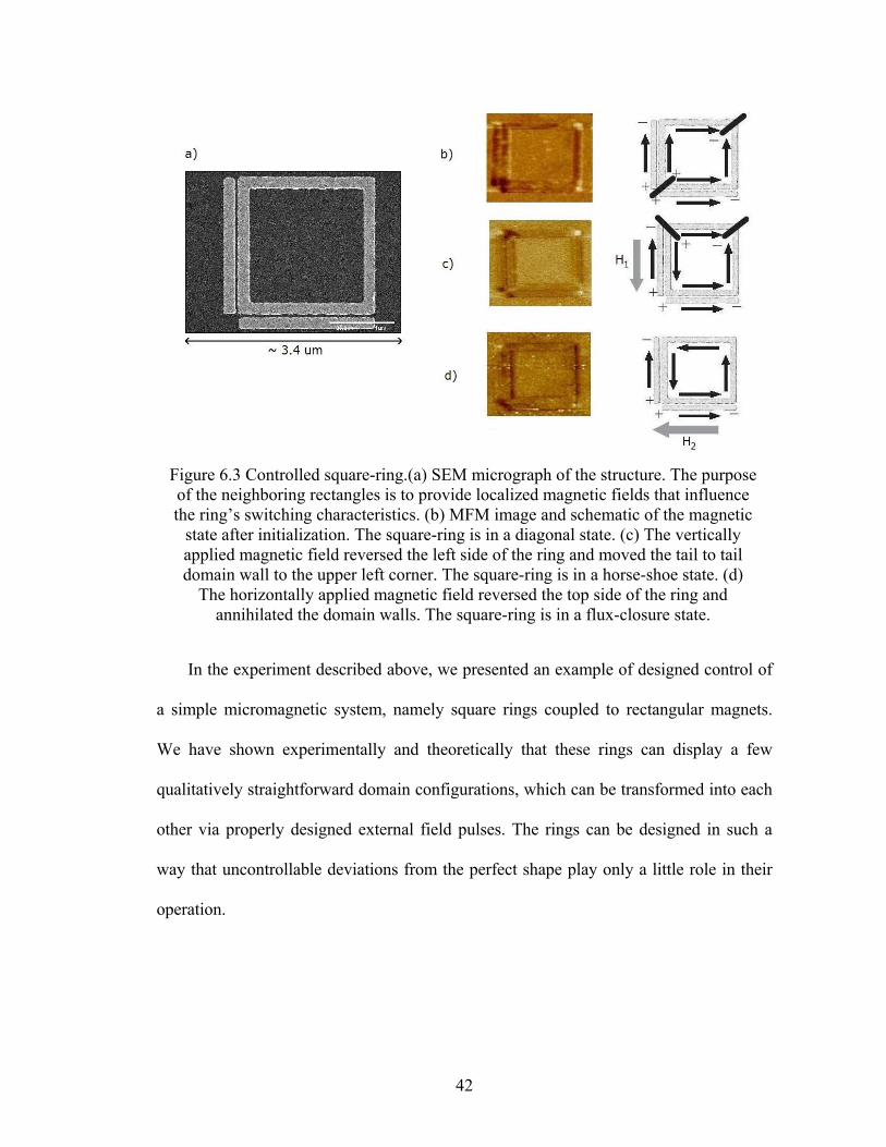
homogenous external field Figure 63(a) displays such a fabricated structure The
additional two rectangles were placed next to the ring with 40 nm separation After
magnetizing them along their longer axis the rectangular magnets stay in a simple and
stable single domain state with two oppositely-charged regions at their ends Simple
magnetostatic calculations show that the peak magnetic field generated by these
rectangles at the corners of the square rings is around 200 Gauss this value is definitely
larger than the switching-field variations of the lsquostand-alonersquo rings We estimate the
switching field of these rectangles (ie when their single-domain state is destroyed) to
be approximately 300 Gauss which is considerably larger than the value required for
domain-wall displacement in the square rings Hence their magnetization remains intact
during experiment and they act solely as a lsquodriverrsquo in this process providing well-
localized magnetic fields for the rings
The controlled switching process as recorded by MFM is illustrated in Fig 63(b)
(c) and (d) The initial state is a diagonally magnetized two-domain configuration with
the additional magnetic poles of the two uniformly magnetized rectangular elements
41
This state was produced by a 4600 Gauss diagonally-oriented external magnetic field As
a result there are three positively charged regions concentrated in the lower left corner in
Fig 63(b) Because of the demagnetizing effect of the additional poles the positively
charged domain wall of the ring is more mobile than the negatively charged domain wall
in the opposite corner In fact the positively charged domain wall can be displaced by a
130 Gauss external magnetic field which keeps the other domain wall intact Figure
63(c) shows the result of this step where the external field was applied vertically on the
structure As the left sidersquos magnetization reversed the ring switched to a horse-shoe
magnetic state At this point the positively charged domain wall is stabilized in the
upper left corner of the ring due to the negatively charged magnetic pole of the vertical
rectangular element In the last step a horizontally applied magnetic field is used to
reverse the top side of the ring During switching the positively and the negatively
charged domain walls annihilate each other and the ring relaxes to a counterclockwise-
rotating flux-closure domain configuration as seen in Fig 63(d) If opposite magnetic
fields were applied at each step (including the initialization) a clockwise field would
result The control elements determine which wall moves first and such control over the
final state would not be possible without these coupler elements
42
Figure 63 Controlled square-ring(a) SEM micrograph of the structure The purpose of the neighboring rectangles is to provide localized magnetic fields that influence the ringrsquos switching characteristics (b) MFM image and schematic of the magnetic
state after initialization The square-ring is in a diagonal state (c) The vertically applied magnetic field reversed the left side of the ring and moved the tail to tail domain wall to the upper left corner The square-ring is in a horse-shoe state (d)
The horizontally applied magnetic field reversed the top side of the ring and annihilated the domain walls The square-ring is in a flux-closure state
In the experiment described above we presented an example of designed control of
a simple micromagnetic system namely square rings coupled to rectangular magnets
We have shown experimentally and theoretically that these rings can display a few
qualitatively straightforward domain configurations which can be transformed into each
other via properly designed external field pulses The rings can be designed in such a
way that uncontrollable deviations from the perfect shape play only a little role in their
operation
43
62 Investigation of the flux-closure magnetic state in rings
As discussed earlier the degenerate ground states of magnetic rings are the two flux-
closure configurations If the relaxation process can be controlled by other relaxing rings
then a network of such rings can perform QCA operation with the digital bits lsquo0rsquo and lsquo1rsquo
being assigned to the two flux-closure states
The idea of storing binary information in magnetic rings comes from the era of
magnetic core memories for computers in the early sixties Even after the rise of silicon
ferrite cores of a size of a millimeter in diameter were utilized in certain applications [9]
At a thousand times smaller size ring-like designs are attractive due to their low
switching-field distribution compared to other submicron geometries Narrow circular
rings were found to possess two types of stable magnetic states polarized so-called
onion states (field lines split around the center in opposite directions with head-to-head
and tail-to-tail domain walls at opposite sides) and totally flux-closed vortex states with
clockwise and counterclockwise rotation (field lines encircle the center) Zhu et al [47]
proposed to use the chiralities of the vortex states (the rotation direction of
magnetization) in circular rings as the carriers of information for data storage
Micromagnetic simulations show that wide rings compared to the earlier-
investigated narrow rings support only the two flux-closure magnetic states in
remanence which makes them eligible for implementing bistable switches Figure 64
summarizes the simulated remanent states of an in-plane magnetized 800 nm outer
diameter ring with varying width In the case of the narrowest ring in Fig 64(a) the
remanent state is the onion state In wider rings (with large outer and inner circle
44
diameter ratio) the domain walls are expected to undergo a transition from a transverse
domain wall of head-to-head domains to a local vortex structure This transition was
predicted by McMichael and Donahue [48] for the case of magnetic strips The formed
vortex cores can provide a stable magnetization as shown in Fig 64(b) However if the
vortex cores are not constrained by local shape anisotropy they can move along and be
annihilated on the borders and as a result wide rings are able to relax to flux-closure
remanent state as the external field is removed (Fig 64(c)) This work was presented in
[49]
Figure 64 OOMMF simulation of remanent states as a result of
relaxation from fully magnetized state in plane (a) onion state (b) vortex-core state and (c) flux-closure state
For providing flux-closure magnetic states in remanence thus the magnetic element
has to be either a wide ring or a disk
45
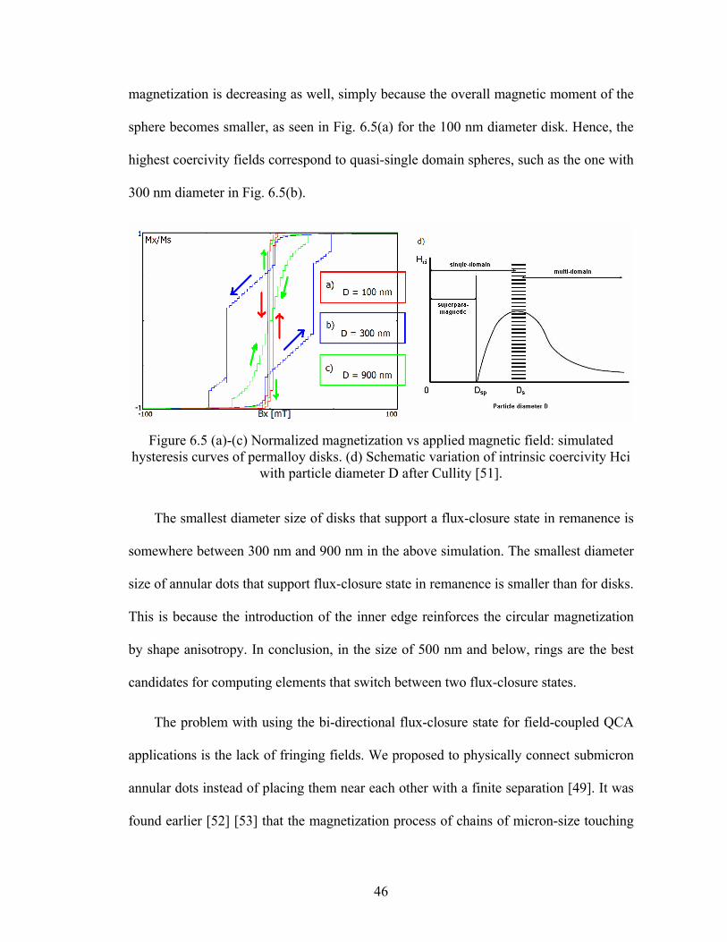
However for the disk-shape element the flux-closure magnetization can be
maintained only if the element is sufficiently large When the disk diameter is reduced
the exchange energy becomes comparable to the magnetostatic energy and the disk
becomes single domain Different hysteresis curves that show different switching
behavior for various disk sizes were measured by Cowburn [50] In Fig 65 we show
simulated hysteresis curves for permalloy disks with 10 nm thickness in three sizes 900
300 and 100 nm diameters The external magnetic field is applied in the x direction in
the plane of the disks A 100 mT applied field can completely saturate the disks in the
direction of the field As the field is reduced reversed and increased to 100 mT to the
opposite direction the 300 nm and the 900 nm disks switch their magnetization through
a vortex domain structure while in the 100 nm diameter disk the elementary magnetic
moments rotate around coherently which is called single-domain behavior In Fig 65(d)
ranges of single-domain and multi-domain magnetic behavior of the spherical geometry
are given as a function of sphere diameter (D) after Cullity [51] Particles with diameters
close to DS are between the single-domain and the multi-domain region and can be
referred as quasi-single domain magnets Quasi-single domain particles have single
domain remanent state but the magnetization reversal occurs through domain wall (ie
vortex-core) formation propagation and annihilation The formation of the vortex-core
takes a relatively large amount of energy that is provided by the external field As the
particle size is increased into the multi-domain region the magnetostatic energy
overcomes the exchange term and domain wall(s) will exist already in the remanent
state This is the case with the 900 nm diameter disk in Fig 65(c) With decreasing
particle size in the single-domain region the external field that required flipping the
46
magnetization is decreasing as well simply because the overall magnetic moment of the
sphere becomes smaller as seen in Fig 65(a) for the 100 nm diameter disk Hence the
highest coercivity fields correspond to quasi-single domain spheres such as the one with
300 nm diameter in Fig 65(b)
Figure 65 (a)-(c) Normalized magnetization vs applied magnetic field simulated
hysteresis curves of permalloy disks (d) Schematic variation of intrinsic coercivity Hci with particle diameter D after Cullity [51]
The smallest diameter size of disks that support a flux-closure state in remanence is
somewhere between 300 nm and 900 nm in the above simulation The smallest diameter
size of annular dots that support flux-closure state in remanence is smaller than for disks
This is because the introduction of the inner edge reinforces the circular magnetization
by shape anisotropy In conclusion in the size of 500 nm and below rings are the best
candidates for computing elements that switch between two flux-closure states
The problem with using the bi-directional flux-closure state for field-coupled QCA
applications is the lack of fringing fields We proposed to physically connect submicron
annular dots instead of placing them near each other with a finite separation [49] It was
found earlier [52] [53] that the magnetization process of chains of micron-size touching
47
rings displays a clear anisotropy For applied magnetic fields perpendicular to the chain
direction the switching occurs pair-wise For fields applied parallel to the chains the
switching of the edge ring element triggers the switching process and extended sections
of the chains were found to switch simultaneously In these sections neighboring rings
display vortices of alternating chirality similar to the interlocking gears in gear trains as
shown in Fig 66(b) A chain of touching rings switching into alternating vortex states
can be seen as an inverter chain and represents the basic digital computation
Figure 66 MFM image and schematic magnetization of (a) onion states and (b)
flux-closure states of two exchange-coupled 250 nm wide 25 nm thick permalloy rings (contrast in flux-closure state is due to magnetic ripples)
However with the application of touching (ie exchange-coupled) rings we are
outside of the focus of this dissertation on field-coupled QCA architectures
48
CHAPTER 7
DIPOLAR COUPLING OF SINGLE-DOMAIN NANOMAGNETS
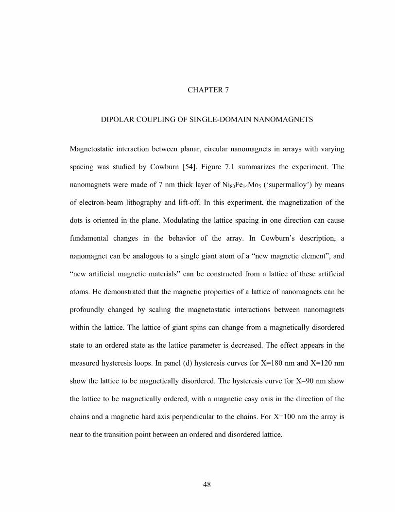
Magnetostatic interaction between planar circular nanomagnets in arrays with varying
spacing was studied by Cowburn [54] Figure 71 summarizes the experiment The
nanomagnets were made of 7 nm thick layer of Ni80Fe14Mo5 (lsquosupermalloyrsquo) by means
of electron-beam lithography and lift-off In this experiment the magnetization of the
dots is oriented in the plane Modulating the lattice spacing in one direction can cause
fundamental changes in the behavior of the array In Cowburnrsquos description a
nanomagnet can be analogous to a single giant atom of a ldquonew magnetic elementrdquo and
ldquonew artificial magnetic materialsrdquo can be constructed from a lattice of these artificial
atoms He demonstrated that the magnetic properties of a lattice of nanomagnets can be
profoundly changed by scaling the magnetostatic interactions between nanomagnets
within the lattice The lattice of giant spins can change from a magnetically disordered
state to an ordered state as the lattice parameter is decreased The effect appears in the
measured hysteresis loops In panel (d) hysteresis curves for X=180 nm and X=120 nm
show the lattice to be magnetically disordered The hysteresis curve for X=90 nm show
the lattice to be magnetically ordered with a magnetic easy axis in the direction of the
chains and a magnetic hard axis perpendicular to the chains For X=100 nm the array is
near to the transition point between an ordered and disordered lattice
49
Figure 71 Scanning electron micrographs of some of the nanomagnet lattices studied by Cowburn [54] Each nanomagnet is of 60 nm diameter and has a y-direction lattice parameter of 180 nm The x-direction lattice parameter is (a)
180 nm (b) 110 nm and (c) 90 nm In (d) measured hysteresis loops for different lattice spacing (X) and applied field directions All loops were measured within the field range plusmn150 Oe the large panels show high-
magnification views around zero field insets show the full measured loop The vertical axis of all loops is magnetization normalized by the saturation value
Cowburnrsquos experiment examined magnetostatic coupling between the nanomagnets
(especially but not exclusively between nearest neighbors) which becomes stronger as
the separation of the dots (X) is reduced This is directly analogous to the onset of
ferromagnetism in an atomic lattice
50
The lesson is the following in the case of interacting arrays the magnetic ground
state of the magnets can be different from their isolated ground state If the magnets are
placed close to each other in the array the coupling between them will be strong and the
array will exhibit the collective behavior of the magnets
The evidence that networks of interacting submicrometer magnetic dots can be used
to perform logic operations and to propagate information at room temperature was
demonstrated by Cowburn in 2000 [16] The QCA concept was applied to nanomagnets
for the first time in this work
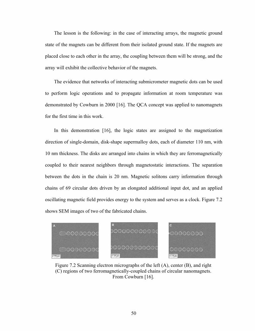
In this demonstration [16] the logic states are assigned to the magnetization
direction of single-domain disk-shape supermalloy dots each of diameter 110 nm with
10 nm thickness The disks are arranged into chains in which they are ferromagnetically
coupled to their nearest neighbors through magnetostatic interactions The separation
between the dots in the chain is 20 nm Magnetic solitons carry information through
chains of 69 circular dots driven by an elongated additional input dot and an applied
oscillating magnetic field provides energy to the system and serves as a clock Figure 72
shows SEM images of two of the fabricated chains
Figure 72 Scanning electron micrographs of the left (A) center (B) and right (C) regions of two ferromagnetically-coupled chains of circular nanomagnets
From Cowburn [16]
51
The experimental setup was the following the chains are inspected by magneto-
optical measurement based on the longitudinal Kerr effect This is done by measuring
the polarization state of a reflected linearly-polarized laser beam that is focused on the
chains The plane of incidence of the light is set to lie along the length of the chains The
laser spot covers almost the entire 9-mm length of the networks and so the recorded
signal is a measure of the total component of magnetization lying along the chain of dots
and once correctly calibrated is a measure of the number of dots switching in a network
The elongated input dots are set by applying a single magnetic field pulse of either +300
Oe (for a logic 1) or -300 Oe (for a logic 0) directed along the chain of dots A weak
oscillating magnetic field of plusmn25 Oe amplitude and 30 Hz frequency combined with a
-10 Oe bias magnetic field is then applied along the chain of dots The magneto-optical
signal from the networks is recorded over several cycles
It was found that almost the entire chain of 69 dots is switching as the solitons
sweep along the chains
A computational study using the LandaundashLifshitz magnetization dynamics into the
dynamic properties of a magnetic soliton on a chain of above described single-domain
nanomagnets was published in [50] by Cowburn A simulation result is shown in Figure
73 that predicts a possible uniform soliton velocity of approximately 1000 ms and a
nanomagnet reversal time of 240 psec
52
Figure 73 Calculated evolution of a soliton propagating along a chain of coupled
nanomagnets under the action of a 30Oe field applied from left to right in x-direction and the calculated propagation speed of the soliton as a function of applied field
strength
We have seen that ferromagnetically-coupled disk-shape nanomagnets can be
applied in QCA-type systems
Single-domain circular nanomagnets with additional uniaxial anisotropy transverse
to the chains show more complex behavior as summarized in Fig 74 after Cowburn
[55] The three simplest configurations are considered here ferromagnetic lateral (FL)
ferromagnetic transverse (FT) and antiferromagnetic transverse (AFT) The energy of
each configuration U consists of two terms uniaxial anisotropy energy (KU) and dipolar
coupling energy (J)lowast
If the uniaxial anisotropy is weak then the most favorable configuration is the
ferromagnetic lateral The uniaxial anisotropy has to be larger than J for
antiferromagnetic ordering of the magnetic moments to occur
lowast J is defined here as the dipolar coupling energy between two antiparallel magnets
53
Figure 74 Ferromagnetic transverse (FT) antiferromagnetic
transverse (AFT) and ferromagnetic lateral (FL) configurations of single-domain disk-shape nanomagnets with uniaxial anisotropy transverse to the chain (after Cowburn [55])
Slightly elongated supermalloy nanomagnets with sizes of 100 nm x 120 nm and
with thickness of 10 nm were shown by Cowburn in [55] to prefer the antiferromagnetic
transverse configuration Representative chains of the fabricated sample can be seen in
Fig 75(a) (b) (c) and (d) An alternating and decaying external magnetic field
transverse to the chains was used for demagnetization and the final magnetization of the
chains was checked by magneto-optical Kerr measurements The largely elongated
nanomagnet at the left end of the chains was used as an input as their magnetization
remained intact during the demagnetization process The experimentally determined
antiferromagnetic ordering parameter measured for different numbers of nanomagnets
(n) in the chains is plotted in Fig 75(e) From this plot the antiferromagnetic ordering
length was found to be 4 or 5 nanomagnets This relatively small number was explained
by a frustration-propagation model in which the ordering process was claimed not to be
well supported by the external demagnetizing field unlike in the case of the
ferromagnetically-coupled circular dots introduced earlier
54
Figure 75 Antiferromagnetically-coupled chains of (a) one (b) two (c) five and (d)
seven nanomagnets fabricated by Cowburn [55] (e) Experimentally determined ordering parameter as a function of nanomagnet-number (n) in the chains
As we will show in the next chapters the antiferromagnetic ordering length indeed
can be improved by choosing an appropriate demagnetizing method and by introducing
more complex nanomagnet shapes
55
CHAPTER 8
SHAPE ENGINEERING OF NANOMAGNETS
The shape design of the nanomagnets is a very important part of this study because the
shape anisotropy that we introduce to the dots is the one mainly responsible for the
switching dynamics when interplaying with the external clock-field and the stray field of
the neighboring dots If the switching dynamics can be controlled then the most
fundamental requirement of the MQCA systems will be satisfied ie each elementary
building block will operate reliably
81 Investigation of the quasi single-domain size
As we have seen before nanomagnets have four ranges of volume size
superparamagnetic true single-domain quasi single-domain and multi-domain sizes
Nevertheless these ranges cannot be unambiguously determined for a given
ferromagnetic material due to the strong influence of the shape stress and crystalline
anisotropies on the domain structure
For a simple demonstration of the effect of shape we have fabricated samples of
differently shaped and sized permalloy elements After demagnetization the samples
were imaged by MFM with no external field present Figure 81 shows 4 x 12 arrays of
elliptical rectangular and triangular shapes In the four rows the lengths of the elementsrsquo
56
vertical axes are 2 3 4 and 5 microm In the 12 columns the lengths of the elementsrsquo
horizontal axes vary between 450 nm and 3 microm The thickness of the evaporated
permalloy is 25 nm The separation between the elements is more than a micron so it is
assumed that the coupling between them is negligible
On the left side of the rows the elements are in the single-domain magnetic state as
only two strong contrast dark and bright spots can be seen for each (except the first row
of Fig 81(b)) The spots correspond to the magnetic South and North poles Along the
rows to the right the length of the horizontal axis of the elements is increasing and at
some point the single-domain configuration is replaced by a multi-domain
configuration In multi-domain state the MFM contrast is generated by the domain
walls The elliptical shapes develop two the rectangular shapes develop four while the
triangular shapes develop three domains in the multi-domain states of these samples
Note that the number of domains can be increased for the same patterns if the thickness
of the elements (ie the third dimension) is increased
Looking at the columns however the increasing length of the vertical axis ensures
the single-domain configuration Even though the additional volume increases the
magnetostatic energy of an element which tends to break up the magnetization
configuration into domains the anisotropy of the elements is also increased and has a
stronger effect This because the elementary moments at the boundary of the magnets
align with the edge of the body (shape anisotropy) In fact it is the aspect ratio between
the length of the two lateral axes that matters as mentioned by Zhu et al [56]
57
Figure 81 MFM images of arrays of differently shaped planar
permalloy magnets in various sizes The red lines mark the transition between single-domain and multi-domain remanent state The green
lines mark the two elements with 11 aspect ratio of axes in each array
58
Another important observation is that the pointed ends of the elongated elements
like for the elliptical or for the triangular shapes can also encourage the single-domain
state
Due to our limitations in lithography resolution the majority of our studies were
done on quasi single-domain nanomagnets with around 100 nm width At this size we
found that an aspect ratio (lengthwidth) of 2 is sufficient to ensure single-domain
remanence Wider magnets might need larger aspect ratio unless their ends are pointed
Note that closely spaced nanomagnets can show ordering in their magnetic patterns
even if they develop multi-domain configuration in remanence See Fig 82 for example
Figure 82 Multi-domain closely spaced
cobalt dots show ordering in their magnetic pattern (a) AFM and (b) MFM
image of a 10-dot long chain
82 Effects of shape on the magnetization reversal of quasi single-domain nanomagnets
Elongated triangular elements are especially interesting due to their asymmetry on
the magnetic easy axis The assymetry can provide different sensitivity to local fields on
the two different sides which for example can define a preferred direction of the
antiferromagnetic ordering process in a chain of such dots From our viewpoint of
MQCA this is equal to rectified signal propagation along the chain Our simulations
59
show such a phenomenon however we did not have an appropriate experimental setup
with which to confirm the dynamics
Figure 83 demonstrates the relaxation of pairs of nanomagnets one with an
asymmetric trapezoid shape and one with a symmetric rectangle shape The coupling is
through an approximately 10 nm separation between the magnets in both pairs A
horizontal external field of 200 mT is applied on the pairs in Fig 83(a) and (b) which
forces the magnetization to point along the hard axis of the nanomagnets The rectangles
are almost uniformly magnetized under this field except at the lsquoouterrsquo corners where the
magnetization is slightly pinned The lsquoinnerrsquo corners (the corners that are next to the
other magnet) are not pinned because the elementary magnetic moments at the boundary
of the two magnets couple ferromagnetically As the external field is removed from the
rectangle-shaped dots in Fig 83(d) (f) and (h) the two magnets switch together as if
onersquos magnetization would be a mirrored image of the otherrsquos In contrast the two
trapezoids show different relaxation dynamics The reason is that the two sharp corners
are on the lsquoinnerrsquo side of the pairs for the nanomagnet on the left while they are on the
lsquoouterrsquo side for the nanomagnet on the right The corners on the lsquoouterrsquo side are pinned
more strongly As the external field is removed in Fig 83(c) (e) and (g) the more
weakly pinned nanomagnet on the left starts the switching and induces the final state of
the nanomagnet on the right
60
Figure 83 Simulated relaxation of coupled pairs of two trapezoid-shape and
two rectangle-shape permalloy nanomagnets The color is coded to the normalized magnetization vectorrsquos vertical component (My) and the arrows
point in the direction of the local magnetization
Note that when the external clock-field is oriented along the magnetic hard axis
assymetry introduced in shape on the magnetic easy axis can possibly enhance the
performance of nanomagnet networks However assymetry in shape on the magnetic
hard axis may not be allowed to avoid preferential magnetization switching that would
be introduced by the external field
61
We performed an experimental shape study by investigating chains of
antiferromagnetically-coupled permalloy nanomagnets in the sizes of 75 95 and 125 nm
for the short axes and three aspect ratios of 2 25 and 3 These magnets exhibit a
magnetic easy axis along the direction of their long axis As a general rule we found that
shapes with well-defined nucleation sites (ie sharp corners) for domain walls can
control magnetic domain formation during magnetization reversal making the switching
process more predictable and resulting in longer correlation lengths in arrays of coupled
nanomagnets [57] In other words switching-field variations that arise from fabrication
variations like the imperfect shape or rough surface of the dots may be overcome to
some extent by means of fault-tolerant shape design For a representative example of the
idea of fault-tolerant design see Fig 84 In this shape the pointed corners focus the
magnetrsquos stray-field
Figure 84 Coupled planar nanomagnets with sharpened corner (a) Simulated stray field
of two coupled dots and (b) SEM image of a corresponding chain of permalloy dots
Corners can also be used to ensure single-domain remanent magnetization for
nanomagnets with lower aspect ratio In Fig 85(b) and (d) MFM images of chains of
cornered and rounded nanomagnets are introduced Each MFM image shows three
62
chains of 64 dots The width of the dots is 125 nm in each chain while the aspect ratio of
the nanomagnets is 2 for the top chain 25 for the middle chain and 3 for the bottom
chain SEM images of the bottom chains are shown in Fig 85(a) and (c) The MFM
images were taken after demagnetization of the samples As seen in Fig 85(b) in case
of the rounded shape even the aspect ratio of 3 was not sufficient to keep every
nanomagnet in the bottom chain single-domain On the contrary for the cornered
rectangular shape the aspect ratios 3 and 25 were both sufficient
Figure 85 Study of two different shapes (a) and (c) are SEM images of a section of the
investigated chains with the highest aspect ratio nanomagnets (b) and (d) are MFM images of three 64-dot long chains with different aspect ratio nanomagnets
Being much simpler systems than the chains we fabricated and studied pairs of
coupled nanomagnets which we refer to as double-dots Double-dots have four possible
magnetic configurations assuming that the nanomagnets are single-domain An applied
magnetic field along the longer axis of the nanomagnets can set both domains parallel as
shown in Fig 86(b) This is a metastable state of the double-dot In the ground state the
magnetization of the domains is antiparallel due to the dipole coupling The ground state
63
can be produced by demagnetizing the double-dot for example by a rotating external
magnetic field that is slowly reduced from a high level to zero
Figure 86 MFM images show the four possible magnetic states of two coupled planar single-domain nanomagnets The arrows represent the
magnetization direction inside the nanomagnets (a) The two antiparallel magnetic configurations and (b) the two parallel magnetic
configurations
We have investigated arrays of double-dots that are shown in Fig 87 Each array is
divided into two halves in which the asymmetric shapes we studied are oriented
oppositely Double-dots in a row are designed identically and each six rows in a half-
array have a different size We performed rotating-field demagnetization on the arrays
and took MFM images We have found that the different shapes develop different
numbers of parallel configurations of the double-dots Moreover the parallel
configurations tend to appear at the same double-dots when the demagnetization process
is repeated This suggests that the parallel configurations do not develop randomly but
are related to the actual geometry and physical structure of the double-dots Variation of
the physical structure from double-dot to double-dot is a result of our fabrication
technology which randomly alters the design Assuming that the lsquofabrication variationsrsquo
are distributed evenly in each array we can state that the different asymmetric shapes we
studied have different sensitivities to fabrication variations
64
Figure 87 Repeated rotating-field demagnetizations of double-dot arrays reveal that different shapes can show different sensitivity to fabrication variations The parallel
magnetic configurations (and configurations with multi-domain states) are underlined with red if they appear as a result of both independent demagnetizations at the same double-dot The rest of the parallel magnetic configurations (and configurations with
multi-domain states) are underlined with blue
65
In addition to the nanomagnet-shape dependence of the magnetic configuration of a
coupled system in ground state we also found a dependence on the demagnetization
process Figure 88 illustrates an experiment in which chains of two different shapes
were demagnetized by using two different demagnetizing methods The MFM images
were taken on 9 chains of 64 antiferromagnetically-coupled permalloy nanomagnets with
sizes of 75 95 and 125 nm for the short axes and three aspect ratios of 2 25 and 3 for
each width To compare the performance of the lsquoIrsquo- and the lsquoHrsquo-shaped nanomagnets
see the bottom three chains with 125 nm magnet-width first The blue arrows mark
sections of the bottom three chains where either parallel alignment of two neighboring
magnets or multi-domain magnetization of a magnet occurred These are lsquoerrorsrsquo of the
antiferromagnetic ordering In the case of rotating-field demagnetization there are 8 14
and 10 lsquoerrorsrsquo in Fig 88(a) for the aspect ratios 2 25 and 3 respectively This gives an
average of 106 lsquoerrorsrsquo in the inspected chains which results in an approximate average
ordering length of 6 nanomagnets by simply dividing the whole length of 64 by 106
While this calculation results in an approximate average ordering length of 6
nanomagnets for the 125 nm wide lsquoIrsquo shapes it gives an average ordering length of 19
for the 125 nm wide lsquoHrsquo shapes This is a remarkable difference Repeated independent
rotating-field demagnetization of the samples produced similar results However when
applying horizontal clock-field on the chains the lsquoerrorsrsquo appear in different number
While the average ordering length of the 125 nm wide lsquoIrsquo shapes had increased to 16 in
the case of the lsquoHrsquo shapes it decreased to 0 basically due the evolving multi-domain
magnetization of the dots Even for the 75 nm wide lsquoHrsquo shapes (in Fig 88(d) upper three
66
chains) which maintained single-domain state the number of lsquoerrorsrsquo increased
significantly as compared to rotating-field demagnetization
The difference between the two demagnetizing methods is that while the horizontal
clock field is applied exclusively along the magnetic hard axis of the dots the rotating-
field demagnetization process introduces external field in all directions and most
probably acts along the magnetic easy axis of the dots The geometry of the lsquoIrsquo shape
may support the horizontal external field by shape anisotropy originating from the
straight top and bottom side of the nanomagnets On the contrary the lsquoHrsquo shape has no
side parallel to the horizontal clock-field but has a relatively large percentage of its
boundary oriented vertically parallel to the magnetic easy axis along which the rotating-
field demagnetization acts
67
Figure 88 Two samples with different nanomagnet-shapes show different magnetic configurations when demagnetized by a decaying rotating field (a) and (c) or by a
horizontally applied clock-field (b) and (d) (a) and (b) MFM images were taken on the same 9 chains of nanomagnets with lsquoIrsquo shape and (c) and (d) with lsquoHrsquo shape In (a) (b) and (c) the blue arrows mark sections of the bottom three chains where either parallel
alignment of two neighboring magnets or multi-domain magnetization of a magnet occurred In (d) most of the nanomagnets show multi-domain magnetization in the
bottom three chains
In conclusion both the nanomagnet shape and the demagnetizing process have to be
considered together for specific operations of nanomagnet networks
68
83 Correlation lengths of antiferromagnetic ordering along chains of coupled
nanomagnets
The antiferromagnetic ordering length in chains of coupled nanomagnets was first
studied by Cowburn [55] It was found that the antiferromagnetic arrangement of the
magnetic moments in chains of 100 x 120 nm sized 10 nm thick slightly elongated
permalloy dots with a separation of 15 nm lasted not longer than only 4-5 dots
We investigated extending the antiferromagnetic ordering length in different
samples For cobalt nanomagnets at the size of approximately 120 x 250 nm 25 nm
thick with a separation less than 25 nm experimental data demonstrated a long-range
ordering of an average 7-8 dots often reaching 20-30 dots [58] This is significantly
larger than previously published
In other work we fabricated 30 nm thick permalloy dots in 9 different sizes 75 95
and 125 nm widths and three aspect ratios of 2 25 and 3 We designed 64-dot long
chains with a separation approximately 40 nm between the nanomagnets Both rotating-
field demagnetization and adiabatic clock-field demagnetization were tested on the
sample We have shown that ordering persists over chain lengths of some 20 dots [57]
On some occasions we found whole chains in a perfectly ordered antiparallel
configuration such as the one in Fig 89
69
Figure 89 AFM and MFM micrograph of a chain of 64 permalloy nanomagnets The perfect antiferromagnetic ordering was achieved by rotating-field demagnetization
Even though with special shape designs we could achieve fairly large ordering
lengths of 20-22 nanomagnets in our antiferromagnetically coupled chains avoiding
fabrication defects remains an important and critical issue However from the
prospective of future MQCA devices our results are encouraging since they do not
indicate any inherent fault intolerance of the antiferromagnetic ordering
70
CHAPTER 9
DEMONSTRATION OF MQCA DEVICES
For the demonstration of MQCA devices we have fabricated a sample with 30 nm thick
elongated polycrystalline permalloy dots of size 70 x 120 nm Using ferromagnetic and
antiferromagnetic ordering along dipole-coupled chains of nanomagnets we designed
inverter wire and majority logic functionality The sample was tested by using a
homogeneous external clock-field and the resulting magnetic configurations of our
devices were imaged by MFM
91 Antiferromagnetically-coupled chain as MQCA inverter or wire
An antiferromagnetically coupled chain of single-domain nanomagnets can be used to
propagate andor to invert binary information if an input is provided at one end of the
chain Inputs can be introduced by adding nanomagnets that are oriented along the
external clock-field Varying the position of such horizontally elongated nanomagnets
the first vertically elongated dot of the chain can be set by the input to either vertical up
or vertical down magnetic states
Figure 91 shows a fabricated chain with an input dot on the right end Inversion the
basic digital operation is demonstrated in a physical area smaller than 007 microm2 In this
71
particular chain 15 inversions of the binary information are done by the time the
ordering reaches the last dot on the left
Figure 91 Antiferromagnetically-coupled chain of 16 dots with an additional input dot
(a) SEM and (b) MFM image of the same chain that showed perfect ordering after demagnetization
Figure 92 illustrates the simulated relaxation of a 16-dot long chain that was
triggered by a horizontally oriented input dot on the left as the horizontally applied
external magnetic field was reduced from 150 mT to 100 mT in one step Fig 92(a) to
(q) are screen-shots of the time evolution
The degree of ordering of the fabricated chains was investigated by means of
micromagnetic simulations Errors in the antiferromagnetic ordering (ie parallel
moments of adjacent magnets) can occur when an undesired magnetization switching
starts somewhere in the middle of a chain This can happen if the applied clock-field
changes too quickly or if the switching-field distribution of the nanomagnets is too
wide ie they are not uniform
The applied clock field is appropriate if it is sufficiently strong to keep the dots
magnetized along the hard magnetic axis when there is no other magnetic field present
but it is weak enough so that the dots can switch to one of their stable states if a local
magnetic field appears in the direction of the easy axis The triggering local field
originates from the input dot or from a switching neighboring dot Appropriate clock
72
field can be applied readily by slowly decreasing a homogenous external field from a
relatively large value At the critical value the ordering starts with the first dot driven by
the input dot The decreasing clock-field needs to be sufficiently slow to leave enough
time for the ordering process
Figure 93 illustrates faulty operation of the same chain that was introduced in the
previous simulation (in Fig 91) In this simulation the faulty operation was caused by
suddenly decreasing external field from 500 mT to 0 mT in one step Figure 93(a) to (n)
are screen-shots of the time evolution As marked by the red lines in Fig 93(d) in
addition to the main ordering process propagating from the input there are two other
places in the chain where ordering processes initiate lsquoErrorrsquo in the antiferromagnetic
ordering occurs if the local ordering processes propagating against each other meet lsquoin
the same phasersquo As an example see the dot in Fig 93(i) marked by the red arrow This
nanomagnet maintains its lsquonullrsquo state for longer time than any other in the chain because
it experiences opposite magnetizing (triggering) fields from its two neighbors Finally
when it relaxes to one of its stable states lsquo0rsquo or lsquo1rsquo it must align parallel with one of its
neighbors thus introducing an lsquoerrorrsquo
Even if the external clock-field is slow undesired switching in the chain can start if
the dotsrsquo properties vary too much so different critical clock-field values are defined
73
Figure 92 Simulated relaxation of an antiferromagnetically-
coupled chain of nanomagnets shows as the switching propagates in time from (a) to (q) along the chain
74
Figure 93 Simulated relaxation of an antiferromagnetically-coupled chain
of nanomagnets shows that switching can start at multiple places in the chain Time evolution is illustrated from (a) to (n)
75
Figure 94 demonstrates four 16-dot long antiferromagnetically-coupled chains of
which only one has a faulty parallel aligned pair of dots and the other three show
perfect ordering However one cannot be sure that the ordering process was undisturbed
in all three chains since propagating local ordering processes can meet in opposite phase
and remain unrevealed For further investigation of the antiferromagnetic ordering along
chains of nanomagnets a high resolution time-resolved measurement technique would
be desired
Figure 94 AFM and MFM images of four 16-dot long inverter chains of which one
shows error in the antiferromagnetic ordering while the other three are errorless
92 Ferromagnetically-coupled chain as MQCA wire
Nanomagnets that orient along their long axis in a chain couple ferromagnetically This
means that a perfectly ordered chain would have all nanomagnets pointing to the same
direction along the chain A ferromagnetically-coupled chain may be used for
propagating information
76
According to our experiments ferromagnetically-coupled chains can be operated by
external clock-field in the same manner as in case of the antiferromagnetically-coupled
chains discussed before Figure 95 demonstrates ordering as a result of a horizontally
applied clock field
Figure 95 AFM and MFM image of two 16-dot long ferromagnetically-coupled chains with additional input dots The chain on the
left is ordered perfectly while the chain on the right shows an error
Note that the two coupling schemes do not perform exactly the same Having the
same separation (30 nm) between the dots we observed for example a higher
sensitivity of the ferromagnetically-coupled chains to clock-field misalignments If the
applied external clock field has a small component in the direction of the chain it can
overcome the effect of the input magnet and set the remanent magnetization direction in
the chain
77
93 Demonstration of MQCA majority logic operation
A planar majority gate using elliptical dots was proposed by Parish and Forshaw [60] for
the first time Their design is simply a cross of a ferromagnetically- and an
antiferromagnetically-coupled planar wires similar to the one shown in Fig 96(b) that
we propose Consider that the magnetic state of nanomagnets ldquoArdquo ldquoBrdquo and ldquoCrdquo can be
set by some inputs and that a clock-field can allow the system to relax to its ground
state Then majority logic operation can be performed by the central nanomagnet ldquoMrdquo
and the result can be transferred to another nanomagnet labeled as ldquooutrdquo The binary
values are assigned to the two stable magnetic states of the dots are referred to as A B
C M and out and the truth-table of the gate is introduced in Fig 97 Because dot ldquoBrdquo is
coupled antiferromagnetically to the middle dot the majority function is performed on
the binary values negated B A and C Another negation appears during information
propagation between the middle dot and the ldquooutrdquo dot so the overall function of our
cross-geometry can be represented by the schematic drawing in Fig 96(c)
78
Figure 96 (a) An elongated polycrystalline NiFe alloy nanomagnet exhibits two
stable magnetic states in the direction of its longest axis (b) Majority gate geometry built up from elongated nanomagnets and (c) its symbol
Figure 97 Truth-table of the majority gate geometry
Since the nanomagnets must be elongated in order to possess magnetic anisotropy
mixing of the two coupling schemes (ie antiferromagnetic and ferromagnetic coupling)
is inevitable in the plane and it requires very careful gate design Having the orientation
of all the elongated nanomagnets kept the same in every subcircuit however provides
the direction of the external clock-field to be defined uniformly throughout the whole
system along the short axis of the dots
79
Figure 98 demonstrates the cross-geometry Dot lsquoArsquo the middle dot and dot lsquoCrsquo
are coupled ferromagnetically and their magnetization points alike in the MFM image
Dot lsquoBrsquo the middle dot and the dot lsquoOutrsquo are coupled antiferromagnetically and their
magnetization points alternating in the MFM image The image was taken after
demagnetizing the sample
Figure 98 (a) AFM and (b) MFM image of a majority gate geometry
fabricated without inputs (c) is the same MFM image as (b) supplemented by black ellipses marking the location of the individual nanomagnets This is a guide for the eye and makes it easy to identify the two magnetic states
of the dots
The majority gate geometry was fabricated with approximately 25 nm dot-
separation in the antiferromagnetically-coupled chain and with approximately 35 nm
dot-separation in the ferromagnetically-coupled chain The difference was intended to
balance the two coupling schemes and to set approximately the same critical clock-field
values for the two chains
For further testing the majority gate geometry we added three input dots to the
design that are able to determine the state of dots ldquoArdquo ldquoBrdquo and ldquoCrdquo These additional
nanomagnets have their magnetic easy axis oriented along the external clock-field (just
as the ones we used for driving the chains) so their magnetic state is stable during the
80
operation of the gate Varying the position of the input dots the whole truth-table of the
majority gate geometry can be tested Figure 99 explains how the input dots affect the
majority gate geometry
Figure 99 SEM micrographs of fabricated majority gate geometries providing four different inputs The red arrows explain the effect of the horizontally oriented input
dots assuming that the clock-field is applied horizontally to the right The digital value lsquo1rsquo is assigned to the dot magnetization uarr and lsquo0rsquo is assigned to darr in this
figure
The magnetic state of the gates was imaged after applying a horizontal clock-field of
500 Oersted with approximately 30 second rise and fall times Simulations show that as
the clock-field is reduced the switching of the nanomagnets inside the gate begins at the
input dots The middle dot switches after ldquoArdquo ldquoBrdquo and ldquoCrdquo and it is followed by the
ldquooutrdquo Figure 910 summarizes the different MFM images that demonstrate the final
81
states of the majority gate operation for all the eight input combinations The MFM data
shows correct alignment of the magnetic moments in the images displayed here
Figure 910 (a) - (h) MFM images of the magnetic state of majority gates fabricated
by e-beam lithography and lift-off The approximate location of the magnets is drawn superimposed on the MFM data The clock-field was applied horizontally to the right for cases (a)(c)(e)(g) and to the left for (b)(d)(f)(h) The numbers in the black sub-windows correspond to the magnetic states of the three input dots and the middle dot if the binary values are assigned to the magnetic states as shown in (i)
The following micromagnetic simulations are provided for the four different gate
designs The simulations were run on the bitmap file used for electron-beam lithography
in the fabrication process A cornered symmetric-shape nanomagnet was chosen as a
building block to provide stronger coupling to the antiferromagnetically-coupled main
chain [57] Also having the middle of the dots narrowed ensures a single-domain final
state The separations between the dots were chosen after several previous simulations
The material parameters were set for polycrystalline permalloy with 30 nm film
thickness and 3 nm cell size In all four cases the gates were exposed to the same clock-
field magnetization process in which a horizontally applied external magnetic field was
reduced from 500 mT to 0 mT in 50 steps The switching of the central dot occurred at
around 160 mT external field in all simulations
82
Figure 911 illustrates the operation of the majority gate geometry that was designed
for a 011 or a 100 input Figure 911(a) shows that all three horizontal input dots align
with the 500 mT external magnetic field while the dots in the majority geometry are in
the null-state The operation starts below 200 mT applied field with the magnetization of
dots ldquoBrdquo and ldquoCrdquo turning according the their inputs in Fig 911(b) Dots ldquoBrdquo and ldquoCrdquo
then try to align the central dot in the same direction whence the central dot and dot ldquoArdquo
are switching to their final state at the same time together in Fig 911(c) The output dot
switches last in Fig 911(d) Finally Fig 911(e) shows the relaxed magnetic state of the
gate at the end of the clocking cycle
Figure 911 Simulated dynamics of the majority operation for the inputs (011) and (100) The figures from (a) to (e) show the time-evolution of the magnetic state of the gate as the external magnetic field ramps down from 500 mT (a) to zero (e)
83
Figure 912 illustrates the operation of the majority gate geometry that was designed
for a 000 or a 111 input Figure 912(a) shows that all three horizontal input dots align
with the 500 mT external magnetic field while the dots in the majority geometry are in
the null-state The operation starts below 200 mT applied field with the magnetization of
dots ldquoBrdquo and ldquoCrdquo turning according the their inputs in Fig 912(b) Dots ldquoBrdquo and ldquoCrdquo
then try to align the central dot in the same direction however in this case this is against
the third input As a result dot ldquoArdquo switches to its final state a little bit sooner than the
central dot this is also in Fig 912(b) The output dot switches last in Fig 912(d)
Finally Fig 912(e) shows the relaxed magnetic state of the gate at the end of the
clocking cycle
84
Figure 912 Simulated dynamics of the majority operation for the inputs (000) and (111) The figures from (a) to (e) show the time-evolution of the magnetic state of the gate as the external magnetic field ramps down from 500 mT (a) to zero (e)
Figure 913 illustrates the operation of the majority gate geometry that was designed
for a 010 or a 101 input Figure 913(a) shows that all three horizontal input dots align
with the 500 mT external magnetic field while the dots in the majority geometry are in
the null-state The operation starts below 200 mT applied field with the magnetization of
dots ldquoBrdquo and ldquoCrdquo turning according the their inputs in Fig 913(b) Dots ldquoBrdquo and ldquoCrdquo
then try to align the central dot in the opposite direction whence the central dot stays
undecided The switching of dot ldquoArdquo according to its input occurs next in Fig 913(c)
followed by the central dot and the output dot in Fig 913(d) Finally Fig 913(e) shows
the relaxed magnetic state of the gate at the end of the clocking cycle
85
Figure 913 Simulated dynamics of the majority operation for the inputs (010) and (101) The figures from (a) to (e) show the time-evolution of the magnetic state of the gate as the external magnetic field ramps down from 500 mT (a) to zero (e)
Figure 914 illustrates the operation of the majority gate geometry that was designed
for a 001 or a 110 input which exhibits the same dynamic behavior as the previous gate
in Fig 913 except that dots ldquoBrdquo and ldquoCrdquo switch roles
86
Figure 914 Simulated dynamics of the majority operation for the inputs (001) and (110) The figures from (a) to (e) show the time-evolution of the magnetic state of the gate as the external magnetic field ramps down from 500 mT (a) to zero (e)
The above OOMMF simulations estimate a switching time of 2 ndash 3 ns for reliable
operation which allows 200 MHz clock-field frequency considering a complete clock
cycle to last for 5 ns The clock frequency may be chosen even smaller in order to
minimize energy dissipation Our theoretical studies on power dissipation and energy
flow in the MQCA system was published in [61] and [62]
We demonstrated working majority gates However there are critical requirements
for the fabrication technology that need to be fulfilled in order to provide reliable
nanomagnet circuits for mass production In our experiment 56 majority gates were
tested 14 of each input designs Magnetic force microscopy images were taken after
87
many repeated independent clock-field magnetizations of the sample We found that
approximately 25 of the gates were performing majority logic operation correctly
however those were working reliably The low yield is most probably the result of our
inadequate lithography control
88
CHAPTER 10
SUMMARY
We introduced the concept of magnetic quantum-dot cellular automata (MQCA) which
implements networks of field-coupled nanomagnets whose magnetization can be
switched between two stable states The nanomagnets are placed closely in arrays so the
ground state of the interacting system is ordered An external time-varying magnetic
field is applied to control the magnetic relaxation of the system to the ground state The
relaxation itself is used to propagate and process information Logical functionality can
be achieved at room temperature by certain physical arrangements of the nanomagnets
Within this dissertation
Different fabrication techniques and different ferromagnetic material systems were investigated for application to MQCA
Different shapes of rings and elongated dots with flux-closure and quasi-single domain magnetization were investigated for reliable QCA operation
Dipolar ordering and correlation length of antiferromagnetically-coupled nanomagnet chains were studied with respect to the shape of the nanomagnets
Logic devices such as inverter and majority gate featuring field-coupled nanomagnets were demonstrated
89
APPENDIX
PUBLICATIONS
Results of the research that is presented in this dissertation were published in journal
articles and conference manuscripts that are listed below
JOURNAL PUBLICATIONS A Imre G Csaba G H Bernstein W Porod and V Metlushko ldquoInvestigation of shape-dependent switching of coupled nanomagnetsrdquo Superlattices and Microstructures 34 513-518 (2003)
A Imre G Csaba V Metlushko G H Bernstein and W Porod ldquoControlled domain wall motion in micron-scale permalloy square ringsrdquo Physica E 19 240-245 (2003)
G Csaba A Imre G H Bernstein W Porod and V Metlushko ldquoNanocomputing by field-coupled nanomagnetsrdquo IEEE Trans on Nanotechnology 1 209-211 (2002)
E Horvaacuteth A Imre A L Toacuteth and W Porod ldquoPatterning Magnetic Nanoobjects by FIBrdquo poster to be presented at the XII International Conference on Electron Microscopy of Solids (EM2005) Kazimierz Dolny Poland June 5-9 2005
A Imre G Csaba L Ji A Orlov G H Bernstein V Metlushko and W Porod ldquoField-coupled nanomagnets for logic applicationsrdquo to be presented at the Microtechnologies for the New Millennium 2005 Symposium at the Nanotechnology conference (EMT103) Seville Spain May 9-11 2005
CONFERENCE PRESENTATIONS AND
PUBLICATIONS
(Invited) A Imre L Ji G Csaba A Orlov G H Bernstein and W Porod ldquoMagnetic Logic Devices Based on Field-Coupled Nanomagnetsrdquo presented at the Second Conference on Nanoscale Devices amp System Integration (NDSI 2005) Houston Texas April 4-6 2005
90
CONFERENCE PRESENTATIONS AND
PUBLICATIONS (CONTINUED)
P DasKanungo A Imre B Wu A Orlov G L Snider W Porod and N P Carter ldquoGated Hybrid Hall Effect Device on Siliconrdquo poster presented at the Fifth International Conference on Low Dimensional Structures and Devices (LDSD) Cancun Mexico December 2004
A Imre G Csaba P Lugli G H Bernstein V Metlushko and W Porod ldquoMagnetic Logic Devicesrdquo presented at the Advanced Heterostructure Workshop Kohala Koast Hawaii December 2004
(Invited) G H Bernstein A Imre V Metlushko A Orlov L Zhou L Ji G Csaba and W Porod ldquoMagnetic QCA systemsrdquo presented at European Micro and Nano Systems 2004 (EMN04) ESIEE Paris France October 2004
E Horvaacuteth A Imre A L Toacuteth and W Porod ldquoApplication of Focused Ion Beam Milling for Shaping Nanomagnetsrdquo poster presented at the 2nd Szeged International Workshop on Advances in Nanoscience Szeged Hungary October 2004
A Imre L Zhou A Orlov G Csaba G H Bernstein W Porod and V Metlushko ldquoApplication of mesoscopic magnetic rings for logic devicesrdquo presented at the Fourth IEEE International Conference on Nanotechnology ndash IEEE-NANO 2004 Munich Germany August 2004
A Imre G Csaba G H Bernstein W Porod and V Metlushko ldquoShape Engineering of Dipole-Coupled Nanomagnets for Magnetic Logic Devicesrdquo poster presented at the 2004 Silicon Nanoelectronics Workshop Honolulu Hawaii June 2004
A Imre G Csaba L Zhou A Orlov G H Bernstein W Porod and V Metlushko ldquoShape Engineering of Dipole-Coupled Nanomagnets for Magnetic Logic Devicesrdquo poster presented at the 62nd Device Research Conference (DRC) University of Notre Dame Indiana June 2004
A Imre G Csaba G H Bernstein W Porod and V Metlushko ldquoShape Engineering of Dipole-Coupled Nanomagnets for Magnetic Logicrdquo poster presented at the Metallic Multilayers Symposium Boulder Colorado June 2004
(Invited) V Metlushko U Welp VVlasko-Vlasov G Crabtree M Grimsditch V Novosad J Hiller N Zaluzec P Vavassori B Ilic X Zhu P Gruumltter A Imre G H Bernstein W Porod J Bekaert V V Moshchalkov and Y Bruynseraede ldquoMagnetic Ring Devices for Memory and Logic Applicationsrdquo IEEE Nanoscale Devices and System Integration (NDSI) 2004 Miami February 2004
91
CONFERENCE PRESENTATIONS AND
PUBLICATIONS (CONTINUED)
L Zhou A Imre G Csaba A Orlov G H Bernstein and W Porod ldquoMagnetoresistive Measurement of Patterned Nanomagnet Filmsrdquo poster presented at the joint 6th International Conference on New Phenomena in Mesoscopic Structures and the 4th International Conference on Surfaces and Interfaces in Mesoscopic Devices ndash NPMS-6SIMD-4 Maui Hawaii December 2003
A Imre G Csaba A Orlov G H Bernstein W Porod and V Metlushko ldquoInvestigation of Shape-Dependent Switching of Coupled Nanomagnetsrdquo presented at the joint 6th International Conference on New Phenomena in Mesoscopic Structures and the 4th International Conference on Surfaces and Interfaces in Mesoscopic Devices ndash NPMS-6SIMD-4 Maui Hawaii December 2003
G Csaba A Imre G H Bernstein A Csurgay and W Porod ldquoCircuit Simulations for Single-Domain Field-Coupled Nanomagnetsrdquo presented in the Special Session lsquoNanoelectronic Circuitsrsquo at the European Conference on Circuit Theory and Design - ECCTD03 Krakow Poland September 2003
U Welp V V Vlasko-Vlasov G Crabtree M Grimsditch V Novosad J Hiller N Zaluzec B Llic X Zhu P Grutter G Csaba A Imre G H Bernstein W Porod J Bekaert V Moshchalkov Y Bruynseraede and V Metlushko ldquoHigh-density Arrays of Magnetic Ring Elementsrdquo Third IEEE Conf on Nanotechnology San Francisco California August 2003
A Imre G Csaba A Orlov G H Bernstein W Porod and V Metlushko ldquoInvestigation of Antiferromagnetic Ordering along Chains of Coupled Nanomagnetsrdquo presented at the IEEE International Conference on Nanotechnology ndash IEEE-NANO 2003 San Francisco California August 2003
A Imre G Csaba V Metlushko G H Bernstein and W Porod ldquoSwitching Behavior of Magnetically-Coupled Ringsrdquo poster presented at the 2003 Silicon Nanoelectronics Workshop Kyoto Japan June 2003
G Csaba A Imre G H Bernstein V Metlushko and W Porod ldquoApplication of Magnetic Rings for FieldndashCoupled Computingrdquo presented at the Fourth International Symposium on Nanostructures and Mesoscopic Systems (NanoMES) Tempe Arizona February 2003
G Csaba A Imre G H Bernstein W Porod and V Metlushko ldquoSignal Processing with Coupled Ferromagnetic Dotsrdquo presented at IEEE-NANOrsquo 2002 the Second IEEE Conference on Nanotechnology Washington DC August 2002
92
CONFERENCE PRESENTATIONS AND
PUBLICATIONS (CONTINUED)
G Csaba A Imre G H Bernstein W Porod and V Metlushko ldquoNanocomputing by Field-Coupled Nanomagnetsrdquo poster presented at the 2002 Silicon Nanoelectronics Workshop Honolulu Hawaii June 2002
OTHER PUBLICATIONS A Imre G Csaba G H Bernstein and W Porod ldquoMagnetic
Quantum-dot Cellular Automata (MQCA)rdquo chapter in ldquoQuantum Cellular Automata theory experimentation and prospectsrdquo edited by Massimo Macucci Imperial College Press in press
Publications related to the demonstration of the majority gates are in preparation
93
BIBLIOGRAPHY
[1] C S Lent P DTougaw W Porod and G H Bernstein ldquoQuantum cellular automatardquo Nanotechnology 4 49 (1993)
[2] A I Csurgay W Porod and C S Lent ldquoSignal processing with near-neighbor-coupled time-varying quantum-dot arraysrdquo IEEE Trans On Circuits and Systems I 47 1212 (2000)
[3] A O Orlov I Amlani G H Bernstein C S Lent and G L Snider ldquoRealization of a functional cell for Quantum-dot Dot Cellular Automatardquo Science 277 928 (1997)
[4] I Amlani A O Orlov G Toth G H Bernstein C S Lent and G L Snider ldquoDigital logic gate using Quantum-dot Cellular Automatardquo Science 284 289 (1999)
[5] R K Kummamuru A O Orlov R Ramasubramaniam CS Lent G H Bernstein and G L Snider ldquoOperation of a Quantum-dot Cellular Automata (QCA) shift register and analysis of errorsrdquo IEEE Trans On Electron Devices 50 1906 (2003)
[6] C S Lent and B Isaksen ldquoClocked Molecular Quantum-dot Cellular Automatardquo IEEE Trans On Electron Devices 50 1890 (2003)
[7] G Csaba and W Porod ldquoSimulation of Field-Coupled Architectures Based on Magnetic Dot Arraysrdquo Journal of Computational Electronics 1 87 (2002)
[8] Gyoumlrgy Csaba Alexandra Imre Gary H Bernstein Wolfgang Porod and Vitali Metlushko ldquoNanocomputing by field-coupled nanomagnetsrdquo IEEE Trans on Nanotechnology 1 209 (2002)
[9] H W Gschwind ldquoDesign of digital computersrdquo copy 1967 by Springer-Verlag page 459-498
[10] httpwwwsricomabouttimelineallmagnetic-logichtml
[11] A Hubert and R Schafer Magnetic Domains Springer- Verlag Berlin Heidelberg 1998
[12] A H Eschenfelder ldquoMagnetic bubble technologyrdquo copy1980 by Springer-Verlag
94
[13] C C Faulkner D A Allwood M D Cooke G Xiong D Atkinson and R P Cowburn ldquoControlled switching of ferromagnetic wire junctions by domain wall injectionrdquo IEEE Trans Mag 39 2860 (2003)
[14] D A Allwood G Xiong M D Cooke C C Faulkner D Atkinson and R P Cowburn ldquoCharacterization of submicrometer ferromagnetic NOT gatesrdquo Journ Appl Phys 95 8264 (2004)
[15] A Ney C Pampuch R Koch and K H Ploog ldquoProgrammable computing with a single magnetoresistive elementrdquo Nature 425 485 (2003)
[16] R P Cowburn and M E Welland ldquoRoom temperature magnetic quantum cellular automatardquo Science 287 1466 (2000)
[17] D A Allwood Gang Xiong M D Cooke C C Faulkner D Atkinson N Vernier and R P Cowburn ldquoSubmicrometer ferromagnetic NOT gate and shift registerrdquo Science 296 2003 (2002)
[18] Gyoumlrgy Csaba ldquoComputing with field-coupled nanomagnetsrdquo PhD dissertation University of Notre Dame 2004
[19] Slaughter J M Dave R W DeHerrera M Durlam M Engel B N Janesky J Rizzo N D and Tehrani S ldquoFundamentals of MRAM technologyrdquo Journ Superconductivity 15 19-25 (2002)
[20] Ross C A ldquoPatterned magnetic recording mediardquo Annu Rev Mater Res 31 203-235 (2001)
[21] D A Thompson and J S Best ldquoThe future of magnetic data storage technologyrdquo IBM Journ Res Develop 44 311 (2000)
[22] C T Rettner S Anders T Thomson M Albrecht Y Ikeda M E Best and B D Terris ldquoMagnetic characterization and recording properties of patterned Co70Cr18Pt12 perpendicular mediardquo IEEE Trans Mag 38 1725 (2002)
[23] G Xiong D A Allwood M D Cooke and R P Cowburn ldquoMagnetic nanoelements for magnetoelectronics made by focused-ion beam millingrdquo Appl Phys Lett 79 3461 (2001)
[24] C A Ross M Hwang M Shima J Y Cheng M Farhoud T A Savas H I Smith W Schwarzacher F M Ross M Redjdal and F B Humphrey ldquoMicromagnetic behavior of electrodeposited cylinder arraysrdquo Phys Rev B 65 144417 (2002)
[25] O Donzelli D Palmeri L Musa F Casoli F Albertini L Pareti and G Turilli ldquoPerpendicular magnetic anisotropy and stripe domains in ultrathin CoAu sputtered multilayersrdquo Journ Appl Phys 93 9908 (2003)
95
[26] J R Barnes S J OrsquoShea M E Welland J Y Kim J E Evetts and R E Somekh ldquoMagnetic force microscopy of Co-Pd multilayers with perpendicular anisotropyrdquo Journ Appl Phys 76 2974 (1994)
[27] T Aoyama K Uchiyama T Kagotani K Hattori Y Wada S Okawa H Hatate H Nishio I Sato ldquoFabrication and properties of CoPt patterned media with perpendicular magnetic anisotropyrdquo IEEE Trans Mag 37 1646 (2001)
[28] V F Puntes K M Krishnan and A P Alivisatos ldquoColloidal nanocrystal shape and size control The case of cobaltrdquo Science 291 2115 (2001)
[29] W-W Ma Y Yang C-T Chong A Eggerman S N Piramanayagam T-J Zhou T Song and J-P Wang ldquoSynthesis and magnetic behavior of self-assembled Co nanorods and nanoballsrdquo Journ Appl Phys 95 6801 (2004)
[30] J J De Yoreo and P M Dove ldquoShaping crystals with biomoleculesrdquo Science 306 1301 (2004)
[31] M Abe T Ishihara and Y Kitamoto ldquoMagnetite film growth at 30 degree C on organic monomolecular layer mimicking bacterial magnetosome synthesisrdquo Journ Appl Phys 85 5705 (1999)
[32] C J Smith M Field C J Coakley D D Awschalom N H Mendelson E L Mayes S A Davis and S Mann ldquoOrganizing nanometer-scale magnets with bacterial threadsrdquo IEEE trans Magnetics 34 988 (1998)
[33] J Moritz S Landis J C Toussaint P Bayle-Guillemaud B Rodmacq G Casali A Lebib Y Chen J P Nozieres and B Dieny ldquoPatterned media made from pre-etched wafers a promising route toward ultrahigh-density magnetic recordingrdquo IEEE Trans Mag 38 1731 (2002)
[34] S Landis B Rodmacq and B Dieny ldquoMagnetic properties of CoPt multilayers deposited on silicon dot arraysrdquo Phys Rev B 62 012271 (2000)
[35] E Horvaacuteth A Imre A L Toacuteth and W Porod ldquoApplication of Focused Ion Beam Milling for Shaping Nanomagnetsrdquo poster presented at the 2nd Szeged International Workshop on Advances in Nanoscience Szeged Hungary October 2004
[36] httpwwwmicrochemcomproductspdfPMMA_Data_Sheetpdf
[37] J S Greeneich J Electrochem Soc 122 970 (1975)
[38] httpwwwjcnabitycom
[39] G H Bernstein D A Hill and W P Liu New High-Contrast Developers for PMMA Resist Journ Appl Phys 71 4066 (1992)
96
[40] C L Dennis R P Borges L D Buda U Ebels J F Gregg M Hehn E Jouguelet K Ounadjela I Petej I L Prejbeanu and M J Thornton ldquoThe defining length scales of mesomagnetism a reviewrdquo Journ Phys Condensed Matter 14 R1175-R1262 (2002)
[41] J M D Coey ldquoMaterials for spin-electronicsrdquo Lecture Notes in Physics 569 277-297 (2001)
[42] Digital Instruments ldquoMagnetic Force Microscopyrdquo Support Note 229 page 2 (1996)
[43] G Csaba and W Porod ldquoRestoration of magnetization distributions from joint Magnetic Force Microscopy measurements and micromagnetic simulationsrdquo Journ Cmputational Electronics 2 225 (2003)
[44] M J Donahue and D G Porter ldquoOOMMF Users Guide Version 10rdquo Interagency Report NISTIR 6376 httpmathnistgovoommf
[45] J Rothman M Klaumlui L Lopez-Diaz C A F Vaz A Bleloch J A C Bland Z Cui and R Speaks ldquoObservation of a Bi-Domain State and Nucleation Free Switching in Mesoscopic Ring Magnetsrdquo Phys Rev Lett 86 1098 (2001)
[46] A Imre G Csaba V Metlushko G H Bernstein and W Porod ldquoControlled domain wall motion in micron-scale permalloy square ringsrdquo Physica E 19 240 (2003)
[47] J G Zhu Y Zheng and G A Prinz ldquoUltrahigh density vertical magnetoresistive random access memory (invited)rdquo J Appl Phys 87 6668-6673 (2000)
[48] R D McMichael and M J Donahue ldquoHead to head domain wall structures in thin magnetic stripsrdquo IEEE Trans Magn 33 4167-4169 (1997)
[49] Imre A Zhou L Orlov A Csaba G Bernstein GH Porod W Metlushko V ldquoApplication of mesoscopic magnetic rings for logic devicesrdquo Nanotechnology 2004 4th IEEE Conference on 16-19 Aug 2004 Pages137 ndash 139
[50] R P Cowburn ldquoMagnetic nanodots for device applications (invited)rdquo Journ Magnetism and Magnetic Materials 242 505 (2002)
[51] B D Cullity ldquoIntroduction to magnetic materialsrdquo Addison-Wesley Pub 1972
[52] U Welp V K Vlasko-Vlasov G W Crabtree J Hiller N Zaluzec V Metlushko and B Ilic ldquoMagnetization reversal in arrays of individual and coupled Co-ringsrdquo J Appl Phys 93 7056-7058 (2003)
[53] U Welp V K Vlasko-Vlasov J M Hiller N J Zaluzec V Metlushko and B Ilic ldquoMagnetization reversal in arrays of cobalt ringsrdquo Phys Rev B 68 0544081-8 (2003)
97
[54] R P Cowburn A O Adeyeye and M E Welland ldquoControlling magnetic ordering in coupled nanomagnet arraysrdquo New Journ Physics 1 161 (1999)
[55] R P Cowburn ldquoProbing antiferromagnetic coupling between nanomagnetsrdquo Phys Rev B 65 092409 (2002)
[56] X Zhu P Grutter V Metlushko B Ilic ldquoMicromagnetic study of electron-beam-patterned soft permalloy particles technique and magnetization behaviorrdquo Phys Rev B 66 024423 (2002)
[57] A Imre G Csaba G H Bernstein W Porod and V Metlushko ldquoInvestigation of shape-dependent switching of coupled nanomagnetsrdquo Superlattices and Microstructures 34 513 (2003)
[58] Imre A Csaba G Bernstein GH Porod W Metlushko V ldquoInvestigation of antiferromagnetic ordering along chains of coupled nanomagnetsrdquo Nanotechnology 2003 IEEE-NANO 2003 2003 Third IEEE Conference on Volume 1 12-14 Aug 2003 Pages20 - 23 vol2
[59] Imre A Csaba G Ling Zhou Orlov A Bernstein GH Porod W Metlushko V ldquoShape engineering of dipole-coupled nanomagnets for magnetic logic devicesrdquo Device Research Conference 2004 62nd DRC Conference Digest 21-23 June 2004 Pages73 - 74 vol1
[60] M C B Parish and M Forshaw ldquoPhysical constraints on magnetic quantum cellular automatardquo Appl Phys Lett 83 2046 (2003)
[61] G Csaba W Porod and A I Csurgay ldquoA computing architecture composed of field-coupled single domain nanomagnets clocked by magnetic fieldrdquo International Journ Circuit Theory and Applications 31 67 (2003)
[62] Csaba G Lugli P Porod W ldquoPower dissipation in nanomagnetic logic devicesrdquo Nanotechnology 2004 4th IEEE Conference on 16-19 Aug 2004 Pages346 ndash 348

EXPERIMENTAL STUDY OF NANOMAGNETS FOR MAGNETIC QUANTUM-
DOT CELLULAR AUTOMATA (MQCA) LOGIC APPLICATIONS
Abstract
By
Alexandra Imre
Nanomagnets that exhibit only two stable states of magnetization can represent digital
bits Magnetic random access memories store binary information in such nanomagnets
and currently fabrication of dense arrays of nanomagnets is also under development for
application in hard disk drives The latter faces the challenge of avoiding magnetic
dipole interactions between the individual elements in the arrays which limits data
storage density On the contrary these interactions are utilized in the magnetic quantum-
dot cellular automata (MQCA) system which is a network of closely-spaced dipole-
coupled single-domain nanomagnets designed for digital computation MQCA offers
very low power dissipation together with high integration density of functional devices
as QCA implementations do in general In addition MQCA can operate over a wide
temperature range from sub-Kelvin to the Curie temperature Information propagation
and inversion have previously been demonstrated in MQCA In this dissertation room
temperature operation of the basic MQCA logic gate ie the three-input majority gate is
demonstrated for the first time
Alexandra Imre
The samples were fabricated on silicon wafers by using electron-beam lithography
for patterning thermally evaporated ferromagnetic metals The networks of nanomagnets
were imaged by magnetic force microscopy (MFM) with which individual
magnetization states were distinguished and mapped Magnetic dipole-ordering in the
networks was investigated in different samples Average ordering lengths were
calculated by statistical analysis of the MFM images taken after several independent
demagnetization processes
The average ordering length was found to be dependent on the shape and size of the
nanomagnets and limited by defects introduced during fabrication Defect tolerant
shape-design was investigated in samples of many different ring-shaped and elongated
nanomagnets The shape-effects were explained by means of micromagnetic
simulations
The majority gate was demonstrated by employing NiFe polycrystalline
nanomagnets with 70 nm x 120 nm lateral sizes Inputs were provided by additional
nanomagnets fabricated together with the gate and the operation was tested by MFM
The work presented here is an experimental proof of the MQCA concept The
theoretical calculations can be found in the dissertation of Gyoumlrgy Csaba
Gyoumlrgy Csaba ldquoComputing with field-coupled nanomagnetsrdquo PhD dissertation
University of Notre Dame 2004
1
CHAPTER 1
MOTIVATION
The magnetic quantum-dot cellular automata concept is a version of the field-
coupled QCA architecture that was first proposed in [1] The original idea was
introduced for a quantum dot system in which electrons tunnel between the quantum
dots under the influence of repelling Coulomb forces The basic QCA geometries and
their functions are shown in Fig 11 An elementary building block contains four
quantum dots in a square arrangement having one dot in each corner With two electrons
in the four-dot cell two stable states are defined by the configuration of the electrons as
they occupy the corners of the squares along the diagonals Electron tunneling occurs
only inside the cells and the neighboring boxes are coupled by long-range electrostatic
fields This architecture can propagate and process binary information when a feasible
clocking method is applied [2]
From a more general point of view the field-coupled QCA architecture is a signal
processing system built from simple identical bistable units that are locally connected to
each other solely by electromagnetic forces consequently the signal processing function
is defined by the placement of the building blocks and their physical interactions The
QCA concept can be realized in different physical systems
2
Figure 11 Quantum-dot cellular automata devices
The first experimental demonstration of a working electronic QCA cell was
published in 1997 [3] the logic gate in 1999 [4] and the shift register in 2003 [5] by the
same group at the University of Notre Dame In this approach the quantum dots are
realized by aluminum islands that are separated by a few-nanometer thick layer of
aluminum oxide Good agreement with the theoretical results was demonstrated at 50
mK Room temperature operation is expected only when the sizes are reduced to the
molecular scale [6] however the realization of molecular QCA requires more advanced
fabrication technology
We proposed to realize the QCA concept using ferromagnetic dots and magnetic
field coupling in 2002 [7][8] As an advantage compared to the above mentioned
electrostatic devices logic gates featuring single-domain magnets in the size scale of 100
nm are expected to operate at room temperature because of the relatively high energy
coupling energy
3
CHAPTER 2
MAGNETIC LOGIC DEVICES
Ferromagnetic materials have been considered for applications in digital computing since
the appearance of the first magnetic memory device As is very well summarized by
Hans Gschwind in his book ldquoDesign of digital computersrdquo published in 1967 [9]
ldquomagnetic components are rather attractive to the computer designer for several reasons
They possess an inherent high reliability
They require in most applications no power other than the power to switch their state
They are potentially able to perform all required operations ie logic storage and amplificationldquo
The key feature of such ferromagnetic components is magnetic hysteresis which
describes the internal magnetization of the components as a function of external
magnetizing force and magnetization history Hysteresis curves may take a variety of
different forms and many non-trivial aspects contribute to the picture of the underlying
physical mechanism A schematic hysteresis loop is shown in Fig 21
Nearly all applications rely heavily on particular aspects of hysteresis A number of
primary magnetic properties of a component can be determined from its hysteresis loop
The saturation magnetization is the magnetization value when magnetizing the material fully with a magnetizing force
4
The remanent magnetization or remanence is the magnetization value that remains in a material when the magnetizing force is zero The remanent magnetization is called retentivity when the material has been magnetized to the saturation point The level of residual magnetism may be lower than the retentivity value when the magnetizing force did not reach the saturation level
The coercive field or coercivity is the amount of reverse magnetic field that must be applied to a magnetic material to make the magnetic flux return to zero Soft magnetic materials have small coercive fields compared to other magnetic materials
The permeability (micro) is a property that describes the ease of establishing a magnetic flux in the component It is the ratio BH
B = micro0microRH = micro0(H+M) (21)
where B is the magnetic flux density vector (units 1T = 104 G) H is the magnetic field strength vector (units 1 Am = 4π10-3 Oe) M is the magnetization vector (units 1 Am = 10-3 emucm3) micro0 = 4π10-7 Hm is the permeability of free space and microR is the relative permeability
Figure 21 Magnetic hysteresis curve B vs H or M vs H is a
property of ferromagnetic materials
5
The field of magnetostatics was extensively studied in the last two centuries because
of the early applications of magnetic materials in simple machines The accumulated
knowledge then was able to provide magnetic components for the early stage of digital
computing
Prior to integrated circuit technology data in a computer was stored using magnetic
cores Cores were generally constructed by two methods The first called a tape wound
core was fabricated by wrapping a magnetic tape around a nonmagnetic toroidal form
The second called a ferrite core was made by molding finely ground ferrite (a ceramic
iron oxide) into a toroidal form Magnetic core memories were constructed by threading
current-carrying copper wires through the apertures of the cores and arranging the
approximately 1 mm diameter rings into an array Current pulses through the wires were
able to set the magnetization of the cores to clockwise or counter clockwise directions
which represented the binary information 0 and 1 The operation principle of the device
was similar to todayrsquos random access memories (RAM) The core memories became
widely used in computers by the early sixties but even after the rise of silicon they were
utilized in certain critical applications (for example NASA used ferrite core memories
until 1991) The cores were also investigated for logic applications A review can be
found in Gschwindrsquos book [9] page 460 The core is introduced as a magnetic amplifier
and logic gates and shift registers constructed from several cores are explained An
alternative physical variation of cores with additional apertures called a ldquotransfluxorrdquo is
also described The multi-aperture transfluxors were developed mainly by Hew Crane
working from the notion of controlling the direction of bit flow to achieve complete logic
capability Crane introduced the basic all-magnetic logic approach at the Fall Joint
6
Computer Conference in 1959 In 1961 the worlds first and only all-magnetic
computer with multi-aperture core logic system was demonstrated [10]
While magnetic cores are individual magnetic elements one can think of a
continuous magnetic medium that could host a whole memory or logic device if the
digital information were represented and conserved in restricted volumes of the medium
Such volumes can be uniformly magnetized regions called magnetic domains which are
separated from each other by regions where the magnetization vector rotates from the
magnetization direction of one domain to the other called domain walls The most
prominent domain walls the 180ordm Bloch and the 180ordm Neacuteel wall are depicted in Fig 22
The type of the domain walls as well as the preferred direction of the magnetic domains
depends on magnetic anisotropies of the actual material system
Figure 22 (a) Bloch wall (b) Neacuteel wall From
Hubert and Schafer [11] page 216
7
For instance in thin films with strong out-of-plane anisotropy magnetic stripe-
domains evolve spontaneously guided by energy minimization within otherwise
unstructured samples Such materials include garnets orthoferrites and hexaferrites
which were studied exhaustively for application in magnetic bubble technology
Magnetic bubbles are cylindrical domains of reversed magnetization in the thin film
Individual bubbles can be created in the film either by locally creating a vertical
magnetic field strong enough to reverse the magnetization or by spawning a secondary
bubble from a seed bubble Information can be represented then by the presence or
absence of ldquoisolatedrdquo bubbles or in a dense array of bubbles by different bubble ldquostatesrdquo
This was the main idea of the research on magnetic bubble memories in the late 60s [12]
Memory is provided here in that the bubbles persist as long as there is a static magnetic
field present and in that there is latitude in the magnitude of that field provides necessary
tolerances Bubbles can be propelled by creating a gradient in the bias field along the
film Bubbles move into the region of lower bias since the field is opposite to the bubble
magnetization and the magnetic energy decreases by the bubble movement The gradient
in the bias field can be created by current carrying conductors on the surface of the film
Continuous propagation can then be achieved by alternating pulses in an array of
conductors In most devices however propagation was done by coupling a rotating in-
plane field to a track of permalloy bars which came in a variety of shapes
Bubbles might also be used to perform logic but the storage application was more
obvious and was the only one that received significant attention
The scheme of propagating domain walls in a rotating external magnetic field is
employed by a contemporary research project as well Professor Cowburnrsquos group
8
previously at the University of Durham UK and presently at the Imperial College
London UK is working on specially designed loops of permalloy wires inside which
head-to-head and tail-to-tail domain walls are swept around [13][14] Logic functionality
is coded in the geometrical design of the wire loops
Finally another contemporary work that uses single-domain nanomagnets as basic
components should be mentioned The proposed architecture by Ney in [15] describes a
programmable logic element that is based on a single magnetic random access memory
(MRAM) cell It combines the inherent advantage of a non-volatile output with flexible
functionality that can be selected at run-time to operate as an AND OR NAND or NOR
gate This is an alternative approach to enhance computational power considering
magneto-electronic logic elements
In addition to such applications research in magnetic matter today focuses on
understanding dynamic processes on the nanoscale and engineering new materials with
special magnetic properties
9
CHAPTER 3
INTRODUCTION TO THE MAGNETIC QUANTUM-DOT CELLULAR
AUTOMATA (MQCA) CONCEPT
It already has been demonstrated that propagating magnetic excitations (domain walls
solitons) in magnetic nanostructures are suitable for digital signal processing [16][17]
According to our theoretical studies [7][8][18] nanomagnets with a sufficiently large
anisotropy low coercivity and a remanence equal to their saturation state may be utilized
practically as stray-field-coupled QCA building blocks In such a QCA block the digital
information is represented by the magnetization states of an individual nanomagnet just
as in magnetic random access memory (MRAM) [19] or patterned media hard disk drive
(HDD) [20] devices The number of stable magnetization states of a nanomagnet is
determined by its magnetic anisotropy for example crystalline or shape anisotropy The
nanomagnets are required to be magnetically bistable as shown in Fig 31(a) so that the
bit values lsquo0rsquo and lsquo1rsquo can be assigned to the two stable states
Consider an elongated-shape single-domain magnet that provides the hysteresis
curve sketched in Fig 31(a) This nanomagnet is strongly bistable as its remanent
magnetization (magnetization at zero external magnetic field) always points along the
long axis due to shape anisotropy Even though a magnetizing force can rotate the
magnetization away from the long axis when the force is removed the nanomagnet
switches to either of the two remanent states Placing many of these magnets side by side
10
along the long axis may result in an array of dipole-coupled nanomagnets that favor
antiparallel alignment of the magnetization directions This is due to the stray field of the
magnets acting on each other in close vicinity trying to magnetize their neighbors in the
opposite direction The antiparallel alignment that develops is called antiferromagnetic
ordering In MQCA this phenomenon drives the computation Figure 31(b) illustrates a
nanomagnet network in which the information propagates from left to right influenced
by the interface devices The network is driven by an external magnetic field into a
magnetic state that is allowed to relax to the antiferromagnetically-ordered ground state
The input and output of the nanomagnet network can be realized in a similar fashion to
an MRAM but the vast majority of the magnets (the interior of the array) is influenced
only by the field of their neighbors and need not be accessed externally
Figure 31 (a) Schematic hysteresis curve of an elongated nanomagnet
magnetization versus applied magnetic field both displayed along the longest axis of the magnetic particle (b) Illustration of a magnetic computing array The information flows from the input devices toward the output devices via
magnetic interactions
11
The field-coupled QCA devices are operated by an external clock a periodically
oscillating external magnetic field in our case which is able to drive the system into an
initial state and to control the relaxation to a ground state The calculated total
magnetostatic energy of two coupled single-domain permalloy nanomagnets as a
function of the magnetization direction of the right dot is shown in Fig 32(a) [18] The
magnetization of the left magnet is fixed The magnetostatic energy is dominated by
shape anisotropy of the elongated magnets which keeps the magnetization of the dots
bistable and results in two deep energy minima for magnetization directions parallel to
the magnetic easy axis (for 0ordm and for 180ordm) The ground state is found for 180ordm due to the
dipolar coupling which favors the antiparallel alignment while the parallel alignment is
found for 0ordm and represents a metastable state The energy difference between ground
state and metastable state is approximately 150 kT at room temperature and the energy
barrier from metastable to ground state is approximately 100 kT both are significantly
large for application at room temperature
The role of the external clock-field is to overcome the energy barriers between
metastable states and ground state Clocking can be performed by applying the magnetic
field along the short axis of the dots as explained in Fig 33 [8] In Fig 33(b) the
external field turns the magnetic moments of all magnets horizontally into a neutral logic
state later referred as ldquonullrdquo state against the preferred magnetic anisotropy This is an
unstable state of the system and when the field is removed the nanomagnets relax into
the antiferromagnetically ordered ground state as shown in Fig33(d) If the first dot of
the chain is influenced by an input device during relaxation then its induced switching
sets the state of the whole chain due the dipolar coupling To effect line switching the
12
input device must produce a local magnetic field that influences only the first
nanomagnet in the chain and which is oriented parallel with the long geometrical axis
This can be realized by a current carrying electrical wire for example as shown in Fig
33
Figure 32 Room-temperature energy diagram of two coupled
nanomagnets in the function of angle of magnetization of the right nanomagnet as against the fixed magnetization direction of the left
nanomagnet
13
Figure 33 Operating scheme of the nanowire (a) Initial configuration (b)
high-field state (ldquonullrdquo state) before and (c) after the application of the input (d) final ordered state [8]
One can think of this chain of coupled nanomagnets as an inverter chain Chains
containing an odd number of dots simply transmit the state of the input and those
containing even numbers of dots operate as an inverter The clock field affects the whole
chain thus all the inversions are done in one clock cycle This brings up the first
question that needs to be answered by experimental investigations ie is there a critical
length for these chains for which the antiferromagnetic ordering tends to be perfect
(errorless) If the answer is yes then is it large enough to support more complicated
arrangements of dots that work as a logic gate
14
CHAPTER 4
INVESTIGATION OF FABRICATION TECHNIQUES
The technology for fabricating arrays of nanomagnets is currently under development in
the HDD and MRAM industrial research
Patterned magnetic media are under consideration for used in HDDs to further
increase the areal density [20][21] Replacing thin-film media patterned media consist of
a regular array of magnetic nanoelements with uniaxial anisotropy The bits are stored in
the magnetization of the single domain nanoelements just as in the case of MQCA The
patterned media development is still at an early stage Fabrication techniques involve
electron-beam lithography (EBL) X-ray and interference lithography nanoimprinting
magnetic material deposition and pattern transfer The deposition of the magnetic
material is usually done by electroplating sputtering or evaporation the pattern transfer
applies reactive ion etching (RIE) or low-energy ion irradiation Focused ion beam (FIB)
techniques are also under consideration [22][23]
There is a significant effort directed toward fabricating nanomagnets with an easy
axis perpendicular instead of parallel to the surface and many papers present fabrication
of nanopillars [24] or patterning of metallic multilayers [25][26][27] which both
provide out of plane domain orientation
15
In addition to the research using the conventional fabrication techniques listed
above there is progress in self assembly of magnetic nanoparticles from colloidal
solution [28][29]
Finally there are some attempts to employ biomineralization of magnetic particles
as it can produce single and perfect crystals [30][31][32]
41 CoPt deposition on pre-patterned surfaces and focused ion beam patterning of
continuous CoPt thin films
We investigated patterning CoPt multilayer thin films that exhibit perpendicular
magnetic anisotropy ie the preferred magnetization direction points out of plane due to
interface effects between cobalt and platinum layers The most critical issue in this
approach is to have a good control on the deposition because the anisotropy is very
sensitive to the thickness and to the interface of the layers
Two methods were followed in this study deposition on pre-patterned surfaces and
focused ion-beam patterning of pre-deposited films as illustrated in Fig 41
Figure 41 Schematic of majority gate geometries fabricated (a) by CoPt deposition on pre-patterned substrate and (b) by focused ion beam (FIB) milling
16
In the case of deposition on pre-patterned surface the fabrication process was the
following
Define the pattern by EBL on PMMA (on SiO2 and on Si surfaces)
Create mask by Pt evaporation (35 nm) and lift-off
Transfer pattern by RIE (CF4 25 sccm O2 5 sccm 250 W chamber at 30 mTorr)
Sputter deposit CoPt (EMITECH K-675X sputter coater 910-3 mbar Ar plasma one cobalt and two platinum targets 200 mA co-deposition with rotating sample stage 36 rotations overall)
The approach to define fine patterns by high-resolution lithography and then to
transfer them into the substrate by RIE is described in [33] and [34] in the context of
patterned perpendicular magnetic media for data storage
The sputtering parameters in our case were optimized for largest domain size by
means of magnetic force microscopy (MFM) The sputtered magnetic deposit covers the
top of the islands the bottom of the trenches and to a lesser extent the sidewalls of the
islands Stripes of domains inside which the magnetization points out-of-plane were
found to form on the top of the islands while the anisotropy was destroyed in the
trenches where the surface was rough after the RIE as is seen in Fig 42(b) We could
not observe clear a single-domain magnetic configuration even for the smallest islands
(see Fig 42(d)) This might be because further reduction of the island size is required or
because the magnetic moments relax into the plane at the edges The effect of the
sidewall deposition is also questionable as it is exchange coupled to the top We
abandoned this fabrication method because answering these questions would require
more sophisticated methods such as very high resolution scanning electron microscopy
with polarization analysis (SEMPA)
17
Figure 42 (a) and (c) AFM (b) and (d) MFM images show the result of CoPt
deposition on pre-patterned silicon surface
For the other method we investigated we used a pre-deposited CoPt thin film
which was prepared at the IBM Almaden research center by Olav Hellwig alternating up
to 50 layers of sputter-deposited cobalt and platinum The hysteresis curves of this
sample which we measured by SQUID indicated strong perpendicular anisotropy
The focused ion-beam milling was done by a LEO 1540 Crossbeam microscope at
the Research Institute for Technical Physics and Materials Science in Budapest
Hungary with the following parameters Ga liquid-metal ion source 30kV acceleration
voltage 5-6 mm working distance 2-5 pA probe current 9-10 nm spot size Figure 43
shows a representative image of the patterned surface According to the MFM data
single-domain magnets were fabricated successfully However long range ordering on
the chains was not observed The accumulated dust from the milling process may have
disturbed the designed patterns since it appeared to be magnetic on the MFM images
generating a small contrast
18
Figure 43 (a) AFM and (b) MFM images show the result if FIB milling of CoPt
multilayer thinfilm
This work was presented in [35]
42 NiFe alloy and Co structures made by electron-beam lithography and lift-off
For the MQCA studies we fabricated our test samples by means of EBL thermal
evaporation and lift-off First poly-methyl-methacrylate (PMMA) was spun on the
surface of an oxidized silicon wafer PMMA is available in different solutions with
various molecular weights and widely used as a high contrast high resolution e-beam
resist [36] PMMA is a positive resist which undergoes chain scission and a reduction in
molecular weight with exposure to an electron-beam at normal doses of 300-500
microCcm2 The developer is strongly selective toward the dissolution of the low molecular
weight components of the resist The role of molecular weight and developer strength on
etch rate of PMMA was analyzed extensively by Greeneich [37] Generally a high
molecular weight material is chosen for high contrast and resolution performance In
order to improve the lift-off an additional co-polymer layer (a mixture of methyl
methacrylate and methacrylic acid) can be employed under the PMMA layer The resist
thickness that we use varies between 60 and 240 nm for the PMMA and between 150
19
and 550 nm for the co-polymer Pre-bake is done on a 175 ordmC hotplate for a few minutes
for each layer Figure 44 illustrates the steps of the fabrication process for both single
layer and double layer samples
Figure 44 Electron-beam lithography and lift-off technology process steps
(a) Exposure (b) metal deposition and (c) lift-off
The EBL was carried out on an AMRAY 1400 converted scanning electron
microscope driven by the Nanometer Pattern Generator System by J C Nabity [38]
Using a thermal emission tungsten cathode in the gun with 50 kV acceleration voltage
we have a lithography resolution of about 15-20 nm a minimum line width of 30-35 nm
and a minimum of 60-80 nm pitch To develop the exposed image we use a solution of
methyl-isobuthyl ketone (MIBK) isopropanol (IPA) and methyl-ethyl ketone (MEK)
1315 respectively which has been identified as a high contrast developer by
Bernstein et al [39] In Fig 44(b) the difference between the single layer and the double
20
layer resist is shown by the larger undercut in the co-polymer On the one hand this can
prevent the formation of thin walls along the border of the dots as seen in Fig 45(a) On
the other hand the patterns are less defined in the presence of the co-polymer because of
its larger shadow angle As a result the evaporated material that does not arrive perfectly
perpendicular to the surface of the substrate most of the time spreads out Another
property of the double layer resists is the development of PMMA bridges These bridges
appear to be quite elastic and can cause pattern deformation if they stick together before
evaporation as Fig 45(b) reveals We evaporated cobalt or permalloy as magnetic
material in an Airco Temescal FC1800 e-beam evaporator Both ferromagnetic materials
have a melting point of around 1750 K After evaporation the lift-off is done in a
mixture of methylene chloride (MC) and acetone (ACE) at a ratio of 81 respectively at
room temperature
Figure 45 Top view SEM micrographs after lift-off The elongated and flat
identically defined cobalt dots in the chains were fabricated (a) on single layer and (b) on double layer resist In case of single-layer resist there is material
accumulation of the edges of the elements In case of using double-layer resist the pattern can get deformed as the PMMA bridges stick together
21
The nanomagnets that can be fabricated by lift-off technique are necessarily planar
Building of pillar type nanomagnets which would have perpendicular anisotropy
due to their shape fails because of the closing of the PMMA windows as the evaporated
metal accumulates on the circumference If high aspect ratio pits are developed in the
resist the windows may close totally before the end of the deposition as it has happened
in case of the permalloy cones shown in Fig 46
Figure 46 Tilted SEM image of magnetic cones
fabricated by lift-off
The resolution of our e-beam lithography system is approximately 15-20 nm With
this resolution we can fabricate lines of approximately 30-35 nm wide and can place
elements approximately 20 nm apart at the closest but still separated Given this
resolution elements in the order of 100 nm can be fabricated with some control over the
shape
22
CHAPTER 5
PROPERTIES OF NANOMAGNETS
Magnetism at the nanoscale exhibits different physical phenomena than at macro scales
These phenomena arise because the physical size of the magnetic element is comparable
to or smaller than the characteristic magnetic length scales Many of the magnetic
characteristic length scales such as the domain size the domain-wall width the
exchange length or the thin-film perpendicular anisotropy threshold are ruled by energy
minimization Some others such as the spin diffusion length or the spin precession
length are the result of diffusion processes The magnetic phenomena that appear in
mesoscopic systems may be very diverse depending on the combination of the
characteristic length scales involved For an extensive review of characteristic length
scales see [40] from Dennis
51 Characteristic ferromagnetic material constants and the energy terms
Ferromagnets are characterized by intrinsic and extrinsic magnetic properties Intrinsic
properties such as Curie temperature (TC) saturation magnetization (MS)
magnetostriction (λS) and magneto-crystalline anisotropy (K1) are independent of
microstructure or nanostructure Extrinsic properties such as induced anisotropy (KU)
remanence magnetization (MR) or the coercivity field (HC) however derive from the
23
physical dimensions The design of nanomagnets for specific applications therefore
involves a careful selection of material and physical structure
The main intrinsic properties of the 3d metallic ferromagnetic elements such as
iron cobalt and nickel are collected in Fig 51 after Coey [41] The values refer to room
temperature
Structure
density (kgm3)
TC
(K)
MS
(MAm)
λS
(10-6)
K1
(kJm3)
A
(pJm)
lEX
(nm)
δBW
(nm)
Fe bcc
7874 1044 171 -7 48 83 15 41
Co hcp
8836 1388 145 -62 530 103 20 14
Ni fcc
8902 628 049 -34 -5 34 34 82
Figure 51 Characteristic constants of iron cobalt and nickel after Coey [41]
Each of the three elements has a different crystal structure namely body centered
cubic (bcc) for Fe hexagonal closely packed (hcp) for Co and face centered cubic for
Ni The crystal structure is responsible for the magneto-crystalline anisotropy K1
TC is the Curie temperature above which the material loses its magnetic long range
order and becomes paramagnetic
24
The magnetostriction parameter λS describes the change of a materialrsquos physical
dimension due to change in its magnetization The mechanical-strain-induced magnetic
anisotropy is related to σ the stress on the crystal by
KUSTRESS = (32)λSσ (51)
A is the exchange stiffness with which the exchange length lEX is derived as
2 SEX MAl deg= micro (52)
δBW is the width of the Bloch wall derived as
1 KABW =δ (53)
The intrinsic magnetic properties of the materials can be tailored by alloying
Permalloy is an fcc NiXFe1-X alloy with composition range 078ltXlt081 and it is
probably the best-studied soft magnetic material The particular feature of permalloy is
that K1 and λS change sign at nearly the same composition by chance which makes it
possible to achieve an excellent soft material with basically no intrinsic magnetic
anisotropy The main drawback of permalloy is its relatively weak polarization of micro0MS
asymp 10 T
Designing extrinsic properties of nanomagnets one needs to consider an energy
balance between exchange self-demagnetizing and anisotropy energies of the magnetic
body In summary the contributing energies are the following
The exchange energy is associated with quantum mechanical interactions among atomic moments that tend to align with each other in ferromagnetic materials
The self-demagnetizing or magnetostatic energy is associated with the potential energy per volume of the magnetization M in its own self-field
25
The anisotropy energy is associated with the tendency of the magnetic moments to align in certain directions Magnetic anisotropy can be exerted by a non-symmetric crystal structure or stress which both have an effect on electron spin-orbit coupling and crystal fields or it can be induced by the shape of the particle considering the self-demagnetizing effect at the boundaries
The magnetic domain and domain wall formation is the result of an energy balance
in the magnetic materials In magnetic materials that exhibit anisotropy the
magnetization within the domains points into one of the easy axis directions Figure 52
displays different magnetic domain structures that were made visible with the help of
polarization optics
Figure 52 Domains observed with magneto-optical methods on homogeneous magnetic
samples (a) Images from two sides of an iron whisker combined in a computer to simulate a perspective view (b) Thin film NiFe element (thickness 130 nm) with a weak transverse anisotropy (c) Faraday effect picture of domains in a single-crystal garnet film (bottom) with perpendicular anisotropy together with a schematic of the
magnetization (top) From Hubert and Schafer [11] page 1
26
52 Magnetic force microscopy (MFM) studies
Our technique to study magnetic nanostructures magnetic force microscopy (MFM)
provides close to the best magnetic spatial resolution available today However MFM
can obtain only steady-state magnetic images due to the scanning-probe approach We
use a multimode scanning probe microscope (SPM) that performs the full range of
atomic force microscopy (AFM) and scanning tunneling microscopy (STM) techniques
to measure surface characteristics including topography elasticity friction adhesion
and magneticelectrical fieldslowast Magnetic force microscopy is a secondary imaging mode
of the SPM and it is derived from tapping mode (TM) that is a patented technique (by
Veeco Instruments) TM maps topography by lightly tapping the surface with an
oscillating probe tip The cantileverrsquos oscillation amplitude changes with sample surface
topography and the topographic image is obtained by monitoring these changes and
closing the z feedback loop to minimize them
Dynamic MFM maps the magnetic force gradient (Fgrad) above the sample surface
This is performed through a two-pass technique ie the ldquoLift Moderdquo Lift Mode
separately measures topography and another selected property (magnetic force electric
force etc) using the topographical information to track the probe tip at a constant height
(lift height) above the sample surface during the second pass as illustrated in Fig 53
lowast Digital Instruments Nanoscope IV
27
Figure 53 MFM Lift Mode principles from DI support notes [42] (1amp2) Cantilever traces surface topography on first trace and retrace (3) Cantilever ascends to the lift
scan height (4amp5) Lifted cantilever profiles topography while responding to magnetic influences on second trace and retrace
We use standard and low-moment etched silicon MFM probes with a cantilever
length of 225 microm and a corresponding spring constant (cL) of approximately 1 Nm The
tip is coated with a ferromagnetic thin film and it can be viewed as a magnetic dipole
oriented in the z-direction because of its shape
While scanning the vibrating cantilever behaves to first approximation as a driven
harmonic oscillator and its equation of motion is
zFtfFzct
tzmF L gradz002
2
2cos)(++minus=
partpart
= π (54)
where m is the effective mass of the cantilever cL is the spring constant of the cantilever F0 is the driving force of the oscillation and Fzgrad is force gradient of a magnetic field acting on the tip in the direction of motion
⎟⎟⎠
⎞⎜⎜⎝
⎛
partpart
+part
part+
partpart
= 2
2
2
2
2
2
1
zHM
zH
MzH
MF zz
yy
xxgradz micro
(55)
This can be simplified if we assume the tip to behave as a magnetic dipole
(Mz gtgt Mx My)
28
In general every spatially varying force field changes the resonant frequency of the
cantilever In the case of our microscope the tip is driven to oscillate at a fixed
frequency and the MFM signal is the change of phase which is recorded as a function
of x y and z The recorded phase-shift of the cantilever oscillation is directly
proportional to the second derivative of the spatially varying magnetic force field In this
mode the amplitude is controlled to be constant Alternatively the amplitude could be
recorded and the phase could be kept constant
Figure 54 shows stray field of a single-domain magnet and the second derivative of
the stray field above the magnet at a particular distance calculated by Gyoumlrgy Csaba
The colors blue and red represent opposite signs Thus opposite poles of a magnet (ie
South and North) appear with opposite contrast on the MFM phase image (an image that
is constructed tracking the phase changes of the output signal)
Figure 54 Calculated stray field of a planar elongated magnet shown in a
vertical plane that cuts through the magnet (on the left) and calculated second derivative of the stray field in a plane above the magnet (on the right)
29
Figure 55 illustrates the topographic and the magnetic phase images of a single-
domain permalloy magnet The magnetic poles are clearly visible in Fig 55(b)
Figure 55 (a) Topography and (b) Lift Mode phase
images of a single-domain permalloy magnet
If the lateral magnetic resolution allows MFM can map the internal domain
structure of multi-domain magnets too For example see Fig 56 In this case the
contrast is generated by the stray field of domain walls Magnets with just slightly
different parameters or the exact same magnet after different magnetization processes
can exhibit different domain structures
In order to understand the dynamics of magnetic domain formation and to
confidently reconstruct magnetization states based on MFM images we use a popular
micromagnetic simulator called object oriented micromagnetic framework (OOMMF)
developed by the National Institute of Standards and Technology (NIST) Reconstructing
the magnetization from an MFM image is not straightforward The reconstruction
method is described in [43]
30
Figure 56 Topography and Lift Mode phase images of two micron-size permalloy
magnets
53 Micromagnetic simulator studies
OOMMF is a project of the Mathematical and Computational Sciences Division of the
Information Technology Laboratory at NIST in close cooperation with the
micromagnetic activity group (microMAG) of the Center for Theoretical and Computational
Materials Science at NIST OOMMF is package of portable extensible public domain
programs and tools for micromagnetics [44] The code forms a completely functional
micromagnetics package and also has a well documented flexible programmers
interface so that people developing new code can swap their own code in and out as
desired The main contributors to OOMMF are Mike Donahue and Don Porter
31
The core of the code is written in C++ with an open source scripting language
TclTk interface Target systems include a wide range of Unix and Windows platforms
The OOMMF applications communicate over Internet (TCPIP) connections in modular
architecture
The micromagnetic problem ie the geometrical description of a magnetic element
is impressed upon a regular 2D grid of squares with 3D magnetization spins positioned
at the centers of the cells For each cell the solver integrates the Landau-Lifshitz
equation
(56)
where M is the pointwise magnetization (Am) γ is the gyromagnetic ratio (m(As)) α is the damping coefficient (dimensionless) Heff is the pointwise effective field (Am) defined as
(57)
The average energy density E is a function of M specified by Browns equations
including crystalline anisotropy exchange self-magnetostatic (demagnetization) and
applied field (Zeeman) terms thus the effective field depends on the magnetization in a
very complex way partly through Maxwells equations and partly through
phenomenological forces which take into account quantum mechanical effects quasi-
classically The steady state solutions are usually complex domain patterns for larger size
bulk materials Apart from some very special cases the Landau-Lifshitz equation must
be treated numerically and for larger structures (gt5-10 microm) this becomes increasingly
time consuming
32
Figure 57 illustrates a 2D simulation in which the 3 nm cell size used is visible
Small asymmetries are introduced to the simulated shape when the bitmap file which is
used as an input is mapped onto the simulatorrsquos grid
Figure 57 Simulation of a nanomagnet in OOMMF [44]
Arrows in a figure of a simulation represent magnetization direction while the
coloring is assigned to one of the normalized vector components (ie x y or z) in each
cell
In addition to the description of geometry in a BMP file the simulator requests
characteristic material constants and external magnetic field description of the simulated
experiment Figure 58 shows the characteristic parameters that are used in our
simulations For the damping coefficient α a default value of 05 is set which allows
the solver to converge in a reasonable number of iterations Physical materials have α
typically in the range 00004 to 015 The anisotropy type is set to uniaxial in the plane
as we consider stable magnetization to point solely in the plane
33
Figure 58 Screen-shot of the characteristic parameters setting
As a further example we introduce the simulated hysteresis loop of the nanomagnet
that was already shown above in Fig 57 The hysteresis curve simulated in the direction
of the easy magnetic axis is displayed in Fig 59 In general at the microscale the
hysteresis curve tends to appear like a staircase where the steps correspond to sudden
transitions ie partial magnetization reversals At the nanoscale the magnetization
reversal can occur in a single step which results in a square-like hysteresis curve such
as shown in Fig 59
34
Figure 59 Simulated magnetization reversal along the easy axis of a
nanomagnet
Figure 510 displays the hysteresis loop simulated in the direction of the hard
magnetic axis
35
Figure 510 Simulated magnetization reversal along the hard axis of a
nanomagnet
Not only magnetization but magnetic fields can also be simulated by OOMMF
Figure 511 shows a study of stray field of a nanomagnet Outside the nanomagnet the
strongest stray fields occur at the close vicinity of the corners where they reach 250 mT
as is shown in Fig 511(b) At 10 ndash 15 nm away from the corner boundaries the
magnetic stray-field is still of the order of 100 mT as displayed in Fig 511(c) Stray
36
fields larger than 10 mT can be found everywhere around the nanomagnet within a
distance of approximately 50 nm as shown in Fig 511(d)
Figure 511 Simulated stray field of a nanomagnet (a) Magnetization of the
nanomagnet On the stray field images white areas correspond to magnetic fields higher than (b) 250000 Am (c) 100000 Am and (d) 10000 Am
The magnetic field values can be converted to induction by the SI equation B = micro0H
37
CHAPTER 6
MAGNETIC RINGS AND FLUX-CLOSURE MAGNETIC DOTS FOR QCA
Nanomagnets display well-defined domain patterns that evolve into each other at
specific applied fields The domain patterns can be designed by choosing proper shape
for the magnets Thus it is possible to design nanomagnet devices that show intended
functionality We demonstrate such functionality in the last chapter Both multi-domain
and single-domain structures however suffer from a relatively wide distribution of
domain nucleation fields which is referred to as the switching field distribution
Circular rings attracted special attention recently [45] due to the lack of strong stray
fields in their flux-closure states which ensures narrower switching field distribution
than for nanomagnets with sharp ends
61 Investigation of micron size square-rings
We investigated the static domain structures and the magnetization reversal processes of
square-rings Figure 61 (b) demonstrates a common magnetic state of such ring where
two oppositely lsquochargedrsquo domain walls are localized in the opposite corners
38
Figure 61 Micron size cobalt square-ring fabricated by e-beam lithography and lift-off sample is courtesy of Vitali Metlushko University of Illinois (a) SEM
(b) MFM image of the fabricated sample and (c) schematic drawing of the magnetization direction inside the ring that corresponds to the MFM image
Domain walls can be either charged (when a net magnetization points inward or
outward at the corner) or neutral (when the magnetization simply lsquobendsrsquo at the corner)
By putting domain walls with positive negative or zero net volume charge to the
corners (and only to the corners) in all possible combinations we obtain a set of basic
domain configurations of square rings as summarized in Fig 62
We have fabricated permalloy square rings with a size of 21 microm x 21 microm 180 nm
wide and 25 nm thick and investigated domain-wall motion in them [46]
Micromagnetic simulations confirm the stability of the above introduced magnetic states
in our samples If no charged domain walls are present in a ring it displays a clockwise
or counterclockwise flux-closure magnetization distribution (see Fig 62(b)) The next
simplest configuration arrangement consists of two oppositely-charged walls The walls
may occupy either opposite (as shown in Fig 62(a)) or neighboring corners (Fig
62(c)) we will refer to the former as lsquodiagonally magnetizedrsquo and the latter as the
lsquohorse-shoersquo state Putting charged domain walls at all corners yields to a four-domain
configuration The four-domain state represents the highest energy and it cannot be
39
produced by a homogenous external field Hence it is rather unlikely to appear in
observations
Figure 62 Schematic drawings of magnetic states of square-
rings The arrows represent the magnetization direction inside the rings the black and the white spots represent tail to tail and
head to head domain walls respectively (a) Diagonally magnetized (b) flux-closure and (c) horse-shoe states
According to OOMMF simulations of our fabricated rings a neutral wall with zero
net charge contributes 190 eV to the total energy of a ring while a charged wall
contributes 402 eV [46] Most of this energy comes from the demagnetizing term while
the contribution of the exchange energy is much smaller The zero-field degenerate
ground states of the system are the two flux-closure configurations The most accessible
configuration is the diagonally magnetized state which can easily be produced from any
other configuration by a diagonal field larger than 500 Gauss The creation of domain
walls requires relatively high energy but their displacement involves only small fields
40
and energies Domain walls initially present in the structure can move and annihilate
each other forming other domain configurations MFM observations confirmed this
simple qualitative picture
We demonstrated switching between magnetic states in a controlled manner in [46]
also In order to gain control over the domain-wall displacements local fields should be
applied that overwhelm the effect of pinning-field distributions The simplest way to
accomplish this is to fabricate magnetic elements in close proximity to the square rings
such that the localized field of these nanoelements will be superimposed onto the
homogenous external field Figure 63(a) displays such a fabricated structure The
additional two rectangles were placed next to the ring with 40 nm separation After
magnetizing them along their longer axis the rectangular magnets stay in a simple and
stable single domain state with two oppositely-charged regions at their ends Simple
magnetostatic calculations show that the peak magnetic field generated by these
rectangles at the corners of the square rings is around 200 Gauss this value is definitely
larger than the switching-field variations of the lsquostand-alonersquo rings We estimate the
switching field of these rectangles (ie when their single-domain state is destroyed) to
be approximately 300 Gauss which is considerably larger than the value required for
domain-wall displacement in the square rings Hence their magnetization remains intact
during experiment and they act solely as a lsquodriverrsquo in this process providing well-
localized magnetic fields for the rings
The controlled switching process as recorded by MFM is illustrated in Fig 63(b)
(c) and (d) The initial state is a diagonally magnetized two-domain configuration with
the additional magnetic poles of the two uniformly magnetized rectangular elements
41
This state was produced by a 4600 Gauss diagonally-oriented external magnetic field As
a result there are three positively charged regions concentrated in the lower left corner in
Fig 63(b) Because of the demagnetizing effect of the additional poles the positively
charged domain wall of the ring is more mobile than the negatively charged domain wall
in the opposite corner In fact the positively charged domain wall can be displaced by a
130 Gauss external magnetic field which keeps the other domain wall intact Figure
63(c) shows the result of this step where the external field was applied vertically on the
structure As the left sidersquos magnetization reversed the ring switched to a horse-shoe
magnetic state At this point the positively charged domain wall is stabilized in the
upper left corner of the ring due to the negatively charged magnetic pole of the vertical
rectangular element In the last step a horizontally applied magnetic field is used to
reverse the top side of the ring During switching the positively and the negatively
charged domain walls annihilate each other and the ring relaxes to a counterclockwise-
rotating flux-closure domain configuration as seen in Fig 63(d) If opposite magnetic
fields were applied at each step (including the initialization) a clockwise field would
result The control elements determine which wall moves first and such control over the
final state would not be possible without these coupler elements
42
Figure 63 Controlled square-ring(a) SEM micrograph of the structure The purpose of the neighboring rectangles is to provide localized magnetic fields that influence the ringrsquos switching characteristics (b) MFM image and schematic of the magnetic
state after initialization The square-ring is in a diagonal state (c) The vertically applied magnetic field reversed the left side of the ring and moved the tail to tail domain wall to the upper left corner The square-ring is in a horse-shoe state (d)
The horizontally applied magnetic field reversed the top side of the ring and annihilated the domain walls The square-ring is in a flux-closure state
In the experiment described above we presented an example of designed control of
a simple micromagnetic system namely square rings coupled to rectangular magnets
We have shown experimentally and theoretically that these rings can display a few
qualitatively straightforward domain configurations which can be transformed into each
other via properly designed external field pulses The rings can be designed in such a
way that uncontrollable deviations from the perfect shape play only a little role in their
operation
43
62 Investigation of the flux-closure magnetic state in rings
As discussed earlier the degenerate ground states of magnetic rings are the two flux-
closure configurations If the relaxation process can be controlled by other relaxing rings
then a network of such rings can perform QCA operation with the digital bits lsquo0rsquo and lsquo1rsquo
being assigned to the two flux-closure states
The idea of storing binary information in magnetic rings comes from the era of
magnetic core memories for computers in the early sixties Even after the rise of silicon
ferrite cores of a size of a millimeter in diameter were utilized in certain applications [9]
At a thousand times smaller size ring-like designs are attractive due to their low
switching-field distribution compared to other submicron geometries Narrow circular
rings were found to possess two types of stable magnetic states polarized so-called
onion states (field lines split around the center in opposite directions with head-to-head
and tail-to-tail domain walls at opposite sides) and totally flux-closed vortex states with
clockwise and counterclockwise rotation (field lines encircle the center) Zhu et al [47]
proposed to use the chiralities of the vortex states (the rotation direction of
magnetization) in circular rings as the carriers of information for data storage
Micromagnetic simulations show that wide rings compared to the earlier-
investigated narrow rings support only the two flux-closure magnetic states in
remanence which makes them eligible for implementing bistable switches Figure 64
summarizes the simulated remanent states of an in-plane magnetized 800 nm outer
diameter ring with varying width In the case of the narrowest ring in Fig 64(a) the
remanent state is the onion state In wider rings (with large outer and inner circle
44
diameter ratio) the domain walls are expected to undergo a transition from a transverse
domain wall of head-to-head domains to a local vortex structure This transition was
predicted by McMichael and Donahue [48] for the case of magnetic strips The formed
vortex cores can provide a stable magnetization as shown in Fig 64(b) However if the
vortex cores are not constrained by local shape anisotropy they can move along and be
annihilated on the borders and as a result wide rings are able to relax to flux-closure
remanent state as the external field is removed (Fig 64(c)) This work was presented in
[49]
Figure 64 OOMMF simulation of remanent states as a result of
relaxation from fully magnetized state in plane (a) onion state (b) vortex-core state and (c) flux-closure state
For providing flux-closure magnetic states in remanence thus the magnetic element
has to be either a wide ring or a disk
45
However for the disk-shape element the flux-closure magnetization can be
maintained only if the element is sufficiently large When the disk diameter is reduced
the exchange energy becomes comparable to the magnetostatic energy and the disk
becomes single domain Different hysteresis curves that show different switching
behavior for various disk sizes were measured by Cowburn [50] In Fig 65 we show
simulated hysteresis curves for permalloy disks with 10 nm thickness in three sizes 900
300 and 100 nm diameters The external magnetic field is applied in the x direction in
the plane of the disks A 100 mT applied field can completely saturate the disks in the
direction of the field As the field is reduced reversed and increased to 100 mT to the
opposite direction the 300 nm and the 900 nm disks switch their magnetization through
a vortex domain structure while in the 100 nm diameter disk the elementary magnetic
moments rotate around coherently which is called single-domain behavior In Fig 65(d)
ranges of single-domain and multi-domain magnetic behavior of the spherical geometry
are given as a function of sphere diameter (D) after Cullity [51] Particles with diameters
close to DS are between the single-domain and the multi-domain region and can be
referred as quasi-single domain magnets Quasi-single domain particles have single
domain remanent state but the magnetization reversal occurs through domain wall (ie
vortex-core) formation propagation and annihilation The formation of the vortex-core
takes a relatively large amount of energy that is provided by the external field As the
particle size is increased into the multi-domain region the magnetostatic energy
overcomes the exchange term and domain wall(s) will exist already in the remanent
state This is the case with the 900 nm diameter disk in Fig 65(c) With decreasing
particle size in the single-domain region the external field that required flipping the
46
magnetization is decreasing as well simply because the overall magnetic moment of the
sphere becomes smaller as seen in Fig 65(a) for the 100 nm diameter disk Hence the
highest coercivity fields correspond to quasi-single domain spheres such as the one with
300 nm diameter in Fig 65(b)
Figure 65 (a)-(c) Normalized magnetization vs applied magnetic field simulated
hysteresis curves of permalloy disks (d) Schematic variation of intrinsic coercivity Hci with particle diameter D after Cullity [51]
The smallest diameter size of disks that support a flux-closure state in remanence is
somewhere between 300 nm and 900 nm in the above simulation The smallest diameter
size of annular dots that support flux-closure state in remanence is smaller than for disks
This is because the introduction of the inner edge reinforces the circular magnetization
by shape anisotropy In conclusion in the size of 500 nm and below rings are the best
candidates for computing elements that switch between two flux-closure states
The problem with using the bi-directional flux-closure state for field-coupled QCA
applications is the lack of fringing fields We proposed to physically connect submicron
annular dots instead of placing them near each other with a finite separation [49] It was
found earlier [52] [53] that the magnetization process of chains of micron-size touching
47
rings displays a clear anisotropy For applied magnetic fields perpendicular to the chain
direction the switching occurs pair-wise For fields applied parallel to the chains the
switching of the edge ring element triggers the switching process and extended sections
of the chains were found to switch simultaneously In these sections neighboring rings
display vortices of alternating chirality similar to the interlocking gears in gear trains as
shown in Fig 66(b) A chain of touching rings switching into alternating vortex states
can be seen as an inverter chain and represents the basic digital computation
Figure 66 MFM image and schematic magnetization of (a) onion states and (b)
flux-closure states of two exchange-coupled 250 nm wide 25 nm thick permalloy rings (contrast in flux-closure state is due to magnetic ripples)
However with the application of touching (ie exchange-coupled) rings we are
outside of the focus of this dissertation on field-coupled QCA architectures
48
CHAPTER 7
DIPOLAR COUPLING OF SINGLE-DOMAIN NANOMAGNETS
Magnetostatic interaction between planar circular nanomagnets in arrays with varying
spacing was studied by Cowburn [54] Figure 71 summarizes the experiment The
nanomagnets were made of 7 nm thick layer of Ni80Fe14Mo5 (lsquosupermalloyrsquo) by means
of electron-beam lithography and lift-off In this experiment the magnetization of the
dots is oriented in the plane Modulating the lattice spacing in one direction can cause
fundamental changes in the behavior of the array In Cowburnrsquos description a
nanomagnet can be analogous to a single giant atom of a ldquonew magnetic elementrdquo and
ldquonew artificial magnetic materialsrdquo can be constructed from a lattice of these artificial
atoms He demonstrated that the magnetic properties of a lattice of nanomagnets can be
profoundly changed by scaling the magnetostatic interactions between nanomagnets
within the lattice The lattice of giant spins can change from a magnetically disordered
state to an ordered state as the lattice parameter is decreased The effect appears in the
measured hysteresis loops In panel (d) hysteresis curves for X=180 nm and X=120 nm
show the lattice to be magnetically disordered The hysteresis curve for X=90 nm show
the lattice to be magnetically ordered with a magnetic easy axis in the direction of the
chains and a magnetic hard axis perpendicular to the chains For X=100 nm the array is
near to the transition point between an ordered and disordered lattice
49
Figure 71 Scanning electron micrographs of some of the nanomagnet lattices studied by Cowburn [54] Each nanomagnet is of 60 nm diameter and has a y-direction lattice parameter of 180 nm The x-direction lattice parameter is (a)
180 nm (b) 110 nm and (c) 90 nm In (d) measured hysteresis loops for different lattice spacing (X) and applied field directions All loops were measured within the field range plusmn150 Oe the large panels show high-
magnification views around zero field insets show the full measured loop The vertical axis of all loops is magnetization normalized by the saturation value
Cowburnrsquos experiment examined magnetostatic coupling between the nanomagnets
(especially but not exclusively between nearest neighbors) which becomes stronger as
the separation of the dots (X) is reduced This is directly analogous to the onset of
ferromagnetism in an atomic lattice
50
The lesson is the following in the case of interacting arrays the magnetic ground
state of the magnets can be different from their isolated ground state If the magnets are
placed close to each other in the array the coupling between them will be strong and the
array will exhibit the collective behavior of the magnets
The evidence that networks of interacting submicrometer magnetic dots can be used
to perform logic operations and to propagate information at room temperature was
demonstrated by Cowburn in 2000 [16] The QCA concept was applied to nanomagnets
for the first time in this work
In this demonstration [16] the logic states are assigned to the magnetization
direction of single-domain disk-shape supermalloy dots each of diameter 110 nm with
10 nm thickness The disks are arranged into chains in which they are ferromagnetically
coupled to their nearest neighbors through magnetostatic interactions The separation
between the dots in the chain is 20 nm Magnetic solitons carry information through
chains of 69 circular dots driven by an elongated additional input dot and an applied
oscillating magnetic field provides energy to the system and serves as a clock Figure 72
shows SEM images of two of the fabricated chains
Figure 72 Scanning electron micrographs of the left (A) center (B) and right (C) regions of two ferromagnetically-coupled chains of circular nanomagnets
From Cowburn [16]
51
The experimental setup was the following the chains are inspected by magneto-
optical measurement based on the longitudinal Kerr effect This is done by measuring
the polarization state of a reflected linearly-polarized laser beam that is focused on the
chains The plane of incidence of the light is set to lie along the length of the chains The
laser spot covers almost the entire 9-mm length of the networks and so the recorded
signal is a measure of the total component of magnetization lying along the chain of dots
and once correctly calibrated is a measure of the number of dots switching in a network
The elongated input dots are set by applying a single magnetic field pulse of either +300
Oe (for a logic 1) or -300 Oe (for a logic 0) directed along the chain of dots A weak
oscillating magnetic field of plusmn25 Oe amplitude and 30 Hz frequency combined with a
-10 Oe bias magnetic field is then applied along the chain of dots The magneto-optical
signal from the networks is recorded over several cycles
It was found that almost the entire chain of 69 dots is switching as the solitons
sweep along the chains
A computational study using the LandaundashLifshitz magnetization dynamics into the
dynamic properties of a magnetic soliton on a chain of above described single-domain
nanomagnets was published in [50] by Cowburn A simulation result is shown in Figure
73 that predicts a possible uniform soliton velocity of approximately 1000 ms and a
nanomagnet reversal time of 240 psec
52
Figure 73 Calculated evolution of a soliton propagating along a chain of coupled
nanomagnets under the action of a 30Oe field applied from left to right in x-direction and the calculated propagation speed of the soliton as a function of applied field
strength
We have seen that ferromagnetically-coupled disk-shape nanomagnets can be
applied in QCA-type systems
Single-domain circular nanomagnets with additional uniaxial anisotropy transverse
to the chains show more complex behavior as summarized in Fig 74 after Cowburn
[55] The three simplest configurations are considered here ferromagnetic lateral (FL)
ferromagnetic transverse (FT) and antiferromagnetic transverse (AFT) The energy of
each configuration U consists of two terms uniaxial anisotropy energy (KU) and dipolar
coupling energy (J)lowast
If the uniaxial anisotropy is weak then the most favorable configuration is the
ferromagnetic lateral The uniaxial anisotropy has to be larger than J for
antiferromagnetic ordering of the magnetic moments to occur
lowast J is defined here as the dipolar coupling energy between two antiparallel magnets
53
Figure 74 Ferromagnetic transverse (FT) antiferromagnetic
transverse (AFT) and ferromagnetic lateral (FL) configurations of single-domain disk-shape nanomagnets with uniaxial anisotropy transverse to the chain (after Cowburn [55])
Slightly elongated supermalloy nanomagnets with sizes of 100 nm x 120 nm and
with thickness of 10 nm were shown by Cowburn in [55] to prefer the antiferromagnetic
transverse configuration Representative chains of the fabricated sample can be seen in
Fig 75(a) (b) (c) and (d) An alternating and decaying external magnetic field
transverse to the chains was used for demagnetization and the final magnetization of the
chains was checked by magneto-optical Kerr measurements The largely elongated
nanomagnet at the left end of the chains was used as an input as their magnetization
remained intact during the demagnetization process The experimentally determined
antiferromagnetic ordering parameter measured for different numbers of nanomagnets
(n) in the chains is plotted in Fig 75(e) From this plot the antiferromagnetic ordering
length was found to be 4 or 5 nanomagnets This relatively small number was explained
by a frustration-propagation model in which the ordering process was claimed not to be
well supported by the external demagnetizing field unlike in the case of the
ferromagnetically-coupled circular dots introduced earlier
54
Figure 75 Antiferromagnetically-coupled chains of (a) one (b) two (c) five and (d)
seven nanomagnets fabricated by Cowburn [55] (e) Experimentally determined ordering parameter as a function of nanomagnet-number (n) in the chains
As we will show in the next chapters the antiferromagnetic ordering length indeed
can be improved by choosing an appropriate demagnetizing method and by introducing
more complex nanomagnet shapes
55
CHAPTER 8
SHAPE ENGINEERING OF NANOMAGNETS
The shape design of the nanomagnets is a very important part of this study because the
shape anisotropy that we introduce to the dots is the one mainly responsible for the
switching dynamics when interplaying with the external clock-field and the stray field of
the neighboring dots If the switching dynamics can be controlled then the most
fundamental requirement of the MQCA systems will be satisfied ie each elementary
building block will operate reliably
81 Investigation of the quasi single-domain size
As we have seen before nanomagnets have four ranges of volume size
superparamagnetic true single-domain quasi single-domain and multi-domain sizes
Nevertheless these ranges cannot be unambiguously determined for a given
ferromagnetic material due to the strong influence of the shape stress and crystalline
anisotropies on the domain structure
For a simple demonstration of the effect of shape we have fabricated samples of
differently shaped and sized permalloy elements After demagnetization the samples
were imaged by MFM with no external field present Figure 81 shows 4 x 12 arrays of
elliptical rectangular and triangular shapes In the four rows the lengths of the elementsrsquo
56
vertical axes are 2 3 4 and 5 microm In the 12 columns the lengths of the elementsrsquo
horizontal axes vary between 450 nm and 3 microm The thickness of the evaporated
permalloy is 25 nm The separation between the elements is more than a micron so it is
assumed that the coupling between them is negligible
On the left side of the rows the elements are in the single-domain magnetic state as
only two strong contrast dark and bright spots can be seen for each (except the first row
of Fig 81(b)) The spots correspond to the magnetic South and North poles Along the
rows to the right the length of the horizontal axis of the elements is increasing and at
some point the single-domain configuration is replaced by a multi-domain
configuration In multi-domain state the MFM contrast is generated by the domain
walls The elliptical shapes develop two the rectangular shapes develop four while the
triangular shapes develop three domains in the multi-domain states of these samples
Note that the number of domains can be increased for the same patterns if the thickness
of the elements (ie the third dimension) is increased
Looking at the columns however the increasing length of the vertical axis ensures
the single-domain configuration Even though the additional volume increases the
magnetostatic energy of an element which tends to break up the magnetization
configuration into domains the anisotropy of the elements is also increased and has a
stronger effect This because the elementary moments at the boundary of the magnets
align with the edge of the body (shape anisotropy) In fact it is the aspect ratio between
the length of the two lateral axes that matters as mentioned by Zhu et al [56]
57
Figure 81 MFM images of arrays of differently shaped planar
permalloy magnets in various sizes The red lines mark the transition between single-domain and multi-domain remanent state The green
lines mark the two elements with 11 aspect ratio of axes in each array
58
Another important observation is that the pointed ends of the elongated elements
like for the elliptical or for the triangular shapes can also encourage the single-domain
state
Due to our limitations in lithography resolution the majority of our studies were
done on quasi single-domain nanomagnets with around 100 nm width At this size we
found that an aspect ratio (lengthwidth) of 2 is sufficient to ensure single-domain
remanence Wider magnets might need larger aspect ratio unless their ends are pointed
Note that closely spaced nanomagnets can show ordering in their magnetic patterns
even if they develop multi-domain configuration in remanence See Fig 82 for example
Figure 82 Multi-domain closely spaced
cobalt dots show ordering in their magnetic pattern (a) AFM and (b) MFM
image of a 10-dot long chain
82 Effects of shape on the magnetization reversal of quasi single-domain nanomagnets
Elongated triangular elements are especially interesting due to their asymmetry on
the magnetic easy axis The assymetry can provide different sensitivity to local fields on
the two different sides which for example can define a preferred direction of the
antiferromagnetic ordering process in a chain of such dots From our viewpoint of
MQCA this is equal to rectified signal propagation along the chain Our simulations
59
show such a phenomenon however we did not have an appropriate experimental setup
with which to confirm the dynamics
Figure 83 demonstrates the relaxation of pairs of nanomagnets one with an
asymmetric trapezoid shape and one with a symmetric rectangle shape The coupling is
through an approximately 10 nm separation between the magnets in both pairs A
horizontal external field of 200 mT is applied on the pairs in Fig 83(a) and (b) which
forces the magnetization to point along the hard axis of the nanomagnets The rectangles
are almost uniformly magnetized under this field except at the lsquoouterrsquo corners where the
magnetization is slightly pinned The lsquoinnerrsquo corners (the corners that are next to the
other magnet) are not pinned because the elementary magnetic moments at the boundary
of the two magnets couple ferromagnetically As the external field is removed from the
rectangle-shaped dots in Fig 83(d) (f) and (h) the two magnets switch together as if
onersquos magnetization would be a mirrored image of the otherrsquos In contrast the two
trapezoids show different relaxation dynamics The reason is that the two sharp corners
are on the lsquoinnerrsquo side of the pairs for the nanomagnet on the left while they are on the
lsquoouterrsquo side for the nanomagnet on the right The corners on the lsquoouterrsquo side are pinned
more strongly As the external field is removed in Fig 83(c) (e) and (g) the more
weakly pinned nanomagnet on the left starts the switching and induces the final state of
the nanomagnet on the right
60
Figure 83 Simulated relaxation of coupled pairs of two trapezoid-shape and
two rectangle-shape permalloy nanomagnets The color is coded to the normalized magnetization vectorrsquos vertical component (My) and the arrows
point in the direction of the local magnetization
Note that when the external clock-field is oriented along the magnetic hard axis
assymetry introduced in shape on the magnetic easy axis can possibly enhance the
performance of nanomagnet networks However assymetry in shape on the magnetic
hard axis may not be allowed to avoid preferential magnetization switching that would
be introduced by the external field
61
We performed an experimental shape study by investigating chains of
antiferromagnetically-coupled permalloy nanomagnets in the sizes of 75 95 and 125 nm
for the short axes and three aspect ratios of 2 25 and 3 These magnets exhibit a
magnetic easy axis along the direction of their long axis As a general rule we found that
shapes with well-defined nucleation sites (ie sharp corners) for domain walls can
control magnetic domain formation during magnetization reversal making the switching
process more predictable and resulting in longer correlation lengths in arrays of coupled
nanomagnets [57] In other words switching-field variations that arise from fabrication
variations like the imperfect shape or rough surface of the dots may be overcome to
some extent by means of fault-tolerant shape design For a representative example of the
idea of fault-tolerant design see Fig 84 In this shape the pointed corners focus the
magnetrsquos stray-field
Figure 84 Coupled planar nanomagnets with sharpened corner (a) Simulated stray field
of two coupled dots and (b) SEM image of a corresponding chain of permalloy dots
Corners can also be used to ensure single-domain remanent magnetization for
nanomagnets with lower aspect ratio In Fig 85(b) and (d) MFM images of chains of
cornered and rounded nanomagnets are introduced Each MFM image shows three
62
chains of 64 dots The width of the dots is 125 nm in each chain while the aspect ratio of
the nanomagnets is 2 for the top chain 25 for the middle chain and 3 for the bottom
chain SEM images of the bottom chains are shown in Fig 85(a) and (c) The MFM
images were taken after demagnetization of the samples As seen in Fig 85(b) in case
of the rounded shape even the aspect ratio of 3 was not sufficient to keep every
nanomagnet in the bottom chain single-domain On the contrary for the cornered
rectangular shape the aspect ratios 3 and 25 were both sufficient
Figure 85 Study of two different shapes (a) and (c) are SEM images of a section of the
investigated chains with the highest aspect ratio nanomagnets (b) and (d) are MFM images of three 64-dot long chains with different aspect ratio nanomagnets
Being much simpler systems than the chains we fabricated and studied pairs of
coupled nanomagnets which we refer to as double-dots Double-dots have four possible
magnetic configurations assuming that the nanomagnets are single-domain An applied
magnetic field along the longer axis of the nanomagnets can set both domains parallel as
shown in Fig 86(b) This is a metastable state of the double-dot In the ground state the
magnetization of the domains is antiparallel due to the dipole coupling The ground state
63
can be produced by demagnetizing the double-dot for example by a rotating external
magnetic field that is slowly reduced from a high level to zero
Figure 86 MFM images show the four possible magnetic states of two coupled planar single-domain nanomagnets The arrows represent the
magnetization direction inside the nanomagnets (a) The two antiparallel magnetic configurations and (b) the two parallel magnetic
configurations
We have investigated arrays of double-dots that are shown in Fig 87 Each array is
divided into two halves in which the asymmetric shapes we studied are oriented
oppositely Double-dots in a row are designed identically and each six rows in a half-
array have a different size We performed rotating-field demagnetization on the arrays
and took MFM images We have found that the different shapes develop different
numbers of parallel configurations of the double-dots Moreover the parallel
configurations tend to appear at the same double-dots when the demagnetization process
is repeated This suggests that the parallel configurations do not develop randomly but
are related to the actual geometry and physical structure of the double-dots Variation of
the physical structure from double-dot to double-dot is a result of our fabrication
technology which randomly alters the design Assuming that the lsquofabrication variationsrsquo
are distributed evenly in each array we can state that the different asymmetric shapes we
studied have different sensitivities to fabrication variations
64
Figure 87 Repeated rotating-field demagnetizations of double-dot arrays reveal that different shapes can show different sensitivity to fabrication variations The parallel
magnetic configurations (and configurations with multi-domain states) are underlined with red if they appear as a result of both independent demagnetizations at the same double-dot The rest of the parallel magnetic configurations (and configurations with
multi-domain states) are underlined with blue
65
In addition to the nanomagnet-shape dependence of the magnetic configuration of a
coupled system in ground state we also found a dependence on the demagnetization
process Figure 88 illustrates an experiment in which chains of two different shapes
were demagnetized by using two different demagnetizing methods The MFM images
were taken on 9 chains of 64 antiferromagnetically-coupled permalloy nanomagnets with
sizes of 75 95 and 125 nm for the short axes and three aspect ratios of 2 25 and 3 for
each width To compare the performance of the lsquoIrsquo- and the lsquoHrsquo-shaped nanomagnets
see the bottom three chains with 125 nm magnet-width first The blue arrows mark
sections of the bottom three chains where either parallel alignment of two neighboring
magnets or multi-domain magnetization of a magnet occurred These are lsquoerrorsrsquo of the
antiferromagnetic ordering In the case of rotating-field demagnetization there are 8 14
and 10 lsquoerrorsrsquo in Fig 88(a) for the aspect ratios 2 25 and 3 respectively This gives an
average of 106 lsquoerrorsrsquo in the inspected chains which results in an approximate average
ordering length of 6 nanomagnets by simply dividing the whole length of 64 by 106
While this calculation results in an approximate average ordering length of 6
nanomagnets for the 125 nm wide lsquoIrsquo shapes it gives an average ordering length of 19
for the 125 nm wide lsquoHrsquo shapes This is a remarkable difference Repeated independent
rotating-field demagnetization of the samples produced similar results However when
applying horizontal clock-field on the chains the lsquoerrorsrsquo appear in different number
While the average ordering length of the 125 nm wide lsquoIrsquo shapes had increased to 16 in
the case of the lsquoHrsquo shapes it decreased to 0 basically due the evolving multi-domain
magnetization of the dots Even for the 75 nm wide lsquoHrsquo shapes (in Fig 88(d) upper three
66
chains) which maintained single-domain state the number of lsquoerrorsrsquo increased
significantly as compared to rotating-field demagnetization
The difference between the two demagnetizing methods is that while the horizontal
clock field is applied exclusively along the magnetic hard axis of the dots the rotating-
field demagnetization process introduces external field in all directions and most
probably acts along the magnetic easy axis of the dots The geometry of the lsquoIrsquo shape
may support the horizontal external field by shape anisotropy originating from the
straight top and bottom side of the nanomagnets On the contrary the lsquoHrsquo shape has no
side parallel to the horizontal clock-field but has a relatively large percentage of its
boundary oriented vertically parallel to the magnetic easy axis along which the rotating-
field demagnetization acts
67
Figure 88 Two samples with different nanomagnet-shapes show different magnetic configurations when demagnetized by a decaying rotating field (a) and (c) or by a
horizontally applied clock-field (b) and (d) (a) and (b) MFM images were taken on the same 9 chains of nanomagnets with lsquoIrsquo shape and (c) and (d) with lsquoHrsquo shape In (a) (b) and (c) the blue arrows mark sections of the bottom three chains where either parallel
alignment of two neighboring magnets or multi-domain magnetization of a magnet occurred In (d) most of the nanomagnets show multi-domain magnetization in the
bottom three chains
In conclusion both the nanomagnet shape and the demagnetizing process have to be
considered together for specific operations of nanomagnet networks
68
83 Correlation lengths of antiferromagnetic ordering along chains of coupled
nanomagnets
The antiferromagnetic ordering length in chains of coupled nanomagnets was first
studied by Cowburn [55] It was found that the antiferromagnetic arrangement of the
magnetic moments in chains of 100 x 120 nm sized 10 nm thick slightly elongated
permalloy dots with a separation of 15 nm lasted not longer than only 4-5 dots
We investigated extending the antiferromagnetic ordering length in different
samples For cobalt nanomagnets at the size of approximately 120 x 250 nm 25 nm
thick with a separation less than 25 nm experimental data demonstrated a long-range
ordering of an average 7-8 dots often reaching 20-30 dots [58] This is significantly
larger than previously published
In other work we fabricated 30 nm thick permalloy dots in 9 different sizes 75 95
and 125 nm widths and three aspect ratios of 2 25 and 3 We designed 64-dot long
chains with a separation approximately 40 nm between the nanomagnets Both rotating-
field demagnetization and adiabatic clock-field demagnetization were tested on the
sample We have shown that ordering persists over chain lengths of some 20 dots [57]
On some occasions we found whole chains in a perfectly ordered antiparallel
configuration such as the one in Fig 89
69
Figure 89 AFM and MFM micrograph of a chain of 64 permalloy nanomagnets The perfect antiferromagnetic ordering was achieved by rotating-field demagnetization
Even though with special shape designs we could achieve fairly large ordering
lengths of 20-22 nanomagnets in our antiferromagnetically coupled chains avoiding
fabrication defects remains an important and critical issue However from the
prospective of future MQCA devices our results are encouraging since they do not
indicate any inherent fault intolerance of the antiferromagnetic ordering
70
CHAPTER 9
DEMONSTRATION OF MQCA DEVICES
For the demonstration of MQCA devices we have fabricated a sample with 30 nm thick
elongated polycrystalline permalloy dots of size 70 x 120 nm Using ferromagnetic and
antiferromagnetic ordering along dipole-coupled chains of nanomagnets we designed
inverter wire and majority logic functionality The sample was tested by using a
homogeneous external clock-field and the resulting magnetic configurations of our
devices were imaged by MFM
91 Antiferromagnetically-coupled chain as MQCA inverter or wire
An antiferromagnetically coupled chain of single-domain nanomagnets can be used to
propagate andor to invert binary information if an input is provided at one end of the
chain Inputs can be introduced by adding nanomagnets that are oriented along the
external clock-field Varying the position of such horizontally elongated nanomagnets
the first vertically elongated dot of the chain can be set by the input to either vertical up
or vertical down magnetic states
Figure 91 shows a fabricated chain with an input dot on the right end Inversion the
basic digital operation is demonstrated in a physical area smaller than 007 microm2 In this
71
particular chain 15 inversions of the binary information are done by the time the
ordering reaches the last dot on the left
Figure 91 Antiferromagnetically-coupled chain of 16 dots with an additional input dot
(a) SEM and (b) MFM image of the same chain that showed perfect ordering after demagnetization
Figure 92 illustrates the simulated relaxation of a 16-dot long chain that was
triggered by a horizontally oriented input dot on the left as the horizontally applied
external magnetic field was reduced from 150 mT to 100 mT in one step Fig 92(a) to
(q) are screen-shots of the time evolution
The degree of ordering of the fabricated chains was investigated by means of
micromagnetic simulations Errors in the antiferromagnetic ordering (ie parallel
moments of adjacent magnets) can occur when an undesired magnetization switching
starts somewhere in the middle of a chain This can happen if the applied clock-field
changes too quickly or if the switching-field distribution of the nanomagnets is too
wide ie they are not uniform
The applied clock field is appropriate if it is sufficiently strong to keep the dots
magnetized along the hard magnetic axis when there is no other magnetic field present
but it is weak enough so that the dots can switch to one of their stable states if a local
magnetic field appears in the direction of the easy axis The triggering local field
originates from the input dot or from a switching neighboring dot Appropriate clock
72
field can be applied readily by slowly decreasing a homogenous external field from a
relatively large value At the critical value the ordering starts with the first dot driven by
the input dot The decreasing clock-field needs to be sufficiently slow to leave enough
time for the ordering process
Figure 93 illustrates faulty operation of the same chain that was introduced in the
previous simulation (in Fig 91) In this simulation the faulty operation was caused by
suddenly decreasing external field from 500 mT to 0 mT in one step Figure 93(a) to (n)
are screen-shots of the time evolution As marked by the red lines in Fig 93(d) in
addition to the main ordering process propagating from the input there are two other
places in the chain where ordering processes initiate lsquoErrorrsquo in the antiferromagnetic
ordering occurs if the local ordering processes propagating against each other meet lsquoin
the same phasersquo As an example see the dot in Fig 93(i) marked by the red arrow This
nanomagnet maintains its lsquonullrsquo state for longer time than any other in the chain because
it experiences opposite magnetizing (triggering) fields from its two neighbors Finally
when it relaxes to one of its stable states lsquo0rsquo or lsquo1rsquo it must align parallel with one of its
neighbors thus introducing an lsquoerrorrsquo
Even if the external clock-field is slow undesired switching in the chain can start if
the dotsrsquo properties vary too much so different critical clock-field values are defined
73
Figure 92 Simulated relaxation of an antiferromagnetically-
coupled chain of nanomagnets shows as the switching propagates in time from (a) to (q) along the chain
74
Figure 93 Simulated relaxation of an antiferromagnetically-coupled chain
of nanomagnets shows that switching can start at multiple places in the chain Time evolution is illustrated from (a) to (n)
75
Figure 94 demonstrates four 16-dot long antiferromagnetically-coupled chains of
which only one has a faulty parallel aligned pair of dots and the other three show
perfect ordering However one cannot be sure that the ordering process was undisturbed
in all three chains since propagating local ordering processes can meet in opposite phase
and remain unrevealed For further investigation of the antiferromagnetic ordering along
chains of nanomagnets a high resolution time-resolved measurement technique would
be desired
Figure 94 AFM and MFM images of four 16-dot long inverter chains of which one
shows error in the antiferromagnetic ordering while the other three are errorless
92 Ferromagnetically-coupled chain as MQCA wire
Nanomagnets that orient along their long axis in a chain couple ferromagnetically This
means that a perfectly ordered chain would have all nanomagnets pointing to the same
direction along the chain A ferromagnetically-coupled chain may be used for
propagating information
76
According to our experiments ferromagnetically-coupled chains can be operated by
external clock-field in the same manner as in case of the antiferromagnetically-coupled
chains discussed before Figure 95 demonstrates ordering as a result of a horizontally
applied clock field
Figure 95 AFM and MFM image of two 16-dot long ferromagnetically-coupled chains with additional input dots The chain on the
left is ordered perfectly while the chain on the right shows an error
Note that the two coupling schemes do not perform exactly the same Having the
same separation (30 nm) between the dots we observed for example a higher
sensitivity of the ferromagnetically-coupled chains to clock-field misalignments If the
applied external clock field has a small component in the direction of the chain it can
overcome the effect of the input magnet and set the remanent magnetization direction in
the chain
77
93 Demonstration of MQCA majority logic operation
A planar majority gate using elliptical dots was proposed by Parish and Forshaw [60] for
the first time Their design is simply a cross of a ferromagnetically- and an
antiferromagnetically-coupled planar wires similar to the one shown in Fig 96(b) that
we propose Consider that the magnetic state of nanomagnets ldquoArdquo ldquoBrdquo and ldquoCrdquo can be
set by some inputs and that a clock-field can allow the system to relax to its ground
state Then majority logic operation can be performed by the central nanomagnet ldquoMrdquo
and the result can be transferred to another nanomagnet labeled as ldquooutrdquo The binary
values are assigned to the two stable magnetic states of the dots are referred to as A B
C M and out and the truth-table of the gate is introduced in Fig 97 Because dot ldquoBrdquo is
coupled antiferromagnetically to the middle dot the majority function is performed on
the binary values negated B A and C Another negation appears during information
propagation between the middle dot and the ldquooutrdquo dot so the overall function of our
cross-geometry can be represented by the schematic drawing in Fig 96(c)
78
Figure 96 (a) An elongated polycrystalline NiFe alloy nanomagnet exhibits two
stable magnetic states in the direction of its longest axis (b) Majority gate geometry built up from elongated nanomagnets and (c) its symbol
Figure 97 Truth-table of the majority gate geometry
Since the nanomagnets must be elongated in order to possess magnetic anisotropy
mixing of the two coupling schemes (ie antiferromagnetic and ferromagnetic coupling)
is inevitable in the plane and it requires very careful gate design Having the orientation
of all the elongated nanomagnets kept the same in every subcircuit however provides
the direction of the external clock-field to be defined uniformly throughout the whole
system along the short axis of the dots
79
Figure 98 demonstrates the cross-geometry Dot lsquoArsquo the middle dot and dot lsquoCrsquo
are coupled ferromagnetically and their magnetization points alike in the MFM image
Dot lsquoBrsquo the middle dot and the dot lsquoOutrsquo are coupled antiferromagnetically and their
magnetization points alternating in the MFM image The image was taken after
demagnetizing the sample
Figure 98 (a) AFM and (b) MFM image of a majority gate geometry
fabricated without inputs (c) is the same MFM image as (b) supplemented by black ellipses marking the location of the individual nanomagnets This is a guide for the eye and makes it easy to identify the two magnetic states
of the dots
The majority gate geometry was fabricated with approximately 25 nm dot-
separation in the antiferromagnetically-coupled chain and with approximately 35 nm
dot-separation in the ferromagnetically-coupled chain The difference was intended to
balance the two coupling schemes and to set approximately the same critical clock-field
values for the two chains
For further testing the majority gate geometry we added three input dots to the
design that are able to determine the state of dots ldquoArdquo ldquoBrdquo and ldquoCrdquo These additional
nanomagnets have their magnetic easy axis oriented along the external clock-field (just
as the ones we used for driving the chains) so their magnetic state is stable during the
80
operation of the gate Varying the position of the input dots the whole truth-table of the
majority gate geometry can be tested Figure 99 explains how the input dots affect the
majority gate geometry
Figure 99 SEM micrographs of fabricated majority gate geometries providing four different inputs The red arrows explain the effect of the horizontally oriented input
dots assuming that the clock-field is applied horizontally to the right The digital value lsquo1rsquo is assigned to the dot magnetization uarr and lsquo0rsquo is assigned to darr in this
figure
The magnetic state of the gates was imaged after applying a horizontal clock-field of
500 Oersted with approximately 30 second rise and fall times Simulations show that as
the clock-field is reduced the switching of the nanomagnets inside the gate begins at the
input dots The middle dot switches after ldquoArdquo ldquoBrdquo and ldquoCrdquo and it is followed by the
ldquooutrdquo Figure 910 summarizes the different MFM images that demonstrate the final
81
states of the majority gate operation for all the eight input combinations The MFM data
shows correct alignment of the magnetic moments in the images displayed here
Figure 910 (a) - (h) MFM images of the magnetic state of majority gates fabricated
by e-beam lithography and lift-off The approximate location of the magnets is drawn superimposed on the MFM data The clock-field was applied horizontally to the right for cases (a)(c)(e)(g) and to the left for (b)(d)(f)(h) The numbers in the black sub-windows correspond to the magnetic states of the three input dots and the middle dot if the binary values are assigned to the magnetic states as shown in (i)
The following micromagnetic simulations are provided for the four different gate
designs The simulations were run on the bitmap file used for electron-beam lithography
in the fabrication process A cornered symmetric-shape nanomagnet was chosen as a
building block to provide stronger coupling to the antiferromagnetically-coupled main
chain [57] Also having the middle of the dots narrowed ensures a single-domain final
state The separations between the dots were chosen after several previous simulations
The material parameters were set for polycrystalline permalloy with 30 nm film
thickness and 3 nm cell size In all four cases the gates were exposed to the same clock-
field magnetization process in which a horizontally applied external magnetic field was
reduced from 500 mT to 0 mT in 50 steps The switching of the central dot occurred at
around 160 mT external field in all simulations
82
Figure 911 illustrates the operation of the majority gate geometry that was designed
for a 011 or a 100 input Figure 911(a) shows that all three horizontal input dots align
with the 500 mT external magnetic field while the dots in the majority geometry are in
the null-state The operation starts below 200 mT applied field with the magnetization of
dots ldquoBrdquo and ldquoCrdquo turning according the their inputs in Fig 911(b) Dots ldquoBrdquo and ldquoCrdquo
then try to align the central dot in the same direction whence the central dot and dot ldquoArdquo
are switching to their final state at the same time together in Fig 911(c) The output dot
switches last in Fig 911(d) Finally Fig 911(e) shows the relaxed magnetic state of the
gate at the end of the clocking cycle
Figure 911 Simulated dynamics of the majority operation for the inputs (011) and (100) The figures from (a) to (e) show the time-evolution of the magnetic state of the gate as the external magnetic field ramps down from 500 mT (a) to zero (e)
83
Figure 912 illustrates the operation of the majority gate geometry that was designed
for a 000 or a 111 input Figure 912(a) shows that all three horizontal input dots align
with the 500 mT external magnetic field while the dots in the majority geometry are in
the null-state The operation starts below 200 mT applied field with the magnetization of
dots ldquoBrdquo and ldquoCrdquo turning according the their inputs in Fig 912(b) Dots ldquoBrdquo and ldquoCrdquo
then try to align the central dot in the same direction however in this case this is against
the third input As a result dot ldquoArdquo switches to its final state a little bit sooner than the
central dot this is also in Fig 912(b) The output dot switches last in Fig 912(d)
Finally Fig 912(e) shows the relaxed magnetic state of the gate at the end of the
clocking cycle
84
Figure 912 Simulated dynamics of the majority operation for the inputs (000) and (111) The figures from (a) to (e) show the time-evolution of the magnetic state of the gate as the external magnetic field ramps down from 500 mT (a) to zero (e)
Figure 913 illustrates the operation of the majority gate geometry that was designed
for a 010 or a 101 input Figure 913(a) shows that all three horizontal input dots align
with the 500 mT external magnetic field while the dots in the majority geometry are in
the null-state The operation starts below 200 mT applied field with the magnetization of
dots ldquoBrdquo and ldquoCrdquo turning according the their inputs in Fig 913(b) Dots ldquoBrdquo and ldquoCrdquo
then try to align the central dot in the opposite direction whence the central dot stays
undecided The switching of dot ldquoArdquo according to its input occurs next in Fig 913(c)
followed by the central dot and the output dot in Fig 913(d) Finally Fig 913(e) shows
the relaxed magnetic state of the gate at the end of the clocking cycle
85
Figure 913 Simulated dynamics of the majority operation for the inputs (010) and (101) The figures from (a) to (e) show the time-evolution of the magnetic state of the gate as the external magnetic field ramps down from 500 mT (a) to zero (e)
Figure 914 illustrates the operation of the majority gate geometry that was designed
for a 001 or a 110 input which exhibits the same dynamic behavior as the previous gate
in Fig 913 except that dots ldquoBrdquo and ldquoCrdquo switch roles
86
Figure 914 Simulated dynamics of the majority operation for the inputs (001) and (110) The figures from (a) to (e) show the time-evolution of the magnetic state of the gate as the external magnetic field ramps down from 500 mT (a) to zero (e)
The above OOMMF simulations estimate a switching time of 2 ndash 3 ns for reliable
operation which allows 200 MHz clock-field frequency considering a complete clock
cycle to last for 5 ns The clock frequency may be chosen even smaller in order to
minimize energy dissipation Our theoretical studies on power dissipation and energy
flow in the MQCA system was published in [61] and [62]
We demonstrated working majority gates However there are critical requirements
for the fabrication technology that need to be fulfilled in order to provide reliable
nanomagnet circuits for mass production In our experiment 56 majority gates were
tested 14 of each input designs Magnetic force microscopy images were taken after
87
many repeated independent clock-field magnetizations of the sample We found that
approximately 25 of the gates were performing majority logic operation correctly
however those were working reliably The low yield is most probably the result of our
inadequate lithography control
88
CHAPTER 10
SUMMARY
We introduced the concept of magnetic quantum-dot cellular automata (MQCA) which
implements networks of field-coupled nanomagnets whose magnetization can be
switched between two stable states The nanomagnets are placed closely in arrays so the
ground state of the interacting system is ordered An external time-varying magnetic
field is applied to control the magnetic relaxation of the system to the ground state The
relaxation itself is used to propagate and process information Logical functionality can
be achieved at room temperature by certain physical arrangements of the nanomagnets
Within this dissertation
Different fabrication techniques and different ferromagnetic material systems were investigated for application to MQCA
Different shapes of rings and elongated dots with flux-closure and quasi-single domain magnetization were investigated for reliable QCA operation
Dipolar ordering and correlation length of antiferromagnetically-coupled nanomagnet chains were studied with respect to the shape of the nanomagnets
Logic devices such as inverter and majority gate featuring field-coupled nanomagnets were demonstrated
89
APPENDIX
PUBLICATIONS
Results of the research that is presented in this dissertation were published in journal
articles and conference manuscripts that are listed below
JOURNAL PUBLICATIONS A Imre G Csaba G H Bernstein W Porod and V Metlushko ldquoInvestigation of shape-dependent switching of coupled nanomagnetsrdquo Superlattices and Microstructures 34 513-518 (2003)
A Imre G Csaba V Metlushko G H Bernstein and W Porod ldquoControlled domain wall motion in micron-scale permalloy square ringsrdquo Physica E 19 240-245 (2003)
G Csaba A Imre G H Bernstein W Porod and V Metlushko ldquoNanocomputing by field-coupled nanomagnetsrdquo IEEE Trans on Nanotechnology 1 209-211 (2002)
E Horvaacuteth A Imre A L Toacuteth and W Porod ldquoPatterning Magnetic Nanoobjects by FIBrdquo poster to be presented at the XII International Conference on Electron Microscopy of Solids (EM2005) Kazimierz Dolny Poland June 5-9 2005
A Imre G Csaba L Ji A Orlov G H Bernstein V Metlushko and W Porod ldquoField-coupled nanomagnets for logic applicationsrdquo to be presented at the Microtechnologies for the New Millennium 2005 Symposium at the Nanotechnology conference (EMT103) Seville Spain May 9-11 2005
CONFERENCE PRESENTATIONS AND
PUBLICATIONS
(Invited) A Imre L Ji G Csaba A Orlov G H Bernstein and W Porod ldquoMagnetic Logic Devices Based on Field-Coupled Nanomagnetsrdquo presented at the Second Conference on Nanoscale Devices amp System Integration (NDSI 2005) Houston Texas April 4-6 2005
90
CONFERENCE PRESENTATIONS AND
PUBLICATIONS (CONTINUED)
P DasKanungo A Imre B Wu A Orlov G L Snider W Porod and N P Carter ldquoGated Hybrid Hall Effect Device on Siliconrdquo poster presented at the Fifth International Conference on Low Dimensional Structures and Devices (LDSD) Cancun Mexico December 2004
A Imre G Csaba P Lugli G H Bernstein V Metlushko and W Porod ldquoMagnetic Logic Devicesrdquo presented at the Advanced Heterostructure Workshop Kohala Koast Hawaii December 2004
(Invited) G H Bernstein A Imre V Metlushko A Orlov L Zhou L Ji G Csaba and W Porod ldquoMagnetic QCA systemsrdquo presented at European Micro and Nano Systems 2004 (EMN04) ESIEE Paris France October 2004
E Horvaacuteth A Imre A L Toacuteth and W Porod ldquoApplication of Focused Ion Beam Milling for Shaping Nanomagnetsrdquo poster presented at the 2nd Szeged International Workshop on Advances in Nanoscience Szeged Hungary October 2004
A Imre L Zhou A Orlov G Csaba G H Bernstein W Porod and V Metlushko ldquoApplication of mesoscopic magnetic rings for logic devicesrdquo presented at the Fourth IEEE International Conference on Nanotechnology ndash IEEE-NANO 2004 Munich Germany August 2004
A Imre G Csaba G H Bernstein W Porod and V Metlushko ldquoShape Engineering of Dipole-Coupled Nanomagnets for Magnetic Logic Devicesrdquo poster presented at the 2004 Silicon Nanoelectronics Workshop Honolulu Hawaii June 2004
A Imre G Csaba L Zhou A Orlov G H Bernstein W Porod and V Metlushko ldquoShape Engineering of Dipole-Coupled Nanomagnets for Magnetic Logic Devicesrdquo poster presented at the 62nd Device Research Conference (DRC) University of Notre Dame Indiana June 2004
A Imre G Csaba G H Bernstein W Porod and V Metlushko ldquoShape Engineering of Dipole-Coupled Nanomagnets for Magnetic Logicrdquo poster presented at the Metallic Multilayers Symposium Boulder Colorado June 2004
(Invited) V Metlushko U Welp VVlasko-Vlasov G Crabtree M Grimsditch V Novosad J Hiller N Zaluzec P Vavassori B Ilic X Zhu P Gruumltter A Imre G H Bernstein W Porod J Bekaert V V Moshchalkov and Y Bruynseraede ldquoMagnetic Ring Devices for Memory and Logic Applicationsrdquo IEEE Nanoscale Devices and System Integration (NDSI) 2004 Miami February 2004
91
CONFERENCE PRESENTATIONS AND
PUBLICATIONS (CONTINUED)
L Zhou A Imre G Csaba A Orlov G H Bernstein and W Porod ldquoMagnetoresistive Measurement of Patterned Nanomagnet Filmsrdquo poster presented at the joint 6th International Conference on New Phenomena in Mesoscopic Structures and the 4th International Conference on Surfaces and Interfaces in Mesoscopic Devices ndash NPMS-6SIMD-4 Maui Hawaii December 2003
A Imre G Csaba A Orlov G H Bernstein W Porod and V Metlushko ldquoInvestigation of Shape-Dependent Switching of Coupled Nanomagnetsrdquo presented at the joint 6th International Conference on New Phenomena in Mesoscopic Structures and the 4th International Conference on Surfaces and Interfaces in Mesoscopic Devices ndash NPMS-6SIMD-4 Maui Hawaii December 2003
G Csaba A Imre G H Bernstein A Csurgay and W Porod ldquoCircuit Simulations for Single-Domain Field-Coupled Nanomagnetsrdquo presented in the Special Session lsquoNanoelectronic Circuitsrsquo at the European Conference on Circuit Theory and Design - ECCTD03 Krakow Poland September 2003
U Welp V V Vlasko-Vlasov G Crabtree M Grimsditch V Novosad J Hiller N Zaluzec B Llic X Zhu P Grutter G Csaba A Imre G H Bernstein W Porod J Bekaert V Moshchalkov Y Bruynseraede and V Metlushko ldquoHigh-density Arrays of Magnetic Ring Elementsrdquo Third IEEE Conf on Nanotechnology San Francisco California August 2003
A Imre G Csaba A Orlov G H Bernstein W Porod and V Metlushko ldquoInvestigation of Antiferromagnetic Ordering along Chains of Coupled Nanomagnetsrdquo presented at the IEEE International Conference on Nanotechnology ndash IEEE-NANO 2003 San Francisco California August 2003
A Imre G Csaba V Metlushko G H Bernstein and W Porod ldquoSwitching Behavior of Magnetically-Coupled Ringsrdquo poster presented at the 2003 Silicon Nanoelectronics Workshop Kyoto Japan June 2003
G Csaba A Imre G H Bernstein V Metlushko and W Porod ldquoApplication of Magnetic Rings for FieldndashCoupled Computingrdquo presented at the Fourth International Symposium on Nanostructures and Mesoscopic Systems (NanoMES) Tempe Arizona February 2003
G Csaba A Imre G H Bernstein W Porod and V Metlushko ldquoSignal Processing with Coupled Ferromagnetic Dotsrdquo presented at IEEE-NANOrsquo 2002 the Second IEEE Conference on Nanotechnology Washington DC August 2002
92
CONFERENCE PRESENTATIONS AND
PUBLICATIONS (CONTINUED)
G Csaba A Imre G H Bernstein W Porod and V Metlushko ldquoNanocomputing by Field-Coupled Nanomagnetsrdquo poster presented at the 2002 Silicon Nanoelectronics Workshop Honolulu Hawaii June 2002
OTHER PUBLICATIONS A Imre G Csaba G H Bernstein and W Porod ldquoMagnetic
Quantum-dot Cellular Automata (MQCA)rdquo chapter in ldquoQuantum Cellular Automata theory experimentation and prospectsrdquo edited by Massimo Macucci Imperial College Press in press
Publications related to the demonstration of the majority gates are in preparation
93
BIBLIOGRAPHY
[1] C S Lent P DTougaw W Porod and G H Bernstein ldquoQuantum cellular automatardquo Nanotechnology 4 49 (1993)
[2] A I Csurgay W Porod and C S Lent ldquoSignal processing with near-neighbor-coupled time-varying quantum-dot arraysrdquo IEEE Trans On Circuits and Systems I 47 1212 (2000)
[3] A O Orlov I Amlani G H Bernstein C S Lent and G L Snider ldquoRealization of a functional cell for Quantum-dot Dot Cellular Automatardquo Science 277 928 (1997)
[4] I Amlani A O Orlov G Toth G H Bernstein C S Lent and G L Snider ldquoDigital logic gate using Quantum-dot Cellular Automatardquo Science 284 289 (1999)
[5] R K Kummamuru A O Orlov R Ramasubramaniam CS Lent G H Bernstein and G L Snider ldquoOperation of a Quantum-dot Cellular Automata (QCA) shift register and analysis of errorsrdquo IEEE Trans On Electron Devices 50 1906 (2003)
[6] C S Lent and B Isaksen ldquoClocked Molecular Quantum-dot Cellular Automatardquo IEEE Trans On Electron Devices 50 1890 (2003)
[7] G Csaba and W Porod ldquoSimulation of Field-Coupled Architectures Based on Magnetic Dot Arraysrdquo Journal of Computational Electronics 1 87 (2002)
[8] Gyoumlrgy Csaba Alexandra Imre Gary H Bernstein Wolfgang Porod and Vitali Metlushko ldquoNanocomputing by field-coupled nanomagnetsrdquo IEEE Trans on Nanotechnology 1 209 (2002)
[9] H W Gschwind ldquoDesign of digital computersrdquo copy 1967 by Springer-Verlag page 459-498
[10] httpwwwsricomabouttimelineallmagnetic-logichtml
[11] A Hubert and R Schafer Magnetic Domains Springer- Verlag Berlin Heidelberg 1998
[12] A H Eschenfelder ldquoMagnetic bubble technologyrdquo copy1980 by Springer-Verlag
94
[13] C C Faulkner D A Allwood M D Cooke G Xiong D Atkinson and R P Cowburn ldquoControlled switching of ferromagnetic wire junctions by domain wall injectionrdquo IEEE Trans Mag 39 2860 (2003)
[14] D A Allwood G Xiong M D Cooke C C Faulkner D Atkinson and R P Cowburn ldquoCharacterization of submicrometer ferromagnetic NOT gatesrdquo Journ Appl Phys 95 8264 (2004)
[15] A Ney C Pampuch R Koch and K H Ploog ldquoProgrammable computing with a single magnetoresistive elementrdquo Nature 425 485 (2003)
[16] R P Cowburn and M E Welland ldquoRoom temperature magnetic quantum cellular automatardquo Science 287 1466 (2000)
[17] D A Allwood Gang Xiong M D Cooke C C Faulkner D Atkinson N Vernier and R P Cowburn ldquoSubmicrometer ferromagnetic NOT gate and shift registerrdquo Science 296 2003 (2002)
[18] Gyoumlrgy Csaba ldquoComputing with field-coupled nanomagnetsrdquo PhD dissertation University of Notre Dame 2004
[19] Slaughter J M Dave R W DeHerrera M Durlam M Engel B N Janesky J Rizzo N D and Tehrani S ldquoFundamentals of MRAM technologyrdquo Journ Superconductivity 15 19-25 (2002)
[20] Ross C A ldquoPatterned magnetic recording mediardquo Annu Rev Mater Res 31 203-235 (2001)
[21] D A Thompson and J S Best ldquoThe future of magnetic data storage technologyrdquo IBM Journ Res Develop 44 311 (2000)
[22] C T Rettner S Anders T Thomson M Albrecht Y Ikeda M E Best and B D Terris ldquoMagnetic characterization and recording properties of patterned Co70Cr18Pt12 perpendicular mediardquo IEEE Trans Mag 38 1725 (2002)
[23] G Xiong D A Allwood M D Cooke and R P Cowburn ldquoMagnetic nanoelements for magnetoelectronics made by focused-ion beam millingrdquo Appl Phys Lett 79 3461 (2001)
[24] C A Ross M Hwang M Shima J Y Cheng M Farhoud T A Savas H I Smith W Schwarzacher F M Ross M Redjdal and F B Humphrey ldquoMicromagnetic behavior of electrodeposited cylinder arraysrdquo Phys Rev B 65 144417 (2002)
[25] O Donzelli D Palmeri L Musa F Casoli F Albertini L Pareti and G Turilli ldquoPerpendicular magnetic anisotropy and stripe domains in ultrathin CoAu sputtered multilayersrdquo Journ Appl Phys 93 9908 (2003)
95
[26] J R Barnes S J OrsquoShea M E Welland J Y Kim J E Evetts and R E Somekh ldquoMagnetic force microscopy of Co-Pd multilayers with perpendicular anisotropyrdquo Journ Appl Phys 76 2974 (1994)
[27] T Aoyama K Uchiyama T Kagotani K Hattori Y Wada S Okawa H Hatate H Nishio I Sato ldquoFabrication and properties of CoPt patterned media with perpendicular magnetic anisotropyrdquo IEEE Trans Mag 37 1646 (2001)
[28] V F Puntes K M Krishnan and A P Alivisatos ldquoColloidal nanocrystal shape and size control The case of cobaltrdquo Science 291 2115 (2001)
[29] W-W Ma Y Yang C-T Chong A Eggerman S N Piramanayagam T-J Zhou T Song and J-P Wang ldquoSynthesis and magnetic behavior of self-assembled Co nanorods and nanoballsrdquo Journ Appl Phys 95 6801 (2004)
[30] J J De Yoreo and P M Dove ldquoShaping crystals with biomoleculesrdquo Science 306 1301 (2004)
[31] M Abe T Ishihara and Y Kitamoto ldquoMagnetite film growth at 30 degree C on organic monomolecular layer mimicking bacterial magnetosome synthesisrdquo Journ Appl Phys 85 5705 (1999)
[32] C J Smith M Field C J Coakley D D Awschalom N H Mendelson E L Mayes S A Davis and S Mann ldquoOrganizing nanometer-scale magnets with bacterial threadsrdquo IEEE trans Magnetics 34 988 (1998)
[33] J Moritz S Landis J C Toussaint P Bayle-Guillemaud B Rodmacq G Casali A Lebib Y Chen J P Nozieres and B Dieny ldquoPatterned media made from pre-etched wafers a promising route toward ultrahigh-density magnetic recordingrdquo IEEE Trans Mag 38 1731 (2002)
[34] S Landis B Rodmacq and B Dieny ldquoMagnetic properties of CoPt multilayers deposited on silicon dot arraysrdquo Phys Rev B 62 012271 (2000)
[35] E Horvaacuteth A Imre A L Toacuteth and W Porod ldquoApplication of Focused Ion Beam Milling for Shaping Nanomagnetsrdquo poster presented at the 2nd Szeged International Workshop on Advances in Nanoscience Szeged Hungary October 2004
[36] httpwwwmicrochemcomproductspdfPMMA_Data_Sheetpdf
[37] J S Greeneich J Electrochem Soc 122 970 (1975)
[38] httpwwwjcnabitycom
[39] G H Bernstein D A Hill and W P Liu New High-Contrast Developers for PMMA Resist Journ Appl Phys 71 4066 (1992)
96
[40] C L Dennis R P Borges L D Buda U Ebels J F Gregg M Hehn E Jouguelet K Ounadjela I Petej I L Prejbeanu and M J Thornton ldquoThe defining length scales of mesomagnetism a reviewrdquo Journ Phys Condensed Matter 14 R1175-R1262 (2002)
[41] J M D Coey ldquoMaterials for spin-electronicsrdquo Lecture Notes in Physics 569 277-297 (2001)
[42] Digital Instruments ldquoMagnetic Force Microscopyrdquo Support Note 229 page 2 (1996)
[43] G Csaba and W Porod ldquoRestoration of magnetization distributions from joint Magnetic Force Microscopy measurements and micromagnetic simulationsrdquo Journ Cmputational Electronics 2 225 (2003)
[44] M J Donahue and D G Porter ldquoOOMMF Users Guide Version 10rdquo Interagency Report NISTIR 6376 httpmathnistgovoommf
[45] J Rothman M Klaumlui L Lopez-Diaz C A F Vaz A Bleloch J A C Bland Z Cui and R Speaks ldquoObservation of a Bi-Domain State and Nucleation Free Switching in Mesoscopic Ring Magnetsrdquo Phys Rev Lett 86 1098 (2001)
[46] A Imre G Csaba V Metlushko G H Bernstein and W Porod ldquoControlled domain wall motion in micron-scale permalloy square ringsrdquo Physica E 19 240 (2003)
[47] J G Zhu Y Zheng and G A Prinz ldquoUltrahigh density vertical magnetoresistive random access memory (invited)rdquo J Appl Phys 87 6668-6673 (2000)
[48] R D McMichael and M J Donahue ldquoHead to head domain wall structures in thin magnetic stripsrdquo IEEE Trans Magn 33 4167-4169 (1997)
[49] Imre A Zhou L Orlov A Csaba G Bernstein GH Porod W Metlushko V ldquoApplication of mesoscopic magnetic rings for logic devicesrdquo Nanotechnology 2004 4th IEEE Conference on 16-19 Aug 2004 Pages137 ndash 139
[50] R P Cowburn ldquoMagnetic nanodots for device applications (invited)rdquo Journ Magnetism and Magnetic Materials 242 505 (2002)
[51] B D Cullity ldquoIntroduction to magnetic materialsrdquo Addison-Wesley Pub 1972
[52] U Welp V K Vlasko-Vlasov G W Crabtree J Hiller N Zaluzec V Metlushko and B Ilic ldquoMagnetization reversal in arrays of individual and coupled Co-ringsrdquo J Appl Phys 93 7056-7058 (2003)
[53] U Welp V K Vlasko-Vlasov J M Hiller N J Zaluzec V Metlushko and B Ilic ldquoMagnetization reversal in arrays of cobalt ringsrdquo Phys Rev B 68 0544081-8 (2003)
97
[54] R P Cowburn A O Adeyeye and M E Welland ldquoControlling magnetic ordering in coupled nanomagnet arraysrdquo New Journ Physics 1 161 (1999)
[55] R P Cowburn ldquoProbing antiferromagnetic coupling between nanomagnetsrdquo Phys Rev B 65 092409 (2002)
[56] X Zhu P Grutter V Metlushko B Ilic ldquoMicromagnetic study of electron-beam-patterned soft permalloy particles technique and magnetization behaviorrdquo Phys Rev B 66 024423 (2002)
[57] A Imre G Csaba G H Bernstein W Porod and V Metlushko ldquoInvestigation of shape-dependent switching of coupled nanomagnetsrdquo Superlattices and Microstructures 34 513 (2003)
[58] Imre A Csaba G Bernstein GH Porod W Metlushko V ldquoInvestigation of antiferromagnetic ordering along chains of coupled nanomagnetsrdquo Nanotechnology 2003 IEEE-NANO 2003 2003 Third IEEE Conference on Volume 1 12-14 Aug 2003 Pages20 - 23 vol2
[59] Imre A Csaba G Ling Zhou Orlov A Bernstein GH Porod W Metlushko V ldquoShape engineering of dipole-coupled nanomagnets for magnetic logic devicesrdquo Device Research Conference 2004 62nd DRC Conference Digest 21-23 June 2004 Pages73 - 74 vol1
[60] M C B Parish and M Forshaw ldquoPhysical constraints on magnetic quantum cellular automatardquo Appl Phys Lett 83 2046 (2003)
[61] G Csaba W Porod and A I Csurgay ldquoA computing architecture composed of field-coupled single domain nanomagnets clocked by magnetic fieldrdquo International Journ Circuit Theory and Applications 31 67 (2003)
[62] Csaba G Lugli P Porod W ldquoPower dissipation in nanomagnetic logic devicesrdquo Nanotechnology 2004 4th IEEE Conference on 16-19 Aug 2004 Pages346 ndash 348

1
CHAPTER 1
MOTIVATION
The magnetic quantum-dot cellular automata concept is a version of the field-
coupled QCA architecture that was first proposed in [1] The original idea was
introduced for a quantum dot system in which electrons tunnel between the quantum
dots under the influence of repelling Coulomb forces The basic QCA geometries and
their functions are shown in Fig 11 An elementary building block contains four
quantum dots in a square arrangement having one dot in each corner With two electrons
in the four-dot cell two stable states are defined by the configuration of the electrons as
they occupy the corners of the squares along the diagonals Electron tunneling occurs
only inside the cells and the neighboring boxes are coupled by long-range electrostatic
fields This architecture can propagate and process binary information when a feasible
clocking method is applied [2]
From a more general point of view the field-coupled QCA architecture is a signal
processing system built from simple identical bistable units that are locally connected to
each other solely by electromagnetic forces consequently the signal processing function
is defined by the placement of the building blocks and their physical interactions The
QCA concept can be realized in different physical systems
2
Figure 11 Quantum-dot cellular automata devices
The first experimental demonstration of a working electronic QCA cell was
published in 1997 [3] the logic gate in 1999 [4] and the shift register in 2003 [5] by the
same group at the University of Notre Dame In this approach the quantum dots are
realized by aluminum islands that are separated by a few-nanometer thick layer of
aluminum oxide Good agreement with the theoretical results was demonstrated at 50
mK Room temperature operation is expected only when the sizes are reduced to the
molecular scale [6] however the realization of molecular QCA requires more advanced
fabrication technology
We proposed to realize the QCA concept using ferromagnetic dots and magnetic
field coupling in 2002 [7][8] As an advantage compared to the above mentioned
electrostatic devices logic gates featuring single-domain magnets in the size scale of 100
nm are expected to operate at room temperature because of the relatively high energy
coupling energy
3
CHAPTER 2
MAGNETIC LOGIC DEVICES
Ferromagnetic materials have been considered for applications in digital computing since
the appearance of the first magnetic memory device As is very well summarized by
Hans Gschwind in his book ldquoDesign of digital computersrdquo published in 1967 [9]
ldquomagnetic components are rather attractive to the computer designer for several reasons
They possess an inherent high reliability
They require in most applications no power other than the power to switch their state
They are potentially able to perform all required operations ie logic storage and amplificationldquo
The key feature of such ferromagnetic components is magnetic hysteresis which
describes the internal magnetization of the components as a function of external
magnetizing force and magnetization history Hysteresis curves may take a variety of
different forms and many non-trivial aspects contribute to the picture of the underlying
physical mechanism A schematic hysteresis loop is shown in Fig 21
Nearly all applications rely heavily on particular aspects of hysteresis A number of
primary magnetic properties of a component can be determined from its hysteresis loop
The saturation magnetization is the magnetization value when magnetizing the material fully with a magnetizing force
4
The remanent magnetization or remanence is the magnetization value that remains in a material when the magnetizing force is zero The remanent magnetization is called retentivity when the material has been magnetized to the saturation point The level of residual magnetism may be lower than the retentivity value when the magnetizing force did not reach the saturation level
The coercive field or coercivity is the amount of reverse magnetic field that must be applied to a magnetic material to make the magnetic flux return to zero Soft magnetic materials have small coercive fields compared to other magnetic materials
The permeability (micro) is a property that describes the ease of establishing a magnetic flux in the component It is the ratio BH
B = micro0microRH = micro0(H+M) (21)
where B is the magnetic flux density vector (units 1T = 104 G) H is the magnetic field strength vector (units 1 Am = 4π10-3 Oe) M is the magnetization vector (units 1 Am = 10-3 emucm3) micro0 = 4π10-7 Hm is the permeability of free space and microR is the relative permeability
Figure 21 Magnetic hysteresis curve B vs H or M vs H is a
property of ferromagnetic materials
5
The field of magnetostatics was extensively studied in the last two centuries because
of the early applications of magnetic materials in simple machines The accumulated
knowledge then was able to provide magnetic components for the early stage of digital
computing
Prior to integrated circuit technology data in a computer was stored using magnetic
cores Cores were generally constructed by two methods The first called a tape wound
core was fabricated by wrapping a magnetic tape around a nonmagnetic toroidal form
The second called a ferrite core was made by molding finely ground ferrite (a ceramic
iron oxide) into a toroidal form Magnetic core memories were constructed by threading
current-carrying copper wires through the apertures of the cores and arranging the
approximately 1 mm diameter rings into an array Current pulses through the wires were
able to set the magnetization of the cores to clockwise or counter clockwise directions
which represented the binary information 0 and 1 The operation principle of the device
was similar to todayrsquos random access memories (RAM) The core memories became
widely used in computers by the early sixties but even after the rise of silicon they were
utilized in certain critical applications (for example NASA used ferrite core memories
until 1991) The cores were also investigated for logic applications A review can be
found in Gschwindrsquos book [9] page 460 The core is introduced as a magnetic amplifier
and logic gates and shift registers constructed from several cores are explained An
alternative physical variation of cores with additional apertures called a ldquotransfluxorrdquo is
also described The multi-aperture transfluxors were developed mainly by Hew Crane
working from the notion of controlling the direction of bit flow to achieve complete logic
capability Crane introduced the basic all-magnetic logic approach at the Fall Joint
6
Computer Conference in 1959 In 1961 the worlds first and only all-magnetic
computer with multi-aperture core logic system was demonstrated [10]
While magnetic cores are individual magnetic elements one can think of a
continuous magnetic medium that could host a whole memory or logic device if the
digital information were represented and conserved in restricted volumes of the medium
Such volumes can be uniformly magnetized regions called magnetic domains which are
separated from each other by regions where the magnetization vector rotates from the
magnetization direction of one domain to the other called domain walls The most
prominent domain walls the 180ordm Bloch and the 180ordm Neacuteel wall are depicted in Fig 22
The type of the domain walls as well as the preferred direction of the magnetic domains
depends on magnetic anisotropies of the actual material system
Figure 22 (a) Bloch wall (b) Neacuteel wall From
Hubert and Schafer [11] page 216
7
For instance in thin films with strong out-of-plane anisotropy magnetic stripe-
domains evolve spontaneously guided by energy minimization within otherwise
unstructured samples Such materials include garnets orthoferrites and hexaferrites
which were studied exhaustively for application in magnetic bubble technology
Magnetic bubbles are cylindrical domains of reversed magnetization in the thin film
Individual bubbles can be created in the film either by locally creating a vertical
magnetic field strong enough to reverse the magnetization or by spawning a secondary
bubble from a seed bubble Information can be represented then by the presence or
absence of ldquoisolatedrdquo bubbles or in a dense array of bubbles by different bubble ldquostatesrdquo
This was the main idea of the research on magnetic bubble memories in the late 60s [12]
Memory is provided here in that the bubbles persist as long as there is a static magnetic
field present and in that there is latitude in the magnitude of that field provides necessary
tolerances Bubbles can be propelled by creating a gradient in the bias field along the
film Bubbles move into the region of lower bias since the field is opposite to the bubble
magnetization and the magnetic energy decreases by the bubble movement The gradient
in the bias field can be created by current carrying conductors on the surface of the film
Continuous propagation can then be achieved by alternating pulses in an array of
conductors In most devices however propagation was done by coupling a rotating in-
plane field to a track of permalloy bars which came in a variety of shapes
Bubbles might also be used to perform logic but the storage application was more
obvious and was the only one that received significant attention
The scheme of propagating domain walls in a rotating external magnetic field is
employed by a contemporary research project as well Professor Cowburnrsquos group
8
previously at the University of Durham UK and presently at the Imperial College
London UK is working on specially designed loops of permalloy wires inside which
head-to-head and tail-to-tail domain walls are swept around [13][14] Logic functionality
is coded in the geometrical design of the wire loops
Finally another contemporary work that uses single-domain nanomagnets as basic
components should be mentioned The proposed architecture by Ney in [15] describes a
programmable logic element that is based on a single magnetic random access memory
(MRAM) cell It combines the inherent advantage of a non-volatile output with flexible
functionality that can be selected at run-time to operate as an AND OR NAND or NOR
gate This is an alternative approach to enhance computational power considering
magneto-electronic logic elements
In addition to such applications research in magnetic matter today focuses on
understanding dynamic processes on the nanoscale and engineering new materials with
special magnetic properties
9
CHAPTER 3
INTRODUCTION TO THE MAGNETIC QUANTUM-DOT CELLULAR
AUTOMATA (MQCA) CONCEPT
It already has been demonstrated that propagating magnetic excitations (domain walls
solitons) in magnetic nanostructures are suitable for digital signal processing [16][17]
According to our theoretical studies [7][8][18] nanomagnets with a sufficiently large
anisotropy low coercivity and a remanence equal to their saturation state may be utilized
practically as stray-field-coupled QCA building blocks In such a QCA block the digital
information is represented by the magnetization states of an individual nanomagnet just
as in magnetic random access memory (MRAM) [19] or patterned media hard disk drive
(HDD) [20] devices The number of stable magnetization states of a nanomagnet is
determined by its magnetic anisotropy for example crystalline or shape anisotropy The
nanomagnets are required to be magnetically bistable as shown in Fig 31(a) so that the
bit values lsquo0rsquo and lsquo1rsquo can be assigned to the two stable states
Consider an elongated-shape single-domain magnet that provides the hysteresis
curve sketched in Fig 31(a) This nanomagnet is strongly bistable as its remanent
magnetization (magnetization at zero external magnetic field) always points along the
long axis due to shape anisotropy Even though a magnetizing force can rotate the
magnetization away from the long axis when the force is removed the nanomagnet
switches to either of the two remanent states Placing many of these magnets side by side
10
along the long axis may result in an array of dipole-coupled nanomagnets that favor
antiparallel alignment of the magnetization directions This is due to the stray field of the
magnets acting on each other in close vicinity trying to magnetize their neighbors in the
opposite direction The antiparallel alignment that develops is called antiferromagnetic
ordering In MQCA this phenomenon drives the computation Figure 31(b) illustrates a
nanomagnet network in which the information propagates from left to right influenced
by the interface devices The network is driven by an external magnetic field into a
magnetic state that is allowed to relax to the antiferromagnetically-ordered ground state
The input and output of the nanomagnet network can be realized in a similar fashion to
an MRAM but the vast majority of the magnets (the interior of the array) is influenced
only by the field of their neighbors and need not be accessed externally
Figure 31 (a) Schematic hysteresis curve of an elongated nanomagnet
magnetization versus applied magnetic field both displayed along the longest axis of the magnetic particle (b) Illustration of a magnetic computing array The information flows from the input devices toward the output devices via
magnetic interactions
11
The field-coupled QCA devices are operated by an external clock a periodically
oscillating external magnetic field in our case which is able to drive the system into an
initial state and to control the relaxation to a ground state The calculated total
magnetostatic energy of two coupled single-domain permalloy nanomagnets as a
function of the magnetization direction of the right dot is shown in Fig 32(a) [18] The
magnetization of the left magnet is fixed The magnetostatic energy is dominated by
shape anisotropy of the elongated magnets which keeps the magnetization of the dots
bistable and results in two deep energy minima for magnetization directions parallel to
the magnetic easy axis (for 0ordm and for 180ordm) The ground state is found for 180ordm due to the
dipolar coupling which favors the antiparallel alignment while the parallel alignment is
found for 0ordm and represents a metastable state The energy difference between ground
state and metastable state is approximately 150 kT at room temperature and the energy
barrier from metastable to ground state is approximately 100 kT both are significantly
large for application at room temperature
The role of the external clock-field is to overcome the energy barriers between
metastable states and ground state Clocking can be performed by applying the magnetic
field along the short axis of the dots as explained in Fig 33 [8] In Fig 33(b) the
external field turns the magnetic moments of all magnets horizontally into a neutral logic
state later referred as ldquonullrdquo state against the preferred magnetic anisotropy This is an
unstable state of the system and when the field is removed the nanomagnets relax into
the antiferromagnetically ordered ground state as shown in Fig33(d) If the first dot of
the chain is influenced by an input device during relaxation then its induced switching
sets the state of the whole chain due the dipolar coupling To effect line switching the
12
input device must produce a local magnetic field that influences only the first
nanomagnet in the chain and which is oriented parallel with the long geometrical axis
This can be realized by a current carrying electrical wire for example as shown in Fig
33
Figure 32 Room-temperature energy diagram of two coupled
nanomagnets in the function of angle of magnetization of the right nanomagnet as against the fixed magnetization direction of the left
nanomagnet
13
Figure 33 Operating scheme of the nanowire (a) Initial configuration (b)
high-field state (ldquonullrdquo state) before and (c) after the application of the input (d) final ordered state [8]
One can think of this chain of coupled nanomagnets as an inverter chain Chains
containing an odd number of dots simply transmit the state of the input and those
containing even numbers of dots operate as an inverter The clock field affects the whole
chain thus all the inversions are done in one clock cycle This brings up the first
question that needs to be answered by experimental investigations ie is there a critical
length for these chains for which the antiferromagnetic ordering tends to be perfect
(errorless) If the answer is yes then is it large enough to support more complicated
arrangements of dots that work as a logic gate
14
CHAPTER 4
INVESTIGATION OF FABRICATION TECHNIQUES
The technology for fabricating arrays of nanomagnets is currently under development in
the HDD and MRAM industrial research
Patterned magnetic media are under consideration for used in HDDs to further
increase the areal density [20][21] Replacing thin-film media patterned media consist of
a regular array of magnetic nanoelements with uniaxial anisotropy The bits are stored in
the magnetization of the single domain nanoelements just as in the case of MQCA The
patterned media development is still at an early stage Fabrication techniques involve
electron-beam lithography (EBL) X-ray and interference lithography nanoimprinting
magnetic material deposition and pattern transfer The deposition of the magnetic
material is usually done by electroplating sputtering or evaporation the pattern transfer
applies reactive ion etching (RIE) or low-energy ion irradiation Focused ion beam (FIB)
techniques are also under consideration [22][23]
There is a significant effort directed toward fabricating nanomagnets with an easy
axis perpendicular instead of parallel to the surface and many papers present fabrication
of nanopillars [24] or patterning of metallic multilayers [25][26][27] which both
provide out of plane domain orientation
15
In addition to the research using the conventional fabrication techniques listed
above there is progress in self assembly of magnetic nanoparticles from colloidal
solution [28][29]
Finally there are some attempts to employ biomineralization of magnetic particles
as it can produce single and perfect crystals [30][31][32]
41 CoPt deposition on pre-patterned surfaces and focused ion beam patterning of
continuous CoPt thin films
We investigated patterning CoPt multilayer thin films that exhibit perpendicular
magnetic anisotropy ie the preferred magnetization direction points out of plane due to
interface effects between cobalt and platinum layers The most critical issue in this
approach is to have a good control on the deposition because the anisotropy is very
sensitive to the thickness and to the interface of the layers
Two methods were followed in this study deposition on pre-patterned surfaces and
focused ion-beam patterning of pre-deposited films as illustrated in Fig 41
Figure 41 Schematic of majority gate geometries fabricated (a) by CoPt deposition on pre-patterned substrate and (b) by focused ion beam (FIB) milling
16
In the case of deposition on pre-patterned surface the fabrication process was the
following
Define the pattern by EBL on PMMA (on SiO2 and on Si surfaces)
Create mask by Pt evaporation (35 nm) and lift-off
Transfer pattern by RIE (CF4 25 sccm O2 5 sccm 250 W chamber at 30 mTorr)
Sputter deposit CoPt (EMITECH K-675X sputter coater 910-3 mbar Ar plasma one cobalt and two platinum targets 200 mA co-deposition with rotating sample stage 36 rotations overall)
The approach to define fine patterns by high-resolution lithography and then to
transfer them into the substrate by RIE is described in [33] and [34] in the context of
patterned perpendicular magnetic media for data storage
The sputtering parameters in our case were optimized for largest domain size by
means of magnetic force microscopy (MFM) The sputtered magnetic deposit covers the
top of the islands the bottom of the trenches and to a lesser extent the sidewalls of the
islands Stripes of domains inside which the magnetization points out-of-plane were
found to form on the top of the islands while the anisotropy was destroyed in the
trenches where the surface was rough after the RIE as is seen in Fig 42(b) We could
not observe clear a single-domain magnetic configuration even for the smallest islands
(see Fig 42(d)) This might be because further reduction of the island size is required or
because the magnetic moments relax into the plane at the edges The effect of the
sidewall deposition is also questionable as it is exchange coupled to the top We
abandoned this fabrication method because answering these questions would require
more sophisticated methods such as very high resolution scanning electron microscopy
with polarization analysis (SEMPA)
17
Figure 42 (a) and (c) AFM (b) and (d) MFM images show the result of CoPt
deposition on pre-patterned silicon surface
For the other method we investigated we used a pre-deposited CoPt thin film
which was prepared at the IBM Almaden research center by Olav Hellwig alternating up
to 50 layers of sputter-deposited cobalt and platinum The hysteresis curves of this
sample which we measured by SQUID indicated strong perpendicular anisotropy
The focused ion-beam milling was done by a LEO 1540 Crossbeam microscope at
the Research Institute for Technical Physics and Materials Science in Budapest
Hungary with the following parameters Ga liquid-metal ion source 30kV acceleration
voltage 5-6 mm working distance 2-5 pA probe current 9-10 nm spot size Figure 43
shows a representative image of the patterned surface According to the MFM data
single-domain magnets were fabricated successfully However long range ordering on
the chains was not observed The accumulated dust from the milling process may have
disturbed the designed patterns since it appeared to be magnetic on the MFM images
generating a small contrast
18
Figure 43 (a) AFM and (b) MFM images show the result if FIB milling of CoPt
multilayer thinfilm
This work was presented in [35]
42 NiFe alloy and Co structures made by electron-beam lithography and lift-off
For the MQCA studies we fabricated our test samples by means of EBL thermal
evaporation and lift-off First poly-methyl-methacrylate (PMMA) was spun on the
surface of an oxidized silicon wafer PMMA is available in different solutions with
various molecular weights and widely used as a high contrast high resolution e-beam
resist [36] PMMA is a positive resist which undergoes chain scission and a reduction in
molecular weight with exposure to an electron-beam at normal doses of 300-500
microCcm2 The developer is strongly selective toward the dissolution of the low molecular
weight components of the resist The role of molecular weight and developer strength on
etch rate of PMMA was analyzed extensively by Greeneich [37] Generally a high
molecular weight material is chosen for high contrast and resolution performance In
order to improve the lift-off an additional co-polymer layer (a mixture of methyl
methacrylate and methacrylic acid) can be employed under the PMMA layer The resist
thickness that we use varies between 60 and 240 nm for the PMMA and between 150
19
and 550 nm for the co-polymer Pre-bake is done on a 175 ordmC hotplate for a few minutes
for each layer Figure 44 illustrates the steps of the fabrication process for both single
layer and double layer samples
Figure 44 Electron-beam lithography and lift-off technology process steps
(a) Exposure (b) metal deposition and (c) lift-off
The EBL was carried out on an AMRAY 1400 converted scanning electron
microscope driven by the Nanometer Pattern Generator System by J C Nabity [38]
Using a thermal emission tungsten cathode in the gun with 50 kV acceleration voltage
we have a lithography resolution of about 15-20 nm a minimum line width of 30-35 nm
and a minimum of 60-80 nm pitch To develop the exposed image we use a solution of
methyl-isobuthyl ketone (MIBK) isopropanol (IPA) and methyl-ethyl ketone (MEK)
1315 respectively which has been identified as a high contrast developer by
Bernstein et al [39] In Fig 44(b) the difference between the single layer and the double
20
layer resist is shown by the larger undercut in the co-polymer On the one hand this can
prevent the formation of thin walls along the border of the dots as seen in Fig 45(a) On
the other hand the patterns are less defined in the presence of the co-polymer because of
its larger shadow angle As a result the evaporated material that does not arrive perfectly
perpendicular to the surface of the substrate most of the time spreads out Another
property of the double layer resists is the development of PMMA bridges These bridges
appear to be quite elastic and can cause pattern deformation if they stick together before
evaporation as Fig 45(b) reveals We evaporated cobalt or permalloy as magnetic
material in an Airco Temescal FC1800 e-beam evaporator Both ferromagnetic materials
have a melting point of around 1750 K After evaporation the lift-off is done in a
mixture of methylene chloride (MC) and acetone (ACE) at a ratio of 81 respectively at
room temperature
Figure 45 Top view SEM micrographs after lift-off The elongated and flat
identically defined cobalt dots in the chains were fabricated (a) on single layer and (b) on double layer resist In case of single-layer resist there is material
accumulation of the edges of the elements In case of using double-layer resist the pattern can get deformed as the PMMA bridges stick together
21
The nanomagnets that can be fabricated by lift-off technique are necessarily planar
Building of pillar type nanomagnets which would have perpendicular anisotropy
due to their shape fails because of the closing of the PMMA windows as the evaporated
metal accumulates on the circumference If high aspect ratio pits are developed in the
resist the windows may close totally before the end of the deposition as it has happened
in case of the permalloy cones shown in Fig 46
Figure 46 Tilted SEM image of magnetic cones
fabricated by lift-off
The resolution of our e-beam lithography system is approximately 15-20 nm With
this resolution we can fabricate lines of approximately 30-35 nm wide and can place
elements approximately 20 nm apart at the closest but still separated Given this
resolution elements in the order of 100 nm can be fabricated with some control over the
shape
22
CHAPTER 5
PROPERTIES OF NANOMAGNETS
Magnetism at the nanoscale exhibits different physical phenomena than at macro scales
These phenomena arise because the physical size of the magnetic element is comparable
to or smaller than the characteristic magnetic length scales Many of the magnetic
characteristic length scales such as the domain size the domain-wall width the
exchange length or the thin-film perpendicular anisotropy threshold are ruled by energy
minimization Some others such as the spin diffusion length or the spin precession
length are the result of diffusion processes The magnetic phenomena that appear in
mesoscopic systems may be very diverse depending on the combination of the
characteristic length scales involved For an extensive review of characteristic length
scales see [40] from Dennis
51 Characteristic ferromagnetic material constants and the energy terms
Ferromagnets are characterized by intrinsic and extrinsic magnetic properties Intrinsic
properties such as Curie temperature (TC) saturation magnetization (MS)
magnetostriction (λS) and magneto-crystalline anisotropy (K1) are independent of
microstructure or nanostructure Extrinsic properties such as induced anisotropy (KU)
remanence magnetization (MR) or the coercivity field (HC) however derive from the
23
physical dimensions The design of nanomagnets for specific applications therefore
involves a careful selection of material and physical structure
The main intrinsic properties of the 3d metallic ferromagnetic elements such as
iron cobalt and nickel are collected in Fig 51 after Coey [41] The values refer to room
temperature
Structure
density (kgm3)
TC
(K)
MS
(MAm)
λS
(10-6)
K1
(kJm3)
A
(pJm)
lEX
(nm)
δBW
(nm)
Fe bcc
7874 1044 171 -7 48 83 15 41
Co hcp
8836 1388 145 -62 530 103 20 14
Ni fcc
8902 628 049 -34 -5 34 34 82
Figure 51 Characteristic constants of iron cobalt and nickel after Coey [41]
Each of the three elements has a different crystal structure namely body centered
cubic (bcc) for Fe hexagonal closely packed (hcp) for Co and face centered cubic for
Ni The crystal structure is responsible for the magneto-crystalline anisotropy K1
TC is the Curie temperature above which the material loses its magnetic long range
order and becomes paramagnetic
24
The magnetostriction parameter λS describes the change of a materialrsquos physical
dimension due to change in its magnetization The mechanical-strain-induced magnetic
anisotropy is related to σ the stress on the crystal by
KUSTRESS = (32)λSσ (51)
A is the exchange stiffness with which the exchange length lEX is derived as
2 SEX MAl deg= micro (52)
δBW is the width of the Bloch wall derived as
1 KABW =δ (53)
The intrinsic magnetic properties of the materials can be tailored by alloying
Permalloy is an fcc NiXFe1-X alloy with composition range 078ltXlt081 and it is
probably the best-studied soft magnetic material The particular feature of permalloy is
that K1 and λS change sign at nearly the same composition by chance which makes it
possible to achieve an excellent soft material with basically no intrinsic magnetic
anisotropy The main drawback of permalloy is its relatively weak polarization of micro0MS
asymp 10 T
Designing extrinsic properties of nanomagnets one needs to consider an energy
balance between exchange self-demagnetizing and anisotropy energies of the magnetic
body In summary the contributing energies are the following
The exchange energy is associated with quantum mechanical interactions among atomic moments that tend to align with each other in ferromagnetic materials
The self-demagnetizing or magnetostatic energy is associated with the potential energy per volume of the magnetization M in its own self-field
25
The anisotropy energy is associated with the tendency of the magnetic moments to align in certain directions Magnetic anisotropy can be exerted by a non-symmetric crystal structure or stress which both have an effect on electron spin-orbit coupling and crystal fields or it can be induced by the shape of the particle considering the self-demagnetizing effect at the boundaries
The magnetic domain and domain wall formation is the result of an energy balance
in the magnetic materials In magnetic materials that exhibit anisotropy the
magnetization within the domains points into one of the easy axis directions Figure 52
displays different magnetic domain structures that were made visible with the help of
polarization optics
Figure 52 Domains observed with magneto-optical methods on homogeneous magnetic
samples (a) Images from two sides of an iron whisker combined in a computer to simulate a perspective view (b) Thin film NiFe element (thickness 130 nm) with a weak transverse anisotropy (c) Faraday effect picture of domains in a single-crystal garnet film (bottom) with perpendicular anisotropy together with a schematic of the
magnetization (top) From Hubert and Schafer [11] page 1
26
52 Magnetic force microscopy (MFM) studies
Our technique to study magnetic nanostructures magnetic force microscopy (MFM)
provides close to the best magnetic spatial resolution available today However MFM
can obtain only steady-state magnetic images due to the scanning-probe approach We
use a multimode scanning probe microscope (SPM) that performs the full range of
atomic force microscopy (AFM) and scanning tunneling microscopy (STM) techniques
to measure surface characteristics including topography elasticity friction adhesion
and magneticelectrical fieldslowast Magnetic force microscopy is a secondary imaging mode
of the SPM and it is derived from tapping mode (TM) that is a patented technique (by
Veeco Instruments) TM maps topography by lightly tapping the surface with an
oscillating probe tip The cantileverrsquos oscillation amplitude changes with sample surface
topography and the topographic image is obtained by monitoring these changes and
closing the z feedback loop to minimize them
Dynamic MFM maps the magnetic force gradient (Fgrad) above the sample surface
This is performed through a two-pass technique ie the ldquoLift Moderdquo Lift Mode
separately measures topography and another selected property (magnetic force electric
force etc) using the topographical information to track the probe tip at a constant height
(lift height) above the sample surface during the second pass as illustrated in Fig 53
lowast Digital Instruments Nanoscope IV
27
Figure 53 MFM Lift Mode principles from DI support notes [42] (1amp2) Cantilever traces surface topography on first trace and retrace (3) Cantilever ascends to the lift
scan height (4amp5) Lifted cantilever profiles topography while responding to magnetic influences on second trace and retrace
We use standard and low-moment etched silicon MFM probes with a cantilever
length of 225 microm and a corresponding spring constant (cL) of approximately 1 Nm The
tip is coated with a ferromagnetic thin film and it can be viewed as a magnetic dipole
oriented in the z-direction because of its shape
While scanning the vibrating cantilever behaves to first approximation as a driven
harmonic oscillator and its equation of motion is
zFtfFzct
tzmF L gradz002
2
2cos)(++minus=
partpart
= π (54)
where m is the effective mass of the cantilever cL is the spring constant of the cantilever F0 is the driving force of the oscillation and Fzgrad is force gradient of a magnetic field acting on the tip in the direction of motion
⎟⎟⎠
⎞⎜⎜⎝
⎛
partpart
+part
part+
partpart
= 2
2
2
2
2
2
1
zHM
zH
MzH
MF zz
yy
xxgradz micro
(55)
This can be simplified if we assume the tip to behave as a magnetic dipole
(Mz gtgt Mx My)
28
In general every spatially varying force field changes the resonant frequency of the
cantilever In the case of our microscope the tip is driven to oscillate at a fixed
frequency and the MFM signal is the change of phase which is recorded as a function
of x y and z The recorded phase-shift of the cantilever oscillation is directly
proportional to the second derivative of the spatially varying magnetic force field In this
mode the amplitude is controlled to be constant Alternatively the amplitude could be
recorded and the phase could be kept constant
Figure 54 shows stray field of a single-domain magnet and the second derivative of
the stray field above the magnet at a particular distance calculated by Gyoumlrgy Csaba
The colors blue and red represent opposite signs Thus opposite poles of a magnet (ie
South and North) appear with opposite contrast on the MFM phase image (an image that
is constructed tracking the phase changes of the output signal)
Figure 54 Calculated stray field of a planar elongated magnet shown in a
vertical plane that cuts through the magnet (on the left) and calculated second derivative of the stray field in a plane above the magnet (on the right)
29
Figure 55 illustrates the topographic and the magnetic phase images of a single-
domain permalloy magnet The magnetic poles are clearly visible in Fig 55(b)
Figure 55 (a) Topography and (b) Lift Mode phase
images of a single-domain permalloy magnet
If the lateral magnetic resolution allows MFM can map the internal domain
structure of multi-domain magnets too For example see Fig 56 In this case the
contrast is generated by the stray field of domain walls Magnets with just slightly
different parameters or the exact same magnet after different magnetization processes
can exhibit different domain structures
In order to understand the dynamics of magnetic domain formation and to
confidently reconstruct magnetization states based on MFM images we use a popular
micromagnetic simulator called object oriented micromagnetic framework (OOMMF)
developed by the National Institute of Standards and Technology (NIST) Reconstructing
the magnetization from an MFM image is not straightforward The reconstruction
method is described in [43]
30
Figure 56 Topography and Lift Mode phase images of two micron-size permalloy
magnets
53 Micromagnetic simulator studies
OOMMF is a project of the Mathematical and Computational Sciences Division of the
Information Technology Laboratory at NIST in close cooperation with the
micromagnetic activity group (microMAG) of the Center for Theoretical and Computational
Materials Science at NIST OOMMF is package of portable extensible public domain
programs and tools for micromagnetics [44] The code forms a completely functional
micromagnetics package and also has a well documented flexible programmers
interface so that people developing new code can swap their own code in and out as
desired The main contributors to OOMMF are Mike Donahue and Don Porter
31
The core of the code is written in C++ with an open source scripting language
TclTk interface Target systems include a wide range of Unix and Windows platforms
The OOMMF applications communicate over Internet (TCPIP) connections in modular
architecture
The micromagnetic problem ie the geometrical description of a magnetic element
is impressed upon a regular 2D grid of squares with 3D magnetization spins positioned
at the centers of the cells For each cell the solver integrates the Landau-Lifshitz
equation
(56)
where M is the pointwise magnetization (Am) γ is the gyromagnetic ratio (m(As)) α is the damping coefficient (dimensionless) Heff is the pointwise effective field (Am) defined as
(57)
The average energy density E is a function of M specified by Browns equations
including crystalline anisotropy exchange self-magnetostatic (demagnetization) and
applied field (Zeeman) terms thus the effective field depends on the magnetization in a
very complex way partly through Maxwells equations and partly through
phenomenological forces which take into account quantum mechanical effects quasi-
classically The steady state solutions are usually complex domain patterns for larger size
bulk materials Apart from some very special cases the Landau-Lifshitz equation must
be treated numerically and for larger structures (gt5-10 microm) this becomes increasingly
time consuming
32
Figure 57 illustrates a 2D simulation in which the 3 nm cell size used is visible
Small asymmetries are introduced to the simulated shape when the bitmap file which is
used as an input is mapped onto the simulatorrsquos grid
Figure 57 Simulation of a nanomagnet in OOMMF [44]
Arrows in a figure of a simulation represent magnetization direction while the
coloring is assigned to one of the normalized vector components (ie x y or z) in each
cell
In addition to the description of geometry in a BMP file the simulator requests
characteristic material constants and external magnetic field description of the simulated
experiment Figure 58 shows the characteristic parameters that are used in our
simulations For the damping coefficient α a default value of 05 is set which allows
the solver to converge in a reasonable number of iterations Physical materials have α
typically in the range 00004 to 015 The anisotropy type is set to uniaxial in the plane
as we consider stable magnetization to point solely in the plane
33
Figure 58 Screen-shot of the characteristic parameters setting
As a further example we introduce the simulated hysteresis loop of the nanomagnet
that was already shown above in Fig 57 The hysteresis curve simulated in the direction
of the easy magnetic axis is displayed in Fig 59 In general at the microscale the
hysteresis curve tends to appear like a staircase where the steps correspond to sudden
transitions ie partial magnetization reversals At the nanoscale the magnetization
reversal can occur in a single step which results in a square-like hysteresis curve such
as shown in Fig 59
34
Figure 59 Simulated magnetization reversal along the easy axis of a
nanomagnet
Figure 510 displays the hysteresis loop simulated in the direction of the hard
magnetic axis
35
Figure 510 Simulated magnetization reversal along the hard axis of a
nanomagnet
Not only magnetization but magnetic fields can also be simulated by OOMMF
Figure 511 shows a study of stray field of a nanomagnet Outside the nanomagnet the
strongest stray fields occur at the close vicinity of the corners where they reach 250 mT
as is shown in Fig 511(b) At 10 ndash 15 nm away from the corner boundaries the
magnetic stray-field is still of the order of 100 mT as displayed in Fig 511(c) Stray
36
fields larger than 10 mT can be found everywhere around the nanomagnet within a
distance of approximately 50 nm as shown in Fig 511(d)
Figure 511 Simulated stray field of a nanomagnet (a) Magnetization of the
nanomagnet On the stray field images white areas correspond to magnetic fields higher than (b) 250000 Am (c) 100000 Am and (d) 10000 Am
The magnetic field values can be converted to induction by the SI equation B = micro0H
37
CHAPTER 6
MAGNETIC RINGS AND FLUX-CLOSURE MAGNETIC DOTS FOR QCA
Nanomagnets display well-defined domain patterns that evolve into each other at
specific applied fields The domain patterns can be designed by choosing proper shape
for the magnets Thus it is possible to design nanomagnet devices that show intended
functionality We demonstrate such functionality in the last chapter Both multi-domain
and single-domain structures however suffer from a relatively wide distribution of
domain nucleation fields which is referred to as the switching field distribution
Circular rings attracted special attention recently [45] due to the lack of strong stray
fields in their flux-closure states which ensures narrower switching field distribution
than for nanomagnets with sharp ends
61 Investigation of micron size square-rings
We investigated the static domain structures and the magnetization reversal processes of
square-rings Figure 61 (b) demonstrates a common magnetic state of such ring where
two oppositely lsquochargedrsquo domain walls are localized in the opposite corners
38
Figure 61 Micron size cobalt square-ring fabricated by e-beam lithography and lift-off sample is courtesy of Vitali Metlushko University of Illinois (a) SEM
(b) MFM image of the fabricated sample and (c) schematic drawing of the magnetization direction inside the ring that corresponds to the MFM image
Domain walls can be either charged (when a net magnetization points inward or
outward at the corner) or neutral (when the magnetization simply lsquobendsrsquo at the corner)
By putting domain walls with positive negative or zero net volume charge to the
corners (and only to the corners) in all possible combinations we obtain a set of basic
domain configurations of square rings as summarized in Fig 62
We have fabricated permalloy square rings with a size of 21 microm x 21 microm 180 nm
wide and 25 nm thick and investigated domain-wall motion in them [46]
Micromagnetic simulations confirm the stability of the above introduced magnetic states
in our samples If no charged domain walls are present in a ring it displays a clockwise
or counterclockwise flux-closure magnetization distribution (see Fig 62(b)) The next
simplest configuration arrangement consists of two oppositely-charged walls The walls
may occupy either opposite (as shown in Fig 62(a)) or neighboring corners (Fig
62(c)) we will refer to the former as lsquodiagonally magnetizedrsquo and the latter as the
lsquohorse-shoersquo state Putting charged domain walls at all corners yields to a four-domain
configuration The four-domain state represents the highest energy and it cannot be
39
produced by a homogenous external field Hence it is rather unlikely to appear in
observations
Figure 62 Schematic drawings of magnetic states of square-
rings The arrows represent the magnetization direction inside the rings the black and the white spots represent tail to tail and
head to head domain walls respectively (a) Diagonally magnetized (b) flux-closure and (c) horse-shoe states
According to OOMMF simulations of our fabricated rings a neutral wall with zero
net charge contributes 190 eV to the total energy of a ring while a charged wall
contributes 402 eV [46] Most of this energy comes from the demagnetizing term while
the contribution of the exchange energy is much smaller The zero-field degenerate
ground states of the system are the two flux-closure configurations The most accessible
configuration is the diagonally magnetized state which can easily be produced from any
other configuration by a diagonal field larger than 500 Gauss The creation of domain
walls requires relatively high energy but their displacement involves only small fields
40
and energies Domain walls initially present in the structure can move and annihilate
each other forming other domain configurations MFM observations confirmed this
simple qualitative picture
We demonstrated switching between magnetic states in a controlled manner in [46]
also In order to gain control over the domain-wall displacements local fields should be
applied that overwhelm the effect of pinning-field distributions The simplest way to
accomplish this is to fabricate magnetic elements in close proximity to the square rings
such that the localized field of these nanoelements will be superimposed onto the
homogenous external field Figure 63(a) displays such a fabricated structure The
additional two rectangles were placed next to the ring with 40 nm separation After
magnetizing them along their longer axis the rectangular magnets stay in a simple and
stable single domain state with two oppositely-charged regions at their ends Simple
magnetostatic calculations show that the peak magnetic field generated by these
rectangles at the corners of the square rings is around 200 Gauss this value is definitely
larger than the switching-field variations of the lsquostand-alonersquo rings We estimate the
switching field of these rectangles (ie when their single-domain state is destroyed) to
be approximately 300 Gauss which is considerably larger than the value required for
domain-wall displacement in the square rings Hence their magnetization remains intact
during experiment and they act solely as a lsquodriverrsquo in this process providing well-
localized magnetic fields for the rings
The controlled switching process as recorded by MFM is illustrated in Fig 63(b)
(c) and (d) The initial state is a diagonally magnetized two-domain configuration with
the additional magnetic poles of the two uniformly magnetized rectangular elements
41
This state was produced by a 4600 Gauss diagonally-oriented external magnetic field As
a result there are three positively charged regions concentrated in the lower left corner in
Fig 63(b) Because of the demagnetizing effect of the additional poles the positively
charged domain wall of the ring is more mobile than the negatively charged domain wall
in the opposite corner In fact the positively charged domain wall can be displaced by a
130 Gauss external magnetic field which keeps the other domain wall intact Figure
63(c) shows the result of this step where the external field was applied vertically on the
structure As the left sidersquos magnetization reversed the ring switched to a horse-shoe
magnetic state At this point the positively charged domain wall is stabilized in the
upper left corner of the ring due to the negatively charged magnetic pole of the vertical
rectangular element In the last step a horizontally applied magnetic field is used to
reverse the top side of the ring During switching the positively and the negatively
charged domain walls annihilate each other and the ring relaxes to a counterclockwise-
rotating flux-closure domain configuration as seen in Fig 63(d) If opposite magnetic
fields were applied at each step (including the initialization) a clockwise field would
result The control elements determine which wall moves first and such control over the
final state would not be possible without these coupler elements
42
Figure 63 Controlled square-ring(a) SEM micrograph of the structure The purpose of the neighboring rectangles is to provide localized magnetic fields that influence the ringrsquos switching characteristics (b) MFM image and schematic of the magnetic
state after initialization The square-ring is in a diagonal state (c) The vertically applied magnetic field reversed the left side of the ring and moved the tail to tail domain wall to the upper left corner The square-ring is in a horse-shoe state (d)
The horizontally applied magnetic field reversed the top side of the ring and annihilated the domain walls The square-ring is in a flux-closure state
In the experiment described above we presented an example of designed control of
a simple micromagnetic system namely square rings coupled to rectangular magnets
We have shown experimentally and theoretically that these rings can display a few
qualitatively straightforward domain configurations which can be transformed into each
other via properly designed external field pulses The rings can be designed in such a
way that uncontrollable deviations from the perfect shape play only a little role in their
operation
43
62 Investigation of the flux-closure magnetic state in rings
As discussed earlier the degenerate ground states of magnetic rings are the two flux-
closure configurations If the relaxation process can be controlled by other relaxing rings
then a network of such rings can perform QCA operation with the digital bits lsquo0rsquo and lsquo1rsquo
being assigned to the two flux-closure states
The idea of storing binary information in magnetic rings comes from the era of
magnetic core memories for computers in the early sixties Even after the rise of silicon
ferrite cores of a size of a millimeter in diameter were utilized in certain applications [9]
At a thousand times smaller size ring-like designs are attractive due to their low
switching-field distribution compared to other submicron geometries Narrow circular
rings were found to possess two types of stable magnetic states polarized so-called
onion states (field lines split around the center in opposite directions with head-to-head
and tail-to-tail domain walls at opposite sides) and totally flux-closed vortex states with
clockwise and counterclockwise rotation (field lines encircle the center) Zhu et al [47]
proposed to use the chiralities of the vortex states (the rotation direction of
magnetization) in circular rings as the carriers of information for data storage
Micromagnetic simulations show that wide rings compared to the earlier-
investigated narrow rings support only the two flux-closure magnetic states in
remanence which makes them eligible for implementing bistable switches Figure 64
summarizes the simulated remanent states of an in-plane magnetized 800 nm outer
diameter ring with varying width In the case of the narrowest ring in Fig 64(a) the
remanent state is the onion state In wider rings (with large outer and inner circle
44
diameter ratio) the domain walls are expected to undergo a transition from a transverse
domain wall of head-to-head domains to a local vortex structure This transition was
predicted by McMichael and Donahue [48] for the case of magnetic strips The formed
vortex cores can provide a stable magnetization as shown in Fig 64(b) However if the
vortex cores are not constrained by local shape anisotropy they can move along and be
annihilated on the borders and as a result wide rings are able to relax to flux-closure
remanent state as the external field is removed (Fig 64(c)) This work was presented in
[49]
Figure 64 OOMMF simulation of remanent states as a result of
relaxation from fully magnetized state in plane (a) onion state (b) vortex-core state and (c) flux-closure state
For providing flux-closure magnetic states in remanence thus the magnetic element
has to be either a wide ring or a disk
45
However for the disk-shape element the flux-closure magnetization can be
maintained only if the element is sufficiently large When the disk diameter is reduced
the exchange energy becomes comparable to the magnetostatic energy and the disk
becomes single domain Different hysteresis curves that show different switching
behavior for various disk sizes were measured by Cowburn [50] In Fig 65 we show
simulated hysteresis curves for permalloy disks with 10 nm thickness in three sizes 900
300 and 100 nm diameters The external magnetic field is applied in the x direction in
the plane of the disks A 100 mT applied field can completely saturate the disks in the
direction of the field As the field is reduced reversed and increased to 100 mT to the
opposite direction the 300 nm and the 900 nm disks switch their magnetization through
a vortex domain structure while in the 100 nm diameter disk the elementary magnetic
moments rotate around coherently which is called single-domain behavior In Fig 65(d)
ranges of single-domain and multi-domain magnetic behavior of the spherical geometry
are given as a function of sphere diameter (D) after Cullity [51] Particles with diameters
close to DS are between the single-domain and the multi-domain region and can be
referred as quasi-single domain magnets Quasi-single domain particles have single
domain remanent state but the magnetization reversal occurs through domain wall (ie
vortex-core) formation propagation and annihilation The formation of the vortex-core
takes a relatively large amount of energy that is provided by the external field As the
particle size is increased into the multi-domain region the magnetostatic energy
overcomes the exchange term and domain wall(s) will exist already in the remanent
state This is the case with the 900 nm diameter disk in Fig 65(c) With decreasing
particle size in the single-domain region the external field that required flipping the
46
magnetization is decreasing as well simply because the overall magnetic moment of the
sphere becomes smaller as seen in Fig 65(a) for the 100 nm diameter disk Hence the
highest coercivity fields correspond to quasi-single domain spheres such as the one with
300 nm diameter in Fig 65(b)
Figure 65 (a)-(c) Normalized magnetization vs applied magnetic field simulated
hysteresis curves of permalloy disks (d) Schematic variation of intrinsic coercivity Hci with particle diameter D after Cullity [51]
The smallest diameter size of disks that support a flux-closure state in remanence is
somewhere between 300 nm and 900 nm in the above simulation The smallest diameter
size of annular dots that support flux-closure state in remanence is smaller than for disks
This is because the introduction of the inner edge reinforces the circular magnetization
by shape anisotropy In conclusion in the size of 500 nm and below rings are the best
candidates for computing elements that switch between two flux-closure states
The problem with using the bi-directional flux-closure state for field-coupled QCA
applications is the lack of fringing fields We proposed to physically connect submicron
annular dots instead of placing them near each other with a finite separation [49] It was
found earlier [52] [53] that the magnetization process of chains of micron-size touching
47
rings displays a clear anisotropy For applied magnetic fields perpendicular to the chain
direction the switching occurs pair-wise For fields applied parallel to the chains the
switching of the edge ring element triggers the switching process and extended sections
of the chains were found to switch simultaneously In these sections neighboring rings
display vortices of alternating chirality similar to the interlocking gears in gear trains as
shown in Fig 66(b) A chain of touching rings switching into alternating vortex states
can be seen as an inverter chain and represents the basic digital computation
Figure 66 MFM image and schematic magnetization of (a) onion states and (b)
flux-closure states of two exchange-coupled 250 nm wide 25 nm thick permalloy rings (contrast in flux-closure state is due to magnetic ripples)
However with the application of touching (ie exchange-coupled) rings we are
outside of the focus of this dissertation on field-coupled QCA architectures
48
CHAPTER 7
DIPOLAR COUPLING OF SINGLE-DOMAIN NANOMAGNETS
Magnetostatic interaction between planar circular nanomagnets in arrays with varying
spacing was studied by Cowburn [54] Figure 71 summarizes the experiment The
nanomagnets were made of 7 nm thick layer of Ni80Fe14Mo5 (lsquosupermalloyrsquo) by means
of electron-beam lithography and lift-off In this experiment the magnetization of the
dots is oriented in the plane Modulating the lattice spacing in one direction can cause
fundamental changes in the behavior of the array In Cowburnrsquos description a
nanomagnet can be analogous to a single giant atom of a ldquonew magnetic elementrdquo and
ldquonew artificial magnetic materialsrdquo can be constructed from a lattice of these artificial
atoms He demonstrated that the magnetic properties of a lattice of nanomagnets can be
profoundly changed by scaling the magnetostatic interactions between nanomagnets
within the lattice The lattice of giant spins can change from a magnetically disordered
state to an ordered state as the lattice parameter is decreased The effect appears in the
measured hysteresis loops In panel (d) hysteresis curves for X=180 nm and X=120 nm
show the lattice to be magnetically disordered The hysteresis curve for X=90 nm show
the lattice to be magnetically ordered with a magnetic easy axis in the direction of the
chains and a magnetic hard axis perpendicular to the chains For X=100 nm the array is
near to the transition point between an ordered and disordered lattice
49
Figure 71 Scanning electron micrographs of some of the nanomagnet lattices studied by Cowburn [54] Each nanomagnet is of 60 nm diameter and has a y-direction lattice parameter of 180 nm The x-direction lattice parameter is (a)
180 nm (b) 110 nm and (c) 90 nm In (d) measured hysteresis loops for different lattice spacing (X) and applied field directions All loops were measured within the field range plusmn150 Oe the large panels show high-
magnification views around zero field insets show the full measured loop The vertical axis of all loops is magnetization normalized by the saturation value
Cowburnrsquos experiment examined magnetostatic coupling between the nanomagnets
(especially but not exclusively between nearest neighbors) which becomes stronger as
the separation of the dots (X) is reduced This is directly analogous to the onset of
ferromagnetism in an atomic lattice
50
The lesson is the following in the case of interacting arrays the magnetic ground
state of the magnets can be different from their isolated ground state If the magnets are
placed close to each other in the array the coupling between them will be strong and the
array will exhibit the collective behavior of the magnets
The evidence that networks of interacting submicrometer magnetic dots can be used
to perform logic operations and to propagate information at room temperature was
demonstrated by Cowburn in 2000 [16] The QCA concept was applied to nanomagnets
for the first time in this work
In this demonstration [16] the logic states are assigned to the magnetization
direction of single-domain disk-shape supermalloy dots each of diameter 110 nm with
10 nm thickness The disks are arranged into chains in which they are ferromagnetically
coupled to their nearest neighbors through magnetostatic interactions The separation
between the dots in the chain is 20 nm Magnetic solitons carry information through
chains of 69 circular dots driven by an elongated additional input dot and an applied
oscillating magnetic field provides energy to the system and serves as a clock Figure 72
shows SEM images of two of the fabricated chains
Figure 72 Scanning electron micrographs of the left (A) center (B) and right (C) regions of two ferromagnetically-coupled chains of circular nanomagnets
From Cowburn [16]
51
The experimental setup was the following the chains are inspected by magneto-
optical measurement based on the longitudinal Kerr effect This is done by measuring
the polarization state of a reflected linearly-polarized laser beam that is focused on the
chains The plane of incidence of the light is set to lie along the length of the chains The
laser spot covers almost the entire 9-mm length of the networks and so the recorded
signal is a measure of the total component of magnetization lying along the chain of dots
and once correctly calibrated is a measure of the number of dots switching in a network
The elongated input dots are set by applying a single magnetic field pulse of either +300
Oe (for a logic 1) or -300 Oe (for a logic 0) directed along the chain of dots A weak
oscillating magnetic field of plusmn25 Oe amplitude and 30 Hz frequency combined with a
-10 Oe bias magnetic field is then applied along the chain of dots The magneto-optical
signal from the networks is recorded over several cycles
It was found that almost the entire chain of 69 dots is switching as the solitons
sweep along the chains
A computational study using the LandaundashLifshitz magnetization dynamics into the
dynamic properties of a magnetic soliton on a chain of above described single-domain
nanomagnets was published in [50] by Cowburn A simulation result is shown in Figure
73 that predicts a possible uniform soliton velocity of approximately 1000 ms and a
nanomagnet reversal time of 240 psec
52
Figure 73 Calculated evolution of a soliton propagating along a chain of coupled
nanomagnets under the action of a 30Oe field applied from left to right in x-direction and the calculated propagation speed of the soliton as a function of applied field
strength
We have seen that ferromagnetically-coupled disk-shape nanomagnets can be
applied in QCA-type systems
Single-domain circular nanomagnets with additional uniaxial anisotropy transverse
to the chains show more complex behavior as summarized in Fig 74 after Cowburn
[55] The three simplest configurations are considered here ferromagnetic lateral (FL)
ferromagnetic transverse (FT) and antiferromagnetic transverse (AFT) The energy of
each configuration U consists of two terms uniaxial anisotropy energy (KU) and dipolar
coupling energy (J)lowast
If the uniaxial anisotropy is weak then the most favorable configuration is the
ferromagnetic lateral The uniaxial anisotropy has to be larger than J for
antiferromagnetic ordering of the magnetic moments to occur
lowast J is defined here as the dipolar coupling energy between two antiparallel magnets
53
Figure 74 Ferromagnetic transverse (FT) antiferromagnetic
transverse (AFT) and ferromagnetic lateral (FL) configurations of single-domain disk-shape nanomagnets with uniaxial anisotropy transverse to the chain (after Cowburn [55])
Slightly elongated supermalloy nanomagnets with sizes of 100 nm x 120 nm and
with thickness of 10 nm were shown by Cowburn in [55] to prefer the antiferromagnetic
transverse configuration Representative chains of the fabricated sample can be seen in
Fig 75(a) (b) (c) and (d) An alternating and decaying external magnetic field
transverse to the chains was used for demagnetization and the final magnetization of the
chains was checked by magneto-optical Kerr measurements The largely elongated
nanomagnet at the left end of the chains was used as an input as their magnetization
remained intact during the demagnetization process The experimentally determined
antiferromagnetic ordering parameter measured for different numbers of nanomagnets
(n) in the chains is plotted in Fig 75(e) From this plot the antiferromagnetic ordering
length was found to be 4 or 5 nanomagnets This relatively small number was explained
by a frustration-propagation model in which the ordering process was claimed not to be
well supported by the external demagnetizing field unlike in the case of the
ferromagnetically-coupled circular dots introduced earlier
54
Figure 75 Antiferromagnetically-coupled chains of (a) one (b) two (c) five and (d)
seven nanomagnets fabricated by Cowburn [55] (e) Experimentally determined ordering parameter as a function of nanomagnet-number (n) in the chains
As we will show in the next chapters the antiferromagnetic ordering length indeed
can be improved by choosing an appropriate demagnetizing method and by introducing
more complex nanomagnet shapes
55
CHAPTER 8
SHAPE ENGINEERING OF NANOMAGNETS
The shape design of the nanomagnets is a very important part of this study because the
shape anisotropy that we introduce to the dots is the one mainly responsible for the
switching dynamics when interplaying with the external clock-field and the stray field of
the neighboring dots If the switching dynamics can be controlled then the most
fundamental requirement of the MQCA systems will be satisfied ie each elementary
building block will operate reliably
81 Investigation of the quasi single-domain size
As we have seen before nanomagnets have four ranges of volume size
superparamagnetic true single-domain quasi single-domain and multi-domain sizes
Nevertheless these ranges cannot be unambiguously determined for a given
ferromagnetic material due to the strong influence of the shape stress and crystalline
anisotropies on the domain structure
For a simple demonstration of the effect of shape we have fabricated samples of
differently shaped and sized permalloy elements After demagnetization the samples
were imaged by MFM with no external field present Figure 81 shows 4 x 12 arrays of
elliptical rectangular and triangular shapes In the four rows the lengths of the elementsrsquo
56
vertical axes are 2 3 4 and 5 microm In the 12 columns the lengths of the elementsrsquo
horizontal axes vary between 450 nm and 3 microm The thickness of the evaporated
permalloy is 25 nm The separation between the elements is more than a micron so it is
assumed that the coupling between them is negligible
On the left side of the rows the elements are in the single-domain magnetic state as
only two strong contrast dark and bright spots can be seen for each (except the first row
of Fig 81(b)) The spots correspond to the magnetic South and North poles Along the
rows to the right the length of the horizontal axis of the elements is increasing and at
some point the single-domain configuration is replaced by a multi-domain
configuration In multi-domain state the MFM contrast is generated by the domain
walls The elliptical shapes develop two the rectangular shapes develop four while the
triangular shapes develop three domains in the multi-domain states of these samples
Note that the number of domains can be increased for the same patterns if the thickness
of the elements (ie the third dimension) is increased
Looking at the columns however the increasing length of the vertical axis ensures
the single-domain configuration Even though the additional volume increases the
magnetostatic energy of an element which tends to break up the magnetization
configuration into domains the anisotropy of the elements is also increased and has a
stronger effect This because the elementary moments at the boundary of the magnets
align with the edge of the body (shape anisotropy) In fact it is the aspect ratio between
the length of the two lateral axes that matters as mentioned by Zhu et al [56]
57
Figure 81 MFM images of arrays of differently shaped planar
permalloy magnets in various sizes The red lines mark the transition between single-domain and multi-domain remanent state The green
lines mark the two elements with 11 aspect ratio of axes in each array
58
Another important observation is that the pointed ends of the elongated elements
like for the elliptical or for the triangular shapes can also encourage the single-domain
state
Due to our limitations in lithography resolution the majority of our studies were
done on quasi single-domain nanomagnets with around 100 nm width At this size we
found that an aspect ratio (lengthwidth) of 2 is sufficient to ensure single-domain
remanence Wider magnets might need larger aspect ratio unless their ends are pointed
Note that closely spaced nanomagnets can show ordering in their magnetic patterns
even if they develop multi-domain configuration in remanence See Fig 82 for example
Figure 82 Multi-domain closely spaced
cobalt dots show ordering in their magnetic pattern (a) AFM and (b) MFM
image of a 10-dot long chain
82 Effects of shape on the magnetization reversal of quasi single-domain nanomagnets
Elongated triangular elements are especially interesting due to their asymmetry on
the magnetic easy axis The assymetry can provide different sensitivity to local fields on
the two different sides which for example can define a preferred direction of the
antiferromagnetic ordering process in a chain of such dots From our viewpoint of
MQCA this is equal to rectified signal propagation along the chain Our simulations
59
show such a phenomenon however we did not have an appropriate experimental setup
with which to confirm the dynamics
Figure 83 demonstrates the relaxation of pairs of nanomagnets one with an
asymmetric trapezoid shape and one with a symmetric rectangle shape The coupling is
through an approximately 10 nm separation between the magnets in both pairs A
horizontal external field of 200 mT is applied on the pairs in Fig 83(a) and (b) which
forces the magnetization to point along the hard axis of the nanomagnets The rectangles
are almost uniformly magnetized under this field except at the lsquoouterrsquo corners where the
magnetization is slightly pinned The lsquoinnerrsquo corners (the corners that are next to the
other magnet) are not pinned because the elementary magnetic moments at the boundary
of the two magnets couple ferromagnetically As the external field is removed from the
rectangle-shaped dots in Fig 83(d) (f) and (h) the two magnets switch together as if
onersquos magnetization would be a mirrored image of the otherrsquos In contrast the two
trapezoids show different relaxation dynamics The reason is that the two sharp corners
are on the lsquoinnerrsquo side of the pairs for the nanomagnet on the left while they are on the
lsquoouterrsquo side for the nanomagnet on the right The corners on the lsquoouterrsquo side are pinned
more strongly As the external field is removed in Fig 83(c) (e) and (g) the more
weakly pinned nanomagnet on the left starts the switching and induces the final state of
the nanomagnet on the right
60
Figure 83 Simulated relaxation of coupled pairs of two trapezoid-shape and
two rectangle-shape permalloy nanomagnets The color is coded to the normalized magnetization vectorrsquos vertical component (My) and the arrows
point in the direction of the local magnetization
Note that when the external clock-field is oriented along the magnetic hard axis
assymetry introduced in shape on the magnetic easy axis can possibly enhance the
performance of nanomagnet networks However assymetry in shape on the magnetic
hard axis may not be allowed to avoid preferential magnetization switching that would
be introduced by the external field
61
We performed an experimental shape study by investigating chains of
antiferromagnetically-coupled permalloy nanomagnets in the sizes of 75 95 and 125 nm
for the short axes and three aspect ratios of 2 25 and 3 These magnets exhibit a
magnetic easy axis along the direction of their long axis As a general rule we found that
shapes with well-defined nucleation sites (ie sharp corners) for domain walls can
control magnetic domain formation during magnetization reversal making the switching
process more predictable and resulting in longer correlation lengths in arrays of coupled
nanomagnets [57] In other words switching-field variations that arise from fabrication
variations like the imperfect shape or rough surface of the dots may be overcome to
some extent by means of fault-tolerant shape design For a representative example of the
idea of fault-tolerant design see Fig 84 In this shape the pointed corners focus the
magnetrsquos stray-field
Figure 84 Coupled planar nanomagnets with sharpened corner (a) Simulated stray field
of two coupled dots and (b) SEM image of a corresponding chain of permalloy dots
Corners can also be used to ensure single-domain remanent magnetization for
nanomagnets with lower aspect ratio In Fig 85(b) and (d) MFM images of chains of
cornered and rounded nanomagnets are introduced Each MFM image shows three
62
chains of 64 dots The width of the dots is 125 nm in each chain while the aspect ratio of
the nanomagnets is 2 for the top chain 25 for the middle chain and 3 for the bottom
chain SEM images of the bottom chains are shown in Fig 85(a) and (c) The MFM
images were taken after demagnetization of the samples As seen in Fig 85(b) in case
of the rounded shape even the aspect ratio of 3 was not sufficient to keep every
nanomagnet in the bottom chain single-domain On the contrary for the cornered
rectangular shape the aspect ratios 3 and 25 were both sufficient
Figure 85 Study of two different shapes (a) and (c) are SEM images of a section of the
investigated chains with the highest aspect ratio nanomagnets (b) and (d) are MFM images of three 64-dot long chains with different aspect ratio nanomagnets
Being much simpler systems than the chains we fabricated and studied pairs of
coupled nanomagnets which we refer to as double-dots Double-dots have four possible
magnetic configurations assuming that the nanomagnets are single-domain An applied
magnetic field along the longer axis of the nanomagnets can set both domains parallel as
shown in Fig 86(b) This is a metastable state of the double-dot In the ground state the
magnetization of the domains is antiparallel due to the dipole coupling The ground state
63
can be produced by demagnetizing the double-dot for example by a rotating external
magnetic field that is slowly reduced from a high level to zero
Figure 86 MFM images show the four possible magnetic states of two coupled planar single-domain nanomagnets The arrows represent the
magnetization direction inside the nanomagnets (a) The two antiparallel magnetic configurations and (b) the two parallel magnetic
configurations
We have investigated arrays of double-dots that are shown in Fig 87 Each array is
divided into two halves in which the asymmetric shapes we studied are oriented
oppositely Double-dots in a row are designed identically and each six rows in a half-
array have a different size We performed rotating-field demagnetization on the arrays
and took MFM images We have found that the different shapes develop different
numbers of parallel configurations of the double-dots Moreover the parallel
configurations tend to appear at the same double-dots when the demagnetization process
is repeated This suggests that the parallel configurations do not develop randomly but
are related to the actual geometry and physical structure of the double-dots Variation of
the physical structure from double-dot to double-dot is a result of our fabrication
technology which randomly alters the design Assuming that the lsquofabrication variationsrsquo
are distributed evenly in each array we can state that the different asymmetric shapes we
studied have different sensitivities to fabrication variations
64
Figure 87 Repeated rotating-field demagnetizations of double-dot arrays reveal that different shapes can show different sensitivity to fabrication variations The parallel
magnetic configurations (and configurations with multi-domain states) are underlined with red if they appear as a result of both independent demagnetizations at the same double-dot The rest of the parallel magnetic configurations (and configurations with
multi-domain states) are underlined with blue
65
In addition to the nanomagnet-shape dependence of the magnetic configuration of a
coupled system in ground state we also found a dependence on the demagnetization
process Figure 88 illustrates an experiment in which chains of two different shapes
were demagnetized by using two different demagnetizing methods The MFM images
were taken on 9 chains of 64 antiferromagnetically-coupled permalloy nanomagnets with
sizes of 75 95 and 125 nm for the short axes and three aspect ratios of 2 25 and 3 for
each width To compare the performance of the lsquoIrsquo- and the lsquoHrsquo-shaped nanomagnets
see the bottom three chains with 125 nm magnet-width first The blue arrows mark
sections of the bottom three chains where either parallel alignment of two neighboring
magnets or multi-domain magnetization of a magnet occurred These are lsquoerrorsrsquo of the
antiferromagnetic ordering In the case of rotating-field demagnetization there are 8 14
and 10 lsquoerrorsrsquo in Fig 88(a) for the aspect ratios 2 25 and 3 respectively This gives an
average of 106 lsquoerrorsrsquo in the inspected chains which results in an approximate average
ordering length of 6 nanomagnets by simply dividing the whole length of 64 by 106
While this calculation results in an approximate average ordering length of 6
nanomagnets for the 125 nm wide lsquoIrsquo shapes it gives an average ordering length of 19
for the 125 nm wide lsquoHrsquo shapes This is a remarkable difference Repeated independent
rotating-field demagnetization of the samples produced similar results However when
applying horizontal clock-field on the chains the lsquoerrorsrsquo appear in different number
While the average ordering length of the 125 nm wide lsquoIrsquo shapes had increased to 16 in
the case of the lsquoHrsquo shapes it decreased to 0 basically due the evolving multi-domain
magnetization of the dots Even for the 75 nm wide lsquoHrsquo shapes (in Fig 88(d) upper three
66
chains) which maintained single-domain state the number of lsquoerrorsrsquo increased
significantly as compared to rotating-field demagnetization
The difference between the two demagnetizing methods is that while the horizontal
clock field is applied exclusively along the magnetic hard axis of the dots the rotating-
field demagnetization process introduces external field in all directions and most
probably acts along the magnetic easy axis of the dots The geometry of the lsquoIrsquo shape
may support the horizontal external field by shape anisotropy originating from the
straight top and bottom side of the nanomagnets On the contrary the lsquoHrsquo shape has no
side parallel to the horizontal clock-field but has a relatively large percentage of its
boundary oriented vertically parallel to the magnetic easy axis along which the rotating-
field demagnetization acts
67
Figure 88 Two samples with different nanomagnet-shapes show different magnetic configurations when demagnetized by a decaying rotating field (a) and (c) or by a
horizontally applied clock-field (b) and (d) (a) and (b) MFM images were taken on the same 9 chains of nanomagnets with lsquoIrsquo shape and (c) and (d) with lsquoHrsquo shape In (a) (b) and (c) the blue arrows mark sections of the bottom three chains where either parallel
alignment of two neighboring magnets or multi-domain magnetization of a magnet occurred In (d) most of the nanomagnets show multi-domain magnetization in the
bottom three chains
In conclusion both the nanomagnet shape and the demagnetizing process have to be
considered together for specific operations of nanomagnet networks
68
83 Correlation lengths of antiferromagnetic ordering along chains of coupled
nanomagnets
The antiferromagnetic ordering length in chains of coupled nanomagnets was first
studied by Cowburn [55] It was found that the antiferromagnetic arrangement of the
magnetic moments in chains of 100 x 120 nm sized 10 nm thick slightly elongated
permalloy dots with a separation of 15 nm lasted not longer than only 4-5 dots
We investigated extending the antiferromagnetic ordering length in different
samples For cobalt nanomagnets at the size of approximately 120 x 250 nm 25 nm
thick with a separation less than 25 nm experimental data demonstrated a long-range
ordering of an average 7-8 dots often reaching 20-30 dots [58] This is significantly
larger than previously published
In other work we fabricated 30 nm thick permalloy dots in 9 different sizes 75 95
and 125 nm widths and three aspect ratios of 2 25 and 3 We designed 64-dot long
chains with a separation approximately 40 nm between the nanomagnets Both rotating-
field demagnetization and adiabatic clock-field demagnetization were tested on the
sample We have shown that ordering persists over chain lengths of some 20 dots [57]
On some occasions we found whole chains in a perfectly ordered antiparallel
configuration such as the one in Fig 89
69
Figure 89 AFM and MFM micrograph of a chain of 64 permalloy nanomagnets The perfect antiferromagnetic ordering was achieved by rotating-field demagnetization
Even though with special shape designs we could achieve fairly large ordering
lengths of 20-22 nanomagnets in our antiferromagnetically coupled chains avoiding
fabrication defects remains an important and critical issue However from the
prospective of future MQCA devices our results are encouraging since they do not
indicate any inherent fault intolerance of the antiferromagnetic ordering
70
CHAPTER 9
DEMONSTRATION OF MQCA DEVICES
For the demonstration of MQCA devices we have fabricated a sample with 30 nm thick
elongated polycrystalline permalloy dots of size 70 x 120 nm Using ferromagnetic and
antiferromagnetic ordering along dipole-coupled chains of nanomagnets we designed
inverter wire and majority logic functionality The sample was tested by using a
homogeneous external clock-field and the resulting magnetic configurations of our
devices were imaged by MFM
91 Antiferromagnetically-coupled chain as MQCA inverter or wire
An antiferromagnetically coupled chain of single-domain nanomagnets can be used to
propagate andor to invert binary information if an input is provided at one end of the
chain Inputs can be introduced by adding nanomagnets that are oriented along the
external clock-field Varying the position of such horizontally elongated nanomagnets
the first vertically elongated dot of the chain can be set by the input to either vertical up
or vertical down magnetic states
Figure 91 shows a fabricated chain with an input dot on the right end Inversion the
basic digital operation is demonstrated in a physical area smaller than 007 microm2 In this
71
particular chain 15 inversions of the binary information are done by the time the
ordering reaches the last dot on the left
Figure 91 Antiferromagnetically-coupled chain of 16 dots with an additional input dot
(a) SEM and (b) MFM image of the same chain that showed perfect ordering after demagnetization
Figure 92 illustrates the simulated relaxation of a 16-dot long chain that was
triggered by a horizontally oriented input dot on the left as the horizontally applied
external magnetic field was reduced from 150 mT to 100 mT in one step Fig 92(a) to
(q) are screen-shots of the time evolution
The degree of ordering of the fabricated chains was investigated by means of
micromagnetic simulations Errors in the antiferromagnetic ordering (ie parallel
moments of adjacent magnets) can occur when an undesired magnetization switching
starts somewhere in the middle of a chain This can happen if the applied clock-field
changes too quickly or if the switching-field distribution of the nanomagnets is too
wide ie they are not uniform
The applied clock field is appropriate if it is sufficiently strong to keep the dots
magnetized along the hard magnetic axis when there is no other magnetic field present
but it is weak enough so that the dots can switch to one of their stable states if a local
magnetic field appears in the direction of the easy axis The triggering local field
originates from the input dot or from a switching neighboring dot Appropriate clock
72
field can be applied readily by slowly decreasing a homogenous external field from a
relatively large value At the critical value the ordering starts with the first dot driven by
the input dot The decreasing clock-field needs to be sufficiently slow to leave enough
time for the ordering process
Figure 93 illustrates faulty operation of the same chain that was introduced in the
previous simulation (in Fig 91) In this simulation the faulty operation was caused by
suddenly decreasing external field from 500 mT to 0 mT in one step Figure 93(a) to (n)
are screen-shots of the time evolution As marked by the red lines in Fig 93(d) in
addition to the main ordering process propagating from the input there are two other
places in the chain where ordering processes initiate lsquoErrorrsquo in the antiferromagnetic
ordering occurs if the local ordering processes propagating against each other meet lsquoin
the same phasersquo As an example see the dot in Fig 93(i) marked by the red arrow This
nanomagnet maintains its lsquonullrsquo state for longer time than any other in the chain because
it experiences opposite magnetizing (triggering) fields from its two neighbors Finally
when it relaxes to one of its stable states lsquo0rsquo or lsquo1rsquo it must align parallel with one of its
neighbors thus introducing an lsquoerrorrsquo
Even if the external clock-field is slow undesired switching in the chain can start if
the dotsrsquo properties vary too much so different critical clock-field values are defined
73
Figure 92 Simulated relaxation of an antiferromagnetically-
coupled chain of nanomagnets shows as the switching propagates in time from (a) to (q) along the chain
74
Figure 93 Simulated relaxation of an antiferromagnetically-coupled chain
of nanomagnets shows that switching can start at multiple places in the chain Time evolution is illustrated from (a) to (n)
75
Figure 94 demonstrates four 16-dot long antiferromagnetically-coupled chains of
which only one has a faulty parallel aligned pair of dots and the other three show
perfect ordering However one cannot be sure that the ordering process was undisturbed
in all three chains since propagating local ordering processes can meet in opposite phase
and remain unrevealed For further investigation of the antiferromagnetic ordering along
chains of nanomagnets a high resolution time-resolved measurement technique would
be desired
Figure 94 AFM and MFM images of four 16-dot long inverter chains of which one
shows error in the antiferromagnetic ordering while the other three are errorless
92 Ferromagnetically-coupled chain as MQCA wire
Nanomagnets that orient along their long axis in a chain couple ferromagnetically This
means that a perfectly ordered chain would have all nanomagnets pointing to the same
direction along the chain A ferromagnetically-coupled chain may be used for
propagating information
76
According to our experiments ferromagnetically-coupled chains can be operated by
external clock-field in the same manner as in case of the antiferromagnetically-coupled
chains discussed before Figure 95 demonstrates ordering as a result of a horizontally
applied clock field
Figure 95 AFM and MFM image of two 16-dot long ferromagnetically-coupled chains with additional input dots The chain on the
left is ordered perfectly while the chain on the right shows an error
Note that the two coupling schemes do not perform exactly the same Having the
same separation (30 nm) between the dots we observed for example a higher
sensitivity of the ferromagnetically-coupled chains to clock-field misalignments If the
applied external clock field has a small component in the direction of the chain it can
overcome the effect of the input magnet and set the remanent magnetization direction in
the chain
77
93 Demonstration of MQCA majority logic operation
A planar majority gate using elliptical dots was proposed by Parish and Forshaw [60] for
the first time Their design is simply a cross of a ferromagnetically- and an
antiferromagnetically-coupled planar wires similar to the one shown in Fig 96(b) that
we propose Consider that the magnetic state of nanomagnets ldquoArdquo ldquoBrdquo and ldquoCrdquo can be
set by some inputs and that a clock-field can allow the system to relax to its ground
state Then majority logic operation can be performed by the central nanomagnet ldquoMrdquo
and the result can be transferred to another nanomagnet labeled as ldquooutrdquo The binary
values are assigned to the two stable magnetic states of the dots are referred to as A B
C M and out and the truth-table of the gate is introduced in Fig 97 Because dot ldquoBrdquo is
coupled antiferromagnetically to the middle dot the majority function is performed on
the binary values negated B A and C Another negation appears during information
propagation between the middle dot and the ldquooutrdquo dot so the overall function of our
cross-geometry can be represented by the schematic drawing in Fig 96(c)
78
Figure 96 (a) An elongated polycrystalline NiFe alloy nanomagnet exhibits two
stable magnetic states in the direction of its longest axis (b) Majority gate geometry built up from elongated nanomagnets and (c) its symbol
Figure 97 Truth-table of the majority gate geometry
Since the nanomagnets must be elongated in order to possess magnetic anisotropy
mixing of the two coupling schemes (ie antiferromagnetic and ferromagnetic coupling)
is inevitable in the plane and it requires very careful gate design Having the orientation
of all the elongated nanomagnets kept the same in every subcircuit however provides
the direction of the external clock-field to be defined uniformly throughout the whole
system along the short axis of the dots
79
Figure 98 demonstrates the cross-geometry Dot lsquoArsquo the middle dot and dot lsquoCrsquo
are coupled ferromagnetically and their magnetization points alike in the MFM image
Dot lsquoBrsquo the middle dot and the dot lsquoOutrsquo are coupled antiferromagnetically and their
magnetization points alternating in the MFM image The image was taken after
demagnetizing the sample
Figure 98 (a) AFM and (b) MFM image of a majority gate geometry
fabricated without inputs (c) is the same MFM image as (b) supplemented by black ellipses marking the location of the individual nanomagnets This is a guide for the eye and makes it easy to identify the two magnetic states
of the dots
The majority gate geometry was fabricated with approximately 25 nm dot-
separation in the antiferromagnetically-coupled chain and with approximately 35 nm
dot-separation in the ferromagnetically-coupled chain The difference was intended to
balance the two coupling schemes and to set approximately the same critical clock-field
values for the two chains
For further testing the majority gate geometry we added three input dots to the
design that are able to determine the state of dots ldquoArdquo ldquoBrdquo and ldquoCrdquo These additional
nanomagnets have their magnetic easy axis oriented along the external clock-field (just
as the ones we used for driving the chains) so their magnetic state is stable during the
80
operation of the gate Varying the position of the input dots the whole truth-table of the
majority gate geometry can be tested Figure 99 explains how the input dots affect the
majority gate geometry
Figure 99 SEM micrographs of fabricated majority gate geometries providing four different inputs The red arrows explain the effect of the horizontally oriented input
dots assuming that the clock-field is applied horizontally to the right The digital value lsquo1rsquo is assigned to the dot magnetization uarr and lsquo0rsquo is assigned to darr in this
figure
The magnetic state of the gates was imaged after applying a horizontal clock-field of
500 Oersted with approximately 30 second rise and fall times Simulations show that as
the clock-field is reduced the switching of the nanomagnets inside the gate begins at the
input dots The middle dot switches after ldquoArdquo ldquoBrdquo and ldquoCrdquo and it is followed by the
ldquooutrdquo Figure 910 summarizes the different MFM images that demonstrate the final
81
states of the majority gate operation for all the eight input combinations The MFM data
shows correct alignment of the magnetic moments in the images displayed here
Figure 910 (a) - (h) MFM images of the magnetic state of majority gates fabricated
by e-beam lithography and lift-off The approximate location of the magnets is drawn superimposed on the MFM data The clock-field was applied horizontally to the right for cases (a)(c)(e)(g) and to the left for (b)(d)(f)(h) The numbers in the black sub-windows correspond to the magnetic states of the three input dots and the middle dot if the binary values are assigned to the magnetic states as shown in (i)
The following micromagnetic simulations are provided for the four different gate
designs The simulations were run on the bitmap file used for electron-beam lithography
in the fabrication process A cornered symmetric-shape nanomagnet was chosen as a
building block to provide stronger coupling to the antiferromagnetically-coupled main
chain [57] Also having the middle of the dots narrowed ensures a single-domain final
state The separations between the dots were chosen after several previous simulations
The material parameters were set for polycrystalline permalloy with 30 nm film
thickness and 3 nm cell size In all four cases the gates were exposed to the same clock-
field magnetization process in which a horizontally applied external magnetic field was
reduced from 500 mT to 0 mT in 50 steps The switching of the central dot occurred at
around 160 mT external field in all simulations
82
Figure 911 illustrates the operation of the majority gate geometry that was designed
for a 011 or a 100 input Figure 911(a) shows that all three horizontal input dots align
with the 500 mT external magnetic field while the dots in the majority geometry are in
the null-state The operation starts below 200 mT applied field with the magnetization of
dots ldquoBrdquo and ldquoCrdquo turning according the their inputs in Fig 911(b) Dots ldquoBrdquo and ldquoCrdquo
then try to align the central dot in the same direction whence the central dot and dot ldquoArdquo
are switching to their final state at the same time together in Fig 911(c) The output dot
switches last in Fig 911(d) Finally Fig 911(e) shows the relaxed magnetic state of the
gate at the end of the clocking cycle
Figure 911 Simulated dynamics of the majority operation for the inputs (011) and (100) The figures from (a) to (e) show the time-evolution of the magnetic state of the gate as the external magnetic field ramps down from 500 mT (a) to zero (e)
83
Figure 912 illustrates the operation of the majority gate geometry that was designed
for a 000 or a 111 input Figure 912(a) shows that all three horizontal input dots align
with the 500 mT external magnetic field while the dots in the majority geometry are in
the null-state The operation starts below 200 mT applied field with the magnetization of
dots ldquoBrdquo and ldquoCrdquo turning according the their inputs in Fig 912(b) Dots ldquoBrdquo and ldquoCrdquo
then try to align the central dot in the same direction however in this case this is against
the third input As a result dot ldquoArdquo switches to its final state a little bit sooner than the
central dot this is also in Fig 912(b) The output dot switches last in Fig 912(d)
Finally Fig 912(e) shows the relaxed magnetic state of the gate at the end of the
clocking cycle
84
Figure 912 Simulated dynamics of the majority operation for the inputs (000) and (111) The figures from (a) to (e) show the time-evolution of the magnetic state of the gate as the external magnetic field ramps down from 500 mT (a) to zero (e)
Figure 913 illustrates the operation of the majority gate geometry that was designed
for a 010 or a 101 input Figure 913(a) shows that all three horizontal input dots align
with the 500 mT external magnetic field while the dots in the majority geometry are in
the null-state The operation starts below 200 mT applied field with the magnetization of
dots ldquoBrdquo and ldquoCrdquo turning according the their inputs in Fig 913(b) Dots ldquoBrdquo and ldquoCrdquo
then try to align the central dot in the opposite direction whence the central dot stays
undecided The switching of dot ldquoArdquo according to its input occurs next in Fig 913(c)
followed by the central dot and the output dot in Fig 913(d) Finally Fig 913(e) shows
the relaxed magnetic state of the gate at the end of the clocking cycle
85
Figure 913 Simulated dynamics of the majority operation for the inputs (010) and (101) The figures from (a) to (e) show the time-evolution of the magnetic state of the gate as the external magnetic field ramps down from 500 mT (a) to zero (e)
Figure 914 illustrates the operation of the majority gate geometry that was designed
for a 001 or a 110 input which exhibits the same dynamic behavior as the previous gate
in Fig 913 except that dots ldquoBrdquo and ldquoCrdquo switch roles
86
Figure 914 Simulated dynamics of the majority operation for the inputs (001) and (110) The figures from (a) to (e) show the time-evolution of the magnetic state of the gate as the external magnetic field ramps down from 500 mT (a) to zero (e)
The above OOMMF simulations estimate a switching time of 2 ndash 3 ns for reliable
operation which allows 200 MHz clock-field frequency considering a complete clock
cycle to last for 5 ns The clock frequency may be chosen even smaller in order to
minimize energy dissipation Our theoretical studies on power dissipation and energy
flow in the MQCA system was published in [61] and [62]
We demonstrated working majority gates However there are critical requirements
for the fabrication technology that need to be fulfilled in order to provide reliable
nanomagnet circuits for mass production In our experiment 56 majority gates were
tested 14 of each input designs Magnetic force microscopy images were taken after
87
many repeated independent clock-field magnetizations of the sample We found that
approximately 25 of the gates were performing majority logic operation correctly
however those were working reliably The low yield is most probably the result of our
inadequate lithography control
88
CHAPTER 10
SUMMARY
We introduced the concept of magnetic quantum-dot cellular automata (MQCA) which
implements networks of field-coupled nanomagnets whose magnetization can be
switched between two stable states The nanomagnets are placed closely in arrays so the
ground state of the interacting system is ordered An external time-varying magnetic
field is applied to control the magnetic relaxation of the system to the ground state The
relaxation itself is used to propagate and process information Logical functionality can
be achieved at room temperature by certain physical arrangements of the nanomagnets
Within this dissertation
Different fabrication techniques and different ferromagnetic material systems were investigated for application to MQCA
Different shapes of rings and elongated dots with flux-closure and quasi-single domain magnetization were investigated for reliable QCA operation
Dipolar ordering and correlation length of antiferromagnetically-coupled nanomagnet chains were studied with respect to the shape of the nanomagnets
Logic devices such as inverter and majority gate featuring field-coupled nanomagnets were demonstrated
89
APPENDIX
PUBLICATIONS
Results of the research that is presented in this dissertation were published in journal
articles and conference manuscripts that are listed below
JOURNAL PUBLICATIONS A Imre G Csaba G H Bernstein W Porod and V Metlushko ldquoInvestigation of shape-dependent switching of coupled nanomagnetsrdquo Superlattices and Microstructures 34 513-518 (2003)
A Imre G Csaba V Metlushko G H Bernstein and W Porod ldquoControlled domain wall motion in micron-scale permalloy square ringsrdquo Physica E 19 240-245 (2003)
G Csaba A Imre G H Bernstein W Porod and V Metlushko ldquoNanocomputing by field-coupled nanomagnetsrdquo IEEE Trans on Nanotechnology 1 209-211 (2002)
E Horvaacuteth A Imre A L Toacuteth and W Porod ldquoPatterning Magnetic Nanoobjects by FIBrdquo poster to be presented at the XII International Conference on Electron Microscopy of Solids (EM2005) Kazimierz Dolny Poland June 5-9 2005
A Imre G Csaba L Ji A Orlov G H Bernstein V Metlushko and W Porod ldquoField-coupled nanomagnets for logic applicationsrdquo to be presented at the Microtechnologies for the New Millennium 2005 Symposium at the Nanotechnology conference (EMT103) Seville Spain May 9-11 2005
CONFERENCE PRESENTATIONS AND
PUBLICATIONS
(Invited) A Imre L Ji G Csaba A Orlov G H Bernstein and W Porod ldquoMagnetic Logic Devices Based on Field-Coupled Nanomagnetsrdquo presented at the Second Conference on Nanoscale Devices amp System Integration (NDSI 2005) Houston Texas April 4-6 2005
90
CONFERENCE PRESENTATIONS AND
PUBLICATIONS (CONTINUED)
P DasKanungo A Imre B Wu A Orlov G L Snider W Porod and N P Carter ldquoGated Hybrid Hall Effect Device on Siliconrdquo poster presented at the Fifth International Conference on Low Dimensional Structures and Devices (LDSD) Cancun Mexico December 2004
A Imre G Csaba P Lugli G H Bernstein V Metlushko and W Porod ldquoMagnetic Logic Devicesrdquo presented at the Advanced Heterostructure Workshop Kohala Koast Hawaii December 2004
(Invited) G H Bernstein A Imre V Metlushko A Orlov L Zhou L Ji G Csaba and W Porod ldquoMagnetic QCA systemsrdquo presented at European Micro and Nano Systems 2004 (EMN04) ESIEE Paris France October 2004
E Horvaacuteth A Imre A L Toacuteth and W Porod ldquoApplication of Focused Ion Beam Milling for Shaping Nanomagnetsrdquo poster presented at the 2nd Szeged International Workshop on Advances in Nanoscience Szeged Hungary October 2004
A Imre L Zhou A Orlov G Csaba G H Bernstein W Porod and V Metlushko ldquoApplication of mesoscopic magnetic rings for logic devicesrdquo presented at the Fourth IEEE International Conference on Nanotechnology ndash IEEE-NANO 2004 Munich Germany August 2004
A Imre G Csaba G H Bernstein W Porod and V Metlushko ldquoShape Engineering of Dipole-Coupled Nanomagnets for Magnetic Logic Devicesrdquo poster presented at the 2004 Silicon Nanoelectronics Workshop Honolulu Hawaii June 2004
A Imre G Csaba L Zhou A Orlov G H Bernstein W Porod and V Metlushko ldquoShape Engineering of Dipole-Coupled Nanomagnets for Magnetic Logic Devicesrdquo poster presented at the 62nd Device Research Conference (DRC) University of Notre Dame Indiana June 2004
A Imre G Csaba G H Bernstein W Porod and V Metlushko ldquoShape Engineering of Dipole-Coupled Nanomagnets for Magnetic Logicrdquo poster presented at the Metallic Multilayers Symposium Boulder Colorado June 2004
(Invited) V Metlushko U Welp VVlasko-Vlasov G Crabtree M Grimsditch V Novosad J Hiller N Zaluzec P Vavassori B Ilic X Zhu P Gruumltter A Imre G H Bernstein W Porod J Bekaert V V Moshchalkov and Y Bruynseraede ldquoMagnetic Ring Devices for Memory and Logic Applicationsrdquo IEEE Nanoscale Devices and System Integration (NDSI) 2004 Miami February 2004
91
CONFERENCE PRESENTATIONS AND
PUBLICATIONS (CONTINUED)
L Zhou A Imre G Csaba A Orlov G H Bernstein and W Porod ldquoMagnetoresistive Measurement of Patterned Nanomagnet Filmsrdquo poster presented at the joint 6th International Conference on New Phenomena in Mesoscopic Structures and the 4th International Conference on Surfaces and Interfaces in Mesoscopic Devices ndash NPMS-6SIMD-4 Maui Hawaii December 2003
A Imre G Csaba A Orlov G H Bernstein W Porod and V Metlushko ldquoInvestigation of Shape-Dependent Switching of Coupled Nanomagnetsrdquo presented at the joint 6th International Conference on New Phenomena in Mesoscopic Structures and the 4th International Conference on Surfaces and Interfaces in Mesoscopic Devices ndash NPMS-6SIMD-4 Maui Hawaii December 2003
G Csaba A Imre G H Bernstein A Csurgay and W Porod ldquoCircuit Simulations for Single-Domain Field-Coupled Nanomagnetsrdquo presented in the Special Session lsquoNanoelectronic Circuitsrsquo at the European Conference on Circuit Theory and Design - ECCTD03 Krakow Poland September 2003
U Welp V V Vlasko-Vlasov G Crabtree M Grimsditch V Novosad J Hiller N Zaluzec B Llic X Zhu P Grutter G Csaba A Imre G H Bernstein W Porod J Bekaert V Moshchalkov Y Bruynseraede and V Metlushko ldquoHigh-density Arrays of Magnetic Ring Elementsrdquo Third IEEE Conf on Nanotechnology San Francisco California August 2003
A Imre G Csaba A Orlov G H Bernstein W Porod and V Metlushko ldquoInvestigation of Antiferromagnetic Ordering along Chains of Coupled Nanomagnetsrdquo presented at the IEEE International Conference on Nanotechnology ndash IEEE-NANO 2003 San Francisco California August 2003
A Imre G Csaba V Metlushko G H Bernstein and W Porod ldquoSwitching Behavior of Magnetically-Coupled Ringsrdquo poster presented at the 2003 Silicon Nanoelectronics Workshop Kyoto Japan June 2003
G Csaba A Imre G H Bernstein V Metlushko and W Porod ldquoApplication of Magnetic Rings for FieldndashCoupled Computingrdquo presented at the Fourth International Symposium on Nanostructures and Mesoscopic Systems (NanoMES) Tempe Arizona February 2003
G Csaba A Imre G H Bernstein W Porod and V Metlushko ldquoSignal Processing with Coupled Ferromagnetic Dotsrdquo presented at IEEE-NANOrsquo 2002 the Second IEEE Conference on Nanotechnology Washington DC August 2002
92
CONFERENCE PRESENTATIONS AND
PUBLICATIONS (CONTINUED)
G Csaba A Imre G H Bernstein W Porod and V Metlushko ldquoNanocomputing by Field-Coupled Nanomagnetsrdquo poster presented at the 2002 Silicon Nanoelectronics Workshop Honolulu Hawaii June 2002
OTHER PUBLICATIONS A Imre G Csaba G H Bernstein and W Porod ldquoMagnetic
Quantum-dot Cellular Automata (MQCA)rdquo chapter in ldquoQuantum Cellular Automata theory experimentation and prospectsrdquo edited by Massimo Macucci Imperial College Press in press
Publications related to the demonstration of the majority gates are in preparation
93
BIBLIOGRAPHY
[1] C S Lent P DTougaw W Porod and G H Bernstein ldquoQuantum cellular automatardquo Nanotechnology 4 49 (1993)
[2] A I Csurgay W Porod and C S Lent ldquoSignal processing with near-neighbor-coupled time-varying quantum-dot arraysrdquo IEEE Trans On Circuits and Systems I 47 1212 (2000)
[3] A O Orlov I Amlani G H Bernstein C S Lent and G L Snider ldquoRealization of a functional cell for Quantum-dot Dot Cellular Automatardquo Science 277 928 (1997)
[4] I Amlani A O Orlov G Toth G H Bernstein C S Lent and G L Snider ldquoDigital logic gate using Quantum-dot Cellular Automatardquo Science 284 289 (1999)
[5] R K Kummamuru A O Orlov R Ramasubramaniam CS Lent G H Bernstein and G L Snider ldquoOperation of a Quantum-dot Cellular Automata (QCA) shift register and analysis of errorsrdquo IEEE Trans On Electron Devices 50 1906 (2003)
[6] C S Lent and B Isaksen ldquoClocked Molecular Quantum-dot Cellular Automatardquo IEEE Trans On Electron Devices 50 1890 (2003)
[7] G Csaba and W Porod ldquoSimulation of Field-Coupled Architectures Based on Magnetic Dot Arraysrdquo Journal of Computational Electronics 1 87 (2002)
[8] Gyoumlrgy Csaba Alexandra Imre Gary H Bernstein Wolfgang Porod and Vitali Metlushko ldquoNanocomputing by field-coupled nanomagnetsrdquo IEEE Trans on Nanotechnology 1 209 (2002)
[9] H W Gschwind ldquoDesign of digital computersrdquo copy 1967 by Springer-Verlag page 459-498
[10] httpwwwsricomabouttimelineallmagnetic-logichtml
[11] A Hubert and R Schafer Magnetic Domains Springer- Verlag Berlin Heidelberg 1998
[12] A H Eschenfelder ldquoMagnetic bubble technologyrdquo copy1980 by Springer-Verlag
94
[13] C C Faulkner D A Allwood M D Cooke G Xiong D Atkinson and R P Cowburn ldquoControlled switching of ferromagnetic wire junctions by domain wall injectionrdquo IEEE Trans Mag 39 2860 (2003)
[14] D A Allwood G Xiong M D Cooke C C Faulkner D Atkinson and R P Cowburn ldquoCharacterization of submicrometer ferromagnetic NOT gatesrdquo Journ Appl Phys 95 8264 (2004)
[15] A Ney C Pampuch R Koch and K H Ploog ldquoProgrammable computing with a single magnetoresistive elementrdquo Nature 425 485 (2003)
[16] R P Cowburn and M E Welland ldquoRoom temperature magnetic quantum cellular automatardquo Science 287 1466 (2000)
[17] D A Allwood Gang Xiong M D Cooke C C Faulkner D Atkinson N Vernier and R P Cowburn ldquoSubmicrometer ferromagnetic NOT gate and shift registerrdquo Science 296 2003 (2002)
[18] Gyoumlrgy Csaba ldquoComputing with field-coupled nanomagnetsrdquo PhD dissertation University of Notre Dame 2004
[19] Slaughter J M Dave R W DeHerrera M Durlam M Engel B N Janesky J Rizzo N D and Tehrani S ldquoFundamentals of MRAM technologyrdquo Journ Superconductivity 15 19-25 (2002)
[20] Ross C A ldquoPatterned magnetic recording mediardquo Annu Rev Mater Res 31 203-235 (2001)
[21] D A Thompson and J S Best ldquoThe future of magnetic data storage technologyrdquo IBM Journ Res Develop 44 311 (2000)
[22] C T Rettner S Anders T Thomson M Albrecht Y Ikeda M E Best and B D Terris ldquoMagnetic characterization and recording properties of patterned Co70Cr18Pt12 perpendicular mediardquo IEEE Trans Mag 38 1725 (2002)
[23] G Xiong D A Allwood M D Cooke and R P Cowburn ldquoMagnetic nanoelements for magnetoelectronics made by focused-ion beam millingrdquo Appl Phys Lett 79 3461 (2001)
[24] C A Ross M Hwang M Shima J Y Cheng M Farhoud T A Savas H I Smith W Schwarzacher F M Ross M Redjdal and F B Humphrey ldquoMicromagnetic behavior of electrodeposited cylinder arraysrdquo Phys Rev B 65 144417 (2002)
[25] O Donzelli D Palmeri L Musa F Casoli F Albertini L Pareti and G Turilli ldquoPerpendicular magnetic anisotropy and stripe domains in ultrathin CoAu sputtered multilayersrdquo Journ Appl Phys 93 9908 (2003)
95
[26] J R Barnes S J OrsquoShea M E Welland J Y Kim J E Evetts and R E Somekh ldquoMagnetic force microscopy of Co-Pd multilayers with perpendicular anisotropyrdquo Journ Appl Phys 76 2974 (1994)
[27] T Aoyama K Uchiyama T Kagotani K Hattori Y Wada S Okawa H Hatate H Nishio I Sato ldquoFabrication and properties of CoPt patterned media with perpendicular magnetic anisotropyrdquo IEEE Trans Mag 37 1646 (2001)
[28] V F Puntes K M Krishnan and A P Alivisatos ldquoColloidal nanocrystal shape and size control The case of cobaltrdquo Science 291 2115 (2001)
[29] W-W Ma Y Yang C-T Chong A Eggerman S N Piramanayagam T-J Zhou T Song and J-P Wang ldquoSynthesis and magnetic behavior of self-assembled Co nanorods and nanoballsrdquo Journ Appl Phys 95 6801 (2004)
[30] J J De Yoreo and P M Dove ldquoShaping crystals with biomoleculesrdquo Science 306 1301 (2004)
[31] M Abe T Ishihara and Y Kitamoto ldquoMagnetite film growth at 30 degree C on organic monomolecular layer mimicking bacterial magnetosome synthesisrdquo Journ Appl Phys 85 5705 (1999)
[32] C J Smith M Field C J Coakley D D Awschalom N H Mendelson E L Mayes S A Davis and S Mann ldquoOrganizing nanometer-scale magnets with bacterial threadsrdquo IEEE trans Magnetics 34 988 (1998)
[33] J Moritz S Landis J C Toussaint P Bayle-Guillemaud B Rodmacq G Casali A Lebib Y Chen J P Nozieres and B Dieny ldquoPatterned media made from pre-etched wafers a promising route toward ultrahigh-density magnetic recordingrdquo IEEE Trans Mag 38 1731 (2002)
[34] S Landis B Rodmacq and B Dieny ldquoMagnetic properties of CoPt multilayers deposited on silicon dot arraysrdquo Phys Rev B 62 012271 (2000)
[35] E Horvaacuteth A Imre A L Toacuteth and W Porod ldquoApplication of Focused Ion Beam Milling for Shaping Nanomagnetsrdquo poster presented at the 2nd Szeged International Workshop on Advances in Nanoscience Szeged Hungary October 2004
[36] httpwwwmicrochemcomproductspdfPMMA_Data_Sheetpdf
[37] J S Greeneich J Electrochem Soc 122 970 (1975)
[38] httpwwwjcnabitycom
[39] G H Bernstein D A Hill and W P Liu New High-Contrast Developers for PMMA Resist Journ Appl Phys 71 4066 (1992)
96
[40] C L Dennis R P Borges L D Buda U Ebels J F Gregg M Hehn E Jouguelet K Ounadjela I Petej I L Prejbeanu and M J Thornton ldquoThe defining length scales of mesomagnetism a reviewrdquo Journ Phys Condensed Matter 14 R1175-R1262 (2002)
[41] J M D Coey ldquoMaterials for spin-electronicsrdquo Lecture Notes in Physics 569 277-297 (2001)
[42] Digital Instruments ldquoMagnetic Force Microscopyrdquo Support Note 229 page 2 (1996)
[43] G Csaba and W Porod ldquoRestoration of magnetization distributions from joint Magnetic Force Microscopy measurements and micromagnetic simulationsrdquo Journ Cmputational Electronics 2 225 (2003)
[44] M J Donahue and D G Porter ldquoOOMMF Users Guide Version 10rdquo Interagency Report NISTIR 6376 httpmathnistgovoommf
[45] J Rothman M Klaumlui L Lopez-Diaz C A F Vaz A Bleloch J A C Bland Z Cui and R Speaks ldquoObservation of a Bi-Domain State and Nucleation Free Switching in Mesoscopic Ring Magnetsrdquo Phys Rev Lett 86 1098 (2001)
[46] A Imre G Csaba V Metlushko G H Bernstein and W Porod ldquoControlled domain wall motion in micron-scale permalloy square ringsrdquo Physica E 19 240 (2003)
[47] J G Zhu Y Zheng and G A Prinz ldquoUltrahigh density vertical magnetoresistive random access memory (invited)rdquo J Appl Phys 87 6668-6673 (2000)
[48] R D McMichael and M J Donahue ldquoHead to head domain wall structures in thin magnetic stripsrdquo IEEE Trans Magn 33 4167-4169 (1997)
[49] Imre A Zhou L Orlov A Csaba G Bernstein GH Porod W Metlushko V ldquoApplication of mesoscopic magnetic rings for logic devicesrdquo Nanotechnology 2004 4th IEEE Conference on 16-19 Aug 2004 Pages137 ndash 139
[50] R P Cowburn ldquoMagnetic nanodots for device applications (invited)rdquo Journ Magnetism and Magnetic Materials 242 505 (2002)
[51] B D Cullity ldquoIntroduction to magnetic materialsrdquo Addison-Wesley Pub 1972
[52] U Welp V K Vlasko-Vlasov G W Crabtree J Hiller N Zaluzec V Metlushko and B Ilic ldquoMagnetization reversal in arrays of individual and coupled Co-ringsrdquo J Appl Phys 93 7056-7058 (2003)
[53] U Welp V K Vlasko-Vlasov J M Hiller N J Zaluzec V Metlushko and B Ilic ldquoMagnetization reversal in arrays of cobalt ringsrdquo Phys Rev B 68 0544081-8 (2003)
97
[54] R P Cowburn A O Adeyeye and M E Welland ldquoControlling magnetic ordering in coupled nanomagnet arraysrdquo New Journ Physics 1 161 (1999)
[55] R P Cowburn ldquoProbing antiferromagnetic coupling between nanomagnetsrdquo Phys Rev B 65 092409 (2002)
[56] X Zhu P Grutter V Metlushko B Ilic ldquoMicromagnetic study of electron-beam-patterned soft permalloy particles technique and magnetization behaviorrdquo Phys Rev B 66 024423 (2002)
[57] A Imre G Csaba G H Bernstein W Porod and V Metlushko ldquoInvestigation of shape-dependent switching of coupled nanomagnetsrdquo Superlattices and Microstructures 34 513 (2003)
[58] Imre A Csaba G Bernstein GH Porod W Metlushko V ldquoInvestigation of antiferromagnetic ordering along chains of coupled nanomagnetsrdquo Nanotechnology 2003 IEEE-NANO 2003 2003 Third IEEE Conference on Volume 1 12-14 Aug 2003 Pages20 - 23 vol2
[59] Imre A Csaba G Ling Zhou Orlov A Bernstein GH Porod W Metlushko V ldquoShape engineering of dipole-coupled nanomagnets for magnetic logic devicesrdquo Device Research Conference 2004 62nd DRC Conference Digest 21-23 June 2004 Pages73 - 74 vol1
[60] M C B Parish and M Forshaw ldquoPhysical constraints on magnetic quantum cellular automatardquo Appl Phys Lett 83 2046 (2003)
[61] G Csaba W Porod and A I Csurgay ldquoA computing architecture composed of field-coupled single domain nanomagnets clocked by magnetic fieldrdquo International Journ Circuit Theory and Applications 31 67 (2003)
[62] Csaba G Lugli P Porod W ldquoPower dissipation in nanomagnetic logic devicesrdquo Nanotechnology 2004 4th IEEE Conference on 16-19 Aug 2004 Pages346 ndash 348

2
Figure 11 Quantum-dot cellular automata devices
The first experimental demonstration of a working electronic QCA cell was
published in 1997 [3] the logic gate in 1999 [4] and the shift register in 2003 [5] by the
same group at the University of Notre Dame In this approach the quantum dots are
realized by aluminum islands that are separated by a few-nanometer thick layer of
aluminum oxide Good agreement with the theoretical results was demonstrated at 50
mK Room temperature operation is expected only when the sizes are reduced to the
molecular scale [6] however the realization of molecular QCA requires more advanced
fabrication technology
We proposed to realize the QCA concept using ferromagnetic dots and magnetic
field coupling in 2002 [7][8] As an advantage compared to the above mentioned
electrostatic devices logic gates featuring single-domain magnets in the size scale of 100
nm are expected to operate at room temperature because of the relatively high energy
coupling energy
3
CHAPTER 2
MAGNETIC LOGIC DEVICES
Ferromagnetic materials have been considered for applications in digital computing since
the appearance of the first magnetic memory device As is very well summarized by
Hans Gschwind in his book ldquoDesign of digital computersrdquo published in 1967 [9]
ldquomagnetic components are rather attractive to the computer designer for several reasons
They possess an inherent high reliability
They require in most applications no power other than the power to switch their state
They are potentially able to perform all required operations ie logic storage and amplificationldquo
The key feature of such ferromagnetic components is magnetic hysteresis which
describes the internal magnetization of the components as a function of external
magnetizing force and magnetization history Hysteresis curves may take a variety of
different forms and many non-trivial aspects contribute to the picture of the underlying
physical mechanism A schematic hysteresis loop is shown in Fig 21
Nearly all applications rely heavily on particular aspects of hysteresis A number of
primary magnetic properties of a component can be determined from its hysteresis loop
The saturation magnetization is the magnetization value when magnetizing the material fully with a magnetizing force
4
The remanent magnetization or remanence is the magnetization value that remains in a material when the magnetizing force is zero The remanent magnetization is called retentivity when the material has been magnetized to the saturation point The level of residual magnetism may be lower than the retentivity value when the magnetizing force did not reach the saturation level
The coercive field or coercivity is the amount of reverse magnetic field that must be applied to a magnetic material to make the magnetic flux return to zero Soft magnetic materials have small coercive fields compared to other magnetic materials
The permeability (micro) is a property that describes the ease of establishing a magnetic flux in the component It is the ratio BH
B = micro0microRH = micro0(H+M) (21)
where B is the magnetic flux density vector (units 1T = 104 G) H is the magnetic field strength vector (units 1 Am = 4π10-3 Oe) M is the magnetization vector (units 1 Am = 10-3 emucm3) micro0 = 4π10-7 Hm is the permeability of free space and microR is the relative permeability
Figure 21 Magnetic hysteresis curve B vs H or M vs H is a
property of ferromagnetic materials
5
The field of magnetostatics was extensively studied in the last two centuries because
of the early applications of magnetic materials in simple machines The accumulated
knowledge then was able to provide magnetic components for the early stage of digital
computing
Prior to integrated circuit technology data in a computer was stored using magnetic
cores Cores were generally constructed by two methods The first called a tape wound
core was fabricated by wrapping a magnetic tape around a nonmagnetic toroidal form
The second called a ferrite core was made by molding finely ground ferrite (a ceramic
iron oxide) into a toroidal form Magnetic core memories were constructed by threading
current-carrying copper wires through the apertures of the cores and arranging the
approximately 1 mm diameter rings into an array Current pulses through the wires were
able to set the magnetization of the cores to clockwise or counter clockwise directions
which represented the binary information 0 and 1 The operation principle of the device
was similar to todayrsquos random access memories (RAM) The core memories became
widely used in computers by the early sixties but even after the rise of silicon they were
utilized in certain critical applications (for example NASA used ferrite core memories
until 1991) The cores were also investigated for logic applications A review can be
found in Gschwindrsquos book [9] page 460 The core is introduced as a magnetic amplifier
and logic gates and shift registers constructed from several cores are explained An
alternative physical variation of cores with additional apertures called a ldquotransfluxorrdquo is
also described The multi-aperture transfluxors were developed mainly by Hew Crane
working from the notion of controlling the direction of bit flow to achieve complete logic
capability Crane introduced the basic all-magnetic logic approach at the Fall Joint
6
Computer Conference in 1959 In 1961 the worlds first and only all-magnetic
computer with multi-aperture core logic system was demonstrated [10]
While magnetic cores are individual magnetic elements one can think of a
continuous magnetic medium that could host a whole memory or logic device if the
digital information were represented and conserved in restricted volumes of the medium
Such volumes can be uniformly magnetized regions called magnetic domains which are
separated from each other by regions where the magnetization vector rotates from the
magnetization direction of one domain to the other called domain walls The most
prominent domain walls the 180ordm Bloch and the 180ordm Neacuteel wall are depicted in Fig 22
The type of the domain walls as well as the preferred direction of the magnetic domains
depends on magnetic anisotropies of the actual material system
Figure 22 (a) Bloch wall (b) Neacuteel wall From
Hubert and Schafer [11] page 216
7
For instance in thin films with strong out-of-plane anisotropy magnetic stripe-
domains evolve spontaneously guided by energy minimization within otherwise
unstructured samples Such materials include garnets orthoferrites and hexaferrites
which were studied exhaustively for application in magnetic bubble technology
Magnetic bubbles are cylindrical domains of reversed magnetization in the thin film
Individual bubbles can be created in the film either by locally creating a vertical
magnetic field strong enough to reverse the magnetization or by spawning a secondary
bubble from a seed bubble Information can be represented then by the presence or
absence of ldquoisolatedrdquo bubbles or in a dense array of bubbles by different bubble ldquostatesrdquo
This was the main idea of the research on magnetic bubble memories in the late 60s [12]
Memory is provided here in that the bubbles persist as long as there is a static magnetic
field present and in that there is latitude in the magnitude of that field provides necessary
tolerances Bubbles can be propelled by creating a gradient in the bias field along the
film Bubbles move into the region of lower bias since the field is opposite to the bubble
magnetization and the magnetic energy decreases by the bubble movement The gradient
in the bias field can be created by current carrying conductors on the surface of the film
Continuous propagation can then be achieved by alternating pulses in an array of
conductors In most devices however propagation was done by coupling a rotating in-
plane field to a track of permalloy bars which came in a variety of shapes
Bubbles might also be used to perform logic but the storage application was more
obvious and was the only one that received significant attention
The scheme of propagating domain walls in a rotating external magnetic field is
employed by a contemporary research project as well Professor Cowburnrsquos group
8
previously at the University of Durham UK and presently at the Imperial College
London UK is working on specially designed loops of permalloy wires inside which
head-to-head and tail-to-tail domain walls are swept around [13][14] Logic functionality
is coded in the geometrical design of the wire loops
Finally another contemporary work that uses single-domain nanomagnets as basic
components should be mentioned The proposed architecture by Ney in [15] describes a
programmable logic element that is based on a single magnetic random access memory
(MRAM) cell It combines the inherent advantage of a non-volatile output with flexible
functionality that can be selected at run-time to operate as an AND OR NAND or NOR
gate This is an alternative approach to enhance computational power considering
magneto-electronic logic elements
In addition to such applications research in magnetic matter today focuses on
understanding dynamic processes on the nanoscale and engineering new materials with
special magnetic properties
9
CHAPTER 3
INTRODUCTION TO THE MAGNETIC QUANTUM-DOT CELLULAR
AUTOMATA (MQCA) CONCEPT
It already has been demonstrated that propagating magnetic excitations (domain walls
solitons) in magnetic nanostructures are suitable for digital signal processing [16][17]
According to our theoretical studies [7][8][18] nanomagnets with a sufficiently large
anisotropy low coercivity and a remanence equal to their saturation state may be utilized
practically as stray-field-coupled QCA building blocks In such a QCA block the digital
information is represented by the magnetization states of an individual nanomagnet just
as in magnetic random access memory (MRAM) [19] or patterned media hard disk drive
(HDD) [20] devices The number of stable magnetization states of a nanomagnet is
determined by its magnetic anisotropy for example crystalline or shape anisotropy The
nanomagnets are required to be magnetically bistable as shown in Fig 31(a) so that the
bit values lsquo0rsquo and lsquo1rsquo can be assigned to the two stable states
Consider an elongated-shape single-domain magnet that provides the hysteresis
curve sketched in Fig 31(a) This nanomagnet is strongly bistable as its remanent
magnetization (magnetization at zero external magnetic field) always points along the
long axis due to shape anisotropy Even though a magnetizing force can rotate the
magnetization away from the long axis when the force is removed the nanomagnet
switches to either of the two remanent states Placing many of these magnets side by side
10
along the long axis may result in an array of dipole-coupled nanomagnets that favor
antiparallel alignment of the magnetization directions This is due to the stray field of the
magnets acting on each other in close vicinity trying to magnetize their neighbors in the
opposite direction The antiparallel alignment that develops is called antiferromagnetic
ordering In MQCA this phenomenon drives the computation Figure 31(b) illustrates a
nanomagnet network in which the information propagates from left to right influenced
by the interface devices The network is driven by an external magnetic field into a
magnetic state that is allowed to relax to the antiferromagnetically-ordered ground state
The input and output of the nanomagnet network can be realized in a similar fashion to
an MRAM but the vast majority of the magnets (the interior of the array) is influenced
only by the field of their neighbors and need not be accessed externally
Figure 31 (a) Schematic hysteresis curve of an elongated nanomagnet
magnetization versus applied magnetic field both displayed along the longest axis of the magnetic particle (b) Illustration of a magnetic computing array The information flows from the input devices toward the output devices via
magnetic interactions
11
The field-coupled QCA devices are operated by an external clock a periodically
oscillating external magnetic field in our case which is able to drive the system into an
initial state and to control the relaxation to a ground state The calculated total
magnetostatic energy of two coupled single-domain permalloy nanomagnets as a
function of the magnetization direction of the right dot is shown in Fig 32(a) [18] The
magnetization of the left magnet is fixed The magnetostatic energy is dominated by
shape anisotropy of the elongated magnets which keeps the magnetization of the dots
bistable and results in two deep energy minima for magnetization directions parallel to
the magnetic easy axis (for 0ordm and for 180ordm) The ground state is found for 180ordm due to the
dipolar coupling which favors the antiparallel alignment while the parallel alignment is
found for 0ordm and represents a metastable state The energy difference between ground
state and metastable state is approximately 150 kT at room temperature and the energy
barrier from metastable to ground state is approximately 100 kT both are significantly
large for application at room temperature
The role of the external clock-field is to overcome the energy barriers between
metastable states and ground state Clocking can be performed by applying the magnetic
field along the short axis of the dots as explained in Fig 33 [8] In Fig 33(b) the
external field turns the magnetic moments of all magnets horizontally into a neutral logic
state later referred as ldquonullrdquo state against the preferred magnetic anisotropy This is an
unstable state of the system and when the field is removed the nanomagnets relax into
the antiferromagnetically ordered ground state as shown in Fig33(d) If the first dot of
the chain is influenced by an input device during relaxation then its induced switching
sets the state of the whole chain due the dipolar coupling To effect line switching the
12
input device must produce a local magnetic field that influences only the first
nanomagnet in the chain and which is oriented parallel with the long geometrical axis
This can be realized by a current carrying electrical wire for example as shown in Fig
33
Figure 32 Room-temperature energy diagram of two coupled
nanomagnets in the function of angle of magnetization of the right nanomagnet as against the fixed magnetization direction of the left
nanomagnet
13
Figure 33 Operating scheme of the nanowire (a) Initial configuration (b)
high-field state (ldquonullrdquo state) before and (c) after the application of the input (d) final ordered state [8]
One can think of this chain of coupled nanomagnets as an inverter chain Chains
containing an odd number of dots simply transmit the state of the input and those
containing even numbers of dots operate as an inverter The clock field affects the whole
chain thus all the inversions are done in one clock cycle This brings up the first
question that needs to be answered by experimental investigations ie is there a critical
length for these chains for which the antiferromagnetic ordering tends to be perfect
(errorless) If the answer is yes then is it large enough to support more complicated
arrangements of dots that work as a logic gate
14
CHAPTER 4
INVESTIGATION OF FABRICATION TECHNIQUES
The technology for fabricating arrays of nanomagnets is currently under development in
the HDD and MRAM industrial research
Patterned magnetic media are under consideration for used in HDDs to further
increase the areal density [20][21] Replacing thin-film media patterned media consist of
a regular array of magnetic nanoelements with uniaxial anisotropy The bits are stored in
the magnetization of the single domain nanoelements just as in the case of MQCA The
patterned media development is still at an early stage Fabrication techniques involve
electron-beam lithography (EBL) X-ray and interference lithography nanoimprinting
magnetic material deposition and pattern transfer The deposition of the magnetic
material is usually done by electroplating sputtering or evaporation the pattern transfer
applies reactive ion etching (RIE) or low-energy ion irradiation Focused ion beam (FIB)
techniques are also under consideration [22][23]
There is a significant effort directed toward fabricating nanomagnets with an easy
axis perpendicular instead of parallel to the surface and many papers present fabrication
of nanopillars [24] or patterning of metallic multilayers [25][26][27] which both
provide out of plane domain orientation
15
In addition to the research using the conventional fabrication techniques listed
above there is progress in self assembly of magnetic nanoparticles from colloidal
solution [28][29]
Finally there are some attempts to employ biomineralization of magnetic particles
as it can produce single and perfect crystals [30][31][32]
41 CoPt deposition on pre-patterned surfaces and focused ion beam patterning of
continuous CoPt thin films
We investigated patterning CoPt multilayer thin films that exhibit perpendicular
magnetic anisotropy ie the preferred magnetization direction points out of plane due to
interface effects between cobalt and platinum layers The most critical issue in this
approach is to have a good control on the deposition because the anisotropy is very
sensitive to the thickness and to the interface of the layers
Two methods were followed in this study deposition on pre-patterned surfaces and
focused ion-beam patterning of pre-deposited films as illustrated in Fig 41
Figure 41 Schematic of majority gate geometries fabricated (a) by CoPt deposition on pre-patterned substrate and (b) by focused ion beam (FIB) milling
16
In the case of deposition on pre-patterned surface the fabrication process was the
following
Define the pattern by EBL on PMMA (on SiO2 and on Si surfaces)
Create mask by Pt evaporation (35 nm) and lift-off
Transfer pattern by RIE (CF4 25 sccm O2 5 sccm 250 W chamber at 30 mTorr)
Sputter deposit CoPt (EMITECH K-675X sputter coater 910-3 mbar Ar plasma one cobalt and two platinum targets 200 mA co-deposition with rotating sample stage 36 rotations overall)
The approach to define fine patterns by high-resolution lithography and then to
transfer them into the substrate by RIE is described in [33] and [34] in the context of
patterned perpendicular magnetic media for data storage
The sputtering parameters in our case were optimized for largest domain size by
means of magnetic force microscopy (MFM) The sputtered magnetic deposit covers the
top of the islands the bottom of the trenches and to a lesser extent the sidewalls of the
islands Stripes of domains inside which the magnetization points out-of-plane were
found to form on the top of the islands while the anisotropy was destroyed in the
trenches where the surface was rough after the RIE as is seen in Fig 42(b) We could
not observe clear a single-domain magnetic configuration even for the smallest islands
(see Fig 42(d)) This might be because further reduction of the island size is required or
because the magnetic moments relax into the plane at the edges The effect of the
sidewall deposition is also questionable as it is exchange coupled to the top We
abandoned this fabrication method because answering these questions would require
more sophisticated methods such as very high resolution scanning electron microscopy
with polarization analysis (SEMPA)
17
Figure 42 (a) and (c) AFM (b) and (d) MFM images show the result of CoPt
deposition on pre-patterned silicon surface
For the other method we investigated we used a pre-deposited CoPt thin film
which was prepared at the IBM Almaden research center by Olav Hellwig alternating up
to 50 layers of sputter-deposited cobalt and platinum The hysteresis curves of this
sample which we measured by SQUID indicated strong perpendicular anisotropy
The focused ion-beam milling was done by a LEO 1540 Crossbeam microscope at
the Research Institute for Technical Physics and Materials Science in Budapest
Hungary with the following parameters Ga liquid-metal ion source 30kV acceleration
voltage 5-6 mm working distance 2-5 pA probe current 9-10 nm spot size Figure 43
shows a representative image of the patterned surface According to the MFM data
single-domain magnets were fabricated successfully However long range ordering on
the chains was not observed The accumulated dust from the milling process may have
disturbed the designed patterns since it appeared to be magnetic on the MFM images
generating a small contrast
18
Figure 43 (a) AFM and (b) MFM images show the result if FIB milling of CoPt
multilayer thinfilm
This work was presented in [35]
42 NiFe alloy and Co structures made by electron-beam lithography and lift-off
For the MQCA studies we fabricated our test samples by means of EBL thermal
evaporation and lift-off First poly-methyl-methacrylate (PMMA) was spun on the
surface of an oxidized silicon wafer PMMA is available in different solutions with
various molecular weights and widely used as a high contrast high resolution e-beam
resist [36] PMMA is a positive resist which undergoes chain scission and a reduction in
molecular weight with exposure to an electron-beam at normal doses of 300-500
microCcm2 The developer is strongly selective toward the dissolution of the low molecular
weight components of the resist The role of molecular weight and developer strength on
etch rate of PMMA was analyzed extensively by Greeneich [37] Generally a high
molecular weight material is chosen for high contrast and resolution performance In
order to improve the lift-off an additional co-polymer layer (a mixture of methyl
methacrylate and methacrylic acid) can be employed under the PMMA layer The resist
thickness that we use varies between 60 and 240 nm for the PMMA and between 150
19
and 550 nm for the co-polymer Pre-bake is done on a 175 ordmC hotplate for a few minutes
for each layer Figure 44 illustrates the steps of the fabrication process for both single
layer and double layer samples
Figure 44 Electron-beam lithography and lift-off technology process steps
(a) Exposure (b) metal deposition and (c) lift-off
The EBL was carried out on an AMRAY 1400 converted scanning electron
microscope driven by the Nanometer Pattern Generator System by J C Nabity [38]
Using a thermal emission tungsten cathode in the gun with 50 kV acceleration voltage
we have a lithography resolution of about 15-20 nm a minimum line width of 30-35 nm
and a minimum of 60-80 nm pitch To develop the exposed image we use a solution of
methyl-isobuthyl ketone (MIBK) isopropanol (IPA) and methyl-ethyl ketone (MEK)
1315 respectively which has been identified as a high contrast developer by
Bernstein et al [39] In Fig 44(b) the difference between the single layer and the double
20
layer resist is shown by the larger undercut in the co-polymer On the one hand this can
prevent the formation of thin walls along the border of the dots as seen in Fig 45(a) On
the other hand the patterns are less defined in the presence of the co-polymer because of
its larger shadow angle As a result the evaporated material that does not arrive perfectly
perpendicular to the surface of the substrate most of the time spreads out Another
property of the double layer resists is the development of PMMA bridges These bridges
appear to be quite elastic and can cause pattern deformation if they stick together before
evaporation as Fig 45(b) reveals We evaporated cobalt or permalloy as magnetic
material in an Airco Temescal FC1800 e-beam evaporator Both ferromagnetic materials
have a melting point of around 1750 K After evaporation the lift-off is done in a
mixture of methylene chloride (MC) and acetone (ACE) at a ratio of 81 respectively at
room temperature
Figure 45 Top view SEM micrographs after lift-off The elongated and flat
identically defined cobalt dots in the chains were fabricated (a) on single layer and (b) on double layer resist In case of single-layer resist there is material
accumulation of the edges of the elements In case of using double-layer resist the pattern can get deformed as the PMMA bridges stick together
21
The nanomagnets that can be fabricated by lift-off technique are necessarily planar
Building of pillar type nanomagnets which would have perpendicular anisotropy
due to their shape fails because of the closing of the PMMA windows as the evaporated
metal accumulates on the circumference If high aspect ratio pits are developed in the
resist the windows may close totally before the end of the deposition as it has happened
in case of the permalloy cones shown in Fig 46
Figure 46 Tilted SEM image of magnetic cones
fabricated by lift-off
The resolution of our e-beam lithography system is approximately 15-20 nm With
this resolution we can fabricate lines of approximately 30-35 nm wide and can place
elements approximately 20 nm apart at the closest but still separated Given this
resolution elements in the order of 100 nm can be fabricated with some control over the
shape
22
CHAPTER 5
PROPERTIES OF NANOMAGNETS
Magnetism at the nanoscale exhibits different physical phenomena than at macro scales
These phenomena arise because the physical size of the magnetic element is comparable
to or smaller than the characteristic magnetic length scales Many of the magnetic
characteristic length scales such as the domain size the domain-wall width the
exchange length or the thin-film perpendicular anisotropy threshold are ruled by energy
minimization Some others such as the spin diffusion length or the spin precession
length are the result of diffusion processes The magnetic phenomena that appear in
mesoscopic systems may be very diverse depending on the combination of the
characteristic length scales involved For an extensive review of characteristic length
scales see [40] from Dennis
51 Characteristic ferromagnetic material constants and the energy terms
Ferromagnets are characterized by intrinsic and extrinsic magnetic properties Intrinsic
properties such as Curie temperature (TC) saturation magnetization (MS)
magnetostriction (λS) and magneto-crystalline anisotropy (K1) are independent of
microstructure or nanostructure Extrinsic properties such as induced anisotropy (KU)
remanence magnetization (MR) or the coercivity field (HC) however derive from the
23
physical dimensions The design of nanomagnets for specific applications therefore
involves a careful selection of material and physical structure
The main intrinsic properties of the 3d metallic ferromagnetic elements such as
iron cobalt and nickel are collected in Fig 51 after Coey [41] The values refer to room
temperature
Structure
density (kgm3)
TC
(K)
MS
(MAm)
λS
(10-6)
K1
(kJm3)
A
(pJm)
lEX
(nm)
δBW
(nm)
Fe bcc
7874 1044 171 -7 48 83 15 41
Co hcp
8836 1388 145 -62 530 103 20 14
Ni fcc
8902 628 049 -34 -5 34 34 82
Figure 51 Characteristic constants of iron cobalt and nickel after Coey [41]
Each of the three elements has a different crystal structure namely body centered
cubic (bcc) for Fe hexagonal closely packed (hcp) for Co and face centered cubic for
Ni The crystal structure is responsible for the magneto-crystalline anisotropy K1
TC is the Curie temperature above which the material loses its magnetic long range
order and becomes paramagnetic
24
The magnetostriction parameter λS describes the change of a materialrsquos physical
dimension due to change in its magnetization The mechanical-strain-induced magnetic
anisotropy is related to σ the stress on the crystal by
KUSTRESS = (32)λSσ (51)
A is the exchange stiffness with which the exchange length lEX is derived as
2 SEX MAl deg= micro (52)
δBW is the width of the Bloch wall derived as
1 KABW =δ (53)
The intrinsic magnetic properties of the materials can be tailored by alloying
Permalloy is an fcc NiXFe1-X alloy with composition range 078ltXlt081 and it is
probably the best-studied soft magnetic material The particular feature of permalloy is
that K1 and λS change sign at nearly the same composition by chance which makes it
possible to achieve an excellent soft material with basically no intrinsic magnetic
anisotropy The main drawback of permalloy is its relatively weak polarization of micro0MS
asymp 10 T
Designing extrinsic properties of nanomagnets one needs to consider an energy
balance between exchange self-demagnetizing and anisotropy energies of the magnetic
body In summary the contributing energies are the following
The exchange energy is associated with quantum mechanical interactions among atomic moments that tend to align with each other in ferromagnetic materials
The self-demagnetizing or magnetostatic energy is associated with the potential energy per volume of the magnetization M in its own self-field
25
The anisotropy energy is associated with the tendency of the magnetic moments to align in certain directions Magnetic anisotropy can be exerted by a non-symmetric crystal structure or stress which both have an effect on electron spin-orbit coupling and crystal fields or it can be induced by the shape of the particle considering the self-demagnetizing effect at the boundaries
The magnetic domain and domain wall formation is the result of an energy balance
in the magnetic materials In magnetic materials that exhibit anisotropy the
magnetization within the domains points into one of the easy axis directions Figure 52
displays different magnetic domain structures that were made visible with the help of
polarization optics
Figure 52 Domains observed with magneto-optical methods on homogeneous magnetic
samples (a) Images from two sides of an iron whisker combined in a computer to simulate a perspective view (b) Thin film NiFe element (thickness 130 nm) with a weak transverse anisotropy (c) Faraday effect picture of domains in a single-crystal garnet film (bottom) with perpendicular anisotropy together with a schematic of the
magnetization (top) From Hubert and Schafer [11] page 1
26
52 Magnetic force microscopy (MFM) studies
Our technique to study magnetic nanostructures magnetic force microscopy (MFM)
provides close to the best magnetic spatial resolution available today However MFM
can obtain only steady-state magnetic images due to the scanning-probe approach We
use a multimode scanning probe microscope (SPM) that performs the full range of
atomic force microscopy (AFM) and scanning tunneling microscopy (STM) techniques
to measure surface characteristics including topography elasticity friction adhesion
and magneticelectrical fieldslowast Magnetic force microscopy is a secondary imaging mode
of the SPM and it is derived from tapping mode (TM) that is a patented technique (by
Veeco Instruments) TM maps topography by lightly tapping the surface with an
oscillating probe tip The cantileverrsquos oscillation amplitude changes with sample surface
topography and the topographic image is obtained by monitoring these changes and
closing the z feedback loop to minimize them
Dynamic MFM maps the magnetic force gradient (Fgrad) above the sample surface
This is performed through a two-pass technique ie the ldquoLift Moderdquo Lift Mode
separately measures topography and another selected property (magnetic force electric
force etc) using the topographical information to track the probe tip at a constant height
(lift height) above the sample surface during the second pass as illustrated in Fig 53
lowast Digital Instruments Nanoscope IV
27
Figure 53 MFM Lift Mode principles from DI support notes [42] (1amp2) Cantilever traces surface topography on first trace and retrace (3) Cantilever ascends to the lift
scan height (4amp5) Lifted cantilever profiles topography while responding to magnetic influences on second trace and retrace
We use standard and low-moment etched silicon MFM probes with a cantilever
length of 225 microm and a corresponding spring constant (cL) of approximately 1 Nm The
tip is coated with a ferromagnetic thin film and it can be viewed as a magnetic dipole
oriented in the z-direction because of its shape
While scanning the vibrating cantilever behaves to first approximation as a driven
harmonic oscillator and its equation of motion is
zFtfFzct
tzmF L gradz002
2
2cos)(++minus=
partpart
= π (54)
where m is the effective mass of the cantilever cL is the spring constant of the cantilever F0 is the driving force of the oscillation and Fzgrad is force gradient of a magnetic field acting on the tip in the direction of motion
⎟⎟⎠
⎞⎜⎜⎝
⎛
partpart
+part
part+
partpart
= 2
2
2
2
2
2
1
zHM
zH
MzH
MF zz
yy
xxgradz micro
(55)
This can be simplified if we assume the tip to behave as a magnetic dipole
(Mz gtgt Mx My)
28
In general every spatially varying force field changes the resonant frequency of the
cantilever In the case of our microscope the tip is driven to oscillate at a fixed
frequency and the MFM signal is the change of phase which is recorded as a function
of x y and z The recorded phase-shift of the cantilever oscillation is directly
proportional to the second derivative of the spatially varying magnetic force field In this
mode the amplitude is controlled to be constant Alternatively the amplitude could be
recorded and the phase could be kept constant
Figure 54 shows stray field of a single-domain magnet and the second derivative of
the stray field above the magnet at a particular distance calculated by Gyoumlrgy Csaba
The colors blue and red represent opposite signs Thus opposite poles of a magnet (ie
South and North) appear with opposite contrast on the MFM phase image (an image that
is constructed tracking the phase changes of the output signal)
Figure 54 Calculated stray field of a planar elongated magnet shown in a
vertical plane that cuts through the magnet (on the left) and calculated second derivative of the stray field in a plane above the magnet (on the right)
29
Figure 55 illustrates the topographic and the magnetic phase images of a single-
domain permalloy magnet The magnetic poles are clearly visible in Fig 55(b)
Figure 55 (a) Topography and (b) Lift Mode phase
images of a single-domain permalloy magnet
If the lateral magnetic resolution allows MFM can map the internal domain
structure of multi-domain magnets too For example see Fig 56 In this case the
contrast is generated by the stray field of domain walls Magnets with just slightly
different parameters or the exact same magnet after different magnetization processes
can exhibit different domain structures
In order to understand the dynamics of magnetic domain formation and to
confidently reconstruct magnetization states based on MFM images we use a popular
micromagnetic simulator called object oriented micromagnetic framework (OOMMF)
developed by the National Institute of Standards and Technology (NIST) Reconstructing
the magnetization from an MFM image is not straightforward The reconstruction
method is described in [43]
30
Figure 56 Topography and Lift Mode phase images of two micron-size permalloy
magnets
53 Micromagnetic simulator studies
OOMMF is a project of the Mathematical and Computational Sciences Division of the
Information Technology Laboratory at NIST in close cooperation with the
micromagnetic activity group (microMAG) of the Center for Theoretical and Computational
Materials Science at NIST OOMMF is package of portable extensible public domain
programs and tools for micromagnetics [44] The code forms a completely functional
micromagnetics package and also has a well documented flexible programmers
interface so that people developing new code can swap their own code in and out as
desired The main contributors to OOMMF are Mike Donahue and Don Porter
31
The core of the code is written in C++ with an open source scripting language
TclTk interface Target systems include a wide range of Unix and Windows platforms
The OOMMF applications communicate over Internet (TCPIP) connections in modular
architecture
The micromagnetic problem ie the geometrical description of a magnetic element
is impressed upon a regular 2D grid of squares with 3D magnetization spins positioned
at the centers of the cells For each cell the solver integrates the Landau-Lifshitz
equation
(56)
where M is the pointwise magnetization (Am) γ is the gyromagnetic ratio (m(As)) α is the damping coefficient (dimensionless) Heff is the pointwise effective field (Am) defined as
(57)
The average energy density E is a function of M specified by Browns equations
including crystalline anisotropy exchange self-magnetostatic (demagnetization) and
applied field (Zeeman) terms thus the effective field depends on the magnetization in a
very complex way partly through Maxwells equations and partly through
phenomenological forces which take into account quantum mechanical effects quasi-
classically The steady state solutions are usually complex domain patterns for larger size
bulk materials Apart from some very special cases the Landau-Lifshitz equation must
be treated numerically and for larger structures (gt5-10 microm) this becomes increasingly
time consuming
32
Figure 57 illustrates a 2D simulation in which the 3 nm cell size used is visible
Small asymmetries are introduced to the simulated shape when the bitmap file which is
used as an input is mapped onto the simulatorrsquos grid
Figure 57 Simulation of a nanomagnet in OOMMF [44]
Arrows in a figure of a simulation represent magnetization direction while the
coloring is assigned to one of the normalized vector components (ie x y or z) in each
cell
In addition to the description of geometry in a BMP file the simulator requests
characteristic material constants and external magnetic field description of the simulated
experiment Figure 58 shows the characteristic parameters that are used in our
simulations For the damping coefficient α a default value of 05 is set which allows
the solver to converge in a reasonable number of iterations Physical materials have α
typically in the range 00004 to 015 The anisotropy type is set to uniaxial in the plane
as we consider stable magnetization to point solely in the plane
33
Figure 58 Screen-shot of the characteristic parameters setting
As a further example we introduce the simulated hysteresis loop of the nanomagnet
that was already shown above in Fig 57 The hysteresis curve simulated in the direction
of the easy magnetic axis is displayed in Fig 59 In general at the microscale the
hysteresis curve tends to appear like a staircase where the steps correspond to sudden
transitions ie partial magnetization reversals At the nanoscale the magnetization
reversal can occur in a single step which results in a square-like hysteresis curve such
as shown in Fig 59
34
Figure 59 Simulated magnetization reversal along the easy axis of a
nanomagnet
Figure 510 displays the hysteresis loop simulated in the direction of the hard
magnetic axis
35
Figure 510 Simulated magnetization reversal along the hard axis of a
nanomagnet
Not only magnetization but magnetic fields can also be simulated by OOMMF
Figure 511 shows a study of stray field of a nanomagnet Outside the nanomagnet the
strongest stray fields occur at the close vicinity of the corners where they reach 250 mT
as is shown in Fig 511(b) At 10 ndash 15 nm away from the corner boundaries the
magnetic stray-field is still of the order of 100 mT as displayed in Fig 511(c) Stray
36
fields larger than 10 mT can be found everywhere around the nanomagnet within a
distance of approximately 50 nm as shown in Fig 511(d)
Figure 511 Simulated stray field of a nanomagnet (a) Magnetization of the
nanomagnet On the stray field images white areas correspond to magnetic fields higher than (b) 250000 Am (c) 100000 Am and (d) 10000 Am
The magnetic field values can be converted to induction by the SI equation B = micro0H
37
CHAPTER 6
MAGNETIC RINGS AND FLUX-CLOSURE MAGNETIC DOTS FOR QCA
Nanomagnets display well-defined domain patterns that evolve into each other at
specific applied fields The domain patterns can be designed by choosing proper shape
for the magnets Thus it is possible to design nanomagnet devices that show intended
functionality We demonstrate such functionality in the last chapter Both multi-domain
and single-domain structures however suffer from a relatively wide distribution of
domain nucleation fields which is referred to as the switching field distribution
Circular rings attracted special attention recently [45] due to the lack of strong stray
fields in their flux-closure states which ensures narrower switching field distribution
than for nanomagnets with sharp ends
61 Investigation of micron size square-rings
We investigated the static domain structures and the magnetization reversal processes of
square-rings Figure 61 (b) demonstrates a common magnetic state of such ring where
two oppositely lsquochargedrsquo domain walls are localized in the opposite corners
38
Figure 61 Micron size cobalt square-ring fabricated by e-beam lithography and lift-off sample is courtesy of Vitali Metlushko University of Illinois (a) SEM
(b) MFM image of the fabricated sample and (c) schematic drawing of the magnetization direction inside the ring that corresponds to the MFM image
Domain walls can be either charged (when a net magnetization points inward or
outward at the corner) or neutral (when the magnetization simply lsquobendsrsquo at the corner)
By putting domain walls with positive negative or zero net volume charge to the
corners (and only to the corners) in all possible combinations we obtain a set of basic
domain configurations of square rings as summarized in Fig 62
We have fabricated permalloy square rings with a size of 21 microm x 21 microm 180 nm
wide and 25 nm thick and investigated domain-wall motion in them [46]
Micromagnetic simulations confirm the stability of the above introduced magnetic states
in our samples If no charged domain walls are present in a ring it displays a clockwise
or counterclockwise flux-closure magnetization distribution (see Fig 62(b)) The next
simplest configuration arrangement consists of two oppositely-charged walls The walls
may occupy either opposite (as shown in Fig 62(a)) or neighboring corners (Fig
62(c)) we will refer to the former as lsquodiagonally magnetizedrsquo and the latter as the
lsquohorse-shoersquo state Putting charged domain walls at all corners yields to a four-domain
configuration The four-domain state represents the highest energy and it cannot be
39
produced by a homogenous external field Hence it is rather unlikely to appear in
observations
Figure 62 Schematic drawings of magnetic states of square-
rings The arrows represent the magnetization direction inside the rings the black and the white spots represent tail to tail and
head to head domain walls respectively (a) Diagonally magnetized (b) flux-closure and (c) horse-shoe states
According to OOMMF simulations of our fabricated rings a neutral wall with zero
net charge contributes 190 eV to the total energy of a ring while a charged wall
contributes 402 eV [46] Most of this energy comes from the demagnetizing term while
the contribution of the exchange energy is much smaller The zero-field degenerate
ground states of the system are the two flux-closure configurations The most accessible
configuration is the diagonally magnetized state which can easily be produced from any
other configuration by a diagonal field larger than 500 Gauss The creation of domain
walls requires relatively high energy but their displacement involves only small fields
40
and energies Domain walls initially present in the structure can move and annihilate
each other forming other domain configurations MFM observations confirmed this
simple qualitative picture
We demonstrated switching between magnetic states in a controlled manner in [46]
also In order to gain control over the domain-wall displacements local fields should be
applied that overwhelm the effect of pinning-field distributions The simplest way to
accomplish this is to fabricate magnetic elements in close proximity to the square rings
such that the localized field of these nanoelements will be superimposed onto the
homogenous external field Figure 63(a) displays such a fabricated structure The
additional two rectangles were placed next to the ring with 40 nm separation After
magnetizing them along their longer axis the rectangular magnets stay in a simple and
stable single domain state with two oppositely-charged regions at their ends Simple
magnetostatic calculations show that the peak magnetic field generated by these
rectangles at the corners of the square rings is around 200 Gauss this value is definitely
larger than the switching-field variations of the lsquostand-alonersquo rings We estimate the
switching field of these rectangles (ie when their single-domain state is destroyed) to
be approximately 300 Gauss which is considerably larger than the value required for
domain-wall displacement in the square rings Hence their magnetization remains intact
during experiment and they act solely as a lsquodriverrsquo in this process providing well-
localized magnetic fields for the rings
The controlled switching process as recorded by MFM is illustrated in Fig 63(b)
(c) and (d) The initial state is a diagonally magnetized two-domain configuration with
the additional magnetic poles of the two uniformly magnetized rectangular elements
41
This state was produced by a 4600 Gauss diagonally-oriented external magnetic field As
a result there are three positively charged regions concentrated in the lower left corner in
Fig 63(b) Because of the demagnetizing effect of the additional poles the positively
charged domain wall of the ring is more mobile than the negatively charged domain wall
in the opposite corner In fact the positively charged domain wall can be displaced by a
130 Gauss external magnetic field which keeps the other domain wall intact Figure
63(c) shows the result of this step where the external field was applied vertically on the
structure As the left sidersquos magnetization reversed the ring switched to a horse-shoe
magnetic state At this point the positively charged domain wall is stabilized in the
upper left corner of the ring due to the negatively charged magnetic pole of the vertical
rectangular element In the last step a horizontally applied magnetic field is used to
reverse the top side of the ring During switching the positively and the negatively
charged domain walls annihilate each other and the ring relaxes to a counterclockwise-
rotating flux-closure domain configuration as seen in Fig 63(d) If opposite magnetic
fields were applied at each step (including the initialization) a clockwise field would
result The control elements determine which wall moves first and such control over the
final state would not be possible without these coupler elements
42
Figure 63 Controlled square-ring(a) SEM micrograph of the structure The purpose of the neighboring rectangles is to provide localized magnetic fields that influence the ringrsquos switching characteristics (b) MFM image and schematic of the magnetic
state after initialization The square-ring is in a diagonal state (c) The vertically applied magnetic field reversed the left side of the ring and moved the tail to tail domain wall to the upper left corner The square-ring is in a horse-shoe state (d)
The horizontally applied magnetic field reversed the top side of the ring and annihilated the domain walls The square-ring is in a flux-closure state
In the experiment described above we presented an example of designed control of
a simple micromagnetic system namely square rings coupled to rectangular magnets
We have shown experimentally and theoretically that these rings can display a few
qualitatively straightforward domain configurations which can be transformed into each
other via properly designed external field pulses The rings can be designed in such a
way that uncontrollable deviations from the perfect shape play only a little role in their
operation
43
62 Investigation of the flux-closure magnetic state in rings
As discussed earlier the degenerate ground states of magnetic rings are the two flux-
closure configurations If the relaxation process can be controlled by other relaxing rings
then a network of such rings can perform QCA operation with the digital bits lsquo0rsquo and lsquo1rsquo
being assigned to the two flux-closure states
The idea of storing binary information in magnetic rings comes from the era of
magnetic core memories for computers in the early sixties Even after the rise of silicon
ferrite cores of a size of a millimeter in diameter were utilized in certain applications [9]
At a thousand times smaller size ring-like designs are attractive due to their low
switching-field distribution compared to other submicron geometries Narrow circular
rings were found to possess two types of stable magnetic states polarized so-called
onion states (field lines split around the center in opposite directions with head-to-head
and tail-to-tail domain walls at opposite sides) and totally flux-closed vortex states with
clockwise and counterclockwise rotation (field lines encircle the center) Zhu et al [47]
proposed to use the chiralities of the vortex states (the rotation direction of
magnetization) in circular rings as the carriers of information for data storage
Micromagnetic simulations show that wide rings compared to the earlier-
investigated narrow rings support only the two flux-closure magnetic states in
remanence which makes them eligible for implementing bistable switches Figure 64
summarizes the simulated remanent states of an in-plane magnetized 800 nm outer
diameter ring with varying width In the case of the narrowest ring in Fig 64(a) the
remanent state is the onion state In wider rings (with large outer and inner circle
44
diameter ratio) the domain walls are expected to undergo a transition from a transverse
domain wall of head-to-head domains to a local vortex structure This transition was
predicted by McMichael and Donahue [48] for the case of magnetic strips The formed
vortex cores can provide a stable magnetization as shown in Fig 64(b) However if the
vortex cores are not constrained by local shape anisotropy they can move along and be
annihilated on the borders and as a result wide rings are able to relax to flux-closure
remanent state as the external field is removed (Fig 64(c)) This work was presented in
[49]
Figure 64 OOMMF simulation of remanent states as a result of
relaxation from fully magnetized state in plane (a) onion state (b) vortex-core state and (c) flux-closure state
For providing flux-closure magnetic states in remanence thus the magnetic element
has to be either a wide ring or a disk
45
However for the disk-shape element the flux-closure magnetization can be
maintained only if the element is sufficiently large When the disk diameter is reduced
the exchange energy becomes comparable to the magnetostatic energy and the disk
becomes single domain Different hysteresis curves that show different switching
behavior for various disk sizes were measured by Cowburn [50] In Fig 65 we show
simulated hysteresis curves for permalloy disks with 10 nm thickness in three sizes 900
300 and 100 nm diameters The external magnetic field is applied in the x direction in
the plane of the disks A 100 mT applied field can completely saturate the disks in the
direction of the field As the field is reduced reversed and increased to 100 mT to the
opposite direction the 300 nm and the 900 nm disks switch their magnetization through
a vortex domain structure while in the 100 nm diameter disk the elementary magnetic
moments rotate around coherently which is called single-domain behavior In Fig 65(d)
ranges of single-domain and multi-domain magnetic behavior of the spherical geometry
are given as a function of sphere diameter (D) after Cullity [51] Particles with diameters
close to DS are between the single-domain and the multi-domain region and can be
referred as quasi-single domain magnets Quasi-single domain particles have single
domain remanent state but the magnetization reversal occurs through domain wall (ie
vortex-core) formation propagation and annihilation The formation of the vortex-core
takes a relatively large amount of energy that is provided by the external field As the
particle size is increased into the multi-domain region the magnetostatic energy
overcomes the exchange term and domain wall(s) will exist already in the remanent
state This is the case with the 900 nm diameter disk in Fig 65(c) With decreasing
particle size in the single-domain region the external field that required flipping the
46
magnetization is decreasing as well simply because the overall magnetic moment of the
sphere becomes smaller as seen in Fig 65(a) for the 100 nm diameter disk Hence the
highest coercivity fields correspond to quasi-single domain spheres such as the one with
300 nm diameter in Fig 65(b)
Figure 65 (a)-(c) Normalized magnetization vs applied magnetic field simulated
hysteresis curves of permalloy disks (d) Schematic variation of intrinsic coercivity Hci with particle diameter D after Cullity [51]
The smallest diameter size of disks that support a flux-closure state in remanence is
somewhere between 300 nm and 900 nm in the above simulation The smallest diameter
size of annular dots that support flux-closure state in remanence is smaller than for disks
This is because the introduction of the inner edge reinforces the circular magnetization
by shape anisotropy In conclusion in the size of 500 nm and below rings are the best
candidates for computing elements that switch between two flux-closure states
The problem with using the bi-directional flux-closure state for field-coupled QCA
applications is the lack of fringing fields We proposed to physically connect submicron
annular dots instead of placing them near each other with a finite separation [49] It was
found earlier [52] [53] that the magnetization process of chains of micron-size touching
47
rings displays a clear anisotropy For applied magnetic fields perpendicular to the chain
direction the switching occurs pair-wise For fields applied parallel to the chains the
switching of the edge ring element triggers the switching process and extended sections
of the chains were found to switch simultaneously In these sections neighboring rings
display vortices of alternating chirality similar to the interlocking gears in gear trains as
shown in Fig 66(b) A chain of touching rings switching into alternating vortex states
can be seen as an inverter chain and represents the basic digital computation
Figure 66 MFM image and schematic magnetization of (a) onion states and (b)
flux-closure states of two exchange-coupled 250 nm wide 25 nm thick permalloy rings (contrast in flux-closure state is due to magnetic ripples)
However with the application of touching (ie exchange-coupled) rings we are
outside of the focus of this dissertation on field-coupled QCA architectures
48
CHAPTER 7
DIPOLAR COUPLING OF SINGLE-DOMAIN NANOMAGNETS
Magnetostatic interaction between planar circular nanomagnets in arrays with varying
spacing was studied by Cowburn [54] Figure 71 summarizes the experiment The
nanomagnets were made of 7 nm thick layer of Ni80Fe14Mo5 (lsquosupermalloyrsquo) by means
of electron-beam lithography and lift-off In this experiment the magnetization of the
dots is oriented in the plane Modulating the lattice spacing in one direction can cause
fundamental changes in the behavior of the array In Cowburnrsquos description a
nanomagnet can be analogous to a single giant atom of a ldquonew magnetic elementrdquo and
ldquonew artificial magnetic materialsrdquo can be constructed from a lattice of these artificial
atoms He demonstrated that the magnetic properties of a lattice of nanomagnets can be
profoundly changed by scaling the magnetostatic interactions between nanomagnets
within the lattice The lattice of giant spins can change from a magnetically disordered
state to an ordered state as the lattice parameter is decreased The effect appears in the
measured hysteresis loops In panel (d) hysteresis curves for X=180 nm and X=120 nm
show the lattice to be magnetically disordered The hysteresis curve for X=90 nm show
the lattice to be magnetically ordered with a magnetic easy axis in the direction of the
chains and a magnetic hard axis perpendicular to the chains For X=100 nm the array is
near to the transition point between an ordered and disordered lattice
49
Figure 71 Scanning electron micrographs of some of the nanomagnet lattices studied by Cowburn [54] Each nanomagnet is of 60 nm diameter and has a y-direction lattice parameter of 180 nm The x-direction lattice parameter is (a)
180 nm (b) 110 nm and (c) 90 nm In (d) measured hysteresis loops for different lattice spacing (X) and applied field directions All loops were measured within the field range plusmn150 Oe the large panels show high-
magnification views around zero field insets show the full measured loop The vertical axis of all loops is magnetization normalized by the saturation value
Cowburnrsquos experiment examined magnetostatic coupling between the nanomagnets
(especially but not exclusively between nearest neighbors) which becomes stronger as
the separation of the dots (X) is reduced This is directly analogous to the onset of
ferromagnetism in an atomic lattice
50
The lesson is the following in the case of interacting arrays the magnetic ground
state of the magnets can be different from their isolated ground state If the magnets are
placed close to each other in the array the coupling between them will be strong and the
array will exhibit the collective behavior of the magnets
The evidence that networks of interacting submicrometer magnetic dots can be used
to perform logic operations and to propagate information at room temperature was
demonstrated by Cowburn in 2000 [16] The QCA concept was applied to nanomagnets
for the first time in this work
In this demonstration [16] the logic states are assigned to the magnetization
direction of single-domain disk-shape supermalloy dots each of diameter 110 nm with
10 nm thickness The disks are arranged into chains in which they are ferromagnetically
coupled to their nearest neighbors through magnetostatic interactions The separation
between the dots in the chain is 20 nm Magnetic solitons carry information through
chains of 69 circular dots driven by an elongated additional input dot and an applied
oscillating magnetic field provides energy to the system and serves as a clock Figure 72
shows SEM images of two of the fabricated chains
Figure 72 Scanning electron micrographs of the left (A) center (B) and right (C) regions of two ferromagnetically-coupled chains of circular nanomagnets
From Cowburn [16]
51
The experimental setup was the following the chains are inspected by magneto-
optical measurement based on the longitudinal Kerr effect This is done by measuring
the polarization state of a reflected linearly-polarized laser beam that is focused on the
chains The plane of incidence of the light is set to lie along the length of the chains The
laser spot covers almost the entire 9-mm length of the networks and so the recorded
signal is a measure of the total component of magnetization lying along the chain of dots
and once correctly calibrated is a measure of the number of dots switching in a network
The elongated input dots are set by applying a single magnetic field pulse of either +300
Oe (for a logic 1) or -300 Oe (for a logic 0) directed along the chain of dots A weak
oscillating magnetic field of plusmn25 Oe amplitude and 30 Hz frequency combined with a
-10 Oe bias magnetic field is then applied along the chain of dots The magneto-optical
signal from the networks is recorded over several cycles
It was found that almost the entire chain of 69 dots is switching as the solitons
sweep along the chains
A computational study using the LandaundashLifshitz magnetization dynamics into the
dynamic properties of a magnetic soliton on a chain of above described single-domain
nanomagnets was published in [50] by Cowburn A simulation result is shown in Figure
73 that predicts a possible uniform soliton velocity of approximately 1000 ms and a
nanomagnet reversal time of 240 psec
52
Figure 73 Calculated evolution of a soliton propagating along a chain of coupled
nanomagnets under the action of a 30Oe field applied from left to right in x-direction and the calculated propagation speed of the soliton as a function of applied field
strength
We have seen that ferromagnetically-coupled disk-shape nanomagnets can be
applied in QCA-type systems
Single-domain circular nanomagnets with additional uniaxial anisotropy transverse
to the chains show more complex behavior as summarized in Fig 74 after Cowburn
[55] The three simplest configurations are considered here ferromagnetic lateral (FL)
ferromagnetic transverse (FT) and antiferromagnetic transverse (AFT) The energy of
each configuration U consists of two terms uniaxial anisotropy energy (KU) and dipolar
coupling energy (J)lowast
If the uniaxial anisotropy is weak then the most favorable configuration is the
ferromagnetic lateral The uniaxial anisotropy has to be larger than J for
antiferromagnetic ordering of the magnetic moments to occur
lowast J is defined here as the dipolar coupling energy between two antiparallel magnets
53
Figure 74 Ferromagnetic transverse (FT) antiferromagnetic
transverse (AFT) and ferromagnetic lateral (FL) configurations of single-domain disk-shape nanomagnets with uniaxial anisotropy transverse to the chain (after Cowburn [55])
Slightly elongated supermalloy nanomagnets with sizes of 100 nm x 120 nm and
with thickness of 10 nm were shown by Cowburn in [55] to prefer the antiferromagnetic
transverse configuration Representative chains of the fabricated sample can be seen in
Fig 75(a) (b) (c) and (d) An alternating and decaying external magnetic field
transverse to the chains was used for demagnetization and the final magnetization of the
chains was checked by magneto-optical Kerr measurements The largely elongated
nanomagnet at the left end of the chains was used as an input as their magnetization
remained intact during the demagnetization process The experimentally determined
antiferromagnetic ordering parameter measured for different numbers of nanomagnets
(n) in the chains is plotted in Fig 75(e) From this plot the antiferromagnetic ordering
length was found to be 4 or 5 nanomagnets This relatively small number was explained
by a frustration-propagation model in which the ordering process was claimed not to be
well supported by the external demagnetizing field unlike in the case of the
ferromagnetically-coupled circular dots introduced earlier
54
Figure 75 Antiferromagnetically-coupled chains of (a) one (b) two (c) five and (d)
seven nanomagnets fabricated by Cowburn [55] (e) Experimentally determined ordering parameter as a function of nanomagnet-number (n) in the chains
As we will show in the next chapters the antiferromagnetic ordering length indeed
can be improved by choosing an appropriate demagnetizing method and by introducing
more complex nanomagnet shapes
55
CHAPTER 8
SHAPE ENGINEERING OF NANOMAGNETS
The shape design of the nanomagnets is a very important part of this study because the
shape anisotropy that we introduce to the dots is the one mainly responsible for the
switching dynamics when interplaying with the external clock-field and the stray field of
the neighboring dots If the switching dynamics can be controlled then the most
fundamental requirement of the MQCA systems will be satisfied ie each elementary
building block will operate reliably
81 Investigation of the quasi single-domain size
As we have seen before nanomagnets have four ranges of volume size
superparamagnetic true single-domain quasi single-domain and multi-domain sizes
Nevertheless these ranges cannot be unambiguously determined for a given
ferromagnetic material due to the strong influence of the shape stress and crystalline
anisotropies on the domain structure
For a simple demonstration of the effect of shape we have fabricated samples of
differently shaped and sized permalloy elements After demagnetization the samples
were imaged by MFM with no external field present Figure 81 shows 4 x 12 arrays of
elliptical rectangular and triangular shapes In the four rows the lengths of the elementsrsquo
56
vertical axes are 2 3 4 and 5 microm In the 12 columns the lengths of the elementsrsquo
horizontal axes vary between 450 nm and 3 microm The thickness of the evaporated
permalloy is 25 nm The separation between the elements is more than a micron so it is
assumed that the coupling between them is negligible
On the left side of the rows the elements are in the single-domain magnetic state as
only two strong contrast dark and bright spots can be seen for each (except the first row
of Fig 81(b)) The spots correspond to the magnetic South and North poles Along the
rows to the right the length of the horizontal axis of the elements is increasing and at
some point the single-domain configuration is replaced by a multi-domain
configuration In multi-domain state the MFM contrast is generated by the domain
walls The elliptical shapes develop two the rectangular shapes develop four while the
triangular shapes develop three domains in the multi-domain states of these samples
Note that the number of domains can be increased for the same patterns if the thickness
of the elements (ie the third dimension) is increased
Looking at the columns however the increasing length of the vertical axis ensures
the single-domain configuration Even though the additional volume increases the
magnetostatic energy of an element which tends to break up the magnetization
configuration into domains the anisotropy of the elements is also increased and has a
stronger effect This because the elementary moments at the boundary of the magnets
align with the edge of the body (shape anisotropy) In fact it is the aspect ratio between
the length of the two lateral axes that matters as mentioned by Zhu et al [56]
57
Figure 81 MFM images of arrays of differently shaped planar
permalloy magnets in various sizes The red lines mark the transition between single-domain and multi-domain remanent state The green
lines mark the two elements with 11 aspect ratio of axes in each array
58
Another important observation is that the pointed ends of the elongated elements
like for the elliptical or for the triangular shapes can also encourage the single-domain
state
Due to our limitations in lithography resolution the majority of our studies were
done on quasi single-domain nanomagnets with around 100 nm width At this size we
found that an aspect ratio (lengthwidth) of 2 is sufficient to ensure single-domain
remanence Wider magnets might need larger aspect ratio unless their ends are pointed
Note that closely spaced nanomagnets can show ordering in their magnetic patterns
even if they develop multi-domain configuration in remanence See Fig 82 for example
Figure 82 Multi-domain closely spaced
cobalt dots show ordering in their magnetic pattern (a) AFM and (b) MFM
image of a 10-dot long chain
82 Effects of shape on the magnetization reversal of quasi single-domain nanomagnets
Elongated triangular elements are especially interesting due to their asymmetry on
the magnetic easy axis The assymetry can provide different sensitivity to local fields on
the two different sides which for example can define a preferred direction of the
antiferromagnetic ordering process in a chain of such dots From our viewpoint of
MQCA this is equal to rectified signal propagation along the chain Our simulations
59
show such a phenomenon however we did not have an appropriate experimental setup
with which to confirm the dynamics
Figure 83 demonstrates the relaxation of pairs of nanomagnets one with an
asymmetric trapezoid shape and one with a symmetric rectangle shape The coupling is
through an approximately 10 nm separation between the magnets in both pairs A
horizontal external field of 200 mT is applied on the pairs in Fig 83(a) and (b) which
forces the magnetization to point along the hard axis of the nanomagnets The rectangles
are almost uniformly magnetized under this field except at the lsquoouterrsquo corners where the
magnetization is slightly pinned The lsquoinnerrsquo corners (the corners that are next to the
other magnet) are not pinned because the elementary magnetic moments at the boundary
of the two magnets couple ferromagnetically As the external field is removed from the
rectangle-shaped dots in Fig 83(d) (f) and (h) the two magnets switch together as if
onersquos magnetization would be a mirrored image of the otherrsquos In contrast the two
trapezoids show different relaxation dynamics The reason is that the two sharp corners
are on the lsquoinnerrsquo side of the pairs for the nanomagnet on the left while they are on the
lsquoouterrsquo side for the nanomagnet on the right The corners on the lsquoouterrsquo side are pinned
more strongly As the external field is removed in Fig 83(c) (e) and (g) the more
weakly pinned nanomagnet on the left starts the switching and induces the final state of
the nanomagnet on the right
60
Figure 83 Simulated relaxation of coupled pairs of two trapezoid-shape and
two rectangle-shape permalloy nanomagnets The color is coded to the normalized magnetization vectorrsquos vertical component (My) and the arrows
point in the direction of the local magnetization
Note that when the external clock-field is oriented along the magnetic hard axis
assymetry introduced in shape on the magnetic easy axis can possibly enhance the
performance of nanomagnet networks However assymetry in shape on the magnetic
hard axis may not be allowed to avoid preferential magnetization switching that would
be introduced by the external field
61
We performed an experimental shape study by investigating chains of
antiferromagnetically-coupled permalloy nanomagnets in the sizes of 75 95 and 125 nm
for the short axes and three aspect ratios of 2 25 and 3 These magnets exhibit a
magnetic easy axis along the direction of their long axis As a general rule we found that
shapes with well-defined nucleation sites (ie sharp corners) for domain walls can
control magnetic domain formation during magnetization reversal making the switching
process more predictable and resulting in longer correlation lengths in arrays of coupled
nanomagnets [57] In other words switching-field variations that arise from fabrication
variations like the imperfect shape or rough surface of the dots may be overcome to
some extent by means of fault-tolerant shape design For a representative example of the
idea of fault-tolerant design see Fig 84 In this shape the pointed corners focus the
magnetrsquos stray-field
Figure 84 Coupled planar nanomagnets with sharpened corner (a) Simulated stray field
of two coupled dots and (b) SEM image of a corresponding chain of permalloy dots
Corners can also be used to ensure single-domain remanent magnetization for
nanomagnets with lower aspect ratio In Fig 85(b) and (d) MFM images of chains of
cornered and rounded nanomagnets are introduced Each MFM image shows three
62
chains of 64 dots The width of the dots is 125 nm in each chain while the aspect ratio of
the nanomagnets is 2 for the top chain 25 for the middle chain and 3 for the bottom
chain SEM images of the bottom chains are shown in Fig 85(a) and (c) The MFM
images were taken after demagnetization of the samples As seen in Fig 85(b) in case
of the rounded shape even the aspect ratio of 3 was not sufficient to keep every
nanomagnet in the bottom chain single-domain On the contrary for the cornered
rectangular shape the aspect ratios 3 and 25 were both sufficient
Figure 85 Study of two different shapes (a) and (c) are SEM images of a section of the
investigated chains with the highest aspect ratio nanomagnets (b) and (d) are MFM images of three 64-dot long chains with different aspect ratio nanomagnets
Being much simpler systems than the chains we fabricated and studied pairs of
coupled nanomagnets which we refer to as double-dots Double-dots have four possible
magnetic configurations assuming that the nanomagnets are single-domain An applied
magnetic field along the longer axis of the nanomagnets can set both domains parallel as
shown in Fig 86(b) This is a metastable state of the double-dot In the ground state the
magnetization of the domains is antiparallel due to the dipole coupling The ground state
63
can be produced by demagnetizing the double-dot for example by a rotating external
magnetic field that is slowly reduced from a high level to zero
Figure 86 MFM images show the four possible magnetic states of two coupled planar single-domain nanomagnets The arrows represent the
magnetization direction inside the nanomagnets (a) The two antiparallel magnetic configurations and (b) the two parallel magnetic
configurations
We have investigated arrays of double-dots that are shown in Fig 87 Each array is
divided into two halves in which the asymmetric shapes we studied are oriented
oppositely Double-dots in a row are designed identically and each six rows in a half-
array have a different size We performed rotating-field demagnetization on the arrays
and took MFM images We have found that the different shapes develop different
numbers of parallel configurations of the double-dots Moreover the parallel
configurations tend to appear at the same double-dots when the demagnetization process
is repeated This suggests that the parallel configurations do not develop randomly but
are related to the actual geometry and physical structure of the double-dots Variation of
the physical structure from double-dot to double-dot is a result of our fabrication
technology which randomly alters the design Assuming that the lsquofabrication variationsrsquo
are distributed evenly in each array we can state that the different asymmetric shapes we
studied have different sensitivities to fabrication variations
64
Figure 87 Repeated rotating-field demagnetizations of double-dot arrays reveal that different shapes can show different sensitivity to fabrication variations The parallel
magnetic configurations (and configurations with multi-domain states) are underlined with red if they appear as a result of both independent demagnetizations at the same double-dot The rest of the parallel magnetic configurations (and configurations with
multi-domain states) are underlined with blue
65
In addition to the nanomagnet-shape dependence of the magnetic configuration of a
coupled system in ground state we also found a dependence on the demagnetization
process Figure 88 illustrates an experiment in which chains of two different shapes
were demagnetized by using two different demagnetizing methods The MFM images
were taken on 9 chains of 64 antiferromagnetically-coupled permalloy nanomagnets with
sizes of 75 95 and 125 nm for the short axes and three aspect ratios of 2 25 and 3 for
each width To compare the performance of the lsquoIrsquo- and the lsquoHrsquo-shaped nanomagnets
see the bottom three chains with 125 nm magnet-width first The blue arrows mark
sections of the bottom three chains where either parallel alignment of two neighboring
magnets or multi-domain magnetization of a magnet occurred These are lsquoerrorsrsquo of the
antiferromagnetic ordering In the case of rotating-field demagnetization there are 8 14
and 10 lsquoerrorsrsquo in Fig 88(a) for the aspect ratios 2 25 and 3 respectively This gives an
average of 106 lsquoerrorsrsquo in the inspected chains which results in an approximate average
ordering length of 6 nanomagnets by simply dividing the whole length of 64 by 106
While this calculation results in an approximate average ordering length of 6
nanomagnets for the 125 nm wide lsquoIrsquo shapes it gives an average ordering length of 19
for the 125 nm wide lsquoHrsquo shapes This is a remarkable difference Repeated independent
rotating-field demagnetization of the samples produced similar results However when
applying horizontal clock-field on the chains the lsquoerrorsrsquo appear in different number
While the average ordering length of the 125 nm wide lsquoIrsquo shapes had increased to 16 in
the case of the lsquoHrsquo shapes it decreased to 0 basically due the evolving multi-domain
magnetization of the dots Even for the 75 nm wide lsquoHrsquo shapes (in Fig 88(d) upper three
66
chains) which maintained single-domain state the number of lsquoerrorsrsquo increased
significantly as compared to rotating-field demagnetization
The difference between the two demagnetizing methods is that while the horizontal
clock field is applied exclusively along the magnetic hard axis of the dots the rotating-
field demagnetization process introduces external field in all directions and most
probably acts along the magnetic easy axis of the dots The geometry of the lsquoIrsquo shape
may support the horizontal external field by shape anisotropy originating from the
straight top and bottom side of the nanomagnets On the contrary the lsquoHrsquo shape has no
side parallel to the horizontal clock-field but has a relatively large percentage of its
boundary oriented vertically parallel to the magnetic easy axis along which the rotating-
field demagnetization acts
67
Figure 88 Two samples with different nanomagnet-shapes show different magnetic configurations when demagnetized by a decaying rotating field (a) and (c) or by a
horizontally applied clock-field (b) and (d) (a) and (b) MFM images were taken on the same 9 chains of nanomagnets with lsquoIrsquo shape and (c) and (d) with lsquoHrsquo shape In (a) (b) and (c) the blue arrows mark sections of the bottom three chains where either parallel
alignment of two neighboring magnets or multi-domain magnetization of a magnet occurred In (d) most of the nanomagnets show multi-domain magnetization in the
bottom three chains
In conclusion both the nanomagnet shape and the demagnetizing process have to be
considered together for specific operations of nanomagnet networks
68
83 Correlation lengths of antiferromagnetic ordering along chains of coupled
nanomagnets
The antiferromagnetic ordering length in chains of coupled nanomagnets was first
studied by Cowburn [55] It was found that the antiferromagnetic arrangement of the
magnetic moments in chains of 100 x 120 nm sized 10 nm thick slightly elongated
permalloy dots with a separation of 15 nm lasted not longer than only 4-5 dots
We investigated extending the antiferromagnetic ordering length in different
samples For cobalt nanomagnets at the size of approximately 120 x 250 nm 25 nm
thick with a separation less than 25 nm experimental data demonstrated a long-range
ordering of an average 7-8 dots often reaching 20-30 dots [58] This is significantly
larger than previously published
In other work we fabricated 30 nm thick permalloy dots in 9 different sizes 75 95
and 125 nm widths and three aspect ratios of 2 25 and 3 We designed 64-dot long
chains with a separation approximately 40 nm between the nanomagnets Both rotating-
field demagnetization and adiabatic clock-field demagnetization were tested on the
sample We have shown that ordering persists over chain lengths of some 20 dots [57]
On some occasions we found whole chains in a perfectly ordered antiparallel
configuration such as the one in Fig 89
69
Figure 89 AFM and MFM micrograph of a chain of 64 permalloy nanomagnets The perfect antiferromagnetic ordering was achieved by rotating-field demagnetization
Even though with special shape designs we could achieve fairly large ordering
lengths of 20-22 nanomagnets in our antiferromagnetically coupled chains avoiding
fabrication defects remains an important and critical issue However from the
prospective of future MQCA devices our results are encouraging since they do not
indicate any inherent fault intolerance of the antiferromagnetic ordering
70
CHAPTER 9
DEMONSTRATION OF MQCA DEVICES
For the demonstration of MQCA devices we have fabricated a sample with 30 nm thick
elongated polycrystalline permalloy dots of size 70 x 120 nm Using ferromagnetic and
antiferromagnetic ordering along dipole-coupled chains of nanomagnets we designed
inverter wire and majority logic functionality The sample was tested by using a
homogeneous external clock-field and the resulting magnetic configurations of our
devices were imaged by MFM
91 Antiferromagnetically-coupled chain as MQCA inverter or wire
An antiferromagnetically coupled chain of single-domain nanomagnets can be used to
propagate andor to invert binary information if an input is provided at one end of the
chain Inputs can be introduced by adding nanomagnets that are oriented along the
external clock-field Varying the position of such horizontally elongated nanomagnets
the first vertically elongated dot of the chain can be set by the input to either vertical up
or vertical down magnetic states
Figure 91 shows a fabricated chain with an input dot on the right end Inversion the
basic digital operation is demonstrated in a physical area smaller than 007 microm2 In this
71
particular chain 15 inversions of the binary information are done by the time the
ordering reaches the last dot on the left
Figure 91 Antiferromagnetically-coupled chain of 16 dots with an additional input dot
(a) SEM and (b) MFM image of the same chain that showed perfect ordering after demagnetization
Figure 92 illustrates the simulated relaxation of a 16-dot long chain that was
triggered by a horizontally oriented input dot on the left as the horizontally applied
external magnetic field was reduced from 150 mT to 100 mT in one step Fig 92(a) to
(q) are screen-shots of the time evolution
The degree of ordering of the fabricated chains was investigated by means of
micromagnetic simulations Errors in the antiferromagnetic ordering (ie parallel
moments of adjacent magnets) can occur when an undesired magnetization switching
starts somewhere in the middle of a chain This can happen if the applied clock-field
changes too quickly or if the switching-field distribution of the nanomagnets is too
wide ie they are not uniform
The applied clock field is appropriate if it is sufficiently strong to keep the dots
magnetized along the hard magnetic axis when there is no other magnetic field present
but it is weak enough so that the dots can switch to one of their stable states if a local
magnetic field appears in the direction of the easy axis The triggering local field
originates from the input dot or from a switching neighboring dot Appropriate clock
72
field can be applied readily by slowly decreasing a homogenous external field from a
relatively large value At the critical value the ordering starts with the first dot driven by
the input dot The decreasing clock-field needs to be sufficiently slow to leave enough
time for the ordering process
Figure 93 illustrates faulty operation of the same chain that was introduced in the
previous simulation (in Fig 91) In this simulation the faulty operation was caused by
suddenly decreasing external field from 500 mT to 0 mT in one step Figure 93(a) to (n)
are screen-shots of the time evolution As marked by the red lines in Fig 93(d) in
addition to the main ordering process propagating from the input there are two other
places in the chain where ordering processes initiate lsquoErrorrsquo in the antiferromagnetic
ordering occurs if the local ordering processes propagating against each other meet lsquoin
the same phasersquo As an example see the dot in Fig 93(i) marked by the red arrow This
nanomagnet maintains its lsquonullrsquo state for longer time than any other in the chain because
it experiences opposite magnetizing (triggering) fields from its two neighbors Finally
when it relaxes to one of its stable states lsquo0rsquo or lsquo1rsquo it must align parallel with one of its
neighbors thus introducing an lsquoerrorrsquo
Even if the external clock-field is slow undesired switching in the chain can start if
the dotsrsquo properties vary too much so different critical clock-field values are defined
73
Figure 92 Simulated relaxation of an antiferromagnetically-
coupled chain of nanomagnets shows as the switching propagates in time from (a) to (q) along the chain
74
Figure 93 Simulated relaxation of an antiferromagnetically-coupled chain
of nanomagnets shows that switching can start at multiple places in the chain Time evolution is illustrated from (a) to (n)
75
Figure 94 demonstrates four 16-dot long antiferromagnetically-coupled chains of
which only one has a faulty parallel aligned pair of dots and the other three show
perfect ordering However one cannot be sure that the ordering process was undisturbed
in all three chains since propagating local ordering processes can meet in opposite phase
and remain unrevealed For further investigation of the antiferromagnetic ordering along
chains of nanomagnets a high resolution time-resolved measurement technique would
be desired
Figure 94 AFM and MFM images of four 16-dot long inverter chains of which one
shows error in the antiferromagnetic ordering while the other three are errorless
92 Ferromagnetically-coupled chain as MQCA wire
Nanomagnets that orient along their long axis in a chain couple ferromagnetically This
means that a perfectly ordered chain would have all nanomagnets pointing to the same
direction along the chain A ferromagnetically-coupled chain may be used for
propagating information
76
According to our experiments ferromagnetically-coupled chains can be operated by
external clock-field in the same manner as in case of the antiferromagnetically-coupled
chains discussed before Figure 95 demonstrates ordering as a result of a horizontally
applied clock field
Figure 95 AFM and MFM image of two 16-dot long ferromagnetically-coupled chains with additional input dots The chain on the
left is ordered perfectly while the chain on the right shows an error
Note that the two coupling schemes do not perform exactly the same Having the
same separation (30 nm) between the dots we observed for example a higher
sensitivity of the ferromagnetically-coupled chains to clock-field misalignments If the
applied external clock field has a small component in the direction of the chain it can
overcome the effect of the input magnet and set the remanent magnetization direction in
the chain
77
93 Demonstration of MQCA majority logic operation
A planar majority gate using elliptical dots was proposed by Parish and Forshaw [60] for
the first time Their design is simply a cross of a ferromagnetically- and an
antiferromagnetically-coupled planar wires similar to the one shown in Fig 96(b) that
we propose Consider that the magnetic state of nanomagnets ldquoArdquo ldquoBrdquo and ldquoCrdquo can be
set by some inputs and that a clock-field can allow the system to relax to its ground
state Then majority logic operation can be performed by the central nanomagnet ldquoMrdquo
and the result can be transferred to another nanomagnet labeled as ldquooutrdquo The binary
values are assigned to the two stable magnetic states of the dots are referred to as A B
C M and out and the truth-table of the gate is introduced in Fig 97 Because dot ldquoBrdquo is
coupled antiferromagnetically to the middle dot the majority function is performed on
the binary values negated B A and C Another negation appears during information
propagation between the middle dot and the ldquooutrdquo dot so the overall function of our
cross-geometry can be represented by the schematic drawing in Fig 96(c)
78
Figure 96 (a) An elongated polycrystalline NiFe alloy nanomagnet exhibits two
stable magnetic states in the direction of its longest axis (b) Majority gate geometry built up from elongated nanomagnets and (c) its symbol
Figure 97 Truth-table of the majority gate geometry
Since the nanomagnets must be elongated in order to possess magnetic anisotropy
mixing of the two coupling schemes (ie antiferromagnetic and ferromagnetic coupling)
is inevitable in the plane and it requires very careful gate design Having the orientation
of all the elongated nanomagnets kept the same in every subcircuit however provides
the direction of the external clock-field to be defined uniformly throughout the whole
system along the short axis of the dots
79
Figure 98 demonstrates the cross-geometry Dot lsquoArsquo the middle dot and dot lsquoCrsquo
are coupled ferromagnetically and their magnetization points alike in the MFM image
Dot lsquoBrsquo the middle dot and the dot lsquoOutrsquo are coupled antiferromagnetically and their
magnetization points alternating in the MFM image The image was taken after
demagnetizing the sample
Figure 98 (a) AFM and (b) MFM image of a majority gate geometry
fabricated without inputs (c) is the same MFM image as (b) supplemented by black ellipses marking the location of the individual nanomagnets This is a guide for the eye and makes it easy to identify the two magnetic states
of the dots
The majority gate geometry was fabricated with approximately 25 nm dot-
separation in the antiferromagnetically-coupled chain and with approximately 35 nm
dot-separation in the ferromagnetically-coupled chain The difference was intended to
balance the two coupling schemes and to set approximately the same critical clock-field
values for the two chains
For further testing the majority gate geometry we added three input dots to the
design that are able to determine the state of dots ldquoArdquo ldquoBrdquo and ldquoCrdquo These additional
nanomagnets have their magnetic easy axis oriented along the external clock-field (just
as the ones we used for driving the chains) so their magnetic state is stable during the
80
operation of the gate Varying the position of the input dots the whole truth-table of the
majority gate geometry can be tested Figure 99 explains how the input dots affect the
majority gate geometry
Figure 99 SEM micrographs of fabricated majority gate geometries providing four different inputs The red arrows explain the effect of the horizontally oriented input
dots assuming that the clock-field is applied horizontally to the right The digital value lsquo1rsquo is assigned to the dot magnetization uarr and lsquo0rsquo is assigned to darr in this
figure
The magnetic state of the gates was imaged after applying a horizontal clock-field of
500 Oersted with approximately 30 second rise and fall times Simulations show that as
the clock-field is reduced the switching of the nanomagnets inside the gate begins at the
input dots The middle dot switches after ldquoArdquo ldquoBrdquo and ldquoCrdquo and it is followed by the
ldquooutrdquo Figure 910 summarizes the different MFM images that demonstrate the final
81
states of the majority gate operation for all the eight input combinations The MFM data
shows correct alignment of the magnetic moments in the images displayed here
Figure 910 (a) - (h) MFM images of the magnetic state of majority gates fabricated
by e-beam lithography and lift-off The approximate location of the magnets is drawn superimposed on the MFM data The clock-field was applied horizontally to the right for cases (a)(c)(e)(g) and to the left for (b)(d)(f)(h) The numbers in the black sub-windows correspond to the magnetic states of the three input dots and the middle dot if the binary values are assigned to the magnetic states as shown in (i)
The following micromagnetic simulations are provided for the four different gate
designs The simulations were run on the bitmap file used for electron-beam lithography
in the fabrication process A cornered symmetric-shape nanomagnet was chosen as a
building block to provide stronger coupling to the antiferromagnetically-coupled main
chain [57] Also having the middle of the dots narrowed ensures a single-domain final
state The separations between the dots were chosen after several previous simulations
The material parameters were set for polycrystalline permalloy with 30 nm film
thickness and 3 nm cell size In all four cases the gates were exposed to the same clock-
field magnetization process in which a horizontally applied external magnetic field was
reduced from 500 mT to 0 mT in 50 steps The switching of the central dot occurred at
around 160 mT external field in all simulations
82
Figure 911 illustrates the operation of the majority gate geometry that was designed
for a 011 or a 100 input Figure 911(a) shows that all three horizontal input dots align
with the 500 mT external magnetic field while the dots in the majority geometry are in
the null-state The operation starts below 200 mT applied field with the magnetization of
dots ldquoBrdquo and ldquoCrdquo turning according the their inputs in Fig 911(b) Dots ldquoBrdquo and ldquoCrdquo
then try to align the central dot in the same direction whence the central dot and dot ldquoArdquo
are switching to their final state at the same time together in Fig 911(c) The output dot
switches last in Fig 911(d) Finally Fig 911(e) shows the relaxed magnetic state of the
gate at the end of the clocking cycle
Figure 911 Simulated dynamics of the majority operation for the inputs (011) and (100) The figures from (a) to (e) show the time-evolution of the magnetic state of the gate as the external magnetic field ramps down from 500 mT (a) to zero (e)
83
Figure 912 illustrates the operation of the majority gate geometry that was designed
for a 000 or a 111 input Figure 912(a) shows that all three horizontal input dots align
with the 500 mT external magnetic field while the dots in the majority geometry are in
the null-state The operation starts below 200 mT applied field with the magnetization of
dots ldquoBrdquo and ldquoCrdquo turning according the their inputs in Fig 912(b) Dots ldquoBrdquo and ldquoCrdquo
then try to align the central dot in the same direction however in this case this is against
the third input As a result dot ldquoArdquo switches to its final state a little bit sooner than the
central dot this is also in Fig 912(b) The output dot switches last in Fig 912(d)
Finally Fig 912(e) shows the relaxed magnetic state of the gate at the end of the
clocking cycle
84
Figure 912 Simulated dynamics of the majority operation for the inputs (000) and (111) The figures from (a) to (e) show the time-evolution of the magnetic state of the gate as the external magnetic field ramps down from 500 mT (a) to zero (e)
Figure 913 illustrates the operation of the majority gate geometry that was designed
for a 010 or a 101 input Figure 913(a) shows that all three horizontal input dots align
with the 500 mT external magnetic field while the dots in the majority geometry are in
the null-state The operation starts below 200 mT applied field with the magnetization of
dots ldquoBrdquo and ldquoCrdquo turning according the their inputs in Fig 913(b) Dots ldquoBrdquo and ldquoCrdquo
then try to align the central dot in the opposite direction whence the central dot stays
undecided The switching of dot ldquoArdquo according to its input occurs next in Fig 913(c)
followed by the central dot and the output dot in Fig 913(d) Finally Fig 913(e) shows
the relaxed magnetic state of the gate at the end of the clocking cycle
85
Figure 913 Simulated dynamics of the majority operation for the inputs (010) and (101) The figures from (a) to (e) show the time-evolution of the magnetic state of the gate as the external magnetic field ramps down from 500 mT (a) to zero (e)
Figure 914 illustrates the operation of the majority gate geometry that was designed
for a 001 or a 110 input which exhibits the same dynamic behavior as the previous gate
in Fig 913 except that dots ldquoBrdquo and ldquoCrdquo switch roles
86
Figure 914 Simulated dynamics of the majority operation for the inputs (001) and (110) The figures from (a) to (e) show the time-evolution of the magnetic state of the gate as the external magnetic field ramps down from 500 mT (a) to zero (e)
The above OOMMF simulations estimate a switching time of 2 ndash 3 ns for reliable
operation which allows 200 MHz clock-field frequency considering a complete clock
cycle to last for 5 ns The clock frequency may be chosen even smaller in order to
minimize energy dissipation Our theoretical studies on power dissipation and energy
flow in the MQCA system was published in [61] and [62]
We demonstrated working majority gates However there are critical requirements
for the fabrication technology that need to be fulfilled in order to provide reliable
nanomagnet circuits for mass production In our experiment 56 majority gates were
tested 14 of each input designs Magnetic force microscopy images were taken after
87
many repeated independent clock-field magnetizations of the sample We found that
approximately 25 of the gates were performing majority logic operation correctly
however those were working reliably The low yield is most probably the result of our
inadequate lithography control
88
CHAPTER 10
SUMMARY
We introduced the concept of magnetic quantum-dot cellular automata (MQCA) which
implements networks of field-coupled nanomagnets whose magnetization can be
switched between two stable states The nanomagnets are placed closely in arrays so the
ground state of the interacting system is ordered An external time-varying magnetic
field is applied to control the magnetic relaxation of the system to the ground state The
relaxation itself is used to propagate and process information Logical functionality can
be achieved at room temperature by certain physical arrangements of the nanomagnets
Within this dissertation
Different fabrication techniques and different ferromagnetic material systems were investigated for application to MQCA
Different shapes of rings and elongated dots with flux-closure and quasi-single domain magnetization were investigated for reliable QCA operation
Dipolar ordering and correlation length of antiferromagnetically-coupled nanomagnet chains were studied with respect to the shape of the nanomagnets
Logic devices such as inverter and majority gate featuring field-coupled nanomagnets were demonstrated
89
APPENDIX
PUBLICATIONS
Results of the research that is presented in this dissertation were published in journal
articles and conference manuscripts that are listed below
JOURNAL PUBLICATIONS A Imre G Csaba G H Bernstein W Porod and V Metlushko ldquoInvestigation of shape-dependent switching of coupled nanomagnetsrdquo Superlattices and Microstructures 34 513-518 (2003)
A Imre G Csaba V Metlushko G H Bernstein and W Porod ldquoControlled domain wall motion in micron-scale permalloy square ringsrdquo Physica E 19 240-245 (2003)
G Csaba A Imre G H Bernstein W Porod and V Metlushko ldquoNanocomputing by field-coupled nanomagnetsrdquo IEEE Trans on Nanotechnology 1 209-211 (2002)
E Horvaacuteth A Imre A L Toacuteth and W Porod ldquoPatterning Magnetic Nanoobjects by FIBrdquo poster to be presented at the XII International Conference on Electron Microscopy of Solids (EM2005) Kazimierz Dolny Poland June 5-9 2005
A Imre G Csaba L Ji A Orlov G H Bernstein V Metlushko and W Porod ldquoField-coupled nanomagnets for logic applicationsrdquo to be presented at the Microtechnologies for the New Millennium 2005 Symposium at the Nanotechnology conference (EMT103) Seville Spain May 9-11 2005
CONFERENCE PRESENTATIONS AND
PUBLICATIONS
(Invited) A Imre L Ji G Csaba A Orlov G H Bernstein and W Porod ldquoMagnetic Logic Devices Based on Field-Coupled Nanomagnetsrdquo presented at the Second Conference on Nanoscale Devices amp System Integration (NDSI 2005) Houston Texas April 4-6 2005
90
CONFERENCE PRESENTATIONS AND
PUBLICATIONS (CONTINUED)
P DasKanungo A Imre B Wu A Orlov G L Snider W Porod and N P Carter ldquoGated Hybrid Hall Effect Device on Siliconrdquo poster presented at the Fifth International Conference on Low Dimensional Structures and Devices (LDSD) Cancun Mexico December 2004
A Imre G Csaba P Lugli G H Bernstein V Metlushko and W Porod ldquoMagnetic Logic Devicesrdquo presented at the Advanced Heterostructure Workshop Kohala Koast Hawaii December 2004
(Invited) G H Bernstein A Imre V Metlushko A Orlov L Zhou L Ji G Csaba and W Porod ldquoMagnetic QCA systemsrdquo presented at European Micro and Nano Systems 2004 (EMN04) ESIEE Paris France October 2004
E Horvaacuteth A Imre A L Toacuteth and W Porod ldquoApplication of Focused Ion Beam Milling for Shaping Nanomagnetsrdquo poster presented at the 2nd Szeged International Workshop on Advances in Nanoscience Szeged Hungary October 2004
A Imre L Zhou A Orlov G Csaba G H Bernstein W Porod and V Metlushko ldquoApplication of mesoscopic magnetic rings for logic devicesrdquo presented at the Fourth IEEE International Conference on Nanotechnology ndash IEEE-NANO 2004 Munich Germany August 2004
A Imre G Csaba G H Bernstein W Porod and V Metlushko ldquoShape Engineering of Dipole-Coupled Nanomagnets for Magnetic Logic Devicesrdquo poster presented at the 2004 Silicon Nanoelectronics Workshop Honolulu Hawaii June 2004
A Imre G Csaba L Zhou A Orlov G H Bernstein W Porod and V Metlushko ldquoShape Engineering of Dipole-Coupled Nanomagnets for Magnetic Logic Devicesrdquo poster presented at the 62nd Device Research Conference (DRC) University of Notre Dame Indiana June 2004
A Imre G Csaba G H Bernstein W Porod and V Metlushko ldquoShape Engineering of Dipole-Coupled Nanomagnets for Magnetic Logicrdquo poster presented at the Metallic Multilayers Symposium Boulder Colorado June 2004
(Invited) V Metlushko U Welp VVlasko-Vlasov G Crabtree M Grimsditch V Novosad J Hiller N Zaluzec P Vavassori B Ilic X Zhu P Gruumltter A Imre G H Bernstein W Porod J Bekaert V V Moshchalkov and Y Bruynseraede ldquoMagnetic Ring Devices for Memory and Logic Applicationsrdquo IEEE Nanoscale Devices and System Integration (NDSI) 2004 Miami February 2004
91
CONFERENCE PRESENTATIONS AND
PUBLICATIONS (CONTINUED)
L Zhou A Imre G Csaba A Orlov G H Bernstein and W Porod ldquoMagnetoresistive Measurement of Patterned Nanomagnet Filmsrdquo poster presented at the joint 6th International Conference on New Phenomena in Mesoscopic Structures and the 4th International Conference on Surfaces and Interfaces in Mesoscopic Devices ndash NPMS-6SIMD-4 Maui Hawaii December 2003
A Imre G Csaba A Orlov G H Bernstein W Porod and V Metlushko ldquoInvestigation of Shape-Dependent Switching of Coupled Nanomagnetsrdquo presented at the joint 6th International Conference on New Phenomena in Mesoscopic Structures and the 4th International Conference on Surfaces and Interfaces in Mesoscopic Devices ndash NPMS-6SIMD-4 Maui Hawaii December 2003
G Csaba A Imre G H Bernstein A Csurgay and W Porod ldquoCircuit Simulations for Single-Domain Field-Coupled Nanomagnetsrdquo presented in the Special Session lsquoNanoelectronic Circuitsrsquo at the European Conference on Circuit Theory and Design - ECCTD03 Krakow Poland September 2003
U Welp V V Vlasko-Vlasov G Crabtree M Grimsditch V Novosad J Hiller N Zaluzec B Llic X Zhu P Grutter G Csaba A Imre G H Bernstein W Porod J Bekaert V Moshchalkov Y Bruynseraede and V Metlushko ldquoHigh-density Arrays of Magnetic Ring Elementsrdquo Third IEEE Conf on Nanotechnology San Francisco California August 2003
A Imre G Csaba A Orlov G H Bernstein W Porod and V Metlushko ldquoInvestigation of Antiferromagnetic Ordering along Chains of Coupled Nanomagnetsrdquo presented at the IEEE International Conference on Nanotechnology ndash IEEE-NANO 2003 San Francisco California August 2003
A Imre G Csaba V Metlushko G H Bernstein and W Porod ldquoSwitching Behavior of Magnetically-Coupled Ringsrdquo poster presented at the 2003 Silicon Nanoelectronics Workshop Kyoto Japan June 2003
G Csaba A Imre G H Bernstein V Metlushko and W Porod ldquoApplication of Magnetic Rings for FieldndashCoupled Computingrdquo presented at the Fourth International Symposium on Nanostructures and Mesoscopic Systems (NanoMES) Tempe Arizona February 2003
G Csaba A Imre G H Bernstein W Porod and V Metlushko ldquoSignal Processing with Coupled Ferromagnetic Dotsrdquo presented at IEEE-NANOrsquo 2002 the Second IEEE Conference on Nanotechnology Washington DC August 2002
92
CONFERENCE PRESENTATIONS AND
PUBLICATIONS (CONTINUED)
G Csaba A Imre G H Bernstein W Porod and V Metlushko ldquoNanocomputing by Field-Coupled Nanomagnetsrdquo poster presented at the 2002 Silicon Nanoelectronics Workshop Honolulu Hawaii June 2002
OTHER PUBLICATIONS A Imre G Csaba G H Bernstein and W Porod ldquoMagnetic
Quantum-dot Cellular Automata (MQCA)rdquo chapter in ldquoQuantum Cellular Automata theory experimentation and prospectsrdquo edited by Massimo Macucci Imperial College Press in press
Publications related to the demonstration of the majority gates are in preparation
93
BIBLIOGRAPHY
[1] C S Lent P DTougaw W Porod and G H Bernstein ldquoQuantum cellular automatardquo Nanotechnology 4 49 (1993)
[2] A I Csurgay W Porod and C S Lent ldquoSignal processing with near-neighbor-coupled time-varying quantum-dot arraysrdquo IEEE Trans On Circuits and Systems I 47 1212 (2000)
[3] A O Orlov I Amlani G H Bernstein C S Lent and G L Snider ldquoRealization of a functional cell for Quantum-dot Dot Cellular Automatardquo Science 277 928 (1997)
[4] I Amlani A O Orlov G Toth G H Bernstein C S Lent and G L Snider ldquoDigital logic gate using Quantum-dot Cellular Automatardquo Science 284 289 (1999)
[5] R K Kummamuru A O Orlov R Ramasubramaniam CS Lent G H Bernstein and G L Snider ldquoOperation of a Quantum-dot Cellular Automata (QCA) shift register and analysis of errorsrdquo IEEE Trans On Electron Devices 50 1906 (2003)
[6] C S Lent and B Isaksen ldquoClocked Molecular Quantum-dot Cellular Automatardquo IEEE Trans On Electron Devices 50 1890 (2003)
[7] G Csaba and W Porod ldquoSimulation of Field-Coupled Architectures Based on Magnetic Dot Arraysrdquo Journal of Computational Electronics 1 87 (2002)
[8] Gyoumlrgy Csaba Alexandra Imre Gary H Bernstein Wolfgang Porod and Vitali Metlushko ldquoNanocomputing by field-coupled nanomagnetsrdquo IEEE Trans on Nanotechnology 1 209 (2002)
[9] H W Gschwind ldquoDesign of digital computersrdquo copy 1967 by Springer-Verlag page 459-498
[10] httpwwwsricomabouttimelineallmagnetic-logichtml
[11] A Hubert and R Schafer Magnetic Domains Springer- Verlag Berlin Heidelberg 1998
[12] A H Eschenfelder ldquoMagnetic bubble technologyrdquo copy1980 by Springer-Verlag
94
[13] C C Faulkner D A Allwood M D Cooke G Xiong D Atkinson and R P Cowburn ldquoControlled switching of ferromagnetic wire junctions by domain wall injectionrdquo IEEE Trans Mag 39 2860 (2003)
[14] D A Allwood G Xiong M D Cooke C C Faulkner D Atkinson and R P Cowburn ldquoCharacterization of submicrometer ferromagnetic NOT gatesrdquo Journ Appl Phys 95 8264 (2004)
[15] A Ney C Pampuch R Koch and K H Ploog ldquoProgrammable computing with a single magnetoresistive elementrdquo Nature 425 485 (2003)
[16] R P Cowburn and M E Welland ldquoRoom temperature magnetic quantum cellular automatardquo Science 287 1466 (2000)
[17] D A Allwood Gang Xiong M D Cooke C C Faulkner D Atkinson N Vernier and R P Cowburn ldquoSubmicrometer ferromagnetic NOT gate and shift registerrdquo Science 296 2003 (2002)
[18] Gyoumlrgy Csaba ldquoComputing with field-coupled nanomagnetsrdquo PhD dissertation University of Notre Dame 2004
[19] Slaughter J M Dave R W DeHerrera M Durlam M Engel B N Janesky J Rizzo N D and Tehrani S ldquoFundamentals of MRAM technologyrdquo Journ Superconductivity 15 19-25 (2002)
[20] Ross C A ldquoPatterned magnetic recording mediardquo Annu Rev Mater Res 31 203-235 (2001)
[21] D A Thompson and J S Best ldquoThe future of magnetic data storage technologyrdquo IBM Journ Res Develop 44 311 (2000)
[22] C T Rettner S Anders T Thomson M Albrecht Y Ikeda M E Best and B D Terris ldquoMagnetic characterization and recording properties of patterned Co70Cr18Pt12 perpendicular mediardquo IEEE Trans Mag 38 1725 (2002)
[23] G Xiong D A Allwood M D Cooke and R P Cowburn ldquoMagnetic nanoelements for magnetoelectronics made by focused-ion beam millingrdquo Appl Phys Lett 79 3461 (2001)
[24] C A Ross M Hwang M Shima J Y Cheng M Farhoud T A Savas H I Smith W Schwarzacher F M Ross M Redjdal and F B Humphrey ldquoMicromagnetic behavior of electrodeposited cylinder arraysrdquo Phys Rev B 65 144417 (2002)
[25] O Donzelli D Palmeri L Musa F Casoli F Albertini L Pareti and G Turilli ldquoPerpendicular magnetic anisotropy and stripe domains in ultrathin CoAu sputtered multilayersrdquo Journ Appl Phys 93 9908 (2003)
95
[26] J R Barnes S J OrsquoShea M E Welland J Y Kim J E Evetts and R E Somekh ldquoMagnetic force microscopy of Co-Pd multilayers with perpendicular anisotropyrdquo Journ Appl Phys 76 2974 (1994)
[27] T Aoyama K Uchiyama T Kagotani K Hattori Y Wada S Okawa H Hatate H Nishio I Sato ldquoFabrication and properties of CoPt patterned media with perpendicular magnetic anisotropyrdquo IEEE Trans Mag 37 1646 (2001)
[28] V F Puntes K M Krishnan and A P Alivisatos ldquoColloidal nanocrystal shape and size control The case of cobaltrdquo Science 291 2115 (2001)
[29] W-W Ma Y Yang C-T Chong A Eggerman S N Piramanayagam T-J Zhou T Song and J-P Wang ldquoSynthesis and magnetic behavior of self-assembled Co nanorods and nanoballsrdquo Journ Appl Phys 95 6801 (2004)
[30] J J De Yoreo and P M Dove ldquoShaping crystals with biomoleculesrdquo Science 306 1301 (2004)
[31] M Abe T Ishihara and Y Kitamoto ldquoMagnetite film growth at 30 degree C on organic monomolecular layer mimicking bacterial magnetosome synthesisrdquo Journ Appl Phys 85 5705 (1999)
[32] C J Smith M Field C J Coakley D D Awschalom N H Mendelson E L Mayes S A Davis and S Mann ldquoOrganizing nanometer-scale magnets with bacterial threadsrdquo IEEE trans Magnetics 34 988 (1998)
[33] J Moritz S Landis J C Toussaint P Bayle-Guillemaud B Rodmacq G Casali A Lebib Y Chen J P Nozieres and B Dieny ldquoPatterned media made from pre-etched wafers a promising route toward ultrahigh-density magnetic recordingrdquo IEEE Trans Mag 38 1731 (2002)
[34] S Landis B Rodmacq and B Dieny ldquoMagnetic properties of CoPt multilayers deposited on silicon dot arraysrdquo Phys Rev B 62 012271 (2000)
[35] E Horvaacuteth A Imre A L Toacuteth and W Porod ldquoApplication of Focused Ion Beam Milling for Shaping Nanomagnetsrdquo poster presented at the 2nd Szeged International Workshop on Advances in Nanoscience Szeged Hungary October 2004
[36] httpwwwmicrochemcomproductspdfPMMA_Data_Sheetpdf
[37] J S Greeneich J Electrochem Soc 122 970 (1975)
[38] httpwwwjcnabitycom
[39] G H Bernstein D A Hill and W P Liu New High-Contrast Developers for PMMA Resist Journ Appl Phys 71 4066 (1992)
96
[40] C L Dennis R P Borges L D Buda U Ebels J F Gregg M Hehn E Jouguelet K Ounadjela I Petej I L Prejbeanu and M J Thornton ldquoThe defining length scales of mesomagnetism a reviewrdquo Journ Phys Condensed Matter 14 R1175-R1262 (2002)
[41] J M D Coey ldquoMaterials for spin-electronicsrdquo Lecture Notes in Physics 569 277-297 (2001)
[42] Digital Instruments ldquoMagnetic Force Microscopyrdquo Support Note 229 page 2 (1996)
[43] G Csaba and W Porod ldquoRestoration of magnetization distributions from joint Magnetic Force Microscopy measurements and micromagnetic simulationsrdquo Journ Cmputational Electronics 2 225 (2003)
[44] M J Donahue and D G Porter ldquoOOMMF Users Guide Version 10rdquo Interagency Report NISTIR 6376 httpmathnistgovoommf
[45] J Rothman M Klaumlui L Lopez-Diaz C A F Vaz A Bleloch J A C Bland Z Cui and R Speaks ldquoObservation of a Bi-Domain State and Nucleation Free Switching in Mesoscopic Ring Magnetsrdquo Phys Rev Lett 86 1098 (2001)
[46] A Imre G Csaba V Metlushko G H Bernstein and W Porod ldquoControlled domain wall motion in micron-scale permalloy square ringsrdquo Physica E 19 240 (2003)
[47] J G Zhu Y Zheng and G A Prinz ldquoUltrahigh density vertical magnetoresistive random access memory (invited)rdquo J Appl Phys 87 6668-6673 (2000)
[48] R D McMichael and M J Donahue ldquoHead to head domain wall structures in thin magnetic stripsrdquo IEEE Trans Magn 33 4167-4169 (1997)
[49] Imre A Zhou L Orlov A Csaba G Bernstein GH Porod W Metlushko V ldquoApplication of mesoscopic magnetic rings for logic devicesrdquo Nanotechnology 2004 4th IEEE Conference on 16-19 Aug 2004 Pages137 ndash 139
[50] R P Cowburn ldquoMagnetic nanodots for device applications (invited)rdquo Journ Magnetism and Magnetic Materials 242 505 (2002)
[51] B D Cullity ldquoIntroduction to magnetic materialsrdquo Addison-Wesley Pub 1972
[52] U Welp V K Vlasko-Vlasov G W Crabtree J Hiller N Zaluzec V Metlushko and B Ilic ldquoMagnetization reversal in arrays of individual and coupled Co-ringsrdquo J Appl Phys 93 7056-7058 (2003)
[53] U Welp V K Vlasko-Vlasov J M Hiller N J Zaluzec V Metlushko and B Ilic ldquoMagnetization reversal in arrays of cobalt ringsrdquo Phys Rev B 68 0544081-8 (2003)
97
[54] R P Cowburn A O Adeyeye and M E Welland ldquoControlling magnetic ordering in coupled nanomagnet arraysrdquo New Journ Physics 1 161 (1999)
[55] R P Cowburn ldquoProbing antiferromagnetic coupling between nanomagnetsrdquo Phys Rev B 65 092409 (2002)
[56] X Zhu P Grutter V Metlushko B Ilic ldquoMicromagnetic study of electron-beam-patterned soft permalloy particles technique and magnetization behaviorrdquo Phys Rev B 66 024423 (2002)
[57] A Imre G Csaba G H Bernstein W Porod and V Metlushko ldquoInvestigation of shape-dependent switching of coupled nanomagnetsrdquo Superlattices and Microstructures 34 513 (2003)
[58] Imre A Csaba G Bernstein GH Porod W Metlushko V ldquoInvestigation of antiferromagnetic ordering along chains of coupled nanomagnetsrdquo Nanotechnology 2003 IEEE-NANO 2003 2003 Third IEEE Conference on Volume 1 12-14 Aug 2003 Pages20 - 23 vol2
[59] Imre A Csaba G Ling Zhou Orlov A Bernstein GH Porod W Metlushko V ldquoShape engineering of dipole-coupled nanomagnets for magnetic logic devicesrdquo Device Research Conference 2004 62nd DRC Conference Digest 21-23 June 2004 Pages73 - 74 vol1
[60] M C B Parish and M Forshaw ldquoPhysical constraints on magnetic quantum cellular automatardquo Appl Phys Lett 83 2046 (2003)
[61] G Csaba W Porod and A I Csurgay ldquoA computing architecture composed of field-coupled single domain nanomagnets clocked by magnetic fieldrdquo International Journ Circuit Theory and Applications 31 67 (2003)
[62] Csaba G Lugli P Porod W ldquoPower dissipation in nanomagnetic logic devicesrdquo Nanotechnology 2004 4th IEEE Conference on 16-19 Aug 2004 Pages346 ndash 348