Embed Size (px)
Citation preview
www.national.com
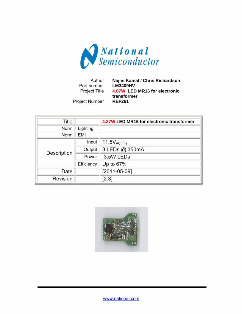
Title 4.87W LED MR16 for electronic transformer Norm Lighting
Norm EMI
Description
Input 11.5VAC.rms Output 3 LEDs @ 350mA Power 3.5W LEDs
Efficiency Up to 67%
Date [2011-05-09]
Revision [2.3]
Author Najmi Kamal / Chris Richardson Part number LM3409HV Project Title 4.87W LED MR16 for electronic
transformer Project Number REF261
4.5W LED MR16 for Electronic Transformer
National Semiconductor GmbH Livry-Gargan-Strasse 10 82256 Fürstenfeldbruck Germany
- 1-2 -
Najmi K.
2011-05-09 [Revision 2.3]
Contents
Contents .................................................................................................................... 1-2 1 Introduction ......................................................................................................... 1-3 2 Block diagram ..................................................................................................... 2-6 3 Specifications ........................................................................................................ 7 4 Basic Theory .......................................................................................................... 8
4.1 Converter Theory ............................................................................................ 8 5 Schematic ............................................................................................................ 11 6 Bill of Materials .................................................................................................... 11 7 Start up phase ..................................................................................................... 12
7.1 Plug in into the network line .......................................................................... 12 7.2 Holding time .................................................................................................. 12
8 Measurements ..................................................................................................... 13 8.1 One complete cycle: ...................................................................................... 13 8.2 Input operating waveforms ............................................................................ 14
8.2.1 Input filter ................................................................................................ 14 8.3 Main input voltage at 11.5VAC and input current with mains 230Vac. .......... 15 8.4 Power input voltage at 12VAC ........................................................................ 16
8.4.1 Switching node ....................................................................................... 17 8.4.2 Inductor current ....................................................................................... 18 8.4.3 Zoom of the drain and current inductor .................................................. 18
8.5 LED driver waveform ..................................................................................... 20 8.5.1 LED current and voltage ......................................................................... 20 8.5.2 LED current with Vin variation (min, nom and max) ............................... 21
8.6 Dimming ........................................................................................................ 23 Low dimming ........................................................................................................... 24 Zoom: ...................................................................................................................... 24
9 Protection ............................................................................................................ 25 9.1.1 Short circuit protection ............................................................................ 25 9.1.2 Open LED protection .............................................................................. 26
9.2 Efficiency ....................................................................................................... 28 9.3 Thermal behavior .......................................................................................... 29
10 Layout Design ................................................................................................... 30 11 Summary Table ................................................................................................ 31 12 Revision History ................................................................................................ 31
4.5W LED MR16 for Electronic Transformer
National Semiconductor GmbH Livry-Gargan-Strasse 10 82256 Fürstenfeldbruck Germany
- 1-3 -
Najmi K.
2011-05-09 [Revision 2.3]
1 Introduction This new LED MR16 will replace the standard halogen by driving 3 high power LEDs. This following report describes the design and shows practical test results of this LED-based MR16 designed to drive 3 LEDs in series from an AC input voltage of 11.5VAC rms generated by 50Hz magnetic transformers or Electronic transformers. Halogen MR16 bulbs do not flicker because the light emitted depends on the heat of the wire in the bulb. The heat changes more slowly compared with the change in current (50Hz) from the mains. The light emitted by LEDs changes instantly with the current. Therefore special measures need to be taken to avoid flickering. The solution is to create a system that has a power factor close to 1 to get the same behavior as the halogen bulb. Several existing approaches use a large value electrolytic capacitor after the bridge rectifier to smooth the AC waveform. This has also the advantage of keeping an output voltage higher than the forward voltage of the LEDs and provides a continuous supply voltage (Vcc) for the driver. This approach works really well with 50 Hz transformers and provides power factors of up to 0,65 .Using this method with an electronic transformer will make the LED flicker. To keep a good power factor we need to get rid of the big electrolytic capacitor after the bridge rectifier. By eliminating this capacitor, a half-sine waveform will be available going from 0V up to 12V√2. Consequently it will switch the driver on and off unless we can provide a circuit that works down to a 0V input. One of the solutions is to use a power factor correction stage and then an LED driver, but due to the board size and cost this is not the right approach. The best solution is to use a buck boost topology with the LM3409 LED driver with constant off time. With this solution, a 0.98 PF is achievable by using the IADJ pin of the IC connected via a resistor divider to the AC waveform and creating a sine-wave input current that is proportional to the input voltage. This buck boost topology provides a constant negative forward voltage for the LEDs. This forward LED voltage is applied to the IC in addition to the input voltage that supplies the driver. Therefore when the input voltage Vac reaches 0V, the minimum voltage available to the IC is three times the forward voltage of an LED. When the input voltage reaches its max peak value of 12V√2, the maximum voltage available to the driver IC is three times the forward voltage of an LED in addition to 12V√2. With this approach, we keep the driver always ON even if the input voltage reaches 0V. Phase dimming may be an option with certain combination of electronic transformer and Triac dimmer.
4.5W LED MR16 for Electronic Transformer
National Semiconductor GmbH Livry-Gargan-Strasse 10 82256 Fürstenfeldbruck Germany
- 1-4 -
Najmi K.
2011-05-09 [Revision 2.3]
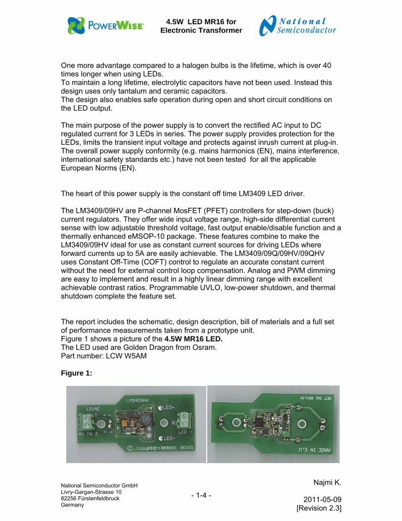
One more advantage compared to a halogen bulbs is the lifetime, which is over 40 times longer when using LEDs. To maintain a long lifetime, electrolytic capacitors have not been used. Instead this design uses only tantalum and ceramic capacitors. The design also enables safe operation during open and short circuit conditions on the LED output. The main purpose of the power supply is to convert the rectified AC input to DC regulated current for 3 LEDs in series. The power supply provides protection for the LEDs, limits the transient input voltage and protects against inrush current at plug-in. The overall power supply conformity (e.g. mains harmonics (EN), mains interference, international safety standards etc.) have not been tested for all the applicable European Norms (EN). The heart of this power supply is the constant off time LM3409 LED driver. The LM3409/09HV are P-channel MosFET (PFET) controllers for step-down (buck) current regulators. They offer wide input voltage range, high-side differential current sense with low adjustable threshold voltage, fast output enable/disable function and a thermally enhanced eMSOP-10 package. These features combine to make the LM3409/09HV ideal for use as constant current sources for driving LEDs where forward currents up to 5A are easily achievable. The LM3409/09Q/09HV/09QHV uses Constant Off-Time (COFT) control to regulate an accurate constant current without the need for external control loop compensation. Analog and PWM dimming are easy to implement and result in a highly linear dimming range with excellent achievable contrast ratios. Programmable UVLO, low-power shutdown, and thermal shutdown complete the feature set. The report includes the schematic, design description, bill of materials and a full set of performance measurements taken from a prototype unit. Figure 1 shows a picture of the 4.5W MR16 LED. The LED used are Golden Dragon from Osram. Part number: LCW W5AM Figure 1:
4.5W LED MR16 for Electronic Transformer
National Semiconductor GmbH Livry-Gargan-Strasse 10 82256 Fürstenfeldbruck Germany
- 1-5 -
Najmi K.
2011-05-09 [Revision 2.3]
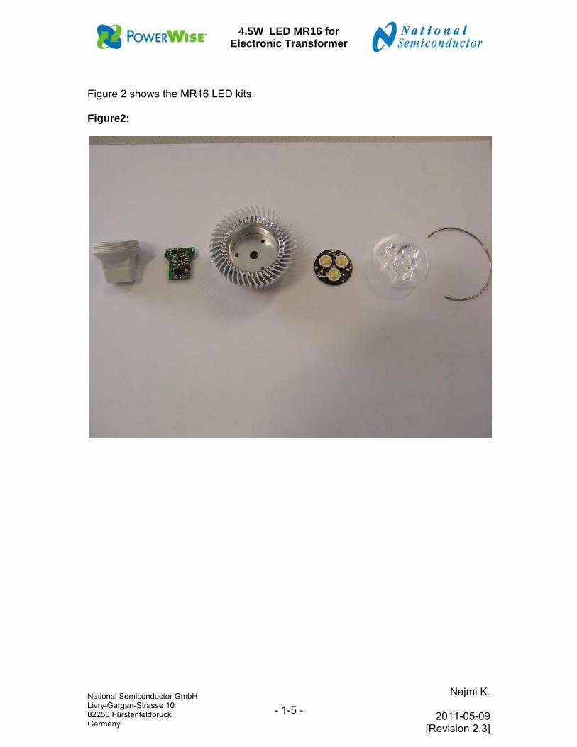
Figure 2 shows the MR16 LED kits. Figure2:

4.5W LED MR16 for Electronic Transformer
National Semiconductor GmbH Livry-Gargan-Strasse 10 82256 Fürstenfeldbruck Germany
- 2-6 -
Najmi K.
2011-05-09 [Revision 2.3]
2 Block diagram

4.5W LED MR16 for Electronic Transformer
National Semiconductor GmbH Livry-Gargan-Strasse 10 82256 Fürstenfeldbruck Germany
- 7 -
Najmi K.
2011-05-09 [Revision 2.3]
3 Specifications Specification Model REF 261 Max input power (W) 4.87W DC Output current 350mA # of LEDs
LEDs 3 Osram
Input Voltage (AC) 0VAC …..14 VAC PF 0.94 Efficiency (%) 67% Output Voltage (depending on LED VF ) 8.8V +/-20% Current (A) 0.350A Ripple (mApp) 500mA with 350mA
LED current Frequency ripple 100hz Start up time (ms) Hold up time (input failure) Remote sensing Remote on/off Yes, ON/OFF switch Isolation Input/output No
Dimming With TRIAC Dimmer* Yes* Standards Safety Agency approvals
IEC 61000-3-2 CLASS C No No
EN55015 conduction EN55015 radiation
No No
Other Cooling method passive Life time (NO ELCO) Temperature range -20°C to +…..°C Maximum component height is 8 mm. The overall size area is 20mm by 18mm. *Combination of certain Triac and certain Electronic transformer for dimming.

4.5W LED MR16 for Electronic Transformer
National Semiconductor GmbH Livry-Gargan-Strasse 10 82256 Fürstenfeldbruck Germany
- 8 -
Najmi K.
2011-05-09 [Revision 2.3]
4 Basic Theory
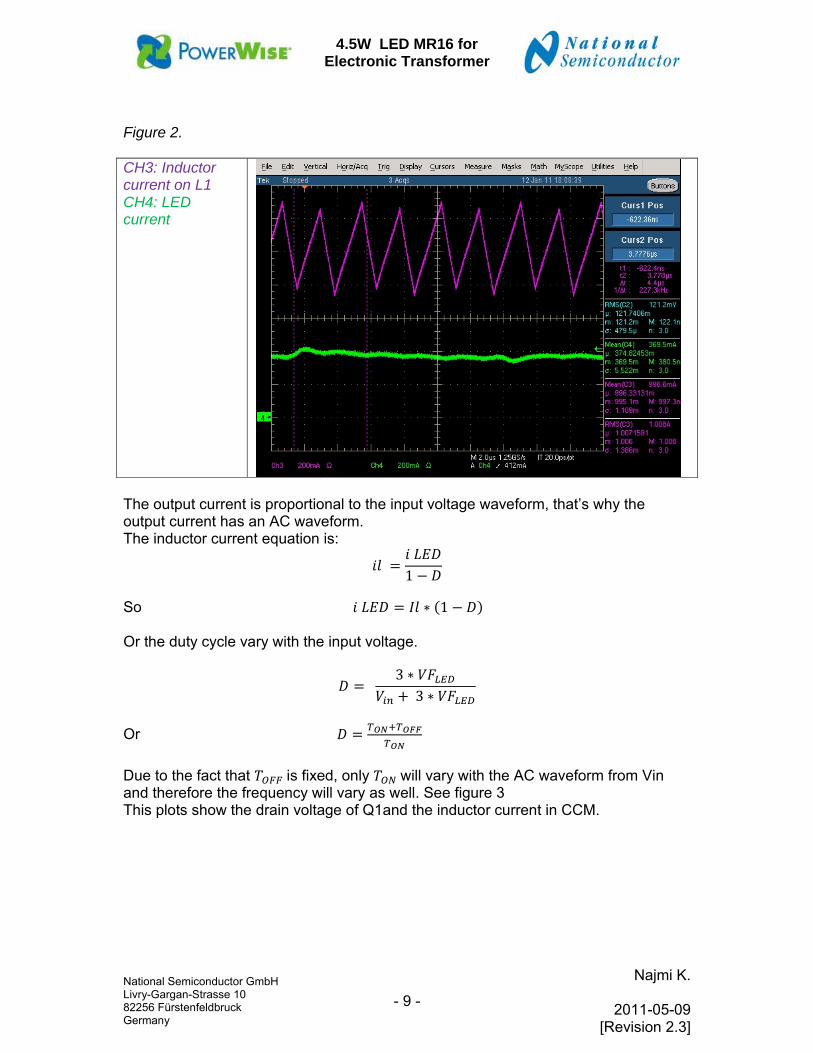
4.1 Converter Theory During the time that the PFET (Q1) is turned on (tON), the input voltage charges up the inductor (L1) until reaching the peak current fixed by R8. while the output capacitor (CO) provides energy to the LED .Then Q1 is turned off during a certain time fixed by R5, C4 and forward voltage of the LEDs, the re-circulating diode (D1) becomes forward biased and L1 discharges the energy on the output cap C7 and on the LEDs. During the Ton time the LED current is supplied by the C7. During Toff time the LED current Figure 1 shows the inductor current on one AC cycle and LED current. Figure 2 is a zoom of the inductor current on one AC cycle and LED current. Figure 1. CH3: Inductor current on L1 CH4: LED current
4.5W LED MR16 for Electronic Transformer
National Semiconductor GmbH Livry-Gargan-Strasse 10 82256 Fürstenfeldbruck Germany
- 9 -
Najmi K.
2011-05-09 [Revision 2.3]
Figure 2. CH3: Inductor current on L1 CH4: LED current
The output current is proportional to the input voltage waveform, that’s why the output current has an AC waveform. The inductor current equation is:
1
So 1 Or the duty cycle vary with the input voltage.
3
3
Or
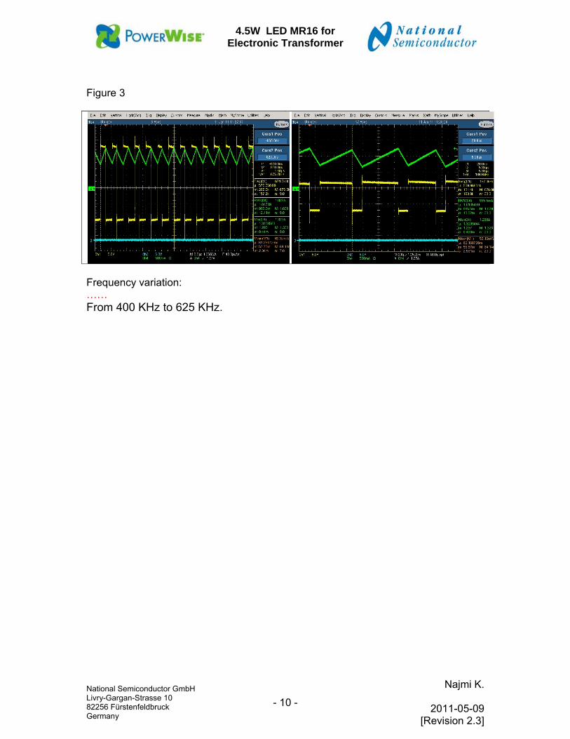
Due to the fact that is fixed, only will vary with the AC waveform from Vin and therefore the frequency will vary as well. See figure 3 This plots show the drain voltage of Q1and the inductor current in CCM.
4.5W LED MR16 for Electronic Transformer
National Semiconductor GmbH Livry-Gargan-Strasse 10 82256 Fürstenfeldbruck Germany
- 10 -
Najmi K.
2011-05-09 [Revision 2.3]
Figure 3
Frequency variation: …… From 400 KHz to 625 KHz.
4.5W LED MR16 for Electronic Transformer
National Semiconductor GmbH Livry-Gargan-Strasse 10 82256 Fürstenfeldbruck Germany
- 11 -
Najmi K.
2011-05-09 [Revision 2.3]
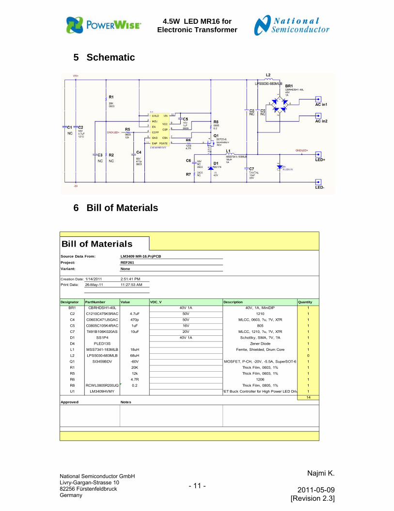
5 Schematic
6 Bill of Materials
Bill of MaterialsSource Data From: LM3409 MR-16.PrjPCB
Project: REF261
Variant: None
Creation Date: 1/14/2011 2:51:41 PM
Print Date: 26-May-11 11:27:53 AM
Designator PartNumber Value VDC_V Description Quantity
BR1 CBRHDSH1-40L 40V 1A 40V, 1A, MiniDIP 1
C2 C1210C475K5RAC 4.7uF 50V 1210 1
C4 C0603C471J5GAC 470p 50V MLCC, 0603, ?u, ?V, X7R 1
C5 C0805C105K4RAC 1uF 16V 805 1
C7 T491B106K020AS 10uF 20V MLCC, 1210, ?u, ?V, X7R 1
D1 SS1P4 40V 1A Schottky, SMA, ?V, ?A 1
D4 PLED13S Zener Diode 1
L1 MSS7341-183MLB 18uH Ferrite, Shielded, Drum Core 1
L2 LPS5030-683MLB 68uH 0
Q1 SI3459BDV -60V MOSFET, P-CH, -20V, -5.5A, SuperSOT-6 1
R1 20K Thick Film, 0603, 1% 1
R5 12k Thick Film, 0603, 1% 1
R6 4.7R 1206 1
R8 RCWL0805R200JQ 0.2 Thick Film, 0805, 1% 1
U1 LM3409HVMY FET Buck Controller for High Power LED Driv 1
14Approved Notes

4.5W LED MR16 for Electronic Transformer
National Semiconductor GmbH Livry-Gargan-Strasse 10 82256 Fürstenfeldbruck Germany
- 12 -
Najmi K.
2011-05-09 [Revision 2.3]
7 Start up phase
7.1 Plug in into the network line CH2: input Voltage CH3: Inductor current CH4: LED current Condition : Measurement done at hot plug. Vin main: 230VAC Output: [email protected]
7.2 Holding time CH2: input Voltage CH3: Inductor current CH4: LED current Condition : Measurement done at plug out Vin: 230VAC Vout: 3 LEDs @0.35A Holding time: 0 ms
4.5W LED MR16 for Electronic Transformer
National Semiconductor GmbH Livry-Gargan-Strasse 10 82256 Fürstenfeldbruck Germany
- 13 -
Najmi K.
2011-05-09 [Revision 2.3]
8 Measurements
8.1 One complete cycle: This plot shows in detail the drain source voltage and drain current of Q1 for one complete cycle at full power on the LED driver. The cycle can be divided into different phases as shown on the plot: 1. Switch on phase 2. Conducting phase 3. Switch off phase 4. Off phase, Energy released into the load
1
4.5W LED MR16 for Electronic Transformer
National Semiconductor GmbH Livry-Gargan-Strasse 10 82256 Fürstenfeldbruck Germany
- 14 -
Najmi K.
2011-05-09 [Revision 2.3]
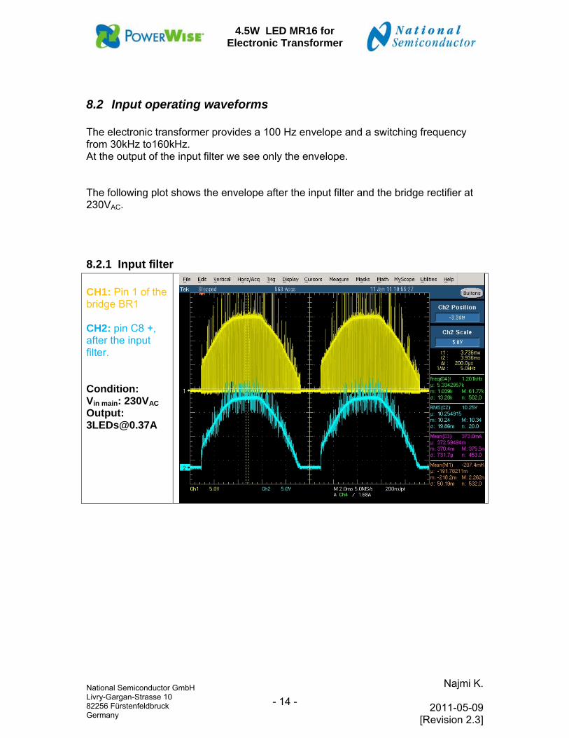
8.2 Input operating waveforms The electronic transformer provides a 100 Hz envelope and a switching frequency from 30kHz to160kHz. At the output of the input filter we see only the envelope. The following plot shows the envelope after the input filter and the bridge rectifier at 230VAC.
8.2.1 Input filter CH1: Pin 1 of the bridge BR1 CH2: pin C8 +, after the input filter. Condition: Vin main: 230VAC Output: [email protected]
4.5W LED MR16 for Electronic Transformer
National Semiconductor GmbH Livry-Gargan-Strasse 10 82256 Fürstenfeldbruck Germany
- 15 -
Najmi K.
2011-05-09 [Revision 2.3]
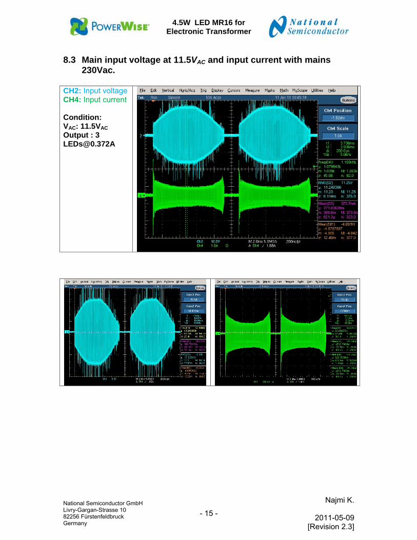
8.3 Main input voltage at 11.5VAC and input current with mains 230Vac.
CH2: Input voltage CH4: Input current Condition: VAC: 11.5VAC Output : 3 [email protected]

4.5W LED MR16 for Electronic Transformer
National Semiconductor GmbH Livry-Gargan-Strasse 10 82256 Fürstenfeldbruck Germany
- 16 -
Najmi K.
2011-05-09 [Revision 2.3]
8.4 Power input voltage at 12VAC Input power: 4.88W for 373mA current LED CH2: Input voltage CH4: Input current M1: Power input Condition: Vin main: 230VAC Output : 3 [email protected]
ZOOM: CH2: Input voltage CH4: Input current M1: Power input Condition: Vin main: 230VAC Output : 3 [email protected]
4.5W LED MR16 for Electronic Transformer
National Semiconductor GmbH Livry-Gargan-Strasse 10 82256 Fürstenfeldbruck Germany
- 17 -
Najmi K.
2011-05-09 [Revision 2.3]
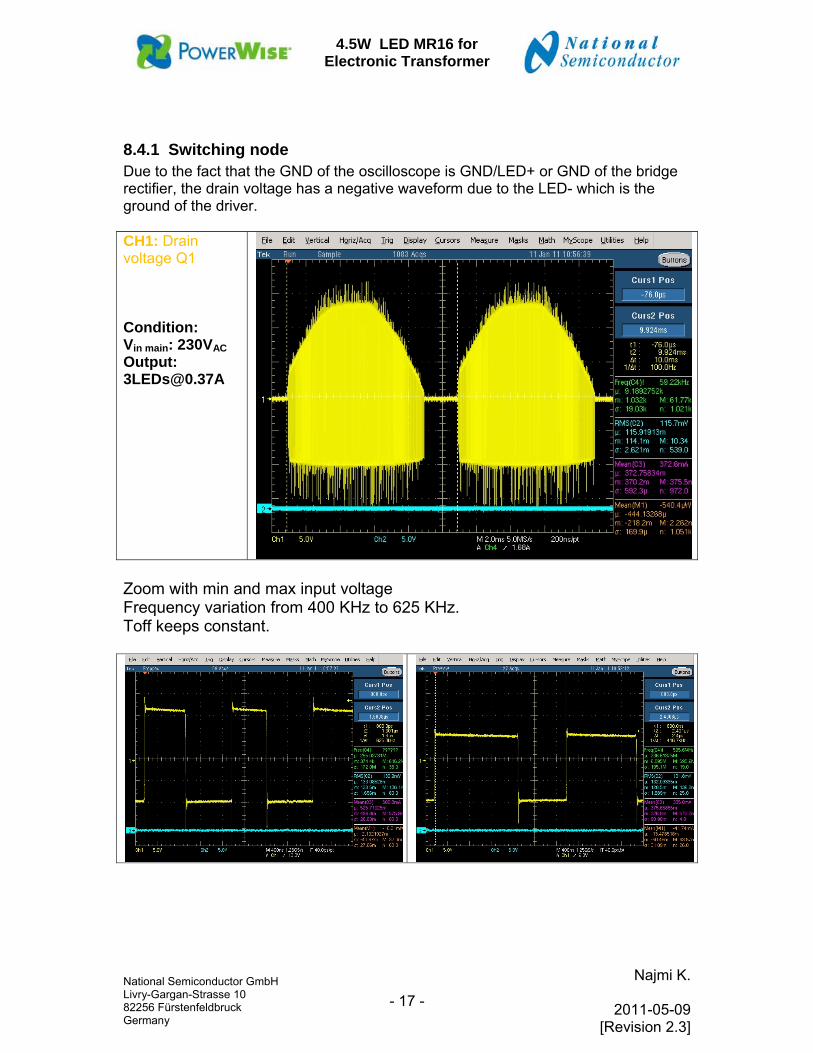
8.4.1 Switching node Due to the fact that the GND of the oscilloscope is GND/LED+ or GND of the bridge rectifier, the drain voltage has a negative waveform due to the LED- which is the ground of the driver. CH1: Drain voltage Q1 Condition: Vin main: 230VAC Output: [email protected]
Zoom with min and max input voltage Frequency variation from 400 KHz to 625 KHz. Toff keeps constant.

4.5W LED MR16 for Electronic Transformer
National Semiconductor GmbH Livry-Gargan-Strasse 10 82256 Fürstenfeldbruck Germany
- 18 -
Najmi K.
2011-05-09 [Revision 2.3]
8.4.2 Inductor current The inductor current is constant because we regulate on the peak current of the inductor. CH1: Drain voltage Q1 CH4: Inductor current Condition: Vin main: 230VAC Output: [email protected]
8.4.3 Zoom of the drain and current inductor The following plot shows the drain voltage and the inductor current at min and max input voltage after the electronic transformer. CH1: Drain voltage Q1 CH4: Inductor current Condition: Vin main: 230VAC Vin : 12Vmax Output: [email protected]

4.5W LED MR16 for Electronic Transformer
National Semiconductor GmbH Livry-Gargan-Strasse 10 82256 Fürstenfeldbruck Germany
- 19 -
Najmi K.
2011-05-09 [Revision 2.3]
CH1: Drain voltage Q1 CH4: Inductor current Condition: Vin main: 230VAC
Vin : 2Vmin low Vin Output: [email protected]
4.5W LED MR16 for Electronic Transformer
National Semiconductor GmbH Livry-Gargan-Strasse 10 82256 Fürstenfeldbruck Germany
- 20 -
Najmi K.
2011-05-09 [Revision 2.3]
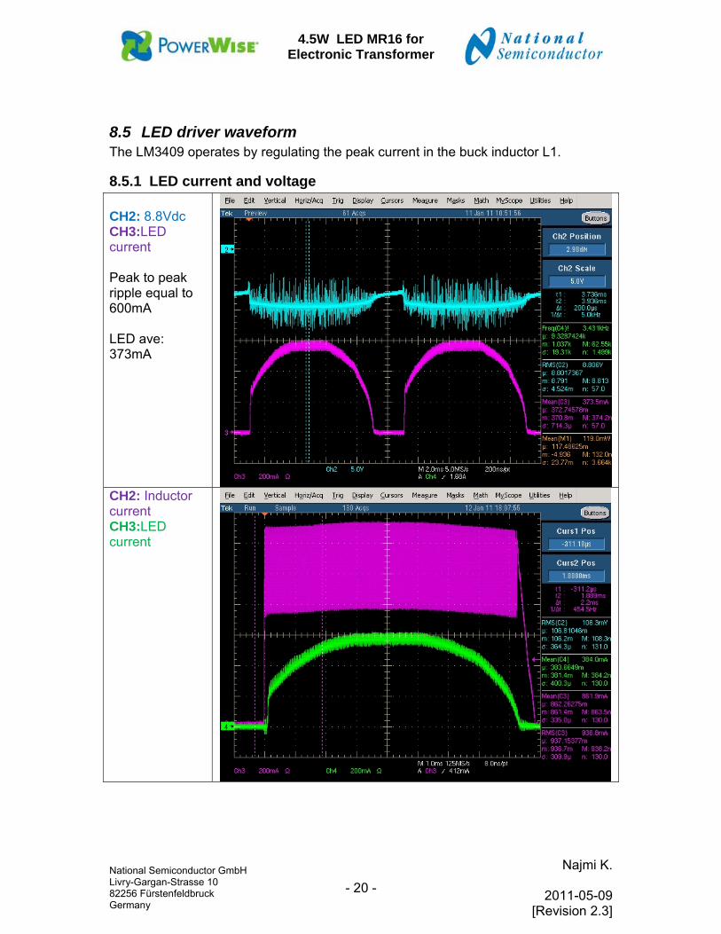
8.5 LED driver waveform The LM3409 operates by regulating the peak current in the buck inductor L1.
8.5.1 LED current and voltage CH2: 8.8Vdc CH3:LED current Peak to peak ripple equal to 600mA LED ave: 373mA
CH2: Inductor current CH3:LED current
4.5W LED MR16 for Electronic Transformer
National Semiconductor GmbH Livry-Gargan-Strasse 10 82256 Fürstenfeldbruck Germany
- 21 -
Najmi K.
2011-05-09 [Revision 2.3]
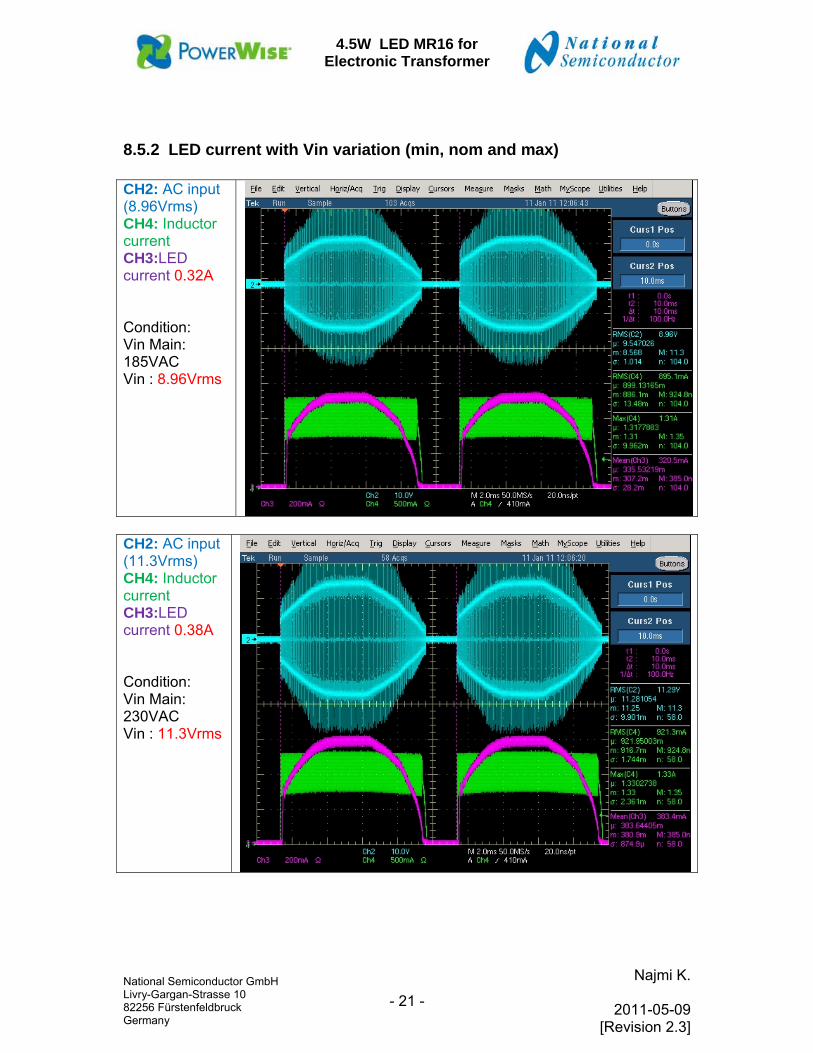
8.5.2 LED current with Vin variation (min, nom and max) CH2: AC input (8.96Vrms) CH4: Inductor current CH3:LED current 0.32A Condition: Vin Main: 185VAC Vin : 8.96Vrms
CH2: AC input (11.3Vrms) CH4: Inductor current CH3:LED current 0.38A Condition: Vin Main: 230VAC Vin : 11.3Vrms

4.5W LED MR16 for Electronic Transformer
National Semiconductor GmbH Livry-Gargan-Strasse 10 82256 Fürstenfeldbruck Germany
- 22 -
Najmi K.
2011-05-09 [Revision 2.3]
CH2: AC input (12Vrms) CH4: Inductor current CH3:LED current 0.40A Condition: Vin Main: 245VAC Vin : 12Vrms
4.5W LED MR16 for Electronic Transformer
National Semiconductor GmbH Livry-Gargan-Strasse 10 82256 Fürstenfeldbruck Germany
- 23 -
Najmi K.
2011-05-09 [Revision 2.3]
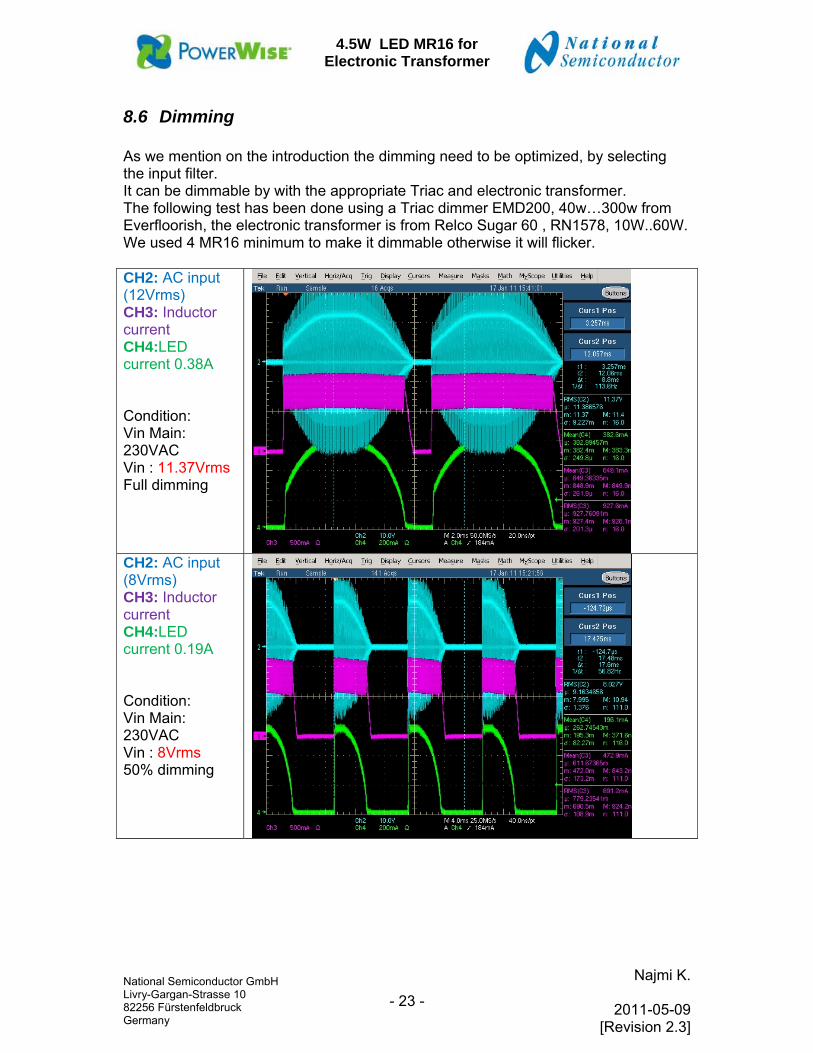
8.6 Dimming As we mention on the introduction the dimming need to be optimized, by selecting the input filter. It can be dimmable by with the appropriate Triac and electronic transformer. The following test has been done using a Triac dimmer EMD200, 40w…300w from Everfloorish, the electronic transformer is from Relco Sugar 60 , RN1578, 10W..60W. We used 4 MR16 minimum to make it dimmable otherwise it will flicker. CH2: AC input (12Vrms) CH3: Inductor current CH4:LED current 0.38A Condition: Vin Main: 230VAC Vin : 11.37Vrms Full dimming
CH2: AC input (8Vrms) CH3: Inductor current CH4:LED current 0.19A Condition: Vin Main: 230VAC Vin : 8Vrms 50% dimming

4.5W LED MR16 for Electronic Transformer
National Semiconductor GmbH Livry-Gargan-Strasse 10 82256 Fürstenfeldbruck Germany
- 24 -
Najmi K.
2011-05-09 [Revision 2.3]
CH2: AC input (2.47Vrms) CH3: Inductor current CH4:LED current 0.032A Condition: Vin Main: 230VAC Vin : 2.47Vrms
Low dimming
Zoom: CH2: AC input (2.47Vrms) CH3: Inductor current CH4:LED current 0.032A Condition: Vin Main: 230VAC Vin : 2.47Vrms Low dimming

4.5W LED MR16 for Electronic Transformer
National Semiconductor GmbH Livry-Gargan-Strasse 10 82256 Fürstenfeldbruck Germany
- 25 -
Najmi K.
2011-05-09 [Revision 2.3]
9 Protection For safety reasons and to fulfill short circuit requirements, it has been ensured that no component should overheat and burn in case of short circuit. The short circuit test has been done before and after plug in.
9.1.1 Short circuit protection The cycle by cycle current limiting controls the maximum power in case of short circuit or an excessive load. The following plots show a typical protection after short circuit on the LEDs. CH1: drain voltage Q1 CH3: LED current CH4: Inductor current Condition: SHORT CIRCUIT No TRIAC dimmer Vin main:230VAC
As soon as the short circuit is removed from the output, the power supply will go back to the regulated current 350mA.
4.5W LED MR16 for Electronic Transformer
National Semiconductor GmbH Livry-Gargan-Strasse 10 82256 Fürstenfeldbruck Germany
- 26 -
Najmi K.
2011-05-09 [Revision 2.3]
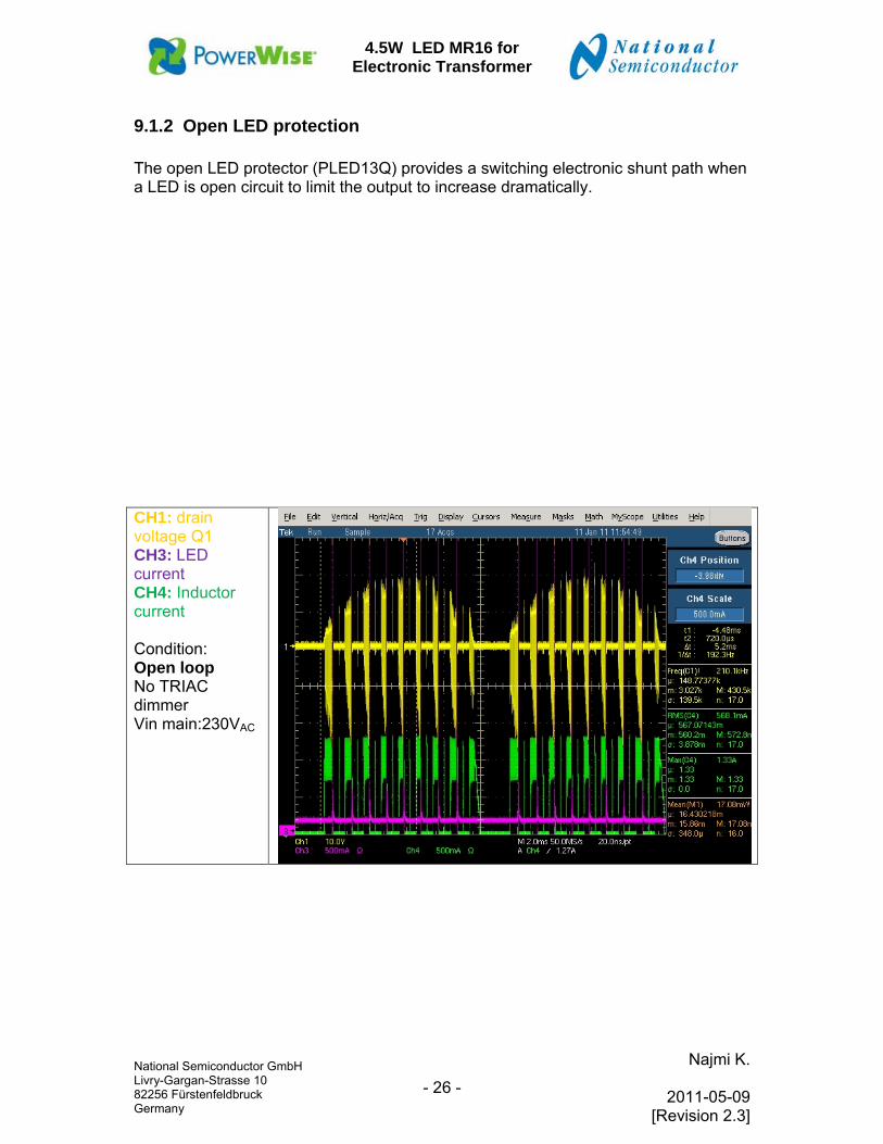
9.1.2 Open LED protection The open LED protector (PLED13Q) provides a switching electronic shunt path when a LED is open circuit to limit the output to increase dramatically.
CH1: drain voltage Q1 CH3: LED current CH4: Inductor current Condition: Open loop No TRIAC dimmer Vin main:230VAC

4.5W LED MR16 for Electronic Transformer
National Semiconductor GmbH Livry-Gargan-Strasse 10 82256 Fürstenfeldbruck Germany
- 27 -
Najmi K.
2011-05-09 [Revision 2.3]
CH1: Output voltage on the LED string CH3: LED current CH4: Inductor current Condition: Open loop No TRIAC dimmer Vin main:230VAC

4.5W LED MR16 for Electronic Transformer
National Semiconductor GmbH Livry-Gargan-Strasse 10 82256 Fürstenfeldbruck Germany
- 28 -
Najmi K.
2011-05-09 [Revision 2.3]
9.2 Efficiency Due to the fact that we use a buck boost topology, a rectified bridge for high switching frequency an input filter and a small form factor, we can assume a low efficiency. The efficiency may differ from electronic transformer. The input power measured is 4.87W at 230VAC main. The output power is 3.27W into the LEDs. 8.8V * 372ma =3.27W EFF: 0.67%
4.5W LED MR16 for Electronic Transformer
National Semiconductor GmbH Livry-Gargan-Strasse 10 82256 Fürstenfeldbruck Germany
- 29 -
Najmi K.
2011-05-09 [Revision 2.3]
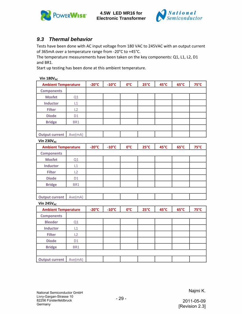
9.3 Thermal behavior Tests have been done with AC input voltage from 180 VAC to 245VAC with an output current of 365mA over a temperature range from ‐20°C to +45°C. The temperature measurements have been taken on the key components: Q1, L1, L2, D1 and BR1. Start up testing has been done at this ambient temperature. Vin 180VAC
Ambient Temperature ‐20°C ‐10°C 0°C 25°C 45°C 65°C 75°C
Components
Mosfet Q1
Inductor L1
Filter L2
Diode D1
Bridge BR1
Output current Ave(mA)
Vin 230VAC
Ambient Temperature ‐20°C ‐10°C 0°C 25°C 45°C 65°C 75°C
Components
Mosfet Q1
Inductor L1
Filter L2
Diode D1
Bridge BR1
Output current Ave(mA)
Vin 245VAC
Ambient Temperature ‐20°C ‐10°C 0°C 25°C 45°C 65°C 75°C
Components
Bleeder Q1
Inductor L1
Filter L2
Diode D1
Bridge BR1
Output current Ave(mA)
4.5W LED MR16 for Electronic Transformer
National Semiconductor GmbH Livry-Gargan-Strasse 10 82256 Fürstenfeldbruck Germany
- 30 -
Najmi K.
2011-05-09 [Revision 2.3]
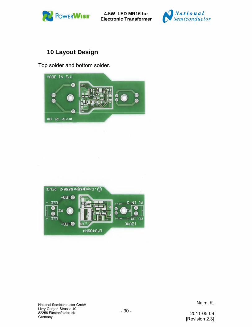
10 Layout Design Top solder and bottom solder.
4.5W LED MR16 for Electronic Transformer
National Semiconductor GmbH Livry-Gargan-Strasse 10 82256 Fürstenfeldbruck Germany
- 31 -
Najmi K.
2011-05-09 [Revision 2.3]
11 Summary Table Several investigations need to be done on the input filter to make it run with dimming using different Triac dimmer.
12 Revision History
Status Date Description of change (s) rev02 28/01/2011 L2 = LPS5030-683MLB
Polarity on D4 changed on schematic Rev2.1 07/02/2011 Add Frequency ripple 100hz on specification Rev 2.2 09/05/2011 Flickers and start up problem solved
Bom update. Rev2.3 25/05/2011 High peak input current solved by L2.

IMPORTANT NOTICE
Texas Instruments Incorporated and its subsidiaries (TI) reserve the right to make corrections, modifications, enhancements, improvements,and other changes to its products and services at any time and to discontinue any product or service without notice. Customers shouldobtain the latest relevant information before placing orders and should verify that such information is current and complete. All products aresold subject to TI’s terms and conditions of sale supplied at the time of order acknowledgment.
TI warrants performance of its hardware products to the specifications applicable at the time of sale in accordance with TI’s standardwarranty. Testing and other quality control techniques are used to the extent TI deems necessary to support this warranty. Except wheremandated by government requirements, testing of all parameters of each product is not necessarily performed.
TI assumes no liability for applications assistance or customer product design. Customers are responsible for their products andapplications using TI components. To minimize the risks associated with customer products and applications, customers should provideadequate design and operating safeguards.
TI does not warrant or represent that any license, either express or implied, is granted under any TI patent right, copyright, mask work right,or other TI intellectual property right relating to any combination, machine, or process in which TI products or services are used. Informationpublished by TI regarding third-party products or services does not constitute a license from TI to use such products or services or awarranty or endorsement thereof. Use of such information may require a license from a third party under the patents or other intellectualproperty of the third party, or a license from TI under the patents or other intellectual property of TI.
Reproduction of TI information in TI data books or data sheets is permissible only if reproduction is without alteration and is accompaniedby all associated warranties, conditions, limitations, and notices. Reproduction of this information with alteration is an unfair and deceptivebusiness practice. TI is not responsible or liable for such altered documentation. Information of third parties may be subject to additionalrestrictions.
Resale of TI products or services with statements different from or beyond the parameters stated by TI for that product or service voids allexpress and any implied warranties for the associated TI product or service and is an unfair and deceptive business practice. TI is notresponsible or liable for any such statements.
TI products are not authorized for use in safety-critical applications (such as life support) where a failure of the TI product would reasonablybe expected to cause severe personal injury or death, unless officers of the parties have executed an agreement specifically governingsuch use. Buyers represent that they have all necessary expertise in the safety and regulatory ramifications of their applications, andacknowledge and agree that they are solely responsible for all legal, regulatory and safety-related requirements concerning their productsand any use of TI products in such safety-critical applications, notwithstanding any applications-related information or support that may beprovided by TI. Further, Buyers must fully indemnify TI and its representatives against any damages arising out of the use of TI products insuch safety-critical applications.
TI products are neither designed nor intended for use in military/aerospace applications or environments unless the TI products arespecifically designated by TI as military-grade or "enhanced plastic." Only products designated by TI as military-grade meet militaryspecifications. Buyers acknowledge and agree that any such use of TI products which TI has not designated as military-grade is solely atthe Buyer's risk, and that they are solely responsible for compliance with all legal and regulatory requirements in connection with such use.
TI products are neither designed nor intended for use in automotive applications or environments unless the specific TI products aredesignated by TI as compliant with ISO/TS 16949 requirements. Buyers acknowledge and agree that, if they use any non-designatedproducts in automotive applications, TI will not be responsible for any failure to meet such requirements.
Following are URLs where you can obtain information on other Texas Instruments products and application solutions:
Products Applications
Audio www.ti.com/audio Automotive and Transportation www.ti.com/automotive
Amplifiers amplifier.ti.com Communications and Telecom www.ti.com/communications
Data Converters dataconverter.ti.com Computers and Peripherals www.ti.com/computers
DLP® Products www.dlp.com Consumer Electronics www.ti.com/consumer-apps
DSP dsp.ti.com Energy and Lighting www.ti.com/energy
Clocks and Timers www.ti.com/clocks Industrial www.ti.com/industrial
Interface interface.ti.com Medical www.ti.com/medical
Logic logic.ti.com Security www.ti.com/security
Power Mgmt power.ti.com Space, Avionics and Defense www.ti.com/space-avionics-defense
Microcontrollers microcontroller.ti.com Video and Imaging www.ti.com/video
RFID www.ti-rfid.com
OMAP Mobile Processors www.ti.com/omap
Wireless Connectivity www.ti.com/wirelessconnectivity
TI E2E Community Home Page e2e.ti.com
Mailing Address: Texas Instruments, Post Office Box 655303, Dallas, Texas 75265Copyright © 2012, Texas Instruments Incorporated


![Transformer Compatibility _EU LED Lamps _MR16 MR16 _7.0W : SAMSUNG Electronics LED MR16 Transformer compatibility list [Non-dimmable] MR16 _3.2W MR16 _5.0W](https://img.dokumen.tips/doc/110x75/5519e6c15503467a178b4965/transformer-compatibility-eu-led-lamps-mr16-mr16-70w-samsung-electronics-led-mr16-transformer-compatibility-list-non-dimmable-mr16-32w-mr16-50w.jpg)