Embed Size (px)
Citation preview

1
GSM
6332
www.gs-power.com
N & P Pair Enhancement Mode MOSFET
Product Description Features N-Channel
20V/1.0A,RDS(ON)=280mΩ@VGS=4.5V 20V/0.8A,RDS(ON)=340mΩ@VGS=2.5V 20V/0.7A,RDS(ON)=580mΩ@VGS=1.8V
P-Channel -20V/-1.0A,RDS(ON)= 600mΩ@VGS=-4.5V -20V/-0.8A,RDS(ON)= 800mΩ@VGS=-2.5V -20V/-0.7A,RDS(ON)= 1440mΩ@VGS=-1.8V
Low-Voltage Operation High-Speed Circuits Low Battery Voltage Operation SOT-363 package design
Applications
The GSM6332 is the N and P Pair enhancement mode MOSFET, uses Advanced Trench Technology to provide excellent RDS(ON) , low gate charge. These devices are particularly suited for low voltage power management, such as smart phone and notebook computer and other battery powered circuits, and low in-line power loss are needed in commercial industrial surface mount applications.
Load Switch for Portable Devices, Smart Phones, Pagers.
Packages & Pin Assignments
GSM6332X6F(SOT-363/SC-70-6L)
1 Source 1 2 Gate 1 3 Drain 2 4 Source 2 5 Gate 2 6 Drain 1

2 www.gs-power.com
GSM
6332
Ordering Information
Marking Information
Absolute Maximum Ratings TA=25ºC unless otherwise noted
Typical Symbol Parameter N-Channel P-Channel
Unit
VDSS Drain-Source Voltage 20 -20 V
VGSS Gate-Source Voltage ±12 ±12 V
TA =25ºC 1.0 -1.0 ID Continuous Drain Current(TJ=150ºC)
TA =70ºC 0.7 -0.7 A
IDM Pulsed Drain Current 6 -6 A
IS Continuous Source Current(Diode Conduction) 1 -1 A
TA =25ºC 0.3 PD Power Dissipation
TA =70ºC 0.2 W
TJ Operating Junction Temperature -55/150 ºC
TSTG Storage Temperature Range -55/150 ºC
Part Number Package Part Marking
GSM6332X6F SOT-363 32YW

3 www.gs-power.com
GSM
6332
Electrical Characteristics TA=25ºC unless otherwise noted
Symbol Parameter Conditions Min Typ Max UnitStatic
VGS=0V,ID=250uA N-Ch 20 V(BR)DSS Drain-Source Breakdown
Voltage VGS=0V,ID=-250uA P-Ch -20
VDS=VGS,ID=250uA N-Ch 0.4 1.0 VGS(th) Gate Threshold Voltage
VDS=VGS,ID=-250uA P-Ch -0.4 -1.0
V
VDS=0V,VGS=±12V N-Ch ±100 IGSS Gate Leakage Current
VDS=0V,VGS=±12V P-Ch ±100 nA
VDS=20V,VGS=0V N-Ch 1
VDS=-20V,VGS=0V P-Ch -1
VDS=20V,VGS=0V TJ=85ºC N-Ch 5 IDSS Zero Gate Voltage Drain
Current
VDS=-20V,VGS=0V TJ=85ºC P-Ch -5
uA
VDS≥5V,VGS=4.5V N-Ch 1.2 ID(on) On-State Drain Current
VDS≤-5V,VGS=4.5V P-Ch 0.7 A
VGS=4.5V,ID=1.0A N-Ch 280
VGS=-4.5V,ID=-1.0A P-Ch 600
VGS=2.5V,ID=0.8A N-Ch 340
VGS=-2.5V,ID=-0.8A P-Ch 800
VGS=1.8V,ID=0.7A N-Ch 580
RDS(on) Drain-Source On-Resistance
VGS=-1.8V,ID=-0.7A P-Ch 1440
mΩ
VDS=10V,ID=1.0A N-Ch 1 gfs Forward Transconductance
VDS=-10V,ID=-0.4A P-Ch 1 S
IS=1.0A,VGS=0V N-Ch 0.65 1.2 VSD Diode Forward Voltage
IS=-0.15A,VGS=0V P-Ch -0.65 -1.2 V
Dynamic
VDS=10V,VGS=0V, f=1MHz N-Ch 70
Ciss Input Capacitance VDS=-10V,VGS=0V,
f=1MHz P-Ch 70
VDS=10V,VGS=0V, f=1MHz N-Ch 20
Coss Output Capacitance VDS=-10V,VGS=0V,
f=1MHz P-Ch 20
VDS=10V,VGS=0V, f=1MHz N-Ch 8
Crss Reverse Transfer Capacitance VDS=-10V,VGS=0V,
f=1MHz P-Ch 10
pF
N-Ch 1.06 1.38 Qg Total Gate Charge
P-Ch 1.0 1.3
N-Ch 0.18 Qgs Gate-Source Charge
P-Ch 0.1
N-Ch 0.32 Qgd Gate-Drain Charge
N-Channel VDS=10V,VGS=4.5V,ID=1.2A
P-Channel
VDS=-10V,VGS=-4.5V , ID=-0.25A
P-Ch 0.3
nC
4 www.gs-power.com
GSM
6332
Electrical Characteristics (Continue) TA=25ºC unless otherwise noted
N-Ch 18 26 td(on) P-Ch 10 15
N-Ch 20 28 tr
Turn-On Time
P-Ch 10 15
N-Ch 70 110 td(off)
P-Ch 40 60
N-Ch 25 40 tf
Turn-Off Time
N-Channel VDD=10V,RL=20Ω,ID=1.2A
VGEN=4.5V,RG=1Ω
P-Channel VDD=-10V,RL=30Ω,ID=-0.2A
VGEN=-4.5V,RG=10Ω
P-Ch 30 50
ns
Typical Performance Characteristics (N-Channel)

5 www.gs-power.com
GSM
6332
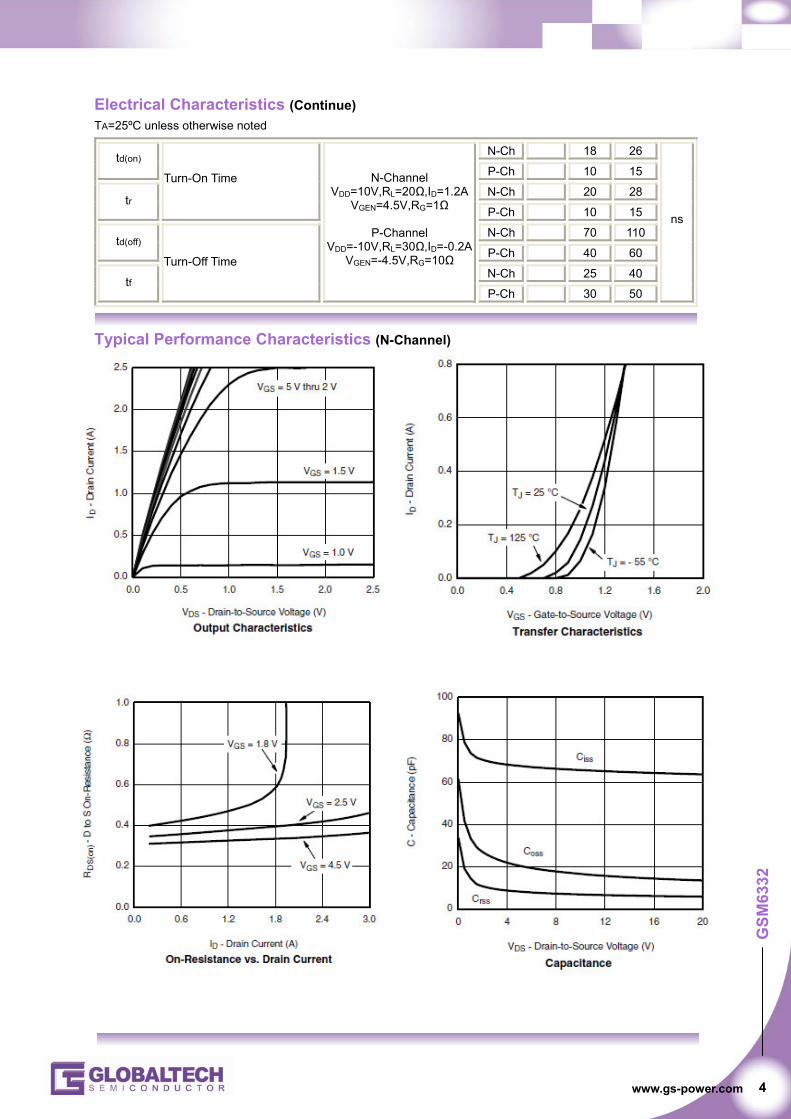
Typical Performance Characteristics (N-Channel)

6 www.gs-power.com
GSM
6332
Typical Performance Characteristics (N-Channel)
7 www.gs-power.com
GSM
6332
Typical Performance Characteristics (N-Channel)

8 www.gs-power.com
GSM
6332
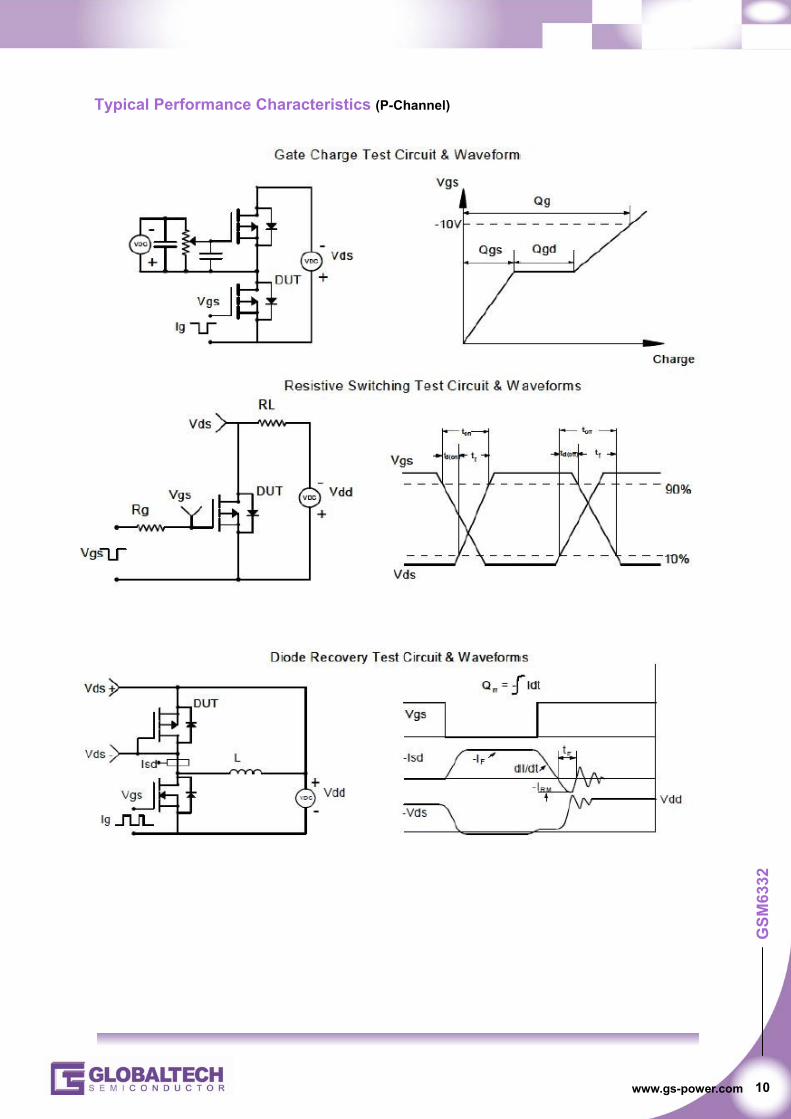
Typical Performance Characteristics (P-Channel)

9 www.gs-power.com
GSM
6332
Typical Performance Characteristics (P-Channel)
10www.gs-power.com
GSM
6332
Typical Performance Characteristics (P-Channel)

11www.gs-power.com
GSM
6332
Package Dimension
SOT-363
Dimensions Millimeters Inches
Symbol Min Max Min Max
A 0.900 1.100 0.035 0.043
A1 0.000 0.100 0.000 0.004
A2 0.900 1.000 0.035 0.039
b 0.150 0.350 0.006 0.014
c 0.080 0.150 0.003 0.006
D 2.000 2.200 0.079 0.087
E 1.150 1.350 0.045 0.053
E1 2.150 2.450 0.085 0.096
e 0.650 (TYP) 0.026 (TYP)
e1 1.200 1.400 0.047 0.055
L 0.525 (REF) 0.021 (REF)
L1 0.260 0.460 0.010 0.018
θ 0º 8 º 0º 8 º

NoticeVersion_1.3
NOTICE
Information furnished is believed to be accurate and reliable. However Globaltech Semiconductor assumes no responsibility for the consequences of use of such information nor for any infringement of patents or other rights of third parties, which may result from its use. No license is granted by implication or otherwise under any patent or patent rights of Globaltech Semiconductor. Specifications mentioned in this publication are subject to change without notice. This publication supersedes and replaces all information without express written approval of Globaltech Semiconductor.
CONTACT US
GS Headquarter
4F.,No.43-1,Lane11,Sec.6,Minquan E.Rd Neihu District Taipei City 114, Taiwan (R.O.C)
886-2-2657-9980
886-2-2657-3630
RD Division
824 Bolton Drive Milpitas. CA. 95035
1-408-457-0587
Shenzhen Branch(China)
1113 B Building, Happiness Washington, Baoan Nan Road, Luohu District, Shenzhen City, China
0755-22208941