Embed Size (px)
Citation preview
IEEE TRANSACTIONS ON POWER ELECTRONICS, VOL. 22, NO. 5, SEPTEMBER 2007 1693
Multibit �–� PWM Digital Controller IC forDC–DC Converters Operating at Switching
Frequencies Beyond 10 MHzZdravko Lukic, Student Member, IEEE, Nabeel Rahman, and Aleksandar Prodic, Member, IEEE
Abstract—An integrated digital controller for dc–dc switch-mode power supplies (SMPS) used in portable applications isintroduced. The controller has very low power consumption, fastdynamic response, and can operate at programmable constantswitching frequencies exceeding 10 MHz. To achieve these charac-teristics, three novel functional blocks, a digital pulse-width modu-lator based on second-order sigma–delta concept (�–� DPWM),dual-clocking mode compensator, and nonlinear analog-to-digitalconverter are combined. In steady state, to minimize power con-sumption, the controller is clocked at a frequency lower than SMPSswitching frequency. During transients the clock rate is increasedto the switching frequency improving transient response. The con-troller integrated circuit (IC) is fabricated in a standard 0.18- mprocess and tested with a 750-mW buck converter prototype.Experimental results show the controller current consumption of55 A/MHz and verify closed-loop operation at programmableswitching frequencies up to 12.3 MHz. Simulation results indi-cating that this architecture can potentially support operation atswitching frequencies beyond 100 MHz are also presented.
Index Terms—Digital control, high-frequency low-power dc–dcconverter, second-order sigma–delta DPWM.
I. INTRODUCTION
DIGITAL control offers attractive features that can resultin significant enhancements of low-power switch-mode
power supplies (SMPS) characteristics. It has been shownthat digital realization allows the development of new controltechniques that increase overall efficiency of the power stagethrough multimode operation [1]–[3], enable active monitoringof SMPS parameters and subsequent auto-tuning [4]–[7], andimprove transient response by avoiding gain and parametervariation problems characteristic for analog implementations[8], [9]. Also, with the support of automated design tools andhardware description languages (HDL), digital systems can bedesigned in a short time and easily modified. These tools alsoallow simple transfer of the designs from one implementation
Manuscript received April 29, 2006; revised December 26, 2006. This workwas presented in part at the IEEE Applied Power Electronics Conference(APEC’05), Austin, TX, February 2005. Recommended for publication byAssociate Editor J. Liu.
Z. Lukic and N. Rahman are with the Laboratory for Low-Power Manage-ment and Integrated SMPS, Electrical and Computer Engineering Department,University of Toronto, Toronto, ON M5S 3G4, Canada (e-mail: [email protected]).
A. Prodic is with the Electrical and Computer Engineering Department, Uni-versity of Toronto, Toronto, ON M5S 3G4, Canada (e-mail: [email protected]).
Color versions of one or more of the figures in this paper are available onlineat http://ieeexplore.ieee.org.
Digital Object Identifier 10.1109/TPEL.2007.904199
technology to another, i.e., design portability. This is highlydesirable in modern IC design, where the implementationtechnologies are changing constantly.
In spite the fact that all of these characteristics are verysuitable for low-power applications, in miniature battery-pow-ered devices such as mobile phones, PDA-s, and MP3 players,pulsewidth-modulated (PWM) analog-controlled SMPS arealmost exclusively used. This is mostly due to the absence oflow-power digital architectures that can support operation atconstant switching frequencies significantly higher than 1 MHz.The power consumption of the existing digital controllers isoften comparable to that of the supplied low-power electronicloads resulting in a poor overall efficiency of the SMPS. Athigher switching frequencies the analog controllers take muchless power, and consequently are more suitable solution, eventhough they do not posses most of the abovementioned features.
This arrangement, involving analog controlled SMPS tosupply mostly digital portable devices, creates problems inthe realization of advanced power management techniques forbattery saving [10]. Due to limited analog hardware flexibility,techniques such as dynamic voltage scaling (DVS) and adaptivebody biasing (ABB) cannot be easily implemented without asignificant increase in hardware complexity.
One of the main limitations to maximum switching fre-quency at which digital controllers can be effectively used inlow-power applications is the power consumption of digitalpulsewidth modulator (DPWM). It is usually proportional to theproduct of the switching frequency and the DPWM resolution,which needs to be sufficiently high to eliminate undesirablelimit-cycle oscillations [11], [12]. In addition, other functionalblocks of digital controllers, analog-to-digital converters andcompensators, usually take a significant amount of power,resulting in poor efficiency of low-power SMPS.
On the other hand, alternative digital architectures that donot require PWM signals, such as hysteretic and pulse-trainmodulation, usually operate at nonconstant switching fre-quencies creating wide-bandwidth noise, and as such, are notpreferable in sensitive electronic devices. Because of that,constant-frequency DPWM controllers are still very interestingfor low-power applications.
Recent research publications [13]–[16] demonstrate high-res-olution low-power DPWM controllers that operate at switchingfrequencies between 400 kHz and 2 MHz. Compared to theirreadily available analog counterparts [17] the presented con-trollers still operate at five to ten times lower switching fre-quencies. Consequently, they require significantly larger power
0885-8993/$25.00 © 2007 IEEE

1694 IEEE TRANSACTIONS ON POWER ELECTRONICS, VOL. 22, NO. 5, SEPTEMBER 2007
Fig. 1. Buck converter regulated by high-frequency multibit DPWM controllerIC.
stages that nullify most of the digital control advantages. Evenmore, these digital systems will probably not be able to regu-late upcoming SMPS that are expected to operate at switchingfrequencies beyond 10 MHz [18], [19]. The higher frequencyDPWM architecture presented in [20] cannot be used in portabledevices either. It is designed for higher power SMPS, where thepower consumption of the controller is not so crucial. In addi-tion at maximum switching frequency of 15 MHz the resolutionof the DPWM is only 6 b. In most of the cases, this resolutionis not sufficient for the elimination of limit-cycle oscillations.
In this paper, our main goal is to present a new architectureof very low-power digital PWM controller IC for dc–dc SMPSthat can operate at programmable constant switching frequen-cies higher than 10 MHz and has very fast load-transient re-sponse. This architecture allows utilization of digital control ad-vantages in existing and upcoming low-power SMPS and can beimplemented with a simple hardware requiring very small sil-icon area.
Fig. 1 shows a block diagram of the new digital controllerIC regulating operation of a synchronous buck power stage. Toachieve low power consumption and operation at programmableconstant switching frequencies beyond 10 MHz, the followingnew architectures of basic functional blocks are developed:
1. a multibit second-order sigma–delta digital pulsewidthmodulator (second-order – DPWM);
2. a dual-clocking mode compensator;3. a nonlinear analog-to-digital converter (ADC).
In addition, we developed a frequency-regulation block that al-lows synchronization of this self-clocking system with an ex-ternal clock.
Based on the values of voltage and the converter output(t), the nonlinear ADC having nonuniform quantization
steps creates digital error signal . This value is then pro-cessed by the dual—mode PID compensator that produces dig-ital duty ratio control variable . Depending on the condi-tions in the SMPS circuit, the PID compensator operates in oneof two possible modes. In steady state, to reduce power con-sumption, the compensator is clocked at a frequency lower thanthe switching frequency. During disturbances, the clock is in-creased to improve controller transient response.
The second-order – DPWM creates constant frequencyPWM control signals (t) and (t) for the power stage. It uti-lizes a second-order – modulator to achieve high effectiveresolution and operation without noise related problems, typi-cally existing in first-order – DPWM implementations [21].The controller switching frequency can be either digitally pro-grammed using an external signal or it can be synchro-nized with an external clock, through the frequency regulator.
The following section briefly reviews operation of conven-tional – digital pulsewidth modulators and addresses prob-lems of slow convergence and low frequency tones appearingin first-order – structures. This section also shows the newsecond-order – DPWM architecture that minimizes effectsof mentioned problems. In addition it also describes operationof the new frequency regulator. Section III gives details on theoperation and implementation of dual clocking mode compen-sator. In Section IV, the nonlinear ADC is described. Section Vpresents simulations and experimental results obtained with afabricated chip that utilizes the new controller architecture. InSection VI, the main results of this paper are summarized.
II. MULTIBIT DIGITAL PWM BASED ON ASECOND-ORDER – MODULATOR
Most of the existing DPWM architectures [22] are notwell-suited for operation at switching frequencies beyond10 MHz. They either rely on power consuming countersoperating at frequencies several-orders of magnitude higherthan the converter switching frequency or use ring-oscillatorstructures. In the later case, the resolution of DPWM, i.e., itstime quantization steps, is constrained by finite propagationtime of ring oscillator delay cells. For example, a 10-MHz ring-oscillator based DPWM having 10-b resolution requires cellswhose propagation time is less than 100 ps. Today, such smalltime delays can be achieved only with the most advanced andexpensive IC implementation technologies (0.18- m CMOSand smaller). Hence, the linearity and regulation of switchingfrequency can be compromised. These problems will becomeeven more prominent if the converters operating at switchingfrequencies as high as 100 MHz [19] find wider use. Hybridarchitectures [14]–[16] combining a counter and a delay linesuffer from the same problem since the resolution of the DPWMis also limited with propagation times of delay cells.
To minimize requirements on the resolution of DPWM,dithering [11] and sigma–delta architectures that increaseeffective resolution of the DPWM through averaging processare developed [23]–[28].
A. Principle of Operation
As illustrated in Fig. 2(a), – DPWM consists of a low-res-olution low-power DPWM (core DPWM) capable of operatingat high switching frequencies and a – modulator, which im-proves effective resolution of the core DPWM. In the designshown in the figure, the effective resolution of a 4-b DPWM coreis improved to 10 b. The – operation is based on the well-known noise-shaping concept widely used in analog-to-digitaland digital-to-analog converters [21], [30].
Over several switching cycles, the – modulator varies, the low-resolution input of the core DPWM, between
LUKIC et al.: MULTIBIT – PWM DIGITAL CONTROLLER IC FOR DC–DC CONVERTERS 1695
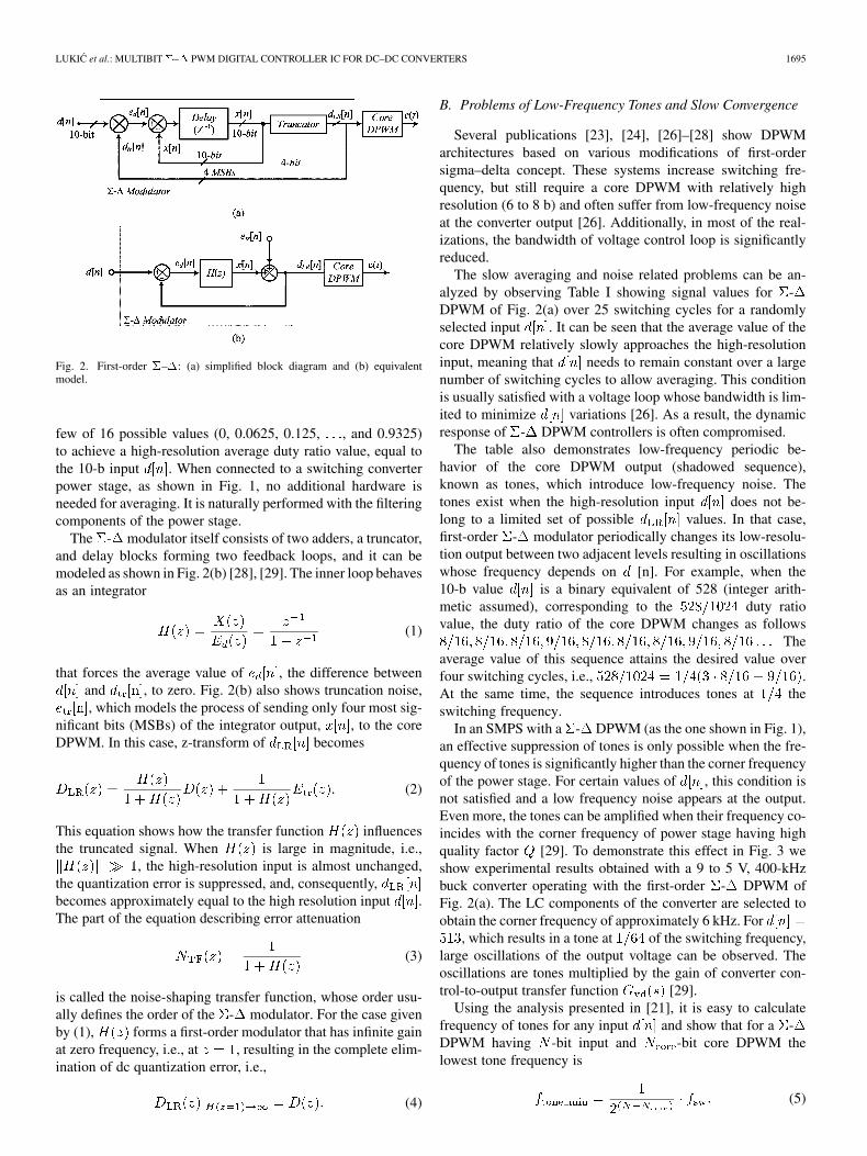
Fig. 2. First-order �–�: (a) simplified block diagram and (b) equivalentmodel.
few of 16 possible values (0, 0.0625, 0.125, , and 0.9325)to achieve a high-resolution average duty ratio value, equal tothe 10-b input . When connected to a switching converterpower stage, as shown in Fig. 1, no additional hardware isneeded for averaging. It is naturally performed with the filteringcomponents of the power stage.
The - modulator itself consists of two adders, a truncator,and delay blocks forming two feedback loops, and it can bemodeled as shown in Fig. 2(b) [28], [29]. The inner loop behavesas an integrator
(1)
that forces the average value of , the difference betweenand , to zero. Fig. 2(b) also shows truncation noise,, which models the process of sending only four most sig-
nificant bits (MSBs) of the integrator output, , to the coreDPWM. In this case, z-transform of becomes
(2)
This equation shows how the transfer function influencesthe truncated signal. When is large in magnitude, i.e.,
, the high-resolution input is almost unchanged,the quantization error is suppressed, and, consequently,becomes approximately equal to the high resolution input .The part of the equation describing error attenuation
(3)
is called the noise-shaping transfer function, whose order usu-ally defines the order of the - modulator. For the case givenby (1), forms a first-order modulator that has infinite gainat zero frequency, i.e., at , resulting in the complete elim-ination of dc quantization error, i.e.,
(4)
B. Problems of Low-Frequency Tones and Slow Convergence
Several publications [23], [24], [26]–[28] show DPWMarchitectures based on various modifications of first-ordersigma–delta concept. These systems increase switching fre-quency, but still require a core DPWM with relatively highresolution (6 to 8 b) and often suffer from low-frequency noiseat the converter output [26]. Additionally, in most of the real-izations, the bandwidth of voltage control loop is significantlyreduced.
The slow averaging and noise related problems can be an-alyzed by observing Table I showing signal values for -DPWM of Fig. 2(a) over 25 switching cycles for a randomlyselected input . It can be seen that the average value of thecore DPWM relatively slowly approaches the high-resolutioninput, meaning that needs to remain constant over a largenumber of switching cycles to allow averaging. This conditionis usually satisfied with a voltage loop whose bandwidth is lim-ited to minimize variations [26]. As a result, the dynamicresponse of - DPWM controllers is often compromised.
The table also demonstrates low-frequency periodic be-havior of the core DPWM output (shadowed sequence),known as tones, which introduce low-frequency noise. Thetones exist when the high-resolution input does not be-long to a limited set of possible values. In that case,first-order - modulator periodically changes its low-resolu-tion output between two adjacent levels resulting in oscillationswhose frequency depends on [n]. For example, when the10-b value is a binary equivalent of 528 (integer arith-metic assumed), corresponding to the duty ratiovalue, the duty ratio of the core DPWM changes as follows
Theaverage value of this sequence attains the desired value overfour switching cycles, i.e., .At the same time, the sequence introduces tones at theswitching frequency.
In an SMPS with a - DPWM (as the one shown in Fig. 1),an effective suppression of tones is only possible when the fre-quency of tones is significantly higher than the corner frequencyof the power stage. For certain values of , this condition isnot satisfied and a low frequency noise appears at the output.Even more, the tones can be amplified when their frequency co-incides with the corner frequency of power stage having highquality factor [29]. To demonstrate this effect in Fig. 3 weshow experimental results obtained with a 9 to 5 V, 400-kHzbuck converter operating with the first-order - DPWM ofFig. 2(a). The LC components of the converter are selected toobtain the corner frequency of approximately 6 kHz. For
, which results in a tone at of the switching frequency,large oscillations of the output voltage can be observed. Theoscillations are tones multiplied by the gain of converter con-trol-to-output transfer function [29].
Using the analysis presented in [21], it is easy to calculatefrequency of tones for any input and show that for a -DPWM having -bit input and -bit core DPWM thelowest tone frequency is
(5)

1696 IEEE TRANSACTIONS ON POWER ELECTRONICS, VOL. 22, NO. 5, SEPTEMBER 2007
TABLE ISTATES OF THE SIGNALS OF A FIRST-ORDER SIGMA–DELTA DPWM AND AVERAGE DUTY RATIO VALUE CALCULATED OVER N SWITCHING CYCLES
Fig. 3. Output voltage of experimental converter affected by low-frequencytones of first-order�-� PWM. Ch1 (ac-100 mV/div): output voltage; Ch2 (dc-5V/div): PWM signal c(t).
This equation also explains why in most of the existing -architectures [23]–[26] only a modest improvement of the coreDPWM resolution is achieved. To eliminate the noise, the differ-ence between the effective and core resolution ( of (5))is minimized keeping the tones at frequencies higher than powerstage corner frequency. It should be noted that the negative ef-fect of low-frequency tones usually cannot be eliminated with afaster voltage loop. As described above, such an attempt wouldcause faster changes, degradation of effective DPWM res-olution, and undesirable limit cycling of the compensator [11].
C. Second-Order Sigma–Delta DPWM
The problems of slow convergence toward high-resolutioninput and low-frequency tones existing in first-order - modu-lators have been extensively analyzed in research related to over-sampling ADCs and digital-to-analog converters (DACs) [21],
[30]. It has been shown that second-order - architecturesstrongly suppress low-frequency tones and have faster conver-gences. In the switching converter presented in [32], these ad-vantages are recognized and a single-bit analog second-order
- modulator is effectively used to improve output regulationof a pulse-train digital controller by spreading the spectrum ofits output voltage ripple. This single-bit system still operates ata variable switching frequency that increases the current stressof power stage components and, consequently, requires largerand slower semiconductor switchers.
In this paper, we show a new second-order multibit -DPWM architecture that allows operation at programmableconstant switching frequencies. The second-order multibit
- DPWM also minimizes the abovementioned tone-relatedproblems of first-order architectures allowing the use of alow-resolution low-power core DPWM to achieve switchingfrequencies beyond 10 MHz.
The design of second-order multibit - DPWM, shown inFig. 6, is inspired by power DAC [24], [25] architectures. How-ever, the main difference is in the system complexity. Since theDPWM does not require a very fast power-consuming ADC infeedback path (in this case only a truncated signal is sent back)its implementation is significantly simpler, and can be fully re-alized with digital components.
The system of Fig. 4 is a 10-b second-order sigma–delta witha 4-b core DPWM. Compared to the previously shown first-order implementation the main difference is in transfer function
(z) [Fig. 2(b)]. In this case, two delay blocks, an adder, andmultiplier form the discrete-time transfer function
(6)

LUKIC et al.: MULTIBIT – PWM DIGITAL CONTROLLER IC FOR DC–DC CONVERTERS 1697
Fig. 4. Block diagram of a 10-b, second-order, �-� DPWM having 4-b core.
Fig. 5. Output of experimental switching converter regulated withsecond-order �-� DPWM. Ch1 (ac-100 mV/div): Output voltage v (t);Ch2 (dc-5 V/div): PWM signal c(t).
which results in the desired second-order noise transfer functiondescribed with (3).
The effect of the second-order sigma–delta on the tonessuppression can be explained through the well-known noiseshaping analysis [21], [30]. It shows that a second-order systemmoves the truncation noise, and consequently, tones to higherfrequencies where the attenuation of the output low-pass filteris stronger.
To demonstrate positive effect of the second-order -DPWM in the experimental system described in Section I-B,the first-order - DPWM is replaced with the system ofFig. 4. The waveforms of Fig. 5 demonstrate that the low-fre-quency tones shown in Fig. 3 are almost completely eliminatedeven though the resolution of the core DPWM is still low (4 b).
The noise-shaping analysis can also be used to show thatthe effective resolution of a second-order sigma–delta DPWM,which is clocked at the switching frequency , is [30]
(7)
where is the time rate at which the high-resolution input is updated. Accordingly, for the system ofFig. 4, should be updated at 8 to achieveeffective resolution of 10 b using 4-b core DPWM.
Alternatively, the influence of the second-order - can beobserved through a comparison of its response to a step change
with the same response of a first-order - DPWM. Thisprocess is described with the following equations and corre-sponding diagrams of Fig. 6(a) and (b).
Let us assume that the following step input:
(8)
(a)
(b)
Fig. 6. Signal waveforms of a (a) first-order�-�DPWM and (b) second-ordersigma–delta DPWM.
is applied to the inputs of a first-order and a second-order -DPWM. The initial value belongs to the limited set ofpossible low-resolution core DPWM inputs, and then, a stepequal to least significant bits of occurs. It is also assumedthat the increment is smaller than the quantization step of thecore DPWM,
(9)

1698 IEEE TRANSACTIONS ON POWER ELECTRONICS, VOL. 22, NO. 5, SEPTEMBER 2007
where, as mentioned earlier, is the number of bits of .This type of step function is selected to simplify the analysis.The same results can be easily obtained for any other step andinitial condition.
A signal-flow analysis of the system illustrated in Fig. 2(a)shows that the inner loop output and change asfollows:
(10)
(11)
Since for , and for
(12)
It can be seen that for the first-order system changes lin-early, at the rate proportional to value . This process continuesuntil reaches or exceeds the first successive quantizationstep of the core DPWM, . At the time DPWMoutput changes, becomes negative and starts rampingdown with the slope . As shown in Fig. 6(a),the process is periodical and DPWM output always changes be-tween two adjacent values.
A similar analysis can be performed for the second-order- DPWM. It shows that
(13)
and that sequence changes as follows:
(14)
The rate of change described with the previous equation is muchfaster than that of the first-order - and, as shown in Fig. 6(b),in some instances the steps are larger than . As a result,the changes of the core DPWM are more frequent and larger inamplitude. Consequently, higher frequency tones are producedand faster averaging process is achieved.
Even though the variations of the duty ratio are stronger, theireffect on the switching converter output voltage is smaller, asshown in the previous experiments. This is because the largestportion of the tones energy is contained at frequencies signif-icantly higher than the power stage corner frequency where astrong attenuation is possible.
It should be noted that in a second-order - modulatora tradeoff between the reduction of the core DPWM resolu-tion and the amount of low-frequency tones introduced in thesystem exists as well, although significantly less severe thenin the first-order case. The tradeoff is a complex function ofthe - modulator parameters and its operating point and itsanalysis is usually challenging [30]. To ensure that the effect ofquantization noise is negligible, a help of widely available sim-ulation tools is usually advisable [21].
In this case, to verify satisfactory operation of the system, asweep analysis of output noise value for all possible inputscan be performed. Consequently, the minimum allowable coreDPWM resolution for a limited value of the output voltage noisecan be found in a relatively simple manner.
D. Practical Implementation
To minimize size and power consumption, the second-order- DPWM of Fig. 4 is modified and realized as shown in
Figs. 7(a) and (b) Instead of using 10-b signal , the –modulator processes the truncation error only. This structureis known as error-feedback [21], [30] and performs the samefunction as the above described second-order system utilizingmuch simpler digital hardware. In this case, only two addersare used, and and are just six least significant bits(LSBs) and four MSBs of , respectively. In addition, eachdelay block is realized with only six D flip-flops and the sizesof the adders are reduced accordingly. The 2 multiplicationblock is implemented as a simple 7-b logic shifter. The functionof the limiter is to restrict to positive values and preventoverflows.
The modulator is clocked at the switching frequency, bya signal created with the core DPWM. The 4-b core DPWMis based on the ring-oscillator architecture [13], [14], [22]consisting of sixteen digitally programmable delay cells, a16:1 multiplexer, and an – latch. The programmable delaycells provide regulation of switching frequency through signal
, which is either created externally or by a frequencymatching block, which is described in the following subsection.
At this point it might be interesting to compare the two pre-sented - architectures (first and second order) with a DPWMusing programmable digital dither [11], [31]. Similarly to thefirst-order - , the dithering DPWM varies the duty ratio ofa core-resolution DPWM by an LSB to improve the effectiveresolution. The dithering sequence, stored in a lookup table,is programmed such that for any given input it results in theminimum possible low-frequency ripple [31]. As a result, theoverall ripple of the dithering DPWM is smaller than that of thefirst-order - DPWM, which does not always produce the op-timum sequence. However, for several critical duty-ratio values,including the one described in the example of Section II-B, bothmethods produce the same low-frequency tones [31]. Hence,they have the same limitations regarding the selection of the res-olution of the core DPWM. Since the second-order - DPWM
LUKIC et al.: MULTIBIT – PWM DIGITAL CONTROLLER IC FOR DC–DC CONVERTERS 1699
Fig. 7. Error-feedback second-order �-� DPWM: (a) functional block diagram and (b) practical implementation.
pushes all tones to higher frequencies a more power efficient im-plementation of the core DPWM is possible. The second-order
- modulator also eliminates the need for a relatively largelook-up table of b [11], [31], used to storethe optimal dithering sequences. This on-chip area saving comesat the expense of larger power consumption of the modulatorpart itself, caused by relatively large adders operating at theswitching frequency. However, as shown in Section V, this con-sumption is practically negligible compared to the power takenby the core DPWM.
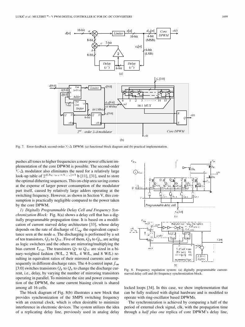
1) Digitally Programmable Delay Cell and Frequency Syn-chronization Block: Fig. 8(a) shows a delay cell that has a dig-itally programmable propagation time. It is based on a modifi-cation of current starved delay architecture [33], whose delaydepends on the rate of discharge of , the equivalent capaci-tance seen at the node . The discharging is performed by a setof ten transistors, to . Five of them, to , are actingas logic switchers and the others are mirroring/multiplying thebias current . The transistors to are sized in a bi-nary-weighted fashion (W/L, 2 W/L, 4 W/L, and 8 W/L) re-sulting in equivalent ratios of their mirrored currents and con-sequently in different discharge rates. The 4-b control input[3:0] switches transistors to to change the discharge cur-rent, i.e., delay, by varying the number of mirroring transistorsoperating in parallel. To minimize the size and power consump-tion of the DPWM, the same current biasing circuit is sharedamong all 16 cells.
The block diagram of Fig. 8(b) illustrates a new block thatprovides synchronization of the SMPS switching frequencywith an external clock, which is often desirable to minimizeinterference in electronic devices. The system utilizes the ideaof a replicating delay line, previously used in analog delay
Fig. 8. Frequency regulation system: (a) digitally programmable current-starved delay cell and (b) frequency synchronization block.
locked loops [34]. In this case, we show implementation thatcan be fully realized with digital hardware and is modified tooperate with ring-oscillator based DPWMs.
The synchronization is achieved by comparing a half of theperiod of external clock signal, clk, with the propagation timethrough a half plus one replica of core DPWM’s delay line,

1700 IEEE TRANSACTIONS ON POWER ELECTRONICS, VOL. 22, NO. 5, SEPTEMBER 2007
having delay cells, where is the number of delay el-ements of the core DPWM. Initially, at a rising edge of the clockstart signal is created and passed through the replica, whose lasttwo cells, i.e., and , are connected to two edgetriggered flip-flops. Then, at the immediately following negativeedge of the clock, strobe signal is created and a “snapshot” ofthose two delay cells is taken by D flip-flops. The snapshot isthen processed with the incremental logic block. Two logic ze-roes show a slower propagation (i.e., longer switching period)and increase the value of frequency control register [3:0].Similarly, two ones indicate a lower switching frequency andcause decrease of [3:0]. It is assumed that half periods ofDPWM and external clock are approximately equal when the bi-nary combination 10 occurs. In this case, an external clock withexact 50% duty ratio is required. For the case when a nonidealclock signal is applied the present circuit needs a minor modifi-cation. Then, the delay line can be replaced with a larger replicacontaining cells, and the start and the strobe signal needto be created with two successive rising or falling edges of theclock signal.
It should be noted that all-digital implementation of pro-grammable frequency DPWM and synchronization blocks isalso possible. It is more suitable when custom mixed-signaldesign of delay cells is not possible (FPGA implementationfor instance) or when the controller current consumption mea-sured in microamps is not crucial. In that case, the digitallyprogrammable current starved delay cells can be replaced witha structure consisting of a multiplexer and digital logic gatesacting as delay cells [8].
III. DUAL-MODE COMPENSATOR
To minimize power consumption of the compensator andmake it suitable for operation with the previously described
- DPWM, we developed a dual-mode PID compensatorarchitecture that can also be used with other DPWM topologies.
Previous analysis showed that in order to achieve high effec-tive resolution of a - DPWM its input needs to be updated atthe rate significantly lower than the switching frequency of theconverter. This implies that a successful realization of the pro-posed structure requires a slow compensator that would changecontrol value slowly, and in that way eliminate possiblenoise problems. However, this solution compromises the dy-namic performance of the switching converter and result in poortransient response.
The dual-mode architecture, shown in Fig. 9(a), consists ofa mode-control logic block and dual-mode compensator, whichis based on look-up tables (LUTs). This design utilizes the factthat high DPWM resolution is necessary in steady state only,while during transients it can be reduced to improve controllerresponse. Depending on the value of output voltage error(Fig. 1) mode control logic resolves whether the SMPS is insteady state or going through a transient and changes the modeof operation accordingly.
The mode change is performed through mode control signal.In steady state, the controller operates in under-sampled mode,where the frequency of PID compensator clock signal, , isreduced and a new value of duty ratio control variable iscalculated and updated slowly using slow mode set of look-up
Fig. 9. Block diagram of dual-mode PID compensator.
Fig. 10. State-transition diagram of mode control logic.
tables. This allows sufficiently long - averaging process, i.e.,results in high effective DPWM resolution, and significantly re-duced power consumption of the controller. During transientsthe clock is changed, is updated once per switching cycle,and faster LUT based compensator (Dyn mode PID of Fig. 9)is used to achieve fast transient response.
The LUT-based PID compensators employ discrete-timecontrol laws that can be described with the following generalequation:
(15)
In both modes, the same adders and registers are used to calcu-late and keep previous values of error and output variable,
and , respectively. The compensatorcoefficients , and , i.e., tables entries, are determined in ac-cordance with the procedure described in [35].
A. Mode Control Logic
To eliminate potential stability problems related to dynamicswitching between different control modes [36] mode controllogic is developed. The operation of the mode control logic isdescribed with the state diagram shown in Fig. 10. Initially, itis assumed that the controller is in steady state, characterizedwith low value of mode signal and low clocking frequency ofthe PID compensator. It remains in this state as long as output
LUKIC et al.: MULTIBIT – PWM DIGITAL CONTROLLER IC FOR DC–DC CONVERTERS 1701
voltage variations are small, i.e., . Upon a strong distur-bance the error increases and the controller switches to dynamicmode. The dynamic mode is maintained until a sufficiently longsequence values occur indicating that the converter isin equilibrium again.
It should be noted that a simple hysteretic logic [27] that im-mediately switches in static mode when the error becomes zero(or lower than certain number) often causes stability problemsand, as such, is not an optimal solution for the dual-mode oper-ation. During transients, even though converter is not in steadystate instantaneous values of the output capacitor voltage canresult in a short sequence of zero errors. In that case, if con-ventional hysteretic logic is used a fault steady-state is recog-nized and the controller prematurely switches in the slow con-trol mode. Since the slow controller is not able to handle thetransient, the error becomes large again and a cyclic switchingbetween the modes occurs.
IV. NONLINEAR ANALOG-TO-DIGITAL CONVERTER
Windowed-based ADCs [13], [14], [37], [38] measuringthe output voltage only around the reference voltage, i.e., zeroerror bin, are proven to be efficient solutions for low-powerdigital controllers both in terms of power consumption andrequired on-chip area for implementation. Architectures basedon delay lines [15], [38] and ring oscillators [13], [37] are mostcommon examples. In these ADCs the conversion is performedwith voltage-controlled oscillators (VCOs) or through changesof propagation times of delay cells supplied by the measuredvoltage. The main drawback of these architectures is that thequantization step and conversion speed depend on the operatingpoint defined with reference voltage , resulting in variablegain and slower conversion times at low input voltages.
In low-power portable applications, besides having very lowpower consumption and short conversion time, the ADC is alsorequired to operate with continuously decreasing input voltages.The supply voltages of modern digital circuits are reducing con-stantly following rapid advances in IC implementation tech-nology. In order to eliminate the need for the redesign of dig-ital controllers each time characteristics of the supplied deviceschange, it is desirable to have an ADC, whose operation is un-affected with the change of .
To eliminate the problem of variable quantization steps self-strobe solution combining delay line, VCO, and digital calibra-tion logic is shown in [38]. In this system, the digital logic ef-fectively controls the size of quantization step but the problemsof the variable conversion time and operation at lower supplyvoltage have not been addressed.
In the solution presented in [13], a pMOS differential paireliminates the influence of operating point on the ADC opera-tion. The pair produces two currents, whose difference is pro-portional to output voltage error, that are used to control fre-quencies of two ring oscillators clocking counters. A digitalequivalent of the analog error is then created by comparingthe counters values every switching cycle. It was shown thatthis ADC operates effectively in a switching converter oper-ating at frequencies up to 1.5 MHz. The ADC consumes about75 A/MHz, most of it is taken by the counters and ring oscilla-tors, which are significantly less power efficient than delay lines.
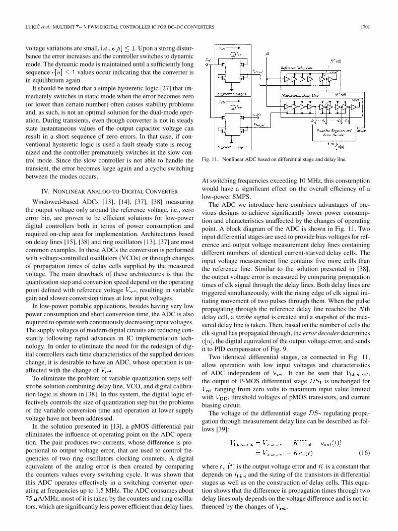
Fig. 11. Nonlinear ADC based on differential stage and delay line.
At switching frequencies exceeding 10 MHz, this consumptionwould have a significant effect on the overall efficiency of alow-power SMPS.
The ADC we introduce here combines advantages of pre-vious designs to achieve significantly lower power consump-tion and characteristics unaffected by the changes of operatingpoint. A block diagram of the ADC is shown in Fig. 11. Twoinput differential stages are used to provide bias voltages for ref-erence and output voltage measurement delay lines containingdifferent numbers of identical current-starved delay cells. Theinput voltage measurement line contains five more cells thanthe reference line. Similar to the solution presented in [38],the output voltage error is measured by comparing propagationtimes of clk signal through the delay lines. Both delay lines aretriggered simultaneously, with the rising edge of clk signal ini-tiating movement of two pulses through them. When the pulsepropagating through the reference delay line reaches the thdelay cell, a strobe signal is created and a snapshot of the mea-sured delay line is taken. Then, based on the number of cells theclk signal has propagated through, the error decoder determines
, the digital equivalent of the output voltage error, and sendsit to PID compensator of Fig. 9.
Two identical differential stages, as connected in Fig. 11,allow operation with low input voltages and characteristicsof ADC independent of . It can be seen that ,the output of P-MOS differential stage is unchanged for
ranging from zero volts to maximum input value limitedwith , threshold voltages of pMOS transistors, and currentbiasing circuit.
The voltage of the differential stage regulating propa-gation through measurement delay line can be described as fol-lows [39]:
(16)
where is the output voltage error and is a constant thatdepends on and the sizing of the transistors in differentialstages as well as on the construction of delay cells. This equa-tion shows that the difference in propagation times through twodelay lines only depends on the voltage difference and is not in-fluenced by the changes of .
1702 IEEE TRANSACTIONS ON POWER ELECTRONICS, VOL. 22, NO. 5, SEPTEMBER 2007
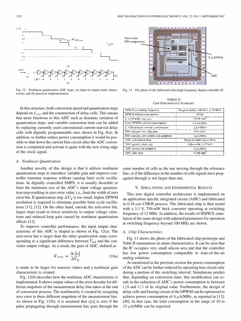
Fig. 12. Nonlinear quantization ADC steps: (a) input-to-output static charac-teristic and (b) practical implementation.
In this structure, both conversion speed and quantization stepsdepend on and the construction of delay cells. This meansthat more functions to this ADC such as dynamic variation ofquantization steps, and variable conversion time can be addedby replacing currently used conventional current-starved delaycells with digitally programmable ones shown in Fig. 8(a). Inaddition, to further reduce power consumption it would be pos-sible to shut down the current bias circuit after the ADC conver-sion is completed and activate it again with the new rising edgeof the clock signal.
A. Nonlinear Quantization
Another novelty of this design is that it utilizes nonlinearquantization steps to introduce variable gain and improve con-troller transient response without causing limit cycle oscilla-tions. In digitally controlled SMPS, it is usually desirable tolimit the minimum size of the ADC’s input voltage quantiza-tion step resulting in zero error value, i.e., limit the width of zeroerror bin. If quantization step is too small, higher DPWMresolution is required to eliminate possible limit cycle oscilla-tions [11], [12]. On the other hand, outside the zero-error bin,larger steps result in lower sensitivity to output voltage varia-tions and reduced loop gain caused by nonlinear quantizationeffects [12].
To improve controller performance, the input output char-acteristic of this ADC is shaped as shown in Fig. 12(a). Thezero-error bin is larger than the other quantization steps corre-sponding to a significant difference between and the con-verter output voltage. As a result, the gain of ADC, defined as
(16a)
is made to be larger for nonzero values and a nonlinear gaincharacteristic is created.
Fig. 12(b) describes how the nonlinear ADC characteristic isimplemented. It shows output values of the error decoder for dif-ferent snapshots of the measurement delay line taken at the endof conversion process. The nonlinearity is created by assigningzero error to three different snapshots of the measurement line.As shown in Fig. 12(b), it is assumed that is zero if thepulse propagating through measurement line goes through the
Fig. 13. Die photo of the fabricated ultra-high frequency digital controller IC.
TABLE IICHIP PERFORMANCE SUMMARY
same number of cells as the one moving through the referenceline, or if the difference in the number of cells signals have prop-agated through is not larger than one.
V. SIMULATIONS AND EXPERIMENTAL RESULTS
This new digital controller architecture is implemented onan application specific integrated circuit (ASIC) and fabricatedin 0.18- m CMOS process. The fabricated chip is then testedwith a 3.3 V, 750-mW buck converter operating at switchingfrequency of 12 MHz. In addition, the results of HSPICE simu-lation of the same design with adjusted parameters for operationat switching frequency beyond 100 MHz are shown.
A. Chip Characteristics
Fig. 13 shows die photo of the fabricated chip prototype andTable II summarizes its main characteristics. It can be seen thatthe IC occupies very small silicon area and that the controllerhas low power consumption comparable to state-of-the-artanalog solutions.
As mentioned in the previous section the power consumptionof the ADC can be further reduced by operating bias circuit onlyduring a portion of the switching interval. Simulations predictthat, depending on conversion time, this modification can re-sult in the reduction of ADC’s power consumption to between
and of its original value. Furthermore, the design ofdelay cells and biasing circuit of the DPWM can be optimized toachieve power consumption of 4 A/MHz, as reported in [13],[40]. In that case, the total consumption in the range of 10 to15 A/MHz can be expected.

LUKIC et al.: MULTIBIT – PWM DIGITAL CONTROLLER IC FOR DC–DC CONVERTERS 1703
Fig. 14. Output of experimental switching converter for gradual change of duty ratio control input d[n] from 0 to 1023. Left: without �-� modulator. Right:when the �-� modulator is active.
Fig. 15. Change of DPWM switching frequency through f [n] variations, Ch.1: PWM control signal c(t); D0 to D3: 4-b switching frequency control signalf [n].
B. Verification of Open-Loop Operation
Here, the results of functional verification of - DPWM op-eration are given. Fig. 14 demonstrates the effect of - mod-ulator on the effective DPWM resolution. It shows the output ofan experimental switching converter for a sweep change of dutyratio caused by slow incremental change of 10-b control input
[n], from 0 to 1023. The results are shown for two modes ofoperation, when the - modulator is disabled and when it isactive. It can be seen that, as described in Section II, the effectiveresolution of the core DPWM is significantly improved. In ad-dition it can be seen that the modulator improves linearity of theDPWM. Different propagation times of core DPWM delay cellscaused by process variation, parasitic capacitance of the chiplayout, and different loading of delay cells used for clock gen-eration cause nonuniform quantization steps of the core DPWM.Due to the operation of - , the variations of the delays are alsoaveraged and their effect is minimized.
It should be noted that the uniformity of the quantizationsteps of the core DPWM can be improved by loading all of
them equally, with additional buffer cells. However, this solu-tion would result in an increase of the equivalent capacitance ofcurrent starved delay cells [Fig. 8(a)] and consequently in higherpower consumption of the core DPWM.
Fig. 15 demonstrates operation of DPWM for the changeof frequency regulation signal [Fig. 8(b)] between twovalues. It can be seen that the frequency can be changed ina single switching cycle and that the DPWM can operate at18 MHz. This shows that if programmable delay cells havinghigher resolution are used this IC could potentially operate asa combined digital pulse-frequency/pulsewidth modulator aswell and, consequently, be used in quasi-resonant convertertopologies.
C. Closed-Loop Operation
To verify closed-loop operation a 6 to 3.3 V, 750-mW, buckpower stage was constructed and regulated by the controller ICas shown in Fig. 1. The switching frequency of the controller isintentionally reduced to 12.6 MHz to accommodate limitations

1704 IEEE TRANSACTIONS ON POWER ELECTRONICS, VOL. 22, NO. 5, SEPTEMBER 2007
Fig. 16. Steady-state operation of digital controller at 12.6-MHz switching frequency, Ch.1: Regulated output voltage at 3.3 V (500 mV/div); Ch.2: PWM controlsignal c(t) (2.5 V/div). Time scale is 50 ns/div.
Fig. 17. Results of load transient experiment. Ch.1: Regulated output voltage at 3.3 V (ac-200 mV/div); Ch.2: Load current; D5: compensator clock signal clk1(Fig. 9); D4: mode control signal; D0 to D3: 4-b binary error value e[n].
of currently available power stage components (commerciallyavailable inductors, gate drivers, and power MOSFET-s).
Fig. 16 demonstrates steady state operation of the closed-loopsystem. The diagrams show that the controller provides a well-regulated output voltage without limit cycle oscillations or noiserelated problems even though the resolution of the core DPWMis only 4 b. The waveforms also demonstrate how the modu-lator changes duty ratio value, i.e., time, through severalsuccessive switching cycles to achieve high effective DPWMresolution.
Fig. 17 shows results of a load transient response experi-ment for the output current change between 10 and 220 mAand demonstrates operation of the dual-mode PID controller de-scribed in Section III. Upon a load transient is recognized thecontroller switches to dynamic mode (frequency of shownin Fig. 9 is high). The controller remains in dynamic mode untilthe output voltage is stabilized, i.e., is small over a large
number of switching cycles. Then, it returns to steady-state con-trol mode, where the frequency of decreases. The resultsverify that dual-mode operation results in a fast load transientresponse.
D. Simulation Results
The fabricated IC is optimized to operate at switching fre-quencies between 1.5 and 20 MHz. In order to show that thesame structure can be used with upcoming power supplies oper-ating at even higher switching frequencies, we slightly modifiedthe actual IC design and simulated its operation at 150 MHz,using HSPICE. The switching frequency of - DPWM andthe conversion speed of the ADC are increased through differentsizing of current starved delay cells and adjustments of bias cur-rent of the circuits shown in Figs. 8(a) and 11, respectively.
The results of analog HSPICE simulation are shown inFigs. 18 and 19. Fig. 18 shows PWM waveforms of -
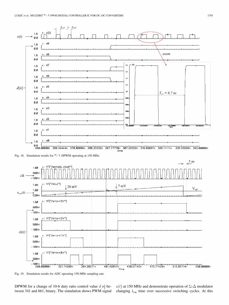
LUKIC et al.: MULTIBIT – PWM DIGITAL CONTROLLER IC FOR DC–DC CONVERTERS 1705
Fig. 18. Simulation results for �-� DPWM operating at 150 MHz.
Fig. 19. Simulation results for ADC operating 150-MHz sampling rate.
DPWM for a change of 10-b duty ratio control value be-tween 341 and 661, binary. The simulation shows PWM signal
at 150 MHz and demonstrate operation of - modulatorchanging time over successive switching cycles. At this

1706 IEEE TRANSACTIONS ON POWER ELECTRONICS, VOL. 22, NO. 5, SEPTEMBER 2007
frequency, the effective 10-b DPWM resolution correspondsto the equivalent time step of less than 7 ps. Due to limitedspeed, this time-step cannot be achieved with ring-oscillatoror counter based DPWM architectures using most commontechnologies for IC implementation. For example, typicalpropagation time of a 0.18- m CMOS digital logic cell isbetween 20 and 50 ps limiting maximum frequency/resolutionof the other architectures. The estimated current consumptionis 700 A, significantly smaller than what Table II predicts.This is because delay cells with smaller equivalent capacitance[Fig. 8(a)] are used to increase the switching frequency. Thereduced capacitance requires less energy to be charged andcauses shorter lasting shoot-through current through the outputCMOS stage of delay cells, both of which significantly reduceoverall power consumption.
The simulation results of Fig. 19 demonstrate operation of thenonlinear ADC when the clock signal frequency, provided bythe DPWM, is 150 MHz. The waveforms show how the rampingchange of switching converter output voltage, , around 1V reference influences ADC’s output, i.e., error . It can beseen that also ramps from the binary value to , for80-mV effective change of the converter input voltage. Nonuni-form quantization steps described in the previous section canalso be observed. The zero error bin of this ADC is around20 mV, approximately three times larger than the step corre-sponding to . Simulations also verify fast analog-to-digital conversion. It can be seen that he ADC needs only 5 ns toreact to an abrupt voltage change and convert analog signal intoits digital equivalent. The current consumption is about 950 A,because of the same reasons mentioned in the previous case, itis smaller than the value given in Table II.
These results verify that proposed architecture can provide aneffective digital control solution for the fastest switching powerconverters today, as well as for upcoming systems expected tooperate at frequencies beyond 100 MHz.
VI. CONCLUSION
A digital PWM controller IC for low-power dc–dc switchingconverters capable of operating at switching frequencies ex-ceeding 10 MHz is presented. To achieve the high frequency ofoperation, low power consumption and improved load transientresponse, the controller utilizes three novel architectures ofbasic functional blocks, second-order multibit - DPWM,dual-mode PID compensator, and nonlinear ADC. It is shownhow the second-order - modulator eliminates tone relatedproblems occurring in first-order - DPWM architecturesand consequently allows a significant increase of switchingfrequency and effective DPWM resolution. The dual-modePID compensator operating at a sampling rate lower thanswitching frequency in steady state, and at the switching rateduring transients, is developed to minimize overall powerconsumption without sacrificing transient response. The ADCcombining dual differential input stage, delay lines, and non-linear error logic is introduced as well. It allows operation withinput voltages as low as zero volts and has quantization stepsand conversion time independent of the operating point. Thenonlinear error logic additionally improves dynamic response
by creating nonuniform quantization steps that increase gain ofthe ADC for nonzero output voltage errors.
The new controller architecture is implemented on a 0.18 mCMOS integrated circuit and operation of the - DPWM atprogrammable constant switching frequencies up to 16 MHz isdemonstrated. The fabricated IC exhibits low current consump-tion of 55 A/MHz. Operation in closed loop with an experi-mental 12.4 MHz, 6 to 3.3 V, 750-mW buck converter is demon-strated and good transient response performance is verified aswell. Furthermore, the same design is modified to operate athigher switching frequencies and tested through simulations. Itis shown that this digital architecture offers potential solutionfor controlling upcoming low-power switching converters thatare likely to operate at switching frequencies beyond 100 MHz.
REFERENCES
[1] A. V. Peterchev and S. R. Sanders, “Digital multimode buck convertercontrol with loss-minimizing synchronous rectifier adaptation,” IEEETrans. Power Electron., vol. 21, no. 6, pp. 1588–1599, Nov. 2006.
[2] V. Yousefzadeh and D. Maksiomivic, “Sensorless optimization of deadtimes in dc–dc converters with synchronous rectifiers,” IEEE Trans.Power Electron., vol. 21, no. 4, pp. 994–1002, Jul. 2006.
[3] A. Prodic and D. Maksimovic, “Digital PWM controller and current es-timator for a low-power switching converter,” in Proc. IEEE COMPELConf., 2000, pp. 123–128.
[4] W. Stefanutti, P. Mattavelli, S. Saggini, and M. Ghioni, “Autotuning ofdigitally controlled buck converters based on relay feedback,” in Proc.IEEE PESC Conf., 2005, pp. 2140–2145.
[5] B. Miao, R. Zane, and D. Maksimovic, “System identification of powerconverters with digital control through cross-correlation methods,”IEEE Trans. Power Electron., vol. 20, no. 5, pp. 1093–1099, Sept.2005.
[6] A. L. Kelly and K. Rinne, “A self-compensating adaptive digital reg-ulator for switching converters based on linear prediction,” in Proc.IEEE APEC Conf., 2006, pp. 712–718.
[7] Z. Zhao, H. Lee, A. Feizmohammad, and A. Prodic, “Limit-cycle basedauto-tuning system for digitally controlled low-power SMPS,” in Proc.IEEE APEC Conf., 2006, pp. 1143–1147.
[8] A. Prodic, D. Maksimovic, and R. W. Erickson, “Digital controller chipset for isolated DC power supplies,” in Proc. IEEE APEC Conf., 2003,pp. 866–872.
[9] A. Soto, P. Alou, and J. A. Cobos, “Non-linear digital control breaksbandwidth limitations,” in Proc. IEEE APEC Conf., 2006, pp. 724–730.
[10] A. P. Chandrakasan and R. W. Brodersen, “Minimizing power con-sumption in digital CMOS circuits,” Proc. IEEE, vol. 83, no. 4, pp.498–523, Apr. 1995.
[11] A. V. Peterchev and S. R. Sanders, “Quantization resolution and limitcycling in digitally controlled PWM converters,” IEEE Trans. PowerElectron., vol. 18, no. 1, pp. 301–308, Jan. 2003, Special Issue on Dig-ital Control.
[12] H. Peng, A. Prodic, E. Alarcon, and D. Maksimovic, “Modeling ofquantization effects in digitally controlled dc–dc converters,” IEEETrans. Power Electron., vol. 22, no. 1, pp. 208–215, Jan. 2007.
[13] J. Xiao, A. Peterchev, J. Zhang, and S. R. Sanders, “A 4-�A quies-cent-current dual-mode digitally controlled buck converter IC for cel-lular phone applications,” IEEE J. Solid-State Circ., vol. 39, no. 12, pp.2342–2348, Dec. 2004.
[14] A. P. Dancy and A. P. Chandrakasan, “Ultra low power control circuitsfor PWM converters,” in Proc. IEEE PESC Conf., 1997, pp. 21–27.
[15] B. Patella, A. Prodic, A. Zirger, and D. Maksimovic, “High-frequencydigital controller PWM controller IC for dc–dc converters,” IEEETrans. Power Electron., vol. 18, no. 1, pp. 438–446, Jan. 2003, SpecialIssue on Digital Control.
[16] R. Foley, R. Kavanagh, W. Marnane, and M. Egan, “Mutiphase digitalpulsewidth modulator,” IEEE Trans. Power Electron., vol. 21, no. 3,pp. 842–846, May 2006.
[17] Data Sheet MAX 85600, 500 mA, 4 MHz, Step-Down DC–DC Con-verter, Maxim, Inc.
[18] C. E. Mullett, “A 5-year power technology roadmap,” in Proc. IEEEAPEC Conf., 2004, pp. 11–17.
[19] M. Gaye, S. Ajram, J. Y. Lebas, R. Kozlowski, and G. Salmer, “A50–100 MHz 5 V to �5 V, 1 W Cuk converter using gallium arsenidepower switches,” in Proc. IEEE ISCAS Conf., 2000, pp. 264–267.

LUKIC et al.: MULTIBIT – PWM DIGITAL CONTROLLER IC FOR DC–DC CONVERTERS 1707
[20] E. O’Malley and K. Rinne, “A programmable digital pulse widthmodulator providing versatile pulse patterns and supporting switchingfrequencies beyond 15 MHz,” in Proc. IEEE APEC Conf., 2004, pp.53–59.
[21] R. Schreirar and G. C. Temes, Understanding Delta-Sigma Data Con-verters. New York: Wiley, 2005.
[22] A. Syed, E. Ahmed, D. Maksimovic, and E. Alarcon, “Digital pulsewidth modulator architectures,” in Proc. IEEE PESC’04 Conf., 2004,pp. 4689–4695.
[23] K. M. Smith, K. M. Smedley, and M. Yunhong Ma, “Realization of adigital PWM power amplifier using noise and ripple shaping,” in Proc.IEEE PESC Conf., 1995, pp. 96–102.
[24] J. M. Goldberg and M. B. Sandler, “New high accuracy pulse widthmodulation based digital-to-analogue convertor/power amplifier,” inIEE Proc. Circ. Devices and Sys., Aug. 1994, no. 4, pp. 315–324.
[25] A. J. Magrath and M. B. Sandler, “Hybrid pulse width modulation/sigma-delta modulation power digital-to-analogue converter,” in IEEProc. Circ. Devices and Sys., Jun. 1996, no. 3, pp. 149–156.
[26] Z. Lu, Z. Qian, Y. Zeng, W. Yao, G. Chen, and Y. Wang, “Reductionof digital PWM limit ring with novel control algorithm,” in Proc. IEEEAPEC Conf., 2001, pp. 521–525.
[27] Z. Lukic, K. Wang, and A. Prodic, “High-frequency digital controllerfor dc–dc converters based on multi-bit sigma–delta pulse-width mod-ulation,” in Proc. IEEE APEC Conf., 2005, pp. 35–40.
[28] A. Kelly and K. Rinne, “High resolution DPWM in a dc–dc converterapplication using digital sigma–delta techniques,” in Proc. IEEE PESCConf., 2005, pp. 1458–1463.
[29] R. W. Erickson and D. Maksimovic, Fundamentals of Power Elec-tronics, 2nd ed. Boston, MA: Kluwer, 2000, pp. 265–322.
[30] D. A. Johns and K. Martin, Analog Integrated Circuit Design. NewYork: Wiley, 1997, pp. 531–571.
[31] A. V. Peterchev, “Digital Pulse-Width Modulation Control in PowerElectronics Circuits: Theory and Application,” Ph.D. dissertation,Berkeley, CA, Jun. 2005.
[32] S. K. Dunlap and T. S. Fiez, “A noise-shaped switching power supplyusing a delta-sigma modulator,” IEEE Trans. Circuits Syst., vol. 51, no.6, pp. 1051–1061, Jun. 2004.
[33] M. Maymandi-Nejad and M. Sachdev, “A digitally programmabledelay element: Design and analysis,” IEEE Trans. Very Large Scale(VLSI) Syst., vol. 11, pp. 871–878, Oct. 2003.
[34] Y. Moon, J. Choi, K. Lee, D. K. Jeong, and M. K. Kim, “An all-analogmultiphase delay-locked loop using a replica delay line for wide-rangeoperation and low-jitter performance,” IEEE J. Solid-State Circuits,vol. 35, no. 3, pp. 377–384, Mar. 2000.
[35] A. Prodic and D. Maksimovic, “Design of a digital PID regulator basedon look-up tables for control of high-frequency dc–dc converters,” inProc. IEEE COMPEL Conf., 2002, pp. 18–22.
[36] R. Hanus, M. Kinnaret, and J. L. Henrotte, “Conditioning techniques,a general anti-windup and bumpless transfer method,” Automatica, pp.729–739, 1987.
[37] G. Y. Wei and M. Horowitz, “A fully digital, energy-efficient, adaptivepower-supply regulator,” IEEE J. Solid-State Circuits, vol. 34, no. 4,pp. 520–528, Apr. 1999.
[38] M. Vincent and D. Maksimovic, “Matched Delay Line Voltage Con-verter,” U.S. Patent 6 958721, Oct. 2005.
[39] A. S. Sedra and K. C. Smith, Microelectronic Circuits, 5th ed. NewYork: Oxford Univ. Press, 2004.
[40] N. Rahman, A. Parayandeh, K. Wang, and A. Prodic, “Multimode dig-ital SMPS controller IC for low-power management,” in Proc. IEEEISCAS Conf., 2006.
Zdravko Lukic (S’04) was born in Novi Sad, Serbia,in 1980. He received the Dipl. Ing. degree in elec-trical engineering from the University of Novi Sad,Novi Sad, and the M.A.Sc. degree in electrical en-gineering from the University of Toronto, Toronto,ON, Canada, in 2003 and 2006, respectively. He ispresently pursuing the Ph.D. degree at the Laboratoryfor Low-Power Management and Integrated Switch-Mode Power Supplies, University of Toronto.
His research interests include digital controltechniques and low-power mixed-signal IC design
for high-frequency switch-mode power supplies.
Nabeel Rahman, photograph and biography not available at the time ofpublication.
Aleksandar Prodic (S’00–M’03) received the Dipl.Ing. degree in electrical engineering from the Univer-sity of Novi Sad, Novi Sad, Serbia, in 1994 and theM.Sc. and Ph.D. degrees from the Colorado PowerElectronics Center, University of Colorado, Boulder,in 2000 and 2003, respectively.
Since 2003, he has been with the University ofToronto, Toronto, ON, Canada, where he is an As-sistant Professor in the Department of Electrical andComputer Engineering. In 2004, at the University ofToronto, he established Laboratory for Low-Power
Management and Integrated Switch-Mode Power Supplies. His research inter-ests include digital control of low-power high-frequency SMPS, mixed-signalIC design, DSP techniques for power electronics, and the development ofsystems-on-chip (SoC) for power management.