Embed Size (px)
Citation preview

CHAPTER 1
INTRODUCTION
1.1 INTRODUCTION
Today, owing to availability of state-of-the-art microcontrollers and digital signal
processors (DSPs), complex control algorithms can be easily implemented to attain the
desired system performance. But in actual control systems, it is difficult to attain the
expected result for various factors affect the control systems such as control algorithms
itself, capability of controllers, capability of implement equipment and states of control
circumstance. Except those factors, communication parameters of control systems
including Baud Rate, BER (Bit Error Rate) and synchronization between sub-systems
also engender great effect. In order to improve precision of control system and make
good use of modern control algorithms, we should pay much more attention on
communication in control systems.
The UART: What it is and how it works
The Universal Asynchronous Receiver/Transmitter (UART) controller is the key
component of the serial communications subsystem of a computer. The UART takes
bytes of data and transmits the individual bits in a sequential fashion. At the destination, a
second UART re-assembles the bits into complete bytes. Serial transmission is commonly
used with modems and for non-networked communication between computers, terminals
and other devices. There are two primary forms of serial transmission: Synchronous and
Asynchronous. Depending on the modes that are supported by the hardware, the name of
the communication sub-system will usually include if it supports asynchronous
communications and a S if it supports synchronous communications. Both forms are
described below. Some common acronyms are:
UART Universal Asynchronous Receiver/Transmitter
USART Universal Synchronous-Asynchronous Receiver/Transmitter
Synchronous Serial Transmission
1

Synchronous serial transmission requires that the sender and receiver share a
clock with one another, or that the sender provide a strobe or other timing signal so that
the receiver knows when to “read” the next bit of the data. In most forms of serial
synchronous communication, if there is no data available at a given instant to transmit, a
fill character must be sent instead so that data is always being transmitted. Synchronous
communication is usually more efficient because only data bits are transmitted between
sender and receiver, and synchronous communication can be more costly if extra wiring
and circuits are required to share a clock signal between the sender and receiver.
A form of synchronous transmission is used with printers and fixed disk devices
in that the data is sent on one set of wires while a clock or strobe is sent on a different
wire. Printers and fixed disk devices are not normally serial devices because most fixed
disk interface standards send an entire word of data for each clock or strobe signal by
using a separate wire for each bit of the word. In the PC industry, these are known as
Parallel devices. The standard serial communications hardware in the PC does not
support synchronous operations. This mode is described here for comparison purposes
only.
Asynchronous Serial Transmission
Asynchronous transmission allows data to be transmitted without the sender
having to send a clock signal to the receiver. Instead, the sender and receiver must agree
on timing parameters in advance and special bits are added to each word which are used
to synchronize the sending and receiving units.
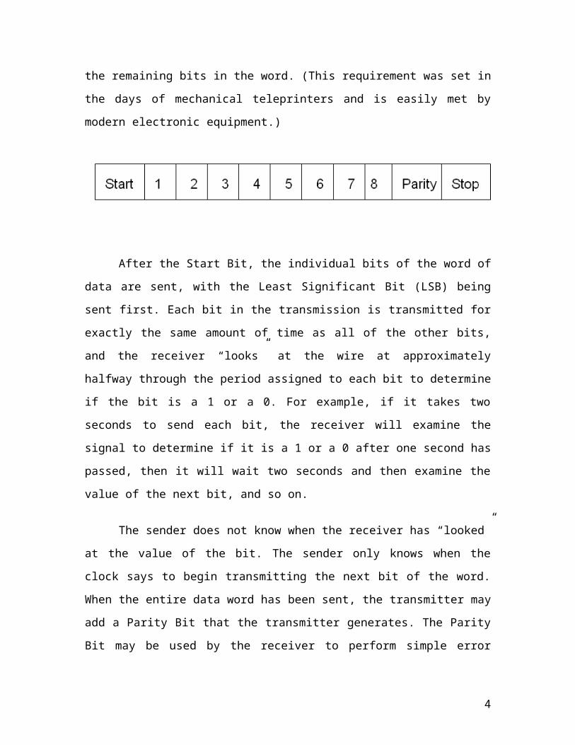
When a word is given to the UART for Asynchronous transmissions, a bit called
the "Start Bit" is added to the beginning of each word that is to be transmitted. The Start
Bit is used to alert the receiver that a word of data is about to be sent, and to force the
clock in the receiver into synchronization with the clock in the transmitter. These two
clocks must be accurate enough to not have the frequency drift by more than 10% during
the transmission of the remaining bits in the word. (This requirement was set in the days
of mechanical teleprinters and is easily met by modern electronic equipment.)
2

After the Start Bit, the individual bits of the word of data are sent, with the Least
Significant Bit (LSB) being sent first. Each bit in the transmission is transmitted for
exactly the same amount of time as all of the other bits, and the receiver “looks” at the
wire at approximately halfway through the period assigned to each bit to determine if the
bit is a 1 or a 0. For example, if it takes two seconds to send each bit, the receiver will
examine the signal to determine if it is a 1 or a 0 after one second has passed, then it will
wait two seconds and then examine the value of the next bit, and so on.
The sender does not know when the receiver has “looked” at the value of the bit.
The sender only knows when the clock says to begin transmitting the next bit of the
word. When the entire data word has been sent, the transmitter may add a Parity Bit that
the transmitter generates. The Parity Bit may be used by the receiver to perform simple
error checking. Then at least one Stop Bit is sent by the transmitter.
When the receiver has received all of the bits in the data word, it may check for
the Parity Bits (both sender and receiver must agree on whether a Parity Bit is to be
used), and then the receiver looks for a Stop Bit. If the Stop Bit does not appear when it is
supposed to, the UART considers the entire word to be garbled and will report a Framing
Error to the host processor when the data word is read. The usual cause of a Framing
Error is that the sender and receiver clocks were not running at the same speed, or that the
signal was interrupted.
Regardless of whether the data was received correctly or not, the UART
automatically discards the Start, Parity and Stop bits. If the sender and receiver are
configured identically, these bits are not passed to the host. If another word is ready for
transmission, the Start Bit for the new word can be sent as soon as the Stop Bit for the
3
previous word has been sent. Because asynchronous data is “self synchronizes”, if there
is no data to transmit, the transmission line can be idle.
Other UART Functions
In addition to the basic job of converting data from parallel to serial for
transmission and from serial to parallel on reception, a UART will usually provide
additional circuits for signals that can be used to indicate the state of the transmission
media, and to regulate the flow of data in the event that the remote device is not prepared
to accept more data. For example, when the device connected to the UART is a modem,
the modem may report the presence of a carrier on the phone line while the computer
may be able to instruct the modem to reset itself or to not take calls by raising or lowering
one more of these extra signals. The function of each of these additional signals is
defined in the EIA RS232-C standard.
Multi Channel UART
The Multi Channel Uart Contains more than one transmit/receive per uart. All
the channels can operate independently or together. Data can be received on one and
transmitted on other and also the data rate on different channels can be same or different.
The channels of the Multi channel uart are designed to reduce the CPU overhead when
working with high speed modems and other devices. Here we are implementing a multi
channel Uart which contains 4 Uarts.
This multi channel uart operates in three modes one is Normal mode, second is
Hub mode and last is Bridge Mode. In Normal mode all these Uarts are completely
independent in functionality, but share common logic to reduce its overall size as
compared to individual instantiations. In Hub mode the data received by the uart will be
transmit by the other uarts. In Bridge mode the data received by the Uart1is Transmitted
by the Uart2 and the data received by the Uart3 is transmitted by the Uart4. In this both
the Uarts operates at different Baud rates.
Each channel performs serial to parallel conversion on data characters received
from a peripheral device, and parallel to serial conversion on data characters received
4

from the CPU. The CPU can read the complete status of each channel at any time.
Synchronization for the serial data stream is accomplished by adding start and stop bits to
the transmit data to form a data character. An optional parity bit can be attached to the
data character to enhance Data integrity. The receiver checks the parity bit for any
transmission bit errors. Each channel has its own baud rate value, receive and transmit
FIFO and CPU registers. The user has control over the configuration of the core by
modifying the parameters in the top-level source file. This allows the core to be modified
and reused easily. These parameters include number of channels and FIFO depth.
1.2 VLSI
Very-large-scale integration (VLSI) is the process of creating integrated circuits
by combining thousands of transistor-based circuits into a single chip. VLSI began in the
1970s when complex semiconductor and communication technologies were being
developed. The microprocessor is a VLSI device. This is the field which involves
packing more and more logic devices into smaller and smaller areas. VLSI circuits can
now be put into a small space few millimeters across. This has opened up a big
opportunity to do things that were not possible before. VLSI circuits are everywhere ...
our computer, our car, our brand new state-of-the-art digital camera, the cell-phones, and
what we have.
VLSI has been around for a long time, there is nothing new about it ... but as a
side effect of advances in the world of computers, there has been a dramatic proliferation
of tools that can be used to design VLSI circuits. Alongside, obeying Moore's law, the
capability of an IC has increased exponentially over the years, in terms of computation
power, utilization of available area, yield. The combined effect of these two advances is
that people can now put diverse functionality into the IC's, opening up new frontiers.
Examples are embedded systems, where intelligent devices are put inside everyday
objects, and ubiquitous computing where small computing devices proliferate to such an
extent that even the shoes we wear may actually do something useful like monitoring our
heartbeats!
5
1.3 XILINX
Xilinx, Inc. (NASDAQ: XLNX) is the world’s largest supplier of programmable
logic devices, the inventor of the field programmable gate array (FPGA) and the first
semiconductor company with a fabless manufacturing model. The programmable
logic device market has been led by Xilinx since the late 1990s. Over the years, Xilinx
has fueled an aggressive expansion to India, Asia and Europe – regions Xilinx
representatives have described as high-growth areas for the business.
Xilinx has been repeatedly recognized as one of Fortune’s best places to work and
as the “Most Respected Public Fabless Company” by the Global Semiconductor Alliance.
The company’s products have been recognized by EE Times, EDN and others for
innovation and market impact.
The company has expanded its product portfolio substantially since its founding,
now selling a broad range of FPGAs, complex programmable logic devices (CPLD),
design tools, intellectual property and reference designs. Xilinx also has a global services
and training program. The organization’s most popular product lines (see Current Family
Lines) are the Spartan, Virtex and Easy Path series, each including configurations and
models optimized for different applications.
1.3.1 Technology
Xilinx designs, develops and markets programmable logic products including
integrated circuits (ICs), software design tools, predefined system functions delivered as
intellectual property (IP) cores, design services, customer training, field engineering and
technical support. Xilinx sells both FPGAs and CPLDs programmable logic devices for
electronic equipment manufacturers in end markets such as communications, industrial,
consumer, automotive and data processing.
Xilinx’s FPGAs have even been used for the ALICE (A Large Ion Collider
Experiment) at the CERN European laboratory on the French-Swiss border to map and
disentangle the trajectories of thousands of subatomic particles.
6

The Virtex-II Pro, Virtex-4, Virtex-5, and Virtex-6 FPGA families are particularly
focused on system-on-chip (SoC) designers because they include up to two embedded
IBM PowerPC cores. They can run a regular embedded OS (such as Linux or vxWorks)
and they can implement processor peripherals in programmable logic.
Xilinx’s IP cores include IP for simple functions (BCD encoders, counters, etc.),
for domain specific cores (digital signal processing, FFT and FIR cores) to complex
systems (multi-gigabit networking cores, Micro Blaze soft microprocessor, and the
compact Picoblaze microcontroller). Xilinx also creates custom cores for a fee.
The ISE Design Suite is the central electronic design automation (EDA) product
family sold by Xilinx. The ISE Design Suite features include design entry and synthesis
supporting Verilog or VHDL, place-and-route (PAR), completed verification and debug
using ChipScope Pro tools, and creation of the bit files that are used to configure the chip.
Xilinx’s Embedded Developer’s Kit (EDK) supports the embedded PowerPC 405
and 440 cores (in Virtex-II Pro and some Virtex-4 and -5 chips) and the Micro blaze core.
Xilinx’s System Generator for DSP implements DSP designs on Xilinx’s FPGAs. A
freeware version of its EDA software called ISE WebPACK is used with some of its non-
high-performance chips. Xilinx is the only (as of 2007) FPGA vendor to distribute a
native Linux freeware synthesis toolchain.
1.3.2 Current family lines
Xilinx has two main FPGA families: the high-performance Virtex series and the
high-volume Spartan series, with a cheaper Easy Path option for ramping to volume
production. It also manufactures two CPLD lines, the CoolRunner and the 9500 series.
Each model series has been released in multiple generations since its launch.
The latest Virtex-6 and Spartan-6 FPGA families are said to consume 50 percent
less power, cost 20 percent less, and have up to twice the logic capacity of previous
generations of FPGAs.
7

1.3.3 Spartan family
The Spartan series targets applications with a low-power footprint, extreme cost
sensitivity and high-volume such as displays, set-top boxes, wireless routers and other
applications. The Spartan-6 family is built on a 45-nanometer (nm), 9-metal layer, dual-
oxide process technology. The Spartan-6 was marketed in 2009 as a low-cost solution for
automotive, wireless communications, flat-panel display and video surveillance
applications.
The Spartan-3A consumes more than 70-90 percent less power in suspend mode
and 40-50 percent less for static power compared to standard devices. Also, the
integration of dedicated DSP circuitry in the Spartan series has inherent power
advantages of approximately 25 percent over competing low-power FPGAs.
1.3.4 Virtex family
The Virtex series of FPGAs have integrated features such as wired and wireless
infrastructure equipment, advanced medical equipment, test and measurement, and
defense systems. In addition to FPGA logic, the Virtex series includes embedded fixed
function hardware for commonly used functions such as multipliers, memories, serial
transceivers and microprocessor cores. The Virtex-6 family is built on a 40-nm process
for compute-intensive electronic systems, and the company claims it consumes 15
percent less power and has 15 percent improved performance over competing 40 nm
FPGAs.
The Virtex-II Pro family was the first to combine PowerPC embedded technology
(including single and multiple PowerPC 405 processor cores) and integrated serial
transceivers (up to 3.125 Gbps in Virtex-II Pro and up to 10.3125 in Virtex-II Pro X).
The Virtex-5 LX and the LXT are also intended for logic-intensive applications, and the
Virtex-5 SXT is for DSP applications. The Virtex-5 FXT has been described by Xilinx as
the “ultimate system integration platform” designed for wired and wireless
communications, audio/video broadcast equipment, military, aerospace, and industrial
8

systems. The Virtex-5 TXT family includes up to 48 6.5Gbps serial transceivers and is
the industries first programmable 100G bridging solution.
1.3.5 Easy path
EasyPath allows Xilinx customers to replace FPGAs with carbon-copy non-
reprogrammable devices to reduce costs by 30-70 percent for designs ramping to higher
volume production. Because EasyPath devices are identical to the FPGAs that customers
are already using, the parts can be produced faster and more reliably from the time
they’re ordered compared to similar competing programs.
A 12-week time is guaranteed from receiving the design to mass production, and
no redesign or re-qualification are required by the customer. In addition, customers are
free to return from the non-programmable EasyPath FPGA production to original
programmable Virtex FPGA production if the need for design changes arises.
9
CHAPTER 2
TYPES OF VLSI DESIGN
2.1. INTRODUCTION
The word digital has made a dramatic impact on our society. More significant is a
continuous trend towards digital solutions in all areas – from electronic instrumentation,
control, data manipulation, signals processing, telecommunications etc., to consumer
electronics. Development of such solutions has been possible due to good digital system
design and modeling techniques.
i. Analog: Small transistor count precision circuits such as Amplifiers, Data converters,
filters, Phase Locked Loops, Sensors, etc.
ii. ASICS or Application Specific Integrated Circuits: Progress in the fabrication of
IC's has enabled us to create fast and powerful circuits in smaller and smaller devices.
This also means that we can pack a lot more of functionality into the same area. The
biggest application of this ability is found in the design of ASIC's. These are IC's that are
created for specific purposes - each device is created to do a particular job, and do it well.
The most common application area for this is DSP - signal filters, image compression,
etc. To go to extremes, consider the fact that the digital wristwatch normally consists of a
single IC doing all the time-keeping jobs as well as extra features like games, calendar,
etc.
iii. SoC or System On a Chip: These are highly complex mixed signal circuits (digital
and analog all on the same chip). A network processor chip or a wireless radio chip is an
example of an SoC.
2.2 CONVENTIONAL APPROACH TO DIGITAL DESIGN
Digital ICs of SSI and MSI types have become universally standardized and have
been accepted for use. Whenever a designer has to realize a digital function, he uses a
standard set of ICs along with a minimal set of additional discrete circuitry.
Consider a simple example of realizing a function as Q n+1 = Q n + (A B)
10

Here Qn, A, and B are Boolean variables, with Q n being the value of Q at the nth time
step. Here A B signifies the logical AND of A and B; the ‘+’ symbol signifies the logical
OR of the logic variables on either side. A circuit to realize the function is shown in
Figure 1.1. The circuit can be realized in terms of two ICs – an A-O-I gate and a flip-flop.
It can be directly wired up, tested, and used.
With comparatively larger circuits, the task mostly reduces to one of identifying the set of
ICs necessary for the job and interconnecting; rarely does one have to resort to a micro
level design [Wakerly]. The accepted approach to digital design here is a mix of the top-
down and bottom-up approaches as follows [Hill & Peterson]:
Decide the requirements at the system level and translate them to circuit
requirements.
Identify the major functional blocks required like timer, DMA unit, register file
etc., say as in the design of a processor.
Whenever a function can be realized using a standard IC, use the same –for
example programmable counter, mux, demux, etc.
Whenever the above is not possible, form the circuit to carry out the block
functions using standard SSI – for example gates, flip-flops, etc.
Use additional components like transistor, diode, resistor, capacitor, etc.,
wherever essential.
Once the above steps are gone through, a paper design is ready. Starting with the paper
design, one has to do a circuit layout. The physical location of all the components is
tentatively decided; they are interconnected and the ‘circuit-on paper’ is made ready.
Once a paper design is done, a layout is carried out and a net-list prepared. Based on this,
the PCB is fabricated, and populated and all the populated cards tested and debugged.
The procedure is shown as a process flowchart in Figure 2.2.
11
At the debugging stage one may encounter three types of problems:
Functional mismatch : The realized and expected functions are different. One
may have to go through the relevant functional block carefully and locate any error
logically. Finally the necessary correction has to be carried out in hardware.
Timing mismatch : The problem can manifest in different forms. One possibility
is due to the signal going through different propagation delays in two paths and
arriving at a point with a timing mismatch. This can cause faulty operation. Another
possibility is a race condition in a circuit involving asynchronous feedback. This kind
of problem may call for elaborate debugging. The preferred practice is to do
debugging at smaller module stages and ensuring that feedback through larger loops
is avoided: It becomes essential to check for the existence of long asynchronous
loops.
Overload : Some signals may be overloaded to such an extent that the signal
transition may be unduly delayed or even suppressed. The problem manifests as
reflections and erratic behavior in some cases (The signal has to be suitably buffered
here.). In fact, overload on a signal can lead to timing mismatches.
The above have to be carried out after completion of the prototype PCB manufacturing; it
involves cost, time, and also a redesigning process to develop a bugfree design.
12
2.3. VLSI DESIGN
The complexity of VLSIs being designed and used today makes the manual approach
to design impractical. Design automation is the order of the day. With the rapid
technological developments in the last two decades, the status of VLSI technology is
characterized by the following [Wai-kai, Gopalan]:
A steady increase in the size and hence the functionality of the ICs.
A steady reduction in feature size and hence increase in the speed of operation as
well as gate or transistor density.
A steady improvement in the predictability of circuit behavior.
A steady increase in the variety and size of software tools for VLSI design.
The above developments have resulted in a proliferation of approaches to VLSI design.
We briefly describe the procedure of automated design flow [Rabaey, Smith MJ]. The
aim is more to bring out the role of a Hardware Description Language (HDL) in the
design process. An abstraction based model is the basis of the automated design.
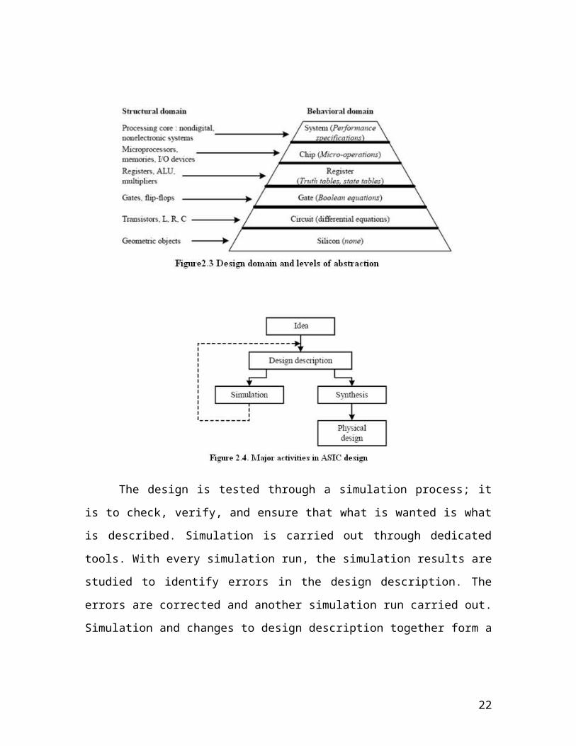
2.3.1. Abstraction model
The model divides the whole design cycle into various domains. With such an
abstraction through a division process the design is carried out in different layers. The
designer at one layer can function without bothering about the layers above or below. The
thick horizontal lines separating the layers in the figure signify the compartmentalization.
As an example, let us consider design at the gate level. The circuit to be designed would
be described in terms of truth tables and state tables. With these as available inputs, he
has to express them as Boolean logic equations and realize them in terms of gates and
flip-flops. In turn, these form the inputs to the layer immediately below.
Compartmentalization of the approach to design in the manner described here is the
essence of abstraction; it is the basis for development and use of CAD tools in VLSI
design at various levels.
The design methods at different levels use the respective aids such as Boolean
equations, truth tables, state transition table, etc. But the aids play only a small role in the
process. To complete a design, one may have to switch from one tool to another, raising
the issues of tool compatibility and learning new environments.
13

2.4. ASIC DESIGN FLOW
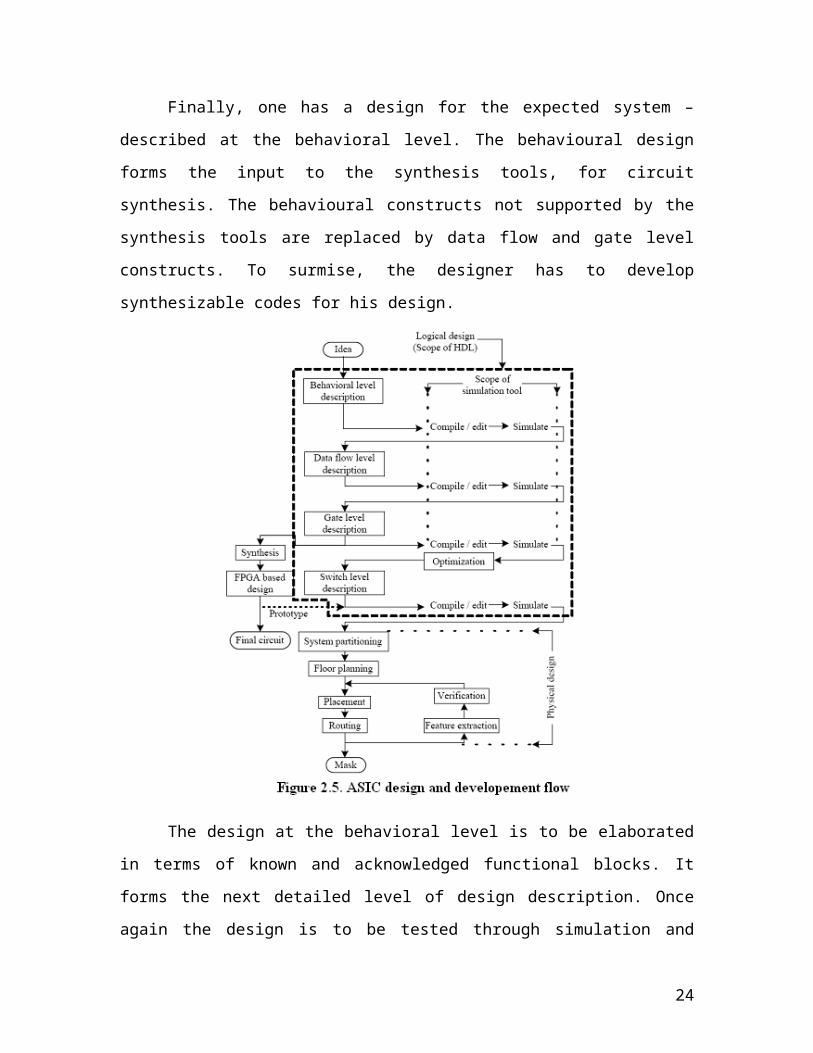
As with any other technical activity, development of an ASIC starts with an idea
and takes tangible shape through the stages of development as shown in Figure 1.4 and
shown in detail in Figure 1.5. The first step in the process is to expand the idea in terms
of behavior of the target circuit. Through stages of programming, the same is fully
developed into a design description – in terms of well defined standard constructs and
conventions.
The design is tested through a simulation process; it is to check, verify, and ensure
that what is wanted is what is described. Simulation is carried out through dedicated
14
tools. With every simulation run, the simulation results are studied to identify errors in
the design description. The errors are corrected and another simulation run carried out.
Simulation and changes to design description together form a cyclic iterative process,
repeated until an error-free design is evolved.
Design description is an activity independent of the target technology or
manufacturer. It results in a description of the digital circuit. To translate it into a tangible
circuit, one goes through the physical design process. The same constitutes a set of
activities closely linked to the manufacturer and the target
Technology
2.4.1. Design Description
The design is carried out in stages. The process of transforming the idea into a
detailed circuit description in terms of the elementary circuit components constitutes
design description. The final circuit of such an IC can have up to a billion such
components; it is arrived at in a step-by-step manner.
The first step in evolving the design description is to describe the circuit in terms
of its behavior. The description looks like a program in a high level language like C.
Once the behavioral level design description is ready, it is tested extensively with the
help of a simulation tool; it checks and confirms that all the expected functions are
carried out satisfactorily. If necessary, this behavioral level routine is edited, modified,
and rerun – all done manually.
Finally, one has a design for the expected system – described at the behavioral
level. The behavioural design forms the input to the synthesis tools, for circuit synthesis.
The behavioural constructs not supported by the synthesis tools are replaced by data flow
and gate level constructs. To surmise, the designer has to develop synthesizable codes for
his design.
15

The design at the behavioral level is to be elaborated in terms of known and
acknowledged functional blocks. It forms the next detailed level of design description.
Once again the design is to be tested through simulation and iteratively corrected for
errors. The elaboration can be continued one or two steps further. It leads to a detailed
design description in terms of logic gates and transistor switches.
2.4.2. Optimization
The circuit at the gate level – in terms of the gates and flip-flops – can be
redundant in nature. The same can be minimized with the help of minimization tools. The
step is not shown separately in the figure. The minimized logical design is converted to a
circuit in terms of the switch level cells from standard libraries provided by the foundries.
The cell based design generated by the tool is the last step in the logical design process; it
forms the input to the first level of physical design [Micheli].
16

2.4.3. Simulation
The design descriptions are tested for their functionality at every level –
behavioral, data flow, and gate. One has to check here whether all the functions are
carried out as expected and rectify them. All such activities are carried out by the
simulation tool. The tool also has an editor to carry out any corrections to the source
code. Simulation involves testing the design for all its functions, functional sequences,
timing constraints, and specifications. Normally testing and simulation at all the levels –
behavioral to switch level – are carried out by a single tool; the same is identified as
“scope of simulation tool” in Figure 1.5.
2.4.4. Synthesis
With the availability of design at the gate (switch) level, the logical design is
complete. The corresponding circuit hardware realization is carried out by a synthesis
tool. Two common approaches are as follows:
The circuit is realized through an FPGA [Oldfield]. The gate level design description is
the starting point for the synthesis here. The FPGA vendors provide an interface to the
synthesis tool. Through the interface the gate level design is realized as a final circuit.
With many synthesis tools, one can directly use the design description at the data flow
level itself to realize the final circuit through an FPGA. The FPGA route is attractive for
limited volume production or a fast development cycle.
The circuit is realized as an ASIC. A typical ASIC vendor will have his own
library of basic components like elementary gates and flip-flops. Eventually the circuit is
to be realized by selecting such components and interconnecting them conforming to the
required design. This constitutes the physical design. Being an elaborate and costly
process, a physical design may call for an intermediate functional verification through the
FPGA route. The circuit realized through the FPGA is tested as a prototype. It provides
another opportunity for testing the design closer to the final circuit.
2.4.5. Physical Design
A fully tested and error-free design at the switch level can be the starting point for
a physical design [Baker & Boyce, Wolf]. It is to be realized as the final circuit using
17

(typically) a million components in the foundry’s library. The step-by-step activities in
the process are described briefly as follows:
• System partitioning : The design is partitioned into convenient compartments or
functional blocks. Often it would have been done at an earlier stage itself and the
software design prepared in terms of such blocks. Interconnection of the blocks is part of
the partition process.
• Floor planning : The positions of the partitioned blocks are planned and the blocks are
arranged accordingly. The procedure is analogous to the planning and arrangement of
domestic furniture in a residence. Blocks with I/O pins are kept close to the periphery;
those which interact frequently or through a large number of interconnections are kept
close together, and so on. Partitioning and floor planning may have to be carried out and
refined iteratively to yield best results.
• Placement: The selected components from the ASIC library are placed in position on
the “Silicon floor.” It is done with each of the blocks above.
• Routing: The components placed as described above are to be interconnected to the rest
of the block: It is done with each of the blocks by suitably routing the interconnects.
Once the routing is complete, the physical design cam is taken as complete. The final
mask for the design can be made at this stage and the ASIC manufactured in the foundry.
2.4.6. Post Layout Simulation
Once the placement and routing are completed, the performance specifications
like silicon area, power consumed, path delays, etc., can be computed. Equivalent circuit
can be extracted at the component level and performance analysis carried out. This
constitutes the final stage called “verification.” One may have to go through the
placement and routing activity once again to improve performance.
2.4.7. Critical Subsystems
The design may have critical subsystems. Their performance may be crucial to the
overall performance; in other words, to improve the system performance substantially,
one may have to design such subsystems afresh. The design here may imply redefinition
of the basic feature size of the component, component design, placement of components,
18
or routing done separately and specifically for the subsystem. A set of masks used in the
foundry may have to be done afresh for the purpose.
2.5. ROLE OF HDL
An HDL provides the framework for the complete logical design of the ASIC. All
the activities coming under the purview of an HDL are shown enclosed in bold dotted
lines in Figure 1.4. Verilog and VHDL are the two most commonly used HDLs today.
Both have constructs with which the design can be fully described at all the levels. There
are additional constructs available to facilitate setting up of the test bench, spelling out
test vectors for them and “observing” the outputs from the designed unit.
IEEE has brought out Standards for the HDLs, and the software tools conform to
them. Verilog as an HDL was introduced by Cadence Design Systems; they placed it into
the public domain in 1990. It was established as a formal IEEE Standard in 1995. The
revised version has been brought out in 2001. However, most of the simulation tools
available today conform only to the 1995 version of the standard.VHDL used by a
substantial number of the VLSI designers today is the used in this project for modelling
the design.
19

CHAPTER 3
FIELD PROGRAMMABLE GATE ARRAY (FPGA)
A field-programmable gate array (FPGA) is a semiconductor device that can be
configured by the customer or designer after manufacturing—hence the name "field-
programmable". FPGAs are programmed using a logic circuit diagram or a source code
in a hardware description language (HDL) to specify how the chip will work. They can
be used to implement any logical function that an application-specific integrated circuit
(ASIC) could perform, but the ability to update the functionality after shipping offers
advantages for many applications.
FPGAs contain programmable logic components called "logic blocks", and a
hierarchy of reconfigurable interconnects that allow the blocks to be "wired together".
Fully fabricated FPGA chips containing thousands of logic gates or even more, with
programmable interconnects, are available to users for their custom hardware
programming to realize desired functionality. This design style provides a means for fast
prototyping and also for cost-effective chip design, especially for low-volume
applications. A typical field programmable gate array (FPGA) chip consists of I/O
buffers, an array of configurable logic blocks (CLBs), and programmable interconnect
structures. The programming of the interconnects is implemented by programming of
RAM cells whose output terminals are connected to the gates of MOS pass transistors.
The typical design flow of an FPGA chip starts with the behavioral description of its
functionality, using a hardware description language such as VHDL.
3.1 FIELD PROGRAMMABLE
Field Programmable means that the FPGA's function is defined by a user's
program rather than by the manufacturer of the device. A typical integrated circuit
performs a particular function defined at the time of manufacture. In contrast, the
FPGA's function is defined by a program written by someone other than the device
manufacturer. Depending on the particular device, the program is either ‘burned’
in permanently or semi-permanently as part of a board assembly process, or is loaded
20
from an external memory each time the device is powered up. This user programmability
gives the user access to complex integrated designs without the high engineering costs
associated with application specific integrated circuits.
3.2 LOGIC CELL
The logic cell architecture varies between different device families. Generally
speaking, each logic cell combines a few binary inputs (typically between 3 and 10) to
one or two outputs according to a boolean logic function specified in the user program
In most families, the user also has the option of registering the combinatorial
output of the cell, so that clocked logic can be easily implemented. The cell's
combinatorial logic may be physically implemented as a small look-up table memory
(LUT) or as a set of multiplexers and gates. LUT devices tend to be a bit more flexible
and provide more inputs per cell than multiplexer cells at the expense of propagation
delay.
3.3 ARCHITECTURE
The most common FPGA architecture consists of an array of configurable logic
blocks (CLBs), I/O pads, and routing channels. Generally, all the routing channels have
the same width (number of wires). Multiple I/O pads may fit into the height of one row or
the width of one column in the array.
21
An application circuit must be mapped into an FPGA with adequate resources.
While the number of CLBs and I/Os required are easily determined from the design, the
amount of routing tracks needed may vary considerably even among designs with the
same amount of logic. (For example, a crossbar switch requires much more routing than a
systolic array with the same gate count.) Since unused routing tracks increase the cost
(and decrease the performance) of the part without providing any benefit, FPGA
manufacturers try to provide just enough tracks so that most designs that will fit in terms
of LUTs and IOs can be routed.
A classic FPGA logic block consists of a 4-input lookup table (LUT), and a flip-
flop, as shown below. In recent years, manufacturers have started moving to 6-input
LUTs in their high performance parts, claiming increased performance. There is only one
output, which can be either the registered or the unregistered LUT output. The logic
block has four inputs for the LUT and a clock input. Since clock signals (and often other
high-fanout signals) are normally routed via special-purpose dedicated routing networks
in commercial FPGAs, they and other signals are separately managed.
Each input is accessible from one side of the logic block, while the output pin can
connect to routing wires in both the channel to the right and the channel below the logic
block. Each logic block output pin can connect to any of the wiring segments in the
channels adjacent to it. Similarly, an I/O pad can connect to any one of the wiring
segments in the channel adjacent to it. For example, an I/O pad at the top of the chip can
connect to any of the W wires (where W is the channel width) in the horizontal channel
immediately below it.
Generally, the FPGA routing is unsegmented. That is, each wiring segment spans
only one logic block before it terminates in a switch box. By turning on some of the
programmable switches within a switch box, longer paths can be constructed. For higher
speed interconnect, some FPGA architectures use longer routing lines that span multiple
logic blocks.
22

Whenever a vertical and a horizontal channel intersect, there is a switch box. In
this architecture, when a wire enters a switch box, there are three programmable switches
that allow it to connect to three other wires in adjacent channel segments. The pattern, or
topology, of switches used in this architecture is the planar or domain-based switch box
topology. In this switch box topology, a wire in track number one connects only to wires
in track number one in adjacent channel segments, wires in track number 2 connect only
to other wires in track number 2 and so on.
Modern FPGA families expand upon the above capabilities to include higher level
functionality fixed into the silicon. Having these common functions embedded into the
silicon reduces the area required and gives those functions increased speed compared to
building them from primitives. FPGAs are also widely used for systems validation
including pre-silicon validation, post-silicon validation, and firmware development. This
allows chip companies to validate their design before the chip is produced in the factory,
reducing the time to market.
3.4 FPGA PROGRAMS
Individually defining the many switch connections and cell logic functions would
be a daunting task. Fortunately, this task is handled by special software. The software
translates a user's schematic diagrams or textual hardware description language code then
places and routes the translated design. Most of the software packages have hooks to
allow the user to influence implementation, placement and routing to obtain better
performance and utilization of the device. Libraries of more complex function macros
(eg. adders) further simplify the design process by providing common circuits that are
already optimized for speed or area.
3.5 FPGA PROGRAMMING
To define the behavior of the FPGA, the user provides a hardware description
language (HDL) or a schematic design. The HDL form might be easier to work with
when handling large structures because it's possible to just specify them numerically
23
rather than having to draw every piece by hand. On the other hand, schematic entry can
allow for easier visualization of a design.
Then, using an electronic design automation tool, a technology-mapped netlist is
generated. The netlist can then be fitted to the actual FPGA architecture using a process
called place-and-route, usually performed by the FPGA company's proprietary place-and-
route software. The user will validate the map, place and route results via timing analysis,
simulation, and other verification methodologies. Once the design and validation process
is complete, the binary file generated (also using the FPGA company's proprietary
software) is used to (re)configure the FPGA.
Going from schematic/HDL source files to actual configuration: The source files
are fed to a software suite from the FPGA/CPLD vendor that through different steps will
produce a file. This file is then transferred to the FPGA/CPLD via a serial interface
(JTAG) or to an external memory device like an EEPROM.
The most common HDLs are VHDL and Verilog, although in an attempt to
reduce the complexity of designing in HDLs, which have been compared to the
equivalent of assembly languages, there are moves to raise the abstraction level through
the introduction of alternative languages.
To simplify the design of complex systems in FPGAs, there exist libraries of
predefined complex functions and circuits that have been tested and optimized to speed
up the design process. These predefined circuits are commonly called IP cores, and are
available from FPGA vendors and third-party IP suppliers. Other predefined circuits are
available from developer communities such as OpenCores (typically free, and released
under the GPL, BSD or similar license), and other sources.
In a typical design flow, an FPGA application developer will simulate the design
at multiple stages throughout the design process. Initially the RTL description in VHDL
or Verilog is simulated by creating test benches to simulate the system and observe
results. Then, after the synthesis engine has mapped the design to a netlist, the netlist is
translated to a gate level description where simulation is repeated to confirm the synthesis
24

proceeded without errors. Finally the design is laid out in the FPGA at which point
propagation delays can be added and the simulation run again with these values back-
annotated onto the netlist.
3.6 APPLICATIONS
Applications of FPGAs include digital signal processing, software-defined radio,
aerospace and defense systems, ASIC prototyping, medical imaging, computer vision,
speech recognition, cryptography, bioinformatics, computer hardware emulation and a
growing range of other areas.
FPGAs especially find applications in any area or algorithm that can make use of
the massive parallelism offered by their architecture. One such area is code breaking, in
particular brute-force attack, of cryptographic algorithms. FPGAs are increasingly used in
conventional high performance computing applications where computational kernels such
as FFT or Convolution are performed on the FPGA instead of a microprocessor.
The largest advantage of FPGA-based design is the very short turn-around time,
i.e., the time required from the start of the design process until a functional chip is
available. Since no physical manufacturing step is necessary for customizing the FPGA
chip, a functional sample can be obtained almost as soon as the design is mapped into a
specific technology. The typical price of FPGA chips are usually higher than other
realization alternatives (such as gate array or standard cells) of the same design, but for
small-volume production of ASIC chips and for fast prototyping, FPGA offers a very
valuable option.
25

CHAPTER 4
HARDWARE DESCRIPTION LANGUAGE
In electronics, a hardware description language or HDL is any language from a
class of computer languages and/or programming languages for formal description of
digital logic and electronic circuits. It can describe the circuit's operation, its design and
organization, and tests to verify its operation by means of simulation.
HDLs are standard text-based expressions of the spatial and temporal structure
and behaviour of electronic systems. In contrast to a software programming language,
HDL syntax and semantics include explicit notations for expressing time and
concurrency, which are the primary attributes of hardware. Languages whose only
characteristic is to express circuit connectivity between a hierarchy of blocks are properly
classified as netlist languages used on electric computer-aided design (CAD).
HDLs are used to write executable specifications of some piece of hardware. A
simulation program, designed to implement the underlying semantics of the language
statements, coupled with simulating the progress of time, provides the hardware designer
with the ability to model a piece of hardware before it is created physically. It is this
executability that gives HDLs the illusion of being programming languages. Simulators
capable of supporting discrete-event (digital) and continuous-time (analog) modeling
exist, and HDLs targeted for each are available.
It is certainly possible to represent hardware semantics using traditional
programming languages such as C++, although to function such programs must be
augmented with extensive and unwieldy class libraries. Primarily, however, software
programming languages do not include any capability for explicitly expressing time, and
this is why they do not function as a hardware description language. Before the recent
introduction of SystemVerilog, C++ integration with a logic simulator was one of the few
ways to use OOP in hardware verification. SystemVerilog is the first major HDL to offer
object orientation and garbage collection.
26

Using the proper subset of virtually any (hardware description or software
programming) language, a software program called a synthesizer (or synthesis tool) can
infer hardware logic operations from the language statements and produce an equivalent
netlist of generic hardware primitives to implement the specified behaviour. Synthesizers
generally ignore the expression of any timing constructs in the text. Digital logic
synthesizers, for example, generally use clock edges as the way to time the circuit,
ignoring any timing constructs. The ability to have a synthesizable subset of the language
does not itself make a hardware description language.
For a given algorithm, leveraging the parallelism of custom hardware will
generally outperform software at the cost of a greater development budget. Designing a
system in HDL is generally much harder and more time consuming than writing a
software program to do the same thing. Consequently, there has been much work done on
automatic conversion of C code into HDL, but this has not reached a high level of
commercial success.
4.1 HDL AND PROGRAMMING LANGUAGES
A HDL is analogous to a software programming language, but with major
differences. Programming languages are inherently procedural (single-threaded), with
limited syntactical and semantic support to handle concurrency. HDLs, on the other hand,
can model multiple parallel processes (such as flipflops, adders, etc.) that automatically
execute independently of one another. Any change to the process's input automatically
triggers an update in the simulator's process stack. Both programming languages and
HDLs are processed by a compiler (usually called a synthesizer in the HDL case), but
with different goals. For HDLs, 'compiler' refers to synthesis, a process of transforming
the HDL code listing into a physically realizable gate netlist. The netlist output can take
any of many forms: a "simulation" netlist with gate-delay information, a "handoff" netlist
for post-synthesis place and route, or a generic industry-standard EDIF format (for
subsequent conversion to a JEDEC-format file).
27
On the other hand, a software compiler converts the source-code listing into a
microprocessor-specific object-code, for execution on the target microprocessor. As
HDLs and programming languages borrow concepts and features from each other, the
boundary between them is becoming less distinct. However, pure HDLs are unsuitable
for general purpose software application development, just as general-purpose
programming languages are undesirable for modeling hardware. Yet as electronic
systems grow increasingly complex, and reconfigurable systems become increasingly
mainstream, there is growing desire in the industry for a single language that can perform
some tasks of both hardware design and software programming. SystemC is an example
of such—embedded system hardware can be modeled as non-detailed architectural blocks
(blackboxes with modeled signal inputs and output drivers). The target application is
written in C/C++, and natively compiled for the host-development system (as opposed to
targeting the embedded CPU, which requires host-simulation of the embedded CPU). The
high level of abstraction of SystemC models is well suited to early architecture
exploration, as architectural modifications can be easily evaluated with little concern for
signal-level implementation issues.
In an attempt to reduce the complexity of designing in HDLs, which have been
compared to the equivalent of assembly languages, there are moves to raise the
abstraction level of the design. Companies such as Cadence, Synopsys and Agility
Design Solutions are promoting SystemC as a way to combine high level languages with
concurrency models to allow faster design cycles for FPGAs than is possible using
traditional HDLs. Approaches based on standard C or C++ (with libraries or other
extensions allowing parallel programming) are found in the Catapult C tools from Mentor
Graphics, and in the Impulse C tools from Impulse Accelerated Technologies. Annapolis
Micro Systems, Inc.'s CoreFire Design Suite and National Instruments LabVIEW FPGA
provide a graphical dataflow approach to high-level design entry. Languages such as
SystemVerilog, SystemVHDL, and Handel-C seek to accomplish the same goal, but are
aimed at making existing hardware engineers more productive versus making FPGAs
more accessible to existing software engineers. Thus SystemVerilog is more quickly and
28

widely adopted than SystemC. There is more information on C to HDL and Flow to HDL
in their respective articles.
4.2 LANGUAGES
The two most widely-used and well-supported HDL varieties used in industry are:
VHDL
Verilog
Others include :
Advanced Boolean Expression Language (ABEL)
AHDL (Altera HDL, a proprietary language from Altera)
Atom (behavioral synthesis and high-level HDL based on Haskell)
Bluespec (high-level HDL originally based on Haskell, now with a SystemVerilog
syntax)
Confluence (a functional HDL; has been discontinued)
CUPL (a proprietary language from Logical Devices, Inc.)
Handel-C (a C-like design language)
C-to-Verilog (Converts C to Verilog)
HDCaml (based on Objective Caml)
Hardware Join Java (based on Join Java)
HML (based on SML)
Hydra (based on Haskell)
Impulse C (another C-like language)
JHDL (based on Java)
Lava (based on Haskell)
Lola (a simple language used for teaching)
MyHDL (based on Python)
PALASM (for Programmable Array Logic (PAL) devices)
Ruby (hardware description language)
RHDL (based on the Ruby programming language)
29
4.2.1 Verilog
In the semiconductor and electronic design industry, Verilog is a hardware
description language (HDL) used to model electronic systems. Verilog HDL, not to be
confused with VHDL, is most commonly used in the design, verification, and
implementation of digital logic chips at the Register transfer level (RTL) level of
abstraction. It is also used in the verification of analog and mixed-signal circuits. Verilog
was invented by Phil Moorby and Prabhu Goel during the winter of 1983/1984 at
Automated Integrated Design Systems (later renamed to Gateway Design Automation in
1985) as a hardware modeling language. Gateway Design Automation was later
purchased by Cadence Design Systems in 1990. Cadence now has full proprietary rights
to Gateway's Verilog and the Verilog-XL simulator logic simulators.
4.2.2 Verilog 95
With the increasing success of VHDL at the time, Cadence decided to make the
language available for open standardization. Cadence transferred Verilog into the public
domain under the Open Verilog International (OVI) (now known as Accellera)
organization. Verilog was later submitted to IEEE and became IEEE Standard 1364-
1995, commonly referred to as Verilog-95.
In the same time frame Cadence initiated the creation of Verilog-A to put
standards support behind its analog simulator Spectre. Verilog-A was never intended to
be a standalone language and is a subset of Verilog-AMS which encompassed Verilog-
95.
4.2.3 Verilog 2001
Extensions to Verilog-95 were submitted back to IEEE to cover the deficiencies
that users had found in the original Verilog standard. These extensions became IEEE
Standard 1364-2001 known as Verilog-2001.
Verilog-2001 is a significant upgrade from Verilog-95. First, it adds explicit
support for (2's complement) signed nets and variables. Previously, code authors had to
30

perform signed-operations using awkward bit-level manipulations. The same function
under Verilog-2001 can be more succinctly described by one of the built-in operators: +,
-, /, *, >>>. A generate/endgenerate construct (similar to VHDL's generate/endgenerate)
allows Verilog-2001 to control instance and statement instantiation through normal
decision-operators (case/if/else).
Using generate/end generate, Verilog-2001 can instantiate an array of instances,
with control over the connectivity of the individual instances. File I/O has been improved
by several new system-tasks. And finally, a few syntax additions were introduced to
improve code-readability (eg. always @*, named-parameter override, C-style
function/task/module header declaration.)
Verilog-2001 is the dominant flavor of Verilog supported by the majority of
commercial EDA software packages.
4.2.4 Verilog 2005
Not to be confused with SystemVerilog, Verilog 2005 (IEEE Standard 1364-
2005) consists of minor corrections, spec clarifications, and a few new language features
(such as the uwire keyword). A separate part of the Verilog standard , Verilog-AMS,
attempts to integrate analog and mixed signal modelling with traditional Verilog.
4.2.5 System Verilog
SystemVerilog is a superset of Verilog-2005, with many new features and
capabilities to aid design-verification and design-modeling. The advent of High Level
Verification languages such as OpenVera, and Verisity's E language encouraged the
development of Superlog by Co-Design Automation Inc. Co-Design Automation Inc was
later purchased by Synopsys. The foundations of Superlog and Vera were donated to
Accellera, which later became the IEEE standard P1800-2005: SystemVerilog.
31

CHAPTER 5
SINGLE CHANNEL UART
A universal asynchronous receiver/transmitter is a type of "asynchronous
receiver/transmitter", a piece of computer hardware that translates data between parallel
and serial forms. UARTs are commonly used in conjunction with other communication
standards such as EIA RS-232.
5.1 NEED OF UART
Control the receiving and transmitting time of the data.
The UART receiver is responsible for the synchronization of the serial data
stream and the recovery of data characters.
Increase the accuracy and decrease the effect of the noise:
The UART system can tolerate a moderate amount of system noise without losing
any information.
5.2. UART DATA FORMAT
UART data format comprises of 11 bits.
Active low start bit, Data bits (8), Parity bit, High stop bit
Figure 5.1 UART data format
32

The transmit and receive line of the UART are held high while no
transmission/reception is taking place. In the transmission of a sequence the active low
start bit indicates to the receiving UART that a new sequence of data is on its way. This
causes the receiving UART to take the next 8 bits as the transmitted data and the bit after
that as the parity of these 8 data-bits. Lastly, a high stop bit is used to indicate the end of
a block. The parity can be set as even or odd and is used to indicate whether or not there
has been an error in the received data bits. Note that errors can still occur even if the
parity bit indicates no parity errors. For example, if the transmitted sequence is
"11110000" and the parity is set as even, the parity bit that would be transmitted with the
sequence would be '0'. If the received sequence is "11101000", the calculated parity of
this sequence also equals the transmitted parity bit of '0', thereby fooling the receiving
UART into thinking that there were no errors in transmission.
5.3. SINGLE CHANNEL UART BLOCK DIAGRAM
Figure 5.2 Single channel UART block diagram
33

The UART takes bytes of data and transmits the individual bits in a sequential fashion
and also it takes the data in serial form and converts it into
Bytes and sends to CPU.
5.4. TRANSMITTER STATE MACHINE
When a word is given to the UART for Asynchronous transmissions, a bit called
the "Start Bit" is added to the beginning of each word that is to be transmitted. The Start
Bit is used to alert the receiver that a word of data is about to be sent, and to force the
clock in the receiver into synchronization with the clock in the transmitter.
After the Start Bit, the individual bits of the word of data are sent, with the Least
Significant Bit (LSB) being sent first. When the entire data word has been sent, the
transmitter may add a Parity Bit that the transmitter generates. The Parity Bit may be
used by the receiver to perform simple error checking. Then at least one Stop Bit is sent
by the transmitter.
Block Diagram
Figure 5.3 Transmitter state machine
Different inputs and outputs for the Transmitter is shown in figure. Tx_en works
as enable to this block. Whenever it is high then only it transmits the data if it is low then
the transmitter state machine stays in IDLE state. Din is input to this block which is 8
bit.Parity_en works as enable to parity state i.e. if it is high then only it will go to parity
34

state. Parity_in depends on the number of ones in the input Din which is generated by the
Parity Generator.
Sout is output of the Transmitter Block which is in serial form. Tx_Rinc is Read
enable to Transmitter FIFO. If data Transferring is going on then Data active will be high
which one of the outputs of Transmitter State Machine is.
5.5. PARITY GENERATOR
Parity Generator generates parity bit to the transmit data. The Parity Bit may be
used by the receiver to perform simple error checking. The inputs to the Parity Generator
are Din_Tx and odd_even_ parity. Din_tx is transmitted data and odd_even_parity is
used to generate parity TX by XORing with Din_Tx.
Example: Assume the at Din is 4 bit
Parity_Tx = odd_even_parity ^ Din_Tx (3) ^ Din_Tx (2) ^ Din_Tx (1) ^ Din_Tx (0);
Block Diagram
Figure 5.4 Parity generator
5.6. RECEIVER STATE MACHINE
When the receiver has received all of the bits in the data word, it may check for
the Parity Bits (both sender and receiver must agree on whether a Parity Bit is to be
35
used), and then the receiver looks for a Stop Bit. If the Stop Bit does not appear when it is
supposed to, the UART considers the entire word to be garbled and will report a Framing
Error to the host processor when the data word is read. The usual cause of a Framing
Error is that the sender and receiver clocks were not running at the same speed, or that the
signal was interrupted.
Regardless of whether the data was received correctly or not, the UART
automatically discards the Start, Parity and Stop bits. If the sender and receiver are
configured identically, these bits are not passed to the host.
If another word is ready for transmission, the Start Bit for the new word can be
sent as soon as the Stop Bit for the previous word has been sent.
Block Diagram
Figure 5.5 Receiver state machine
5.7. TRANSMITTER FIFO
FIFOs are often used to safely pass data from one clock domain to
another asynchronous clock domain. Here we are using single clock for both Reading and
36

Writing the Data. Data_in is input to the FIFO which is 8 bit. . If winc is high then only
FIFO accepts the Data and Rinc is high then only we can read the data from the FIFO.
Full and Empty are the outputs of the FIFO. If FIFO is full then full will be high and if it
is empty then empty becomes high.
Block Diagram:
Figure 5.6 Transmitter FIFO
37

CHAPTER 6
MULTI-CHANNEL UART
6.1. MULTI-CHANNEL UART
Figure 6.1 MULTI CHANNEL UART
This contains nine blocks. Those are four Uarts, two asynchronous FIFOs,
Controller block, Register block and Baud rate Generator. Each and every individual
block explanation is given below.
6.2. BAUD RATE GENERATOR
The Baud Rate simply “The rate of data Transmission expressed in bits per second,
Kilo bits per second or Mega bits per second. The Baud Rate Generator generates
different Baud rates for different Uarts.Clk1, CLk2, Clk3 and Clk4 are the different
clocks which are generated by this Baud rate generator depends on the input
38

clk_div_values. Clk1_en, Clk2_en, Clk3_en and Clk4_en are enables to generate Clk1,
Clk2, Clk3 and Clk4.
Block Diagram
Figure 6.2 Baud rate generator
6.3. ASYNCHRONOUS FIFO
FIFOs are often used to safely pass data from one clock domain to another
asynchronous clock domain. An asynchronous FIFO refers to a FIFO design where data
values are written to a FIFO buffer from one clock
Domain and the data values are read from the same FIFO buffer from another
clock domain. This is 64x8 FIFO. In this Wclk is used to write the data into the FIFO and
Rclk is used to read the Data from the FIFO. If winc is high then only FIFO accepts the
Data and Rinc is high then only we can read the data from the FIFO. Full and Empty are
the outputs of the FIFO. If FIFO is full then full will be high and if it is empty then empty
becomes high.
Block Diagram
39

Figure 6.3 Asynchronous FIFO
6.4. ASYNCHRONOUS FIFO BLOCK DIAGRAM
Figure 6.4 Asynchronous FIFO block diagram
FIFOMem: This is the FIFO memory that is accessed by the both the write and read
clock domains. This buffer is most likely an instantiated, synchronous dual port RAM.
Other memory styles can be adapted to function as a FIFO buffer.
40

Sync_r2w: This is the synchronizer block used to synchronize the read pointer into the
write clock domain. The synchronized read pointer will be used by the Wptr_full block to
generate the write full condition. This block only contains flip flops that are synchronized
to the write clock domain. No other logic is included in that.
Sync_w2r: This is the synchronizer block that is used to synchronize the write pointer
into the read clock domain. The synchronized write pointer will be used by the
Rptr_Empty block to generate the FIFO Empty condition. This block only contains flip
flops that are synchronized to the read clock domain. No other
Logic is included in that.
Wptr_full: This block is completely synchronous to the write clock domain and contains
FIFO write pointer and full flag logic.
Rptr_Empty: This block is completely synchronous to the read clock domain and
contains the FIFO read pointer and Empty flag logic.
In order to perform FIFO Full and Empty tests using this FIFO style the read
and write pointers must be passed to opposite clock domain for pointer comparison
6.5. CONTROLLER
Clock Controller controls the multi channel uart. If cs is high then it goes from
IDLE state to Program State. In program state all clock enables are assigned to zero and
when mode_sel(0) is high then it will go to Run state. In run state all clock enables
(Clk1_en, Clk2_en, Clk3_en, and Clk4_en) will become ‘1’. In Run state if mode_sel (2
down to 1) is “00” then Normal mode will become high , if it is”01” then hub_mode will
high, if it is “11” then bridge mode will become high.
Block Diagram
41

Figure 6.5 Controller
Internal Structure:
Figure 6.6 Internal structure of controller
6.6. REGISTER BLOCK
Reg block is one which contains different registers. Total 12 registers are there
in the Reg block. They are Mode register, Status register, configuration registers, clock
division registers, transmitter registers, and receiver registers e.t.c. If wr_rd is high then
42

depends on address it write the data to different registers, if it is low then it reads data
from different registers and data will send to reg_data_out.All registers are not writable.
Example status register and receive registers are not writable.
Block Diagram:
Figure 6.7 Block diagram of Register block
ALGORITHM
1. Start.
2. Initialize.
3. Check for the mode.
4. Depending on type of mode it will start working.
5. Master and slave equipments are set at different baud rates.
6. The controller can be reconfigurable using different registers.
7. We implemented UART using FIFO’s to reduce the synchronization error
between subsystems in a system with several subsystems.
8. FIFO checks for the read/write condition, if it is write it checks for FIFO full, if is
not full it will start writing. If it is read it checks for FIFO empty if it is not empty it
will start reading.
9. Depending on the enable values it will either transmit or receive.
10. Stop.
43

SCOPE OF FUTURE DEVELOPMENT
The increasing growth of sub-micron technology has resulted in the difficulty of
testing. Design and test engineers have no choice but to accept new responsibilities that
had been performed by groups of technicians in the previous years. Design engineers who
do not design systems with full testability in mind open themselves to the increased
possibility of product failures and missed market opportunities. BIST is a design
technique that allows a circuit to test itself. One of the most popular test techniques is
called Built-In-Self-Test (BIST).
A BIST Universal Asynchronous Receive/Transmit (UART) has the objectives of
firstly to satisfy specified testability requirements, and secondly to generate the lowest-
cost with the highest performance implementation. UART has been an important
input/output tool for decades and is still widely used. Although BIST techniques are
becoming more common in industry, the additional BIST circuit that increases the
hardware overhead increases design time and performance degradation is often cited as
the reason for the limited use of BIST.
44

The technique can provide shorter test time compared to an externally applied test
and allows the use of low-cost test equipment during all stages of production.
In the implementation phase, the BIST technique will be incorporated into the
UART design before the overall design is synthesized by means of reconfiguring the
existing design to match testability requirements. The UART is targeted at broadband
modem, base station, cell phone, and PDA designs.
CONCLUSION
This introduces a design method of Asynchronous FIFO. Using this FIFO it
implements a Multi Channel Uart with in a FPGA based on SRAM with high speed and
high Reliability. The Controller can be used to implement communications in complex
system with different Baud Rates of sub controllers and also it can be used to reduce the
delays between sub controllers of a complex control system to improve the
synchronization of each sub controller. The Controller is Reconfigurable and Scalable
45
BIBLIOGRAPHY
[1] S. E. Lyshevski, “Control Systems Theory with Engineering Applications”,
Birkhauser Boston, 2001
[2] L. K. Hu and Q.CH. Wang, “UART-based Reliable Communication and performance
Analysis” , Computer Engineering, Vol 32 No. 10, May 2006, pp15-21
[3] F.S. Pan, F. ZHAO, J. Xi and Y. Luo, “Implement of Parallel Signal Processing
Syttem Based on FPGA and Multi-DSP”, Computer Engineering Vol 32, No. 23, Dec
2006, pp247-249
[4] X. D. Wu and B. Dai, “Design of Interface Between High Speed A/D and DSP Based
on FIFO”, Journal of Beijing Institute of Petrochemica Technology Vol 14 No.12, June
2006, pp26-29
[5] C. E. Cummings, “Simulation and Synthesis Techniques for Asynchronous FIFO
Design”, SNUG San Jose 2002
[6] C. E. Cummings, “Simulation and Synthesis Techniques for Asynchronous FIFO
Design with Asynchronous Pointer Comparisons”, SNUG San Jose 2002
[7] Vijay A. Nebhrajan, “Asynchronous FIFO Architectures”, www.eebyte.com
46

[8] X., Yang, “Industrial Data Communication and Control Networks”, Beijing: TUP,
2003.6
[9] B. Zeidman, “Designing with FPGAs & CPLDs”, CMP Books, 2002
47